Embed Size (px)
Citation preview

FEATURES
� Single Power Supply Operation- Low voltage range: 2.7 V - 3.6 V
• Memory Organization- Pm39LV512: 64K x 8 (512 Kbit)- Pm39LV010: 128K x 8 (1 Mbit)- Pm39LV020: 256K x 8 (2 Mbit)- Pm39LV040: 512K x 8 (4 Mbit)
• High Performance Read- 55/70 ns access time
• Cost Effective Sector/Block Architecture- Uniform 4 Kbyte sectors- Uniform 64 Kbyte blocks (sector group - exceptPm39LV512)
• Data# Polling and Toggle Bit Features
• Hardware Data Protection
• Automatic Erase and Byte Program- Build-in automatic program verification- Typical 16 µs/byte programming time- Typical 55 ms sector/block/chip erase time
• Low Power Consumption- Typical 4 mA active read current- Typical 8 mA program/erase current- Typical 0.1 µA CMOS standby current
• High Product Endurance- Guarantee 100,000 program/erase cycles per
single sector (preliminary)- Minimum 20 years data retention
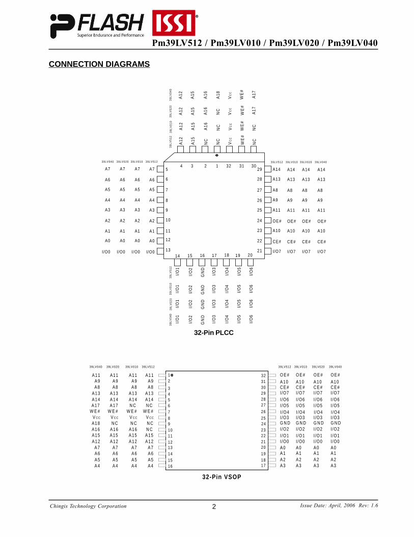
• Industrial Standard Pin-out and Packaging- 32-pin (8 mm x 14 mm) VSOP- 32-pin PLCC- Optional lead-free (Pb-free) package
GENERAL DESCRIPTION
The Pm39LV512/010/020/040 are 512 Kbit/1 Mbit/2 Mbit/4 Mbit 3.0 Volt-only Flash Memories. These devices aredesigned to use a single low voltage, range from 2.7 Volt to 3.6 Volt, power supply to perform read, erase andprogram operations. The 12.0 Volt V
PP power supply for program and erase operations are not required. The devices
can be programmed in standard EPROM programmers as well.
The memory array of Pm39LV512 is divided into uniform 4 Kbyte sectors for data or code storage. The memoryarrays of Pm39LV010/020/040 are divided into uniform 4 Kbyte sectors or uniform 64 Kbyte blocks (sector group -consists of sixteen adjacent sectors). The sector or block erase feature allows users to flexibly erase a memoryarea as small as 4 Kbyte or as large as 64 Kbyte by one single erase operation without affecting the data in others.The chip erase feature allows the whole memory array to be erased in one single erase operation. The devices canbe programmed on a byte-by-byte basis after performing the erase operation.
The devices have a standard microprocessor interface as well as a JEDEC standard pin-out/command set. Theprogram operation is executed by issuing the program command code into command register. The internal controllogic automatically handles the programming voltage ramp-up and timing. The erase operation is executed byissuing the chip erase, block, or sector erase command code into command register. The internal control logicautomatically handles the erase voltage ramp-up and timing. The preprogramming on the array which has not beenprogrammed is not required before an erase operation. The devices offer Data# Polling and Toggle Bit functions, theprogress or completion of program and erase operations can be detected by reading the Data# Polling on I/O7 orthe Toggle Bit on I/O6.
The Pm39LV512/010/020/040 are manufactured on pFLASH™’s advanced nonvolatile CMOS technology. The de-vices are offered in 32-pin VSOP and PLCC packages with 70 ns access time.
512 Kbit / 1Mbit / 2Mbit / 4Mbit 3.0 Volt-only CMOS Flash Memory
Chingis Technology Corporation Issue Date: April, 2006 Rev:1.6
Pm39LV512 / Pm39LV010 / Pm39LV020 / Pm39LV040
1
Chingis Technology Corporation Issue Date: April, 2006 Rev: 1.6
Pm39LV512 / Pm39LV010 / Pm39LV020 / Pm39LV040
2
CONNECTION DIAGRAMS
32-Pin PLCC
20191817161514
5
6
7
8
9
10
11
12
13
1234 32 31 30
A12
A15
NC
VC
C
WE
#
NC
I/O
1
GN
D
I/O
2
I/O
3
I/O
4
I/O
5
I/O
6I /O0
A0
A1
A2
A3
A4
A5
A6
A7 29
28
27
26
25
24
23
22
21
A14
A13
A8
A9
A11
OE#
A10
CE#
I/O7
A14
A13
A8
A9
A11
OE#
A10
CE#
I/O7
A14
A13
A8
A9
A11
OE#
A10
CE#
I/O7
A14
A13
A8
A9
A11
OE#
A10
CE#
I/O7
I/O
1
GN
D
I/O
2
I/O
3
I/O
4
I/O
5
I/O
6
I/O
1
GN
D
I/O
2
I/O
3
I/O
4
I/O
5
I/O
6
I/O
1
GN
D
I/O
2
I/O
3
I/O
4
I/O
5
I/O
6I /O0
A0
A1
A2
A3
A4
A5
A6
A7
I/O0
A0
A1
A2
A3
A4
A5
A6
A7
I/O0
A0
A1
A2
A3
A4
A5
A6
A7
A12
A15
VC
C
WE
#
NC
NC
NC
A12
A15
VC
C
WE
#
A12
A15
VC
C
WE
#
A16
A16
A16
A18
A17
A17
NC
39LV
512
39LV
010
39LV
020
39LV
040
39LV
040
39LV
020
39LV
010
39LV
512
3 9 L V 5 1 2 3 9 L V 0 1 0 3 9 L V 0 2 0 3 9 L V 0 4 03 9 L V 0 4 0 3 9 L V 0 2 0 3 9 L V 0 1 0 3 9 L V 5 1 2
12
34567891011121314
1516
323130292827
26
252423222120
191817
32-Pin VSOP
I /O4
O E #A 1 0C E #I /O7I /O6I /O5
I /O3G N DI /O2I /O1I /O0A 0A 1A 2A 3
39LV51239LV512
A 1 1A 9A 8
A 1 3A 1 4
W E #V CC
N C
A 1 5A 1 2
A 7A 6A 5A 4
N C
N C
39LV040
A 1 1A 9A 8
A 1 3A 1 4
W E #V CC
A 1 5A 1 2
A 7A 6A 5A 4
A 1 6A 1 8
A 1 7
39LV020
A 1 1A 9A 8
A 1 3A 1 4
W E #V CC
N C
A 1 5A 1 2
A 7A 6A 5A 4
A 1 6
A 1 7
39LV010
A 1 1A 9A 8
A 1 3A 1 4
W E #V CC
N C
A 1 5A 1 2
A 7A 6A 5A 4
A 1 6
N CI /O4
O E #A 1 0C E #I /O7I /O6I /O5
I /O3G N DI /O2I /O1I /O0A 0A 1A 2A 3
39LV040
I /O4
O E #A 1 0C E #I /O7I /O6I /O5
I /O3G N DI /O2I /O1I /O0A 0A 1A 2A 3
39LV020
I /O4
O E #A 1 0C E #I /O7I /O6I /O5
I /O3G N DI /O2I /O1I /O0A 0A 1A 2A 3
39LV010
Chingis Technology Corporation Issue Date: April, 2006 Rev: 1.6
Pm39LV512 / Pm39LV010 / Pm39LV020 / Pm39LV040
3
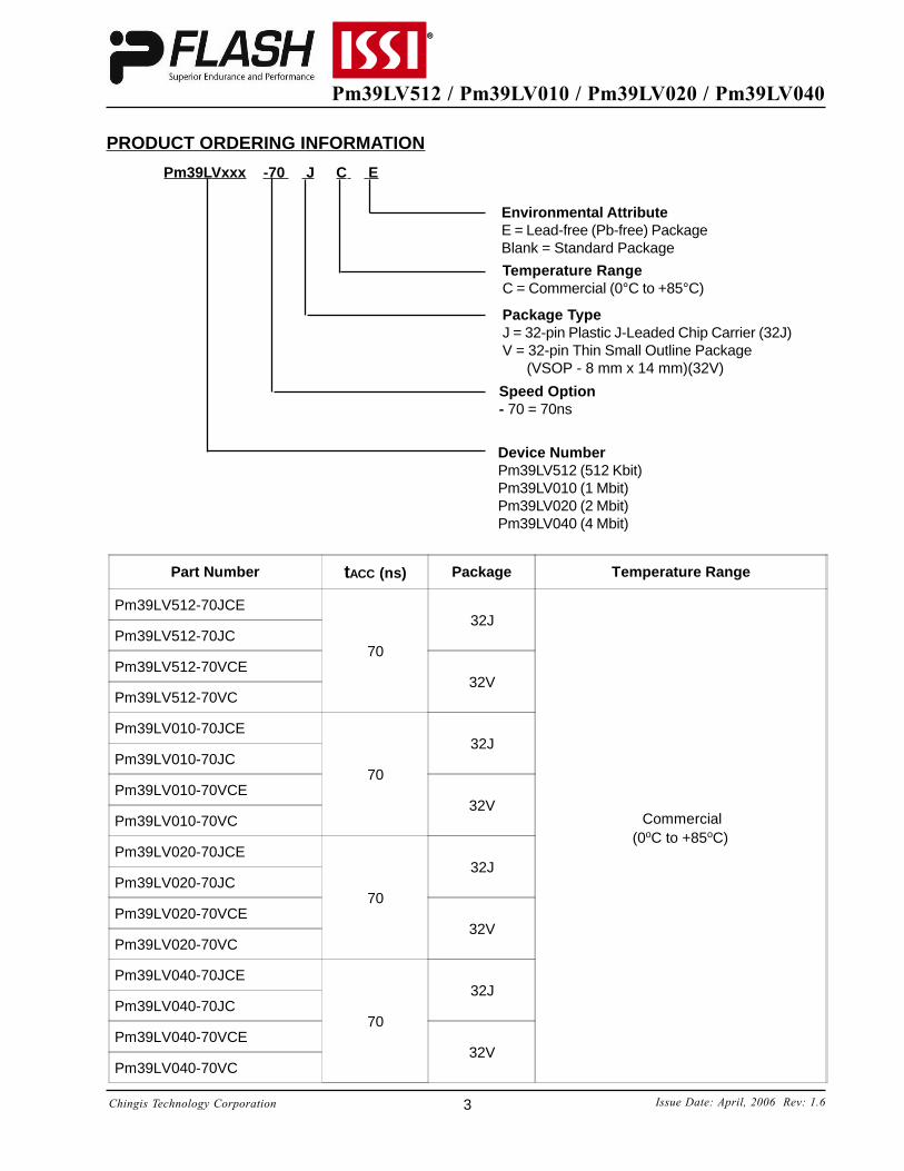
PRODUCT ORDERING INFORMATION
Pm39LVxxx -70 J C E
Temperature RangeC = Commercial (0°C to +85°C)
Package TypeJ = 32-pin Plastic J-Leaded Chip Carrier (32J)V = 32-pin Thin Small Outline Package (VSOP - 8 mm x 14 mm)(32V)
Speed Option- 70 = 70ns
Device NumberPm39LV512 (512 Kbit)Pm39LV010 (1 Mbit)Pm39LV020 (2 Mbit)Pm39LV040 (4 Mbit)
Environmental AttributeE = Lead-free (Pb-free) PackageBlank = Standard Package
Part Number tACC (ns) Package Temperature Range
Pm39LV512-70JCE
70
32J
Commercial(0oC to +85oC)
Pm39LV512-70JC
Pm39LV512-70VCE32V
Pm39LV512-70VC
Pm39LV010-70JCE
70
32JPm39LV010-70JC
Pm39LV010-70VCE32V
Pm39LV010-70VC
Pm39LV020-70JCE
70
32JPm39LV020-70JC
Pm39LV020-70VCE32V
Pm39LV020-70VC
Pm39LV040-70JCE
70
32JPm39LV040-70JC
Pm39LV040-70VCE32V
Pm39LV040-70VC
Chingis Technology Corporation Issue Date: April, 2006 Rev: 1.6
Pm39LV512 / Pm39LV010 / Pm39LV020 / Pm39LV040
4
PIN DESCRIPTIONS
SYMBOL TYPE DESCRIPTION
A0 - AMS(1) INPUT
Address Inputs: For memory addresses input. Addresses are internallylatched on the falling edge of WE# during a write cycle.
CE# INPUTChip Enable: CE# goes low activates the device's internal circuitries fordevice operation. CE# goes high deselects the device and switches intostandby mode to reduce the power consumption.
WE# INPUT Write Enable: Activate the device for write operation. WE# is active low.
OE# INPUTOutput Enable: Control the device's output buffers during a read cycle. OE#is active low.
I/O0 - I/O7INPUT/
OUTPUTData Inputs/Outputs: Input command/data during a write cycle or output dataduring a read cycle. The I/O pins float to tri-state when OE# are disabled.
VCC Device Power Supply
GND Ground
NC No Connection
Note:
1. AMS is the most significant address where AMS = A15 for Pm39LV512, A16 for Pm39LV010, A17 forPm39LV020, and A18 for Pm39LV040.
Chingis Technology Corporation Issue Date: April, 2006 Rev: 1.6
Pm39LV512 / Pm39LV010 / Pm39LV020 / Pm39LV040
5
BLOCK DIAGRAM
DEVICE OPERATION
READ OPERATION
The access of Pm39LV512/010/020/040 are similar toEPROM. To read data, three control functions must besatisfied:
• CE# is the chip enable and should be pulled low( VIL ).
• OE# is the output enable and should be pulledlow ( VIL).
• WE# is the write enable and should remains high( VIH ).
PRODUCT IDENTIFICATION
The product identification mode can be used to identifythe manufacturer and the device through hardware orsoftware read ID operation. See Table 1 for pFLASH™Manufacturer ID and Device ID. The hardware ID mode isactivated by applying a 12.0 Volt on A9 pin, typicallyused by an external programmer for selecting the rightprogramming algorithm for the devices. Refer to Table 2for Bus Operation Modes. The software ID mode is acti-vated by a three-bus-cycle command. See Table 3 forSoftware Command Definition.
W E #
CE#OE#
C O M M A N DREGISTER
CE,OE LOGIC
A0-AM S
ERASE/PROGRAMV O L T A G E
G E N E R A T O R
HIGH VOLTAGES W I T C H
I/O0-I/O7
I /O BUFFERS
DATALATCH
SENSEA M P
Y-GATING
M E M O R YARRAY
AD
DR
ES
SLA
TC
H Y -DECODER
X-DECODER
BYTE PROGRAMMING
The programming is a four-bus-cycle operation and thedata is programmed into the devices (to a logical “0”) ona byte-by-byte basis. See Table 3 for Software Com-mand Definition. A program operation is activated by writ-ing the three-byte command sequence followed by pro-gram address and one byte of program data into thedevices. The addresses are latched on the falling edgeof WE# or CE# whichever occurs later, and the data arelatched on the rising edge of WE# or CE# whicheveroccurs first. The internal control logic automaticallyhandles the internal programming voltages and timing.
A data “0” can not be programmed back to a “1”. Onlyerase operation can convert the “0”s to “1”s. The Data#Polling on I/O7 or Toggle Bit on I/O6 can be used todetect the progress or completion of a program cycle.

Chingis Technology Corporation Issue Date: April, 2006 Rev: 1.6
Pm39LV512 / Pm39LV010 / Pm39LV020 / Pm39LV040
6
DEVICE OPERATION (CONTINUED)
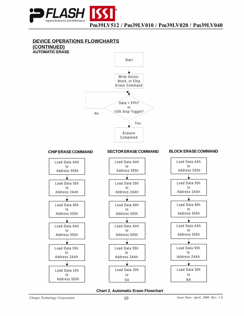
CHIP ERASE
The entire memory array can be erased through a chiperase operation. Pre-programs the devices are notrequired prior to a chip erase operation. Chip erase startsimmediately after a six-bus-cycle chip erase commandsequence. All commands will be ignored once the chiperase operation has started. The devices will return tostandby mode after the completion of chip erase.
SECTOR AND BLOCK ERASE
The memory array of Pm39LV512/010/020/040 are or-ganized into uniform 4 Kbyte sectors. A sector eraseoperation allows to erase any individual sector withoutaffecting the data in others. The memory array ofPm39LV010/020/040, excluding Pm39LV512, are alsoorganized into uniform 64 Kbyte blocks (sector group -consists of sixteen adjacent sectors). A block eraseoperation allows to erase any individual block. The sec-tor or block erase operation is similar to chip erase.
I/O7 DATA# POLLING
The Pm39LV512/010/020/040 provide a Data# Pollingfeature to indicate the progress or completion of a pro-gram and erase cycles. During a program cycle, an at-tempt to read the devices will result in the complementof the last loaded data on I/O7. Once the program op-eration is completed, the true data of the last loadeddata is valid on all outputs. During a sector, block, orchip erase cycle, an attempt to read the device will re-sult a “0” on I/O7. After the erase operation is completed,an attempt to read the device will result a “1” on I/O7.
I/O6 TOGGLE BIT
The Pm39LV512/010/020/040 also provide a Toggle Bitfeature to detect the progress or completion of a pro-gram and erase cycles. During a program or erase cycle,an attempt to read data from the device will result atoggling between “1” and “0” on I/O6. When the programor erase operation is complete, I/O6 will stop togglingand valid data will be read. Toggle bit may be accessedat any time during a program or erase cycle.
HARDWARE DATA PROTECTION
Hardware data protection protects the devices from un-intentional erase or program operation. It is performedin the following ways: (a) VCC sense: if VCC is below 1.8V (typical), the write operation is inhibited. (b) Writeinhibit: holding any of the signal OE# low, CE# high, orWE# high inhibits a write cycle. (c) Noise filter: pulsesof less than 5 ns (typical) on the WE# or CE# input willnot initiate a write operation.
Product Identification Data
Manufacturer ID 9Dh
Device ID:
Pm39LV512 1Bh
Pm39LV010 1Ch
Pm39LV020 3Dh
Pm39LV040 3Eh
Table 1. Product Identification

Chingis Technology Corporation Issue Date: April, 2006 Rev: 1.6
Pm39LV512 / Pm39LV010 / Pm39LV020 / Pm39LV040
7
Memory Density Block (1) Block Size(Kbytes)
SectorSector Size
(Kbytes)Address Range
512Kbit
1 Mbit
2 Mbit
4 Mbit
Block 0 (2) 64
Sector 0 4 00000h - 00FFFh
Sector 1 4 01000h - 01FFFh
: : :
Sector 15 4 0F000h - 0FFFFh
Block 1 64
Sector 16 4 10000h - 10FFFh
Sector 17 4 11000h - 11FFFh
: : :
Sector 31 4 1F000h - 1FFFFh
Block 2 64 " " 20000h - 2FFFFh
Block 3 64 " " 30000h - 3FFFFh
Block 4 64 " " 40000h - 4FFFFh
Block 5 64 " " 50000h - 5FFFFh
Block 6 64 " " 60000h - 6FFFFh
Block 7 64 " " 70000h - 7FFFFh
SECTOR/BLOCK ADDRESS T ABLE
Notes:
1. A Block is a 64 Kbyte sector group which consists of sixteen adjecent sectors of 4 Kbyte each.
2. Block erase feature is available for Pm39LV010/020/040 only. The chip erase command should be used toerase the Block 0 for the Pm39LV512.
Chingis Technology Corporation Issue Date: April, 2006 Rev: 1.6
Pm39LV512 / Pm39LV010 / Pm39LV020 / Pm39LV040
8
COMMAND DEFINITION
Table 3. Software Command Definition
CommandSequence
BusCycle
1st BusCycle
Addr Data
2nd BusCycle
Addr Data
3rd BusCycle
Addr Data
4th BusCycle
Addr Data
5th BusCylce
Addr Data
6th BusCycle
Addr Data
Read 1 Addr DOUT
Chip Erase 6 555h AAh 2AAh 55h 555h 80h 555h AAh 2AAh 55h 555h 10h
Sector Erase 6 555h AAh 2AAh 55h 555h 80h 555h AAh 2AAh 55h SA (1) 30h
Block Erase 6 555h AAh 2AAh 55h 555h 80h 555h AAh 2AAh 55h BA (2) 50h
Byte Program 4 555h AAh 2AAh 55h 555h A0h Addr DIN
Product ID Entry 3 555h AAh 2AAh 55h 555h 90h
Product ID Exit (3) 3 555h AAh 2AAh 55h 555h F0h
Product ID Exit (3) 1 XXXh F0h
Notes:1. SA = Sector address of the sector to be erased.2. BA = Block address of the block to be erased.3. Either one of the Product ID Exit command can be used.
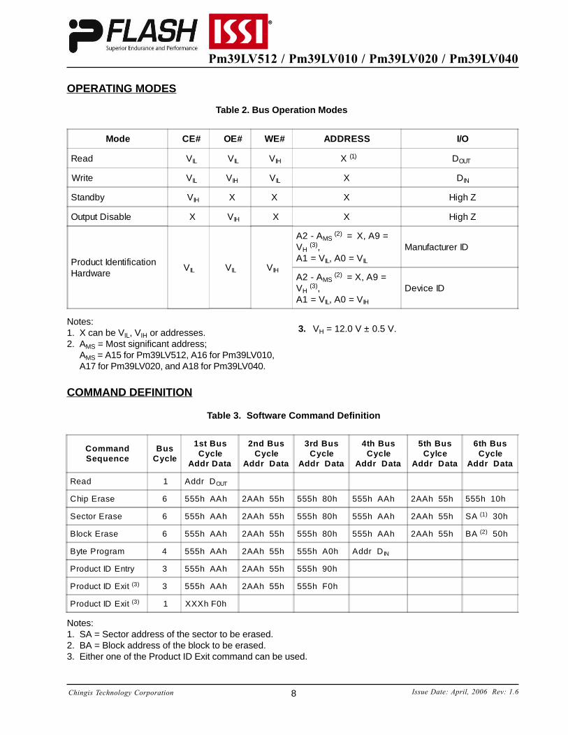
OPERATING MODES
Notes:1. X can be VIL, VIH or addresses.2. AMS = Most significant address;
AMS = A15 for Pm39LV512, A16 for Pm39LV010,A17 for Pm39LV020, and A18 for Pm39LV040.
Table 2. Bus Operation Modes
Mode CE# OE# WE# ADDRESS I/O
Read VIL VIL VIH X (1) DOUT
Write VIL VIH VIL X DIN
Standby VIH X X X High Z
Output Disable X VIH X X High Z
Product IdentificationHardware
VIL VIL VIH
A2 - AMS (2)
= X, A9 =VH (3),A1 = VIL, A0 = VIL
Manufacturer ID
A2 - AMS (2)
= X, A9 =VH (3),A1 = VIL, A0 = VIH
Device ID
3. VH = 12.0 V ± 0.5 V.

Chingis Technology Corporation Issue Date: April, 2006 Rev: 1.6
Pm39LV512 / Pm39LV010 / Pm39LV020 / Pm39LV040
9
DEVICE OPERATIONS FLOWCHARTS
AUTOMATIC PROGRAMMING
Chart 1. Automatic Programming Flowchart
Start
Load Data AAhto
Address 555H
Load Data 55hto
Address 2AAh
Load Data A0hto
Address 555h
Load ProgramData to
Program Address
I /O7 = Data?or
I /O6 Stop Toggle?
Last Address?
Prog rammingComple ted
N o
N o
Yes
Yes
AddressIncrement
Chingis Technology Corporation Issue Date: April, 2006 Rev: 1.6
Pm39LV512 / Pm39LV010 / Pm39LV020 / Pm39LV040
10
AUTOMATIC ERASE
Chart 2. Automatic Erase Flowchart
DEVICE OPERATIONS FLOWCHARTS(CONTINUED)
Start
Wr i te Sector ,Block, or Chip
E rase Command
Data = FFh?or
I /O6 Stop Toggle?
ErasureComple ted
Yes
N o
SECTOR ERASE COMMAND
Load Data AAhto
Address 555h
Load Data 55hto
Address 2AAh
Load Data 80hto
Address 555h
Load Data AAhto
Address 555h
Load Data 55hto
Address 2AAh
Load Data 10hto
Address 555h
Load Data AAhto
Address 555h
Load Data 55hto
Address 2AAh
Load Data 80hto
Address 555h
Load Data AAhto
Address 555h
Load Data 55hto
Address 2AAh
Load Data 30hto
S A
CHIP ERASE COMMAND BLOCK ERASE COMMAND
Load Data AAhto
Address 555h
Load Data 55hto
Address 2AAh
Load Data 80hto
Address 555h
Load Data AAhto
Address 555h
Load Data 55hto
Address 2AAh
Load Data 50hto
B A

Chingis Technology Corporation Issue Date: April, 2006 Rev: 1.6
Pm39LV512 / Pm39LV010 / Pm39LV020 / Pm39LV040
11
SOFTWARE PRODUCT IDENTIFICATION EXIT
Load Data AAhto
Address 555h
Load Data 55hto
Address 2AAh
Load Data 90hto
Address 555h
Enter ProductIdent i f icat ion
Mode (1,2)
Load Data AAhto
Address 555h
Load Data 55hto
Address 2AAh
Load Data F0hto
Address 555h
Exi t ProductIdent i f icat ion
Mode (3)
Load Data F0hto
Address XXXh
Exi t ProductIdent i f icat ion
Mode (3)
or
Chart 3. Software Product Identification Entry/Exit Flowchart
SOFTWARE PRODUCT IDENTIFICATION ENTRY
DEVICE OPERATIONS FLOWCHARTS(CONTINUED)
Notes:1. The device will enter Product Identification mode after excuting the Product ID Entry command.2. Under Product Identification mode, the Manufacturer ID and Device ID of devices can be read at address
X0000h and X0001h where X = Don’t Care.3. The device returns to standby operation.

Chingis Technology Corporation Issue Date: April, 2006 Rev: 1.6
Pm39LV512 / Pm39LV010 / Pm39LV020 / Pm39LV040
12
DC AND AC OPERATING RANGE
ABSOLUTE MAXIMUM RA TINGS (1)
Notes:1. Stresses under those listed in “Absolute Maximum Ratings” may cause permanent damage
to the device. This is a stress rating only. The functional operation of the device or any otherconditions under those indicated in the operational sections of this specification is notimplied. Exposure to absolute maximum rating condition for extended periods may affecteddevice reliability.
2. Maximum DC voltage on input or I/O pins are VCC + 0.5 V. During voltage transitioningperiod, input or I/O pins may overshoot to VCC + 2.0 V for a period of time up to 20 ns.Minimum DC voltage on input or I/O pins are -0.5 V. During voltage transitioning period,input or I/O pins may undershoot GND to -2.0 V for a period of time up to 20 ns.
3. Maximum DC voltage on A9 pin is +13.0 V. During voltage transitioning period, A9 pin mayovershoot to +14.0 V for a period of time up to 20 ns. Minimum DC voltage on A9 pin is -0.5V. During voltage transitioning period, A9 pin may undershoot GND to -2.0 V for a period oftime up to 20 ns.
Temperature Under Bias -65oC to +125oC
Storage Temperature
Surface Mount Lead Soldering TemperatureStandard Package 240oC 3 Seconds
Lead-free Package 260oC 3 Seconds
Input Voltage with Respect to Ground on All Pins except A9 pin(2) -0.5 V to VCC + 0.5 V
Input Voltage with Respect to Ground on A9 pin(3) -0.5 V to +13.0 V
All Output Voltage with Respect to Ground -0.5 V to VCC + 0.5 V
VCC(2) -0.5 V to +6.0 V
-65oC to +125oC
Part Number Pm39LV512/010/020/040
Operating Temperature 0oC to +85oC
Vcc Power Supply 2.7 V - 3.6 V

Chingis Technology Corporation Issue Date: April, 2006 Rev: 1.6
Pm39LV512 / Pm39LV010 / Pm39LV020 / Pm39LV040
13
DC CHARACTERISTICS
READ OPERATIONS CHARACTERISTICS
AC CHARACTERISTICS
Note: 1. Characterized but not 100% tested.
Symbol Parameter Condition Min Typ Max Units
ILI Input Load Current VIN= 0 V to V CC 1 µA
ILO Output Leakage Current VI/O = 0 V to V CC 1
ISB1 VCC Standby Current CMOS CE#, OE# = V CC ?0.3 V 0.1 5
ISB2 VCC Standby Current TTL CE# = V IH to VCC 0.05 3 mA
ICC1 VCC Active Read Current f = 5 MHz; IOUT = 0 mA 4 15 mA
ICC2(1) VCC Program/Erase Current 8 20 mA
VIL Input Low Voltage -0.5 0.8 V
VIH Input High Voltage 0.7 VCC VCC + 0.3 V
VOL Output Low VoltageIOL = 2.1 mA; VCC = VCC
min0.45 V
VOH Output High VoltageIOH = -100 µA; VCC = VCC
minVCC - 0.2 V
µA
µA
Symbol Parameter
Pm39LV512-55Pm39LV010-55Pm39LV020-55Pm39LV040-55
Pm39LV512-70Pm39LV010-70Pm39LV020-70Pm39LV040-70
Units
Min Max Min Max
tRC Read Cycle Time 55 70 ns
tACC Address to Output Delay 55 70 ns
tCE CE# to Output Delay 55 70 ns
tOE OE# to Output Delay 30 35 ns
tDF CE# or OE# to Output High Z 0 15 0 25 ns
tOHOutput Hold from OE#, CE# orAddress, whichever occured first
0 0 ns
tVCS VCC Set-up Time 50 50 µs

Chingis Technology Corporation Issue Date: April, 2006 Rev: 1.6
Pm39LV512 / Pm39LV010 / Pm39LV020 / Pm39LV040
14
READ OPERATIONS AC WAVEFORMS
OUTPUT TEST LOAD INPUT TEST WAVEFORMS
AND MEASUREMENT LEVEL
AC CHARACTERISTICS (CONTINUED)
PIN CAPACITANCE ( f = 1 MHz, T = 25°C )
Typ Max Units Conditions
CIN 4 6 pF VIN = 0 V
COUT 8 12 pF VOUT = 0 V
Note: These parameters are characterized but not 100% tested.
ADDRESS VALID
tRC
tACCtCE
tOE
tDF
tOH
O U T P U TVALID
HIGH Z
A D D R E S S
CE#
OE#
W E #
O U T P U T
V C C
tVCS
3.3 V
1.8 K
1.3 K
OUTPUT PIN
C L = 30 pF
3.0 V
0.0 V
1.5 VA CMeasuremen tLevel
Input

Chingis Technology Corporation Issue Date: April, 2006 Rev: 1.6
Pm39LV512 / Pm39LV010 / Pm39LV020 / Pm39LV040
15
WRITE (PROGRAM/ERASE) OPERATIONS CHARACTERISTICS
AC CHARACTERISTICS (CONTINUED)
PROGRAM OPERATIONS AC WAVEFORMS - WE# CONTROLLED
tCH
tCS
tW P tW P HtBP
tDHtDS
tAH
tAS
555 555 A D D R E S S2AA
AA 55 A0 INPUTDATA
VALIDDATA
DATA IN
A0 - A M S
O E #
W E #
CE#
Program Cycle
tW C
V CC
tVCS
Symbol Parameter
Pm39LV512-55Pm39LV010-55Pm39LV020-55Pm39LV040-55
Pm39LV512-70Pm39LV010-70Pm39LV020-70Pm39LV040-70 Units
Min Max Min Max
tWC Write Cycle Time 55 70 ns
tAS Address Set-up Time 0 0 ns
tAH Address Hold Time 30 30 ns
tCS CE# and WE# Set-up Time 0 0 ns
tCH CE# and WE# Hold Time 0 0 ns
tOEH OE# High Hold Time 10 10 ns
tDS Data Set-up Time 40 40 ns
tDH Data Hold Time 0 0 ns
tWP Write Pulse Width 35 35 ns
tWPH Write Pulse Width High 20 20 ns
tBP Byte Programming Time 20 20
tEC Chip or Block Erase Time 100 100 ms
tVCS VCC Set-up Time 50 50 µs
µs

Chingis Technology Corporation Issue Date: April, 2006 Rev: 1.6
Pm39LV512 / Pm39LV010 / Pm39LV020 / Pm39LV040
16
AC CHARACTERISTICS (CONTINUED)
CHIP ERASE OPERATIONS AC WAVEFORMS
tCH
tCS
tW P tW P HtBP
tDHtDS
tAH
tAS
555 555 A D D R E S S2 A A
A A 55 A 0 INPUTD A T A
VALIDD A T A
DATA IN
A0 - AM S
O E #
W E #
C E #
Program Cyc le
tW C
V C C
tVCS
PROGRAM OPERATIONS AC WAVEFORMS - CE# CONTROLLED
A A 55 55 1080 A A
555 2 A A 555 555 2 A A
tEC
tW P HtW P
tAS tAH tDH
tDS
AO - AM S
W E #
C E #
O E #
DATA IN
tW C
555
V C C
tVCS

Chingis Technology Corporation Issue Date: April, 2006 Rev: 1.6
Pm39LV512 / Pm39LV010 / Pm39LV020 / Pm39LV040
17
SECTOR OR BLOCK ERASE OPERATIONS AC WAVEFORMS
A A 55 55 30 or 5080 A A
555 2 A A 555 555 2 A A Sector or BlockAddress
tEC
tW P HtW P
tAS tAH tDH
tDS
AO - AM S
W E #
C E #
O E #
DATA IN
tW C
V C C
tVCS
TOGGLE BIT AC WAVEFORMS
AC CHARACTERISTICS (CONTINUED)
tOEH
W E #
C E #
O E #
I /O6 T O G G L ES T O P
T O G G L I N GVALIDD A T A
tO E
T O G G L ED A T A
tDF
tO H
Note: Toggling CE#, OE#, or both OE# and CE# will operate Toggle Bit.

Chingis Technology Corporation Issue Date: April, 2006 Rev: 1.6
Pm39LV512 / Pm39LV010 / Pm39LV020 / Pm39LV040
18
DATA# POLLING AC WAVEFORMS
AC CHARACTERISTICS (CONTINUED)
Note: Toggling CE#, OE#, or both OE# and CE# will operate Data# Polling.
PROGRAM/ERASE PERFORMANCE
tCH tCE
tOEH
tOE
tDF
tOH
VALID DATAI/O7#
W E #
CE#
OE#
I/O7
Parameter Unit Typ Max Remarks
Sector Erase Time ms 55 100 From writing erase command to erase completion
Block Erase Time ms 55 100 From writing erase command to erase completion
Chip Erase Time ms 55 100 From writing erase command to erase completion
Byte Programming Time µs 16 20Excludes the time of four-cycle program commandexecution
Parameter Min Typ Unit Test Method
Endurance 100,000 (2) Cycles JEDEC Standard A117
Data Retention 20 Years JEDEC Standard A103
ESD - Human Body Model 2,000 Volts JEDEC Standard A114
ESD - Machine Model 200 Volts JEDEC Standard A115
Latch-Up 100 + ICC1 mA JEDEC Standard 78
Note: These parameters are characterized but not 100% tested.
Note: 1. These parameters are characterized but not 100% tested.2. Preliminary specification only and will be formalized after cycling qualification test.
RELIABILITY CHARACTERISTICS (1)
Chingis Technology Corporation Issue Date: April, 2006 Rev: 1.6
Pm39LV512 / Pm39LV010 / Pm39LV020 / Pm39LV040
19
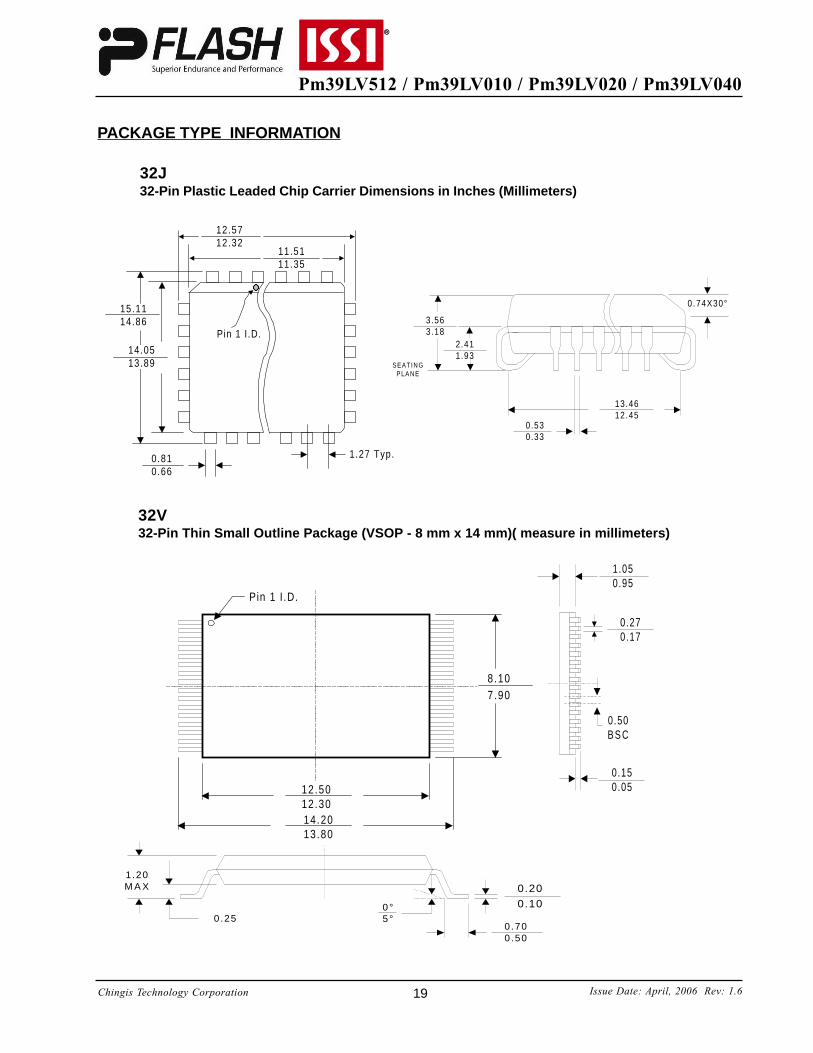
PACKAGE TYPE INFORMA TION
32V32-Pin Thin Small Outline Package (VSOP - 8 mm x 14 mm)( measure in millimeters)
32J32-Pin Plastic Leaded Chip Carrier Dimensions in Inches (Millimeters)
Pin 1 I.D.
15.1114.86
14.0513.89
1.27 Typ.0.810.66
11.5111.35
12.5712.32
0.74X30°
13.4612.45
0.530.33
2.411.93
3.563.18
SEATINGP L A N E
0.50B S C
1.050.95
0.270.17
0.150.05
Pin 1 I .D.
12.5012.3014.2013.80
8.107.90
1.20M A X
0.250°5°
0.200.10
0.700.50

Chingis Technology Corporation Issue Date: April, 2006 Rev: 1.6
Pm39LV512 / Pm39LV010 / Pm39LV020 / Pm39LV040
20
REVISION HISTORY
Date Revision No. Description of Changes Page No.
May, 2003 1.0 Preliminary Information All
September, 2003 1.1 Updated program description and formal release 5
December, 2003 1.2
Added Lead-free package option 1, 3, 12
Upgraded guranteed program/erase cycles from50,000 to 100,000 (preliminary)
1, 18
Revised output test load as 30 pF for all speed 14
Revised package dimension information 19
March, 2004 1.3 Extend the operation range of temperature All
June, 2005 1.4 Improve tBP (max) from 30us to 20us 15, 18
March, 2006 1.5 Change Logo and company name All
April, 2006 1.6 Correct logo for some description 3, 5


![Conditions de tests pour le raccordement d’équipements ... · RA mode US AT_INIT AT_INIT AT_INIT AT_INIT AT_INIT Min bitrate US [kbit/s] 600 600 600 600 600 Max bitrate US [kbit/s]](https://img.pdfslide.fr/doc/110x75/5ea923b63f208d3cf14cb6b0/conditions-de-tests-pour-le-raccordement-daquipements-ra-mode-us-atinit.jpg)