Embed Size (px)
Citation preview
Bull. Mater. Sci. (2019) 42:33 © Indian Academy of Scienceshttps://doi.org/10.1007/s12034-018-1711-2
Active area cell efficiency (19%) monocrystalline silicon solar cellfabrication using low-cost processing with small footprintlaboratory tools
PRABIR K BASU1,2,∗, SANDEEP KUMBHAR1, K P SREEJITH1,3, TARUN S YADAV1,3,ANIL KOTTANTHARAYIL1,3, B M ARORA1, K L NARASIMHAN1 and ASHOK K SHARMA1
1National Centre for Photovoltaic Research and Education (NCPRE), Mumbai 400076, India2Solar Energy Research Institute of India (SERIS), National University of Singapore, Singapore 117574, Singapore3Department of Electrical Engineering, Indian Institute of Technology Bombay, Powai, Mumbai 400076, India∗Author for correspondence ([email protected])
MS received 28 March 2018; accepted 12 July 2018; published online 2 February 2019
Abstract. A high efficiency (>18%) industrial large area crystalline silicon wafer solar cell fabrication process generallyrequires industrial equipment with large footprint, high capital and running costs. Stricter processing window, continuousmonitoring and automated functioning are the reasons for it. However, for any conventional laboratory (lab) it is alwaysdifficult to manage these requirements with limited available lab space or insufficient fund and other related resources. In thiswork, we report a novel way to fabricate high efficiency full area aluminium back surface field monocrystalline silicon wafersolar cells in our lab using low-cost processing with small-footprint fabrication tools for 6 inch pseudo-square industrialwafers. The novelty of our work includes optimization of every fabrication process step, e.g., texturization, emitter diffusion,emitter passivation and anti-reflection coating deposition, edge-isolation, screen printing and co-firing individually. Thesemodifications include tuning of processing tools and processes, utility changes and inclusion of additional process steps.Beaker-based chemical processes, manual diffusion furnace, introduction of low temperature oxidation, low temperaturesilicon nitride deposition processes, plasma-edge isolation tool, single manual screen printer, single oven drying of metalpastes and co-firing using rapid thermal processing tools were used at our lab. For our cells, actual and active area efficienciesof 18.5 and 19% (measured under AM1.5G 1 Sun condition), respectively, were achieved.
Keywords. Limited laboratory space; small-footprint processing equipment; low-cost processing; individually optimizedprocesses; high-cell efficiency.
1. Introduction
The present global photovoltaic (PV) market is dominatedby crystalline silicon (Si) wafer solar cells [1]. This domina-tion of crystalline Si necessitates more research to increasethe energy conversion efficiency of Si wafer solar cells ina cost-effective way. This ultimately results in worldwiderapid developmental works in many laboratories in this areaof PV. However, initiation of any experimental works ofthe fabrication of industrial size monocrystalline Si (c-Si)wafer solar cells requires a laboratory (lab) with all spe-cialized processing equipment. A conventional Si wafer cellfabrication process requires optical engineering by chemi-cal texturization, junction formation by diffusion, the edge orrear side Si etching for parasitic junction removal, passiva-tion and anti-reflection coating (ARC) deposition by plasmaenhanced chemical vapour deposition (PECVD), metal pastedeposition by screen printing and finally, co-firing of metalcontacts in a belt furnace [2]. During texturization, ran-dom but uniform pyramids [3] formed on the Si surface toreduce surface reflectance and low-cost alkaline texturing is
widely used for texturization of c-Si wafers. Present day Sicells have uniform and shallow pn junction of ∼0.2–0.3 µmjunction depth over the entire 6 inch pseudo or full squarewafer area [4]. Removal of the junction from the rear side,or edges, or both, of the diffused wafer is a critical step toenhance cell open circuit voltage (Voc) by minimizing thecell shunt resistance (Rsh) [2]. The emitter surface passiva-tion layer has dual requirement. It should act as an ARC layerto improve cell short circuit current (Isc). It must also act asa passivating layer to improve cell Voc [5]. The passivated Siwafers need to be metallized by screen printing of suitablemetal pastes, i.e., silver (Ag) paste on an emitter and alu-minium (Al) paste on the rear side, followed by a drying andco-firing process to complete the cell fabrication sequence.
The standard equipment involved in the cell fabricationis wet chemical benches, diffusion furnaces, chemical edgeisolation tools, PECVD systems, screen printers, belt driersand belt firing furnaces. These tools normally require largespace to accommodate them in the lab and additionally somemore space for respective chemical/gas delivery and disposalsystems. Besides their large footprint, industrial equipment
1
33 Page 2 of 11 Bull. Mater. Sci. (2019) 42:33
Table 1. Footprint of individual tools used for cell fabrication at the NCPRE lab.
Tool Process Tool make and model no. Quantity Footprint (m2)
Wet chemical bench Texturization, otherchemical processes
Locally made with whitePP sheet
One 1.6
High temperature quartz furnace Diffusion, oxidation Protemp, Sirius PRO 200 One 2.7PECVD Passivation and ARC
amorphous SiNx
deposition
Oxford Instruments,Plasmalab System 100
One 3.0
Plasma tool Edge isolation BSET EQ, NT-2 One 1.1Screen printer Printing of Al and Ag
metal pastesHaiku Tech, P200S One 1.3
Convention oven Drying of Al and Agpastes after printing
Locally made One 0.8
Firing furnace RTP furnace for fast firingof metals
Allwin21 Corp., AW 610 One 2.0
needs essentially high capital and running costs to producehigh-efficiency cells. However, in any conventional researchlab, both space constraints and low budget (compared withindustry) prevail. This way initiation of any fabricationoriented research on Si wafer solar cells becomesunfeasible.
The Si solar cell lab at National Centre for PhotovoltaicResearch and Education (NCPRE), c-Si cell fabrication facil-ity has an area of 160 m2 with small-footprint equipment. Thetools include manual wet bench for hosting all the chemicalprocesses with glass beakers and manual controls, semi-automatic diffusion furnace with manual gas-flow and exhaustunits, single wafer PECVD system with substrate heatingup to 380◦C, plasma-edge isolation, single semi-automaticscreen-printer with manual alignment, single convection ovendrier and finally a rapid thermal processing (RTP) metal co-firing tool. These tools cannot be compared with sophisticatedindustrial tools, e.g., inline or batch-based automatic wetbenches for chemical processing, large fully automatic dif-fusion furnace, inline chemical rear-junction isolation bench,inline/tube-based PECVD system with substrate heating upto 450◦C, auto-aligned high-resolution screen-printers eachfor separate metal printing, separate conveyer-based driersassociated with individual screen printers and fast-firing beltfurnace contact formation system [2] either cost-wise or infootprint.
Our present work reports the high efficiency cellfabrication process within the lab constraints in a smalllab space. The optimization and modifications of each pro-cess, processing tools, utilities and accessories to achievethe best possible fabrication conditions on 6 inch pseudo-square Cz p-type c-Si wafers are discussed in detail alongwith their characterization results. The new process wasapplied to fabricate industrial-grade, screen-printed solar cellsto produce actual power conversion efficiencies of 18.5%in our NCPRE cell fabrication lab measured under STCconditions.
2. Experimental
2.1 Fabrication tool footprints
The footprints of individual tools used for cell fabricationin our lab are listed in table 1. Among the tools, area-wise largest tools are our diffusion and PECVD tools with∼3 m2 area. However, these tools are still much smaller thanany industrial or pilot line tools. Also, sufficient workingspace is still available after placing all these tools inside thelab.
2.2 Cell fabrication
In the present work, the texturing was performed on adiamond-wire-sawn (DWS) as-cut industrial grade Cz c-Siwafers (6 inch pseudo-square, boron doped, p-type, (100) ori-entation, ∼1.5–2.5� cm resistivity, 160–180 µm thickness)by using a novel texturing process [6]. Our process com-bines a novel single step low-cost saw damage removal (SDR)solution of potassium hydroxide (KOH)–sodium hypochlo-rite (NaOCl) [6], followed by pyramidal texturing using KOH,potassium silicate (K2SiO3) and isopropyl alcohol (IPA) solu-tion [3]. Textured wafers were diffused for a target sheetresistance (Rsq) of 80 � sq−1 in a tube diffusion furnace(Protemp USA, Sirius PRO 200) using a liquid phospho-rus oxychloride (POCl3) dopant source for phosphorous (P)diffusion. After dipping in a 2% hydrofluoric acid (HF) solu-tion for phosphosilicate glass (PSG) removal, the wafers wereoxidized to form silicon dioxide (SiO2) in a low temperaturethermal oxidation (LTO) process in the same furnace for 1 h at600◦C. Amorphous silicon nitride (SiNx ) passivation (whichalso acts as an ARC layer) was then deposited by PECVDusing an Oxford Instruments, Plasmalab System 100 tool at380◦C. The deposited SiNx film has a refractive index of 2.00(at 633 nm) and a thickness of 90 nm as measured on our
Bull. Mater. Sci. (2019) 42:33 Page 3 of 11 33
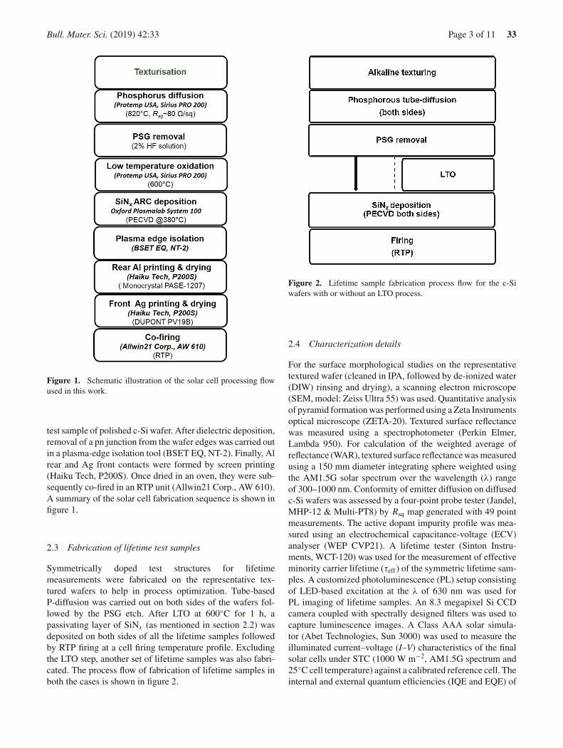
Figure 1. Schematic illustration of the solar cell processing flowused in this work.
test sample of polished c-Si wafer. After dielectric deposition,removal of a pn junction from the wafer edges was carried outin a plasma-edge isolation tool (BSET EQ, NT-2). Finally, Alrear and Ag front contacts were formed by screen printing(Haiku Tech, P200S). Once dried in an oven, they were sub-sequently co-fired in an RTP unit (Allwin21 Corp., AW 610).A summary of the solar cell fabrication sequence is shown infigure 1.
2.3 Fabrication of lifetime test samples
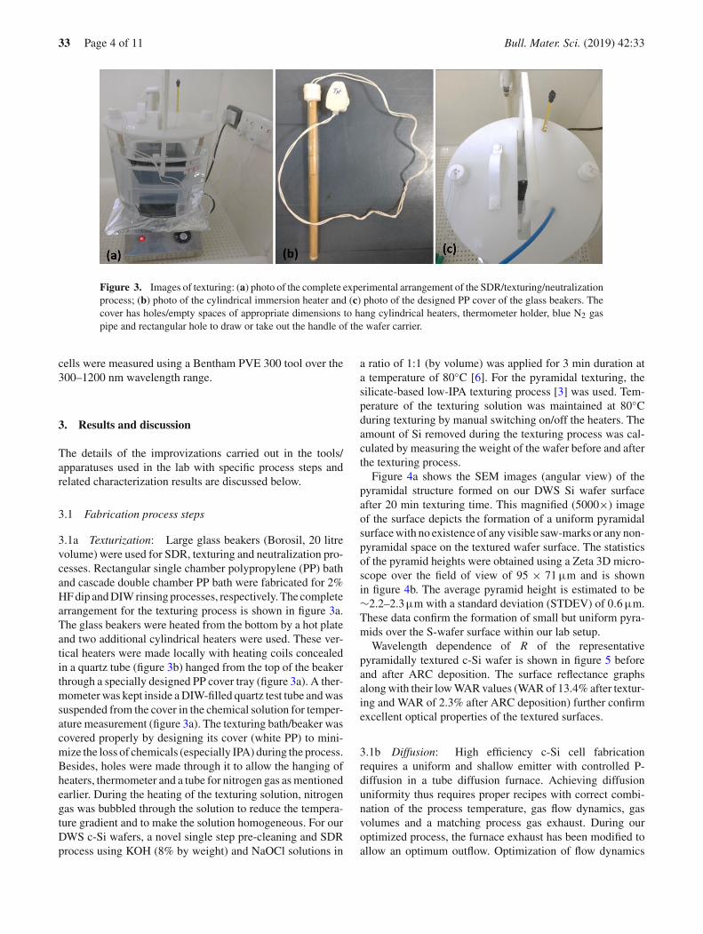
Symmetrically doped test structures for lifetimemeasurements were fabricated on the representative tex-tured wafers to help in process optimization. Tube-basedP-diffusion was carried out on both sides of the wafers fol-lowed by the PSG etch. After LTO at 600◦C for 1 h, apassivating layer of SiNx (as mentioned in section 2.2) wasdeposited on both sides of all the lifetime samples followedby RTP firing at a cell firing temperature profile. Excludingthe LTO step, another set of lifetime samples was also fabri-cated. The process flow of fabrication of lifetime samples inboth the cases is shown in figure 2.
Figure 2. Lifetime sample fabrication process flow for the c-Siwafers with or without an LTO process.
2.4 Characterization details
For the surface morphological studies on the representativetextured wafer (cleaned in IPA, followed by de-ionized water(DIW) rinsing and drying), a scanning electron microscope(SEM, model: Zeiss Ultra 55) was used. Quantitative analysisof pyramid formation was performed using a Zeta Instrumentsoptical microscope (ZETA-20). Textured surface reflectancewas measured using a spectrophotometer (Perkin Elmer,Lambda 950). For calculation of the weighted average ofreflectance (WAR), textured surface reflectance was measuredusing a 150 mm diameter integrating sphere weighted usingthe AM1.5G solar spectrum over the wavelength (λ) rangeof 300–1000 nm. Conformity of emitter diffusion on diffusedc-Si wafers was assessed by a four-point probe tester (Jandel,MHP-12 & Multi-PT8) by Rsq map generated with 49 pointmeasurements. The active dopant impurity profile was mea-sured using an electrochemical capacitance-voltage (ECV)analyser (WEP CVP21). A lifetime tester (Sinton Instru-ments, WCT-120) was used for the measurement of effectiveminority carrier lifetime (τeff ) of the symmetric lifetime sam-ples. A customized photoluminescence (PL) setup consistingof LED-based excitation at the λ of 630 nm was used forPL imaging of lifetime samples. An 8.3 megapixel Si CCDcamera coupled with spectrally designed filters was used tocapture luminescence images. A Class AAA solar simula-tor (Abet Technologies, Sun 3000) was used to measure theilluminated current–voltage (I–V) characteristics of the finalsolar cells under STC (1000 W m−2, AM1.5G spectrum and25◦C cell temperature) against a calibrated reference cell. Theinternal and external quantum efficiencies (IQE and EQE) of
33 Page 4 of 11 Bull. Mater. Sci. (2019) 42:33
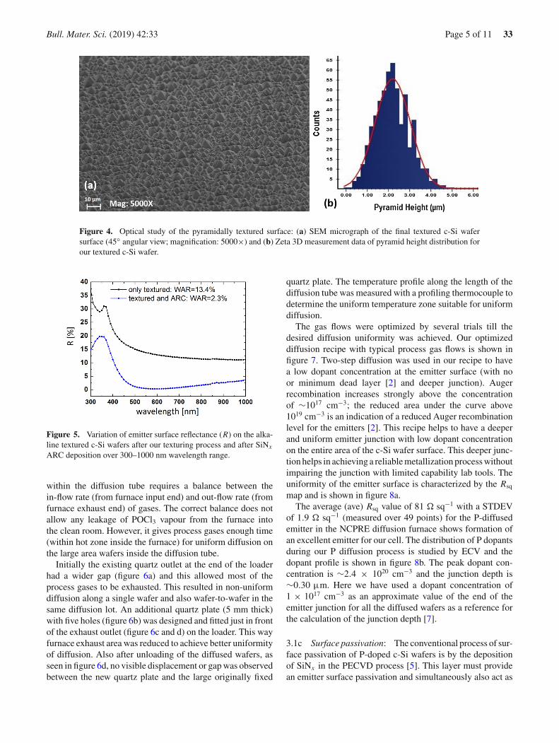
Figure 3. Images of texturing: (a) photo of the complete experimental arrangement of the SDR/texturing/neutralizationprocess; (b) photo of the cylindrical immersion heater and (c) photo of the designed PP cover of the glass beakers. Thecover has holes/empty spaces of appropriate dimensions to hang cylindrical heaters, thermometer holder, blue N2 gaspipe and rectangular hole to draw or take out the handle of the wafer carrier.
cells were measured using a Bentham PVE 300 tool over the300–1200 nm wavelength range.
3. Results and discussion
The details of the improvizations carried out in the tools/apparatuses used in the lab with specific process steps andrelated characterization results are discussed below.
3.1 Fabrication process steps
3.1a Texturization: Large glass beakers (Borosil, 20 litrevolume) were used for SDR, texturing and neutralization pro-cesses. Rectangular single chamber polypropylene (PP) bathand cascade double chamber PP bath were fabricated for 2%HF dip and DIW rinsing processes, respectively. The completearrangement for the texturing process is shown in figure 3a.The glass beakers were heated from the bottom by a hot plateand two additional cylindrical heaters were used. These ver-tical heaters were made locally with heating coils concealedin a quartz tube (figure 3b) hanged from the top of the beakerthrough a specially designed PP cover tray (figure 3a). A ther-mometer was kept inside a DIW-filled quartz test tube and wassuspended from the cover in the chemical solution for temper-ature measurement (figure 3a). The texturing bath/beaker wascovered properly by designing its cover (white PP) to mini-mize the loss of chemicals (especially IPA) during the process.Besides, holes were made through it to allow the hanging ofheaters, thermometer and a tube for nitrogen gas as mentionedearlier. During the heating of the texturing solution, nitrogengas was bubbled through the solution to reduce the tempera-ture gradient and to make the solution homogeneous. For ourDWS c-Si wafers, a novel single step pre-cleaning and SDRprocess using KOH (8% by weight) and NaOCl solutions in
a ratio of 1:1 (by volume) was applied for 3 min duration ata temperature of 80◦C [6]. For the pyramidal texturing, thesilicate-based low-IPA texturing process [3] was used. Tem-perature of the texturing solution was maintained at 80◦Cduring texturing by manual switching on/off the heaters. Theamount of Si removed during the texturing process was cal-culated by measuring the weight of the wafer before and afterthe texturing process.
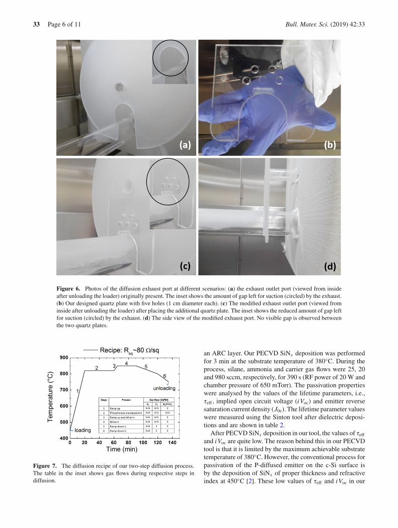
Figure 4a shows the SEM images (angular view) of thepyramidal structure formed on our DWS Si wafer surfaceafter 20 min texturing time. This magnified (5000×) imageof the surface depicts the formation of a uniform pyramidalsurface with no existence of any visible saw-marks or any non-pyramidal space on the textured wafer surface. The statisticsof the pyramid heights were obtained using a Zeta 3D micro-scope over the field of view of 95 × 71µm and is shownin figure 4b. The average pyramid height is estimated to be∼2.2–2.3µm with a standard deviation (STDEV) of 0.6µm.These data confirm the formation of small but uniform pyra-mids over the S-wafer surface within our lab setup.
Wavelength dependence of R of the representativepyramidally textured c-Si wafer is shown in figure 5 beforeand after ARC deposition. The surface reflectance graphsalong with their low WAR values (WAR of 13.4% after textur-ing and WAR of 2.3% after ARC deposition) further confirmexcellent optical properties of the textured surfaces.
3.1b Diffusion: High efficiency c-Si cell fabricationrequires a uniform and shallow emitter with controlled P-diffusion in a tube diffusion furnace. Achieving diffusionuniformity thus requires proper recipes with correct combi-nation of the process temperature, gas flow dynamics, gasvolumes and a matching process gas exhaust. During ouroptimized process, the furnace exhaust has been modified toallow an optimum outflow. Optimization of flow dynamics
Bull. Mater. Sci. (2019) 42:33 Page 5 of 11 33
Figure 4. Optical study of the pyramidally textured surface: (a) SEM micrograph of the final textured c-Si wafersurface (45◦ angular view; magnification: 5000×) and (b) Zeta 3D measurement data of pyramid height distribution forour textured c-Si wafer.
Figure 5. Variation of emitter surface reflectance (R) on the alka-line textured c-Si wafers after our texturing process and after SiNx
ARC deposition over 300–1000 nm wavelength range.
within the diffusion tube requires a balance between thein-flow rate (from furnace input end) and out-flow rate (fromfurnace exhaust end) of gases. The correct balance does notallow any leakage of POCl3 vapour from the furnace intothe clean room. However, it gives process gases enough time(within hot zone inside the furnace) for uniform diffusion onthe large area wafers inside the diffusion tube.
Initially the existing quartz outlet at the end of the loaderhad a wider gap (figure 6a) and this allowed most of theprocess gases to be exhausted. This resulted in non-uniformdiffusion along a single wafer and also wafer-to-wafer in thesame diffusion lot. An additional quartz plate (5 mm thick)with five holes (figure 6b) was designed and fitted just in frontof the exhaust outlet (figure 6c and d) on the loader. This wayfurnace exhaust area was reduced to achieve better uniformityof diffusion. Also after unloading of the diffused wafers, asseen in figure 6d, no visible displacement or gap was observedbetween the new quartz plate and the large originally fixed
quartz plate. The temperature profile along the length of thediffusion tube was measured with a profiling thermocouple todetermine the uniform temperature zone suitable for uniformdiffusion.
The gas flows were optimized by several trials till thedesired diffusion uniformity was achieved. Our optimizeddiffusion recipe with typical process gas flows is shown infigure 7. Two-step diffusion was used in our recipe to havea low dopant concentration at the emitter surface (with noor minimum dead layer [2] and deeper junction). Augerrecombination increases strongly above the concentrationof ∼1017 cm−3; the reduced area under the curve above1019 cm−3 is an indication of a reduced Auger recombinationlevel for the emitters [2]. This recipe helps to have a deeperand uniform emitter junction with low dopant concentrationon the entire area of the c-Si wafer surface. This deeper junc-tion helps in achieving a reliable metallization process withoutimpairing the junction with limited capability lab tools. Theuniformity of the emitter surface is characterized by the Rsq
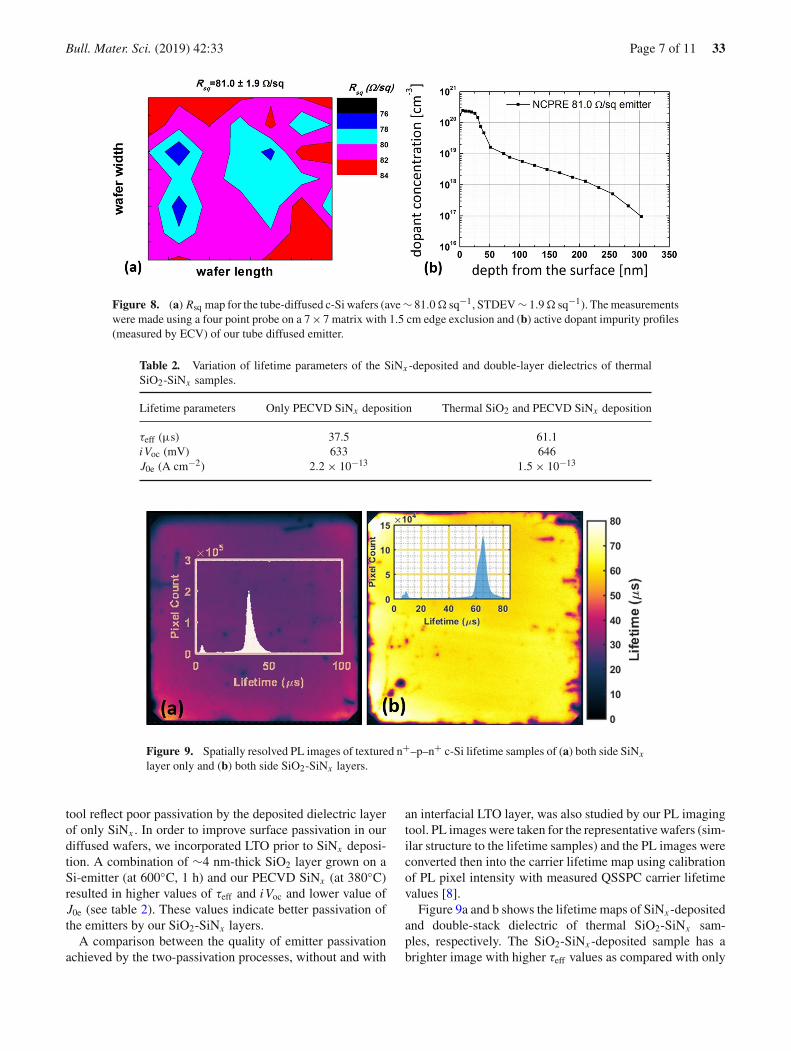
map and is shown in figure 8a.The average (ave) Rsq value of 81 � sq−1 with a STDEV
of 1.9 � sq−1 (measured over 49 points) for the P-diffusedemitter in the NCPRE diffusion furnace shows formation ofan excellent emitter for our cell. The distribution of P dopantsduring our P diffusion process is studied by ECV and thedopant profile is shown in figure 8b. The peak dopant con-centration is ∼2.4 × 1020 cm−3 and the junction depth is∼0.30 µm. Here we have used a dopant concentration of1 × 1017 cm−3 as an approximate value of the end of theemitter junction for all the diffused wafers as a reference forthe calculation of the junction depth [7].
3.1c Surface passivation: The conventional process of sur-face passivation of P-doped c-Si wafers is by the depositionof SiNx in the PECVD process [5]. This layer must providean emitter surface passivation and simultaneously also act as
33 Page 6 of 11 Bull. Mater. Sci. (2019) 42:33
Figure 6. Photos of the diffusion exhaust port at different scenarios: (a) the exhaust outlet port (viewed from insideafter unloading the loader) originally present. The inset shows the amount of gap left for suction (circled) by the exhaust.(b) Our designed quartz plate with five holes (1 cm diameter each). (c) The modified exhaust outlet port (viewed frominside after unloading the loader) after placing the additional quartz plate. The inset shows the reduced amount of gap leftfor suction (circled) by the exhaust. (d) The side view of the modified exhaust port. No visible gap is observed betweenthe two quartz plates.
Figure 7. The diffusion recipe of our two-step diffusion process.The table in the inset shows gas flows during respective steps indiffusion.
an ARC layer. Our PECVD SiNx deposition was performedfor 3 min at the substrate temperature of 380◦C. During theprocess, silane, ammonia and carrier gas flows were 25, 20and 980 sccm, respectively, for 390 s (RF power of 20 W andchamber pressure of 650 mTorr). The passivation propertieswere analysed by the values of the lifetime parameters, i.e.,τeff , implied open circuit voltage (iVoc) and emitter reversesaturation current density (J0e). The lifetime parameter valueswere measured using the Sinton tool after dielectric deposi-tions and are shown in table 2.
After PECVD SiNx deposition in our tool, the values of τeff
and iVoc are quite low. The reason behind this in our PECVDtool is that it is limited by the maximum achievable substratetemperature of 380◦C. However, the conventional process forpassivation of the P-diffused emitter on the c-Si surface isby the deposition of SiNx of proper thickness and refractiveindex at 450◦C [2]. These low values of τeff and iVoc in our
Bull. Mater. Sci. (2019) 42:33 Page 7 of 11 33
Figure 8. (a) Rsq map for the tube-diffused c-Si wafers (ave ∼ 81.0 � sq−1, STDEV ∼ 1.9 � sq−1). The measurementswere made using a four point probe on a 7 × 7 matrix with 1.5 cm edge exclusion and (b) active dopant impurity profiles(measured by ECV) of our tube diffused emitter.
Table 2. Variation of lifetime parameters of the SiNx -deposited and double-layer dielectrics of thermalSiO2-SiNx samples.
Lifetime parameters Only PECVD SiNx deposition Thermal SiO2 and PECVD SiNx deposition
τeff (µs) 37.5 61.1iVoc (mV) 633 646J0e (A cm−2) 2.2 × 10⁻¹³ 1.5 × 10⁻¹³
Figure 9. Spatially resolved PL images of textured n+–p–n+ c-Si lifetime samples of (a) both side SiNx
layer only and (b) both side SiO2-SiNx layers.
tool reflect poor passivation by the deposited dielectric layerof only SiNx . In order to improve surface passivation in ourdiffused wafers, we incorporated LTO prior to SiNx deposi-tion. A combination of ∼4 nm-thick SiO2 layer grown on aSi-emitter (at 600◦C, 1 h) and our PECVD SiNx (at 380◦C)resulted in higher values of τeff and iVoc and lower value ofJ0e (see table 2). These values indicate better passivation ofthe emitters by our SiO2-SiNx layers.
A comparison between the quality of emitter passivationachieved by the two-passivation processes, without and with
an interfacial LTO layer, was also studied by our PL imagingtool. PL images were taken for the representative wafers (sim-ilar structure to the lifetime samples) and the PL images wereconverted then into the carrier lifetime map using calibrationof PL pixel intensity with measured QSSPC carrier lifetimevalues [8].
Figure 9a and b shows the lifetime maps of SiNx -depositedand double-stack dielectric of thermal SiO2-SiNx sam-ples, respectively. The SiO2-SiNx -deposited sample has abrighter image with higher τeff values as compared with only
33 Page 8 of 11 Bull. Mater. Sci. (2019) 42:33
Figure 10. Photos of the printed cells: (a) front Ag-printed position of cell along the cell edge and(b) rear Al-printed position of cell along the cell edge. In both the cases, ∼2 mm width of Si remainsnon-metallized.
SiNx -deposited one. Besides, both the images are veryuniform in their distribution of τeff values all over the waferareas. This reflects the uniformity and effectiveness of ournovel passivation process even with the limitations of low-plasma temperature of 380◦C. The insets of figure 9a and bshow the distribution of τeff values throughout the entire wafersurfaces and these indicates a narrower distribution of τeff inboth the cases with only SiNx and double-stack SiO2-SiNx
dielectric-deposited samples.After final ARC deposition of SiNx , the surface reflectance
variation on the representative textured (also diffused andoxidized) c-Si wafer is shown in figure 5. These spectralreflectance values for the ARC wafers with low value of WAR(∼2.3%) confirm excellent optical properties for our dielec-tric deposition process.
3.1d Junction isolation: Effective removal of a parasiticjunction from the edge is critical to decrease the influenceof shunt resistance (Rsh). At present, complete rear junctionremoval in an acidic solution [9] is the standard industrial pro-cess. However, these acid-based inline rear junction isolationtools are non-affordable in a low-cost and small-footprint lablike ours. The alternate option thus chosen in our case is aplasma-edge isolation tool using sulphur hexafluoride (SF6)gas. Our process can effectively etch a P-doped Si layer alongthe edges of the diffused wafer with an approximate etch widthof <1 mm. High values of Rsh (>15 k� cm2) measured fromthe dark I–V characteristics of our cells further confirm ouroptimized edge isolation process.
3.1e Metallization: Screen printed contacts were used forfront Ag and back Al metallization of our cells. The frontscreen has been designed using Griddler simulation [10] fora proper conducting Ag-paste. However, our low-cost screenprinter has several limitations. It cannot print < 60 µm fin-ger width, squeeze pressure is not uniform over the whole6 inch pseudo-square wafer surface during printing andthe wafer alignment process is completely manual. Underthese limitations, printing is restricted to using front screen
Figure 11. The RTP firing profile used with a peak temperature of770◦C.
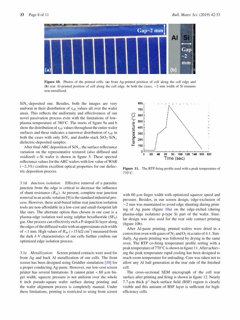
with 60 µm finger width with optimized squeeze speed andpressure. Besides, in our screen design, edge-exclusion of∼2 mm was maintained to avoid edge shunting during print-ing of Ag paste (figure 10a) on the edge-etched (duringplasma-edge isolation) p-type Si part of the wafer. Simi-lar design was also used for the rear side contact printing(figure 10b).
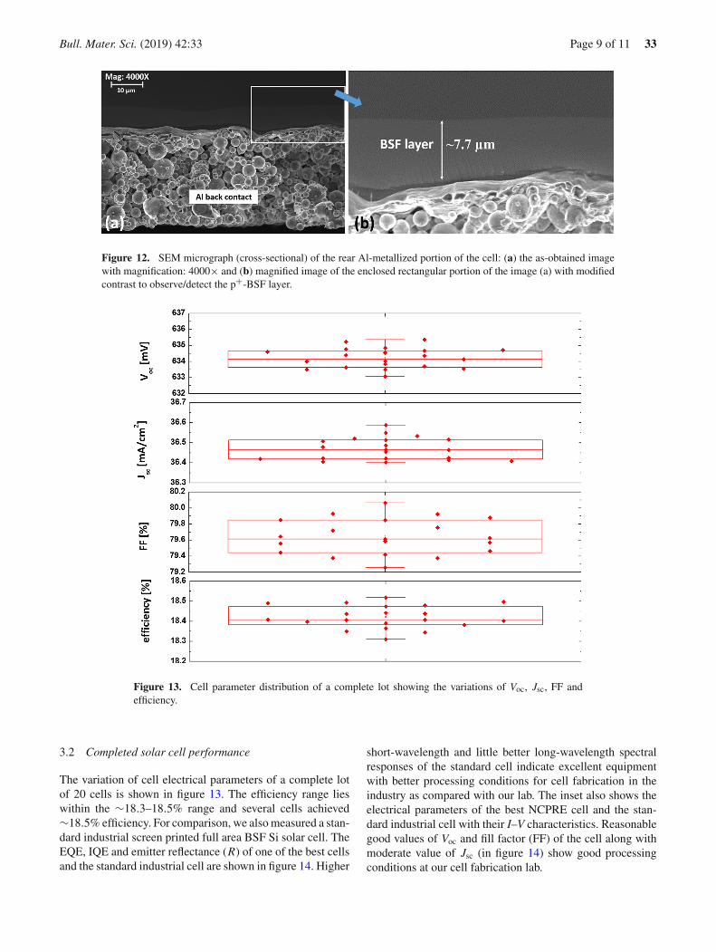
After Al-paste printing, printed wafers were dried in aconvection oven with gases of N2 and O2 in a ratio of 4:1. Sim-ilarly, Ag-paste printing was followed by drying in the sameoven. The RTP co-firing temperature profile setting with apeak temperature of 770◦C is shown in figure 11. After achiev-ing the peak temperature rapid cooling has been designed toreach room temperature for unloading. Care was taken not toallow any Al ball generation at the rear side of the finishedcell.
The cross-sectional SEM micrograph of the cell rearsurface after printing and firing is shown in figure 12. Nearly7.7µm thick p+-back-surface field (BSF) region is clearlyvisible and this amount of BSF layer is sufficient for high-efficiency cells.
Bull. Mater. Sci. (2019) 42:33 Page 9 of 11 33
Figure 12. SEM micrograph (cross-sectional) of the rear Al-metallized portion of the cell: (a) the as-obtained imagewith magnification: 4000× and (b) magnified image of the enclosed rectangular portion of the image (a) with modifiedcontrast to observe/detect the p+-BSF layer.
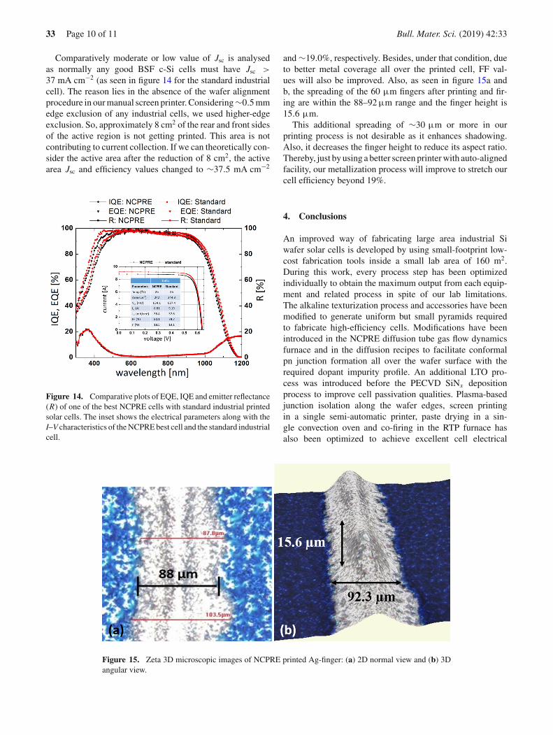
Figure 13. Cell parameter distribution of a complete lot showing the variations of Voc, Jsc, FF andefficiency.
3.2 Completed solar cell performance
The variation of cell electrical parameters of a complete lotof 20 cells is shown in figure 13. The efficiency range lieswithin the ∼18.3–18.5% range and several cells achieved∼18.5% efficiency. For comparison, we also measured a stan-dard industrial screen printed full area BSF Si solar cell. TheEQE, IQE and emitter reflectance (R) of one of the best cellsand the standard industrial cell are shown in figure 14. Higher
short-wavelength and little better long-wavelength spectralresponses of the standard cell indicate excellent equipmentwith better processing conditions for cell fabrication in theindustry as compared with our lab. The inset also shows theelectrical parameters of the best NCPRE cell and the stan-dard industrial cell with their I–V characteristics. Reasonablegood values of Voc and fill factor (FF) of the cell along withmoderate value of Jsc (in figure 14) show good processingconditions at our cell fabrication lab.
33 Page 10 of 11 Bull. Mater. Sci. (2019) 42:33
Comparatively moderate or low value of Jsc is analysedas normally any good BSF c-Si cells must have Jsc >
37 mA cm−2 (as seen in figure 14 for the standard industrialcell). The reason lies in the absence of the wafer alignmentprocedure in our manual screen printer. Considering ∼0.5 mmedge exclusion of any industrial cells, we used higher-edgeexclusion. So, approximately 8 cm2 of the rear and front sidesof the active region is not getting printed. This area is notcontributing to current collection. If we can theoretically con-sider the active area after the reduction of 8 cm2, the activearea Jsc and efficiency values changed to ∼37.5 mA cm−2
Figure 14. Comparative plots of EQE, IQE and emitter reflectance(R) of one of the best NCPRE cells with standard industrial printedsolar cells. The inset shows the electrical parameters along with theI–V characteristics of the NCPRE best cell and the standard industrialcell.
and ∼19.0%, respectively. Besides, under that condition, dueto better metal coverage all over the printed cell, FF val-ues will also be improved. Also, as seen in figure 15a andb, the spreading of the 60 µm fingers after printing and fir-ing are within the 88–92µm range and the finger height is15.6 µm.
This additional spreading of ∼30 µm or more in ourprinting process is not desirable as it enhances shadowing.Also, it decreases the finger height to reduce its aspect ratio.Thereby, just by using a better screen printer with auto-alignedfacility, our metallization process will improve to stretch ourcell efficiency beyond 19%.
4. Conclusions
An improved way of fabricating large area industrial Siwafer solar cells is developed by using small-footprint low-cost fabrication tools inside a small lab area of 160 m2.During this work, every process step has been optimizedindividually to obtain the maximum output from each equip-ment and related process in spite of our lab limitations.The alkaline texturization process and accessories have beenmodified to generate uniform but small pyramids requiredto fabricate high-efficiency cells. Modifications have beenintroduced in the NCPRE diffusion tube gas flow dynamicsfurnace and in the diffusion recipes to facilitate conformalpn junction formation all over the wafer surface with therequired dopant impurity profile. An additional LTO pro-cess was introduced before the PECVD SiNx depositionprocess to improve cell passivation qualities. Plasma-basedjunction isolation along the wafer edges, screen printingin a single semi-automatic printer, paste drying in a sin-gle convection oven and co-firing in the RTP furnace hasalso been optimized to achieve excellent cell electrical
Figure 15. Zeta 3D microscopic images of NCPRE printed Ag-finger: (a) 2D normal view and (b) 3Dangular view.
Bull. Mater. Sci. (2019) 42:33 Page 11 of 11 33
parameters. All the above developments finally led us tofabricate 6 inch pseudo-square DWS Cz industrial Si solarcells of actual and active area efficiencies of 18.5 and 19%(under AM1.5G 1 Sun) reproducibly and consistently atour lab. Our study suggests the possibility of fabricatinghigh-efficiency c-Si industrial cells successfully even in anysmall lab with low-cost lab equipment by taking care ofeach processing step scientifically with necessary correctivemeasures.
Acknowledgements
We would like to acknowledge the efforts of Nimisha S,Aditya D, Divya P and other colleagues at NCPRE for theirassistance in characterization and processing. This work wascarried out at the National Centre for Photovoltaic Researchand Education (funded by the Ministry of New and Renew-able Energy, Government of India) under the project no.16MNRE002 at IIT Bombay.
References
[1] ITRPV 2017 Eighth edition www.itrpv.net/Reports/Downloads/
[2] Basu P, Hameiri Z, Sarangi D, Cunnusamy J, Carmona E andBoreland M 2013 Sol. Energy Mater. Sol. Cells 117 412
[3] Basu P, Sarangi D, Shetty K and Boreland M 2013 Sol. EnergyMater. Sol. Cells 113 37
[4] Dastgheib-Shirazi A, Haverkamp H, Raabe B, Book F andHahn G 2008Proc. of 23rdEuropean photovoltaic solar energyconference, p 1197
[5] Duttagupta S, Lin F, Shetty K, Aberle A and Hoex B 2013Prog. Phot.: Res. Appl. 21 760
[6] Basu P, Sreejith K, Yadav T, Kottantharayil A and Sharma A2018 Sol. Energy Mat. Sol. Cells 185 406
[7] Hoornstra J, Van Strien W, Lamers M, Tool K and Weeber A2007 Proc. of 22nd European photovoltaic solar energy con-ference, p 1586
[8] Giesecke J, Schubert M, Michl B, Schindler F and Warta W2011 Sol. Energy Mater. Sol. Cells 95 1011
[9] Basu P, Law F, Vinodh S, Kumar A, Richter P, Bottari F et al2015 Sol. Energy Mater. Sol. Cells 137 193
[10] Wong J 2013 Proc. of 39th IEEE photovoltaic specialists con-ference p 933