Embed Size (px)
Citation preview

Characterization of free-standing InAs quantum membranes by standing wave hardx-ray photoemission spectroscopyG. Conti, S. Nemšák, C.-T. Kuo, M. Gehlmann, C. Conlon, A. Keqi, A. Rattanachata, O. Karslıoğlu, J. Mueller,J. Sethian, H. Bluhm, J. E. Rault, J. P. Rueff, H. Fang, A. Javey, and C. S. Fadley
Citation: APL Materials 6, 058101 (2018); doi: 10.1063/1.5022379View online: https://doi.org/10.1063/1.5022379View Table of Contents: http://aip.scitation.org/toc/apm/6/5Published by the American Institute of Physics
Articles you may be interested inMinimizing performance degradation induced by interfacial recombination in perovskite solar cells throughtailoring of the transport layer electronic propertiesAPL Materials 6, 036104 (2018); 10.1063/1.5021138
Single crystalline electronic structure and growth mechanism of aligned square graphene sheetsAPL Materials 6, 036107 (2018); 10.1063/1.5012947
Structural analysis of LaVO3 thin films under epitaxial strainAPL Materials 6, 046102 (2018); 10.1063/1.5021844
Synthesis science of SrRuO3 and CaRuO3 epitaxial films with high residual resistivity ratiosAPL Materials 6, 046101 (2018); 10.1063/1.5023477
Improving the thermoelectric performance in Mg3+xSb1.5Bi0.49Te0.01 by reducing excess MgAPL Materials 6, 016106 (2018); 10.1063/1.5011379
Thickness dependence of the quantum Hall effect in films of the three-dimensional Dirac semimetal Cd3As2APL Materials 6, 026105 (2018); 10.1063/1.5016866
APL MATERIALS 6, 058101 (2018)
Characterization of free-standing InAs quantummembranes by standing wave hard x-rayphotoemission spectroscopy
G. Conti,1,2 S. Nemsak,1,2,3,4 C.-T. Kuo,1,2 M. Gehlmann,1,2,3 C. Conlon,1,2
A. Keqi,1,2 A. Rattanachata,1,2 O. Karslıoglu,5 J. Mueller,6 J. Sethian,7
H. Bluhm,4,5 J. E. Rault,8 J. P. Rueff,8,9 H. Fang,10 A. Javey,2,11
and C. S. Fadley1,21Department of Physics, University of California Davis, Davis, California 95616, USA2Materials Sciences Division, Lawrence Berkeley National Laboratory, Berkeley,California 94720, USA3Peter-Grunberg-Institut PGI-6, Forschungszentrum Julich, 52425 Julich, Germany4Advanced Light Source, Lawrence Berkeley National Laboratory, Berkeley,California 94720, USA5Chemical Sciences Division, Lawrence Berkeley National Laboratory, Berkeley,California 94720, USA6Center for Computational Sciences and Engineering, Lawrence Berkeley National Laboratory,Berkeley, California 94720, USA7Department of Mathematics, University of California Berkeley, Berkeley,California 94720, USA8Synchrotron-SOLEIL, BP 48, Saint-Aubin, F91192 Gif sur Yvette Cedex, France9Laboratoire de Chimie Physique–Matiere et Rayonnement, UPMC Universite Paris 06, CNRS,UMR 7614, Sorbonne Universite, 75005 Paris Cedex 05, France10Department of Electrical and Computer Engineering, Northeastern University, Boston,Massachusetts 02115, USA11Electrical Engineering and Computer Sciences, University of California Berkeley, Berkeley,California 94720, USA
(Received 14 January 2018; accepted 7 March 2018; published online 6 April 2018)
Free-standing nanoribbons of InAs quantum membranes (QMs) transferred onto a(Si/Mo) multilayer mirror substrate are characterized by hard x-ray photoemissionspectroscopy (HXPS) and by standing-wave HXPS (SW-HXPS). Information on thechemical composition and on the chemical states of the elements within the nanorib-bons was obtained by HXPS and on the quantitative depth profiles by SW-HXPS. Bycomparing the experimental SW-HXPS rocking curves to x-ray optical calculations,the chemical depth profile of the InAs(QM) and its interfaces were quantitativelyderived with angstrom precision. We determined that (i) the exposure to air inducedthe formation of an InAsO4 layer on top of the stoichiometric InAs(QM); (ii) thetop interface between the air-side InAsO4 and the InAs(QM) is not sharp, indicat-ing that interdiffusion occurs between these two layers; (iii) the bottom interfacebetween the InAs(QM) and the native oxide SiO2 on top of the (Si/Mo) substrateis abrupt. In addition, the valence band offset (VBO) between the InAs(QM) and theSiO2/(Si/Mo) substrate was determined by HXPS. The value of VBO = 0.2± 0.04 eV isin good agreement with literature results obtained by electrical characterization, givinga clear indication of the formation of a well-defined and abrupt InAs/SiO2 heterojunc-tion. We have demonstrated that HXPS and SW-HXPS are non-destructive, powerfulmethods for characterizing interfaces and for providing chemical depth profiles ofnanostructures, quantum membranes, and 2D layered materials. © 2018 Author(s).All article content, except where otherwise noted, is licensed under a CreativeCommons Attribution (CC BY) license (http://creativecommons.org/licenses/by/4.0/).https://doi.org/10.1063/1.5022379
III-V compound semiconductors possess superior carrier transport and excellent optoelectronicproperties, which render them widely used in high performance electronic and optoelectronic devices,
2166-532X/2018/6(5)/058101/8 6, 058101-1 © Author(s) 2018
058101-2 Conti et al. APL Mater. 6, 058101 (2018)
such as high electron mobility transistors, heterostructure lasers, and solar cells.1–3 These III-V “alter-native” semiconductors, such as InAs and InGaSb, have much higher electron/hole mobility than Siand are good candidates to replace Si as future channel materials in metal–oxide–semiconductorfield-effect transistors (MOSFETs).4–7 However, the growth of these semiconductors and their inte-gration with the low-cost processing of Si technology present challenges since high defect densitiesand junction leakage currents may occur at the interface between these compounds and the Sisubstrate8 due to their lattice mismatch. In order to overcome the problems related to the growthof these semiconductors on Si or SiO2 substrates and to their integration with the more matureSi-based processes, Javey et al.9 developed a method for transferring ultrathin free-standing crys-talline III-Vs films on a user-defined substrate. This transfer step led to high-performance III-Vcomplementary metal–oxide–semiconductor (CMOS) and radio frequency (RF) circuits on both Siand plastic substrates.10 However, the non-destructive characterization of these transferred films is stilla challenge. In particular, their depth-resolved chemical composition and the intermixing/oxidationoccurring at the interfaces have not been fully determined. Low- and high-resolution transmissionelectron microscopy (TEM) characterization on such membranes has been performed by Javey etal.11 However, it is well known that the sample preparation for TEM analysis can induce damagesto the material and can create interdiffusion at the interfaces.12 Therefore, TEM has limitationsas a technique for a non-destructive, quantitative characterization of the interfaces of quantummembranes. On the other hand, the characterization of these interfaces is fundamental for highperformance nanoscale transistors. It is known that oxide layers on the surface,13 or at the inter-face, strongly influence the electronic transport properties of these materials, especially in the caseof nanowires and quantum membranes. For instance, the native oxide layer could shift the positionof the surface Fermi-level or even induce Fermi-level pinning, which significantly degrades deviceperformances.11,14,15
In this paper, we show that hard x-ray photoemission spectroscopy (HXPS) and standing waveHXPS (SW-HXPS) can be used to characterize bulks and buried layers/buried interfaces withoutaltering the samples. Standard XPS analysis provides information on the chemical and electronicstates of each element at the surface. Moving to hard x-ray photon energies (2–15 keV), and thus tolarger electron inelastic mean-free paths (IMFPs),16 allows one to obtain information on chemicaland electronic states of the bulk and of the buried interfaces.17 Among the many III-V alternativesemiconductors, we chose to study free-standing InAs quantum membranes [InAs(QM)] which, inaddition to their interesting properties, represent a more general class of 2-D materials. For instance,it has been reported9,11 that when the thickness of InAs is reduced, especially when it is belowits exciton Bohr radius (34 nm), strong quantum confinement effects start to emerge and its bandstructure can be precisely tuned from bulk to 2D by changing the thickness. In particular, we havestudied by SW-HXPS the possible formation of a surface oxide layer and interdiffusion at the topand bottom interfaces of InAs(QM) nanoribbons. Furthermore, we have determined if and what kindof oxide layer is formed at the top vacuum/InAs interface and how abrupt the InAs/bottom layerinterface is.
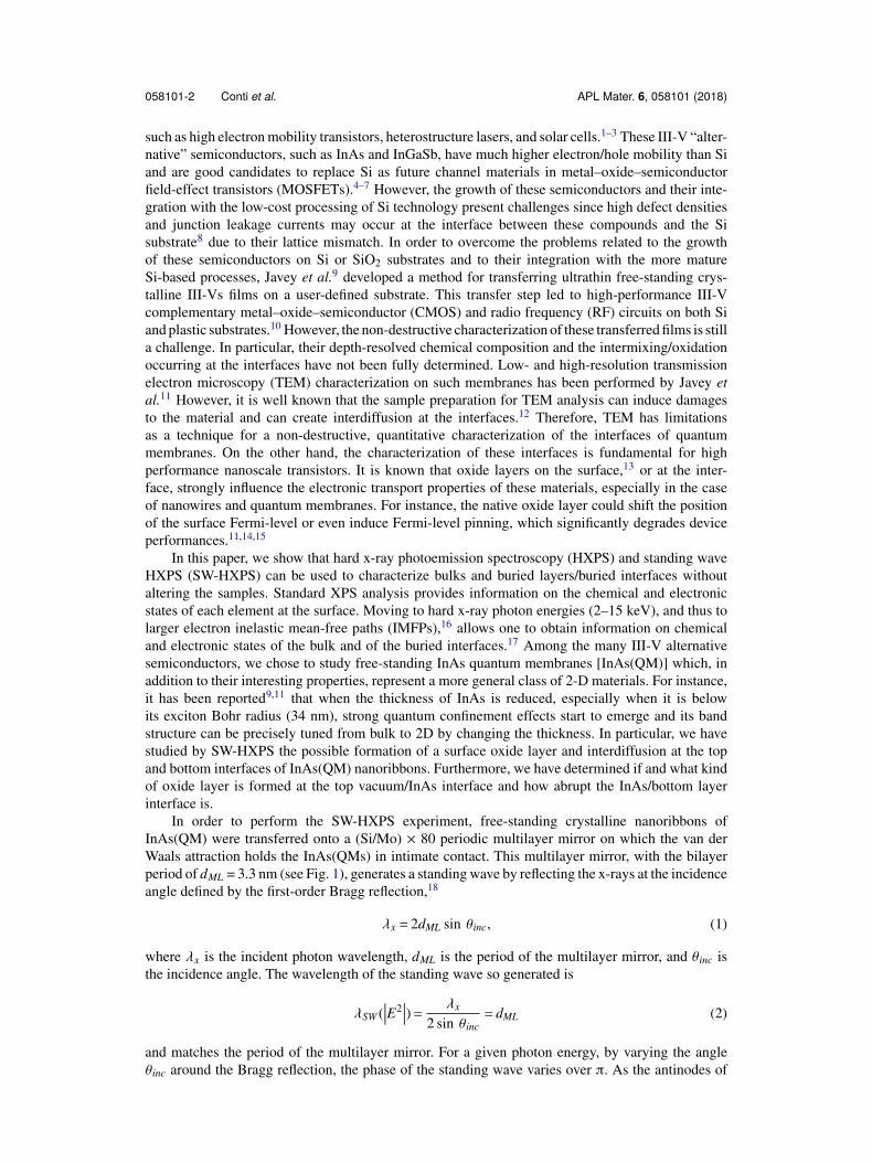
In order to perform the SW-HXPS experiment, free-standing crystalline nanoribbons ofInAs(QM) were transferred onto a (Si/Mo) × 80 periodic multilayer mirror on which the van derWaals attraction holds the InAs(QMs) in intimate contact. This multilayer mirror, with the bilayerperiod of dML = 3.3 nm (see Fig. 1), generates a standing wave by reflecting the x-rays at the incidenceangle defined by the first-order Bragg reflection,18
λx = 2dML sin θinc, (1)
where λx is the incident photon wavelength, dML is the period of the multilayer mirror, and θinc isthe incidence angle. The wavelength of the standing wave so generated is
λSW (���E2���)=
λx
2 sin θinc= dML (2)
and matches the period of the multilayer mirror. For a given photon energy, by varying the angleθinc around the Bragg reflection, the phase of the standing wave varies over π. As the antinodes of
058101-3 Conti et al. APL Mater. 6, 058101 (2018)
FIG. 1. Schematic of the InAs(QM) nanoribbons transferred onto a (Si/Mo) × 80 multilayer (dimensions not to scale) onwhich the van der Waals attraction holds the InAs(QMs) in intimate contact. Each nanoribbon is 15 nm thick and 300 nmwide, and the distance between one ribbon and its neighbors is 300 nm. The multilayer period is 3.3 nm.
the electromagnetic field shift vertically through the sample, they highlight different depths in thesample. This provides depth selectivity to the photoemission process. In our case, the standing wave,which travels perpendicularly to the multilayer and to the sample surfaces deposited on it, allows usto obtain a quantitative chemical depth profile of the InAs(QM) and of its interfaces with vacuumand with the SiO2/mirror substrate. The vertical resolution is approximately 1/10 of the SW period,which is ≈0.3 nm for the mirror used in this study.19,20
The InAs(QM) in the shape of nanoribbons was epitaxially grown on the GaSb/AlGaSb substratealong the [111] plane.9 Each nanoribbon is 15 nm thick and 300 nm wide, and the distance betweenone ribbon and its neighbors is 300 nm (Fig. 1). The (Si/Mo) multilayer onto which these InAs(QM)nanoribbons were transferred was prepared at the Center for X-ray Optics of the Lawrence BerkeleyNational Laboratory and consists of 80 (Si/Mo) bilayers, each bilayer having a thickness of 3.3 nm.The termination layer of this (Si/Mo) mirror was chosen to be Si, which, exposed to air, gives rise toa thin layer of native silicon oxide (SiO2). In this way, the bottom interface between the InAs(QM)and the SiO2/(Si/Mo) substrate is a good approximation to the interface between the InAs(QM) anda typical silicon-based substrate. Before transferring the InAs(QM) on it, the mirror was cleanedwith acetone, isopropyl alcohol, and de-ionized water.9 At the photon energy of 4.0 keV used in ourmeasurements, the Bragg angle is θBragg ≈ 2.7◦. In order to scan over the first order Bragg reflection,the incidence angle of the incoming x-ray beam was varied between 2.4◦ and 3.5◦, in steps 0.02◦. TheHXPS spectra were obtained at the Advanced Light Source (ALS) (Beamline 9.3.0) and at SOLEILSynchrotron (GALAXIES Beamline).21 The p-polarized x-ray photon energy was set to hν = 4.0 keV,and the spectral total energy resolution was ≈500 meV for the data acquired at ALS and ≈250 meVfor the data acquired at SOLEIL. At hν = 4.0 keV, the IMFP, as estimated from the TPP-2M formula,22
is ∼7 nm for InAs. As a consequence, not only the top surface but also the bottom interface betweenthe InAs(QM) and the SiO2(Si/Mo) substrate could be characterized by HXPS. The geometry of theexperiment is as follows: the angle between x-ray incidence and photoelectron exit is 90◦ and theincidence angle relative to the sample surface is 2.4◦-3.0◦. Thus, the photoelectron takeoff angle withrespect to the surface is from 87.6◦ to 87.0◦ and essentially along the surface normal. The bindingenergies of the HXPS spectra were calibrated using Au 4f and Au EF before and after each dataacquisition.
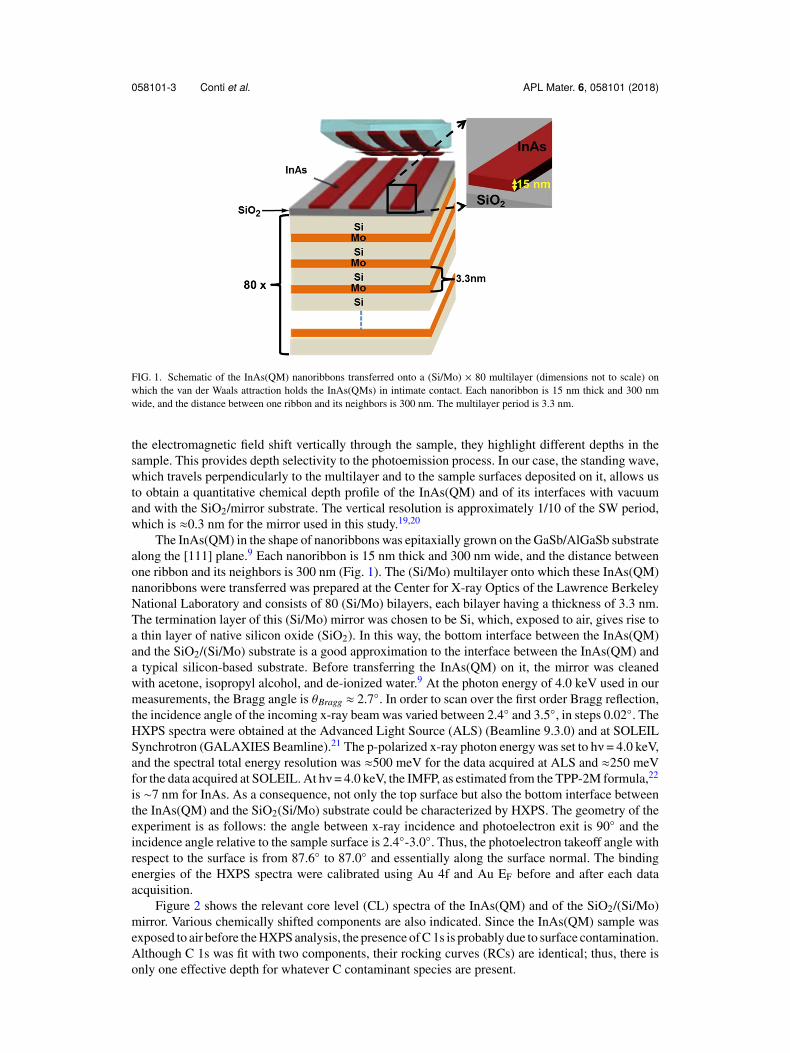
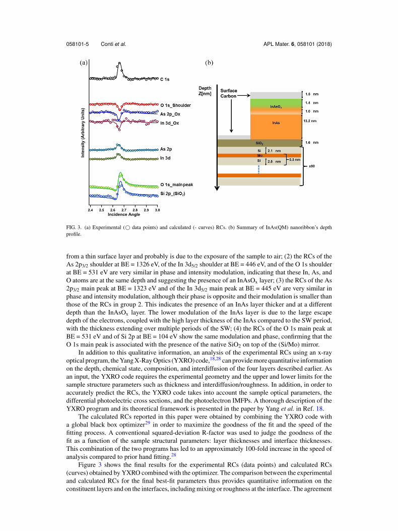
Figure 2 shows the relevant core level (CL) spectra of the InAs(QM) and of the SiO2/(Si/Mo)mirror. Various chemically shifted components are also indicated. Since the InAs(QM) sample wasexposed to air before the HXPS analysis, the presence of C 1s is probably due to surface contamination.Although C 1s was fit with two components, their rocking curves (RCs) are identical; thus, there isonly one effective depth for whatever C contaminant species are present.
058101-4 Conti et al. APL Mater. 6, 058101 (2018)
FIG. 2. Experimental x-ray photoelectron core level spectra for all of the elements in the InAs(QM) and the mirror substrate:C 1s, O 1s, As 2p3/2, In 3d5/2, Mo 3d, and Si 2p, with chemically shifted components indicated.
Each of the As 2p, In 3d, Si 2p, and O 1s CL spectra shows clear evidence of two components.As reported in the literature,23,24 the As 2p shoulder at binding energy (BE) = 1326 eV and that ofIn 3d at BE = 446 eV are attributed to the presence of AsOx and InOx, and the weak Si 2p peak atBE = 103.5 eV is assigned to the native SiO2 on top of the (Si/Mo) mirror. The depth distribution ofthese elements and of their different valence states can be obtained by SW-HXPS, including the twoO 1s components, the main peak at BE = 533.4 eV, and the shoulder at BE = 531 eV. The CL spectrawere analyzed by subtracting a Shirley background25–27 from each spectrum before fitting it withVoigt functions. The peak integrated intensity of each CL was then plotted versus the incidence angle,thus generating what we call experimental rocking curves (RCs). The RCs so obtained are shownin Fig. 3(a) (data points). From these RCs, a qualitative picture of the chemical depth profile of theInAs(QM) nanoribbons can be obtained. All the RCs show a maximum or minimum at the incidenceangle ≈2.7◦ that corresponds to the Bragg peak of the (Si/Mo) multilayer. In addition, we observethat the RCs can be grouped into four different categories: (1) the RC of C 1s, including its strongmodulation, does not match with any other RCs. Its strong RC modulation suggests that C origins
058101-5 Conti et al. APL Mater. 6, 058101 (2018)
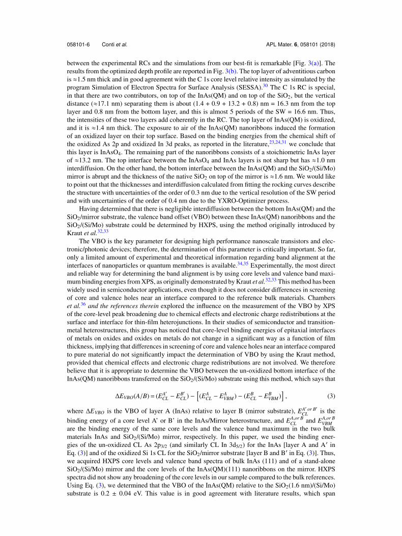
FIG. 3. (a) Experimental (© data points) and calculated (- curves) RCs. (b) Summary of InAs(QM) nanoribbon’s depthprofile.
from a thin surface layer and probably is due to the exposure of the sample to air; (2) the RCs of theAs 2p3/2 shoulder at BE = 1326 eV, of the In 3d5/2 shoulder at BE = 446 eV, and of the O 1s shoulderat BE = 531 eV are very similar in phase and intensity modulation, indicating that these In, As, andO atoms are at the same depth and suggesting the presence of an InAsOx layer; (3) the RCs of the As2p3/2 main peak at BE = 1323 eV and of the In 3d5/2 main peak at BE = 445 eV are very similar inphase and intensity modulation, although their phase is opposite and their modulation is smaller thanthose of the RCs in group 2. This indicates the presence of an InAs layer thicker and at a differentdepth than the InAsOx layer. The lower modulation of the InAs layer is due to the large escapedepth of the electrons, coupled with the high layer thickness of the InAs compared to the SW period,with the thickness extending over multiple periods of the SW; (4) the RCs of the O 1s main peak atBE = 531 eV and of Si 2p at BE = 104 eV show the same modulation and phase, confirming that theO 1s main peak is associated with the presence of the native SiO2 on top of the (Si/Mo) mirror.
In addition to this qualitative information, an analysis of the experimental RCs using an x-rayoptical program, the Yang X-Ray Optics (YXRO) code,18,28 can provide more quantitative informationon the depth, chemical state, composition, and interdiffusion of the four layers described earlier. Asan input, the YXRO code requires the experimental geometry and the upper and lower limits for thesample structure parameters such as thickness and interdiffusion/roughness. In addition, in order toaccurately predict the RCs, the YXRO code takes into account the sample optical parameters, thedifferential photoelectric cross sections, and the photoelectron IMFPs. A thorough description of theYXRO program and its theoretical framework is presented in the paper by Yang et al. in Ref. 18.
The calculated RCs reported in this paper were obtained by combining the YXRO code witha global black box optimizer29 in order to maximize the goodness of the fit and the speed of thefitting process. A conventional squared-deviation R-factor was used to judge the goodness of thefit as a function of the sample structural parameters: layer thicknesses and interface thicknesses.This combination of the two programs has led to an approximately 100-fold increase in the speed ofanalysis compared to prior hand fitting.28
Figure 3 shows the final results for the experimental RCs (data points) and calculated RCs(curves) obtained by YXRO combined with the optimizer. The comparison between the experimentaland calculated RCs for the final best-fit parameters thus provides quantitative information on theconstituent layers and on the interfaces, including mixing or roughness at the interface. The agreement
058101-6 Conti et al. APL Mater. 6, 058101 (2018)
between the experimental RCs and the simulations from our best-fit is remarkable [Fig. 3(a)]. Theresults from the optimized depth profile are reported in Fig. 3(b). The top layer of adventitious carbonis ≈1.5 nm thick and in good agreement with the C 1s core level relative intensity as simulated by theprogram Simulation of Electron Spectra for Surface Analysis (SESSA).30 The C 1s RC is special,in that there are two contributors, on top of the InAs(QM) and on top of the SiO2, but the verticaldistance (≈17.1 nm) separating them is about (1.4 + 0.9 + 13.2 + 0.8) nm = 16.3 nm from the toplayer and 0.8 nm from the bottom layer, and this is almost 5 periods of the SW = 16.6 nm. Thus,the intensities of these two layers add coherently in the RC. The top layer of InAs(QM) is oxidized,and it is ≈1.4 nm thick. The exposure to air of the InAs(QM) nanoribbons induced the formationof an oxidized layer on their top surface. Based on the binding energies from the chemical shift ofthe oxidized As 2p and oxidized In 3d peaks, as reported in the literature,23,24,31 we conclude thatthis layer is InAsO4. The remaining part of the nanoribbons consists of a stoichiometric InAs layerof ≈13.2 nm. The top interface between the InAsO4 and InAs layers is not sharp but has ≈1.0 nminterdiffusion. On the other hand, the bottom interface between the InAs(QM) and the SiO2/(Si/Mo)mirror is abrupt and the thickness of the native SiO2 on top of the mirror is ≈1.6 nm. We would liketo point out that the thicknesses and interdiffusion calculated from fitting the rocking curves describethe structure with uncertainties of the order of 0.3 nm due to the vertical resolution of the SW periodand with uncertainties of the order of 0.4 nm due to the YXRO-Optimizer process.
Having determined that there is negligible interdiffusion between the bottom InAs(QM) and theSiO2/mirror substrate, the valence band offset (VBO) between these InAs(QM) nanoribbons and theSiO2/(Si/Mo) substrate could be determined by HXPS, using the method originally introduced byKraut et al.32,33
The VBO is the key parameter for designing high performance nanoscale transistors and elec-tronic/photonic devices; therefore, the determination of this parameter is critically important. So far,only a limited amount of experimental and theoretical information regarding band alignment at theinterfaces of nanoparticles or quantum membranes is available.34,35 Experimentally, the most directand reliable way for determining the band alignment is by using core levels and valence band maxi-mum binding energies from XPS, as originally demonstrated by Kraut et al.32,33 This method has beenwidely used in semiconductor applications, even though it does not consider differences in screeningof core and valence holes near an interface compared to the reference bulk materials. Chamberset al.36 and the references therein explored the influence on the measurement of the VBO by XPSof the core-level peak broadening due to chemical effects and electronic charge redistributions at thesurface and interface for thin-film heterojunctions. In their studies of semiconductor and transition-metal heterostructures, this group has noticed that core-level binding energies of epitaxial interfacesof metals on oxides and oxides on metals do not change in a significant way as a function of filmthickness, implying that differences in screening of core and valence holes near an interface comparedto pure material do not significantly impact the determination of VBO by using the Kraut method,provided that chemical effects and electronic charge redistributions are not involved. We thereforebelieve that it is appropriate to determine the VBO between the un-oxidized bottom interface of theInAs(QM) nanoribbons transferred on the SiO2/(Si/Mo) substrate using this method, which says that
∆EVBO(A/B)= (EA′CL − EB′
CL) −[(EA
CL − EAVBM ) − (EB
CL − EBVBM )
], (3)
where ∆EVBO is the VBO of layer A (InAs) relative to layer B (mirror substrate), EA′ or B′CL is the
binding energy of a core level A’ or B’ in the InAs/Mirror heterostructure, and EA,or BCL and EA,or B
VBMare the binding energy of the same core levels and the valence band maximum in the two bulkmaterials InAs and SiO2/(Si/Mo) mirror, respectively. In this paper, we used the binding ener-gies of the un-oxidized CL As 2p3/2 (and similarly CL In 3d5/2) for the InAs [layer A and A′ inEq. (3)] and of the oxidized Si 1s CL for the SiO2/mirror substrate [layer B and B′ in Eq. (3)]. Thus,we acquired HXPS core levels and valence band spectra of bulk InAs (111) and of a stand-aloneSiO2/(Si/Mo) mirror and the core levels of the InAs(QM)(111) nanoribbons on the mirror. HXPSspectra did not show any broadening of the core levels in our sample compared to the bulk references.Using Eq. (3), we determined that the VBO of the InAs(QM) relative to the SiO2(1.6 nm)/(Si/Mo)substrate is 0.2 ± 0.04 eV. This value is in good agreement with literature results, which span
058101-7 Conti et al. APL Mater. 6, 058101 (2018)
∼0.1-0.2 eV,37–40 as obtained by electrical characterization, especially considering the differencesbetween our InAs(QM)/SiO2 interface and the nanostructures previously studied in the literature.
In conclusion, we have demonstrated that HXPS and SW-HXPS are powerful non-destructivemethods that can be used to characterize the interfaces in novel materials and nanostructures such asquantum membranes. For instance, HXSP and SW-HXPS provided the stoichiometry, the depth, andthe thickness of the oxide overlayer on these InAs(QM) nanoribbons, which acts as passivation layer,useful in order to prevent dangling bonds. In addition, SW-HXPS showed that the interface betweenthe InAs(QM) and its oxidation layer is not sharp, indicating that some interdiffusion occurred and thatthe oxidation is not entirely homogenous. On the contrary, the bottom interface between the InAs(QM)and the substrate is atomically abrupt, which is a crucial prerequisite for successful applications ofhigh performance nanoscale transistors. In addition, the VBO between these InAs(QM) nanoribbonsand the SiO2/(Si/Mo) substrate was determined. The obtained value of 0.2 ± 0.04 eV is in goodagreement with literature results giving a clear indication of the formation of a well-defined andabrupt SiO2–InAs heterojunction.
This work was supported by the US Department of Energy under Contract No. DE-AC02-05CH11231 (Advanced Light Source, Materials Sciences and Chemical Sciences Divisions) and byDOE Contract No. DE-SC0014697 through the University of California Davis (salary for C.T.K.,M.G., and C.S.F.). C.S.F. has also been supported for salary by the Director, Office of Science,Office of Basic Energy Sciences (BSE), Materials Sciences and Engineering (MSE) Division, ofthe U.S. Department of Energy under Contract No. DE-AC02-05CH11231, through the LaboratoryDirected Research and Development Program of Lawrence Berkeley National Laboratory, through theAPTCOM Project, “Laboratoire d’Excellence Physics Atom Light Matter” (LabEx PALM) overseenby the French National Research Agency (ANR) as part of the “Investissements d’Avenir” program,and from the Julich Research Center, Peter Grunberg Institute, PGI-6. A.R. was funded by the RoyalThai Government, A.K. was awarded with graduate student researcher-work study and departmentalfellowship for at UC Davis, and C.C. was funded by GAANN program through UC Davis PhysicsDepartment. Materials processing was supported by the Electronic Materials Program funded by theDirector, Office of Science, Office of Basic Energy Sciences, Materials Sciences and EngineeringDivision of the U.S. Department of Energy, under Contract No. DE-AC02 05Ch11231. O.K. andH.B. acknowledge support by the Director, Office of Science, Office of Basic Energy Sciences (BSE),Chemicals Sciences, Geosciences and Biosciences, of the U.S. Department of Energy under ContractNo. DE-AC02 05CH1123.
1 M. Heyns and W. Tsai, MRS Bull. 34, 485 (2009).2 T.-W. Kim, D.-H. Kim, and J. A. Del Alamo, in IEEE International (IEEE, 2010), p. 496.3 T. J. Kempa, R. W. Day, S.-K. Kim, H.-G. Park, and C. M. Lieber, Energy Environ. Sci. 6, 719 (2013).4 S. Dhar, M. Pattanaik, and P. Rajaram, VLSI Des. 2011, 178516.5 T. Takahashi, K. Takei, E. Adabi, Z. Fan, A. M. Niknejad, and A. Javey, ACS Nano 4, 5855 (2010).6 K. Tomioka, M. Yoshimura, and T. A. Fukui, Nature 488, 189 (2012).7 M. Borg, H. Schmid, K. E. Moselund, G. Signorello, L. Gignac, J. Bruley, C. Breslin, P. Das Kanungo, P. Werner, and
H. Riel, Nano Lett. 14, 1914 (2014).8 S. M. Sze and J. C. Irvin, Solid-State Electron. 11, 599 (1968).9 H. Ko, K. Takei, R. Kapadia, S. H. Chuang, P. W. Leu, K. Ganapathi, E. Plis, H. S. Kim, S.-Y. Chen, M. Madsen, A. C. Ford,
Y.-L. Chueh, S. Krishna, S. Salahuddin, and A. Javey, Nature 468, 286 (2010).10 J. Nah, H. Fang, C. Wang, K. Takei, M. Hyung Lee, E. Plis, S. Krishna, and A. Javey, Nano Lett. 12, 3592 (2012).11 K. Takei, H. Fang, S. B. Kumar, R. Kapadia, Q. Gao, M. Madsen, H. S. Kim, C.-H. Liu, Y.-L. Chueh, E. Plis, S. Krishna,
H. A. Bechtel, J. Guo, and A. Javey, Nano Lett. 11, 5008 (2011).12 J. Mayer, L. A. Giannuzzi, T. Kamino, and J. Michael, MRS Bull. 32, 400 (2007).13 Q. Hang, F. Wang, P. D. Carpenter, D. Zemlyanov, D. Zakharov, E. A. Stach, W. E. Buhro, and D. B. Janes, Nano Lett. 8,
49 (2008).14 V. N. Brudnyia, S. N. Grinyaev, and N. G. Kolin, Phys. B 348, 213 (2004).15 E. Halpern, G. Elias, A. V. Kretinin, H. Shtrikman, and Y. Rosenwaks, Appl. Phys. Lett. 100, 262105 (2012).16 C. S. Fadley, C. J. Powell, and S. Tanuma, in Hard X-ray Angle-Resolved Photoelectron Spectroscopy (HARPES), edited
by J. Woicik (Springer, 2016), Chaps. 1 and 5.17 See fadley.physics.ucdavis.edu for Fadley Group Website.18 S.-H. Yang, A. X. Gray, A. M. Kaiser, B. S. Mun, B. C. Sell, J. B. Kortright, and C. S. Fadley, J. Appl. Phys. 113, 073513
(2013).19 F. Kronast, R. Ovsyannikov, A. Kaiser, C. Wiemann, S.-H. Yang, D. E. Burgler, R. Schreiber, F. Salmassi, P. Fischer,
H. A. Durr, C. M. Schneider, W. Eberhardt, and C. S. Fadley, Appl. Phys. Lett. 93, 243116 (2008).
058101-8 Conti et al. APL Mater. 6, 058101 (2018)
20 A. X. Gray, C. Papp, B. Balke, S.-H. Yang, M. Huijben, E. Rotenberg, A. Bostwick, S. Ueda, Y. Yamashita, K. Kobayashi,E. M. Gullikson, J. B. Kortright, F. M. F. de Groot, G. Rijnders, D. H. A. Blank, R. Ramesh, and C. S. Fadley, Phys. Rev.B 82, 205116 (2010).
21 J.-P. Rueff, J. M. Ablett, D. Ceolin, D. Prieur, Th. Moreno, V. Baledent, B. Lassalle, J. E. Rault, M. Simon, and A. Shukla,J. Synchrotron Radiat. 22, 175 (2015).
22 S. Tanuma, C. J. Powell, and D. R. Penn, Surf. Interface Anal. 43, 689 (2011).23 G. Hollinger, R. Skheyta-Kabbani, and M. Gendry, Phys. Rev. B 49, 11159 (1994).24 D. H. van Dorp, S. Arnauts, D. Cuypers, J. Rip, F. Holsteyns, and S. De Gendt, Solid State Phenom. 219, 56 (2015).25 D. A. Shirley, Phys. Rev. B 5, 4709 (1972).26 S. Tougaard, Appl. Surf. Sci. 100, 1 (1996).27 J. E. Castle and A. M. Salvi, J. Vac. Sci. Technol., A 19, 1170 (2001).28 See https://sites.google.com/a/lbl.gov/yxro for the YXRO open-access code, examples and references.29 M. Gehlmann, O. Karslıoglu, J. Mueller et al., YXRO and Optimizer, private communication (2017).30 W. Smekal, W. S. M. Werner, and C. J. Powell, Surf. Interface Anal. 37, 1059 (2005).31 R. Timm, A. Fian, M. Hjort, C. Thelander, E. Lind, J. N. Andersen, L.-E. Wernersson, and A. Mikkelsen, Appl. Phys. Lett.
97, 132904 (2010).32 E. A. Kraut, R. W. Grant, J. R. Waldrop, and S. P. Kowalczyk, Phys. Rev. Lett. 44, 1620 (1980).33 E. A. Kraut, R. W. Grant, J. R. Waldrop, and S. P. Kowalczyk, Phys. Rev. B 28, 1965 (1983).34 A. Franciosi and C. G. Van de Walle, Surf. Sci. Rep. 25, 1 (1996).35 M.-H. Chiu, C. Zhang, H.-W. Shiu, C.-P. Chuu, C.-H. Chen, C.-Y. S. Chang, C.-H. Chen, M.-Y. Chou, C.-K. Shih, and
L.-J. Li, Nat. Commun. 6, 7666 (2015).36 S. A. Chambers, Y. Du, R. B. Comes, S. R. Spurgeon, and P. V. Sushko, Appl. Phys. Lett. 110, 082104 (2017).37 A. Brenneis, J. Overbeck, J. Treu, S. Hertenberger, S. Morkotter, M. Doblinger, J. J. Finley, G. Abstreiter, G. Koblmuller,
and A. W. Holleitner, ACS Nano 9, 9849 (2015).38 M. T. Bjork, H. Schmid, C. D. Bessire, K. E. Moselund, H. Ghoneim, S. Karg, E. Lortscher, and H. Riel, Appl. Phys. Lett.
97, 163501 (2010).39 W. Wei, X.-Y. Bao, C. Soci, Y. Ding, Z.-L. Wang, and D. Wang, Nano Lett. 9, 2926 (2009).40 A. D. Mallorquı, E. Alarcon-Llado, E. Russo-Averchi, G. Tutuncuoglu, F. Matteini, D. Ruffer, and A. Fontcuberta i Morral,
J. Phys. D: Appl. Phys. 47, 394017 (2014).


![INAS RAMED CONF. [Mode de compatibilité]](https://img.pdfslide.fr/doc/110x75/586e19651a28ab35738b7f2f/inas-ramed-conf-mode-de-compatibilite.jpg)