Embed Size (px)
Citation preview

Université du Québec Institut National de la Recherche Scientifique
Centre Énergie Matériaux Télécommunications
CONCEPTION DE NOUVEAUX COMPOSANTS EN TECHNOLOGIE HYBRIDE POUR LES COMMUNICATIONS À HAUT DÉBIT EN BANDE
MILLIMÉTRIQUE
Par
Chaouki Hannachi
Mémoire ou thèse présentée pour l’obtention du grade de Philosophiae doctor (Ph.D.)
en Télécommunications
Jury d’évaluation
Président du jury et Professeur Tayeb A. Denidni examinateur interne INRS-EMT Examinateur externe Professeur Chahé Nerguizian École Polytechnique de Montréal Examinateur externe Professeur Dominic Deslandes École de Technologie Supérieure (ÉTS) Directeur de recherche Professeur Serioja Ovidiu Tatu INRS-EMT
© Droits réservés de Chaouki Hannachi, 2017
2
REMERCIEMENTS
Le travail présenté dans ce manuscrit est le fruit de cinq ans d’étude et de recherche à l’institut
national de la recherche scientifique (INRS), dans le centre Énergie Matériaux
Télécommunications (EMT).
En premier lieu, je tiens à remercier dieu pour l'aide qu'il m'a apporté tout le long de ce travail
de recherche et pour toutes ses bénédictions qu’il m’a offertes. Par ailleurs, je tiens à exprimer
mes sincères remerciements à mon directeur de rechercher, monsieur Serioja Ovidiu Tatu pour
son soutien continu, sa disponibilité, sa gentillesse ainsi que sa confiance. Tous ces éléments ont
constitués un cadre d’une grande sérénité dans le déroulement de mon projet de recherche.
Je souhaite également remercier chaleureusement tous mes collègues au centre Énergie
Matériaux Télécommunications (EMT) et plus particulièrement monsieur Djerafi Tarek,
madame Emilia Moldovan, monsieur Djilali Hammou et tous les étudiants en maitrise et au
doctorat, sans oublier bien évidemment les membres de l'équipe administrative de l'INRS-
EMT Centre Bonaventure. Chacun d'entre eux a contribué directement ou indirectement, et à sa
manière au succès de ces travaux.
Un grand merci également à tous les membres de l’équipe technique de Poly GRAMES à
l'École Polytechnique de Montréal, pour leurs précieux conseils et leur support durant la
fabrication et la caractérisation des prototypes, et en particulier, Jules Gauthier, Traian
Antonescu, Maxime Thibault, et Steve Dubé.
Par ailleurs, je souhaite exprimer toute ma reconnaissance et mon estime aux membres du jury
pour le temps qu'ils ont passé à la révision de ce mémoire et d’avoir accepté d’assister à la
présentation de ce travail. La pertinence de leur réflexion scientifique m'aura permis d'améliorer
grandement la qualité de ce manuscrit.
Enfin, je tiens à exprimer ma plus profonde gratitude à mes parents et mon épouse Aicha pour
le soutien constant qu’ils m’ont accordé tout au long de ces années d'études doctorales. Leurs
encouragements, leur confiance et leur patience m’ont permis de mener à bien cette aventure
jusqu’à son terme.
3
RÉSUMÉ
L’objectif des travaux de recherche présentés dans cette thèse est de contribuer
significativement au développement et à la conception, de nouveaux circuits opérant en ondes
millimétrique autour de la bande de 60 GHz, en adoptant la technologie MHMIC sur substrat
céramique ultra-mince. Ces circuits, incluant le réflectomètre six-port (RSP), le détecteur de
puissance basé sur la diode de type Schottky (HSCH-9161), le réseau d'antenne micro ruban de
16 éléments, ainsi que la transition microstrip à guide onde (MS-WR12) sont utilisés dans
l’architecture du prototype final de la frontale radiofréquence millimétrique, destinée aux
communications sans fil à haute débit.
La conception des circuits millimétriques mentionnés précédemment a été effectuée à l’aide
des simulateurs électromagnétiques (full-wave simulator), ADS (Advanced Design Systems
software of Keysight Technologies) pour les structures planaires et HFSS (High Frequency
Structure Simulator of Ansoft Corporation) pour les structures 3D.
Tout les composant fabriqués ont été completement caractérisés et ont fait l'objet d'une
publication dans des journaux sientifiques validés par un comité de lecture. Donc, il s'agit d'un
rapport de these basé sur les articles produits durant les différentes étapes du parcours de
recherche, où chaque publication présente une partie du travail réalisé sous la forme d'un
chapitre, à l'exception du dernier chapitre qui sera consacré à l'exposition des résultats de la
caractérisation de la frontale radiofréquence proposée dans le cadre de ce projet.

4
TABLE DES MATIÈRES
Introduction ............................................................................................................................................................... 14
Structure de la These et Contributions .................................................................................................................... 15
Chapitre 1 : ................................................................................................................................................................ 17
Système de Télécommunication Sans-Fils ............................................................................................................... 17
1. Architectures des systèmes de réception .......................................................................................................... 17
1.1. Les récepteurs RF (Front-Ends)..................................................................................................................... 18
1.1.1 Les récepteurs homodynes (conversion direct ou ZERO-IF) ................................................ 18
1.1.2 Les récepteurs hétérodynes ................................................................................................... 19
1.2. Frontale radiofréquence à base d'un réflectomètre six-port........................................................................... 20
1.3. Les détecteurs de puissance ........................................................................................................................... 24
1.3.1 Structure et principe de fonctionnement ................................................................................... 24
1.4. Les amplificateurs à faible bruit (LNAs) ....................................................................................................... 28
1.4.1 Principe de fonctionnement et utilité......................................................................................... 28
1.4.2 Spécifications typique d'un LNA à 60 GHz .............................................................................. 29
1.4.3 Problématique de la composante continue ou “DC offset” ...................................................... 29
1.5. Le réseau d’antennes ..................................................................................................................................... 31
1.5.1 Généralités ................................................................................................................................ 31
1.5.2 Directivité, Efficacité et Gain .................................................................................................... 31
Références ............................................................................................................................................................ 33
Chapitre 2 : ................................................................................................................................................................ 35
Complete Characterization of Novel MHMICs for V band Communication Systems ........................................ 35
2.1. Introduction ................................................................................................................................................... 36
2.2. Calibration Techniques and Standards .......................................................................................................... 37
2.3. Basic Circuit Characterization ....................................................................................................................... 39
2.3.1. 90° Hybrid Coupler ................................................................................................................. 40
2.3.2. Rat-Race Coupler .................................................................................................................... 43
2.3.3. C. Wilkinson Power Divider/Combiner ................................................................................... 45
2.4. Six-port Circuit Characterization .................................................................................................................. 48
2.5. Conclusion .................................................................................................................................................... 53
References ............................................................................................................................................................ 54
Chapitre 3 : ................................................................................................................................................................ 57

5
Performance Comparison of 60 GHz Printed Patch Antennas with Different Geometrical Shapes Using
Miniature Hybrid Microwave Integrated Circuits Technology ............................................................................ 57
3.1. Introduction ................................................................................................................................................... 58
3.2. Conventional designs and specifications ...................................................................................................... 60
3.3. Antennas design and fabrication ................................................................................................................... 61
3.4. Rectangular and Square Microstrip Patch Antennas Shapes ................................................................. 63
3.5. Triangular and Trapezoidal Microstrip Patch Antennas Shapes .................................................................... 65
3.6. Circular and Elliptical Microstrip Patch Antennas Shapes ..................................................................... 67
3.7. Annular-ring Microstrip Patch Antenna Shape ....................................................................................... 69
3.8. Performance Summary and Comparison .................................................................................................. 71
3.9. Conclusion ..................................................................................................................................................... 72
References ............................................................................................................................................................ 73
Chapitre 4 : ................................................................................................................................................................ 77
A Compact V-band Planar Gap-coupled 4x1 Antenna Array: Improved Design and Analysis......................... 77
4.1. Introduction ................................................................................................................................................... 78
4.2. Antenna designs, fabrication, and measurement............................................................................................ 80
4.3. Theoretical analysis ....................................................................................................................................... 85
4.4. Modified 4x1 gap-coupled microstrip antenna array .................................................................................... 88
4.5. Conclusion ..................................................................................................................................................... 94
References ............................................................................................................................................................ 95
Chapitre 5 : ................................................................................................................................................................ 98
A V-band High Dynamic Range Planar Integrated Power Detector: Design and Characterization Process.... 98
5.1. Introduction ................................................................................................................................................... 99
5.2 Design Methodology and Fabrication .......................................................................................................... 100
5.3 Characterization Methodology and Results .................................................................................................. 103
5.3.1 Dynamic range measurement .................................................................................................. 103
5.3.2 Responsivity measurement ...................................................................................................... 106
5.3.3 Performance Comparison ....................................................................................................... 108
References .......................................................................................................................................................... 110
Chapitre 6 : .............................................................................................................................................................. 112
Broadband E-Band WR12 to Microstrip Line Transition Using a Ridge Structure on High-Permittivity Thin-
Film Material ........................................................................................................................................................... 112
6.1. Introduction ................................................................................................................................................. 113
6.2. Design and Configuration ............................................................................................................................ 114

6
6.3. Results and Discussion ................................................................................................................................ 117
References .......................................................................................................................................................... 120
Chapitre 7 : .............................................................................................................................................................. 121
Fabrication, Résultats et Discussions ..................................................................................................................... 121
7.1. Prototypes des frontales radiofréquences fabriquées ................................................................................... 121
7.2. Caractérisation d'une frontale radiofréquence à base du RSP en technologie guide d'onde ........................ 123
7.3. Caractérisation de la frontale radiofréquence à base du RSP en technologie MHMIC ............................... 126
7.3.1. Simulation système ................................................................................................................. 126
7.3.2. Mesure et caractérisation ..................................................................................................... 1288
7.3.3. Validation expérimentale d'une liaison sans fil à 60 GHz ................................................. 12929
7.3.4. Évaluation de la liaison à 60 GHz ......................................................................................... 132
7.3.5. Sensibilité du récepteur .......................................................................................................... 133
References .......................................................................................................................................................... 135
Conclusion générale et perspectives ................................................................................................................... 136
Liste des publications ......................................................................................................................................... 138
7
LISTE DES TABLEAUX
Tableau 1.1- Caractéristiques typiques d'un LNA à 60 GHz ...................................................................... 30
Tableau 3.1 - Theoretical design parameters for conventional geometries of microstrip patch antennas. . 62
Tableau 3.2: Comparison Table of the performances between 7 shapes of fabricated microstrip patch
antennas. ............................................................................................................................................. 73
Tableau 4.1- Even and Odd mode Capacitances Equations. ....................................................................... 87
Tableau 5.1- Performance comparison of the proposed power detector with some previously published
designs in different technologies... ................................................................................................... 110
Tableau 6.1- State of the art of E-band transitions.................................................................................... 120
Tableau 7.1- Equipements employés au banc de test.. .............................................................................. 124

8
LISTE DES FIGURES
Figure 1.1 - Structure globale d’un récepteur. ............................................................................................ 18
Figure 1.2 - Architecture d’un récepteur homodyne. .................................................................................. 20
Figure 1.3 - Architecture d’un récepteur hétérodyne. ................................................................................. 21
Figure 1.4 - Architecture d'une frontale radiofréquence à base du réflectomètre six-port. ......................... 22
Figure 1.5 - Schéma typique d’un détecteur de puissance à base de diode de type Schottky. .................... 26
Figure 1.6 - Schéma équivalent de la sortie du détecteur à base de diode Schottky. .................................. 27
Figure 1.7 - Caractéristique typique d’un détecteur à diode. ...................................................................... 28
Figure 1.8 - Exemple d'implantation d'un LNA à 60 GHz (TGA4600) ...................................................... 30
Figure 1.9 - Problème de la fuite d'oscillateur local (OL) dans une chaîne de réception homodyne. ......... 31
Figure 1.10 - Problème de fuite des signaux parasites vers l'oscillateur local (OL) dans une chaîne de
réception homodyne. .......................................................................................................................... 31
Figure 1.11-Efficacité de rayonnement et efficacité de l’antenne .............................................................. 33
Figure 2.1 - Microphotograph of the fabricated circuits on thin ceramic substrate of 2.54 cm x 2.54 cm. 40
Figure 2.2 - Microphotograph of the branch-line coupler ........................................................................... 41
Figure 2.3 - Measured input return loss for the 90° hybrid coupler. ........................................................... 42
Figure 2.4 - Measured transmission S parameter magnitudes for the 90° hybrid coupler. ......................... 43
Figure 2.5 - Measured transmission S parameter phase difference for the 90° hybrid coupler. ................. 43
Figure 2.6 - Micro-photograph of the rat-race coupler. .............................................................................. 44
Figure 2.7 - Measured input return loss for the rat-race coupler. ............................................................... 45
Figure 2.8 - Measured transmission S parameter magnitudes for the rat-race coupler. .............................. 45
Figure 2.9 - Measured transmission S parameter phase difference for the rat-race coupler. ...................... 46
Figure 2.10 - Microphotograph of the Wilkinson power divider/combiner. ............................................... 47
Figure 2.11 - Measured return loss for the Wilkinson power divider /combiner. ....................................... 48
Figure 2.12 - Measured transmission S parameter magnitudes for the Wilkinson power divider/combiner.
............................................................................................................................................................ 48
Figure 2.13 - Measured transmission S parameter phase difference for the Wilkinson power
divider/combiner ................................................................................................................................ 49
Figure 2.14 - Six-port circuit block diagram. .............................................................................................. 49
Figure 2.15 - Micro-photograph of the novel millimeter wave six-port in a typical S parameter
measurement configuration. ............................................................................................................... 50
Figure 2.16 - Measured RF inputs return loss and isolation for the proposed six-port ............................... 51
Figure 2.17 - Typical measured transmission magnitudes (S25, S45) for the proposed six-port. .............. 52
9
Figure 2.18 - Typical measured transmission magnitudes (S16, S36) for the proposed six-port. .............. 52
Figure 2.19 - Typical measured outputs matches for the proposed six-port. .............................................. 53
Figure 2.20 - Typical measured transmission phase difference of (S52, S54) for the proposed six-port. .. 53
Figure 2.21 - Typical measured transmission phase difference of (S61, S63) for the proposed six-port. .. 54
Figure 3.1 - Micro-photographs of (a) The fabricated microstrip patch antennas on very thin ceramic
substrate, (b) Cross-section view of thin ceramic substrate and metal layers, and (c) On-wafer
measurement with GSG-150 µm probe. ............................................................................................. 64
Figure 3.2 - Microphotograph with geometric dimensions of (a) Rectangular patch antenna, and (b)
Square patch antenna. ......................................................................................................................... 65
Figure 3.3 - Measured and simulated return loss and input VSWR : (a) Measured and simulated return
loss of rectangular and square patch antennas, and (b) Measured VSWR of rectangular and square
patch antennas. ................................................................................................................................... 66
Figure 3.4 : Simulated radiation characteristics at 61.8 GHz of (a) Square patch antenna and (b)
Rectangular patch antenna. ................................................................................................................ 66
Figure 3.5 - Micro-photograph with geometric dimensions of (a) Triangular patch antenna and (b)
Trapezoidal patch antenna. ................................................................................................................. 67
Figure 3.6 - Measured and simulated return loss, and input VSWR : (a) Measured and simulated return
loss of triangular and trapezoidal patch antennas, (b) Measured VSWR of triangular and trapezoidal
patch antennas. ................................................................................................................................... 68
Figure 3.7 - Simulated radiation characteristics at 61.7 GHz of (a) ,Triangular patch antenna and (b),
Trapezoidal patch antenna. ................................................................................................................. 68
Figure 3.8 - Microphotograph with geometric dimensions of, (a) Circular patch antenna and, (b) Elliptical
patch antenna. ..................................................................................................................................... 69
Figure 3.9 - Measured and simulated return loss and input VSWR : (a) Measured and simulated return
loss of circular and elliptical patch antennas, and (b) Measured VSWR of circular and elliptical
patch antennas .................................................................................................................................... 70
Figure 3.10 - Simulated radiation characteristics at 61 GHz of (a) Circular patch antenna and, (b)
Elliptical patch antenna. ..................................................................................................................... 70
Figure 3.11 - Design of the proposed annular ring patch antenna : (a) Microphotograph with geometric
dimensions, (b) Measured and simulated return loss, and (c) Measured input VSWR. .................... 71
Figure 3.12 - Simulated radiation characteristics of annular ring patch antenna at 62 GHz : (a) in the
elevation plane (b) in the 3D polar plots. ........................................................................................... 72

10
Figure 4.1 - Single modified patch antenna and its equivalent rectangular patch in (a) Photograph of the
fabricated prototypes with the geometrical parameters of the single rectangular patch antenna, and
single modified patch antenna in (b), and (c) respectively. ................................................................ 81
Figure 4.2 - Photograph of the fabricated prototype with the geometrical parameters of (a) the rectangular
gap-coupled microstrip patch antenna and (b) the modified gap-coupled microstrip patch antenna. 82
Figure 4.3 - Measured and simulated return loss of single modified patch (SMP) and single rectangular
patch antenna (SRP). .......................................................................................................................... 83
Figure 4.4 - Measured and simulated return loss of the modified gap-coupled patch (MGCP) and the
rectangular gap-coupled patch antenna (RGCP). ............................................................................... 84
Figure 4.5 - Calculated gain at -10 dB bandwidth of single modified patch (SMP), single rectangular
patch antenna (SRP), modified gap-coupled patch (MGCP) and the rectangular gap-coupled patch
antenna (RGCP). ................................................................................................................................ 85
Figure 4.6 - Calculated efficiency at -10 dB bandwidth of single modified patch (SMP), single rectangular
patch antenna (SRP), modified gap-coupled patch (MGCP) and the rectangular gap-coupled patch
antenna (RGCP). ................................................................................................................................ 86
Figure 4.7 - Even and odd mode capacitances of the proposed gap-coupled microstrip patch antenna
structure. ............................................................................................................................................. 87
Figure 4.8 - Coupling capacitances versus normalized gap width for the alumina substrate (εr = 9.9 and h
= 127 μm). .......................................................................................................................................... 88
Figure 4.9 - Variation of the input impedance magnitude with frequency for different normalized gap
distances. ............................................................................................................................................ 89
Figure 4.10 - Photographs of the fabricated 4x1 gap-coupled antenna array (a) prototype with coplanar
line (CPWG) to microstrip transition (b) prototype with V-connector (1.85) mm and (c) simulated
surface current distributions on the conductor. .................................................................................. 90
Figure 4.11 - Simulated RF inputs return loss and isolation of the feed network. ...................................... 91
Figure 4.12 - Simulated transmission S-parameter magnitudes of the feed network.................................. 91
Figure 4.13 : Antenna under test (AUT) with (a) The Anritsu 37397C vector network analyzer (VNA),
and (b) The automated anechoic chamber. ......................................................................................... 92
Figure 4.14: Measured and simulated return loss of the fabricated 4x1 gap-coupled antenna arrays. ....... 93
Figure 4.15: Radiation patterns of the fabricated 4x1 gap-coupled antenna array in E and H-planes. ....... 93
Figure 4.16: Simulated and measured gains of the fabricated 4x1 gap-coupled antenna array. ................. 94
Figure 5.1: A V-band power detector circuit design: (a) Photograph of the fabricated prototype, (b) Small
signal linear model used in ADS for the employed HSCH-9161 Schottky diode, and (c) HSCH-9161
Schottky diode with its geometric dimensions. ................................................................................ 102

11
Figure 5.2: Simulated and measured return loss of the fabricated MHMIC V-band power detector. ...... 104
Figure 5.3: Experimental setup for the fabricated MHMIC V-band power detector characterization...... 105
Figure 5.4: Simulated and measured detected power versus input power at 61 GHz. ............................. 106
Figure 5.5: Measured output detected power versus frequency for different millimeter-wave input power
levels (Pin= -17, -21, and -25 dBm). ................................................................................................ 106
Figure 5.6: Typical experimental setup for responsivity measurement. ................................................... 107
Figure 5.7: Measured power detector responsivity (mV/mW), from 60 to 70 GHz. ................................ 108
Figure 5.8: Measured modulated reference signal (VRef), and the output voltage waveform (Vout)...... 109
Figure 6.1-Microstrip-to-ridge waveguide in-line. transition. .................................................................. 116
Figure 6.2-Parametric study and equivalent circuit, ................................................................................. 117
Figure 6.3-Proposed rectangular waveguide to microstrip line transition. ............................................... 118
Figure 6.4-Measured and simulated insertion loss, and return loss of the fabricated transition prototype.
.......................................................................................................................................................... 119
Figure 7.1- Premier prototype de la frontale radiofréquence, avec l’amplificateur faible bruit (LNA) et le
réseau d’antenne microruban intégré ............................................................................................... 122
Figure 7.2- Deuxième prototype de la frontale radiofréquence, sans amplificateur faible bruit (LNA) et le
réseau d’antenne microruban. .......................................................................................................... 122
Figure 7.3-Banc de test de la frontale radiofréquence à base du RSP (Réflectomètre Six-Port) en
technologie guide d'onde. ................................................................................................................. 123
Figure 7.4 - Schéma bloc du banc de caractérisation. ............................................................................... 123
Figure 7.5 - Résultats de démodulations MPSK. ...................................................................................... 125
Figure 7.6 - Schéma bloc du circuit de simulation du récepteur à base du réflectomètre six-port. .......... 126
Figure 7.7 - Diagrammes simulés de constellation PSK/QAM des signaux I et Q. .................................. 127
Figure 7.8 - Schéma bloc du banc de caractérisation d'un récepteur basé sur un six-port intégré en
technologie microstrip. ..................................................................................................................... 128
Figure 7.9 - Diagrammes expérimentaux de constellation PSK/QAM des signaux I et Q. ...................... 129
Figure 7.10 - Photographe du banc de caractérisation du récepteur à base du réflectomètre six-port pour
une liaison sans fil de 1.75m. ........................................................................................................... 130
Figure 7.11 - Formes d’ondes des signaux I et Q pour une modulation BPSK. ....................................... 130
Figure 7.12 - Formes d’ondes des signaux I et Q pour une modulation QPSK. ....................................... 131
Figure 7.13 - Formes d’ondes des signaux I et Q pour une modulation 8PSK. ........................................ 131
Figure 7.14 - Formes d’ondes des signaux I et Q pour une modulation 8PSK. ........................................ 132

12
LISTE DES ABRÉVIATIONS
ADS Advanced Design System
AWGN Additive White Gaussian Noise
BER Bit Error Rate
CREER Centre for Research in Radiofrequency Electronics
DSP Digital Signal Processor
FPGA Field Programmable Gate Array
FCC Federal Communication Commission
HFSS High Frequency Structure Simulator
IEEE the Institute of Electrical and Electronics Engineers
INRS Institut National de la Recherche Scientifique
IF Intermediate Frequency
LMR Ligne Microruban
LOS Line of Sight
MHMIC Miniature Hybrid Microwave Integrated Circuits
MMIC Microwave Monolithic Integrated Circuit
MIMO Multiple-Input Multiple-Output
MISO Multiple-Input Single-Output
NLOS Non Line of Sight
NF Noise Factor
QPSK Quadrature Phase-Shift Keying
RF Radio Frequency
RWG Rectangular Waveguide
SIMO Single-Input Multiple-Output
SISO Single-Input Single-Output
SINR Signal to Interference-plus-Noise Ratio
SNR Signal to Noise Ratio
SIR Signal to Interference Ratio
SINR Signal to Interference plus Noise Ratio
SIW Substrate Integrated Waveguide

13
SLL Side Lobes Level
SOLT Short-Open-Load-Thru
TRL Thru, Reflect, Line
VNA Vector Network Analyser
XPL Cross Polarization Level
14
INTRODUCTION
Durant la dernière décennie, les télécommunications sans fil ont connus un progrès sans
précèdent, grâce à des terminaux mobile miniatures assurant la transmission de gros volumes
d'information en peu de temps, avec une grande souplesse et une grande mobilité. Aujourd'hui,
plusieurs techniques sont envisagées afin de répondre à ce besoin de haut débit parmi lesquelles
on peut citer ; le recours à des systèmes à entrées et sorties multiples (MIMO –Multiple Input
Multiple Output), les transmissions ultra large bande (ULB) et enfin, la montée en fréquence vers
le spectre des ondes millimétriques qui constitue une des solutions les plus prometteuses pour
accroître le débit (jusqu’aux quelques Gbit/s) des futurs réseaux locaux sans fil (WPAN). Dans
ce dernier contexte, la bande de fréquences sans licence autour de 60 GHz a été retenue un peu
partout dans le monde comme une bande possible pour les transmissions très haut débit,
particulièrement pour des applications dans un environnement intérieur de type réseaux locaux
sans fil (WLAN) à très haut débit (>100 Mbit/s) [1-2]. De nombreux travaux ont été développés
considérant certains aspects comme la conception des nouveaux circuits et des antennes opérant
à 60 GHz, la caractérisation du canal de propagation, ainsi que les techniques de
modulations/démodulations. Cependant, peu d’études portent sur une réalisation complète d’un
système de communications sans fil à 60 GHz et la caractérisation de ses performances dans des
environnements réalistes. Cette dernière approche est à la base de mon projet de recherche [3].
Les travaux proposés dans cette thèse portent principalement sur le développement, la
fabrication et la caractérisation expérimentale, de nouveaux circuits millimétriques destinés aux
futurs systèmes sans fil haut débit, de l’ordre du Gbits/s, conformément à la norme sans fil IEEE
802.15.3c. Ces circuits comprenant le réflectomètre six-port (RSP), le détecteur de puissance
basé sur la diode de type Schottky (HSCH-9161), le réseau d'antenne micro ruban de 16
éléments, ainsi que la transition microstrip à guide onde (MS-WR12). Ils seront tout intégrés
dans la structure du prototype final de la frontale radiofréquence millimétrique, utilisant la
technologie MHMIC sur un substrat céramique ultra-mince. Ce prototype à son tour, sera
caractérisé et les résultats seront exposés et discutés.

15
STRUCTURE DE LA THESE ET CONTRIBUTIONS
Ce manuscrit sera décomposé en sept chapitres. Le premier chapitre décrit les différentes
architectures employées à la réception dans un système de radiocommunications. En suite, il
présente le principe de base du réflectomètre six-port dans son utilisation conventionnelle et dans
les récepteurs, en tant que démodulateur I/Q des signaux RF. Nous avons également exposé
quelques éléments de théorie concernant le reste des composants constituant une chaine de
réception tel que les détecteurs de puissance, les amplificateurs faibles bruits (LNA), ainsi que
les antennes micro rubans. Ces détails théoriques permettront aux lecteurs de comprendre les
différentes notions abordées dans les chapitres qui suivent.
Dans la deuxième chapitre, nous allons entrer dans le vif du sujet, nous exposerons les
différents circuits millimétriques conçus en technologie MHMIC (Miniaturized Hybrid
Microwave Integrated Circuit), en commençant par les éléments les plus simples tels que le
coupleur hybride H90o, le coupleurs rate-race et le diviseur de puissance de type Wilkinson pour
arriver à une nouvelle structure d'un circuits passifs qui est l'interféromètre six-port. Tous les
circuits fabriqués ont fait l'objet d'une optimisation rigoureuse et ont été caractérisés
expérimentalement par l'exploitation des mesures de paramètres de dispersion S au Laboratoire
RF du Centre Énergie, Matériaux et Télécommunications.
Dans le troisième chapitre, nous allons effectuer une étude comparative de différentes formes
d'antennes imprimées dont le but est de déterminer la forme géométrique de l'élément patch, la
plus convenable pour notre frontale radiofréquence, en termes de bande passante, gain, taille, et
efficacité. Les formes géométriques considérées sont la forme rectangulaire, carré, triangulaire,
trapézoïdale, circulaire, elliptique et annulaire. En effet, le meilleur élément résultant de cette
étude sera intégré dans un réseau d'antenne comprenant au minimum 16 éléments pour le
prototype final de la frontale radiofréquence.
Le chapitre quatre élargit encore plus la recherche dans le domaine des antennes micro ruban,
en adoptant cette fois la technique de couplage par proximité en ondes millimétriques,
particulièrement dans la bande de 57 à 65 GHz, afin de concevoir une nouvelle structure
améliorée de réseau d'antenne imprimé ayant 4 éléments. La structure proposée a été analysée en
terme de performance, elle montre une largeur de bande d'environ 7%, et un gain mesuré autour

16
de 10,7 dB tout en maintenant une taille réduite (5,2 mm x 9,5 mm). Avec ces performances, la
structure du réseau d'antenne proposée constitue une excellente alternative aux futures frontales
radiofréquences intégrées opérant en ondes millimétriques, elle peut être relié directement à
divers circuits MHMIC passifs, ou à des dispositifs actifs tel que les amplificateurs faible bruit
(LNA) par l'intermédiaire de la technologie de liaison par fil, sur un substrat d'alumine ultra
mince standard.
Dans le cinquième chapitre, nous avons développé et conçu le détecteur de puissance à base
de diode Schottky qui sera connecté aux quatre sorties du réflectomètre six-port pour la
conversion de fréquence. Nous avons utilisé à cet effet l’outil de conception électromagnétique
Momentum de Keysight Technologies, pour le design des circuits d’adaptation à l’entrée et à la
sortie du détecteur. Le détecteur à base de diode Schottky HSCH-9161 a démontré d'excellentes
performances notamment, une très large zone de détection quadratique, haute sensibilité, et une
très bonne adaptation.
Le sixième chapitre, concerne l’étude, la réalisation, et la caractérisation d'une nouvelle
transition entre la ligne micro ruban et le guide d'onde rectangulaire WR12 dans la bande de
fréquence millimétrique, de 60 à 90 GHz. Cette transition est requise afin d’alimenter notre
prototype de frontale radiofréquence en signal de pompe OL (Oscillateur Local), tout en assurant
évidement la synchronisation entre les signaux OL et RF dans l’architecture du prototype de
frontale proposé.
Le dernier chapitre, le septième, c'est le chapitre qui englobe tous les éléments développés
dans le présent projet. En effet, dans cette partie nous allons exposer les résultats de
caractérisation de la frontale radiofréquence développée et fabriquée dans le cadre de cette thèse.
Ces résultats incluent une évaluation expérimentale de la qualité de la transmission en termes de
différents types de modulation incluant BPSK, QPSK, 8PSK, 16PSK, 16QAM, et 32QAM, ainsi
que la validation pratique d'une liaison sans fil à 60 GHz en utilisant le prototype de la frontale
radiofréquence fabriquée.
Enfin, nous finissons par une conclusion générale qui résume l'ensemble du travail, ainsi que
les travaux futurs, et qui sera exposée à la fin du rapport.

17
CHAPITRE 1 :
SYSTÈME DE TÉLÉCOMMUNICATION SANS FILS
1. Architectures des systèmes de réception
Habituellement, le signal que l’antenne détecte ne contient pas seulement l’information
importante, il est souvent associer à d’autres parasites tel que le bruit et d’autres signaux inutiles.
Alors, une amplification du signal intéressant est envisageable afin de protéger le système au
maximum, du bruit, des signaux parasites ainsi des non-linéarités du récepteur. Pour cette raison,
un ensemble d’amplificateur à faible bruit (LNA-Low Noise Amplifier) et un filtre passe bande à
l’entrée du récepteur sont nécessaires.
Après avoir isolé le signal, on le ramène autour d’une fréquence permettant son traitement
grâce à un bloc démodulateur-synthétiseur comme le montre la figure 1.1.
Quelque soit le degré de complexité, tout récepteur est construit autour des mêmes éléments
de base. Dans notre étude, on va s’intéresser particulièrement de la fonction primordiale dans une
chaine de réception qui est la démodulation. Dans ce qui suit, nous fournirons une description
détaillée sur les principaux types de récepteurs radiofréquences [1].
Figure 1.1 - Structure globale d’un récepteur.
Signal BB FI
Contrôle Automatique
de Fréquence
Mélangeur
Contrôle Automatique du Gain
Synthétiseur de Fréquence
LNA
fR
F
Démodulateur
fOL

18
1.1. Les récepteurs RF (Front-Ends)
La partie RF d’un récepteur a pour rôle de transposer vers une fréquence centrale,
habituellement inférieure à celle reçue. Le signal reçu est démodulé et traité par la suite, afin
qu’il sera transmis au destinateur final. Nous pouvons distinguer deux grandes catégories de
récepteurs, des récepteurs homodynes dont le passage des fréquences RF vers les basses
fréquences se fait directement ou en plusieurs étapes, quand il s’agit des récepteurs hétérodynes.
1.1.1 Les récepteurs homodynes (conversion direct ou ZERO-IF)
Ce type de récepteur est né de la problématique et de ces conséquences du filtrage de la
fréquence image. Cette architecture consiste à transposer la bande de réception RF directement
en bande de base BB. La fréquence de l’oscillateur local chargée de réaliser la transposition doit
être identique à celle de la porteuse centrale de la bande RF, ce qui va annuler la fréquence
intermédiaire FI. Alors, le signal image est superposé au signal RF.
L’inconvénient majeur de cette architecture est la présence d’une tension continue de décalage
(DC-offset) en sortie des mélangeurs causé principalement par des défauts d’isolement au niveau
du mélangeur entre les voies RF et OL [1-2].
D’autres inconvénients peuvent se rajouter à cette structure, tel que l’appariement entre les
deux voies I et Q qui est pratiquement impossible, ce qui va se traduire en réalité par une erreur
de gain ou de phase qui va déformer la constellation du signal et augmenter le taux d’erreur
binaire (TEB). Par ailleurs, la dégradation de la sensibilité du récepteur aux signaux très basses
fréquences, à cause du niveau élevé du bruit qui s’exprime en 1/f et non thermique qui va se
superposer au signal utile.
Malgré ces points négatifs, ce type de récepteur est de plus en plus populaire de part la
simplicité du traitement RF qui est associé a un niveau d’intégration largement amélioré par
rapport aux récepteurs hétérodynes.
19
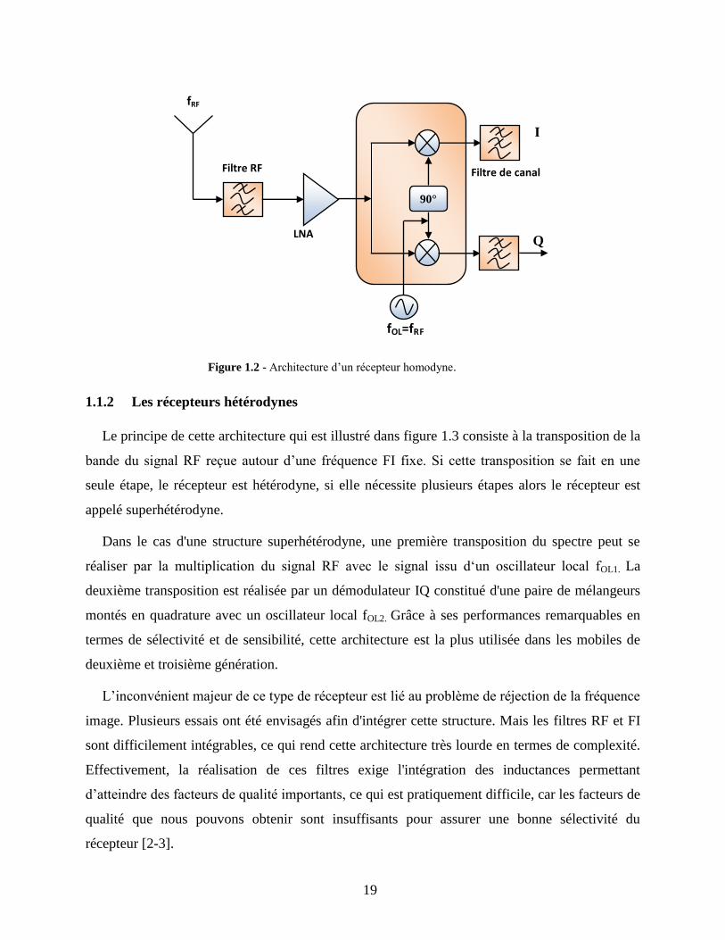
1.1.2 Les récepteurs hétérodynes
Le principe de cette architecture qui est illustré dans figure 1.3 consiste à la transposition de la
bande du signal RF reçue autour d’une fréquence FI fixe. Si cette transposition se fait en une
seule étape, le récepteur est hétérodyne, si elle nécessite plusieurs étapes alors le récepteur est
appelé superhétérodyne.
Dans le cas d'une structure superhétérodyne, une première transposition du spectre peut se
réaliser par la multiplication du signal RF avec le signal issu d‘un oscillateur local fOL1. La
deuxième transposition est réalisée par un démodulateur IQ constitué d'une paire de mélangeurs
montés en quadrature avec un oscillateur local fOL2. Grâce à ses performances remarquables en
termes de sélectivité et de sensibilité, cette architecture est la plus utilisée dans les mobiles de
deuxième et troisième génération.
L’inconvénient majeur de ce type de récepteur est lié au problème de réjection de la fréquence
image. Plusieurs essais ont été envisagés afin d'intégrer cette structure. Mais les filtres RF et FI
sont difficilement intégrables, ce qui rend cette architecture très lourde en termes de complexité.
Effectivement, la réalisation de ces filtres exige l'intégration des inductances permettant
d’atteindre des facteurs de qualité importants, ce qui est pratiquement difficile, car les facteurs de
qualité que nous pouvons obtenir sont insuffisants pour assurer une bonne sélectivité du
récepteur [2-3].
Figure 1.2 - Architecture d’un récepteur homodyne.
Mélangeu
r
Filtre de canal Filtre RF
LNA
I
Q
fOL=fR
F
fRF
90°
F
20
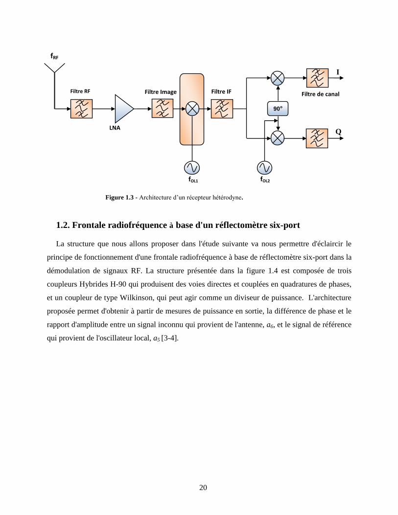
1.2. Frontale radiofréquence à base d'un réflectomètre six-port
La structure que nous allons proposer dans l'étude suivante va nous permettre d'éclaircir le
principe de fonctionnement d'une frontale radiofréquence à base de réflectomètre six-port dans la
démodulation de signaux RF. La structure présentée dans la figure 1.4 est composée de trois
coupleurs Hybrides H-90 qui produisent des voies directes et couplées en quadratures de phases,
et un coupleur de type Wilkinson, qui peut agir comme un diviseur de puissance. L'architecture
proposée permet d'obtenir à partir de mesures de puissance en sortie, la différence de phase et le
rapport d'amplitude entre un signal inconnu qui provient de l'antenne, a6, et le signal de référence
qui provient de l'oscillateur local, a5 [3-4].
Figure 1.3 - Architecture d’un récepteur hétérodyne.
Filtre IF Filtre Image
fOL1
Filtre de canal
I
Q
fOL2
Filtre RF
LNA
fRF
90°

21
Les signaux de sortie, bi, peuvent s'exprimer en fonctions des signaux ai et les paramètres de
dispersion Sij du réflectomètre six-port par la relation linéaire suivante :
Les paramètres Sij du réflectomètre six-port peuvent être obtenus directement à partir de la
figure 1.4. À cet effet, on exploite les matrices de dispersion [S], du coupleur hybride H-90°, et
celle du diviseur de puissance Wilkinson. Les matrices correspondantes sont données dans
l'ordre par les équations (1.2) et (1.3).
Donc, on obtient la matrice [S] globale du réflectomètre six-port de la figure 1.4.
Figure 1.4 - Architecture d'une frontale radiofréquence à base du réflectomètre six-port.

22
À l'aide de l’équation (1.4), nous pouvons conclure les formules des quatre formes d’ondes
émergentes, b1, b2, b3, b4, en fonction des deux ondes incidentes a5 et a6 :
(1.5)
Dans le but de simplifier les calculs, nous allons admettre que les signaux RF, résultant de
l’antenne, a6, et de l’oscillateur local, a5, ont un rapport d’amplitude α, une différence de phase,
Δφ (t) = φ6(t) - φ5 et une différence de fréquence, Δω = ω – ω0. Ces signaux, nous pouvons les
exprimer par les équations suivantes [3] :
En remplaçant les signaux a5 et a6 par leurs expressions dans le système d’équations
précédant, on obtient :

23
Les signaux en bande FI (fréquence intermédiaire) sont les résultats de la connexion des
quatre sorties du réflectomètre six-port à des détecteurs (voir figure 1.4). Nous considérons que
la puissance délivrée en sortie de chaque détecteur idéal, est proportionnelle au carré de la
magnitude du signal RF [4-6].
Sachant que les détecteurs sont identiques (Ki= K), alors :
Afin de générer des signaux IF/ IQ en quadrature, nous allons utiliser des amplificateurs
différentiels dans la bande intermédiaire, aux sorties, 1 et 3, et 2 et 4, (Figure 1.4) :
On procède à une seconde conversion de fréquence suivie par un filtrage basse fréquence, on
obtient les formules des signaux I/Q en bande de base.
24
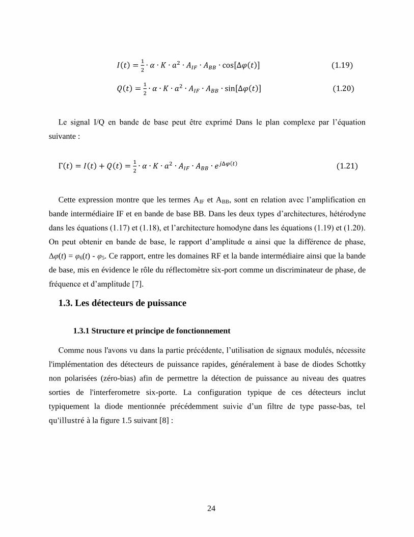
Le signal I/Q en bande de base peut être exprimé Dans le plan complexe par l’équation
suivante :
Cette expression montre que les termes AIF et ABB, sont en relation avec l’amplification en
bande intermédiaire IF et en bande de base BB. Dans les deux types d’architectures, hétérodyne
dans les équations (1.17) et (1.18), et l’architecture homodyne dans les équations (1.19) et (1.20).
On peut obtenir en bande de base, le rapport d’amplitude α ainsi que la différence de phase,
Δφ(t) = φ6(t) - φ5. Ce rapport, entre les domaines RF et la bande intermédiaire ainsi que la bande
de base, mis en évidence le rôle du réflectomètre six-port comme un discriminateur de phase, de
fréquence et d’amplitude [7].
1.3. Les détecteurs de puissance
1.3.1 Structure et principe de fonctionnement
Comme nous l'avons vu dans la partie précédente, l’utilisation de signaux modulés, nécessite
l'implémentation des détecteurs de puissance rapides, généralement à base de diodes Schottky
non polarisées (zéro-bias) afin de permettre la détection de puissance au niveau des quatres
sorties de l'interferometre six-porte. La configuration typique de ces détecteurs inclut
typiquement la diode mentionnée précédemment suivie d’un filtre de type passe-bas, tel
qu'illustré à la figure 1.5 suivant [8] :

25
La caractéristique non linéaire reliant le courant i(t) qui parcourt la diode et la tension RF
d’entrée VRF(t) est généralement décrite par la loi de Schottky. En négligeant la résistance série
parasite de la diode, cette caractéristique sera exprimée par :
Avec :
Is : le courant de saturation, qo : la charge de l’électron, n : le coefficient d’idéalité, K : la
constante de Boltzmann, T : la température.
Sachant que la tension VRF(t) peut exprimée par :
D'autre parts, en considérant que le signal d’entrée VRF(t) est de faible puissance, et qu'il
vérifie la condition : A<VT, alors nous pouvons réexprimer l’équation (1.22) en employant le
développement limité de la fonction exponentielle afin d'obtenir :
Figure 1.5 - Schéma typique d’un détecteur de puissance à base
de diode de type Schottky.

26
Par ailleurs, le circuit basse fréquence équivalent à la sortie du détecteur peut se présenter
comme suit [8-9]:
La résistance dynamique de la diode, correspond à la résistance vidéo RV [8]. Cette dernière
avec la résistance R et le condensateur C forment un filtre passe-bas du premier ordre ayant une
fréquence de coupure fc :
Avec le choix d'une fréquence de coupure fc faible par rapport à la fréquence RF d'entrée du
détecteur, la tension de sortie Vo(t) sera donc proportionnelle aux composantes basses fréquences
ou bande de base (BB) du courant i(t), notamment au terme quadratique de l’équation (1.24).
Alors, par le remplacement de l’expression de la tension d’entrée RF donnée par (1.23) dans
l’équation (1.24), et en ne tenant compte que du terme quadratique de l'équation, nous obtenons
donc :
Figure 1.6 - Schéma équivalent de la sortie du détecteur à base
de diode Schottky.
27
Après une opération de filtrage passe-bas, la tension de sortie sera alors :
Le coefficient α représente la sensibilité du détecteur qui est habituellement exprimée en
Volt/Watt. D'après la formule, on peut constater que pour les faibles niveaux de puissance, le
détecteur à diode réalise une détection de puissance, car la tension de sortie du détecteur est
proportionnelle au carré de l’amplitude du signal d’entrée, autrement dit à la puissance du signal
RF. Cependant sur une large plage dynamique de puissance, la caractéristique du détecteur à
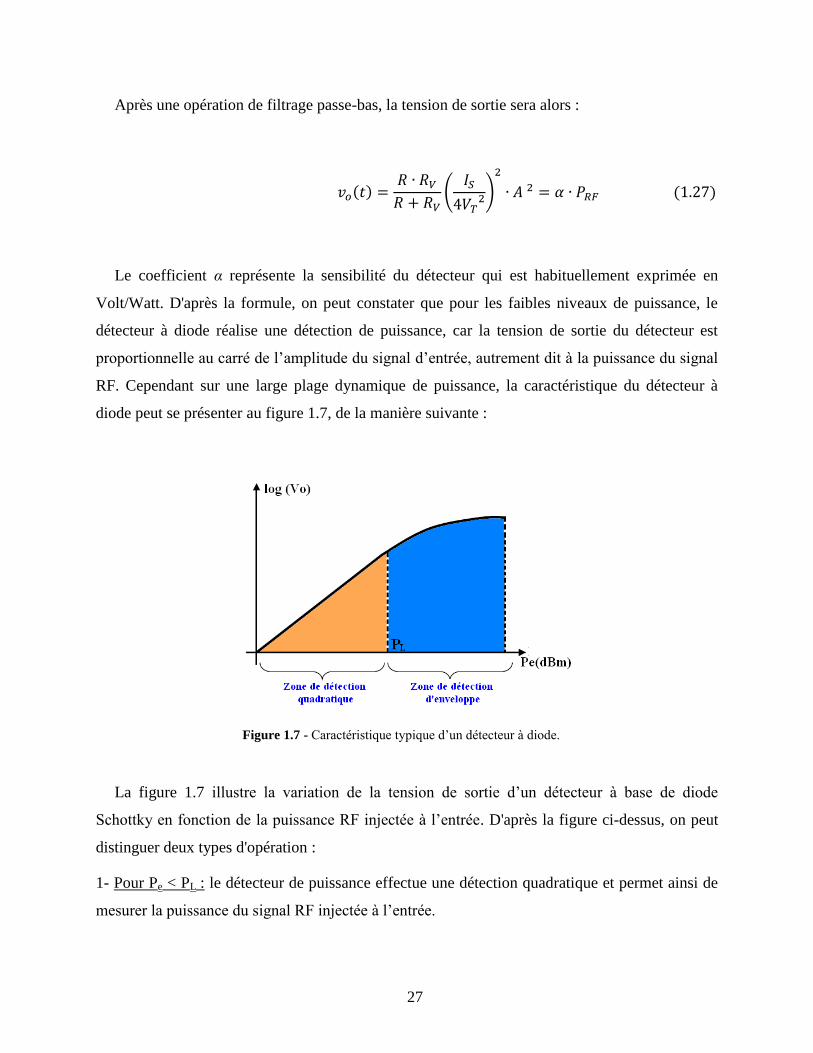
diode peut se présenter au figure 1.7, de la manière suivante :
La figure 1.7 illustre la variation de la tension de sortie d’un détecteur à base de diode
Schottky en fonction de la puissance RF injectée à l’entrée. D'après la figure ci-dessus, on peut
distinguer deux types d'opération :
1- Pour Pe < PL : le détecteur de puissance effectue une détection quadratique et permet ainsi de
mesurer la puissance du signal RF injectée à l’entrée.
Figure 1.7 - Caractéristique typique d’un détecteur à diode.

28
2- Pour Pe >PL : étant donné que la puissance d'entrée est plus élevée, les estimations faites
antérieurement ne sont plus valables, alors la diode fonctionne en mode redresseur, et le
détecteur de puissance réalise une détection d’enveloppe classique. Dans de tel cas, une
correction de la tension de sortie est nécessaire afin d’augmenter la dynamique de mesure de
puissance [8].
1.4. Les amplificateurs à faible bruit (LNAs)
1.4.1 Principe de fonctionnement et utilité
Un amplificateur à faible bruit ou LNA (Low Noise Amplifier) représente l'amplificateur de
tête de la chaine de réception. Il est souvent placé à proximité de l'antenne, afin d‘amplifier les
signaux utiles ayant un très faible niveau puissance à la sortie de cette dernière. Cependant,
l'amplification du signal reçu par l'amplificateur doit répondre à deux critères importants :
maintenir un gain stable et approprié tout en contrôlant la dégradation de la figure de bruit du
récepteur. Autrement dit, un compromis entre le facteur de bruit et le gain est donc nécessaire
dans la conception du LNA [1].
Généralement, le facteur de bruit F représentant la dégradation du rapport signal à bruit causé
par les composants de la chaîne RF. Il est défini comme étant le rapport entre les SNR (Signal-
to-Noise Ratio) à l'entrée et à la sortie du bloc :
Habituellement dans le domaine des télécommunications, il est commun d'utiliser comme
unité le décibel (dB), alors, dans ce cas, le facteur de bruit est plus communément nommé figure
de bruit NF (Noise Figure), et il peut être s'exprime comme suit :
Par ailleurs, la figure de bruit globale d'une telle chaîne peut être déterminée par la formule de
Friis (1.30). Cette dernière montre que plus le gain d'un amplificateur en amont est élevé, plus

29
son influence sur le bruit global est significative. La conception d'un LNA doit donc être un
compromis entre le facteur de bruit et le gain.
1.4.2 Spécifications typique d'un LNA à 60 GHz
Dans le cadre de notre projet de thèse, nous avons opté pour le LNA (TGA4600) de la
compagnie TriQuint. Ce dernier possède un facteur de bruit acceptable NF = 4 dB, ce qui permet
de limiter significativement la contribution en bruit de la chaine de réception. Un exemple de
l'implantation de cet amplificateur faible bruit LNA sur un substrat en céramique utilisant la
technologie MHMIC est illustré dans la figure 1.8. Les caractéristiques typiques à 60 GHz afin
qu'il remplisse adéquatement son rôle sont également présentées au tableau 1 :
1.4.3 Problématique de la composante continue ou “DC offset”
La génération de composantes continues ou DC offset est une problématique très courante
dans les récepteurs homodynes. Ces composantes apparaissent d'une manière directe dans la
bande utile comme des signaux parasites.
Ce phénomène est généralement le résultat de deux principaux facteurs, le premier, est le
niveau d'isolations entre l’OL (Oscillateur Local), les entrées du mélangeur et le LNA. En effet,
Tableau 1.1- Caractéristiques typiques d'un LNA à 60 GHz
Technologie 0.15 um 3MI pHEMT
NF 4 dB
Gain 13 dB
Bande de fréquence 57 - 65 GHz
Impédance d'entrée et de sortie 50 Ω
Taux de retour en entrée et en sortie 26 dB et 6 dB
Isolation inverse 20 dB
Facteur de stabilité >1
Figure 1.8 - Exemple d'implantation
d'un LNA à 60 GHz (TGA4600)
diode.

30
cette isolation n'est pas idéale, et par conséquent, une fuite provenant de l’OL peut avoir lieu.
Cette dernière est généralement due au couplage direct ou indirect par le substrat et elle peut
apparaître également à l’entrée du LNA et même parfois à l’entrée du mélangeur.
Ce problème est représenté dans la figure 1.9 où uniquement la voie Q est considérée. Cette
fuite liée à l’OL est présentée à l’entrée du LNA et du mélangeur, est par la suite mélangée avec
le signal provenant de l’OL lui-même, pour générer une composante parasite autour de la
fréquence zéro (DC composante) [1] [11].
Par ailleurs, le même phénomène peut se reproduire quand les fortes interférences présentent
sur l’antenne peuvent traverser le LNA pour se rendre aux entrées du mélangeur et ensuite se
multiplier avec lui-même [1][10]. La figure 1.10 illustre bien ce phénomène, où qu'une seule
voie Q est considérée.
Figure 1.9 - Problème de la fuite d'oscillateur local (OL)
dans une chaîne de réception homodyne.
Figure 1.10 - Problème de fuite des signaux parasites vers
l'oscillateur local (OL) dans une chaîne de réception homodyne.
31
1.5. Le réseau d’antennes
1.5.1 Généralités
L’antenne est un dispositif permettant de rayonner (émission) ou de capter (réception) des
ondes électromagnétiques. Elle sert d’interface entre les ondes électromagnétiques qui se
propagent dans les structures de guidages (guides d’ondes, lignes de transmission) et les ondes
qui se propagent dans l’espace libre [12].
Le choix d’un type d’antenne dépend surtout du type d’application envisagée. Les facteurs les
plus fondamentaux à considérer dans une antenne sont entre autres, la puissance d’émission qui
fixe la portée du système, la directivité, la taille et la facilité d’intégration de l’antenne dans un
système complet.
Il existe plusieurs types d’antennes, les antennes filaires, les antennes patchs et les antennes à
ouverture. Ces derniers ont été considérées pendant longtemps comme les seules susceptibles de
montrer de bonnes performances pour les applications en ondes millimétriques. Cependant, de
récents développements ont montré que les antennes patchs disposent également de très bonnes
performances aux fréquences millimétriques [13-14].
Pour les applications millimétriques sans fil, courtes distances et haut débit, ces antennes
répondent parfaitement à nos exigences en termes de coût de production, de taille, et de facilité
d’intégration dans le prototype de frontale radiofréquence réalisé en technologie MHMIC.
1.5.2 Directivité, Efficacité et Gain
La directivité d’une antenne désigne généralement la façon dans laquelle une antenne
concentre son rayonnement dans certaines directions de l’espace. Elle est définie comme le
rapport entre l’intensité de rayonnement (U (θ, ϕ)) dans une direction donné et l’intensité de
rayonnement moyenne d’une antenne isotrope (U0). La densité de rayonnement de cette dernière
est égale à la puissance rayonnée par l’antenne (PR) divisée par 4π [12].

32
Alors, la directivité est une grandeur qui permet de décrire le rayonnement de l’antenne par
rapport à un rayonnement isotrope. Donc, plus l’antenne est directive, plus le rayonnement est
dirigé vers une seule direction.
L’efficacité totale d’une antenne est employée pour prendre en compte les pertes à l’entrée du
dispositif et les pertes liées aux conducteurs. Elle est égale au rapport entre la puissance rayonnée
(PRay) et la puissance incidente à l’entrée de l’antenne (PI). Ce rapport est souvent utilisé pour
prendre en considération les pertes de l’antenne incluant, la puissance perdue dans la
métallisation (effet Joule) ou dans le substrat, et la puissance réfléchie à l’entrée en raison de la
désadaptation d’impédance de l’antenne. En générale, à part de l’efficacité totale, nous parlons
également de l’efficacité de rayonnement qui traduit le rapport entre la puissance rayonnée et la
puissance transmise à l’antenne (PT). Toutes ces puissances sont illustrées, ci-dessous, à la figure
1.11.
ηref représente la désadaptation de l’impédance d’entrée de l’antenne (Zin) et la source (Z0). Γ
est le coefficient de réflexion à l’entrée de l’antenne et est donné par [15] :
Figure 1.11 - Efficacité de rayonnement et efficacité de l’antenne

33
Le gain d’une antenne, dans une direction donné, est défini comme le rapport de l’intensité de
rayonnement de l’antenne, par l’intensité de rayonnement d’une antenne isotrope idéale, dans
cette direction. Les deux antennes sont supposées être alimentées par la même puissance. Cette
expressions se résume à [15]:
Ainsi, le gain est lié à la directivité par l’intermédiaire de l’efficacité :
Références
[1] Ioan BURCIU, 2010. “Architecture de récepteurs radiofréquences dédiés au traitement
bibande simultané”. Thèse de doctorat, l’Institut National des Sciences Appliquées de Lyon,
210p.
[2] Moussa Hassan BARAKAT, 2008. “Dispositif radiofréquence millimétrique pour objets
communicants de type smart dust”. Thèse de doctorat, Institut de Microélectronique,
Electromagnétisme et Photonique, INPG, MINATEC, 212p.
[3] Tatu, S.O. 2005. “Nouveau récepteur six-port en ondes millimétriques”. Thèse de doctorat,
Montréal, École polytechnique, 209p.
[4] Li, J., R.G. Bosisio et K. Wu. 1995. “Computer and Measurement Simulation of a New
Digital Receiver Operating Directly at Millimeter-Wave Frequencies”. IEEE Transactions
Microwave Theory Techniques, 43, 2766-2772.
[5] Engen, G.F. et C.A. Hoer. 1972. “Application of an Arbitrary 6-Port Junction to Power-
Measurement Problems”. IEEE Trans. Instrumentation and Measurement, IM-21, 470-474.

34
[6] Engen, G.F. 1977. “The Six-Port Reflectometer: An Alternative Network Analyzer". IEEE
Trans. Microwave Theory Technique, MTT-25, 1075-1077.
[7] Tatu, S. O., E. Moldovan, K. Wu, R. G. Bosisio. et T. Denidni, (2005). “Ka-Band Analog
Front-End for Software-Defined Direct” Conversion Receiver. IEEE Transactions on Microwave
Theory and Techniques, vol. 53, no 9, 2678 - 2776.
[8] Sara ABOU CHAKRA, 2004. “La Boucle Locale Radio et la Démodulation directe de
signaux larges bandes à 26 GHz”. Thèse de doctorat, Télécom ParisTech ENST, 144p.
[9]Woods, D. 1979. “Analysis and calibration theory of the general six-port reflectometer
employing four amplitude detector”, Pro IEEE, Vol. 126, pp. 221-228.
[10] Fredrick, JD; T. Itoh. 2001. “Recent developments in RF front ends based upon active
antenna concepts”. TELSIKS 2001, pp. 3-9.
[11] Fredrick, J.D., Y. Qian et T. Itoh. 2000. “Novel Design Technique for A Low Noise
Receiver Front End With Integrated Circularly Polarized Patch Antenna”. 30th European
Microwave, Conference Proceedings, vol. 2 pp. 333-336.
[12] Stutzman W. L., et G.A. Thiele. 1981. Antenna Theory and Design, John Wiley, New York.
[13] Park, J., Y. Wang et T. Itoh. 2003. “A 60GHz Integrated Antenna Array for High-Speed
Digital Beamforming Applications”. Microwave Symposium Digest, 2003 IEEE MTT-S
International, vol. 3, pp. 1677-1680.
[14] J.R. JAMES & P.S. HALL, (1989).Handbook of Microstrip Antennas Volume 1. Peter
Peregrinus ltd., London UK
[15] Lee, K.F. and Chen, W., (1997). Advances in Microstrip and Printed Antennas John
WILEY & Sons, Inc.

35
CHAPITRE 2 :
COMPLETE CHARACTERIZATION OF NOVEL MHMICS FOR V BAND COMMUNICATION SYSTEMS
C. Hannachi, D. Hammou, T. Djerafi, Z. Ouardirhi, and S.O. Tatu
Journal of Electrical and Computer Engineering, vol. 2013, pp.1-7, October 2013
Résumé : Dans ce chapitre nous avons présenté les différents circuits passifs conçus pour
opérer à la bande de fréquence de 60 GHz en adoptant la technologie MHMIC
(Miniaturized Hybrid Microwave Integrated Circuit). Ces circuits incluent, le coupleur
hybride H90o, le coupleur en anneau (rat-race), le diviseur de puissance de type Wilkinson
et enfin l'interféromètre six-port qui sera la combinaison d'un diviseur de puissance et trois
coupleurs hybrides H90o. Tous ces circuits ont été caractérisés expérimentalement en
termes de paramètres de despertion S dans la bande millimétrique considérée, de 60 à 65
GHz. Comme technique de calibration, nous avons opté pour la calibration TRL (Thru,
Reflect, Line) où nous avons préféré fabriquer notre propre kit de calibration et de
l'intégré avec les circuits à caractériser. Cette démarche nous permet d'éviter l'utilisation
des standards commerciaux (ISS), connus pour leurs coûts trop élevés et qui sont conçus
généralement sur un différent standard de substrat. Cette première fabrication est
considérée comme une étape préliminaire essentielle à la conception de notre futur
prototype de la frontale radiofréquence, car elle nous permet de connaitre avec exactitude
les performances de l'interféromètre six-port, utilisé comme un démodulateur direct en
bande millimétrique.

36
Abstract
This paper presents the characterization results of several new passive millimeter wave
circuits integrated on very thin ceramic substrate. The work is focused on the design and
characterization of a novel rounded Wilkinson power divider, a 90° hybrid coupler, a rat-race
coupler, and of a novel six-port (multi-port) circuit. Measurements show the wideband
characteristics, allowing therefore their use for multi Gb/s V-band wireless communication
systems.
2.1. Introduction
THE use of the 60-GHz band has attracted a great deal of interest over the last few decades,
especially for its use in future compact transceivers dedicated to high-speed wireless applications
in indoor environments (57 – 64 GHz) [1], [2], [3]. In this context, intensive research have been
done to further develop new millimeter-wave components for high data rate wireless
communications according to the IEEE 802.15.3c standard. As previously demonstrated, the six-
port technology offers an excellent alternative to conventional receiver architectures ,
especially at millimeter-wave frequencies [4], [5], [6].
Nowadays, there are few promising high-quality fabrication technologies, yielding potentially
low-cost millimeter-wave components, such as the Monolithic Microwave Integrated Circuit
(MMIC) on GaAs or SiGe for large-scale production, and the Miniature Hybrid Microwave
Integrated Circuit (MHMIC) technology on very thin ceramic substrates, for small-scale
production and prototyping [7], [8].
Moreover, several technologies have been intensively used for the millimeter wave circuit
design and in house prototype fabrication. We particularly note the coplanar, the Substrate
Integrated Waveguide (SIW), and the microstrip technology. The coplanar technology assures
high-quality component design, but is not well suited for low-cost production due to the
difficulties in automating wire-bonding implementation, necessary for obtaining repeatable
performances. On the other hand, the SIW technology assures high-quality component design on
thin ceramics [9] or the design of optimal transitions from planar to standard rectangular
waveguides [10]. For further circuit miniaturization, the microstrip technology on very thin, high
relative permittivity substrate is recommended.

37
As know, the microstrip line width is related to the characteristic impedance, substrate relative
permittivity and its thickness. It is to be noted that, due to reduced guided wavelength in high
permittivity ceramic substrates, in order to keep the required circuit aspect ratio (guided
wavelength versus the line width), the substrate must be as thin as possible. The optimal choice
for frequencies greater than 60 GHz is the 127 µm thick alumina substrate, which is also easily
compatible with the usual 100 µm thick MMIC active components, to be integrated with planar
passive MHMICs. The MMIC chips are placed in rectangular cuts on ceramics, on the top of the
same metallic fixture, allowing thermal dissipation and easy wire-bonding with MHMIC
components, which are practically at the same height.
Initial designs and circuit characterization results of several MHMIC passive circuits on very
thin ceramic substrate, designed for advanced millimeter wave systems operating in 60 – 90 GHz
band, have been published few years ago [11].
This paper presents novel circuit designs, together with major improvements obtained in
fabrication and characterization process in recent years.
2.2. Calibration Techniques and Standards
Measurement performance mainly depends on the accuracy of the calibration technique and
its standards used for correcting the imperfections of the measurement system. These
imperfections depend on several factors such as non-ideal nature of cables and probes, and the
internal characteristics of the vector network analyzer (VNA) itself. In order to simplify
calibration procedures and to obtain more accurate and reliable measurement by introducing
much smaller systematic errors, the on-wafer calibration and measurement with pico-probes
were adopted.
Typically, on-wafer calibration standards are fabricated either on the wafer including the
device under test (DUT) or on a separate impedance standard substrate (ISS). The reference
plane is usually taken at the probe tips. Nevertheless, for the DUT measurement in microstrip
technology, on-wafer standards fabricated on the same wafer as the DUT are required since the
probe-to-standard transition can be designed to be very similar to the transition to the DUT. It
sometimes happens that the transition between the probe tips and the coplanar line end is not
well matched and parasitic and some wave modes occur at the contact of the probe tips. By

38
taking the probe tips as measurement reference plane, the errors due to this transition are not
corrected, and may affect the measurement results.
Different calibration procedures or standards have been used for measuring microstrip based
circuits; among the most commonly used are line-reflect-match (LRM), line-line-reflect-match
(LLRM), and thru-reflect-line (TRL) [12].
One of the most robust and popular technique is the TRL calibration, that is well suited to the
on-wafer measurements at millimeter wave frequencies. According to previous comments, the
reference plane is considered at the middle of the thru line. The TRL calibration was done using
on-wafer microstrip structures and the TRL algorithm supported by our vector network analyzer
E8362B of Agilent Technologies.
A non-zero length thru is used to extend the reference plane a physical distance of 2286 µm
into the microstrip line in order to ensure direct measurement at the desired reference plane of
the device, eliminating further de-embedding and its associated uncertainties.
One microstrip delay line of 477 µm length is used to cover the whole considered frequency
band. Generally, in order to avoid phase uncertainties, for TRL calibration, the electrical length
of the line standard is maximum 180° at the highest operating frequency.
For the reflect standard, the designer can chose between the open and the short. In our
opinion, the open standard is a better option at millimeter wave frequencies, due to the complex
nature of the short circuit design having repeatable performances in microstrip technology,
especially when via-holes are used.
In our designs, millimeter wave RF short circuits are implemented with quarter wavelength
sectors, avoiding via-holes.
Figure 2.1 shows a microphotograph of typical fabricated circuits, including several identical
TRL standard calibration kits. In order to optimize the fabrication cost and the
measurement time, a maximum number of circuits to be characterized are fabricated on
each ceramic die of 2.54 cm x 2.54 cm.
Due to the vulnerability of the very thin gold layer metallization (1 μm), multiple identical
kits have been fabricated in order to ensure successful calibration before each measurement.
Small microstrip conductor areas were also added on die in order the properly align the pico-

39
probes before measurement. In addition, 50 Ω microstrip terminations and resistors test kits,
were used to verify the required value of 100 Ω per square for the integrated loads.
Typical measurement results over 60 – 90 GHz band of a microstrip line, after calibration,
show matching results better than -50 dB at both ports, and a quasi-perfect transmission of 0 dB
(with no more than 0.5 dB ripple, the intrinsic error of the VNA) when the pico-probes are
properly aligned and positioned.
2.3. Basic Circuit Characterization
In order to integrate complete millimeter wave front-ends on ceramic substrates, the first step
is to design basic circuits, such as couplers and power dividers/combiners. These components
will be further utilized in antenna array and six-port down-converter or direct modulator designs.
As mentioned, the MHMICs have been designed and fabricated on a very thin ceramic
substrate having a relative permittivity of 9.9 and a thickness of 127 µm. Advanced Design
System (ADS) version 2011.05 of Agilent Technologies was used for circuits design and
Figure 2.1 - Microphotograph of the fabricated circuits on thin ceramic
substrate of 2.54 cm x 2.54 cm.

40
simulation. In order to perform on-wafer measurement of the S parameters, several circuits have
been integrated in the same alumina substrate of 2.54 cm x 2.54 cm size, as see in Figure 2.1.
The symmetry of circuits is used to reduce the number of fabricated circuits required for
complete characterization. For example, the full characterization of four port couplers requires
minimum three different circuits due to the two-dimensional symmetry. Only two circuits are
needed for the Wilkinson power divider, because of its one-dimension symmetry. Finally, five
circuits are requested for the full characterization of our six-port design. All these circuits can be
easily identified in Figure 2.1. The unused ports are connected to integrated 50 Ω loads.
Even if the allowed frequency band starts from 57 GHz, all circuits are measured from 60
GHz because of measurement set-up capabilities (WR-12 rectangular waveguides modules for
the 60 – 90 GHz millimeter wave extension of the VNA). However, the results can be
extrapolated in the 57 – 60 GHz band by symmetry and comparison with electromagnetic
simulations.
2.3.1. 90° Hybrid Coupler
Figure 2.2 shows the microphotograph of the 90o hybrid coupler, prepared for port 1 to port 3
measurements
As usual in our millimeter wave designs, the shape of the circuit is rounded, ensuring better S
parameter performances. The microstrip line widths are 126 μm for the 50 Ω microstrip line, 100
μm for central line of the coplanar input, and 250 μm for 50/ Ω quarter wave line inside the
Figure 2.2 - Microphotograph of the branch-line coupler

41
coupler. The diameter of the coupler, measured between the centers of diametrically opposite
microstrip lines is around 625 μm.
As explained earlier, all via-holes are replaced by wide-band RF short circuits. Details, such
as 50 Ω integrated resistor or the trace of the pico-probes on gold layer metallization after
measurement, can be seen in the picture.
Figures 2.3 to 2.5 show measurement results for S parameter magnitudes and phases of the
circuit. Measurements are performed for S21, S31, and S41 on three different circuits (see Figure
2.1, the secondary diagonal).
Figure 2.3 - Measured input return loss for the 90° hybrid coupler.

42
As seen in Figure 2.3, the measured return losses are better than 26 dB at 60 GHz, and better
than 14 dB at the highest frequency allowed for V-band communications, 64 GHz.
The isolation, S41, is around 20 dB at 60 GHz and has comparable values with return losses
from 63 GHz. The measured transmitted power is well splitted between the two outputs,
especially around the central frequency allowed for V-band communications (60.5 GHz). The
magnitude unbalancing is practically zero at 60 GHz and less than 1 dB at 64 GHz, as it can be
seen in Figure 2.4.
Figure 2.4 - Measured transmission S parameter magnitudes for the 90°
hybrid coupler.
Figure 2.5 - Measured transmission S parameter phase difference for the
90° hybrid coupler.
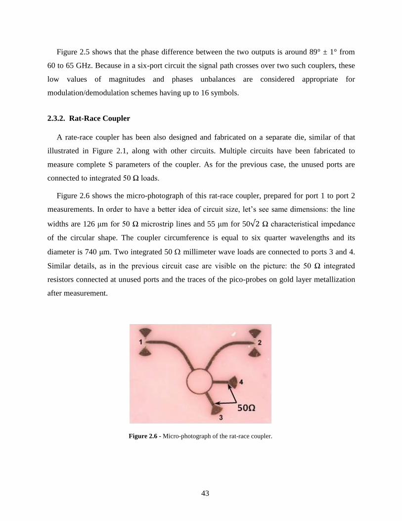
43
Figure 2.5 shows that the phase difference between the two outputs is around 89° ± 1° from
60 to 65 GHz. Because in a six-port circuit the signal path crosses over two such couplers, these
low values of magnitudes and phases unbalances are considered appropriate for
modulation/demodulation schemes having up to 16 symbols.
2.3.2. Rat-Race Coupler
A rate-race coupler has been also designed and fabricated on a separate die, similar of that
illustrated in Figure 2.1, along with other circuits. Multiple circuits have been fabricated to
measure complete S parameters of the coupler. As for the previous case, the unused ports are
connected to integrated 50 Ω loads.
Figure 2.6 shows the micro-photograph of this rat-race coupler, prepared for port 1 to port 2
measurements. In order to have a better idea of circuit size, let’s see same dimensions: the line
widths are 126 μm for 50 Ω microstrip lines and 55 μm for 50 Ω characteristical impedance
of the circular shape. The coupler circumference is equal to six quarter wavelengths and its
diameter is 740 μm. Two integrated 50 millimeter wave loads are connected to ports 3 and 4.
Similar details, as in the previous circuit case are visible on the picture: the 50 Ω integrated
resistors connected at unused ports and the traces of the pico-probes on gold layer metallization
after measurement.
Figure 2.6 - Micro-photograph of the rat-race coupler.

44
Figures 2.7 to 2.9 show measurement results for S parameter magnitudes and phases of this
rat-race coupler. Figure 2.7 shows the measured input return loss and isolation values are better
than 15 dB over the whole considered frequency band, from 60 to 65 GHz. The isolation S14
reaches an exceptional value, of at least 35 dB, due to the constant characteristic impedance over
the ring. There are no steps in line width, which improves millimeter wave isolation. As regards
with the transmitted power plotted in Figure 2.8, a quasi-equal split between the two outputs over
the whole frequency range of interest is observed. The measured unbalancing is less than 0.5 dB,
comparable with the intrinsic error of the VNA.
Figure 2.9 shows the measurement of the transmission phase difference between the output
ports. The phase difference value is equal to 180°, with a corresponding of phase error of ± 5° over the
considered frequency band. This error is close to 0° at the central frequency allowed for V-band
communications (60.5 GHz).
Figure 2.7 - Measured input return loss for the rat-race coupler.
Figure 2.8 - Measured transmission S parameter magnitudes for
the rat-race coupler.
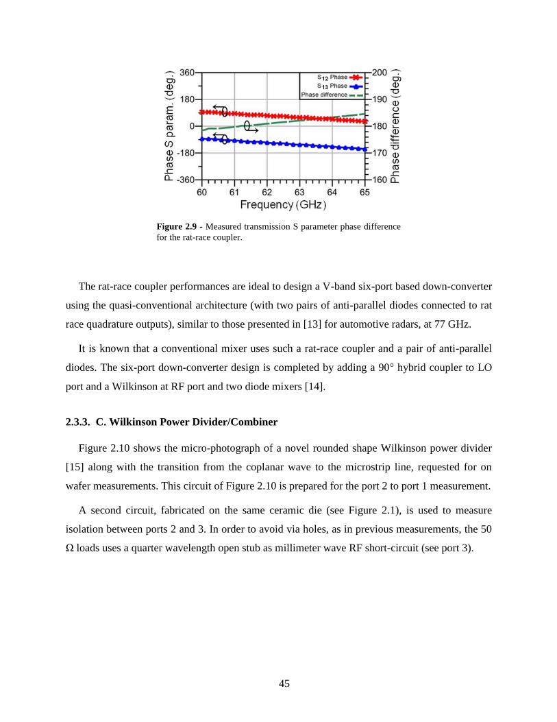
45
The rat-race coupler performances are ideal to design a V-band six-port based down-converter
using the quasi-conventional architecture (with two pairs of anti-parallel diodes connected to rat
race quadrature outputs), similar to those presented in [13] for automotive radars, at 77 GHz.
It is known that a conventional mixer uses such a rat-race coupler and a pair of anti-parallel
diodes. The six-port down-converter design is completed by adding a 90 hybrid coupler to LO
port and a Wilkinson at RF port and two diode mixers [14].
2.3.3. C. Wilkinson Power Divider/Combiner
Figure 2.10 shows the micro-photograph of a novel rounded shape Wilkinson power divider
[15] along with the transition from the coplanar wave to the microstrip line, requested for on
wafer measurements. This circuit of Figure 2.10 is prepared for the port 2 to port 1 measurement.
A second circuit, fabricated on the same ceramic die (see Figure 2.1), is used to measure
isolation between ports 2 and 3. In order to avoid via holes, as in previous measurements, the 50
Ω loads uses a quarter wavelength open stub as millimeter wave RF short-circuit (see port 3).
Figure 2.9 - Measured transmission S parameter phase difference
for the rat-race coupler.
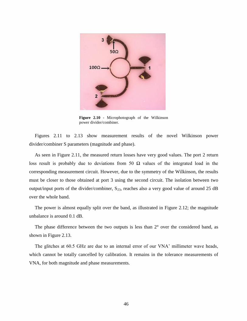
46
Figures 2.11 to 2.13 show measurement results of the novel Wilkinson power
divider/combiner S parameters (magnitude and phase).
As seen in Figure 2.11, the measured return losses have very good values. The port 2 return
loss result is probably due to deviations from 50 Ω values of the integrated load in the
corresponding measurement circuit. However, due to the symmetry of the Wilkinson, the results
must be closer to those obtained at port 3 using the second circuit. The isolation between two
output/input ports of the divider/combiner, S23, reaches also a very good value of around 25 dB
over the whole band.
The power is almost equally split over the band, as illustrated in Figure 2.12; the magnitude
unbalance is around 0.1 dB.
The phase difference between the two outputs is less than 2° over the considered band, as
shown in Figure 2.13.
The glitches at 60.5 GHz are due to an internal error of our VNA’ millimeter wave heads,
which cannot be totally cancelled by calibration. It remains in the tolerance measurements of
VNA, for both magnitude and phase measurements.
Figure 2.10 - Microphotograph of the Wilkinson
power divider/combiner.
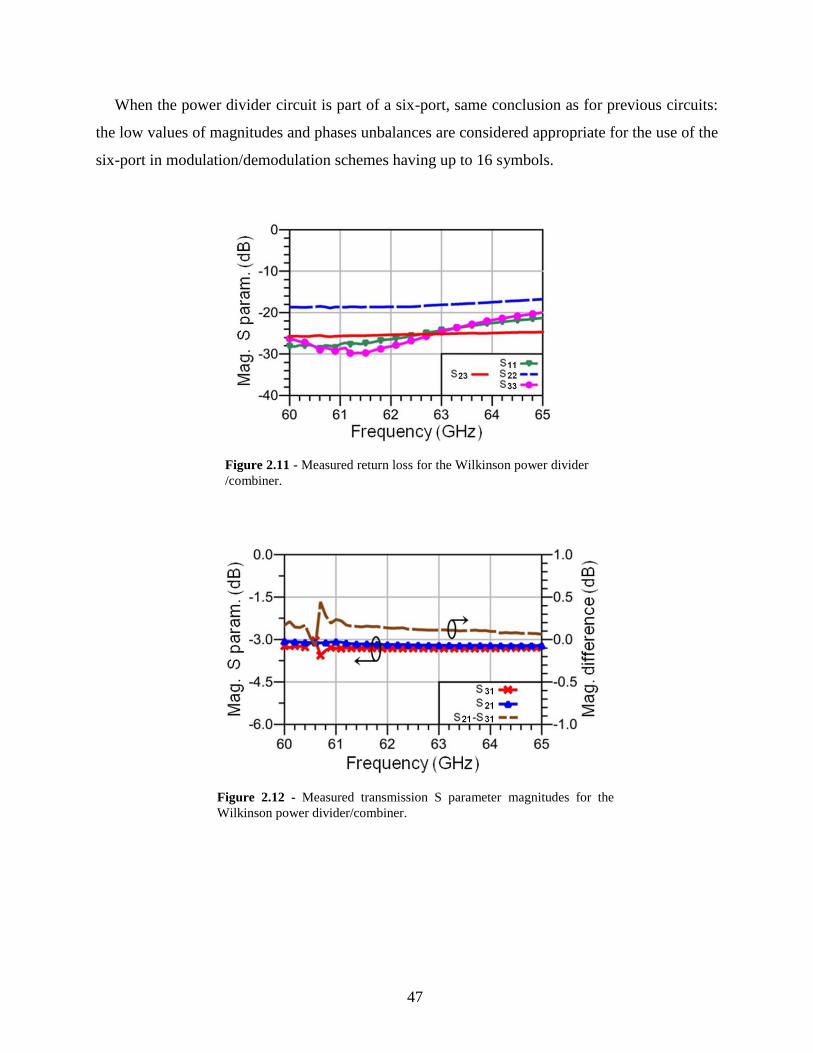
47
When the power divider circuit is part of a six-port, same conclusion as for previous circuits:
the low values of magnitudes and phases unbalances are considered appropriate for the use of the
six-port in modulation/demodulation schemes having up to 16 symbols.
Figure 2.11 - Measured return loss for the Wilkinson power divider
/combiner.
Figure 2.12 - Measured transmission S parameter magnitudes for the
Wilkinson power divider/combiner.

48
2.4. Six-port Circuit Characterization
Six-port (multi-port) quadrature down-conversion and direct modulation is an innovative
approach in millimeter wave technology. A complete theory, validated by various simulations
and measurements of V-band direct conversion receivers, has been published in recent years
[14], [16].
Figure 2.14 shows the block diagram of the proposed six-port, composed by a Wilkinson
power divider and three 90° hybrid couplers. As usually noted in all our previous publications, in
a six-port down converter, the port 6 is connected to the RF signal and the port 5 is connected to
the LO signal; the other four output ports (1, 2, 3, and 4) are connected to power detectors [14].
Figure 2.13 - Measured transmission S parameter phase difference for the
Wilkinson power divider/combiner
Figure 2.14 - Six-port circuit block diagram.
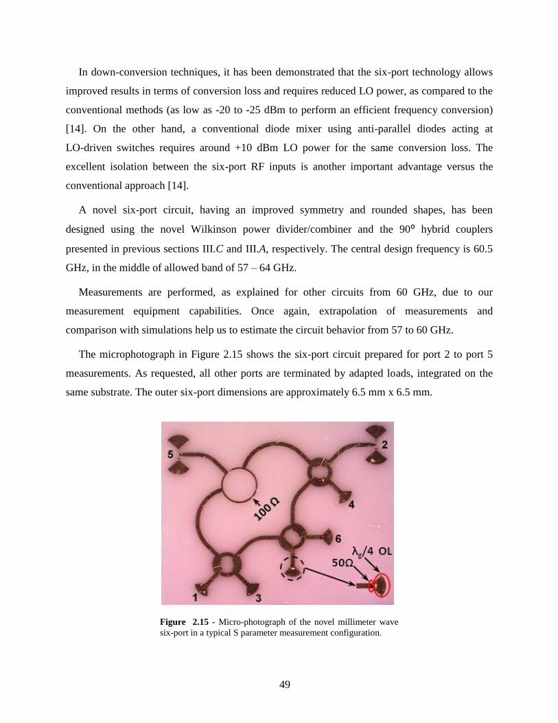
49
In down-conversion techniques, it has been demonstrated that the six-port technology allows
improved results in terms of conversion loss and requires reduced LO power, as compared to the
conventional methods (as low as -20 to -25 dBm to perform an efficient frequency conversion)
[14]. On the other hand, a conventional diode mixer using anti-parallel diodes acting at
LO-driven switches requires around +10 dBm LO power for the same conversion loss. The
excellent isolation between the six-port RF inputs is another important advantage versus the
conventional approach [14].
A novel six-port circuit, having an improved symmetry and rounded shapes, has been
designed using the novel Wilkinson power divider/combiner and the 90⁰ hybrid couplers
presented in previous sections III.C and III.A, respectively. The central design frequency is 60.5
GHz, in the middle of allowed band of 57 – 64 GHz.
Measurements are performed, as explained for other circuits from 60 GHz, due to our
measurement equipment capabilities. Once again, extrapolation of measurements and
comparison with simulations help us to estimate the circuit behavior from 57 to 60 GHz.
The microphotograph in Figure 2.15 shows the six-port circuit prepared for port 2 to port 5
measurements. As requested, all other ports are terminated by adapted loads, integrated on the
same substrate. The outer six-port dimensions are approximately 6.5 mm x 6.5 mm.
Figure 2.15 - Micro-photograph of the novel millimeter wave
six-port in a typical S parameter measurement configuration.

50
In order to measure the most important six-port S parameters (such as RF – LO ports isolation
S65, input match at ports, power transmission between the RF and LO ports to the outputs, and
the phase difference between transmitted signals), five six-port circuits have been integrated in
the same alumina die, along with other basic circuits and required calibration standards (see
Figure 2.1).
Figures 2.16 to 2.21 show some typical measurement results, according to the port numbers
specified in Figures 2.14 and 2.15.
Figure 2.16 shows the measured return loss at port 6 (RF input) and port 5 (LO input), and
isolation between them. At the central operating frequency of V-band systems all values are
better than 20 dB. In addition, the measured values are better than 15 dB at the highest frequency
allowed for V-band communications, 64 GHz.
Figure 2.17 shows the power splitting between the LO port and two adjacent output ports, S25
and S45. As compared to the theoretical value of -6 dB, very good results are obtained over the
band. The supplementary insertion loss is around 1 dB at the central frequency and reaches 1.5
dB at the edge. The magnitude unbalance is close to 0 dB at 62.5 GHz and less than 0.5 dB over
the entire band.
Figure 2.16 - Measured RF inputs return loss and isolation for the
proposed six-port
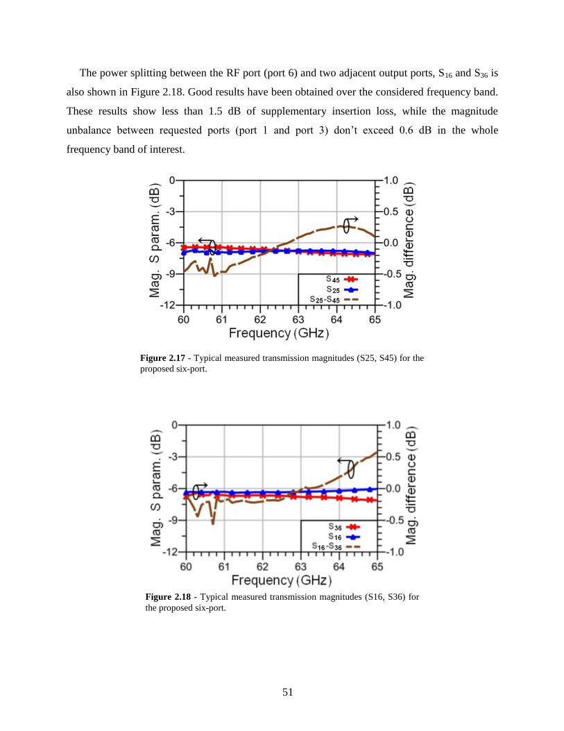
51
The power splitting between the RF port (port 6) and two adjacent output ports, S16 and S36 is
also shown in Figure 2.18. Good results have been obtained over the considered frequency band.
These results show less than 1.5 dB of supplementary insertion loss, while the magnitude
unbalance between requested ports (port 1 and port 3) don’t exceed 0.6 dB in the whole
frequency band of interest.
Figure 2.17 - Typical measured transmission magnitudes (S25, S45) for the
proposed six-port.
Figure 2.18 - Typical measured transmission magnitudes (S16, S36) for
the proposed six-port.

52
The measured return losses at output ports are illustrated in Figure 2.19. At the central
operating frequency of V-band systems all values are better than 25 dB, keeping good values
over the band.
Figure 2.20 shows the phase difference between the two typical transmission S parameters,
S52 and S54. It can be seen that the measured phase difference between these two outputs is close
to the quadratic reference of 90°, as expected. The observed phase difference error is less than ±
2° up to 64 GHz.
As regards the phase difference between the two typical transmission S parameters, S61 and
S63, depicted in Figure 2.21, shows two quasi-parallel characteristics. The phase difference
between two requested ports (port 1, port 3) is closed to 90°. The phase difference error is
approximately 3° in the entire frequency band of interest.
Figure 2.19 - Typical measured outputs matches for the proposed
six-port.
Figure 2.20 - Typical measured transmission phase difference of (S52,
S54) for the proposed six-port.
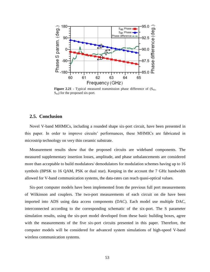
53
2.5. Conclusion
Novel V-band MHMICs, including a rounded shape six-port circuit, have been presented in
this paper. In order to improve circuits’ performances, these MHMICs are fabricated in
microstrip technology on very thin ceramic substrate.
Measurement results show that the proposed circuits are wideband components. The
measured supplementary insertion losses, amplitude, and phase unbalancements are considered
more than acceptable to build modulators/ demodulators for modulation schemes having up to 16
symbols (BPSK to 16 QAM, PSK or dual star). Keeping in the account the 7 GHz bandwidth
allowed for V-band communication systems, the data-rates can reach quasi-optical values.
Six-port computer models have been implemented from the previous full port measurements
of Wilkinson and couplers. The two-port measurements of each circuit on die have been
imported into ADS using data access components (DAC). Each model use multiple DAC,
interconnected according to the corresponding schematic of the six-port. The S parameter
simulation results, using the six-port model developed from these basic building boxes, agree
with the measurements of the five six-port circuits presented in this paper. Therefore, the
computer models will be considered for advanced system simulations of high-speed V-band
wireless communication systems.
Figure 2.21 - Typical measured transmission phase difference of (S61,
S63) for the proposed six-port.

54
In conclusion, this new fabrication run has allowed us to improve the performances of the six-
port circuit in order to be integrated in our future design of an entire millimeter wave front-end
on a 2.54 cm x 2.54 cm thin ceramic substrate. The die will integrate a 2 x 8 elements patch
antenna array, a MMIC Low Noise Amplifier, and a six-port quadrature down-converter.
Acknowledgment
The authors would like to acknowledge the support of the “Centre de Recherche en
Électronique Radiofréquence” (CREER) of Montréal, funded by the “Fonds du recherché du
Quebec –Natures and Technologies” (FRQNT), for the MHMICs fabrication.
References
[1] Federal Communications Commission, “Amendment of Parts 2, 15 and 97 of the
Commission's Rules to Permit Use of Radio Frequencies Above 40 GHz for New Radio
Applications”, FCC 95-499, ET Docket No. 94-124, RM-8308, December 1995.
[2] B. Laemmle, K. Schmalz, J. Borngraeber, J. C. Scheytt, R. Weigel, A. Koelpin, and D.
Kissinger, “A fully integrated 120-GHz six-port receiver front-end in a 130-nm SiGe
BiCMOS technology”, in IEEE Topical Meeting Silicon Monolithic Integrated Circuits in RF
Systems Digest, pp. 129-131, Austin, TX, January 2013.
[3] P. Smulders, “Exploiting the 60 GHz Band for Local Wireless Multimedia Access: prospects
and Future Directions”, IEEE Communications Magazine, no.1, pp. 140-147, January 2002.
[4] A. Koelpin, G. Vinci, B. Laemmle, D. Kissinger, and R. Weigel, “Thesix-port in modern
society,” IEEE Microwave Magazine, vol. 11, no. 7, pp. 35–43, 2010.
[5] T. Eireiner, T. Schnurr, and T. Muller, “Integration of a six-port receiver for mm-wave
communication,” in Proc. IEEE Mediterranean Electrotechnical Conf., pp. 371–376, 2006.
[6] B. Laemmle, K. Schmalz, C. Scheytt, D. Kissinger, and R. Weigel, “A 62 GHz reflectometer
for biomedical sensor readout in SiGe BiCMOS technology”, in IEEE Topical Meeting
Silicon Monolithic Integrated Circuits in RF Systems. Digest., pp. 45-48, Santa Clara, CA,
January 2012.
[7] W. Winkler, “60 GHz Transceiver Circuits in SiGe HBT Technology”, IEEE Compound
Semiconductor Integrated Circuit Symposium Digest, pp. 109-112, November 2005.
55
[8] K. Leong, and T. Itoh, “Advanced and Intelligent RF Front-End Technology”, Wireless
Communication Technology, Conference Proceedings, pp. 190-193, October 2003.
[9] E. Moldovan, S.O. Tatu, S. Affes, Ke Wu, and R. G. Bosisio, “W-band Substrate Integrated
Waveguide Radar Sensor Based on Multi-port Technology”, 4th European Radar
Conference, 2007 European Microwave Week, Conference Proceedings, pp. 174-177,
Munich, October 8 - 12, 2007.
[10] D. Hammou, M. Nedil, N. Kandil, E. Moldovan, S.O. Tatu, “V-band Millimeter-wave
Microstrip to Rectangular Waveguide Transition”, Microwave and Optical Technology
Letters, vol. 55, no.7, pp. 1696–1699, July 2013.
[11] B. Boukari, D. Hammou, E. Moldovan, R. G. Bosisio, Ke Wu, S.O. Tatu, “MHMICs on
Ceramic Substrate for Advanced Millimeter wave Systems”, 2009 IEEE MTT-S
International Microwave Symposium, Boston, Conference Proceedings, pp. 1025-1028, MA,
June 7-12, 2009.
[12] M.Nishimoto, M. Hamai, J. Laskar, Lai, R. ; “Onwafer Calibration Techniques and
Applications at V-band,” IEEE Microwave and Guided Wave Lett., Vol. 4, Issue 11, pp. 370-
372, November 1994.
[13] S.O. Tatu, B. Boukari, E. Moldovan, R. G. Bosisio, Ke Wu, “Millimeter-wave Multi-port
Radar Sensor with Integrated Receiver Front-end for Automotive Applications”, 2012 IEEE
MTT-S International Microwave Symposium, Conference CD, pp.1-4, Montreal, Canada,
June 17-22, 2012.
[14] S.O. Tatu, E. Moldovan, S. Affes, “Multi-Port Front-End and Transceivers for V-Band
Multi-Gigabit/s Communication Systems”, Digital Front-End in Wireless Communications
and Broadcasting Circuits and Signal Processing, ISBN:9781107002135, Chapter DOI:
http://dx.doi.org/10.1017/CBO9780511744839.025, pp. 707-732, Cambridge University
Press, Cambridge, UK, September 2011.
[15] D. Hammou, E. Moldovan, S.O. Tatu, “Novel MHMIC Millimeter Wave Power
Divider/Combiner”, 2011 IEEE Canadian Conference on Electrical and Computer
Engineering (CCECE 2011), Conference proceedings, pp. 280-283, Niagara Falls, Ontario,
May 8-11, 2011.

56
[16] T. Brabetz and V. Fusco, “Six-port receiver front-end MMIC for V-band MBS
applications,” in Proc. 11th Gallium Arsenide Applications (GAAS’03), pp. 97–99, October
2003.
57
CHAPITRE 3 :
PERFORMANCE COMPARISON OF 60 GHZ PRINTED PATCH ANTENNAS WITH DIFFERENT GEOMETRICAL SHAPES USING MINIATURE HYBRID MICROWAVE INTEGRATED CIRCUITS TECHNOLOGY
C. Hannachi, and S.O. Tatu
IET Microwaves Antennas & Propagation, vol. 2016, pp.106-112, October 2016
Résumé : Dans ce chapitre, une étude comparative de différentes formes d'antennes
imprimées a été effectuée. Les formes géométriques considérées sont la forme
rectangulaire, carré, triangulaire, trapézoïdale, circulaire, elliptique et annulaire.
L'objectif principal de cette comparaison est de déterminer la forme géométrique de
l'élément patch, la plus convenable en termes de bande passante, gain, taille, et efficacité.
Cependant, le meilleur élément sera intégré dans un réseau d'antenne comprenant au
minimum 16 éléments, qui sera à son tour implémenté dans le prototype de la frontale
radiofréquence proposée. Il convient également de noter que toutes ces antennes
microrubans ont été conçues en technologie MHMIC sur un substrat en céramique ultra
mince pour permettre un niveau plus élevé d'intégration avec d'autres circuits intégrés
notamment, l'amplificateur faible bruit (LNA), et le circuit six-port tel est le cas dans notre
frontale radiofréquence. Cette étude comparative sera aussi de grande utilité
particulièrement, pour les concepteurs d'antennes puisque elle leur permet de sélectionner
la géométrie d'antenne la plus appropriée lors de la conception des antennes microrubans
opérant à la bande de fréquence de 60 GHz.

58
Abstract
This paper presents a comparative study of several printed antennas having different shapes of
the patch (rectangular, square, triangular, trapezoidal, circular, elliptical, and annular ring),
suitable for 60-GHz wireless applications. All these microstrip patch antennas have been
designed and fabricated on a very thin ceramic substrate to enable a high level of integration with
other integrated circuits including passive circuits (such as power dividers, hybrid couplers,
and passive filters), and active circuits (such as LNA, RF mixers, and frequency multipliers).
In that event, all of those circuits will be incorporated on a single and very small planar substrate
to reduce overall size, and to avoid lossy millimeter-wave connectors. In order to analyze and
compare the performances, Advanced Design System of Keysight Technologies was used for
circuits design and simulation. This comparison is based on the obtained results particularly in
radiation characteristics and inputs return loss, by determining the main associated parameters
such as the bandwidth, VSWR, gain, directivity, efficiency, and cross polarization level. This
comparative study would be very helpful for RF design engineers to select suitable antenna
geometry while designing microstrip patch antenna arrays at 60 GHz millimeter-wave band.
3.1. Introduction
Millimeter-wave microstrip patch antennas are a promising alternative to the future wireless
technologies in various sectors including, military, civil and commercial [1, 2]. This is mainly
due to their low-cost, small size and lightweight, as well as easy fabrication and integration with
any planar fabrication technology, including Miniature Hybrid Microwave Integrated Circuit
(MHMIC) and Monolithic Microwave Integrated Circuit (MMIC) [3-6].
Recently, researchers’ attention has been focused on 60 GHz band with over a 7 GHz of
continuous unlicensed spectrum; this makes the band very desirable for high data rate wireless
applications. Moreover, the short wavelength at 60 GHz enables the design of very compact
elements with very small form factors that could never be achieved in the past on a chip at low
frequencies. Despite these advantages, many factors restrict the use of 60 GHz band for long
distance communication (>2 km) such as, in particular, the oxygen absorption (10-17 dB/km)
and the severe path loss, which is close to 88 dB for 10 m range. However, these adverse effects
can be circumvented by designing high gain, and high directive microstrip patch antennas. For
this purpose, several techniques have been suggested in recent years, for instance, reducing the

59
substrate permittivity (εr) or increasing its thickness (h), introducing parasitic elements, and
using modified shape of the patch [6-8]. Generally, a suitable compromise is desirable between
all these techniques, for example if the substrate thickness (h) is increased beyond 0.1λ0 (0.5
mm); surface-wave propagation takes effect, and the probe inductance increases. On the other
hand, the use of parasitic element increases the overall size of antenna and hence limits their use
as array elements. Other possible approaches are also proposed, among the most relevant, is to
integrate the appropriate single microstrip patch antenna shape into the array structures (2x2,
4x4, and 8x8) to attain a high directional radiation pattern, and high gain (up to 22 dB). On the
one hand, this allows overcoming the gain limitation of the single microstrip patch antenna at 60
GHz millimeter-wave band, which cannot enable high-data rate wireless applications, and
on the other hand, they generate highly directional radiation patterns and narrow beam
widths, which are very desirable for multiple 60 GHz wireless applications. These applications
usually cover a distance between 2 m and 2 Km, and require high gain (10 to 20 dB) as well as
moderate bandwidth (10 to 700 MHz), including particularly, line of sight point-to-point links
(LOS), Giga-bit/s Wireless LAN, broadband fixed wireless access (BFWA), mobile systems
communications, short-range personal communications, and short-range home communications
[9].
In this paper, performance comparison for seven geometric shapes of microstrip patch
antennas designed to operate at 60 GHz band have been carried out in order to investigate the
effect of geometric shape on microstrip patch antennas performances. This comparison deals
with almost all of regular geometric shapes of the microstrip patch at 60 GHz band, including
rectangular, square, triangular, trapezoidal, circular, elliptical, and annular ring. It provides a
more complete view compared to other works in the literature that most of them are focused only
on the more common microstrip antenna shapes such as the rectangular and circular shapes [10-
12]. One of the important considerations in designing the proposed microstrip patch antennas is
the compact size. The latter is the key element to enable a fully integrated 60 GHz transceiver
front-end on a miniature single-chip. For this purpose, a low-loss substrate with a small
thickness and high dielectric constant, compatible with integrated circuit fabrication techniques
is highly required. However, the selected thin film ceramic substrate (h=127 μm, ɛr=9.9) meets
perfectly these requirements, it provides exceptional performances at millimeter wave
60
frequencies up to 90 GHz [13]. In addition, the microstrip lines widths are comparable to the
substrate thickness, which facilitates the design and optimization of the circuits.
3.2. Conventional designs and specifications
Generally, microstrip patch antennas are made of conducting material such as copper, silver
or gold, as was in our case. It is typically composed of a radiating patch on one side of a
dielectric substrate and a ground plane on the other side. The most popular geometries have been
explored in the literature including, the rectangular, triangular, circular and annular ring shapes.
Table 3.1 below shows all these shapes with their characteristic geometric parameters.
As illustrated, for rectangular microstrip patch, W and L are computed for the specific
substrate at the resonance frequency fr [6]. The calculation of length and width is based on the
transmission line method as explained below in (1) and (2), using the effective dielectric constant
εeff and the extension length ∆L in (3) and (4) [11].
The second geometry represents the triangular shaped patch antenna, which has also received
a lot of attention recently [14, 15]. This is due to their small size compared with other shapes
such as the rectangular and circular patch antennas. Regarding the equilateral triangular patch
antenna, at the lowest order resonant frequency fr, the side length a, can given by (5) [16, 17].
For a circular microstrip patch antenna design, a method analysis based on the cavity model
was adopted, by modelling the circular patch, the ground plane and the material between them as
a circular cavity. However, a correction is introduced by using an effective radius reff instead of
the actual radius r, as expressed in (7) and (9) [18-19]. The resonant frequency (fr)110 for the
dominant mode TMz110 is given by (8), where z is taken perpendicular to the patch and the
substrate height is assumed to be very small (h ≪ λ).
The last geometry is the annular ring shaped microstrip antenna. It consists of an inner and
outer radii, designated by a and b, respectively. However, by means of these two parameters, the
separation of resonant modes can be easily controlled. In fact, several analyses confirmed that
the TM21 mode is undoubtedly the best mode because of its good radiation efficiency and its
high performances in circular polarization. Nevertheless, when the annular ring patch works
at this mode, its mean circumferential length is approximately twice the wavelength in effective
permittivity as expressed in (11). Therefore, the operating frequency can be given by (12) [20].
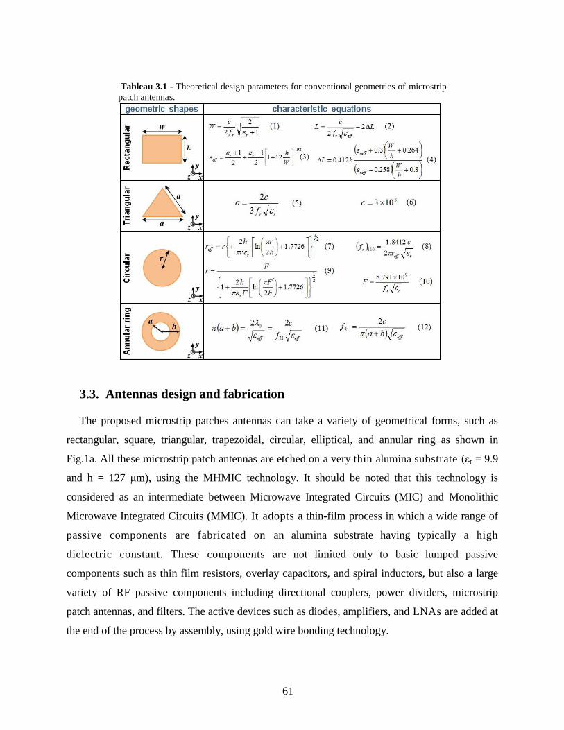
61
3.3. Antennas design and fabrication
The proposed microstrip patches antennas can take a variety of geometrical forms, such as
rectangular, square, triangular, trapezoidal, circular, elliptical, and annular ring as shown in
Fig.1a. All these microstrip patch antennas are etched on a very thin alumina substrate (εr = 9.9
and h = 127 μm), using the MHMIC technology. It should be noted that this technology is
considered as an intermediate between Microwave Integrated Circuits (MIC) and Monolithic
Microwave Integrated Circuits (MMIC). It adopts a thin-film process in which a wide range of
passive components are fabricated on an alumina substrate having typically a high
dielectric constant. These components are not limited only to basic lumped passive
components such as thin film resistors, overlay capacitors, and spiral inductors, but also a large
variety of RF passive components including directional couplers, power dividers, microstrip
patch antennas, and filters. The active devices such as diodes, amplifiers, and LNAs are added at
the end of the process by assembly, using gold wire bonding technology.
Tableau 3.1 - Theoretical design parameters for conventional geometries of microstrip
patch antennas.
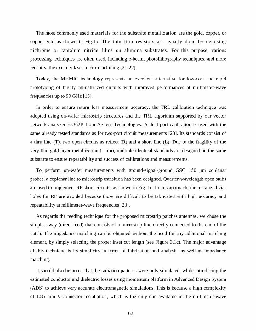
62
The most commonly used materials for the substrate metallization are the gold, copper, or
copper-gold as shown in Fig.1b. The thin film resistors are usually done by deposing
nichrome or tantalum nitride films on alumina substrates. For this purpose, various
processing techniques are often used, including e-beam, photolithography techniques, and more
recently, the excimer laser micro-machining [21-22].
Today, the MHMIC technology represents an excellent alternative for low-cost and rapid
prototyping of highly miniaturized circuits with improved performances at millimeter-wave
frequencies up to 90 GHz [13].
In order to ensure return loss measurement accuracy, the TRL calibration technique was
adopted using on-wafer microstrip structures and the TRL algorithm supported by our vector
network analyzer E8362B from Agilent Technologies. A dual port calibration is used with the
same already tested standards as for two-port circuit measurements [23]. Its standards consist of
a thru line (T), two open circuits as reflect (R) and a short line (L). Due to the fragility of the
very thin gold layer metallization (1 μm), multiple identical standards are designed on the same
substrate to ensure repeatability and success of calibrations and measurements.
To perform on-wafer measurements with ground-signal-ground GSG 150 μm coplanar
probes, a coplanar line to microstrip transition has been designed. Quarter-wavelength open stubs
are used to implement RF short-circuits, as shown in Fig. 1c. In this approach, the metalized via-
holes for RF are avoided because those are difficult to be fabricated with high accuracy and
repeatability at millimeter-wave frequencies [23].
As regards the feeding technique for the proposed microstrip patches antennas, we chose the
simplest way (direct feed) that consists of a microstrip line directly connected to the end of the
patch. The impedance matching can be obtained without the need for any additional matching
element, by simply selecting the proper inset cut length (see Figure 3.1c). The major advantage
of this technique is its simplicity in terms of fabrication and analysis, as well as impedance
matching.
It should also be noted that the radiation patterns were only simulated, while introducing the
estimated conductor and dielectric losses using momentum platform in Advanced Design System
(ADS) to achieve very accurate electromagnetic simulations. This is because a high complexity
of 1.85 mm V-connector installation, which is the only one available in the millimeter-wave
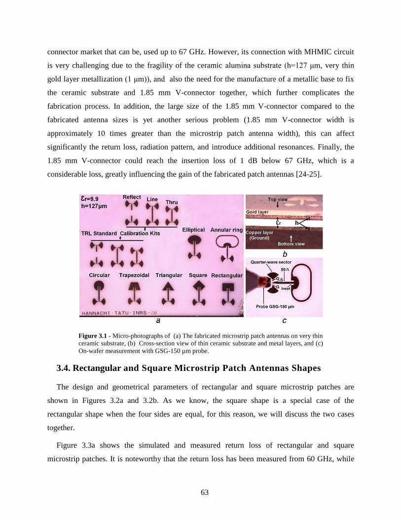
63
connector market that can be, used up to 67 GHz. However, its connection with MHMIC circuit
is very challenging due to the fragility of the ceramic alumina substrate (h=127 μm, very thin
gold layer metallization (1 μm)), and also the need for the manufacture of a metallic base to fix
the ceramic substrate and 1.85 mm V-connector together, which further complicates the
fabrication process. In addition, the large size of the 1.85 mm V-connector compared to the
fabricated antenna sizes is yet another serious problem (1.85 mm V-connector width is
approximately 10 times greater than the microstrip patch antenna width), this can affect
significantly the return loss, radiation pattern, and introduce additional resonances. Finally, the
1.85 mm V-connector could reach the insertion loss of 1 dB below 67 GHz, which is a
considerable loss, greatly influencing the gain of the fabricated patch antennas [24-25].
3.4. Rectangular and Square Microstrip Patch Antennas Shapes
The design and geometrical parameters of rectangular and square microstrip patches are
shown in Figures 3.2a and 3.2b. As we know, the square shape is a special case of the
rectangular shape when the four sides are equal, for this reason, we will discuss the two cases
together.
Figure 3.3a shows the simulated and measured return loss of rectangular and square
microstrip patches. It is noteworthy that the return loss has been measured from 60 GHz, while
Figure 3.1 - Micro-photographs of (a) The fabricated microstrip patch antennas on very thin
ceramic substrate, (b) Cross-section view of thin ceramic substrate and metal layers, and (c)
On-wafer measurement with GSG-150 µm probe.
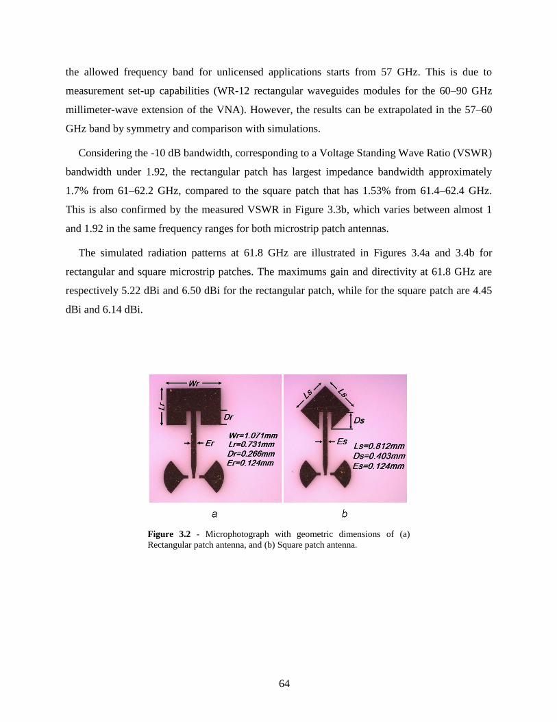
64
the allowed frequency band for unlicensed applications starts from 57 GHz. This is due to
measurement set-up capabilities (WR-12 rectangular waveguides modules for the 60–90 GHz
millimeter-wave extension of the VNA). However, the results can be extrapolated in the 57–60
GHz band by symmetry and comparison with simulations.
Considering the -10 dB bandwidth, corresponding to a Voltage Standing Wave Ratio (VSWR)
bandwidth under 1.92, the rectangular patch has largest impedance bandwidth approximately
1.7% from 61–62.2 GHz, compared to the square patch that has 1.53% from 61.4–62.4 GHz.
This is also confirmed by the measured VSWR in Figure 3.3b, which varies between almost 1
and 1.92 in the same frequency ranges for both microstrip patch antennas.
The simulated radiation patterns at 61.8 GHz are illustrated in Figures 3.4a and 3.4b for
rectangular and square microstrip patches. The maximums gain and directivity at 61.8 GHz are
respectively 5.22 dBi and 6.50 dBi for the rectangular patch, while for the square patch are 4.45
dBi and 6.14 dBi.
Figure 3.2 - Microphotograph with geometric dimensions of (a)
Rectangular patch antenna, and (b) Square patch antenna.

65
3.5. Triangular and Trapezoidal Microstrip Patch Antennas Shapes
Figure 3.5a and 3.5b show, respectively, the geometry of the triangular and trapezoidal
patches. It may be noted that the triangular shape can be obtained from trapezoidal one, when the
smaller base at the top tends towards zero. This brings us to study these two shapes together.
The results of return losses and VSWR are compared over the considered frequency band
with good agreement in Figure 3.6a and 3.6b respectively. These results show that the triangular
Figure 3.3 - Measured and simulated return loss and input VSWR : (a) Measured and simulated
return loss of rectangular and square patch antennas, and (b) Measured VSWR of rectangular and
square patch antennas.
Figure 3.4 - Simulated radiation characteristics at 61.8 GHz of (a) Square patch
antenna and (b) Rectangular patch antenna.

66
patch at -10 dB (VSWR ≈ 1.92) has bandwidth of 0.65 GHz from 61.4 to 62.05 GHz, which
represents the measured 1.92:1 VSWR bandwidth of 0.97% at the resonant frequency (61.7
GHz). For the trapezoidal patch, the measured bandwidth is 1.62% from 61 to 62 GHz (1.92:1
VSWR bandwidth), which is significantly larger than the bandwidth previously obtained by the
triangular patch.
The simulated radiation characteristics for triangular and trapezoidal patches are presented in
Figures 3.7a and 3.7b respectively. The maximums gain and directivity achieved at 61.7 GHz are
successively 4.10 dBi and 5.96 dBi for the triangular patch, whereas for the trapezoidal patch are
4.30 dBi and 6.14 dBi.
Measured bandwidth is 1.62% from 61 to 62 GHz (1.92:1 VSWR bandwidth), which is
significantly larger than the bandwidth previously obtained by the triangular patch.
The simulated radiation characteristics for triangular and trapezoidal patches are presented in
Figure 3.7a and 3.7b respectively. The maximums gain and directivity achieved at 61.7 GHz are
successively 4.10 dBi and 5.96 dBi for the triangular patch, whereas for the trapezoidal patch are
4.30 dBi and 6.14 dBi.
Figure 3.5 - Micro-photograph with geometric dimensions of (a)
Triangular patch antenna and (b) Trapezoidal patch antenna.

67
3.6. Circular and Elliptical Microstrip Patch Antennas Shapes
Figures 3.8a and 3.8b show the geometry of the proposed circular and elliptical microstrip
patch antennas with detailed dimensions. As can be seen, the circular shape can be obtained from
the elliptical shape when the smaller radius R2 and the largest radius R1 are equal. For that
reason, we have analyzed the two microstrip patches together.
The simulated and measured results of return loss, as well as the measured VSWR are shown
in Figures 3.9a and 3.9b over the same frequency range, 60 to 64 GHz, taking into account the
Figure 3.6 - Measured and simulated return loss, and input VSWR : (a) Measured and simulated
return loss of triangular and trapezoidal patch antennas, (b) Measured VSWR of triangular and
trapezoidal patch antennas.
Figure 3.7 - Simulated radiation characteristics at 61.7 GHz of (a) Triangular
patch antenna and, (b) Trapezoidal patch antenna

68
unlicensed V-band and our measurement capabilities. In terms of return losses, good agreement
between simulated and measured results is obtained for both circular and elliptical microstrip
patches. However, we can observe a resonant frequency shift of 1.5% between simulated and
measured return loss for each microstrip patch antenna. This frequency shift is also clearly
observed in the measured VSWR in Figure 3.9b. Generally, such shift in the frequency can be
caused by the fabrication tolerances, higher dielectric constant substrate and the reflections
due to the time effect to remove GSG 150 µm coplanar probes. The measured impedance
bandwidths (1.92:1 VSWR bandwidths) are 1.65% (60.1–61.1 GHz) and 1.79 % (60.9–62 GHz),
respectively, for the circular and elliptical microstrip patches. It is very clear from these two
figures that the elliptical microstrip patch offers higher bandwidth compared to the circular
microstrip patch.
The simulated radiation characteristics of both circular and elliptical microstrip patches at 61
GHz are shown in Figures 3.10a and 3.10b. As these figures show, the maximum gain and
directivity for both are respectively 4.60 dBi and 6.22 dBi for the circular patch, while for the
elliptical patch are 4.44 dBi and 6.18 dBi.
Figure 3.8 - Microphotograph with geometric dimensions of, (a)
Circular patch antenna and, (b) Elliptical patch antenna.
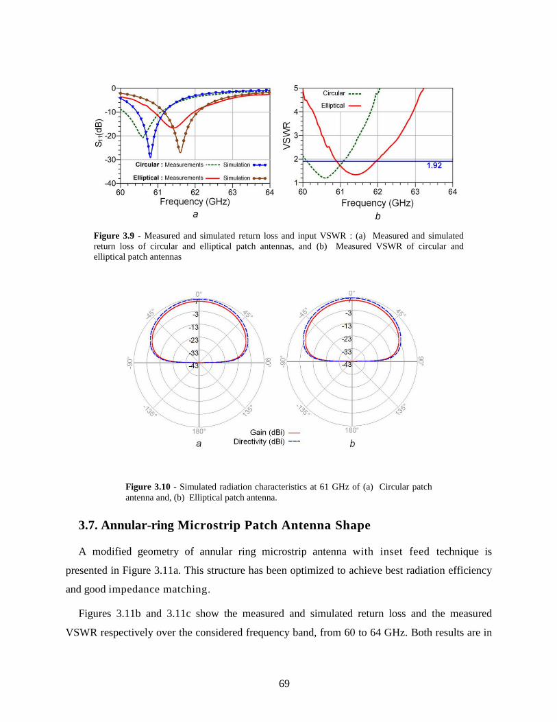
69
3.7. Annular-ring Microstrip Patch Antenna Shape
A modified geometry of annular ring microstrip antenna with inset feed technique is
presented in Figure 3.11a. This structure has been optimized to achieve best radiation efficiency
and good impedance matching.
Figures 3.11b and 3.11c show the measured and simulated return loss and the measured
VSWR respectively over the considered frequency band, from 60 to 64 GHz. Both results are in
Figure 3.9 - Measured and simulated return loss and input VSWR : (a) Measured and simulated
return loss of circular and elliptical patch antennas, and (b) Measured VSWR of circular and
elliptical patch antennas
Figure 3.10 - Simulated radiation characteristics at 61 GHz of (a) Circular patch
antenna and, (b) Elliptical patch antenna.
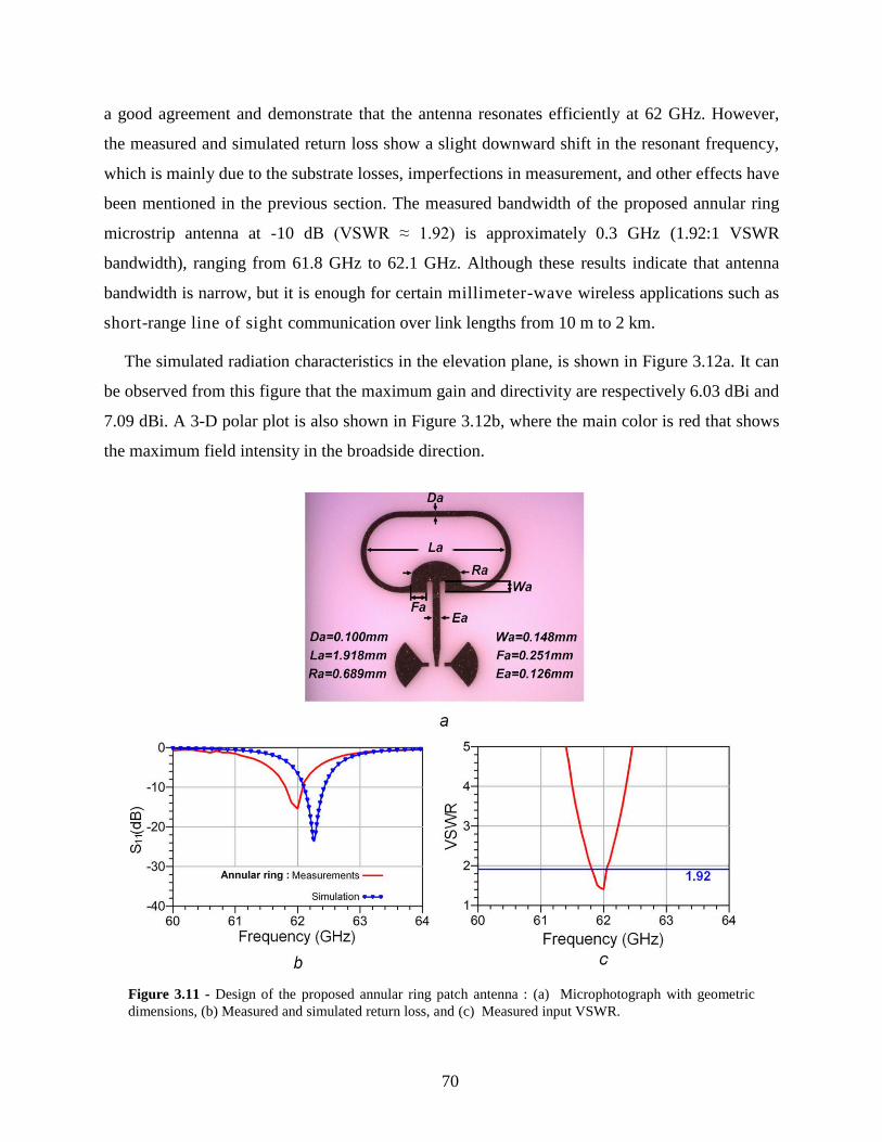
70
a good agreement and demonstrate that the antenna resonates efficiently at 62 GHz. However,
the measured and simulated return loss show a slight downward shift in the resonant frequency,
which is mainly due to the substrate losses, imperfections in measurement, and other effects have
been mentioned in the previous section. The measured bandwidth of the proposed annular ring
microstrip antenna at -10 dB (VSWR ≈ 1.92) is approximately 0.3 GHz (1.92:1 VSWR
bandwidth), ranging from 61.8 GHz to 62.1 GHz. Although these results indicate that antenna
bandwidth is narrow, but it is enough for certain millimeter-wave wireless applications such as
short-range line of sight communication over link lengths from 10 m to 2 km.
The simulated radiation characteristics in the elevation plane, is shown in Figure 3.12a. It can
be observed from this figure that the maximum gain and directivity are respectively 6.03 dBi and
7.09 dBi. A 3-D polar plot is also shown in Figure 3.12b, where the main color is red that shows
the maximum field intensity in the broadside direction.
Figure 3.11 - Design of the proposed annular ring patch antenna : (a) Microphotograph with geometric
dimensions, (b) Measured and simulated return loss, and (c) Measured input VSWR.
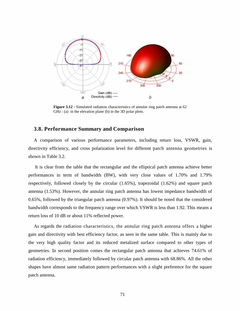
71
3.8. Performance Summary and Comparison
A comparison of various performance parameters, including return loss, VSWR, gain,
directivity efficiency, and cross polarization level for different patch antenna geometries is
shown in Table 3.2.
It is clear from the table that the rectangular and the elliptical patch antenna achieve better
performances in term of bandwidth (BW), with very close values of 1.70% and 1.79%
respectively, followed closely by the circular (1.65%), trapezoidal (1.62%) and square patch
antenna (1.53%). However, the annular ring patch antenna has lowest impedance bandwidth of
0.65%, followed by the triangular patch antenna (0.97%). It should be noted that the considered
bandwidth corresponds to the frequency range over which VSWR is less than 1.92. This means a
return loss of 10 dB or about 11% reflected power.
As regards the radiation characteristics, the annular ring patch antenna offers a higher
gain and directivity with best efficiency factor, as seen in the same table. This is mainly due to
the very high quality factor and its reduced metalized surface compared to other types of
geometries. In second position comes the rectangular patch antenna that achieves 74.61% of
radiation efficiency, immediately followed by circular patch antenna with 68.86%. All the other
shapes have almost same radiation pattern performances with a slight preference for the square
patch antenna.
Figure 3.12 - Simulated radiation characteristics of annular ring patch antenna at 62
GHz : (a) in the elevation plane (b) in the 3D polar plots.

72
In terms of cross polarization level (XPL), the proposed microstrip patch antennas exhibit
very low cross polarization levels, better than -40 dB at broadside for all microstrip patch
antenna shapes, except for the annular ring shaped microstrip antenna, which is better than -38
dB. In overall terms, these results are excellent for all proposed microstrip patch antennas and
meet perfectly the cross polarization requirements at 60 GHz millimeter-waves band. They are
also very important, especially for microstrip antenna arrays, because a poor cross polarization
level (XPL) degrades significantly the performance of communication systems,
predominantly by a gain reduction and a very bad establishment of the polarization state.
This comparison clearly proves that the rectangular patch presents the best possible
compromise in terms of performance, which has at the same time larger bandwidth, high gain,
high directivity, better radiation efficiency, and low cross polarization level. However, its large
dimensions compared to other geometries at the same operating frequency constitute its major
weak point.
3.9. Conclusion
In this paper, seven different geometric shapes of microstrip patch antennas suited for use at
60 GHz millimeter-wave band were fabricated, characterized and investigated. To understand the
impact of geometric shapes on the antenna performances, a comprehensive comparative study
between the various fabricated patch antennas has been done.
Tableau 3.2 : Comparison Table of the performances between 7 shapes of fabricated microstrip patch antennas.
73
From this analysis, it can be concluded that the geometrical shape of the patch has a
significant impact on the bandwidth with variation of 0.8 GHz between a larger (elliptical) and a
narrower (annular ring) bandwidth. Moreover, the radiation characteristics were also affected by
the patch geometry; there was 1.1 dBi of variation between maximum and minimum gain
reached respectively by the annular ring and triangular patch. Similarly, for the radiation
efficiency that has a difference of more than 12% between the maximum (annular ring) and
minimum efficiency (triangular patch). As regards the cross polarization level, the obtained
results show that the microstrip antenna shapes does not have a potential impact on cross
polarization level, except for the case of annular ring microstrip antenna that indicates -38.5 dB
(3.5 dB more than the lowest value of -42 dB (triangular patch)). However, a tradeoff which
satisfied both, antenna geometry and antenna performances must be achieved.
In this context, the rectangular patch is by far the best appropriated and the most commonly
used configuration at lower or millimeter-waves frequencies. It is very easy to analyze using
both the transmission-line and cavity models, which are most accurate especially, for thin
substrates such as the case of our study.
Acknowledgments
The authors would like to acknowledge the Natural Sciences and Engineering Research
Council of Canada (NSERC), for the generous research support, and the “Centre de Recherche
en Électronique Radiofréquence” (CREER) of Montréal, funded by the “Fonds de recherche du
Quebec–Natures and technologies” (FRQNT), for the MHMICs fabrication.
References
[1] Pozar, D.M.: ‘Considerations for millimeter wave printed antennas’, IEEE Trans. Antennas
Propag., 1983, 31, (5), pp. 740- 747
[2] Lee, K., Tong, K.: ‘Microstrip patch antennas – basic characteristics and some recent
advances’. Proc. of the IEEE, 2012, 100, (7), pp. 2169–2180
[3] Kim, D.Y., Mun, J.K., and Kim, C.S.: ‘Design of antenna with broadband and high gain at
millimeter wave band’, Electron. Lett., 2012, 48, (22), pp. 1382–1383

74
[4] Rajab, K.Z., Mittra, R., and Lanagan, M.T.: ‘Size reduction of microstrip patch antennas with
left-handed transmission line loading’, IET Microw. Antennas Propag., 2007, 1, (1), pp. 39–
44
[5] Lee, K.F., Luk, K.M.: ‘Microstrip patch antennas’ (Imperial College Press, London, UK,
2011)
[6] G. Kumar and K.P. Ray.: ‘Broadband Microstrip Antennas’ (Artech House, Boston, USA,
2003)
[7] Dejean, Li, R., Tentzeris, G., and Laskar, J.: ‘Development and analysis of a folded shorted-
patch antenna with reduced size’, IEEE Trans. Antennas Propag., 2004, 52, (2), pp. 555–562
[8] Hannachi, C., Tatu, S.O.: ‘A New Compact V-band Six-port Down-Converter Receiver for
High Data Rate Wireless Applications’. IEEE Topical Conference on Wireless Sensors and
Sensor Networks (WiSNet), San Diego, CA, January 2015, pp. 26–28
[9] Ofcom Contract 410000258., ‘Radio Systems at 60GHz and Above’ (Rutherford Appleton
Laboratory, 2006), pp. 1-194
[10] Agarwal, S., Pathak, N. P., Singh, D.: ‘Performance comparison of microstrip patch
antenna for 94 GHz imaging applications’. 7th IEEE International Conference on Industrial
and Information Systems (ICIIS), Chennai, India, Aug. 2012, pp.1-4
[11] Yahya, S., Olaimat, M.M., Abdel-Razeq, S.N.: ‘Comparison between rectangular and
triangular patch antenna arrays’, Appl. Phys. Res., 2012, 4, p. 1-5
[12] Mathur, V., Gupta, M.: ‘Comparison of performance characteristics of rectangular,
square and hexagonal microstrip patch antennas’. 3rd International Conference on
Reliability, Infocom Technologies and Optimization (ICRITO), Noida, India, October 2014,
pp. 8-10
[13] Moldovan, E., Tatu, S.O.: ‘Design and Characterization of Novel W-band Wide-band
Couplers and Six-port Circuit’. European Microwave Week, Conference proceedings, Paris,
France, September 2015, pp. 279-282
[14] Garg, R., Long, S.A.: ‘An improved formula for the resonant frequency of triangular
microstrip patch antennas’, IEEE Trans. Antennas Propag., 1988, 36, (4), pp. 570
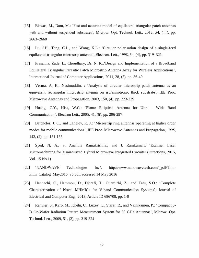
75
[15] Biswas, M., Dam, M.: ‘Fast and accurate model of equilateral triangular patch antennas
with and without suspended substrates’, Microw. Opt. Technol. Lett., 2012, 54, (11), pp.
2663–2668
[16] Lu, J.H., Tang, C.L., and Wong, K.L.: ‘Circular polarisation design of a single-feed
equilateral-triangular microstrip antenna’, Electron. Lett., 1998, 34, (4), pp. 319–321
[17] Prasanna, Zade, L., Choudhary, Dr. N. K.:‘Design and Implementation of a Broadband
Equilateral Triangular Parasitic Patch Microstrip Antenna Array for Wireless Applications’,
International Journal of Computer Applications, 2011, 28, (7), pp. 36-40
[18] Verma, A. K., Nasimuddin. : ‘Analysis of circular microstrip patch antenna as an
equivalent rectangular microstrip antenna on iso/anisotropic thick substrate’, IEE Proc.
Microwave Antennas and Propagation, 2003, 150, (4), pp. 223-229
[19] Huang, C.Y., Hisa, W.C.: ‘Planar Elliptical Antenna for Ultra - Wide Band
Communication’, Electron Lett., 2005, 41, (6), pp. 296-297
[20] Batchelor, J. C., and Langley, R. J.: ‘Microstrip ring antennas operating at higher order
modes for mobile communications’, IEE Proc. Microwave Antennas and Propagation, 1995,
142, (2), pp. 151-155
[21] Syed, N. A., S. Anantha Ramakrishna., and J. Ramkumar.: ‘Excimer Laser
Micromachining for Miniaturized Hybrid Microwave Integrated Circuits’ (Directions, 2015,
Vol. 15 No.1)
[22] ‘NANOWAVE Technologies Inc’, http://www.nanowavetech.com/_pdf/Thin-
Film_Catalog_May2015_v5.pdf, accessed 14 May 2016
[23] Hannachi, C., Hammou, D., Djerafi, T., Ouardirhi, Z., and Tatu, S.O.: ‘Complete
Characterization of Novel MHMICs for V-band Communication Systems’, Journal of
Electrical and Computer Eng., 2013, Article ID 686708, pp. 1-9
[24] Ranvier, S., Kyro, M., Icheln, C., Luxey, C., Staraj, R., and Vainikainen, P.: ‘Compact 3-
D On-Wafer Radiation Pattern Measurement System for 60 GHz Antennas’, Microw. Opt.
Technol. Lett., 2009, 51, (2), pp. 319-324

76
[25] Hrobak, M.: ‘Critical mm-Wave Components for Synthetic Automatic Test Systems’
(Springer Vieweg, Berlin, Germany, 2015)

77
CHAPITRE 4 :
A COMPACT V-BAND PLANAR GAP-COUPLED 4X1 ANTENNA ARRAY: IMPROVED DESIGN AND ANALYSIS
C. Hannachi, and S.O. Tatu
Acess IEEE, vol. 2017, pp.1-7, March 2017
Résumé : Ce chapitre présente une nouvelle structure de réseau d'antenne microrubans à 4
éléments en utilisant la technique de couplage par proximité en ondes millimétriques,
particulièrement dans la bande de 57 à 65 GHz. Afin de répondre à la problématique de
réduction de la taille liée à ce genre de technique et de faciliter l'intégration du réseau
conçu avec d'autres composants passifs ou actifs, le réseau d'antennes proposé a été conçu
en adoptant un procédé de fabrication MHMIC (Miniature Hybrid Microwave Integrated
Circuits) sur un substrat en céramique ultra mince, ayant une permittivité relative de εr =
9,9 et une épaisseur de h = 127 μm. La structure proposée est basée sur une forme
améliorée d'un élément patch ayant des bords rayonnants incurvés. Pour une analyse plus
approfondie, les performances de ce dernier en terme de largeur de bande, ont été évaluée
et comparées avec la structure classique d'une antenne patch rectangulaire élémentaire,
adoptant la même technique de couplage par proximité.
Le réseau d'antenne microrubans à 4 éléments proposé montrent des performances
améliorées, au niveau de la largeur de bande (7%), et un gain d'environ 10,7 dB tout en
maintenant une taille réduite (5,2 mm x 9,5 mm). Ces excellentes performances font de lui
un candidat approprié pour les futures frontales radiofréquences intégrées opérant en
ondes millimétriques ; Il peut être relié directement à divers circuits MHMIC passifs, ou à
des dispositifs actifs par l'intermédiaire de la technologie de liaison par fil, sur un substrat
d'alumine ultra mince standard.

78
Abstract
In this paper, a broadband 60-GHz millimeter-wave 4x1 microstrip patch antenna array using
gap-coupled technique is presented and analyzed. In order to meet the challenging requirement
of reduced size related to this kind of technique, and facilitate the integration with other
integrated passive or active devices, the proposed antenna array has been designed on thin
ceramic substrate (εr = 9.9 , h = 127 μm), using an MHMIC (Miniature Hybrid Microwave
Integrated Circuits) fabrication process. The proposed structure is based on an improved shape of
a gap-coupled patch element with curved radiating edges. For further analysis, the performances
of the latter in term of impedance bandwidth, gain and radiation efficiency were investigated and
compared with a conventional structure of rectangular gap-coupled patch antenna. The obtained
results clearly show that the proposed gap-coupled array structure provides an improved
bandwidth (7 %), and an enhanced gain (10.7 dB), while maintaining a reduced size (5.2 mm x
9.5 mm). All these benefits make it an attractive candidate for the future integrated millimeter-
wave RF front-end circuits; it can, however, be connected directly to various MHMIC passive
circuits, or active devices through using the wire bonding technology, on a standard thin-film
alumina substrate.
4.1. Introduction
Recently, printed antennas for millimeter-wave applications has become an increasingly
important topic given the attractive features such as low profile, light weight, low manufacturing
cost, and ease of fabrication and integration with Miniature Hybrid Microwave Integrated
Circuits (MHMICs) or Microwave Monolithic Integrated Circuits (MMICs). They have become
key components to many diverse commercial, industrial, and military applications including
aircraft, spacecraft, satellite, missiles, cars and even handheld mobile telephones [1]. Despite its
many advantages, the general design of microstrip patch antenna usually suffers from its intrinsic
narrow bandwidth, which is of the order of a few percent (2% - 5%). This characteristic
constitutes a real limitation in most of the wireless communication systems that are increasingly
designed for supporting a large number of users and providing high data-rate information [2].
In order to overcome this constraint, various techniques were adopted to increase the
bandwidth of microstrip patch antennas, such as the slot-loading technique, the multilayered
technique, the stacked multilayered technique and by using modified or partial ground [3]-[10].

79
However, their implementation in practice further complicates the fabrication process, and may
pose a difficulty in terms of integration with the existing planar fabrication processes. Many
other approaches related to the substrate material choices have also been proposed for enhancing
the bandwidth, for instance, by increasing the electrical thickness of the substrate, or by reducing
the dielectric constant. Indeed, the increase in substrate thickness significantly degrades the
antenna efficiency, especially at millimeter-wave frequencies due to surface wave effects; on the
other hand, there are practical limitations in decreasing the dielectric constant [2].
Gap-coupled multiple resonators technique used in microstrip antenna structures, is among
the most promising techniques, and the simple solutions that have been proven to significantly
increase operational bandwidth and antenna gain. They have been subject to numerous
researches over the past years, but, nonetheless, the vast majority of them have brought more
interest for low-frequency antenna structures [11]-[20]. Therefore, they do not consider the same
issues as in millimeter-wave frequencies, particularly at 60 GHz band. In fact, at this frequency
band, the surface wave propagations and the high mutual coupling between adjacent elements
have a severe impact on the antenna radiation performance. Moreover, the signals are
supplementary attenuated (10-17 dB/km) due to oxygen absorption, in addition to inherent very
high path loss due to the operating frequency. This restricts the use of 60 GHz band for long
distance communication (> 2 km), and hence makes it entirely suitable for short-range wireless
communications (several meters for low power to max 1 km for backhaul solutions) [21]-[23].
The frequency reuse is, therefore, one of the main advantages. Nevertheless, these drawbacks
can be limited by designing the antennas having a high efficiency, high gain, an acceptable
bandwidth, and readily expandable to the compact array configurations.
In this paper, a compact broadband 4x1 millimeter-wave microstrip patch antenna array using
gap-coupled technique is designed, fabricated, and analyzed. The proposed structure is based on
gap-coupled microstrip patch elements having curved radiating edges. For performance
comparison, an equivalent rectangular gap-coupled patch antenna was also designed as a
reference antenna. In order to enable a compact size that usually constitutes a major problem in
this kind of technique, an MHMIC fabrication process, and a thin ceramic substrate with high
dielectric constant (εr = 9.9, h = 127 μm) have been employed. Finally, to investigate the
coupling effect of the gap on the proposed gap-coupled structure, parametric studies were
conducted to enable a gap width and input impedance matching optimization.

80
4.2. Antenna designs, fabrication, and measurement
In order to point out the usefulness of the proposed gap-coupled structure in the optimization
of the coupling between the driven patch and parasitic element, a conventional rectangular
microstrip patch antenna is used as reference antenna for performance comparison. Therefore, a
consistent comparison between single rectangular patch (SRP) and single modified patch (SMP)
antenna, as well as between their associated gap-coupled configurations is performed. For that
purpose, Advanced Design System (ADS) software of Keysight Technologies is used for circuit
design, simulation, and performance analysis. As a manufacturing technique, a standard MHMIC
fabrication process on thin ceramic substrate has been adopted. The latter provides several
interesting features, including miniature circuits, low costs, as well as high level of integration
and the use of high precision thin film resistors, fabricated with microstrip line, such as in the
case of our fabricated gap-coupled array prototype.
The geometrical configurations of the optimized single modified patch (SMP) and its
equivalent single rectangular patch (SRP) antenna are shown in Figure 4.1. Their physical
parameters are: W=2R=1.071, L= 0.731, W0= 0.708, L1= 0.266, L2= 0.307, d= 0.411, d1= 0.231,
d2= 0.180, e=e1= 0.061, e2= 0.093, W1=W2=0.127, D= 0.660, f= 0.058, f1= 0.078, E= 0.152, all
units being millimeters.
Figure 4.1 - Single modified patch antenna and its equivalent
rectangular patch in (a) Photograph of the fabricated prototypes with
the geometrical parameters of the single rectangular patch antenna,
and single modified patch antenna in (b), and (c) respectively.
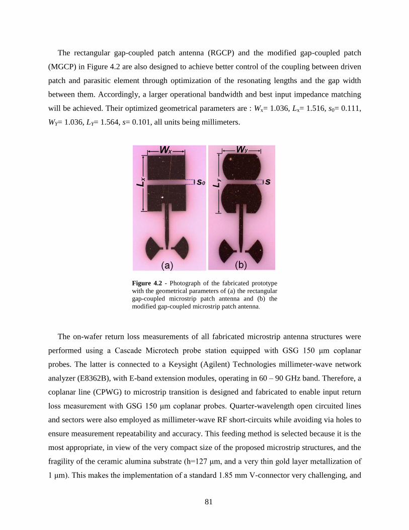
81
The rectangular gap-coupled patch antenna (RGCP) and the modified gap-coupled patch
(MGCP) in Figure 4.2 are also designed to achieve better control of the coupling between driven
patch and parasitic element through optimization of the resonating lengths and the gap width
between them. Accordingly, a larger operational bandwidth and best input impedance matching
will be achieved. Their optimized geometrical parameters are : Wx= 1.036, Lx= 1.516, s0= 0.111,
WY= 1.036, LY= 1.564, s= 0.101, all units being millimeters.
The on-wafer return loss measurements of all fabricated microstrip antenna structures were
performed using a Cascade Microtech probe station equipped with GSG 150 μm coplanar
probes. The latter is connected to a Keysight (Agilent) Technologies millimeter-wave network
analyzer (E8362B), with E-band extension modules, operating in 60 – 90 GHz band. Therefore, a
coplanar line (CPWG) to microstrip transition is designed and fabricated to enable input return
loss measurement with GSG 150 μm coplanar probes. Quarter-wavelength open circuited lines
and sectors were also employed as millimeter-wave RF short-circuits while avoiding via holes to
ensure measurement repeatability and accuracy. This feeding method is selected because it is the
most appropriate, in view of the very compact size of the proposed microstrip structures, and the
fragility of the ceramic alumina substrate (h=127 μm, and a very thin gold layer metallization of
1 μm). This makes the implementation of a standard 1.85 mm V-connector very challenging, and
Figure 4.2 - Photograph of the fabricated prototype
with the geometrical parameters of (a) the rectangular
gap-coupled microstrip patch antenna and (b) the
modified gap-coupled microstrip patch antenna.
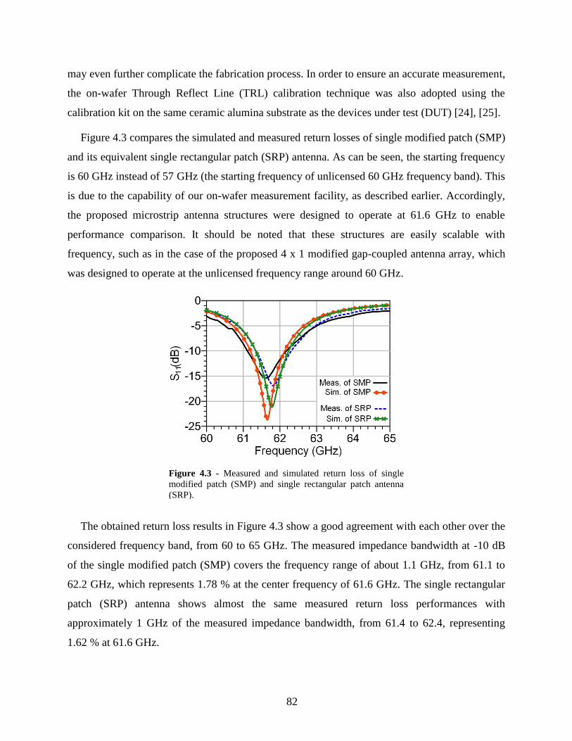
82
may even further complicate the fabrication process. In order to ensure an accurate measurement,
the on-wafer Through Reflect Line (TRL) calibration technique was also adopted using the
calibration kit on the same ceramic alumina substrate as the devices under test (DUT) [24], [25].
Figure 4.3 compares the simulated and measured return losses of single modified patch (SMP)
and its equivalent single rectangular patch (SRP) antenna. As can be seen, the starting frequency
is 60 GHz instead of 57 GHz (the starting frequency of unlicensed 60 GHz frequency band). This
is due to the capability of our on-wafer measurement facility, as described earlier. Accordingly,
the proposed microstrip antenna structures were designed to operate at 61.6 GHz to enable
performance comparison. It should be noted that these structures are easily scalable with
frequency, such as in the case of the proposed 4 x 1 modified gap-coupled antenna array, which
was designed to operate at the unlicensed frequency range around 60 GHz.
The obtained return loss results in Figure 4.3 show a good agreement with each other over the
considered frequency band, from 60 to 65 GHz. The measured impedance bandwidth at -10 dB
of the single modified patch (SMP) covers the frequency range of about 1.1 GHz, from 61.1 to
62.2 GHz, which represents 1.78 % at the center frequency of 61.6 GHz. The single rectangular
patch (SRP) antenna shows almost the same measured return loss performances with
approximately 1 GHz of the measured impedance bandwidth, from 61.4 to 62.4, representing
1.62 % at 61.6 GHz.
Figure 4.3 - Measured and simulated return loss of single
modified patch (SMP) and single rectangular patch antenna
(SRP).
83
Figure 4.4 shows the measured return loss comparing with the simulated one over the
investigated frequency band (60 to 65 GHz) for the modified gap-coupled patch (MGCP) and the
rectangular gap-coupled patch antenna (RGCP). As can be seen from Figure 4.4, the comparison
of measured and simulated insertion loss showed very good agreement. The modified gap-
coupled patch (MGCP) resonates efficiently at 61.6 GHz and 63.9 GHz, with a measured
impedance bandwidth of 3.7 GHz, from 60.7 to 64.4 GHz, representing, 5.92 % at the center
frequency of 62.5 GHz.
The rectangular gap-coupled patch antenna (RGCP), can reach a measured impedance
bandwidth of 2.6 GHz (4.16 % at the center frequency of 62.5 GHz), from 60.4 to 63 GHz,
which is clearly 1.1 GHz less than the measured bandwidth obtained previously in modified gap-
coupled patch (MGCP).
However, a slight resonant frequency shift between simulated and measured return loss is
observed for both structures, which is mainly due to the, tolerances of the dielectric constant and
thickness of the ceramic substrate, substrate losses, and fabrication tolerances.
In order to investigate the impact of the proposed single and gap-coupled configurations in
Figure 4.1(c) and Figure 4.2(b) on the gain and efficiency, a comparative study at the operating
frequency bands (-10 dB return loss bandwidth) is carried out. For that purpose, the single
rectangular patch antenna (SRP) and rectangular gap-coupled patch antenna (RGCP) in Figure
4.1(b) and Figure 4.2(a) are considered as reference antennas for performance comparison. In
Figure 4.4 - Measured and simulated return loss of the modified gap-
coupled patch (MGCP) and the rectangular gap-coupled patch
antenna (RGCP).
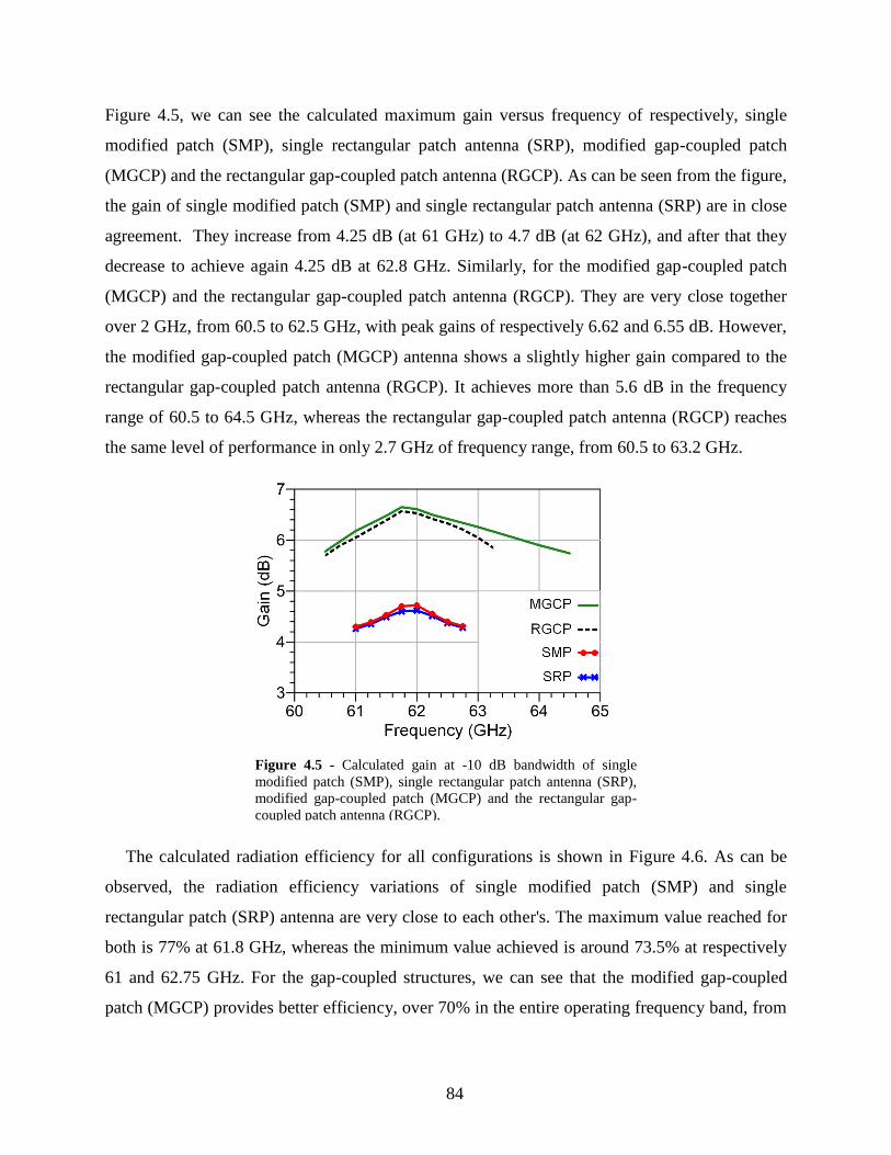
84
Figure 4.5, we can see the calculated maximum gain versus frequency of respectively, single
modified patch (SMP), single rectangular patch antenna (SRP), modified gap-coupled patch
(MGCP) and the rectangular gap-coupled patch antenna (RGCP). As can be seen from the figure,
the gain of single modified patch (SMP) and single rectangular patch antenna (SRP) are in close
agreement. They increase from 4.25 dB (at 61 GHz) to 4.7 dB (at 62 GHz), and after that they
decrease to achieve again 4.25 dB at 62.8 GHz. Similarly, for the modified gap-coupled patch
(MGCP) and the rectangular gap-coupled patch antenna (RGCP). They are very close together
over 2 GHz, from 60.5 to 62.5 GHz, with peak gains of respectively 6.62 and 6.55 dB. However,
the modified gap-coupled patch (MGCP) antenna shows a slightly higher gain compared to the
rectangular gap-coupled patch antenna (RGCP). It achieves more than 5.6 dB in the frequency
range of 60.5 to 64.5 GHz, whereas the rectangular gap-coupled patch antenna (RGCP) reaches
the same level of performance in only 2.7 GHz of frequency range, from 60.5 to 63.2 GHz.
The calculated radiation efficiency for all configurations is shown in Figure 4.6. As can be
observed, the radiation efficiency variations of single modified patch (SMP) and single
rectangular patch (SRP) antenna are very close to each other's. The maximum value reached for
both is 77% at 61.8 GHz, whereas the minimum value achieved is around 73.5% at respectively
61 and 62.75 GHz. For the gap-coupled structures, we can see that the modified gap-coupled
patch (MGCP) provides better efficiency, over 70% in the entire operating frequency band, from
Figure 4.5 - Calculated gain at -10 dB bandwidth of single
modified patch (SMP), single rectangular patch antenna (SRP),
modified gap-coupled patch (MGCP) and the rectangular gap-
coupled patch antenna (RGCP).

85
60.5 to 64.5 GHz. However, the same performance is obtained for the rectangular gap-coupled
patch antenna (RGCP), in only 2.7 GHz of operating frequency band, from 60.5 to 63.2 GHz.
4.3. Theoretical analysis
The proposed modified gap-coupled patch (MGCP) structure can be analyzed for the two
modes, commonly known as even and odd. The theory of such structures has recently been well
investigated in the literature [11], [26]. However, this structure can be analyzed by adopting the
theory of coupled microstrip lines and coupled microstrip antenna. In this analysis, the total
capacitance of the coupled structure is taken as parallel plate capacitance (Cp) and two fringing
capacitances (Cf, Cf`) for both even and odd mode. It should be noted that the additional fringing
capacitance at the adjacent edge of the patches is in fact the result of the additional parasitic
element in the proposed gap-coupled microstrip patch structure. Figure 4.7 shows in detail all
those capacitances for both modes, even and odd respectively.
The values of these capacitances can be expressed in terms of even and odd mode parameters
for propagation, as illustrated in Table 4.1 [11], [26].
From the table, it is noted that the expressions for the capacitances cited earlier including Cp,
Cf, and Cf ` are given respectively in (1), (2), and (3). We can also distinguish two other
Figure 4.6 - Calculated efficiency at -10 dB bandwidth of single
modified patch (SMP), single rectangular patch antenna (SRP),
modified gap-coupled patch (MGCP) and the rectangular gap-
coupled patch antenna (RGCP).

86
capacitances that characterize the coupling effect between the fed patch and the parasitic patch in
odd mode. The first one is the dielectric coupling capacitance Cgd, which represents the
capacitance value due to the electric flux in the dielectric area, where its value is calculated in
(5). While for the second one, is the air coupling capacitance Cga, which describes the gap
capacitance in air. Its value can be obtained from (6), where K (k) and K (k`) designate the
elliptic function and its complement (7).
From the table, it is noted that the expressions for the capacitances cited earlier including Cp,
Cf, and Cf `are given respectively in (1), (2), and (3). We can also distinguish two other
capacitances that characterize the coupling effect between the fed patch and the parasitic patch in
odd mode. The first one is the dielectric coupling capacitance Cgd, which represents the
capacitance value due to the electric flux in the dielectric area, where its value is calculated in
(5). While for the second one, is the air coupling capacitance Cga, which describes the gap
capacitance in air. Its value can be obtained from (6), where K (k) and K (k`) designate the elliptic
function and its complement (7).
In this analysis, particular attention is paid to the coupling effect between the driven element
and a parasitic one. However, according to the Table 4.1, this effect can be assessed
quantitatively by estimating the values of the dielectric coupling capacitance Cgd and the air
Tableau 4.1 - Even and Odd mode Capacitances Equations.
Figure 4.7 - Even and odd mode capacitances of the
proposed gap-coupled microstrip patch antenna
structure.

87
coupling capacitance Cga, for different normalized gap distances s/h. The obtained results for
those capacitances with the employed alumina substrate are shown in Figure 4.8.
It is noteworthy that the normalized gap width used to obtain the results is increased every
step by 0.1 (one-tenth of the substrate height h), reaching a maximum value of 1, which
corresponds to an overall increase of one time the substrate height h (s=h). In view of these
considerations, it can be seen that as the gap width increases, the coupling effect decreases for
both capacitances, Cgd and Cga. The dielectric coupling capacitance Cgd and the air coupling
capacitance Cga have reached their maximum values at respectively 0.162 pF/mm and 0.0125
pF/mm, for s/h=0.1. While the minimum values reached by these capacitances are respectively
0.072 pF/mm and 0.0069 pF/mm, for s/h=1. These results clearly demonstrate that the variations
of the dielectric coupling capacitance Cgd are approximately ten times higher than the variations
of the air coupling capacitance Cga. This may be explained by the high relative dielectric
constant (εr = 9.9) and low thickness (h = 127 μm) of the used alumina substrate.
In order to determine the optimum value of gap distance allowing for a better input impedance
matching, the variation of the latter has been expressed as a function of frequency for different
normalized gap distances at Figure 4.9. It is observed that the input impedance increases with
increasing gap distance at 60 GHz, and decrease after that to attain a minimum value of 20 Ω at
the frequency range of 64 to 65 GHz. Different resonance peaks are also observed at the
Figure 4.8 - Coupling capacitances versus normalized gap width
for the alumina substrate (εr = 9.9 and h = 127 μm).

88
frequency around 63.8 GHz, which they increase with decreasing gap distance to reach a
maximum value of 160 Ω. Overall, the optimum value of the gap distance allowing a proper
input impedance matching over the considered frequency band corresponds to the normalized
value of s/h=0.8 (value selected for our design).
4.4. Modified 4x1 gap-coupled microstrip antenna array
The fabricated prototypes of the proposed 4x1 modified gap-coupled antenna array with
coplanar line (CPWG) to microstrip transition and V-connector (1.85 mm), are shown in
Figure 4.10(a) and 4.10(b), respectively. Its structure consists of four modified gap-coupled
patch elements, spaced about 0.55λo (λo=5 mm), and a parallel feed network composed of three
rounded shape Wilkinson power dividers/combiners [27], along with the 50 Ω transmission lines.
It should be noted that this kind of feed network often employs only T-junction power dividers.
Therefore, the architecture of the latter has a decisive effect on the microstrip antenna arrays
performance. In this context, the Wilkinson power divider/combiner was selected as the
preferred solution to the lossless T-junction problems, which is not matched at all ports and not
isolated between output ports. Furthermore, the employed rounded shape Wilkinson power
divider/combiner has recently proven that it can achieves the ideal three-port network properties
including lossless, reciprocal, and matching at all ports, at millimeter-wave frequencies (up to 86
GHz) [28]. This is the reason why we opted for the rounded shape Wilkinson divider as the best
choice in our optimized design of the parallel feed network.
Figure 4.9 - Variation of the input impedance magnitude
with frequency for different normalized gap distances.
.

89
In order to understand the excitation mechanism of the 4 x 1 modified gap-coupled antenna
array, simulated surface current distributions on the conductor are illustrated in Figure 4.10(c). In
this figure, the electrical field is uniformly distributed, and is coupled from the driven elements
to the parasitic elements, which results in excitation of all patches. It should also be mentioned
that this coupling is mainly governed by the gap thickness and patch widths between driven and
parasitic elements.
Furthermore, to estimate losses and assess the performance of the proposed parallel feed
network, its simulated S-parameters including, the return loss, isolation and the transmission
coefficient are also presented in Figure 4.11 and 4.12, respectively.
Figure 4.11 shows the simulated S-parameters of the return loss and the outputs isolation of
the employed feed network according to the Figure 4.10(c) above. These results demonstrate a
good matching at all ports, with more than -20 dB over the entire unlicensed frequency band,
from 57 to 64 GHz. The isolation factor between the adjacent ports (2-3, 3-4, and 4-5) at the
output is at least 20 dB, and it has reached 33 dB around 61.8 GHz. This high isolation level is
indeed the result of the integrated high-precision resistor implemented with accuracy on 100 Ω
Figure 4.10 - Photographs of the fabricated 4x1 gap-coupled
antenna array (a) prototype with coplanar line (CPWG) to
microstrip transition (b) prototype with V-connector (1.85)
mm and (c) simulated surface current distributions on the
conductor.

90
per square titanium oxide thin layer [27], using Miniature Hybrid Microwave Integrated Circuit
(MHMIC) technology (see Figure 4.10(a)).
The simulated transmission coefficient results, S12 to S15, according to the ports at Figure
4.10(c) are illustrated in Figure 4.12. These results show less than 0.5 dB of additional insertion
loss over the whole 57 to 65 GHz frequency band. However, a quasi-null amplitude imbalances
∆S13,2 and ∆S14,5 between the requested ports are obtained, which does not exceed 0.15 dB.
These results prove that the designed feed network is well optimized and has almost negligible
additional losses.
In order to ensure complete characterization of the proposed gap-coupled antenna array
configuration, a 1.85 mm V-connector from Southwest Microwave Company was used to
perform measurements of radiation pattern and return losses over the entire unlicensed 60-GHz
Figure 4.12 - Simulated transmission S-parameter
magnitudes of the feed network.
Figure 4.11 - Simulated RF inputs return loss and isolation of
the feed network.
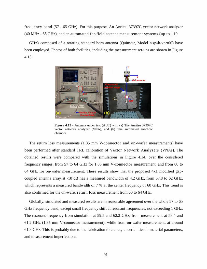
91
frequency band (57 - 65 GHz). For this purpose, An Anritsu 37397C vector network analyzer
(40 MHz - 65 GHz), and an automated far-field antenna measurement systems (up to 110
GHz) composed of a rotating standard horn antenna (Quinstar, Model noqwh-vprr00) have
been employed. Photos of both facilities, including the measurement set-ups are shown in Figure
4.13.
The return loss measurements (1.85 mm V-connector and on-wafer measurements) have
been performed after standard TRL calibration of Vector Network Analyzers (VNAs). The
obtained results were compared with the simulations in Figure 4.14, over the considered
frequency ranges, from 57 to 64 GHz for 1.85 mm V-connector measurement, and from 60 to
64 GHz for on-wafer measurement. These results show that the proposed 4x1 modified gap-
coupled antenna array at -10 dB has a measured bandwidth of 4.2 GHz, from 57.8 to 62 GHz,
which represents a measured bandwidth of 7 % at the center frequency of 60 GHz. This trend is
also confirmed for the on-wafer return loss measurement from 60 to 64 GHz.
Globally, simulated and measured results are in reasonable agreement over the whole 57 to 65
GHz frequency band, except small frequency shift at resonant frequencies, not exceeding 1 GHz.
The resonant frequency from simulation at 59.5 and 62.2 GHz, from measurement at 58.4 and
61.2 GHz (1.85 mm V-connector measurement), while from on-wafer measurement, at around
61.8 GHz. This is probably due to the fabrication tolerance, uncertainties in material parameters,
and measurement imperfections.
Figure 4.13 - Antenna under test (AUT) with (a) The Anritsu 37397C
vector network analyzer (VNA), and (b) The automated anechoic
chamber.

92
As it can be seen from the Figure 4.14 above, the measured return loss using 1.85 mm V-
connector contains some additional amplitude ripples over the considered frequency band (57-65
GHz). This is primarily a result of the unwanted reflections due the mismatch effects between the
50 Ω microstrip feed line and the connector, which are in turn related to the soldering quality of
the V-connector with the 50 Ω microstrip feed line.
The simulated and measured radiation patterns at 60 GHz in both E and H-planes are
presented in Figure 4.15 below.
Figure 4.14 - Measured and simulated return loss of the
fabricated 4x1 gap-coupled antenna arrays.
Figure 4.15 - Radiation patterns of the fabricated 4x1 gap-
coupled antenna array in E and H-planes. .

93
The simulated and measured E-plane patterns agree well with each other, while maintaining
high symmetry and good broadside radiation pattern. However, a certain asymmetry in the H-
plane pattern is observed, which is mainly related to the parasitic elements coupling that makes
the radiation pattern slightly inclined towards the front of the array. The half-power beamwidth
(HPBW) in the E-plane and H-plane are respectively 15º and 91°, and the first side lobe is about
13.46 dB below the main lobe.
The small variations observed between simulated and measured results for both planes in
Figure 4.15, are probably due to the connector losses during radiation pattern measurement and
fabrication tolerances, as mentioned earlier.
The results of the measured and simulated peak gain of the proposed 4x1 gap-coupled array
configuration over the frequency band of 57.5 to 62.8 GHz (at the operating frequency bands)
are shown in Figure 4.16.
These results show more than 10 dB of measured gain in the operating frequency range (-10
dB return loss bandwidth), from 57.8 to 62 GHz with maximum measured peak of 10.7 dB at
61.5 GHz (simulated 11.4 dB at 62 GHz). However, the difference between simulated and
realized gain is more or less 0.95 dB in the considered frequency band. As mentioned previously,
the major part of this loss is due to the additional reflections resulted from the 1.85 mm (V)
connector, which can reach the insertion loss of 1 dB below 67 GHz [29]. In fact, this problem
Figure 4.16 - Simulated and measured gains of the
fabricated 4x1 gap-coupled antenna array.

94
can possibly be avoided given the miniature size of the antenna (does not exceed 5.2 mm by 9.5
mm) which enables it to be easily integrated with other components in the package.
4.5. Conclusion
In this study, an improved gap-coupling concept for 60 GHz millimeter-wave microstrip patch
antennas has been theoretically investigated, and experimentally validated. For this purpose, a
new compact configuration of gap-coupled patch antenna having curved radiating edges has been
designed, fabricated, and tested. The principle is to maintain an optimized coupling level from
driven to the parasitic element through the modification of the current flowing way around the
edges of the patches. This approach may enhance the operational bandwidth to more than four
times and increases the gain up to 3 dB as compared to the single modified patch.
Based on the modified gap-coupled patch (MGCP) antenna element that has proved a better
bandwidth performance compared to the rectangular gap-coupled patch (RGCP) structure, a 4x1
gap-coupled array antenna has been, also designed and fabricated. The obtained results in terms
of bandwidth (7 %), gain (10.7 dB), and compactness (5.2 mm by 9.5 mm), prove evidently a
high optimization level of the proposed structure and make it a serious candidate for integration
in the future broadband millimeter-wave integrated circuits.
Acknowledgment
The authors would like to acknowledge the Natural Sciences and Engineering Research
Council of Canada (NSERC), for the generous research support, and the “Centre de Recherche
en Électronique Radiofréquence” (CREER) of Montréal, funded by the “Fonds de recherche du
Quebec–Natures and technologies” (FRQNT), for the MHMICs fabrication.
95
References
[1] C. A. Balanis, Antenna theory analysis and design, 3rd ed., NY, John Wiley and Sons, 2011.
[2] G. Kumar and K.P. Ray, Broadband Microstrip Antennas, Boston, MA, USA, Artech House,
2003.
[3] S. Liu, W. Wu, and D. G. Fang, “Single-feed dual-layer dual-band E-shaped and U-slot patch
antenna for wireless communication application,”IEEE Antennas Wireless Propag. Lett., vol. 15,
pp. 468–471, 2016.
[4] H. Wong, K. K. So, and X. Gao, “Bandwidth enhancement of a monopolar patch antenna with
V-shaped slot for car-to-car and WLAN communications,” IEEE Trans. Veh. Technol., vol. 65,
no. 3, pp. 1130–1136, Mar. 2016.
[5] X. Zhang and L. Zhu, “Gain-enhanced patch antennas with loading of shorting pins,” IEEE
Trans. Antennas Propag., vol. 64, no. 8, pp. 3310–3318, Aug. 2016.
[6] H. W. Lai, D. Xue, H. Wong, K. K. So, X. Y. Zhang, “Broadband Circularly Polarized Patch
Antenna Arrays with Multiple-Layers Structure,” IEEE Antennas Wireless Propag. Lett., vol. 16,
pp. 525–528, 2017.
[7] W. C. Yang, H. Wang, W. Q. Che, Y. Huang, and J. Wang, “High gain and low-loss millimeter-
wave LTCC antenna array using artificial magnetic conductor structure,” IEEE Trans. Antennas
Propag., vol. 63, no. 1, pp. 390–395, Jan. 2015.
[8] H. Sun, Y.-X. Guo, and Z. Wang, “60-GHz circularly polarized U-slot patch antenna array on
LTCC,” IEEE Trans. Antennas Propag., vol. 61, no. 1, pp. 430–435, Jan. 2013.
[9] R. Florencio, R. R. Boix, and J. A. Encinar, “Fast and accurate MoM analysis of periodic arrays
of multilayered stacked rectangular patches with application to the design of reflectarray
antennas,” IEEE Trans Antennas Propag., vol. 63, no. 6, pp. 2558-2571, June 2015.
[10] R. Azim, M. T. Islam, and N. Misran, “Ground modified double-sided printed compact UWB
antenna,” Electron. Lett., vol. 47, no. 1, pp. 9–11, 2011.
[11] C. K. Aanandan, P.Mohanan, and K. G. Nair, “Broad-band gap coupled microstrip antenna,”
IEEE Transactions on Antennas and Propagation, vol. 38, no. 10, pp. 1581–1586, 1990.
[12] A. Kandwal and S. K. Khah, “A novel design of gap-coupled sectoral patch antenna,” IEEE
Antennas Wireless Propag. Lett., vol. 12, pp. 674–677, 2013.

96
[13] G. Kumar and K. C. Gupta, “Broadband microstrip antennas using additional resonators gap-
coupled to the radiating edges,”IEEE Transactions on Antennas and Propagation, vol. 32, no. 12,
pp. 1375–1379, 1984.
[14] P. Kumar and G. Singh, “Gap-coupling: a potential method for enhancing the bandwidth of
microstrip antennas,” Advanced Computational Techniques in Electromagnetics, vol. 2012,
Article ID acte-00110, 6 pages, 2012.
[15] C. Wood, “Improved bandwidth of microstrip antennas using parasitic elements,” Inst Electr.
Eng Proc.Microw., Opt. Antennas, vol. 127, no. 4, pp. 231–234, 1980.
[16] Q. Song and X. X. Zhang, “Study on wideband gap-coupled microstrip antenna arrays
antennas,” IEEE Transactions on Antenna and Propagation, vol. 43, pp. 313–317, 1995.
[17] C. K. Wu and K. L. Wong, “Broadband microstrip antenna with directly coupled and gap-
coupled parasitic patches”, Microwave Opt. Technol. Lett. 22, 348–349, Sept. 5, 1999.
[18] K. P. Ray, S. Ghosh, and K. Nirmala, “Compact broadband gap-coupled microstrip
antennas,” in Proc. IEEE Antennas Propag. Soc. Int. Symp., vol. 9–14, pp. 3719–3722, 2006.
[19] P. Nayeri, F. Yang, and A. Z. Elsherbeni, “Bandwidth improvement of reflectarray antennas
using closely spaced elements,” Prog. Electromagn. Res. C, vol. 18, pp. 19–29, 2011.
[20] A. A. Deshmukh and K. P. Ray, “Broadband proximity-fed square-ring microstrip
antennas,”IEEE Antennas Propag. Mag., vol. 56, no. 2, pp. 89–107, Apr. 2013.
[21] W.Yang, K.Ma, K.S.Yeo, and W.M.Lim, “A Compact High-Performance Patch Antenna
Array for 60-GHz Applications,” IEEE Antennas and Wireless Propagation Lett., vol. 15, pp.
313–316, 2016.
[22] C. Hannachi, S. O. Tatu, “A New Compact V-band Six-port Down-Converter Receiver for
High Data Rate Wireless Applications,” IEEE Topical Conference on Wireless Sensors and
Sensor Networks (WiSNet), pp. 26–28, San Diego, CA, USA, 25 – 28 January 2015.
[23] Adane, A. Gallée, F. Person, C, "Bandwidth improvements of 60 GHz micromachining patch
antenna using gap coupled U — Microstrip feeder, " Proceedings of the Fourth European
Conference on Antennas and Propagation, pp.1-5, Barcelona, Spain, April, 12-16, 2010.
[24] C. Hannachi, D. Hammou, T. Djerafi, Z. Ouardirhi, and S.O. Tatu, “Complete
Characterization of Novel MHMICs for V-band Communication Systems,” Journal of Electrical
and Computer Engineering, Article ID 686708, pp.1-7, October 2013.

97
[25] C. Hannachi, E. Moldovan, Z. Ouardirhi, and S.O. Tatu, “V-band Six-port Quadrature
Demodulator: Error Vector Magnitude Analysis,” 8th Global Symposium on Millimeter Waves
(GSMM 2015), pp.1-3, Montreal, Quebec, Canada, May 25-27, 2015.
[26] B. K. Kanaujia and A. K. Singh, “Analysis and Design of Gap-Coupled Annular Ring
Microstrip Antenna,” International Journal of Antennas and Propagation, Article ID 792123,
pp.1-5, 2008.
[27] D. Hammou, E. Moldovan, and S.O. Tatu, “'Novel MHMIC Millimeter Wave Power
Divider/Combiner”, 2011 IEEE Canadian Conference on Electrical and Computer Engineering
(CCECE 2011), Conference proceedings, pp. 280-283, Niagara Falls, Ontario, May 8-11, 2011.
[28] E. Moldovan, and S.O. Tatu, “Design and Characterization of Novel W-band Wide-band
Couplers and Six-port Circuit,” European Microwave Week, Conference proceedings, pp. 279-
282, Paris, France, September 6-11, 2015.
[29] M. Hrobak, Critical mm-Wave Components for Synthetic Automatic Test Systems, Berlin,
Germany, Springer Vieweg, 2015.
98
CHAPITRE 5 :
A V-BAND HIGH DYNAMIC RANGE PLANAR INTEGRATED POWER DETECTOR: DESIGN AND CHARACTERIZATION PROCESS
C. Hannachi, B. Zouggari, Razvan I. Cojocaru, T. Djerafi and S.O. Tatu
Volume 59, Issue 11 Pages 2705–2949, March. 2017
Résumé : Dans cet article, un détecteur de puissance opérant dans la bande V (60-65 GHz),
ayant une large plage dynamique, a été conçu et fabriqué en employant un procédé
MHMIC (Miniature Hybrid Microwave Integrated Circuit). Une diode de type Schottky
HSCH-9161 à zéro polarisation opérant en bande millimétrique a été sélectionnée pour la
fabrication du détecteur de puissance proposé. Par ailleurs, une transition entre la ligne
microruban et guide d'ondes rectangulaire (WR12) possédant une large bande d'opération,
ainsi qu'un réseau d'adaptation d'impédance microruban optimisé à l'entrée de la diode,
ont été également employés. Les étapes de conception et de caractérisation ont été détaillées
afin de fournir une méthodologie efficace pour concevoir des détecteurs de puissance à
haute performance tout en tenant compte de la précision, la non-linéarité, ainsi que de la
limitation des dispositifs de mesure. Le prototype de détecteur de puissance fabriqué
démontre une bonne adaptation d'impédance à l'entrée (une bande passante d'environ 3,8
GHz), une haute stabilité de fonctionnement sur une plage de fréquence de 58,5 à 62 GHz,
ainsi qu'une excellente sensibilité (-48 dBm).
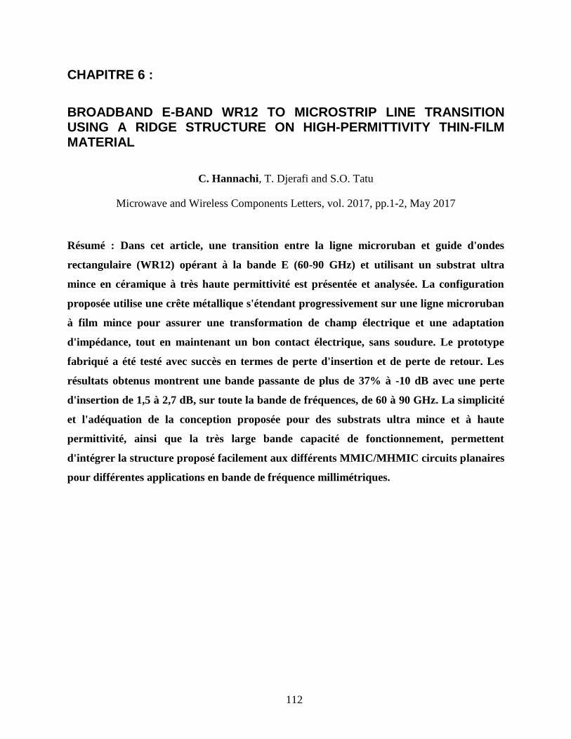
112
CHAPITRE 6 :
BROADBAND E-BAND WR12 TO MICROSTRIP LINE TRANSITION USING A RIDGE STRUCTURE ON HIGH-PERMITTIVITY THIN-FILM MATERIAL
C. Hannachi, T. Djerafi and S.O. Tatu
Microwave and Wireless Components Letters, vol. 2017, pp.1-2, May 2017
Résumé : Dans cet article, une transition entre la ligne microruban et guide d'ondes
rectangulaire (WR12) opérant à la bande E (60-90 GHz) et utilisant un substrat ultra
mince en céramique à très haute permittivité est présentée et analysée. La configuration
proposée utilise une crête métallique s'étendant progressivement sur une ligne microruban
à film mince pour assurer une transformation de champ électrique et une adaptation
d'impédance, tout en maintenant un bon contact électrique, sans soudure. Le prototype
fabriqué a été testé avec succès en termes de perte d'insertion et de perte de retour. Les
résultats obtenus montrent une bande passante de plus de 37% à -10 dB avec une perte
d'insertion de 1,5 à 2,7 dB, sur toute la bande de fréquences, de 60 à 90 GHz. La simplicité
et l'adéquation de la conception proposée pour des substrats ultra mince et à haute
permittivité, ainsi que la très large bande capacité de fonctionnement, permettent
d'intégrer la structure proposé facilement aux différents MMIC/MHMIC circuits planaires
pour différentes applications en bande de fréquence millimétriques.

113
Abstract
A full E-Band (60-90 GHz) WR12 waveguide to microstrip line transition using very thin
high-permittivity ceramic substrate is presented and analyzed. The proposed configuration uses a
gradually extending metal ridge over a thin-film microstrip line to ensure electric field
transformation, and an accurate impedance matching, while maintaining a good electrical
contact, without any soldering or gluing. The fabricated prototype has been, successfully tested
in terms of an insertion and return loss. The obtained results exhibit a bandwidth of more than
37% at -10 dB with insertion loss of 1.5 to 2.7 dB, over the entire 60 to 90 GHz frequency band.
The design simplicity and suitability for high-permittivity thin film substrates, as well as the very
broadband operation capability, enable it to be easily integrated with various planar
MMICs/MHMICs microstrip circuits for different millimeter-wave applications.
6.1. Introduction
The current trend in millimeter-wave technology tends towards increasing component
integration to reduce production time and cost for large-scale production. In this context,
different integration techniques and fabrication processes, including MHMIC (Miniaturised
Hybrid Microwave Integrated Circuits), and MMIC (Monolithic Microwave Integrated Circuits)
are used to provide a reliable interface between different components on a single chip [1, 2].
Indeed, all of those components are, typically interconnected via wire bonding or through
microstrip lines, leading to the realization of more complex systems, such as RF front-end
receivers, or RF transmitter modules. However, the implementation of such systems in practice
often requires the use of the waveguides technology, particularly low loss transitions between
planar microstrip circuits and traditional rectangular waveguides. The later plays a crucial role in
the system's design, and represents a key element for the reliable integration in millimeter-wave
frequency bands, and even beyond [3, 4].
In recent years, several millimeter-wave transition configurations between microstrip lines
and rectangular waveguides have been, investigated in the literature. For instance, antipodal
finline, probe coupling based technique and transition using uniplanar Quasi-Yagi antenna [5].
These transitions exhibit good performances in terms of operating frequency bandwidth and
insertion loss, but involve a high degree of mechanical complexity requiring high-precision
fabrication processes. Transitions based on ridge waveguide have also, been proposed in [6, 7].

114
Although these transitions exhibit a full waveguide band performance and low complexity
structures, only few of them involved high and thin dielectric constant materials. In fact,
millimiter-wave MMICs/MHMICs are often, fabricated on high dielectric constant substrates in
order to allow a high level of integration with various standards of millimiter-wave rectangular
waveguides.
In this letter, an improved design of a rectangular WR12 waveguide to microstrip line
transition using a very thin high-permittivity ceramic substrate (εr = 9.9, h = 127 μm) is
presented and analysed. In the proposed design, a ridge structure with a tapered shape is,
introduced inside the rectangular waveguide to enable a gradual transformation of impedance
and electric field mode, from the rectangular WR12 waveguide to thin-film microstrip line. The
obtained results in terms of impedance bandwidth and insertion loss confirm that the proposed
transition configuration constitutes a serious alternative to the high-permittivity materials,
usually known for their limits to achieve wide bandwidth operation.
6.2. Design and Configuration
The conventional design of transition between rectangular waveguide (RWG) and microstrip
line (MSL), using a ridge-waveguide structure is illustrated in Figure 6.1. In the proposed
transition, the impedance matching and EM field mode transformation between rectangular
waveguide and microstrip line are, mainly managed by gradually extending metal ridge in
rectangular waveguide, until it matches the impedance and the field distribution of microstrip
line. On one hand, this operation allows an accurate impedance matching, from few hundreds of
ohms (characteristic impedance of RWG) to fifty ohms (characteristic impedance of MSL). On
the other hand, enables a gradual transition, from the fundamental TE10 mode of the rectangular
waveguide to the microstrip line quasi-TEM mode [6].

115
The mechanism of the electromagnetic field matching for this arrangement has been detailed
in [6], where a transition between rectangular waveguide and microstrip at K-band has been
designed, and fabricated using thick 5880 RT/Duroid substrate with single sided copper
cladding. Based on similar concept, a new transition configuration employing Duriod based
substrates (ɛr=2.2) at Q-Band was also proposed in [7]. The latter was suggested as a solution to
overcome the difficulties in the mounting reproducibility and DC-block restriction in
applications. A transition from microstrip to ridge gap waveguide was also successfully
implemented at Ka-band using Arlon CLTE-AT substrate (ɛr=3, h=0.254 mm) for integration
purposes of MMIC-based RF circuits with gap waveguide-fed antennas [3].
As may be seen, all the previously mentioned works have only referred to lower permittivity
materials. As can be observed in Figure 6.2a, the standard transition structure is only suitable for
low permittivity substrate with any thickness, and for high permittivity substrate with only thick
thickness.
In this approach, the discontinuity created at the substrate-air junction can be modelled by an
ideal transformer and pure shunt impedance according to [8, 9]. However, the discontinuity
increases with permittivity and inversely proportional to the thickness.
In order to overcome this limitation, simple mechanism should be added to eliminate the
imaginary portion created by the junction effect. In this respect, transmission line of length l1=3
mm and impedance Zfield_RW is introduced to rotate the reflection coefficient Γ toward purely
resistive loads on the Smith chart. Furthermore, the linear ridge taper of lt=4.07 mm has the role
Figure 6.1 - Microstrip-to-ridge waveguide in-line.
transition.
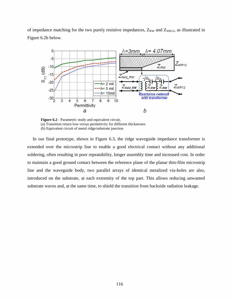
116
of impedance matching for the two purely resistive impedances, ZRW and ZWR12, as illustrated in
Figure 6.2b below.
In our final prototype, shown in Figure 6.3, the ridge waveguide impedance transformer is
extended over the microstrip line to enable a good electrical contact without any additional
soldering, often resulting in poor repeatability, longer assembly time and increased cost. In order
to maintain a good ground contact between the reference plane of the planar thin-film microstrip
line and the waveguide body, two parallel arrays of identical metalized via-holes are also,
introduced on the substrate, at each extremity of the top part. This allows reducing unwanted
substrate waves and, at the same time, to shield the transition from backside radiation leakage.
Figure 6.2 - Parametric study and equivalent circuit,
(a) Transition return loss versus permittivity for different thicknesses
(b) Equivalent circuit of metal ridge/substrate junction

117
6.3. Results and Discussion
The simulated and measured S-parameters are obtained using, respectively, the HFSS
simulation software by Ansoft Corporation, and Keysight (Agilent) Technologies network
analyzer (E8362B) equipped with E-band extension modules, operating in 60 – 90 GHz band.
It should be noted, that the designed transition has been optimized to achieve better
performances, especially over 60 to 65 GHz frequency range to be used for V-band high-speed
communication transceivers. This is due, to the fact that the proposed structure will be
implemented at the input of an integrated MHMIC 60 GHz front-end prototype, currently in
development to enable local oscillator (LO) signal feeding [10]. However, in view of the
achieved broadband performances, this transition remains useable for others millimeter-wave
applications in W-band (70-90 GHz), such as automotive radars and imaging systems.
Figure 6.4 compares the simulated and measured results of insertion and return loss over the
entire 60 to 90 GHz frequency band (a typical operating frequency range of a standard WR-12
waveguide). The obtained results are in good agreement and show a return loss of better than -10
dB. The insertion loss variation achieved over the same frequency band is from 1.5 to 2.7 dB.
Figure 6.3 - Proposed rectangular waveguide to microstrip line transition.
(a) Geometrical structure with the optimized parameters
(b) Photograph of the fabricated ridge structure (top part)
(c) Photograph of the compatible WR12 flange
(d) Photograph of the microstrip structure (bottom part)

118
Nevertheless, frequency response shift of approximately 4% between simulated and measured
return loss is observed. Generally, such frequency shift could be the eventual result of
manufacturing tolerances, uncertainty in substrate thickness, and permittivity deviation
commonly occurring at millimeter-wave bands.
In order to enable comparison with the previous state of the art, the performance of the
proposed transition structure is compared in terms of bandwidth, insertion loss, and complexity
level with other transition recently designed on high permittivity substrate. The results are,
summarized in Table 6.1.
It is clear from the table that the proposed transition structure achieves better performances
compared to other structures. It demonstrates a wider bandwidth (more than 37% at -10 dB),
minimal insertion loss variation (losses from 1.5-2.7 dB over the whole 60 to 90 GHz frequency
band), and lowest complexity (single-layer fabrication process, good electrical contact without
soldering, and easy assembly).
Figure 6.4 - Measured and simulated insertion loss, and
return loss of the fabricated transition prototype.

119
6.4. Conclusion
A broadband WR12 waveguide to microstrip line transition has been proposed and
experimentally demonstrated. The transition structure has been designed to cover the entire E-
band (60-90 GHz), using a very thin high-permittivity alumina substrate (εr = 9.9, h = 127 μm).
In order to highlight the performance, and the reduced complexity of the fabricated structure,
comparison with the previous state-of-the-art has been performed. The obtained results at a
similar permittivity show that the proposed approach is the most appropriate to the thin high-
dielectric-constant materials, commonly known for their difficulty of achieving wide bandwidth
operation. The proposed structure demonstrates better performance in terms of insertion loss,
return loss, and lower manufacturing complexity. These very good performances make the
designed transition attractive for signal transmission from the rectangular WR12 waveguide
components to different planar MHMICs microstrip circuits in different millimeter-wave
applications, including our future 60-GHz transceiver front-end, currently under development.
Table 6.1: State of the art of E-band transitions.
Ref. [1] [2] [4] [5] This work
Freq. (GHz) 52-65 57-63 69.5-87 60-65 60-90
BW (%) @ -
10dB 10.7 5.7 22.7 6.4 37.3
Loss(dB) Min-
Max 2.4-5 0.7-3 2.5-9 1.5-4 1.5-2.7
Dielec. const
(εr) 7.05 9.9 9.5 9.9 9.9
Complexity High Med. High Med. Low

120
References
[1] Lee, J.J., Eun, K. C., Jung, D. Y., and Park, C. S.: ‘A novel GCPW to rectangular waveguide
transition for 60 GHz applications’, IEEE Microwave and Wireless Component Letters, 2009,
19, (2), pp. 80–82
[2] Choi, J. H., Tokuda, K., Ogawa, H., and Kim, Y. H.: ‘Gap-coupled patch-type waveguide-to-
microstrip transition on single-layer dielectric substrate at V-band’, Electronics Letters, 2004, 40,
(17), pp. 1067–1068
[3] Zaman, A. U., Vukusic, T., Alexanderson M., and Kildal, P.-S.: ‘Design of a simple
transition from microstrip to ridge gap waveguide suited for MMIC and antenna integration’,
IEEE Antennas Wireless Propag. Lett., 2013, 12, pp. 1558–1561.
[4] Zhang, Y., Zhao, D., and Reynaert, P.: ‘A Flip-Chip Packaging Design with Waveguide
Output on Single-Layer Alumina Board for E-Band Applications’, IEEE Transactions on
Microwave Theory and Techniques, 2016, 64, (4), pp. 1255–1264
[5] Hammou, D., Nedil, M., Kandil, N., Moldovan, E., and Tatu, S.O.: ‘V-band millimeter-wave
microstrip to rectangular waveguide transition’, Microwave and Optical Technology Letters,
2013, 55, (7), pp. 1696–1699
[6] Ponchak, G. E., and Simons., R. N.: ‘New rectangular waveguide to coplanar waveguide
transition’, IEEE MTT-S Int. Microwave Symp. Dig., 1990, 1, pp. 491–492
[7] Li, J. L., Shao, W., Chen, J. X., and Xue, L. J.: ‘A novel waveguide-to-microstrip transition
for millimeter-wave applications’, International Journal of Infrared and Millimeter Waves, 2004,
25, pp. 513-521
[8] Chang, C. T. M.: ‘Equivalent Circuit for Partially Dielectric-Filled Rectangular-Waveguide
Junctions’, IEEE Transactions on Microwave Theory and Techniques, 1973, 21, (6), pp. 403-411
[9] Angulo, C. M.: ‘Discontinuities in a Rectangular Waveguide Partially Filled with Dielectric’,
IEEE Transactions on Microwave Theory and Techniques, 1957, 5, (1), pp. 68-74
[10] Hannachi, C., Tatu, S.O.: ‘A New Compact V-band Six-port Down-Converter Receiver for
High Data Rate Wireless Applications’. Wireless Sensors and Sensor Networks Conference, San
Diego, January 2015, pp. 26–28

121
CHAPITRE 7 :
FABRICATION, RÉSULTATS ET DISCUSSIONS
7.1. Prototypes des frontales radiofréquences fabriquées
Nous avons en effet, effectué plusieurs tentatives de réalisation de cette frontale
radiofréquence. Ces essais comportaient toujours des erreurs liées à la fabrication (coupure au
laser, mauvaise insertion du circuit dans la cavité, raccordement de microcircuits par fils sur
circuits hybrids, bris du substrat, etc..). Nous étions toujours en contact direct avec les
techniciens afin d’identifier ces problèmes, et améliorer la conception du circuit pour qu’elle soit
adaptée aux exigences technique ou matériel relatives à la fabrication.
Par exemple, lors de la première tentative de fabrication du prototype (voir Figure 7.1), nous
avons rencontré un problème au niveau de l’implantation de l’amplificateur faible bruit (LNA),
plus particulièrement, la conception du circuit de polarisation associé à ce dernier. Par
conséquent, nous avons eu la difficulté à polariser l’amplificateur faible bruit (LNA), ce qui a
engendré un phénomène d'oscillation. Ce problème a été rapidement résolu en implantant deux
condensateurs ayant une valeur de 100 pF, plus proche à l’entrée et à la sortie du l’amplificateur
faible bruit (LNA). Cependant, cette tentative de réparation a engendré d’autres complications
relatives au raccordement par fils (wirebonding), au niveau des entrées de polarisation de
l’amplificateur (LNA), ce qui a empeché l’alimentation en DC de ce dernier.
Suite à cette problématique, nous avons pensé de simplifier notre conception de frontale
radiofréquence en fabriquant un prototype sans l'introduction du l’amplificateur faible bruit LNA
(voir Figure 7.2), et caractériser au même temps ce dernier dans un prototype séparé (prêt à être
caractériser présentement). En effet, le prototype fabriqué a été caractérisé avec succès et les
résultats expérimentaux seront présentés en détail dans ce chapitre. Ces résultats incluent
éventuellement l'évaluation expérimentale de la qualité de la transmission en fonction de
différents types de modulation incluant BPSK, QPSK, 8PSK, 16PSK, 16QAM, et 32QAM, ainsi
que la validation pratique d'une liaison sans fil à 60 GHz en utilisant le prototype de la frontale
radiofréquence fabriquée.
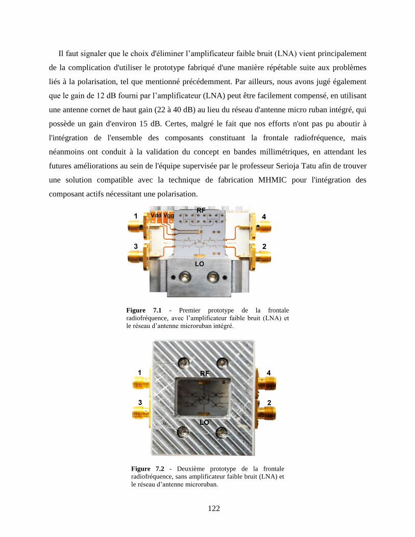
122
Il faut signaler que le choix d'éliminer l’amplificateur faible bruit (LNA) vient principalement
de la complication d'utiliser le prototype fabriqué d'une manière répétable suite aux problèmes
liés à la polarisation, tel que mentionné précédemment. Par ailleurs, nous avons jugé également
que le gain de 12 dB fourni par l’amplificateur (LNA) peut être facilement compensé, en utilisant
une antenne cornet de haut gain (22 à 40 dB) au lieu du réseau d'antenne micro ruban intégré, qui
possède un gain d'environ 15 dB. Certes, malgré le fait que nos efforts n'ont pas pu aboutir à
l'intégration de l'ensemble des composants constituant la frontale radiofréquence, mais
néanmoins ont conduit à la validation du concept en bandes millimétriques, en attendant les
futures améliorations au sein de l'équipe supervisée par le professeur Serioja Tatu afin de trouver
une solution compatible avec la technique de fabrication MHMIC pour l'intégration des
composant actifs nécessitant une polarisation.
Figure 7.1 - Premier prototype de la frontale
radiofréquence, avec l’amplificateur faible bruit (LNA) et
le réseau d’antenne microruban intégré.
Figure 7.2 - Deuxième prototype de la frontale
radiofréquence, sans amplificateur faible bruit (LNA) et
le réseau d’antenne microruban.
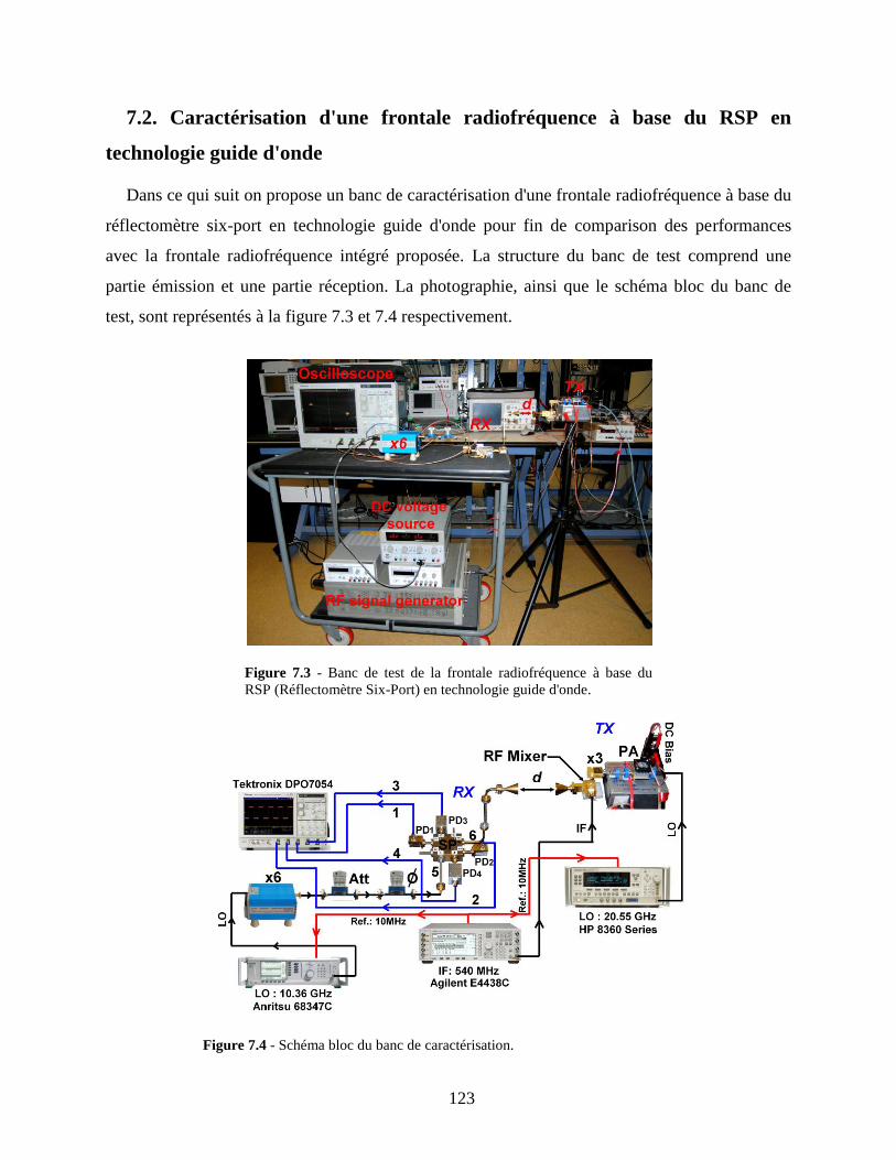
123
7.2. Caractérisation d'une frontale radiofréquence à base du RSP en
technologie guide d'onde
Dans ce qui suit on propose un banc de caractérisation d'une frontale radiofréquence à base du
réflectomètre six-port en technologie guide d'onde pour fin de comparison des performances
avec la frontale radiofréquence intégré proposée. La structure du banc de test comprend une
partie émission et une partie réception. La photographie, ainsi que le schéma bloc du banc de
test, sont représentés à la figure 7.3 et 7.4 respectivement.
Figure 7.3 - Banc de test de la frontale radiofréquence à base du
RSP (Réflectomètre Six-Port) en technologie guide d'onde.
Figure 7.4 - Schéma bloc du banc de caractérisation.
.

124
Les équipements employés dans le banc de test, sont illustrés dans le tableau 7.1 ci-dessous.
La partie émission est composée d’une source vectorielle synchronisée (HP 3860 Series)
délivrant le signal RF à la fréquence de 20.55 GHz. Ce dernier est amplifié et multiplié par le
multiplicateur de fréquence x3 (SFP-123KF-S1) afin d'atteindre une fréquence dans la bande V,
autour de 61.65 GHz. Le signal obtenu est combiné à l'aide d'un mélangeur RF balancé avec le
signal de la fréquence intermédiaire (IF) de 540 MHz provenant de la source Agilent E4438. À
l'émission, une antenne cornet opérant à la bande de 60 GHz, avec un gain d'environ 22 dB, est
employée pour transmettre le signal module a la frequence 61.65 GHz + 0.54 GHz = 62.19 GHz.
La partie réception est constituée du RSP (réflectomètre six-port), de quatre détecteurs de
puissance performants (zero-bias) et d'un atténuateur et déphaseur pour contrôler la puissance et
la phase du signal (LO) en bande millimétrique. Un multiplicateur de fréquence (x6) est
également utilisé afin de générer un signal (LO) à la fréquence de 62.19 GHz, au niveau du port
5 du RSP. Les résultats de démodulation sont affichés directement à l’écran de l’oscilloscope
Tektronix DPO7054 [1-3].
Nous avons donc réussi à obtenir les signaux en phase et en quadrature, I et Q, pour
différentes modulations et vitesse de bits. Les constellations des signaux démodulés, BPSK,
Tableau 7.1-équipements employés au banc de test
Équipements Modèles
Sources vectorielles
- Anritsu 68347C
- Agilent E4438
- HP 3860 Series
Oscilloscope Tektronix DPO7054
Frequency multiplier
module (x3) SFP-123KF-S1
Frequency sixtupler
module (x6) S12MS
Waveguide attenuator DORADO
Phase shifter DORADO
K-Band power amplifier -
Millimeter-wave power
detectors HXI, LLC
Millimeter-wave
balanced mixer HXI, LLC
DC power sources Agilent
E-band conical horn
antennas SAGE Millimeter Inc

125
QPSK, 8PSK ainsi que 16PSK, sont ainsi obtenues et affichées sur l’écran de l’oscilloscope. Les
photographies de ces constellations sont représentées à la figure 7.5, ci-dessus [4-5].
Comme on peut l'observer sur la figure 7.5, les formes des constellations des signaux
démodulées sont légèrement déformées. Cela est dû à plusieurs facteurs, notamment les
imperfections de fabrication, inhérentes en bandes millimétriques, générant des distorsions du
signal RF en amplitude et en phase, ce qui conduit à la détérioration des performances du
récepteur et la qualité de la transmission. On peut distinguer également le problème de fuite OL
(Oscillateur Local) à travers le port RF, ce qui peut engendrer une composante DC, un bruit
supplémentaire, et une distorsion de second ordre. Cependant, pour les schémas de modulation
simples recommandés pour les émetteurs-récepteurs à faible coût, tels que la modulation par
déplacement d'amplitude (ASK), par changement de phase binaire (BPSK), ainsi que par
changement de phase en quadrature (QPSK), une erreur de phase inférieure à 5% est considéré
comme acceptable [6].
Figure 7.5 - Résultats de démodulations
MPSK (1mV/div).
126
7.3. Caractérisation de la frontale radiofréquence à base du RSP en
technologie MHMIC
7.3.1. Simulation système
Dans cette partie, nous allons commencer par évaluer la qualité de la transmission à 60 GHz
d’un système émetteur/récepteur pour des débits binaires simulés de l’ordre du Gb/s. Le système
émetteur/récepteur sera implémenté en utilisant le logiciel ADS (Advanced Design System), tout
en plaçant le RSP dans des conditions réalistes de fonctionnement (gain d’antenne, puissances
RF et LO, distance émetteur-récepteur, gain et figure de bruit du LNA, …etc) tel qu'illustré dans
la figure 7.6.
Telle qu'illustrée dans la la figure 7.6, le récepteur est composé d’une antenne réceptrice, d’un
amplificateur faible bruit (LNA), ainsi que du réflectomètre six-port (RSP) connecté aux quatre
détecteurs RF et de deux amplificateurs vidéo. Pour la mise en forme des signaux I/Q, on a
utilisé des filtres et des circuits "sample-and-hold (SHC) ". La propagation du signal RF est
simulée en utilisant la composante LOS_Link, fournie par la librairie composant du logiciel
ADS, basée sur le modèle de Friis.
On va évaluer donc la qualité de la transmission en fonction de différents types de modulation
incluant BPSK, QPSK, 8PSK, 16PSK, 16QAM, 32QAM [6].
Nous avons réussi à obtenir les signaux en phase et en quadrature, I et Q, pour différentes
modulations. Les constellations des signaux démodulés à une vitesse de 1 Gbits/s sont affichées
dans la figure 7.7 ci-dessous.
Figure 7.6 - Schéma bloc du circuit de simulation du récepteur à base du réflectomètre six-port.
127
Comme on peut le constater dans la figure, les symboles des démodulations 8PSK et 16PSK
sont répartis uniformément autour du cercle. De même, pour le diagramme de constellation
QPSK, on obtient une forme quasi-parfaitement carrée. Par ailleurs, pour les constellations
16QAM, 32QAM, les points sont presque équidistants, ce qui prouve bien la qualité du RSP
comme discriminateur d'amplitude et de phase, suivant ainsi la théorie de démodulateur six port
[4]. Les erreurs de phase et d'amplitude sont minimales, ne dépassant pas quelques pourcentages
pour chaque point de constellation. On rappelle que le modèle du RSP dans la simulation
système proposée est obtenu à partir des mesures sur les différents circuits à deux ports. Par
conséquent, les erreurs de modèle comprennent des erreurs de fabrication d'un circuit à l'autre et
des erreurs de mesure et de configuration de la station VNA (des erreurs de phase liées à la
position de la sonde coplanaire de GSG-150 (150μm)). On peut noter par exemple que pour une
erreur de 10 μm, une erreur de phase de 2° peut être engendrée.
Figure 7.7 - Diagrammes simulés de constellation
PSK/QAM des signaux I et Q.
128
7.3.2. Mesure et caractérisation
Dans cette partie, nous allons réaliser un montage similaire à celui dans la Figure 7.4, en
remplaçant cette fois la frontale radiofréquence à base de guide d'onde par la frontale
radiofréquence intégré en technologie MHMIC. Le nouveau montage de carctérisation est illustré
dans la Figure 7.8.
Cette fois, la source vectorielle synchronisée (HP 3860 Series) délivrant le signal RF à la
fréquence de 20.57 GHz. Ce dernier est amplifié et multiplié par le multiplicateur de fréquence
x3 (SFP-123KF-S1) afin d’assurer une fréquence autour de 61.71 GHz (band V). Le signal
obtenu est combiné à l'aide d'un mélangeur RF balancé avec le signal de la fréquence
intermédiaire (IF) de 600 MHz (source Agilent E4438). Une antenne cornet opérant à la bande
de 60 GHz, avec un gain d'environ 22 dB, est également employée pour transmettre le signal
modulé.
Lors de la caractérisation experimentale, nous avons également pu obtenir les signaux en
phase et en quadrature, I et Q, pour différentes modulations. Les constellations des signaux
démodulés sont affichées dans la figure 7.9 ci-dessous.
Comme on peut le remarquer dans la figure, les symboles des démodulations 8PSK et 16PSK
sont répartis uniformément autour du cercle et concordent fort bien avec les résultats des
Figure 7.8 - Schéma bloc du banc de caractérisation d'un récepteur basé sur un six-port
intégré en technologie microstrip.

129
simulations obtenus précédement. Pareillement, pour la constellation de la démodulation QPSK,
on obtient une forme carrée qui est presque comparable à celle obtenue lors de la simulation.
Pour les constellations 16QAM, 32QAM, les points sont uniformément répartis et correspondent
également bien aux résultats de simulation ADS.
7.3.3. Validation expérimentale d'une liaison sans fil à 60 GHz
Dans ce qui suit, nous allons examiner la faisabilité d'une liaison sans fil à 60 GHz pour des
courtes distances (1-1.75m), en utilisant la frontale radiofréquence fabriqué. Pour se faire, on
garde la même configuration dans le montage précédant (voir Figure 7.8), sauf que cette fois on
utilise une antenne cornet de haut gain (environ 40 dB), ainsi qu'une lentille spéciale placée à
environ 10 cm du récepteur et qui permet d'amplifier le gain de l'antenne réceptrice afin d'aller à
des distances plus longues. Toutefois, il faut bien signaler que ces mesures ont été prises pour
contourner certaines limitations au niveau des équipements de mesure, notamment les
Figure 7.9 - Diagrammes expérimentaux de
constellation PSK/QAM des signaux I et Q (1
mV/div).
130
restrictions relatives à la bande passante et le niveau de puissance permis. Le montage
expérimental de cette liaison est illustré dans la Figure 7.10.
Nous avons également pu afficher les formes d’ondes des signaux I et Q pour différents types
de démodulation incluant BPSK, QPSK, 8PSK, et 16QAM dans le domaine temporel à l'aide de
l'oscilloscope, tel que présenté dans les Figures 7.11, 7.12, 7.13, et 7.14.
Figure 7.10 - Photographe du banc de caractérisation du récepteur à base du réflectomètre
six-port pour une liaison sans fil de 1.75m.
Figure 7.11 - Formes d’ondes des signaux I et Q pour une modulation BPSK.

131
Figure 7.12 - Formes d’ondes des signaux I et Q pour une modulation QPSK.
Figure 7.13 - Formes d’ondes des signaux I et Q pour une modulation 8PSK.

132
Comme on peut le constater, les résultats dans ces Figures illustrent bien les sauts de phase du
signal RF qui correspondent à des multiples de 90°.
7.3.4. Évaluation de la liaison à 60 GHz
Dans cette partie, nous allons présenter les principaux paramètres influant la qualité d'une
liaison radio haut débit à 60 GHz. En effet, la propagation des ondes électromagnétiques à la
bande 60 GHz est caractérisée par un niveau élevé d'absorption de l'oxygène (une atténuation de
17 dB/Km) et de l'atténuation de la pluie, tout en ajoutant l'atténuation de propagation donnée
par la formule conventionnelle de Friis. Ces effets limitent remarquablement la portée des
systèmes de communication exploitant cette bande de fréquence, cependant elle permet la
réutilisation de fréquence, ce qui la rend très attractive pour nombreuse applications de
communication à courte portée. La frontale radiofréquence proposée dans le cadre de cette thèse
est également conçue pour fonctionner a des distances courtes de 1 à 10 mètres, avec un rapport
signal sur bruit (S/N) out d'environ 16 dB [7].
Figure 7.14 - Formes d’ondes des signaux I et Q pour une modulation 16QAM.
133
Dans ce qui suit, nous allons évaluer l’atténuation dans l’espace libre, dans un canal de
transmission 60 GHz. Considérant ces conditions, La puissance reçue peut être exprimée selon
l’équation de Friis [7]:
Dans cette expression Gt et Gr correspondent respectivement aux gains des antennes de
l’émetteur et du récepteur. Pt, est la puissance transmise et Pr, est la puissance reçue. En espace
libre, les pertes dues au canal de transmission, sur une distance d, s’expriment par :
On peut déterminer aisément à partir de cette équation, l’atténuation du canal de transmission
à 60 GHz. Elle est estimée à -48 dB pour une distance de 1.75 mètres et à -88 dB pour une
distance de 10 mètres. Si on dispose d’une puissance à l’émission de 10 dB, et un gain d’antenne
à l’émission et à la réception de 40 dB et 20 dB respectivement (gain de l'antenne cornet haut
gain utilisée à l’émission, ainsi que l'antenne cornet standard à la réception). La puissance reçue
incluant les pertes à l’émission et à la réception, ainsi que les pertes de trajet, calculée à partir de
la relation de Friis, est estimée à -35 dBm.
7.3.5. Sensibilité du récepteur
Parmi les principaux objectifs du bilan de liaison à 60 GHz est de déterminer la puissance de
réception minimale nécessaire pour obtenir un rapport signal bruit S/N souhaité et par
conséquent une qualité de communication satisfaisante. Cette puissance minimale Prmin définit
cependant la sensibilité du récepteur et s'exprime en fonction du rapport signal à bruit S/N ainsi
que la puissance disponible de bruit FkTB à l’entrée du récepteur [8].

134
k : Constante de Boltzmann.
T: Température ambiante 298 K ou température du récepteur.
B : correspond à la bande passante du récepteur et dépend du débit mais aussi du schéma de
modulation.
Généralement, la sensibilité est exprimée en fonction du rapport Eb/No qui sert de référence
pendant la comparaison du rendement énergétique de plusieurs modulations. En effet,
l'introduction des paramètres No = N/B et Eb = S/Db, correspondant respectivement à la densité
spectrale de bruit ainsi que à l'énergie moyenne par bit, on peut alors exprimer le rapport signal à
bruit S/N par la formule suivante.
La sensibilité du récepteur s'exprime maintenant en fonction du débit binaire Db et du rapport
signal sur bruit normalisé Eb/No.
Cette relation montre clairement que la puissance minimale nécessaire croît avec le débit. À
titre d'exemple, un débit de 100 Mb/s contre 10 Mb/s exige un niveau de puissance à la réception
supérieure à 10 dB afin de garantir une capacité de communication identique [8-9].
135
References
[1] P. Smulders, P, “Exploiting the 60 GHz band for local wireless multimedia access: prospects
and future directions”. IEEE Communications Magazine, vol. 40, no. 1, pp. 140–147, 2002.
[2] S. O. Tatu, E. Moldovan, G. Brehm, K. Wu et R.G. Bosisio, “Ka-Band Direct Digital
Receiver”. IEEE Transactions on Microwave Theory and Techniques, vol. 50 no. 11, pp., 2436 -
2442, 2002.
[3] S. O. Tatu, E. Moldovan, K. Wu, R.G. Bosisio et T. Denidni, “Ka-Band Analog Front-End
for Software-Defined Direct Conversion Receiver”. IEEE Transactions on Microwave Theory
and Techniques, vol. 53, no. 9, 2678 - 2776, 2005.
[4] C. Hannachi, S. O. Tatu, “An Improved-Performance V-band Six-Port Receiver for Future
5G Short-Range Wireless Communications” 2017 IEEE Topical Conference on Wireless Sensors
and Sensor Networks (WiSNet), Phoenix, Arizona, January 15 – 18, 2017.
[5] C. Hannachi, S. O. Tatu, “A New Compact V-band Six-port Down-Converter Receiver for
High Data Rate Wireless Applications” Wireless Sensors and Sensor Networks Conference, San
Diego, January 2015, pp. 26–28.
[6] C. Hannachi, E. Moldovan, Z. Ouardirhi, S. O. Tatu, “V-band Six-port Quadrature
Demodulator : Error Vector Magnitude Analysis”, 8th Global Symposium on Millimeter-Waves
(GSMM2015), Conference Proceedings, Montreal, Canada May 25-27, 2015.
[7] Pozar, D. M. 2005. Microwave Engineering, 3rd ed. New York: Wiley.
[8] S. O. Tatu. 2005. “Nouveau récepteur six-port en ondes millimétriques”. Thèse de doctorat,
Montréal, École polytechnique, 209p.
[9] D. Hammou, E. Moldovan et S. O. Tatu. “60 GHz MHMIC Six-Port Model Analysis”,
Microwave and Optical Technology Letters, Vol. 52, No. 9, September 2010.

136
Conclusion générale et perspectives
Les travaux exposés dans ce mémoire porte sur la fabrication et la caractérisation
expérimentale, de nouveaux circuits millimétriques en technologie MHMIC, destinés à la future
génération des systèmes de télécommunications sans fil.
Nous avons tout d'abord conçu et validé le fonctionnement de circuits de base aux fréquences
millimétriques, incluant, le coupleur hybride arrondi H-90°, le coupleur en anneau (rat-race),
diviseurs/combineurs de puissance de type Wilkinson, ainsi que le réflectomètre six-port. Les
résultats de mesure de tous ces circuits ont été confirmés par les résultats de simulation en
utilisant le logiciel ADS Momentum (Advanced Design Systems software of Keysight
Technologies). Les circuits conçus sont large bande avec un haut degré d’équilibre en amplitude
et en phase, ce qui nous a encouragés d'entamer une nouvelle étape qui consiste à intégrer ces
circuits dans une topologie finale de frontale radiofréquence. Dans ce contexte, le réflectomètre
six-port proposé constituera le noyau du système millimétrique proposé.
Nous avons par ailleurs mené une étude sur les antennes patchs microrubans, et nous avons
développé un nouveau réseau d'antenne de quatre éléments (à base du diviseur/combineur en
anneau). Les résultats de simulation et de caractérisation expérimentale de ces antennes, ont
démontrés de bonnes performances en termes de perte d'insertion, de gain, et d'efficacité.
Un détecteur de puissance à base de diode Schottky a été également conçu et fabriqué dans le
but de l'intégrer aux sorties du réflectomètre six-port, dans le cadre de la frontale radiofréquence
proposée. Les résultats de mesure ont montré des performances globales très acceptables, en
termes d’adaptation, de coefficient de transfert, de sensibilité, et de la largeur de plage
dynamique.
Nous avons aussi conçu et fabriqué dans le cadre de ces travaux, une transition opérant en
bande millimétrique. Cette transitions permit d’interconnecter, différents supports de
transmission tel que : ligne microruban, guide intégré au substrat, et guide d’onde rectangulaire.
La transition de ligne microruban vers guide d’onde rectangulaire WR12 est réalisée dont
l’objectif est d’alimenter notre prototype de frontale radiofréquence en signal de pompe OL
(Oscillateur local). C’est ainsi qu’on assure la synchronisation entre les signaux OL et RF dans la
configuration de frontale radiofréquence proposée.
137
À la fin de ces travaux, nous avons réalisé le prototype final de la frontale radiofréquence à 60
GHz, incluant tous les circuits conçus dans la présente étude. Les résultats de caractérisation
confirment bien que le réflectomètre six-port permet la conception d’architecture de frontale
radiofréquence, de haute performance, intégrée et à faible coût, pour les futurs récepteurs de
communication sans fil à haute débit. Cependant, un point très essentiel reste à améliorer, qui est
la répétabilité des processus de fabrication actuels afin de permettre des meilleurs résultats, au
niveau de la robustesse des circuits intégrés et les prototypes fabriqués. Plus précisément, la
partie qui concerne l'intégration des composants actifs, tels que les amplificateurs à faible bruit
(LNAs). Dans ce contexte, nous avons envisagé de caractériser séparément et d'une manière plus
approfondie et détaillée l'amplificateur à faible bruit utilisé dans le cadre de la frontale
radiofréquence fabriquée. Cela va nous permettre de bien connaitre en effet, le comportement de
l'amplificateur LNA utilisé et communiquer par la suite, des informations pertinentes aux
techniciens afin d'améliorer en continu les méthodes existantes d'assemblage et de fabrication.
Une autre alternative peut être également envisagée, qui est le remplacement de l'amplificateur
LNA actuel par un autre plus robuste et plus adapté au processus de fabrication adopté.
Aujourd’hui, la technologie de communication à ondes millimétriques dans la bande de
fréquences de 60 GHz est en plein essor, et les composants actifs dans différentes technologies
(AsGa, CMOS,..) opérant dans cette bande ont tendance à se multiplier, donc plus de choix, et
plus de composants de qualité seront disponibles au futur.
En fin, nous avons également pensé à diminuer la vulnérabilité des circuits conçus dans le
futur, en optant pour des substrats en céramique plus épais et plus résistants (10 mil et plus),
permettant plus de maniabilité pendant le processus de fabrication. Cependant, le niveau élevé de
la complexité des circuits conçus sur cette substrat demeure le prix à payer.

138
Liste des publications
Journaux
[1] C. Hannachi, T. Djerafi, and S.O. Tatu, “A Novel Broadband Low-Loss Microstrip Line to
Ridged-Waveguide transition Using a Thin Ceramic for Millimeter-wave Applications”,
Microwave and Wireless Components Letters, vol. 2017, pp.1-2, May 2017. (accepted with
major revisions)
[2] C. Hannachi, B. Zouggari, Razvan I. Cojocaru, T. Djerafi, and S.O. Tatu, “A V-band High
Dynamic Range Planar Integrated Power Detector: Design and Characterization Process,”
Microwave and Optical Technology Letters, pp. 1–5, March. 2017. (accepted)
[3] C. Hannachi, and S.O. Tatu, “A Compact V-band Planar Gap-coupled 4x1 Antenna Array:
Improved Design and Analysis”. IEEE Access. Antennas Propag., vol. 5, pp.1-8, February 2017.
(published)
[4] C. Hannachi, and S.O. Tatu, “Performance Comparison of Miniature Printed MHMICs
Patch Antennas with Different Geometrical Shapes for 60-GHz Wireless Applications,” IET
Microwaves Antennas & Propagation, vol. 11, no. 1, pp. 106-112, Januray 2017. (published)
[5] C. Hannachi, D. Hammou, T. Djerafi, Z. Ouardirhi, S.O. Tatu, “Complete Characterization
of Novel MHMICs for V-band Communication Systems”. Journal of Electrical and Computer
Engineering, vol. 2013, Article ID 686708, pp.1-7, October 2013. (published)
Conférences
[1] B. Zouggari, D. Hammou, C. Hannachi, and S. O. Tatu, “Precise Direct Millimeter Wave
QPSK Modulator for 5 G Wireless Communications” 2018 IEEE Topical Conference on
Wireless Sensors and Sensor Networks (WiSNet), Anaheim, CA, January 14 – 17, 2017
(Submited).
[2] C. Hannachi, S. O. Tatu, “Highly Isolated Broadband Five-port Circuit for V-Band High
Data-rate Wireless Communications” The 28th Annual IEEE International Symposium on
Personal, Indoor and Mobile Radio Communications (IEEE PIMRC 2017), Montreal, QC,
October 8 – 13, 2017 (Submited).
[3] C. Hannachi, B. Zouggari, and S.O. Tatu, “Low-cost High Data-rate Direct-Conversion
Multi-port Receiver for Millimeter-wave Indoor Wireless Applications,” International Union of

139
Radio Science General Assembly & Scientific Symposium (URSI 2017), pp. 4–9, Montreal,
August 2017.
[4] C. Hannachi, S. O. Tatu, “An Improved-Performance V-band Six-Port Receiver for Future
5G Short-Range Wireless Communications” 2017 IEEE Topical Conference on Wireless Sensors
and Sensor Networks (WiSNet), Phoenix, Arizona, January 15 – 18, 2017 (Accepted).
[5] B. Zouggari, C. Hannachi, E. Moldovan, and S. O. Tatu, “Millimeter Wave Six-Port QPSK
Modulators for High Data-Rate Wireless Communications”, European Conference, 2016
European Microwave Week, Conference Proceedings, London, United Kingdom October 3-7,
2016 (Accepted)
[6] C. Hannachi, B. Zouggari, and S. O. Tatu, “A compact, High Gain and High Efficiency 8×2
Patch Antenna Array for 60 GHz Communication Systems”, 17th International Symposium on
Antenna Technology and Applied Electromagnetics (ANTEM 2016), Conference Proceedings,
Montreal, Canada, July 10-14, 2016.
[7] E. Dailleux, J-F. Frigon, C. Hannachi, S. O. Tatu, “Millimeter Wave Spatial Multiplexing:
Feasibility and Performance of a Short Range 2x2 Link”, European Conference, 2015 European
Microwave Week, Conference Proceedings, Paris, France September 6-11, 2015.
[8] C. Hannachi, E. Moldovan, Z. Ouardirhi, S. O. Tatu, “V-band Six-port Quadrature
Demodulator : Error Vector Magnitude Analysis”, 8th Global Symposium on Millimeter-Waves
(GSMM2015), Conference Proceedings, Montreal, Canada May 25-27, 2015.
[9] C. Hannachi, S. O. Tatu, “A New Compact V-band Six-port Down-Converter Receiver for
High Data Rate Wireless Applications” 2015 IEEE Topical Conference on Wireless Sensors and
Sensor Networks (WiSNet), San Diego, CA, January 25 – 28, 2015.
[10] T. Jiang, D. Hammou, C. Hannachi, M. Nedil, J-F. Frigon, K. Wu, S. O. Tatu, “Six-port
Technology for Millimeter Wave MIMO Systems”, European Conference, 2013 European
Microwave Week, Conference Proceedings, Nuremberg, Germany October 6-11, 2013.