Embed Size (px)
Citation preview
de Montmorillon et al. Vol. 13, No. 10 /October 1996 /J. Opt. Soc. Am. B 2341
Correlations between microscopic properties andthe photorefractive
response for vanadium-doped CdTe
L. A. de Montmorillon, Ph. Delaye, and G. Roosen
Institut d’Optique, Unite de Recherche Associee 14 au Centre National de la Recherche Scientifique, Bat. 503,Centre Scientifique d’Orsay, B.P. 147, 91403 Orsay Cedex, France
H. Bou Rjeily, F. Ramaz, and B. Briat
Laboratoire d’Optique Physique, Unites propres de Recherche A0005 du Centre National de la RechercheScientifique, Ecole Superieure de Physique et Chimie Industrielle, 10 rue Vauquelin, 75231 Paris Cedex 05, France
J. G. Gies, J. P. Zielinger, and M. Tapiero
Institut de Physique et Chimie des Materiaux de Strasbourg, Unite mixte 380046, Centre National de la RechercheScientifique, Universite Louis Pasteur, Ecole Europeenne des Hautes Etudes des Industries Chimiques de
Strasbourg, Groupe d’Optique Nonlineaire et d’Optoelectronique, 23 rue du Loess,F-67037 Strasbourg Cedex, France
H. J. von Bardeleben
Groupe de Physique des Solides, Unite de Recherche Associee 17 au Centre National de la Recherche Scientifique,Universite Paris 6 et 7, 2 Place Jussieu, 75231 Paris Cedex 05, France
T. Arnoux and J. C. Launay
Action Aquitaine de Recherche en Apesanteur, B.P. 11, 33165 Saint Medard en Jalles Cedex, France, and Institut deChimie de la Matiere Condensee de Bordeaux, Av. du docteur A. Schweitzer, 33608 Pessac Cedex, France
Received February 12, 1996; revised manuscript received April 26, 1996
We present a summary of the experimental results, the attempts of interpretation at the present stage, and theconclusions of coupled investigations on semi-insulating, n-type and p-type vanadium-doped CdTe crystals.Combining electron paramagnetic resonance and magnetic circular dichroism permits the monitoring and thequantitative assessment of [ V 21] and [ V 31] defect concentrations. Photoabsorption results are presentedand are discussed in terms of photoionization processes at various wavelengths. The temperature and thespectral dependence of the steady-state photoconductivity are carefully studied in the near infrared. The re-sults are discussed in terms of electronic transitions for the two vanadium charge states. Finally, the photo-refractive performances of the semi-insulating sample are analyzed in a two-beam-coupling experiment andare correlated to the properties of the V 21/V 31 donor states to derive photoionization cross sections. © 1996Optical Society of America.
1. INTRODUCTION
We have shown in a recent paper1 that the combination ofdifferent measurements permits a good simulation of thephotorefractive properties of GaAs crystals. We usedelectron paramagnetic resonance (EPR) measurements todetermine the EL21 concentration and absorption mea-surements to determine the total EL2 concentration andtook the photoionization cross sections in the literature tocalculate the expected photorefractive gain of our sampleat different wavelengths and to compare it with the ex-perimental data. The results were found to be consis-tent, confirming that the EL2 defect was the deep defectresponsible for the photorefractive effect in GaAs andthat the photorefractive model of one defect coupled to
0740-3224/96/1002341-11$10.00
both conduction and valence bands explained well thephotorefractive performances in this material.In this paper we use a similar approach for another
photorefractive material, vanadium-doped cadmium tel-luride (CdTe:V). This photorefractive material is pres-ently the object of great interest as a promising candidatefor a use in metrology systems and optical telecommuni-cation networks in the wavelength range from 1 to 1.55mm. Beyond the control of imperfections and residualimpurities, one of the problems is to learn which factorscontrol the concentrations of V 21 and V 31 ions in CdTe:V.To this end it is important to be able to determine thethermal and the optical signatures of both ions and theirrespective roles as absorption, trapping, or recombinationcenters, as well as their respective concentrations. To
© 1996 Optical Society of America
2342 J. Opt. Soc. Am. B/Vol. 13, No. 10 /October 1996 de Montmorillon et al.
Table 1. Electrical Characteristics of the Different Samples Studied in the PC Experimentsa
Sample Type NatureDark Resistivity (V cm) at
Room TemperatureActivationEnergy (eV)
L825 Intrinsic Undoped CdTeStarting material
108 0.76
B23 n CdTe:V 131010 0.75B28 p As-codoped CdTe:V 33109 0.74B19 n Cl-codoped CdTe:V 63108 0.51
aL825 is an undoped CdTe crystal used as a reference sample.
see the V 21 (V 31) charge state independently, codopingwith Cl (As) transforming semi-insulating CdTe:V into n-(p-) type crystals is used. Table 1 indicates some of theproperties of these crystals. We perform in these CdTe:Vsamples different optical, electrical, and photorefractive(in the semi-insulating one) measurements that give usinformation about deep defects and their optical proper-ties. Then the determined parameters are combined, al-lowing us to identify the deep level involved in the photo-refractive effect.Section 2 deals with an EPR study of the different crys-
tals. The EPR results have allowed us to determine theFermi-level position and the corresponding V configura-tions in the codoped samples, to measure quantitativelythe V 31 defect concentrations2–7 and to test the directlyphotoinduced variations of the V 31 charge state in thesemi-insulating (B23) sample. Section 3 deals with amagneto-optical study of the different crystals. This in-cludes magnetic circular dichroism (MCD) and optical ab-sorption spectroscopy. By use of EPR for the quantita-tive assessment of [ V 31] in at least one sample, MCDprovides both [V 31] and [V 21]. Linked to this, photoab-sorption data give information about the photogenerationof carriers from the identified deep levels. Section 4 con-cerns photoconductivity (PC) studies. We measure thetemperature dependence of the steady-state PC gain atthe intrinsic maximum (band-to-band excitation), as wellas the steady-state spectral response of PC at constantphoton flux for varying temperatures of as low as 81 K.Section 5 deals with detailed photorefractive measure-ments on sample B23. Section 6 is a general discussionconcerning the correlations among all our results to pro-vide information about spectroscopic assignments,charge-transfer processes, or photoionization cross sec-tions. The paper ends with a brief summary.
2. ELECTRON PARAMAGNETICRESONANCE STUDIESTo associate the different optical absorption bands withthe particular charge states of the V donor we prepareddonor, Cl (B19), and acceptor, As (B28), codoped samples.As the V donor introduces a deep level at 'Ec 2 0.8 eV,the EPR observation of the neutral shallow donor Cl0
with a level at Ec 2 0.02 eV or the deep ionized donorFe31 (residual contamination) with a level at Ev 1 0.35eV allows us to conclude whether the V donor is com-pletely in the V 21 or the V 31 charge state. Figure 1shows the EPR spectra of the B19, the B23, and the B28
samples. In sample B19 only the spectrum of the Cl ef-fective mass donor with a g factor g ' 1.7 is observed.In this sample the V donor is in the V 21 charge state.Even though this state is equally paramagnetic, the cor-responding EPR spectrum is not observed; this has beenattributed to the strain sensitivity of the orbital tripletground state. Sample B19 is used below to identify theV 21-related absorption bands; in contrast, in the acceptor(As) codoped sample (B28), we observe in thermal equilib-rium the Fe31 resonance, which allows us to situate theFermi-level below Ev 1 0.35 eV and thus below the V do-nor level. Sample B28 is used below for identification ofthe V 31-related optical absorption bands.For the modeling of the photorefractive properties of
sample B23 the absolute V 31 concentration is required; ithas been determined by comparison with a spin-standardsample.The photoionization of the V donor in sample B23 can
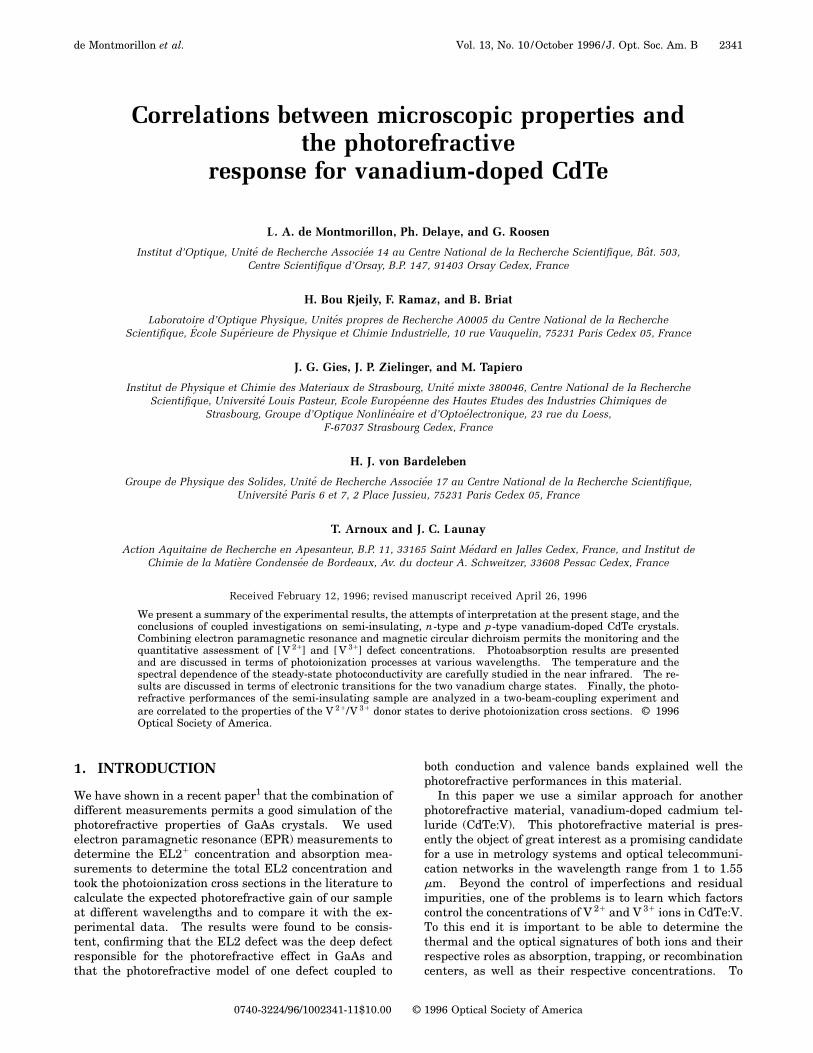
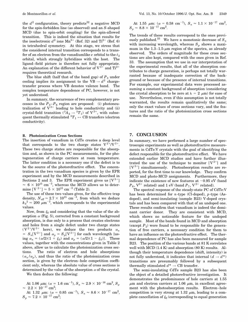
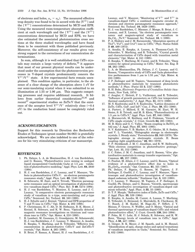
also be directly studied by EPR by means of the associ-ated changes in the V 31 concentration. We tested the in-fluence of an optical excitation at the two relevant wave-lengths of 1.06 and 1.4 mm. As shown in Fig. 2, a1.06-mm excitation increases the V 31 concentration,whereas the 1.4-mm excitation is associated with a de-crease of the V 31 concentration. From this result we can
Fig. 1. EPR spectra of the three samples B19, B23, and B28 atT 5 4 K and Bi[100]. In the n-type (B19) codoped sample onlythe donor resonance is seen, in B23 we observe only the V 31
spectrum (no V 21), and in the p-type codoped sample B28 bothV 31 and Fe31 (Fe contamination) is observed.
de Montmorillon et al. Vol. 13, No. 10 /October 1996 /J. Opt. Soc. Am. B 2343
qualitatively conclude that the associated photoionizationcross sections for electrons (Sn) and holes (Sp) are Sn. Sp at 1.06 mm and Sn , Sp at 1.4 mm.
3. MAGNETO-OPTICAL AND OPTICALABSORPTION STUDIESA. Magnetic Circular DichroismMCD is the differential absorption (Da in cm21) for left(s1) and right (s2) circularly polarized lights propagatingalong the direction of an applied magnetic field B (typi-cally 2.5 T). The MCD signal contains, in general, a dia-magnetic as well as a paramagnetic part, but the former
Fig. 2. (a) EPR spectrum of sample B23 at thermal equilibriumat T 5 4 K. (b), (c) Difference spectra (spectrum under photo-excitation minus spectrum in thermal equilibrium). At 1.4 mm(b), we thus observe a decrease in the V31 intensity; at 1.06 mm(c), an increase, always compared with the thermal equilibriumvalue. Typical excitation intensities are 10 mW cm22, and thespectrum intensity achieves an equilibrium value after typicallya few minutes.
can safely be ignored in our case because the bands arebroad, and we conduct our work at T < 4.2 K. In thecase of, e.g., V 31 (with a 3A2 ground state), the paramag-netic terms are proportional to (n2 2 n1)/(n0 1 n2
1 n1), where n1 , n2 , and n0 stand for the Boltzmannpopulations of the ms 5 61 and the ms 5 0 substates.In a recent paper8 we demonstrated that this technique
permits the simultaneous monitoring at T < 4.2 K of thetwo paramagnetic species [V 21] and [V 31] in CdTe:Vcrystals. It was further used in the case of Zn–Cd alloys9
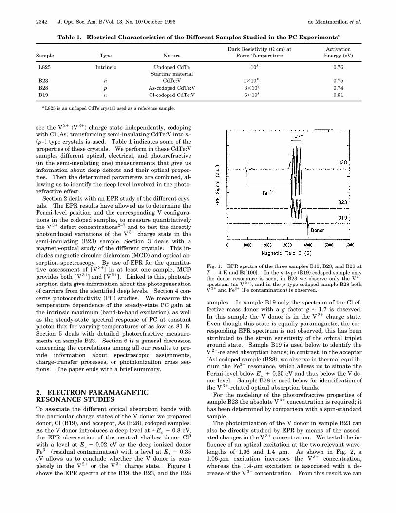
to show that V 31 was present in them, although EPRfailed to detect it directly.Figure 3 shows additional results for our reference
crystal B23 (semi-insulating) as well as for n-type (B19)and p-type (B28) samples. Following our formerresearch,8 the various MCD features are referred to asP1 , P2 , . . ., P5 (or 1. . .5 for short). Band P1 is associ-ated with the major MCD band peaking at ;1.17 eV(9500 cm21). As expected, samples B19 and B28 indeedpresent a completely different behavior. Below 1.05 eV[Fig. 3(a)] the former shows only P2 , whereas the latterpresents two major bands, P3 and P4 , and a relativelysharp negative peak, P5 . A Gaussian analysis actuallystrongly suggests the presence of an additional broadcomponent, P6 , on the high-energy side of P4 . Weassigned8 P5 to the
3A2 → 1E spin-forbidden band of V 31
on the basis of its sharpness and negative MCD. It isquite remarkable (Fig. 3) that the MCD spectra ofsamples B19 (multiplied by 1.4) and B23 superimposeeach other in the regions of bands P1 and P2 . This con-firms our earlier findings8 with two other crystals (B16and B21), and we assign both bands to V 21.The low-energy MCD of sample B23 is clearly (Fig. 3) a
linear combination of those of the two model compounds.The relative strength of P4 (and P3) in B28 and B23 isfound to be 6 [Fig. 3(a)], in perfect agreement with EPR(Fig. 1), which gives @V 31# 5 6 3 1015 cm23 for B23 and@ V 31# 5 35 3 1015 cm23 for B28.4 Concerning the cali-bration of the MCD P2 band related to V 21, we have
Fig. 3. MCD spectra of samples B28 (codoped As), B19 (codoped C2), and B23 under a magnetic field of 2.5 T at 1.4 K. Da is expressedin inverse centimeters: (a) low-energy region, (b) high-energy region. The ordinate scales apply to sample B23. For comparison, Da forB19 was multiplied by 1.4, whereas Da for B28 was divided by 3 (see text for discussion).
2344 J. Opt. Soc. Am. B/Vol. 13, No. 10 /October 1996 de Montmorillon et al.
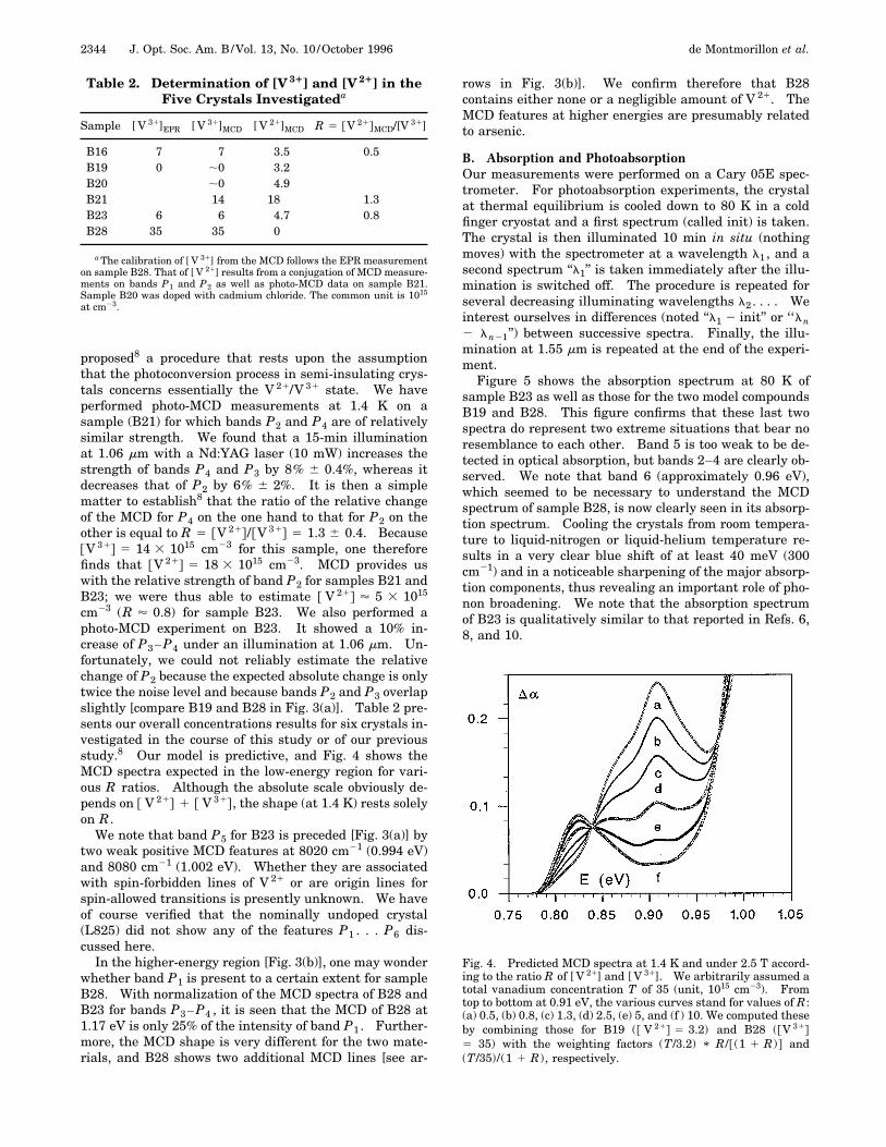
proposed8 a procedure that rests upon the assumptionthat the photoconversion process in semi-insulating crys-tals concerns essentially the V 21/V 31 state. We haveperformed photo-MCD measurements at 1.4 K on asample (B21) for which bands P2 and P4 are of relativelysimilar strength. We found that a 15-min illuminationat 1.06 mm with a Nd:YAG laser (10 mW) increases thestrength of bands P4 and P3 by 8% 6 0.4%, whereas itdecreases that of P2 by 6% 6 2%. It is then a simplematter to establish8 that the ratio of the relative changeof the MCD for P4 on the one hand to that for P2 on theother is equal to R 5 @V 21#/@V 31# 5 1.3 6 0.4. Because@V 31# 5 14 3 1015 cm23 for this sample, one thereforefinds that @V 21# 5 18 3 1015 cm23. MCD provides uswith the relative strength of band P2 for samples B21 andB23; we were thus able to estimate @ V 21# ' 5 3 1015
cm23 (R ' 0.8) for sample B23. We also performed aphoto-MCD experiment on B23. It showed a 10% in-crease of P3–P4 under an illumination at 1.06 mm. Un-fortunately, we could not reliably estimate the relativechange of P2 because the expected absolute change is onlytwice the noise level and because bands P2 and P3 overlapslightly [compare B19 and B28 in Fig. 3(a)]. Table 2 pre-sents our overall concentrations results for six crystals in-vestigated in the course of this study or of our previousstudy.8 Our model is predictive, and Fig. 4 shows theMCD spectra expected in the low-energy region for vari-ous R ratios. Although the absolute scale obviously de-pends on @ V 21# 1 @ V 31#, the shape (at 1.4 K) rests solelyon R.We note that band P5 for B23 is preceded [Fig. 3(a)] by
two weak positive MCD features at 8020 cm21 (0.994 eV)and 8080 cm21 (1.002 eV). Whether they are associatedwith spin-forbidden lines of V 21 or are origin lines forspin-allowed transitions is presently unknown. We haveof course verified that the nominally undoped crystal(L825) did not show any of the features P1 . . . P6 dis-cussed here.In the higher-energy region [Fig. 3(b)], one may wonder
whether band P1 is present to a certain extent for sampleB28. With normalization of the MCD spectra of B28 andB23 for bands P3–P4 , it is seen that the MCD of B28 at1.17 eV is only 25% of the intensity of band P1 . Further-more, the MCD shape is very different for the two mate-rials, and B28 shows two additional MCD lines [see ar-
Table 2. Determination of [V 31] and [V 21] in theFive Crystals Investigateda
Sample [ V 31]EPR [ V 31]MCD [ V 21]MCD R 5 @V 21#MCD/[V31]
B16 7 7 3.5 0.5B19 0 ;0 3.2B20 ;0 4.9B21 14 18 1.3B23 6 6 4.7 0.8B28 35 35 0
aThe calibration of [ V 31] from the MCD follows the EPR measurementon sample B28. That of [ V 21] results from a conjugation of MCD measure-ments on bands P1 and P2 as well as photo-MCD data on sample B21.Sample B20 was doped with cadmium chloride. The common unit is 1015
at cm23.
rows in Fig. 3(b)]. We confirm therefore that B28contains either none or a negligible amount of V 21. TheMCD features at higher energies are presumably relatedto arsenic.
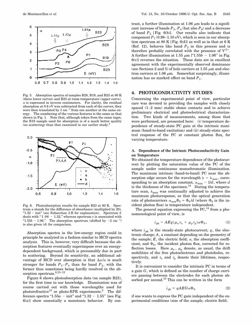
B. Absorption and PhotoabsorptionOur measurements were performed on a Cary 05E spec-trometer. For photoabsorption experiments, the crystalat thermal equilibrium is cooled down to 80 K in a coldfinger cryostat and a first spectrum (called init) is taken.The crystal is then illuminated 10 min in situ (nothingmoves) with the spectrometer at a wavelength l1 , and asecond spectrum ‘‘l1’’ is taken immediately after the illu-mination is switched off. The procedure is repeated forseveral decreasing illuminating wavelengths l2 . . . . Weinterest ourselves in differences (noted ‘‘l1 2 init’’ or ‘ ‘ln2 ln21’’) between successive spectra. Finally, the illu-mination at 1.55 mm is repeated at the end of the experi-ment.Figure 5 shows the absorption spectrum at 80 K of
sample B23 as well as those for the two model compoundsB19 and B28. This figure confirms that these last twospectra do represent two extreme situations that bear noresemblance to each other. Band 5 is too weak to be de-tected in optical absorption, but bands 2–4 are clearly ob-served. We note that band 6 (approximately 0.96 eV),which seemed to be necessary to understand the MCDspectrum of sample B28, is now clearly seen in its absorp-tion spectrum. Cooling the crystals from room tempera-ture to liquid-nitrogen or liquid-helium temperature re-sults in a very clear blue shift of at least 40 meV (300cm21) and in a noticeable sharpening of the major absorp-tion components, thus revealing an important role of pho-non broadening. We note that the absorption spectrumof B23 is qualitatively similar to that reported in Refs. 6,8, and 10.
Fig. 4. Predicted MCD spectra at 1.4 K and under 2.5 T accord-ing to the ratio R of [ V 21] and [ V 31]. We arbitrarily assumed atotal vanadium concentration T of 35 (unit, 1015 cm23). Fromtop to bottom at 0.91 eV, the various curves stand for values of R:(a) 0.5, (b) 0.8, (c) 1.3, (d) 2.5, (e) 5, and (f ) 10. We computed theseby combining those for B19 (@ V 21# 5 3.2) and B28 (@V 31#5 35) with the weighting factors (T/3.2) * R/@(1 1 R)# and(T/35)/(1 1 R), respectively.
de Montmorillon et al. Vol. 13, No. 10 /October 1996 /J. Opt. Soc. Am. B 2345
Absorption spectra in the low-energy region could inprinciple be analyzed in a fashion similar to MCD spectraanalysis. This is, however, very difficult because the ab-sorption features eventually superimpose over an energy-dependent background, which is presumably due in partto scattering. Beyond its sensitivity, an additional ad-vantage of MCD over absorption is that Da /a is muchstronger for bands P3–P4 than for band P2 , with theformer thus sometimes being hardly resolved in the ab-sorption spectrum.6,10–12
Figure 6 shows photoabsorption data (on sample B23),for the first time to our knowledge. Illumination was ofcourse carried out with those wavelengths used forphotorefractive13 or photo-EPR experiments.2 The dif-ference spectra ‘‘1.55a 2 init’’ and ‘‘1.32 2 1.55’’ [see Fig.6(a)] show essentially a monotonic behavior. By con-
Fig. 5. Absorption spectra of samples B28, B19, and B23 at 80 K(three lower curves) and B23 at room temperature (upper curve).a is expressed in inverse centimeters. For clarity, the residualabsorption at 0.6 eV was subtracted from each of the curves; theywere then translated by 1 cm21 from one another at the same en-ergy. The numbering of the various features is the same as thatshown in Fig. 1. Note that, although taken from the same ingot,the B19 sample used for absorption is of a much better quality(no scattering) than that examined in our earlier study.8
Fig. 6. Photoabsorption results for sample B23 at 80 K. Spec-trum a stands for the difference of absorbance (multiplied by 20),‘‘1.32 2 init’’ (see Subsection 3.B for explanation). Spectrum bdeals with ‘‘1.06 2 1.32,’’ whereas spectrum c is associated with‘‘1.55b 2 1.06.’’ The absorption spectrum (shifted by 22 cm21)is also given (d) for comparison.
trast, a further illumination at 1.06 mm leads to a signifi-cant increase of bands P3 , P4 (but also P6) and a decreaseof band P2 [ Fig. 6(b)]. Our results also indicate thatcomponent P7 (0.98–1.10 eV), which is seen in our absorp-tion spectrum at 80 K [Fig. 6(d)] as well as in that at 6 K(Ref. 12), behaves like band P2 in this process and istherefore probably correlated with the presence of V 21.A further illumination at 1.55 mm [‘‘1.55b 2 1.06’’ in Fig.6(c)] reverses the situation. These data are in excellentagreement with the experimentally observed dominance(see Sections 2 and 5) of hole carriers at 1.55 mm and elec-tron carriers at 1.06 mm. Somewhat surprisingly, illumi-nation has no marked effect on band P1 .
4. PHOTOCONDUCTIVITY STUDIESConcerning the experimental point of view, particularcare was devoted to providing the samples with closelyspaced (1–2 mm) stable ohmic contacts and to achievepreliminary electrical and photoelectrical characteriza-tion. Two kinds of measurements, among those thatwere performed, are presented here: (i) temperature de-pendence of steady-state PC gain at the intrinsic maxi-mum (band-to-band excitation) and (ii) steady-state spec-tral response of the PC at constant photon flux, forvarying temperature.
A. Dependence of the Intrinsic Photoconductivity Gainon TemperatureWe obtained the temperature dependence of the photocur-rent by plotting the saturation value of the PC of thesample under continuous monochromatic illumination.The maximum intrinsic (band-to-band) PC near the ab-sorption edge occurs for the wavelength l 5 lmax , corre-sponding to an absorption constant, amax ; 1/d, where dis the thickness of the specimen.14 During the tempera-ture scan, lmax was continually adjusted to achieve themaximum photoresponse, so that the optical generationrate of photocarriers amaxF0 5 F0 /d (where F0 is the in-cident photon flux) is temperature independent.The general equation expressing the PC,14 from a phe-
nomenological point of view, is
iph 5 AEq~mntn 1 mptp!aF0 , (1)
where iph is the steady-state photocurrent; q, the elec-tronic charge; A, a constant depending on the geometry ofthe sample; E, the electric field; a, the absorption coeffi-cient; and F0 , the incident photon flux, corrected for re-flection losses. Here mn , mp denote, as usual, the driftmobilities of the free photoelectrons and photoholes, re-spectively, and tn and tp denote their lifetimes, respec-tively.It is convenient to consider the intrinsic PC in terms of
a gain G, which is defined as the number of charge carri-ers passing between the electrodes for each photon ab-sorbed per second.15 This can be written in the form
iph 5 qAEGaF0 (2)
if one wants to express the PC gain independent of the ex-perimental conditions (size of the sample, electric field).
2346 J. Opt. Soc. Am. B/Vol. 13, No. 10 /October 1996 de Montmorillon et al.
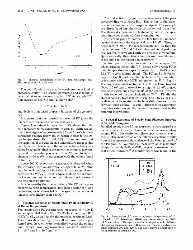
The gain G, which can also be considered as a kind ofphotosensitivity,15 is a crucial parameter and is found tobe equal, at room temperature, to ;0.35 for sample B23.Comparison of Eqs. (1) and (2) shows that
G 5 mntn 1 mptp (3)
and depicts a material property in terms of the mt prod-uct.It appears that the thermal variation of PC gives the
temperature dependence of the product mt.Figure 7, obtained for specimen B23, shows that the
gain increases fairly exponentially with 1/T (with two ac-tivation energies of approximately 20 and 5 meV) for mea-surements roughly below 180 K, which is close to the De-bye temperature [158 K (Ref. 16)]. If one assumes thatthe variation of the gain in this temperature range is duemainly to the lifetime; with that of the mobility being con-sidered negligible, then these activation energies may cor-respond to acoustic phonons (;5 meV) and to opticalphonons (;20 meV), in agreement with the values foundin Ref. 17.Above 200 K, in contrast, a decrease is observed when
1/T increases, with an activation energy of 63 meV. Thismay be explained by the fact that in this range of tem-perature the V 21/V 31 levels empty, making the recombi-nation centers less active and permitting the increase ofthe free-electron lifetime.It is noteworthy that the variation of the PC gain varies
moderately with temperature, less than a factor of 4, andmodulates, as is shown below, the spectral responses attemperatures higher than 180 K.
B. Spectral Response of Steady-State Photoconductivityat Room TemperatureThe steady-state PC spectra were measured at ;300 Kfor samples B23 (CdTe:V), B28 (CdTe:V, As), and B19(CdTe:V, Cl), as well as for the undoped specimen L825.The curves shown in Fig. 8, as well as those that are pre-sented from here on, were normalized versus the photonflux, which was approximately constant (between5 3 1012 and 3 3 1013 cm22 s21).
Fig. 7. Thermal dependence of the PC gain for sample B23.The ordinate unit is arbitrary.
The first noteworthy point is the sharpness of the peakcorresponding to intrinsic PC. This is due to the steep-ness of the fundamental absorption edge of CdTe owing tothe direct band-gap character of the optical transition.The strong decrease on the high-energy side of the spec-trum indicates strong surface recombination.The second point to note is the fact that the undoped
crystal shows only the sharp peak at ;1.5 eV. Thus, in-dependent of MCD, PC measurements tell us that thebands between 0.7 and 1.4 eV, observed for doped crys-tals, are really correlated with the presence of vanadium.Quite naturally, these bands bear a close resemblance tothose found in the absorption spectra.3,6,18
A final point, of great interest, is that sample B19,which contains essentially V 21, shows only a weak PC atroom temperature in a spectral region (at ;0.8 eV), whereB28 (V 31) gives a large signal. The PC band at lower en-ergies in Fig. 8 must therefore be labeled P3 to maintainconsistency with our MCD assignment to V 31 (Fig. 3).The largest contribution to the PC of B19 is found to occurabove 1.0 eV and to extend to as high as 1.4 eV, in goodagreement with our assignment8 of the spectral featuresin this region to the photoionization of V 21. Finally, theshift of band P3 from 0.82 eV in Fig. 8 to 0.87 eV in Fig. 3is thought to be related to the blue shift observed in ab-sorption upon cooling. A small difference in calibrationmay also exist among the monochromators used in thedifferent laboratories.
C. Spectral Response of Steady-State Photoconductivityat Variable TemperatureDetailed steady-state PC measurements were carried outfor a series of temperatures on the semi-insulatingsample B23. For clarity only three spectra are shown inFig. 9. The modification of the intrinsic spectrum resultsfrom the temperature dependence of the band gap and ofthe PC gain G. We found a linear shift of its maximumof approximately 0.46 meV/K, in good agreement withthat of the literature.19 A similar figure was found in the
Fig. 8. Steady-state PC spectra at room temperature of Cl-codoped (B19), As-codoped (B28), and semi-insulating (B23)CdTe:V crystals. The spectrum of an undoped sample (L825) isalso shown for comparison. Because the various spectra weretaken between 290 and 320 K, one can observe a slight shift ofthe maximum of intrinsic PC.
de Montmorillon et al. Vol. 13, No. 10 /October 1996 /J. Opt. Soc. Am. B 2347
course of similar measurements on other samples. Com-parison of spectrum labeled 320 K with that of B23 of Fig.8, obtained at 294 K, shows that the shift in energy of themaximum, of approximately 10 meV, indeed correspondsto that predicted by the law just mentioned. For energieshigher than the band gap we can observe that the surfacerecombination is less important at 320 K than at roomtemperature. Here also, the magnitude of the maximumfollows the temperature dependence of G, shown in Fig. 7.G is minimum at 200 K and is about 2 times higher atroom and liquid-nitrogen temperatures, in agreementwith our previous findings.As for the temperature dependence of the extrinsic part
in the most interesting low-energy region, the labeling ofthe resolved features follows that used for MCD (Fig. 3)and absorption (Figs. 5 and 6). The decrease of theirmagnitude between 320 and 200 K follows roughly that ofthe gain. Below 200 K, however, the change is drastic,and band P3 has almost vanished at 81 K. Its width doesnot appear to vary significantly, and its height was foundto follow exp(2W/kBT), withW ' 30 meV. Band P3 alsosuffers a clearly observable linear energy shift of 0.23meV/K, i.e., exactly half that of the band gap. In contrastwith the above results, the positions of bands P7 and P4(Fig. 9) are temperature independent. At 81 K, band P4occurs as a weak shoulder between P3 and P7 .
5. PHOTOREFRACTIVE MEASUREMENTSA. Experimental ArrangementPhotorefractive performances of sample B23 are analyzedin a two-beam-coupling experiment. The measurementof the strength of the photorefractive energy transfer gainfrom a pump beam toward a probe beam (from which wededuce the photorefractive gain G) as a function of thegrating spacing provides two important parameters of thephotorefractive effect: the electron–hole competition co-efficient j0 , and the inverse of the Debye screening lengthk0 (i.e., the effective trap density Neff).
20 The expressionof the gain with the grating spacing L (or grating wavenumber k 5 2p/L), when one considers that theelectron–hole competition factor is independent of the
Fig. 9. Temperature dependence of the normalized steady-statePC for sample B23. Note that PC for E > 1.35 eV was dividedby 5 so as to magnify the low-energy and highly structured sec-tions.
grating spacing, as is usually assumed in semiconductors,is21,22
G 52pn0
3reffl cos u
kBTe
j0k
1 1 ~k2/k02!, (4)
with k02 5 @e2/(«kBT)#Neff . u is the half-angle between
the beams inside the crystal; n0 , the linear refractive in-dex of the material; reff , the effective electro-optic coeffi-cient that depends on the crystal and the beam polariza-tion orientations;23 and «, the dielectric constant. Allthese parameters are known from the literature.The two experimentally determined parameters (j0 and
Neff) depend on the deep-level characteristics through thewell-known expressions22
Neff 5@V 21#@V 31#
@V 21# 1 @V 31#, j0 5
Sn@V 21# 2 Sp@V 31#
Sn@V 21# 1 Sp@V 31#,
to which we add the linear absorption of the crystals a5 Sn@V 21# 1 Sp@V 31#. We consider here the opticalgeneration of electrons and holes from V21 and V 31, re-spectively, with photoionization cross sections Sn and Sp .The measurements are performed at the three wave-
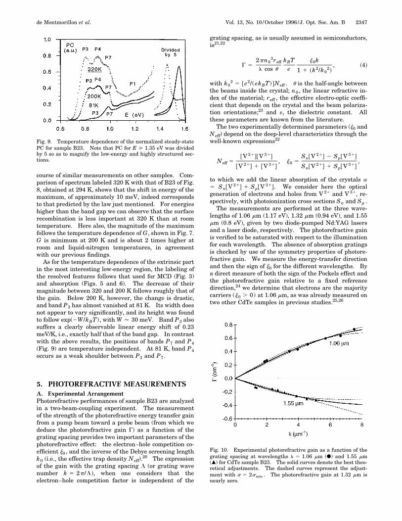
lengths of 1.06 mm (1.17 eV), 1.32 mm (0.94 eV), and 1.55mm (0.8 eV), given by two diode-pumped Nd:YAG lasersand a laser diode, respectively. The photorefractive gainis verified to be saturated with respect to the illuminationfor each wavelength. The absence of absorption gratingsis checked by use of the symmetry properties of photore-fractive gain. We measure the energy-transfer directionand then the sign of j0 for the different wavelengths. Bya direct measure of both the sign of the Pockels effect andthe photorefractive gain relative to a fixed referencedirection,24 we determine that electrons are the majoritycarriers (j0 . 0) at 1.06 mm, as was already measured ontwo other CdTe samples in previous studies.25,26
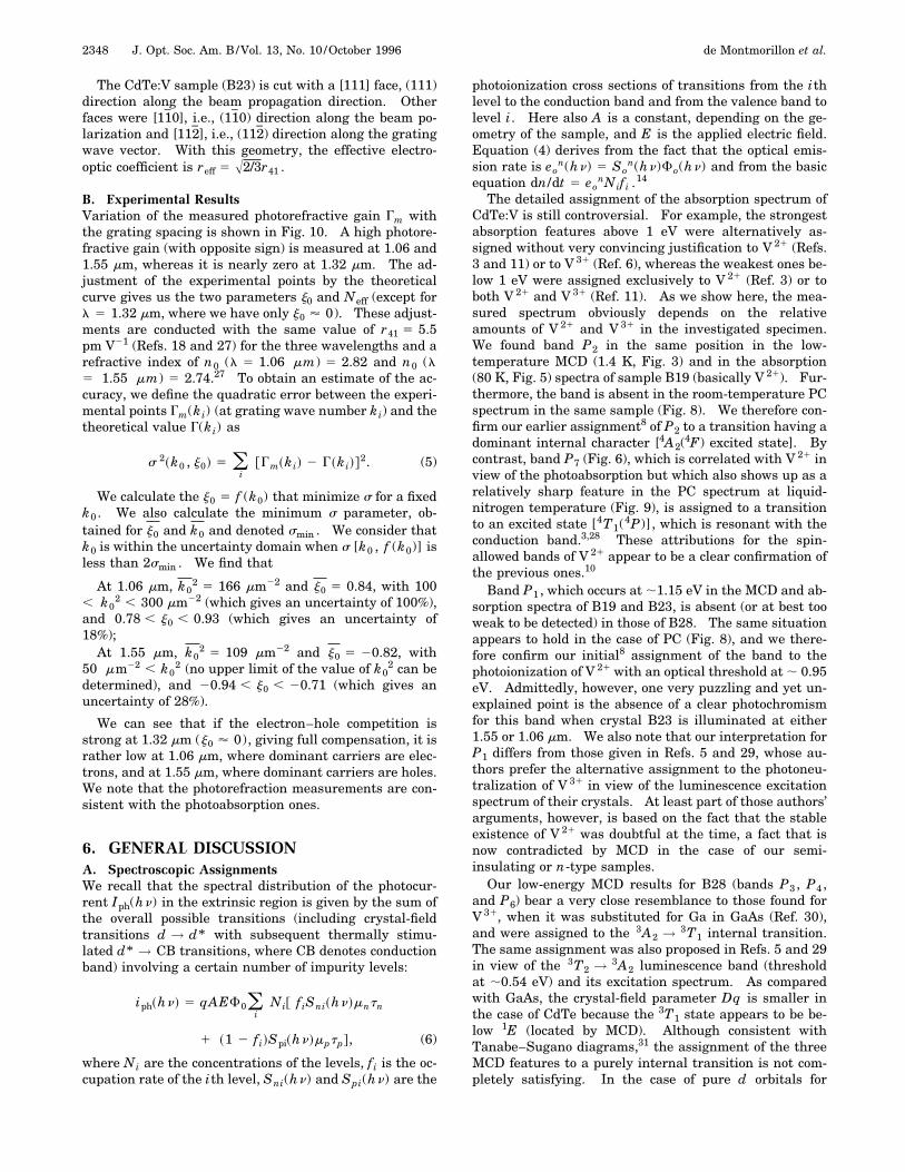
Fig. 10. Experimental photorefractive gain as a function of thegrating spacing at wavelengths l 5 1.06 mm (d) and 1.55 mm(m) for CdTe sample B23. The solid curves denote the best theo-retical adjustments. The dashed curves represent the adjust-ment with s 5 2smin . The photorefractive gain at 1.32 mm isnearly zero.
2348 J. Opt. Soc. Am. B/Vol. 13, No. 10 /October 1996 de Montmorillon et al.
The CdTe:V sample (B23) is cut with a [111] face, (111)direction along the beam propagation direction. Otherfaces were [110], i.e., (110) direction along the beam po-larization and [112], i.e., (112) direction along the gratingwave vector. With this geometry, the effective electro-optic coefficient is reff 5 A2/3r41 .
B. Experimental ResultsVariation of the measured photorefractive gain Gm withthe grating spacing is shown in Fig. 10. A high photore-fractive gain (with opposite sign) is measured at 1.06 and1.55 mm, whereas it is nearly zero at 1.32 mm. The ad-justment of the experimental points by the theoreticalcurve gives us the two parameters j0 and Neff (except forl 5 1.32 mm, where we have only j0 ' 0). These adjust-ments are conducted with the same value of r41 5 5.5pm V21 (Refs. 18 and 27) for the three wavelengths and arefractive index of n0 (l 5 1.06 mm) 5 2.82 and n0 (l5 1.55 mm) 5 2.74.27 To obtain an estimate of the ac-curacy, we define the quadratic error between the experi-mental points Gm(ki) (at grating wave number ki) and thetheoretical value G(ki) as
s 2~k0 , j0! 5 (i
@Gm~ki! 2 G~ki!#2. (5)
We calculate the j0 5 f (k0) that minimize s for a fixedk0 . We also calculate the minimum s parameter, ob-tained for j0 and k0 and denoted smin . We consider thatk0 is within the uncertainty domain when s [k0 , f (k0)] isless than 2smin . We find that
At 1.06 mm, k02 5 166 mm22 and j0 5 0.84, with 100
, k02 , 300 mm22 (which gives an uncertainty of 100%),
and 0.78 , j0 , 0.93 (which gives an uncertainty of18%);At 1.55 mm, k0
2 5 109 mm22 and j0 5 20.82, with50 mm22 , k0
2 (no upper limit of the value of k02 can be
determined), and 20.94 , j0 , 20.71 (which gives anuncertainty of 28%).
We can see that if the electron–hole competition isstrong at 1.32 mm (j0 ' 0), giving full compensation, it israther low at 1.06 mm, where dominant carriers are elec-trons, and at 1.55 mm, where dominant carriers are holes.We note that the photorefraction measurements are con-sistent with the photoabsorption ones.
6. GENERAL DISCUSSIONA. Spectroscopic AssignmentsWe recall that the spectral distribution of the photocur-rent Iph(hn) in the extrinsic region is given by the sum ofthe overall possible transitions (including crystal-fieldtransitions d → d* with subsequent thermally stimu-lated d* → CB transitions, where CB denotes conductionband) involving a certain number of impurity levels:
iph~hn! 5 qAEF0(iNi@ fiSni~hn!mntn
1 ~1 2 fi!Spi~hn!mptp#, (6)
where Ni are the concentrations of the levels, fi is the oc-cupation rate of the ith level, Sni(hn) and Spi(hn) are the
photoionization cross sections of transitions from the ithlevel to the conduction band and from the valence band tolevel i. Here also A is a constant, depending on the ge-ometry of the sample, and E is the applied electric field.Equation (4) derives from the fact that the optical emis-sion rate is eo
n(hn) 5 Son(hn)Fo(hn) and from the basic
equation dn/dt 5 eonNifi .
14
The detailed assignment of the absorption spectrum ofCdTe:V is still controversial. For example, the strongestabsorption features above 1 eV were alternatively as-signed without very convincing justification to V 21 (Refs.3 and 11) or to V 31 (Ref. 6), whereas the weakest ones be-low 1 eV were assigned exclusively to V 21 (Ref. 3) or toboth V 21 and V 31 (Ref. 11). As we show here, the mea-sured spectrum obviously depends on the relativeamounts of V 21 and V 31 in the investigated specimen.We found band P2 in the same position in the low-temperature MCD (1.4 K, Fig. 3) and in the absorption(80 K, Fig. 5) spectra of sample B19 (basically V 21). Fur-thermore, the band is absent in the room-temperature PCspectrum in the same sample (Fig. 8). We therefore con-firm our earlier assignment8 of P2 to a transition having adominant internal character [4A2(
4F) excited state]. Bycontrast, band P7 (Fig. 6), which is correlated with V
21 inview of the photoabsorption but which also shows up as arelatively sharp feature in the PC spectrum at liquid-nitrogen temperature (Fig. 9), is assigned to a transitionto an excited state [4T1(
4P)], which is resonant with theconduction band.3,28 These attributions for the spin-allowed bands of V 21 appear to be a clear confirmation ofthe previous ones.10
Band P1 , which occurs at ;1.15 eV in the MCD and ab-sorption spectra of B19 and B23, is absent (or at best tooweak to be detected) in those of B28. The same situationappears to hold in the case of PC (Fig. 8), and we there-fore confirm our initial8 assignment of the band to thephotoionization of V 21 with an optical threshold at ; 0.95eV. Admittedly, however, one very puzzling and yet un-explained point is the absence of a clear photochromismfor this band when crystal B23 is illuminated at either1.55 or 1.06 mm. We also note that our interpretation forP1 differs from those given in Refs. 5 and 29, whose au-thors prefer the alternative assignment to the photoneu-tralization of V 31 in view of the luminescence excitationspectrum of their crystals. At least part of those authors’arguments, however, is based on the fact that the stableexistence of V 21 was doubtful at the time, a fact that isnow contradicted by MCD in the case of our semi-insulating or n-type samples.Our low-energy MCD results for B28 (bands P3 , P4 ,
and P6) bear a very close resemblance to those found forV 31, when it was substituted for Ga in GaAs (Ref. 30),and were assigned to the 3A2 → 3T1 internal transition.The same assignment was also proposed in Refs. 5 and 29in view of the 3T2 → 3A2 luminescence band (thresholdat ;0.54 eV) and its excitation spectrum. As comparedwith GaAs, the crystal-field parameter Dq is smaller inthe case of CdTe because the 3T1 state appears to be be-low 1E (located by MCD). Although consistent withTanabe–Sugano diagrams,31 the assignment of the threeMCD features to a purely internal transition is not com-pletely satisfying. In the case of pure d orbitals for
de Montmorillon et al. Vol. 13, No. 10 /October 1996 /J. Opt. Soc. Am. B 2349
the d2 configuration, theory predicts32 a negative MCDfor the spin-forbidden line (as observed) and an S-shapedMCD (due to spin-orbit coupling) for the spin-allowedtransition. This is indeed the situation that results forthe isoelectronic d2 ions Mn51 (Ref. 32) and Ti21 (Ref. 6)in tetrahedral symmetry. At this stage, we stress thatthe considered internal transition corresponds to a trans-fer of an electron from the vanadiumlike e orbital to the t2orbital, which strongly hybridizes with the host. Theligand–field picture is therefore not fully appropriate.An explanation of the different behavior of V 31 and Ti21
requires theoretical research.The blue shift (half that of the band gap) of P3 under
cooling implies its assignment to the VB → d2 charge-transfer process where VB denotes valence band. Thecomplex temperature dependence of PC, however, is notyet understood.In summary, the occurrence of two complementary pro-
cesses in the P3–P6 region are proposed: (i) photoneu-tralization of V 31 leading to hole conductivity and (ii)crystal-field transition (3A2 → 3T1) of V
31, with subse-quent thermally stimulated 3T1 ↔ CB transfers (electronconductivity).
B. Photoionization Cross SectionsThe insertion of vanadium in CdTe creates a deep levelthat corresponds to the two charge states V 21/V 31.These two charge states are responsible for the absorp-tion and, as shown in the PC measurements, for the pho-togeneration of charge carriers at room temperature.The latter condition is a necessary one if the defect is tobe the source of the photorefractive effect. The concen-tration in the two vanadium species is given by the EPRexperiment and by the MCD measurements described inSections 2 and 3. The EPR experiment gives us @V 31#' 6 3 1015 cm23, whereas the MCD allows us to deter-mine @V 21# ' 5 3 1015 cm23 (Table 2).The use of these two values gives, for the effective trap
density, Neff ' 2.7 3 1015 cm23, from which we deducek0
2 ' 200 mm22, which corresponds to the experimentalvalues.Now, from j0 and considering that the value of the ab-
sorption a (Fig. 5), corrected from a constant backgroundabsorption, is due only to a process that creates electronsand holes from a single defect under two charge states(V 21/V 31 here), we deduce the two products an5 Sn@V 21# and ap 5 Sp@V 31# for each wavelength [us-ing an 5 (a/2)(1 1 j0) and ap 5 (a/2)(1 2 j0)]. Thesevalues, together with the concentrations given in Table 2above, allow us to calculate the photoionization cross sec-tions. The ratio of electron and hole absorptions(an /ap), and thus the ratio of the photoionization crosssection, is given by the electron–hole competition coeffi-cient only, whereas the absolute value of cross sections isdetermined by the value of the absorption a of the crystal.We then deduce the following:
At 1.06 mm: (a 5 1.6 cm21), Sn ' 2.9 3 10216 cm2, Sp' 2.2 3 10217 cm2;At 1.32 mm: (a 5 0.85 cm21), Sn ' 8.6 3 10217 cm2,
Sp ' 7.2 3 10217 cm2;
At 1.55 mm: (a 5 0.58 cm21), Sn ' 1.1 3 10217 cm2,Sp ' 8.8 3 10217 cm2.
The trends of these results correspond to the ones previ-ously published.33 We have a monotonic decrease of Snwith increasing wavelength, whereas Sp shows a maxi-mum in the 1.3–1.5-mm region of the spectra, as alreadyobserved. The orders of magnitude for these cross sec-tions are also kept, compared with the ones given in Ref.33. The assumption that we use in our interpretation ofthe experimental results, that all of the absorption con-tributes to charge generation, is perhaps not totally war-ranted because of inadequate correction of the back-ground or because of the presence of internal transitions.For example, our experimental data were processed as-suming a constant background of absorption (consideringthe crystal absorption to be zero at l 5 2 mm) for ease ofuse. Nevertheless, even if this assumption is not totallywarranted, the results remain qualitatively the same;only the exact values of cross sections vary, and the fea-tures and the ratio of the photoionization cross sectionsremain the same.
7. CONCLUSIONIn summary, we have performed a large number of spec-troscopic experiments as well as photorefractive measure-ments in CdTe:V crystals with the goal of identifying thedefect responsible for the photorefractive effect. We haveextended earlier MCD studies and have further illus-trated the use of the technique to monitor [V 21] and[V 31] simultaneously. Photoabsorption results are re-ported, for the first time to our knowledge. They confirmMCD and photo-MCD assignments. Furthermore, theyindicate the existence of new features at ;0.95 eV (bandP6 , V
31 related) and 1 eV (band P7 , V21 related).
The spectral response of the steady-state PC of CdTe:Vhas been determined for n-type (Cl-doped), p-type (As-doped), and semi-insulating (sample B23) V-doped crys-tals and has been compared with that of an undoped one.These results confirm that vanadium is indeed the domi-nant carrier donor. They are consistent with MCD,which shows no noticeable feature for the undopedsample. Most of the bands found in MCD and absorption(except P2) were found to be responsible for the genera-tion of free carriers, a necessary condition for them tohave an influence on the photorefractive effect. The ther-mal dependence of PC has also been measured for sampleB23. The position of the various bands at 81 K correlateswell with MCD (1.4 K) and absorption (80 K) results. Al-though their temperature dependence (shift, intensity) isnot fully understood, it indicates that internal (d → d* )transitions are presumably followed by a subsequentthermally stimulated d* → CB transfer.The semi-insulating CdTe sample B23 has also been
the object of a detailed photorefractive investigation. Itdemonstrates the predominance of hole carriers at 1.55mm and electron carriers at 1.06 mm, in excellent agree-ment with the photoabsorption results. Electron–holecompetition is very strong at 1.32 mm, leading to a com-plete cancellation of j0 (corresponding to equal generation
2350 J. Opt. Soc. Am. B/Vol. 13, No. 10 /October 1996 de Montmorillon et al.
of electrons and holes, an 5 ap). The measured effectivetrap density was found to be in accord with the [V 21] andthe [ V 31] concentrations determined by MCD and EPR.Using the measured room-temperature absorption coeffi-cient at each wavelength and the [ V 21] and the [V 31]concentrations determined by MCD and EPR, we havealso estimated the associated photoionization cross sec-tions at the three studied wavelengths and have foundthem to be consistent with those published previously.Moreover, the self-consistency of our results gives verystrong support to the correctness of our concentration de-terminations.In sum, although it is well established that CdTe crys-
tals may contain a large variety of defects,34 it appearsthat most of our present physical results can be under-stood under the assumption that the photoconversion pro-cesses in V-doped crystals predominantly concern theV 21/V 31 state. A few experimental facts remain unex-plained. This condition applies, in particular, to the ab-sence of a clear change of the absorption above 1 eV forour semi-insulating crystal when it was submitted to anillumination at 1.55 or 1.06 mm. This suggests compet-ing processes and requires additional research. It fol-lows from earlier theoretical considerations35,36 andrecent37 experimental studies on ZnTe:V that the exist-ence of the acceptor level V 21/V1 relatively close ('0.4eV) to the conduction band cannot be completely ruledout.
ACKNOWLEDGMENTSSupport for this research by Direction des RecherchesEtudes et Techniques (grant number 94-063) is gratefullyacknowledged. We are also indebted to one of the refer-ees for his very stimulating criticism of our manuscript.
REFERENCES1. Ph. Delaye, L. A. de Montmorillon, H. J. von Bardeleben,
and G. Roosen, ‘‘Photorefractive wave mixing in undopedliquid encapsulated Czochralski GaAs at 1.5 mm: valida-tion of photorefractive modeling,’’ Appl. Phys. Lett. 64, 2640(1994).
2. H. J. von Bardeleben, J. C. Launay, and V. Mazoyer, ‘‘De-fects in photorefractive CdTe:V: an electron paramagneticresonance study,’’ Appl. Phys. Lett. 63, 1140 (1993).
3. R. Schwartz, M. Ziari, and S. Trivedi, ‘‘Electron paramag-netic resonance and an optical investigation of photorefrac-tive vanadium-doped CdTe,’’ Phys. Rev. B 49, 5274 (1994).
4. H. J. von Bardeleben, V. Mazoyer, X. Launay, and J. C.Launay, ‘‘A comparative electron paramagnetic resonancestudy of vanadium in n-type, semi-insulating and p-typeCdTe,’’ Semicond. Sci. Technol. 10, 163 (1995).
5. H. J. Schultz and J. Kreissl, ‘‘Optical and EPR properties ofV and Ti ions in CdTe,’’ Opt. Mater. 4, 202 (1995).
6. P. Christmann, H. C. Alt, D. M. Hofmann, B. K. Meyer, J.Kreissl, R. Schwarz, and K. W. Benz, ‘‘Optically detectedmagnetic resonance investigations on titanium and vana-dium ions in CdTe,’’ Opt. Mater. 4, 210 (1995).
7. B. Lambert, M. Gauneau, G. Grandpierre, M. Schoisswohl,H. J. von Bardeleben, J. C. Launay, V. Mazoyer, A. Aoudia,E. Rzepka, Y. Marfaing, and R. Triboulet, ‘‘Effective trapconcentration in photorefractive CdTe:V and ZnCdTe:Vcrystals,’’ Opt. Mater. 4, 265 (1995).
8. B. Briat, F. Ramaz, A. Hamri, H. J. von Bardeleben, J. C.
Launay, and V. Mazoyer, ‘‘Monitoring of V 21 and V 31 invanadium-doped CdTe: a combined magnetic circular di-chroism and electron paramagnetic resonance approach,’’Semicond. Sci. Technol. 10, 1629 (1995).
9. H. J. von Bardeleben, C. Miesner, J. Monge, B. Briat, J. C.Launay, and X. Launay, ‘‘An electron paramagnetic reso-nance and magneto-optical study of vanadium inZnxCd12xTe:V,’’ Semicond. Sci. Technol. 10, 1 (1995).
10. P. A. Slodowy and J. M. Baranowski, ‘‘Absorption spectra ofTi(d2), V(d3), and Cr(d4) ions in CdTe,’’ Phys. Status SolidiB 49, 499 (1972).
11. A. Aoudia, E. Rzepka, A. Lusson, A. Thomson-Carli, D.Schneider, Y. Marfaing, and R. Triboulet, ‘‘Crystal growthand characterization of CdTe doped with transition metalelements,’’ Opt. Mater. 4, 241 (1995).
12. E. Rzepka, Y. Marfaing, M. Cuniot, and R. Triboulet, ‘‘Deepcentres for optical processing in CdTe,’’ Mater. Sci. Eng. B16, 262 (1993).
13. L. A. de Montmorillon, Ph. Delaye, J. C. Launay, and G.Roosen, ‘‘Comparative study of CdTe and GaAs photorefrac-tive performances from 1 mm to 1.55 mm,’’ Opt. Mater. 4,233 (1995).
14. J. P. Zielinger and M. Tapiero, ‘‘Assessment of deep levelsin photorefractive materials by transient photoelectricmethods,’’ J. Phys. (Paris) III 3, 1327 (1993).
15. R. H. Bube, Electronic Properties of Crystalline Solids (Aca-demic, New York, 1974).
16. J. Jouglar, C. Hetroit, P. L. Vuillermoz, and R. Triboulet,‘‘Influence of growth parameters on CdTe low temperaturethermal conductivity,’’ J. Appl. Phys. 51, 3171 (1980).
17. M. S. Kushwaha and S. S. Kushwaha, ‘‘Lattice dynamics ofZnTe, CdTe, GaP, and InP,’’ Can. J. Phys. 58, 351 (1980).
18. A. Partovi, J. Millerd, E. M. Garmire, M. Ziari, W. H.Steier, S. B. Trivedi, and M. B. Klein, ‘‘Photorefractivity at1.5 mm in CdTe:V,’’ Appl. Phys. Lett. 57, 846 (1990).
19. A. Muranevich, M. Roitberg, and E. Finkman, ‘‘Growth ofCdTe single crystals,’’ J. Cryst. Growth 64, 285 (1983).
20. M. B. Klein and G. C. Valley, ‘‘Beam coupling in BaTiO3 at442 nm,’’ J. Appl. Phys. 57, 4901 (1985).
21. N. V. Kukhtarev, V. B. Markov, S. G. Odulov, M. S. Soskin,and V. L. Vinetskii, ‘‘Holographic storage in electroopticcrystals. I. Steady state,’’ Ferroelectrics 22, 949 (1979); ‘‘Ho-lographic storage in electrooptic crystals. II. Beamcoupling–light amplification,’’ 22, 961 (1979).
22. F. P. Strohkendl, J. M. C. Jonathan, and R. W. Hellwarth,‘‘Hole–electron competition in photorefractive gratings,’’Opt. Lett. 11, 312 (1986).
23. J. C. Fabre, J. M. C. Jonathan, and G. Roosen, ‘‘43m pho-torefractive materials in energy transfer experiments,’’ Opt.Commun. 65, 257 (1988).
24. G. Pauliat, M. Allain, J. C. Launay, and G. Roosen, ‘‘Opticalevidence of a photorefractive effect due to holes inBi12GeO20 crystals,’’ Opt. Commun. 61, 321 (1987).
25. Ph. Delaye, F. Bignon, G. Roosen, M. Tapiero, J. P.Zielinger, Z. Guellil, J. C. Launay, and V. Mazoyer, ‘‘Spec-troscopic and photorefractive investigation of vanadium-doped cadmium telluride,’’ Nonlinear Opt. 5, 103 (1993).
26. J. C. Launay, V. Mazoyer, M. Tapiero, J. P. Zielinger, Z.Guellil, Ph. Delaye, and G. Roosen, ‘‘Growth, spectroscopicand photorefractive investigation of vanadium-doped cad-mium telluride,’’ Appl. Phys. A 55, 33 (1993).
27. D. T. F. Marple, ‘‘Refractive index of ZnSe, ZnTe and CdTe,’’J. Appl. Phys. 35, 539 (1964).
28. E. Rzepka, A. Aoudia, M. Cuniot, A. Lusson, Y. Marfaing,R. Triboulet, G. Bremond, G. Marrakchi, K. Cherkaoui, M.C. Busch, J. M. Koebel, M. Hage-Ali, P. Siffert, J. Y.Moisan, P. Gravey, N. Wolffer, and O. Moine, ‘‘Optical andthermal spectroscopy of vanadium-doped CdTe and relatedphotorefractive effect,’’ J. Cryst. Growth 138, 244 (1994).
29. P. Peka, M. U. Lehr, H. J. Schulz, R. Schwarz, and K. W.Benz, ‘‘Energy levels of vanadium ions in CdTe,’’ Appl.Phys. A 58, 447 (1994).
30. A. Gorger, B. K. Meyer, J. M. Spaeth, and A. M. Hennel,‘‘Identification of spin, charge states and optical transitionsof vanadium impurities in GaAs,’’ Semicond. Sci. Technol.3, 832 (1988).

de Montmorillon et al. Vol. 13, No. 10 /October 1996 /J. Opt. Soc. Am. B 2351
31. S. Sugano, Y. Tanabe, and H. Kamimura, Multiplets ofTransition Metal Ions in Crystals (Academic, New York,1970).
32. F. Ramaz, A. Hamri, B. Briat, V. Topa, and G. Mitroaica,‘‘Magnetic circular dichroism and absorption study of pho-tochromism in Mn-doped Bi12GeO20 ,’’ Radiat. Eff. DefectsSolids 136, 1009 (1995).
33. G. Bremond, A. Zerrai, G. Marrakchi, A. Aoudia, Y. Marfa-ing, R. Triboulet, M. C. Bush, J. M. Koebbel, M. Hage-Ali,P. Siffert, and J. Y. Moisan, ‘‘Characterization and identifi-cation of the deep levels in V doped CdTe and their relation-ship with the photorefractive properties,’’ Opt. Mater. 4,246 (1995).
34. W. Stadler, D. M. Hofmann, H. C. Alt, T. Muschik, B. K.Meyer, E. Weigel, G. Muller-Vogt, M. Salk, E. Rupp, and K.W. Benz, ‘‘Optical investigations of defects in Cd12xZnxTe,’’Phys. Rev. B 51, 10619 (1995).
35. V. I. Sokolov, ‘‘Universal trends of changes in the positionsof (0/1) and (0/2) levels of 3d impurities in II–VI com-pounds,’’ Sov. Phys. Solid State 29, 1061 (1987).
36. C. Delerue, ‘‘Theorie des ions de transition dans les semi-conducteurs,’’ Thesis (Universite des Sciences et Tech-niques de Lille, France, 1989), p. 123.
37. P. Peka, M. U. Lehr, H. J. Schulz, U. W. Pohl, J. Kreissl,and K. Irmscher, ‘‘Vanadium centers in ZnTe crystals. I.Optical properties,’’ Phys. Rev. B 53, 1907 (1996).


![Atelier Inaugural - Datacraft · 2020. 9. 30. · (2013) Machine learning approach for automated screening of malaria parasite using light microscopic images [7] Gopakumar et al](https://img.pdfslide.fr/doc/110x75/60fbf4d22cec0a3b3e4d5e47/atelier-inaugural-datacraft-2020-9-30-2013-machine-learning-approach-for.jpg)