Embed Size (px)
Citation preview
THÈSE
Présentée à
L'Ecole Nationale d'Ingénieurs de Tunis
Pour l'obtention du grade de
DOCTEUR DE L’ECOLE NATIONALE D’INGENIEURS DE TUNIS
SPÉCIALITÉ: GÉNIE ÉLECTRIQUE
Pour l'obtention du grade de
DOCTEUR DE L’UNIVERSITE DE CERGY-PONTOISE
Ecole doctorale : Sciences et Ingénierie
Diplôme National - Arrêté du 7 août 2006
SPÉCIALITÉ: GÉNIE ÉLECTRIQUE ET ÉLECTRONIQUE
Présentée par :
Mohamed DAGBAGI
FPGA-Based Embedded Real Time
Simulation of Electrical Systems
Publicly defended on 08 October 2015 in front of the jury composed of:
This thesis has been performed in the Laboratory of Electrical Systems of ENIT (LR LSE- LR 11 ES 15) and in
the SATIE Laboratory of UCP (SATIE - UCP / UMR 8029)
President : Prof. Khaled JELASSI, ENIT, Tunisia
Reviewer : Prof. Ahmed MASMOUDI, ENIS, Tunisia
Reviewer : Prof. Serge PIERFEDERICI, ENSEM Nancy, France
Examiner : Prof. François AUGER, Université de Nantes, France
Advisor : Prof. Eric MONMASSON, Université de Cergy-Pontoise, France
Advisor : Prof. Ilhem SLAMA-BELKHODJA, ENIT, Tunisia
Invited : Dr. Lahoucine IDKHAJINE, Université de Cergy-Pontoise, France

To my parents,
To my family,
To all those who are dear to me.
Abstract
I
Abstract
The aim of this thesis work is to develop an IP-Library of FPGA-based embedded real-
time simulator IPs (Intellectual Properties) that simulate different elements of an electrical
system. These IPs have been designed to be used not only for Hardware-In-the-Loop (HIL)
testing of digital controllers but also for low cost embedded control applications, where the
simulator IP and the controller are both implemented and run altogether in the same FPGA
device. This emerging class of real-time simulators is expected to be more and more included
in the next generation of digital controllers. Indeed, such embedded real-time simulator IPs
can be advantageously embedded within digital controllers to ensure functions like
observation, estimation, diagnostic or health-monitoring. Conversely to the HIL case, the
main challenge when designing such simulator IPs is to cope with their complexity having in
mind that, in the case of embedded systems, the available hardware resources are limited due
to the cost. Furthermore, this challenge is strengthened by the need of very short simulation
time-steps which is typically the case when simulating power converters.
To develop these IPs, dedicated design guidelines have been proposed to be followed to
manage the complexity of these simulator IPs (model solver, numerical solver, time-step, data
conditioning) with regards to the timing and the area/cost constraints (computation time limit,
limited hardware resources …).
The simulators IPs to be developed have been organized into two main categories: those
dedicated to electromagnetic elements of an electrical system and those dedicated to their
switching elements.
The first category gathers elements where electric, magnetic phenomena are modelized in
addition to mechanical phenomena (for moving systems) and potentially thermal phenomena.
Three cases are dealt with: the embedded real-time simulator of a three-phase DC-excited
synchronous machine, the one of a three-phase induction machine and the one of a a three-
stage avionics alternator. Also, the advantages of using delta transformation to improve the
stability of the numerical solver when short simulation time-step and fixed-point (with limited
data precision) are used, have been studied.
The second category concerns switching elements such as power converters where
switching events are considered. Here again, several converter topologies have been studied: a
half-wave rectifier, a buck DC-DC converter, a bidirectional buck DC-DC converter, a H-
bridge DC-DC converter, a single-phase H-bridge DC-AC converter, a three-phase voltage
source inverter, a three-phase diode rectifier and a three-phase PWM rectifier. For all these
IPs, the Associated Discrete Circuit (ADC) modeling approach is adopted.
The embedded real-time simulator IP of the three-phase PWM rectifier has been applied in
the context of an embedded application. The latter consists of a fault-tolerant control of a
grid-connected voltage source rectifier. Thus, this simulator IP is associated with the one of a
three-phase RL-filter and are both implemented within the rectifier controller to estimate the
grid currents. These currents are injected in the controller in the case of a current sensor fault.
The ability of this estimator to guarantee the service continuity in the case of faults is
validated through HIL tests and experiments.
Keywords
II
Keywords
Field Programmable Gate Array
Embedded Real-time simulation
Electrical systems
Embedded digital controllers
Hardware In the Loop
Fault-tolerant control
Power converters
AC machines
Associated Discrete Circuit
Delta transformation
Fixed-point data representation
Résumé
III
Résumé
L'objectif de ce travail de thèse est de développer une bibliothèque de modules IPs
(Intellectual Properties) de simulateurs temps réel embarqués qui simulent différents éléments
d'un système électrique. Ces modules ont été conçus pour être utilisés non seulement pour une
validation HIL (Hardware-In-the-Loop) des contrôleurs numériques mais aussi pour des
applications de contrôle embarquées, où le module IP de simulateur et le contrôleur sont tous
les deux implantés et exécutés dans la même cible FPGA. Cette nouvelle classe de
simulateurs temps réel devrait être de plus en plus incluse dans la prochaine génération de
contrôleurs numériques. En effet, ces modules IPs de simulateurs temps réel embarqués
peuvent être avantageusement intégrés dans les contrôleurs numériques pour assurer des
fonctions comme l'observation, l'estimation, le diagnostic où la surveillance de la santé.
Inversement aux cas de HIL, le principal défi lors de la conception de tels simulateurs est de
faire face à leur complexité ayant à l'esprit que, dans le cas des systèmes embarqués, les
ressources matérielles disponibles sont limitées en raison du coût. En outre, ce problème est
renforcé par la nécessité des pas de simulation très petits. Ceci est généralement le cas lors de
la simulation des convertisseurs de puissance.
Pour développer ces modules IPs, des lignes directrices dédiées de conception ont été
proposées pour être suivies pour gérer la complexité de ces simulateurs (solveur de modèle,
solveur numérique, pas de simulation, conditionnement de données) tout en tenant compte des
contraintes temporelles et matérielles/coût (temps de calcul limité, ressources matérielles
limitées ...).
Les modules IPs de simulateurs à développer ont été organisés en deux catégories
principales: ceux qui sont consacrées aux éléments électromagnétiques d'un système
électrique, et ceux dédiés à ses éléments commutés.
La première catégorie regroupe les éléments électromagnétiques où les phénomènes
électriques, magnétiques sont modélisés en plus de phénomènes mécaniques (pour les parties
mécaniques) et des phénomènes potentiellement thermiques. Trois cas sont traités: le
simulateur temps réel embarqué d'une machine synchrone triphasée, celui d'une machine
asynchrone triphasée et celui d'un alternateur avionique à trois étages. En plus de cela, les
avantages de l'utilisation de la transformation delta pour améliorer la stabilité du solveur
numérique lorsque un petit pas de calcul et le codage virgule fixe (avec une précision de
données limitée) sont utilisés, ont été étudiés.
La deuxième catégorie concerne des éléments commutés tels que les convertisseurs de
puissance où les événements de commutation sont considérés. Là encore, plusieurs topologies
de convertisseurs ont été étudiées: un redresseur simple alternance, un hacheur série, un
hacheur réversible en courant, un hacheur quatre quadrant, un onduleur monophasé, un
onduleur triphasé, un redresseur à diodes triphasé et un redresseur MLI triphasé. Pour tous ces
modules IPs de simulateurs, l'approche de modélisation ADC (Associated Discrete Circuit)
est adoptée.
Le module IP de simulateur temps réel embarqué du redresseur MLI a été appliqué dans un
contexte d'une application embarquée. Cette dernière consiste en une commande tolérante aux
défauts d'un convertisseur de tension coté réseau. Ainsi, ce module IP est associé à celui d'un
simulateur temps réel d'un filtre RL triphasé et les deux sont embarqués dans le dispositif de
commande du redresseur pour estimer les courants de lignes. Ces courants sont injectés dans
le dispositif de commande dans le cas d'un défaut de capteur de courant. La capacité de cet
estimateur de garantir la continuité de service en cas de défauts est validée par des tests HIL et
expérimentalement.
Mots clefs
IV
Mots clefs
Réseaux de portes programmables – Field Programmable Gate Array
Simulation temps réel embarquée
Systèmes électriques
Commande numérique embarquée
Procédure Hardware In the Loop
Commande tolérante aux défauts
Convertisseurs de puissance
Machines alternatives
Associated Discrete Circuit
Transformée delta
Codage virgule fixe

ملخص
V
ملخص
FPGAتطوير مكتبة ملكيات فكرية لأجهزة محاكاة مضمنة في الوقت الحقيقي مستندة على هو العمل هذاالغرض من
والتي تحاكي مختلف عناصر النظام الكهربائي. هذه الملكيات الفكرية تم تصميمها ليس فقط لاستخدامها في اختبار وحدات
، حيث جهاز التكلفةم مضمنة ومنخفضة و لكن أيضا في تطبيقات تحك HILالتحكم الرقمية بواسطة الأجهزة في الحلقة
المحاكاة أجهزة من الناشئة الفئة هذه .FPGAوحدة التحكم كلاهما يوجدان ويشتغلان داخل نفس الجذاذة الرقمية و المحاكاة
مثل الواقع، في .الرقمية التحكم وحدات من القادم الجيل في مدرجة فأكثر أكثر تكون أن المتوقع من الحقيقي الوقت في
لضمان الرقمية التحكم وحدات في مفيد يتجزأ لا جزأ تكون أن يمكن هذه الحقيقي الوقت في المضمنة المحاكاة أجهزة
التحدي فإن ،HIL بواسطة الإختبار حالة عكس على. الصحة رصد أو والتشخيص والتقدير الملاحظة مثل وظائف
المضمنة، الأنظمة حالة في أنه الاعتبار في الأخذ مع تعقيداتها مع التعامل هو هذه المحاكاة أجهزة مثل تصميم عند الرئيسي
محاكاة لخطوات الحاجة خلال من التحدي هذا تعزيز تم ذلك، على علاوة. التكلفة بسبب محدودة المتاحة الأجهزة موارد
.الطاقة محولات محاكاة عند عادة الحال هو وهذا ،جدا قصيرة وقت
ل) المحاكاة هذه تعقيد لإدارة اتباعها الواجب ,مخصص تصميم إرشادات اقتراح تم الفكرية، الملكيات هذه لتطوير حلاا
ل ، النموذج الحد) التكلفة/ المنطقة و بالتوقيت المتعلقة القيود إلي بنظر( البيانات تكييف ، الوقت خطوة العددي، الحلاا
...(. محدودة الأجهزة موارد لحساب، الزمني
وتلك الكهربائي للنظام الكهرومغناطيسية للعناصر المخصصة تلك: رئيسيتين فئتين إلى نظمت تطويرها سيتم التي المحاكاة
.به الخاصة التحويل لعناصر المخصصة
أنظمة) الميكانيكية الظواهر إلى بالإضافة والمغناطيسية الكهربائية نماذج للظواهر وضعت حيث عناصر تجمع الأولى الفئة
ثلاثية تزامنية لآلة الحقيقي الوقت في مضمن محاكاة جهاز: حالات ثلاث تناول تم. الحرارية يحتمل والظواهر( التحرك
دراسة تمت فإنه أيضا،. مراحل ثلاث الطيران إلكترونيات لمولد واحد والاطوار ثلاثية تزامنية غير لآلة واحد ،الاطوار
ل استقرار لتحسين دلتا التحول استخدام مزايا لتمثيل ثابتة ونقطة الوقت خطوة قصيرة المحاكاة تستخدم عندما العددي الحلاا
(.محدودة بيانات دقة مع) البيانات
تمت أخرى، مرة هنا. الأعتبار بعين مأخوذة التحويل أحداث أين الطاقة محولات مثل التحويل بعناصر تهتم الثانية الفئة
أربعة متردد مستمر محول الاتجاه، ثنائي باك محول باك، محول الموجة، نصف مقوم: تحويل مخططات عدة دراسة
لجميع. الاطوار ثلاثي النبظة عرض تظمين مقوم ,الاطوار ثلاثي بديودات مقوم ،الاطوار ثلاثي جهد محول ،رباعي
.ADCالنماذج نهج تقنية اعتمدت هذه المحاكاة أجهزة
. المضمنة تطبيق سياق في إستعماله تمالاطوار ثلاثي النبظة عرض تظمين لمقوم الحقيقي الوقت في المظمن محاكاة جهاز
جهاز فإن وهكذا،. الأخطاء استيعاب على قادر بالشبكة متصل الجهد مصدر مقوم في تحكم عنصر من الأخير هذا يتكون
لتقديرالمقوم في التحكم وحدة ضمن دمجهما تم وكلاهما الاطوار ثلاثي RL لفلتر أخر محاكاة بجهاز ربطه تم هذا المحاكاة
لضمان المقدر هذا قدرة. التيار حساس في خطأ وجود حالة في التحكم وحدة في التيارات هذه حقن يتم. الشبكة تيارات
.والتجارب HILاختبارات خلال من صحتها من التحقق تم الاعطال حالة في الخدمة استمرارية

كلمات مفاتيح
VI
مفاتيح كلمات
للبرمجة القابلة المنطقية البوابات مصفوفة شرائح الحقيقي الوقت في مضمنة محاكاة
الكهربائية الأنظمة
المضمن الرقمي التحكم
حلقة في الأجهزة إجراء
الأخطأ مع المتسامح التحكم
الطاقة محولات
متردد تيار ألات
المرتبطة مستمرة الغير الدائرة
دلتا تحول
الثابتة النقطة ترميز

Acknowledgments
VII
Acknowledgments
The work presented in this thesis has been carried out in the context of a joint PhD
dissertation through a joint supervision between two research laboratories: The "Laboratoire
des Systèmes Electriques (LSE) ” of “Ecole Nationale d’Ingénieurs de Tunis (ENIT)” and the
“Laboratoire des Systèmes et Applications des Technologies de l’Information et de l’Energie
(SATIE), antenne de l'Université de Cergy-Pontoise (UCP) ”.
These few acknowledgments reflect my gratitude for all those who have contributed directly
or indirectly to the success of this work.
In the first place, I would like to express my profound gratitude to Professor. Eric
MONMASSON, my advisor, and Head of the “Laboratoire SATIE, antenne de l'UCP”, for
supervising my thesis work, his valuable guidance and providing an excellent research
environment during my stay in France.
I which to express my gratitude to Professor Ms. Ilhem SLAMA-BELKHODJA, my advisor
and Head of “Laboratoire LSE, à l'ENIT ”, for supervising my thesis work, for her confidence
and her encouragements.
I would like to strongly thank Mr. Lahoucine IDKHAJINE, Associate Professor in UCP and
member of “Laboratoire SATIE”, for his patience and generosity devoted valuable time and
provided great help to the development of this work.
Also, I thank Professors Khaled JELASSI, Ahmed MASMOUDI, Serge PIERFEDERICI and
François AUGER for reviewing and examining this thesis work.
I also take this opportunity to express my deep gratitude to Marie-Hélène MOREAU, Aude
BREBANT and Don Abasse BOUKARI for making my stay in France easy by taking care of
all the administrative aspects and the small daily worries.
I which also to thank all my family members, especially my loving mother Rebeh and my
dear father Hassen, for their encouragements and support during the past years.
Many thanks also to all my laboratory friends in “Laboratoire LSE” and “Laboratoire SATIE”
for their friendships and for the scientific discussions along with the common friendly banters
that we always enjoy.
Finaly, I would like to thank my past and recent institutes “Institut Supérieur d'Informatique -
(ISI)” and “ENIT” for making this possible.
DAGBAGI Mohamed
Table of content
VIII
Contents
Abstract ...................................................................................................................................... I
Keywords .................................................................................................................................. II
Résumé .................................................................................................................................... III
Mots clefs ................................................................................................................................. IV
V .......................................................................................................................................... ملخص
VI ................................................................................................................................. كلمات مفاتيح
Acknowledgments .................................................................................................................. VII
Contents ................................................................................................................................ VIII
General Introduction ............................................................................................................... 1
1. Thesis objectives and author contributions ......................................................................... 3
2. Thesis outline ...................................................................................................................... 4
3. Nomenclature ...................................................................................................................... 5
3.1. Symbols ....................................................................................................................... 5
3.2. Indexes ......................................................................................................................... 6
3.3. Abbreviations ............................................................................................................... 6
Chapter 1: State of the art real-time simulation of electrical systems.................................8
1. Introduction ......................................................................................................................... 8
2. Offline vs real-time simulation ........................................................................................... 8
2.1. Offline simulation ........................................................................................................ 9
2.2. Real-time simulation .................................................................................................. 10
3. Real-time digital simulation of electrical systems - Applications trends.......................... 10
3.1. Controller HIL simulation ......................................................................................... 11
3.2. Power HIL simulation ............................................................................................... 11
4. Modeling and representation of electrical systems ........................................................... 12
4.1. Model solvers ............................................................................................................ 13
a- State-space solver ...................................................................................................... 13
b- Nodal solver ............................................................................................................... 14
4.2. Modeling of switching elements ................................................................................ 14
a- Modeling at the system scale ..................................................................................... 14
Switching function modeling ................................................................................. 14
Averaged modeling ................................................................................................ 15
b- Modeling at the switch scale ..................................................................................... 16
Physical modeling .................................................................................................. 16
Behavioral modeling .............................................................................................. 16
Two-valued switch modeling ................................................................................. 17
- Small/large resistor model .................................................................................. 17
- ADC-based model .............................................................................................. 18
4.3. Modeling of electromagnetic elements ...................................................................... 19
a- Natural phase-domain model .................................................................................... 19
b- Bi-phase model .......................................................................................................... 19
5. Digital realization .............................................................................................................. 20
5.1. Numerical solvers ...................................................................................................... 20
a- Explicit methods ........................................................................................................ 20
b- Implicit methods ........................................................................................................ 21
5.2. Simulation time-step selection ................................................................................... 24
a- Time-step vs system dynamics ................................................................................... 24
b- Time-step vs interfacing errors .................................................................................. 24
c- Time-step vs numerical stability ................................................................................ 25
Table of content
IX
d- Time-step vs real-time operation ............................................................................... 25
5.3. Numerical Data Representation ................................................................................. 25
6. Digital implementation ..................................................................................................... 25
6.1. Evolution of real-time digital simulation technologies ............................................. 26
6.2. Contribution of FPGA in real-time digital simulation ............................................... 27
7. Conclusion ........................................................................................................................ 28
Chapter 2: FPGA-based embedded real-time simulation of electrical systems................31
1. Introduction ....................................................................................................................... 32
2. FPGA-based embedded real-time simulation ................................................................... 32
2.1. Embedded real-time simulation ................................................................................. 32
2.2. Use of FPGAs ............................................................................................................ 35
3. FPGA-based embedded real-time simulation constraints ................................................. 36
3.1. Timing constraints ..................................................................................................... 36
3.2. Design constraints (modularity) ................................................................................ 36
3.3. Algorithm constraints ................................................................................................ 37
3.4. Area/Cost constraints ................................................................................................. 38
3.5. Power consumption constraints ................................................................................. 38
4. Design guidelines for developing FPGA-based embedded real time simulators .............. 38
4.1. Preliminary system specification ............................................................................... 39
4.2. Algorithm development ............................................................................................. 40
4.3. FPGA Implementation ............................................................................................... 40
4.4. Experimentations ....................................................................................................... 42
5. Conclusion ........................................................................................................................ 42
Chapter 3: Implementation in low cost FPGA of embedded real-time simulator IPs of
electromagnetic elements........................................................................................................43
1. Introduction ....................................................................................................................... 44
2. FPGA-based embedded real-time simulator of a 3-phase DC-excited synchronous
machine .................................................................................................................................... 44
2.1. Preliminary system specification ............................................................................... 44
2.2. Algorithm development ............................................................................................. 45
a- Model selection .......................................................................................................... 45
b- Modular partitioning ................................................................................................. 45
c- Digital realization ...................................................................................................... 46
Digital realization based on shift-operator ............................................................. 47
Digital realization based on delta-operator ............................................................ 47
Comparative study ................................................................................................. 48
d- Algorithm validation .................................................................................................. 51
2.3. FPGA implementation ............................................................................................... 53
a- FPGA architecture design ......................................................................................... 53
b- Coding ....................................................................................................................... 54
c- Functional validation ................................................................................................ 54
d- Design/synthesis/place/route ..................................................................................... 55
e- Time/Area evaluation ................................................................................................ 55
2.4. Experimentations ....................................................................................................... 56
a- HIL tests ..................................................................................................................... 56
3. FPGA-based embedded real-time simulator of a 3-phase induction machine .................. 58
4. FPGA-based embedded real-time simulator of a three-stage avionics alternator ............. 63
5. Conclusion ........................................................................................................................ 70
Chapter 4: Implementation in low cost FPGA of embedded real-time simulator IPs of
switching elements...................................................................................................................72
Table of content
X
1. Introduction ....................................................................................................................... 73
2. FPGA-based embedded real-time simulator IP of a single-phase DC-AC power converter
73
2.1. Preliminary system specification ............................................................................... 73
2.2. Algorithm development ............................................................................................. 74
a- Model selection .......................................................................................................... 74
b- Modular partitioning ................................................................................................. 76
c- Digital realization ...................................................................................................... 77
d- Algorithm validation .................................................................................................. 77
2.3. FPGA implementation ............................................................................................... 78
a- FPGA architecture design ......................................................................................... 78
b- Coding & Functional validation ................................................................................ 79
c- Design/synthesis/place/route and Time/Area evaluation .......................................... 80
2.4. Experimentations ....................................................................................................... 80
a- HIL tests ..................................................................................................................... 80
3. FPGA-based embedded real-time simulator IP of a 3-phase voltage source inverter ...... 81
4. FPGA-based embedded real-time simulator IP of a 3-phase diode rectifier .................... 86
5. Conclusion ........................................................................................................................ 91
Chapter 5: Embedded Real-Time Simulator IPs of PWM Rectifier and 3-phase RL-
Filter: Application to a Fault-Tolerant Control of a Grid-Connected Voltage Source
Rectifier....................................................................................................................................92
1. Introduction ....................................................................................................................... 93
2. Preliminary system specification ...................................................................................... 93
2.1. DC-link voltage and grid currents regulator .............................................................. 94
2.2. XADC conversion unit .............................................................................................. 95
3. Algorithm development .................................................................................................... 96
3.1. Algorithm of the PWM rectifier simulator ................................................................ 96
3.2. Algorithm of the 3-phase RL-filter simulator ............................................................ 98
4. FPGA implementation ...................................................................................................... 99
4.1. FPGA architecture design .......................................................................................... 99
a- Architecture of the PWM rectifier simulator ............................................................. 99
b- Architecture of the 3-phase RL-filter simulator ...................................................... 100
4.2. Time/area evaluation ............................................................................................... 101
5. Experimentations ............................................................................................................ 102
5.1. HIL tests .................................................................................................................. 102
5.2. Experimental validation ........................................................................................... 102
6. Conclusion ...................................................................................................................... 109
General conclusion and perspectives...................................................................................110
1. General conclusion .......................................................................................................... 111
2. Perspectives ..................................................................................................................... 112
Appendix A: Current-voltage relations of an ADC equivalent circuit...........................114
Appendix B: Parameters of the delta-operator based synchronous machine model......118
Appendix C: Poles of the delta-operator based synchronous machine model................120
Appendix D: Parameters of the induction machine...........................................................123
Appendix E: Components of the three-stage avionics alternator.....................................125
1. Main generator ................................................................................................................ 126
2. Nominal load ................................................................................................................... 127
3. Exciter Machine .............................................................................................................. 128
Table of content
XI
Appendix F: IPs modules of the 1-phase AC load and P+Resonant current controller.129
1. Embedded real-time simulator IP of the 1-phase AC load ............................................. 130
2. AC Load current controller ............................................................................................. 130
Bibliography..........................................................................................................................133
List of Figures
Chapter 1:
Figure 1. 1: Offline simulation – (a) Fixed-step simulation - duration shorter than the time
horizon; (b) Fixed step simulation - duration longer than the time horizon; (c) Variable-step
simulation ................................................................................................................................... 9
Figure 1. 2: Real-time simulation cases. (a) Real-time operation; (b) Overruns .................... 10
Figure 1. 3: General structure of a HIL simulation ................................................................. 10
Figure 1. 4: Structure of a CHIL simulation ............................................................................ 11
Figure 1. 5: Structure of a PHIL simulation ............................................................................ 11
Figure 1. 6: Distributed Energy Lab - Source: [L2EP] ........................................................... 12
Figure 1. 7: Components of an electrical system ..................................................................... 12
Figure 1. 8: Circuit diagram of a 3-phase inverter ................................................................. 15
Figure 1. 9: Functional block diagram of one 3-level voltage source converter leg, extracted
from [MAY11] .......................................................................................................................... 17
Figure 1. 10: Small/large resistor representation ................................................................... 18
Figure 1. 11: Principal of ADC-based model .......................................................................... 18
Figure 1. 12: Bi-phase model (a) Model in fixed frame (α,β) (b) Model in rotating frame (d,q)
.................................................................................................................................................. 20
Figure 1. 13: Stability of the Forward Euler Method .............................................................. 21
Figure 1. 14: Stability of the Implicit Trapezoidal Method ..................................................... 22
Figure 1. 15: (a) DC-DC converter circuit after switching (b) its equivalent ADC-based
circuit ....................................................................................................................................... 22
Figure 1. 16: Results when the ITM is used (a) Location of the poles and zeros in the z-plane
(b) Step response ...................................................................................................................... 23
Figure 1. 17: Results when the BEM is used (a) Location of the poles and zeros in the z-plane
(b) Step response ...................................................................................................................... 23
Figure 1. 18: Stability of the Backward Euler Method ............................................................ 24
Figure 1. 19: Inter simulation time-step issue ......................................................................... 24
Figure 1. 20: Simulation time-step vs number of processors, extracted from [BEL07] .......... 27
Figure 1. 21: Software-based and hardware-based simulations ............................................. 28
Chapter 2:
Figure 2.1: Embedded real-time simulator IPs applied in the context of HIL validation ....... 33
Figure 2.2: Embedded real-time simulator IPs included inside the control closed-loop and
applied in the context of sensorless control ............................................................................. 33
Figure 2.3: Embedded real-time simulator IPs included inside the control closed-loop and
applied in the context of fault-tolerant control ........................................................................ 34
Figure 2.4: Embedded real-time simulator IPs parallelized with the controller and applied in
the context of diagnostic and health-monitoring ...................................................................... 34
Figure 2.5: Example of FPGA SoC internal structure: Zynq-7000 device (source: [XIL]) ... 35
Figure 2.6: FPGA-based embedded real-time simulation constraints .................................... 36
Figure 2.7: IP-Library for FPGA-based embedded real-time simulators ............................... 37
Figure 2.8: Design guidelines for FPGA-based embedded real-time simulators .................... 39
Table of content
XII
Figure 2.9: Proposed structure of an FPGA-based architecture of an electrical system model
.................................................................................................................................................. 41
Chapter 3:
Figure 3.1: d-q based synchronous machine model - modular partitioning............................ 46
Figure 3.2: Stability regions of z-domain and γ-domain with regards to the time-step ∆t ...... 46
Figure 3.3: Location of delta-operator model poles depending on the time-step .................... 49
Figure 3.4: Location of shift-operator model poles depending on the time-step ..................... 49
Figure 3.5: Impact of the fixed-point format on the stability of shift-operator model ............. 50
Figure 3.6: Influence of the data fixed-point precision on the torque response ...................... 50
Figure 3.7: Impact of the fixed-point format on the stability of delta-operator model ............ 51
Figure 3.8: Structure of the delta operator based electrical equations ................................... 52
Figure 3.9: Open-loop simulation results: (a) electromagnetic torque Te and (b) stator
current isa .................................................................................................................................. 52
Figure 3.10: Closed-loop simulations results (a) electromagnetic torque Te (b) stator currents
isi (i=a,b,c) (c) speed ωe (d) position θe ......................................................................................... 53
Figure 3.11: Architecture of delta-operator based synchronous machine real-time simulator -
electrical module ...................................................................................................................... 54
Figure 3.12: Comparison between Simulink continuous-time simulation results and ModelSim
VHDL simulation results .......................................................................................................... 55
Figure 3.13:HIL validation of the synchronous machine delta-operator model. .................... 56
Figure 3.14: Waveform of the electromagnetic torque – HIL testing ...................................... 57
Figure 3.15: Waveforms of the stator currents – HIL testing .................................................. 57
Figure 3.16: Waveforms of rotor position (blue) and rotor speed (red) – HIL testing ........... 58
Figure 3.17: Response of the electromagnetic torque Te ......................................................... 59
Figure : 3.18: Simulation results: (a) isα stator current (b) isβ stator current ......................... 60
Figure 3.19: Simulation results: (a) ϕrα rotor flux (b) ϕrβ rotor flux waveforms ...................... 60
Figure 3.20: Matlab and ModelSim simulation results ........................................................... 61
Figure 3.21: Real-time Waveform of the electromagnetic torque Te ....................................... 62
Figure 3.22: Real-time simulations results (a) isα (b) isβ .......................................................... 62
Figure 3.23: Real-time simulations results (a) ϕrα (b) ϕrβ ........................................................ 63
Figure 3.24: Structure of the three-stage avionics alternator ................................................. 64
Figure 3.25: Offline simulation results of the developed digital algorithm a) Simple stator
voltages of the main generator b) Excitation current of the main generator c) Excitation
current of the exciter machine d) currents of the main generator damper windings ............... 66
Figure 3.26: Global hardware architecture of the embedded three-stage avionics alternator
real-time simulator ................................................................................................................... 67
Figure 3.27: Sequential timing diagram of the developed FPGA-based architecture ............ 67
Figure 3.28: Hardware architecture of the Vdp_Vqp sub-module .......................................... 68
Figure 3.29: Real-time emulation results of the developed FPGA-based architecture (a)
Simple stator voltages of the main generator (b) Excitation current of the main generator (c)
Excitation current of the exciter machine (d) currents of the main generator damper windings
.................................................................................................................................................. 70
Chapter 4:
Figure 4. 1: Structure of the developed control system ........................................................... 73
Figure 4. 2: Equivalent ADC-based model of the single phase DC-AC converter .................. 74
Figure 4. 3: ADC-based model of the single phase DC-AC converter – Modular partitioning
.................................................................................................................................................. 76
Figure 4. 4: AC load current waveform- open loop simulation ............................................... 77
Figure 4. 5: AC load current waveform – closed loop simulation ........................................... 78
Table of content
XIII
Figure 4. 6: Designed FPGA architecture of the ith element of the vector x[k] ....................... 79
Figure 4. 7: AC Load current waveform- open loop offline simulation .................................. 79
Figure 4. 8: Timing diagram of the developed simulator ........................................................ 80
Figure 4. 9: P+Resonant based real-time HIL waveform AC load current ............................ 81
Figure 4. 10: Simulated power system (a) topology (b) structure ........................................... 82
Figure 4. 11: Equivalent ADC-based model of the 3-phase voltage source inverter .............. 83
Figure 4. 12: 3-phase load currents of SimPowerSystems based model and ADC-based model
.................................................................................................................................................. 83
Figure 4. 13: Line-to-line voltages of SimPowerSystems based model and ADC-based model
model ........................................................................................................................................ 84
Figure 4. 14: Real-time waveform of the load currents ........................................................... 85
Figure 4. 15: Real-time waveforms of the line-to-line voltages ............................................... 86
Figure 4. 16: (a) 3-phase diode rectifier topology (b) equivalent ADC-based model ............. 87
Figure 4. 17 : Diode rectifier DC-link voltage waveform - offline simulation ........................ 87
Figure 4. 18: Diode rectifier line currents waveforms - offline simulation ............................. 88
Figure 4. 19: (a) current of diode 1 (b) voltage of diode 1 - offline simulation ...................... 89
Figure 4. 20: Diode rectifier line currents waveforms - real-time simulation......................... 90
Figure 4. 21: Diode rectifier DC-link voltage and current and voltage of diode D1 - real-time
simulation ................................................................................................................................. 91
Chapter 5:
Figure 5. 1: Structure of the developed control system ........................................................... 93
Figure 5. 2: Synoptic of the DSMP controller ......................................................................... 94
Figure 5. 3: (a) Synoptic of the XADC conversion unit; (b) conversion process .................... 95
Figure 5. 4: (a) power converter topology; (b) 1-leg equivalent ADC-based circuit; (c)
synoptic of the ADC-based model ............................................................................................ 97
Figure 5. 5: Offline simulation results during switches commutation ..................................... 98
Figure 5. 6: Closed loop offline simulation results during load connection (h: 20ms/div; v:
50V/div, 2.5A/div) ..................................................................................................................... 99
Figure 5. 7: Designed FPGA architecture of the ith element of the vector x[k] ..................... 100
Figure 5. 8: FPGA-based architecture of the 3-phase RL-filter ............................................ 100
Figure 5. 9: Timing diagram .................................................................................................. 101
Figure 5. 10: Closed loop real-time HIL results during (a) load connection and (b) at steady
state (h: 50ms/div; v: 50V/div, 2.5A/div) ................................................................................ 102
Figure 5. 11: Experimental setup ........................................................................................... 103
Figure 5. 12: Measured Vdc, measured and estimated iga, estimated vLa during diode PWM
rectifier operation mode when the load is connected (h: 50ms/div; v: 50V/div, 2.5A/div) .... 104
Figure 5. 13: Measured Vdc, measured and estimated iga, estimated vLa during diode rectifier
operation mode when the load is disconnected (h: 50ms/div; v: 50V/div, 2.5A/div) ............. 104
Figure 5. 14: Measured Vdc and iga before and after current sensor fault (h: 20ms/div; v:
50V/div, 2.5A/div) ................................................................................................................... 105
Figure 5. 15: Measured Vdc, measured and estimated igi(i=a,b,c) when the load is disconnected
(h: 50ms/div; v: 50V/div, 2.5A/div) ........................................................................................ 105
Figure 5. 16: Measured Vdc, measured and estimated igi(i=a,b,c) when the load is connected (h:
50ms/div; v: 50V/div, 2.5A/div) .............................................................................................. 106
Figure 5. 17: Experimental results during switches commutation (h: 50µs/div; v: 100V/div,
1A/div for IGBT, 0.5A/div for diode) ...................................................................................... 106
Figure 5. 18: Measured Vdc estimated vLi(i=a,b,c) during steady state ..................................... 107
Figure 5. 19: Estimated IGBT/Diode currents and voltages during steady state .................. 108
Table of content
XIV
Figure 5. 20 : Measured Vdc, measured and estimated igi(i=a,b,c) during startup with and
without grid current sensors (h: 1ms/div; v: 50V/div, 2.5A/div) ............................................ 108
Figure 5. 21: Measured Vdc, measured and estimated igi(i=a,b,c) during steady state with and
without grid current sensors (h: 1ms/div; v: 50V/div, 2.5A/div) ............................................ 109
Appendix A:
Figure A. 1: ADC equivalent circuit of a half-wave rectifier that supplies a resistive load .. 115
Figure A. 2: (a) Conductance H matrix with internal load modeling (b) conductance H matrix
with external load modeling ................................................................................................... 116
Figure A. 3: (a) b vector with internal load modeling (b) b vector with external load modeling
................................................................................................................................................ 116
Figure A. 4: System equation with internal load modeling (b) system equation with external
load modeling ......................................................................................................................... 117
Appendix E:
Figure E. 1: Principle of modeling with internal load ........................................................... 126
Appendix F:
Figure F. 1: Embedded real-time simulator IP of the 1-phase AC load ................................ 130
Figure F. 2: FPGA-based architecture of the 1-phase AC load ............................................ 130
Figure F. 3: Block diagram of the closed-loop system .......................................................... 131
Figure F. 4: Delays caused by the analog-to-digital conversion, the PWM process and the
digital controller .................................................................................................................... 132
List of Tables
Chapter 1:
Table 1. 1: Examples of commercialized real-time simulation platforms and their application
.................................................................................................................................................. 26
Chapter 3:
Table 3. 1: Synchronous Machine Parameters ........................................................................ 44
Table 3. 2: Poles location depending on the time-step ............................................................ 49
Table 3. 3: Time/area performances of the embedded real-time induction machine simulator
.................................................................................................................................................. 61
Table 3. 4: FPGA Time/Area performances of the developed embedded real-time three-stage
avionics alternator ................................................................................................................... 69
Table 3. 5: Base quantities used for the normalization of the delta-operator based
synchronous machine model .................................................................................................. 119
Chapter 4:
Table 4. 1: Circuit parameters of system under study ............................................................. 73
Table 4. 2: Circuit parameters of the power system under simulation .................................... 82
Table 4. 3: Consumed FPGA resources for the embedded 3-phase VSI real-time simulator IP
.................................................................................................................................................. 84
Table 4. 4 : Circuit parameters of the 3-phase grid and the resistive load ............................. 87
Table 4. 5: Consumed FPGA resources for the embedded real-time 3-phase diode rectifier
simulator ................................................................................................................................... 89
Table of content
XV
Chapter 5:
Table 5. 1: Timing/Area performances .................................................................................. 101
Appendix B:
Table 3. 1: Synchronous Machine Parameters ........................................................................ 44
Table 3. 2: Poles location depending on the time-step ............................................................ 49
Table 3. 3: Time/area performances of the embedded real-time induction machine simulator
.................................................................................................................................................. 61
Table 3. 4: FPGA Time/Area performances of the developed embedded real-time three-stage
avionics alternator ................................................................................................................... 69
Table 3. 5: Base quantities used for the normalization of the delta-operator based
synchronous machine model .................................................................................................. 119
Appendix D:
Table D. 1: Induction Machine Parameters ........................................................................... 124
Appendix E:
Table E. 1: Main Generator parameters ............................................................................... 126
Table E. 2: Nominal load parameters .................................................................................... 128
Table E. 3 : Exciter machine parameters ............................................................................... 128
General Introduction
1
General Introduction
General Introduction
2
During these last years, real-time digital simulation has been an advanced research topic in
many engineering fields such as power electronics and AC drive applications. Compared to a
standard offline simulation, real-time simulation consists in implementing a real-time
simulator that is running in natural time and is reproducing the dynamic behavior of a system.
Most of the developed simulators are applied in the context of Hardware-In-the-Loop (HIL)
testing of digital controllers in order to validate them in every operating conditions, which
would not be possible using only experimental tests [SHA13] [LUC11] [SHAH13]
[SUT13][KAM13][HAS14].
The main issue of interest is how to develop real-time simulators based on model solvers
and numerical solvers, able to accurately reproduce the system dynamics and transients. High
performance digital simulation platforms are now commercialized, covering a wide range of
system complexities and operating at very short simulation time-steps. They integrate
powerful and scalable multi-core processor boards combined with FPGA (Field
Programmable Gate Array) boards. In fact, these FPGA platforms are deployed to address the
demand of very fast system dynamics, thus very short simulation time-steps. By this way,
many authors have proposed to simulate the electrical system under test on these devices.
Most of the time, specific hardware implementation are designed, taking advantage of the
massive parallelism offered by such components in terms of logic cells, memory banks and
DSP units. This design approach is used, for example, in [OUL13] and in [CHE12] to
simulate several kinds of electrical AC machines and in [JIA14] to simulate a non-linear
hysteretic power transformer. Besides, some authors have also proposed multi-core
architectures, also based on powerful FPGA [MAJ11].
Other important research efforts have been done to enhance the accuracy of these FPGA-
based HIL platforms while keeping the simulation time-step as low as possible. These efforts
concern for example the floating-point data representation where powerful FPGA-based real-
time simulators based on floating-point representation are now proposed. Along this line,
OuldBachir et al. have proposed in [OUL13] efficient high-performance self-alignment
floating-point calculation engines to implement power converter models. Also, to support this
floating-point trend, Arria 10 and Stratix Altera FPGA series integrate hardwired variable
precision DSP units that can be configured to operate either in fixed-point mode or in
floating-point mode [ALT].
However, when implementing a real-time simulator in the context of HIL testing, the cost
is not always taken into account. Indeed, in addition to the optimization of the development
time, the main objective of a HIL test is to achieve a high level of accuracy. The consequence
is then the use of powerful but costly digital platforms. This is typically the case of FPGA-
based real-time simulators where the hardware resources to be used depend on the complexity
of the model solver. Thus the price to pay when simulating complex systems is the use of
expensive FPGA families (eg. Virtex [XIL] or Stratix [ALT]). The use of such expensive
devices is not acceptable in some embedded applications where the real-time simulators are
not only developed for HIL testing but also embedded within the controller. These simulators
are called here: embedded real-time simulators.
In this thesis, it is intended by an embedded real-time simulator, an Intellectual Property
(IP) module that simulates the system to be controlled or a part of it. Thus, this IP and the
controller are both implemented and run altogether in the same FPGA device. This emerging
class of real-time simulators is expected to be more and more included in the next generation
of digital controllers. Indeed, such embedded real-time simulators can be advantageously
integrated inside the control closed-loop (eg. observers, estimators) in order to reduce the
number of sensors or parallelized with the main controller and used for added-value
diagnostic and health-monitoring purposes. As an example of application (induction heating
General Introduction
3
appliances), in [JIM15], an embedded real-time simulator IP of a series-resonant half-bridge
inverter has been included within its FPGA-based controller and used to estimate in real-time
the efficiency of the inverter and its safety conditions. These estimations are used to improve
the control performances and reliability for a wide range of operating conditions and loads.
However, for this kind of real-time simulator, the performance/cost criteria are of great
importance. This is because a compromise has always to be found between the complexity of
the simulated system, the expected accuracy (especially when power converters are
simulated) and the size (thus the cost) of the FPGA on which it will be implemented. This is
then the context of the proposed thesis work, where the implementation in low cost FPGAs of
embedded real-time simulator IPs of electrical systems is studied.
1. Thesis objectives and author contributions
The main objective of this thesis is to develop an IP-library of embedded real-time
simulator IPs that simulate different elements of an electrical system. These simulator IPs
have to be designed to address not only HIL applications but also low cost embedded control
applications, keeping in mind the additional constraints they imply. To develop these IPs, the
methodology proposed in [NAO07P] and [IDK10] for designing industrial controllers has to
be extended in order to manage the complexity of these simulator IPs (model solver,
numerical solver, time-step, data conditioning) with regards to the timing and the area/cost
constraints (computation time limit, limited hardware resources …).
To start with, the simulators IPs to be developed have been organized into two main
categories: those dedicated to electromagnetic elements of an electrical system and those
dedicated to their switching elements.
The first category gathers elements where electric, magnetic phenomena are modelized in
addition to mechanical phenomena (for moving systems) and potentially thermal phenomena.
Three cases are dealt with: the embedded real-time simulator of a 3-phase DC-excited
synchronous machine, the one of a 3-phase induction machine and finally the one of a three-
stage avionics alternator. Also, the advantages of using delta transformation to improve the
stability of the numerical solver when short simulation time-step and fixed-point (with limited
data precision) are used, have been studied. These works have led to the following
publications: [DAGI11]-[DAGS11] [DAGP13].
The second category concerns switching elements such as power converters where
switching events are considered. Here again, several converter topologies have been studied: a
half-wave rectifier, a buck DC-DC converter, a bidirectional buck converter, a H-bridge DC-
DC converter, a single-phase H-bridge DC-AC converter, a 3-phase voltage source inverter, a
3-phase diode rectifier and a 3-phase PWM rectifier, [DAGS12], [DAGI13], [DAGJ13],
[DAGT15], [DAGI15], [DAGP15].
For all these IPs, the Associated Discrete Circuit (ADC) modeling approach is adopted.
The embedded real-time simulator IP of the 3-phase PWM rectifier has been applied in the
context of an embedded application, [DAGT15]. The latter consists of a fault-tolerant control
of a grid-connected voltage source rectifier. Thus, this simulator IP is associated with the one
of a 3-phase RL-filter and both are implemented within the rectifier controller to estimate the
grid currents. These currents are injected in the controller in the case of a current sensor fault.
The ability of this estimator to guarantee the service continuity in the case of faults is
validated through HIL tests and experiments. This simulator IP is also used in the context of
HIL testing in order to validate several PWM rectifier control algorithms ([DAGI15],
[HEM15]).
General Introduction
4
The development process of all the designed FPGA-based embedded real-time simulator
IPs is achieved with the help of dedicated design guidelines which are organized into four
major steps: the preliminary system specification, the algorithm development, the FPGA
implementation and the experimentations, [NAO07P], [IDK10]. The author's contributions
here are:
- During the algorithm development, the model selection step has been added: this step
provides the modeling approaches of both electromagnetic and switching elements.
- The constraints associated with each step are strengthened by those related to the
embedded real-time simulation.
- The time spent by the designer during the HIL step will be reduced thanks to the
simulator IPs already available in the IP-Library.
2. Thesis outline
This thesis report consists of five main chapters, described as follows:
Chapter 1 and Chapter 2 are dedicated to the state of the art of FPGA-based embedded
real-time simulation of electrical systems. The first one gives a general discussion about the
real-time digital simulation. The second one focuses on the problematics of embedded
simulators and their FPGA implementation.
Then, in Chapter 1, author starts by presenting the advantages of a digital real-time
simulation compared with an offline simulation. This is followed by an overview of the latest
application trends. Next to this, the modeling of the elements of electrical systems is
presented including the formulation methods (model solvers) and their corresponding
constraints. When it comes to the digital realization, the most commonly used numerical
solvers, the choice of the simulation time-step and the data representation are all investigated.
Finally, the digital implementation is discussed. The evolution of the commercially available
digital real-time simulation platforms is presented. Their advantages, limits and the
contribution of FPGAs to boost their performances are all given.
In Chapter 2 author starts by discussing the applications where embedded real-time
simulators can be encountered. Thus, the benefits of using FPGAs as embedded digital
systems are presented. Then, the embedded real-time simulation constraints: those linked to
the real-time simulation, those linked to low cost embedded systems and those linked to the
FPGA implementation are presented and classified into five categories. Finally, design
guidelines to be followed to design embedded real-time simulator IPs and to manage the
constraints brought by this type of IPs are proposed.
Chapter 3 discusses the implementation in low cost FPGA of embedded real-time
simulator IPs of electromagnetic elements. Three cases have been studied: the embedded real-
time simulator of a 3-phase DC-excited synchronous machine, the one of a 3-phase induction
machine and finally the one of a three-stage avionics alternator. The proposed design
guidelines have been applied to the chosen case studies. Furthermore, the benefits of making a
delta transformation are discussed. Indeed, compared to a shift operator, this transformation
aims to improve the stability of the numerical solver when short simulation time-step and
fixed-point (with limited data precision) are used.
Chapter 4 discusses the implementation in low cost FPGA of switching IP modules for
embedded control applications. It has been decided to focus, in this thesis report, on three
power converter topologies: a single-phase H-bridge DC-AC converter, a 3-phase voltage
source inverter and a 3-phase diode rectifier. For all these IPs, the ADC based modeling
General Introduction
5
approach has been adopted. Here again, the proposed design guidelines have been also
followed.
Chapter 5 presents a complete application where both electromagnetic and switching IPs
are deployed and applied in the context of fault-tolerant control of 3-phase grid-connected
voltage source rectifier. These IPs are the ADC-based embedded real-time simulator of a 3-
phase PWM rectifier and the one of a 3-phase RL-filter. They are used as grid current
estimator and the rectifier controller switches to these estimates when a fault appears on the
current sensors. HIL and experimental validations are achieved.
3. Nomenclature
3.1. Synbols
Clk : Clock signal
Reset : Reset signal
en : Enable signal
Start : Start signal
End : End signal
f, h : Continuous-time state space matrix, System output matrix
C : Control signal
T : Switching period
Vdc : DC-link voltage
Idc : DC-link current
R, L, C : Resistance, Inductance, Capacitance
V, I : Voltages and currents vectors
vLa, vLb, vLc : Line voltages
iLa, iLb, iLc : Line currents
G : Conductance
J : Dependent current source
Ts : Sampling period
∆t : Time-step
Tc : Computation time
Φ : Flux
vsd, vsq : d-q stator voltages
vsα, vsβ : α-β stator voltages
isd, isq : d-q stator currents
isα, isβ : α-β stator currents
ϕrα, ϕrβ : α-β rotor fluxes
θe : Angular position
ωe : Angular speed
E : Speed voltage vector
iexc, vexc : Excitation current, excitation voltage of the exciter machine
if, vf : Excitation current, excitation voltage of the main generator
iap, ibp, icp : 3-phase currents of the main generator
vap, vbp, vcp : 3-phase voltages of the main generator
idp, iqp : d-q currents of the main generator
vdp, vqp : d-q voltages of the main generator
iD, iQ : d-q currents of the main generator damper windings
ωep, ωee : Main generator electrical speed, exciter machine electrical speed
θep, θee : Main generator electrical position, exciter machine electrical position
General Introduction
6
s : Laplace-operator
z : Shift-operator
γ : Delta-operator
Re : Real part
Im : Imaginary part
Ps : Most critical pole of the continuous-time model
Pci : Poles of the continuous-time model
Pti : Poles of the shift-operator model
Pdi : Poles of the delta-operator model
ci : Parameters of the continuous-time model
ti : Parameters of the shift-operator model
di : Parameters of the delta-operator model
iL : Load current
Vemf : Back EMF voltage
VRMS : RMS voltage
SD : Diode state
ST : Transistor state
H : Conductance matrix
vLab, vLac, vLbc : Line to line voltages
Cap : Dummy capacitor
3.2. Indexes
s, r : Stator and rotor index
α, β : Stationary reference frame indexes
d, q : Rotating reference frame indexes
a, b, c : 3-phase reference frame index
*, ^ : Reference quantity, Estimated quantity
B : Base quantity for normalization
k : Sampling index
in, out : Input and output indexes
sw : Switch index
dc : DC-link index
ON, OFF : ON and OFF states indexes
L : Line or load indexes
g : Grid index
e : Electromagnetic index
D : Diode index
T : Transistor index
3.3. Abbreviations
SOC : System On Chip
ADC : Associated Discrete Circuit
A3 : Algorithm Architecture Adequation
LUT : Look-Up Table
DSP : Digital Signal Processor
FPGA : Field Programmable Gate Array
HIL : Hardware-In-the-Loop
IP : Intellectual Property
General Introduction
7
VSI : Voltage Source Inverter
DR : Diode Rectifier
DC : Direct current
AC : Alternate current
MNA : Modified Nodal Analysis
DSMPC : Direct Sliding Mode Power Control
RAM : Random Access Memory
PWM : Pulse Width Modulation
MSPS : Mega Samples Per Seconde
ARM : Advanced Reduced instruction set computer Machines
I/O : Input / Output
CHIL : Controller Hardware-In-the-Loop
PHUL : Power Hardware-In-the-Loop
ADC : Analog to Digital Converter
DAC : Digital to Analog Converter
MMC : Modular Multi-level Converter
PV : Photovoltaic
IGBT : Insulated-Gate Bipolar Transistor
NPD : Natural Phase-Domain
FEM : Forward Euler Method
BEM : Backward Euler Method
ITM : Implicit Trapezoidal Method
VHDL : Very high speed integrated circuit Hardware Description Language
ACG : Automatic Code Generator
XSG : Xilinx System Generator
CPU : Central Processing Unit
FSM : Finite State Machine
VIO : Virtual Input Output
ILA : Integrated Logic Analyzer
ICON : Integrated Controller
EM : Exciter Machine
MG : Main Generator
kVA : Kilo Volt Ampere
VSR : Voltage Source Rectifier
XADC : Xilinx Analog to Digital Converter
Chapter 1: State of the art real-time simulation of electrical systems
8
Chapter 1
State of the art real-time simulation of electrical
systems
Chapter 1: State of the art real-time simulation of electrical systems
8
1. Introduction
As discussed in the general introduction, it is intended by an FPGA-based embedded real-
time simulator, an IP module that simulates the system to be controlled or a part of it. Then,
such simulators are not only limited to the context of HIL testing but can also be embedded
with the controller in the same FPGA device to ensure additional functions like observation,
estimation, diagnostic or health-monitoring. From this research topic, one can extract several
problematics: those linked to the real-time digital simulation of electrical systems, those
linked to embedded simulators and those linked to the FPGA implementation. The state of the
art is then organized into two chapters. This first one gives a general discussion about the real-
time digital simulation and the second one focuses on the problematics of embedded
simulators and their FPGA implementation.
Actually, to face today’s industry demands in terms of performances, these electrical
systems have been the focus of intensive researches starting from the power generation and
storage until its consumption. In this context, a wide range of increasingly complex machine
drives, power electronic converters and their controllers are now available. Moreover, this
trend makes their design very challenging since the time-to-market and the development cost
must also be considered. All these reasons make the real-time digital simulation of these
electrical systems mandatory in modern design cycles.
Compared to a standard offline simulation, a real-time simulation consists in simulating the
behavior of a system in a natural time by implementing its dynamical model. This is of course
possible because of the ever increasing computation power of recent digital platforms which
include powerful processing units (with multi-core structures) in addition to hardware
platforms such as FPGAs. In contrast, including such simulation introduces additional design
constraints during the development cycle. We can classify these constraints at three levels: the
modeling of the system to be controlled, its digital realization and finally its digital
implementation.
Before emphasizing these constraints, we start by making a comparison between a real-
time simulation and its offline counterpart. This is followed by an overview of the latest
application trends. Then the fourth section deals with the modeling of electrical systems
where the formulation methods (model solvers) and their corresponding constraints are
highlighted. Since these constraints depend on the nature of the system, a classification into
two categories of elements has been made: electromagnetic elements (eg. transformers,
AC/DC machines …) and switching elements such as power converters. In the fifth section
the digital realization of these models is discussed. The most commonly used numerical
solvers, the choice of the simulation time-step and the data representation are all investigated.
Finally, the last section provides a study of the digital implementation starting by discussing
the evolution of the commercially available digital real-time simulation platforms. Their
advantages, limits and the contribution of FPGAs to boost their performances are all given.
2. Offline vs real-time simulation
The purpose of this comparison is to prop up the advantages of achieving a real-time
digital simulation. To do so, it is worth noticing that both offline and real-time simulations are
essential during the design cycle. The first one is generally achieved at the beginning of the
process and aims to develop and functionally validate the model, in addition to its controller,
with the help of simulation tools like Matlab/Simulink, PSpice, Saber, PSIM …etc. The real-
time simulation is achieved at the end of the design cycle and aims to make fast and safe tests
of the system, which is totally or partially replaced by its virtual real-time model.
Chapter 1: State of the art real-time simulation of electrical systems
9
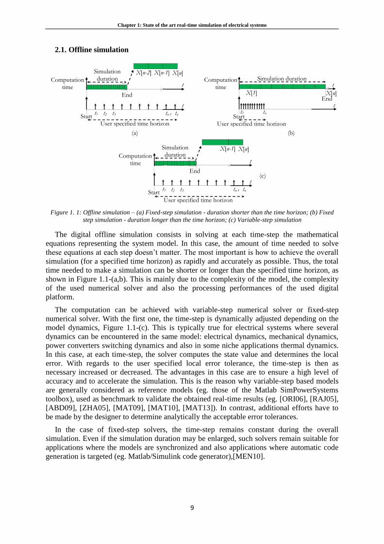
2.1. Offline simulation
Figure 1. 1: Offline simulation – (a) Fixed-step simulation - duration shorter than the time horizon; (b) Fixed
step simulation - duration longer than the time horizon; (c) Variable-step simulation
The digital offline simulation consists in solving at each time-step the mathematical
equations representing the system model. In this case, the amount of time needed to solve
these equations at each step doesn’t matter. The most important is how to achieve the overall
simulation (for a specified time horizon) as rapidly and accurately as possible. Thus, the total
time needed to make a simulation can be shorter or longer than the specified time horizon, as
shown in Figure 1.1-(a,b). This is mainly due to the complexity of the model, the complexity
of the used numerical solver and also the processing performances of the used digital
platform.
The computation can be achieved with variable-step numerical solver or fixed-step
numerical solver. With the first one, the time-step is dynamically adjusted depending on the
model dynamics, Figure 1.1-(c). This is typically true for electrical systems where several
dynamics can be encountered in the same model: electrical dynamics, mechanical dynamics,
power converters switching dynamics and also in some niche applications thermal dynamics.
In this case, at each time-step, the solver computes the state value and determines the local
error. With regards to the user specified local error tolerance, the time-step is then as
necessary increased or decreased. The advantages in this case are to ensure a high level of
accuracy and to accelerate the simulation. This is the reason why variable-step based models
are generally considered as reference models (eg. those of the Matlab SimPowerSystems
toolbox), used as benchmark to validate the obtained real-time results (eg. [ORI06], [RAJ05],
[ABD09], [ZHA05], [MAT09], [MAT10], [MAT13]). In contrast, additional efforts have to
be made by the designer to determine analytically the acceptable error tolerances.
In the case of fixed-step solvers, the time-step remains constant during the overall
simulation. Even if the simulation duration may be enlarged, such solvers remain suitable for
applications where the models are synchronized and also applications where automatic code
generation is targeted (eg. Matlab/Simulink code generator),[MEN10].
Start
End
Simulation duration
User specified time horizon
t1 t2 t3 tn-1 tn
X[n-2] X[n-1] X[n]
t
t
(a)
Computation time
Start
End
Simulation duration
tn
X[n]
t
t
t1
X[1]
(b)
Computation time
Start
End
Simulation duration
t1 t2 t3 tn-1 tn
X[n-1] X[n]
t
t
(c)
Computation time
User specified time horizon
User specified time horizon
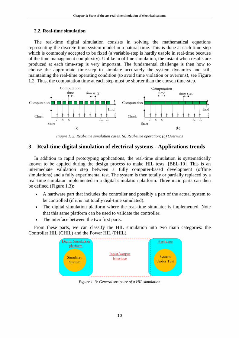
Chapter 1: State of the art real-time simulation of electrical systems
10
2.2. Real-time simulation
The real-time digital simulation consists in solving the mathematical equations
representing the discrete-time system model in a natural time. This is done at each time-step
which is commonly accepted to be fixed (a variable-step is hardly usable in real-time because
of the time management complexity). Unlike in offline simulation, the instant when results are
produced at each time-step is very important. The fundamental challenge is then how to
choose the appropriate time-step to simulate accurately the system dynamics and still
maintaining the real-time operating condition (to avoid time violation or overruns), see Figure
1.2. Thus, the computation time at each step must be shorter than the chosen time-step.
Figure 1. 2: Real-time simulation cases. (a) Real-time operation; (b) Overruns
3. Real-time digital simulation of electrical systems - Applications trends
In addition to rapid prototyping applications, the real-time simulation is systematically
known to be applied during the design process to make HIL tests, [BEL-10]. This is an
intermediate validation step between a fully computer-based development (offline
simulations) and a fully experimental test. The system is then totally or partially replaced by a
real-time simulator implemented in a digital simulation platform. Three main parts can then
be defined (Figure 1.3):
A hardware part that includes the controller and possibly a part of the actual system to
be controlled (if it is not totally real-time simulated).
The digital simulation platform where the real-time simulator is implemented. Note
that this same platform can be used to validate the controller.
The interface between the two first parts.
From these parts, we can classify the HIL simulation into two main categories: the
Controller HIL (CHIL) and the Power HIL (PHIL).
Figure 1. 3: General structure of a HIL simulation
Digital Simulation platform
Simulated System
Hardware
System Under Test
Input/output Interface
time-step
Computation time
Clock t
t1 t2 t3 tn-1 tn
t
Start
End
Computation
(b)
time-step
Computation time
Clock t
t1 t2 t3 tn-1 tn
t
Start
End
Computation
(a)
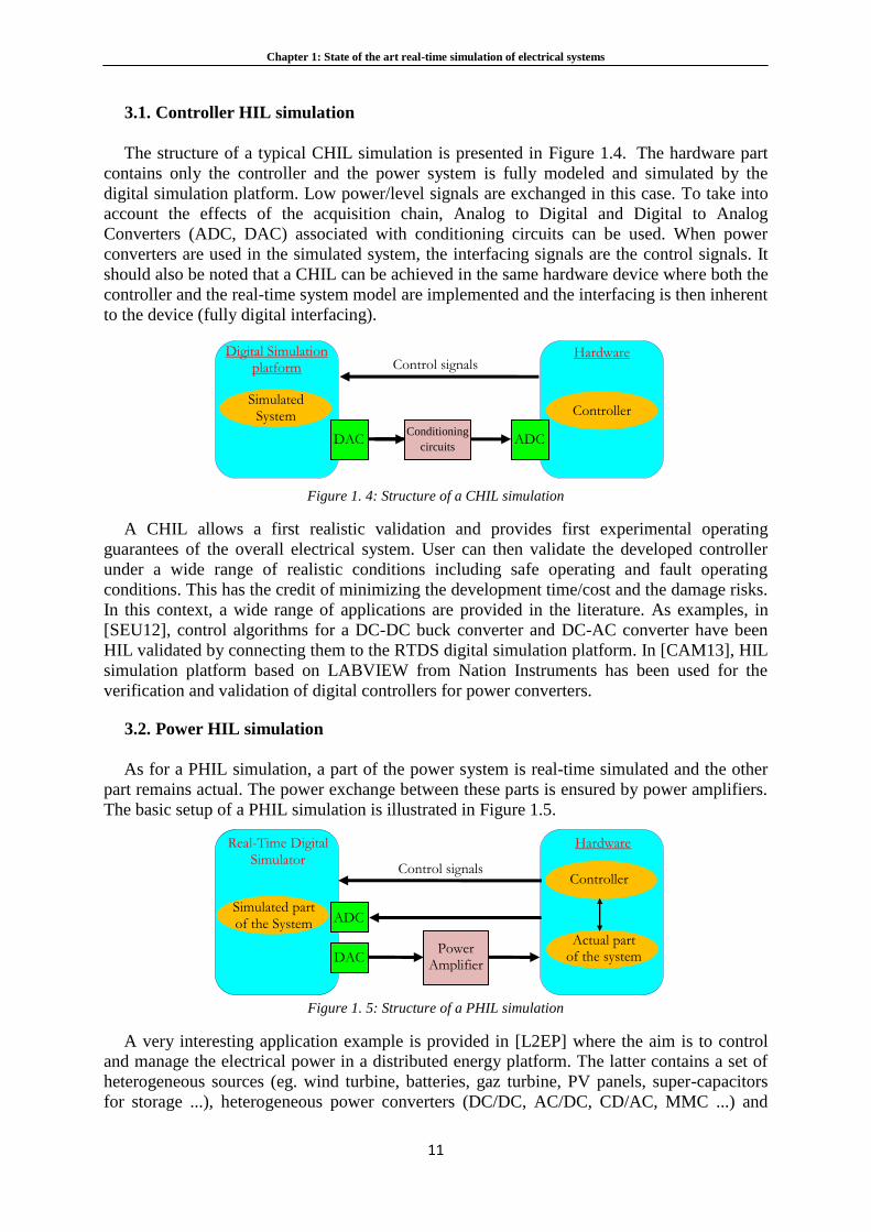
Chapter 1: State of the art real-time simulation of electrical systems
11
3.1. Controller HIL simulation
The structure of a typical CHIL simulation is presented in Figure 1.4. The hardware part
contains only the controller and the power system is fully modeled and simulated by the
digital simulation platform. Low power/level signals are exchanged in this case. To take into
account the effects of the acquisition chain, Analog to Digital and Digital to Analog
Converters (ADC, DAC) associated with conditioning circuits can be used. When power
converters are used in the simulated system, the interfacing signals are the control signals. It
should also be noted that a CHIL can be achieved in the same hardware device where both the
controller and the real-time system model are implemented and the interfacing is then inherent
to the device (fully digital interfacing).
Figure 1. 4: Structure of a CHIL simulation
A CHIL allows a first realistic validation and provides first experimental operating
guarantees of the overall electrical system. User can then validate the developed controller
under a wide range of realistic conditions including safe operating and fault operating
conditions. This has the credit of minimizing the development time/cost and the damage risks.
In this context, a wide range of applications are provided in the literature. As examples, in
[SEU12], control algorithms for a DC-DC buck converter and DC-AC converter have been
HIL validated by connecting them to the RTDS digital simulation platform. In [CAM13], HIL
simulation platform based on LABVIEW from Nation Instruments has been used for the
verification and validation of digital controllers for power converters.
3.2. Power HIL simulation
As for a PHIL simulation, a part of the power system is real-time simulated and the other
part remains actual. The power exchange between these parts is ensured by power amplifiers.
The basic setup of a PHIL simulation is illustrated in Figure 1.5.
Figure 1. 5: Structure of a PHIL simulation
A very interesting application example is provided in [L2EP] where the aim is to control
and manage the electrical power in a distributed energy platform. The latter contains a set of
heterogeneous sources (eg. wind turbine, batteries, gaz turbine, PV panels, super-capacitors
for storage ...), heterogeneous power converters (DC/DC, AC/DC, CD/AC, MMC ...) and
Real-Time Digital Simulator
ADC
DAC Power
Amplifier
Hardware
Simulated part of the System
Actual part of the system
Controller Control signals
Digital Simulation platform
ADC DAC
Simulated System
Hardware
Controller
Control signals
Conditioning
circuits
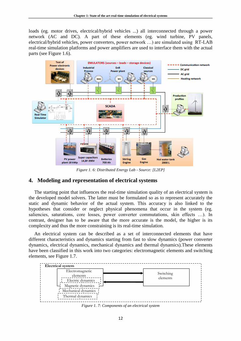
Chapter 1: State of the art real-time simulation of electrical systems
12
loads (eg. motor drives, electrical/hybrid vehicles ...) all interconnected through a power
network (AC and DC). A part of these elements (eg. wind turbine, PV panels,
electrical/hybrid vehicles, power converters, power network …) are simulated using RT-LAB
real-time simulation platforms and power amplifiers are used to interface them with the actual
parts (see Figure 1.6).
Figure 1. 6: Distributed Energy Lab - Source: [L2EP]
4. Modeling and representation of electrical systems
The starting point that influences the real-time simulation quality of an electrical system is
the developed model solvers. The latter must be formulated so as to represent accurately the
static and dynamic behavior of the actual system. This accuracy is also linked to the
hypotheses that consider or neglect physical phenomena that occur in the system (eg.
saliencies, saturations, core losses, power converter commutations, skin effects …). In
contrast, designer has to be aware that the more accurate is the model, the higher is its
complexity and thus the more constraining is its real-time simulation.
An electrical system can be described as a set of interconnected elements that have
different characteristics and dynamics starting from fast to slow dynamics (power converter
dynamics, electrical dynamics, mechanical dynamics and thermal dynamics).These elements
have been classified in this work into two categories: electromagnetic elements and switching
elements, see Figure 1.7.
Figure 1. 7: Components of an electrical system
Electrical system
Electromagnetic elements
Switching elements
Electric dynamics
Mechanical dynamics
Thermal dynamics
Magnetic dynamics
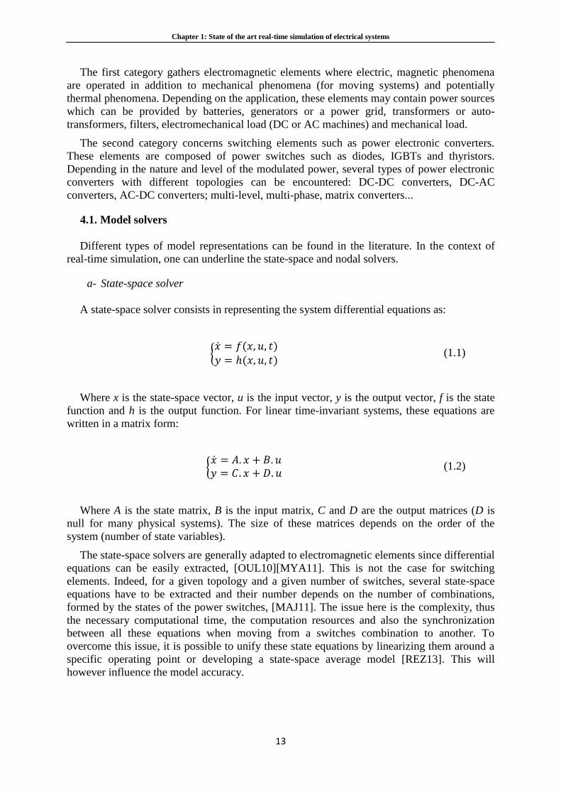
Chapter 1: State of the art real-time simulation of electrical systems
13
The first category gathers electromagnetic elements where electric, magnetic phenomena
are operated in addition to mechanical phenomena (for moving systems) and potentially
thermal phenomena. Depending on the application, these elements may contain power sources
which can be provided by batteries, generators or a power grid, transformers or auto-
transformers, filters, electromechanical load (DC or AC machines) and mechanical load.
The second category concerns switching elements such as power electronic converters.
These elements are composed of power switches such as diodes, IGBTs and thyristors.
Depending in the nature and level of the modulated power, several types of power electronic
converters with different topologies can be encountered: DC-DC converters, DC-AC
converters, AC-DC converters; multi-level, multi-phase, matrix converters...
4.1. Model solvers
Different types of model representations can be found in the literature. In the context of
real-time simulation, one can underline the state-space and nodal solvers.
a- State-space solver
A state-space solver consists in representing the system differential equations as:
= 𝑓(𝑥, 𝑢, 𝑡)𝑦 = ℎ(𝑥, 𝑢, 𝑡)
(1.1)
Where x is the state-space vector, u is the input vector, y is the output vector, f is the state
function and h is the output function. For linear time-invariant systems, these equations are
written in a matrix form:
= 𝐴. 𝑥 + 𝐵. 𝑢𝑦 = 𝐶. 𝑥 + 𝐷. 𝑢
(1.2)
Where A is the state matrix, B is the input matrix, C and D are the output matrices (D is
null for many physical systems). The size of these matrices depends on the order of the
system (number of state variables).
The state-space solvers are generally adapted to electromagnetic elements since differential
equations can be easily extracted, [OUL10][MYA11]. This is not the case for switching
elements. Indeed, for a given topology and a given number of switches, several state-space
equations have to be extracted and their number depends on the number of combinations,
formed by the states of the power switches, [MAJ11]. The issue here is the complexity, thus
the necessary computational time, the computation resources and also the synchronization
between all these equations when moving from a switches combination to another. To
overcome this issue, it is possible to unify these state equations by linearizing them around a
specific operating point or developing a state-space average model [REZ13]. This will
however influence the model accuracy.
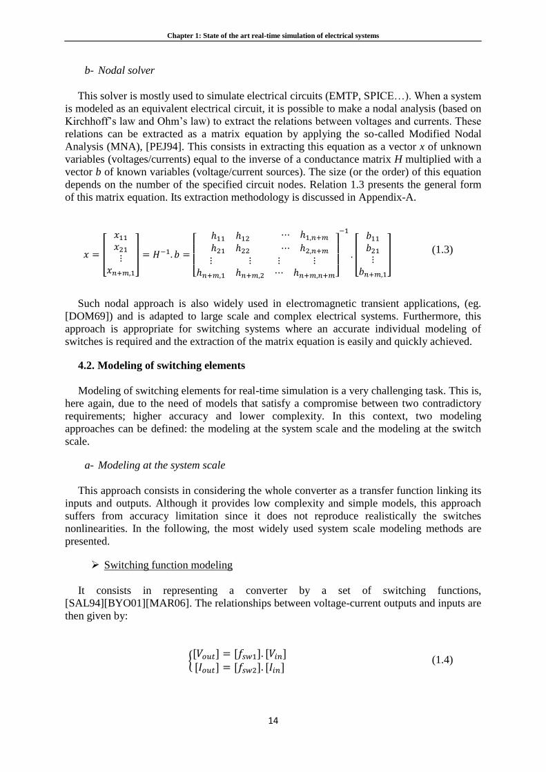
Chapter 1: State of the art real-time simulation of electrical systems
14
b- Nodal solver
This solver is mostly used to simulate electrical circuits (EMTP, SPICE…). When a system
is modeled as an equivalent electrical circuit, it is possible to make a nodal analysis (based on
Kirchhoff’s law and Ohm’s law) to extract the relations between voltages and currents. These
relations can be extracted as a matrix equation by applying the so-called Modified Nodal
Analysis (MNA), [PEJ94]. This consists in extracting this equation as a vector x of unknown
variables (voltages/currents) equal to the inverse of a conductance matrix H multiplied with a
vector b of known variables (voltage/current sources). The size (or the order) of this equation
depends on the number of the specified circuit nodes. Relation 1.3 presents the general form
of this matrix equation. Its extraction methodology is discussed in Appendix-A.
𝑥 = [
𝑥11𝑥21⋮
𝑥𝑛+𝑚,1
] = 𝐻−1. 𝑏 =
[
ℎ11 ℎ12ℎ21 ℎ22
⋯ ℎ1,𝑛+𝑚⋯ ℎ2,𝑛+𝑚
⋮ ⋮ℎ𝑛+𝑚,1 ℎ𝑛+𝑚,2
⋮ ⋮⋯ ℎ𝑛+𝑚,𝑛+𝑚]
−1
. [
𝑏11𝑏21⋮
𝑏𝑛+𝑚,1
] (1.3)
Such nodal approach is also widely used in electromagnetic transient applications, (eg.
[DOM69]) and is adapted to large scale and complex electrical systems. Furthermore, this
approach is appropriate for switching systems where an accurate individual modeling of
switches is required and the extraction of the matrix equation is easily and quickly achieved.
4.2. Modeling of switching elements
Modeling of switching elements for real-time simulation is a very challenging task. This is,
here again, due to the need of models that satisfy a compromise between two contradictory
requirements; higher accuracy and lower complexity. In this context, two modeling
approaches can be defined: the modeling at the system scale and the modeling at the switch
scale.
a- Modeling at the system scale
This approach consists in considering the whole converter as a transfer function linking its
inputs and outputs. Although it provides low complexity and simple models, this approach
suffers from accuracy limitation since it does not reproduce realistically the switches
nonlinearities. In the following, the most widely used system scale modeling methods are
presented.
Switching function modeling
It consists in representing a converter by a set of switching functions,
[SAL94][BYO01][MAR06]. The relationships between voltage-current outputs and inputs are
then given by:
[𝑉𝑜𝑢𝑡] = [𝑓𝑠𝑤1]. [𝑉𝑖𝑛][𝐼𝑜𝑢𝑡] = [𝑓𝑠𝑤2]. [𝐼𝑖𝑛]
(1.4)
Chapter 1: State of the art real-time simulation of electrical systems
15
Where, Vout and Vin are the vectors of output voltages and input voltages, respectively. Iout
and Iin are the vectors of output currents and input currents, respectively. fsw1 and fsw2 are the
switching functions which depend on the control signals Ci.
As an example, the modeling of a 3-phase inverter (Figure 1.8) gives the following
equations:
Figure 1. 8: Circuit diagram of a 3-phase inverter
[𝑉𝑜𝑢𝑡] = [
𝑣𝐿𝑎𝑣𝐿𝑏𝑣𝐿𝑐
] =1
3[
2. 𝐶1 − 𝐶2 − 𝐶3−𝐶1 + 2. 𝐶2 − 𝐶3−𝐶1 − 𝐶2 + 2. 𝐶3
] . [𝑉𝑑𝑐] = [𝑓𝑠𝑤1]. [𝑉𝑖𝑛]
[𝐼𝑜𝑢𝑡] = [𝐼𝑑𝑐] = [𝐶1 𝐶2 𝐶3]. [𝑖𝐿𝑎𝑖𝐿𝑏𝑖𝐿𝑐
] = [𝑓𝑠𝑤2]. [𝐼𝑖𝑛]
(1.5)
This modeling method is highly dependent on the converter topology. It is then not suitable
when complex topologies (eg. Multi-level converter, Matrix converters) are considered. It is
also worth noticing that this method is not able to represent anti-parallel natural switching
diodes and therefore, for the proposed example, the rectifier mode is not ensured [SYB06]. To
cope with this problem, an efficient solution consists in describing the behavior of the
converter using a state machine. This solution has been applied in [RAK11] to design a
switching function model of three-level neutral-clamped that support rectifier mode.
Averaged modeling
An averaged modeling approach considers only the average value of the system variables
in addition to the control signals duty cycle [JIN97], [KIF11]. Generally, the averaging is
made over one switching period and the oscillations (due to commutations) are not considered
leading to a relatively simple model.
Staying with the same example as before, to obtain the average model of a 3-phase
inverter, the moving average equation defined by relation 1.6 is applied to the equations 1.5.
⟨𝑣𝑎𝑟𝑖𝑎𝑏𝑙𝑒⟩ =1
𝑇∫ 𝑣𝑎𝑟𝑖𝑎𝑏𝑙𝑒(𝑡). 𝑑𝑡
(𝑘+1)𝑇
𝑘𝑇
(1.6)
The obtained equations (over one switching period) are then:
C2 C3
vLa
vLb
vLc
C2 C3
C1
C1
Idc
iLa
iLb
iLc
Vdc
Chapter 1: State of the art real-time simulation of electrical systems
16
[
⟨𝑣𝐿𝑎⟩
⟨𝑣𝐿𝑏⟩
⟨𝑣𝐿𝑐⟩] =
1
3[
2⟨𝐶1. 𝑉𝑑𝑐⟩ − ⟨𝐶2. 𝑉𝑑𝑐⟩ − ⟨𝐶3. 𝑉𝑑𝑐⟩
−⟨𝐶1. 𝑉𝑑𝑐⟩ + 2⟨𝐶2. 𝑉𝑑𝑐⟩ − ⟨𝐶3. 𝑉𝑑𝑐⟩
−⟨𝐶1. 𝑉𝑑𝑐⟩ − ⟨𝐶2. 𝑉𝑑𝑐⟩ + 2⟨𝐶3. 𝑉𝑑𝑐⟩]
[⟨𝐼𝑑𝑐⟩] = [⟨𝐶1. 𝑖𝐿𝑎⟩ + ⟨𝐶2. 𝑖𝐿𝑏⟩ + ⟨𝐶3. 𝑖𝐿𝑐⟩]
(1.7)
Note that the following simplifications can be applied when the averaging is made over
one switching period.
⟨𝐶𝑖. 𝑉𝑑𝑐⟩ = ⟨𝐶𝑖⟩. ⟨𝑉𝑑𝑐⟩
⟨𝐶𝑖. 𝑖𝑖⟩ = ⟨𝐶𝑖⟩. ⟨𝑖𝑖⟩ (1.8)
The main drawback of such approach is that the commutation events are not covered
during a switching period which limits the bandwidth and the accuracy of the model. An
alternative to overtake this issue consists in averaging the model over one simulation time-
step instead one switching period [LIA05]. This is possible of course since the simulation
time-step is typically much lower than the switching period.
b- Modeling at the switch scale
This approach consists in modeling each switch individually. Unlike system scale
modeling, it allows representing the turn-on and turn-off nonlinear characteristics, the
switching power losses [MYA11], and even the thermal characteristics [KRU99] of the
switches. In the following, the most widely used switch scale modeling methods are
presented.
Physical modeling
It consists in modeling each switch by its physical model. This latter is generally based on
semiconductor physics describing the charge carrier distribution in the device. As an example,
the most popular physical models used for IGBTs modeling are the Hefner [HEF88] and
Kraus [KRA93] which have been implemented in offline simulators such as SABER and
SPICE. This method is well-known for its notable accuracy. However, its use remains limited
in real-time simulation because it leads to complex models which are difficult to be
implemented in real-time.
Behavioral modeling
It consists in representing each switch by its voltage and current characteristics obtained
either from fitting curves [BLA96] or experimentations [MYA11]. The converter model is
then represented by a state machine which interacts at high rate with memories where these
characteristics are stored. As an example, in [MYA11], a device-level behavioral model of an
IGBT-based multilevel voltage source converter has been implemented. In this example, the
voltage and current characteristics of the IGBT module (CM50DU-24F from Powerex) are
obtained from an experimental setup (Figure 1.9, extracted from [MYA11]).
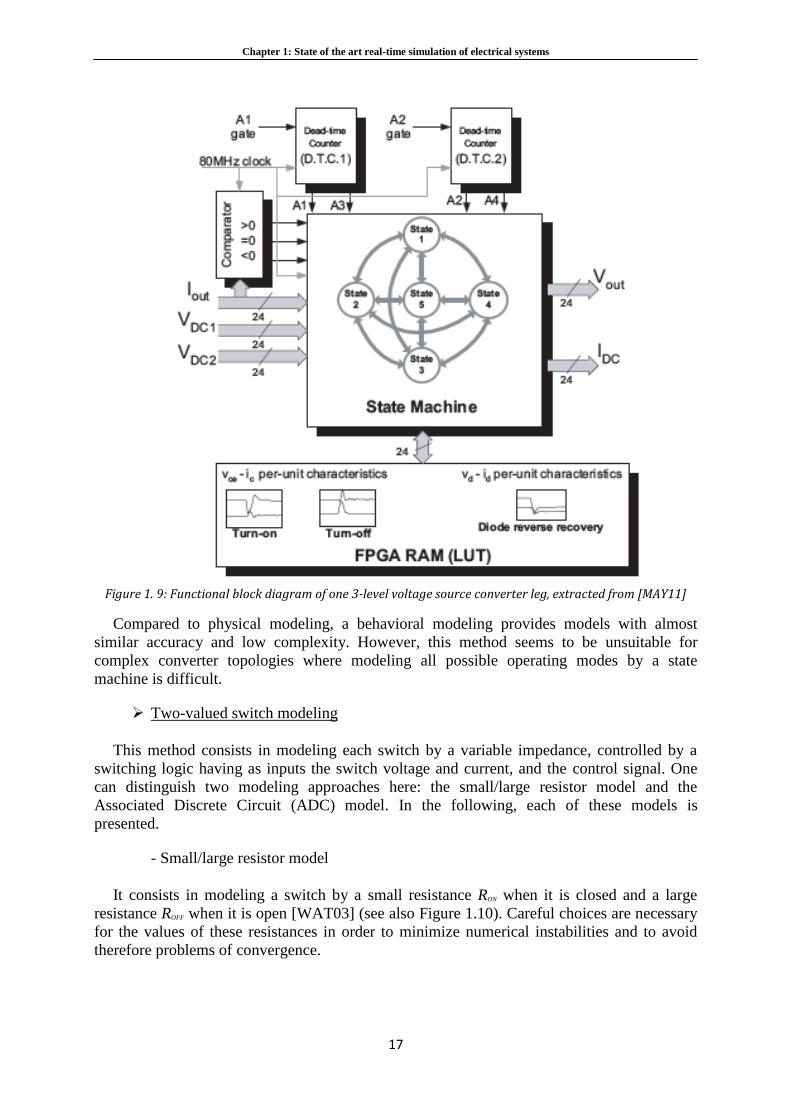
Chapter 1: State of the art real-time simulation of electrical systems
17
Figure 1. 9: Functional block diagram of one 3-level voltage source converter leg, extracted from [MAY11]
Compared to physical modeling, a behavioral modeling provides models with almost
similar accuracy and low complexity. However, this method seems to be unsuitable for
complex converter topologies where modeling all possible operating modes by a state
machine is difficult.
Two-valued switch modeling
This method consists in modeling each switch by a variable impedance, controlled by a
switching logic having as inputs the switch voltage and current, and the control signal. One
can distinguish two modeling approaches here: the small/large resistor model and the
Associated Discrete Circuit (ADC) model. In the following, each of these models is
presented.
- Small/large resistor model
It consists in modeling a switch by a small resistance RON when it is closed and a large
resistance ROFF when it is open [WAT03] (see also Figure 1.10). Careful choices are necessary
for the values of these resistances in order to minimize numerical instabilities and to avoid
therefore problems of convergence.
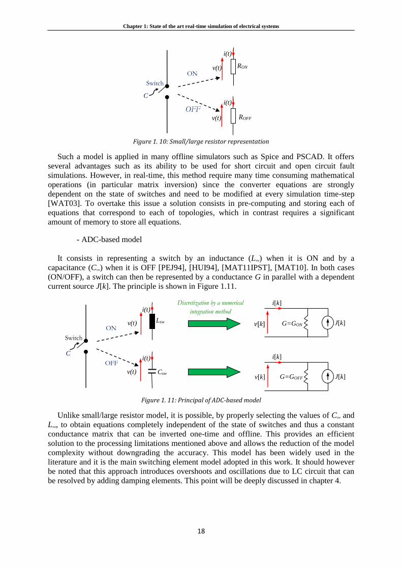
Chapter 1: State of the art real-time simulation of electrical systems
18
Figure 1. 10: Small/large resistor representation
Such a model is applied in many offline simulators such as Spice and PSCAD. It offers
several advantages such as its ability to be used for short circuit and open circuit fault
simulations. However, in real-time, this method require many time consuming mathematical
operations (in particular matrix inversion) since the converter equations are strongly
dependent on the state of switches and need to be modified at every simulation time-step
[WAT03]. To overtake this issue a solution consists in pre-computing and storing each of
equations that correspond to each of topologies, which in contrast requires a significant
amount of memory to store all equations.
- ADC-based model
It consists in representing a switch by an inductance (Lsw) when it is ON and by a
capacitance (Csw) when it is OFF [PEJ94], [HUI94], [MAT11IPST], [MAT10]. In both cases
(ON/OFF), a switch can then be represented by a conductance G in parallel with a dependent
current source J[k]. The principle is shown in Figure 1.11.
Figure 1. 11: Principal of ADC-based model
Unlike small/large resistor model, it is possible, by properly selecting the values of Csw and
Lsw, to obtain equations completely independent of the state of switches and thus a constant
conductance matrix that can be inverted one-time and offline. This provides an efficient
solution to the processing limitations mentioned above and allows the reduction of the model
complexity without downgrading the accuracy. This model has been widely used in the
literature and it is the main switching element model adopted in this work. It should however
be noted that this approach introduces overshoots and oscillations due to LC circuit that can
be resolved by adding damping elements. This point will be deeply discussed in chapter 4.
i[k]
v[k] J[k] Lsw G=GON
Discretization by a numerical
integration method
ON
OFF
i[k]
v[k] G=GOFF J[k] Csw
i(t)
i(t)
Switch
C
v(t)
v(t)
RON ON
OFF
ROFF
i(t)
i(t)
Switch
C
v(t)
v(t)
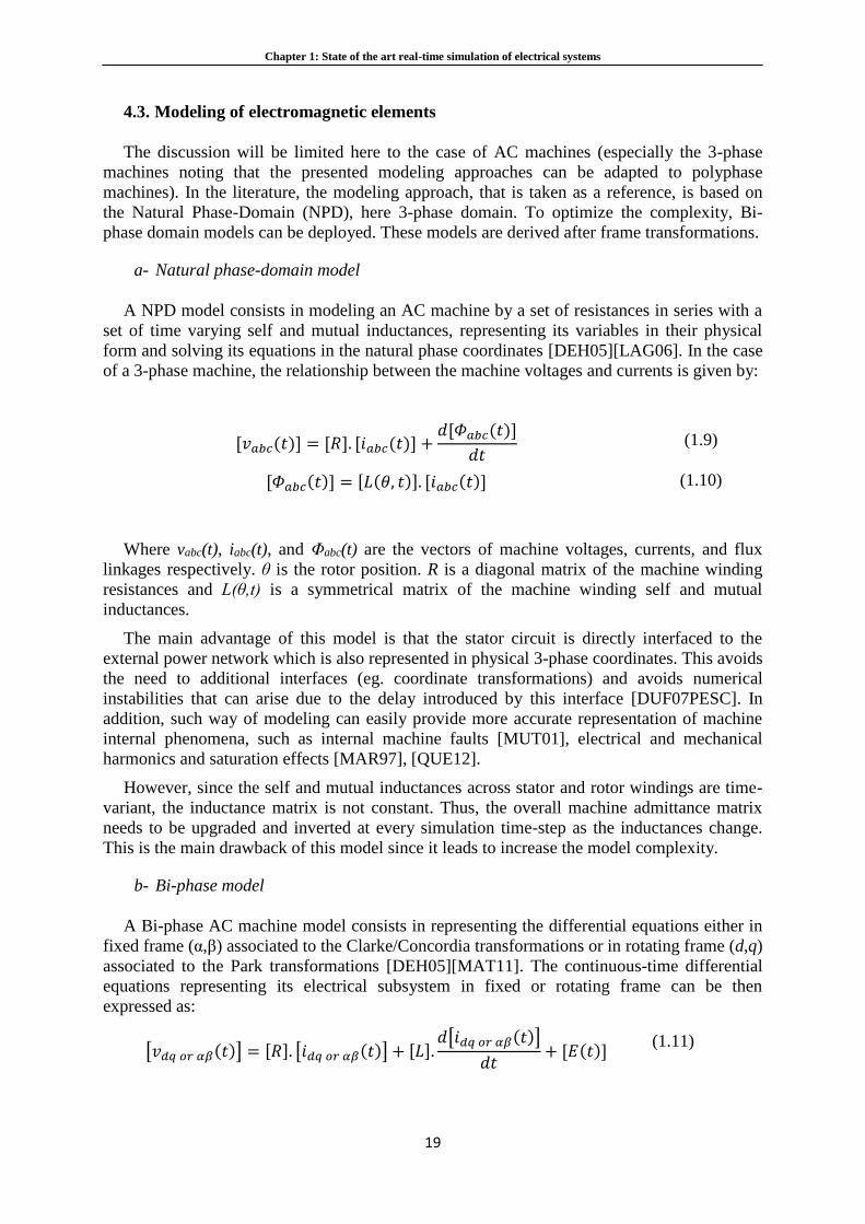
Chapter 1: State of the art real-time simulation of electrical systems
19
4.3. Modeling of electromagnetic elements
The discussion will be limited here to the case of AC machines (especially the 3-phase
machines noting that the presented modeling approaches can be adapted to polyphase
machines). In the literature, the modeling approach, that is taken as a reference, is based on
the Natural Phase-Domain (NPD), here 3-phase domain. To optimize the complexity, Bi-
phase domain models can be deployed. These models are derived after frame transformations.
a- Natural phase-domain model
A NPD model consists in modeling an AC machine by a set of resistances in series with a
set of time varying self and mutual inductances, representing its variables in their physical
form and solving its equations in the natural phase coordinates [DEH05][LAG06]. In the case
of a 3-phase machine, the relationship between the machine voltages and currents is given by:
[𝑣𝑎𝑏𝑐(𝑡)] = [𝑅]. [𝑖𝑎𝑏𝑐(𝑡)] +𝑑[𝛷𝑎𝑏𝑐(𝑡)]
𝑑𝑡 (1.9)
[𝛷𝑎𝑏𝑐(𝑡)] = [𝐿(𝜃, 𝑡)]. [𝑖𝑎𝑏𝑐(𝑡)] (1.10)
Where vabc(t), iabc(t), and Φabc(t) are the vectors of machine voltages, currents, and flux
linkages respectively. θ is the rotor position. R is a diagonal matrix of the machine winding
resistances and L(θ,t) is a symmetrical matrix of the machine winding self and mutual
inductances.
The main advantage of this model is that the stator circuit is directly interfaced to the
external power network which is also represented in physical 3-phase coordinates. This avoids
the need to additional interfaces (eg. coordinate transformations) and avoids numerical
instabilities that can arise due to the delay introduced by this interface [DUF07PESC]. In
addition, such way of modeling can easily provide more accurate representation of machine
internal phenomena, such as internal machine faults [MUT01], electrical and mechanical
harmonics and saturation effects [MAR97], [QUE12].
However, since the self and mutual inductances across stator and rotor windings are time-
variant, the inductance matrix is not constant. Thus, the overall machine admittance matrix
needs to be upgraded and inverted at every simulation time-step as the inductances change.
This is the main drawback of this model since it leads to increase the model complexity.
b- Bi-phase model
A Bi-phase AC machine model consists in representing the differential equations either in
fixed frame (α,β) associated to the Clarke/Concordia transformations or in rotating frame (d,q)
associated to the Park transformations [DEH05][MAT11]. The continuous-time differential
equations representing its electrical subsystem in fixed or rotating frame can be then
expressed as:
[𝑣𝑑𝑞 𝑜𝑟 𝛼𝛽(𝑡)] = [𝑅]. [𝑖𝑑𝑞 𝑜𝑟 𝛼𝛽(𝑡)] + [𝐿].𝑑[𝑖𝑑𝑞 𝑜𝑟 𝛼𝛽(𝑡)]
𝑑𝑡+ [𝐸(𝑡)]
(1.11)
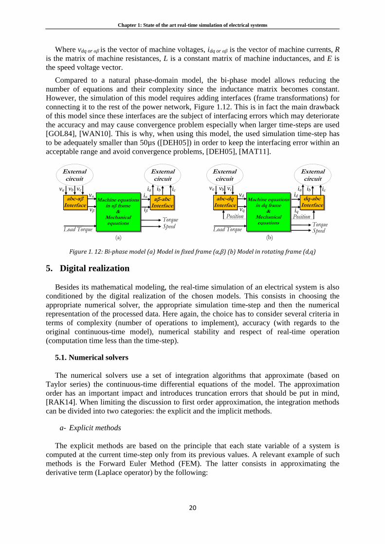
Chapter 1: State of the art real-time simulation of electrical systems
20
Where vdq or αβ is the vector of machine voltages, idq or αβ is the vector of machine currents, R
is the matrix of machine resistances, L is a constant matrix of machine inductances, and E is
the speed voltage vector.
Compared to a natural phase-domain model, the bi-phase model allows reducing the
number of equations and their complexity since the inductance matrix becomes constant.
However, the simulation of this model requires adding interfaces (frame transformations) for
connecting it to the rest of the power network, Figure 1.12. This is in fact the main drawback
of this model since these interfaces are the subject of interfacing errors which may deteriorate
the accuracy and may cause convergence problem especially when larger time-steps are used
[GOL84], [WAN10]. This is why, when using this model, the used simulation time-step has
to be adequately smaller than 50µs ([DEH05]) in order to keep the interfacing error within an
acceptable range and avoid convergence problems, [DEH05], [MAT11].
Figure 1. 12: Bi-phase model (a) Model in fixed frame (α,β) (b) Model in rotating frame (d,q)
5. Digital realization
Besides its mathematical modeling, the real-time simulation of an electrical system is also
conditioned by the digital realization of the chosen models. This consists in choosing the
appropriate numerical solver, the appropriate simulation time-step and then the numerical
representation of the processed data. Here again, the choice has to consider several criteria in
terms of complexity (number of operations to implement), accuracy (with regards to the
original continuous-time model), numerical stability and respect of real-time operation
(computation time less than the time-step).
5.1. Numerical solvers
The numerical solvers use a set of integration algorithms that approximate (based on
Taylor series) the continuous-time differential equations of the model. The approximation
order has an important impact and introduces truncation errors that should be put in mind,
[RAK14]. When limiting the discussion to first order approximation, the integration methods
can be divided into two categories: the explicit and the implicit methods.
a- Explicit methods
The explicit methods are based on the principle that each state variable of a system is
computed at the current time-step only from its previous values. A relevant example of such
methods is the Forward Euler Method (FEM). The latter consists in approximating the
derivative term (Laplace operator) by the following:
abc-αβ Interface
ia ib ic
External circuit
Load Torque
Torque Speed
Machine equations in αβ frame
& Mechanical equations
va vb vc
αβ-abc Interface
External circuit
abc-dq Interface
ia ib ic
External circuit
Load Torque Torque Speed
Machine equations in dq frame
& Mechanical equations
va vb vc
dq-abc Interface
External circuit
Position Position
(a) (b)
iα
iβ
vα
vβ
vd
vq
id
iq
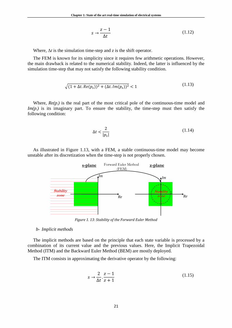
Chapter 1: State of the art real-time simulation of electrical systems
21
𝑠 →𝑧 − 1
∆𝑡 (1.12)
Where, ∆t is the simulation time-step and z is the shift operator.
The FEM is known for its simplicity since it requires few arithmetic operations. However,
the main drawback is related to the numerical stability. Indeed, the latter is influenced by the
simulation time-step that may not satisfy the following stability condition.
√(1 + ∆𝑡. 𝑅𝑒(𝑝𝑠))2 + (∆𝑡. 𝐼𝑚(𝑝𝑠))
2 < 1 (1.13)
Where, Re(ps) is the real part of the most critical pole of the continuous-time model and
Im(ps) is its imaginary part. To ensure the stability, the time-step must then satisfy the
following condition:
∆𝑡 <2
|𝑝𝑠| (1.14)
As illustrated in Figure 1.13, with a FEM, a stable continuous-time model may become
unstable after its discretization when the time-step is not properly chosen.
Figure 1. 13: Stability of the Forward Euler Method
b- Implicit methods
The implicit methods are based on the principle that each state variable is processed by a
combination of its current value and the previous values. Here, the Implicit Trapezoidal
Method (ITM) and the Backward Euler Method (BEM) are mostly deployed.
The ITM consists in approximating the derivative operator by the following:
𝑠 →2
∆𝑡.𝑧 − 1
𝑧 + 1
(1.15)
Im
Re
1
Im
Re
s-plane z-plane
Stability zone
Stability zone
Forward Euler Method (FEM)
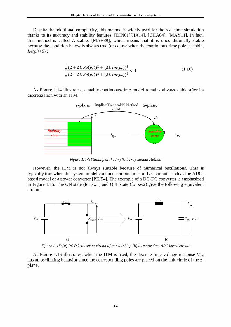
Chapter 1: State of the art real-time simulation of electrical systems
22
Despite the additional complexity, this method is widely used for the real-time simulation
thanks to its accuracy and stability features, [DIN01][JIA14], [CHA04], [MAY11]. In fact,
this method is called A-stable, [MAR89], which means that it is unconditionally stable
because the condition below is always true (of course when the continuous-time pole is stable,
Re(ps)<0) :
√(2 + ∆𝑡. 𝑅𝑒(𝑝𝑠))2 + (∆𝑡. 𝐼𝑚(𝑝𝑠))
2
√(2 − ∆𝑡. 𝑅𝑒(𝑝𝑠))2 + (∆𝑡. 𝐼𝑚(𝑝𝑠))
2< 1 (1.16)
As Figure 1.14 illustrates, a stable continuous-time model remains always stable after its
discretization with an ITM.
Figure 1. 14: Stability of the Implicit Trapezoidal Method
However, the ITM is not always suitable because of numerical oscillations. This is
typically true when the system model contains combinations of L-C circuits such as the ADC-
based model of a power converter [PEJ94]. The example of a DC-DC converter is emphasized
in Figure 1.15. The ON state (for sw1) and OFF state (for sw2) give the following equivalent
circuit:
Figure 1. 15: (a) DC-DC converter circuit after switching (b) its equivalent ADC-based circuit
As Figure 1.16 illustrates, when the ITM is used, the discrete-time voltage response Vout
has an oscillating behavior since the corresponding poles are placed on the unit circle of the z-
plane.
sw1
sw2
Lsw
Csw Vdc
iL iL
Vdc Vout Vout
(a) (b)
Im
Re 1
Im
Re
s-plane z-plane
Stability zone
Stability zone
Implicit Trapezoidal Method (ITM)
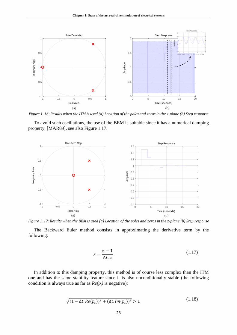
Chapter 1: State of the art real-time simulation of electrical systems
23
Figure 1. 16: Results when the ITM is used (a) Location of the poles and zeros in the z-plane (b) Step response
To avoid such oscillations, the use of the BEM is suitable since it has a numerical damping
property, [MAR89], see also Figure 1.17.
Figure 1. 17: Results when the BEM is used (a) Location of the poles and zeros in the z-plane (b) Step response
The Backward Euler method consists in approximating the derivative term by the
following:
𝑠 =𝑧 − 1
∆𝑡. 𝑧
(1.17)
In addition to this damping property, this method is of course less complex than the ITM
one and has the same stability feature since it is also unconditionally stable (the following
condition is always true as far as Re(ps) is negative):
√(1 − ∆𝑡. 𝑅𝑒(𝑝𝑠))2 + (∆𝑡. 𝐼𝑚(𝑝𝑠))
2 > 1 (1.18)
-1 -0.5 0 0.5 1-1
-0.5
0
0.5
1
Pole-Zero Map
Real Axis
Imagin
ary
Axis
0 5 10 15 200.4
0.5
0.6
0.7
0.8
0.9
1
1.1
1.2
1.3Step Response
Time (seconds)
Am
plit
ude
(a) (b)
-1 -0.5 0 0.5 1-1
-0.5
0
0.5
1
Pole-Zero Map
Real Axis
Imagin
ary
Axis
0 5 10 15 200
0.5
1
1.5
2
Step Response
Time (seconds)
Am
plit
ude
11.49 11.5 11.51 11.52 11.53 11.54
-2
-1
0
1
2
3
Step Response
Time (seconds)
Am
plit
ude
(a) (b)
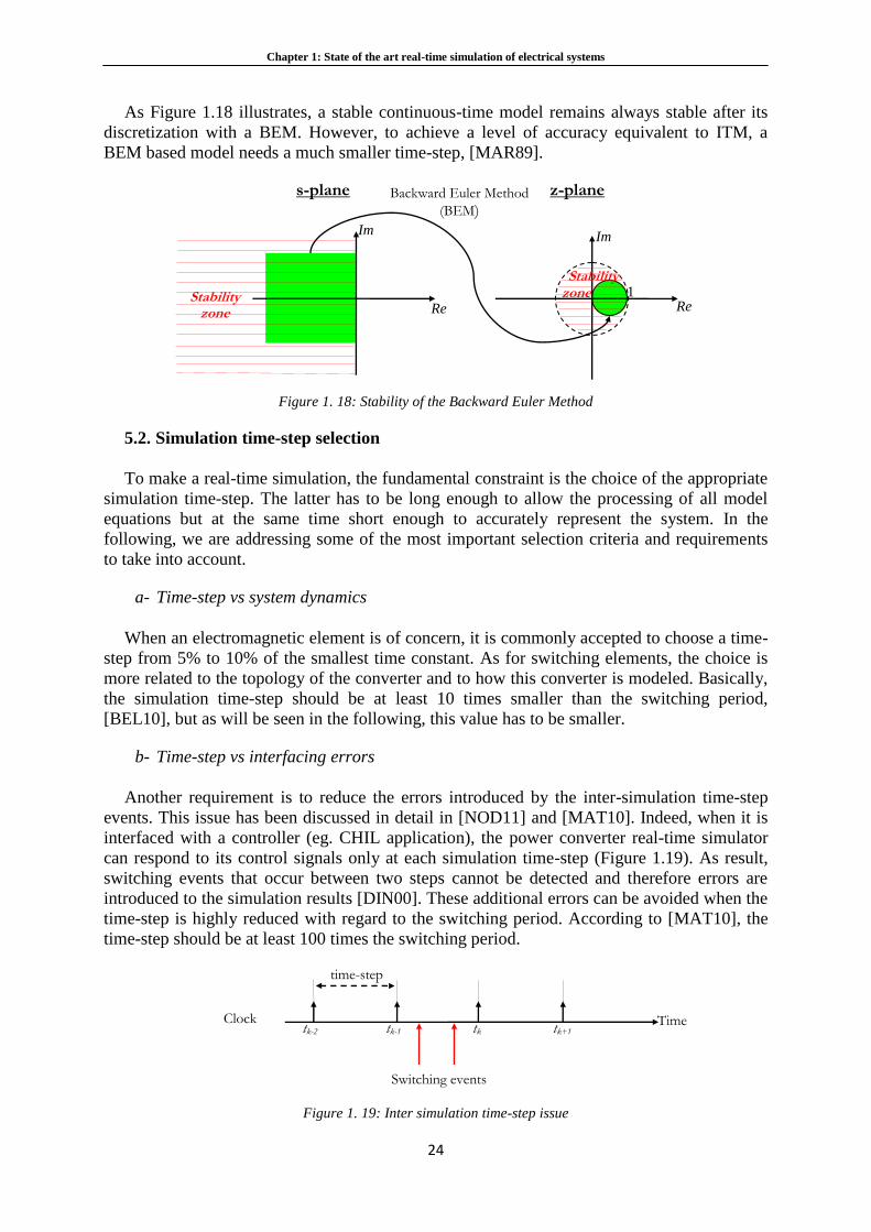
Chapter 1: State of the art real-time simulation of electrical systems
24
As Figure 1.18 illustrates, a stable continuous-time model remains always stable after its
discretization with a BEM. However, to achieve a level of accuracy equivalent to ITM, a
BEM based model needs a much smaller time-step, [MAR89].
Figure 1. 18: Stability of the Backward Euler Method
5.2. Simulation time-step selection
To make a real-time simulation, the fundamental constraint is the choice of the appropriate
simulation time-step. The latter has to be long enough to allow the processing of all model
equations but at the same time short enough to accurately represent the system. In the
following, we are addressing some of the most important selection criteria and requirements
to take into account.
a- Time-step vs system dynamics
When an electromagnetic element is of concern, it is commonly accepted to choose a time-
step from 5% to 10% of the smallest time constant. As for switching elements, the choice is
more related to the topology of the converter and to how this converter is modeled. Basically,
the simulation time-step should be at least 10 times smaller than the switching period,
[BEL10], but as will be seen in the following, this value has to be smaller.
b- Time-step vs interfacing errors
Another requirement is to reduce the errors introduced by the inter-simulation time-step
events. This issue has been discussed in detail in [NOD11] and [MAT10]. Indeed, when it is
interfaced with a controller (eg. CHIL application), the power converter real-time simulator
can respond to its control signals only at each simulation time-step (Figure 1.19). As result,
switching events that occur between two steps cannot be detected and therefore errors are
introduced to the simulation results [DIN00]. These additional errors can be avoided when the
time-step is highly reduced with regard to the switching period. According to [MAT10], the
time-step should be at least 100 times the switching period.
Figure 1. 19: Inter simulation time-step issue
Time tk-2 tk-1 tk tk+1
time-step
Clock
Switching events
Im
Re
1
Im
Re
s-plane z-plane
Stability zone
Backward Euler Method
(BEM)
Stability zone
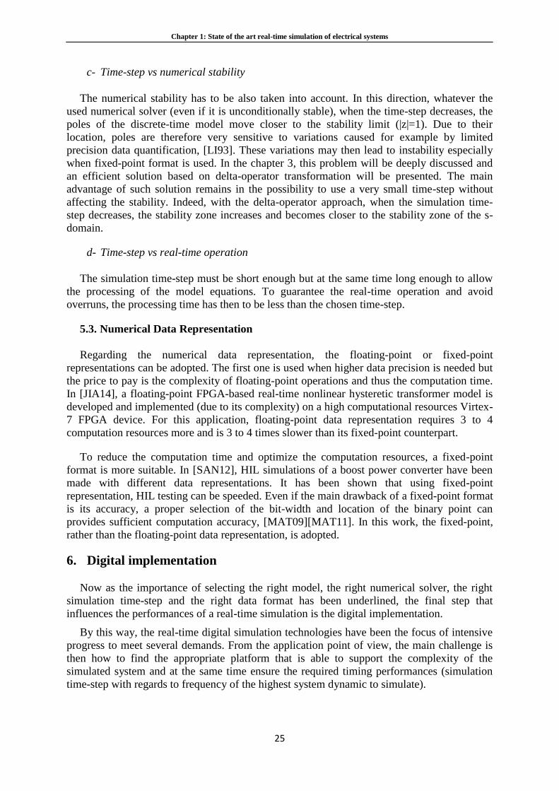
Chapter 1: State of the art real-time simulation of electrical systems
25
c- Time-step vs numerical stability
The numerical stability has to be also taken into account. In this direction, whatever the
used numerical solver (even if it is unconditionally stable), when the time-step decreases, the
poles of the discrete-time model move closer to the stability limit (|z|=1). Due to their
location, poles are therefore very sensitive to variations caused for example by limited
precision data quantification, [LI93]. These variations may then lead to instability especially
when fixed-point format is used. In the chapter 3, this problem will be deeply discussed and
an efficient solution based on delta-operator transformation will be presented. The main
advantage of such solution remains in the possibility to use a very small time-step without
affecting the stability. Indeed, with the delta-operator approach, when the simulation time-
step decreases, the stability zone increases and becomes closer to the stability zone of the s-
domain.
d- Time-step vs real-time operation
The simulation time-step must be short enough but at the same time long enough to allow
the processing of the model equations. To guarantee the real-time operation and avoid
overruns, the processing time has then to be less than the chosen time-step.
5.3. Numerical Data Representation
Regarding the numerical data representation, the floating-point or fixed-point
representations can be adopted. The first one is used when higher data precision is needed but
the price to pay is the complexity of floating-point operations and thus the computation time.
In [JIA14], a floating-point FPGA-based real-time nonlinear hysteretic transformer model is
developed and implemented (due to its complexity) on a high computational resources Virtex-
7 FPGA device. For this application, floating-point data representation requires 3 to 4
computation resources more and is 3 to 4 times slower than its fixed-point counterpart.
To reduce the computation time and optimize the computation resources, a fixed-point
format is more suitable. In [SAN12], HIL simulations of a boost power converter have been
made with different data representations. It has been shown that using fixed-point
representation, HIL testing can be speeded. Even if the main drawback of a fixed-point format
is its accuracy, a proper selection of the bit-width and location of the binary point can
provides sufficient computation accuracy, [MAT09][MAT11]. In this work, the fixed-point,
rather than the floating-point data representation, is adopted.
6. Digital implementation
Now as the importance of selecting the right model, the right numerical solver, the right
simulation time-step and the right data format has been underlined, the final step that
influences the performances of a real-time simulation is the digital implementation.
By this way, the real-time digital simulation technologies have been the focus of intensive
progress to meet several demands. From the application point of view, the main challenge is
then how to find the appropriate platform that is able to support the complexity of the
simulated system and at the same time ensure the required timing performances (simulation
time-step with regards to frequency of the highest system dynamic to simulate).
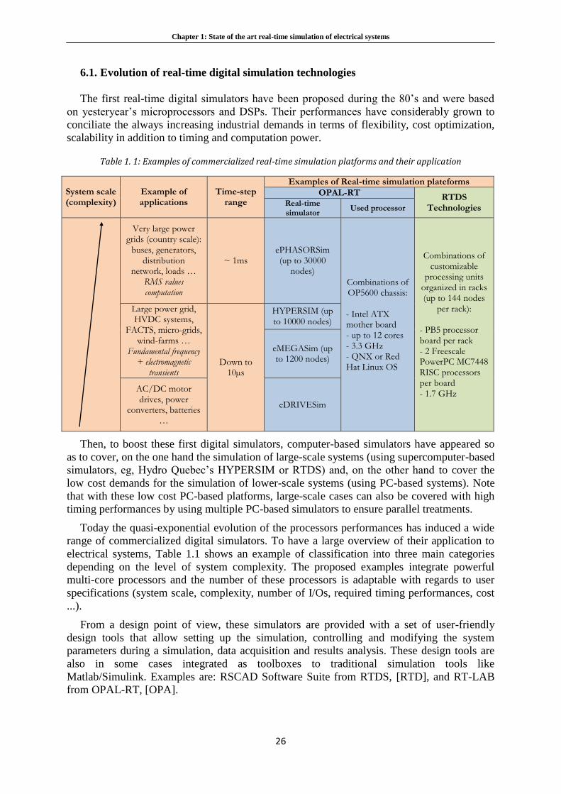
Chapter 1: State of the art real-time simulation of electrical systems
26
6.1. Evolution of real-time digital simulation technologies
The first real-time digital simulators have been proposed during the 80’s and were based
on yesteryear’s microprocessors and DSPs. Their performances have considerably grown to
conciliate the always increasing industrial demands in terms of flexibility, cost optimization,
scalability in addition to timing and computation power.
Table 1. 1: Examples of commercialized real-time simulation platforms and their application
System scale (complexity)
Example of applications
Time-step range
Examples of Real-time simulation plateforms
OPAL-RT RTDS
Technologies Real-time simulator
Used processor
Very large power grids (country scale):
buses, generators, distribution
network, loads … RMS values computation
~ 1ms ePHASORSim (up to 30000
nodes)
Combinations of OP5600 chassis:
- Intel ATX mother board - up to 12 cores - 3.3 GHz - QNX or Red Hat Linux OS
Combinations of customizable
processing units organized in racks (up to 144 nodes
per rack):
- PB5 processor board per rack - 2 Freescale PowerPC MC7448 RISC processors per board - 1.7 GHz
Large power grid, HVDC systems,
FACTS, micro-grids, wind-farms …
Fundamental frequency + electromagnetic
transients Down to
10µs
HYPERSIM (up to 10000 nodes)
eMEGASim (up to 1200 nodes)
AC/DC motor drives, power
converters, batteries …
eDRIVESim
Then, to boost these first digital simulators, computer-based simulators have appeared so
as to cover, on the one hand the simulation of large-scale systems (using supercomputer-based
simulators, eg, Hydro Quebec’s HYPERSIM or RTDS) and, on the other hand to cover the
low cost demands for the simulation of lower-scale systems (using PC-based systems). Note
that with these low cost PC-based platforms, large-scale cases can also be covered with high
timing performances by using multiple PC-based simulators to ensure parallel treatments.
Today the quasi-exponential evolution of the processors performances has induced a wide
range of commercialized digital simulators. To have a large overview of their application to
electrical systems, Table 1.1 shows an example of classification into three main categories
depending on the level of system complexity. The proposed examples integrate powerful
multi-core processors and the number of these processors is adaptable with regards to user
specifications (system scale, complexity, number of I/Os, required timing performances, cost
...).
From a design point of view, these simulators are provided with a set of user-friendly
design tools that allow setting up the simulation, controlling and modifying the system
parameters during a simulation, data acquisition and results analysis. These design tools are
also in some cases integrated as toolboxes to traditional simulation tools like
Matlab/Simulink. Examples are: RSCAD Software Suite from RTDS, [RTD], and RT-LAB
from OPAL-RT, [OPA].
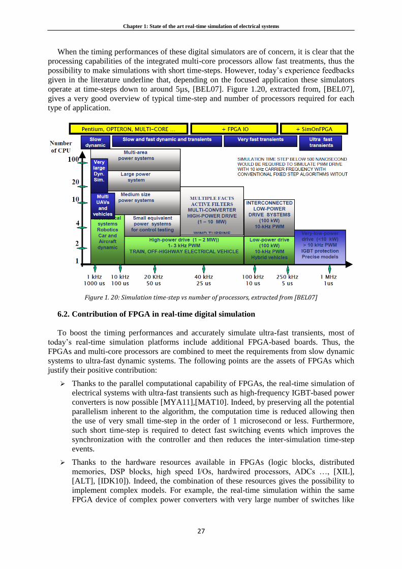
Chapter 1: State of the art real-time simulation of electrical systems
27
When the timing performances of these digital simulators are of concern, it is clear that the
processing capabilities of the integrated multi-core processors allow fast treatments, thus the
possibility to make simulations with short time-steps. However, today’s experience feedbacks
given in the literature underline that, depending on the focused application these simulators
operate at time-steps down to around 5µs, [BEL07]. Figure 1.20, extracted from, [BEL07],
gives a very good overview of typical time-step and number of processors required for each
type of application.
Figure 1. 20: Simulation time-step vs number of processors, extracted from [BEL07]
6.2. Contribution of FPGA in real-time digital simulation
To boost the timing performances and accurately simulate ultra-fast transients, most of
today’s real-time simulation platforms include additional FPGA-based boards. Thus, the
FPGAs and multi-core processors are combined to meet the requirements from slow dynamic
systems to ultra-fast dynamic systems. The following points are the assets of FPGAs which
justify their positive contribution:
Thanks to the parallel computational capability of FPGAs, the real-time simulation of
electrical systems with ultra-fast transients such as high-frequency IGBT-based power
converters is now possible [MYA11],[MAT10]. Indeed, by preserving all the potential
parallelism inherent to the algorithm, the computation time is reduced allowing then
the use of very small time-step in the order of 1 microsecond or less. Furthermore,
such short time-step is required to detect fast switching events which improves the
synchronization with the controller and then reduces the inter-simulation time-step
events.
Thanks to the hardware resources available in FPGAs (logic blocks, distributed
memories, DSP blocks, high speed I/Os, hardwired processors, ADCs …, [XIL],
[ALT], [IDK10]). Indeed, the combination of these resources gives the possibility to
implement complex models. For example, the real-time simulation within the same
FPGA device of complex power converters with very large number of switches like
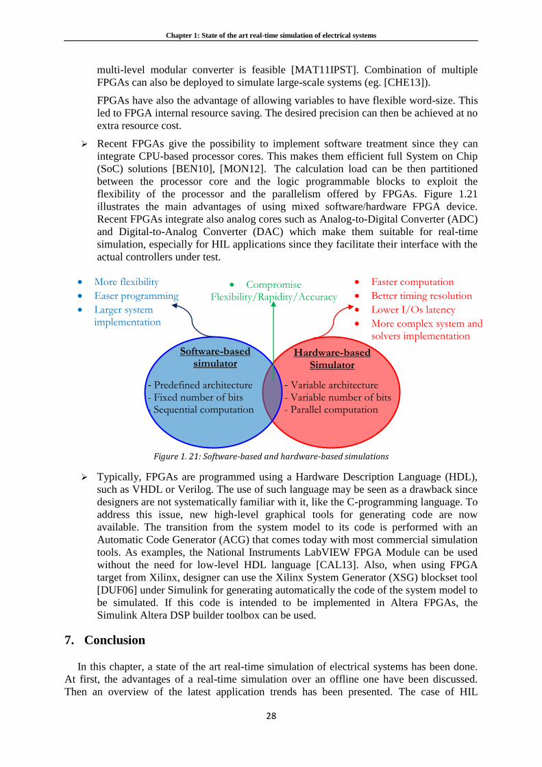
Chapter 1: State of the art real-time simulation of electrical systems
28
multi-level modular converter is feasible [MAT11IPST]. Combination of multiple
FPGAs can also be deployed to simulate large-scale systems (eg. [CHE13]).
FPGAs have also the advantage of allowing variables to have flexible word-size. This
led to FPGA internal resource saving. The desired precision can then be achieved at no
extra resource cost.
Recent FPGAs give the possibility to implement software treatment since they can
integrate CPU-based processor cores. This makes them efficient full System on Chip
(SoC) solutions [BEN10], [MON12]. The calculation load can be then partitioned
between the processor core and the logic programmable blocks to exploit the
flexibility of the processor and the parallelism offered by FPGAs. Figure 1.21
illustrates the main advantages of using mixed software/hardware FPGA device.
Recent FPGAs integrate also analog cores such as Analog-to-Digital Converter (ADC)
and Digital-to-Analog Converter (DAC) which make them suitable for real-time
simulation, especially for HIL applications since they facilitate their interface with the
actual controllers under test.
Figure 1. 21: Software-based and hardware-based simulations
Typically, FPGAs are programmed using a Hardware Description Language (HDL),
such as VHDL or Verilog. The use of such language may be seen as a drawback since
designers are not systematically familiar with it, like the C-programming language. To
address this issue, new high-level graphical tools for generating code are now
available. The transition from the system model to its code is performed with an
Automatic Code Generator (ACG) that comes today with most commercial simulation
tools. As examples, the National Instruments LabVIEW FPGA Module can be used
without the need for low-level HDL language [CAL13]. Also, when using FPGA
target from Xilinx, designer can use the Xilinx System Generator (XSG) blockset tool
[DUF06] under Simulink for generating automatically the code of the system model to
be simulated. If this code is intended to be implemented in Altera FPGAs, the
Simulink Altera DSP builder toolbox can be used.
7. Conclusion
In this chapter, a state of the art real-time simulation of electrical systems has been done.
At first, the advantages of a real-time simulation over an offline one have been discussed.
Then an overview of the latest application trends has been presented. The case of HIL
Hardware-based Simulator
Software-based simulator
Faster computation
Better timing resolution
Lower I/Os latency
More complex system and solvers implementation
- Predefined architecture - Fixed number of bits - Sequential computation
- Variable architecture - Variable number of bits - Parallel computation
More flexibility
Easer programming
Larger system implementation
Compromise Flexibility/Rapidity/Accuracy
Chapter 1: State of the art real-time simulation of electrical systems
29
applications has been focused on. Finally, a deeper discussion about the modeling of electrical
systems, its digital realization and its digital implementation has been made in sections 4.5
and 6.
From this discussion, it is clear that for HIL purposes the main challenge is how to
improve the simulation accuracy and the main constraints are related to the model accuracy
and the simulation time-step. To meet the expected performances, recent real-time simulators
integrate high performance CPU-based boards combined with expensive FPGA boards. In
such HIL applications, the cost is not critical. However, when dealing with embedded real-
time simulation (which is the main topic of this thesis work), the cost becomes very
challenging and the use of low cost devices (FPGAs here) is essential. Then, for a FPGA-
based embedded real-time simulator, a compromise has always to be found between the
expected accuracy of the simulator to reproduce dynamics and transients and the size of the
FPGA on which it will be implemented (size obviously linked to the cost). An efficient
methodology to design FPGA-based embedded real-time simulators for electrical systems is
therefore mandatory.
In the next chapter the FPGA-based embedded real-time simulation of electrical systems
will be discussed and an efficient design methodology will be proposed.
Chapter 2: FPGA-based embedded real-time simulation of electrical Systems
31
Chapter 2
FPGA-based embedded real-time simulation of
electrical systems
Chapter 2: FPGA-based embedded real-time simulation of electrical Systems
32
1. Introduction
We have seen from the previous chapter that the main issue of interest is how to develop
real-time simulators able to accurately reproduce the electrical system dynamics and
transients. To satisfy this, high performance digital simulation platforms are now
commercialized covering a wide range of system complexity and operating at very short
simulation time-steps. At the same time, this high level of performance induces the use of
powerful digital technologies (multi-core processor boards associated with high performance
FPGA boards), which means that the cost of these platforms is not always taken into account.
However, the use of such expensive platforms is not acceptable in the case of embedded
applications where real-time simulator IPs are not only developed for HIL testing but also
embedded within digital controllers. Consequently, the constraints linked to the real-time
simulation (discussed in the former chapter) are strengthened by those of embedded systems
such as cost, power consumption, reliability, size and flexibility.
In this chapter, author starts by discussing the applications where embedded real-time
simulators can be encountered and deals with the benefits of using FPGAs as embedded
digital systems. Then, the induced constraints that must be considered during the development
process are emphasized and organized into five dependent groups. Finally, design guidelines
to be followed in order to manage these constraints are proposed.
2. FPGA-based embedded real-time simulation
2.1. Embedded real-time simulation
As seen in the former chapter, when talking about real-time simulation of electrical
systems, one can systematically put in mind the HIL testing. This is not always the case since
an emerging class of real-time simulators is expected to be more and more included to the
next generation of embedded digital controllers. Then, the development of real-time
simulators in this case must satisfy the real-time simulations constraints highlighted in the
previous chapter and at the same time the constraints linked to the embedded systems.
An embedded real-time simulator can be seen as an IP module that simulates the system to
be controlled or a part of it. Thus, this IP and the controller are both implemented and run
altogether in the same device. The simulator IP is then considered as a part of an embedded
control system. Depending on the way this simulator will be inserted into the control loop and
how it will be connected to the controller and I/O interface, it can play several roles.
First of all, this simulator IP must be usable for HIL testing as illustrated in Figure 2.1.
Then this IP can be included inside the control closed-loop or parallelized with the controller.
When it is included inside the control closed-loop as shown in Figures 2.2 and 2.3, the
simulator plays a crucial role since it influences the control performance. It can be seen as an
observer (estimator) that estimates non measured quantities (currents, voltages, position,
speed...) in the context of sensors reduction (sensorless control, see Figure 2.2), [YIN13],
[PEL12] or in the context of improving the system reliability (fault-tolerant control) by
ensuring a digital system redundancy. The simulator is then activated and inserted in the
control loop in the case of sensor fault, see Figure 2.3), [DEB12]. Another application of
embedded real-time simulators can be the model predictive control, [COR09], [MAR12].
Chapter 2: FPGA-based embedded real-time simulation of electrical Systems
33
Figure 2.1: Embedded real-time simulator IPs applied in the context of HIL validation
Figure 2.2: Embedded real-time simulator IPs included inside the control closed-loop and applied in the context
of sensorless control
Embedded real-time simulator
IPs
Embedded controller I/O Interface
I/O Interface
I/O Interface
Power system
Host-PC
Electromagnetic elements
Switching elements
Control closed-loop
SW1
SW2
SW3 SW4
Digital platform
Embedded real-time simulator
IPs
Embedded controller I/O Interface
I/O Interface
I/O Interface
Power system
Host-PC
Electromagnetic elements
Switching elements
Control closed-loop
SW1
SW2
SW3 SW4
Digital platform
Chapter 2: FPGA-based embedded real-time simulation of electrical Systems
34
Figure 2.3: Embedded real-time simulator IPs included inside the control closed-loop and applied in the context
of fault-tolerant control
The role of the embedded real-time simulator when it is parallelized with the controller is
also of significant interest. In this case, the simulator can play a major role in the context of
real-time fault detection and diagnosis [QUN11], [KAR09], [RAJ13], [DEL11]. It can also be
useful in the context of a health monitoring for preventing unexpected failures and then avoid
unpredictable system downtime [BER12], [ZOE14], [NUS14], [BAB14]. Another application
example could be the estimation in real-time of the conduction and commutation losses of a
power electronic converter. Figure 2.4 presents the principle synoptic of an embedded real-
time simulator parallelized with the controller.
Figure 2.4: Embedded real-time simulator IPs parallelized with the controller and applied in the context of
diagnostic and health-monitoring
Embedded real-time simulator
IPs
Embedded controller I/O Interface
I/O Interface
I/O Interface
Power system
Host-PC
Electromagnetic elements
Switching elements
Control closed-loop
SW1
SW2
SW3 SW4
Digital platform
Supervisor
Embedded
real-time simulator
IPs
Embedded controller I/O
Interface
I/O Interface
I/O Interface
Power system
Host-PC
Electromagnetic elements
Switching elements
Control closed-loop
SW1
SW2
SW3 SW4
Digital platform
Supervisor
Fault
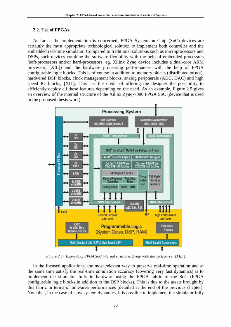
Chapter 2: FPGA-based embedded real-time simulation of electrical Systems
35
2.2. Use of FPGAs
As far as the implementation is concerned, FPGA System on Chip (SoC) devices are
certainly the most appropriate technological solution to implement both controller and the
embedded real-time simulator. Compared to traditional solutions such as microprocessors and
DSPs, such devices combine the software flexibility with the help of embedded processors
(soft-processors and/or hard-processors, eg. Xilinx Zynq device includes a dual-core ARM
processor, [XIL]) and the hardware processing performances with the help of FPGA
configurable logic blocks. This is of course in addition to memory blocks (distributed or not),
hardwired DSP blocks, clock management blocks, analog peripherals (ADC, DAC) and high
speed IO blocks, [XIL]. This has the credit of offering the designer the possibility to
efficiently deploy all these features depending on the need. As an example, Figure 2.5 gives
an overview of the internal structure of the Xilinx Zynq-7000 FPGA SoC (device that is used
in the proposed thesis work).
Figure 2.5: Example of FPGA SoC internal structure: Zynq-7000 device (source: [XIL])
In the focused applications, the most relevant way to preserve real-time operation and at
the same time satisfy the real-time simulation accuracy (covering very fast dynamics) is to
implement the simulator fully in hardware using the FPGA fabric of the SoC (FPGA
configurable logic blocks in addition to the DSP blocks). This is due to the assets brought by
this fabric in terms of time/area performances (detailed at the end of the previous chapter).
Note that, in the case of slow system dynamics, it is possible to implement the simulator fully
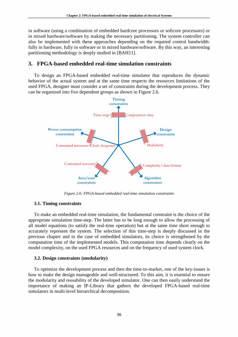
Chapter 2: FPGA-based embedded real-time simulation of electrical Systems
36
in software (using a combination of embedded hardcore processors or softcore processors) or
in mixed hardware/software by making the necessary partitioning. The system controller can
also be implemented with these approaches depending on the required control bandwidth:
fully in hardware, fully in software or in mixed hardware/software. By this way, an interesting
partitioning methodology is deeply studied in [BAH11].
3. FPGA-based embedded real-time simulation constraints
To design an FPGA-based embedded real-time simulator that reproduces the dynamic
behavior of the actual system and at the same time respects the resources limitations of the
used FPGA, designer must consider a set of constraints during the development process. They
can be organized into five dependent groups as shown in Figure 2.6.
Figure 2.6: FPGA-based embedded real-time simulation constraints
3.1. Timing constraints
To make an embedded real-time simulation, the fundamental constraint is the choice of the
appropriate simulation time-step. The latter has to be long enough to allow the processing of
all model equations (to satisfy the real-time operation) but at the same time short enough to
accurately represent the system. The selection of this time-step is deeply discussed in the
previous chapter and in the case of embedded simulators, its choice is strengthened by the
computation time of the implemented models. This computation time depends clearly on the
model complexity, on the used FPGA resources and on the frequency of used system clock.
3.2. Design constraints (modularity)
To optimize the development process and then the time-to-market, one of the key-issues is
how to make the design manageable and well-structured. To this aim, it is essential to ensure
the modularity and reusability of the developed simulator. One can then easily understand the
importance of making an IP-Library that gathers the developed FPGA-based real-time
simulators in multi-level hierarchical decomposition.
Timing constraints
Design constraints
Algorithm constraints
Area/cost constraints
Power consumption constraints
Time-step+
Modularity
Complexity+data format Consumed resources
Consumed resources+
Computation time
Clock frequency
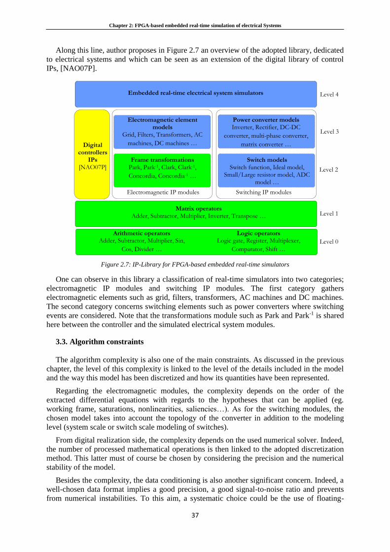
Chapter 2: FPGA-based embedded real-time simulation of electrical Systems
37
Along this line, author proposes in Figure 2.7 an overview of the adopted library, dedicated
to electrical systems and which can be seen as an extension of the digital library of control
IPs, [NAO07P].
Figure 2.7: IP-Library for FPGA-based embedded real-time simulators
One can observe in this library a classification of real-time simulators into two categories;
electromagnetic IP modules and switching IP modules. The first category gathers
electromagnetic elements such as grid, filters, transformers, AC machines and DC machines.
The second category concerns switching elements such as power converters where switching
events are considered. Note that the transformations module such as Park and Park-1 is shared
here between the controller and the simulated electrical system modules.
3.3. Algorithm constraints
The algorithm complexity is also one of the main constraints. As discussed in the previous
chapter, the level of this complexity is linked to the level of the details included in the model
and the way this model has been discretized and how its quantities have been represented.
Regarding the electromagnetic modules, the complexity depends on the order of the
extracted differential equations with regards to the hypotheses that can be applied (eg.
working frame, saturations, nonlinearities, saliencies…). As for the switching modules, the
chosen model takes into account the topology of the converter in addition to the modeling
level (system scale or switch scale modeling of switches).
From digital realization side, the complexity depends on the used numerical solver. Indeed,
the number of processed mathematical operations is then linked to the adopted discretization
method. This latter must of course be chosen by considering the precision and the numerical
stability of the model.
Besides the complexity, the data conditioning is also another significant concern. Indeed, a
well-chosen data format implies a good precision, a good signal-to-noise ratio and prevents
from numerical instabilities. To this aim, a systematic choice could be the use of floating-
Electromagnetic IP modules Switching IP modules
Embedded real-time electrical system simulators
Arithmetic operators Adder, Subtractor, Multiplier, Sin,
Cos, Divider …
Logic operators Logic gate, Register, Multiplexer,
Comparator, Shift …
Matrix operators Adder, Subtractor, Multiplier, Inverter, Transpose …
Frame transformations Park, Park-1, Clark, Clark-1,
Concordia, Concordia-1 …
Switch models
Switch function, Ideal model, Small/Large resistor model, ADC
model …
Electromagnetic element models
Grid, Filters, Transformers, AC
machines, DC machines …
Power converter models Inverter, Rectifier, DC-DC
converter, multi-phase converter,
matrix converter …
Level 0
Level 1
Level 3
Level 4
Level 2
Digital controllers
IPs [NAO07P]
Chapter 2: FPGA-based embedded real-time simulation of electrical Systems
38
point format [BAC13] [JIA14]. Although the latter is well-known for its precision, it presents
limitations especially when using FPGA devices. Indeed, the main challenge is the
complexity of floating-point operators which impacts the FPGA hardware resources and the
total computation time (thus the real-time simulation time-step). That is to say, in some cases,
an optimal choice of fixed-point data format remains an appropriate alternative [SAN12]. In
[GON14], it has been demonstrated that is possible to implement power converter models
using the fixed-point format without loss of precision, while the consumed resources are
minimized and the clock frequency is maximized. This is also confirmed in [SCH14] where a
fixed-point nonlinear permanent magnet synchronous machine model has been compared to
its floating-point counterpart to check the precision and small difference has been obtained.
3.4. Area/Cost constraints
The preservation of the potential parallelism inherent to the algorithm is strongly linked to
the available hardware resources which are limited by the cost of the used FPGA target. The
development of the FPGA architecture must then consider these resources limitation. Another
important concern is the computation time that must be less than the real-time simulation
time-step (to ensure real-time operation). In addition to the latency of the algorithm, this
computation time depends on the used clock frequency. This latter is closely linked to the
quality of the designed architecture and precisely to the propagation delays between the
arithmetic operators. Designer must reduce these delays to increase the maximum achievable
clock frequency and consequently reduce the computation time.
To face this time/area issue and always ensure a low cost FPGA implementation, designer
has to optimize the use of internal resources. At first, the use of hardwired resources such as
DSP units, memory blocks and the integrated processors (when software implementation is
required) must be privileged since they have already been optimized by the device
manufacturer. The pipelining of the architecture is also important to minimize the impact of
the propagation delays. Additionally, one of the interesting techniques to overcome the
resources limitation is to develop a factorized FPGA architecture by adopting the A3
methodology (Algorithm Architecture Adequation) [GRA99]. For a given algorithm
complexity, the objective is the reduction of hardware resources by factorizing heavy
operators (such as multipliers). In contrast, the treatment is locally serialized which may
enlarge the computation time. A compromise must then be established in order to meet the
available resources and the level of factorization with regards to the computation time limit.
3.5. Power consumption constraints
These constraints concern typically applications such as portable and power-conscious
embedded systems where low power consumption is a key-issue. Here again the higher are
the clock frequency and the used hardware resources, the higher is the consumed power. This
point is not maintained in the following discussion since in the case of electrical systems
applications, the power consumption of the digital control unit doesn’t matter compared to the
power consumed by the power system itself.
4. Design guidelines for developing FPGA-based embedded real time
simulators
The proposed design guidelines consist of a set of steps and rules to be followed in order to
get a better compromise between the expected performances of the real-time simulator and the
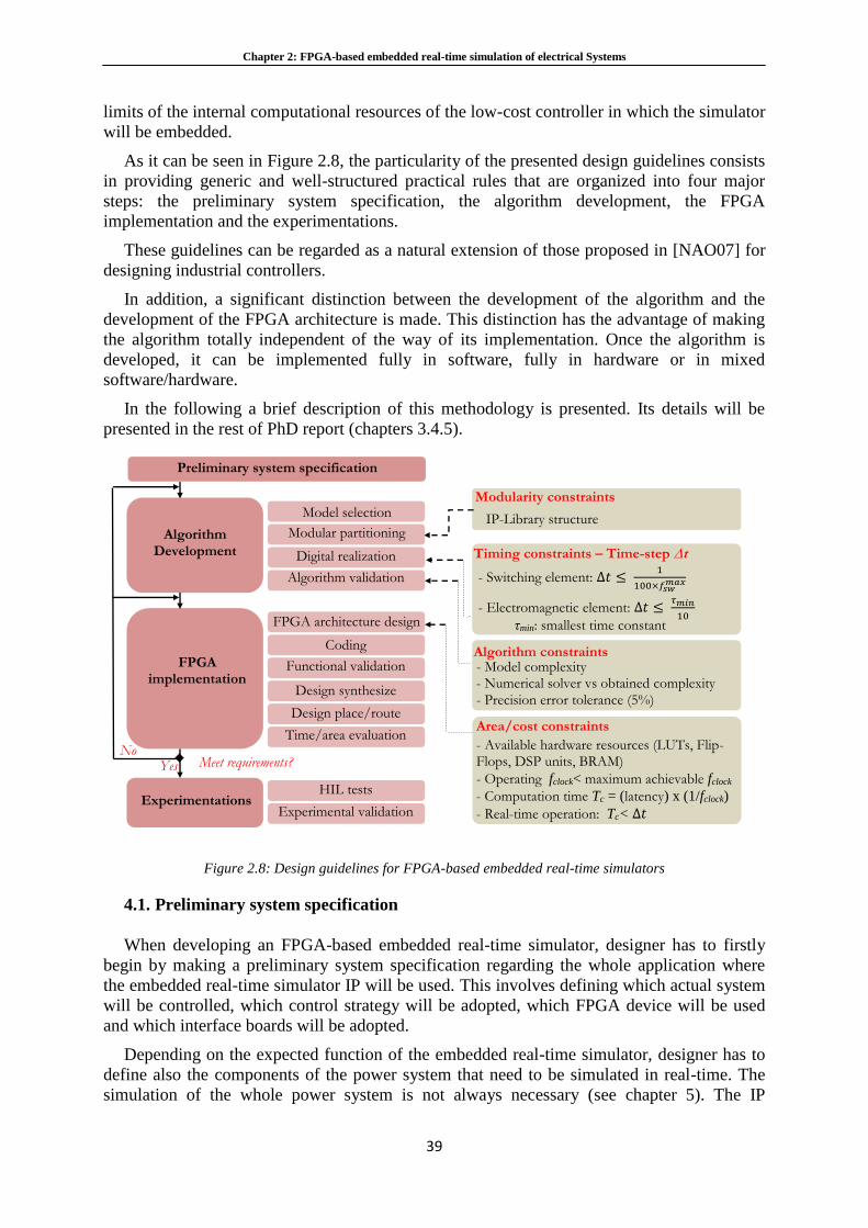
Chapter 2: FPGA-based embedded real-time simulation of electrical Systems
39
limits of the internal computational resources of the low-cost controller in which the simulator
will be embedded.
As it can be seen in Figure 2.8, the particularity of the presented design guidelines consists
in providing generic and well-structured practical rules that are organized into four major
steps: the preliminary system specification, the algorithm development, the FPGA
implementation and the experimentations.
These guidelines can be regarded as a natural extension of those proposed in [NAO07] for
designing industrial controllers.
In addition, a significant distinction between the development of the algorithm and the
development of the FPGA architecture is made. This distinction has the advantage of making
the algorithm totally independent of the way of its implementation. Once the algorithm is
developed, it can be implemented fully in software, fully in hardware or in mixed
software/hardware.
In the following a brief description of this methodology is presented. Its details will be
presented in the rest of PhD report (chapters 3.4.5).
Figure 2.8: Design guidelines for FPGA-based embedded real-time simulators
4.1. Preliminary system specification
When developing an FPGA-based embedded real-time simulator, designer has to firstly
begin by making a preliminary system specification regarding the whole application where
the embedded real-time simulator IP will be used. This involves defining which actual system
will be controlled, which control strategy will be adopted, which FPGA device will be used
and which interface boards will be adopted.
Depending on the expected function of the embedded real-time simulator, designer has to
define also the components of the power system that need to be simulated in real-time. The
simulation of the whole power system is not always necessary (see chapter 5). The IP
Algorithm Development
Meet requirements? Yes No
Modularity constraints
IP-Library structure
Timing constraints – Time-step ∆t
- Switching element: ∆𝑡 ≤ 1
100×𝑓𝑠𝑤𝑚𝑎𝑥
- Electromagnetic element: ∆𝑡 ≤ 𝜏𝑚𝑖𝑛
10
Algorithm constraints - Model complexity - Numerical solver vs obtained complexity - Precision error tolerance (5%)
τmin: smallest time constant
Area/cost constraints
- Available hardware resources (LUTs, Flip-Flops, DSP units, BRAM)
- Operating fclock< maximum achievable fclock
- Computation time Tc = (latency) x (1/fclock)
- Real-time operation: Tc< ∆𝑡
Preliminary system specification
Modular partitioning
Digital realization
Algorithm validation
FPGA implementation
FPGA architecture design
Coding
Functional validation
Design synthesize
Design place/route
Time/area evaluation
Experimentations
HIL tests
Experimental validation
Model selection
Chapter 2: FPGA-based embedded real-time simulation of electrical Systems
40
modules to be used and which have already been developed are then collected from the IP-
Library. Their complexity and time/area performances will be considered during the next
steps.
Defining these components will also lead to deduce the necessary connections and
interfaces between the controller, its embedded real-time simulator and the actual power
system.
4.2. Algorithm development
The algorithm development step is aimed to validate the overall controller including its
embedded real-time simulator with regards to the timing, design and algorithm constraints.
Since the study will be focused only on this simulator, author supposes that the controller
module has already been developed and extracted from the IP-Library.
During this step, the first task consists in choosing the convenient model solver to be
implemented for each element of the electrical system to be simulated. Then, a modular
partitioning is adopted. It consists in dividing each model into independent and reusable
modules. These modules are organized hierarchically with respect to the structure of the
proposed IP-library (see Figure 2.7). Then, a digital version of the simulator algorithm is
derived. During this phase, the simulation time-step is firstly specified based on the timing
constraints imposed by the system (switching frequency of the power converter, time constant
of the electromagnetic elements). This is followed by the selection of the appropriate
numerical solver, the numerical data representation format and the base values for the
normalization, having in mind the implied algorithm constraints.
Finally, an offline simulation is performed using Matlab/Simulink tools. This allows the
verification of the correct functionality of the simulator algorithm when it is included in the
considered control system.
4.3. FPGA Implementation
Once the algorithm development is validated, the designer can start the FPGA
implementation phase. During this phase, the design and validation of the corresponding
FPGA architecture is achieved. Note that for the previously mentioned reasons, a fully
hardware implementation is adopted for the simulator.
To make the design process less constraining, an interesting solution consists in generating
automatically the FPGA-based architecture from Matlab/Simulink, using automatic code
generator [RIC02]. However, this solution is dependent on the performance of this code
generator and can lead to un-optimized architecture that may violate the constraints. This is
why, in the proposed design guidelines, designer has to design, optimize and code himself the
FPGA-based architecture with the help of a set of well-known sub steps but always keeping in
mind the area/cost constraints. The starting point here is the evaluation of the available
hardware resources to be allocated to the simulator IP of concern. Based on that, the
corresponding architecture is developed, coded and included in the whole design.
The hardware architecture of each of the developed modules (according to the adopted
partitioning) is composed of two main parts: a data-path and a control unit. The data-path
contains the used arithmetic or logic operators and data buses between them. The control unit
which is a simple Finite State Machine (FSM) is used for generating a suitable timing
schedule to control the data-path. It is activated via a start pulse signal and generates an End
pulse signal when the computation is completed. The different operational modules are
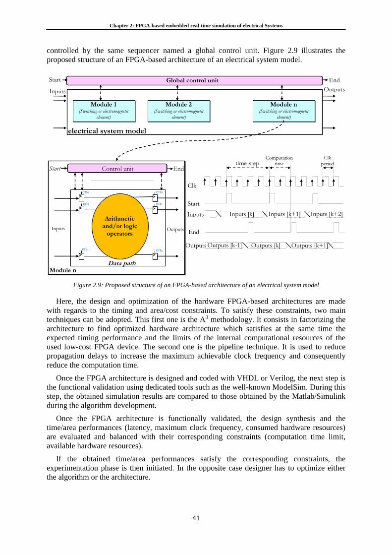
Chapter 2: FPGA-based embedded real-time simulation of electrical Systems
41
controlled by the same sequencer named a global control unit. Figure 2.9 illustrates the
proposed structure of an FPGA-based architecture of an electrical system model.
Figure 2.9: Proposed structure of an FPGA-based architecture of an electrical system model
Here, the design and optimization of the hardware FPGA-based architectures are made
with regards to the timing and area/cost constraints. To satisfy these constraints, two main
techniques can be adopted. This first one is the A3 methodology. It consists in factorizing the
architecture to find optimized hardware architecture which satisfies at the same time the
expected timing performance and the limits of the internal computational resources of the
used low-cost FPGA device. The second one is the pipeline technique. It is used to reduce
propagation delays to increase the maximum achievable clock frequency and consequently
reduce the computation time.
Once the FPGA architecture is designed and coded with VHDL or Verilog, the next step is
the functional validation using dedicated tools such as the well-known ModelSim. During this
step, the obtained simulation results are compared to those obtained by the Matlab/Simulink
during the algorithm development.
Once the FPGA architecture is functionally validated, the design synthesis and the
time/area performances (latency, maximum clock frequency, consumed hardware resources)
are evaluated and balanced with their corresponding constraints (computation time limit,
available hardware resources).
If the obtained time/area performances satisfy the corresponding constraints, the
experimentation phase is then initiated. In the opposite case designer has to optimize either
the algorithm or the architecture.
Global control unit
electrical system model
Module 1 (Switching or electromagnetic
element)
Module 2 (Switching or electromagnetic
element)
Module n (Switching or electromagnetic
element)
End
Inputs Outputs
Start
Control unit Start End
Module n Data path
en0
en1
enn
en0
en1
enn
Arithmetic and/or logic
operators
Start
Inputs
End
Outputs
Clk
Inputs [k] Inputs [k+1] Inputs [k+2]
Outputs [k] Outputs [k+1] Outputs [k-1]
Inputs Outputs
time-step Computation
time
Clk period
Chapter 2: FPGA-based embedded real-time simulation of electrical Systems
42
4.4. Experimentations
The last step aims to make experimental validations starting with HIL tests where the
association and interaction between the controller and its embedded real-time simulator are
tested, and ending by a full experimental validation using the experimental platform.
5. Conclusion
In this chapter, a state of the art FPGA-based embedded real-time simulation of electrical
systems has been done. At first, the applications where embedded real-time simulators can be
encountered have been discussed. Then, the benefits of using FPGAs as embedded digital
systems have been presented. The most important constraints linked to the FPGA-based
embedded real-time simulators have been then emphasized. Also, design guidelines to be
followed in order to manage these constraints during the development process have been
proposed.
In the next chapter the implementation in low-cost FPGA of embedded real-time simulator
IPs of electromagnetic elements of an electrical system will be discussed and the proposed
guidelines will be adopted.
Chapter 3: Implementation in low cost FPGA of embedded real-time simulator IPs of electromagnetic elements
43
Chapter 3
Implementation in low cost FPGA of embedded real-
time simulator IPs of electromagnetic elements
Chapter 3: Implementation in low cost FPGA of embedded real-time simulator IPs of electromagnetic elements
44
1. Introduction
As we have seen in the previous chapter, making an IP-library devoted to embedded real-
time simulator IPs is of great importance to ensure their modularity and reusability. In the
proposed IP-library, these modules are classified into two main categories; those dedicated to
electromagnetic systems (including moving systems) and those dedicated to switching
systems.
In this chapter the first category is focused on. Three cases have been studied: the
embedded real-time simulator of a 3-phase DC-excited synchronous machine, the one of a 3-
phase induction machine and finally the one of a three-stage avionics alternator. As a recall,
application examples of these IPs have been discussed in the previous chapter.
The main challenge when developing an FPGA-based embedded real-time simulator is
how to accurately simulate the system dynamics (electrical dynamics, mechanical dynamics
and possibly thermal dynamics), generally described by differential equations, but having
always in mind the timing, the algorithm and the area/cost constraints. This is the reason why
the proposed design guidelines have been applied to the chosen case studies.
Furthermore, during the digital realization of the synchronous machine simulator IP, the
benefits of making a delta transformation is discussed. Indeed, compared to a shift operator,
this transformation aims to improve the stability of the numerical solver when short
simulation time-step and fixed-point (with limited data precision) are used.
2. FPGA-based embedded real-time simulator of a 3-phase DC-excited
synchronous machine
In this section, the development of an FPGA-based embedded real-time simulator IP of a
synchronous machine is dealt with. This development has been presented and structured
according to the proposed design guidelines.
2.1. Preliminary system specification
The chosen 3-phase DC-excited synchronous machine is a wound-rotor, Y-connected and
salient machine. Its parameters are listed below:
Table 3. 1: Synchronous Machine Parameters
0.8 KVA, 230V, 50 Hz, 3 Phases, Y connection
Stator resistance
Rs= 10.5 Ω
Rotor resistance
Rr= 62.5 Ω
d axis stator inductance
Lsd = 0.245 H
Mutual inductance
Msr= 0.85 H
q axis stator inductance
Lsq= 0.229 H
Nominal stator current
Isn= 1.52 A
Rotor inertia
J=0.0006 Kg.m²
Viscous friction coefficient
f=0.05 Kg.m²/s
Number of pole pairs
p =2
Excitation current
Ird=1.5 A
The machine simulator IP has to be reusable for a wide range of powers and for different
structures. To make a complete validation, this simulator is associated to the IP of a 3-phase
2-level inverter (studied in chapter 4) and the one of a mechanical load. Also an ON-OFF
Chapter 3: Implementation in low cost FPGA of embedded real-time simulator IPs of electromagnetic elements
45
hysteresis stator current controller is used, [NAO07P]. All these IPs are implemented in the
same Xilinx XC7Z020 Zynq device [XIL]. Also, it should be noted that in the following, the
developed synchronous machine simulator IP has been applied in the context of HIL
validation (see Figure 2.1, chapter 2).
2.2. Algorithm development
a- Model selection
To start with, the d-q based model with external Park transformations has been chosen. As
investigated in the first chapter, this model allows reducing the number of equations and their
complexity but at the same time allows reaching an acceptable level of accuracy. These
characteristics are very important in the context of this work since they can contribute to find
the best compromise between the timing and area/cost constraints.
The proposed model assumes that the saturations, the core losses and the skin effects are
neglected. Moreover, it is assumed that rotor excitation current is kept constant (see Table
3.1). The state-space continuous-time model is described by the following equations (relations
3.1 and 3.2).The latter are expressed in rotor reference frame (d-q coordinates, with d-axis
linked to the inductor).
𝑠. 𝑖𝑠𝑑 = −
𝑅𝑠𝐿𝑠𝑑
. 𝑖𝑠𝑑 +𝐿𝑠𝑞
𝐿𝑠𝑑. 𝜔𝑒 . 𝑖𝑠𝑞 +
1
𝐿𝑠𝑑. 𝑣𝑠𝑑
𝑠. 𝑖𝑠𝑞 = −𝐿𝑠𝑑𝐿𝑠𝑞
. 𝜔𝑒 . 𝑖𝑠𝑑 −𝑅𝑠𝐿𝑠𝑞
. 𝑖𝑠𝑞 −𝑀𝑠𝑟
𝐿𝑠𝑞. 𝐼𝑟𝑑 +
1
𝐿𝑠𝑞. 𝑣𝑠𝑞
(3.1)
𝑠. 𝜔𝑒 = −
3
2.𝑝2
𝐽([𝐿𝑠𝑑 − 𝐿𝑠𝑞]. 𝑖𝑠𝑑. 𝑖𝑠𝑞 +𝑀𝑠𝑟 . 𝐼𝑟𝑑. 𝑖𝑠𝑞) −
𝑓
𝐽. 𝜔𝑒 −
𝑝
𝐽. 𝑇𝐿
𝑠. 𝜃𝑒 = 𝜔𝑒
(3.2)
The expression of the electromagnetic torque Te is given in relation 3.3. In our case, the
modelled synchronous machine is salient (Lsd<Lsq).
𝑇𝑒 =3
2. 𝑝. [𝐿𝑠𝑑 − 𝐿𝑠𝑞]. 𝑖𝑠𝑑 . 𝑖𝑠𝑞 +
3
2. 𝑝.𝑀𝑠𝑟 . 𝐼𝑟𝑑. 𝑖𝑠𝑞 (3.3)
b- Modular partitioning
The selected model has been partitioned with respect to the structure of the proposed IP-
Library. To this aim, the d-q based synchronous machine model is divided into three
independent and reusable modules (Figure 3.1): the Park transformation (abc-dq), the
machine model (electrical and mechanical models) and the Park-1 transformation (dq-abc).
Figure 3.1 highlights the interconnections between these modules.
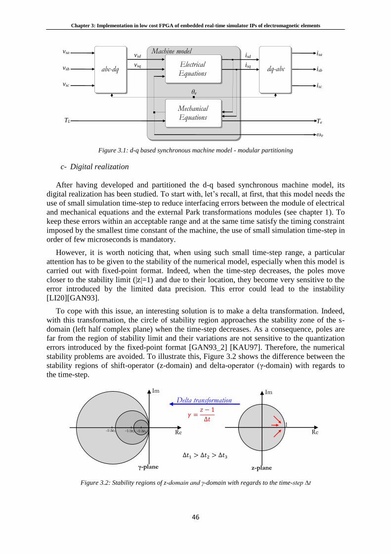
Chapter 3: Implementation in low cost FPGA of embedded real-time simulator IPs of electromagnetic elements
46
Figure 3.1: d-q based synchronous machine model - modular partitioning
c- Digital realization
After having developed and partitioned the d-q based synchronous machine model, its
digital realization has been studied. To start with, let’s recall, at first, that this model needs the
use of small simulation time-step to reduce interfacing errors between the module of electrical
and mechanical equations and the external Park transformations modules (see chapter 1). To
keep these errors within an acceptable range and at the same time satisfy the timing constraint
imposed by the smallest time constant of the machine, the use of small simulation time-step in
order of few microseconds is mandatory.
However, it is worth noticing that, when using such small time-step range, a particular
attention has to be given to the stability of the numerical model, especially when this model is
carried out with fixed-point format. Indeed, when the time-step decreases, the poles move
closer to the stability limit (|z|=1) and due to their location, they become very sensitive to the
error introduced by the limited data precision. This error could lead to the instability
[LI20][GAN93].
To cope with this issue, an interesting solution is to make a delta transformation. Indeed,
with this transformation, the circle of stability region approaches the stability zone of the s-
domain (left half complex plane) when the time-step decreases. As a consequence, poles are
far from the region of stability limit and their variations are not sensitive to the quantization
errors introduced by the fixed-point format [GAN93_2] [KAU97]. Therefore, the numerical
stability problems are avoided. To illustrate this, Figure 3.2 shows the difference between the
stability regions of shift-operator (z-domain) and delta-operator (γ-domain) with regards to
the time-step.
Figure 3.2: Stability regions of z-domain and γ-domain with regards to the time-step ∆t
Im Im
Re Re
γ-plane z-plane
-1/∆t1 -1/∆t2 -1/∆t3
𝛾 =𝑧 − 1
∆𝑡
Delta transformation
∆𝑡1 > ∆𝑡2 > ∆𝑡3
1
abc-dq dq-abc Electrical Equations
Mechanical Equations
Machine model
isb
isc
vsa
vsb
vsc
vsd
vsq
isd
isq
Te TL
θe
ωe
isa
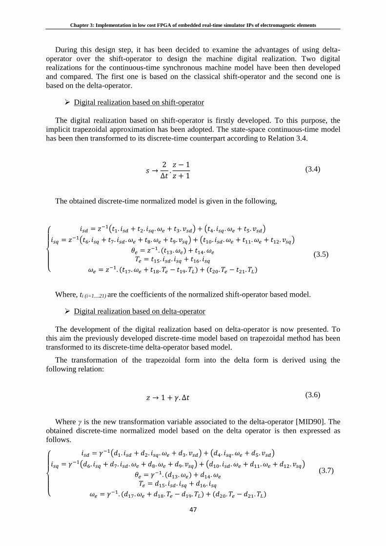
Chapter 3: Implementation in low cost FPGA of embedded real-time simulator IPs of electromagnetic elements
47
During this design step, it has been decided to examine the advantages of using delta-
operator over the shift-operator to design the machine digital realization. Two digital
realizations for the continuous-time synchronous machine model have been then developed
and compared. The first one is based on the classical shift-operator and the second one is
based on the delta-operator.
Digital realization based on shift-operator
The digital realization based on shift-operator is firstly developed. To this purpose, the
implicit trapezoidal approximation has been adopted. The state-space continuous-time model
has been then transformed to its discrete-time counterpart according to Relation 3.4.
𝑠 →2
∆𝑡.𝑧 − 1
𝑧 + 1 (3.4)
The obtained discrete-time normalized model is given in the following,
𝑖𝑠𝑑 = 𝑧−1(𝑡1. 𝑖𝑠𝑑 + 𝑡2. 𝑖𝑠𝑞 . 𝜔𝑒 + 𝑡3. 𝑣𝑠𝑑) + (𝑡4. 𝑖𝑠𝑞 . 𝜔𝑒 + 𝑡5. 𝑣𝑠𝑑)
𝑖𝑠𝑞 = 𝑧−1(𝑡6. 𝑖𝑠𝑞 + 𝑡7. 𝑖𝑠𝑑 . 𝜔𝑒 + 𝑡8. 𝜔𝑒 + 𝑡9. 𝑣𝑠𝑞) + (𝑡10. 𝑖𝑠𝑑 . 𝜔𝑒 + 𝑡11. 𝜔𝑒 + 𝑡12. 𝑣𝑠𝑞)
𝜃𝑒 = 𝑧−1. (𝑡13. 𝜔𝑒) + 𝑡14. 𝜔𝑒
𝑇𝑒 = 𝑡15. 𝑖𝑠𝑑 . 𝑖𝑠𝑞 + 𝑡16. 𝑖𝑠𝑞
𝜔𝑒 = 𝑧−1. (𝑡17. 𝜔𝑒 + 𝑡18. 𝑇𝑒 − 𝑡19. 𝑇𝐿) + (𝑡20. 𝑇𝑒 − 𝑡21. 𝑇𝐿)
(3.5)
Where, ti (i=1....21) are the coefficients of the normalized shift-operator based model.
Digital realization based on delta-operator
The development of the digital realization based on delta-operator is now presented. To
this aim the previously developed discrete-time model based on trapezoidal method has been
transformed to its discrete-time delta-operator based model.
The transformation of the trapezoidal form into the delta form is derived using the
following relation:
𝑧 → 1 + 𝛾. ∆𝑡 (3.6)
Where γ is the new transformation variable associated to the delta-operator [MID90]. The
obtained discrete-time normalized model based on the delta operator is then expressed as
follows.
𝑖𝑠𝑑 = 𝛾−1(𝑑1. 𝑖𝑠𝑑 + 𝑑2. 𝑖𝑠𝑞 . 𝜔𝑒 + 𝑑3. 𝑣𝑠𝑑) + (𝑑4. 𝑖𝑠𝑞 . 𝜔𝑒 + 𝑑5. 𝑣𝑠𝑑)
𝑖𝑠𝑞 = 𝛾−1(𝑑6. 𝑖𝑠𝑞 + 𝑑7. 𝑖𝑠𝑑 . 𝜔𝑒 + 𝑑8. 𝜔𝑒 + 𝑑9. 𝑣𝑠𝑞) + (𝑑10. 𝑖𝑠𝑑 . 𝜔𝑒 + 𝑑11. 𝜔𝑒 + 𝑑12. 𝑣𝑠𝑞)
𝜃𝑒 = 𝛾−1. (𝑑13. 𝜔𝑒) + 𝑑14. 𝜔𝑒
𝑇𝑒 = 𝑑15. 𝑖𝑠𝑑 . 𝑖𝑠𝑞 + 𝑑16. 𝑖𝑠𝑞
𝜔𝑒 = 𝛾−1. (𝑑17. 𝜔𝑒 + 𝑑18. 𝑇𝑒 − 𝑑19. 𝑇𝐿) + (𝑑20. 𝑇𝑒 − 𝑑21. 𝑇𝐿)
(3.7)
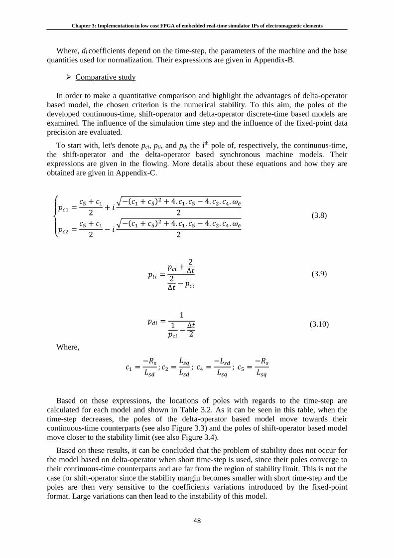
Chapter 3: Implementation in low cost FPGA of embedded real-time simulator IPs of electromagnetic elements
48
Where, di coefficients depend on the time-step, the parameters of the machine and the base
quantities used for normalization. Their expressions are given in Appendix-B.
Comparative study
In order to make a quantitative comparison and highlight the advantages of delta-operator
based model, the chosen criterion is the numerical stability. To this aim, the poles of the
developed continuous-time, shift-operator and delta-operator discrete-time based models are
examined. The influence of the simulation time step and the influence of the fixed-point data
precision are evaluated.
To start with, let's denote pci, pti, and pdi the ith pole of, respectively, the continuous-time,
the shift-operator and the delta-operator based synchronous machine models. Their
expressions are given in the flowing. More details about these equations and how they are
obtained are given in Appendix-C.
𝑝𝑐1 =
𝑐5 + 𝑐12
+ 𝑖√−(𝑐1 + 𝑐5)2 + 4. 𝑐1. 𝑐5 − 4. 𝑐2. 𝑐4. 𝜔𝑒
2
𝑝𝑐2 =𝑐5 + 𝑐12
− 𝑖√−(𝑐1 + 𝑐5)2 + 4. 𝑐1. 𝑐5 − 4. 𝑐2. 𝑐4. 𝜔𝑒
2
(3.8)
𝑝𝑡𝑖 =𝑝𝑐𝑖 +
2∆𝑡
2∆𝑡 − 𝑝𝑐𝑖
(3.9)
𝑝𝑑𝑖 =1
1𝑝𝑐𝑖
−∆𝑡2
(3.10)
Where,
𝑐1 =−𝑅𝑠𝐿𝑠𝑑
; 𝑐2 =𝐿𝑠𝑞
𝐿𝑠𝑑; 𝑐4 =
−𝐿𝑠𝑑𝐿𝑠𝑞
; 𝑐5 =−𝑅𝑠𝐿𝑠𝑞
Based on these expressions, the locations of poles with regards to the time-step are
calculated for each model and shown in Table 3.2. As it can be seen in this table, when the
time-step decreases, the poles of the delta-operator based model move towards their
continuous-time counterparts (see also Figure 3.3) and the poles of shift-operator based model
move closer to the stability limit (see also Figure 3.4).
Based on these results, it can be concluded that the problem of stability does not occur for
the model based on delta-operator when short time-step is used, since their poles converge to
their continuous-time counterparts and are far from the region of stability limit. This is not the
case for shift-operator since the stability margin becomes smaller with short time-step and the
poles are then very sensitive to the coefficients variations introduced by the fixed-point
format. Large variations can then lead to the instability of this model.
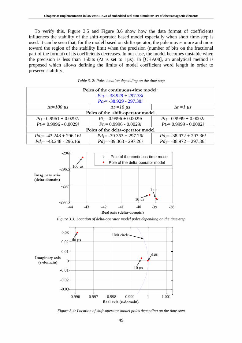
Chapter 3: Implementation in low cost FPGA of embedded real-time simulator IPs of electromagnetic elements
49
To verify this, Figure 3.5 and Figure 3.6 show how the data format of coefficients
influences the stability of the shift-operator based model especially when short time-step is
used. It can be seen that, for the model based on shift-operator, the pole moves more and more
toward the region of the stability limit when the precision (number of bits on the fractional
part of the format) of its coefficients decreases. In our case, the model becomes unstable when
the precision is less than 15bits (∆t is set to 1µs). In [CHA08], an analytical method is
proposed which allows defining the limits of model coefficient word length in order to
preserve stability.
Table 3. 2: Poles location depending on the time-step
Poles of the continuous-time model:
Pc1= -38.929 + 297.38i
Pc2= -38.929 - 297.38i
∆t=100 µs ∆t =10 µs ∆t =1 µs
Poles of the shift-operator model
Pt1= 0.9961 + 0.0297i
Pt2= 0.9996 - 0.0029i
Pt1= 0.9996 + 0.0029i
Pt2= 0.9996 - 0.0029i
Pt1= 0.9999 + 0.0002i
Pt2= 0.9999 - 0.0002i
Poles of the delta-operator model
Pd1= -43.248 + 296.16i
Pd2= -43.248 - 296.16i
Pd1= -39.363 + 297.26i
Pd2= -39.363 - 297.26i
Pd1= -38.972 + 297.36i
Pd2= -38.972 – 297.36i
Figure 3.3: Location of delta-operator model poles depending on the time-step
Figure 3.4: Location of shift-operator model poles depending on the time-step
0.996 0.997 0.998 0.999 1 1.001
-0.03
-0.02
-0.01
0
0.01
0.02
0.03
0.996 0.997 0.998 0.999 1 1.001
-0.03
-0.02
-0.01
0.03
0.02
0.01
0
100 µs
10 µs
1µs
Unit circle
Real axis (z-domain)
Imaginary axis (z-domain)
-44 -43 -42 -41 -40 -39 -38-297.5
-297
-296.5
-296
-38.99 -38.98 -38.97 -38.96 -38.95 -38.94 -38.93 -38.92-297.38
-297.375
-297.37
-297.365
Pole of the continous-time model
Pole of the delta operator model
-44 -43 -42 -41 -40 -38
-297.5
-297
-296.5
-296
-39
Real axis (delta-domain)
Imaginary axis (delta-domain)
1 µs
10 µs
100 µs
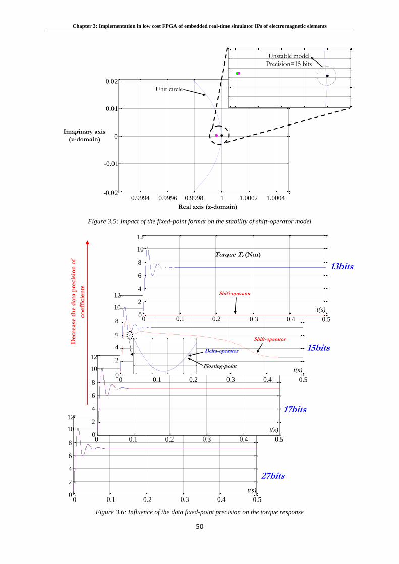
Chapter 3: Implementation in low cost FPGA of embedded real-time simulator IPs of electromagnetic elements
50
Figure 3.5: Impact of the fixed-point format on the stability of shift-operator model
Figure 3.6: Influence of the data fixed-point precision on the torque response
0 0.1 0.2 0.3 0.4 0.50
2
4
6
8
10
12
0 0.1 0.2 0.3 0.4 0.50
2
4
6
8
10
12
0 0.1 0.2 0.3 0.4 0.50
2
4
6
8
10
12
0 0.1 0.2 0.3 0.4 0.50
2
4
6
8
10
12
0 0.1 0.2 0.3 0.4 0.5 0
t(s)
2
4
8 0 0.1 0.2 0.3 0.4 0.5
t(s)
0 0.1 0.2 0.3 0.4 0.5
t(s)
0 0.1 0.2 0.3 0.4 0.5
t(s)
27bits
17bits
15bits
13bits
Torque Te (Nm)
Shift-operator
6
10
12
0
2
4
8
6
10
12
0
2
4
8
6
10
12
0
2
4
8
6
10
12
0.024 0.026 0.028 0.03
6
6.2
6.4
Delta-operator
Floating-point
Shift-operator
Decre
ase
th
e d
ata
pre
cis
ion
of
co
eff
icie
nts
0.9994 0.9996 0.9998 1 1.0002 1.0004-0.02
-0.01
0
0.01
0.02
-0.02 0.9994 0.9996 0.9998 1 1.0002 1.0004
-0.01
0
0.01
0.02
1 1 1 1 1 1-4
-2
0
2
4
6
8x 10
-4
Real axis (z-domain)
Imaginary axis (z-domain)
Unit circle
Unstable model
Precision=15 bits
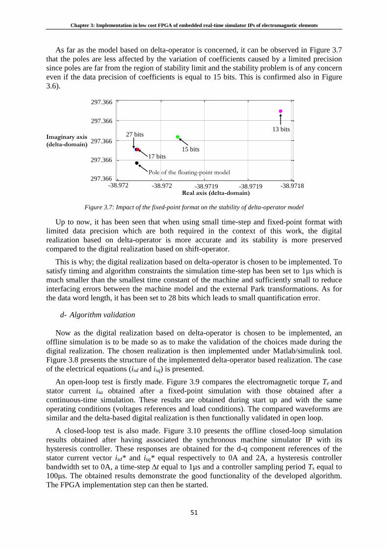
Chapter 3: Implementation in low cost FPGA of embedded real-time simulator IPs of electromagnetic elements
51
As far as the model based on delta-operator is concerned, it can be observed in Figure 3.7
that the poles are less affected by the variation of coefficients caused by a limited precision
since poles are far from the region of stability limit and the stability problem is of any concern
even if the data precision of coefficients is equal to 15 bits. This is confirmed also in Figure
3.6).
Figure 3.7: Impact of the fixed-point format on the stability of delta-operator model
Up to now, it has been seen that when using small time-step and fixed-point format with
limited data precision which are both required in the context of this work, the digital
realization based on delta-operator is more accurate and its stability is more preserved
compared to the digital realization based on shift-operator.
This is why; the digital realization based on delta-operator is chosen to be implemented. To
satisfy timing and algorithm constraints the simulation time-step has been set to 1µs which is
much smaller than the smallest time constant of the machine and sufficiently small to reduce
interfacing errors between the machine model and the external Park transformations. As for
the data word length, it has been set to 28 bits which leads to small quantification error.
d- Algorithm validation
Now as the digital realization based on delta-operator is chosen to be implemented, an
offline simulation is to be made so as to make the validation of the choices made during the
digital realization. The chosen realization is then implemented under Matlab/simulink tool.
Figure 3.8 presents the structure of the implemented delta-operator based realization. The case
of the electrical equations (isd and isq) is presented.
An open-loop test is firstly made. Figure 3.9 compares the electromagnetic torque Te and
stator current isa obtained after a fixed-point simulation with those obtained after a
continuous-time simulation. These results are obtained during start up and with the same
operating conditions (voltages references and load conditions). The compared waveforms are
similar and the delta-based digital realization is then functionally validated in open loop.
A closed-loop test is also made. Figure 3.10 presents the offline closed-loop simulation
results obtained after having associated the synchronous machine simulator IP with its
hysteresis controller. These responses are obtained for the d-q component references of the
stator current vector isd* and isq* equal respectively to 0A and 2A, a hysteresis controller
bandwidth set to 0A, a time-step ∆t equal to 1µs and a controller sampling period Ts equal to
100μs. The obtained results demonstrate the good functionality of the developed algorithm.
The FPGA implementation step can then be started.
-38.972 -38.972 -38.9719 -38.9719 -38.9718297.3666
297.3666
297.3666
297.3666
297.3666
-38.972
-38.972
-38.9719
-38.9719
-38.9718
297.366
297.366
297.366
297.366
297.366
13 bits
15 bits 17 bits
27 bits Imaginary axis (delta-domain)
Real axis (delta-domain)
Pole of the floating-point model
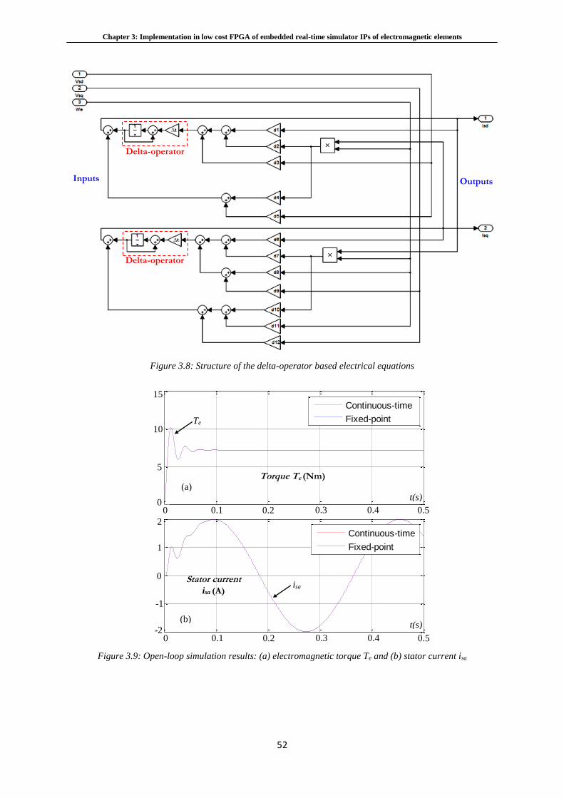
Chapter 3: Implementation in low cost FPGA of embedded real-time simulator IPs of electromagnetic elements
52
Figure 3.8: Structure of the delta-operator based electrical equations
Figure 3.9: Open-loop simulation results: (a) electromagnetic torque Te and (b) stator current isa
0 0.1 0.2 0.3 0.4 0.50
5
10
15
Continuous-time
Fixed-point
0 0.1 0.2 0.3 0.4 0.5
5
10
15
0
0 0.1 0.2 0.3 0.4 0.5-2
-1
0
1
2
Continuous-time
Fixed-point
0 0.1 0.2 0.3 0.4 0.5
0
1
2
-1
-2
(a)
(b)
Te
isa
t(s)
t(s)
Torque Te (Nm)
Stator current
isa (A)
Delta-operator
Delta-operator
Inputs
∆t
∆t
Outputs
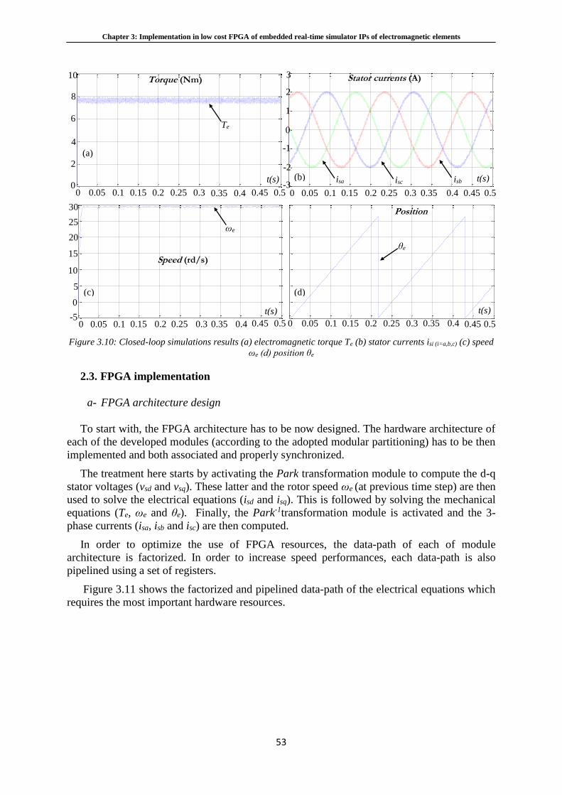
Chapter 3: Implementation in low cost FPGA of embedded real-time simulator IPs of electromagnetic elements
53
Figure 3.10: Closed-loop simulations results (a) electromagnetic torque Te (b) stator currents isi (i=a,b,c) (c) speed
ωe (d) position θe
2.3. FPGA implementation
a- FPGA architecture design
To start with, the FPGA architecture has to be now designed. The hardware architecture of
each of the developed modules (according to the adopted modular partitioning) has to be then
implemented and both associated and properly synchronized.
The treatment here starts by activating the Park transformation module to compute the d-q
stator voltages (vsd and vsq). These latter and the rotor speed ωe (at previous time step) are then
used to solve the electrical equations (isd and isq). This is followed by solving the mechanical
equations (Te, ωe and θe). Finally, the Park-1transformation module is activated and the 3-
phase currents (isa, isb and isc) are then computed.
In order to optimize the use of FPGA resources, the data-path of each of module
architecture is factorized. In order to increase speed performances, each data-path is also
pipelined using a set of registers.
Figure 3.11 shows the factorized and pipelined data-path of the electrical equations which
requires the most important hardware resources.
0 0.05 0.1 0.15 0.2 0.25 0.3 0.35 0.4 0.45 0.50
2
4
6
8
10
0 0.05 0.1 0.15 0.2 0.25 0.3 0.35 0.4 0.45 0.5-5
0
5
10
15
20
25
30
0.05 0.1 0.15 0.2 0.25 0.3 0.35 0.4 0.45 0.5 0 0.05 0.1 0.15 0.2 0.25 0.3 0.35 0.4 0.45 0.5-3
-2
-1
0
1
2
3
0
2
4
0
6
8
0.05 0.1 0.15 0.2 0.25 0.3 0.35 0.4 0.45 0
10
-3
-2
-1
0
1
2
3
5
10
-5
15
20
25
0
30
0.05 0.1 0.15 0.2 0.25 0.3 0.35 0.4 0.45 0.5 0
0.5
0 0.05 0.1 0.15 0.2 0.25 0.3 0.35 0.4 0.45 0.50
1
2
3
4
5
6
7
0.05 0.1 0.15 0.2 0.25 0.3 0.35 0.4 0.45 0 0.5
(a)
(b)
(c) (d)
Te
ωe
θe
isa isc isb t(s)
t(s) t(s)
t(s)
Stator currents (A) Torque (Nm)
Speed (rd/s)
Position
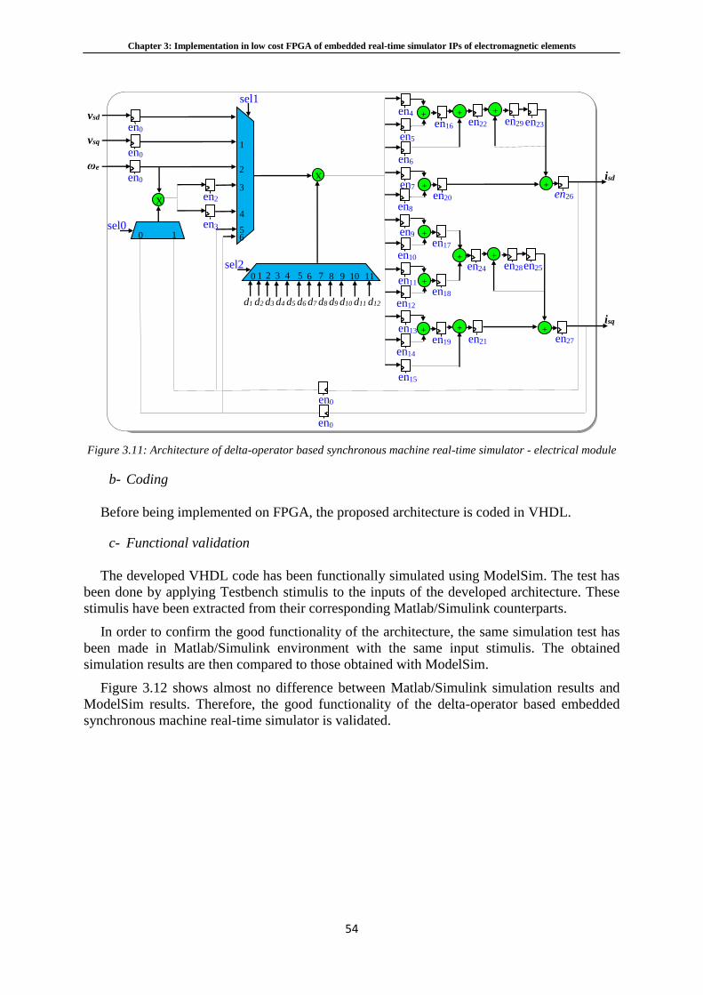
Chapter 3: Implementation in low cost FPGA of embedded real-time simulator IPs of electromagnetic elements
54
Figure 3.11: Architecture of delta-operator based synchronous machine real-time simulator - electrical module
b- Coding
Before being implemented on FPGA, the proposed architecture is coded in VHDL.
c- Functional validation
The developed VHDL code has been functionally simulated using ModelSim. The test has
been done by applying Testbench stimulis to the inputs of the developed architecture. These
stimulis have been extracted from their corresponding Matlab/Simulink counterparts.
In order to confirm the good functionality of the architecture, the same simulation test has
been made in Matlab/Simulink environment with the same input stimulis. The obtained
simulation results are then compared to those obtained with ModelSim.
Figure 3.12 shows almost no difference between Matlab/Simulink simulation results and
ModelSim results. Therefore, the good functionality of the delta-operator based embedded
synchronous machine real-time simulator is validated.
en0
en0
en0
X en2
en3
X
en4
en5
en6
en7
en8
en9
en10
en11
en12
en13
en14
en15
+
+
+
+
+
en0
en16
en20
en17
en18
en19
+
+
+
en22 +
en29 en23
+ en26
en24 +
en28 en25
+ en27
en0
d1 d2 d3 d4 d5 d6 d7 d8 d9 d10 d11 d12
en21
vsd
vsq
ωe isd
isq
1
2
3
4
5 6
0 1 2 3 4 5 6 7 8 9 10 11
0
0
1
sel1
sel2
1
sel0
1
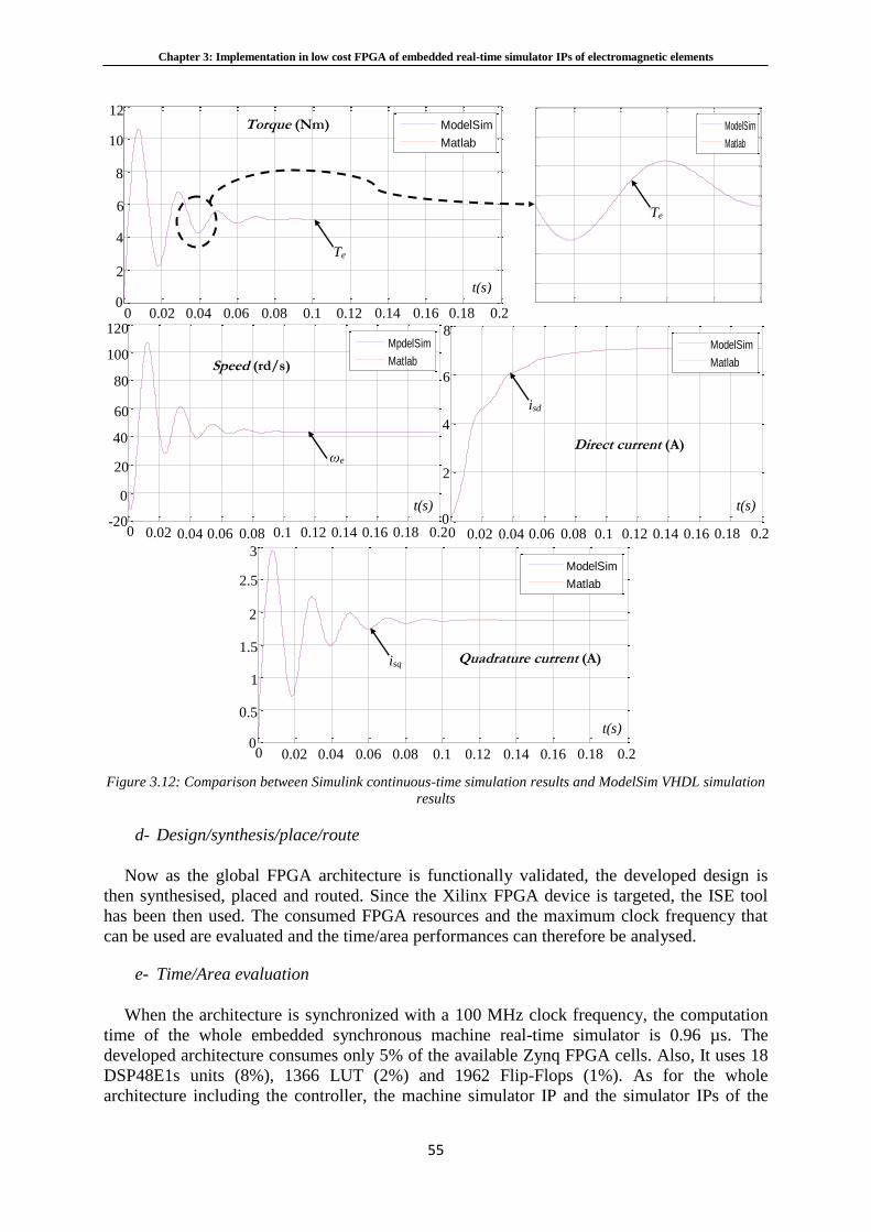
Chapter 3: Implementation in low cost FPGA of embedded real-time simulator IPs of electromagnetic elements
55
Figure 3.12: Comparison between Simulink continuous-time simulation results and ModelSim VHDL simulation
results
d- Design/synthesis/place/route
Now as the global FPGA architecture is functionally validated, the developed design is
then synthesised, placed and routed. Since the Xilinx FPGA device is targeted, the ISE tool
has been then used. The consumed FPGA resources and the maximum clock frequency that
can be used are evaluated and the time/area performances can therefore be analysed.
e- Time/Area evaluation
When the architecture is synchronized with a 100 MHz clock frequency, the computation
time of the whole embedded synchronous machine real-time simulator is 0.96 µs. The
developed architecture consumes only 5% of the available Zynq FPGA cells. Also, It uses 18
DSP48E1s units (8%), 1366 LUT (2%) and 1962 Flip-Flops (1%). As for the whole
architecture including the controller, the machine simulator IP and the simulator IPs of the
0 0.02 0.04 0.06 0.08 0.1 0.12 0.14 0.16 0.18 0.20
2
4
6
8
10
12
ModelSim
Matlab
0.04 0.045 0.05 0.055 0.06
3.5
4
4.5
5
5.5
6
6.5
ModelSim
Matlab
0 0.02 0.04 0.06 0.08 0.1 0.12 0.14 0.16 0.18 0.2-20
0
20
40
60
80
100
120
MpdelSim
Matlab
0 0.02 0.04 0.06 0.08 0.1 0.12 0.14 0.16 0.18 0.20
0.5
1
1.5
2
2.5
3
ModelSim
Matlab
0.02 0.04 0.06 0.08 0.1 0.12 0.14 0.16 0.18 0 0.2
4
6
0
8
10
12
2
20
40
-20
60
80
0
120
100
4
6
0
8
2
0 0.02 0.04 0.06 0.08 0.1 0.12 0.14 0.16 0.18 0.20
2
4
6
8
ModelSim
Matlab
1
1.5
0
2
2.5
3
0.5
0.02 0.04 0.06 0.08 0.1 0.12 0.14 0.16 0.18 0 0.2 0.02 0.04 0.06 0.08 0.1 0.12 0.14 0.16 0.18 0 0.2
0.02 0.04 0.06 0.08 0.1 0.12 0.14 0.16 0.18 0 0.2
Te
ωe
isd
isq
t(s)
t(s) t(s)
t(s)
Torque (Nm)
Speed (rd/s)
Direct current (A)
Quadrature current (A)
Te
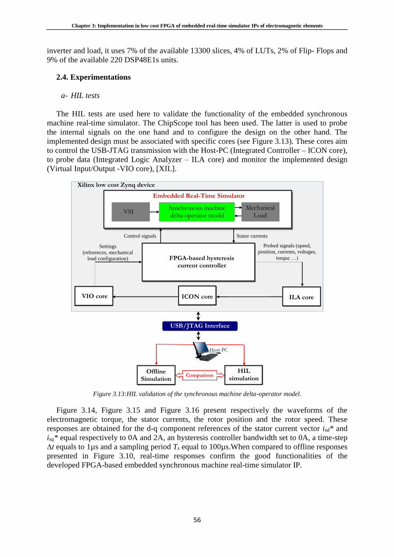
Chapter 3: Implementation in low cost FPGA of embedded real-time simulator IPs of electromagnetic elements
56
inverter and load, it uses 7% of the available 13300 slices, 4% of LUTs, 2% of Flip- Flops and
9% of the available 220 DSP48E1s units.
2.4. Experimentations
a- HIL tests
The HIL tests are used here to validate the functionality of the embedded synchronous
machine real-time simulator. The ChipScope tool has been used. The latter is used to probe
the internal signals on the one hand and to configure the design on the other hand. The
implemented design must be associated with specific cores (see Figure 3.13). These cores aim
to control the USB-JTAG transmission with the Host-PC (Integrated Controller – ICON core),
to probe data (Integrated Logic Analyzer – ILA core) and monitor the implemented design
(Virtual Input/Output -VIO core), [XIL].
Figure 3.13:HIL validation of the synchronous machine delta-operator model.
Figure 3.14, Figure 3.15 and Figure 3.16 present respectively the waveforms of the
electromagnetic torque, the stator currents, the rotor position and the rotor speed. These
responses are obtained for the d-q component references of the stator current vector isd* and
isq* equal respectively to 0A and 2A, an hysteresis controller bandwidth set to 0A, a time-step
∆t equals to 1µs and a sampling period Ts equal to 100µs.When compared to offline responses
presented in Figure 3.10, real-time responses confirm the good functionalities of the
developed FPGA-based embedded synchronous machine real-time simulator IP.
Embedded Real-Time Simulator
Synchronous machine delta-operator model
Mechanical Load
VSI
FPGA-based hysteresis current controller
Xilinx low cost Zynq device
Control signals Stator currents
Settings
(references, mechanical load configuration)
Probed signals (speed,
position, currents, voltages,
torque …)
ILA core ICON core VIO core
USB/JTAG Interface
Comparison HIL
simulation Offline
Simulation
Host-PC
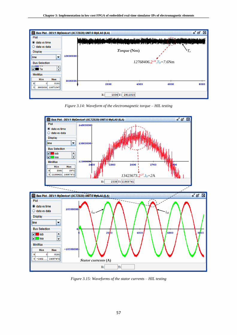
Chapter 3: Implementation in low cost FPGA of embedded real-time simulator IPs of electromagnetic elements
57
Figure 3.14: Waveform of the electromagnetic torque – HIL testing
Figure 3.15: Waveforms of the stator currents – HIL testing
isa isb
13423673.2-27.IB=2A
Stator currents (A)
12768406.2-24.TB=7.6Nm
Te Torque (Nm)
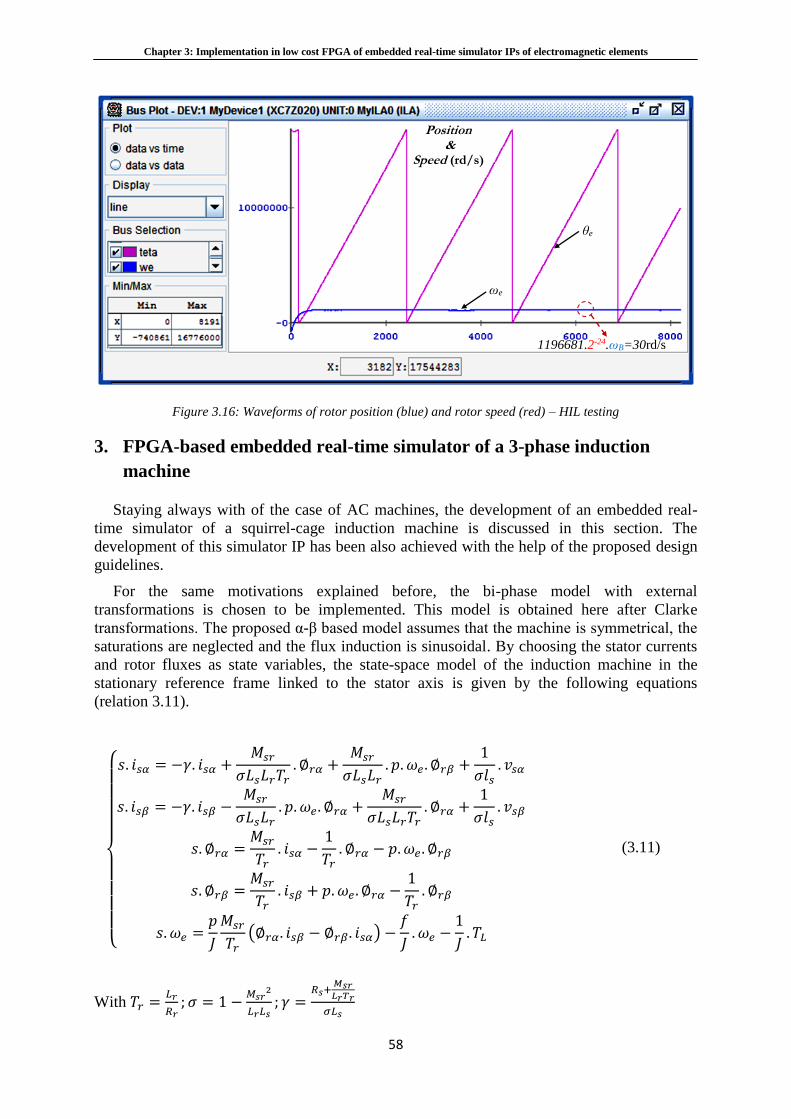
Chapter 3: Implementation in low cost FPGA of embedded real-time simulator IPs of electromagnetic elements
58
Figure 3.16: Waveforms of rotor position (blue) and rotor speed (red) – HIL testing
3. FPGA-based embedded real-time simulator of a 3-phase induction
machine
Staying always with of the case of AC machines, the development of an embedded real-
time simulator of a squirrel-cage induction machine is discussed in this section. The
development of this simulator IP has been also achieved with the help of the proposed design
guidelines.
For the same motivations explained before, the bi-phase model with external
transformations is chosen to be implemented. This model is obtained here after Clarke
transformations. The proposed α-β based model assumes that the machine is symmetrical, the
saturations are neglected and the flux induction is sinusoidal. By choosing the stator currents
and rotor fluxes as state variables, the state-space model of the induction machine in the
stationary reference frame linked to the stator axis is given by the following equations
(relation 3.11).
𝑠. 𝑖𝑠𝛼 = −𝛾. 𝑖𝑠𝛼 +
𝑀𝑠𝑟
𝜎𝐿𝑠𝐿𝑟𝑇𝑟. ∅𝑟𝛼 +
𝑀𝑠𝑟
𝜎𝐿𝑠𝐿𝑟. 𝑝. 𝜔𝑒 . ∅𝑟𝛽 +
1
𝜎𝑙𝑠. 𝑣𝑠𝛼
𝑠. 𝑖𝑠𝛽 = −𝛾. 𝑖𝑠𝛽 −𝑀𝑠𝑟
𝜎𝐿𝑠𝐿𝑟. 𝑝. 𝜔𝑒 . ∅𝑟𝛼 +
𝑀𝑠𝑟
𝜎𝐿𝑠𝐿𝑟𝑇𝑟. ∅𝑟𝛼 +
1
𝜎𝑙𝑠. 𝑣𝑠𝛽
𝑠. ∅𝑟𝛼 =𝑀𝑠𝑟
𝑇𝑟. 𝑖𝑠𝛼 −
1
𝑇𝑟. ∅𝑟𝛼 − 𝑝.𝜔𝑒 . ∅𝑟𝛽
𝑠. ∅𝑟𝛽 =𝑀𝑠𝑟
𝑇𝑟. 𝑖𝑠𝛽 + 𝑝.𝜔𝑒 . ∅𝑟𝛼 −
1
𝑇𝑟. ∅𝑟𝛽
𝑠. 𝜔𝑒 =𝑝
𝐽
𝑀𝑠𝑟
𝑇𝑟(∅𝑟𝛼. 𝑖𝑠𝛽 − ∅𝑟𝛽. 𝑖𝑠𝛼) −
𝑓
𝐽. 𝜔𝑒 −
1
𝐽. 𝑇𝐿
(3.11)
With 𝑇𝑟 =𝐿𝑟
𝑅𝑟; 𝜎 = 1 −
𝑀𝑠𝑟2
𝐿𝑟𝐿𝑠; 𝛾 =
𝑅𝑠+𝑀𝑠𝑟𝐿𝑟𝑇𝑟
𝜎𝐿𝑠
ωe
θe
Position &
Speed (rd/s)
1196681.2-24.ωB=30rd/s
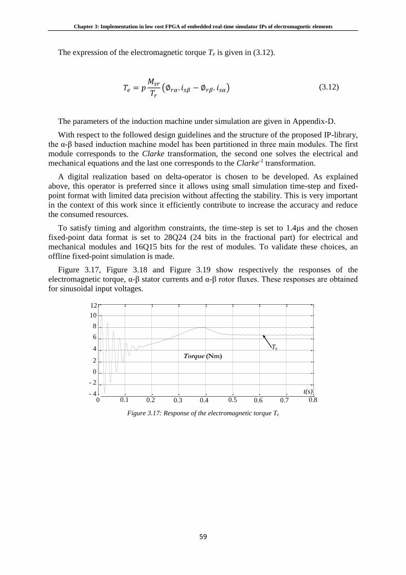
Chapter 3: Implementation in low cost FPGA of embedded real-time simulator IPs of electromagnetic elements
59
The expression of the electromagnetic torque Te is given in (3.12).
𝑇𝑒 = 𝑝𝑀𝑠𝑟
𝑇𝑟(∅𝑟𝛼. 𝑖𝑠𝛽 − ∅𝑟𝛽 . 𝑖𝑠𝛼) (3.12)
The parameters of the induction machine under simulation are given in Appendix-D.
With respect to the followed design guidelines and the structure of the proposed IP-library,
the α-β based induction machine model has been partitioned in three main modules. The first
module corresponds to the Clarke transformation, the second one solves the electrical and
mechanical equations and the last one corresponds to the Clarke-1 transformation.
A digital realization based on delta-operator is chosen to be developed. As explained
above, this operator is preferred since it allows using small simulation time-step and fixed-
point format with limited data precision without affecting the stability. This is very important
in the context of this work since it efficiently contribute to increase the accuracy and reduce
the consumed resources.
To satisfy timing and algorithm constraints, the time-step is set to 1.4µs and the chosen
fixed-point data format is set to 28Q24 (24 bits in the fractional part) for electrical and
mechanical modules and 16Q15 bits for the rest of modules. To validate these choices, an
offline fixed-point simulation is made.
Figure 3.17, Figure 3.18 and Figure 3.19 show respectively the responses of the
electromagnetic torque, α-β stator currents and α-β rotor fluxes. These responses are obtained
for sinusoidal input voltages.
Figure 3.17: Response of the electromagnetic torque Te
0 0.1 0.2 0.3 0.4 0.5 0.6 0.7 0.8-4
-2
0
2
4
6
8
10
12
0 0.1 0.2 0.3 0.4 0.5 - 4
0.6 0.7 0.8
- 2
0
2
4
6
8
10
12
Te
t(s)
Torque (Nm)
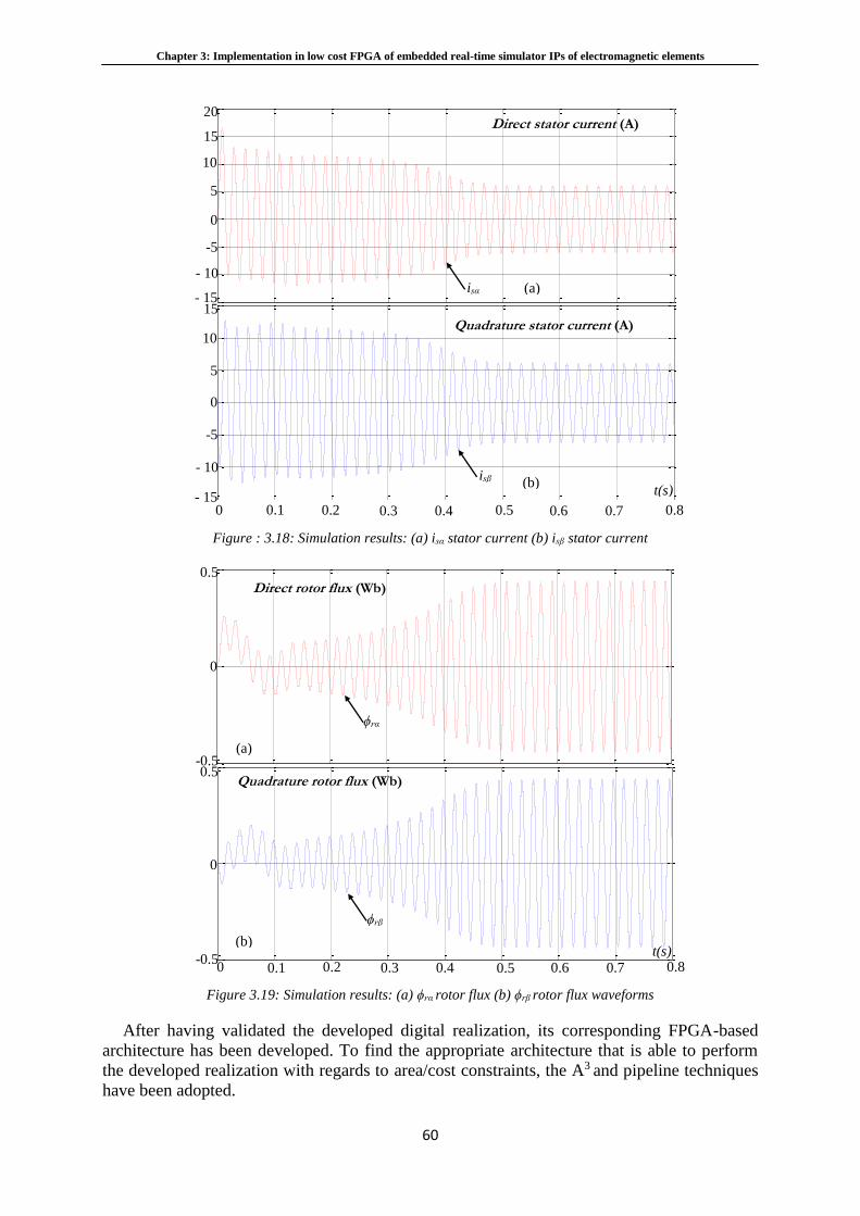
Chapter 3: Implementation in low cost FPGA of embedded real-time simulator IPs of electromagnetic elements
60
Figure : 3.18: Simulation results: (a) isα stator current (b) isβ stator current
Figure 3.19: Simulation results: (a) ϕrα rotor flux (b) ϕrβ rotor flux waveforms
After having validated the developed digital realization, its corresponding FPGA-based
architecture has been developed. To find the appropriate architecture that is able to perform
the developed realization with regards to area/cost constraints, the A3 and pipeline techniques
have been adopted.
0 0.1 0.2 0.3 0.4 0.5 0.6 0.7 0.8-0.5
0
0.5
0 0.1 0.2 0.3 0.4 0.5 0.6 0.7 0.8-0.5
0
0.5
0 0.1 0.2 0.3 0.4 0.5 0.6 0.7 0.8
-0.5
0
0.5
-0.5
0
0.5
(a)
(b)
ϕrα
ϕrβ
t(s)
Quadrature rotor flux (Wb)
Direct rotor flux (Wb)
0 0.1 0.2 0.3 0.4 0.5 0.6 0.7 0.8-15
-10
-5
0
5
10
15
20
0 0.1 0.2 0.3 0.4 0.5 - 15
0.6 0.7 0.8 0 0.1 0.2 0.3 0.4 0.5 0.6 0.7 0.8-15
-10
-5
0
5
10
15
- 10
-5
0
5
10
15 - 15
- 10
-5
0
5
10
15
20
(a)
(b)
isα
isβ t(s)
Quadrature stator current (A)
Direct stator current (A)
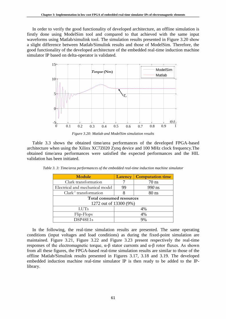
Chapter 3: Implementation in low cost FPGA of embedded real-time simulator IPs of electromagnetic elements
61
In order to verify the good functionality of developed architecture, an offline simulation is
firstly done using ModelSim tool and compared to that achieved with the same input
waveforms using Matlab/simulink tool. The simulation results presented in Figure 3.20 show
a slight difference between Matlab/Simulink results and those of ModelSim. Therefore, the
good functionality of the developed architecture of the embedded real-time induction machine
simulator IP based on delta-operator is validated.
Figure 3.20: Matlab and ModelSim simulation results
Table 3.3 shows the obtained time/area performances of the developed FPGA-based
architecture when using the Xilinx XC7Z020 Zynq device and 100 MHz clock frequency.The
obtained time/area performances were satisfied the expected performances and the HIL
validation has been initiated.
Table 3. 3: Time/area performances of the embedded real-time induction machine simulator
Module Latency Computation time
Clark transformation 7 70 ns
Electrical and mechanical model 99 990 ns
Clark-1 transformation 8 80 ns
Total consumed resources
1272 out of 13300 (9%)
LUTs 4%
Flip-Flops 4%
DSP48E1s 9%
In the following, the real-time simulation results are presented. The same operating
conditions (input voltages and load conditions) as during the fixed-point simulation are
maintained. Figure 3.21, Figure 3.22 and Figure 3.23 present respectively the real-time
responses of the electromagnetic torque, α-β stator currents and α-β rotor fluxes. As shown
from all these figures, the FPGA-based real-time simulation results are similar to those of the
offline Matlab/Simulink results presented in Figures 3.17, 3.18 and 3.19. The developed
embedded induction machine real-time simulator IP is then ready to be added to the IP-
library.
0 0.1 0.2 0.3 0.4 0.5 0.6 0.7 0.8 0.9 1-5
0
5
10
15
ModelSim
Matlab
0 0.1 0.2 0.3 0.4 0.5 0.6 0.7 0.8 0.9 1 -5
0
5
10
15
Te
t(s)
Torque (Nm)
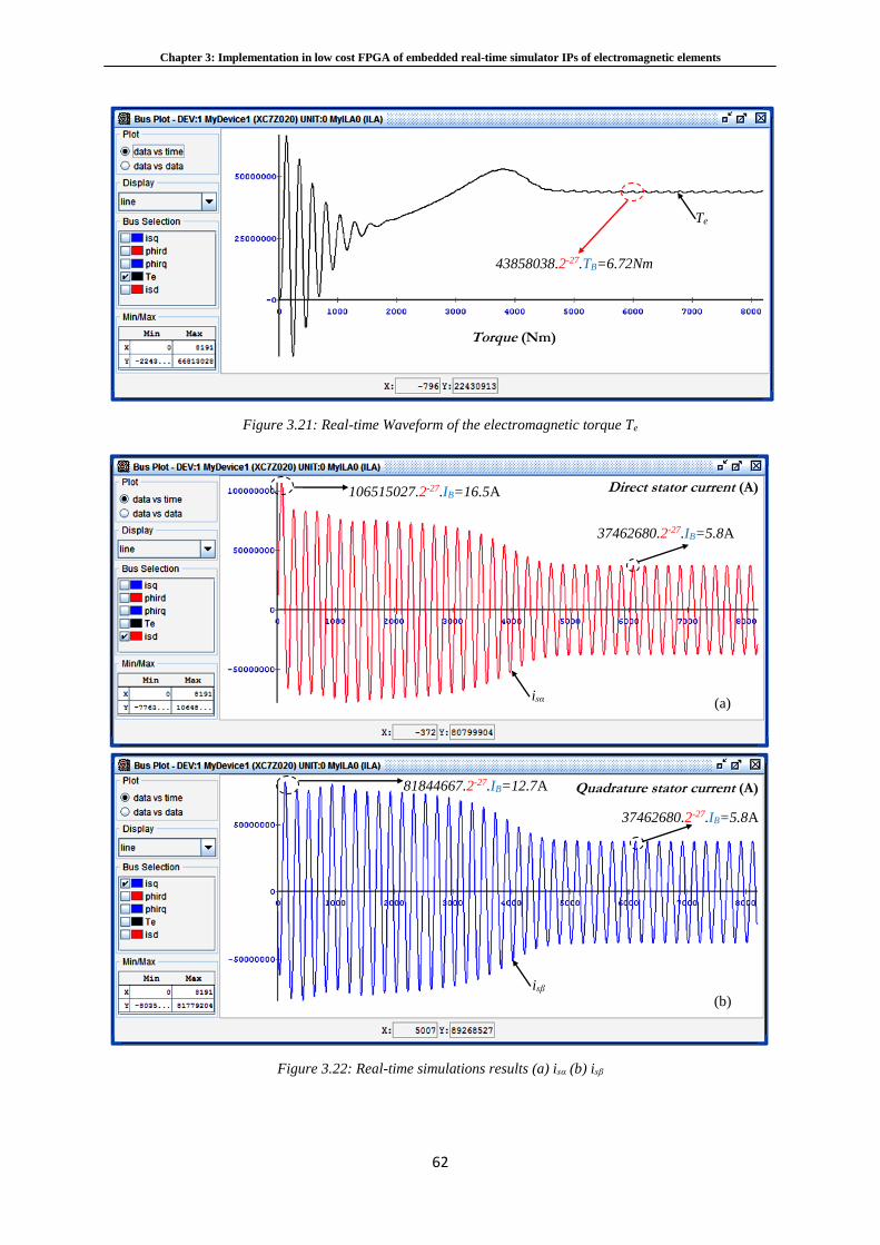
Chapter 3: Implementation in low cost FPGA of embedded real-time simulator IPs of electromagnetic elements
62
Figure 3.21: Real-time Waveform of the electromagnetic torque Te
Figure 3.22: Real-time simulations results (a) isα (b) isβ
(a)
(b)
isα
isβ
Direct stator current (A)
Quadrature stator current (A)
106515027.2-27.IB=16.5A
37462680.2-27.IB=5.8A
81844667.2-27.IB=12.7A
37462680.2-27.IB=5.8A
43858038.2-27.TB=6.72Nm
Te
Torque (Nm)
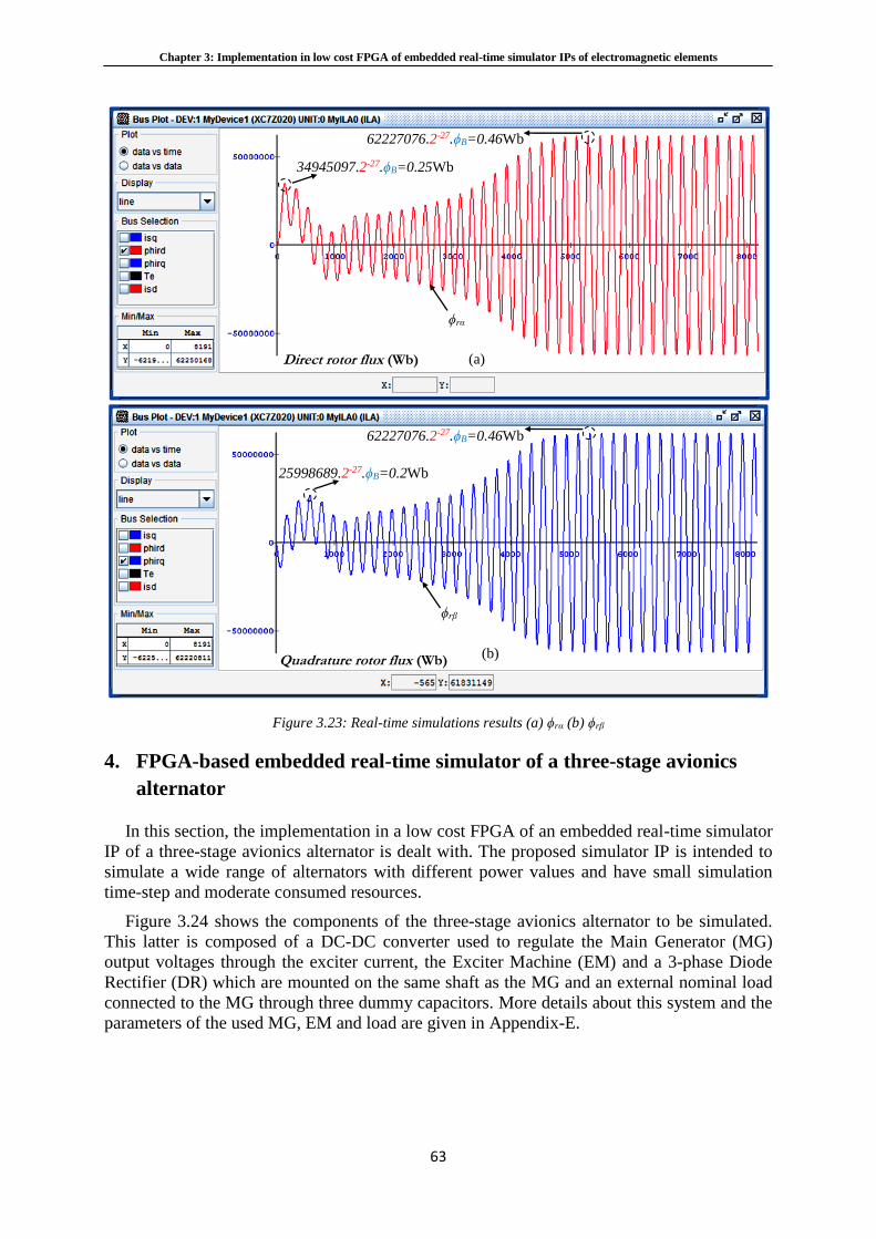
Chapter 3: Implementation in low cost FPGA of embedded real-time simulator IPs of electromagnetic elements
63
Figure 3.23: Real-time simulations results (a) ϕrα (b) ϕrβ
4. FPGA-based embedded real-time simulator of a three-stage avionics
alternator
In this section, the implementation in a low cost FPGA of an embedded real-time simulator
IP of a three-stage avionics alternator is dealt with. The proposed simulator IP is intended to
simulate a wide range of alternators with different power values and have small simulation
time-step and moderate consumed resources.
Figure 3.24 shows the components of the three-stage avionics alternator to be simulated.
This latter is composed of a DC-DC converter used to regulate the Main Generator (MG)
output voltages through the exciter current, the Exciter Machine (EM) and a 3-phase Diode
Rectifier (DR) which are mounted on the same shaft as the MG and an external nominal load
connected to the MG through three dummy capacitors. More details about this system and the
parameters of the used MG, EM and load are given in Appendix-E.
(a)
(b)
ϕrα
ϕrβ
Direct rotor flux (Wb)
Quadrature rotor flux (Wb)
34945097.2-27.ϕB=0.25Wb
62227076.2-27.ϕB=0.46Wb
25998689.2-27.ϕB=0.2Wb
62227076.2-27.ϕB=0.46Wb
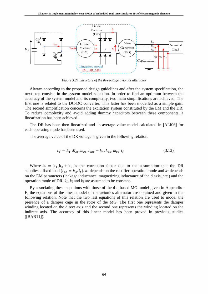
Chapter 3: Implementation in low cost FPGA of embedded real-time simulator IPs of electromagnetic elements
64
Figure 3.24: Structure of the three-stage avionics alternator
Always according to the proposed design guidelines and after the system specification, the
next step consists in the system model selection. In order to find an optimum between the
accuracy of the system model and its complexity, two main simplifications are achieved. The
first one is related to the DC-DC converter. This latter has been modelled as a simple gain.
The second simplification concerns the excitation system constituted by the EM and the DR.
To reduce complexity and avoid adding dummy capacitors between these components, a
linearization has been achieved.
The DR has been then linearized and its average-value model calculated in [ALI06] for
each operating mode has been used.
The average value of the DR voltage is given in the following relation.
𝑣𝑓 = 𝑘1. 𝑀𝑠𝑒 . 𝜔𝑒𝑒 . 𝑖𝑒𝑥𝑐 − 𝑘4. 𝐿𝑑𝑒 . 𝜔𝑒𝑒. 𝑖𝑓 (3.13)
Where k4 = k1. k3 + k2 is the correction factor due to the assumption that the DR
supplies a fixed load (𝑖𝑑𝑒 = 𝑘3. 𝑖𝑓). k1 depends on the rectifier operation mode and k2 depends
on the EM parameters (leakage inductance, magnetizing inductance of the d axis, etc.) and the
operation mode of DR. k1, k2 and k3 are assumed to be constant.
By associating these equations with those of the d-q based MG model given in Appendix-
E, the equations of the linear model of the avionics alternator are obtained and given in the
following relation. Note that the two last equations of this relation are used to model the
presence of a damper cage in the rotor of the MG. The first one represents the damper
winding located on the direct axis and the second one represents the winding located on the
indirect axis. The accuracy of this linear model has been proved in previous studies
([BAR11]).
vf
Exciter Machine
(EM)
C
C
vexc iexc Main
Generator
(MG)
Cap
if Diode
Rectifier (DR)
Vdc
iap Nominal
Load
ibp icp
vap vbp vcp
Linearized model EM_DR_MG
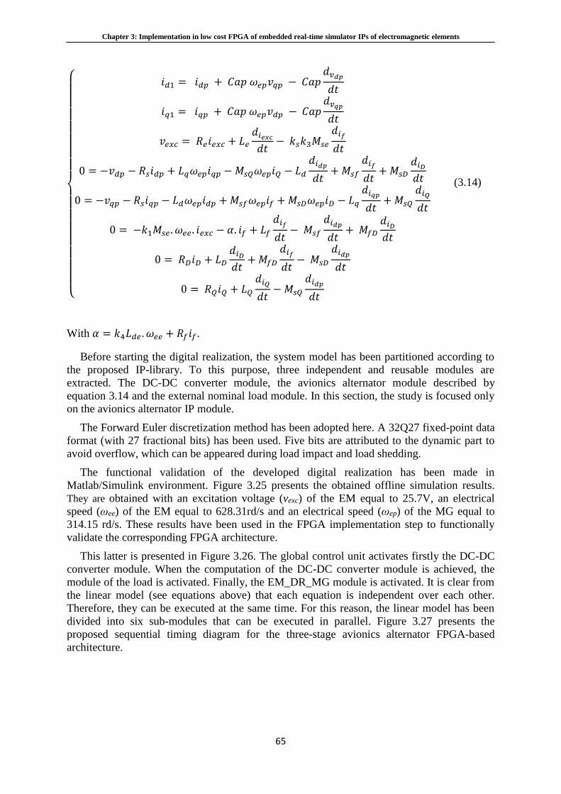
Chapter 3: Implementation in low cost FPGA of embedded real-time simulator IPs of electromagnetic elements
65
𝑖𝑑1 = 𝑖𝑑𝑝 + 𝐶𝑎𝑝 𝜔𝑒𝑝𝑣𝑞𝑝 − 𝐶𝑎𝑝
𝑑𝑣𝑑𝑝𝑑𝑡
𝑖𝑞1 = 𝑖𝑞𝑝 + 𝐶𝑎𝑝 𝜔𝑒𝑝𝑣𝑑𝑝 − 𝐶𝑎𝑝𝑑𝑣𝑞𝑝𝑑𝑡
𝑣𝑒𝑥𝑐 = 𝑅𝑒𝑖𝑒𝑥𝑐 + 𝐿𝑒𝑑𝑖𝑒𝑥𝑐𝑑𝑡
− 𝑘𝑠𝑘3𝑀𝑠𝑒
𝑑𝑖𝑓𝑑𝑡
0 = −𝑣𝑑𝑝 − 𝑅𝑠𝑖𝑑𝑝 + 𝐿𝑞𝜔𝑒𝑝𝑖𝑞𝑝 −𝑀𝑠𝑄𝜔𝑒𝑝𝑖𝑄 − 𝐿𝑑𝑑𝑖𝑑𝑝𝑑𝑡
+ 𝑀𝑠𝑓
𝑑𝑖𝑓𝑑𝑡+ 𝑀𝑠𝐷
𝑑𝑖𝐷𝑑𝑡
0 = −𝑣𝑞𝑝 − 𝑅𝑠𝑖𝑞𝑝 − 𝐿𝑑𝜔𝑒𝑝𝑖𝑑𝑝 +𝑀𝑠𝑓𝜔𝑒𝑝𝑖𝑓 +𝑀𝑠𝐷𝜔𝑒𝑝𝑖𝐷 − 𝐿𝑞𝑑𝑖𝑞𝑝𝑑𝑡
+ 𝑀𝑠𝑄
𝑑𝑖𝑄𝑑𝑡
0 = −𝑘1𝑀𝑠𝑒 . 𝜔𝑒𝑒. 𝑖𝑒𝑥𝑐 − 𝛼. 𝑖𝑓 + 𝐿𝑓𝑑𝑖𝑓𝑑𝑡− 𝑀𝑠𝑓
𝑑𝑖𝑑𝑝𝑑𝑡
+ 𝑀𝑓𝐷𝑑𝑖𝐷𝑑𝑡
0 = 𝑅𝐷𝑖𝐷 + 𝐿𝐷𝑑𝑖𝐷𝑑𝑡
+ 𝑀𝑓𝐷𝑑𝑖𝑓
𝑑𝑡− 𝑀𝑠𝐷
𝑑𝑖𝑑𝑝𝑑𝑡
0 = 𝑅𝑄𝑖𝑄 + 𝐿𝑄𝑑𝑖𝑄𝑑𝑡
− 𝑀𝑠𝑄
𝑑𝑖𝑑𝑝𝑑𝑡
(3.14)
With 𝛼 = 𝑘4𝐿𝑑𝑒 . 𝜔𝑒𝑒 + 𝑅𝑓𝑖𝑓.
Before starting the digital realization, the system model has been partitioned according to
the proposed IP-library. To this purpose, three independent and reusable modules are
extracted. The DC-DC converter module, the avionics alternator module described by
equation 3.14 and the external nominal load module. In this section, the study is focused only
on the avionics alternator IP module.
The Forward Euler discretization method has been adopted here. A 32Q27 fixed-point data
format (with 27 fractional bits) has been used. Five bits are attributed to the dynamic part to
avoid overflow, which can be appeared during load impact and load shedding.
The functional validation of the developed digital realization has been made in
Matlab/Simulink environment. Figure 3.25 presents the obtained offline simulation results.
They are obtained with an excitation voltage (vexc) of the EM equal to 25.7V, an electrical
speed (ωee) of the EM equal to 628.31rd/s and an electrical speed (ωep) of the MG equal to
314.15 rd/s. These results have been used in the FPGA implementation step to functionally
validate the corresponding FPGA architecture.
This latter is presented in Figure 3.26. The global control unit activates firstly the DC-DC
converter module. When the computation of the DC-DC converter module is achieved, the
module of the load is activated. Finally, the EM_DR_MG module is activated. It is clear from
the linear model (see equations above) that each equation is independent over each other.
Therefore, they can be executed at the same time. For this reason, the linear model has been
divided into six sub-modules that can be executed in parallel. Figure 3.27 presents the
proposed sequential timing diagram for the three-stage avionics alternator FPGA-based
architecture.
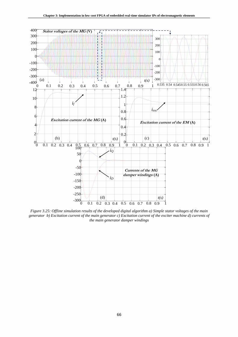
Chapter 3: Implementation in low cost FPGA of embedded real-time simulator IPs of electromagnetic elements
66
Figure 3.25: Offline simulation results of the developed digital algorithm a) Simple stator voltages of the main
generator b) Excitation current of the main generator c) Excitation current of the exciter machine d) currents of
the main generator damper windings
0 0.1 0.2 0.3 0.4 0.5 0.6 0.7 0.8 0.9 1-400
-300
-200
-100
0
100
200
300
400
0 0.1 0.2 0.3 0.4 0.5 0.6 0.7 0.8 0.9 10
2
4
6
8
10
12
0 0.1 0.2 0.3 0.4 0.5 0.6 0.7 0.8 0.9 1-300
-250
-200
-150
-100
-50
0
50
100
0 0.1 0.2 0.3 0.4 0.5 0.6 0.7 0.8 0.9 1 -400
-200
0
100
200
300
400
-100
-300 -200
0
100
200
300
-100
-300
0.535 0.54 0.545 0.55 0.555 0.56 0.565
-300
-200
-100
0
100
200
300
0.535 0.54 0.545 0.55 0.555 0.56
0 0.1 0.2 0.3 0.4 0.5 0.6 0.7 0.8 0.9 1 0 0.1 0.2 0.3 0.4 0.5 0.6 0.7 0.8 0.9
0 0.1 0.2 0.3 0.4 0.5 0.6 0.7 0.8 0.9 1
0
6
8
10
12
4
2
0
0.6
0.8
1
1.2
0.4
0.2
0 0.1 0.2 0.3 0.4 0.5 0.6 0.7 0.8 0.9 10
0.2
0.4
0.6
0.8
1
1.2
1.4
1
1.4
-300
-200
0
-100
-50
-150
-250
100
50
if
iexc
iD
iQ
(a)
t(s) (c)
(d)
0.565
(b) t(s)
t(s)
t(s)
Stator voltages of the MG (V)
Excitation current of the MG (A) Excitation current of the EM (A)
Currents of the MG damper windings (A)
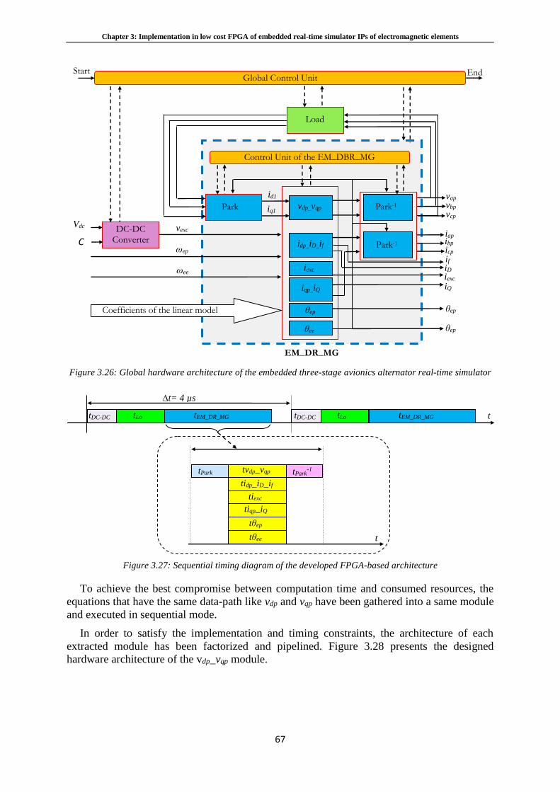
Chapter 3: Implementation in low cost FPGA of embedded real-time simulator IPs of electromagnetic elements
67
Figure 3.26: Global hardware architecture of the embedded three-stage avionics alternator real-time simulator
Figure 3.27: Sequential timing diagram of the developed FPGA-based architecture
To achieve the best compromise between computation time and consumed resources, the
equations that have the same data-path like vdp and vqp have been gathered into a same module
and executed in sequential mode.
In order to satisfy the implementation and timing constraints, the architecture of each
extracted module has been factorized and pipelined. Figure 3.28 presents the designed
hardware architecture of the vdp_vqp module.
t tDC-DC
∆t= 4 µs
tLo tEM_DR_MG
tDC-DC tLo tEM_DR_MG
tPark
tPark
-1
tvdp_vqp
tidp_iD_if
tiexc
tiqp_iQ
tθep
tθee
t
Park vap
iap
θep
θep
ωep
vexc
Control Unit of the EM_DBR_MG
ωee
if
Park-1 vdp_vqp
idp_iD_if
iexc
iqp_iQ
θep
θee
id1
iq1
Load
DC-DC Converter
Global Control Unit
Coefficients of the linear model
Vdc
EM_DR_MG
PD3_GP
C
Start End
Park-1
vbp vcp
ibp icp
iD iexc iQ
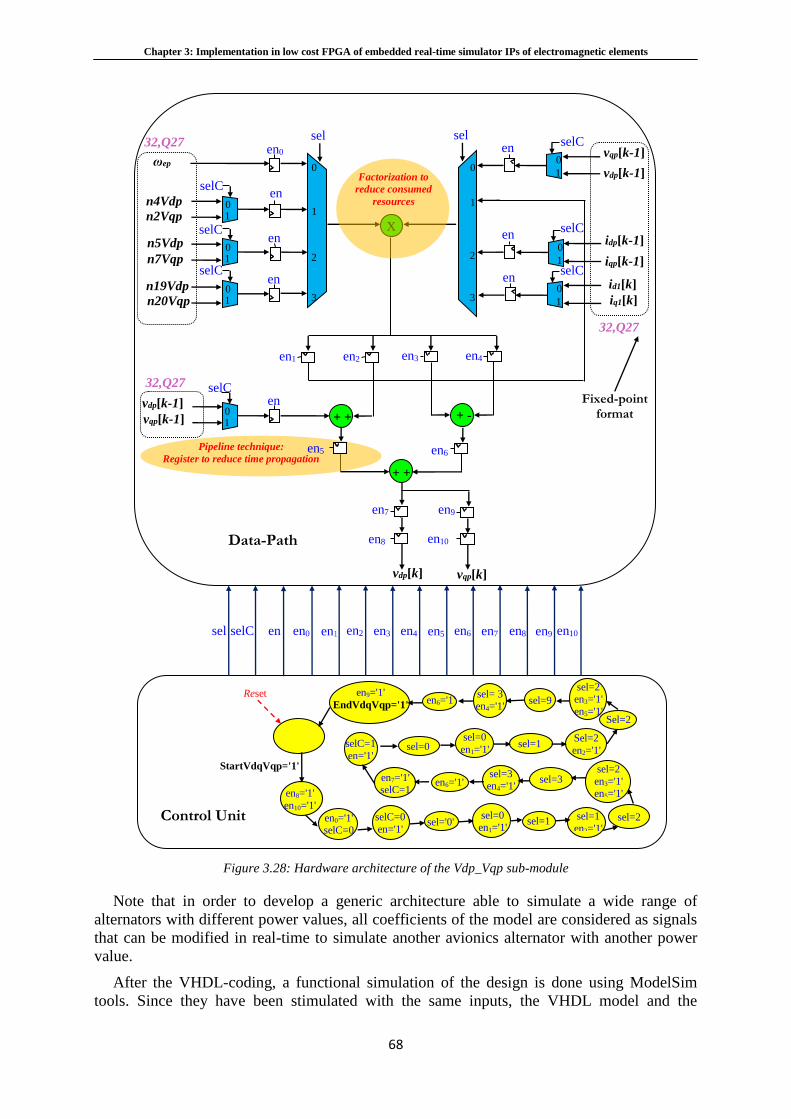
Chapter 3: Implementation in low cost FPGA of embedded real-time simulator IPs of electromagnetic elements
68
Figure 3.28: Hardware architecture of the Vdp_Vqp sub-module
Note that in order to develop a generic architecture able to simulate a wide range of
alternators with different power values, all coefficients of the model are considered as signals
that can be modified in real-time to simulate another avionics alternator with another power
value.
After the VHDL-coding, a functional simulation of the design is done using ModelSim
tools. Since they have been stimulated with the same inputs, the VHDL model and the
X
en0
+ +
vdp[k] vqp[k]
ωep
n4Vdp
n2Vqp
n5Vdp
n7Vqp
n19Vdp
n20Vqp
vdp[k-1]
vdp[k-1]
vqp[k-1]
vqp[k-1]
idp[k-1]
id1[k]
iqp[k-1]
iq1[k]
selC
en9='1'
EndVdqVqp='1'
en6='1' sel= 3 en4='1'
sel=9
sel=2 en3='1'
en5='1'
E
EndVdqVqpp=1
Sel=2
Sel=2
en2='1'
sel=1
sel=0
en1='1'
sel=0
selC=1
en='1'
en7='1' selC=1
en6='1'
sel=3 en4='1'
sel=3
sel=2
en3='1' en5='1'
sel=2
sel=1
en2='1'
sel=1
sel=0 en1='1'
sel='0'
selC=0
en='1'
en0='1' selC=0
en8='1'
en10='1'
Reset
StartVdqVqp='1'
sel selC en
32,Q27
32,Q27
32,Q27
Fixed-point format
Data-Path
Control Unit
Factorization to
reduce consumed
resources
Pipeline technique:
Register to reduce time propagation
selC
sel selC
selC
selC
en
selC
en0 en1 en2 en3 en4 en5 en6 en7 en8 en9 en10
en1
+ -
+ +
en6 en5
en7
en8
en9
en10
0
1
2
3
0
1
2
3
sel
0 1
0
0 1
0
0 1
0
selC
0 1
0
0
1
0
0
1
0
0
1
0
en
en
en
en
en
en
en2 en3 en4
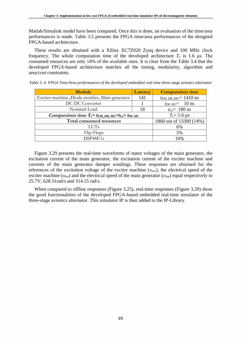
Chapter 3: Implementation in low cost FPGA of embedded real-time simulator IPs of electromagnetic elements
69
Matlab/Simulink model have been compared. Once this is done, an evaluation of the time/area
performances is made. Table 3.5 presents the FPGA time/area performances of the designed
FPGA-based architecture.
These results are obtained with a Xilinx XC7Z020 Zynq device and 100 MHz clock
frequency. The whole computation time of the developed architecture Tc is 1.6 μs. The
consumed resources are only 14% of the available ones. It is clear from the Table 3.4 that the
developed FPGA-based architecture matches all the timing, modularity, algorithm and
area/cost constraints.
Table 3. 4: FPGA Time/Area performances of the developed embedded real-time three-stage avionics alternator
Module Latency Computation time
Exciter-machine_Diode-rectifier_Main-generator 141 tEM_DR_MG= 1410 ns
DC-DC Converter 1 tDC-DC= 10 ns
Nominal Load 18 tLo= 180 ns
Computation time Tc= tEM_DR_MG+tLo+ tDC-DC Tc= 1.6 µs
Total consumed resources 1868 out of 13300 (14%)
LUTs 6%
Flip-Flops 5%
DSP48E1s 16%
Figure 3.29 presents the real-time waveforms of stator voltages of the main generator, the
excitation current of the main generator, the excitation current of the exciter machine and
currents of the main generator damper windings. These responses are obtained for the
references of the excitation voltage of the exciter machine (vexc), the electrical speed of the
exciter machine (ωee) and the electrical speed of the main generator (ωep) equal respectively to
25.7V, 628.31rad/s and 314.15 rad/s.
When compared to offline responses (Figure 3.25), real-time responses (Figure 3.29) show
the good functionalities of the developed FPGA-based embedded real-time simulator of the
three-stage avionics alternator. This simulator IP is then added to the IP-Library.
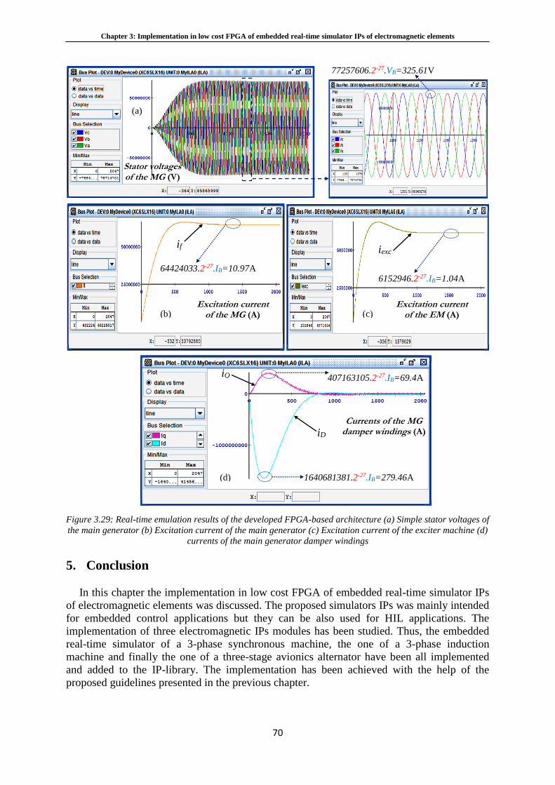
Chapter 3: Implementation in low cost FPGA of embedded real-time simulator IPs of electromagnetic elements
70
Figure 3.29: Real-time emulation results of the developed FPGA-based architecture (a) Simple stator voltages of
the main generator (b) Excitation current of the main generator (c) Excitation current of the exciter machine (d)
currents of the main generator damper windings
5. Conclusion
In this chapter the implementation in low cost FPGA of embedded real-time simulator IPs
of electromagnetic elements was discussed. The proposed simulators IPs was mainly intended
for embedded control applications but they can be also used for HIL applications. The
implementation of three electromagnetic IPs modules has been studied. Thus, the embedded
real-time simulator of a 3-phase synchronous machine, the one of a 3-phase induction
machine and finally the one of a three-stage avionics alternator have been all implemented
and added to the IP-library. The implementation has been achieved with the help of the
proposed guidelines presented in the previous chapter.
77257606.2-27.VB=325.61V
64424033.2-27.IB=10.97A 6152946.2-27.IB=1.04A
(a)
(b) (c)
(d)
iexc if
iD
iQ
Stator voltages of the MG (V)
Excitation current of the MG (A)
Excitation current of the EM (A)
Currents of the MG damper windings (A)
407163105.2-27.IB=69.4A
1640681381.2-27.IB=279.46A

Chapter 3: Implementation in low cost FPGA of embedded real-time simulator IPs of electromagnetic elements
71
The obtained results show the ability of all developed electromagnetic IPs to reproduce
accurately the dynamic behaviors of the simulated electromagnetic elements. They show also
that all developed simulator IPs enables the use of small simulation time-step and consumes
moderate hardware resources. Their ability to address both embedded control and HIL
applications was then confirmed.
In this chapter, the advantages of using delta operator rather than shift operator to design
digital realizations of AC machines were also examined. It has been shown that delta-operator
based realization is more convenient in the context of this work since it allows using small
simulation time-step and limited fixed-point data word length without affecting the system
stability.
In the next chapter the implementation in low cost FPGA of embedded real-time simulator
IPs of switching elements will be discussed.
Chapter 4: Implementation in low cost FPGA of embedded real-time simulator IPs of switching elements
72
Chapter 4
Implementation in low cost FPGA of embedded real-
time simulator IPs of switching elements
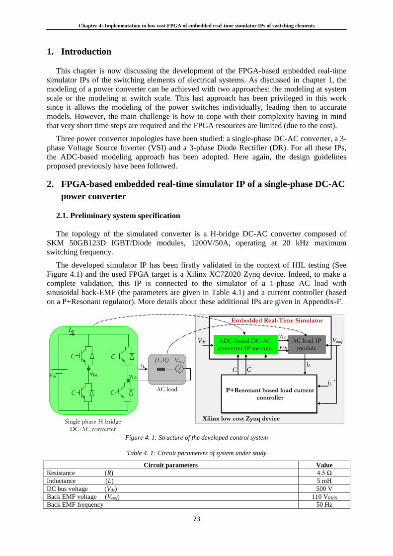
Chapter 4: Implementation in low cost FPGA of embedded real-time simulator IPs of switching elements
73
1. Introduction
This chapter is now discussing the development of the FPGA-based embedded real-time
simulator IPs of the switching elements of electrical systems. As discussed in chapter 1, the
modeling of a power converter can be achieved with two approaches: the modeling at system
scale or the modeling at switch scale. This last approach has been privileged in this work
since it allows the modeling of the power switches individually, leading then to accurate
models. However, the main challenge is how to cope with their complexity having in mind
that very short time steps are required and the FPGA resources are limited (due to the cost).
Three power converter topologies have been studied: a single-phase DC-AC converter, a 3-
phase Voltage Source Inverter (VSI) and a 3-phase Diode Rectifier (DR). For all these IPs,
the ADC-based modeling approach has been adopted. Here again, the design guidelines
proposed previously have been followed.
2. FPGA-based embedded real-time simulator IP of a single-phase DC-AC
power converter
2.1. Preliminary system specification
The topology of the simulated converter is a H-bridge DC-AC converter composed of
SKM 50GB123D IGBT/Diode modules, 1200V/50A, operating at 20 kHz maximum
switching frequency.
The developed simulator IP has been firstly validated in the context of HIL testing (See
Figure 4.1) and the used FPGA target is a Xilinx XC7Z020 Zynq device. Indeed, to make a
complete validation, this IP is connected to the simulator of a 1-phase AC load with
sinusoidal back-EMF (the parameters are given in Table 4.1) and a current controller (based
on a P+Resonant regulator). More details about these additional IPs are given in Appendix-F.
Figure 4. 1: Structure of the developed control system
Table 4. 1: Circuit parameters of system under study
Circuit parameters Value
Resistance (R) 4.5 Ω
Inductance (L) 5 mH
DC bus voltage (Vdc) 500 V
Back EMF voltage (Vemf) 110 VRMS
Back EMF frequency 50 Hz
Embedded Real-Time Simulator
ADC-based DC-AC converter IP module
AC load IP module
P+Resonant based load current controller
Xilinx low cost Zynq device
Vdc
(L,R) Vemf C
C
C
C
Single phase H-bridge DC-AC converter
AC load
vLa vLb
iL
vLa
vLb
iL C C
iL *
Vemf Vdc
Idc
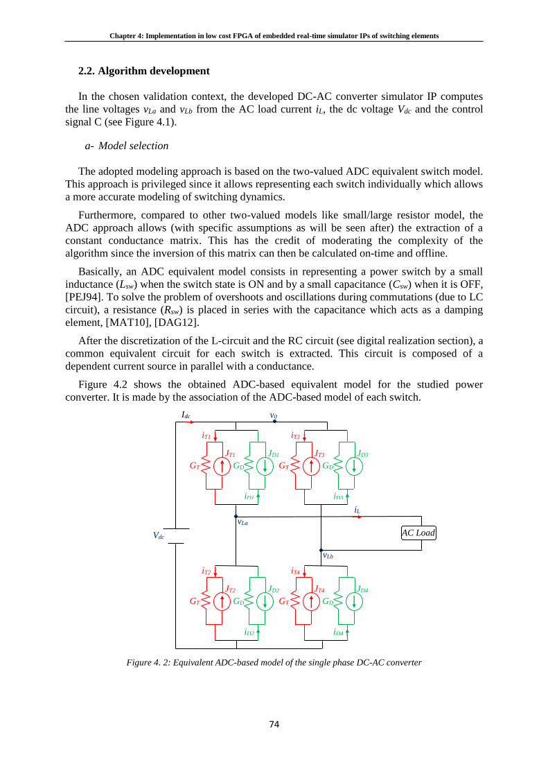
Chapter 4: Implementation in low cost FPGA of embedded real-time simulator IPs of switching elements
74
2.2. Algorithm development
In the chosen validation context, the developed DC-AC converter simulator IP computes
the line voltages vLa and vLb from the AC load current iL, the dc voltage Vdc and the control
signal C (see Figure 4.1).
a- Model selection
The adopted modeling approach is based on the two-valued ADC equivalent switch model.
This approach is privileged since it allows representing each switch individually which allows
a more accurate modeling of switching dynamics.
Furthermore, compared to other two-valued models like small/large resistor model, the
ADC approach allows (with specific assumptions as will be seen after) the extraction of a
constant conductance matrix. This has the credit of moderating the complexity of the
algorithm since the inversion of this matrix can then be calculated on-time and offline.
Basically, an ADC equivalent model consists in representing a power switch by a small
inductance (Lsw) when the switch state is ON and by a small capacitance (Csw) when it is OFF,
[PEJ94]. To solve the problem of overshoots and oscillations during commutations (due to LC
circuit), a resistance (Rsw) is placed in series with the capacitance which acts as a damping
element, [MAT10], [DAG12].
After the discretization of the L-circuit and the RC circuit (see digital realization section), a
common equivalent circuit for each switch is extracted. This circuit is composed of a
dependent current source in parallel with a conductance.
Figure 4.2 shows the obtained ADC-based equivalent model for the studied power
converter. It is made by the association of the ADC-based model of each switch.
Figure 4. 2: Equivalent ADC-based model of the single phase DC-AC converter
Idc
JD1
iD1
v0
JT1
iT1
vLa
vLb
iL
AC Load Vdc
GD GT
iD3
JT3
iT3
GD GT
JD2
iD2
JT2
iT2
GD GT
iD4
JT4
iT4
GD GT
JD3
JD4
Chapter 4: Implementation in low cost FPGA of embedded real-time simulator IPs of switching elements
75
In this equivalent circuit, JTi and JDi are respectively the dependent currents sources of the
ith controllable (IGBT) and uncontrollable (diode) switches. v0, vLa and vLb are the node
voltages. iTi and iDi are the branch currents. GT and GD are the equivalent conductances. As it
will be seen in the digital realization section, all these data are updated at each time-step ∆t
according to the switch state.
Then, the state of the IGBT is updated depending on the control signal, the voltage nodes
and the branch current as given in the following logic equation.
𝑠𝑇[𝑘] = 𝐶[𝑘]. (𝑖𝑇[𝑘 − 1] ≥ 0)
(4.1)
As for the diode, the state is updated as follows:
𝑠𝐷[𝑘] = 𝑠𝐷[𝑘 − 1]. (𝑖𝐷[𝑘 − 1] ≥ 0) + 𝑠𝐷[𝑘 − 1] . (𝑉𝐷[𝑘 − 1] ≥ 0)
(4.2)
Thus, when the switch is ON:
𝐽𝑇/𝐷[𝑘] = −𝑖𝑇/𝐷[𝑘 − 1]
𝐺𝑇/𝐷 =∆𝑡
𝐿𝑠𝑤𝑉𝑇/𝐷[𝑘] = 𝑓(𝑣0, 𝑣𝐿𝑎 , 𝑣𝐿𝑏)
𝑖𝑇/𝐷[𝑘] = 𝐺𝑇/𝐷 . 𝑣𝑇/𝐷[𝑘] + 𝑖𝑇/𝐷[𝑘 − 1]
(4.3)
and when it is OFF
𝐽𝑇/𝐷[𝑘] = 𝐺𝑇/𝐷 . 𝑉𝑇/𝐷[𝑘 − 1]
𝐺𝑇/𝐷 =𝐶𝑠𝑤
𝑅𝑠𝑤 . 𝐶𝑠𝑤 + ∆𝑡
𝑉𝑇/𝐷[𝑘] = 𝑓(𝑣0, 𝑣𝐿𝑎 , 𝑣𝐿𝑏)
𝑖𝑇/𝐷[𝑘] = 𝐺𝑇/𝐷 . 𝑣𝑇/𝐷[𝑘] − 𝐽𝑇/𝐷[𝑘]
(4.4)
To extract the relations between voltages and currents of the whole power converter, a
nodal analysis is made. The Modified Nodal Analysis (MNA), [PEJ94], can be applied to
extract these relations as a matrix equation:
𝐻. 𝑥[𝑘] = 𝑏[𝑘] (4.5)
Where, H is the conductance matrix. The vector x[k] gathers the node voltages v0[k] and
vLi(i=a,b)[k] and the dc-current Idc[k]. The vector b[k] is built from combinations, at each
voltage node, of JTi[k]/JDi[k] and iL[k]. It also includes the dc-voltage Vdc[k]. The system
solution is computed at each simulation time-step ∆t by solving the matrix equation (4.6).
𝑥[𝑘] = 𝐻−1 . 𝑏[𝑘] (4.6)
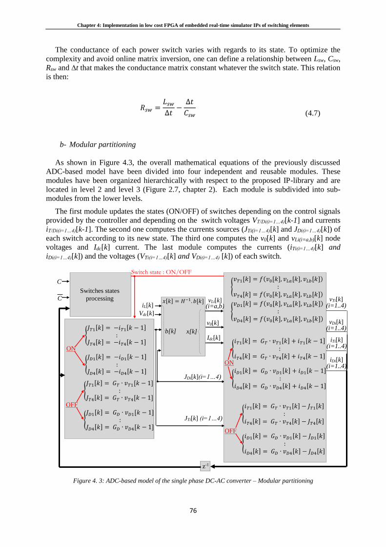
Chapter 4: Implementation in low cost FPGA of embedded real-time simulator IPs of switching elements
76
The conductance of each power switch varies with regards to its state. To optimize the
complexity and avoid online matrix inversion, one can define a relationship between Lsw, Csw,
Rsw and ∆t that makes the conductance matrix constant whatever the switch state. This relation
is then:
𝑅𝑠𝑤 =𝐿𝑠𝑤∆𝑡
−∆𝑡
𝐶𝑠𝑤
(4.7)
b- Modular partitioning
As shown in Figure 4.3, the overall mathematical equations of the previously discussed
ADC-based model have been divided into four independent and reusable modules. These
modules have been organized hierarchically with respect to the proposed IP-library and are
located in level 2 and level 3 (Figure 2.7, chapter 2). Each module is subdivided into sub-
modules from the lower levels.
The first module updates the states (ON/OFF) of switches depending on the control signals
provided by the controller and depending on the switch voltages VT/Di(i=1…4)[k-1] and currents
iT/Di(i=1…4)[k-1]. The second one computes the currents sources (JTi(i=1…4)[k] and JDi(i=1…4)[k]) of
each switch according to its new state. The third one computes the v0[k] and vLi(i=a,b)[k] node
voltages and Idc[k] current. The last module computes the currents (iTi(i=1…4)[k] and
iDi(i=1…4)[k]) and the voltages (VTi(i=1…4)[k] and VDi(i=1…4) [k]) of each switch.
Figure 4. 3: ADC-based model of the single phase DC-AC converter – Modular partitioning
𝑥[𝑘] = 𝐻−1. 𝑏[𝑘]
b[k] x[k]
JTi[k] (i=1…4)
JDi[k](i=1…4)
vLi[k] (i=a,b) iL[k]
Vdc[k]
Idc[k]
v0[k]
z-1
Switches states
processing
vDi[k] (i=1..4)
iTi[k] (i=1..4)
iDi[k] (i=1..4)
OFF
𝑖𝑇1[𝑘] = 𝐺𝑇 ∙ 𝑣𝑇1[𝑘] − 𝐽𝑇1[𝑘]
:𝑖𝑇4[𝑘] = 𝐺𝑇 ∙ 𝑣𝑇4[𝑘] − 𝐽𝑇4[𝑘]
𝑖𝐷1[𝑘] = 𝐺𝐷 ∙ 𝑣𝐷1[𝑘] − 𝐽𝐷1[𝑘]
:𝑖𝐷4[𝑘] = 𝐺𝐷 ∙ 𝑣𝐷4[𝑘] − 𝐽𝐷4[𝑘]
𝑖𝑇1[𝑘] = 𝐺𝑇 ∙ 𝑣𝑇1[𝑘] + 𝑖𝑇1[𝑘 − 1]
:𝑖𝑇4[𝑘] = 𝐺𝑇 ∙ 𝑣𝑇4[𝑘] + 𝑖𝑇4[𝑘 − 1]
𝑖𝐷1[𝑘] = 𝐺𝐷 ∙ 𝑣𝐷1[𝑘] + 𝑖𝐷1[𝑘 − 1]
:𝑖𝐷4[𝑘] = 𝐺𝐷 ∙ 𝑣𝐷4[𝑘] + 𝑖𝐷4[𝑘 − 1]
𝐽𝑇1[𝑘] = −𝑖𝑇1[𝑘 − 1]
:𝐽𝑇4[𝑘] = −𝑖𝑇4[𝑘 − 1]
𝐽𝐷1[𝑘] = −𝑖𝐷1[𝑘 − 1]
:𝐽𝐷4[𝑘] = −𝑖𝐷4[𝑘 − 1]
𝐽𝑇1[𝑘] = 𝐺𝑇 ∙ 𝑣𝑇1[𝑘 − 1]
:𝐽𝑇4[𝑘] = 𝐺𝑇 ∙ 𝑣𝑇4[𝑘 − 1]
𝐽𝐷1[𝑘] = 𝐺𝐷 ∙ 𝑣𝐷1[𝑘 − 1]
:𝐽𝐷4[𝑘] = 𝐺𝐷 ∙ 𝑣𝐷4[𝑘 − 1]
ON
C
C vTi[k] (i=1..4)
𝑣𝑇1[𝑘] = 𝑓(𝑣0[𝑘], 𝑣𝐿𝑎[𝑘], 𝑣𝐿𝑏[𝑘])
:𝑣𝑇4[𝑘] = 𝑓(𝑣0[𝑘], 𝑣𝐿𝑎[𝑘], 𝑣𝐿𝑏[𝑘])
𝑣𝐷1[𝑘] = 𝑓(𝑣0[𝑘], 𝑣𝐿𝑎[𝑘], 𝑣𝐿𝑏[𝑘])
:𝑣𝐷4[𝑘] = 𝑓(𝑣0[𝑘], 𝑣𝐿𝑎[𝑘], 𝑣𝐿𝑏[𝑘])
Switch state : ON/OFF
ON
OFF
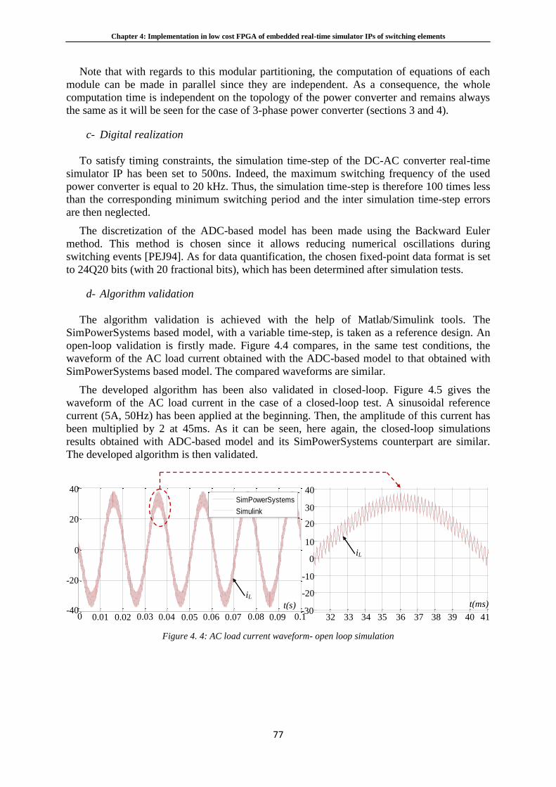
Chapter 4: Implementation in low cost FPGA of embedded real-time simulator IPs of switching elements
77
Note that with regards to this modular partitioning, the computation of equations of each
module can be made in parallel since they are independent. As a consequence, the whole
computation time is independent on the topology of the power converter and remains always
the same as it will be seen for the case of 3-phase power converter (sections 3 and 4).
c- Digital realization
To satisfy timing constraints, the simulation time-step of the DC-AC converter real-time
simulator IP has been set to 500ns. Indeed, the maximum switching frequency of the used
power converter is equal to 20 kHz. Thus, the simulation time-step is therefore 100 times less
than the corresponding minimum switching period and the inter simulation time-step errors
are then neglected.
The discretization of the ADC-based model has been made using the Backward Euler
method. This method is chosen since it allows reducing numerical oscillations during
switching events [PEJ94]. As for data quantification, the chosen fixed-point data format is set
to 24Q20 bits (with 20 fractional bits), which has been determined after simulation tests.
d- Algorithm validation
The algorithm validation is achieved with the help of Matlab/Simulink tools. The
SimPowerSystems based model, with a variable time-step, is taken as a reference design. An
open-loop validation is firstly made. Figure 4.4 compares, in the same test conditions, the
waveform of the AC load current obtained with the ADC-based model to that obtained with
SimPowerSystems based model. The compared waveforms are similar.
The developed algorithm has been also validated in closed-loop. Figure 4.5 gives the
waveform of the AC load current in the case of a closed-loop test. A sinusoidal reference
current (5A, 50Hz) has been applied at the beginning. Then, the amplitude of this current has
been multiplied by 2 at 45ms. As it can be seen, here again, the closed-loop simulations
results obtained with ADC-based model and its SimPowerSystems counterpart are similar.
The developed algorithm is then validated.
Figure 4. 4: AC load current waveform- open loop simulation
0 0.01 0.02 0.03 0.04 0.05 0.06 0.07 0.08 0.09 0.1-40
-20
0
20
40
SimPowerSystems
Simulink
0
40
-40
-20
20
0 0.01 0.02 0.03 0.04 0.05 0.06 0.07 0.08 0.09 0.1 -30
0.032 0.033 0.034 0.035 0.036 0.037 0.038 0.039 0.04 0.041-30
-20
-10
0
10
20
30
40
-20
-10
0
10
20
30
40
32 33 34 35 36 37 38 39 40 41
t(s) t(ms) iL
iL
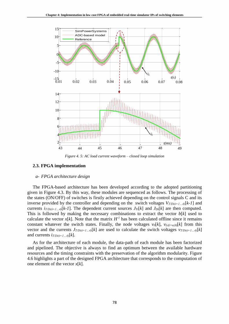
Chapter 4: Implementation in low cost FPGA of embedded real-time simulator IPs of switching elements
78
Figure 4. 5: AC load current waveform – closed loop simulation
2.3. FPGA implementation
a- FPGA architecture design
The FPGA-based architecture has been developed according to the adopted partitioning
given in Figure 4.3. By this way, these modules are sequenced as follows. The processing of
the states (ON/OFF) of switches is firstly achieved depending on the control signals C and its
inverse provided by the controller and depending on the switch voltages VT/Di(i=1…4)[k-1] and
currents iT/Di(i=1…4)[k-1]. The dependent current sources JTi[k] and JDi[k] are then computed.
This is followed by making the necessary combinations to extract the vector b[k] used to
calculate the vector x[k]. Note that the matrix H-1 has been calculated offline since it remains
constant whatever the switch states. Finally, the node voltages v0[k], vLi(i=a,b)[k] from this
vector and the currents JT/Di(i=1…4)[k] are used to calculate the switch voltages vT/Di(i=1…4)[k]
and currents iT/Di(i=1…4)[k].
As for the architecture of each module, the data-path of each module has been factorized
and pipelined. The objective is always to find an optimum between the available hardware
resources and the timing constraints with the preservation of the algorithm modularity. Figure
4.6 highlights a part of the designed FPGA architecture that corresponds to the computation of
one element of the vector x[k].
0.01 0.02 0.03 0.04 0.05 0.06 0.07 0.08-15
-10
-5
0
5
10
15
SimPowerSystems
ADC-based model
Reference
0.043 0.044 0.045 0.046 0.047 0.048 0.049
2
4
6
8
10
12
14
-15
-10
-5
0
5
10
15
0.01 0.02 0.03 0.04 0.05 0.06 0.07 0.08
43 44 45 46 47 48 49
2
4
6
8
10
12
14
t(ms)
t(s) iL
iL
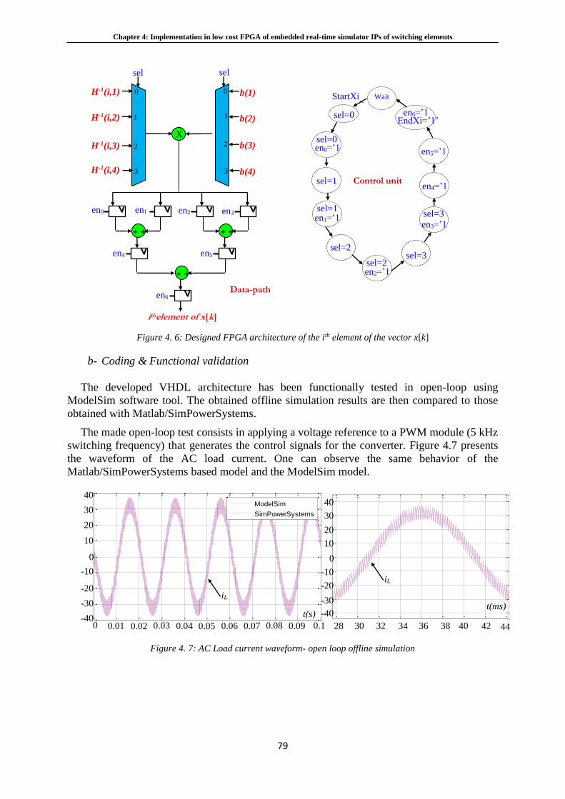
Chapter 4: Implementation in low cost FPGA of embedded real-time simulator IPs of switching elements
79
Figure 4. 6: Designed FPGA architecture of the ith element of the vector x[k]
b- Coding & Functional validation
The developed VHDL architecture has been functionally tested in open-loop using
ModelSim software tool. The obtained offline simulation results are then compared to those
obtained with Matlab/SimPowerSystems.
The made open-loop test consists in applying a voltage reference to a PWM module (5 kHz
switching frequency) that generates the control signals for the converter. Figure 4.7 presents
the waveform of the AC load current. One can observe the same behavior of the
Matlab/SimPowerSystems based model and the ModelSim model.
Figure 4. 7: AC Load current waveform- open loop offline simulation
0 0.01 0.02 0.03 0.04 0.05 0.06 0.07 0.08 0.09 0.1-40
-30
-20
-10
0
10
20
30
40
ModelSim
SimPowerSystems
0.028 0.03 0.032 0.034 0.036 0.038 0.04 0.042 0.044
-40
-30
-20
-10
0
10
20
30
40
0 0.01 0.02 0.03 0.04 0.05 0.06 0.07 0.08 0.09 0.1
t(s)
-30
-20
-10
0
10
20
30
40
-40
28 30 32 34 36 38 40 42
t(ms)
44
-30
-20
-10
0
10
20
30
40
-40
iL
iL
0
0s
el
1
1 2
1
3
X
sel sel
H-1(i,1)
Control unit
sel=0
sel=0 en0=’1
’
sel=1
EndXi=’1’
StartXi Wait
0
1
2
3
H-1(i,2)
H-1(i,3)
H-1(i,4)
Data-path
b(1)
b(2)
b(3)
b(4)
sel=1 en1=’1
’
sel=2
sel=2 en2=’1
’
en5=’1
’
sel=3
en3=’1
’
sel=3
en4=’1
’
en6=’1
’
en1 en2 en3 en0
+ +
en4
+ +
en5
+ +
en6
ithelement of x[k]
]
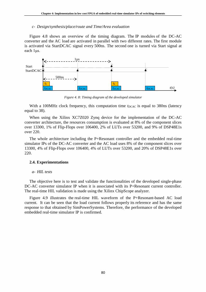
Chapter 4: Implementation in low cost FPGA of embedded real-time simulator IPs of switching elements
80
c- Design/synthesis/place/route and Time/Area evaluation
Figure 4.8 shows an overview of the timing diagram. The IP modules of the DC-AC
converter and the AC load are activated in parallel with two different rates. The first module
is activated via StartDCAC signal every 500ns. The second one is turned via Start signal at
each 1μs.
Figure 4. 8: Timing diagram of the developed simulator
With a 100MHz clock frequency, this computation time tDCAC is equal to 380ns (latency
equal to 38).
When using the Xilinx XC7Z020 Zynq device for the implementation of the DC-AC
converter architecture, the resources consumption is evaluated at 8% of the component slices
over 13300, 1% of Flip-Flops over 106400, 2% of LUTs over 53200, and 9% of DSP48E1s
over 220.
The whole architecture including the P+Resonant controller and the embedded real-time
simulator IPs of the DC-AC converter and the AC load uses 8% of the component slices over
13300, 4% of Flip-Flops over 106400, 4% of LUTs over 53200, and 20% of DSP48E1s over
220.
2.4. Experimentations
a- HIL tests
The objective here is to test and validate the functionalities of the developed single-phase
DC-AC converter simulator IP when it is associated with its P+Resonant current controller.
The real-time HIL validation is made using the Xilinx ChipScope analyzer.
Figure 4.9 illustrates the real-time HIL waveform of the P+Resonant-based AC load
current. It can be seen that the load current follows properly its reference and has the same
response to that obtained by SimPowerSystems. Therefore, the performance of the developed
embedded real-time simulator IP is confirmed.
tL
1µs
Start
tDCAC t(s)
StartDCAC
tDCAC
tL
tDCAC tDCAC
500ns
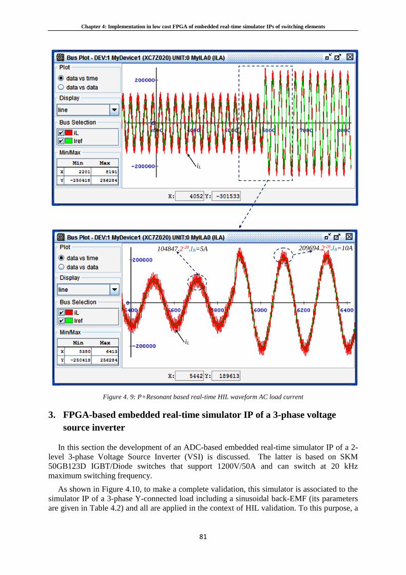
Chapter 4: Implementation in low cost FPGA of embedded real-time simulator IPs of switching elements
81
Figure 4. 9: P+Resonant based real-time HIL waveform AC load current
3. FPGA-based embedded real-time simulator IP of a 3-phase voltage
source inverter
In this section the development of an ADC-based embedded real-time simulator IP of a 2-
level 3-phase Voltage Source Inverter (VSI) is discussed. The latter is based on SKM
50GB123D IGBT/Diode switches that support 1200V/50A and can switch at 20 kHz
maximum switching frequency.
As shown in Figure 4.10, to make a complete validation, this simulator is associated to the
simulator IP of a 3-phase Y-connected load including a sinusoidal back-EMF (its parameters
are given in Table 4.2) and all are applied in the context of HIL validation. To this purpose, a
iL
104847.2-20.IB=5A
iL
209694.2-20.IB=10A
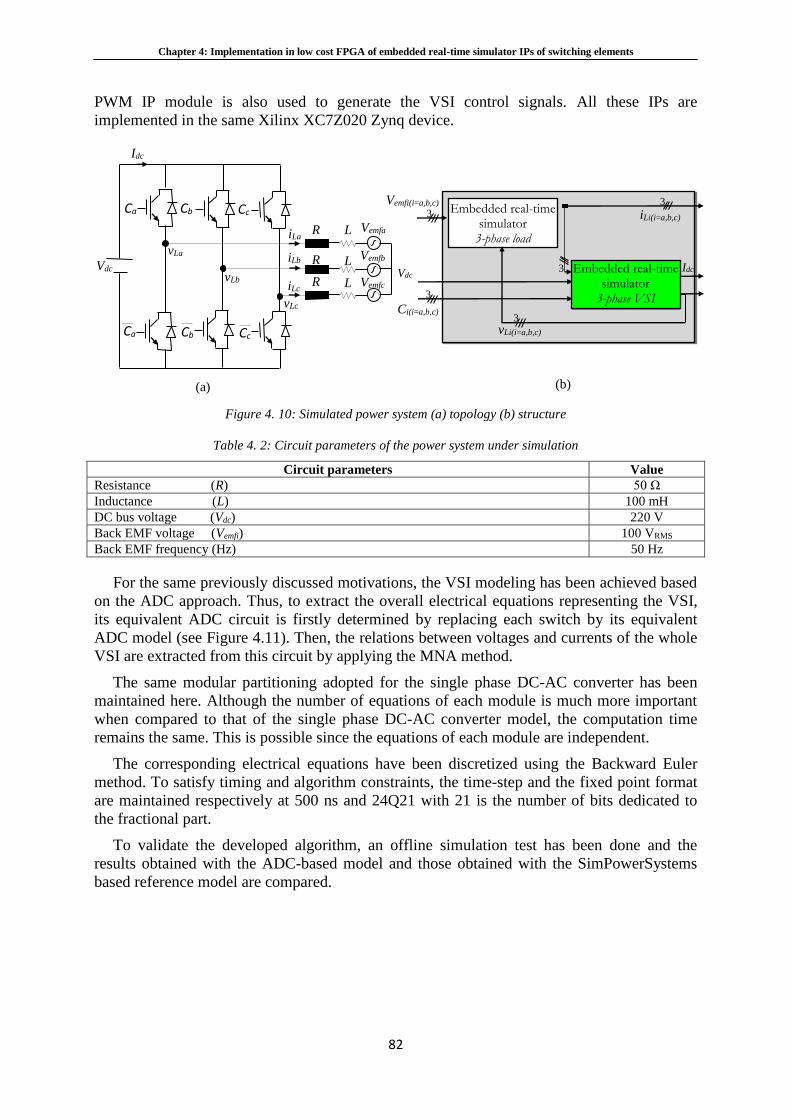
Chapter 4: Implementation in low cost FPGA of embedded real-time simulator IPs of switching elements
82
PWM IP module is also used to generate the VSI control signals. All these IPs are
implemented in the same Xilinx XC7Z020 Zynq device.
Figure 4. 10: Simulated power system (a) topology (b) structure
Table 4. 2: Circuit parameters of the power system under simulation
Circuit parameters Value
Resistance (R) 50 Ω
Inductance (L) 100 mH
DC bus voltage (Vdc) 220 V
Back EMF voltage (Vemfi) 100 VRMS
Back EMF frequency (Hz) 50 Hz
For the same previously discussed motivations, the VSI modeling has been achieved based
on the ADC approach. Thus, to extract the overall electrical equations representing the VSI,
its equivalent ADC circuit is firstly determined by replacing each switch by its equivalent
ADC model (see Figure 4.11). Then, the relations between voltages and currents of the whole
VSI are extracted from this circuit by applying the MNA method.
The same modular partitioning adopted for the single phase DC-AC converter has been
maintained here. Although the number of equations of each module is much more important
when compared to that of the single phase DC-AC converter model, the computation time
remains the same. This is possible since the equations of each module are independent.
The corresponding electrical equations have been discretized using the Backward Euler
method. To satisfy timing and algorithm constraints, the time-step and the fixed point format
are maintained respectively at 500 ns and 24Q21 with 21 is the number of bits dedicated to
the fractional part.
To validate the developed algorithm, an offline simulation test has been done and the
results obtained with the ADC-based model and those obtained with the SimPowerSystems
based reference model are compared.
(a)
Embedded real-time simulator
3-phase load
3
3 Vdc
Ci(i=a,b,c)
iLi(i=a,b,c)
vLi(i=a,b,c)
3
3
Embedded real-time simulator
3-phase VSI
3
Vemfi(i=a,b,c)
R
L
Idc
Ca
Ca
vLa
vLb
vLc
Cb
Cb
Cc
Cc
R
R
L
L
iLa
iLb
iLc
Vemfa
Vemfc
Vemfb
(b)
Vdc
Idc
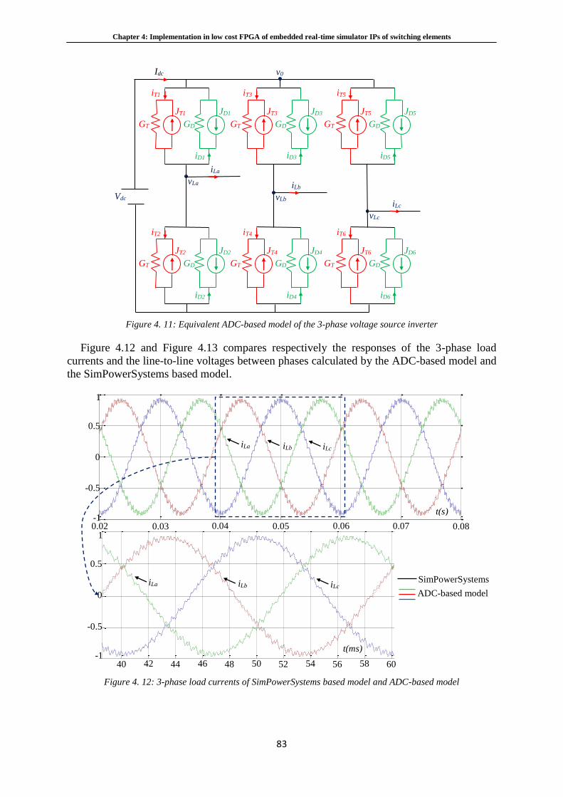
Chapter 4: Implementation in low cost FPGA of embedded real-time simulator IPs of switching elements
83
Figure 4. 11: Equivalent ADC-based model of the 3-phase voltage source inverter
Figure 4.12 and Figure 4.13 compares respectively the responses of the 3-phase load
currents and the line-to-line voltages between phases calculated by the ADC-based model and
the SimPowerSystems based model.
Figure 4. 12: 3-phase load currents of SimPowerSystems based model and ADC-based model
0.02 0.03 0.04 0.05 0.06 0.07 0.08-1
-0.5
0
0.5
1
0.04 0.042 0.044 0.046 0.048 0.05 0.052 0.054 0.056 0.058 0.06
-0.5
0
0.5
10.02 0.03 0.04 0.05 0.06 0.07 0.08
t(s)
40 42 44 46 48 50 52 54 56 60
t(ms)
iLa iLb iLc
iLa iLb iLc
-0.5
0
0.5
-1
1
-0.5
0
0.5
-1
1
SimPowerSystems
ADC-based model
58
Idc
JD1
iD1
v0
JT1
iT1
vLa
vLb
iLa
Vdc
GD GT
iD3
JT3
iT3
GD GT
JD2
iD2
JT2
iT2
GD GT
iD4
JT4
iT4
GD GT
JD3
JD4
vLc
iLb
iD5
JT5
iT5
GD GT
iD6
JT6
iT6
GD GT
JD5
JD6
iLc
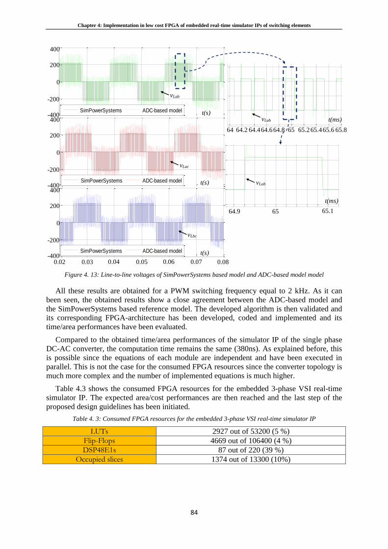
Chapter 4: Implementation in low cost FPGA of embedded real-time simulator IPs of switching elements
84
Figure 4. 13: Line-to-line voltages of SimPowerSystems based model and ADC-based model model
All these results are obtained for a PWM switching frequency equal to 2 kHz. As it can
been seen, the obtained results show a close agreement between the ADC-based model and
the SimPowerSystems based reference model. The developed algorithm is then validated and
its corresponding FPGA-architecture has been developed, coded and implemented and its
time/area performances have been evaluated.
Compared to the obtained time/area performances of the simulator IP of the single phase
DC-AC converter, the computation time remains the same (380ns). As explained before, this
is possible since the equations of each module are independent and have been executed in
parallel. This is not the case for the consumed FPGA resources since the converter topology is
much more complex and the number of implemented equations is much higher.
Table 4.3 shows the consumed FPGA resources for the embedded 3-phase VSI real-time
simulator IP. The expected area/cost performances are then reached and the last step of the
proposed design guidelines has been initiated.
Table 4. 3: Consumed FPGA resources for the embedded 3-phase VSI real-time simulator IP
LUTs 2927 out of 53200 (5 %)
Flip-Flops 4669 out of 106400 (4 %)
DSP48E1s 87 out of 220 (39 %)
Occupied slices 1374 out of 13300 (10%)
0.064 0.0642 0.0644 0.0646 0.0648 0.065 0.0652 0.0654 0.0656 0.0658-100
0
100
200
300
0.02 0.03 0.04 0.05 0.06 0.07 0.08-400
-200
0
200
400
SimPowerSystems ADC-based model
0.02 0.03 0.04 0.05 0.06 0.07 0.08-400
-200
0
200
400
SimPowerSystems ADC-based model
0.02 0.03 0.04 0.05 0.06 0.07 0.08-400
-200
0
200
400
SimPowerSystems ADC-based model
0.06490.06490.06490.06490.065 0.065 0.065 0.065 0.065 0.06510.0651
-100
0
100
200
300
0.02 0.03 0.04 0.05 0.06 0.07 0.08
t(s)
t(s)
t(s)
vLab
vLac
vLbc
vLab
vLab
0
200
400
-200
-400
0
200
400
-200
-400
0
200
400
-200
-400
64.2
4
64.4
4
64.6
4
64.8
4
65 65.2 65.4
4
65.6 65.8 64
t(ms)
64.9 65 65.1
t(ms)
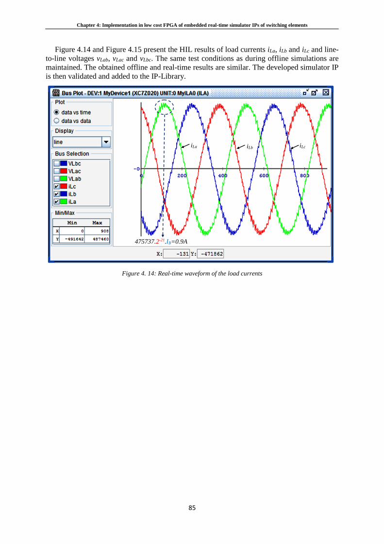
Chapter 4: Implementation in low cost FPGA of embedded real-time simulator IPs of switching elements
85
Figure 4.14 and Figure 4.15 present the HIL results of load currents iLa, iLb and iLc and line-
to-line voltages vLab, vLac and vLbc. The same test conditions as during offline simulations are
maintained. The obtained offline and real-time results are similar. The developed simulator IP
is then validated and added to the IP-Library.
Figure 4. 14: Real-time waveform of the load currents
iLa
475737.2-21.IB=0.9A
iLb iLc
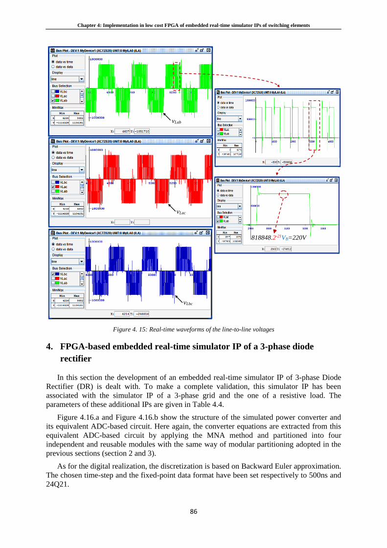
Chapter 4: Implementation in low cost FPGA of embedded real-time simulator IPs of switching elements
86
Figure 4. 15: Real-time waveforms of the line-to-line voltages
4. FPGA-based embedded real-time simulator IP of a 3-phase diode
rectifier
In this section the development of an embedded real-time simulator IP of 3-phase Diode
Rectifier (DR) is dealt with. To make a complete validation, this simulator IP has been
associated with the simulator IP of a 3-phase grid and the one of a resistive load. The
parameters of these additional IPs are given in Table 4.4.
Figure 4.16.a and Figure 4.16.b show the structure of the simulated power converter and
its equivalent ADC-based circuit. Here again, the converter equations are extracted from this
equivalent ADC-based circuit by applying the MNA method and partitioned into four
independent and reusable modules with the same way of modular partitioning adopted in the
previous sections (section 2 and 3).
As for the digital realization, the discretization is based on Backward Euler approximation.
The chosen time-step and the fixed-point data format have been set respectively to 500ns and
24Q21.
818848.2-21VB=220V
vLab
vLac
vLbc
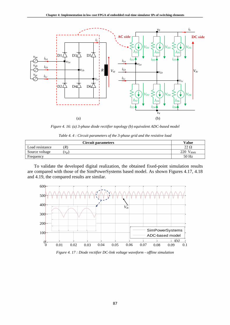
Chapter 4: Implementation in low cost FPGA of embedded real-time simulator IPs of switching elements
87
Figure 4. 16: (a) 3-phase diode rectifier topology (b) equivalent ADC-based model
Table 4. 4 : Circuit parameters of the 3-phase grid and the resistive load
Circuit parameters Value
Load resistance (R) 22 Ω
Source voltage (vgi) 220 VRMS
Frequency 50 Hz
To validate the developed digital realization, the obtained fixed-point simulation results
are compared with those of the SimPowerSystems based model. As shown Figures 4.17, 4.18
and 4.19, the compared results are similar.
Figure 4. 17 : Diode rectifier DC-link voltage waveform - offline simulation
0 0.01 0.02 0.03 0.04 0.05 0.06 0.07 0.08 0.09 0.10
100
200
300
400
500
600
SimPowerSystems
ADC-based model
0.01 0.02 0.03 0.04 0.05 0.06 0.07 0.08 0.09 0.1 0 0
100
200
300
400
500
600
t(s)
Vdc
0.064 0.066 0.068 0.07 0.072 0.074 0.076 0.078
400
450
500
550
600
SimPowerSystems
ADC-based model
iLa
vga
R
vgb
vgc
iLb
iLc
vLa
vLb
vLc
iL
Vdc
D1
D2
D3
D4
D5
D6
JD1
iD1
JD2
JD3
JD4
JD5
JD6
iD3 iD5
iD2 iD4 iD6
iLa
iLb
iLc
vLa
vLb
vLc
iL v0
v4
VD1
VD2
VD3
VD4
VD5
VD6
Vdc
(a)
(b)
AC side
DC side
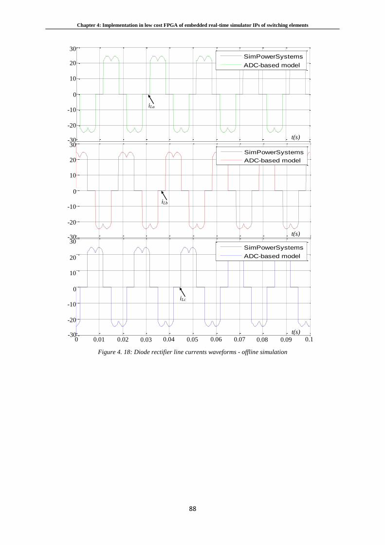
Chapter 4: Implementation in low cost FPGA of embedded real-time simulator IPs of switching elements
88
Figure 4. 18: Diode rectifier line currents waveforms - offline simulation
0 0.01 0.02 0.03 0.04 0.05 0.06 0.07 0.08 0.09 0.1-30
-20
-10
0
10
20
30
SimPowerSystems
ADC-based model
0 0.01 0.02 0.03 0.04 0.05 0.06 0.07 0.08 0.09 0.1-30
-20
-10
0
10
20
30
SimPowerSystems
ADC-based model
0 0.01 0.02 0.03 0.04 0.05 0.06 0.07 0.08 0.09 0.1-30
-20
-10
0
10
20
30
SimPowerSystems
ADC-based model
0.01 0.02 0.03 0.04 0.05 0.06 0.07 0.08 0.09 0.1 0
t(s)
t(s)
t(s)
-30
-20
-10
0
10
20
30
-30
-20
-10
0
10
20
30
-30
-20
-10
0
10
20
30
iLc
iLb
iLa
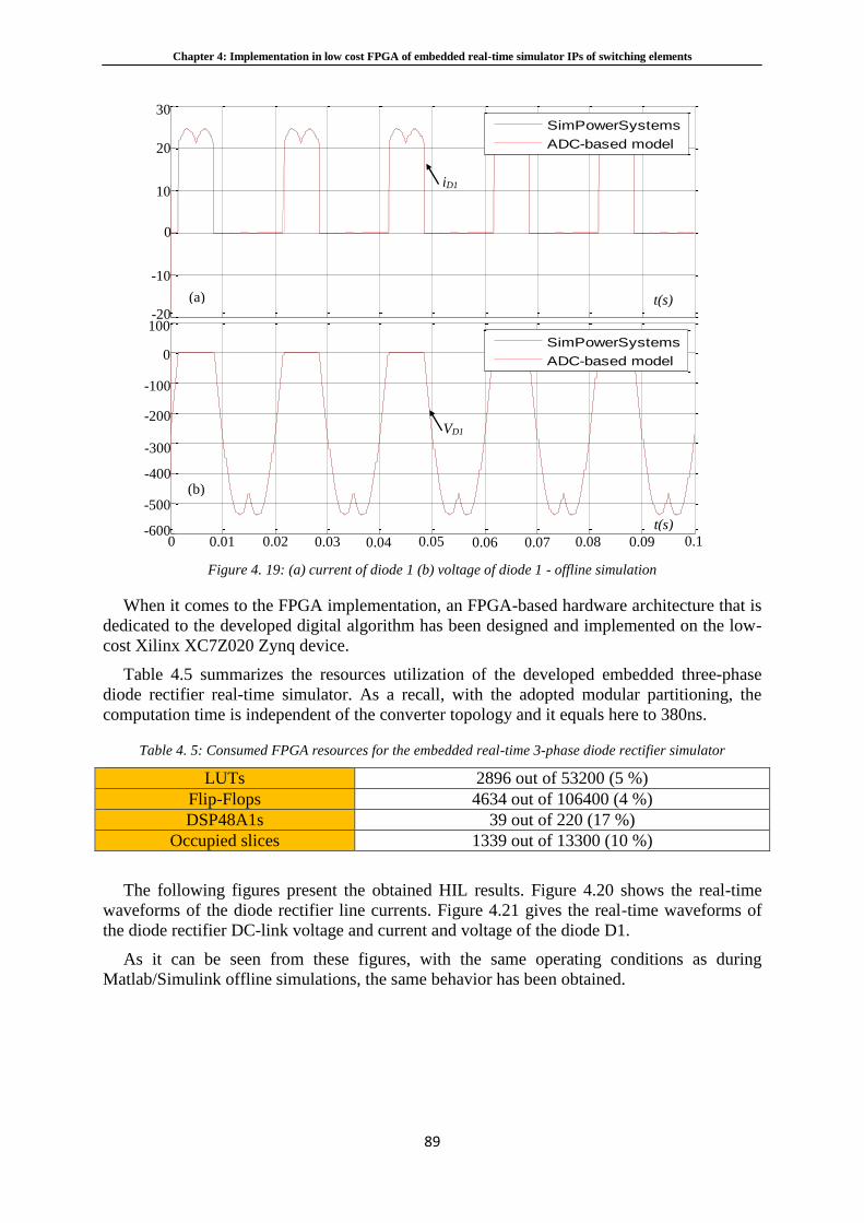
Chapter 4: Implementation in low cost FPGA of embedded real-time simulator IPs of switching elements
89
Figure 4. 19: (a) current of diode 1 (b) voltage of diode 1 - offline simulation
When it comes to the FPGA implementation, an FPGA-based hardware architecture that is
dedicated to the developed digital algorithm has been designed and implemented on the low-
cost Xilinx XC7Z020 Zynq device.
Table 4.5 summarizes the resources utilization of the developed embedded three-phase
diode rectifier real-time simulator. As a recall, with the adopted modular partitioning, the
computation time is independent of the converter topology and it equals here to 380ns.
Table 4. 5: Consumed FPGA resources for the embedded real-time 3-phase diode rectifier simulator
LUTs 2896 out of 53200 (5 %)
Flip-Flops 4634 out of 106400 (4 %)
DSP48A1s 39 out of 220 (17 %)
Occupied slices 1339 out of 13300 (10 %)
The following figures present the obtained HIL results. Figure 4.20 shows the real-time
waveforms of the diode rectifier line currents. Figure 4.21 gives the real-time waveforms of
the diode rectifier DC-link voltage and current and voltage of the diode D1.
As it can be seen from these figures, with the same operating conditions as during
Matlab/Simulink offline simulations, the same behavior has been obtained.
0 0.01 0.02 0.03 0.04 0.05 0.06 0.07 0.08 0.09 0.1-20
-10
0
10
20
30
SimPowerSystems
ADC-based model
0 0.01 0.02 0.03 0.04 0.05 0.06 0.07 0.08 0.09 0.1-600
-500
-400
-300
-200
-100
0
100
SimPowerSystems
ADC-based model
0.01 0.02 0.03 0.04 0.05 0.06 0.07 0.08 0.09 0.1
t(s)
t(s)
0 -600
-500
-400
-300
-200
-100
0
100 -20
-10
0
10
20
30
(a)
(b)
iD1
VD1
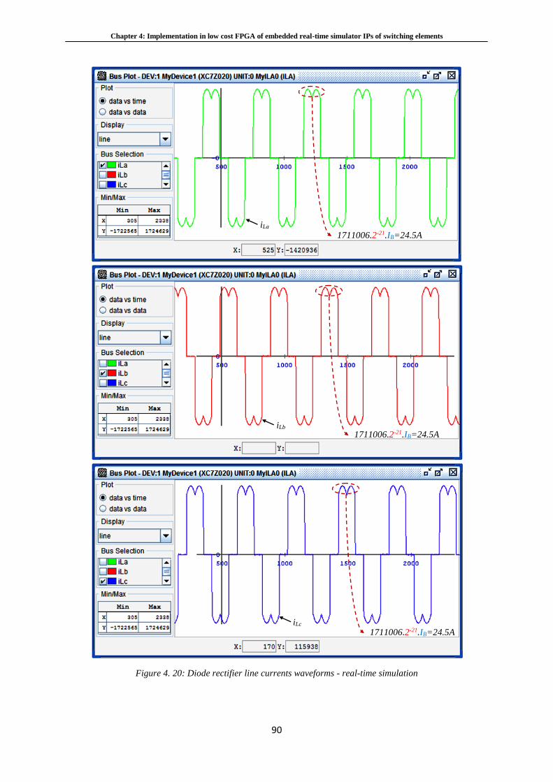
Chapter 4: Implementation in low cost FPGA of embedded real-time simulator IPs of switching elements
90
Figure 4. 20: Diode rectifier line currents waveforms - real-time simulation
iLa 1711006.2-21.IB=24.5A
iLb
iLc
1711006.2-21.IB=24.5A
1711006.2-21.IB=24.5A
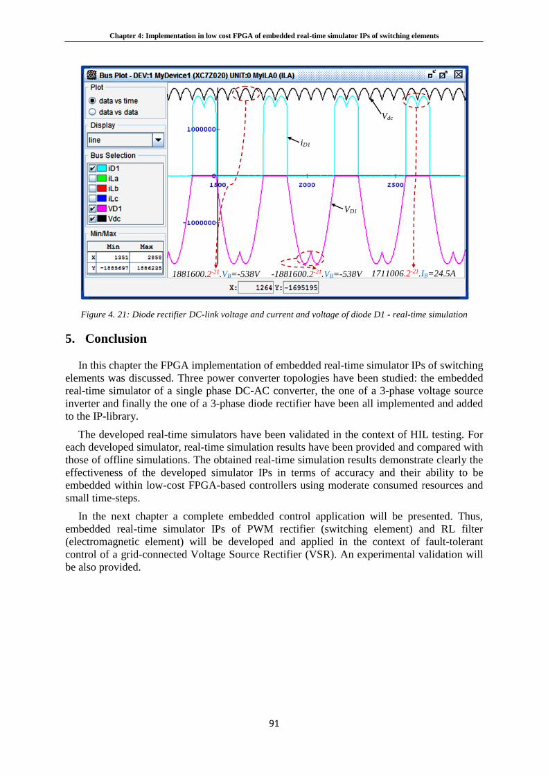
Chapter 4: Implementation in low cost FPGA of embedded real-time simulator IPs of switching elements
91
Figure 4. 21: Diode rectifier DC-link voltage and current and voltage of diode D1 - real-time simulation
5. Conclusion
In this chapter the FPGA implementation of embedded real-time simulator IPs of switching
elements was discussed. Three power converter topologies have been studied: the embedded
real-time simulator of a single phase DC-AC converter, the one of a 3-phase voltage source
inverter and finally the one of a 3-phase diode rectifier have been all implemented and added
to the IP-library.
The developed real-time simulators have been validated in the context of HIL testing. For
each developed simulator, real-time simulation results have been provided and compared with
those of offline simulations. The obtained real-time simulation results demonstrate clearly the
effectiveness of the developed simulator IPs in terms of accuracy and their ability to be
embedded within low-cost FPGA-based controllers using moderate consumed resources and
small time-steps.
In the next chapter a complete embedded control application will be presented. Thus,
embedded real-time simulator IPs of PWM rectifier (switching element) and RL filter
(electromagnetic element) will be developed and applied in the context of fault-tolerant
control of a grid-connected Voltage Source Rectifier (VSR). An experimental validation will
be also provided.
iD1
VD1
Vdc
1711006.2-21.IB=24.5A -1881600.2-21.VB=-538V 1881600.2-21.VB=-538V
Chapter 5: Embedded Real-Time Simulator IPs of PWM Rectifier and 3-phase RL-Filter
Application to a Fault-Tolerant Control of a Grid-Connected Voltage Source Rectifier
92
Chapter 5
Embedded Real-Time Simulator IPs of PWM
Rectifier and 3-phase RL-Filter
Application to a Fault-Tolerant Control of a Grid-
Connected Voltage Source Rectifier
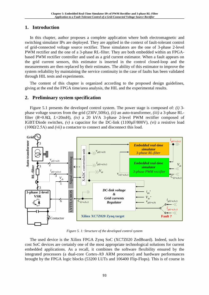
Chapter 5: Embedded Real-Time Simulator IPs of PWM Rectifier and 3-phase RL-Filter
Application to a Fault-Tolerant Control of a Grid-Connected Voltage Source Rectifier
93
1. Introduction
In this chapter, author proposes a complete application where both electromagnetic and
switching simulator IPs are deployed. They are applied in the context of fault-tolerant control
of grid-connected voltage source rectifier. These simulators are the one of 3-phase 2-level
PWM rectifier and the one of a 3-phase RL-filter. They are both embedded within an FPGA-
based PWM rectifier controller and used as a grid current estimator. When a fault appears on
the grid current sensors, this estimator is inserted in the control closed-loop and the
measurements are then replaced by their estimates. The ability of this estimator to improve the
system reliability by maintaining the service continuity in the case of faults has been validated
through HIL tests and experiments.
The content of this chapter is organized according to the proposed design guidelines,
giving at the end the FPGA time/area analysis, the HIL and the experimental results.
2. Preliminary system specification
Figure 5.1 presents the developed control system. The power stage is composed of: (i) 3-
phase voltage sources from the grid (230V,50Hz), (ii) an auto-transformer, (iii) a 3-phase RL-
filter (R=0.8Ω, L=20mH), (iv) a 20 kVA 3-phase 2-level PWM rectifier composed of
IGBT/Diode switches, (v) a capacitor for the DC-link (1100µF/800V), (vi) a resistive load
(100Ω/2.5A) and (vii) a contactor to connect and disconnect this load.
Figure 5. 1: Structure of the developed control system
The used device is the Xilinx FPGA Zynq SoC (XC7Z020 ZedBoard). Indeed, such low
cost SoC devices are certainly one of the most appropriate technological solutions for current
embedded applications. As a recall, it combines the software flexibility ensured by the
integrated processors (a dual-core Cortex-A9 ARM processor) and hardware performances
brought by the FPGA logic blocks (53200 LUTs and 106400 Flip-Flops). This is of course in
3
vgi(i=a,b)
Au
to-t
ran
sfo
rmer
RL
-fil
ter
3-phase 2-level
VSR
Grid
L
VT
TL
/CM
OS
igi(i=a,b,c)
Sig
nal
co
nd
itio
nin
g
Vdc
3
3
2
3
1
6
XA
DC
co
nv
ersi
on
un
it
Embedded real-time
simulator 3-phase RL-filter
Embedded real-time
simulator
3-phase PWM rectifier
DC-link voltage
&
Grid currents
Regulator
Xilinx XC7Z020 Zynq target
vgi(i=a,b)
igi(i=a,b,c)
Vdc
vgi(i=a,b)
Fault ?
igi(i=a,b,c)
îgi(i=a,b,c)
vLi(i=a,b,c)
îgi(i=a,b,c)
Ci(i=a,b,c)
Vdc
Contactor
Ci(i=a,b,c)
V
dc*
igq
*
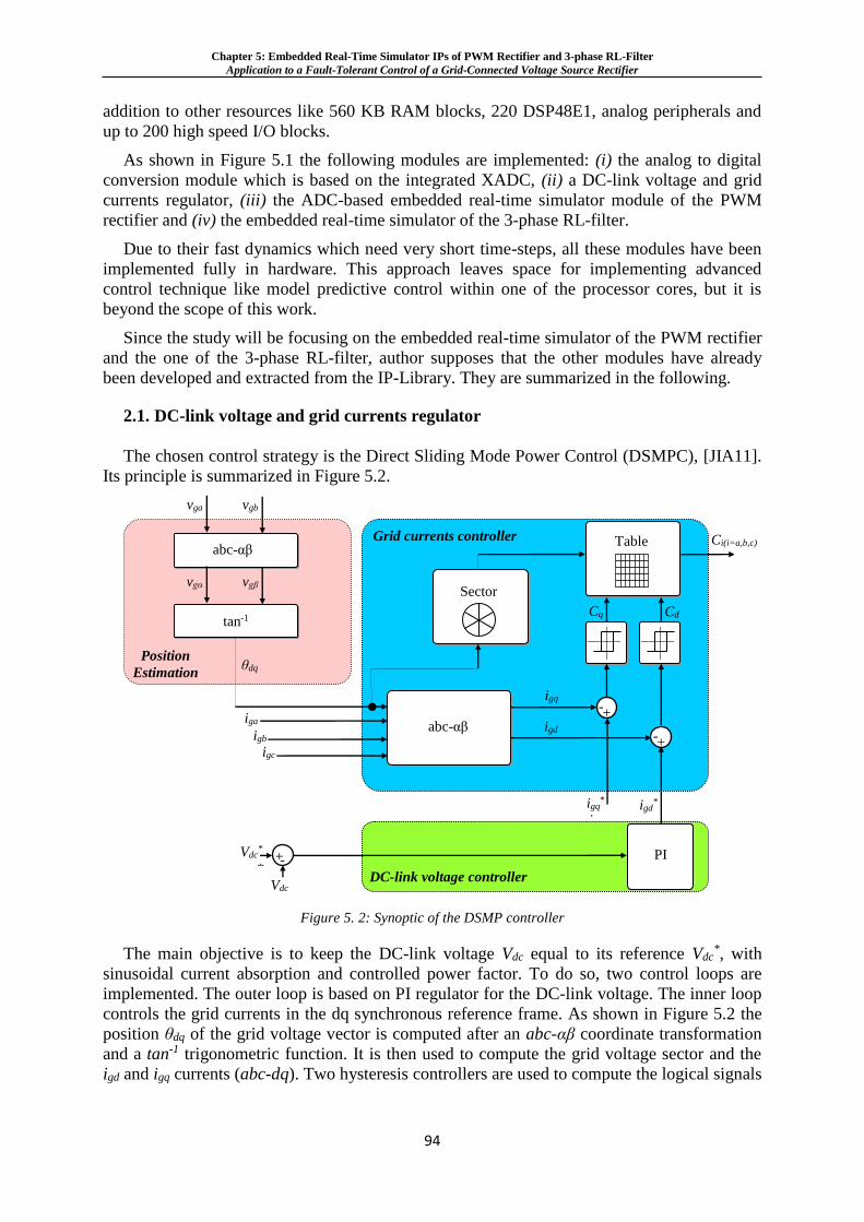
Chapter 5: Embedded Real-Time Simulator IPs of PWM Rectifier and 3-phase RL-Filter
Application to a Fault-Tolerant Control of a Grid-Connected Voltage Source Rectifier
94
addition to other resources like 560 KB RAM blocks, 220 DSP48E1, analog peripherals and
up to 200 high speed I/O blocks.
As shown in Figure 5.1 the following modules are implemented: (i) the analog to digital
conversion module which is based on the integrated XADC, (ii) a DC-link voltage and grid
currents regulator, (iii) the ADC-based embedded real-time simulator module of the PWM
rectifier and (iv) the embedded real-time simulator of the 3-phase RL-filter.
Due to their fast dynamics which need very short time-steps, all these modules have been
implemented fully in hardware. This approach leaves space for implementing advanced
control technique like model predictive control within one of the processor cores, but it is
beyond the scope of this work.
Since the study will be focusing on the embedded real-time simulator of the PWM rectifier
and the one of the 3-phase RL-filter, author supposes that the other modules have already
been developed and extracted from the IP-Library. They are summarized in the following.
2.1. DC-link voltage and grid currents regulator
The chosen control strategy is the Direct Sliding Mode Power Control (DSMPC), [JIA11].
Its principle is summarized in Figure 5.2.
Figure 5. 2: Synoptic of the DSMP controller
The main objective is to keep the DC-link voltage Vdc equal to its reference Vdc*, with
sinusoidal current absorption and controlled power factor. To do so, two control loops are
implemented. The outer loop is based on PI regulator for the DC-link voltage. The inner loop
controls the grid currents in the dq synchronous reference frame. As shown in Figure 5.2 the
position θdq of the grid voltage vector is computed after an abc-αβ coordinate transformation
and a tan-1 trigonometric function. It is then used to compute the grid voltage sector and the
igd and igq currents (abc-dq). Two hysteresis controllers are used to compute the logical signals
Position
Estimation
DC-link voltage controller
Grid currents controller abc-αβ
tan-1
vga vgb
vgα vgβ
abc-αβ iga
igb igc
θdq
Sector
Table
PI + - Vdc
*
Vdc
* Vdc
- +
- +
igq
igd
igq*
igq
*
igd*
Ci(i=a,b,c)
Cq Cd
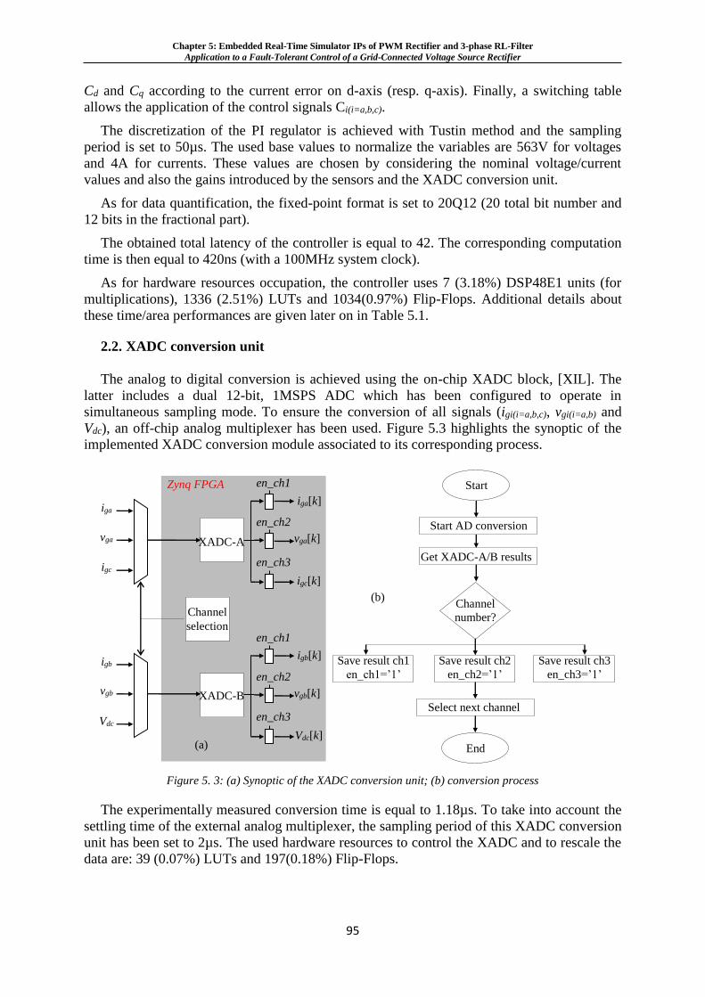
Chapter 5: Embedded Real-Time Simulator IPs of PWM Rectifier and 3-phase RL-Filter
Application to a Fault-Tolerant Control of a Grid-Connected Voltage Source Rectifier
95
Cd and Cq according to the current error on d-axis (resp. q-axis). Finally, a switching table
allows the application of the control signals Ci(i=a,b,c).
The discretization of the PI regulator is achieved with Tustin method and the sampling
period is set to 50µs. The used base values to normalize the variables are 563V for voltages
and 4A for currents. These values are chosen by considering the nominal voltage/current
values and also the gains introduced by the sensors and the XADC conversion unit.
As for data quantification, the fixed-point format is set to 20Q12 (20 total bit number and
12 bits in the fractional part).
The obtained total latency of the controller is equal to 42. The corresponding computation
time is then equal to 420ns (with a 100MHz system clock).
As for hardware resources occupation, the controller uses 7 (3.18%) DSP48E1 units (for
multiplications), 1336 (2.51%) LUTs and 1034(0.97%) Flip-Flops. Additional details about
these time/area performances are given later on in Table 5.1.
2.2. XADC conversion unit
The analog to digital conversion is achieved using the on-chip XADC block, [XIL]. The
latter includes a dual 12-bit, 1MSPS ADC which has been configured to operate in
simultaneous sampling mode. To ensure the conversion of all signals (igi(i=a,b,c), vgi(i=a,b) and
Vdc), an off-chip analog multiplexer has been used. Figure 5.3 highlights the synoptic of the
implemented XADC conversion module associated to its corresponding process.
Figure 5. 3: (a) Synoptic of the XADC conversion unit; (b) conversion process
The experimentally measured conversion time is equal to 1.18µs. To take into account the
settling time of the external analog multiplexer, the sampling period of this XADC conversion
unit has been set to 2µs. The used hardware resources to control the XADC and to rescale the
data are: 39 (0.07%) LUTs and 197(0.18%) Flip-Flops.
Channel
selection
XADC-A
XADC-B
en_ch1
iga[k]
vga[k]
igc[k]
en_ch3
en_ch2
en_ch1
igb[k]
vgb[k]
Vdc[k]
en_ch3
en_ch2
(a)
Start
Start AD conversion
Get XADC-A/B results
Channel
number?
Save result ch1
en_ch1=’1’
Save result ch2
en_ch2=’1’
Save result ch3
en_ch3=’1’
Select next channel
End
(b)
Zynq FPGA
iga
vga
igc
igb
vgb
Vdc
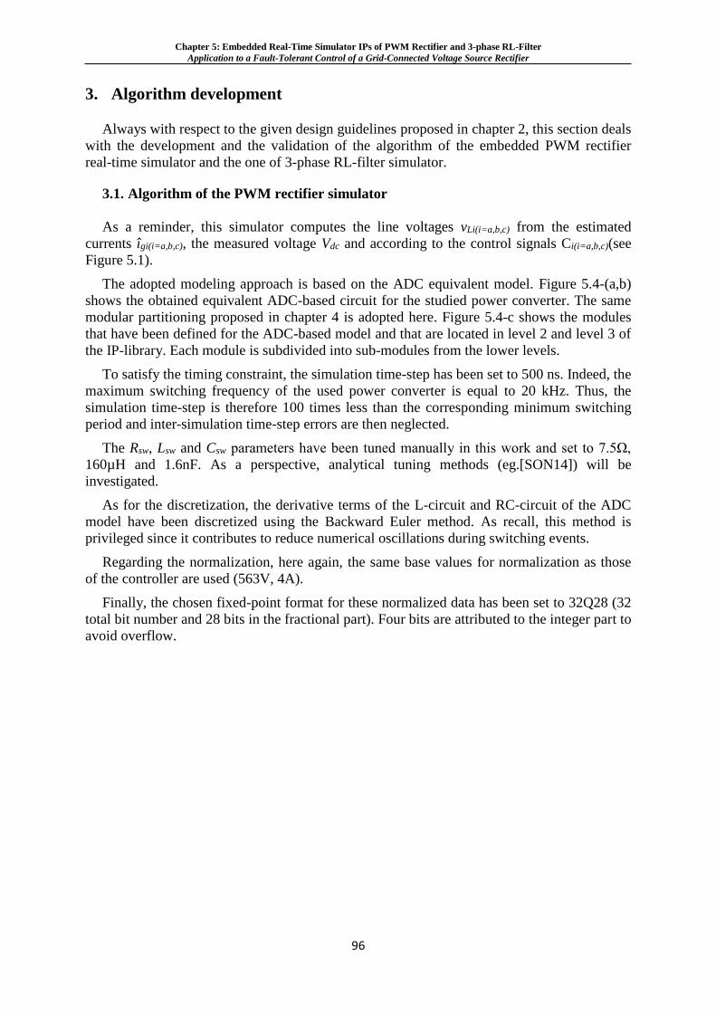
Chapter 5: Embedded Real-Time Simulator IPs of PWM Rectifier and 3-phase RL-Filter
Application to a Fault-Tolerant Control of a Grid-Connected Voltage Source Rectifier
96
3. Algorithm development
Always with respect to the given design guidelines proposed in chapter 2, this section deals
with the development and the validation of the algorithm of the embedded PWM rectifier
real-time simulator and the one of 3-phase RL-filter simulator.
3.1. Algorithm of the PWM rectifier simulator
As a reminder, this simulator computes the line voltages vLi(i=a,b,c) from the estimated
currents îgi(i=a,b,c), the measured voltage Vdc and according to the control signals Ci(i=a,b,c)(see
Figure 5.1).
The adopted modeling approach is based on the ADC equivalent model. Figure 5.4-(a,b)
shows the obtained equivalent ADC-based circuit for the studied power converter. The same
modular partitioning proposed in chapter 4 is adopted here. Figure 5.4-c shows the modules
that have been defined for the ADC-based model and that are located in level 2 and level 3 of
the IP-library. Each module is subdivided into sub-modules from the lower levels.
To satisfy the timing constraint, the simulation time-step has been set to 500 ns. Indeed, the
maximum switching frequency of the used power converter is equal to 20 kHz. Thus, the
simulation time-step is therefore 100 times less than the corresponding minimum switching
period and inter-simulation time-step errors are then neglected.
The Rsw, Lsw and Csw parameters have been tuned manually in this work and set to 7.5Ω,
160µH and 1.6nF. As a perspective, analytical tuning methods (eg.[SON14]) will be
investigated.
As for the discretization, the derivative terms of the L-circuit and RC-circuit of the ADC
model have been discretized using the Backward Euler method. As recall, this method is
privileged since it contributes to reduce numerical oscillations during switching events.
Regarding the normalization, here again, the same base values for normalization as those
of the controller are used (563V, 4A).
Finally, the chosen fixed-point format for these normalized data has been set to 32Q28 (32
total bit number and 28 bits in the fractional part). Four bits are attributed to the integer part to
avoid overflow.
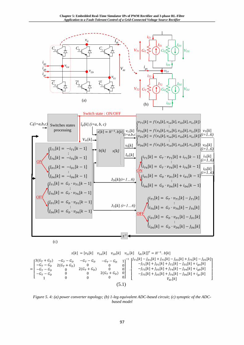
Chapter 5: Embedded Real-Time Simulator IPs of PWM Rectifier and 3-phase RL-Filter
Application to a Fault-Tolerant Control of a Grid-Connected Voltage Source Rectifier
97
Figure 5. 4: (a) power converter topology; (b) 1-leg equivalent ADC-based circuit; (c) synoptic of the ADC-
based model
𝑥[𝑘] = 𝐻−1. 𝑏[𝑘]
b[k] x[k]
JTi[k] (i=1…6)
JDi[k](i=1…6)
vLi[k] (i=a,b,c)
Vdc[k]
Idc[k]
v0[k]
z-1
Switches states
processing
vDi[k] (i=1..6)
iTi[k] (i=1..6)
iDi[k] (i=1..6)
OFF
𝑖𝑇1[𝑘] = 𝐺𝑇 ∙ 𝑣𝑇1[𝑘] − 𝐽𝑇1[𝑘]
:𝑖𝑇6[𝑘] = 𝐺𝑇 ∙ 𝑣𝑇6[𝑘] − 𝐽𝑇6[𝑘]
𝑖𝐷1[𝑘] = 𝐺𝐷 ∙ 𝑣𝐷1[𝑘] − 𝐽𝐷1[𝑘]
:𝑖𝐷6[𝑘] = 𝐺𝐷 ∙ 𝑣𝐷6[𝑘] − 𝐽𝐷6[𝑘]
𝑖𝑇1[𝑘] = 𝐺𝑇 ∙ 𝑣𝑇1[𝑘] + 𝑖𝑇1[𝑘 − 1]
:𝑖𝑇6[𝑘] = 𝐺𝑇 ∙ 𝑣𝑇6[𝑘] + 𝑖𝑇6[𝑘 − 1]
𝑖𝐷1[𝑘] = 𝐺𝐷 ∙ 𝑣𝐷1[𝑘] + 𝑖𝐷1[𝑘 − 1]
:𝑖𝐷6[𝑘] = 𝐺𝐷 ∙ 𝑣𝐷6[𝑘] + 𝑖𝐷6[𝑘 − 1]
𝐽𝑇1[𝑘] = −𝑖𝑇1[𝑘 − 1]
:𝐽𝑇6[𝑘] = −𝑖𝑇6[𝑘 − 1]
𝐽𝐷1[𝑘] = −𝑖𝐷1[𝑘 − 1]
:𝐽𝐷6[𝑘] = −𝑖𝐷6[𝑘 − 1]
𝐽𝑇1[𝑘] = 𝐺𝑇 ∙ 𝑣𝑇1[𝑘 − 1]
:𝐽𝑇6[𝑘] = 𝐺𝑇 ∙ 𝑣𝑇6[𝑘 − 1]
𝐽𝐷1[𝑘] = 𝐺𝐷 ∙ 𝑣𝐷1[𝑘 − 1]
:𝐽𝐷6[𝑘] = 𝐺𝐷 ∙ 𝑣𝐷6[𝑘 − 1]
ON
vTi[k] (i=1..6)
𝑣𝑇1[𝑘] = 𝑓(𝑣0[𝑘], 𝑣𝐿𝑎[𝑘], 𝑣𝐿𝑏[𝑘], 𝑣𝐿𝑐[𝑘])
:𝑣𝑇6[𝑘] = 𝑓(𝑣0[𝑘], 𝑣𝐿𝑎[𝑘], 𝑣𝐿𝑏[𝑘], 𝑣𝐿𝑐[𝑘])
𝑣𝐷1[𝑘] = 𝑓(𝑣0[𝑘], 𝑣𝐿𝑎[𝑘], 𝑣𝐿𝑏[𝑘], 𝑣𝐿𝑐[𝑘])
:𝑣𝐷6[𝑘] = 𝑓(𝑣0[𝑘], 𝑣𝐿𝑎[𝑘], 𝑣𝐿𝑏[𝑘], 𝑣𝐿𝑐[𝑘])
Switch state : ON/OFF
ON
OFF
Ci(i=a,b,c) îgi[k] (i=a, b, c)
Idc
vLa
Ca
iga
vLb
vLc
igb
igc
Cb C
c
Ca C
b
v0
Vdc
JD1
iD1
JT1
iT1
vLa
GD GT
JD2
iD2
JT2
iT2
GD GT
iga
VD1
VD2
VT1
VT2
𝑥[𝑘] = [𝑣0[𝑘] 𝑣𝐿𝑎[𝑘] 𝑣𝐿𝑏[𝑘] 𝑣𝐿𝑐[𝑘] 𝐼𝑑𝑐[𝑘]]𝑇 = 𝐻−1. 𝑏[𝑘]
=
[ 3(𝐺𝑇 + 𝐺𝐷)−𝐺𝑇 − 𝐺𝐷−𝐺𝑇 − 𝐺𝐷−𝐺𝑇 − 𝐺𝐷
1
−𝐺𝑇 − 𝐺𝐷2(𝐺𝑇 + 𝐺𝐷)
000
−𝐺𝑇 − 𝐺𝐷0
2(𝐺𝑇 + 𝐺𝐷)00
−𝐺𝑇 − 𝐺𝐷00
2(𝐺𝑇 + 𝐺𝐷)0
10000] −1
.
[ 𝐽𝑇1[𝑘] − 𝐽𝐷1[𝑘] + 𝐽𝑇3[𝑘] − 𝐽𝐷3[𝑘] + 𝐽𝑇5[𝑘] − 𝐽𝐷5[𝑘]
−𝐽𝑇1[𝑘] + 𝐽𝐷1[𝑘] + 𝐽𝑇2[𝑘] − 𝐽𝐷2[𝑘] + 𝑖𝑔𝑎[𝑘]
−𝐽𝑇3[𝑘] + 𝐽𝐷3[𝑘] + 𝐽𝑇4[𝑘] − 𝐽𝐷4[𝑘] + 𝑖𝑔𝑏[𝑘]
−𝐽𝑇5[𝑘] + 𝐽𝐷5[𝑘] + 𝐽𝑇6[𝑘] − 𝐽𝐷6[𝑘] + 𝑖𝑔𝑐[𝑘]
𝑉𝑑𝑐[𝑘] ]
(5.1)
(a) (b)
(c)
Cc
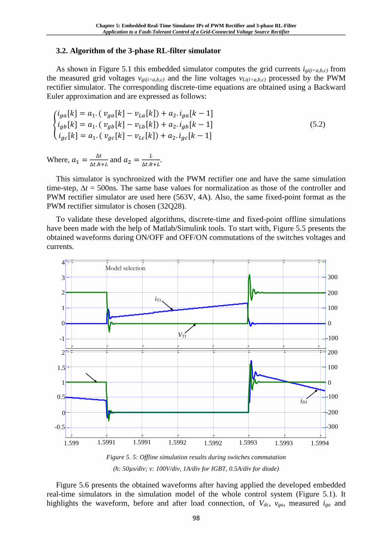
Chapter 5: Embedded Real-Time Simulator IPs of PWM Rectifier and 3-phase RL-Filter
Application to a Fault-Tolerant Control of a Grid-Connected Voltage Source Rectifier
98
3.2. Algorithm of the 3-phase RL-filter simulator
As shown in Figure 5.1 this embedded simulator computes the grid currents igi(i=a,b,c) from
the measured grid voltages vgi(i=a,b,c) and the line voltages vLi(i=a,b,c) processed by the PWM
rectifier simulator. The corresponding discrete-time equations are obtained using a Backward
Euler approximation and are expressed as follows:
𝑖𝑔𝑎[𝑘] = 𝑎1. ( 𝑣𝑔𝑎[𝑘] − 𝑣𝐿𝑎[𝑘]) + 𝑎2. 𝑖𝑔𝑎[𝑘 − 1]
𝑖𝑔𝑏[𝑘] = 𝑎1. ( 𝑣𝑔𝑏[𝑘] − 𝑣𝐿𝑏[𝑘]) + 𝑎2. 𝑖𝑔𝑏[𝑘 − 1]
𝑖𝑔𝑐[𝑘] = 𝑎1. ( 𝑣𝑔𝑐[𝑘] − 𝑣𝐿𝑐[𝑘]) + 𝑎2. 𝑖𝑔𝑐[𝑘 − 1]
(5.2)
Where, 𝑎1 =∆𝑡
∆𝑡.𝑅+𝐿 and 𝑎2 =
𝐿
∆𝑡.𝑅+𝐿.
This simulator is synchronized with the PWM rectifier one and have the same simulation
time-step, ∆t = 500ns. The same base values for normalization as those of the controller and
PWM rectifier simulator are used here (563V, 4A). Also, the same fixed-point format as the
PWM rectifier simulator is chosen (32Q28).
To validate these developed algorithms, discrete-time and fixed-point offline simulations
have been made with the help of Matlab/Simulink tools. To start with, Figure 5.5 presents the
obtained waveforms during ON/OFF and OFF/ON commutations of the switches voltages and
currents.
Figure 5. 5: Offline simulation results during switches commutation
(h: 50µs/div; v: 100V/div, 1A/div for IGBT, 0.5A/div for diode)
Figure 5.6 presents the obtained waveforms after having applied the developed embedded
real-time simulators in the simulation model of the whole control system (Figure 5.1). It
highlights the waveform, before and after load connection, of Vdc, vga, measured iga and
1.599 1.5991 1.5991 1.5992 1.5992 1.5993 1.5993 1.5994
-1
0
1
2
3
4
1.599 1.5991 1.5991 1.5992 1.5992 1.5993 1.5993 1.5994
-100
0
100
200
300
400
1.599 1.5991 1.5991 1.5992 1.5992 1.5993 1.5993 1.5994
-0.5
0
0.5
1
1.5
2
1.599 1.5991 1.5991 1.5992 1.5992 1.5993 1.5993 1.5994
-300
-200
-100
0
100
200
Model selection
1.599 1.5991 1.5991 1.5992 1.5992 1.5993 1.5993 1.5994
300
200
100
0
-100
200
100
0
-100
-200
-300
4
3
2
1
0
-1
2
1.5
0.5
-0.5
1
0
VT1
iD1
iT1
VD1
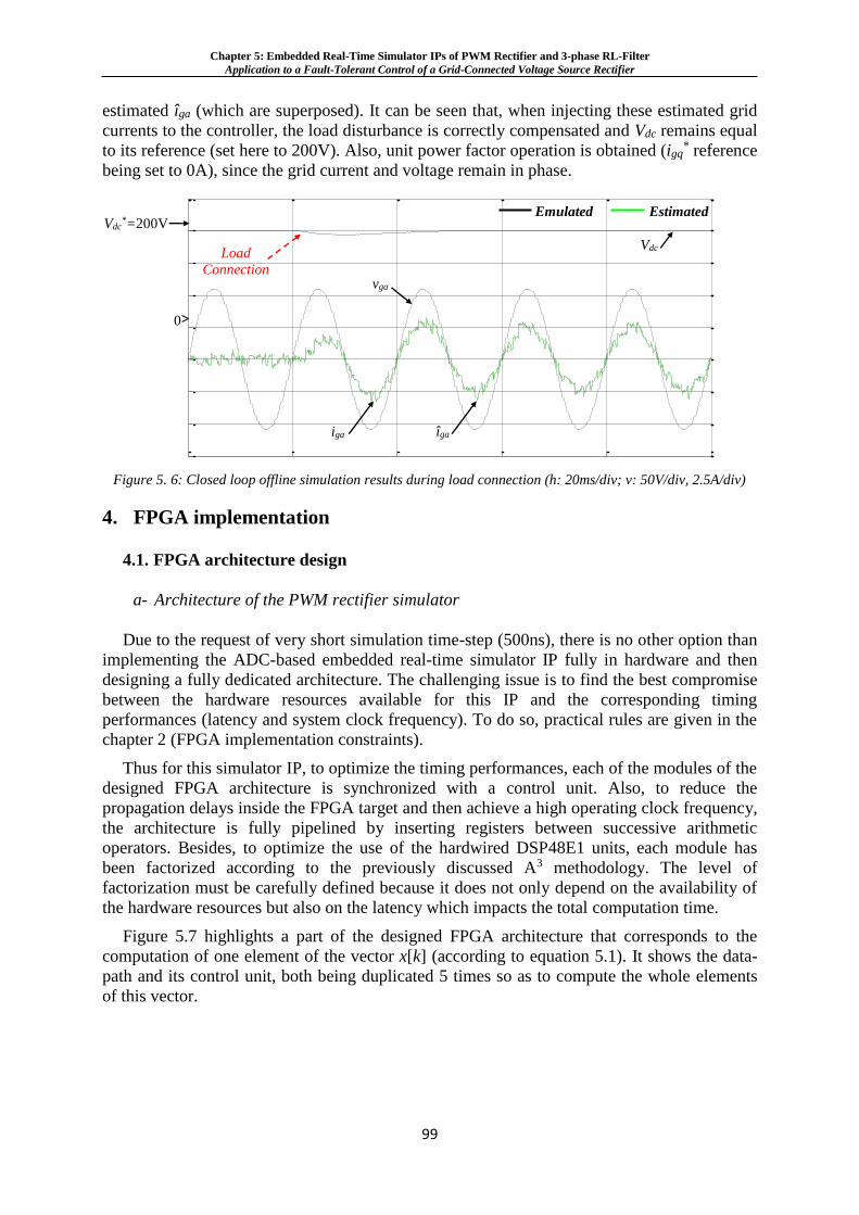
Chapter 5: Embedded Real-Time Simulator IPs of PWM Rectifier and 3-phase RL-Filter
Application to a Fault-Tolerant Control of a Grid-Connected Voltage Source Rectifier
99
estimated îga (which are superposed). It can be seen that, when injecting these estimated grid
currents to the controller, the load disturbance is correctly compensated and Vdc remains equal
to its reference (set here to 200V). Also, unit power factor operation is obtained (igq* reference
being set to 0A), since the grid current and voltage remain in phase.
Figure 5. 6: Closed loop offline simulation results during load connection (h: 20ms/div; v: 50V/div, 2.5A/div)
4. FPGA implementation
4.1. FPGA architecture design
a- Architecture of the PWM rectifier simulator
Due to the request of very short simulation time-step (500ns), there is no other option than
implementing the ADC-based embedded real-time simulator IP fully in hardware and then
designing a fully dedicated architecture. The challenging issue is to find the best compromise
between the hardware resources available for this IP and the corresponding timing
performances (latency and system clock frequency). To do so, practical rules are given in the
chapter 2 (FPGA implementation constraints).
Thus for this simulator IP, to optimize the timing performances, each of the modules of the
designed FPGA architecture is synchronized with a control unit. Also, to reduce the
propagation delays inside the FPGA target and then achieve a high operating clock frequency,
the architecture is fully pipelined by inserting registers between successive arithmetic
operators. Besides, to optimize the use of the hardwired DSP48E1 units, each module has
been factorized according to the previously discussed A3 methodology. The level of
factorization must be carefully defined because it does not only depend on the availability of
the hardware resources but also on the latency which impacts the total computation time.
Figure 5.7 highlights a part of the designed FPGA architecture that corresponds to the
computation of one element of the vector x[k] (according to equation 5.1). It shows the data-
path and its control unit, both being duplicated 5 times so as to compute the whole elements
of this vector.
0.46 0.48 0.5 0.52 0.54 0.56-150
-100
-50
0
50
100
150
200
250Emulated Estimated
Vdc*=200V
Vdc
vga
iga îga
Load
Connection
0
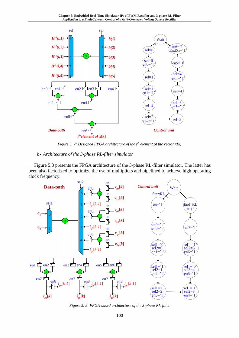
Chapter 5: Embedded Real-Time Simulator IPs of PWM Rectifier and 3-phase RL-Filter
Application to a Fault-Tolerant Control of a Grid-Connected Voltage Source Rectifier
100
Figure 5. 7: Designed FPGA architecture of the ith element of the vector x[k]
b- Architecture of the 3-phase RL-filter simulator
Figure 5.8 presents the FPGA architecture of the 3-phase RL-filter simulator. The latter has
been also factorized to optimize the use of multipliers and pipelined to achieve high operating
clock frequency.
Figure 5. 8: FPGA-based architecture of the 3-phase RL-filter
StartRL
StartXi
Wait
en=’1’
0 0
en0=’1’
sel1=’0’ sel2=0
End_RL
=’1’
en8=’1’
en1=’1’
sel1=’1’ sel2=1 en2=’1’
sel1=’0’ sel2=2 en3=’1’
sel1=’1’ sel2=3 en4=’1’
sel1=’0’ sel2=4 en5=’1’
sel1=’1’ sel2=5 en6=’1’
en7=’1’
0
1
a1
a2
sel1
x
1
2
3
4
5
Data-path
en0
en0
+ -
+ -
en
en
en
en
0
sel2
en0
+ -
en
en
iga
[k-1]
igb
[k-1]
igc
[k-1]
vga
[k]
vLa
[k]
vgb
[k]
vLb
[k]
vgc
[k]
vLc
[k]
+
iga
[k-1]
îga
[k]
en7 en8
en1 en2
+
igb
[k-1]
îgb
[k]
en7 en8
en3 en4
+
igc
[k-1]
îgc
[k]
en7 en8
en5 en6
Control unit
2
1
4
3
sel sel
H-1(i,1)
0
1
2
3
4
H-1(i,2)
H-1(i,3)
H-1(i,4)
H-1(i,5)
b(1)
b(2)
b(3)
b(4)
b(5)
+
en2
en0 en1
+
en4
en2 en3 en4
+
en5
+
en6
Control unit
sel=0
sel=0
en0=’1’
sel=1
EndXi=’1’
Wait
sel=1 en1=’1’
sel=2
sel=2
en2=’1’
en5=’1
’
sel=4
sel=3
en3=’1’ sel=3
en4=’1’
sel=4
en6=’1
’
Data-path
ithelement of x[k] ]
x
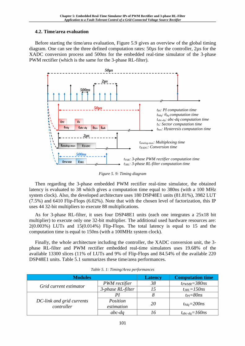
Chapter 5: Embedded Real-Time Simulator IPs of PWM Rectifier and 3-phase RL-Filter
Application to a Fault-Tolerant Control of a Grid-Connected Voltage Source Rectifier
101
4.2. Time/area evaluation
Before starting the time/area evaluation, Figure 5.9 gives an overview of the global timing
diagram. One can see the three defined computation rates: 50µs for the controller, 2µs for the
XADC conversion process and 500ns for the embedded real-time simulator of the 3-phase
PWM rectifier (which is the same for the 3-phase RL-filter).
Figure 5. 9: Timing diagram
Then regarding the 3-phase embedded PWM rectifier real-time simulator, the obtained
latency is evaluated to 38 which gives a computation time equal to 380ns (with a 100 MHz
system clock). Also, the developed architecture uses 180 DSP48E1 units (81.81%), 3982 LUT
(7.5%) and 6410 Flip-Flops (6.02%). Note that with the chosen level of factorization, this IP
uses 44 32-bit multipliers to execute 88 multiplications.
As for 3-phase RL-filter, it uses four DSP48E1 units (each one integrates a 25x18 bit
multiplier) to execute only one 32-bit multiplier. The additional used hardware resources are:
2(0.003%) LUTs and 15(0.014%) Flip-Flops. The total latency is equal to 15 and the
computation time is equal to 150ns (with a 100MHz system clock).
Finally, the whole architecture including the controller, the XADC conversion unit, the 3-
phase RL-filter and PWM rectifier embedded real-time simulators uses 19.68% of the
available 13300 slices (11% of LUTs and 9% of Flip-Flops and 84.54% of the available 220
DSP48E1 units. Table 5.1 summarizes these time/area performances.
Table 5. 1: Timing/Area performances
Modules Latency Computation time
Grid current estimator PWM rectifier 38 tPWMR=380ns
3-phase RL-filter 15 t3RL=150ns
DC-link and grid currents
controller
PI 8 tPI=80ns
Position
estimation 20 tθdq=200ns
abc-dq 16 tabc-dq=160ns
50µs
500ns
2µs
tθdq
tPI
50µs
tS
tabc-dq thys ttab
2µs
tanalog-mux
tXADC
500ns
tPWMR
t3RL
tPI: PI computation time
tθdq: θdq computation time
tabc-dq: abc-dq computation time
tS: Sector computation time
thys: Hysteresis computation time
ttab: Table computation time
tanalog-mux: Multiplexing time
tXADC: Conversion time
tVSR: 3-phase PWM rectifier computation time
t3RL: 3-phase RL-filter computation time
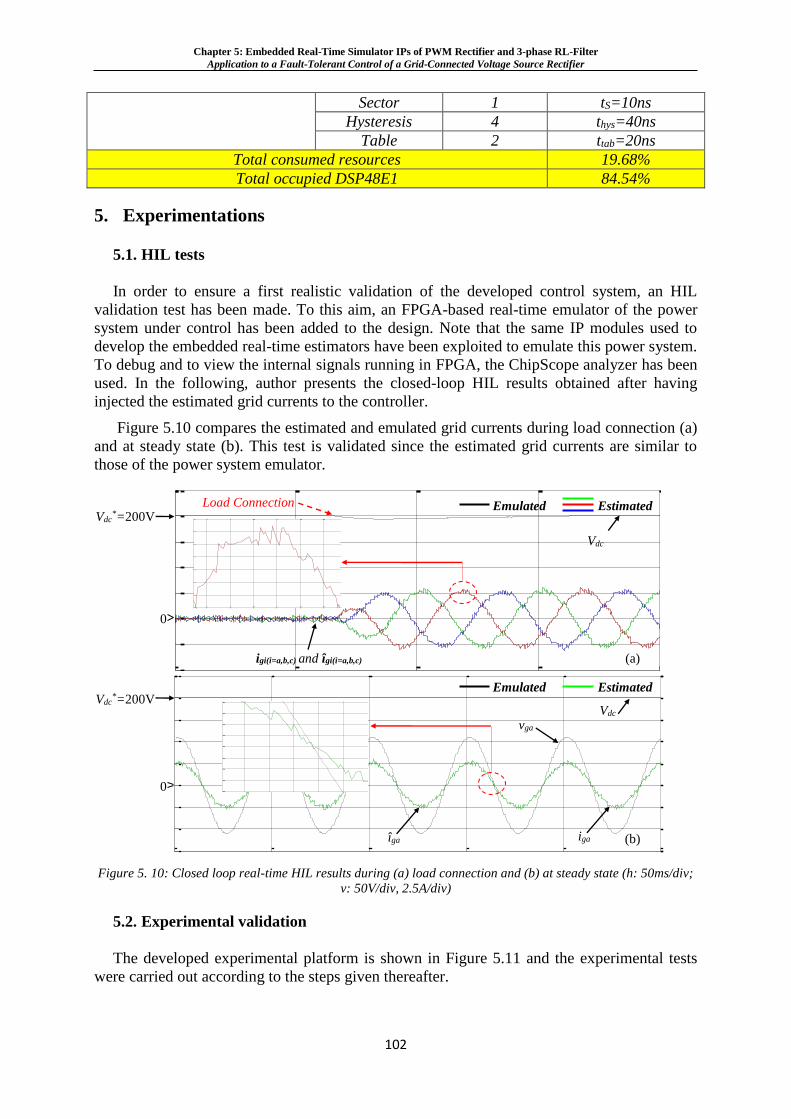
Chapter 5: Embedded Real-Time Simulator IPs of PWM Rectifier and 3-phase RL-Filter
Application to a Fault-Tolerant Control of a Grid-Connected Voltage Source Rectifier
102
Sector 1 tS=10ns
Hysteresis 4 thys=40ns
Table 2 ttab=20ns
Total consumed resources 19.68%
Total occupied DSP48E1 84.54%
5. Experimentations
5.1. HIL tests
In order to ensure a first realistic validation of the developed control system, an HIL
validation test has been made. To this aim, an FPGA-based real-time emulator of the power
system under control has been added to the design. Note that the same IP modules used to
develop the embedded real-time estimators have been exploited to emulate this power system.
To debug and to view the internal signals running in FPGA, the ChipScope analyzer has been
used. In the following, author presents the closed-loop HIL results obtained after having
injected the estimated grid currents to the controller.
Figure 5.10 compares the estimated and emulated grid currents during load connection (a)
and at steady state (b). This test is validated since the estimated grid currents are similar to
those of the power system emulator.
Figure 5. 10: Closed loop real-time HIL results during (a) load connection and (b) at steady state (h: 50ms/div;
v: 50V/div, 2.5A/div)
5.2. Experimental validation
The developed experimental platform is shown in Figure 5.11 and the experimental tests
were carried out according to the steps given thereafter.
0.12 0.14 0.16 0.18 0.2 0.22-100
-50
0
50
100
150
200
250
Emulated Estimated Vdc
*=200V
Vdc
Load Connection
0 0.165 0.166 0.167 0.168 0.169 0.17
25
30
35
40
45
50
55
60
(a) igi(i=a,b,c) and îgi(i=a,b,c)
0.3 0.32 0.34 0.36 0.38 0.4-150
-100
-50
0
50
100
150
200
250
0.163 0.164 0.165 0.166 0.167 0.168
-40
-30
-20
-10
0
10
20
30
40
Vdc
vga
îga iga (b)
Emulated Estimated Vdc
*=200V
0
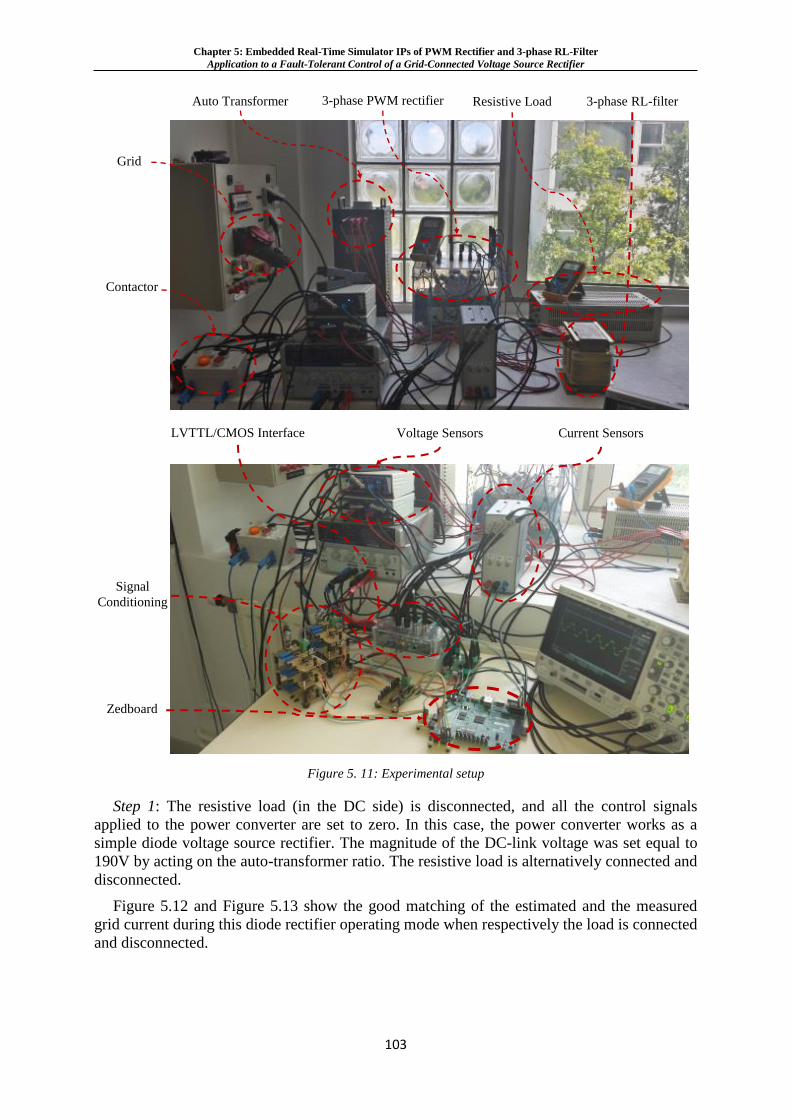
Chapter 5: Embedded Real-Time Simulator IPs of PWM Rectifier and 3-phase RL-Filter
Application to a Fault-Tolerant Control of a Grid-Connected Voltage Source Rectifier
103
Figure 5. 11: Experimental setup
Step 1: The resistive load (in the DC side) is disconnected, and all the control signals
applied to the power converter are set to zero. In this case, the power converter works as a
simple diode voltage source rectifier. The magnitude of the DC-link voltage was set equal to
190V by acting on the auto-transformer ratio. The resistive load is alternatively connected and
disconnected.
Figure 5.12 and Figure 5.13 show the good matching of the estimated and the measured
grid current during this diode rectifier operating mode when respectively the load is connected
and disconnected.
3-phase PWM rectifier Resistive Load 3-phase RL-filter Auto Transformer
Grid
Contactor
Signal
Conditioning
Zedboard
Current Sensors Voltage Sensors LVTTL/CMOS Interface
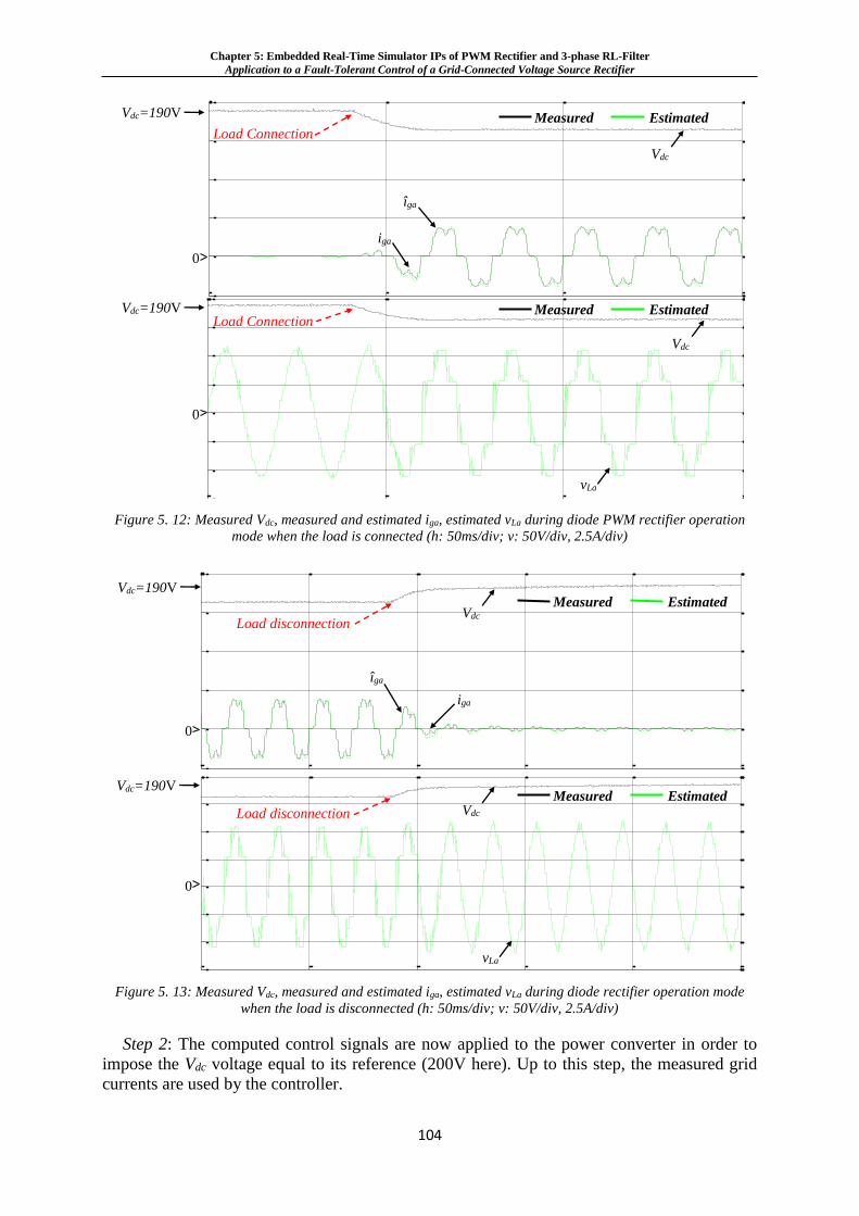
Chapter 5: Embedded Real-Time Simulator IPs of PWM Rectifier and 3-phase RL-Filter
Application to a Fault-Tolerant Control of a Grid-Connected Voltage Source Rectifier
104
Figure 5. 12: Measured Vdc, measured and estimated iga, estimated vLa during diode PWM rectifier operation
mode when the load is connected (h: 50ms/div; v: 50V/div, 2.5A/div)
Figure 5. 13: Measured Vdc, measured and estimated iga, estimated vLa during diode rectifier operation mode
when the load is disconnected (h: 50ms/div; v: 50V/div, 2.5A/div)
Step 2: The computed control signals are now applied to the power converter in order to
impose the Vdc voltage equal to its reference (200V here). Up to this step, the measured grid
currents are used by the controller.
0.05 0.1 0.15 0.2 0.25 0.3-50
0
50
100
150
200
0.05 0.1 0.15 0.2 0.25 0.3-150
-100
-50
0
50
100
150
200
Vdc=190V
0
Vdc=190V
0
Load disconnection
Load disconnection
vLa
Vdc
Vdc
Measured Estimated
Measured Estimated
iga
îga
0.05 0.1 0.15 0.2-50
0
50
100
150
200Vdc=190V
0
Vdc
Measured Estimated Load Connection
iga
îga
0.05 0.1 0.15 0.2-150
-100
-50
0
50
100
150
200Vdc=190V
Load Connection
0
Vdc
vLa
Measured Estimated
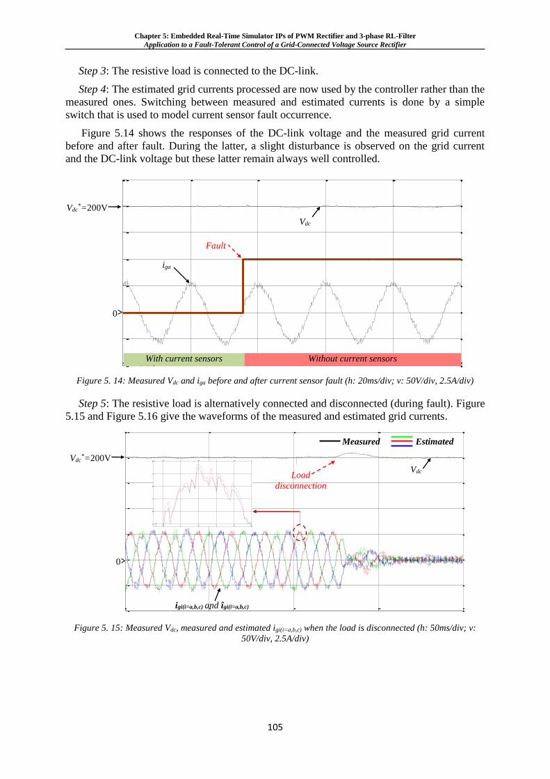
Chapter 5: Embedded Real-Time Simulator IPs of PWM Rectifier and 3-phase RL-Filter
Application to a Fault-Tolerant Control of a Grid-Connected Voltage Source Rectifier
105
Step 3: The resistive load is connected to the DC-link.
Step 4: The estimated grid currents processed are now used by the controller rather than the
measured ones. Switching between measured and estimated currents is done by a simple
switch that is used to model current sensor fault occurrence.
Figure 5.14 shows the responses of the DC-link voltage and the measured grid current
before and after fault. During the latter, a slight disturbance is observed on the grid current
and the DC-link voltage but these latter remain always well controlled.
Figure 5. 14: Measured Vdc and iga before and after current sensor fault (h: 20ms/div; v: 50V/div, 2.5A/div)
Step 5: The resistive load is alternatively connected and disconnected (during fault). Figure
5.15 and Figure 5.16 give the waveforms of the measured and estimated grid currents.
Figure 5. 15: Measured Vdc, measured and estimated igi(i=a,b,c) when the load is disconnected (h: 50ms/div; v:
50V/div, 2.5A/div)
0.05 0.1 0.15 0.2 0.25-100
-50
0
50
100
150
200
250
Vdc*=200V
0
Measured Estimated
Vdc
igi(i=a,b,c) and îgi(i=a,b,c)
0.151 0.152 0.153 0.154 0.155 0.156
35
40
45
50
55
60
Load
disconnection
0.1 0.12 0.14 0.16 0.18 0.2-100
-50
0
50
100
150
200
250
Vdc*=200V
0
Fault
Vdc
iga
Without current sensors
With current sensors
Without current sensors
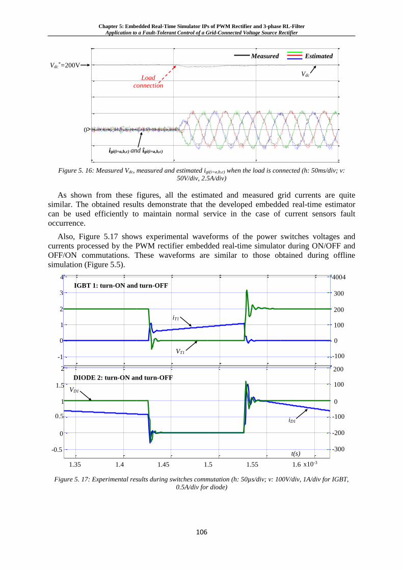
Chapter 5: Embedded Real-Time Simulator IPs of PWM Rectifier and 3-phase RL-Filter
Application to a Fault-Tolerant Control of a Grid-Connected Voltage Source Rectifier
106
Figure 5. 16: Measured Vdc, measured and estimated igi(i=a,b,c) when the load is connected (h: 50ms/div; v:
50V/div, 2.5A/div)
As shown from these figures, all the estimated and measured grid currents are quite
similar. The obtained results demonstrate that the developed embedded real-time estimator
can be used efficiently to maintain normal service in the case of current sensors fault
occurrence.
Also, Figure 5.17 shows experimental waveforms of the power switches voltages and
currents processed by the PWM rectifier embedded real-time simulator during ON/OFF and
OFF/ON commutations. These waveforms are similar to those obtained during offline
simulation (Figure 5.5).
Figure 5. 17: Experimental results during switches commutation (h: 50µs/div; v: 100V/div, 1A/div for IGBT,
0.5A/div for diode)
1.35 1.4 1.45 1.5 1.55 1.6
x 10-3
-1
0
1
2
3
4
1.35 1.4 1.45 1.5 1.55 1.6
x 10-3
-100
0
100
200
300
400
1.35 1.4 1.45 1.5 1.55 1.6
x 10-3
-0.5
0
0.5
1
1.5
2
1.35 1.4 1.45 1.5 1.55 1.6
x 10-3
-300
-200
-100
0
100
200
1.35 x10⁻³ 1.4 1.45 1.5 1.55 1.6
IGBT 1: turn-ON and turn-OFF
DIODE 2: turn-ON and turn-OFF
4004
00
300
200
100
0
-100
200
100
0
-100
-200
-300
VT1
iT1
iD1
VD1
t(s)
4
3
2
1
0
-1
2
1.5
0.5
-0.5
1
0
0.05 0.1 0.15 0.2-100
-50
0
50
100
150
200
250
Vdc*=200V
0
Measured Estimated
Vdc
igi(i=a,b,c) and îgi(i=a,b,c)
Load
connection
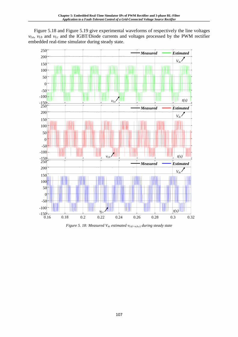
Chapter 5: Embedded Real-Time Simulator IPs of PWM Rectifier and 3-phase RL-Filter
Application to a Fault-Tolerant Control of a Grid-Connected Voltage Source Rectifier
107
Figure 5.18 and Figure 5.19 give experimental waveforms of respectively the line voltages
vLa, vLb and vLc and the IGBT/Diode currents and voltages processed by the PWM rectifier
embedded real-time simulator during steady state.
Figure 5. 18: Measured Vdc estimated vLi(i=a,b,c) during steady state
0.16 0.18 0.2 0.22 0.24 0.26 0.28 0.3 0.32-150
-100
-50
0
50
100
150
200
250
0.16 0.18 0.2 0.22 0.24 0.26 0.28 0.3 0.32-150
-100
-50
0
50
100
150
200
250
0.16 0.18 0.2 0.22 0.24 0.26 0.28 0.3 0.32-150
-100
-50
0
50
100
150
200
250
250
200
150
100
50
0
-50
-100
-150 250
200
150
100
50
0
-50
-100
-150 250
200
150
100
50
0
-50
-100
-150 0.16 0.18 0.2 0.22 0.24 0.26 0.28 0.3 0.32
Measured Estimated
Vdc
Measured Estimated
Vdc
Measured Estimated
Vdc
vLa
vLb
vLc
t(s)
t(s)
t(s)
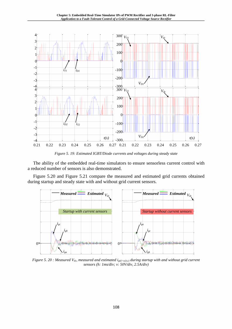
Chapter 5: Embedded Real-Time Simulator IPs of PWM Rectifier and 3-phase RL-Filter
Application to a Fault-Tolerant Control of a Grid-Connected Voltage Source Rectifier
108
Figure 5. 19: Estimated IGBT/Diode currents and voltages during steady state
The ability of the embedded real-time simulators to ensure sensorless current control with
a reduced number of sensors is also demonstrated.
Figure 5.20 and Figure 5.21 compare the measured and estimated grid currents obtained
during startup and steady state with and without grid current sensors.
Figure 5. 20 : Measured Vdc, measured and estimated igi(i=a,b,c) during startup with and without grid current
sensors (h: 1ms/div; v: 50V/div, 2.5A/div)
0.04 0.05 0.06 0.07 0.08 0.09 0.1 0.11-50
0
50
100
150
200
250
igc
igb
iga
0.14 0.15 0.16 0.17 0.18 0.19 0.2 0.21-50
0
50
100
150
200
250
iga
igc
igb
Measured Estimated Vdc Measured Estimated Vdc
Startup with current sensors Startup without current sensors
0 0
0.21 0.22 0.23 0.24 0.25 0.26 0.27-4
-3
-2
-1
0
1
2
3
4
0.21 0.22 0.23 0.24 0.25 0.26 0.27-300
-200
-100
0
100
200
300
0.21 0.22 0.23 0.24 0.25 0.26 0.27-4
-3
-2
-1
0
1
2
3
4
0.21 0.22 0.23 0.24 0.25 0.26 0.27-300
-200
-100
0
100
200
300
4
3
2
1
0
-1
-2
-3
-4 4
3
2
1
0
-1
-2
-3
-4
300
200
0
-100
-200
-300
100
300
200
0
-100
-200
-300
100
0.21 0.22 0.23 0.24 0.25 0.26 0.27 0.21 0.22 0.23 0.24 0.25 0.26 0.27
iT2 iD2
iD1 iT1
Vdc VT1
VD1
Vdc VT2
VD2 t(s) t(s)
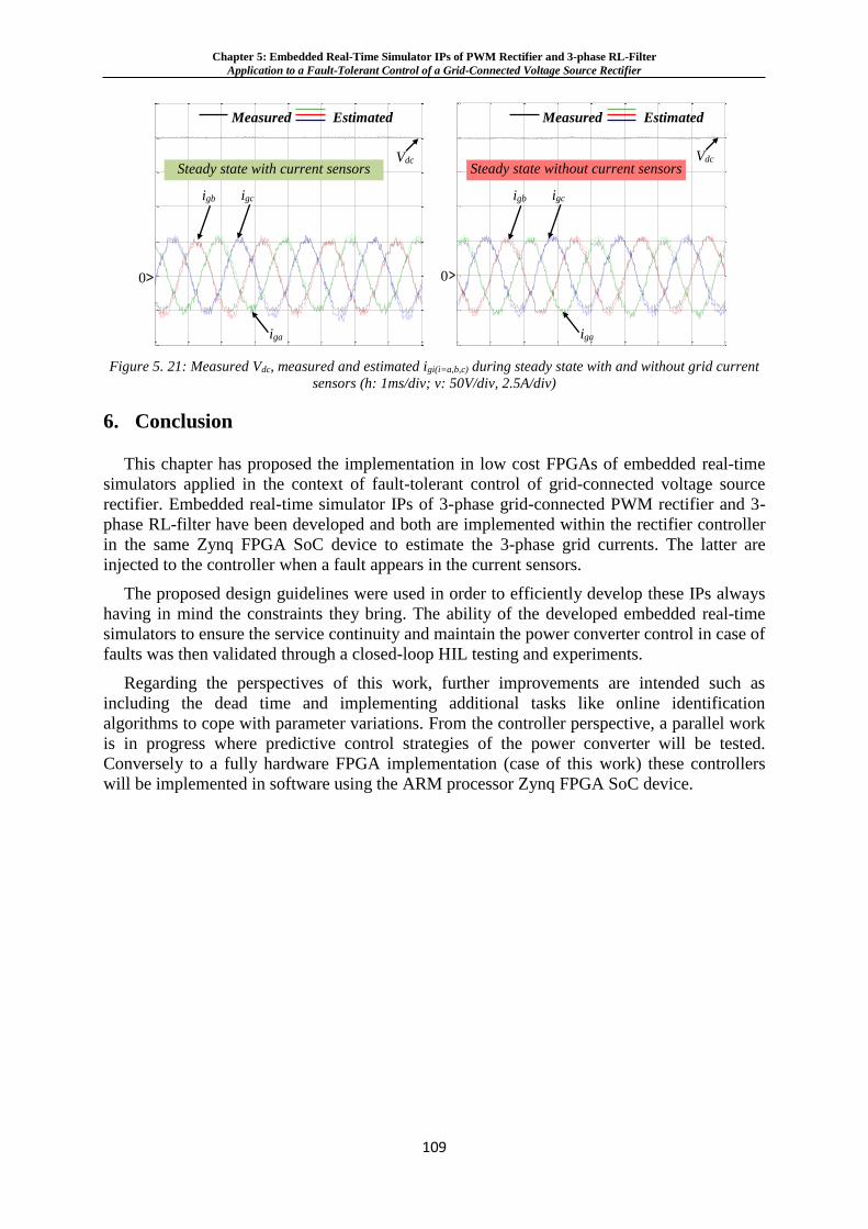
Chapter 5: Embedded Real-Time Simulator IPs of PWM Rectifier and 3-phase RL-Filter
Application to a Fault-Tolerant Control of a Grid-Connected Voltage Source Rectifier
109
Figure 5. 21: Measured Vdc, measured and estimated igi(i=a,b,c) during steady state with and without grid current
sensors (h: 1ms/div; v: 50V/div, 2.5A/div)
6. Conclusion
This chapter has proposed the implementation in low cost FPGAs of embedded real-time
simulators applied in the context of fault-tolerant control of grid-connected voltage source
rectifier. Embedded real-time simulator IPs of 3-phase grid-connected PWM rectifier and 3-
phase RL-filter have been developed and both are implemented within the rectifier controller
in the same Zynq FPGA SoC device to estimate the 3-phase grid currents. The latter are
injected to the controller when a fault appears in the current sensors.
The proposed design guidelines were used in order to efficiently develop these IPs always
having in mind the constraints they bring. The ability of the developed embedded real-time
simulators to ensure the service continuity and maintain the power converter control in case of
faults was then validated through a closed-loop HIL testing and experiments.
Regarding the perspectives of this work, further improvements are intended such as
including the dead time and implementing additional tasks like online identification
algorithms to cope with parameter variations. From the controller perspective, a parallel work
is in progress where predictive control strategies of the power converter will be tested.
Conversely to a fully hardware FPGA implementation (case of this work) these controllers
will be implemented in software using the ARM processor Zynq FPGA SoC device.
0 0.01 0.02 0.03 0.04 0.05 0.06 0.07 0.08-100
-50
0
50
100
150
200
250
0.2 0.21 0.22 0.23 0.24 0.25 0.26 0.27 0.28-100
-50
0
50
100
150
200
250Measured Estimated
Vdc
igc
igb
iga
Measured Estimated
Vdc
igc
igb
iga
Steady state with current sensors Steady state without current sensors
0 0

General conclusion and perspectives
110
General conclusion and perspectives
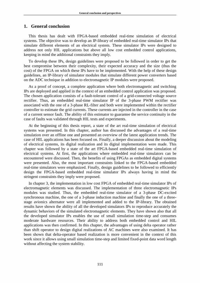
General conclusion and perspectives
111
1. General conclusion
This thesis has dealt with FPGA-based embedded real-time simulation of electrical
systems. The objective was to develop an IP-library of embedded real-time simulator IPs that
simulate different elements of an electrical system. These simulator IPs were designed to
address not only HIL applications but above all low cost embedded control applications,
keeping in mind the additional constraints they imply.
To develop these IPs, design guidelines were proposed to be followed in order to get the
best compromise between their complexity, their expected accuracy and the size (thus the
cost) of the FPGA on which these IPs have to be implemented. With the help of these design
guidelines, an IP-library of simulator modules that simulate different power converters based
on the ADC technique in addition to electromagnetic IP modules were proposed.
As a proof of concept, a complete application where both electromagnetic and switching
IPs are deployed and applied in the context of an embedded control application was proposed.
The chosen application consists of a fault-tolerant control of a grid-connected voltage source
rectifier. Thus, an embedded real-time simulator IP of the 3-phase PWM rectifier was
associated with the one of a 3-phase RL-filter and both were implemented within the rectifier
controller to estimate the grid currents. These currents are injected in the controller in the case
of a current sensor fault. The ability of this estimator to guarantee the service continuity in the
case of faults was validated through HIL tests and experiments.
At the beginning of this thesis report, a state of the art real-time simulation of electrical
systems was presented. In this chapter, author has discussed the advantages of a real-time
simulation over an offline one and presented an overview of the latest application trends. The
case of HIL applications has been focused on. Finally, a deeper discussion about the modeling
of electrical systems, its digital realization and its digital implementation were made. This
chapter was followed by a state of the art FPGA-based embedded real-time simulation of
electrical systems. At first, the applications where embedded real-time simulators can be
encountered were discussed. Then, the benefits of using FPGAs as embedded digital systems
were presented. Also, the most important constraints linked to the FPGA-based embedded
real-time simulators were emphasized. Finally, design guidelines to be followed to efficiently
design the FPGA-based embedded real-time simulator IPs always having in mind the
stringent constraints they imply were proposed.
In chapter 3, the implementation in low cost FPGA of embedded real-time simulator IPs of
electromagnetic elements was discussed. The implementation of three electromagnetic IPs
modules was studied. Thus, the embedded real-time simulator of a 3-phase DC-excited
synchronous machine, the one of a 3-phase induction machine and finally the one of a three-
stage avionics alternator were all implemented and added to the IP-library. The obtained
results have shown the ability of all the developed simulators IPs to reproduce accurately the
dynamic behaviors of the simulated electromagnetic elements. They have shown also that all
the developed simulator IPs enables the use of small simulation time-step and consumes
moderate hardware resources. Their ability to address both embedded control and HIL
applications was then confirmed. In this chapter, the advantages of using delta operator rather
than shift operator to design digital realizations of AC machines were also examined. It has
been shown that delta-operator based realization is more convenient in the context of this
work since it allows using small simulation time-step and limited fixed-point data word length
without affecting the system stability.
General conclusion and perspectives
112
In chapter 4, the FPGA implementation of embedded real-time simulator IPs of static
converters was discussed. The implementation of three IPs was studied: the embedded real-
time simulator of a single phase DC-AC converter, the one of a 3-phase voltage source
inverter and finally the one of a 3-phase diode rectifier were all implemented and added to the
IP-library. The developed real-time simulators were validated in the context of HIL testing.
For each developed simulator, real-time simulation results were provided and compared with
those of offline simulations. The obtained real-time simulation results have clearly
demonstrated the effectiveness of the developed simulator IPs in terms of accuracy and their
ability to be embedded within low-cost FPGA-based controllers using moderate consumed
resources and small time-steps.
In chapter 5, a complete embedded control application was presented. Thus, embedded
real-time simulator IPs of PWM rectifier (switching element) and RL filter (electromagnetic
element) was developed and applied in the context of fault-tolerant control of a grid-
connected voltage source rectifier. They are both embedded within an FPGA-based PWM
rectifier controller and used as a grid current estimator. The ability of this estimator to
guarantee the service continuity and to maintain normal services in the case of current sensor
faults was validated through closed-loop HIL tests and experiments.
2. Perspectives
Regarding the perspectives of this work, further improvements are intended at different
step of the development process of an embedded real-time simulator IP.
When focusing on the algorithm development and particularly on the model selection step,
it is interesting to study the use of more detailed system models that include more nonlinear
phenomena such as saturation and saliency effects. At the digital realization step, an in-depth
analysis of the advantage of using floating-point data format for cost-sensitive embedded real-
time simulation applications is still required.
Additional perspectives related to the FPGA architecture design are to be focused on.
Conversely to a fully hardware FPGA implementation (case of this work), it is also important
to evaluate the value-added of FPGAs for implementing an embedded simulator IP using a
Hardware/Software co-design approach.
From application perspective, it is interesting to evaluate the benefits of using the
developed ADC-based embedded real-time power converter simulator IP for estimation of
conducting and switching losses. As for the developed electromagnetic simulator IPs, it is also
important to study their advantages to be used for online identification of the system
parameters in order to cope with the parameter variations.

Appendices
113
Appendices
Appendix-A: Current-voltage relations of an ADC equivalent circuit
114
Appendix-A: Current-voltage relations of an ADC
equivalent circuit

Appendix-A: Current-voltage relations of an ADC equivalent circuit
115
In this section the extraction of current-voltage relations of an ADC equivalent circuit with
the MNA method is presented. As introduced previously, this method consists in representing
an electrical circuit of n nodes and m independent voltage sources with a matrix equation of
the form:
𝑏 = [
𝑏11𝑏21⋮
𝑏𝑛+𝑚,1
] =
[
ℎ11 ℎ12ℎ21 ℎ22
⋯ ℎ1,𝑛+𝑚⋯ ℎ2,𝑛+𝑚
⋮ ⋮ℎ𝑛+𝑚,1 ℎ𝑛+𝑚,2
⋮ ⋮⋯ ℎ𝑛+𝑚,𝑛+𝑚]
. [
𝑥11𝑥21⋮
𝑥𝑛+𝑚,1
] = 𝐻. 𝑥
Where H is the conductance matrix, x is the vector of unknown variables typically node
voltages and currents through independent voltage sources, b is the vector of known variables
typically voltages sources and combinations, at each voltage node, of independent current
sources.
Extracting current-voltage relations of an ADC equivalent circuit consists then in
determining the conductance matrix H and the x and b vectors. In the following, the steps to
be followed to extract this matrix and vectors are presented and illustrated throughout a
simple example. The chosen ADC equivalent circuit is the one of a half-wave rectifier that
supplies a resistive load (Figure A.1).
Step 1: As illustrated in Figure A.1, the first step consists in selecting a reference node
(usually ground), numbering remaining nodes, labeling currents through each current source
and assigning a name to current through each voltage source.
The studied circuit contains two voltage nodes which are labeled V1 and V2 and one
independent voltage source labeled E. The current through this latter is labeled iE. This circuit
contains also one current source JD. Note that, the number of current sources is dependent on
the way the load is modeled. When this latter is modeled as an external load, load current iL
has to be considered as a current source. Indeed, in this case, the load will not appear in the
matrix H as a conductance (1/R) as explained thereafter but rather in the vector b as a current
source.
Figure A. 1: ADC equivalent circuit of a half-wave rectifier that supplies a resistive load
Step 2: Determine the H matrix, x and b vectors as follows:
The H matrix:
Is (n+m)x(n+m) matrix and contains only known quantities.
The (n)x(n) part of the matrix in the upper left:
Has only passive elements
Each element connected to ground appear only on the diagonal
Elements not connected to ground are both on the diagonal and off-diagonal terms
JD iE
R
G
E
V1 V2
iL
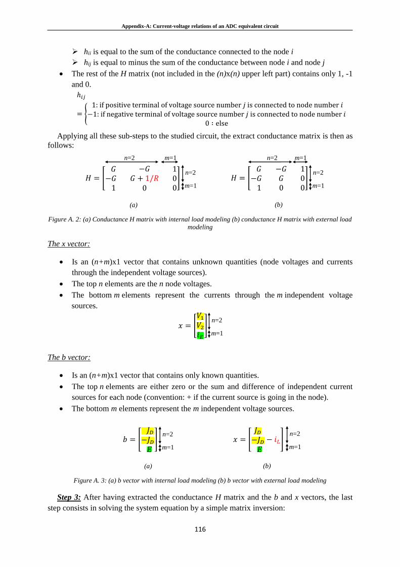
Appendix-A: Current-voltage relations of an ADC equivalent circuit
116
hii is equal to the sum of the conductance connected to the node i
hij is equal to minus the sum of the conductance between node i and node j
The rest of the H matrix (not included in the (n)x(n) upper left part) contains only 1, -1
and 0.
ℎ𝑖𝑗
= 1: if positive terminal of voltage source number 𝑗 is connected to node number 𝑖−1: if negative terminal of voltage source number 𝑗 is connected to node number 𝑖
0 ∶ else
Applying all these sub-steps to the studied circuit, the extract conductance matrix is then as
follows:
Figure A. 2: (a) Conductance H matrix with internal load modeling (b) conductance H matrix with external load
modeling
The x vector:
Is an (n+m)x1 vector that contains unknown quantities (node voltages and currents
through the independent voltage sources).
The top n elements are the n node voltages.
The bottom m elements represent the currents through the m independent voltage
sources.
The b vector:
Is an (n+m)x1 vector that contains only known quantities.
The top n elements are either zero or the sum and difference of independent current
sources for each node (convention: + if the current source is going in the node).
The bottom m elements represent the m independent voltage sources.
Figure A. 3: (a) b vector with internal load modeling (b) b vector with external load modeling
Step 3: After having extracted the conductance H matrix and the b and x vectors, the last
step consists in solving the system equation by a simple matrix inversion:
𝑏 = [ 𝐽𝐷−𝐽𝐷 𝐸
]
n=2
m=1 𝑥 = [
𝐽𝐷−𝐽𝐷 𝐸
− 𝑖𝐿]
n=2
m=1
(a) (b)
𝑥 = [𝑉1𝑉2𝑖𝐸
]
n=2
m=1
𝐻 = [ 𝐺−𝐺 1
−𝐺
𝐺 + 1/𝑅0
100]
n=2
n=2
m=1
m=1 𝐻 = [
𝐺−𝐺 1
−𝐺𝐺0
100]
n=2
n=2
m=1
m=1
(a) (b)
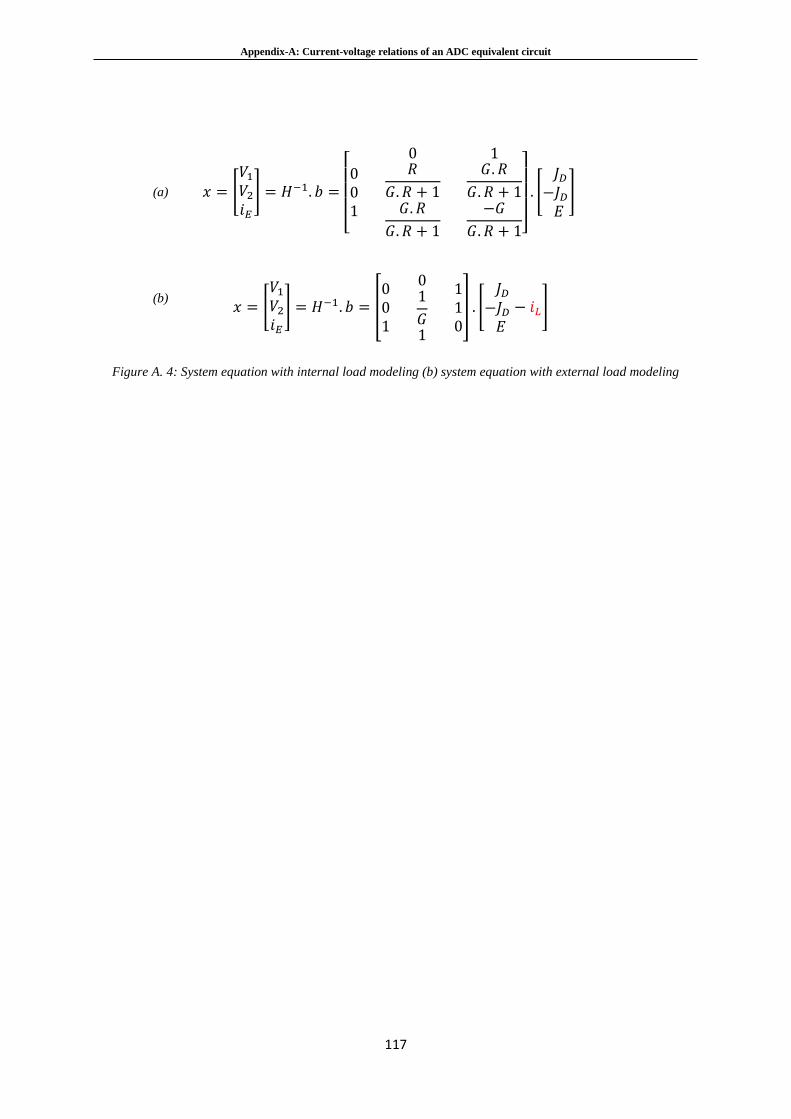
Appendix-A: Current-voltage relations of an ADC equivalent circuit
117
Figure A. 4: System equation with internal load modeling (b) system equation with external load modeling
𝑥 = [𝑉1𝑉2𝑖𝐸
] = 𝐻−1. 𝑏 =
[ 001
0𝑅
𝐺. 𝑅 + 1𝐺. 𝑅
𝐺. 𝑅 + 1
1𝐺. 𝑅
𝐺. 𝑅 + 1−𝐺
𝐺. 𝑅 + 1]
. [ 𝐽𝐷−𝐽𝐷 𝐸
] (a)
(b) 𝑥 = [
𝑉1𝑉2𝑖𝐸
] = 𝐻−1. 𝑏 = [001
01
𝐺1
110] . [
𝐽𝐷−𝐽𝐷 𝐸
− 𝑖𝐿]
Appendix-B: Parameters of the delta-operator based synchronous machine model
118
Appendix-B: Parameters of the delta-operator
based synchronous machine model
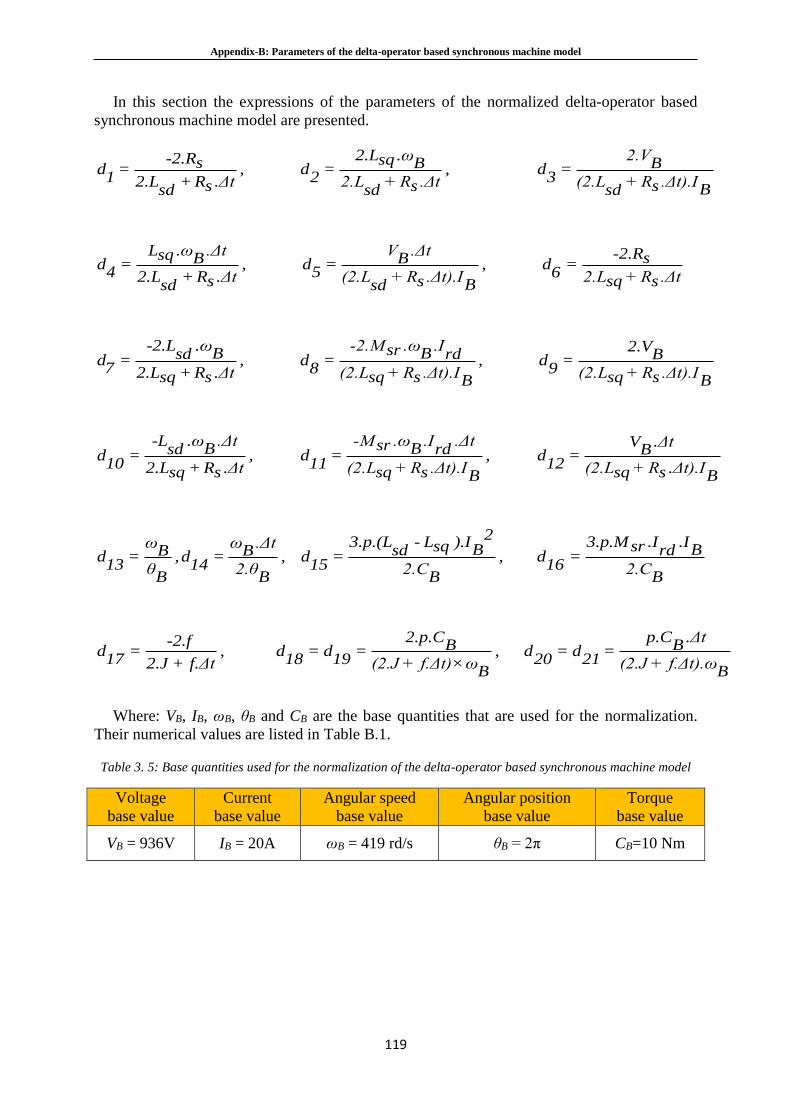
Appendix-B: Parameters of the delta-operator based synchronous machine model
119
In this section the expressions of the parameters of the normalized delta-operator based
synchronous machine model are presented.
2.L .ω 2.V-2.R sqs B Bd = , d = , d =1 2 32.L + R .Δt 2.L +R .Δt (2.L +R .Δt).Is s s Bsd sd sd
L .ω .Δt V .Δt -2.Rsq sB Bd = , d = , d =4 5 62.L + R .Δt (2.L +R .Δt).I 2.L +R .Δts s sq sBsd sd
-2.Ld =7
.ω -2.M .ω .I 2.VsrB Bsd rd B, d = , d =8 92.L + R .Δt (2.L +R .Δt).I (2.L +R .Δt).Isq s sq s sq sB B
-L .ω .Δt -M .ω .I .Δt V .ΔtsrB Bsd rd Bd = , d = , d =10 11 122.L + R .Δt (2.L +R .Δt).I (2.L +Rsq s sq s sq sB
.Δt).IB
23.p.(L - L ).I 3.p.M .I .Iω ω .Δt sq srB Bsd rdB Bd = , d = , d = , d =13 14 15 16θ 2.θ 2.C 2.C
B B B B
2.p.C p.C .Δt-2.f B Bd = , d = d = , d = d =17 18 19 20 212.J + f.Δt (2.J + f.Δt)×ω (2.J + f.Δt).ω
B B
Where: VB, IB, ωB, θB and CB are the base quantities that are used for the normalization.
Their numerical values are listed in Table B.1.
Table 3. 5: Base quantities used for the normalization of the delta-operator based synchronous machine model
Voltage
base value
Current
base value
Angular speed
base value
Angular position
base value
Torque
base value
VB = 936V IB = 20A ωB = 419 rd/s θB = 2π CB=10 Nm
Appendix-C: Poles of the delta-operator based synchronous machine model
120
Appendix-C: Poles of the delta-operator based
synchronous machine model
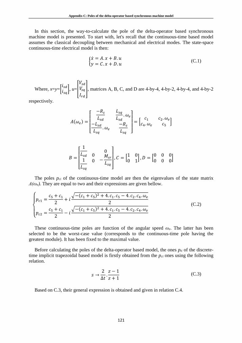
Appendix-C: Poles of the delta-operator based synchronous machine model
121
In this section, the way-to-calculate the pole of the delta-operator based synchronous
machine model is presented. To start with, let's recall that the continuous-time based model
assumes the classical decoupling between mechanical and electrical modes. The state-space
continuous-time electrical model is then:
= 𝐴. 𝑥 + 𝐵. 𝑢𝑦 = 𝐶. 𝑥 + 𝐷. 𝑢
(C.1)
Where, x=y=[𝑖𝑠𝑑𝑖𝑠𝑞], u=[
𝑉𝑠𝑑𝑉𝑠𝑞𝐼𝑟𝑑
], matrices A, B, C, and D are 4-by-4, 4-by-2, 4-by-4, and 4-by-2
respectively.
𝐴(𝜔𝑒) =
[
−𝑅𝑠𝐿𝑠𝑑
−𝐿𝑠𝑑𝐿𝑠𝑞
. 𝜔𝑒
𝐿𝑠𝑞
𝐿𝑠𝑑. 𝜔𝑒
−𝑅𝑠𝐿𝑠𝑞 ]
= [𝑐1
𝑐4. 𝜔𝑒 𝑐2. 𝜔𝑒𝑐5
]
𝐵 =
[ 1
𝐿𝑠𝑑1
𝐿𝑠𝑞
00
0
−𝑀𝑠𝑟
𝐿𝑠𝑞]
, 𝐶 = [10
01] , 𝐷 = [
00
00
00]
The poles pci of the continuous-time model are then the eigenvalues of the state matrix
A(ωe). They are equal to two and their expressions are given bellow.
𝑝𝑐1 =
𝑐5 + 𝑐12
+ 𝑖√−(𝑐1 + 𝑐5)2 + 4. 𝑐1. 𝑐5 − 4. 𝑐2. 𝑐4. 𝜔𝑒
2
𝑝𝑐2 =𝑐5 + 𝑐12
− 𝑖√−(𝑐1 + 𝑐5)2 + 4. 𝑐1. 𝑐5 − 4. 𝑐2. 𝑐4. 𝜔𝑒
2
(C.2)
These continuous-time poles are function of the angular speed ωe. The latter has been
selected to be the worst-case value (corresponds to the continuous-time pole having the
greatest module). It has been fixed to the maximal value.
Before calculating the poles of the delta-operator based model, the ones pti of the discrete-
time implicit trapezoidal based model is firstly obtained from the pci ones using the following
relation.
𝑠 →2
∆𝑡.𝑧 − 1
𝑧 + 1 (C.3)
Based on C.3, their general expression is obtained and given in relation C.4.
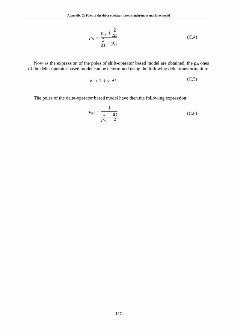
Appendix-C: Poles of the delta-operator based synchronous machine model
122
𝑝𝑡𝑖 =𝑝𝑐𝑖 +
2∆𝑡
2∆𝑡 − 𝑝𝑐𝑖
(C.4)
Now as the expression of the poles of shift-operator based model are obtained, the pdi ones
of the delta-operator based model can be determined using the following delta transformation:
𝑧 → 1 + 𝛾. ∆𝑡 (C.5)
The poles of the delta-operator based model have then the following expression:
𝑝𝑑𝑖 =1
1𝑝𝑐𝑖
−∆𝑡2
(C.6)
Appendix-D: Parameters of the induction machine
123
Appendix-D: Parameters of the induction machine
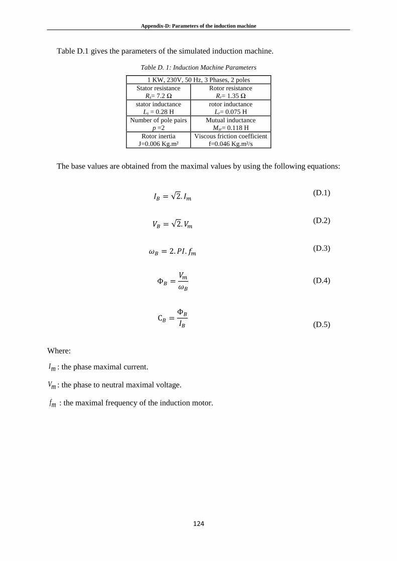
Appendix-D: Parameters of the induction machine
124
Table D.1 gives the parameters of the simulated induction machine.
Table D. 1: Induction Machine Parameters
1 KW, 230V, 50 Hz, 3 Phases, 2 poles
Stator resistance
Rs= 7.2 Ω
Rotor resistance
Rr= 1.35 Ω
stator inductance
Ls = 0.28 H
rotor inductance
Lr= 0.075 H
Number of pole pairs
p =2
Mutual inductance
Msr= 0.118 H
Rotor inertia
J=0.006 Kg.m²
Viscous friction coefficient
f=0.046 Kg.m²/s
The base values are obtained from the maximal values by using the following equations:
𝐼𝐵 = √2. 𝐼𝑚 (D.1)
𝑉𝐵 = √2. 𝑉𝑚 (D.2)
𝜔𝐵 = 2. 𝑃𝐼. 𝑓𝑚 (D.3)
Φ𝐵 =𝑉𝑚𝜔𝐵
(D.4)
C𝐵 =Φ𝐵
𝐼𝐵
(D.5)
Where:
Im : the phase maximal current.
Vm : the phase to neutral maximal voltage.
fm : the maximal frequency of the induction motor.
Appendix-E: Components of the synchronous generator
125
Appendix-E: Components of the three-stage avionics
alternator
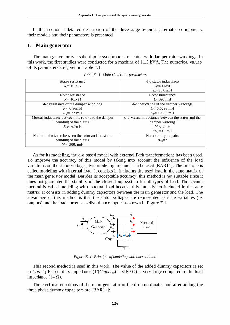
Appendix-E: Components of the synchronous generator
126
In this section a detailed description of the three-stage avionics alternator components,
their models and their parameters is presented.
1. Main generator
The main generator is a salient-pole synchronous machine with damper rotor windings. In
this work, the first studies were conducted for a machine of 11.2 kVA. The numerical values
of its parameters are given in Table E.1.
Table E. 1: Main Generator parameters
Stator resistance
Rs= 10.5 Ω
d-q stator inductance
Ld=63.6mH
Lq=38.6 mH
Rotor resistance
Rf= 10.5 Ω
Rotor inductance
Lf=695 mH
d-q resistance of the damper windings
RD=0.86mH
RQ=0.99mH
d-q inductance of the damper windings
LQ=0.0236 mH
LD=0.0685 mH
Mutual inductance between the rotor and the damper
winding of the d axis
MfD=6.7mH
d-q Mutual inductance between the stator and the
damper winding
MsD=2mH
MsQ=0.9 mH
Mutual inductance between the rotor and the stator
winding of the d axis
Msf =200.5mH
Number of pole pairs
pmg=2
As for its modeling, the d-q based model with external Park transformations has been used.
To improve the accuracy of this model by taking into account the influence of the load
variations on the stator voltages, two modeling methods can be used [BAR11]. The first one is
called modeling with internal load. It consists in including the used load in the state matrix of
the main generator model. Besides its acceptable accuracy, this method is not suitable since it
does not guarantee the stability of the closed-loop system for all types of load. The second
method is called modeling with external load because this latter is not included in the state
matrix. It consists in adding dummy capacitors between the main generator and the load. The
advantage of this method is that the stator voltages are represented as state variables (ie.
outputs) and the load currents as disturbance inputs as shown in Figure E.1.
Figure E. 1: Principle of modeling with internal load
This second method is used in this work. The value of the added dummy capacitors is set
to Cap=1µF so that its impedance (1/(Cap.ωep) = 3180 Ω) is very large compared to the load
impedance (14 Ω).
The electrical equations of the main generator in the d-q coordinates and after adding the
three phase dummy capacitors are [BAR11]:
Main
Generator
n
Cap
iap
ibp
icp
ia1
ib1
ic1
ia2 ib2 ic2
vf
if
Nominal Load
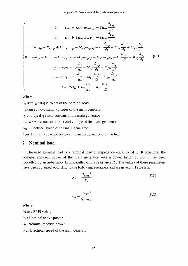
Appendix-E: Components of the synchronous generator
127
𝑖𝑑1 = 𝑖𝑑𝑝 + 𝐶𝑎𝑝. 𝜔𝑒𝑝𝑣𝑞𝑝 − 𝐶𝑎𝑝.
𝑑𝑣𝑑𝑝𝑑𝑡
𝑖𝑞1 = 𝑖𝑞𝑝 + 𝐶𝑎𝑝. 𝜔𝑒𝑝𝑣𝑑𝑝 − 𝐶𝑎𝑝.𝑑𝑣𝑞𝑝𝑑𝑡
0 = −𝑣𝑑𝑝 − 𝑅𝑠𝑖𝑑𝑝 + 𝐿𝑞𝜔𝑒𝑝𝑖𝑞𝑝 −𝑀𝑠𝑄𝜔𝑒𝑝𝑖𝑄 − 𝐿𝑑𝑑𝑖𝑑𝑝𝑑𝑡
+ 𝑀𝑠𝑓
𝑑𝑖𝑓𝑑𝑡+ 𝑀𝑠𝐷
𝑑𝑖𝐷𝑑𝑡
0 = −𝑣𝑞𝑝 − 𝑅𝑠𝑖𝑞𝑝 − 𝐿𝑑𝜔𝑒𝑝𝑖𝑑𝑝 +𝑀𝑠𝑓𝜔𝑒𝑝𝑖𝑓 +𝑀𝑠𝐷𝜔𝑒𝑝𝑖𝐷 − 𝐿𝑞𝑑𝑖𝑞𝑝𝑑𝑡
+ 𝑀𝑠𝑄
𝑑𝑖𝑄𝑑𝑡
𝑣𝑓 = 𝑅𝑓𝑖𝑓 + 𝐿𝑓𝑑𝑖𝑓𝑑𝑡− 𝑀𝑠𝑓
𝑑𝑖𝑑𝑝𝑑𝑡
+ 𝑀𝑓𝐷𝑑𝑖𝐷𝑑𝑡
0 = 𝑅𝐷𝑖𝐷 + 𝐿𝐷𝑑𝑖𝐷𝑑𝑡
+ 𝑀𝑓𝐷𝑑𝑖𝑓𝑑𝑡− 𝑀𝑠𝐷
𝑑𝑖𝑑𝑝𝑑𝑡
0 = 𝑅𝑄𝑖𝑄 + 𝐿𝑄𝑑𝑖𝑄𝑑𝑡
− 𝑀𝑠𝑄
𝑑𝑖𝑑𝑝𝑑𝑡
(E.1)
Where :
id1 and iq1 : d-q currents of the nominal load
vqp and vqp: d-q stator voltages of the main generator
idp and iqp: d-q stator currents of the main generator
if and vf : Excitation current and voltage of the main generator
ωep : Electrical speed of the main generator
Cap: Dummy capacitor between the main generator and the load
2. Nominal load
The used external load is a nominal load of impedance equal to 14 Ω. It consumes the
nominal apparent power of the main generator with a power factor of 0.8. It has been
modelled by an inductance Ln in parallel with a resistance Rn. The values of these parameters
have been obtained according to the following equations and are given in Table E.2:
𝑅𝑛 =𝑈𝑅𝑀𝑆
2
𝑃𝑛
(E.2)
𝐿𝑛 =𝑈𝑅𝑀𝑆
2
𝑄𝑛𝜔ep (E.3)
Where :
URMS : RMS voltage
Pn : Nominal active power
Qn: Nominal reactive power
ωep : Electrical speed of the main generator
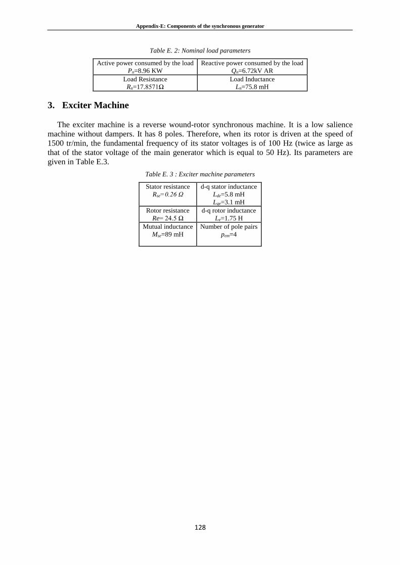
Appendix-E: Components of the synchronous generator
128
Table E. 2: Nominal load parameters
Active power consumed by the load
Pn=8.96 KW
Reactive power consumed by the load
Qn=6.72kV AR
Load Resistance
Rn=17.8571Ω
Load Inductance
Ln=75.8 mH
3. Exciter Machine
The exciter machine is a reverse wound-rotor synchronous machine. It is a low salience
machine without dampers. It has 8 poles. Therefore, when its rotor is driven at the speed of
1500 tr/min, the fundamental frequency of its stator voltages is of 100 Hz (twice as large as
that of the stator voltage of the main generator which is equal to 50 Hz). Its parameters are
given in Table E.3.
Table E. 3 : Exciter machine parameters
Stator resistance
Rse=0.26 Ω
d-q stator inductance
Lde=5.8 mH
Lqe=3.1 mH
Rotor resistance
Re= 24.5 Ω
d-q rotor inductance
Le=1.75 H
Mutual inductance
Mse=89 mH
Number of pole pairs
pem=4
Appendix-F: IPs modules of the 1-phase AC load and P+Resonant current controller
129
Appendix-F: IPs modules of the 1-phase AC load
and P+Resonant current controller
Appendix-F: IPs modules of the 1-phase AC load and P+Resonant current controller
130
To make a complete validation of the ADC-based embedded real-time simulator IP of the
DC-AC converter, this latter has been associated with the ones of a 1-phase AC load and a
P+Resonant based current controller. In this section, these additional IPs are presented and
their time/area performances are summarized.
1. Embedded real-time simulator IP of the 1-phase AC load
This embedded simulator computes the load current iL from the sinusoidal Back EMF
voltage E and the line voltages vLa and vLb processed by the DC-AC simulator.
Figure F. 1: Embedded real-time simulator IP of the 1-phase AC load
The relation F.1 presents the implemented discrete-time equation. The latter is obtained
after the Forward Euler discretization of the RLE circuit.
𝑖𝐿[𝑘] = 𝑎1. ( 𝑣𝐿𝑎[𝑘 − 1] − 𝑣𝐿𝑏[𝑘 − 1] − 𝐸[𝑘]) + 𝑎2. 𝑖𝐿[𝑘 − 1] (F.1)
Where, 𝑎1 =∆𝑡
𝐿 and 𝑎2 = 1 −
∆𝑡.𝑅
𝐿 .
The chosen time-step has been set to 1μs and the chosen fixed-point format is 24Q23 (24
total bit number and 23 bits in the fractional part).
Figure F.2 presents the developed FPGA-based architecture corresponding to the equation
F.1. When using the Xilinx XC7Z020 Zynq device for the implementation of this simulator
IP, the resources consumption is evaluated at 1% of the component slices over 13300 (2
(0.007%) LUTs and 6 (0.01%) Flip-Flops). The computation time is equal to 60ns (with a
100MHz system clock).
Figure F. 2: FPGA-based architecture of the 1-phase AC load
2. AC Load current controller
The goal of this controller consists in regulating the current of the AC load. To this
purpose, the PI regulator can be used. However, this latter is well adopted for the control of
constant quantities (e.g. DC current control) and has less performance for the control of AC
quantities. For a three phase system, the rotating d-q synchronous frame can be used to
en0
en0
en0
vLa[k]
vLb[k]
E[k]
- en1
+
en2 + -
en3 X +
en5 en6 en4
X
iL[k]
a1
a2 en7
en5='1'
End='1'
Reset
Start='1'
en0='1'
en3='1' en6='1'
en1='1' en7='1'
en2='1'
en4='1'
Control Unit Data-Path
Embedded real-time
simulator IP of the 1-
phase AC load
vLa
E
vLb iL
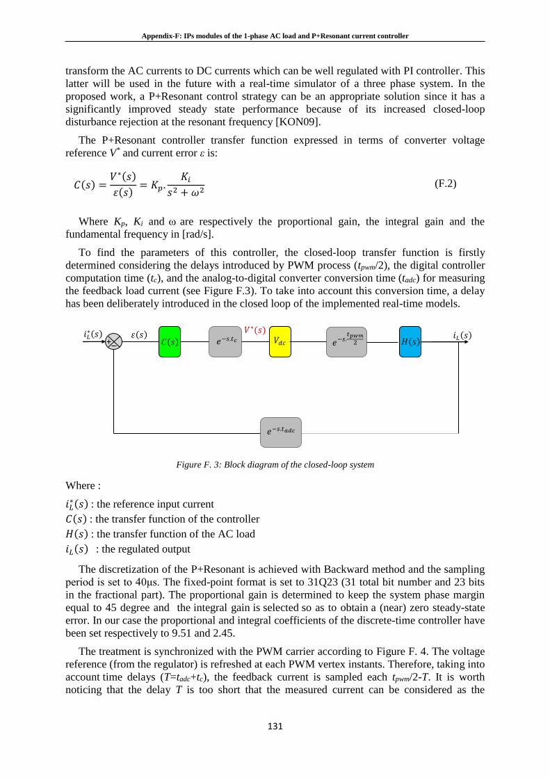
Appendix-F: IPs modules of the 1-phase AC load and P+Resonant current controller
131
transform the AC currents to DC currents which can be well regulated with PI controller. This
latter will be used in the future with a real-time simulator of a three phase system. In the
proposed work, a P+Resonant control strategy can be an appropriate solution since it has a
significantly improved steady state performance because of its increased closed-loop
disturbance rejection at the resonant frequency [KON09].
The P+Resonant controller transfer function expressed in terms of converter voltage
reference V* and current error ε is:
𝐶(𝑠) =𝑉∗(𝑠)
𝜀(𝑠)= 𝐾𝑝.
𝐾𝑖𝑠2 + 𝜔2
(F.2)
Where Kp, Ki and ω are respectively the proportional gain, the integral gain and the
fundamental frequency in [rad/s].
To find the parameters of this controller, the closed-loop transfer function is firstly
determined considering the delays introduced by PWM process (tpwm/2), the digital controller
computation time (tc), and the analog-to-digital converter conversion time (tadc) for measuring
the feedback load current (see Figure F.3). To take into account this conversion time, a delay
has been deliberately introduced in the closed loop of the implemented real-time models.
Figure F. 3: Block diagram of the closed-loop system
Where :
𝑖𝐿∗(𝑠) : the reference input current
𝐶(𝑠) : the transfer function of the controller
𝐻(𝑠) : the transfer function of the AC load
𝑖𝐿(𝑠) : the regulated output
The discretization of the P+Resonant is achieved with Backward method and the sampling
period is set to 40μs. The fixed-point format is set to 31Q23 (31 total bit number and 23 bits
in the fractional part). The proportional gain is determined to keep the system phase margin
equal to 45 degree and the integral gain is selected so as to obtain a (near) zero steady-state
error. In our case the proportional and integral coefficients of the discrete-time controller have
been set respectively to 9.51 and 2.45.
The treatment is synchronized with the PWM carrier according to Figure F. 4. The voltage
reference (from the regulator) is refreshed at each PWM vertex instants. Therefore, taking into
account time delays (T=tadc+tc), the feedback current is sampled each tpwm/2-T. It is worth
noticing that the delay T is too short that the measured current can be considered as the
𝑒−𝑠.𝑡𝑎𝑑𝑐
𝐶(𝑠) 𝑒−𝑠.𝑡𝑐 𝑒−𝑠.𝑡𝑝𝑤𝑚2 𝐻(𝑠) 𝑉𝑑𝑐
𝜀(𝑠) 𝑖𝐿∗(𝑠) 𝑖𝐿(𝑠)
𝑉∗(𝑠)
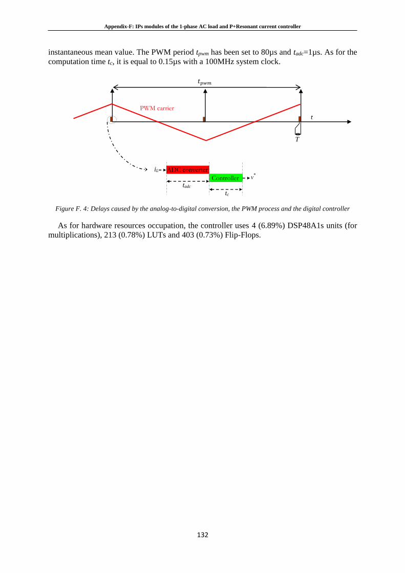
Appendix-F: IPs modules of the 1-phase AC load and P+Resonant current controller
132
instantaneous mean value. The PWM period tpwm has been set to 80µs and tadc=1µs. As for the
computation time tc, it is equal to 0.15µs with a 100MHz system clock.
Figure F. 4: Delays caused by the analog-to-digital conversion, the PWM process and the digital controller
As for hardware resources occupation, the controller uses 4 (6.89%) DSP48A1s units (for
multiplications), 213 (0.78%) LUTs and 403 (0.73%) Flip-Flops.
ADC converter
tadc
T
t
PWM carrier
Controller
tc
iL
V*
𝑡𝑝𝑤𝑚

Bibliography
133
Bibliography
Bibliography
134
[ALT] Altera online documentation available on:http://www.altera.com
[ALI06] D.C. Aliprantis, S.D. Sudhoff, and B.T. Khun,“ A brushless exciter model
incorporating multiple rectifier modes and preisach’s hysteresis theory,” IEEE Transaction
On Energy Conversion, vol. 21, no. 1 :pp. 136–147, 2006.
[ABD09] A. Abdulatif, M. Shaban, “A Matlab / Simulink Based Tool for Power Electronic
Circuits,” in proceeding of world academy of science, engineering and Technology, vol. 49,
pp. 274-278, 2009.
[BEL07] J. Bélanger, V. Lapointe, C. Dufour, L. Schoen, “eMEGAsim: An Open High-
Performance Distributed Real-Time Power Grid Simulator,” in proceedings ICPS conference,
Bangalore, India, 2007.
[BEN10] A. K. Ben Salem, S. B. Othman, S. Ben Saoud,“Field Programmable Gate Array -
Based System-on-Chip for Real-Time Power Process Control,” American Journal of Applied
Sciences, vol.7, no.1, pp 127-139, 2010.
[BEL10] J. Belanger, L. Snider, G. Nanjundaiah,“Today’s Power System Simulation
Challenge: High-performance, Scalable, Upgradable, Affordable COTS-Based Real-Time
Digital Simulators,” in proceeding PEDES conference, New Delh, 2010.
[BEL-10] J. Bélanger, P. Venne, J.-N. Paquin,“The What, Where and Why of Real-Time
Simulation,” OPAL-RT Technologies, www.opal-rt.com/technical-document/what-where-
and-why-real-time-simulation, October 2010.
[BAR11] A. Barakat, S. Tnani, G. Champenois, and E. Mouni, “Monovariable and
multivariable voltage regulator design for a synchronous generator modeled with fixed and
variable loads”. IEEE Transaction On Energy Conversion, vol 26, no. 3, 2011.
[BAH11] I. Bahri, “SW/HW Co-Design methodology for AC Drive applications”, PhD
Thesis, UCP, France-Tunisia, 20011.
[BER12] D.R. Bertenshaw, A.C. Smith, C.W.HO, T. Chan, M. Sasic, “ Detection of stator
core faults in large electrical machines,” IET Power Electronics., vol. 6, no. 6, pp. 295 - 301,
Jul. 2012.
[BAC13] T. Ould Bachir, C. Dufour, J. Bélanger, J. Mahseredjian, J.P. David, "A fully
automated reconfigurable calculation engine dedicated to the real-time simulation of high
switching frequency power electronic circuits," Mathematics and Computers in Simulation,
vol. 91, pp. 167-177, May 2013.
[BAB14] A.S. Babel, E.G.Strangas, “Condition-based monitoring and prognostic health
management of electric machine stator winding insulation,” in proceeding ICEM, Berlin ,
Germany, 2014.
[CHA04] R. Champagne, L. A. Dessaint, H. Fortin-Blanchette and G. Sybille, “Analysis and
Validation of a Real-Time AC Drive Simulator,” IEEE Transactions On Power Electronics,
vol. 19, pp. 336-345, 2004.
[CHA08] L. Charaabi, E.Monmasson, I.Slama-Belkhodja,“FPGA-based real-time emulation
of induction motor using fixed point representation,” in proceeding IECON conference, 2009.
[COR09] P. Cortés, G. Ortiz, J.I. Yuz, J.Rodríguez, S. Vazquez, and L.G. Franquelo,“ Model
Predictive Control of an Inverter With Output LC Filter for UPS Applications ,” IEEE
Transaction On Industrial Electronics , vol. 56, no. 6, June. 2009.
[CAL13] T. Caldognetto, S. Buso, P. Mattavelli, “Digital Controller Development
Methodology Based on Real-Time Simulations with LabVIEW FPGA Hardware-Software
Bibliography
135
Toolset,” Journal of Computational Intelligence and Electronic Systems, vol.17, no.2, pp.110-
117, December, 2013.
[CHE12] Y. Chen, V. Dinavahi, "Digital Hardware Emulation of Universal Machine and
Universal Line Models for Real-Time Electromagnetic Transient Simulation," IEEE
Transactions On Industrial Electronics, vol. 59, no. 2, pp. 1300-1309, February 2012.
[CHE13] Y. Chen and V. Dinavahi,“ Multi-FPGA Digital Hardware Design for Detailed
Large-Scale Real-Time Electromagnetic Transient Simulation of Power Systems,” IEEE IET,
vol. 7, no. 5, pp. 451–463, Juin. 2013.
[DOM69] Dommel, H.W, "Digital computer solution of electromagnetic transients in single-
and multi- phase networks," IEEE Transaction On Power Apparatus and Systems, vol. 88,
no.4, pp. 388–399. 1969.
[DIN00] V. Dinavahi, “Real-time digital simulation of switching power circuits,” Ph.D.
dissertation, Univ. Toronto, Toronto, ON, Canada, 2000.
[DEH05] A. Dehkordi, A. M. Gole, and T. L. Maguire, “Permanent magnet synchronous
machine model for real-time simulation,” in proceeding IPST conference, Montreal, QC,
Canada, June. 2005.
[DUF06] C. Dufour, S. Abourida, J. Bélanger, V. Lapointe, “Real-Time Simulation of
Permanent Magnet Motor Drive on FPGA Chip for High-Bandwidth Controller Tests and
Validation,” in proceedings ISIE conference, Montreal, Que, July 2006.
[DUF07] C. Dufour, J. Bélanger, S. Abourida , V. Lapointe , “FPGA-Based Real-Time
Simulation of Finite-Element Analysis Permanent Magnet Synchronous Machine Drives,” in
proceedings PESC conference, Orlando, FL, 2007.
[DUF07EPE] C. Dufour, J. Bélanger, S. Abourida, V. Lapointe, “Real-Time Simulation of
Finite-Element Analysis Permanent Magnet Synchronous Machine Drives on a FPGA card,”
in proceedings EPE conference, Aalborg, September, 2007.
[DUF07PESC] C. Dufour, J. Belanger, S. Abourida, V. Lapointe, "FPGA-Based Real- Time
Simulation of Finite-Element Analysis Permanent Magnet Synchronous Machine Drives," in
proceeding PESC conference, pp. 944 – 950, 2007.
[DEL11] D. U. C. Delgado and D. R. E. Trejo, “An Observer-based Diagnosis Scheme for
Single and Simultaneous Open-switch Faults in Induction Motor Drives”, IEEE Transaction
on Power Electronics, vol. 58, no. 2, pp. 671 - 679, 2011.
[DAGI11] M. Dagbagi, L. Idkhajine, E. Monmasson, L. Charaabi, and I. Slama-Belkhodja: “FPGA
Implementation of a Synchronous Motor Real-Time Emulator based on Delta Operator”. In
Proceeding ISIE’2011 Conference, pp. 1581-1586, Gdańesk, Poland. 2011.
[DAGS11] M. Dagbagi, L. Charaabi, L. Idkhajine, E. Monmasson, and I. Slama-Belkhodja: “Digital
Implementation using Delta Operator for FPGA based Induction Motor Emulator”. In Proceeding,
SSD'2011 Conference, pp. 1-6, Sousse, Tunisia. 2011.
[DAG12] M. Dagbagi, L. Idkhajine, E. Monmasson, and I. Slama-Belkhodja: “FPGA
Implementation of Power Electronic Converter Real-Time Model”. In Proceeding SPEEDAM’2012
Conference, pp. 658-663, Sorrento, Italy.
[DEB12] M. Debbou, M. Abdellatif, M. Pietrzak-David, “Analytical redundancy for service
continuity of Doubly Fed Induction Machine speed drive,” in proceeding ICEM, pp. 858-864,
Marseille, France, September .2012.
Bibliography
136
[DAGS12] M. Dagbagi, L. Idkhajine, E. Monmasson, and I. Slama-Belkhodja: “FPGA
Implementation of Power Electronic Converter Real-Time Model”. In Proceeding SPEEDAM’2012
Conference, pp. 658-663, Sorrento, Italy. 2012.
[DAGP13] M. Dagbagi, L. Idkhajine, M.Tientcheu-Yamdeu, E. Monmasson, and I. Slama-
Belkhodja: "FPGA-based Brushless Synchronous Generator Real-Time Emulator Prototype for
Digital Controllers Testing". In Proceeding PCIM’2013 Conference, pp. 1707-1714, Nuremberg,
Germany. 2013.
[DAGI13] M. Dagbagi, A. Hemdani, L. Idkhajine, M. W. Naouar, E. Monmasson, and I. Slama-
Belkhodja: "FPGA-based Real-Time Hardware-In-the-Loop validation of a 3-phase PWM Rectifier
controller". In Proceeding IECON’2013 Conference, pp. 5374 - 5379, Vienna, Austria. 2013.
[DAGJ13] M. Dagbagi: "Implantation sur une cible FPGA d'un simulateur temps réel d'un redresseur
MLI triphasé". In Proceeding SEEDS-JCGE'2013 Conference, Saint Nazaire, France. 2013.
[DAGP15] M. Dagbagi, L. Idkhajine, E. Monmasson: " Simulation temps-réel des systèmes
électriques – Implantation sur cible FPGA du simulateur temps réel d'un redresseur MLI
triphasé". Revue 3EI, n° 80, pp. 36-42, Avril 2015.
[DAGI15] A. Hemdani, M. Dagbagi, M. W. Naouar, L. Idkhajine, I. Slama-Belkhodja, and E.
Monmasson: "Indirect Sliding Mode Power Control for Three Phase Grid Connected Power
Converter". IET Power Electronics Journal, vol. 8, No. 6, pp. 977-985, June 2015.
[DAGT15] M. Dagbagi, A. Hemdani, L. Idkhajine, M. W. Naouar, E. Monmasson, and I. Slama-
Belkhodja: "ADC-based Embedded Real-Time Simulator of a Power Converter Implemented in a
Low Cost FPGA: Application to a Fault-Tolerant Control of a Grid-Connected Voltage Source
Rectifier". IEEE Transaction on Industrial Electronics. (Accepted).
[GOL84] A. M. Gole, R. W. Menzies, H. M. Turanli, and D. A.Woodford, "Improved
Interfacing of Electrical Machine Models to Electromagnetic Transients Programs," IEEE
Transaction On Power Apparatus and Systems, vol. PAS-103, no. 9, pp. 2446-2451,1984.
[GAN93] Gang. L, Gevers. M,“Comparative Study of Finite Wordlength Effects in Shift and
Delta Operator Parameterizations,” IEEE Transaction On Automatic Control, vol. 38, no. 5,
pp.803-807, 1993.
[GAN93_2] Gang. L, Gevers. M,“Roundoff noise minimization using delta-operator
realizations,” IEEE Transaction On Signal Processing, vol. 41, no. 2, pp.629-637, 1993.
[GRA99] T. Grandpierre, C Lavrenne and Y. Sorel, “Optimized rapid prototyping for real-
time embedded heterogeneous multiprocessor,” in Proc. CODES’99 7th International
Workshop on Hardware/ Software Co-Design Conf., pp. 74-78.
[GON14] O. Goni, A. Sanchez, E. Todorovich, A. de Castro, “Resolution analysis of
switching converter models for hardware-in-the-loop”, IEEE Transaction on Industrial
Informatics, vol. 10, no. 1, pp. 1162-1170, Mai, 2014.
[HUI94] S. Y. R. Hui and S. Morrall, “Generalised Associated Discrete Circuit Model for
Switching Devices,” in proceeding IEE Science, Measurement and Technology, vol. 141, no.
1, pp. 57–64, 1994.
[HAS14] A. Hasanzadeh, C.S. Edrington, N. Stroupe, T. Bevis, "Real-Time Emulation of a
High-Speed Microturbine Permanent-Magnet Synchronous Generator Using Multiplatform
Hardware-in-the- Loop Realization," IEEE Transactions On Industrial Electronics, vol. 61,
no. 6, pp.3109-3118, June 2014.
Bibliography
137
[HEM15] A. Hemdani , “ Intégration d’une charge intelligente à base d’un redresseur MLI
triphasé dans un micro-réseau”, PhD Thesis, ENIT, Tunisia, 2015.
[IDK10] L.Idkhajine,“ Fully FPGA-based Sensorless Control for Synchronous AC Drive
using an Extended Kalman Filter,”PhD Thesis, Cergy Pontoise University, 2010.
[JIN97] H. Jin, "Behavior-mode Simulation of Power Electronic Circuits," IEEE Transaction
On Power Electronics, vol. 12, no. 3, pp. 443-452, 1997.
[JIA11] H. Jiabing, S. Lei, H. Yikang and Z. Q. Zhu “Direct active and reactive power
regulation of grid connected DC/AC converters using sliding mode control approach,” IEEE
Transactions on Power Electronics, vol.26, pp. 210-222, January 2011.
[JIA14] L. Jiadai, V. Dinavahi, "A Real-Time Nonlinear Hysteretic Power Transformer
Transient Model on FPGA," IEEE Transaction On Industrial Electronics, vol. 61, no. 7,
pp.3587-3597, Jul.2014.
[JIM15] O. Jimenez et al., “Implementation of an FPGA-based on-line hardware-in the-loop
emulator using high-level synthesis tools for resonant power converters applied to induction
heating appliances”, IEEE Transaction on Industrial Electronics, vol. 62, no. 4, pp. 2206-
2214, April, 2015.
[KAU97] Kauraniemi. J, Laakso. T. I, “Roundoff noise analysis of modified Delta operator
direct form structures,” IEEE Transaction On Circuits and Systems, vol. 4, pp.2365-2368,
1997.
[KAR09] S. Karimi,P.Poure, andS.Saadate, “Fast power switch failure detection for fault
tolerant voltage source inverters using FPGA,” IET Power Electronics, vol. 2, no. 4, pp. 346–
354, Jul. 2009.
[KON09] W.Y.Kong, D. G. Holmes, B. P. McGrath, “Improved Stationary Frame AC Current
Regulation using Feed forward Compensation of the Load EMF,” in proceeding APEC2009
conference, Washington, DC, 2009.
[KIF11] A. Kiffe, S. Geng, T. Schulte, J. Maas, "Real-Time Simulation of Power Electronic
Circuits based on Discrete Averaging Method," in proceeding IECON conference,
Melbourne, VIC, 2011.
[KAM13] M. Kaminski, T. Orlowska-Kowalska, "FPGA Implementation of ADALINE-
Based Speed Controller in a Two-Mass System," IEEE Transactions On Industrial
Informatics, vol. 9, no. 3, pp. 1301-1311, August 2013.
[LI93] G. Li, M. Gevers, " Roundoff Noise Minimisation Using Delta Operator Realisations,"
IEEE Transaction On Signal Processing, vol. 42, no, February 1993.
[LI20] LI. G, Wu. J, Chen. S, Chu. J, “Optimal finite precision state- Estimate feecback
controller realizations of discretre-time systems,” IEEE Transaction On Automatic Control,
vol. 45, no. 8, pp.1550-1554, 2000.
[LUC11] O. Lucía, I. Urriza, L.A. Barragán, D. Navarro, O. Jiménez, J.M. Burdío, "Real-
Time FPGA-Based Hardware-in-the-Loop Simulation Test Bench Applied to Multiple-Output
Power Converters," IEEE Transactions On Industry Applications, vol. 47, no. 2, pp. 853-860,
March-April 2011.
[MAR89] J. R. Marti and J. Lin, "Suppression of numerical oscillations in the EMTP," IEEE
Trans. Power Syst., vol. 9, no. 1, pp. 71–72, Feb. 1989.
[MID90] H. Middleton and G. C. Goodwin, Digital Control and Estimation: A Unified
Approach. Englewood Cliffs, NJ: Prentice- Hall, 1990.
Bibliography
138
[MAR97] J. R. Marti and K. W. Louie, “A phase-domain synchronous generator model
including saturation effects,” IEEE Transaction On Power Systems, vol. 12, no. 1, pp. 222–
229, Feb. 1997.
[MAR06] C.C. Marouchos," The Switching Function: Analysis of Power Electronic Circuits,"
IET. 2006. 297 pages.
[MAT09] M. Matar, R. Iravani, “FPGA implementation of a modified two- layer network
equivalent for real-time simulation of electromagnetic transients,” in proceeding IPST
conference, Kyoto, Japan, Jun. 2009.
[MAT10] M. Matar, R. Iravani, "FPGA Implementation of the Power Electronic Converter
Model for Real-Time Simulation of Electromagnetic Transients," IEEE Transaction On
Power Delivery, vol. 25, no. 2, pp.852-860, April 2010.
[MEN10] P.M.Menghal, A. Jaya Laxmi, “Real Time Control of Electrical Machine Drives: A
Review,” in proceeding ICPCES conference, Allahabad, 2010.
[MAJ11] D. Majstorovic, I. Celanovic, N.D. Teslic, N. Celanovic, V.A. Katic, "Ultralow-
Latency Hardware-in-the-Loop Platform for Rapid Validation of Power Electronics Designs,"
IEEE Transactions On Industrial Electronics , vol. 58, no. 10, pp. 4708-4716, October 2011.
[MAT11] M. Matar, R. Iravani “Massively Parallel Implementation of AC Machine Models
for FPGA-Based Real-Time Simulation of Electromagnetic Transients”, IEEE Transaction
On Power Delivery, vol. 26, no. 2, April 2011.
[MYA11] A. Myaing, V. Dinavahi, "FPGA-Based Real-Time Emulation of Power Electronic
Systems With Detailed Representation of Device Characteristics," IEEE Transaction On
Industrial Electronics, vol. 58, no. 1, pp. 358- 368, January 2011.
[MAT11IPST] M. Matar, M. Saeedifard, A. Etemadi, R. Iravani, “An FPGA-Based
Hardware-in-the-Loop Simulator for Multilevel Converter Systems,” in proceeding IPST
conference, in Delft, The Netherlands, June, 2011.
[MON11] E. Monmasson, L. Idkhajine, M. N. Cirstea, I. Bahri, A.Tisan, M. W. Naouar,
"FPGAs in industrial control applications," IEEE Transaction On Industrial Informatics,
vol.7, no.2, pp.224-243, May 2011.
[MON12] E. Monmasson, I.Bahri, L. Idkhajine, A. Maalouf, W. M. Naouar,“ Recent
Advancements in FPGA-based controllers for AC Drives Applications,” in proceeding
OPTIM conference, Brasov, May, 2012.
[MAR12] S. Mariethoz, A. Domahidi, M. Morari,“High-bandwidth explicit model predictive
control of electrical drives,” IEEE Transactions on Industry Applications, vol. 48, no. 6,
pp.1980-1992, 2012.
[MAT13] M. Matar, R. Iravani, “The Reconfigurable-Hardware Real-Time and Faster-Than-
Real-Time Simulator for the Analysis of Electromagnetic Transients in Power Systems,”
IEEE Transaction On Power Delivery, vol. 28, n° 2, pp. 619-627, April 2013.
[NAO07] M. W. Naouar, E. Monmasson, A. Naassani, I. Slama-Belkhodja, N. Patin, “FPGA-
based current controllers for AC machine drives– A review,” IEEE Transactions On
Industrial Electronics, vol. 54, no. 4, pp. 1907-1925, August 2007.
[NAO07P] M. W. Naouar, “Commande numérique à base de composants FPGA d’une
machine synchrone”, PhD Thesis, UCP-ENIT, France-Tunisia, 2007.
Bibliography
139
[NOD11] T. Noda, S. Filizadeh, A. R. Chevrefils, M. Matar, R. Iravani, C. Dufour, J.
Belanger, M. O. Faruque,“ Interfacing Issues in Real-Time Digital Simulators ,” IEEE
Transaction On Power Delivery, vol . 26, no. 2, April 2011.
[NUS14] P. Nussbaumer, M.A. Vogelsberger, T. Wolbank, “Induction Machine Insulation
Health State Monitoring Based on Online Switching Transient Exploitation,” IEEE
Transaction On Industrial Electronics , vol. pp, no. 29, October, 2014.
[OPA] OPAL-RT website on:http://www.opal-rt.com
[ORI06] R. Orizondo, R. Alves, “UPFC Simulation and Control Using the ATP/EMTP and
MATLAB/Simulink Programs,” in proceeding PES conference, Latin America, Venezuela,
2006.
[OUL13] T. Ould Bachir, C. Dufour, J. Bélanger, J. Mahseredjian, J.P. David, "A fully
automated reconfigurable calculation engine dedicated to the real-time simulation of high
switching frequency power electronic circuits," Mathematics and Computers in Simulation,
vol. 91, pp. 167-177, May 2013.
[PEJ94] P. Pejovic and D. Maksimovic, "A Method for Fast Time-Domain Simulation of
Networks with Switches," IEEE Transactions on Power Electronics, vol. 9, no. 4, pp. 449–
456, 1994.
[PEL12] P. Peltoniemi, P. Nuutinen, J. Pyrhonen , “Observer-Based Output Voltage Control
for DC Power Distribution Purposes,” IEEE Transactions On Power Electronics, vol. 28,
no.4, pp.1914-1926, 2012.
[QUN11] AN Quntao, SUN Lizhi, ZHAO Ke, “Switching function model-based fast-
diagnostic method of open-switch faults in inverters without sensors”, IEEE Transaction on
Power Electronics, vol. 26, no. 1, pp. 119- 126, 2011.
[QUE12] L. Quéval, H. Ohsaki, “Study on the implementation of the phase-domain model for
rotating electrical machines,” 15th International Conference on Electrical Machines and
Systems (ICEMS2012), Sapporo, Japan, October 2012.
[RTD] RTDS website on:http://www.rtds.com
[RIC02] F. Ricci and H. Le-Huy, “An FPGA-based rapid prototyping platform for variable-
speed drives,” in Proc. IEEE IECON’02 Conf., 2002, pp. 1156–1161.
[RAJ05] A.D. Rajapakse, A.M. Gole, P.L. Wilson, “Electromagnetic Transients Simulation
Models for Accurate Representation of Switching Losses and Thermal Performance in Power
Electronic Systems,” IEEE Transaction On Power Delivery, vol. 20, n° 1, pp. 319-327,
January 2005.
[RAK11] M. Rakotozafy, P. Poure, S. Saadate, C. Bordas, L. Leclere, " Real-time digital
simulation of power electronics systems with Neutral Point Piloted multilevel inverter using
FPGA, " Electric Power Systems Research, vol. 81, no. 2, pp. 687–698, 2011.
[REZ13] Mohammad Reza, “An Improved State Space Average Model of Buck DC-DC
Converter with all of the System Uncertainties”, in International Journal on Electrical
Engineering and Informatics, vol 5, no 1, March 2013.
[RAJ13] S. Rajendran, U. Govindarajan, S. Senthilvadivelu, S. B. Uandai, “Intelligent
sensor fault-tolerant control for variable speed wind electrical systems ,” IET Power
Electronics, vol. 6, no. 7, pp. 1308 - 1319, August. 2013.
[RAK14] A.M. Rakotozafy,“ Simulation Temps réel de dispositifs électrotrchniques ,”PhD
Thesis, Lorraine University, 2014.
Bibliography
140
[SAL94] L. Salazar, G. Joos, " PSPICE Simulation of Three-Phase Inverters by Means of
Switching Functions, " IEEE Transaction On Power Electronics, vol. 9, no. 1, pp. 35-42,
1994.
[SIM09] SimPowerSystems, User's Guide, Version 5, The MathWorks Inc., 2009.
[SEU12] T. C. Seung, W. Qiuwei , A.H Nielsen, J. Ostergaard, I.K Park , “Real-Time
Hardware-in-the-Loop (HIL) Testing for Power Electronics Controllers,” in proceeding
APPEEC conference, Shanghai, March 2012.
[SAN12] A. Sanchez, A. de Castro, and J. Garrido, "A comparison of simulation and
hardware-in-the- loop alternatives for digital control of power converters, " IEEE Transaction
On Industrial Informatics, vol. 8, no. 3, pp. 491 –500, Aug. 2012.
[SHA13] M. Shahbazi, P. Poure, S. Saadate, ; M.R. Zolghadri "FPGA Based Fast Detection
With Reduced Sensor Count for a Fault- Tolerant Three-Phase Converter," IEEE
Transactions On Industrial Informatics, vol. 9, no. 3, pp.1343-1350, August 2013.
[SHAH13] M. Shahbazi, P. Poure, S. Saadate, M.R. Zolghadri, "FPGA Based
Reconfigurable Control for Fault-Tolerant Back-to-Back Converter Without Redundancy,"
IEEE Transactions On Industrial Electronics , vol. 60, no. 8, pp. 3360-3371, August 2013.
[SUT13] T. Sutikno, N.R.N. Idris, A. Jidin, M.N. Cirstea, "An Improved FPGA
Implementation of Direct Torque Control for Induction Machines," IEEE Transactions On
Industrial Informatics, vol. 9, no. 3, pp. 1280-1290, August 2013.
[SON14] Y. Song, L. Chen, Y. Chen, and S. Huang, "A General Parameter Configuration
Algorithm for Associate Discrete Circuit Switch Model," In Proceedings POWERCON'2014
Conference, Chengdu, China.
[SCH14] A. Schmitt, J. Richter, U. Jurkewitz, M. Braun, “FPGA-based real time simulation
of nonlinear permanent magnet synchronous machines for power hardware-in-the-loop
emulation systems”, in proceeding IECON '14 conference, 2014.
[WAN10] L. Wang et al., “Methods of interfacing rotating machine models in transient
simulation programs,” IEEE Transaction On Power Delivery, vol. 25, no. 2, pp. 891-903,
Apr. 2010.
[XIL] Xilinx online documentation available on:http://www.xilinx.com
[YIN13] Ying Zhu, Ming Cheng, Wei Hua, Bangfu Zhang,“ Sensorless Control Strategy of
Electrical Variable Transmission Machines for Wind Energy Conversion Systems,” IEEE
Transactions On Magnetics, vol. 49, no.7, pp. 3383 - 3386, 2013.
[ZHA05] T. Zhao, Q. Wang, “Application of MATLAB/SIMULINK and PSPICE Simulation
in Teaching Power Electronics and Electric Drive System,” in proceedings of the Eighth
International Conference on Electrical Machines and Systems, pp 2037–2041, Nanjing,
China. 2005.
[ZOE14] C. Zoeller, M. Vogelsberger, P. Nussbaumer, T. Wolbank , “Insulation monitoring
of three phase inverter-fed AC machines based on two current sensors only,” in proceeding
ICEM, Berlin , Germany, 2014.