Embed Size (px)
Citation preview
Hardware attacks: theory and experimental state-of-the-art of laser fault injection attacks
Journées Nationales 2018 Pré-GDR Sécurité Informatique
Sécurité des systèmes matériels
Département Systèmes et Architectures Sécurisées
Mines Saint-Etienne, Centre de Microélectronique de Provence
13541 Gardanne FRANCE
Jean-Max Dutertre, 30 mai 2018, Jussieu
Position of the problem
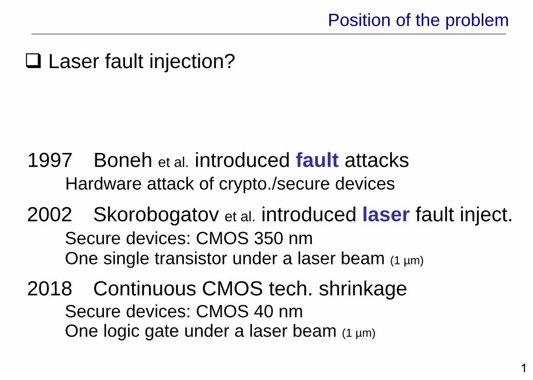
Laser fault injection?
1997 Boneh et al. introduced fault attacksHardware attack of crypto./secure devices
2002 Skorobogatov et al. introduced laser fault inject.Secure devices: CMOS 350 nmOne single transistor under a laser beam (1 µm)
2018 Continuous CMOS tech. shrinkageSecure devices: CMOS 40 nmOne logic gate under a laser beam (1 µm)
1
Position of the problem
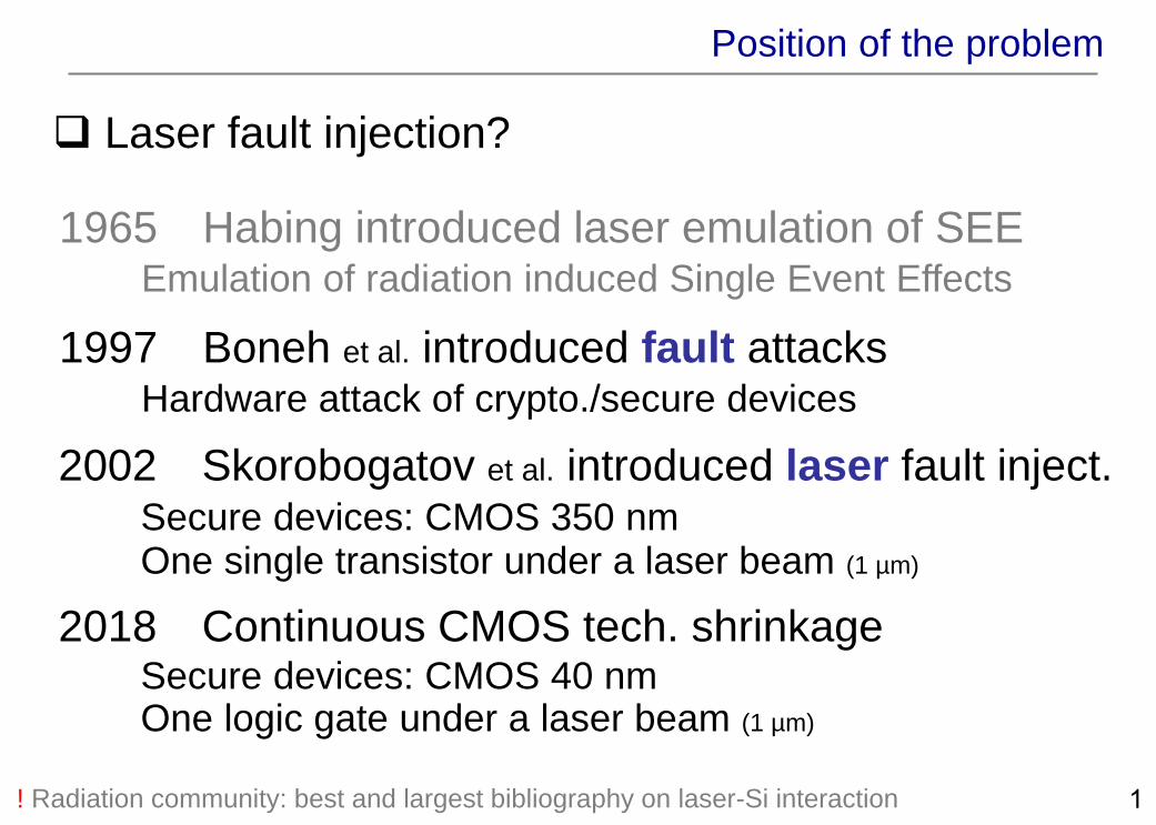
Laser fault injection?
1997 Boneh et al. introduced fault attacksHardware attack of crypto./secure devices
2002 Skorobogatov et al. introduced laser fault inject.Secure devices: CMOS 350 nmOne single transistor under a laser beam (1 µm)
2018 Continuous CMOS tech. shrinkageSecure devices: CMOS 40 nmOne logic gate under a laser beam (1 µm)
1965 Habing introduced laser emulation of SEEEmulation of radiation induced Single Event Effects
! Radiation community: best and largest bibliography on laser-Si interaction 1

Position of the problem
Laser fault injection?
Pulsed lasers are used to inject faults into running secure
devices for the purpose of retrieving secret information.
Why does it matters?
An efficient fault injection tool
An accurate fault injection tool
Part of security certification processes
2
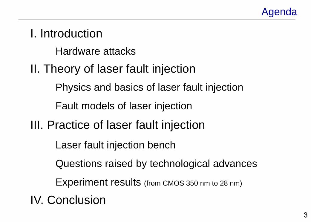
Agenda
I. Introduction
Hardware attacks
II. Theory of laser fault injection
Physics and basics of laser fault injection
Fault models of laser injection
IV. Conclusion
III. Practice of laser fault injection
Laser fault injection bench
Questions raised by technological advances
Experiment results (from CMOS 350 nm to 28 nm)
3

I. Introduction
Frequency
Power
100 W10 mW 104
1
02
3 G
Hz
10 M
Hz
Tomorrow's secure
devices?
Secure devices
Secure devices
4
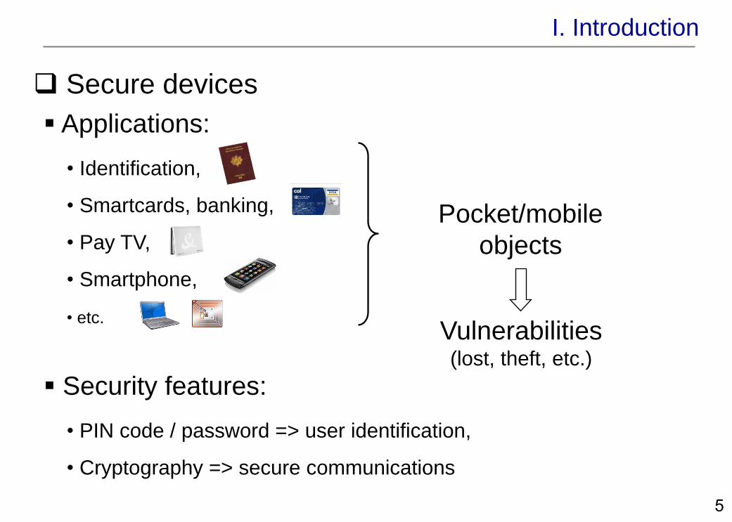
• Identification,
• Smartcards, banking,
• Pay TV,
• Smartphone,
• etc.
Applications:
Pocket/mobile
objects
Vulnerabilities (lost, theft, etc.)
• PIN code / password => user identification,
• Cryptography => secure communications
Security features:
I. Introduction
Secure devices
5
I. Introduction
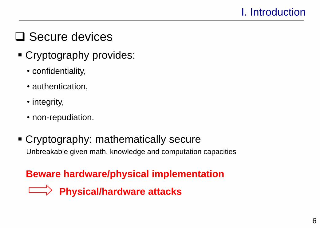
• confidentiality,
• authentication,
• integrity,
• non-repudiation.
Cryptography provides:
Secure devices
Beware hardware/physical implementation
Physical/hardware attacks
Unbreakable given math. knowledge and computation capacities
Cryptography: mathematically secure
6
I. Introduction
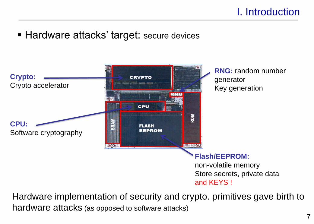
Hardware attacks’ target: secure devices
Crypto:
Crypto accelerator
Flash/EEPROM:
non-volatile memory
Store secrets, private data
and KEYS !
CPU:
Software cryptography
RNG: random number
generator
Key generation
Hardware implementation of security and crypto. primitives gave birth to
hardware attacks (as opposed to software attacks)
7
FLASH

I. Introduction
Hardware attacks
Goal: retrieve secret information or encryption keys, PIN bypass, gain
unauthorized access, etc.
• encryption time,
• power consumption (which correlates with the handled data),
• EM emissions (which correlates with the handled data),
• photon emission, etc.
Observation attacks: passive attacks
Observation/eavesdropping of a physical parameter that is
correlated to the data handled by the target circuit.
8
I. Introduction
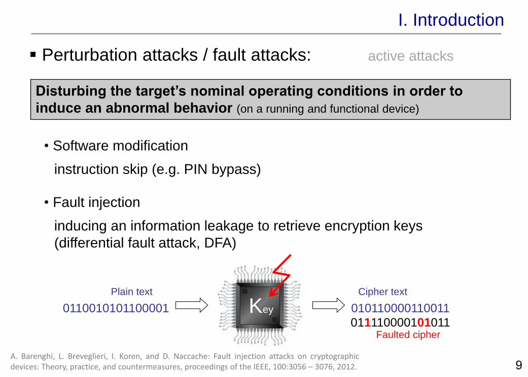
Perturbation attacks / fault attacks: active attacks
Disturbing the target’s nominal operating conditions in order to
induce an abnormal behavior (on a running and functional device)
• Software modification
instruction skip (e.g. PIN bypass)
• Fault injection
inducing an information leakage to retrieve encryption keys
(differential fault attack, DFA)
Key
Plain text
0110010101100001 010110000110011
Cipher text
011110000101011Faulted cipher
A. Barenghi, L. Breveglieri, I. Koren, and D. Naccache: Fault injection attacks on cryptographicdevices: Theory, practice, and countermeasures, proceedings of the IEEE, 100:3056 – 3076, 2012. 9

I. Introduction
C. Giraud: DFA on AES, Lecture Notes in Computer Science, 2005, Springer Berlin / Heidelberg,Volume 3373
G. Piret, J.-J. Quisquater: A Differential Fault Attack Technique Against SPN Structures, withApplication to the AES, CHES 2003, LNCS 2779, Springer-Verlag
• location (e.g. round calculations or key expansion),
• injection time (regarding the course of the algorithm),
• nb. of faulted bits/bytes
Strong fault model:
Requirements of the fault injection process?
Single-bit / single-byte fault models associated with very efficient
DFA schemes
The attacker needs a fine control on the fault injection process
10
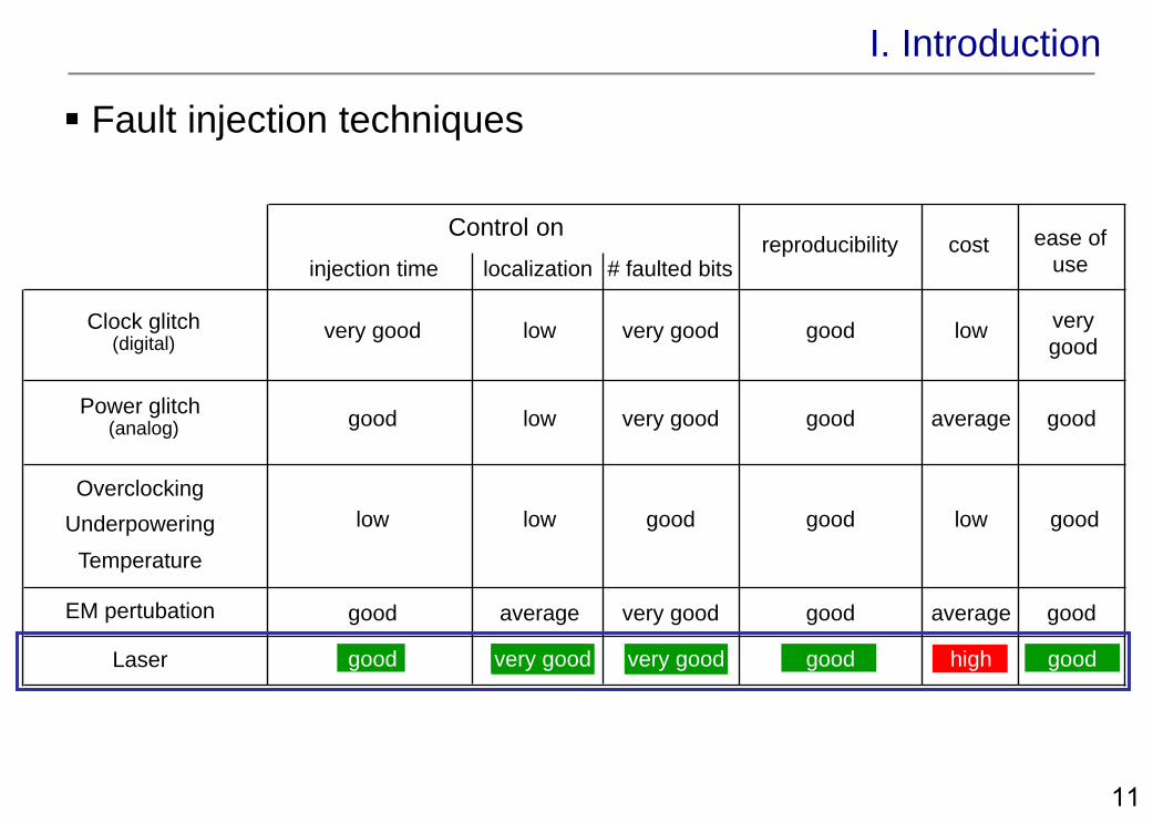
I. Introduction
Fault injection techniques
injection time
Control on
localization # faulted bitsreproducibility cost ease of
use
Clock glitch(digital)
Power glitch(analog)
Overclocking
Underpowering
Temperature
EM pertubation
very good low very good good low very
good
good low very good good average good
low low good good low good
Laser good très bon good high goodvery good very good
good average very good good average good
11

Laser fault injection
S. P. Skorobogatov and R. J. Anderson: Optical fault induction attacks, CHES 2002.
D. Habing: The use of lasers to simulate radiation-induced transients in semiconductor devicesand circuits. Nuclear Science, IEEE Transactions on, 12(5):91–100, Oct 1965.
- radioactive effects emulation (1965, D. Habing),
- 1st publication related to secure devices in 2002 (S. Skorobogatov).
• An efficient fault injection tool
Why considering this costly FI technique?
- location / timing / focalization (nb. of faulted bits).
• An accurate fault injection tool
- part of the certification process of secure devices,
- high level of certification mandatory to access secure devices market
• Security certification (common criteria/EAL)
I. Introduction
12

Agenda
I. Introduction
Hardware attacks
II. Theory of laser fault injection
Physics and basics of laser fault injection
Fault models of laser injection
IV. Conclusion
III. Practice of laser fault injection
Laser fault injection bench
Questions raised by technological advances
Experiment results (from CMOS 350 nm to 28 nm)
13

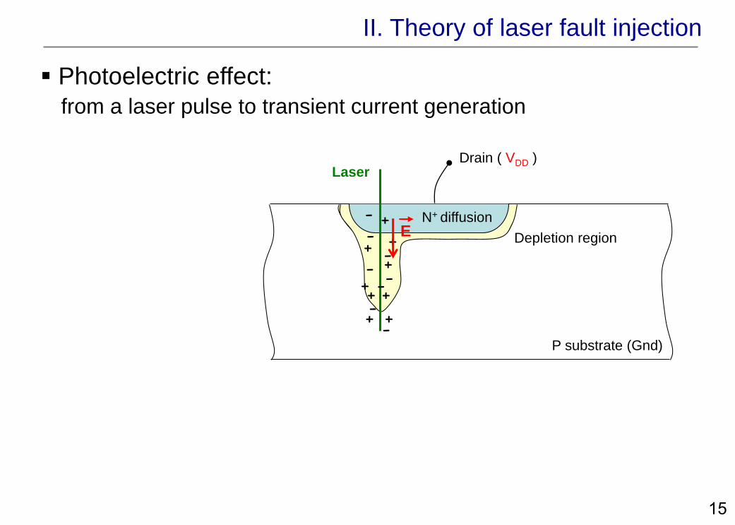
Physics of laser fault injection
Front side
Backside
Laser beam: semi invasive (package mechanical/chemical opening)
• laser – silicon interaction: the photoelectric effect
laser 1,1 m
Energy (eV) EC
h
EV
h Eg
II. Theory of laser fault injection
14

• Front side: reflection on metal paths (e.g. 532nm, green)
• Backside: = infrared (e.g. 1064nm) (die thinning)
Physics of laser fault injection
Laser beam: semi invasive (package mechanical/chemical opening)
Front side
Backside
II. Theory of laser fault injection
14

Photoelectric effect:
Drain ( Gnd )
N+ diffusion
Laser
-
+++
+++
++
-+
----
-
-P substrate (Gnd)
II. Theory of laser fault injection
from a laser pulse to transient current generation
15
Drain ( VDD )
Photoelectric effect:
N+ diffusion
Laser
-
+++
+++
++
-+
----
-
-
Depletion regionE
P substrate (Gnd)
II. Theory of laser fault injection
from a laser pulse to transient current generation
15

Photoelectric effect:
Transient current
Laser sensitive areas: reverse biased PN junctions
II. Theory of laser fault injection
from a laser pulse to transient current generation
Drain ( VDD )
N+ diffusion
Laser
-
+++
+++
++
-+
----
-
-
Depletion regionE
P substrate (Gnd)
15

laser beam
P substrate
N well
P+
Cout ‘1’
to Vdd
P+ N+N+ N+P+
to Gnd
in ‘0’
NMOS PMOS
Metal 1
MOS gate
OFF
ON
Fault injection mechanism (the inverter case)
II. Theory of laser fault injection
from a transient current to a voltage transient (a.k.a. SET, single event transient)
16
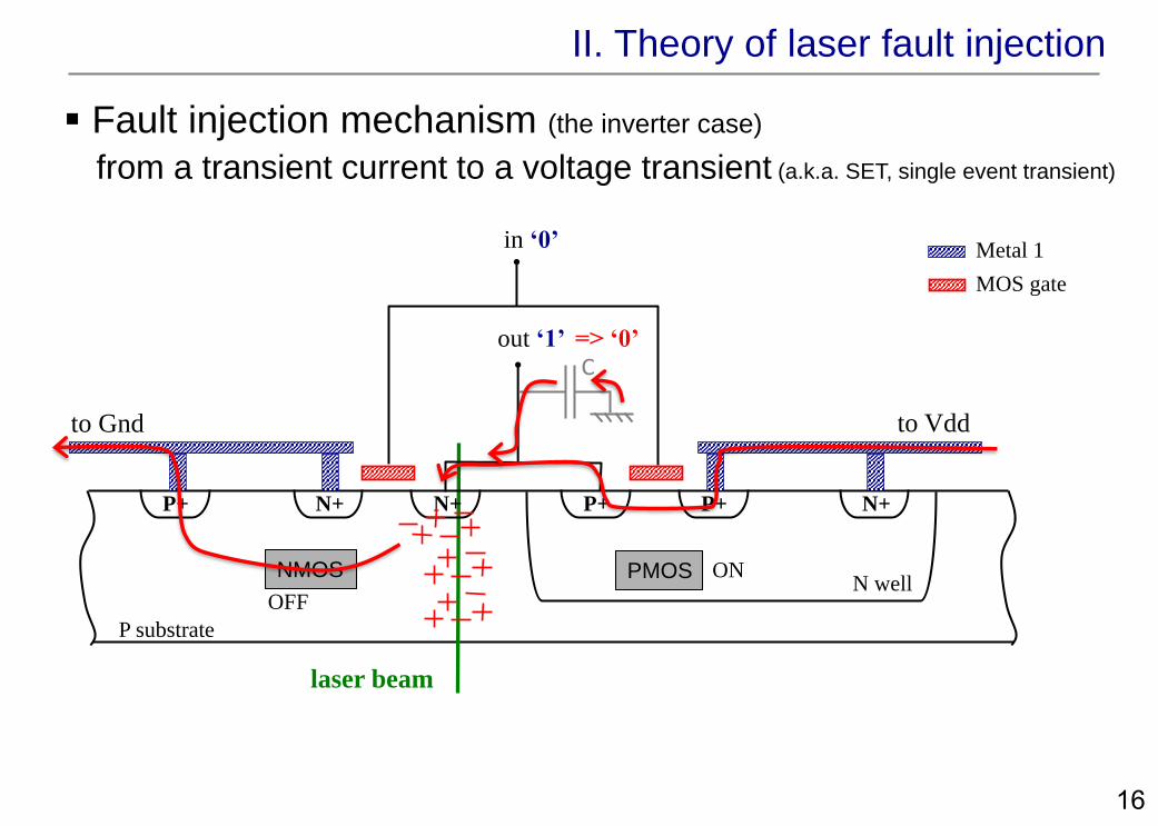
laser beam
P substrate
N well
P+
Cout ‘1’
to Vdd
P+ N+N+ N+P+
to Gnd
in ‘0’
NMOS PMOS
Metal 1
MOS gate
OFF
ON
Fault injection mechanism (the inverter case)
II. Theory of laser fault injection
from a transient current to a voltage transient (a.k.a. SET, single event transient)
=> ‘0’
16

P substrate
N well
P+
Cout ‘1’
to Vdd
P+ N+N+ N+P+
to Gnd
in ‘0’
NMOS PMOS
Metal 1
MOS gate
OFF
ON
Fault injection mechanism (the inverter case)
II. Theory of laser fault injection
from a transient current to a voltage transient (a.k.a. SET, single event transient)
=> ‘0’
16

P substrate
N well
P+
Cout ‘1’
to Vdd
P+ N+N+ N+P+
to Gnd
in ‘0’
NMOS PMOS
Metal 1
MOS gate
Laser sensitive areas: OFF transistors’ drains (reversed biased PN junctions)
OFF
ON
Fault injection mechanism (the inverter case)
II. Theory of laser fault injection
from a transient current to a voltage transient (a.k.a. SET, single event transient)
16
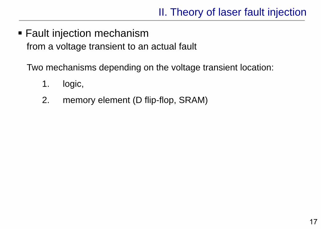
Fault injection mechanism
II. Theory of laser fault injection
from a voltage transient to an actual fault
1. logic,
2. memory element (D flip-flop, SRAM)
Two mechanisms depending on the voltage transient location:
17

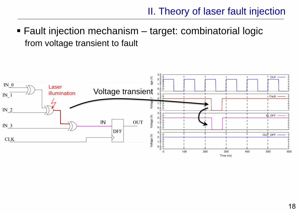
Fault injection mechanism – target: combinatorial logic
II. Theory of laser fault injection
from voltage transient to fault
18
IN
Laser
illumination
Voltage transient
Fault injection mechanism – target: combinatorial logic
II. Theory of laser fault injection
from voltage transient to fault
18
IN
Laser
illumination

Voltage transient
Fault injection mechanism – target: combinatorial logic
II. Theory of laser fault injection
from voltage transient to fault
18
IN
Laser
illumination
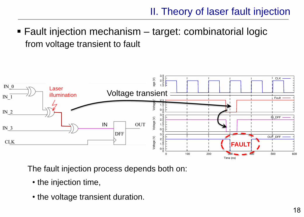
The fault injection process depends both on:
• the injection time,
• the voltage transient duration.
Voltage transient
Fault injection mechanism – target: combinatorial logic
II. Theory of laser fault injection
from voltage transient to fault
FAULT
18
IN
Laser
illumination

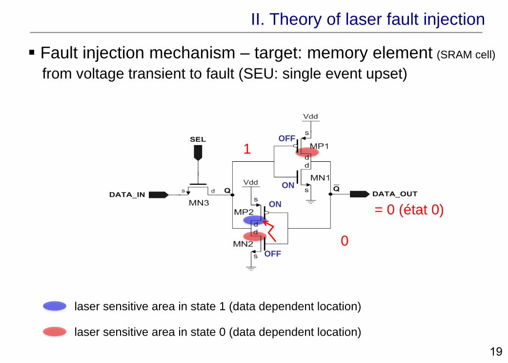
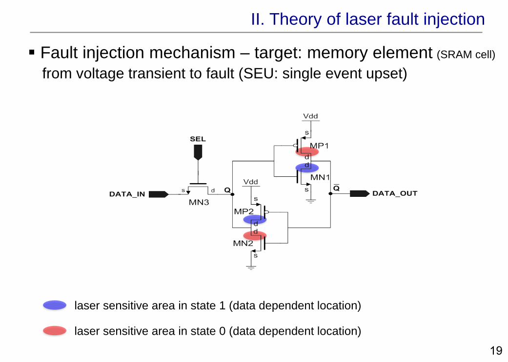
Fault injection mechanism – target: memory element (SRAM cell)
II. Theory of laser fault injection
from voltage transient to fault (SEU: single event upset)
OFF
ON
OFF
ON
laser sensitive area in state 1 (data dependent location)
0
= 1 (state 1)
1
19

Fault injection mechanism – target: memory element (SRAM cell)
II. Theory of laser fault injection
OFF
ON
OFF
ON
laser sensitive area in state 1 (data dependent location)
0
= 1 (state 1)
1
=> 1
19
from voltage transient to fault (SEU: single event upset)
Fault injection mechanism – target: memory element (SRAM cell)
II. Theory of laser fault injection
OFF
ON
OFF
ON
laser sensitive area in state 1 (data dependent location)
0
= 1 (state 1)
1
=> 1OFF
ON
=> 00
1
= 0 (état 0)
laser sensitive area in state 0 (data dependent location)
OFF
ON
19
from voltage transient to fault (SEU: single event upset)
Fault injection mechanism – target: memory element (SRAM cell)
II. Theory of laser fault injection
laser sensitive area in state 1 (data dependent location)
laser sensitive area in state 0 (data dependent location)
19
from voltage transient to fault (SEU: single event upset)
Agenda
I. Introduction
Hardware attacks
II. Theory of laser fault injection
Physics and basics of laser fault injection
Fault models of laser injection
IV. Conclusion
III. Practice of laser fault injection
Laser fault injection bench
Questions raised by technological advances
Experiment results (from CMOS 350 nm to 28 nm)
20

Fault model:
II. Theory of laser fault injection
Often expressed as the number of faulted bits and the injection time, e.g.:
• Giraud DFA on AES (single bit, 9th round )
• Piret et al. DFA on AES (single byte, between last two MixColumns)
requirements to be fulfilled to succeed in a given fault
attack scheme
Disturbing the target’s nominal operating conditions in order to
induce an abnormal behavior/calculation (ie injecting a fault)
while satisfying the fault model and without destroying the target.
remember that a fault attack consists in:
21

Fault model: mathematical expression at bit level
II. Theory of laser fault injection
bit-flip (usual fault model, data independent)
b not (b )
22

bit-set/reset fault model (data dependent)
if b 0 b 1
if b 1 b 1
Fault model: mathematical expression at bit level
II. Theory of laser fault injection
bit-set
if b 0 b 0
if b 1 b 0bit-reset
Provide additional information on the original bit value
Safe error attack (e.g. retrieveing memory bits)
23

9µ
m
Vdd
Gnd
SEL
Q
data
_out
MP1
MN1
MP2
MN2
MN3
4µm
Metal 1
MOS gate
Diffusion
Laser spot size/effect area:
1µm
Laser sensitive areas:
state 1
state 0
bit-set/reset fault model of memory elements: 5T SRAM cell
II. Theory of laser fault injection
One laser sensitive area exposed
bit-set/reset fault model
24

9µ
m
Vdd
Gnd
SEL
Q
data
_out
MP1
MN1
MP2
MN2
MN3
4µm
Metal 1
MOS gate
Diffusion
Laser spot size/effect area:
3 µm
Laser sensitive areas:
state 1
state 0
bit-set/reset fault model of memory elements: 5T SRAM cell
II. Theory of laser fault injection
Overlaps of laser sensitive areas
bit-flip fault model
Overlaps
25

bit-set/reset fault model of memory elements: 5T SRAM cell
II. Theory of laser fault injection
Q? fault model of memory elements:
• bit-flip, data independent
• bit-set/reset, data dependent (safe error attacks)
Q? feasibility of single bit/byte fault model
Q? with respect to technology shrinkage
other fault model issues
26
Agenda
I. Introduction
Hardware attacks
II. Theory of laser fault injection
Physics and basics of laser fault injection
Fault models of laser injection
IV. Conclusion
III. Practice of laser fault injection
Laser fault injection bench
Questions raised by technological advances
Experiment results (from CMOS 350 nm to 28 nm)
27
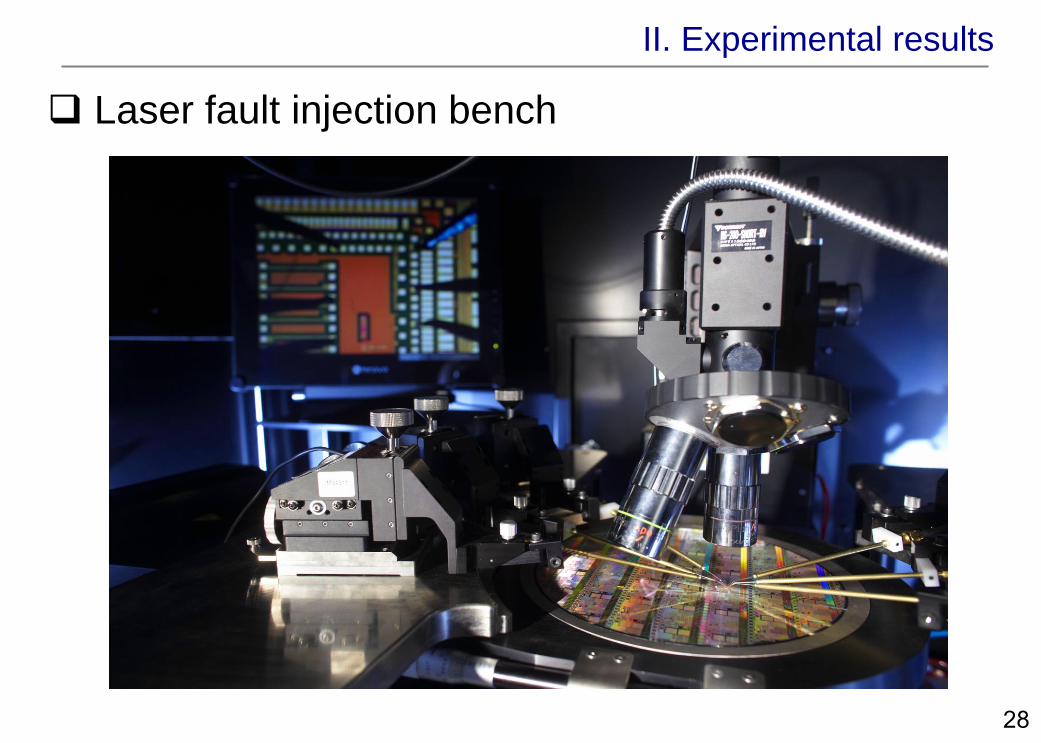
II. Experimental results
Laser fault injection bench
28
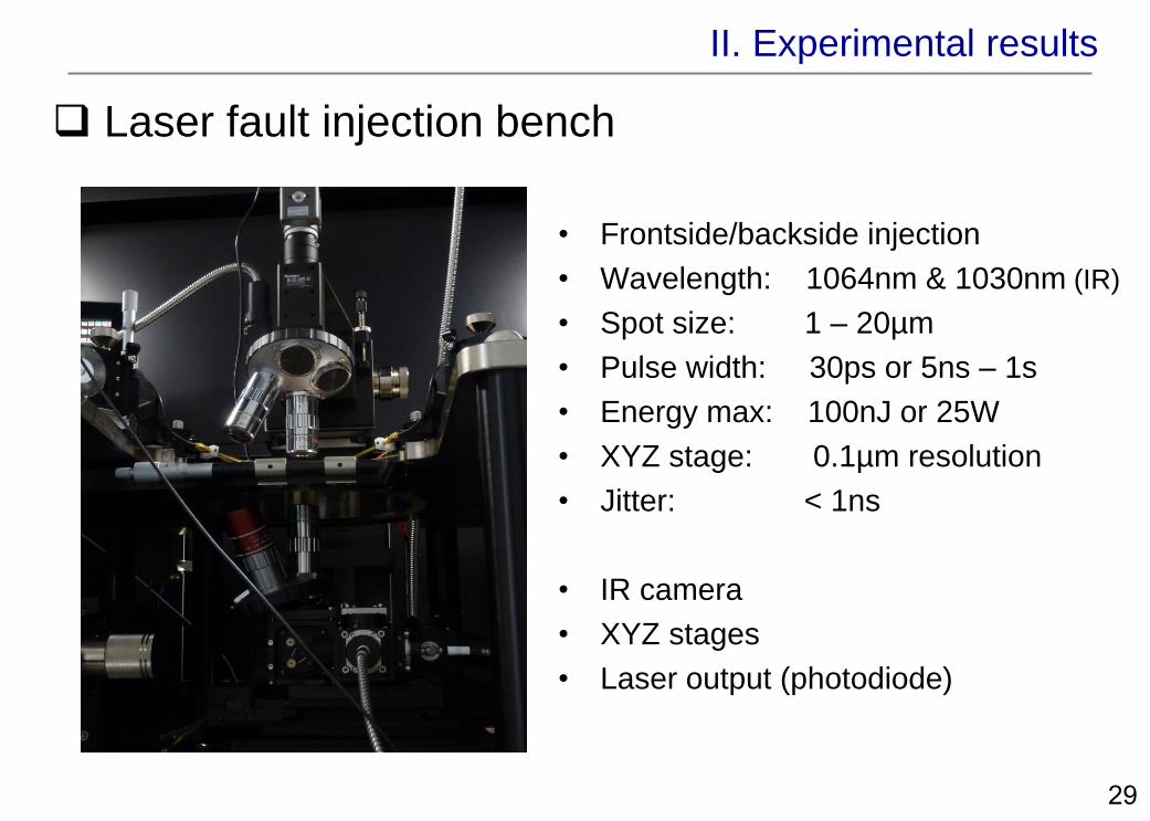
• Frontside/backside injection
• Wavelength: 1064nm & 1030nm (IR)
• Spot size: 1 – 20µm
• Pulse width: 30ps or 5ns – 1s
• Energy max: 100nJ or 25W
• XYZ stage: 0.1µm resolution
• Jitter: < 1ns
• IR camera
• XYZ stages
• Laser output (photodiode)
II. Experimental results
Laser fault injection bench
29

II. Experimental results
x
y
Laser fault injection bench: laser sensitivity maps
Laser head
30
Agenda
I. Introduction
Hardware attacks
II. Theory of laser fault injection
Physics and basics of laser fault injection
Fault models of laser injection
IV. Conclusion
III. Practice of laser fault injection
Laser fault injection bench
Questions raised by technological advances
Experiment results (from CMOS 350 nm to 28 nm)
31

SRAM
0.35 µm
130 nm
90 nm
65 nm
1 µm
MOS transistor Technology
Laser spot
28 nm
Single-bit/byte fault model validity?
II. Experimental results
32

SRAM
0.35 µm
130 nm
90 nm
65 nm
1 µm
MOS transistor Technology
Laser spot
28 nm
Single-bit/byte fault model validity?
II. Experimental results
32
Simultaneous flip of several
SRAMs?

Agenda
I. Introduction
II. Theory of laser fault injection
IV. Conclusion
III. Practice of laser fault injection
Laser fault injection bench
Questions raised by technological advances
Experiment results (from CMOS 350 nm to 28 nm)
- memory elements
- microcontroller
- ASIC
33
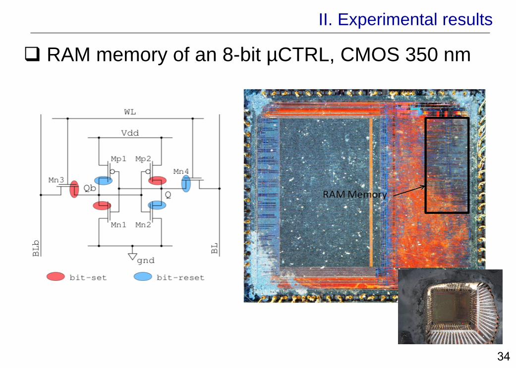
RAM memory of an 8-bit µCTRL, CMOS 350 nm
II. Experimental results
34

bit set (0 1)
bit reset (1 0)
RAM memory of an 8-bit µCTRL, CMOS 350 nm
II. Experimental results
spot 1 µm / 30 ps / 2.4 nJ / ∆xy = 0.2 µm / backside
Laser-sensitivity map
SRAM cell
35

RAM memory of an 8-bit µCTRL, CMOS 350 nm
II. Experimental results
spot 1 µm / 30 ps / 2.4 nJ / ∆xy = 0.2 µm / backside
Single-bit fault model achieved
Consistent with the theory (4 sensitive areas)
C. Roscian, A. Sarafianos, J.-M. Dutertre, and A. Tria. Fault model analysis of laser-induced faults in SRAM memory cells.In 2013 Workshop on Fault Diagnosis and Tolerance in Cryptography, 2013. 36

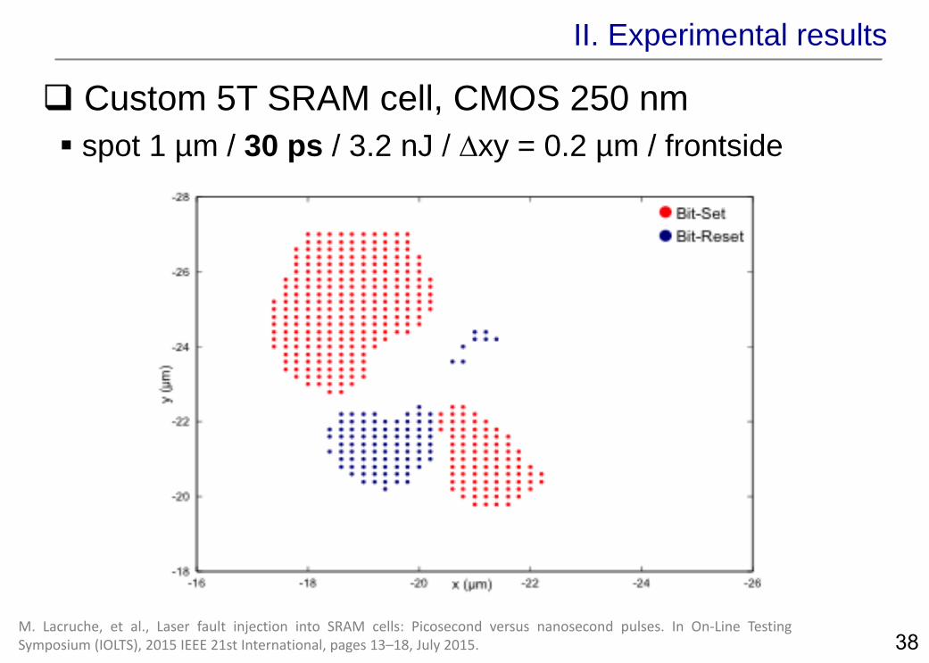
Custom 5T SRAM cell, CMOS 250 nm
II. Experimental results
spot 1 µm / 30 ps / 3.2 nJ / ∆xy = 0.2 µm / frontside
4 µm x 9 µm
37
Custom 5T SRAM cell, CMOS 250 nm
II. Experimental results
spot 1 µm / 30 ps / 3.2 nJ / ∆xy = 0.2 µm / frontside
M. Lacruche, et al., Laser fault injection into SRAM cells: Picosecond versus nanosecond pulses. In On-Line TestingSymposium (IOLTS), 2015 IEEE 21st International, pages 13–18, July 2015. 38

Custom D flip-flop, CMOS 40 nm
II. Experimental results
schematic
39

Custom D flip-flop, CMOS 40 nm
II. Experimental results
layout
40
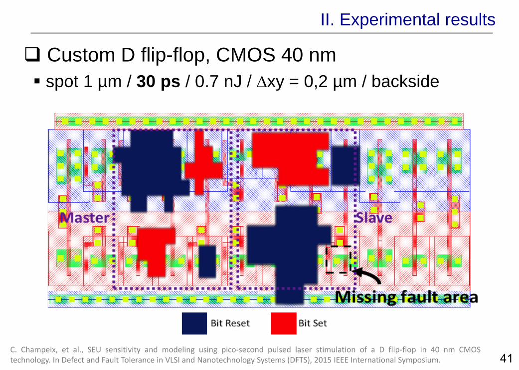
Custom D flip-flop, CMOS 40 nm
II. Experimental results
spot 1 µm / 30 ps / 0.7 nJ / ∆xy = 0,2 µm / backside
C. Champeix, et al., SEU sensitivity and modeling using pico-second pulsed laser stimulation of a D flip-flop in 40 nm CMOStechnology. In Defect and Fault Tolerance in VLSI and Nanotechnology Systems (DFTS), 2015 IEEE International Symposium. 41

Custom D flip-flop registers, CMOS 28 nm
II. Experimental results
J.-M. Dutertre, et al., Assessment of the laser-induced fault model towards continuous cmostechnology shrinkage. TRUDEVICE Workshop, Dresden Germany, March 2016. 42

Custom D flip-flop registers, CMOS 28 nm
II. Experimental results
Matrix shaped shift register with 64 D flip-flops
Dff
vdd
gnd
clk
D Q
~ 4.3 µm
~ 1
.2 µ
m
- DFF: ~ 40 transistors,
- large output buffer
43
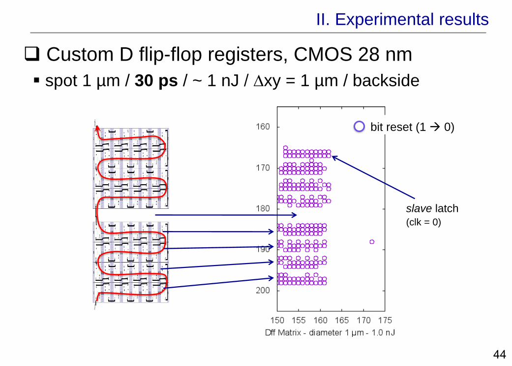
Custom D flip-flop registers, CMOS 28 nm
II. Experimental results
bit reset (1 0)
slave latch
(clk = 0)
spot 1 µm / 30 ps / ~ 1 nJ / ∆xy = 1 µm / backside
44

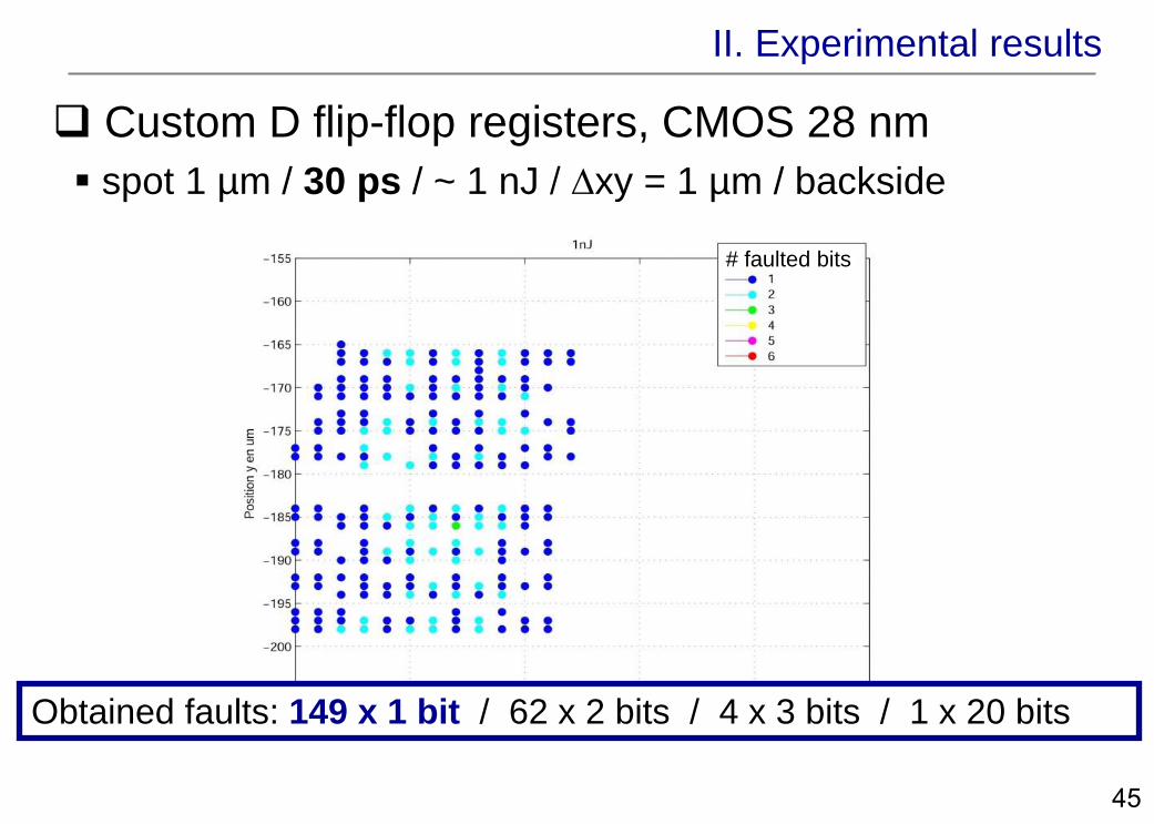
Custom D flip-flop registers, CMOS 28 nm
II. Experimental results
spot 1 µm / 30 ps / ~ 1 nJ / ∆xy = 1 µm / backside
# faulted bits
45
Custom D flip-flop registers, CMOS 28 nm
II. Experimental results
Obtained faults: 149 x 1 bit / 62 x 2 bits / 4 x 3 bits / 1 x 20 bits
spot 1 µm / 30 ps / ~ 1 nJ / ∆xy = 1 µm / backside
# faulted bits
45

Custom D flip-flop registers, CMOS 28 nm
II. Experimental results
3D view
# faulted bits
rank #
in s
hift
regis
ter
46
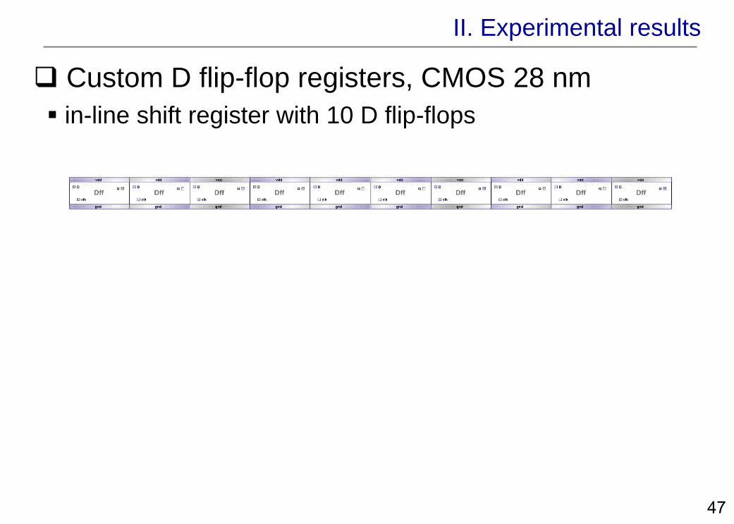
Custom D flip-flop registers, CMOS 28 nm
II. Experimental results
in-line shift register with 10 D flip-flops
47

Custom D flip-flop registers, CMOS 28 nm
II. Experimental results
clk = 0 (slave latch) clk = 1 (master latch)
spot 1 µm / 30 ps / ~ 1 nJ / ∆xy = 0.2 µm / backside
48

Memory elements – Conclusion
Bit-set/reset fault model = relevant
Single-bit fault model experimentally assessed with a laser
up to the CMOS 28 nm node.
Should be taken into account for threat evaluation.
Well defined laser-sensitive areas: implication at 14 nm?
II. Experimental results
49

Agenda
I. Introduction
II. Theory of laser fault injection
IV. Conclusion
III. Practice of laser fault injection
Laser fault injection bench
Questions raised by technological advances
Experiment results (from CMOS 350 nm to 28 nm)
- memory elements
- microcontroller
- ASIC
50
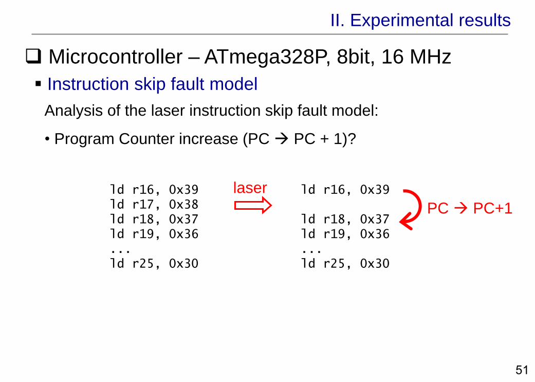
Microcontroller – ATmega328P, 8bit, 16 MHz
II. Experimental results
Instruction skip fault model
ld r16, 0x39
ld r17, 0x38
ld r18, 0x37
ld r19, 0x36
...
ld r25, 0x30
ld r16, 0x39
ld r18, 0x37
ld r19, 0x36
...
ld r25, 0x30
Analysis of the laser instruction skip fault model:
• Program Counter increase (PC PC + 1)?
laser
PC PC+1
51

Microcontroller – ATmega328P, 8bit, 16 MHz
II. Experimental results
Instruction skip fault model
ld r16, 0x39
ld r17, 0x38
ld r18, 0x37
ld r19, 0x36
...
ld r25, 0x30
ld r16, 0x39
nop
ld r18, 0x37
ld r19, 0x36
...
ld r25, 0x30
Analysis of the laser instruction skip fault model:
• Instruction alteration (no operation, nop or changed)?
laser
Single nop
52
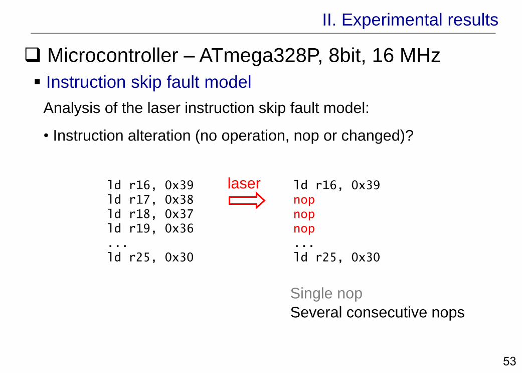
Microcontroller – ATmega328P, 8bit, 16 MHz
II. Experimental results
Instruction skip fault model
ld r16, 0x39
ld r17, 0x38
ld r18, 0x37
ld r19, 0x36
...
ld r25, 0x30
ld r16, 0x39
nop
nop
nop
...
ld r25, 0x30
Analysis of the laser instruction skip fault model:
• Instruction alteration (no operation, nop or changed)?
laser
Single nop
Several consecutive nops
53

T. Riom, J.-M. Dutertre, O. Potin, and J.-B. Rigaud. Practical results on laser-induced instruction- skip attacks intomicrocontrollers. TRUDEVICE Workshop, Barcelon Spain, 2016.
Microcontroller – ATmega328P, 8bit, 16 MHz
II. Experimental results
Instruction skip fault model
ld r16, 0x39
ld r17, 0x38
ld r18, 0x37
ld r19, 0x36
...
ld r25, 0x30
ld r16, 0x39
nop
ld r18, 0x37
nop
...
ld r25, 0x30
Analysis of the laser instruction skip fault model:
• Instruction alteration (no operation, nop or changed)?
laser
Several non-consecutive nops
Single nop
Several consecutive nops
54
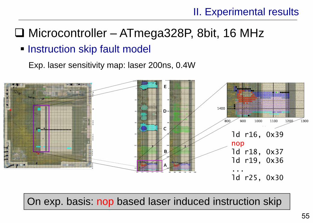
Microcontroller – ATmega328P, 8bit, 16 MHz
II. Experimental results
Instruction skip fault model
Exp. laser sensitivity map: laser 200ns, 0.4W
ld r16, 0x39
nop
ld r18, 0x37
ld r19, 0x36
...
ld r25, 0x30
On exp. basis: nop based laser induced instruction skip
55

Microcontroller – ATmega328P, 8bit, 16 MHz
II. Experimental results
Instruction skip fault model properties
Time control (laser pulse: 75ns, 0.4W)
Injection time (ns)
Faulted r
egis
ter
#
ability to choose the skipped instruction
56

Microcontroller – ATmega328P, 8bit, 16 MHz
II. Experimental results
Instruction skip fault model properties
Pulse duration control (laser pulse: from 75ns, 0.4W)
Laser pulse duration (ns)
Faulted r
egis
ter
#
ability to choose the number of skipped instructions
57

Agenda
I. Introduction
II. Theory of laser fault injection
IV. Conclusion
III. Practice of laser fault injection
Laser fault injection bench
Questions raised by technological advances
Experiment results (from CMOS 350 nm to 28 nm)
- memory elements
- microcontroller
- ASIC
58

ASIC, crypto-accelerator
II. Experimental results
Hardware AES-128, CMOS 28nm, Vdd = 1.2V, 100MHz
59

II. Experimental results
Hardware AES-128, CMOS 28nm, Vdd = 1.2V, 100MHz
Exp.: 5µm spot, 10ns, 0.6-1.0W, ∆xy = 1µm, Piret’s fault model
26,380 faulted cipher texts
Unidentified faults
6,574 (24.9 %)
mainly 5 – 8 faulty bytes (up to12)
Identified faults
mainly single-byte faults
60

II. Experimental results
Hardware AES-128, CMOS 28nm, Vdd = 1.2V, 100MHz
Exp.: 5µm spot, 10ns, 0.6-1.0W, ∆xy = 1µm, Piret’s fault model
Among the 19,806 identified faults
key schedule (round key computation)
16,253 (61.6 %)
datapath (ciphering block)
3,553 (13.5 %)
61
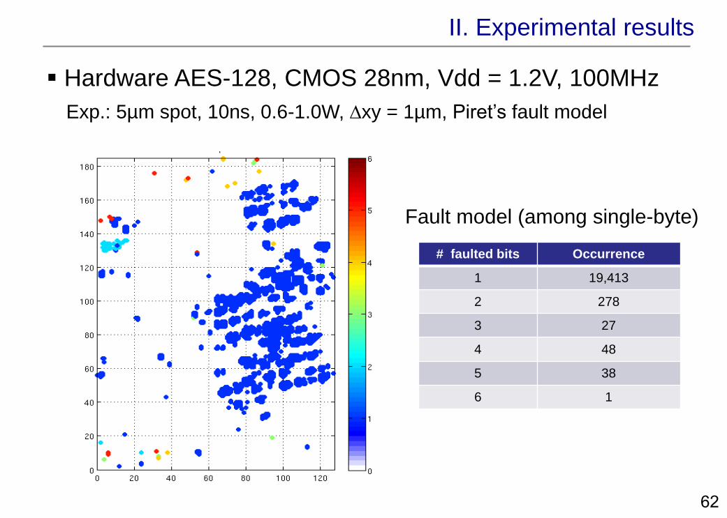
II. Experimental results
Hardware AES-128, CMOS 28nm, Vdd = 1.2V, 100MHz
Exp.: 5µm spot, 10ns, 0.6-1.0W, ∆xy = 1µm, Piret’s fault model
# faulted bits Occurrence
1 19,413
2 278
3 27
4 48
5 38
6 1
Fault model (among single-byte)
62

Agenda
I. Introduction
Hardware attacks
II. Theory of laser fault injection
Physics and basics of laser fault injection
Fault models of laser injection
IV. Conclusion
III. Practice of laser fault injection
Laser fault injection bench
Questions raised by technological advances
Experiment results (from CMOS 350 nm to 28 nm)
63

Conclusion
Introduction to the theory of laser fault injection
Experimental results of laser fault injection
On various targets (µCTRL, memory cells, ASIC)
For various technology nodes: 0.35µm to 28nm CMOS
Key points: assessment of
- the single bit/byte fault model,
- the bit-set/reset fault model,
- the instruction skip (nop) fault model.
Q? at the 14nm node?
Photoelectric effect drain of OFF MOS transistors
64

Merci de votre attention
Département Systèmes et Architectures Sécurisées
Mines Saint-Etienne, Centre de Microélectronique de Provence
13541 Gardanne FRANCE
65