Embed Size (px)
Citation preview
I Ill11 ll111111 Ill Ill11 Ill11 IIIII 11111 11111 11111 11111 11111 llllll Ill1 1111 Ill1 US006713908Bl
(12) United States Patent (io) Patent No.: US 6,713,908 B1 Tai et al. (45) Date of Patent: Mar. 30,2004
USING A MICROMACHINED MAGNETOSTATIC RELAY IN COMMUTATING A DC MOTOR
Inventors: Yu-Chong Tai, Pasadena, CA (US); John A. Wright, Pasadena, CA (US); Gerald Lilienthal, Pasadena, CA (US)
Assignee: California Institute of Technology, Pasadena, CA (US)
Subject to any disclaimer, the term of this patent is extended or adjusted under 35 U.S.C. 154(b) by 0 days.
Notice:
Appl. No.: 09/281,831
Filed: Mar. 30. 1999
Related U.S. Application Data Provisional application No. 601080,063, filed on Mar. 31, 1998.
Int. Cl? ............................. H02K 1/00; H02K 3/00 U.S. C1. ................... 310/68 R; 310168 B; 3101179;
3101180; 310140 MM; 310/DIG. 6; 3181138; 3181251
Field of Search ............................. 310168 B, 68 R,
251; 335178, 80, 38, 205, 154 310140 MM, DIG. 6, 173, 179-180; 3181138,
References Cited
U.S. PATENT DOCUMENTS
3,626,222 A * 1211971 Dischler ...................... 310196 3,900,780 A * 811975 Tanikoshi ................... 3181254
4,475,068 A * 1011984 Brailsford ................... 3181254 5,293,523 A * 311994 Posey ......................... 3351205 5,605,614 A * 211997 Bornand ...................... 205150 5,629,918 A * 511997 Ho et al. .................... 3691112 6,094,116 A * 712000 Tai et al. ...................... 335178
OTHER PUBLICATIONS
Hiroshi Hosaka, et al.; Electromagnetic Microrelays: Con- cepts and Fundamental Characteristics; 1993; IEEE. Joe Drake, et al.; An Electrostatically Actuated Micro-Re- lay; 1995; Proc. Transducers '95, Stockholm, Sweden, vol.
John Wright, et al.; Magnetostatic MEMS Relays for the Miniaturization of Brushless DC Motor Controllers; Jan. 1999; MEMS '99 Conference.
* cited by examiner
Primary Examine rxa r l Tamai Assistant Examiner-J. Aguirrechea (74) Attorney, Agent, or F i r m C i s h & Richardson P.C.
(57) ABSTRACT
A DC motor is commutated by rotating a magnetic rotor to induce a magnetic field in at least one magnetostatic relay in the motor. Each relay is activated in response to the mag- netic field to deliver power to at least one corresponding winding connected to the relay. In some cases, each relay delivers power first through a corresponding primary wind- ing and then through a corresponding secondary winding to a common node. Specific examples include a four-pole, three-phase motor in which each relay is activated four times during one rotation of the magnetic rotor.
2, pp. 380-383.
14 Claims, 6 Drawing Sheets
f
606
https://ntrs.nasa.gov/search.jsp?R=20080005088 2020-03-25T14:41:20+00:00Z
U S . Patent Mar. 30,2004
I
Sheet 1 of 6
125- 1 I O
US 6,713,908 B1
120 / , r l 0 5 135 I
I 115
FIG. 1A
H
110
FIG. I B
210
FIG. 2A
H
7 205 7
1 210
FIG. 2B
U.S. Patent Mar. 30,2004 Sheet 2 of 6
FIG. 3A
f- 330 ,- 330
FIG. 3B
US 6,713,908 B1
340
335
FIG. 3C
U S . Patent Mar. 30,2004 Sheet 3 of 6 US 6,713,908 B1
FIG. 4A FIG. 4B
FIG. 4C FIG. 4 0
440 7
FIG. 4E
U S . Patent Mar. 30,2004 Sheet 4 of 6
530a
5306
t- !joo 520 7 515 -, B 530b
- 535
530c
FIG. 5A
580a
575a
575b
580b
US 6,713,908 B1
6 505
FIG. 5B
510
FIG. 5C
U S . Patent Mar. 30,2004 Sheet 5 of 6 US 6,713,908 B1
FIG. 6
U S . Patent Mar. 30,2004 Sheet 6 of 6 US 6,713,908 B1
FIG. 7
US 6,713,908 B3 2
made very small using micromachining fabrication techniques, and the materials are carefully selected to pro- vide high reliability. The switches are useful in a wide variety of microelectronic mechanical system (MEMS)
5 applications, particularly in the miniaturization of DC elec- tric motors. For example, in one embodiment of the invention, the switches are used as relays in a MEMS circuit that replaces the conventional commutation and control electronics in a DC motor. This MEMS circuit is much smaller than the DC motor itself, so the size of the motor, not the size of the commutation electronics, is most critical in space constrained applications. The magnetostatic switch requires no biasing current or voltage and is useful in directly switching loads.
In one aspect, the invention features a DC motor having a plurality of windings and at least one magnetostatic relay positioned to activate in the presence of a magnetic field. Each relay is connected electrically to at least one corre- sponding winding and to power. The motor also includes a
2o magnetic rotor having at least one pole positioned to induce a magnetic field in each magnetostatic relay when passing by the relay.
In some embodiments, the windings are arranged in pairs of primary and secondary windings, and each relay connects
2s to a corresponding one of the pairs of windings. In some cases the secondary windings all connect to a common node, and each of the primary windings connects to the corre- sponding relay. In one implementation, the motor is a four-pole, three-phase motor that includes three relays sepa-
In another aspect, the invention features a DC motor having a plurality of windings and at least one magnetostatic relay connected electrically to at least one of the windings and to power. Each relay has at least one substrate formed
3s from a non-conductive or semiconductive material, a spring- ing beam formed on the substrate, and two electrically conductive elements, one of which is formed on the spring- ing beam. The electrically conductive-elements together define at least two-switching states, including an open state
40 in which the conductive elements are physically separated from each other, and a closed state in which the conductive elements physically contact each other. The springing beam includes a magnetic material which, in the presence of a magnetic field, creates an actuation force that causes the
4s electrically conductive elements to apply power to or remove power from at least one of the windings by switch- ing from one of the switching states to another of the switching states. The motor also includes a magnetic rotor having at least one pole positioned to induce a magnetic field
In another aspect, the invention features a method for use in commutating a DC motor. The method includes rotating a magnetic rotor to induce a magnetic field in at least one magnetostatic relay in the motor. Each relay is activated in
5s response to the magnetic field to deliver power to at least one winding in the motor.
In some embodiments, each relay first delivers power through a corresponding primary winding and then through a corresponding secondary winding to a common node.
60 Other embodiments include activating each relay four times during one rotation of the magnetic rotor.
Other embodiments and advantages will become apparent from the following description and from the claims.
1s
30 rated from each other by approximately 120".
so in each magnetostatic relay when passing by the relay.
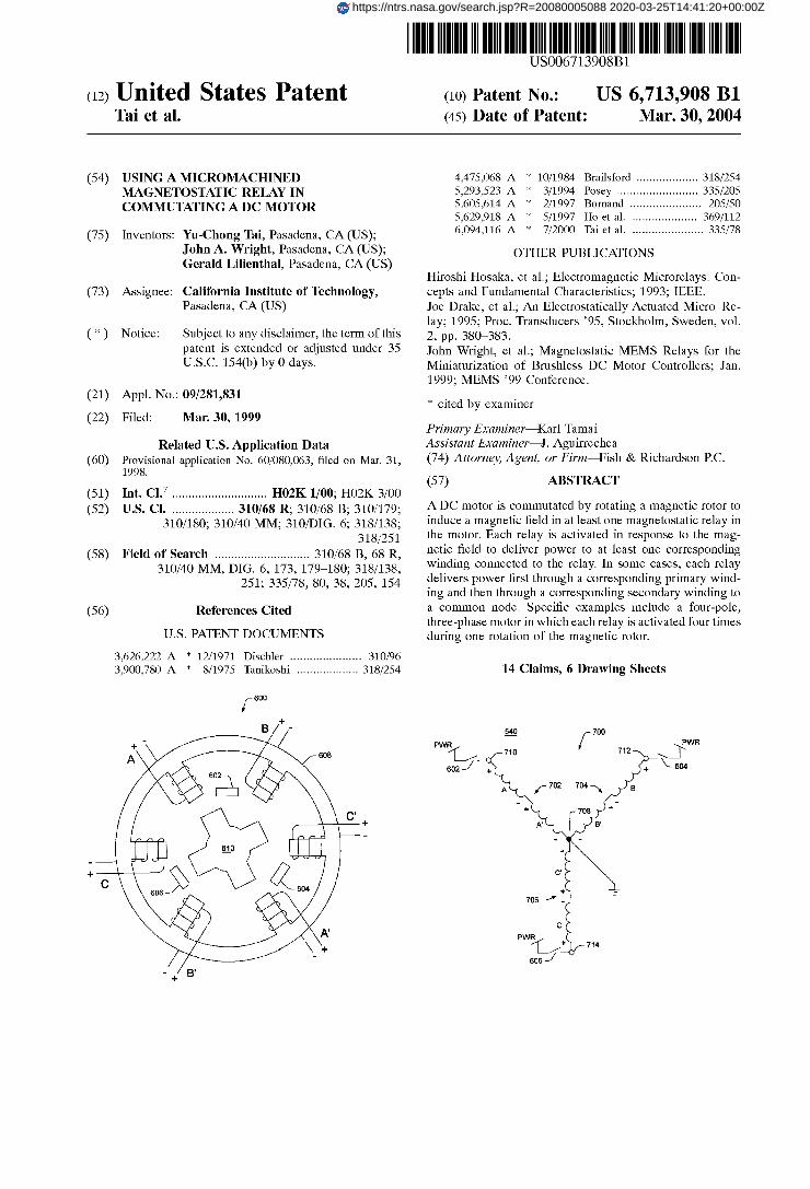
DESCRIPTION OF THE DRAWINGS 65 FIGS. 1 A and 1B are simplified diagrams of a normally-
open magnetostatic switch.
1 USING A MICROMACHINED MAGNETOSTATIC RELAY IN
COMMUTATING A DC MOTOR
CROSS REFERENCE TO RELATED APPLICATIONS
This application claims the benefit of U.S. Provisional Application No. 601080,063, filed on Mar. 31, 1998.
STATEMENT AS TO FEDERALLY SPONSORED RESEARCH
The invention described herein was made in the perfor- mance of work under a NASA contract, and is subject to the provisions of Public Law 96-517 (35 USC 202) in which the Contractor has elected to retain title.
TECHNOLOGICAL FIELD
The invention relates to miniaturization of electronic components and, in particular, to using a micromachined magnetostatic relay in commutating a DC motor.
BACKGROUND
Manufacturers and users of electrical and electronic com- ponents strive to reduce the size and increase the reliability of these components and the systems in which they are used. Miniaturization of components leads to more compact and lightweight systems, which increases the range of uses for these systems and decreases the costs associated with trans- porting and using these systems. Improving component reliability lengthens the lifespan and enhances the perfor- mance of systems in which the components are used.
Miniaturization and reliability improvements are particu- larly important in areas such as space exploration and satellite communications. The cost of launching equipment from the Earth's surface is directly related to the size and weight of the equipment, and even modest reductions in equipment size produce large reductions in cost. Likewise, improving the reliability of components used in spaceborne systems extends and improves the performance of these systems, thus reducing the associated costs. In general, each newly developed generation of space oriented components and systems must meet or exceed the performance and cost standards set by previous generations.
One example of commonly used components for which size and reliability are particularly important is DC electric motors. DC motors are used widely as motive devices for linear and rotary drives in spaceborne applications. As gains have been made in the miniaturization of DC motors, the size, weight, and complexity of DC motor systems have become dominated by the commutation and control elec- tronics that drive the motors. The disparity between the size of the motor and the size of its control electronics is particularly noticeable in a highly miniaturized motor, such as a commercially available 3-mm diameter motor, the commutation and control electronics of which are more than ten times larger than the motor itself. Even modest reduc- tions in the power budget, complexity, mass, and volume of components such as these produce tremendous gains in the cost and reliability of spaceborne systems.
SUMMARY
In recognition of the above, the inventors have developed micromachined magnetostatic relays or switches that are highly miniaturized and highly reliable. The switches are
US 6,713,908 B1 3 4
FIGS. 2A and 2B are simplified diagrams of a normally- creates a 105 force that opposes the residual stress in the closed magnetostatic switch. beam 105, pulling the contacts 115, 125 apart.
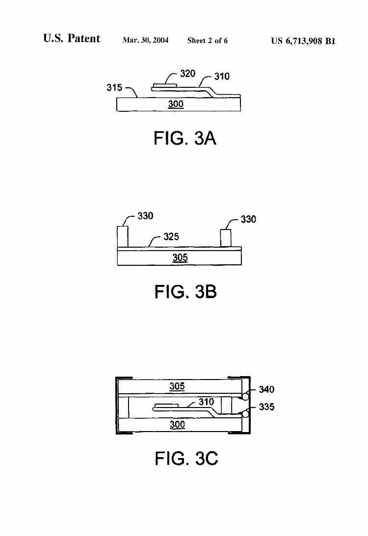
FIGS. 3A, 3B, and 3C are diagrams illustrating, in cross- Several design parameters are considered when designing section, the fabrication of a magnetostatic switch microma- micromachined magnetostatic switches like these. For a chined from two substrates. 5 normally-open switch, these parameters include load
FIGS. 4A, 4B, 4C, 4D, and 4E are perspective views of voltage, maximum current through the switch, operating a substrate at several steps of a two-substrate switch fabri- force (i.e., the force between the contacts when the switch is cation process. closed), contact closing time, and lifetime operations. Table
FIGS, 5A, 5B, and 5c are plan views of substrates in a I below shows typical values for these parameters in three 10 types of switches: conventional electrostatic microswitches, three-substrate switch fabrication process. conventional electromagnetic microswitches, and the micro-
is a plan view Of a DC motor having a MEMS machined magnetostatic switch described here. This table commutation circuit that uses micromachined magnetostatic shows, among other things, that the micromachined mag-
netostatic switch produces much larger contact forces than switches. FIG. 7 is a schematic diagram of the motor windings for 15 the conventional microswitches produce, which reduces
the DC motor of FIG. 6. contact resistance and thus supports much larger operating currents.
DETAILED DESCRIPTION
FIGS. 1 A and 1B show a normally-open microelectronic mechanical system (MEMS) relay or switch 100. The switch 2o
TABLE I
Micromachined 100 includes a cantilever beam 105 mounted on a substrate Electrostatic Electromagnetic Magnetostatic 110. For convenience. the substrate 110 is made from a Parameter Unit Microswitch Microswitch Switch substrate material, such as silicon, that is plentiful and
trical contact 125 made of an electrically .conductive current
load voltage volts 20 20 36 relatively inexpensive. The substrate 110 includes an elec- 25 maximum mA 0.1 100 >so0
contact 125 on the substrate 110. As shown in FIG. lA , the cantilever beam 105 keeps the
electrical contacts 115, 125 separated when the switch 100 is inactive, i.e., when no magnetic field is present. When an external magnetic field H appears, magnetic forces attempt to align the magnetic actuation plate 120 with the magnetic field H, causing the cantilever beam 105 to bend toward the substrate. If the strength of the magnetic field exceeds the design threshold of the switch, the electrical contacts 115, 125 touch, as shown in FIG. lB, completing an electrical circuit through bond wires 130,135. The electrical circuit is
material, such as gold or silver, with a relatively low contact operating mN 0.001 0.1 >1
includes a magnetic actuation plate 120 which, in many contact p e c 20 200 <loo resistance at modest contact forces. The cantilever beam 105
embodiments, is made of a soft magnetic material with high 3o closing time
beam 105 also includes an electrical contact 115, which may or may not be made of the same material that forms the
force contact gap ,um 2 >5 >5
permeability, such as permalloy (Ni80Fe20). The cantilever lifetime cycle >10 million NIA >lo0 million Operations
In most situations, the micromachined magnetostatic 35 switches and the systems in which they are used are
designed to produce large actuation forces, which leads to several additional benefits. Larger actuation forces are present allow a stiffer s cantilever beam, which leads to shorter switching time, higher g-force tolerance, and greater
4o contact breaking force. Greater contact breaking force in turns leads to increased switching lifetime. Large actuation forces also provide the large contact forces, typically between 100 pN and 1 mN, required to yield an acceptable contact resistance when common contact materials, such as
broken when the magnetic field disappears and the restoring 45 silver and gold, are used. The presence of large actuation force of the cantilever beam 105 separates the electrical forces also allows the switches to be designed with large gap contacts 115, 125. In alternative implementations, the can- distances between contacts, which increases device break- tilever beam 105 is designed to separate the contacts 115, down voltage. 125 when the direction Or the magnitude of the magnetic The force generated at the free end of the cantilever beam field changes.
FIGS. 2A and 2B show a normally-closed MEMS switch 200 of similar structure. The cantilever beam 205 in this switch is mounted on the substrate 210 SO that the electrical where T=the thickness of the magnetic actuation plate 120, contacts 215,225 of the beam 205 and the substrate 210 are W=the width of the plate 120, L=the length of the plate 120, held together when the switch 200 is inactive. Applying a 5s e=the deflection angle of the beam 105 (e=() when the magnetic field to the magnetic actuator plate 220 causes the switch is inactive), H=the magnitude of the external mag- beam 205 to bend away from the substrate 210, thus netic field, and M,=the saturation magnetization of the separating the contacts 215, 225. The contacts 215, 225 magnetic material. This equation shows that the bending Come together again when the magnetic field disappears Or, force is greatest when the values of M,, W, T, and H are large
magnetic field changes. magnitude of magnetic field (H) is determined by the motor An alternative design for the normally closed switch itself, and the deflection angle is determined by the desired
resembles the normally open switch of FIG. lA , except that gap distance between the contacts in the switch. In most the cantilever beam 105 is formed such that residual stress embodiments, the gap distance between contacts and the imparts ID curvature to the beam 105, holding the tip of the 65 rotation of the beam are very small, so 0-0. beam 105 against the lower electrical contact 125. In this A soft magnetic material such as permalloy has a high embodiment, subjecting the beam 105 to a magnetic field saturation magnetization (M, greater than 0.8 Tesla), has
50 is represented by the equation:
FLd~,,=MSWT)H cos 0,
alternatively, when the direction or the magnitude of the 60 and the deflection angle (e) is small, In a DC motor, the
US 6,713,908 B3 5 6
thick plating capability, and automatically magnetizes with 440, which includes the layers of magnetic material 425 and the desired magnetization orientation when actuated. contact material 435, is spaced above the substrate 400 by Therefore, materials such as permalloy can be advantageous the thickness of the stripped spacing layer 405. for constructing the magnetic actuation plate. Forces in Fabrication of the second substrate is carried out as shown excess of 5 mN are easily obtained with a permalloy s in FIG. 3B. A layer of contact material is deposited onto a actuation plate having a width of 3 mm and a thickness of rigid substrate. Apermanent spacing layer then is deposited 10pm in a DC motor that produces a magnetic field strength over the contact material and patterned to avoid inhibiting of approximately 2500 gauss. the operation of the magnetic actuation plate. Awide variety
FIGS. 3A, 3B, and 3C show a magnetostatic switch of materials, such as photoresist, glass, plated metals, and micromachined from two rigid substrates 306,305, each of i o plastic, are used to form the permanent spacing layer. A which is made from a material such as silicon. The first typical thickness for this layer is between 1Opm and 200pm, substrate 300 (FIG. 3A) includes a magnetic actuation plate depending on the desired operating characteristics of the 310 formed on a surface 315 of the substrate 300. The size switch. The two substrates then are bonded together to form of the plate 310 and the materials used to form the plate 310 an operational switch. are determined by the factors discussed above. The plate 310 is In other embodiments, the magnetic material is deposited is formed over a sacrificial spacing layer (not shown here) is onto a cantilevered beam formed in the silicon substrate. that is deposited on a portion of the surface 315 of the One fabrication technique uses an anisotropic silicon etchant substrate 300, as discussed in more detail below. After the to produce a cavity in a silicon substrate frame. Etching spacing layer is removed, the plate 310 forms a cantilevered stops just short of the opposing surface of the substrate, beam, a portion of which contacts the substrate 300, and the 20 creating a thin silicon membrane at the bottom of the cavity. rest of which is separated from the substrate 300 by the void Aphotoresist layer then is deposited onto the membrane and left by the spacing layer. An optional contact layer 320 patterned to form the shape of the cantilevered beam. The appears on the cantilever portion of the plate 310. substrate undergoes an etching process, such as reactive ion
The second substrate 305 (FIG. 3B) includes a contact etching (RIE), to remove all exposed portions of the layer 325. A permanent spacing layer 330 is deposited and zs membrane, leaving only a cantilevered beam connected to patterned over a portion of the contact layer 325. the substrate frame, similar to that shown in FIG. 5A and Alternatively, the spacing layer 330 is formed directly on the discussed below. In some cases, the cantilever beam is substrate 300. The height of this spacing layer 330 is formed into complex shapes. For example, in one imple- determined by the desired gap distance between the contact mentation the plate is attached to the substrate via torsional layers 320, 325. As shown in FIG. 3C, the substrates 300, 30 beams. In another implementation, one end of the plate is 305 are bonded or clipped together to form a switch. One or shaped into multiple independent fingers, as shown in FIG. more bond wires 335, 340 are connected to the magnetic 5A. The magnetic material is deposited onto the cantilevered actuation plate 310 on the first substrate 300 and to the beam using standard techniques, such as permalloy electro- contact layer 325 on the second substrate 305. plating. This process allows single crystal silicon to serve as
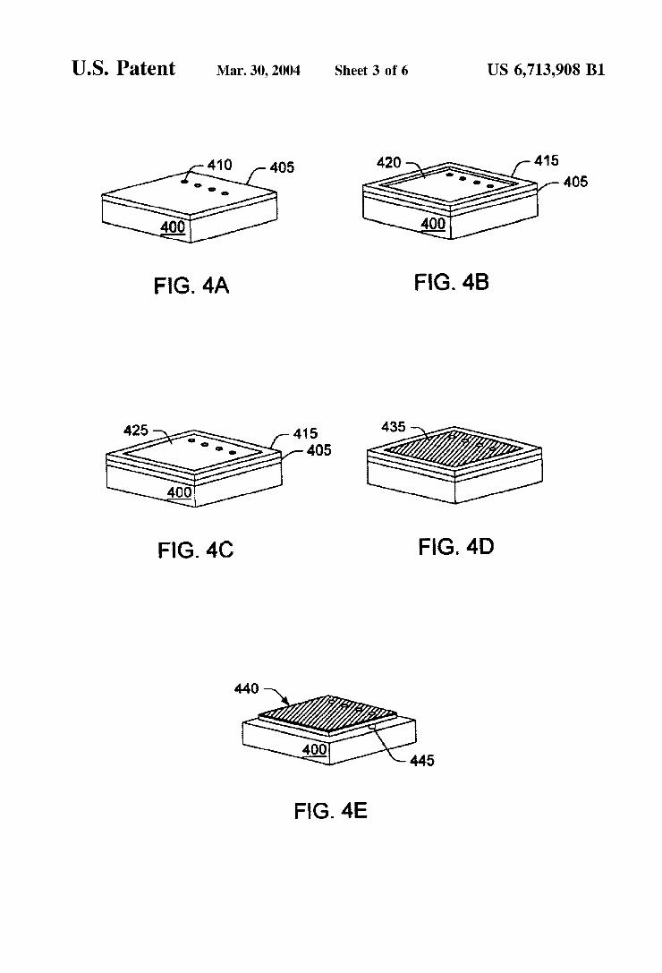
FIGS. 4Athrough 4E show one technique for creating the 3s the mechanical spring material. Single crystal silicon has magnetic actuation plate on a substrate 400. First, a sacri- strength properties similar to steel without the plastic defor- ficial spacing layer 405 is deposited onto the substrate 400 mation limitations. (FIG. 4A). The spacing layer 405 is formed from an etchable FIGS. 5A through 5C show the components of a switch material, such as photoresist. In highly miniaturized fabricated from three substrates. The first substrate 500 switches, the spacing layer 405 typically has a thickness of 40 (FIG. 5A) includes the magnetic actuation plate 515, which between 2 p m and 20pm. The spacing layer 405 is patterned is formed on the surface of or as a cantilevered beam 520 in to form anchor holes 410, which allow the magnetic material the substrate 500. Electrical contacts 525 are molded at the forming the actuation plate to bond with the substrate 400 as free end of the cantilevered beam 520. At least a portion of described below. In many switches, a very thin electroplat- the substrate 500 includes a conductive layer 535 that allows ing seed layer is deposited over the spacing layer to facilitate 4s electrical connection between the contact points at the end of formation of the magnetic actuation plate. the magnetic actuation plate 515 and at least a portion of the
A photoresist plating mold layer 415 then is deposited surrounding frame. In many switches, this conductive layer over the spacing layer 405 and patterned to form a mold 535 is the magnetic plate itself. Alternatively, the conductive cavity 420 (FIG. 4B). The mold cavity 420 exposes most of layer 535 is formed by depositing an electrical contact the spacing layer 405, including the anchor holes 410. A SO material, such as silver or gold, over the surface of the magnetic material 425, such as permalloy, is deposited onto substrate 500. Holes or recesses 530a-d are formed in the the spacing layer 405, filling the mold cavity 420 (FIG. 4C). substrate 500, including in the conductive area 535, to allow The magnetic material 425 also fills the anchor holes 410 in alignment and, in some cases, electrical contact with the the spacing layer 405, forming anchors (discussed below) other substrates. that contact the substrate 400 directly. The magnetic material ss The second substrate 505 (FIG. 5B) includes a conductive 425 is deposited to a thickness of between 10 pm and 20pm contact plate 540 that connects electrically to the magnetic in many highly miniaturized switches. actuation plate 515 only when the switch is active. The
Alayer of contact material 435 then is deposited over the contact plate 540 often is formed from the same material as layer of magnetic material 425 (FIG. 4D). The contact the electrical contacts 525 on the magnetic actuation plate material 435 is selected from a wide range of materials with 60 515, but other contact materials also are used. The second good electrical contact properties, including evaporated met- substrate 505 also includes spacers 545,550~-d that provide als such as gold and silver. A typical thickness for the contact the required physical separation between the magnetic layer 435 is between 0.1 pm and 10 pm. actuation plate 515 and the contact plate 540. The spacers
An etchant then is used to remove the photoresist mold 545, 550a-d can be formed in place from nearly any layer 415 and spacing layer 405 from the substrate 400, 65 material, either conductive or insulative. The spacers may leaving a magnetic actuation plate 440 mounted to the also be placed manually, if desired. One approach uses a substrate 400 by anchors 445. The magnetic actuation plate low-resistance conductive material, such as copper, that is
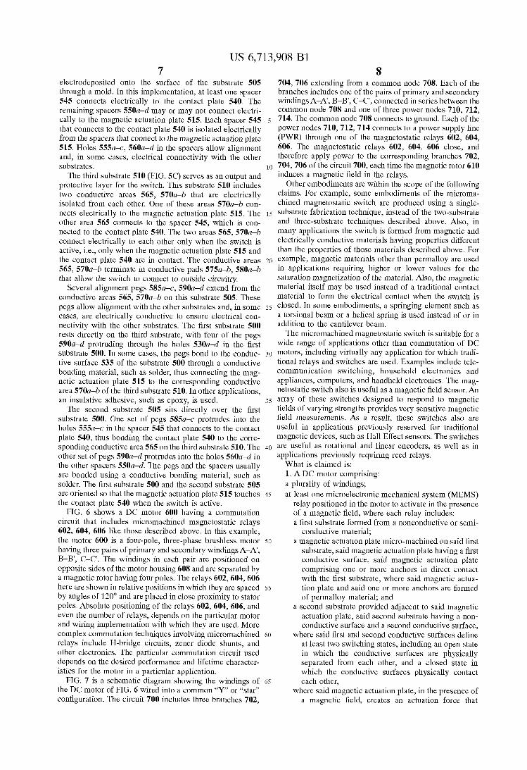
US 6,713,908 B1 7 8
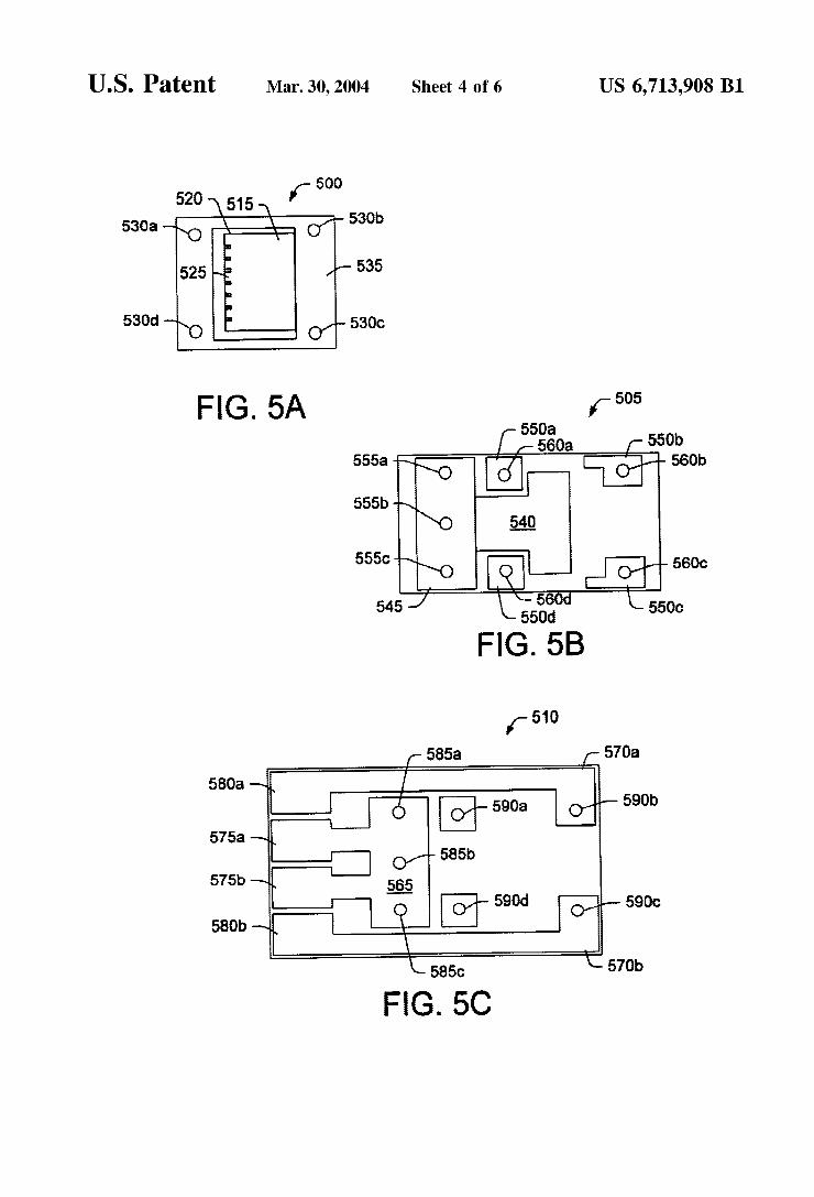
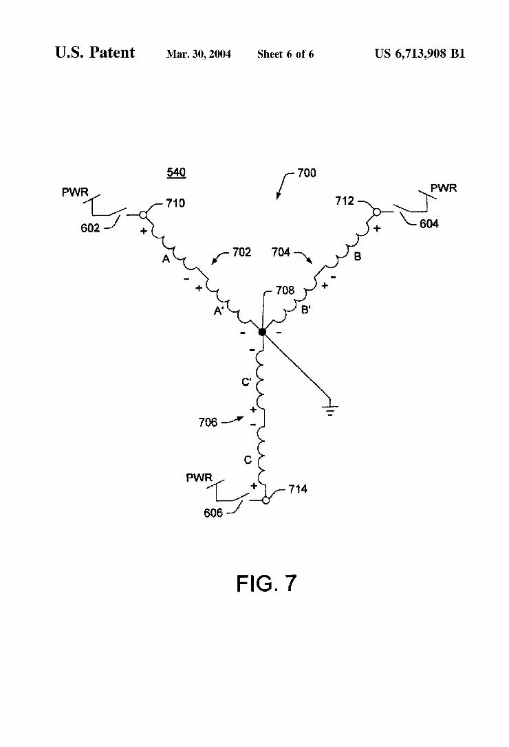
electrodeposited onto the surface of the substrate 505 704, 706 extending from a common node 708. Each of the through a mold. In this implementation, at least one spacer branches includes one of the pairs of primary and secondary 545 connects electrically to the contact plate 540. The windings A-A’, B-B’, C-C’, connected in series between the remaining spacers 550a-d may or may not connect electri- ~ ~ m m o n node 708 and one of three power nodes 710,712, cally to the magnetic actuation plate 515. Each spacer 545 s 714. The common node 708 connects to ground. Each of the that connects to the contact plate 540 is isolated electrically Power nodes 7102 712,714 connects to a Power Supply line from the spacers that connect to the magnetic actuation plate (PWR) through one of the magnetostatic relays 602, 604, 515. Holes 555a-c, 560a-d in the spacers allow alignment 606. The magnetostatic relays 602, 604, 606 close, and and, in some cases, electrical connectivity with the other therefore apply power to the corresponding branches 702, substrates. 704,706 of the circuit 700, each time the magnetic rotor 610
The third substrate 510 (FIG. 5C) serves as an output and induces a magnetic field in the relays. protective layer for the switch. This substrate 510 includes Other embodiments are within the scope ofthe following two conductive areas 565, 57oa-b that are electrically claims. For example, some embodiments of the microma- isolated from each other, One of these areas 570a-b con- chined magnetostatic switch are produced using a single- nects electrically to the magnetic actuation plate 515, The 1s substrate fabrication technique, instead of the two-substrate other area 565 connects to the spacer 545, which is con- and three-substrate techniques described above. Also, in nected to the contact plate 540. The two areas 565, 570a-b many applications the switch is formed from magnetic and connect electrically to each other only when the switch is electrically conductive materials having properties different active, i,e,, only when the magnetic actuation plate 515 and than the properties of those materials described above. For the contact plate 540 are in contact. The conductive areas 20 example, magnetic materials other than Permalloy are used 565, 57oa-b terminate in conductive pads 575a-b, 58Oa-b in applications requiring higher or lower values for the that allow the switch to connect to outside circuitry. saturation magnetization of the material. Also, the magnetic
Several alignment pegs 585a-~ , 590a-d extend from the material itself may be used instead of a traditional contact conductive areas 565, 570a-b on this substrate 505, These material to form the electrical contact when the switch is pegs allow alignment with the other substrates and, in some zs closed. In Some embodiments, a springing element such as cases, are electrically conductive to ensure electrical con- a torsional beam or a helical spring is used instead of or in nectivity with the other substrates. The first substrate 500 addition to the cantilever beam. rests directly on the third substrate, with four of the pegs The micromachined magnetostatic switch is suitable for a 590a-d protruding through the holes 5 3 0 ~ 4 in the first wide range of applications other than commutation of DC substrate 500. In some cases, the pegs bond to the conduc- 30 motors, including virtually any application for which tradi- tive surface 535 of the substrate 500 through a conductive tional relays and switches are used. Examples include tele- bonding material, such as solder, thus connecting the mag- communication switching, household electronics and netic actuation plate 515 to the corresponding conductive appliances, computers, and handheld electronics. The mag- area 57oa-b of the third substrate 510, In other applications, netostatic switch also is useful as a magnetic field sensor. An an insulative adhesive, such as epoxy, is used. 35 array of these switches designed to respond to magnetic
The second substrate 505 sits directly Over the first fields Of varying strengths provides very sensitive magnetic substrate 500. One set of pegs 5 8 ~ ~ ~ protrudes into the field measurements. As a result, these switches also are holes 555a-c in the spacer 545 that connects to the contact useful in applications previously reserved for traditional plate 540, thus bonding the contact plate 540 to the corre- magnetic devices, such as Hall Effect sensors. The switches sponding conductive area 565 on the third substrate 510. The 40 are useful as rotational and linear encoders, as well as in other set of pegs 590a-d protrudes into the holes 560a-d in applications Previously requiring reed relays. the other sp&rs 550a-d: The pegs and the spacers usually are bonded using a conductive bonding material, such as solder. The first substrate 500 and the second substrate 505 are oriented so that the magnetic actuation plate 515 touches 45 the contact plate 540 when the switch is active.
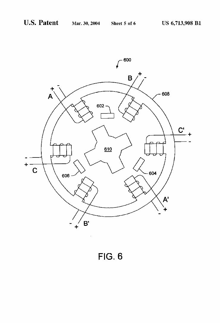
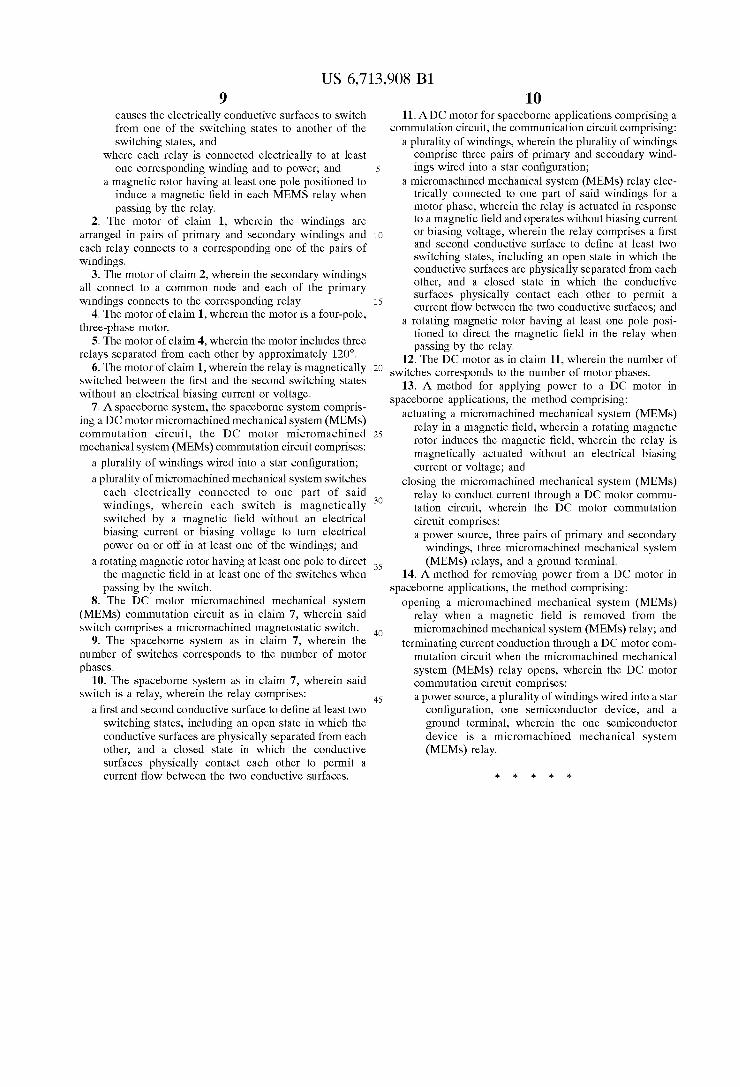
FIG. 6 shows a DC motor 600 having a commutation circuit that includes micromachined magnetostatic relays 602, 604, 606 like those described above. In this example, the motor 600 is a four-pole, three-phase brushless motor SO having three pairs of primary and secondary windings A-A‘, B-B’, C-C’. The windings in each pair are positioned on opposite sides of the motor housing 608 and are separated by a magnetic rotor having four poles. The relays 602,604,606 here are shown in relative positions in which they are spaced ss by angles of 120” and are placed in close proximity to stator poles. Absolute positioning of the relays 602, 604, 606, and even the number of relays, depends on the particular motor and wiring implementation with which they are used. More complex commutation techniques involving micromachined 60 relays include H-bridge circuits, zener diode shunts, and other electronics. The particular commutation circuit used depends on the desired performance and lifetime character- istics for the motor in a particular application.
the DC motor of FIG. 6 wired into a common “I”’ or “star” configuration. The circuit 700 includes three branches 702,
FIG. 7 is a schematic diagram showing the windings of 65
What is claimed is: 1. A DC motor comprising: a plurality of windings; at least one microelectronic mechanical system (MEMS)
relay positioned in the motor to activate in the presence of a magnetic field, where each relay includes: a first substrate formed from a nonconductive or semi-
conductive material; a magnetic actuation plate micro-machined on said first
substrate, said magnetic actuation plate having a first conductive surface, said magnetic actuation plate comprising one or more anchors in direct contact with the first substrate, where said magnetic actua- tion plate and said one or more anchors are formed of permalloy material; and
a second substrate provided adjacent to said magnetic actuation plate, said second substrate having a non- conductive surface and a second conductive surface,
where said first and second conductive surfaces define at least two switching states, including an open state in which the conductive surfaces are physically separated from each other, and a closed state in which the conductive surfaces physically contact each other,
where said magnetic actuation plate, in the presence of a magnetic field, creates an actuation force that
US 6,713,908 B1 9 10
causes the electrically conductive surfaces to switch 11. ADC motor for spaceborne applications comprising a from one of the switching states to another of the commutation circuit, the communication circuit comprising: switching states, and a plurality of windings, wherein the plurality of windings
where each relay is connected electrically to at least comprise three pairs of primary and secondary wind- one corresponding winding and to power; and ings wired into a star configuration;
a magnetic rotor having at least one pole positioned to a micromachined mechanical system (MEMs) relay elec- induce a magnetic field in each MEMS relay when trically connected to one part of said windings for a passing by the relay. motor phase, wherein the relay is actuated in response
2. The motor of claim 1, wherein the windings are to a magnetic field and operates without biasing current arranged in pairs of primary and secondary windings and IO Or biasing voltage, wherein the relay comprises a first each relay connects to a corresponding one of the pairs of and second conductive surface to define at least two windings. switching states, including an open state in which the
conductive surfaces are physically separated from each 3. The motor of claim 2, wherein the secondary windings other, and a closed state in which the conductive all connect to a common node and each of the primary surfaces physically contact each other to permit a current flow between the two conductive surfaces; and windings connects to the corresponding relay.
4. The motor of claim 1, wherein the motor is a four-pole, a rotating magnetic rotor having at least one pole posi- tioned to direct the magnetic field in the relay when three-phase motor. passing by the relay. 5. The motor of claim 4, wherein the motor includes three
12. The DC motor as in claim 11, wherein the number of relays separated from each other by approximately 120". 6. The motor of claim 1, wherein the relay is magnetically 20 switches corresponds to the number of motor phases,
switched between the first and the second switching states 13, A method for applying power to a DC motor in without an electrical biasing current or voltage. 7. A spaceborne system, the spaceborne system compris- actuating a micromachined mechanical system (MEMs) ing a DC motor micromachined mechanical system (MEMs) relay in a magnetic field, wherein a rotating magnetic commutation circuit, the DC motor micromachined zs rotor induces the magnetic field, wherein the relay is mechanical system (MEMs) commutation circuit comprises: magnetically actuated without an electrical biasing a plurality of windings wired into a star configuration; current or voltage; and a plurality of micromachined mechanical system switches closing the micromachined mechanical system ( M E M ~ )
each electrically connected to one part of said relay to conduct current through a DC motor commu- windings, wherein each switch is magnetically 30 tation circuit, wherein the DC motor commutation switched by a magnetic field without an electrical circuit comprises: biasing current or biasing voltage to turn electrical a power source, three pairs of primary and secondary power on or off in at least one of the windings; and windings, three micromachined mechanical system
a rotating magnetic rotor having at least one pole to direct 3s (MEMs) relays, and a ground terminal. the magnetic field in at least one of the switches when 14. A method for removing power from a DC motor in passing by the switch.
8. The DC motor micromachined mechanical system opening a micromachined mechanical system (MEMs) (MEMs) commutation circuit as in claim 7, wherein said relay when a magnetic field is removed from the switch comprises a micromachined magnetostatic switch. micromachined mechanical system (MEMs) relay; and
9. The spaceborne system as in claim 7, wherein the terminating current conduction through a DC motor com- number of switches corresponds to the number of motor mutation circuit when the micromachined mechanical phases. system (MEMs) relay opens, wherein the DC motor
10. The spaceborne system as in claim 7, wherein said commutation circuit comprises: switch is a relay, wherein the relay comprises: a power source, a plurality of windings wired into a star
a first and second conductive surface to define at least two configuration, one semiconductor device, and a switching states, including an open state in which the ground terminal, wherein the one semiconductor conductive surfaces are physically separated from each device is a micromachined mechanical system other, and a closed state in which the conductive (MEMs) relay. surfaces physically contact each other to permit a current flow between the two conductive surfaces.
5
Is
spaceborne applications, the method comprising:
spaceborne applications, the method comprising:
4o
45
* * * * *


![O… Les mots invariables - ekladata.comekladata.com/Xy4ZlndeM_21kbehZF21Y59e6fA/Lecons... · O… Le son [ill] Leson[ill]peuts’écriredeplusieursfaçons: i y il ille la bruyère](https://img.pdfslide.fr/doc/110x75/5b957d5009d3f272648caec7/o-les-mots-invariables-o-le-son-ill-lesonillpeutsecriredeplusieursfacons.jpg)