Embed Size (px)
Citation preview
®
ICEM, un outil pour la modélisation CEM des Circuits Intégrés
®
Jean-luc LEVANT
Expert CEM composantsMembre de l’UTE, groupe de normalisation CEM des
composants.
* ATMEL Nantes ( [email protected])
_ Jluc LEVANT / Atmel
® Content
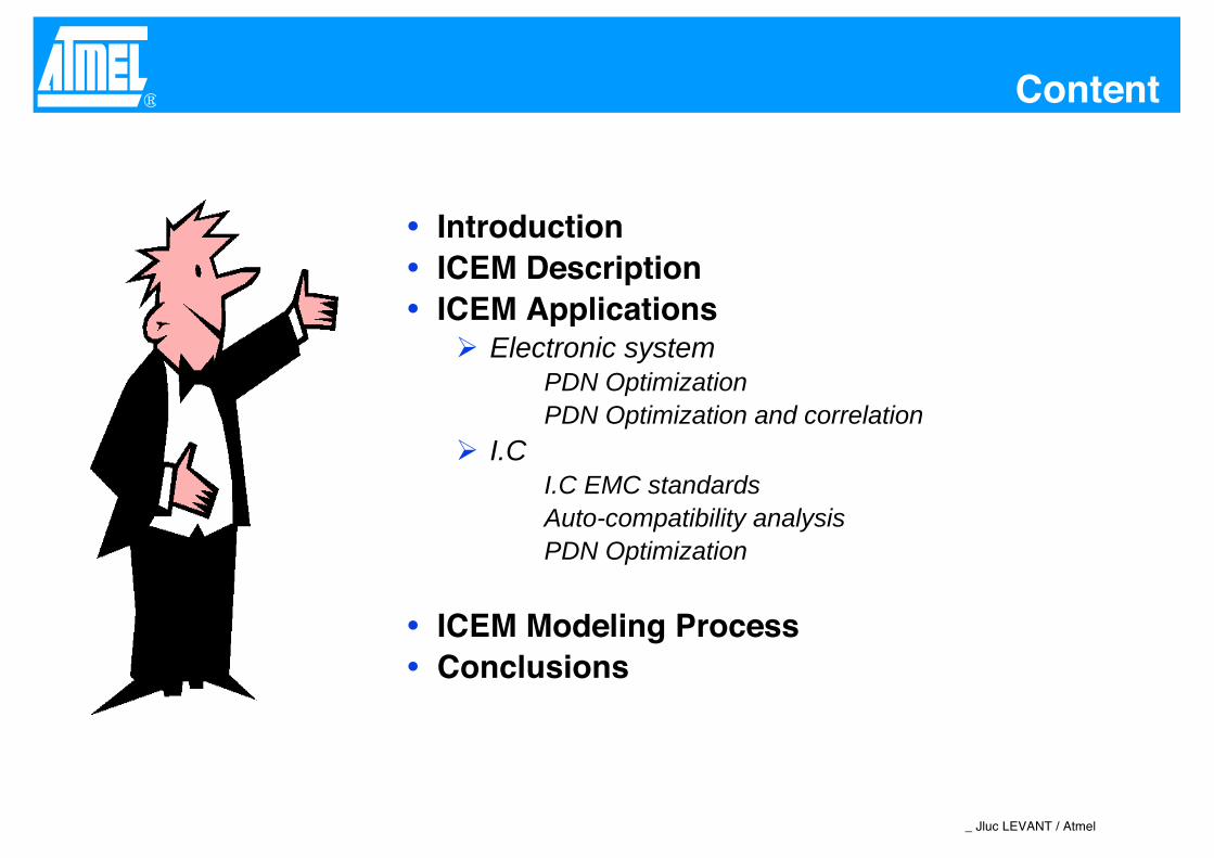
IntroductionICEM DescriptionICEM Applications
Electronic systemPDN OptimizationPDN Optimization and correlation
I.CI.C EMC standardsAuto-compatibility analysisPDN Optimization
ICEM Modeling ProcessConclusions

_ Jluc LEVANT / Atmel
®
Introduction
_ Jluc LEVANT / Atmel
® Introduction
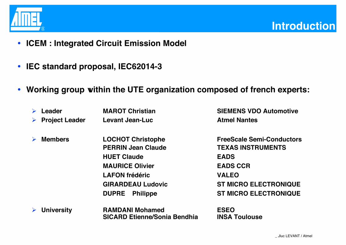
ICEM : Integrated Circuit Emission Model
IEC standard proposal, IEC62014-3
Working group within the UTE organization composed of french experts:
Leader MAROT Christian SIEMENS VDO AutomotiveProject Leader Levant Jean-Luc Atmel Nantes
Members LOCHOT Christophe FreeScale Semi-ConductorsPERRIN Jean Claude TEXAS INSTRUMENTSHUET Claude EADSMAURICE Olivier EADS CCRLAFON frédéric VALEOGIRARDEAU Ludovic ST MICRO ELECTRONIQUEDUPRE Philippe ST MICRO ELECTRONIQUE
University RAMDANI Mohamed ESEOSICARD Etienne/Sonia Bendhia INSA Toulouse
_ Jluc LEVANT / Atmel
® Introduction
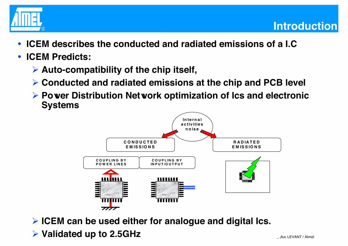
ICEM describes the conducted and radiated emissions of a I.CICEM Predicts:
Auto-compatibility of the chip itself,Conducted and radiated emissions at the chip and PCB levelPower Distribution Network optimization of Ics and electronic Systems
ICEM can be used either for analogue and digital Ics.Validated up to 2.5GHz
In te rn a la c tiv it ie s
n o is e
C O N D U C T E DE M IS S IO N S
R A D IA T E DE M IS S IO N S
C O U P L IN G B YP O W E R L IN E S
A L IM E N T A T IO N S
C O U P L IN G B YIN P U T /O U T P U T
A L IM E N T A T IO N S
_ Jluc LEVANT / Atmel
®
ICEM Model description
_ Jluc LEVANT / Atmel
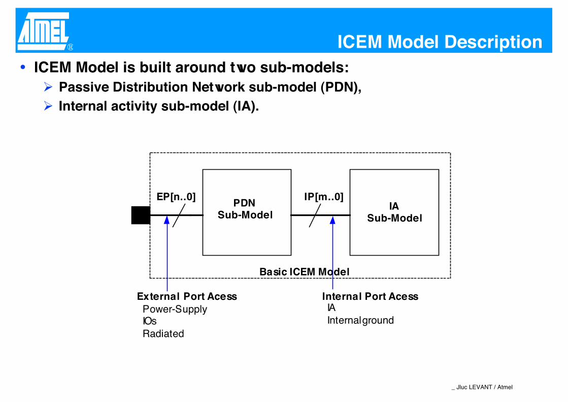
® ICEM Model DescriptionICEM Model is built around two sub-models:
Passive Distribution Network sub-model (PDN),Internal activity sub-model (IA).
PDNSub-Model
IASub-Model
EP[n..0] IP[m..0]
Basic ICEM Model
External Port Acess Internal Port AcessIAInternal ground
Power-SupplyIOsRadiated
_ Jluc LEVANT / Atmel
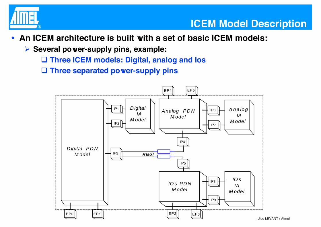
® ICEM Model DescriptionAn ICEM architecture is built with a set of basic ICEM models:
Several power-supply pins, example:Three ICEM models: Digital, analog and IosThree separated power-supply pins
RIsol
Analog PD NM odel
IO s IC EMM odel
D igital PD NM odel
IO s PD NM odel
D igital IA
M odel
A n a lo g IA
M odel
IO sIA
M odel
EP0 EP1 EP2 EP3
EP4 EP5
IP1
IP2
IP3
IP4
IP5
IP6
IP7
IP8
IP9
_ Jluc LEVANT / Atmel
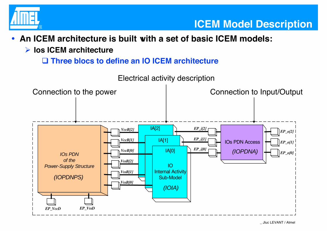
® ICEM Model DescriptionAn ICEM architecture is built with a set of basic ICEM models:
Ios ICEM architectureThree blocs to define an IO ICEM architecture
Electrical activity description
Connection to the power Connection to Input/Output
VccB[0]
EP_VccD EP_VssD
IOs PDNof the
Power-Supply Structure
VccB[2]
VccB[1]
VssB[2]
VssB[1]
VssB[0]
IA[2]
IA[1]
EP_o[2]
EP_o[1]
EP_o[0]
IOs PDN AccessEP_i[0]
EP_i[2]
EP_i[1]
(IOPDNPS)
(IOPDNA)IA[0]
IOInternal Activity
Sub-Model
(IOIA)
_ Jluc LEVANT / Atmel
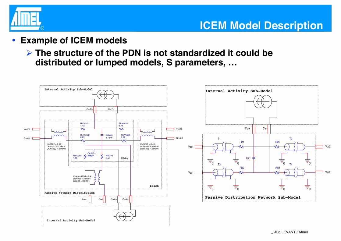
® ICEM Model DescriptionExample of ICEM models
The structure of the PDN is not standardized it could be distributed or lumped models, S parameters, …
T1 T2Ric1 Ric2
Ric3 Ric4
Cic1
T4T3 0 0
00
0
0
0
0
Vss1
Vcc1
Vss2
Vcc2
Cur-Cur+
Passive Distribution Network Sub-Model
Internal Activity Sub-Model
Passive Network Distribution
CurA+ CurA-
ZPack
ZDie
Internal Activity Sub-Model
Internal Activity Sub-Model
Kic2122 = 0.49LicVcc21 = 3.98nHLiCVss22 = 3.98nH
Kic5253 = 0.49LicVcc52 = 3.98nHLicVss53 = 3.98nH
KicAVccGNd = 0.41LicAVcc = 3.98nHLicGnd = 3.98nH
RicVcc211.43
RicVcc520.79
RicVss220.85
RicVss530.62
RicGnd0.47
RicAVcc1.66
CicVcc3.15nF
CicAVcc388pF
Gnd63
Vcc52
GndAvcc
Gnd22
Vcc21
CurD-CurD+
_ Jluc LEVANT / Atmel
® ICEM Model Description
VccIOPDN VccCorePDN
VssCorePDNVssIOPDN
IoIA + CoreIA +
Risol1 10IO_IA - CoreIA -
LicB1 3.56n
Cicb1 851pfCic1 6.2n
Ricb1 1.7
SIA_IOs
SIA_Core
Lic1 5.66n
Ric1 1.7
IO PDNIO IA Core PDN Core IA
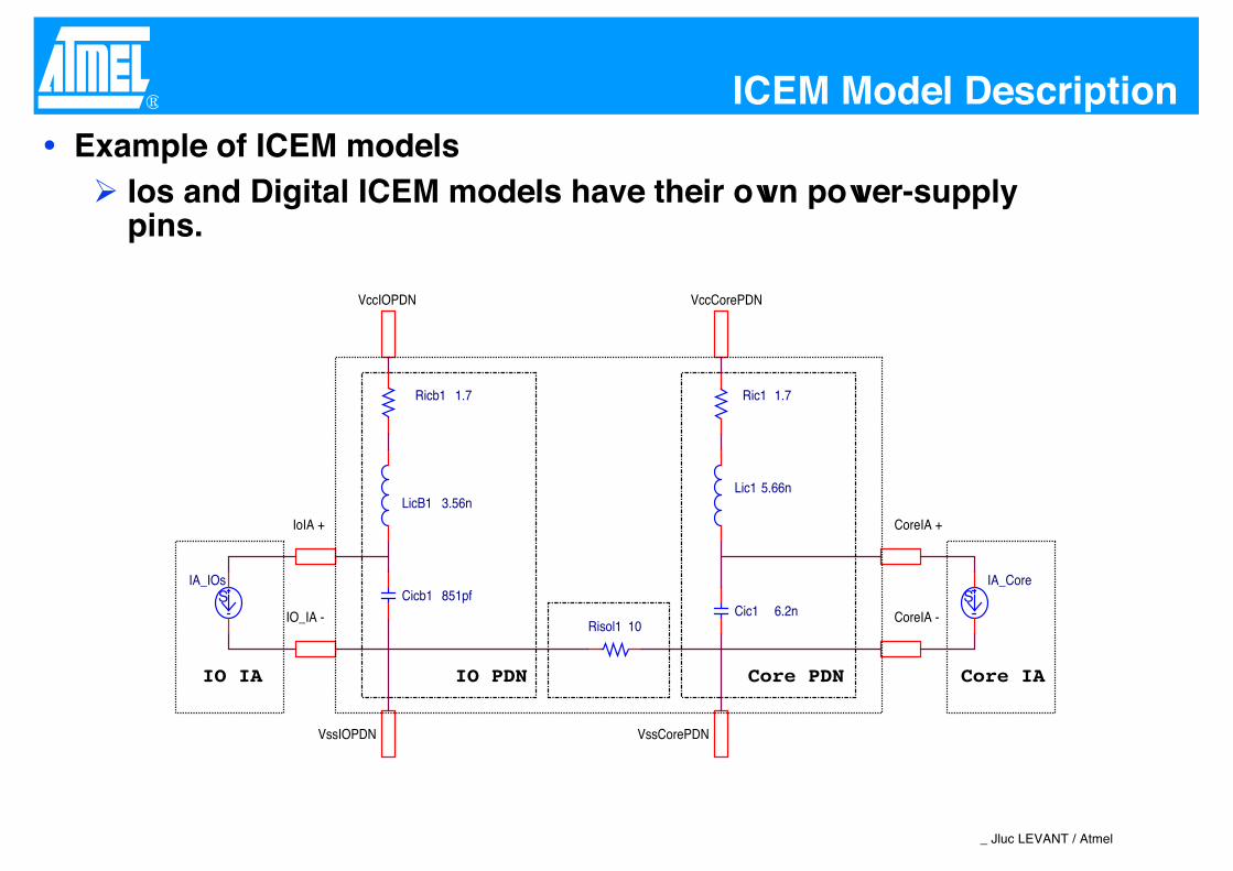
Example of ICEM modelsIos and Digital ICEM models have their own power-supply pins.
_ Jluc LEVANT / Atmel
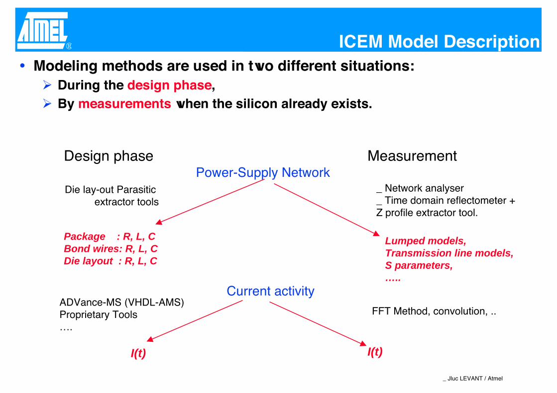
® ICEM Model DescriptionModeling methods are used in two different situations:
During the design phase,By measurements when the silicon already exists.
MeasurementPower-Supply Network
Design phase
Package : R, L, CBond wires: R, L, CDie layout : R, L, C
_ Network analyser_ Time domain reflectometer +Z profile extractor tool.
Die lay-out Parasitic extractor tools
Lumped models,Transmission line models,S parameters,…..
Current activityADVance-MS (VHDL-AMS)Proprietary Tools….
FFT Method, convolution, ..
I(t)I(t)
_ Jluc LEVANT / Atmel
®
ICEM Applications
_ Jluc LEVANT / Atmel
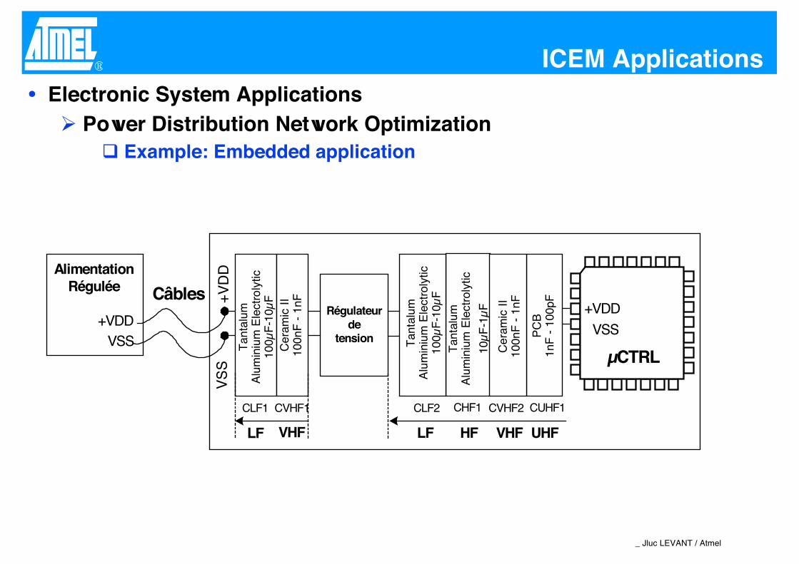
® ICEM ApplicationsElectronic System Applications
Power Distribution Network OptimizationExample: Embedded application
+VDD
VSS
AlimentationRégulée
+VDD
+V
DD
VS
S
VSS Tan
talu
mA
lum
iniu
m E
lect
roly
tic10
0µF
-10µ
F
µCTRLCer
amic
II
100n
F -
1nF
Tan
talu
mA
lum
iniu
m E
lect
roly
tic
10µ
F-1
µF
PC
B1n
F -
100
pF
Câbles
LF UHFVHFHF
CHF1 CVHF2 CUHF1
Régulateurde
tension Tan
talu
mA
lum
iniu
m E
lect
roly
tic10
0µF
-10µ
F
CLF2
LF
Cer
amic
II
100n
F -
1nF
CVHF1CLF1
VHF
_ Jluc LEVANT / Atmel
® ICEM Applications
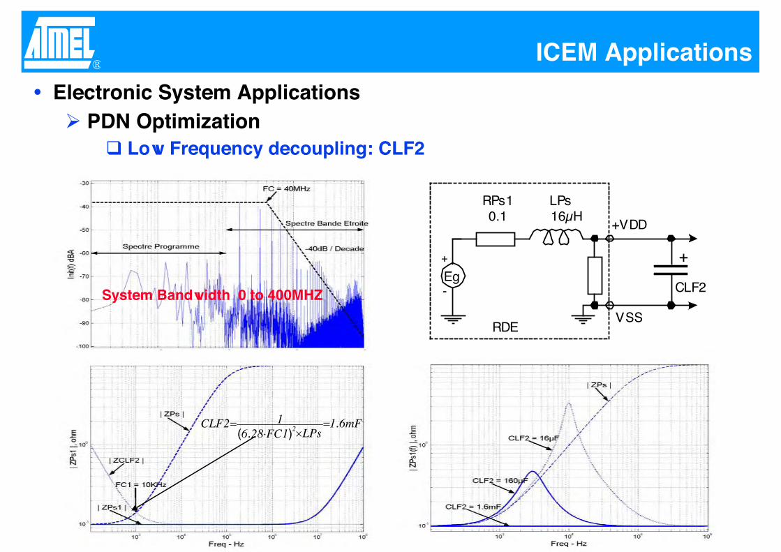
0.5 1 1.5 2 2.5 3 3.5 4
x 10-6
4
6
8
10
12
14
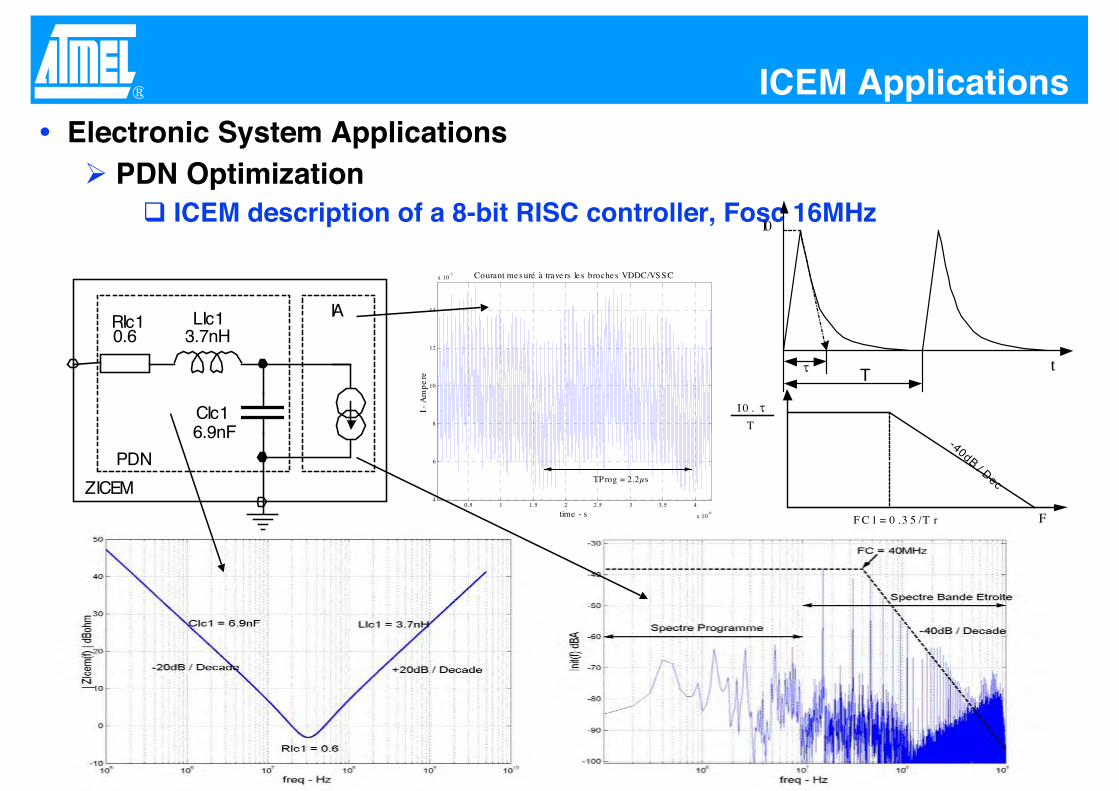
x 10-3 Courant me s uré à trave rs le s broche s VDDC/VS S C
time - s
I - A
mp
ere
TP rog = 2.2µs
Electronic System ApplicationsPDN Optimization
ICEM description of a 8-bit RISC controller, Fosc 16MHz
RIc1 LIc1
CIc1
0.6 3.7nH
6.9nF
ZICEM
PDN
IA
I0
tT
F C 1 = 0 .3 5 / T r
T
I 0 .
-40dB/ Dec
F
_ Jluc LEVANT / Atmel
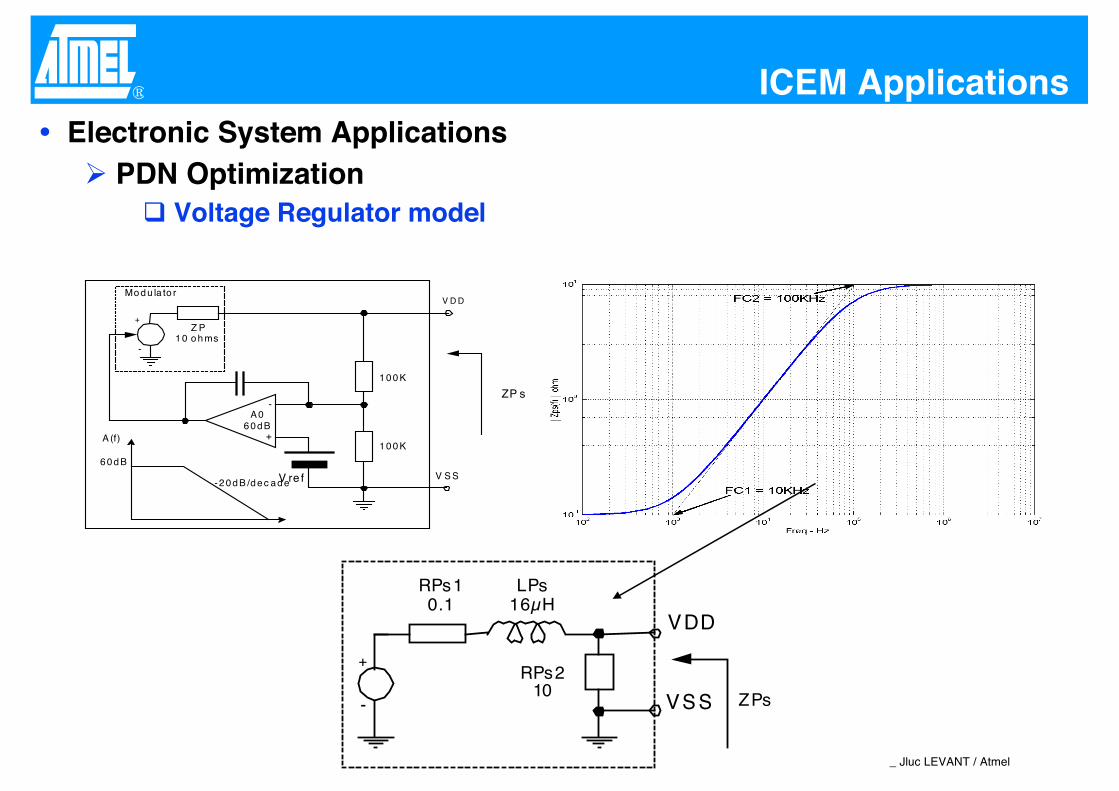
® ICEM ApplicationsElectronic System Applications
PDN Optimization Voltage Regulator model
-
+
+
-
Z P1 0 o h ms
Mo d u la to r
1 0 0 K
1 0 0 K
V D D
V S S
ZP s
V re f
A 06 0 d B
6 0 d B
A (f)
-2 0 d B /d e c a d e
+
-
LPsRPs1
RPs2
VDD
VSS
0.1
10
16µH
ZPs
_ Jluc LEVANT / Atmel
®ICEM Applications
Electronic System ApplicationsPDN Optimization
Low Frequency decoupling: CLF2
+
-
LPsRPs1
+VDD
VSS
0.1 16µH
CLF2
RDE
Eg
+
mF61LPs1FC286
12CLF 2 .).(
System Bandwidth 0 to 400MHZ
_ Jluc LEVANT / Atmel
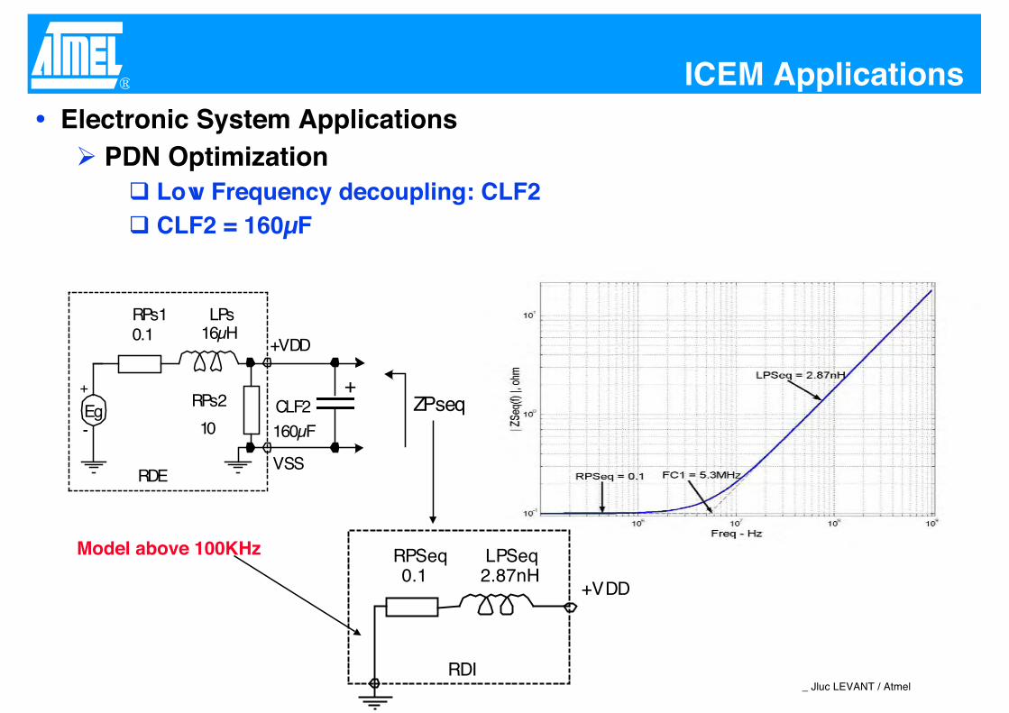
® ICEM ApplicationsElectronic System Applications
PDN Optimization Low Frequency decoupling: CLF2CLF2 = 160µF
+
-
LPsRPs1
+VDD
VSS
0.1 16µH
CLF2
RDE
Eg
+ZPseq
160µF10
RPs2
LPSeqRPSeq0.1 2.87nH
RDI
+VDD
Model above 100KHz
_ Jluc LEVANT / Atmel
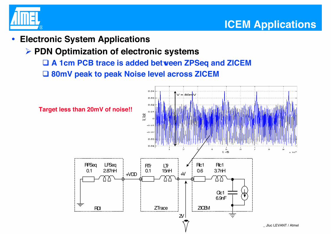
® ICEM ApplicationsElectronic System Applications
PDN Optimization of electronic systemsA 1cm PCB trace is added between ZPSeq and ZICEM80mV peak to peak Noise level across ZICEM
LPSeqRPSeq
+VDD0.1 2.87nH
RDI
LTrRTr0.1 15nH
RIc1 RIc1
CIc1
0.6 3.7nH
6.9nF
ZICEMZTrace
+V
ZV
Target less than 20mV of noise!!
_ Jluc LEVANT / Atmel
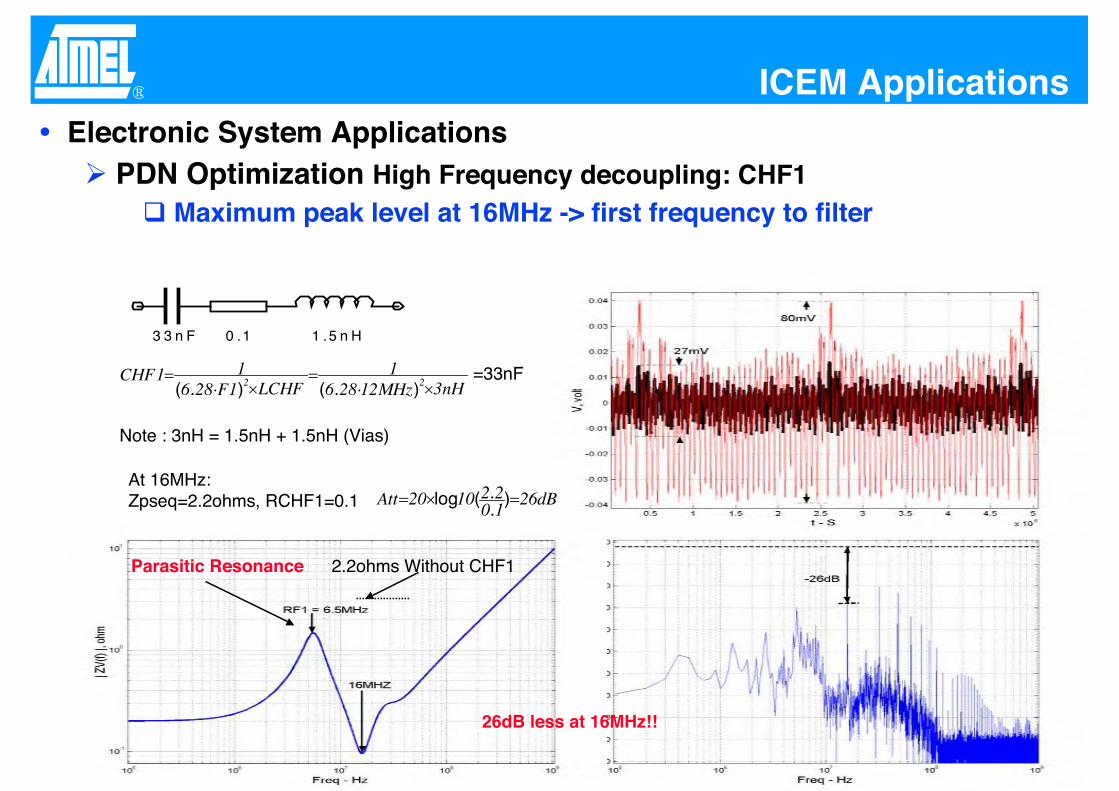
® ICEM ApplicationsElectronic System Applications
PDN Optimization High Frequency decoupling: CHF1Maximum peak level at 16MHz -> first frequency to filter
nH3MHz122861
LCHF1F28611CHF 22 ).().(
=33nF
Note : 3nH = 1.5nH + 1.5nH (Vias)
3 3 n F 0 .1 1 .5 n H
dB2610221020Att )..(log
At 16MHz:Zpseq=2.2ohms, RCHF1=0.1
Parasitic Resonance 2.2ohms Without CHF1
26dB less at 16MHz!!
_ Jluc LEVANT / Atmel
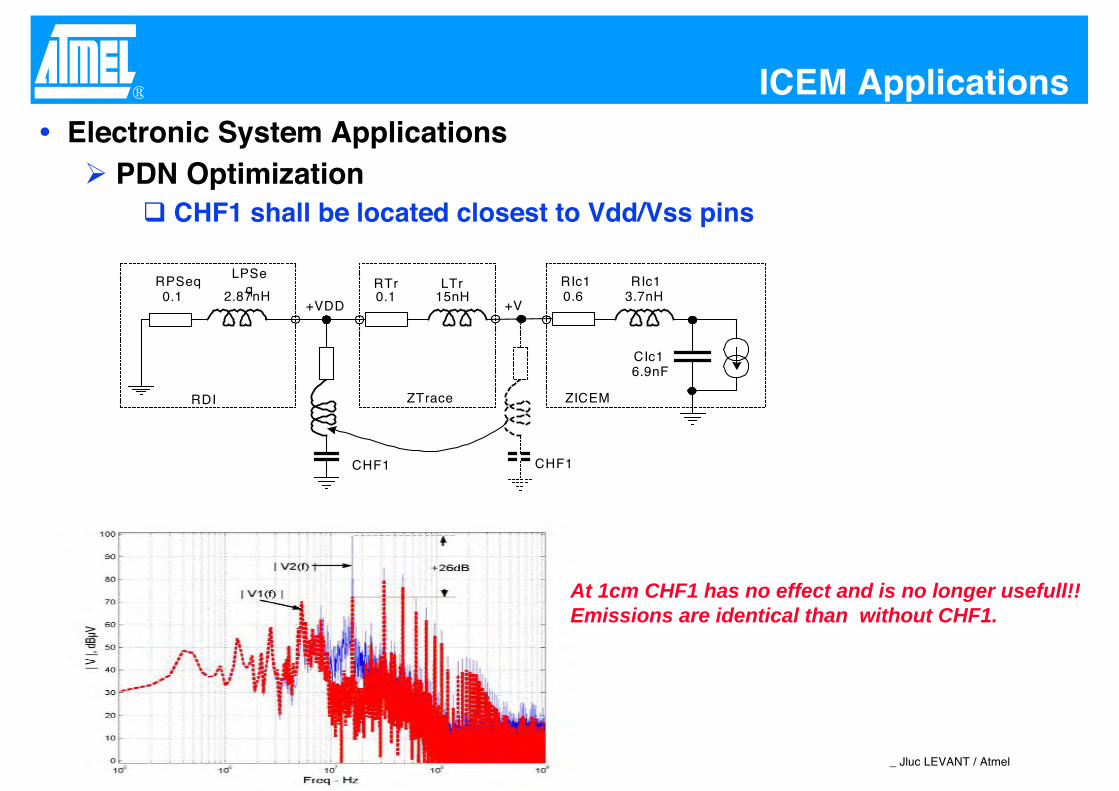
® ICEM ApplicationsElectronic System Applications
PDN Optimization CHF1 shall be located closest to Vdd/Vss pins
LPSeq
RPSeq
+VDD0.1 2.87nH
RDI
LTrRTr0.1 15nH
RIc1 RIc1
CIc1
0.6 3.7nH
6.9nF
ZICEMZTrace
+V
CHF1 CHF1
At 1cm CHF1 has no effect and is no longer usefull!!Emissions are identical than without CHF1.
_ Jluc LEVANT / Atmel
® ICEM Applications
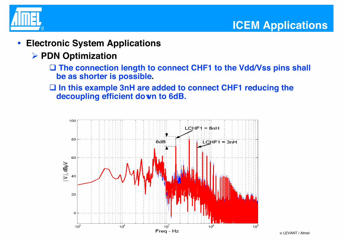
Electronic System ApplicationsPDN Optimization
The connection length to connect CHF1 to the Vdd/Vss pins shall be as shorter is possible.In this example 3nH are added to connect CHF1 reducing the
decoupling efficient down to 6dB.
_ Jluc LEVANT / Atmel
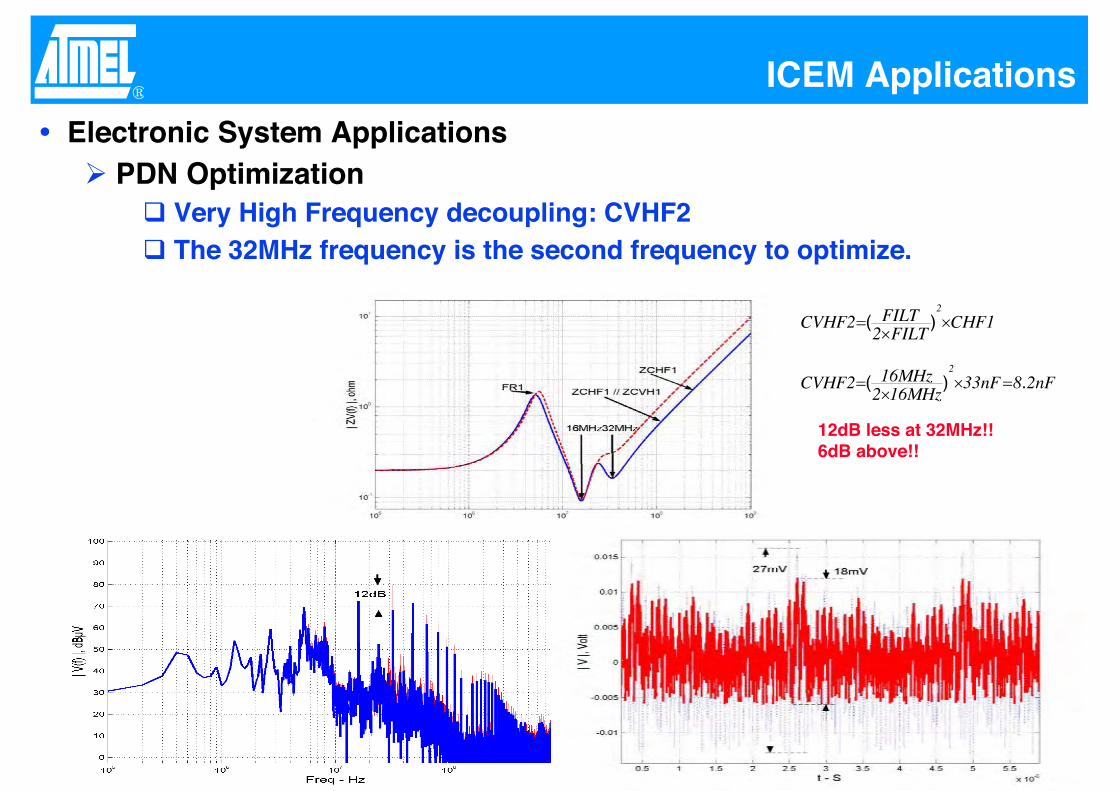
®ICEM Applications
Electronic System ApplicationsPDN Optimization
Very High Frequency decoupling: CVHF2The 32MHz frequency is the second frequency to optimize.
1CHFFILT2FILT2CVHF
2
)(
nF28nF33MHz162MHz162CVHF
2
.)(
12dB less at 32MHz!!6dB above!!
_ Jluc LEVANT / Atmel
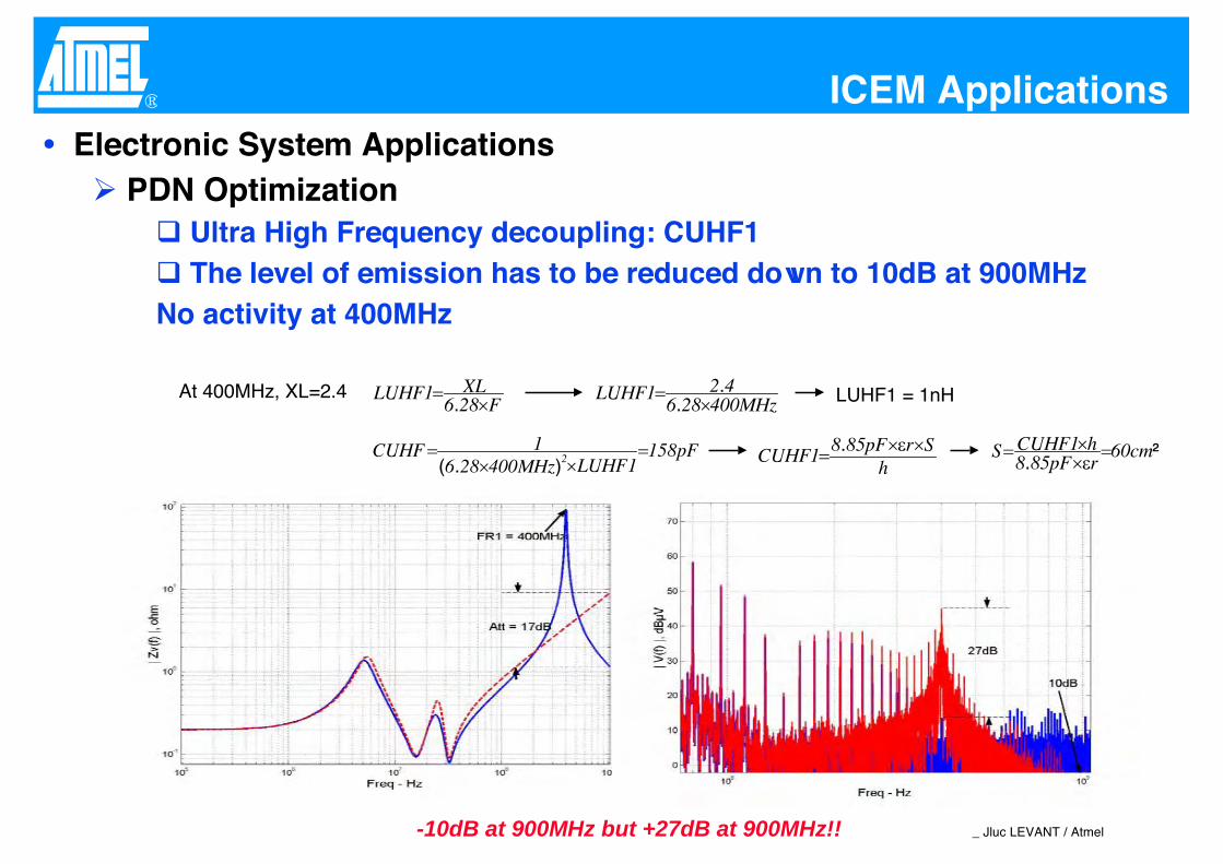
® ICEM ApplicationsElectronic System Applications
PDN OptimizationUltra High Frequency decoupling: CUHF1The level of emission has to be reduced down to 10dB at 900MHz
No activity at 400MHz
F286XL1LUHF
. MHz400286421LUHF
..At 400MHz, XL=2.4 LUHF1 = 1nH
hSrpF858
1CUHF.pF158
1LUHFMHz4002861CUHF 2).(
².
cm60rpF858h1CUHFS
².
cm60rpF858h1CUHFS
-10dB at 900MHz but +27dB at 900MHz!!
_ Jluc LEVANT / Atmel
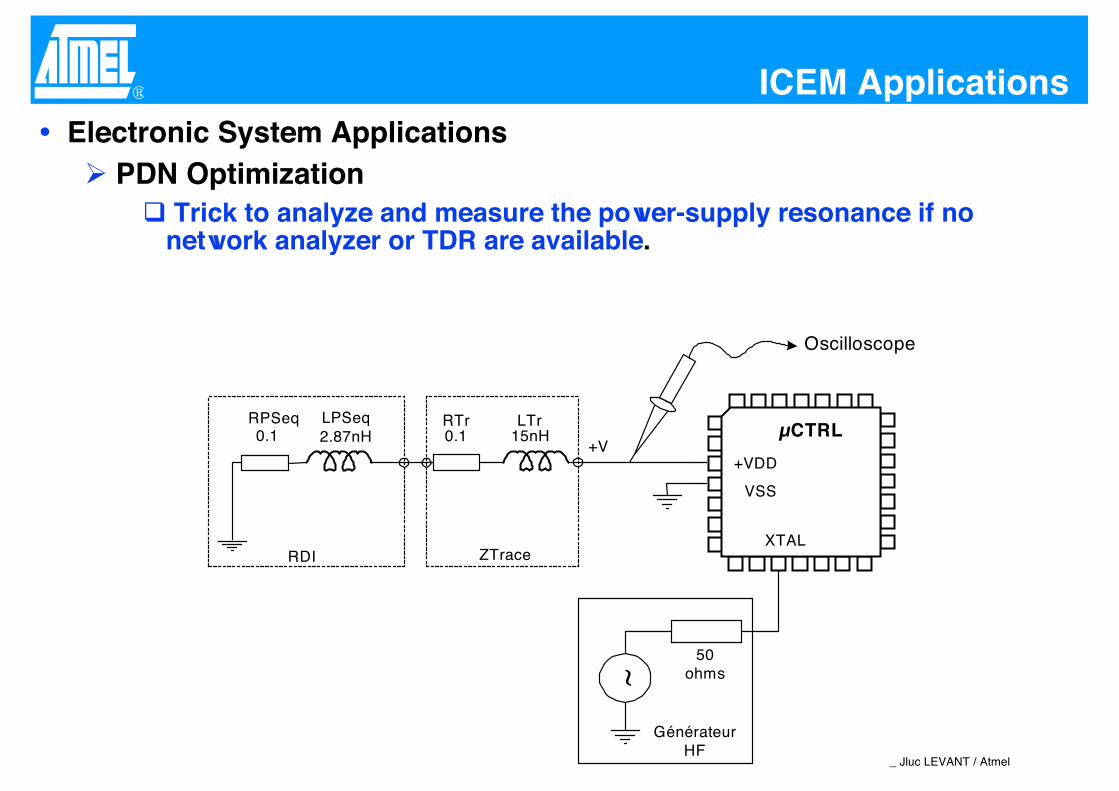
® ICEM ApplicationsElectronic System Applications
PDN OptimizationTrick to analyze and measure the power-supply resonance if no
network analyzer or TDR are available.
LPSeqRPSeq0.1 2.87nH
RDI
LTrRTr0.1 15nH
ZTrace
+V+VDD
VSS
µCTRL
XTAL
~
GénérateurHF
50ohms
Oscilloscope
_ Jluc LEVANT / Atmel
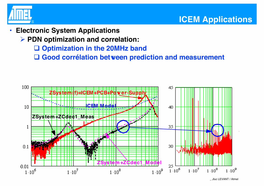
® ICEM Applications• Electronic System Applications
PDN optimization and correlation:Optimization in the 20MHz bandGood corrélation between prediction and measurement
ICEM Model
ZSystem (f)=ICEM+PCB+Pow er-Supply
ZSystem +ZCdec1_Meas
ZSystem +ZCdec1_Model
_ Jluc LEVANT / Atmel
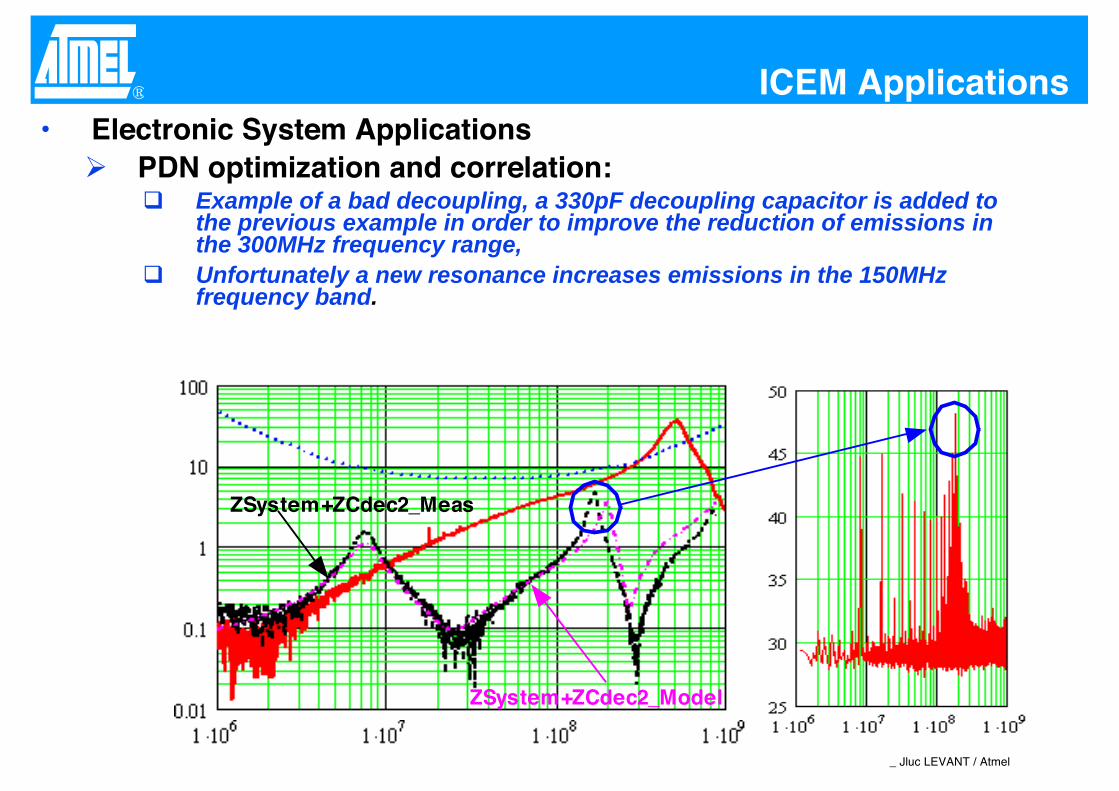
® ICEM Applications• Electronic System Applications
PDN optimization and correlation:Example of a bad decoupling, a 330pF decoupling capacitor is added to the previous example in order to improve the reduction of emissions in the 300MHz frequency range,Unfortunately a new resonance increases emissions in the 150MHz frequency band.
ZSystem+ZCdec2_Model
ZSystem+ZCdec2_Meas
_ Jluc LEVANT / Atmel
® ICEM Applications• Electronic System Applications
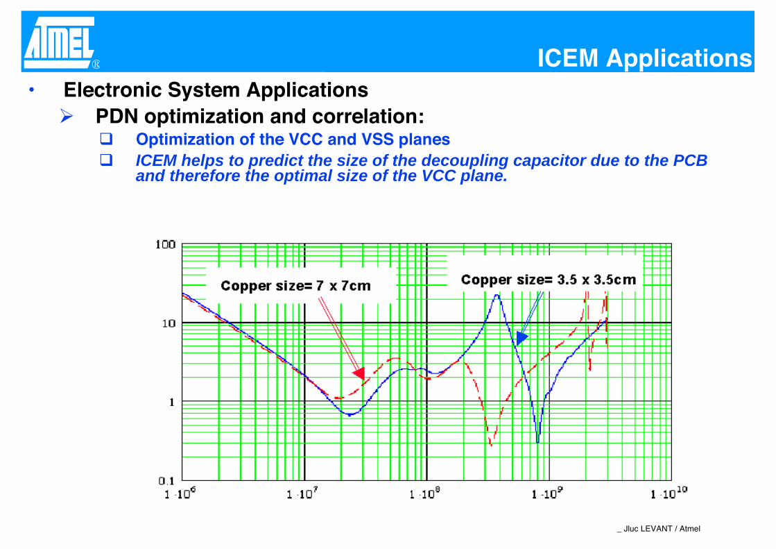
PDN optimization and correlation:Optimization of the VCC and VSS planesICEM helps to predict the size of the decoupling capacitor due to the PCB and therefore the optimal size of the VCC plane.
_ Jluc LEVANT / Atmel
® ICEM Applications• Electronic System Applications
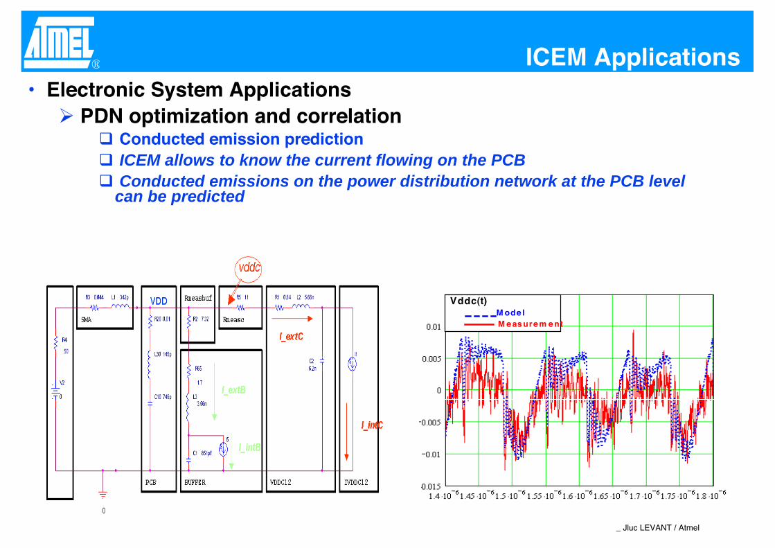
PDN optimization and correlationConducted emission predictionICEM allows to know the current flowing on the PCBConducted emissions on the power distribution network at the PCB levelcan be predicted
Vddc(t)M ode lM e as ure m e nt
_ Jluc LEVANT / Atmel
®ICEM Applications
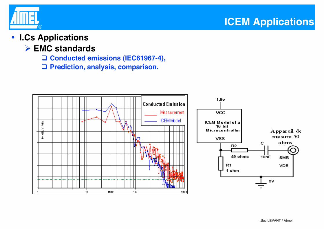
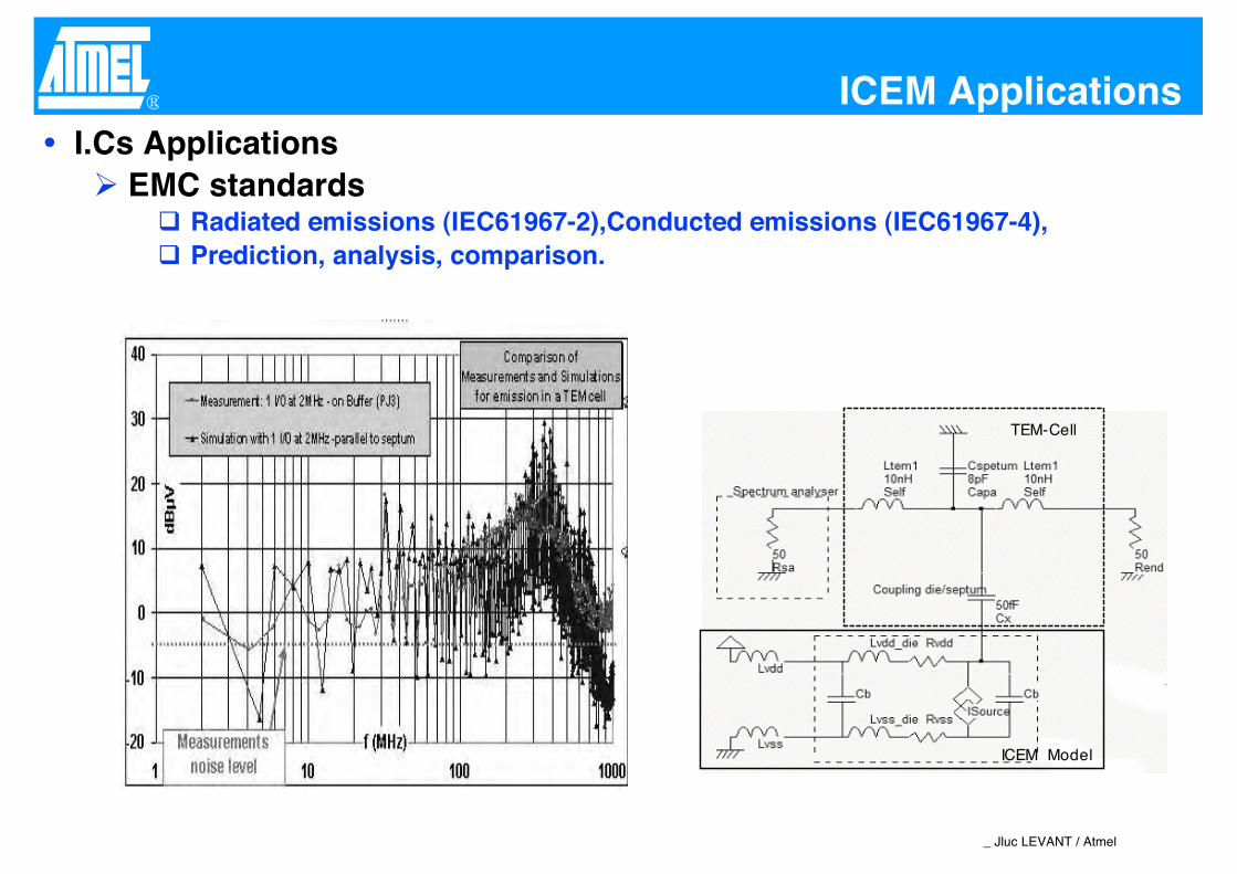
I.Cs ApplicationsEMC standards
Conducted emissions (IEC61967-4),Prediction, analysis, comparison.
_ Jluc LEVANT / Atmel
® ICEM ApplicationsI.Cs Applications
EMC standardsRadiated emissions (IEC61967-2),Conducted emissions (IEC61967-4),Prediction, analysis, comparison.
TEM-Cell
ICEM Model
_ Jluc LEVANT / Atmel
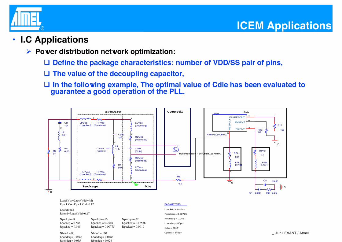
® ICEM Applications• I.C Applications
Power distribution network optimization:
Define the package characteristics: number of VDD/SS pair of pins,
The value of the decoupling capacitor,
In the following example, The optimal value of Cdie has been evaluated to guarantee a good operation of the PLL.
R3 2.2kC1 0.33n
PARAMETERS:
Lpackeq = 0.25nH
Rpackeq = 0.00775
Rbondeq = 0.055
Lbondeq = 80pH
Cdie = 50nF
Cpack = 816pF
Cdec1pf
L11nh
1
2
R10.01
C5 15pF
Npackpin=8Lpackeq = 0.5nh Rpackeq = 0.015
LpackVss=LapckVdd=4nhRpackVss=RpackVdd=0.12
R20.1
U29
ATMPLL500MHZ
CLKOUT0
CLKREFOUT1
RCFILT2
VS
SP
LL
13
0
CURMod1ZPNCore
DiePackage
RPLL
0.2
LPLL2.7nH
1
2
RPFilt
0.2
LPFilt2.7nH
1
2
R12
1GR131G
LPVcc{Lpackeq}
1 2
LPVss{Lpackeq}
1 2
LDVcc{Lbondeq}
1
2
LDVss{Lbondeq}
1
2
RPVcc{Rpackeq}
RPVss{Rpackeq}
RDVcc{Rbondeq}
RDVss{Rbondeq}
CDie{Cdie}
CPack{Cpack}
0
PLL
Ra
6.2
0
0
Npackpin=16Lpackeq = 0.25nh Rpackeq = 0.00775
Lbond=2nhRbond=RpackVdd=0.17
Npackpin=32Lpackeq = 0.125nh Rpackeq = 0.0019
Nbond = 80Lbondeq = 0.08nh Rbondeq = 0.055
Nbond = 160Lbondeq = 0.04nh Rbondeq = 0.028
C21pf
L21nH
1
2
R40.03
SI1
Implementation = DFCRB1_58KRHA
V
_ Jluc LEVANT / Atmel
® ICEM Applications
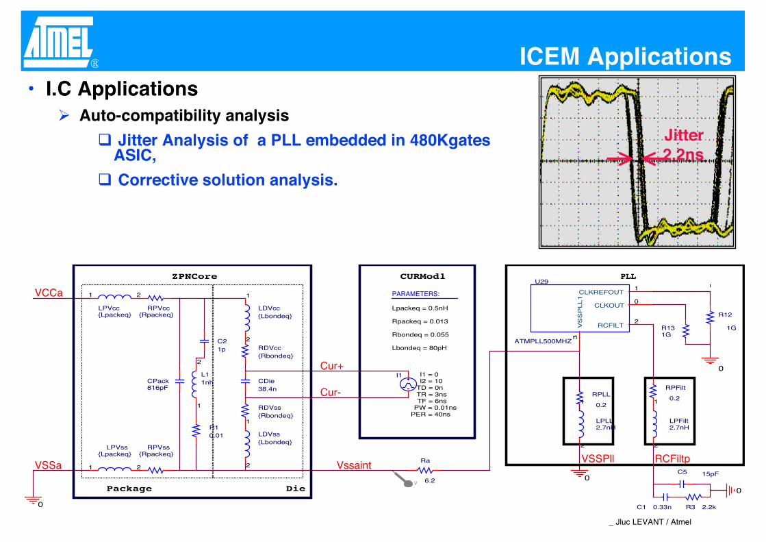
Jitter2.2ns
• I.C ApplicationsAuto-compatibility analysis
Jitter Analysis of a PLL embedded in 480KgatesASIC,
Corrective solution analysis.
R3 2.2kC1 0.33n
PARAMETERS:
Lpackeq = 0.5nH
Rpackeq = 0.013
Rbondeq = 0.055
Lbondeq = 80pHC21p
L11nh
1
2
R10.01
C5 15pF
V
U29
ATMPLL500MHZ
CLKOUT0
CLKREFOUT1
RCFILT2
VS
SP
LL
13
0
VSSa
VCCa
Cur+
Vssaint
CURMod1ZPNCore
DiePackage
LPLL2.7nH
1
2
RPLL
0.2
LPFilt2.7nH
1
2
RPFilt
0.2
R131G
R12
1G
LPVcc{Lpackeq}
1 2
LPVss{Lpackeq}
1 2
LDVcc{Lbondeq}
1
2
LDVss{Lbondeq}
1
2
RPVcc{Rpackeq}
RPVss{Rpackeq}
RDVcc{Rbondeq}
RDVss{Rbondeq}
CDie38.4n
CPack816pF
0
I1
TD = 0n
TF = 6nsPW = 0.01ns
PER = 40ns
I1 = 0I2 = 10
TR = 3ns
VSSPllRa
6.2
PLL
RCFiltp
0
Cur-
0
_ Jluc LEVANT / Atmel
®
ICEM Modeling Process
_ Jluc LEVANT / Atmel
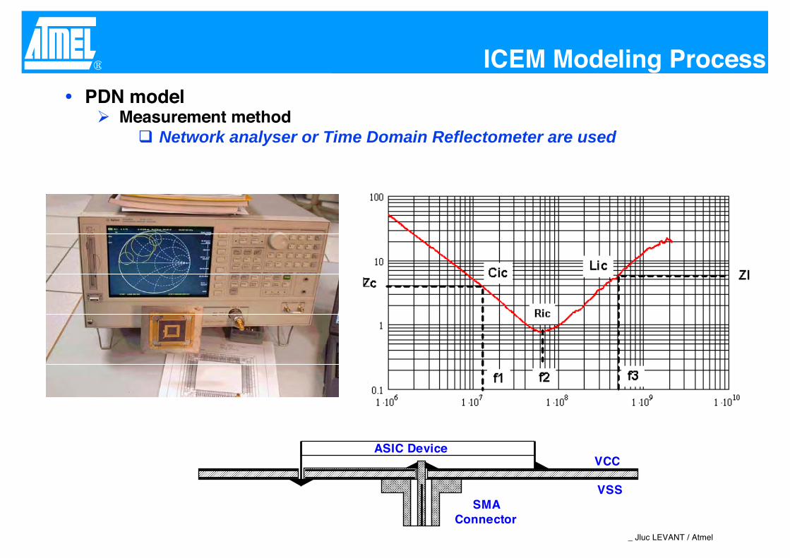
® ICEM Modeling ProcessPDN model
Measurement methodNetwork analyser or Time Domain Reflectometer are used
VCC
VSSSMA
Connector
ASIC Device
_ Jluc LEVANT / Atmel
® ICEM Modeling Process
• PDN modelEDA ToolsParasitic elements of the metal tracks of a silicon can be extracted and contribute to model the PDN model in the design phase.
_ Jluc LEVANT / Atmel
® ICEM Modeling Process
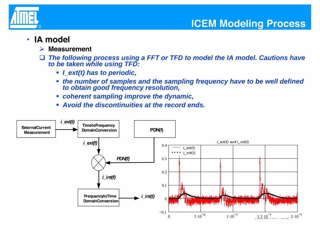
• IA modelMeasurementThe following process using a FFT or TFD to model the IA model. Cautions have to be taken while using TFD:
I_ext(t) has to periodic,the number of samples and the sampling frequency have to be well definedto obtain good frequency resolution, coherent sampling improve the dynamic,Avoid the discontinuities at the record ends.
ExternalCurrentMeasurement
TimetoFrequencyDomainConversion
FrequencytoTimeDomainConversion
PDN(f)
i_int(t)
i_ext(t)
i_ext(f)
i_int(f)
PDN(f)
_ Jluc LEVANT / Atmel
® ICEM Modeling Process
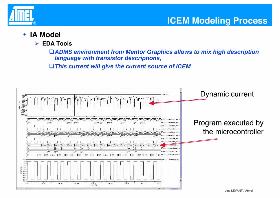
IA ModelEDA Tools
ADMS environment from Mentor Graphics allows to mix high description language with transistor descriptions,This current will give the current source of ICEM
Dynamic current
Program executed bythe microcontroller
_ Jluc LEVANT / Atmel
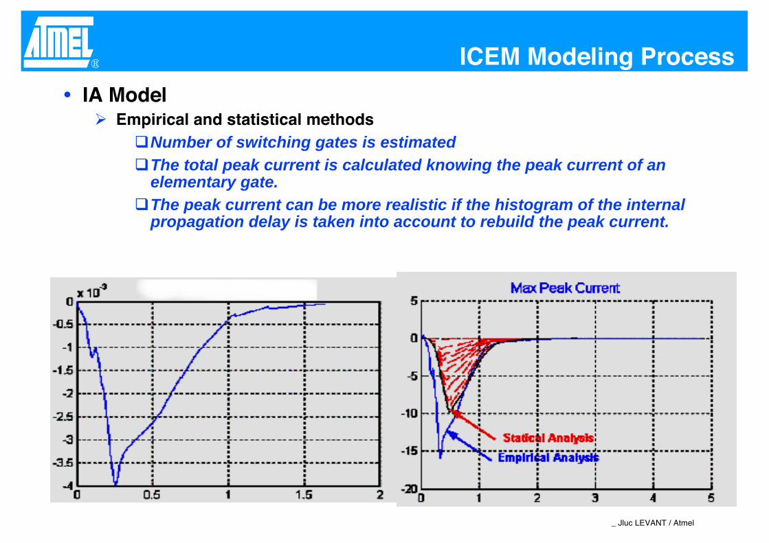
® ICEM Modeling Process
IA ModelEmpirical and statistical methods
Number of switching gates is estimatedThe total peak current is calculated knowing the peak current of anelementary gate.The peak current can be more realistic if the histogram of the internalpropagation delay is taken into account to rebuild the peak current.
_ Jluc LEVANT / Atmel
® Conclusions
ICEM is an IEC standard proposal IEC62014-3
ICEM models is built around two sub-model : PDN and IA,
ICEM model is opened model allowing to be described with lumped,distributed, S, … parameters,
ICEM is used to model the analog and digital activities,
ICEM will model Ios in the futur and can used others standard models such as IBIS, …
ICEM has been valided in differents applications and up to 2.5GHz