Embed Size (px)
Citation preview
DraculaDracula
CIC
1
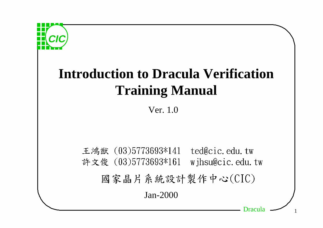
Introduction to Dracula VerificationTraining Manual
fÅ©�*�Ò7ÐYÄÿ)DJD*
Jan-2000
�í¦ )14*68847:4+252 ufeAdjd/fev/ux
Ñ�á )14*68847:4+272 xkitvAdjd/fev/ux
Ver. 1.0
DraculaDracula
CIC
2
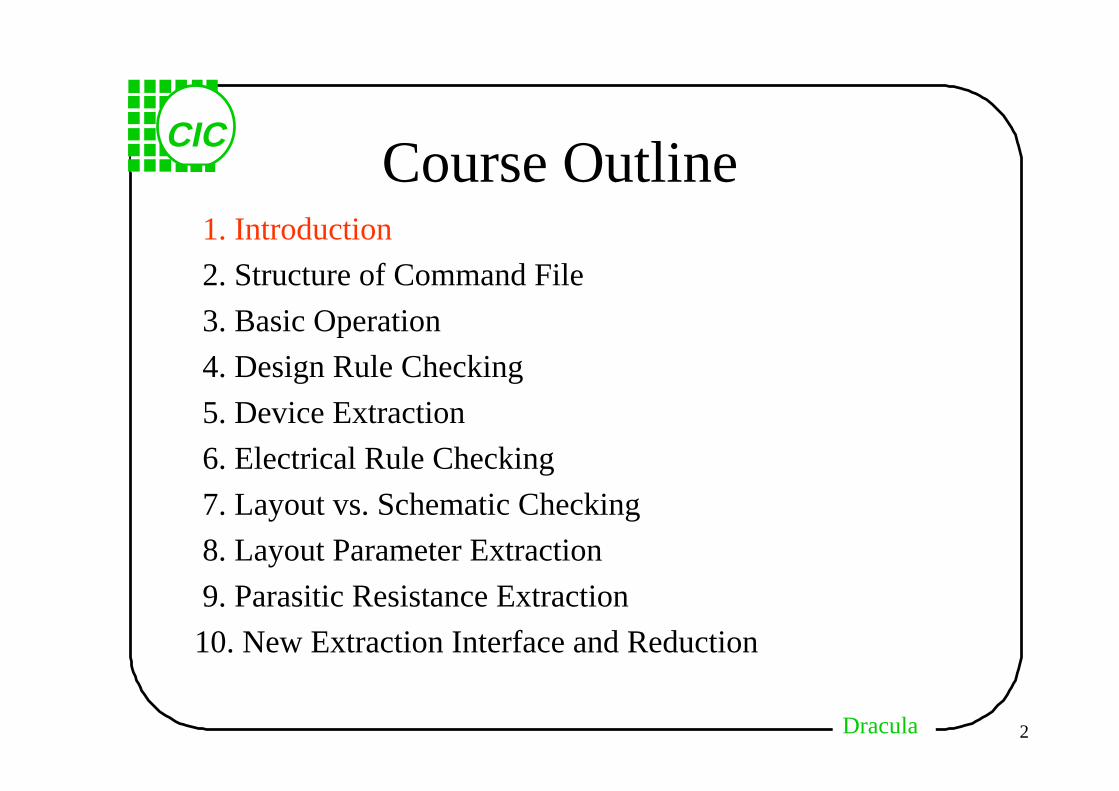
Course Outline 1. Introduction
2. Structure of Command File
3. Basic Operation
4. Design Rule Checking
5. Device Extraction
6. Electrical Rule Checking
7. Layout vs. Schematic Checking
8. Layout Parameter Extraction
9. Parasitic Resistance Extraction
10. New Extraction Interface and Reduction

DraculaDracula
CIC
3
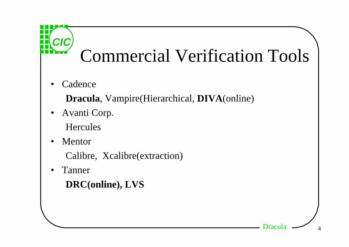
Commercial Verification Tools• Cadence
Dracula, Vampire(Hierarchical, DIVA (online)
• Avanti Corp.
Hercules
• Mentor
Calibre, Xcalibre(extraction)
• Tanner
DRC(online), LVS
DraculaDracula
CIC
4
Commercial Verification Tools• Cadence
Dracula, Vampire(Hierarchical, DIVA (online)
• Avanti Corp.
Hercules
• Mentor
Calibre, Xcalibre(extraction)
• Tanner
DRC(online), LVS
DraculaDracula
CIC
5
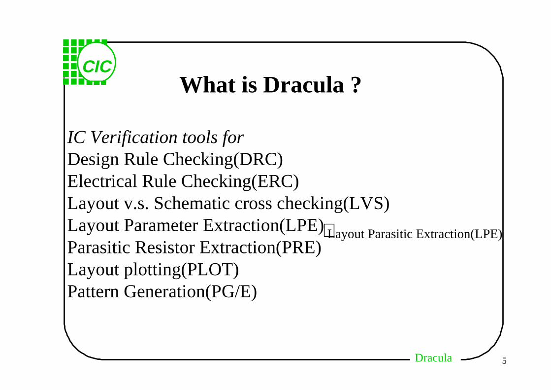
What is Dracula ?
IC Verification tools for Design Rule Checking(DRC)Electrical Rule Checking(ERC)Layout v.s. Schematic cross checking(LVS)Layout Parameter Extraction(LPE)Parasitic Resistor Extraction(PRE)Layout plotting(PLOT)Pattern Generation(PG/E)
⟩Layout Parasitic Extraction(LPE)
DraculaDracula
CIC
6
What is Dracula ?(cont’d)
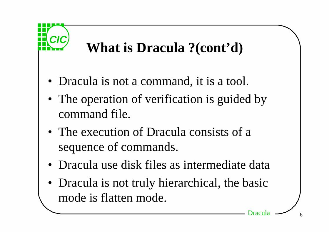
• Dracula is not a command, it is a tool.
• The operation of verification is guided bycommand file.
• The execution of Dracula consists of asequence of commands.
• Dracula use disk files as intermediate data
• Dracula is not truly hierarchical, the basicmode is flatten mode.
DraculaDracula
CIC
7
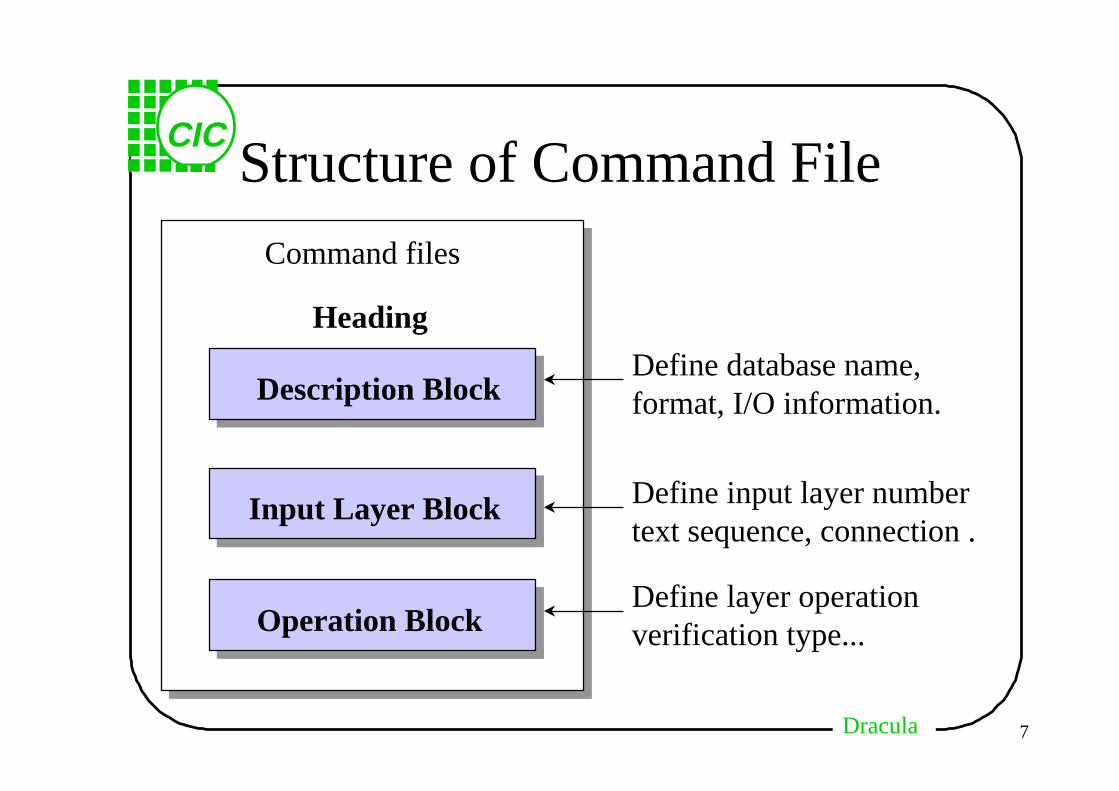
Structure of Command File
Description Block
Input Layer Block
Operation Block
Command files
Define database name,format, I/O information.
Define input layer numbertext sequence, connection .
Define layer operationverification type...
Heading
DraculaDracula
CIC
8
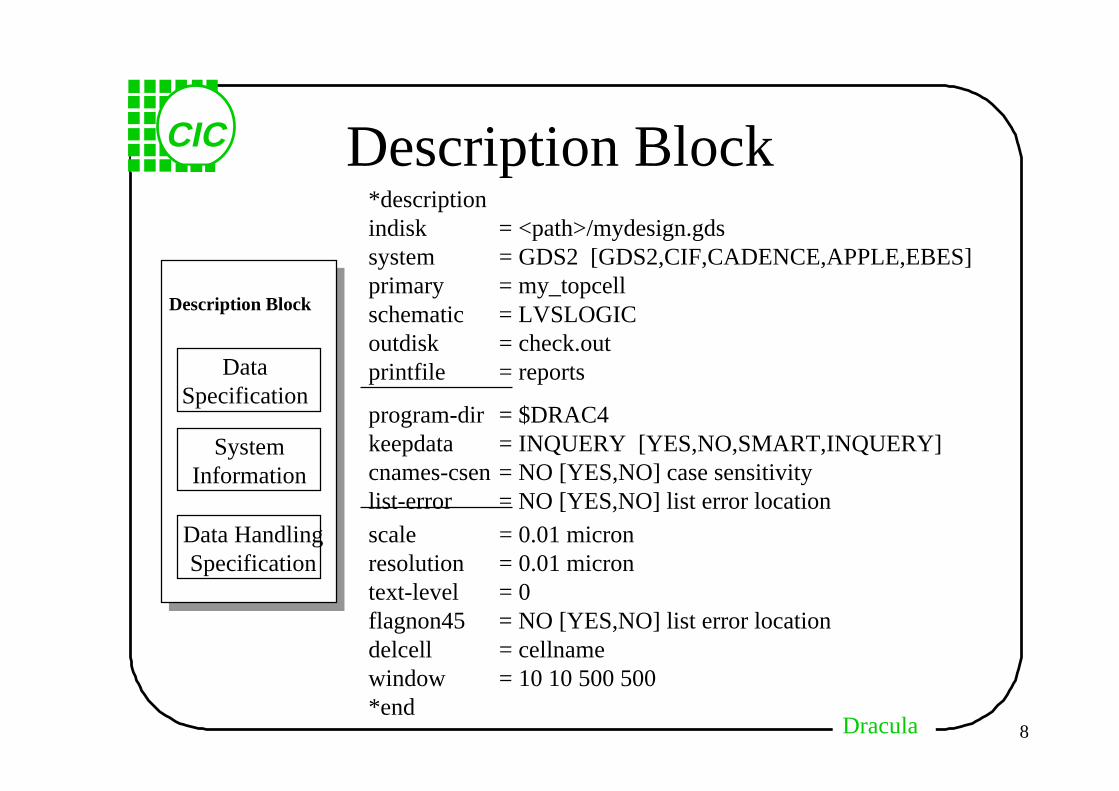
Description Block
Description Block
DataSpecification
SystemInformation
Data HandlingSpecification
*descriptionindisk = <path>/mydesign.gdssystem = GDS2 [GDS2,CIF,CADENCE,APPLE,EBES]primary = my_topcellschematic = LVSLOGICoutdisk = check.outprintfile = reports
program-dir = $DRAC4keepdata = INQUERY [YES,NO,SMART,INQUERY]cnames-csen = NO [YES,NO] case sensitivitylist-error = NO [YES,NO] list error location
scale = 0.01 micronresolution = 0.01 microntext-level = 0flagnon45 = NO [YES,NO] list error locationdelcell = cellnamewindow = 10 10 500 500*end
DraculaDracula
CIC
9
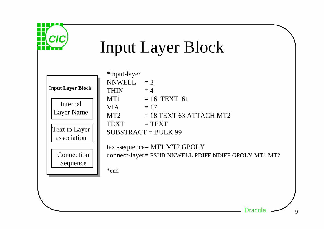
Input Layer Block
Input Layer Block
InternalLayer Name
Text to Layerassociation
ConnectionSequence
*input-layerNNWELL = 2THIN = 4MT1 = 16 TEXT 61VIA = 17MT2 = 18 TEXT 63 ATTACH MT2TEXT = TEXTSUBSTRACT = BULK 99
text-sequence= MT1 MT2 GPOLYconnect-layer= PSUB NNWELL PDIFF NDIFF GPOLY MT1 MT2
*end
DraculaDracula
CIC
10
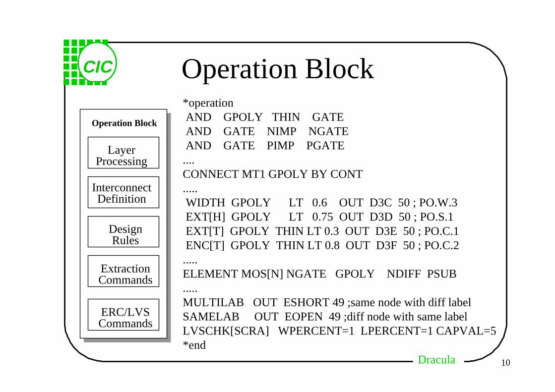
Operation Block
Operation Block
LayerProcessing
InterconnectDefinition
DesignRules
ExtractionCommands
ERC/LVSCommands
*operation AND GPOLY THIN GATE AND GATE NIMP NGATE AND GATE PIMP PGATE....CONNECT MT1 GPOLY BY CONT..... WIDTH GPOLY LT 0.6 OUT D3C 50 ; PO.W.3 EXT[H] GPOLY LT 0.75 OUT D3D 50 ; PO.S.1 EXT[T] GPOLY THIN LT 0.3 OUT D3E 50 ; PO.C.1 ENC[T] GPOLY THIN LT 0.8 OUT D3F 50 ; PO.C.2.....ELEMENT MOS[N] NGATE GPOLY NDIFF PSUB.....MULTILAB OUT ESHORT 49 ;same node with diff labelSAMELAB OUT EOPEN 49 ;diff node with same labelLVSCHK[SCRA] WPERCENT=1 LPERCENT=1 CAPVAL=5*end
DraculaDracula
CIC
11
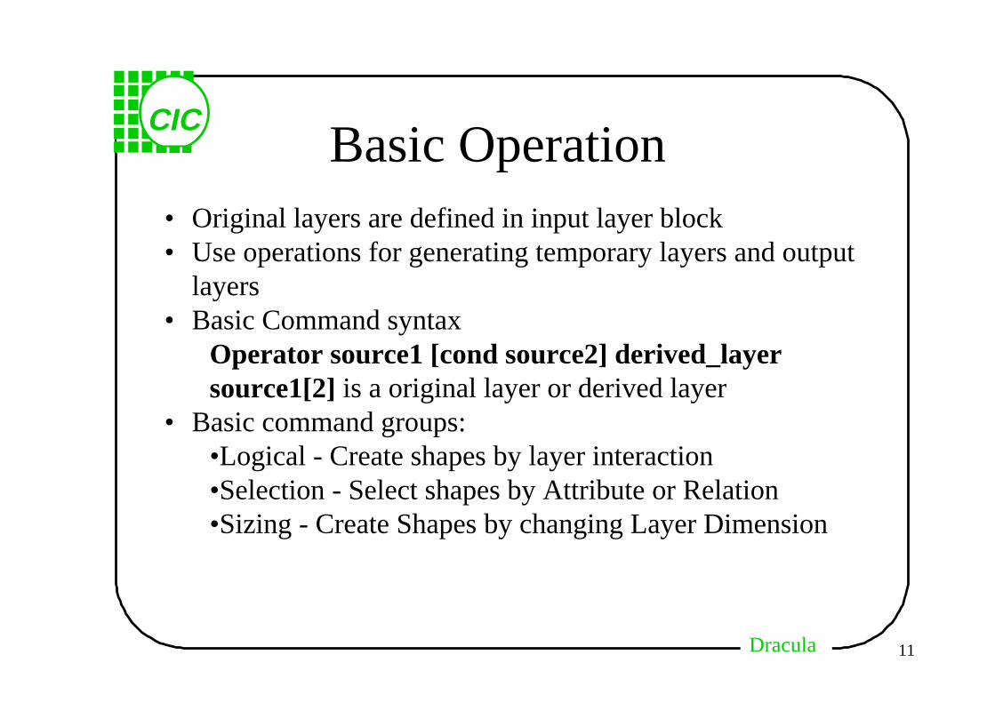
Basic Operation• Original layers are defined in input layer block• Use operations for generating temporary layers and output
layers• Basic Command syntax
Operator source1 [cond source2] derived_layersource1[2] is a original layer or derived layer
• Basic command groups:•Logical - Create shapes by layer interaction•Selection - Select shapes by Attribute or Relation•Sizing - Create Shapes by changing Layer Dimension
DraculaDracula
CIC
12
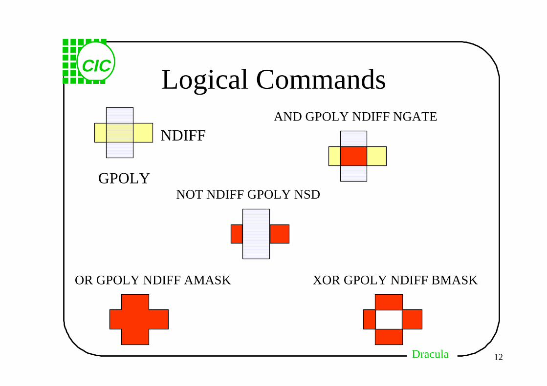
Logical Commands
GPOLY
NDIFFAND GPOLY NDIFF NGATE
OR GPOLY NDIFF AMASK XOR GPOLY NDIFF BMASK
NOT NDIFF GPOLY NSD
DraculaDracula
CIC
13
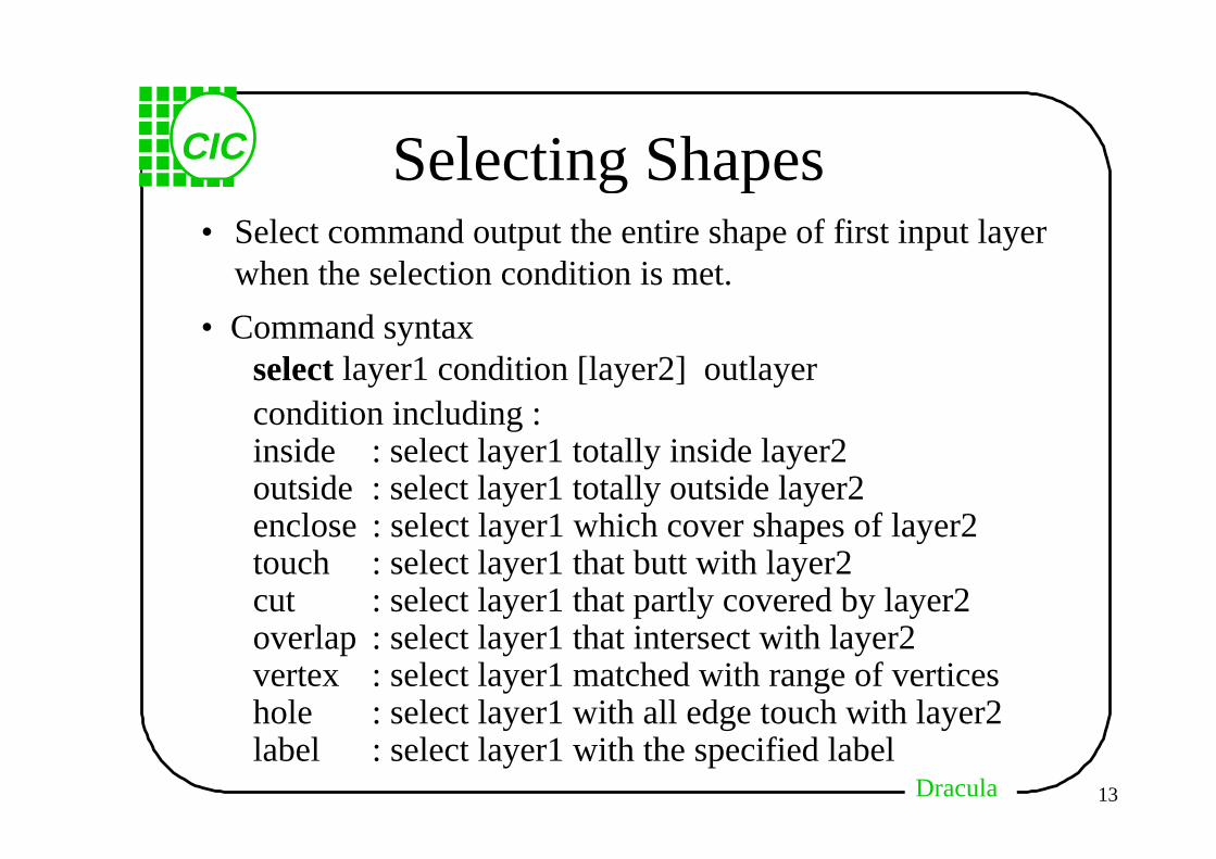
Selecting Shapes• Select command output the entire shape of first input layer
when the selection condition is met.
• Command syntaxselect layer1 condition [layer2] outlayercondition including :inside : select layer1 totally inside layer2outside : select layer1 totally outside layer2enclose : select layer1 which cover shapes of layer2touch : select layer1 that butt with layer2cut : select layer1 that partly covered by layer2overlap : select layer1 that intersect with layer2vertex : select layer1 matched with range of verticeshole : select layer1 with all edge touch with layer2label : select layer1 with the specified label
DraculaDracula
CIC
14
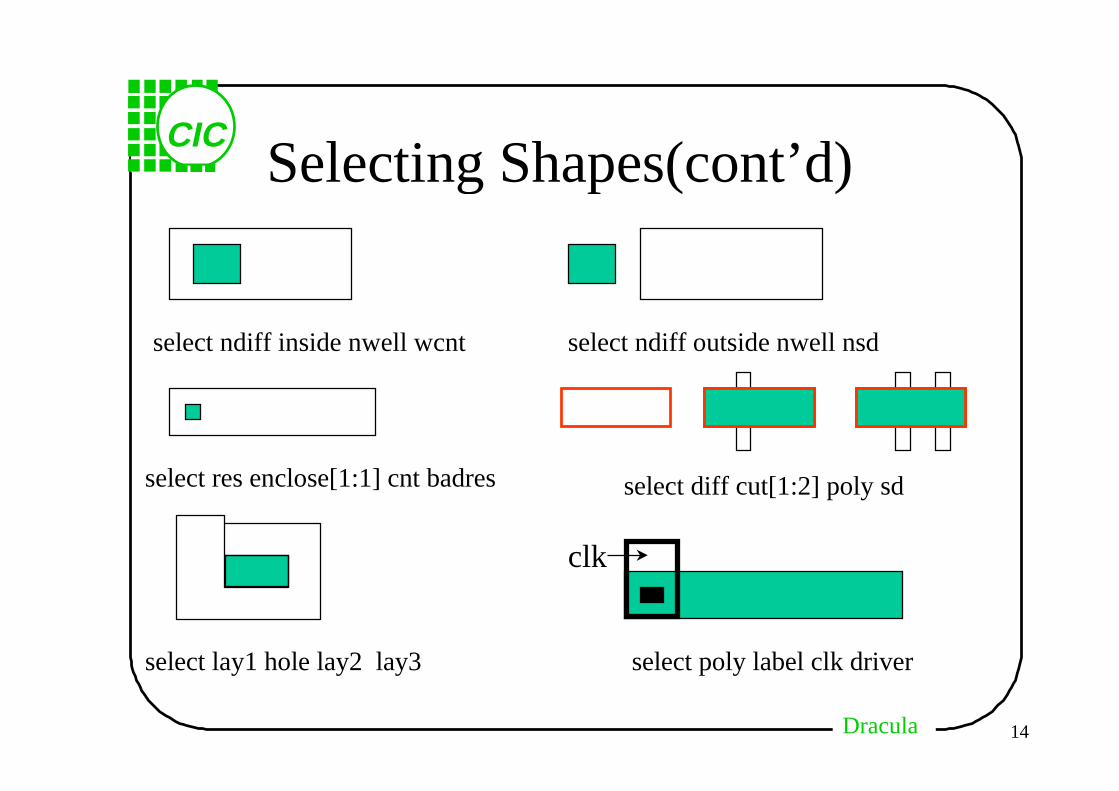
Selecting Shapes(cont’d)
select ndiff inside nwell wcnt select ndiff outside nwell nsd
select res enclose[1:1] cnt badres
select lay1 hole lay2 lay3
select diff cut[1:2] poly sd
clk
select poly label clk driver
DraculaDracula
CIC
15
Sizing ShapesCommand syntax:
SIZE layer by value outlayervalue > 0 expansionvalue < 0 shrink
SIZE operation is four direction
Additional usage of SIZE operation :
1.5u
merge object
SIZE lay1 by 1.5u lay2SIZE lay2 by -1.5u lay3
DraculaDracula
CIC
16
Sizing Shapes (cont’d)Usage of size operation : split object
SIZE layer1 by -1 layer2SIZE layer2 by 1 layer3
GROWSHRINK
oversize two perpendicular edgesUndersize two perpendicular edges
grow lay1 2 1 lay2 shrink lay1 -1.5 1 lay2
1u2u 1u1.5u
DraculaDracula
CIC
17
Design Rule Checking
• ��`´Ò7Ð*Ìõ���û
• nxÒ7Ìõ<�ÑbÇ Width, Spacing îÃÌbËÇspacing ìenclosure 2�æ
• Design rule �ÌÊyn$ process variation,equipment limitation, circuit reliability 2Ç,½
• ÞT/�Ò7�ú�ëDesign rule ÙÑô´�oûíWÒ7����rule violation ð�X�pÓí
DraculaDracula
CIC
18
Typical Design Rules
abc
d
e
f
a : WIDTH
b,c : EXT
d,f : ENC
e : INT
minimum width of geometry
minimum spacing of objects - outer edge to outer edge
minimum spacing of objects - inner edge to outer edge
minimum spacing of objects - inner edge to inner edge
DraculaDracula
CIC
19
DRC Commands
CMD[mod] lay1 [lay2] cond_chk OUTPUT cellname laynum
Basic type 1 : ouptut check mark to select layer
CMD : width , area, ext, enc, int , overlap, plength
cond_chk : lt , le, range, gt, ge
cellname : output to cell namelaynum : output with layer number
CMD[mod] lay1 [lay2] sel_cond_chk cellname
Basic type 2 : output selected object to layer
sel_cond_chk : sellt, selle, selra, selgt, selge
mod : c, c’, n, n’ , p, p’ , r , r’ , t, o, e, s command modifiers
DraculaDracula
CIC
20
DRC Commands(cont’d)ext[T] GPOLY THIN LT 0.3 OUT D3E 50 ; PO.C.1
0.4u
ext[T] THIN GPOLY SELLT 0.3 TMP1
One check per command lineCan be conjuncted with ‘&’ mark
ENC[T] GATE&G1 GPOLY LT 0.005 &ENC[PT] &G1 PIMP LT 0.75 OUT D4E 50 ; PP.C.3
DraculaDracula
CIC
21
Command Modifiers
c : parallelc’ : not parallel
ext[c] ext[c’]
n : same netn’ : different net
p : projection p’ : not projection
r : region output r’ : outer region
ext[n] ext[n’]
ext[p] ext[p’]
ext[r] ext[r’]
t : touch e : not enclosedo : overlap s : square corner
DraculaDracula
CIC
22
Data Integrity Check
This kind of check is specified in Description block
FLAG-OFFGRID = YES
FLAG-SELFINTERS = YES
FLAG-ACUTEANGLE = YES
DraculaDracula
CIC
23
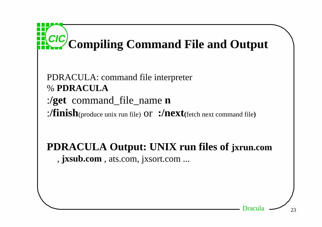
Compiling Command File and Output
PDRACULA: command file interpreter% PDRACULA:/get command_file_name n:/finish(produce unix run file) or :/next(fetch next command file)
PDRACULA Output: UNIX run files of jxrun.com, jxsub.com , ats.com, jxsort.com ...
DraculaDracula
CIC
24
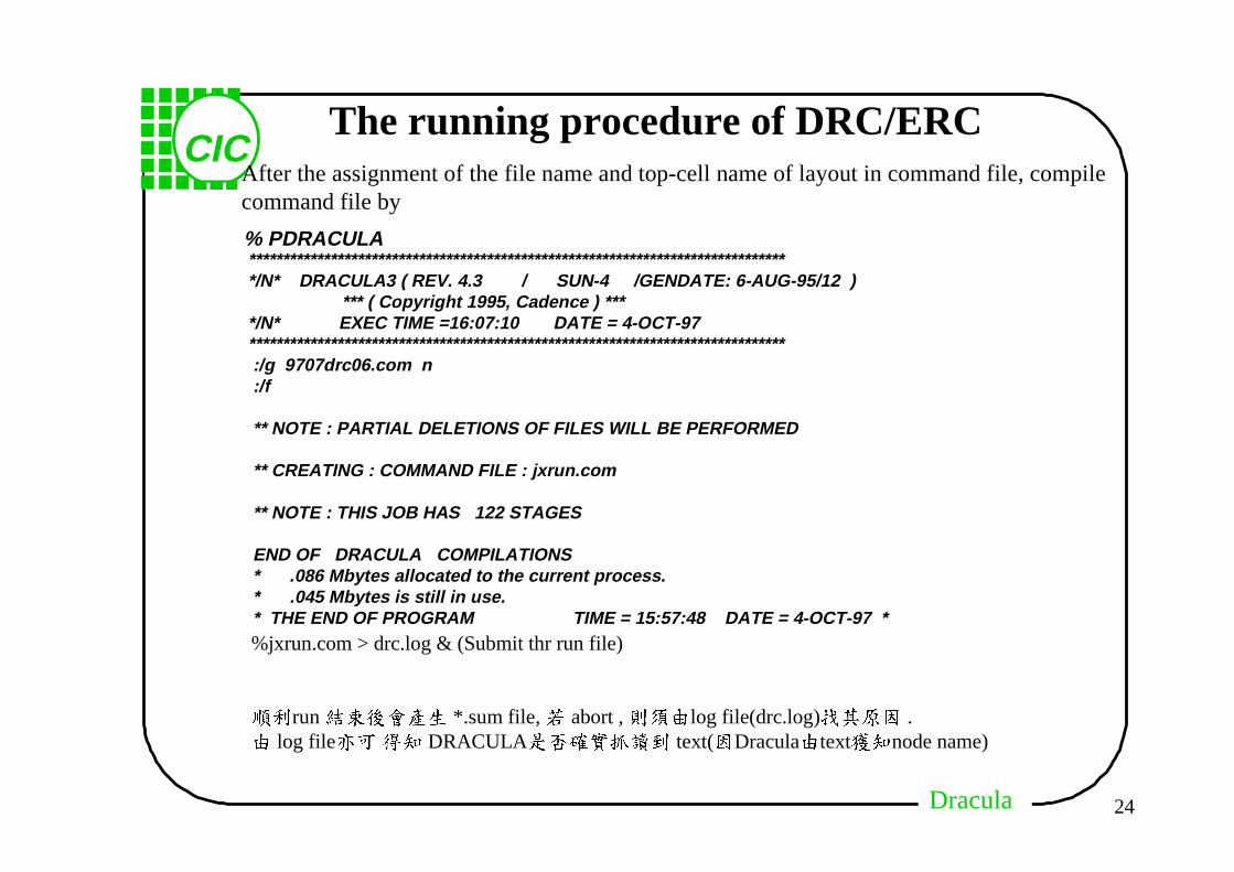
% PDRACULA********************************************************************************/N* DRACULA3 ( REV. 4.3 / SUN-4 /GENDATE: 6-AUG-95/12 ) *** ( Copyright 1995, Cadence ) ****/N* EXEC TIME =16:07:10 DATE = 4-OCT-97******************************************************************************* :/g 9707drc06.com n :/f
** NOTE : PARTIAL DELETIONS OF FILES WILL BE PERFORMED
** CREATING : COMMAND FILE : jxrun.com
** NOTE : THIS JOB HAS 122 STAGES
END OF DRACULA COMPILATIONS * .086 Mbytes allocated to the current process. * .045 Mbytes is still in use. * THE END OF PROGRAM TIME = 15:57:48 DATE = 4-OCT-97 *%jxrun.com > drc.log & (Submit thr run file)
àjrun ?ëLeY� *.sum file, abort , õá�log file(drc.log)Ûx�Ù .� log file¤H ª� DRACULAyxëëã�� text(ÙDracula�text>�node name)
The running procedure of DRC/ERCAfter the assignment of the file name and top-cell name of layout in command file, compile command file by
DraculaDracula
CIC
25
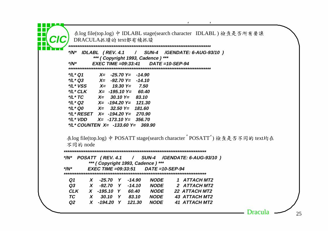
********************************************************************************/N* IDLABL ( REV. 4.1 / SUN-4 /GENDATE: 6-AUG-93/10 ) *** ( Copyright 1993, Cadence ) ****/N* EXEC TIME =09:33:41 DATE =10-SEP-94********************************************************************************/L* Q1 X= -25.70 Y= -14.90*/L* Q3 X= -92.70 Y= -14.10*/L* VSS X= 19.30 Y= 7.50*/L* CLK X= -195.10 Y= 60.40*/L* TC X= 30.10 Y= 83.10*/L* Q2 X= -194.20 Y= 121.30*/L* Q0 X= 32.50 Y= 181.60*/L* RESET X= -194.20 Y= 270.90*/L* VDD X= -173.10 Y= 356.70*/L* COUNTEN X= -133.60 Y= 369.90
Þlog file(top.log) Ä IDLABL stage(search character IDLABL ) ��yx� 5ZDRACULAã�� textö Æã�
‘‘
Þlog file(top.log) Ä POSATT stage(search character POSATT ) ��yxÃÌ� text�ÞÃÌ� node
‘‘
********************************************************************************/N* POSATT ( REV. 4.1 / SUN-4 /GENDATE: 6-AUG-93/10 ) *** ( Copyright 1993, Cadence ) ****/N* EXEC TIME =09:33:51 DATE =10-SEP-94******************************************************************************* Q1 X -25.70 Y -14.90 NODE 1 ATTACH MT2 Q3 X -92.70 Y -14.10 NODE 2 ATTACH MT2 CLK X -195.10 Y 60.40 NODE 22 ATTACH MT2 TC X 30.10 Y 83.10 NODE 43 ATTACH MT2 Q2 X -194.20 Y 121.30 NODE 41 ATTACH MT2
DraculaDracula
CIC
26
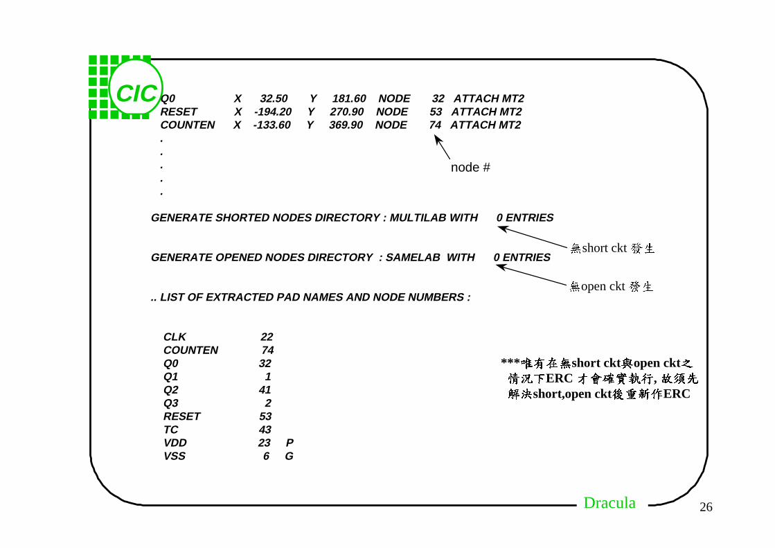
Q0 X 32.50 Y 181.60 NODE 32 ATTACH MT2 RESET X -194.20 Y 270.90 NODE 53 ATTACH MT2 COUNTEN X -133.60 Y 369.90 NODE 74 ATTACH MT2 . . . . .
GENERATE SHORTED NODES DIRECTORY : MULTILAB WITH 0 ENTRIES
GENERATE OPENED NODES DIRECTORY : SAMELAB WITH 0 ENTRIES
.. LIST OF EXTRACTED PAD NAMES AND NODE NUMBERS :
CLK 22 COUNTEN 74 Q0 32 Q1 1 Q2 41 Q3 2 RESET 53 TC 43 VDD 23 P VSS 6 G
node #
ûshort ckt ��
ûopen ckt ��
*** [ Þûshort cktopen cktÇ º`�ERC Àeëëq@, qẠ5�short,open cktLP\YERC
DraculaDracula
CIC
27
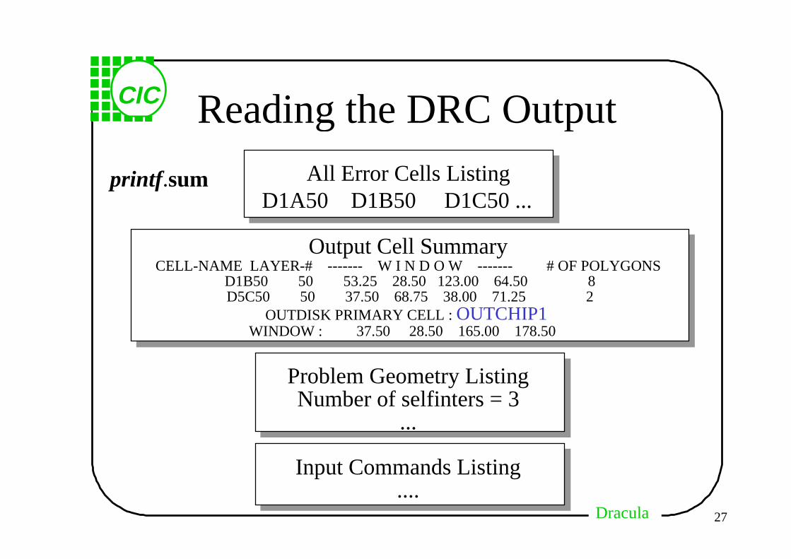
Reading the DRC Output
All Error Cells ListingD1A50 D1B50 D1C50 ...
Output Cell SummaryCELL-NAME LAYER-# ------- W I N D O W ------- # OF POLYGONS
D1B50 50 53.25 28.50 123.00 64.50 8 D5C50 50 37.50 68.75 38.00 71.25 2
OUTDISK PRIMARY CELL : OUTCHIP1 WINDOW : 37.50 28.50 165.00 178.50
Problem Geometry ListingNumber of selfinters = 3
...
Input Commands Listing....
printf .sum
DraculaDracula
CIC
28
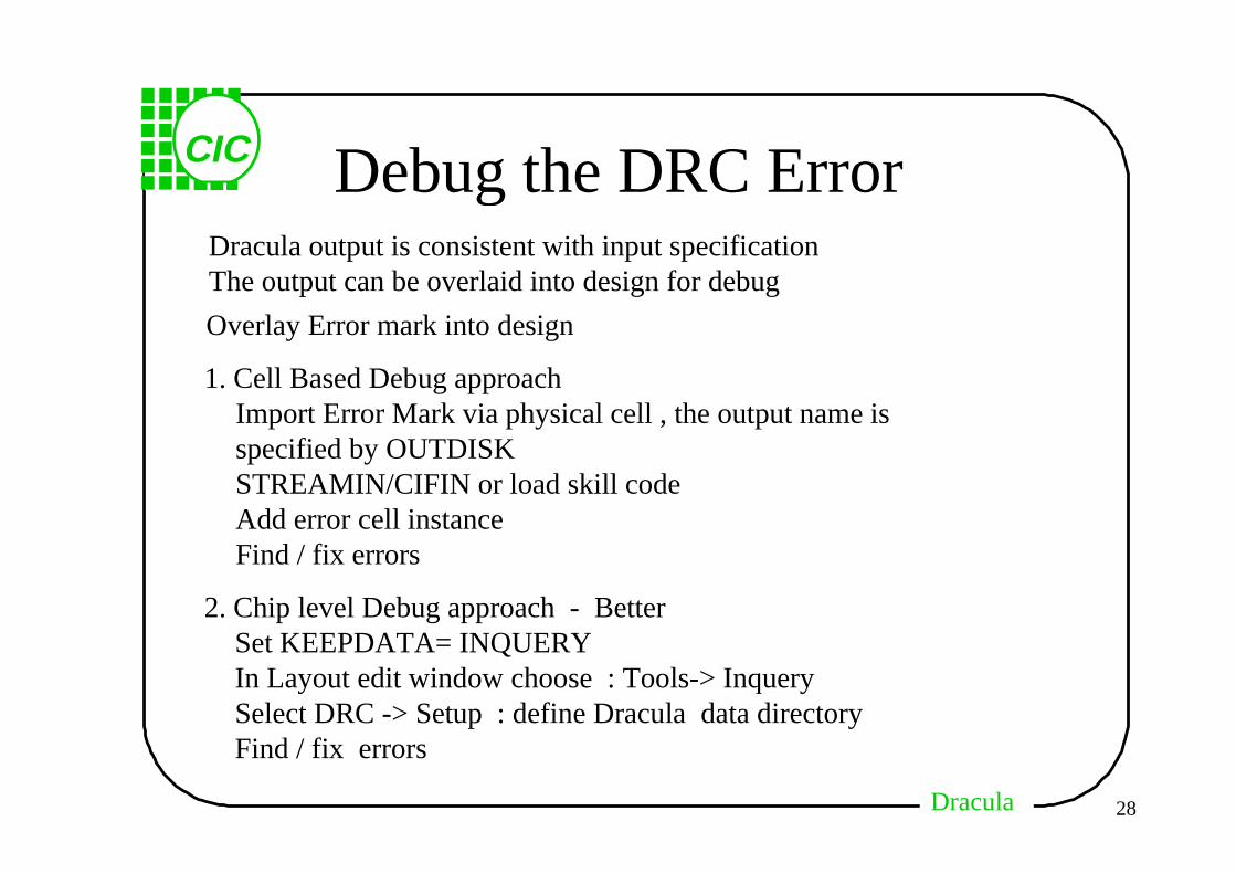
Debug the DRC ErrorDracula output is consistent with input specificationThe output can be overlaid into design for debug
Overlay Error mark into design
1. Cell Based Debug approach
2. Chip level Debug approach - Better
Import Error Mark via physical cell , the output name isspecified by OUTDISKSTREAMIN/CIFIN or load skill codeAdd error cell instanceFind / fix errors
Set KEEPDATA= INQUERYIn Layout edit window choose : Tools-> InquerySelect DRC -> Setup : define Dracula data directoryFind / fix errors
DraculaDracula
CIC
29
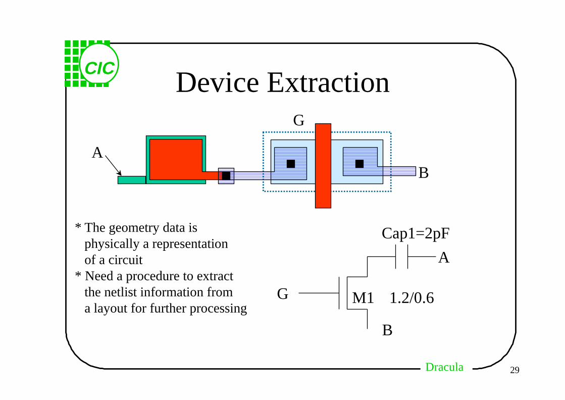
Device Extraction
AB
G
G
A
B
Cap1=2pF
M1 1.2/0.6
* The geometry data is physically a representationof a circuit
* Need a procedure to extractthe netlist information froma layout for further processing
DraculaDracula
CIC
30
Device Extraction(cont’d)• GDS2 Data is only geometrical information, such as
rectangle, path, polygon ...
• Using device extraction for creating electrical information
• Define the connection properties of layers
• Define the device structure of a layout database
• Create electrical connectivity with text label
• Only for normal devices such as MOS, BJT, DIODE,RESISTOR, CAPACITOR
• Device extraction for further usage : ERC / LVS
DraculaDracula
CIC
31
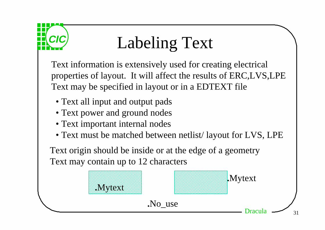
Labeling TextText information is extensively used for creating electrical properties of layout. It will affect the results of ERC,LVS,LPEText may be specified in layout or in a EDTEXT file
• Text all input and output pads• Text power and ground nodes• Text important internal nodes• Text must be matched between netlist/ layout for LVS, LPE
Text origin should be inside or at the edge of a geometryText may contain up to 12 characters
.Mytext.Mytext
.No_use
DraculaDracula
CIC
32
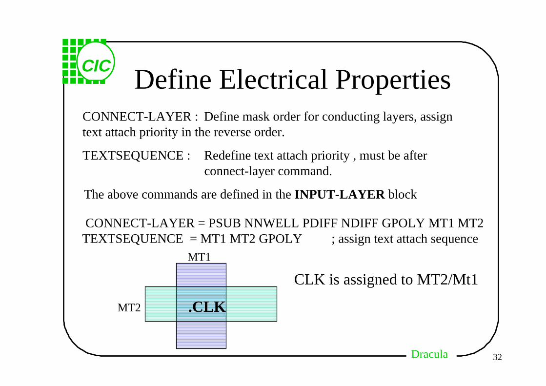
Define Electrical Properties
CONNECT-LAYER = PSUB NNWELL PDIFF NDIFF GPOLY MT1 MT2TEXTSEQUENCE = MT1 MT2 GPOLY ; assign text attach sequence
CONNECT-LAYER : Define mask order for conducting layers, assign text attach priority in the reverse order.
TEXTSEQUENCE : Redefine text attach priority , must be after connect-layer command.
The above commands are defined in the INPUT-LAYER block
.CLK
MT1
MT2
CLK is assigned to MT2/Mt1
DraculaDracula
CIC
33
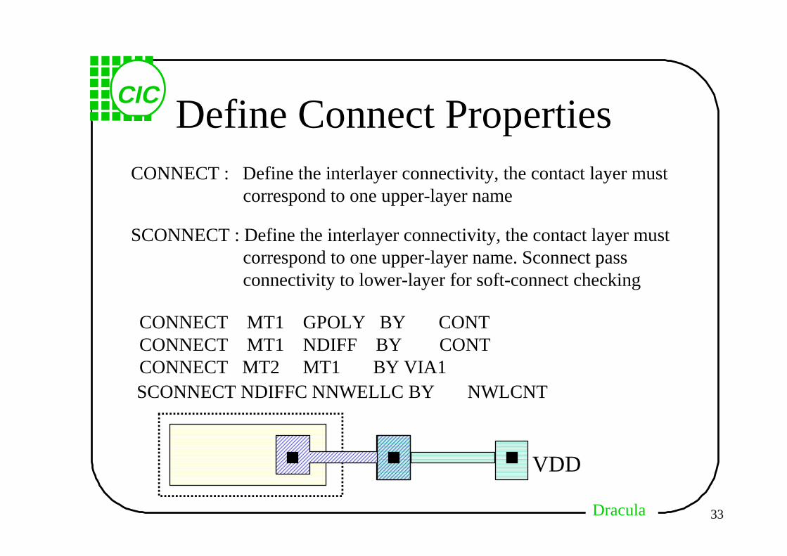
Define Connect PropertiesCONNECT : Define the interlayer connectivity, the contact layer must
correspond to one upper-layer name
SCONNECT : Define the interlayer connectivity, the contact layer mustcorrespond to one upper-layer name. Sconnect pass connectivity to lower-layer for soft-connect checking
CONNECT MT1 GPOLY BY CONTCONNECT MT1 NDIFF BY CONTCONNECT MT2 MT1 BY VIA1SCONNECT NDIFFC NNWELLC BY NWLCNT
VDD
DraculaDracula
CIC
34
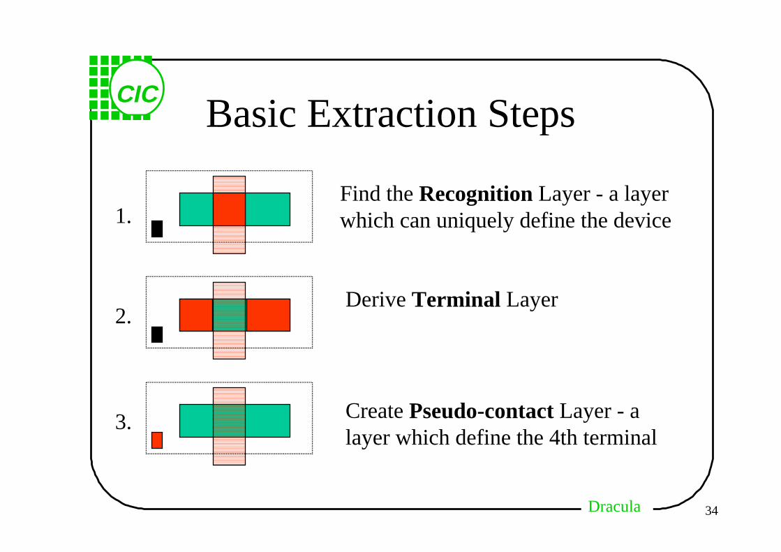
Basic Extraction Steps
Find the Recognition Layer - a layerwhich can uniquely define the device1.
2.Derive Terminal Layer
3. Create Pseudo-contact Layer - alayer which define the 4th terminal
DraculaDracula
CIC
35
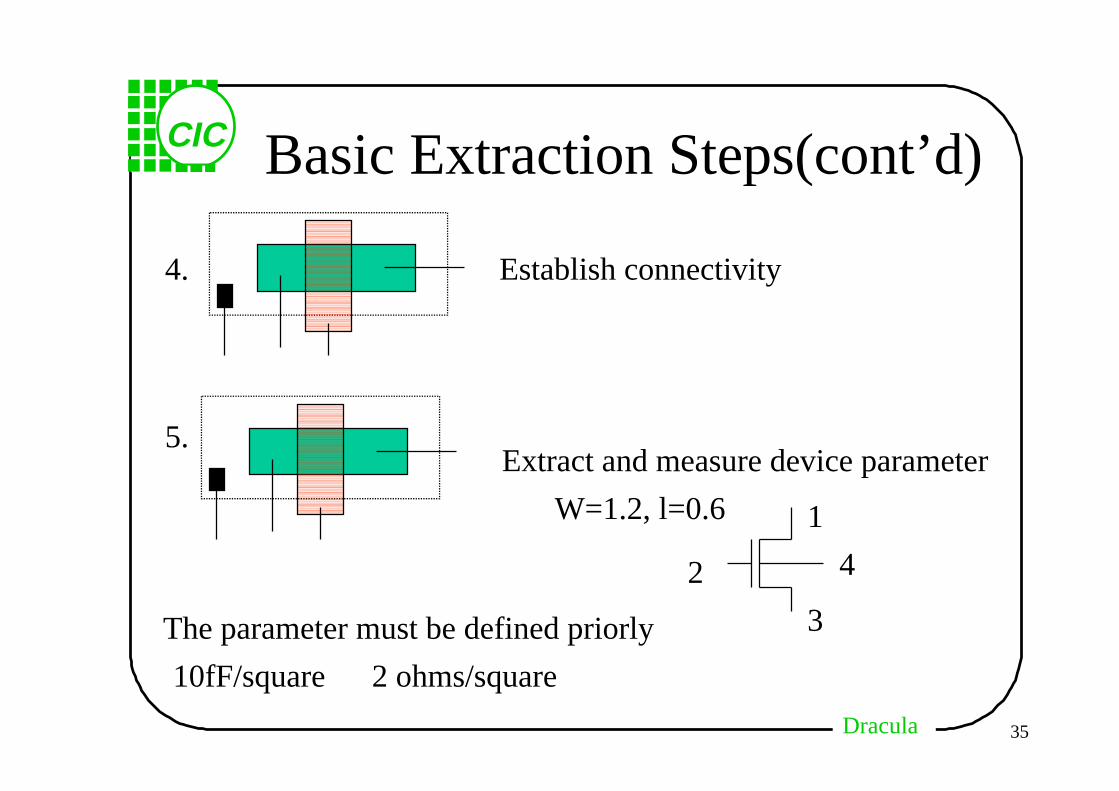
Basic Extraction Steps(cont’d)
4. Establish connectivity
5.Extract and measure device parameter
W=1.2, l=0.6
2
1
4
3The parameter must be defined priorly
10fF/square 2 ohms/square
DraculaDracula
CIC
36
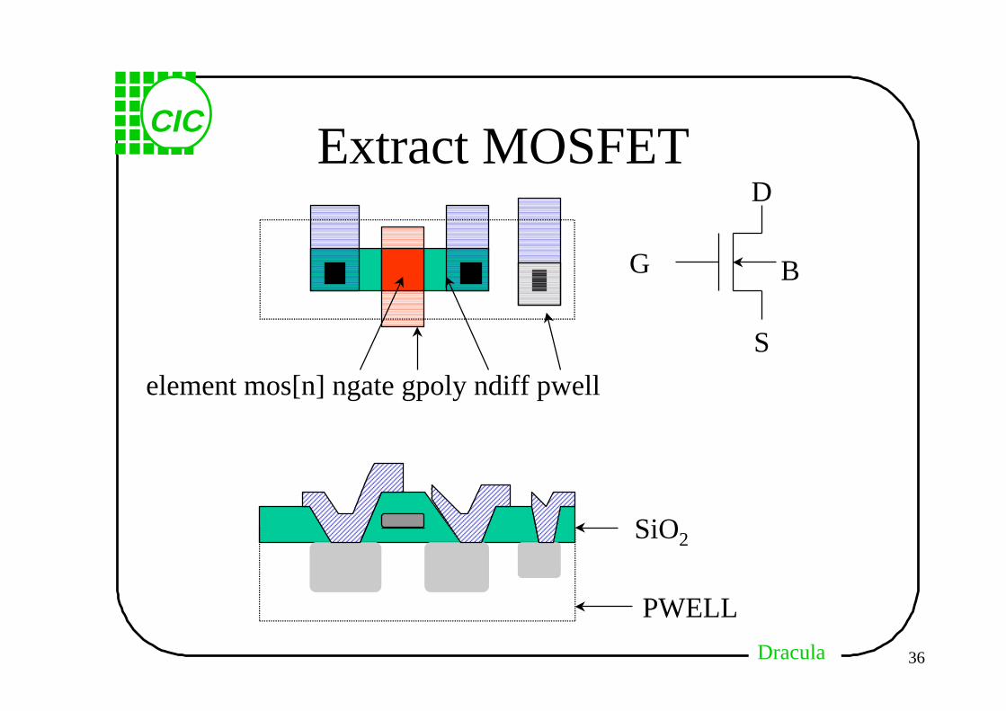
Extract MOSFET
element mos[n] ngate gpoly ndiff pwell
G
D
S
B
SiO2
PWELL
DraculaDracula
CIC
37
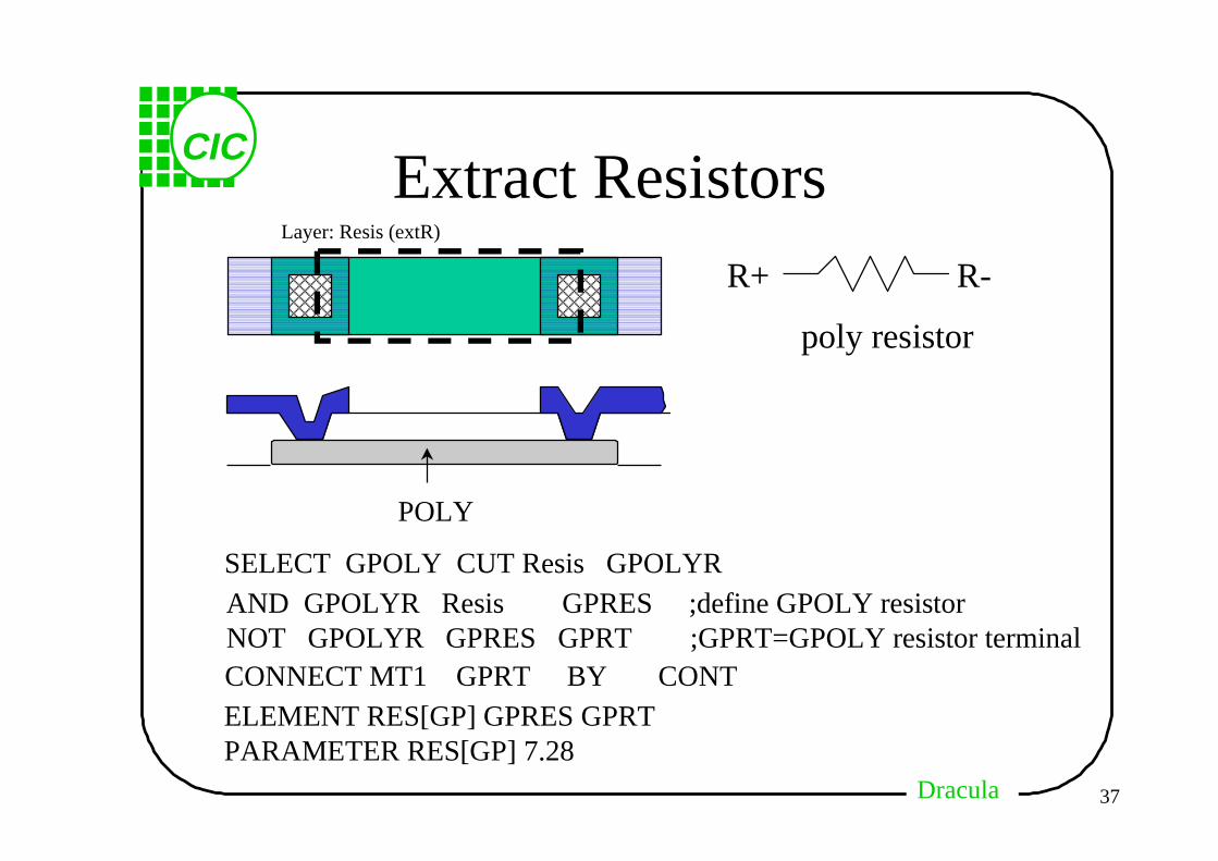
Extract Resistors
R+ R-
poly resistor
SELECT GPOLY CUT Resis GPOLYR AND GPOLYR Resis GPRES ;define GPOLY resistor NOT GPOLYR GPRES GPRT ;GPRT=GPOLY resistor terminalCONNECT MT1 GPRT BY CONT ELEMENT RES[GP] GPRES GPRT PARAMETER RES[GP] 7.28
POLY
Layer: Resis (extR)
DraculaDracula
CIC
38
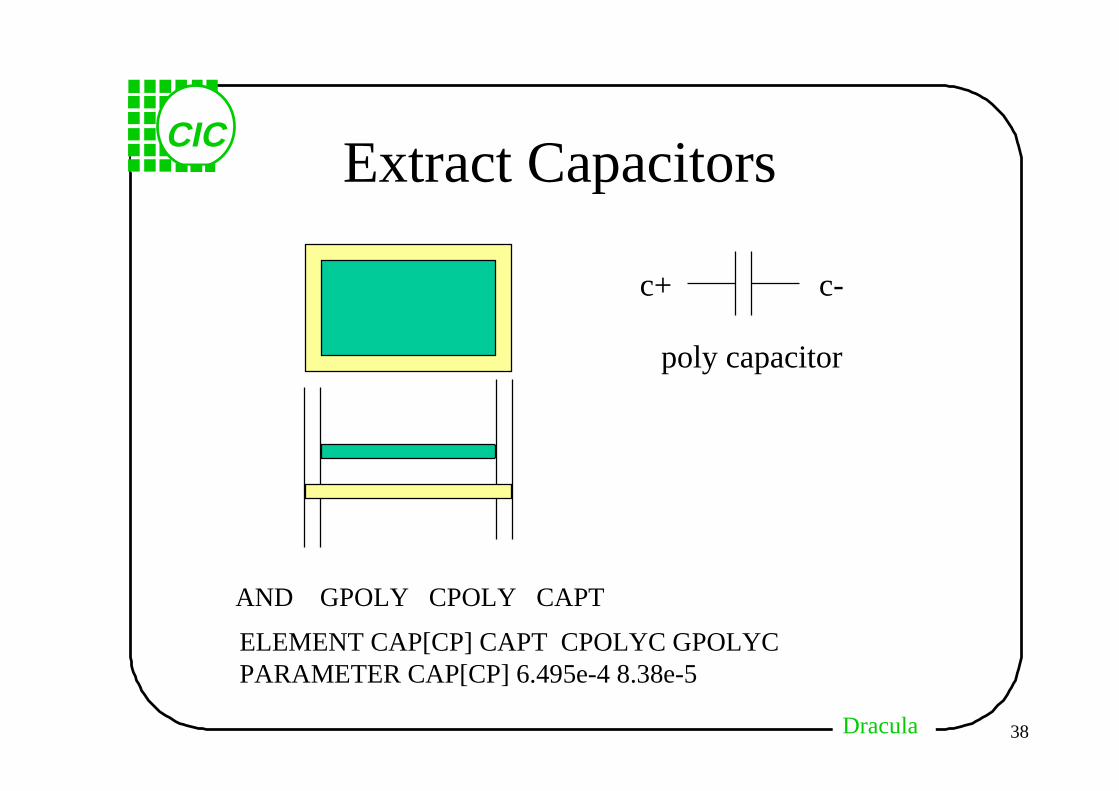
Extract Capacitors
poly capacitor
c+ c-
ELEMENT CAP[CP] CAPT CPOLYC GPOLYC PARAMETER CAP[CP] 6.495e-4 8.38e-5
AND GPOLY CPOLY CAPT
DraculaDracula
CIC
39
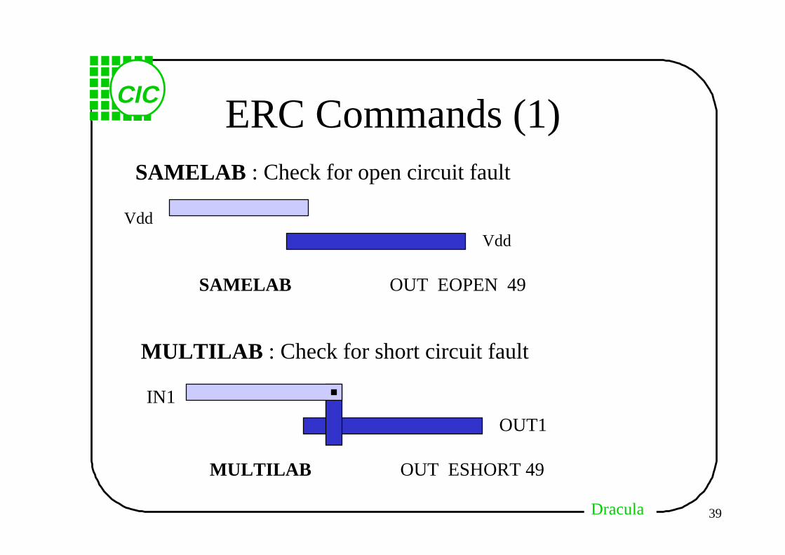
ERC Commands (1)SAMELAB : Check for open circuit fault
MULTILAB : Check for short circuit fault
VddVdd
SAMELAB OUT EOPEN 49
IN1
OUT1
MULTILAB OUT ESHORT 49
DraculaDracula
CIC
40
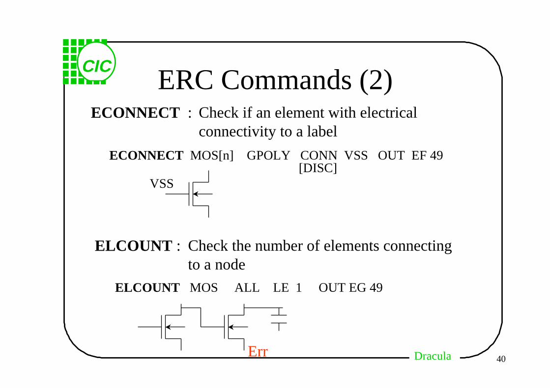
ERC Commands (2)
ELCOUNT MOS ALL LE 1 OUT EG 49
ECONNECT : Check if an element with electricalconnectivity to a label
ECONNECT MOS[n] GPOLY CONN VSS OUT EF 49
VSS[DISC]
ELCOUNT : Check the number of elements connectingto a node
Err
DraculaDracula
CIC
41
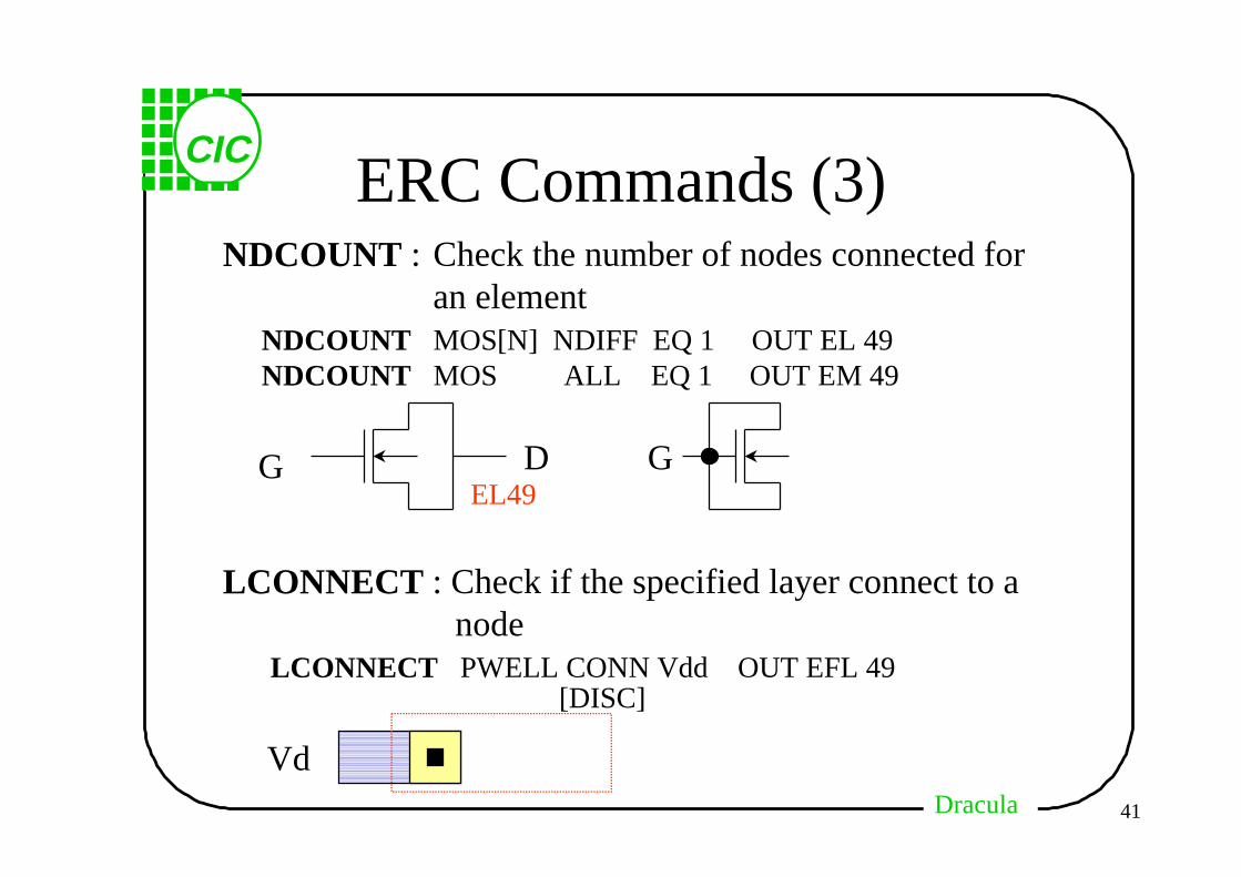
ERC Commands (3)
NDCOUNT MOS[N] NDIFF EQ 1 OUT EL 49NDCOUNT MOS ALL EQ 1 OUT EM 49
NDCOUNT : Check the number of nodes connected foran element
G D GEL49
LCONNECT : Check if the specified layer connect to anode
LCONNECT PWELL CONN Vdd OUT EFL 49[DISC]
Vd
DraculaDracula
CIC
42
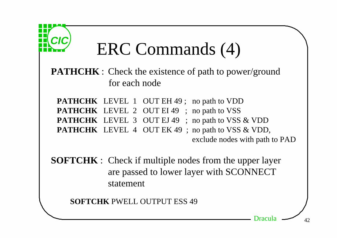
ERC Commands (4)PATHCHK : Check the existence of path to power/ground
for each node
PATHCHK LEVEL 1 OUT EH 49 ; no path to VDDPATHCHK LEVEL 2 OUT EI 49 ; no path to VSSPATHCHK LEVEL 3 OUT EJ 49 ; no path to VSS & VDDPATHCHK LEVEL 4 OUT EK 49 ; no path to VSS & VDD,
exclude nodes with path to PAD
SOFTCHK : Check if multiple nodes from the upper layerare passed to lower layer with SCONNECT statement
SOFTCHK PWELL OUTPUT ESS 49
DraculaDracula
CIC
43
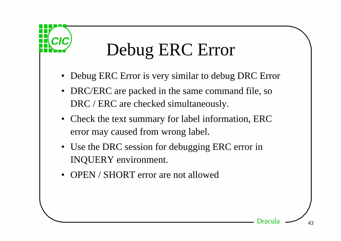
Debug ERC Error• Debug ERC Error is very similar to debug DRC Error
• DRC/ERC are packed in the same command file, soDRC / ERC are checked simultaneously.
• Check the text summary for label information, ERCerror may caused from wrong label.
• Use the DRC session for debugging ERC error in INQUERY environment.
• OPEN / SHORT error are not allowed
DraculaDracula
CIC
44
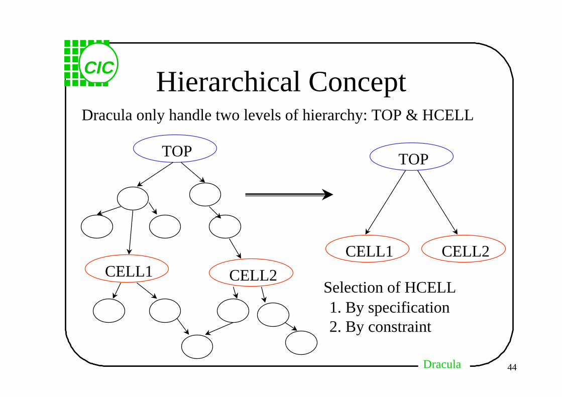
Hierarchical ConceptDracula only handle two levels of hierarchy: TOP & HCELL
TOP
CELL1 CELL2
TOP
CELL1 CELL2
Selection of HCELL1. By specification2. By constraint
DraculaDracula
CIC
45
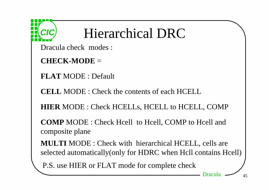
Hierarchical DRCDracula check modes :
FLAT MODE : Default
CELL MODE : Check the contents of each HCELL
COMP MODE : Check Hcell to Hcell, COMP to Hcell andcomposite plane
HIER MODE : Check HCELLs, HCELL to HCELL, COMP
MULTI MODE : Check with hierarchical HCELL, cells areselected automatically(only for HDRC when Hcll contains Hcell)
CHECK-MODE =
P.S. use HIER or FLAT mode for complete check
DraculaDracula
CIC
46
Hierarchical DRC/ERC
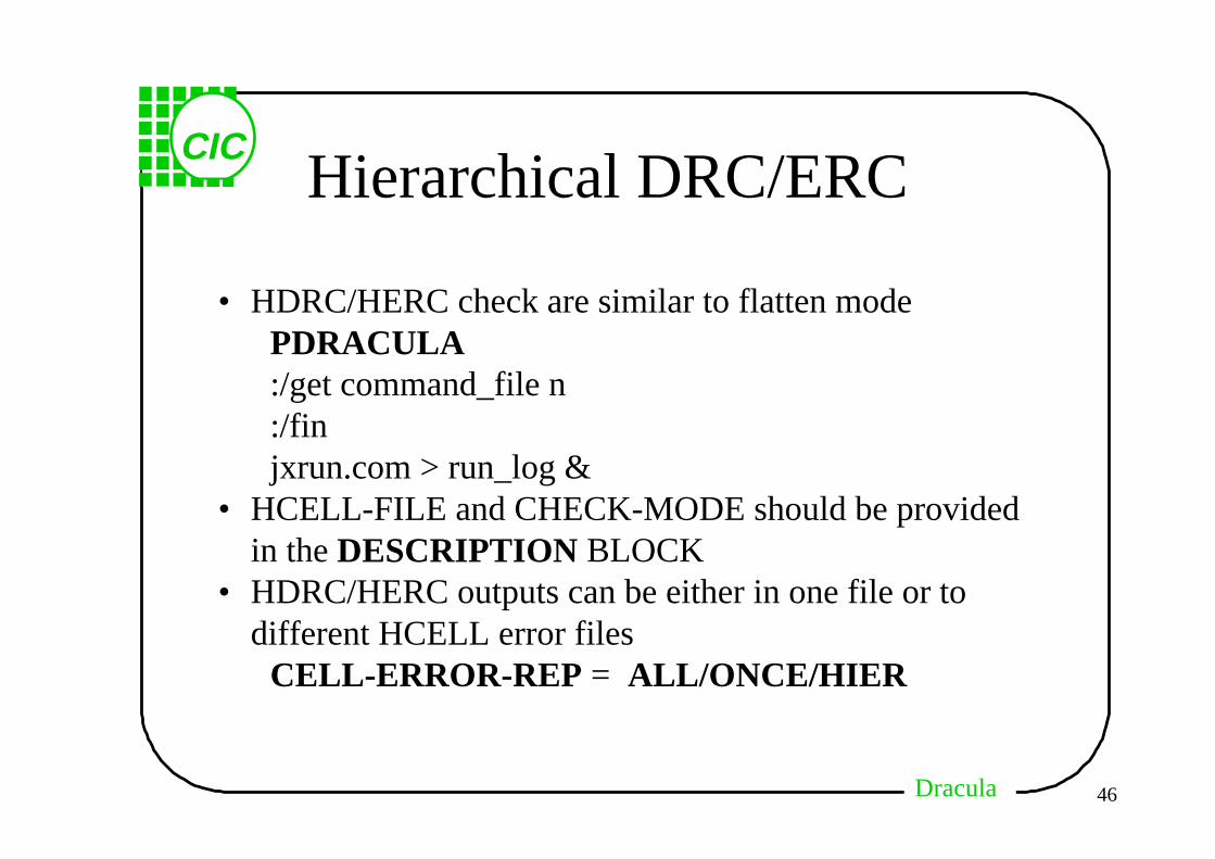
• HDRC/HERC check are similar to flatten modePDRACULA:/get command_file n:/finjxrun.com > run_log &
• HCELL-FILE and CHECK-MODE should be providedin the DESCRIPTION BLOCK
• HDRC/HERC outputs can be either in one file or todifferent HCELL error files
CELL-ERROR-REP = ALL/ONCE/HIER
DraculaDracula
CIC
47
Preparing Netlist• µ@LVSÇò�º�� netlist �
• �¿netlist�H¸SPICE�ëCDL�ÿverilog (û
• SPICE/CDL �<�ÞSUBCKTÊ÷Ä
• µ@LVSÇòënetlist ��ºíLOGLVSinterpret
• c�OPUSÇCDL OUT�ë 5f7analog deviceë�ÒÊ– setenv CDS_Netlisting_Mode Analog
DraculaDracula
CIC
48
Control statement of Netlist file
'‘ * ’ ÉÇ�statement»�¿¸FDracula��'‘ $ ’ÉÇ�statement»�¿¸comment,DraculaÃ��
*.GLOBAL (0�global node) (ex)*.GLOBAL VDD,VSS*.BIPOLAR ( �statement LOGLVS �ÜenetlistÄ� R,C,diode'Y�ð�,´ü���Ô ��command fileá ãð�Ø°Ê÷)O�*.BIPOLAR H:
*.RESVAL *.RESSIZE (YR valuesize check)*.CAPVAL *.CAPAREA (YC valuearea check)*.DIOAREA *.DIOPERI (Ydiode areaperimeter check)
*.UNSPEC_MOS ( �statement,õ´netlistÄûgÊW,L�,�show message$‘PRINT.OUT’Ä*.REVERSE(LOGLVS��MOSྸW,L, MOSྸL,W�H��statement)
Preparing Netlist
DraculaDracula
CIC
49
LOGLVS
:htv:genpad
:case:cir artchip.cdl:ver verilog.v:con artchip:exit
Error file: PRINT.OUT(log file)Translation table:IMAGE.LIS(all of the net-names)
generate information for inquerygenerate a 6gpads.dat file for LVSdevice reductionspecify case sensitivityread the spice/cdl netlistread verilog fileconvert from the top cell name
LOGLVS
DraculaDracula
CIC
50
LVS Command FileINDISK = amp1.db ; GDSII Layout Database FileNamePRIMARY = amp1 ; Chip Top Cell NameOUTDISK = amp1.out ; GDSII Output Filename of ErrorPRINTFILE = amp1 ; Root Name of Text Output FilenameSYSTEM = GDS2 ; Layout Database FormatLISTERROR = YES ; print the X, Y coordinate of the error flagsKEEPDATA = SMART ; Delete intermediate data files during the runTEXT-PRI-ONLY = YES ; Use top level text for node name; TEXT-LEVEL = 1 ; Specify the level of text for extractionFLAG-SELFINTERS = YES ; report polygons with edges self-intersectERROR-PATH-WIDTH = 5.0 MIC ; Width of Error FlagSCHEMATIC = LVSLOGIC ; Compiles netlist generated by LOGLVSABORT-P-G-SHORT = YES *OPERATIONEDTEXT=TEXT.FILEELEMENT CAP[CP] CAPT CPOLYC GPOLYCPARAMETER CAP[CP] 6.495E-16ELEMENT MOS[NM] NGATE GPOLYC NDIFFC PSUB;****** LVS CHECKING **********LVSCHK[SCRA] WPERCENT=1 LPERCENT=1 CAPVAL=5*END
DraculaDracula
CIC
51
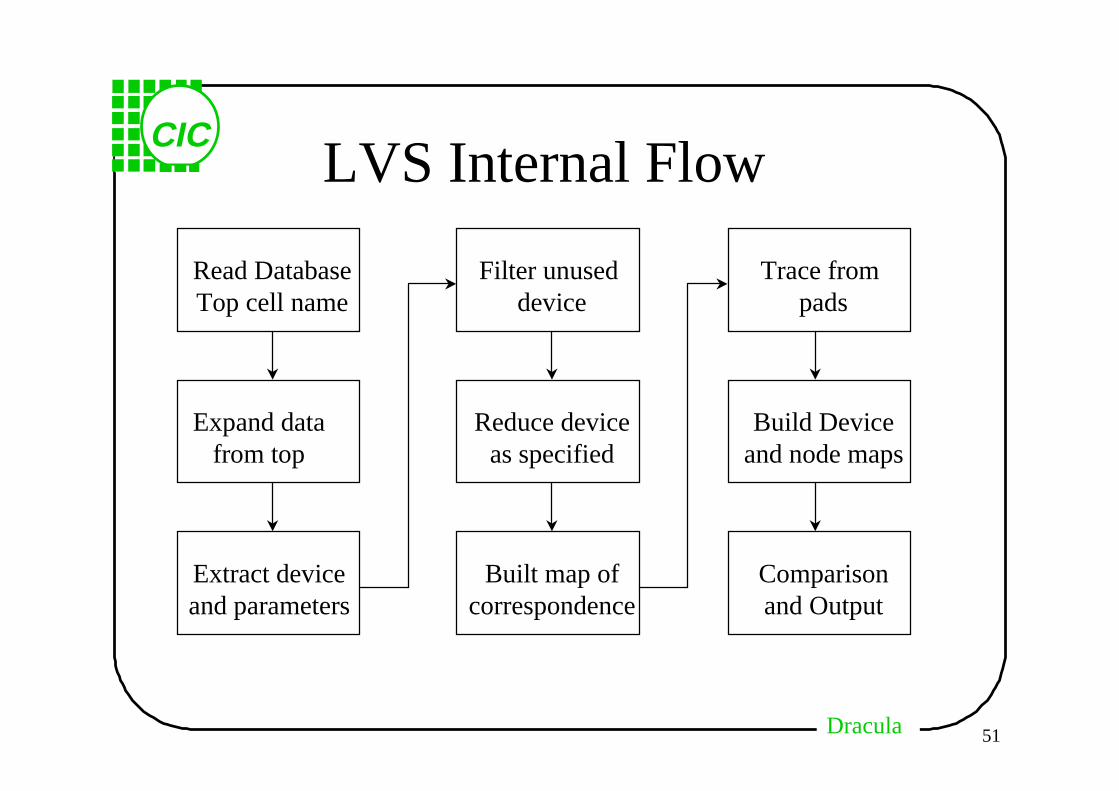
LVS Internal Flow
Read DatabaseTop cell name
Expand datafrom top
Extract deviceand parameters
Filter unused device
Reduce deviceas specified
Built map ofcorrespondence
Trace from pads
Build Deviceand node maps
Comparisonand Output
DraculaDracula
CIC
52
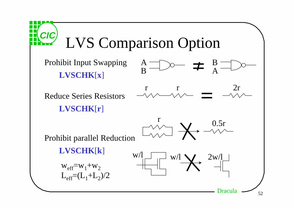
LVS Comparison OptionProhibit Input Swapping A
BLVSCHK [x] AB
Reduce Series Resistors
Prohibit parallel Reduction
r r 2r
LVSCHK [r ]r 0.5r
LVSCHK [k] w/l w/l 2w/lweff=w1+w2
Leff=(L1+L2)/2
DraculaDracula
CIC
53
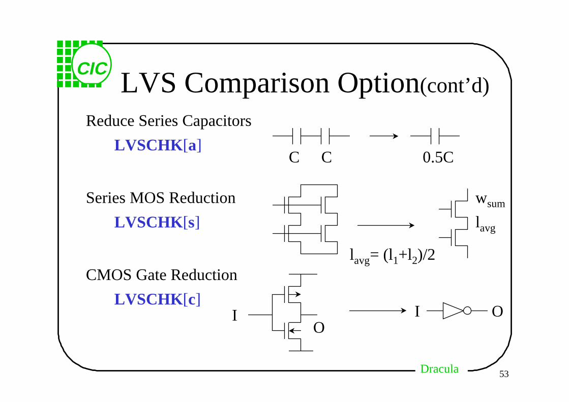
LVS Comparison Option(cont’d)
Series MOS Reduction
LVSCHK [s]
Reduce Series Capacitors
CMOS Gate Reduction
LVSCHK [a]
LVSCHK [c]
C C 0.5C
IO
I O
wsum
lavg
lavg= (l1+l2)/2
DraculaDracula
CIC
54
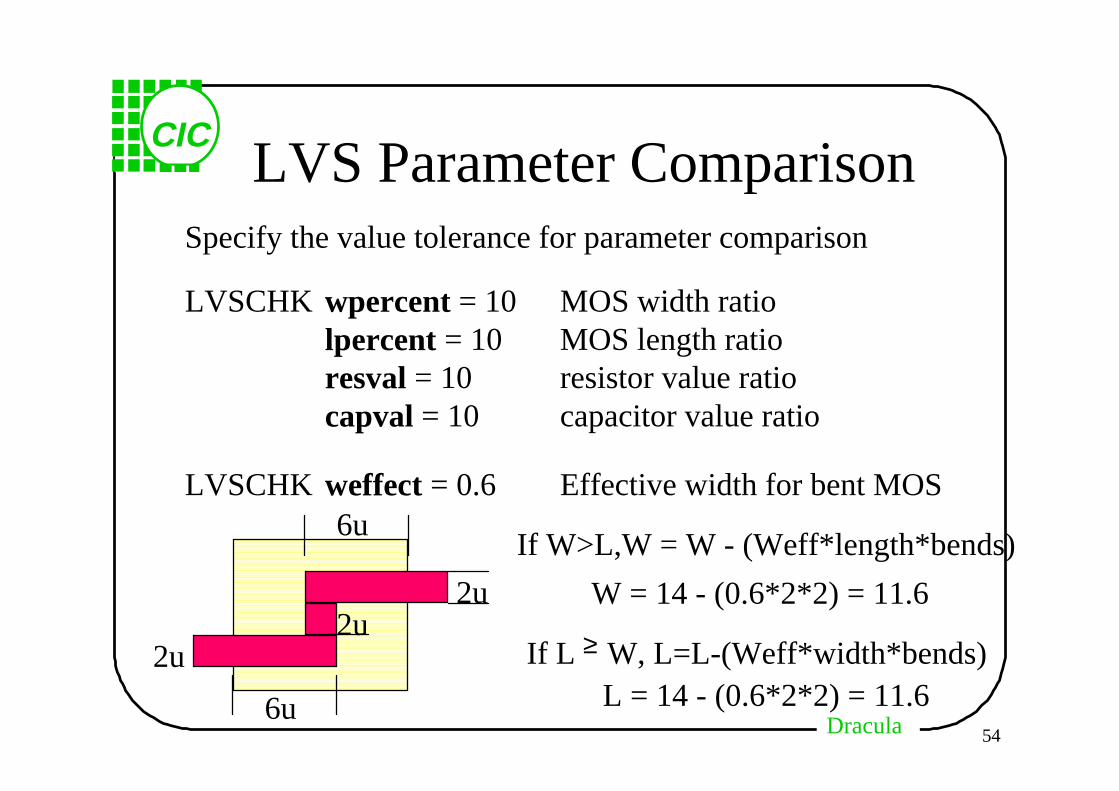
LVS Parameter ComparisonSpecify the value tolerance for parameter comparison
LVSCHK wpercent = 10 lpercent = 10resval = 10capval = 10
MOS width ratio MOS length ratioresistor value ratiocapacitor value ratio
LVSCHK weffect = 0.6 Effective width for bent MOS6u
6u
2u
2u2u
If W>L,W = W - (Weff*length*bends)
W = 14 - (0.6*2*2) = 11.6
If L W, L=L-(Weff*width*bends)≥
L = 14 - (0.6*2*2) = 11.6
DraculaDracula
CIC
55
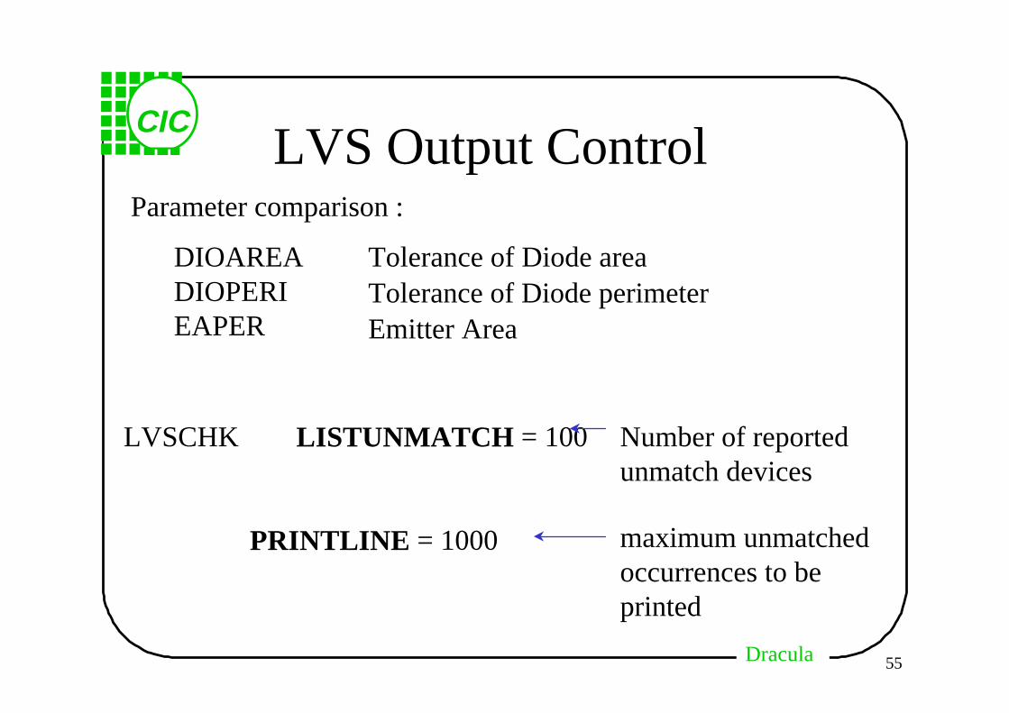
LVS Output Control
LVSCHK LISTUNMATCH = 100
PRINTLINE = 1000
Number of reported unmatch devices
maximum unmatchedoccurrences to beprinted
Parameter comparison :
DIOAREADIOPERIEAPER
Tolerance of Diode areaTolerance of Diode perimeterEmitter Area
DraculaDracula
CIC
56
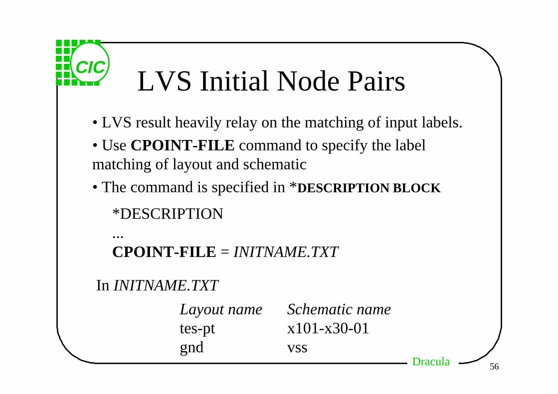
LVS Initial Node Pairs• LVS result heavily relay on the matching of input labels.
• Use CPOINT-FILE command to specify the labelmatching of layout and schematic
• The command is specified in *DESCRIPTION BLOCK
*DESCRIPTION...CPOINT-FILE = INITNAME.TXT
In INITNAME.TXT
Layout name tes-ptgnd
Schematic namex101-x30-01vss
DraculaDracula
CIC
57
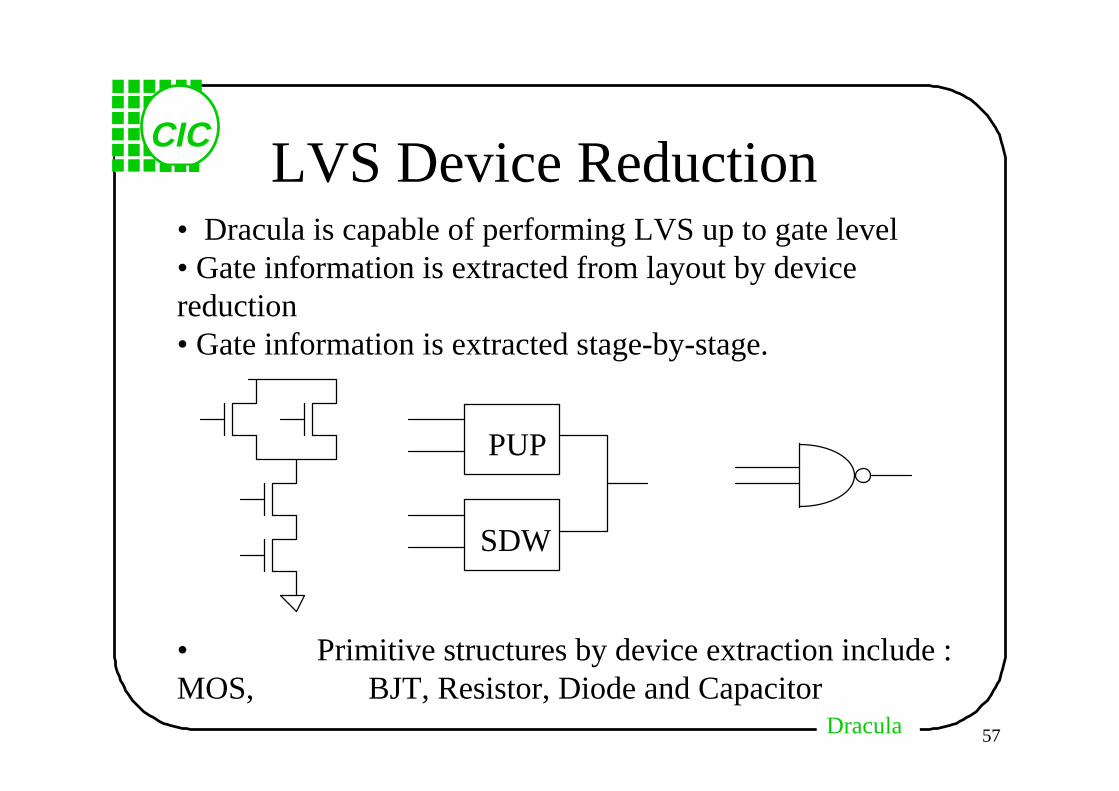
LVS Device Reduction• Dracula is capable of performing LVS up to gate level• Gate information is extracted from layout by device reduction• Gate information is extracted stage-by-stage.
• Primitive structures by device extraction include :MOS, BJT, Resistor, Diode and Capacitor
PUP
SDW
DraculaDracula
CIC
58
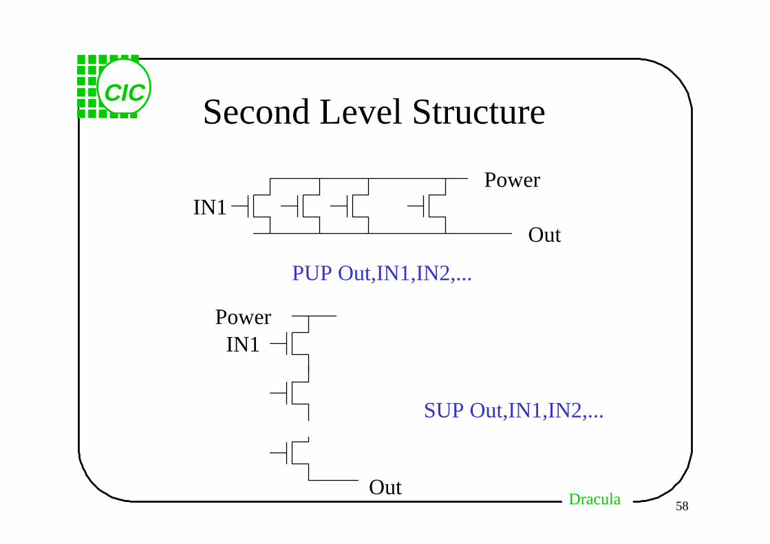
Second Level Structure
Power
Out
PUP Out,IN1,IN2,...
Power
IN1
IN1
Out
SUP Out,IN1,IN2,...
DraculaDracula
CIC
59
Second Level Structure(cont’d)
Ground
Out
PDW Out,IN1,IN2,...
Ground
IN1
IN1
SDW Out,IN1,IN2,...
Out
DraculaDracula
CIC
60
Second Level Structure(cont’d)
Vdd
Out
PUPI out1,IN1,IN2
SUP Out,IN3,out1
SDWI out2,IN1,IN2
PDW Out,IN3,out2
IN1IN2
IN3
Out
PUPI
SDWI SUPPDW
AOI Gate
Incomplete
DraculaDracula
CIC
61
Main Body LVS Report
• Execution time and run options
• Initial Correspondence Node PairsList the node pairs given by user
• Correspondence Node PairsLists the node mapping by DRACULA
• Device Match Summary -> unmatched device = 0 Reports the number of matched/unmatched device
• Discrepancy Points ListingList detailed examination of 15 error types
• Detailed Device Matching SummaryList all unmatched devices by device type
DraculaDracula
CIC
62
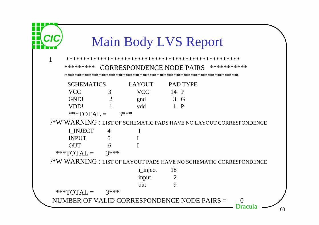
Main Body LVS Report ***************** LVS REPORT ***************** DATE : 21-MAY-97 TIME : 17:04:29 PRINTLINE = 1000 MOS DEVICE WIDTH NOT CHECKED MOS DEVICE LENGTH NOT CHECKED UNSPECIFIED SCHEMATICAL PARAMETERS ARE CONSIDERED AS MISMATCH UNSPECIFIED SCHEMATICAL SUBSTRATES ARE CONSIDERED AS MISMATCH UNSPECIFIED LAYOUT PARAMETERS ARE CONSIDERED AS MISMATCH UNSPECIFIED LAYOUT SUBSTRATES ARE CONSIDERED AS MISMATCH
READING CPOINT-FILE FOR INITIAL CORRESPONDENCE POINTS
/*W : SCH. PAD VDD! MATCHED TO LAY. PAD VDD BY PADTYPE /*W : SCH. PAD GND! MATCHED TO LAY. PAD VSS BY PADTYPE
DraculaDracula
CIC
63
Main Body LVS Report1 *************************************************** ********* CORRESPONDENCE NODE PAIRS *********** *************************************************** SCHEMATICS LAYOUT PAD TYPE VCC 3 VCC 14 P GND! 2 gnd 3 G VDD! 1 vdd 1 P ***TOTAL = 3*** /*W WARNING : LIST OF SCHEMATIC PADS HAVE NO LAYOUT CORRESPONDENCE
I_INJECT 4 I INPUT 5 I OUT 6 I ***TOTAL = 3*** /*W WARNING : LIST OF LAYOUT PADS HAVE NO SCHEMATIC CORRESPONDENCE
i_inject 18 input 2 out 9
***TOTAL = 3*** NUMBER OF VALID CORRESPONDENCE NODE PAIRS = 0
DraculaDracula
CIC
64
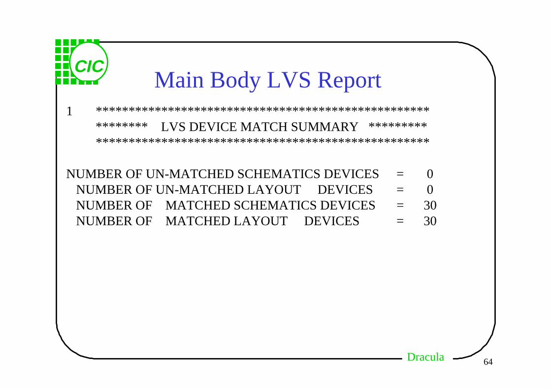
Main Body LVS Report1 *************************************************** ******** LVS DEVICE MATCH SUMMARY ********* *************************************************** NUMBER OF UN-MATCHED SCHEMATICS DEVICES = 0 NUMBER OF UN-MATCHED LAYOUT DEVICES = 0 NUMBER OF MATCHED SCHEMATICS DEVICES = 30 NUMBER OF MATCHED LAYOUT DEVICES = 30
DraculaDracula
CIC
65
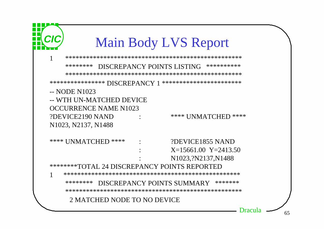
Main Body LVS Report1 *************************************************** ******** DISCREPANCY POINTS LISTING ********** ******************************************************************* DISCREPANCY 1 ***********************-- NODE N1023-- WTH UN-MATCHED DEVICEOCCURRENCE NAME N1023?DEVICE2190 NAND : **** UNMATCHED ****N1023, N2137, N1488
**** UNMATCHED **** : ?DEVICE1855 NAND: X=15661.00 Y=2413.50: N1023,?N2137,N1488
********TOTAL 24 DISCREPANCY POINTS REPORTED 1 *************************************************** ******** DISCREPANCY POINTS SUMMARY ******* ***************************************************
2 MATCHED NODE TO NO DEVICE
DraculaDracula
CIC
66
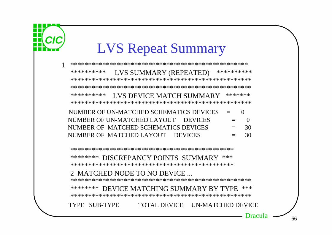
LVS Repeat Summary1 ************************************************** ********** LVS SUMMARY (REPEATED) ********** *************************************************** *************************************************** ********** LVS DEVICE MATCH SUMMARY ******* *************************************************** NUMBER OF UN-MATCHED SCHEMATICS DEVICES = 0 NUMBER OF UN-MATCHED LAYOUT DEVICES = 0 NUMBER OF MATCHED SCHEMATICS DEVICES = 30 NUMBER OF MATCHED LAYOUT DEVICES = 30
********************************************** ******** DISCREPANCY POINTS SUMMARY *** ********************************************** 2 MATCHED NODE TO NO DEVICE ... *************************************************** ******** DEVICE MATCHING SUMMARY BY TYPE *** *************************************************** TYPE SUB-TYPE TOTAL DEVICE UN-MATCHED DEVICE
DraculaDracula
CIC
67
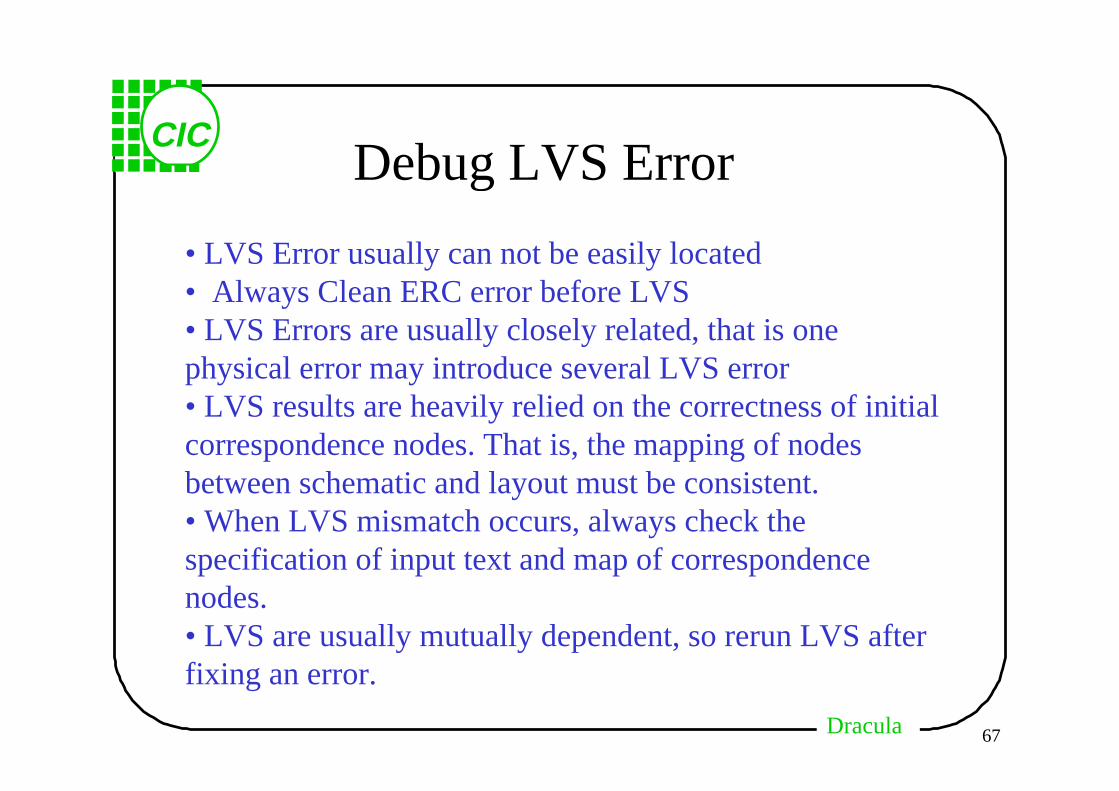
Debug LVS Error
• LVS Error usually can not be easily located• Always Clean ERC error before LVS• LVS Errors are usually closely related, that is one physical error may introduce several LVS error• LVS results are heavily relied on the correctness of initial correspondence nodes. That is, the mapping of nodes between schematic and layout must be consistent.• When LVS mismatch occurs, always check the specification of input text and map of correspondence nodes.• LVS are usually mutually dependent, so rerun LVS after fixing an error.
DraculaDracula
CIC
68
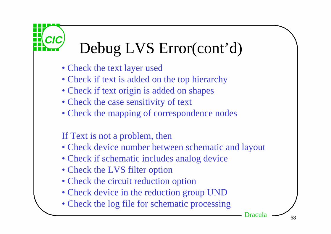
Debug LVS Error(cont’d)• Check the text layer used• Check if text is added on the top hierarchy• Check if text origin is added on shapes• Check the case sensitivity of text• Check the mapping of correspondence nodes
If Text is not a problem, then• Check device number between schematic and layout• Check if schematic includes analog device• Check the LVS filter option• Check the circuit reduction option• Check device in the reduction group UND• Check the log file for schematic processing
DraculaDracula
CIC
69
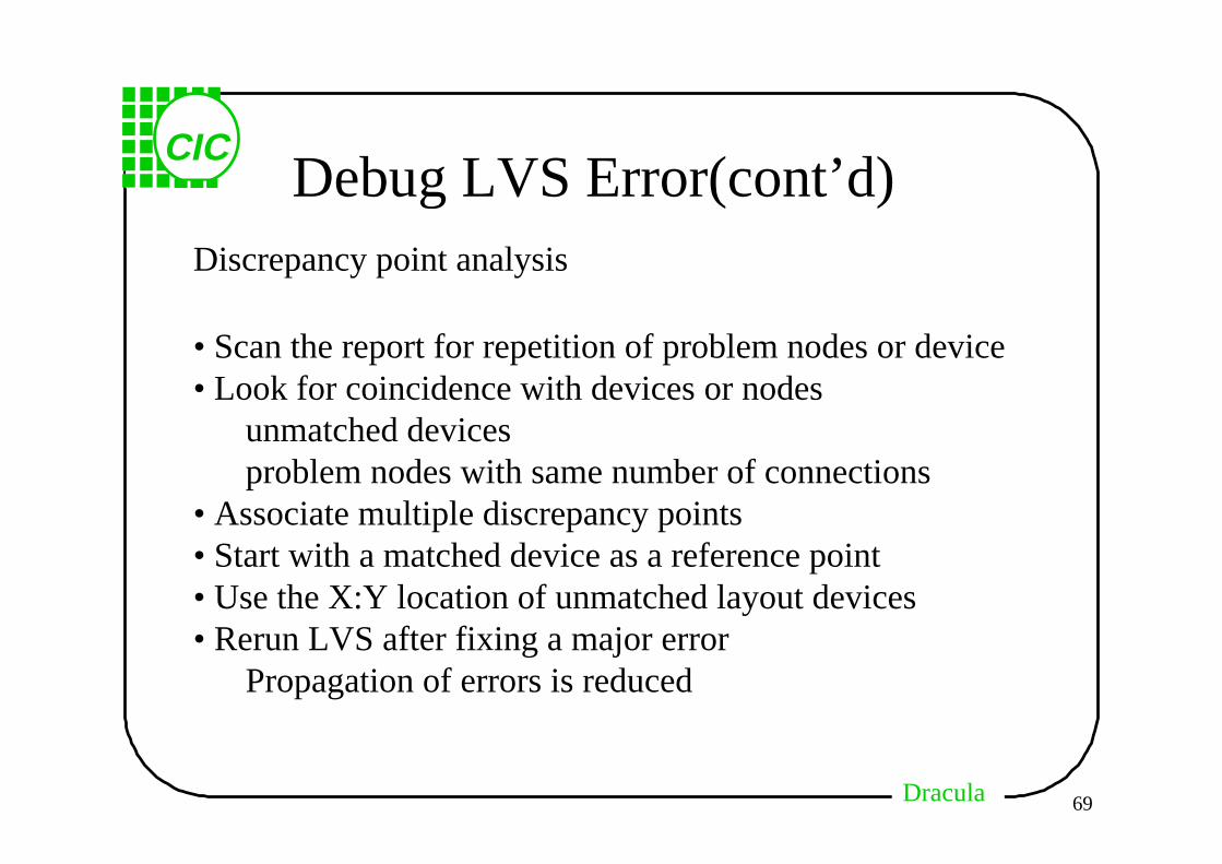
Debug LVS Error(cont’d)Discrepancy point analysis
• Scan the report for repetition of problem nodes or device• Look for coincidence with devices or nodes
unmatched devicesproblem nodes with same number of connections
• Associate multiple discrepancy points• Start with a matched device as a reference point• Use the X:Y location of unmatched layout devices• Rerun LVS after fixing a major error
Propagation of errors is reduced
DraculaDracula
CIC
70
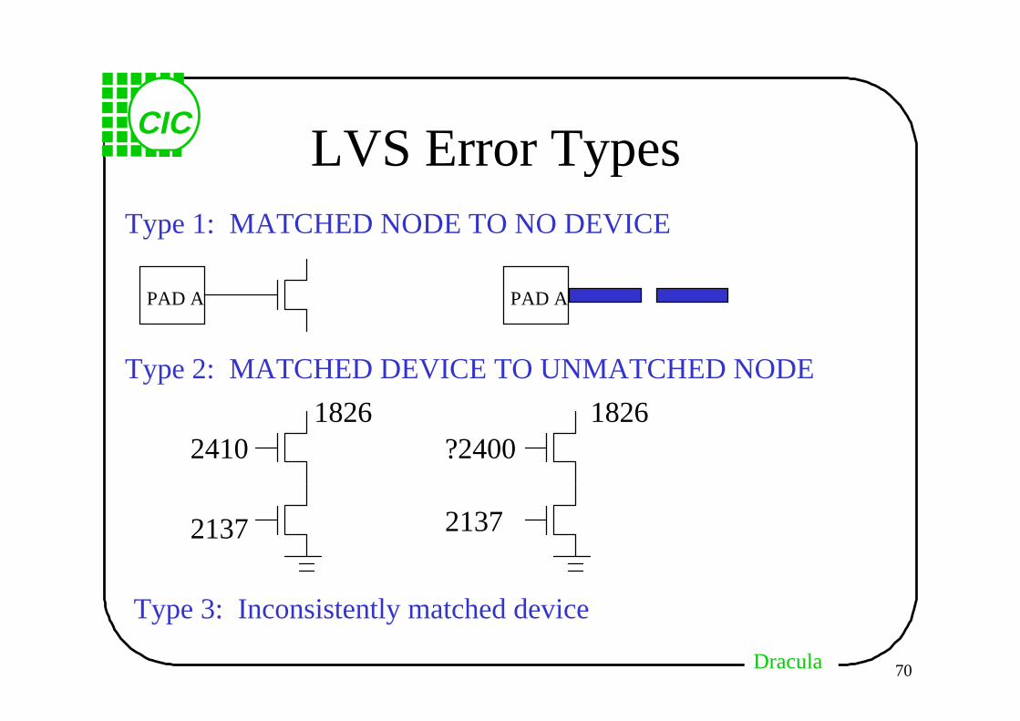
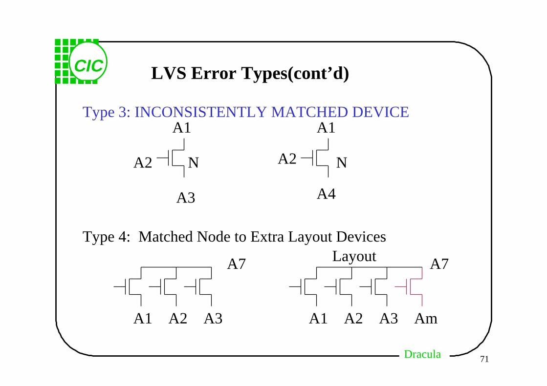
LVS Error TypesType 1: MATCHED NODE TO NO DEVICE
PAD A PAD A
Type 2: MATCHED DEVICE TO UNMATCHED NODE
2137 2137
2410 ?24001826 1826
Type 3: Inconsistently matched device
DraculaDracula
CIC
71
LVS Error Types(cont’d)
Type 3: INCONSISTENTLY MATCHED DEVICE
N N
A1
A2
A3
A1
A2
A4
Type 4: Matched Node to Extra Layout Devices
A7 A7
A1 A2 A3 A1 A2 A3 Am
Layout
DraculaDracula
CIC
72
LVS Error Types(cont’d)
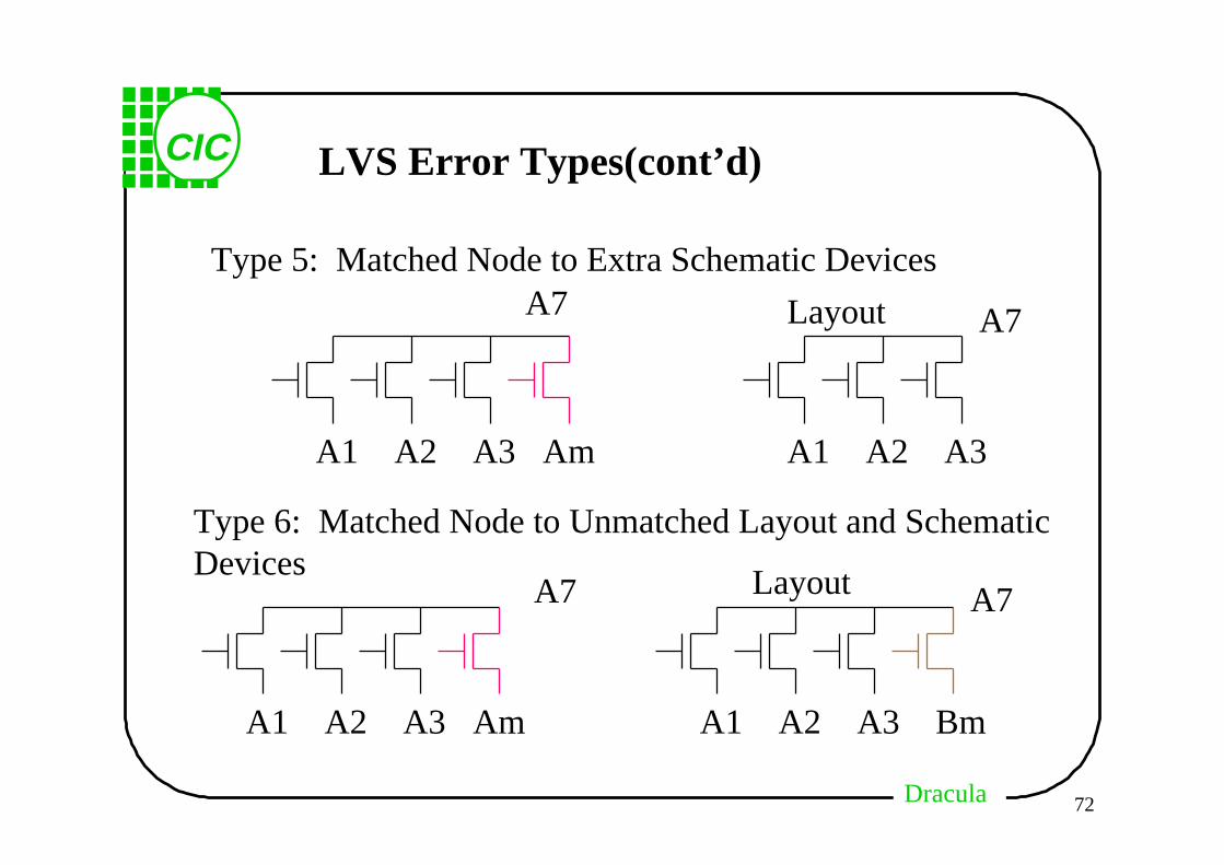
Type 5: Matched Node to Extra Schematic DevicesA7 A7
A1 A2 A3 A1 A2 A3Am
Layout
Type 6: Matched Node to Unmatched Layout and SchematicDevices
A7
A1 A2 A3 Am
A7
A1 A2 A3 Bm
Layout
DraculaDracula
CIC
73
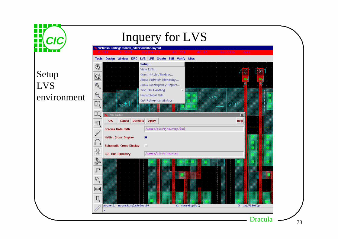
Inquery for LVS
Setup LVSenvironment
DraculaDracula
CIC
74
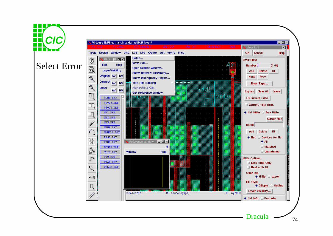
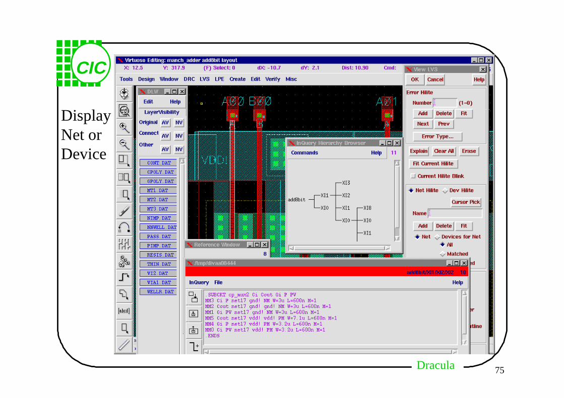
Select Error
DraculaDracula
CIC
75
DisplayNet orDevice
DraculaDracula
CIC
76
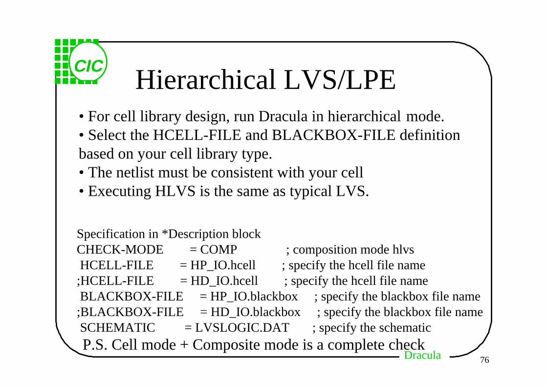
Hierarchical LVS/LPE
Specification in *Description block CHECK-MODE = COMP ; composition mode hlvs HCELL-FILE = HP_IO.hcell ; specify the hcell file name;HCELL-FILE = HD_IO.hcell ; specify the hcell file name BLACKBOX-FILE = HP_IO.blackbox ; specify the blackbox file name;BLACKBOX-FILE = HD_IO.blackbox ; specify the blackbox file name SCHEMATIC = LVSLOGIC.DAT ; specify the schematic
• For cell library design, run Dracula in hierarchical mode.• Select the HCELL-FILE and BLACKBOX-FILE definitionbased on your cell library type.• The netlist must be consistent with your cell• Executing HLVS is the same as typical LVS.
P.S. Cell mode + Composite mode is a complete check
DraculaDracula
CIC
77
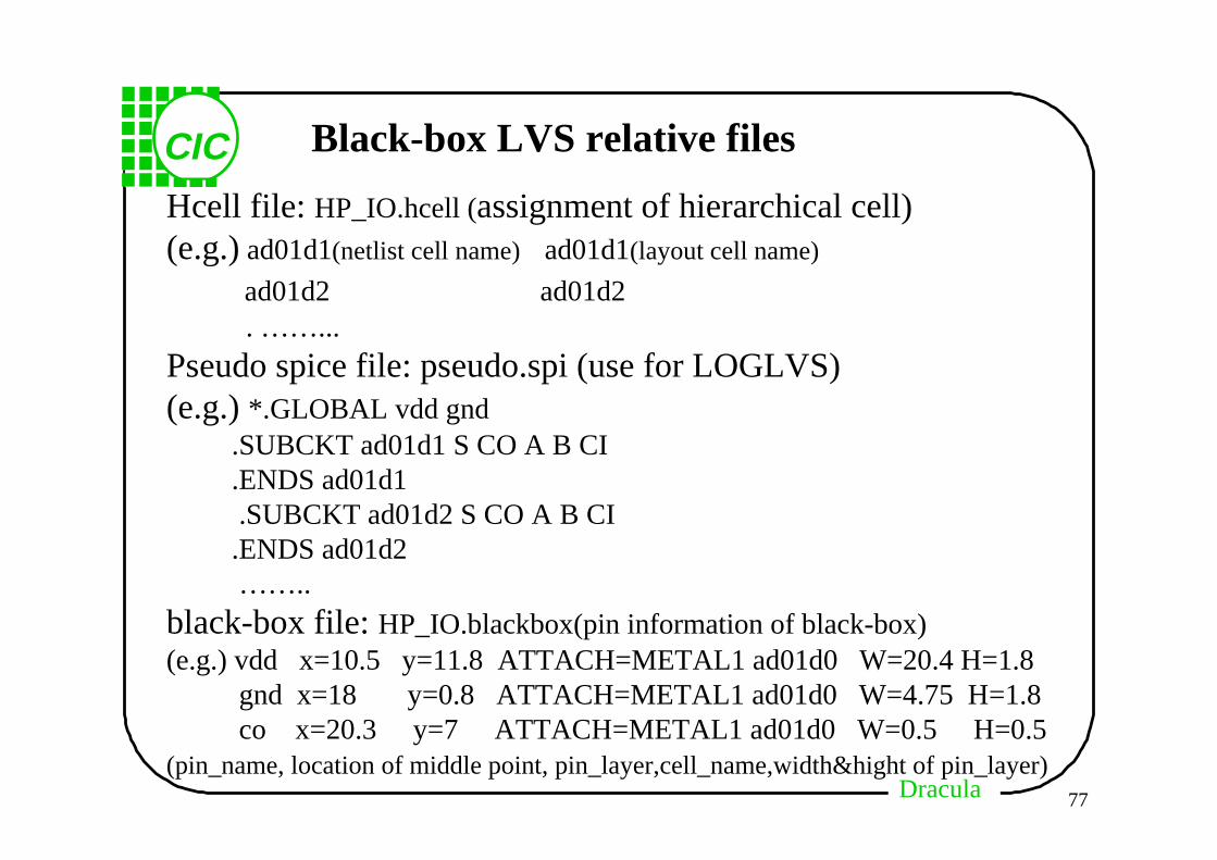
Black-box LVS relative files
Hcell file: HP_IO.hcell (assignment of hierarchical cell)(e.g.) ad01d1(netlist cell name) ad01d1(layout cell name)
ad01d2 ad01d2 . ……...Pseudo spice file: pseudo.spi (use for LOGLVS)(e.g.) *.GLOBAL vdd gnd .SUBCKT ad01d1 S CO A B CI .ENDS ad01d1 .SUBCKT ad01d2 S CO A B CI .ENDS ad01d2 ……..black-box file: HP_IO.blackbox(pin information of black-box)(e.g.) vdd x=10.5 y=11.8 ATTACH=METAL1 ad01d0 W=20.4 H=1.8 gnd x=18 y=0.8 ATTACH=METAL1 ad01d0 W=4.75 H=1.8 co x=20.3 y=7 ATTACH=METAL1 ad01d0 W=0.5 H=0.5(pin_name, location of middle point, pin_layer,cell_name,width&hight of pin_layer)
DraculaDracula
CIC
78
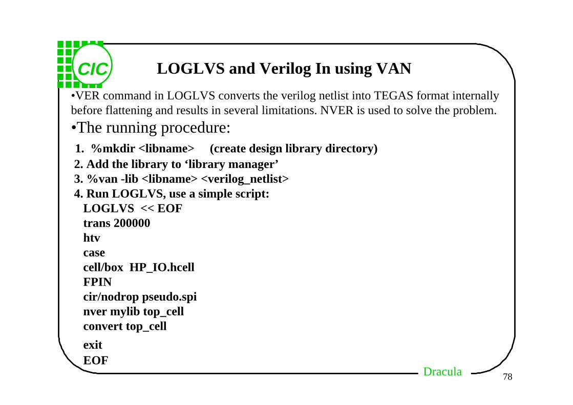
LOGLVS and Verilog In using VAN
•VER command in LOGLVS converts the verilog netlist into TEGAS format internallybefore flattening and results in several limitations. NVER is used to solve the problem.
•The running procedure: 1. %mkdir <libname> (create design library directory) 2. Add the library to ‘library manager’ 3. %van -lib <libname> <verilog_netlist> 4. Run LOGLVS, use a simple script: LOGLVS << EOF trans 200000 htv case cell/box HP_IO.hcell FPIN cir/nodrop pseudo.spi nver mylib top_cell convert top_cell
exit EOF
DraculaDracula
CIC
79
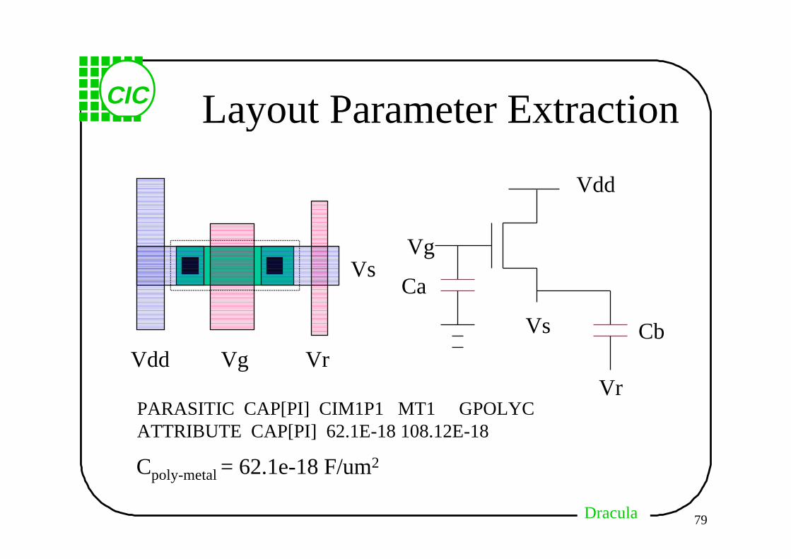
Layout Parameter Extraction
Vdd Vg
Vs
Vr
Vg
Vdd
Vs
Vr
Ca
Cb
Cpoly-metal = 62.1e-18 F/um2
PARASITIC CAP[PI] CIM1P1 MT1 GPOLYC ATTRIBUTE CAP[PI] 62.1E-18 108.12E-18
DraculaDracula
CIC
80
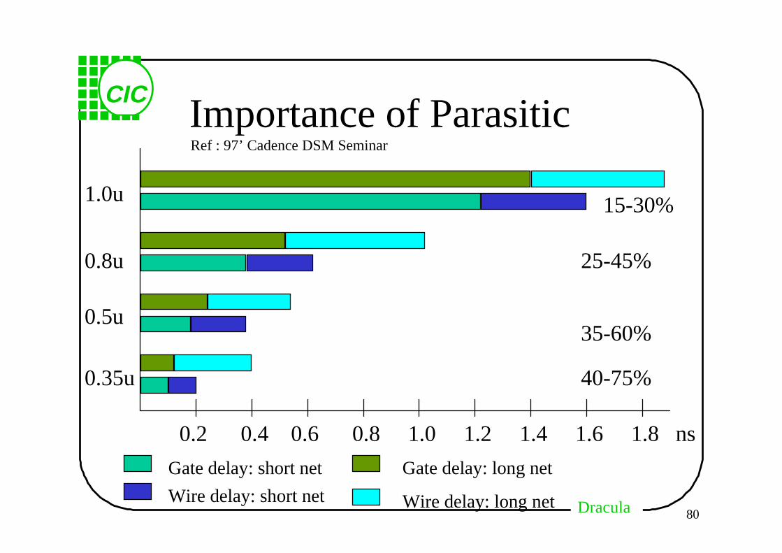
Importance of Parasitic
0.2 0.4 0.6 0.8 1.0 1.2 1.4 1.6 1.8 ns
1.0u
0.8u
0.5u
0.35u
Gate delay: short net Gate delay: long net
Wire delay: short net Wire delay: long net
40-75%
35-60%
25-45%
15-30%
Ref : 97’ Cadence DSM Seminar
DraculaDracula
CIC
81
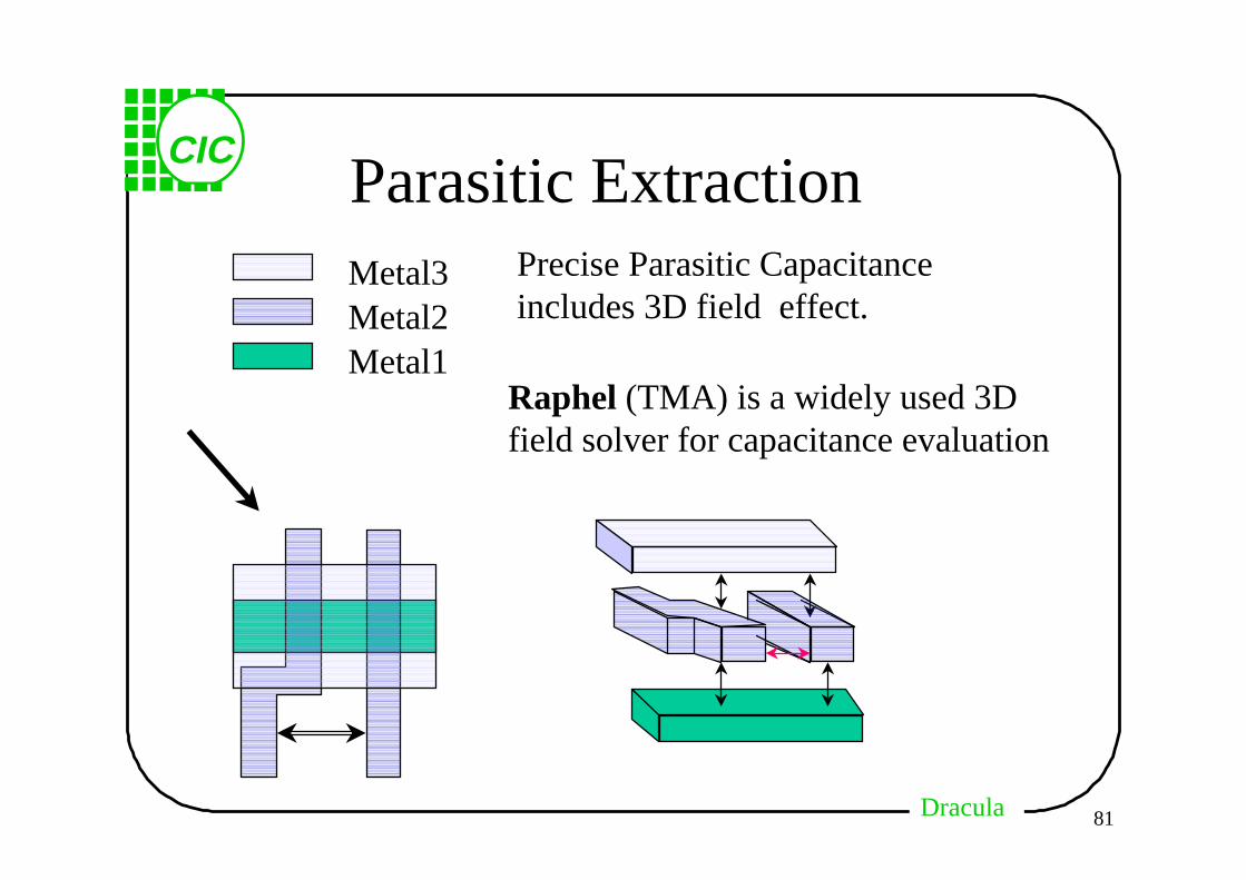
Parasitic ExtractionMetal3Metal2Metal1
Precise Parasitic Capacitanceincludes 3D field effect.
Raphel (TMA) is a widely used 3Dfield solver for capacitance evaluation
DraculaDracula
CIC
82
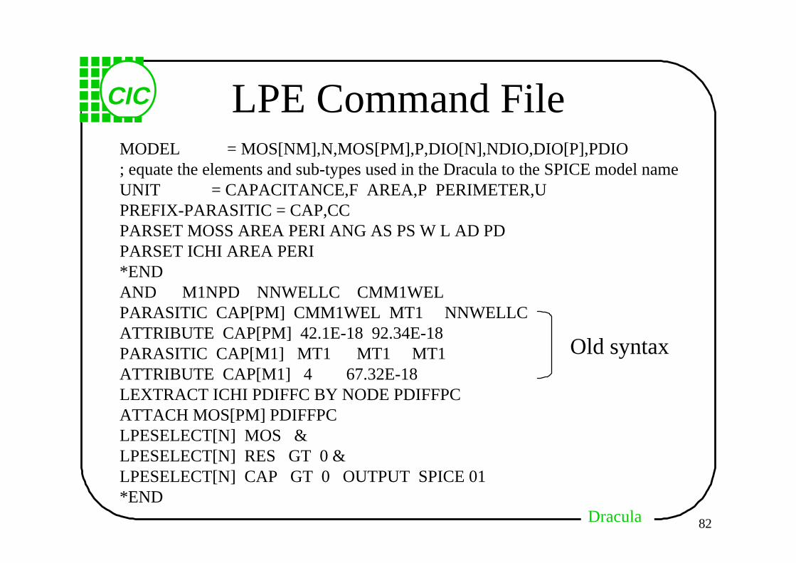
LPE Command FileMODEL = MOS[NM],N,MOS[PM],P,DIO[N],NDIO,DIO[P],PDIO; equate the elements and sub-types used in the Dracula to the SPICE model nameUNIT = CAPACITANCE,F AREA,P PERIMETER,UPREFIX-PARASITIC = CAP,CCPARSET MOSS AREA PERI ANG AS PS W L AD PDPARSET ICHI AREA PERI*ENDAND M1NPD NNWELLC CMM1WELPARASITIC CAP[PM] CMM1WEL MT1 NNWELLCATTRIBUTE CAP[PM] 42.1E-18 92.34E-18PARASITIC CAP[M1] MT1 MT1 MT1ATTRIBUTE CAP[M1] 4 67.32E-18LEXTRACT ICHI PDIFFC BY NODE PDIFFPCATTACH MOS[PM] PDIFFPCLPESELECT[N] MOS &LPESELECT[N] RES GT 0 &LPESELECT[N] CAP GT 0 OUTPUT SPICE 01*END
Old syntax
DraculaDracula
CIC
83
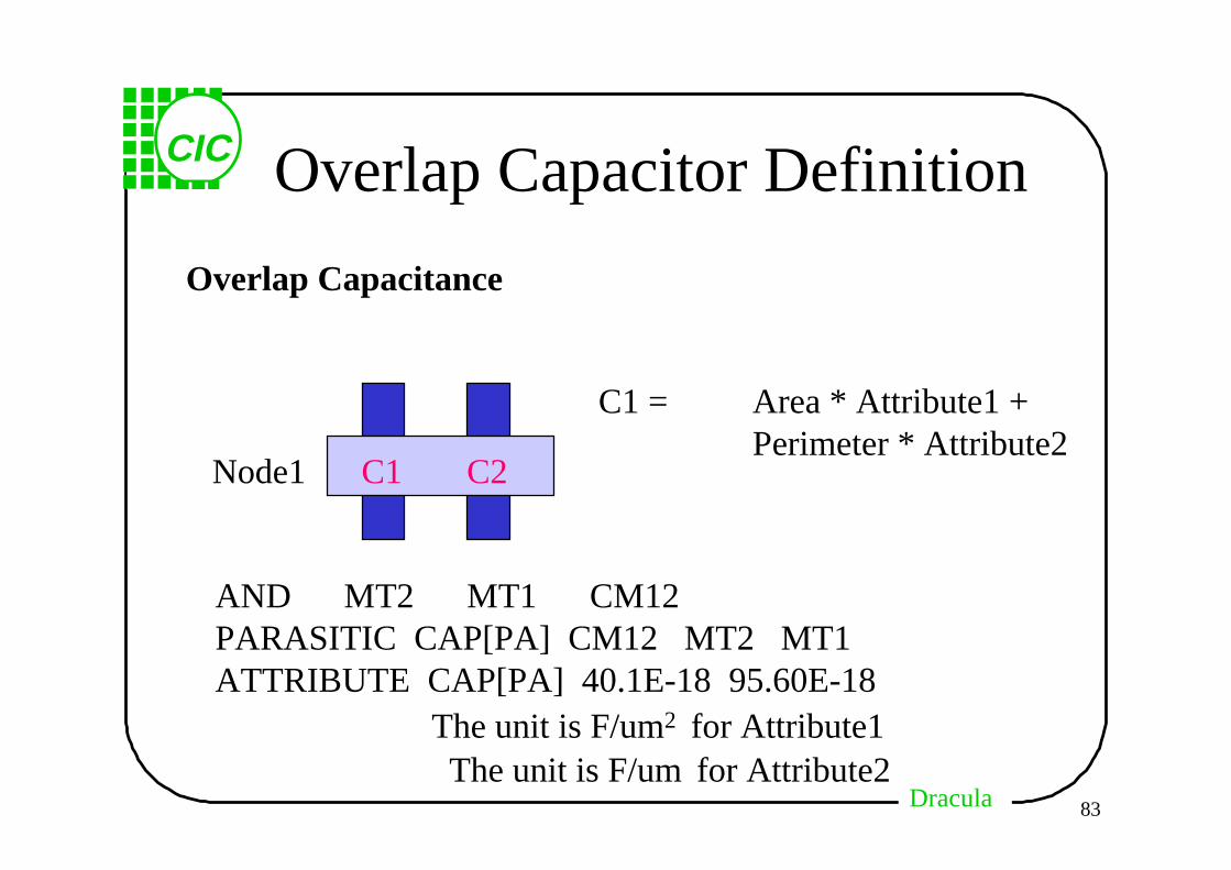
Overlap Capacitor Definition
Overlap Capacitance
C2C1Node1
C1 = Area * Attribute1 +Perimeter * Attribute2
AND MT2 MT1 CM12 PARASITIC CAP[PA] CM12 MT2 MT1 ATTRIBUTE CAP[PA] 40.1E-18 95.60E-18
The unit is F/um2 for Attribute1The unit is F/um for Attribute2
DraculaDracula
CIC
84
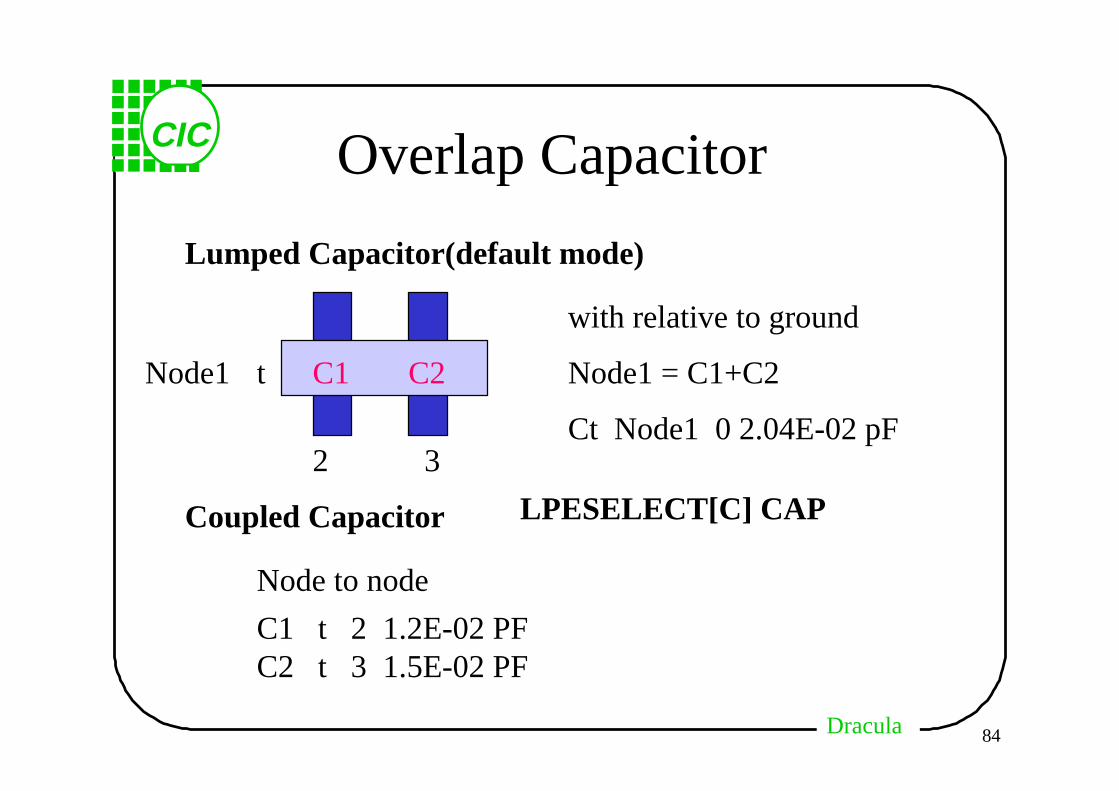
Overlap Capacitor
Node1 = C1+C2
Lumped Capacitor(default mode)
Coupled Capacitor
C2C1Node1
with relative to ground
Node to node
Ct Node1 0 2.04E-02 pF2 3
t
C1 t 2 1.2E-02 PFC2 t 3 1.5E-02 PF
LPESELECT[C] CAP
DraculaDracula
CIC
85
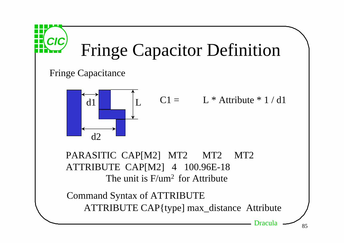
Fringe Capacitor DefinitionFringe Capacitance
d1 L C1 = L * Attribute * 1 / d1
d2
PARASITIC CAP[M2] MT2 MT2 MT2ATTRIBUTE CAP[M2] 4 100.96E-18
The unit is F/um2 for Attribute
Command Syntax of ATTRIBUTEATTRIBUTE CAP{type] max_distance Attribute
DraculaDracula
CIC
86
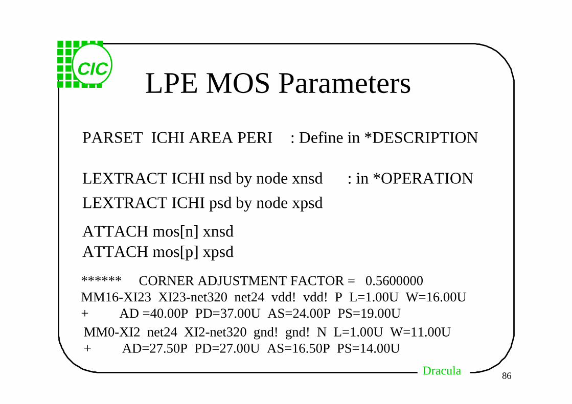
LPE MOS Parameters
PARSET ICHI AREA PERI
LEXTRACT ICHI nsd by node xnsd
ATTACH mos[n] xnsd
LEXTRACT ICHI psd by node xpsd
ATTACH mos[p] xpsd
: Define in *DESCRIPTION
: in *OPERATION
****** CORNER ADJUSTMENT FACTOR = 0.5600000MM16-XI23 XI23-net320 net24 vdd! vdd! P L=1.00U W=16.00U+ AD =40.00P PD=37.00U AS=24.00P PS=19.00UMM0-XI2 net24 XI2-net320 gnd! gnd! N L=1.00U W=11.00U+ AD=27.50P PD=27.00U AS=16.50P PS=14.00U
DraculaDracula
CIC
87
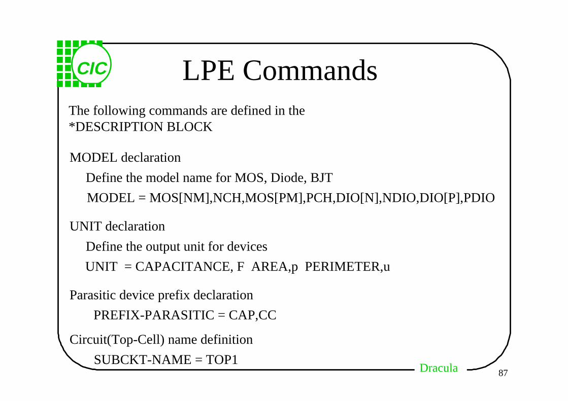
LPE Commands
MODEL declaration
Define the model name for MOS, Diode, BJT
MODEL = MOS[NM],NCH,MOS[PM],PCH,DIO[N],NDIO,DIO[P],PDIO
UNIT declaration
Define the output unit for devices
UNIT = CAPACITANCE, F AREA,p PERIMETER,u
PREFIX-PARASITIC = CAP,CC
Parasitic device prefix declaration
The following commands are defined in the*DESCRIPTION BLOCK
Circuit(Top-Cell) name definition
SUBCKT-NAME = TOP1
DraculaDracula
CIC
88
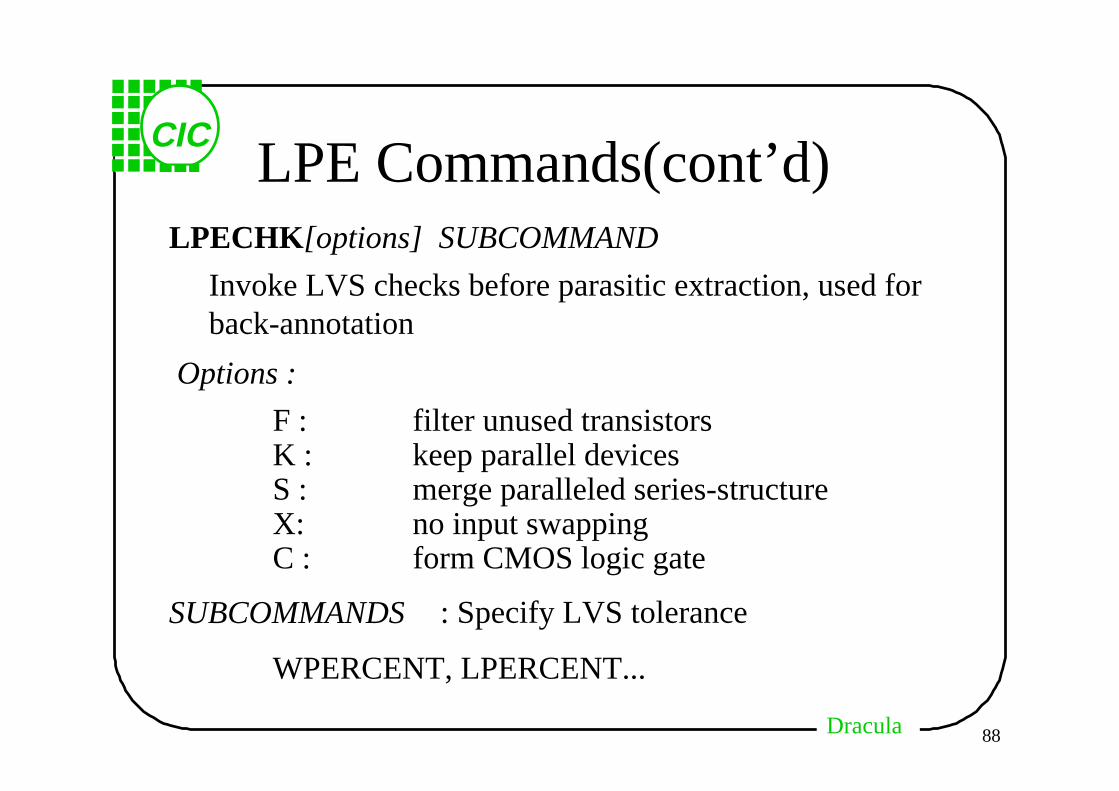
LPE Commands(cont’d)LPECHK [options] SUBCOMMAND
Invoke LVS checks before parasitic extraction, used forback-annotation
Options :
F : filter unused transistorsK : keep parallel devicesS : merge paralleled series-structureX: no input swappingC : form CMOS logic gate
SUBCOMMANDS : Specify LVS tolerance
WPERCENT, LPERCENT...
DraculaDracula
CIC
89
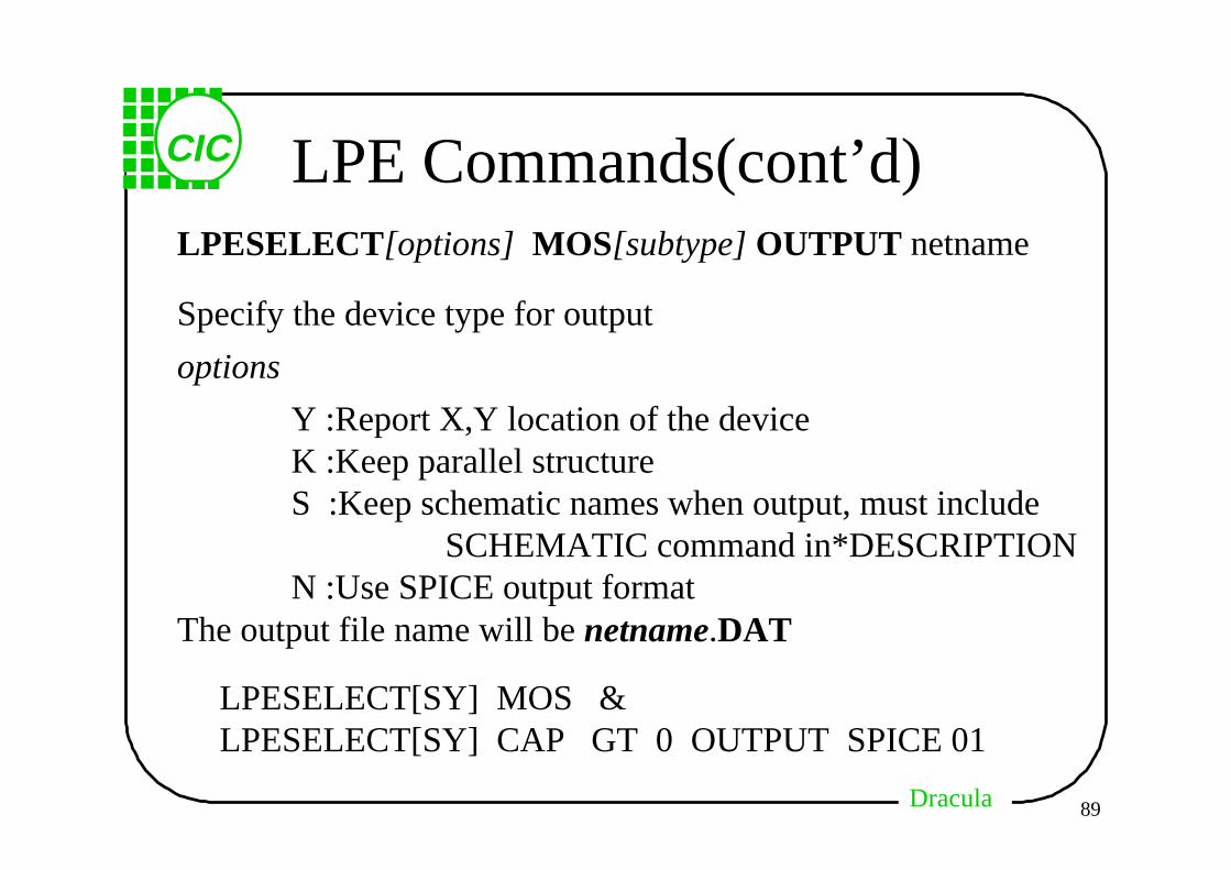
LPE Commands(cont’d)LPESELECT [options] MOS[subtype] OUTPUT netname
Specify the device type for output
options
Y :Report X,Y location of the deviceK :Keep parallel structureS :Keep schematic names when output, must include
SCHEMATIC command in*DESCRIPTIONN :Use SPICE output format
The output file name will be netname.DAT
LPESELECT[SY] MOS & LPESELECT[SY] CAP GT 0 OUTPUT SPICE 01
DraculaDracula
CIC
90
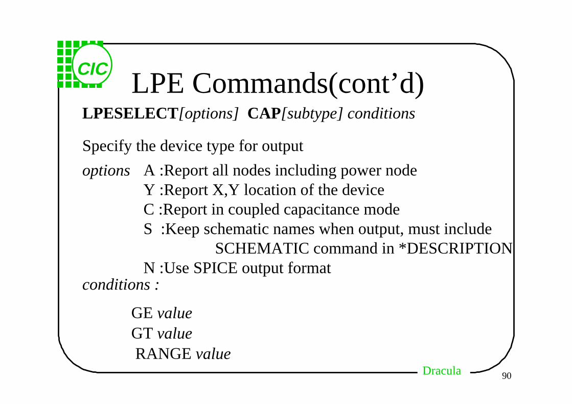
LPE Commands(cont’d)LPESELECT [options] CAP[subtype] conditions
Specify the device type for output
options A :Report all nodes including power nodeY :Report X,Y location of the deviceC :Report in coupled capacitance modeS :Keep schematic names when output, must include
SCHEMATIC command in *DESCRIPTIONN :Use SPICE output format
GE value
conditions :
GT valueRANGE value
DraculaDracula
CIC
91
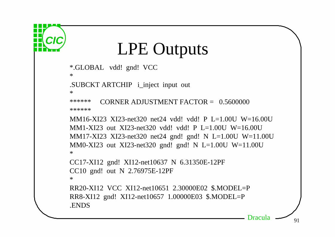
LPE Outputs*.GLOBAL vdd! gnd! VCC*.SUBCKT ARTCHIP i_inject input out******* CORNER ADJUSTMENT FACTOR = 0.5600000******MM16-XI23 XI23-net320 net24 vdd! vdd! P L=1.00U W=16.00UMM1-XI23 out XI23-net320 vdd! vdd! P L=1.00U W=16.00UMM17-XI23 XI23-net320 net24 gnd! gnd! N L=1.00U W=11.00UMM0-XI23 out XI23-net320 gnd! gnd! N L=1.00U W=11.00U*CC17-XI12 gnd! XI12-net10637 N 6.31350E-12PFCC10 gnd! out N 2.76975E-12PF*RR20-XI12 VCC XI12-net10651 2.30000E02 $.MODEL=PRR8-XI12 gnd! XI12-net10657 1.00000E03 $.MODEL=P.ENDS
DraculaDracula
CIC
92
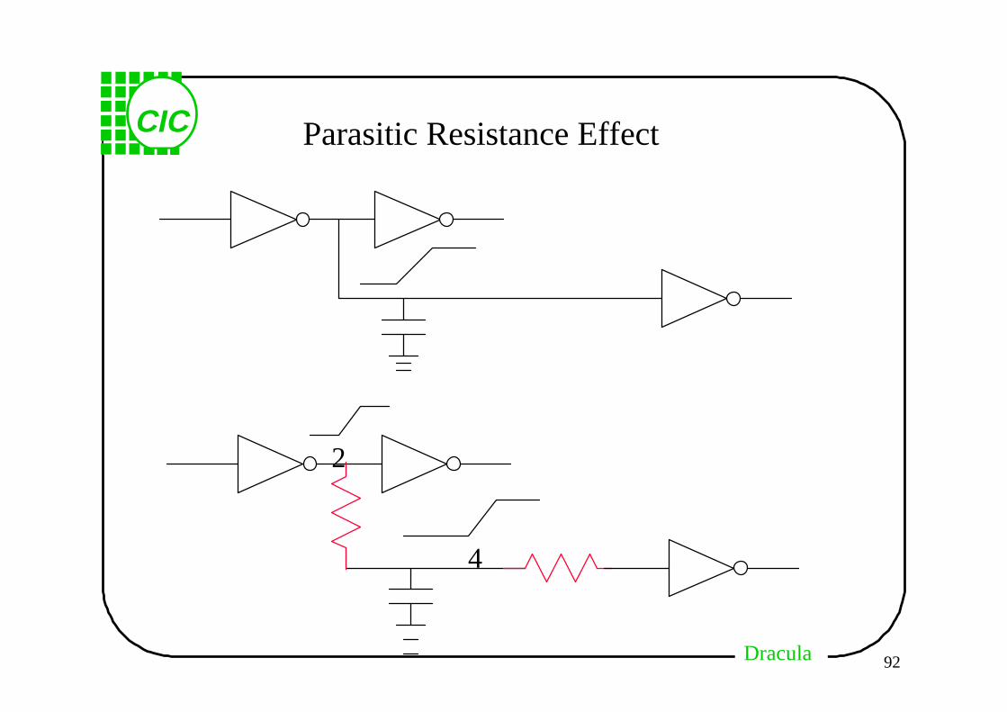
Parasitic Resistance Effect
2
4
DraculaDracula
CIC
93
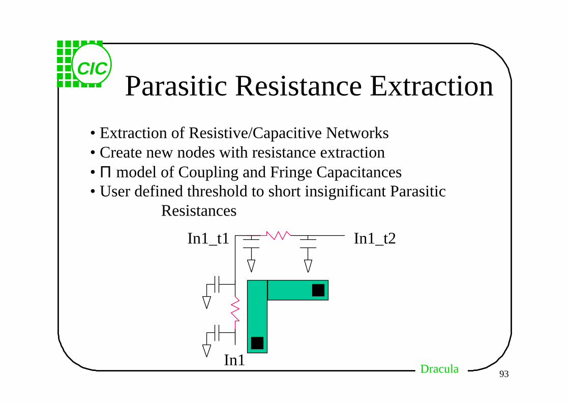
Parasitic Resistance Extraction
• Extraction of Resistive/Capacitive Networks• Create new nodes with resistance extraction• Π model of Coupling and Fringe Capacitances• User defined threshold to short insignificant Parasitic
Resistances
In1
In1_t1 In1_t2
DraculaDracula
CIC
94
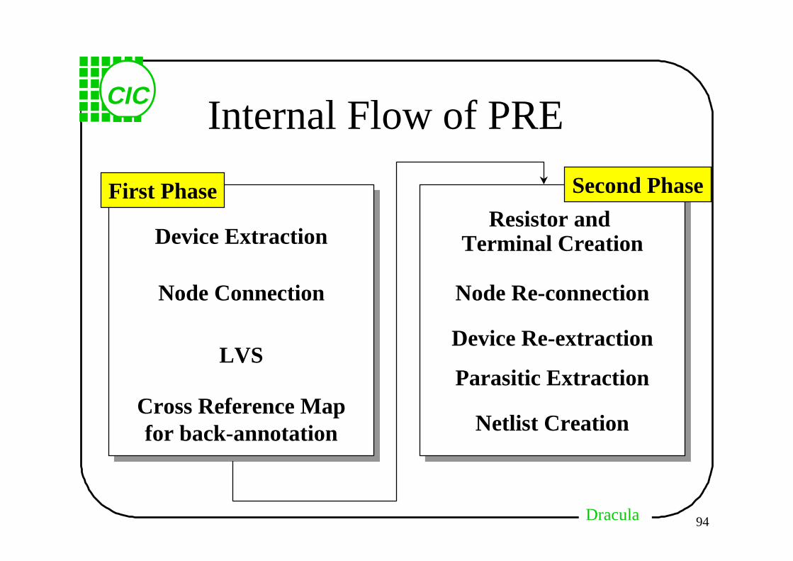
Internal Flow of PRE
Device Extraction
Node Connection
LVS
Cross Reference Mapfor back-annotation
Resistor and Terminal Creation
Node Re-connection
Device Re-extraction
Parasitic Extraction
Netlist Creation
First Phase Second Phase
DraculaDracula
CIC
95
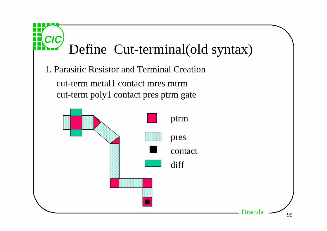
Define Cut-terminal(old syntax)1. Parasitic Resistor and Terminal Creation
cut-term metal1 contact mres mtrmcut-term poly1 contact pres ptrm gate
ptrm
pres
contact
diff
DraculaDracula
CIC
96
Commands for 2nd phase PRE
2. Pad Layer Terminal Creation - defined in input layer
pad-layer = pass
3. Redefine Connectivity with new Terminal Layers
rconnect-layer pwell psd nsd ptrm mtrm
rconnect metal1 mtrm by contactstamp mtrm by metal1
define in the input layer section
DraculaDracula
CIC
97
Commands for 2nd phase PRE4. Extract Designed Devices and Parasitic Devices
5. Generate Netlist
lpeselect[s] mos &lpeselect[s] res gt 0.1 output circuit1
element mos[n] ngate ptrm nsd pwellparasitic res[m] mres mtrmattribute res[m] 0.05
DraculaDracula
CIC
98
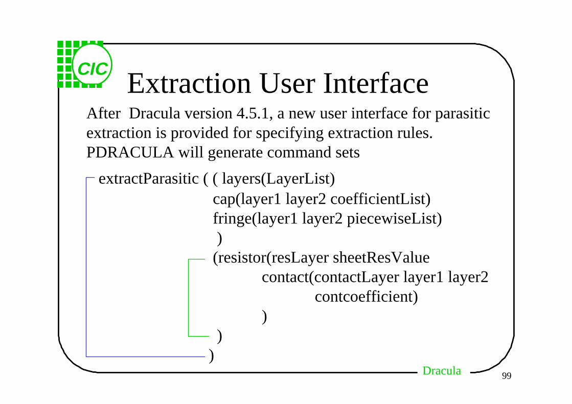
New Extraction User Interface
• New extraction interface is available after Dracula version4.5.1, which is in Cadence after 97a
• Device Reduction option(ConcICe) is also available afterDracula version 4.5.1
• Selective Net Parasitic Extraction
- 2D3B Plate Capacitance- CO/SU/SD Sidewall Capacitance- Piece-Wise Fringe Capacitance
DraculaDracula
CIC
99
Extraction User InterfaceAfter Dracula version 4.5.1, a new user interface for parasiticextraction is provided for specifying extraction rules.PDRACULA will generate command sets
extractParasitic ( ( layers(LayerList) cap(layer1 layer2 coefficientList) fringe(layer1 layer2 piecewiseList) ) (resistor(resLayer sheetResValue contact(contactLayer layer1 layer2 contcoefficient) ) ))
DraculaDracula
CIC
100
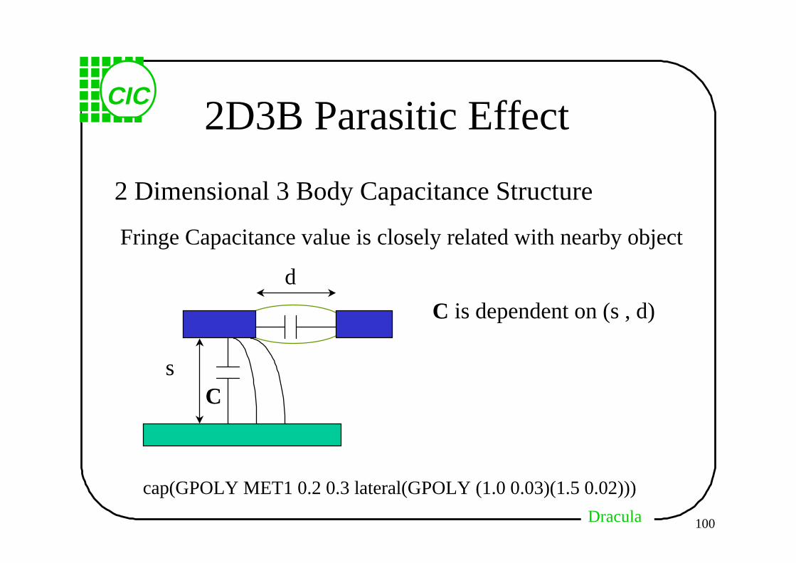
2D3B Parasitic Effect
d
s
2 Dimensional 3 Body Capacitance Structure
Fringe Capacitance value is closely related with nearby object
C
C is dependent on (s , d)
cap(GPOLY MET1 0.2 0.3 lateral(GPOLY (1.0 0.03)(1.5 0.02)))
DraculaDracula
CIC
101
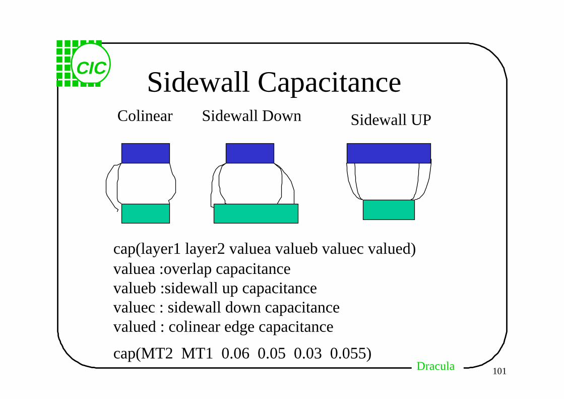
Sidewall CapacitanceColinear Sidewall Down Sidewall UP
cap(MT2 MT1 0.06 0.05 0.03 0.055)
cap(layer1 layer2 valuea valueb valuec valued)valuea :overlap capacitancevalueb :sidewall up capacitancevaluec : sidewall down capacitancevalued : colinear edge capacitance
DraculaDracula
CIC
102
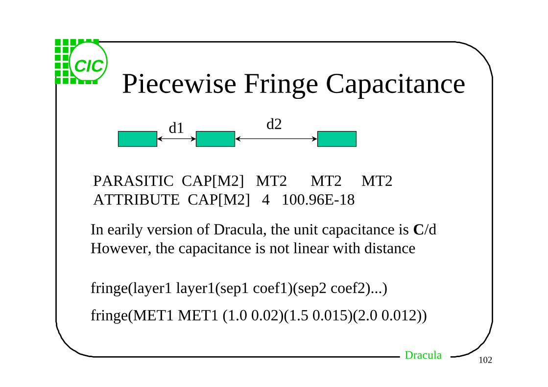
Piecewise Fringe Capacitance
d1 d2
In earily version of Dracula, the unit capacitance is C/dHowever, the capacitance is not linear with distance
PARASITIC CAP[M2] MT2 MT2 MT2ATTRIBUTE CAP[M2] 4 100.96E-18
fringe(layer1 layer1(sep1 coef1)(sep2 coef2)...)
fringe(MET1 MET1 (1.0 0.02)(1.5 0.015)(2.0 0.012))
DraculaDracula
CIC
103
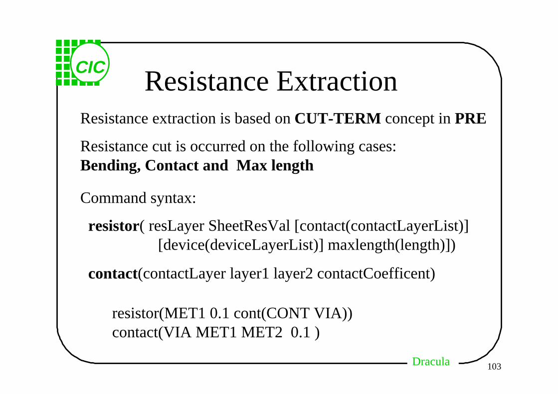
Resistance ExtractionResistance extraction is based on CUT-TERM concept in PRE
Resistance cut is occurred on the following cases: Bending, Contact and Max length
Command syntax:
resistor( resLayer SheetResVal [contact(contactLayerList)][device(deviceLayerList)] maxlength(length)])
contact(contactLayer layer1 layer2 contactCoefficent)
resistor(MET1 0.1 cont(CONT VIA))contact(VIA MET1 MET2 0.1 )
DraculaDracula
CIC
104
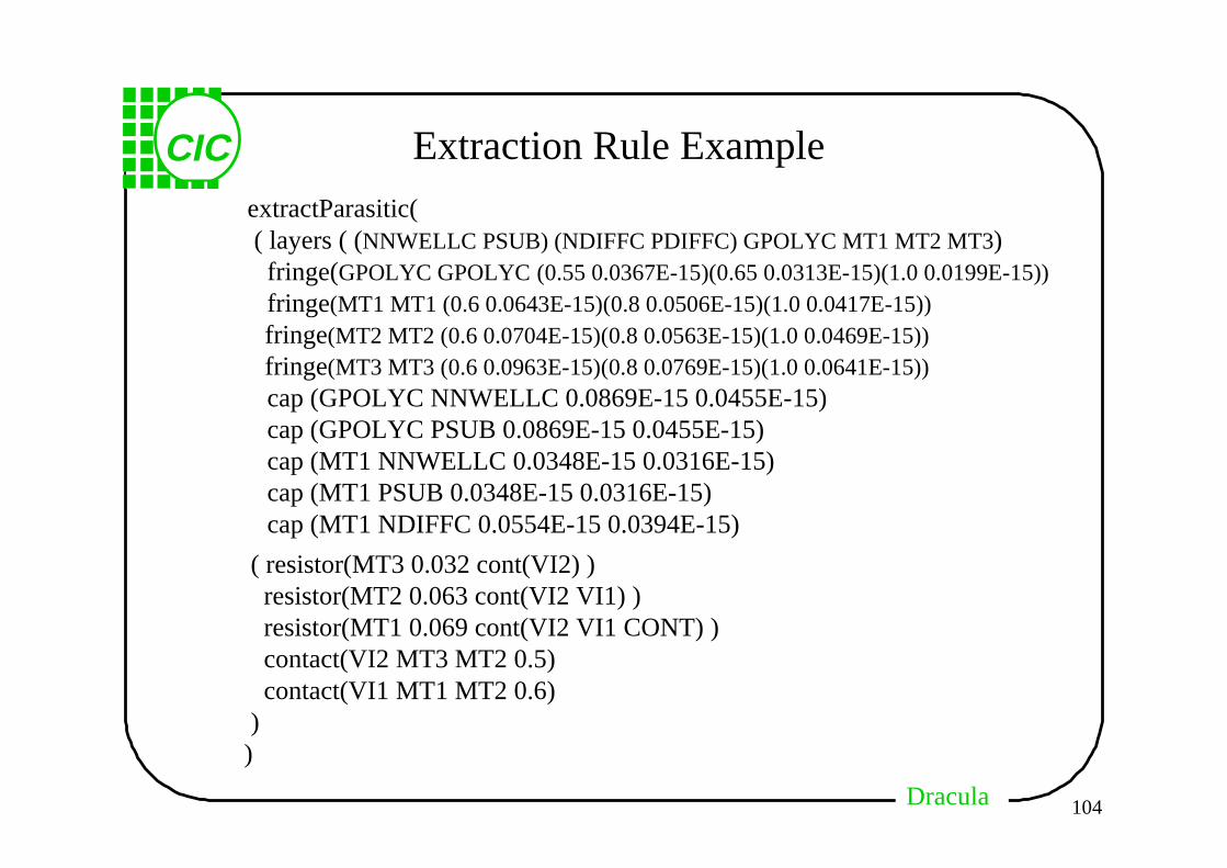
extractParasitic( ( layers ( (NNWELLC PSUB) (NDIFFC PDIFFC) GPOLYC MT1 MT2 MT3) fringe(GPOLYC GPOLYC (0.55 0.0367E-15)(0.65 0.0313E-15)(1.0 0.0199E-15)) fringe(MT1 MT1 (0.6 0.0643E-15)(0.8 0.0506E-15)(1.0 0.0417E-15)) fringe(MT2 MT2 (0.6 0.0704E-15)(0.8 0.0563E-15)(1.0 0.0469E-15)) fringe(MT3 MT3 (0.6 0.0963E-15)(0.8 0.0769E-15)(1.0 0.0641E-15)) cap (GPOLYC NNWELLC 0.0869E-15 0.0455E-15) cap (GPOLYC PSUB 0.0869E-15 0.0455E-15) cap (MT1 NNWELLC 0.0348E-15 0.0316E-15) cap (MT1 PSUB 0.0348E-15 0.0316E-15) cap (MT1 NDIFFC 0.0554E-15 0.0394E-15)
Extraction Rule Example
( resistor(MT3 0.032 cont(VI2) ) resistor(MT2 0.063 cont(VI2 VI1) ) resistor(MT1 0.069 cont(VI2 VI1 CONT) ) contact(VI2 MT3 MT2 0.5) contact(VI1 MT1 MT2 0.6) ))
DraculaDracula
CIC
105
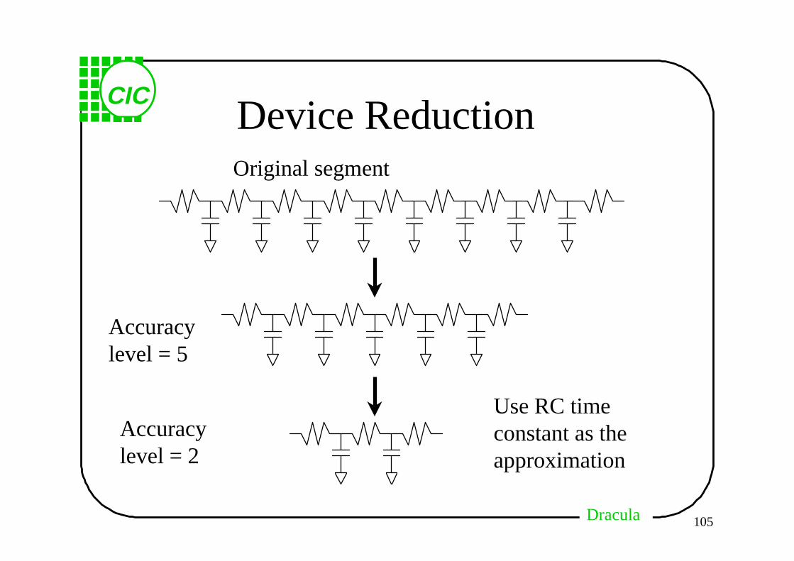
Device Reduction
Accuracylevel = 5
Accuracylevel = 2
Original segment
Use RC timeconstant as theapproximation
DraculaDracula
CIC
106
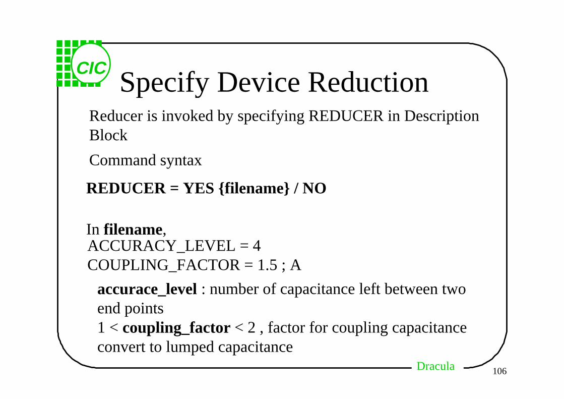
Specify Device ReductionReducer is invoked by specifying REDUCER in DescriptionBlock
Command syntax
REDUCER = YES {filename} / NO
In filename, ACCURACY_LEVEL = 4COUPLING_FACTOR = 1.5 ; A
accurace_level : number of capacitance left between twoend points1 < coupling_factor < 2 , factor for coupling capacitanceconvert to lumped capacitance
DraculaDracula
CIC
107
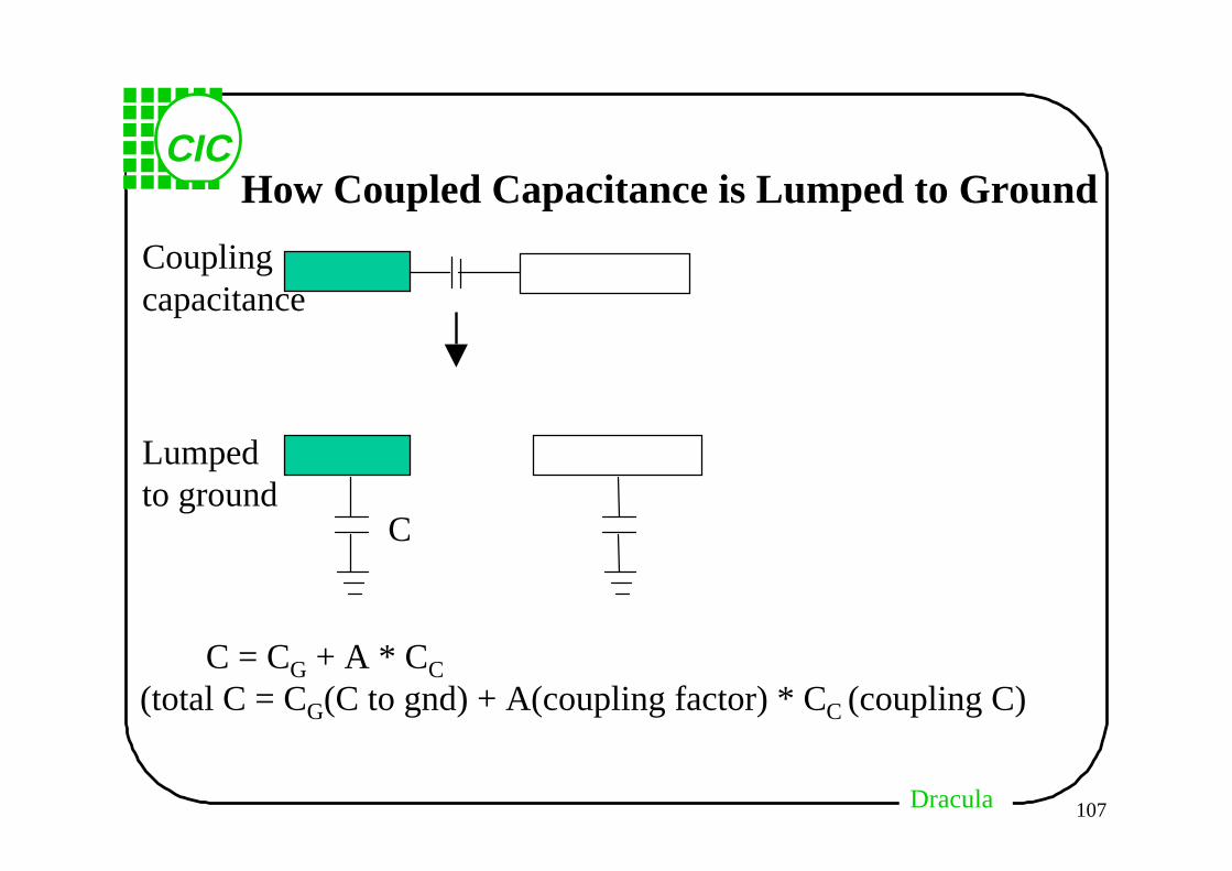
How Coupled Capacitance is Lumped to Ground
Couplingcapacitance
Lumped to ground
C
C = CG + A * CC (total C = CG(C to gnd) + A(coupling factor) * CC (coupling C)
DraculaDracula
CIC
108
Selective LPE• Full chip LPE may generate a large netlist that
make simulation take too much time
• For most circuit, only critical nets are interestedfor timing verification, such as clock, global wires
• Selective LPE will be useful for large circuit thatis timing critical on some nets or paths.
• Simulation time can be reduced as the number ofparasitics reduced
DraculaDracula
CIC
109
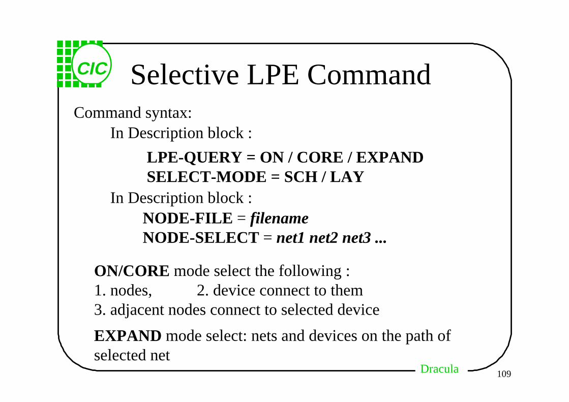
Selective LPE CommandCommand syntax:
In Description block :
In Description block :
LPE-QUERY = ON / CORE / EXPANDSELECT-MODE = SCH / LAY
NODE-FILE = filenameNODE-SELECT = net1 net2 net3 ...
ON/CORE mode select the following :1. nodes, 2. device connect to them3. adjacent nodes connect to selected device
EXPAND mode select: nets and devices on the path ofselected net
DraculaDracula
CIC
110
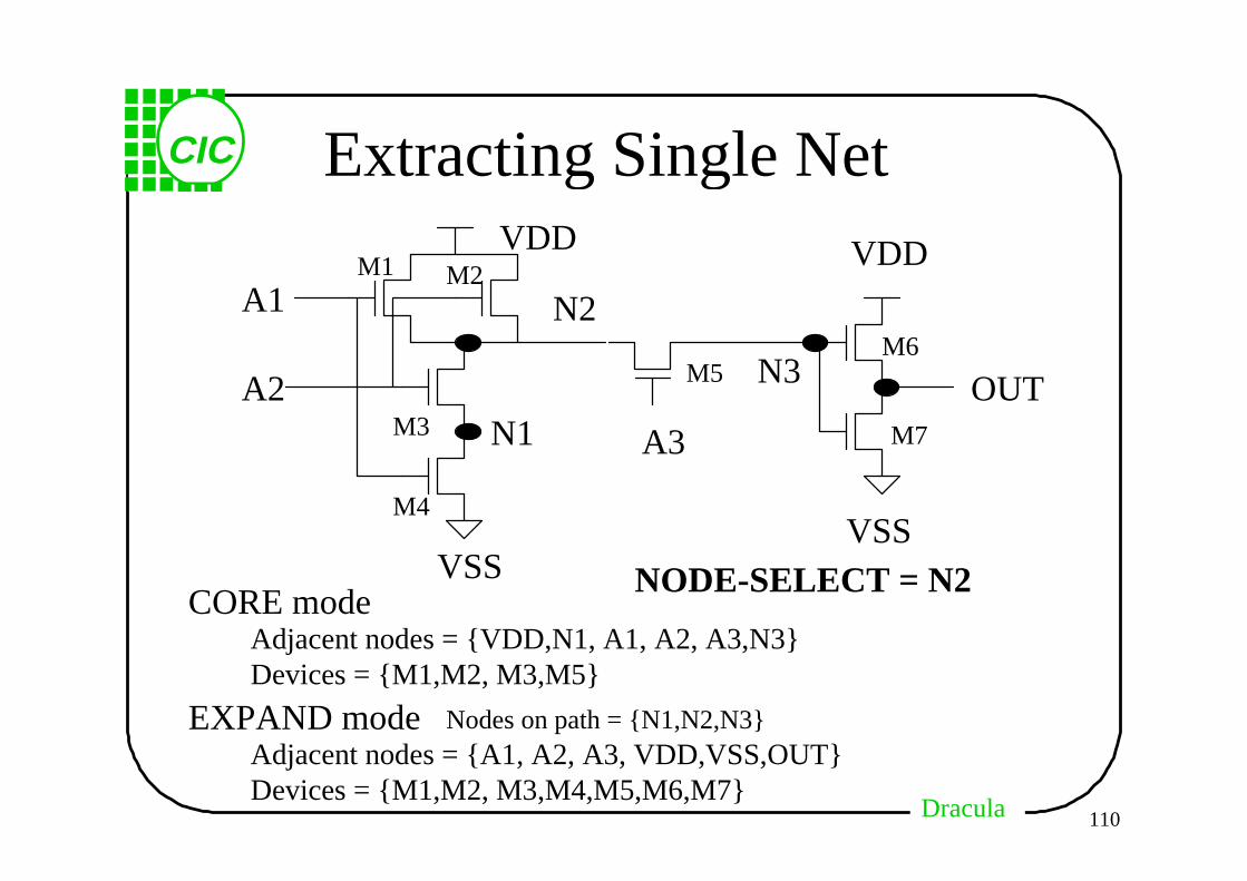
Extracting Single Net
N2A1
VDD VDD
VSSVSS
N1A2
A3
M1 M2
M3
M4
M5M6
M7
CORE modeNODE-SELECT = N2
Adjacent nodes = {VDD,N1, A1, A2, A3,N3}Devices = {M1,M2, M3,M5}
N3
EXPAND modeAdjacent nodes = {A1, A2, A3, VDD,VSS,OUT}Devices = {M1,M2, M3,M4,M5,M6,M7}
OUT
Nodes on path = {N1,N2,N3}