Embed Size (px)
Citation preview
Available online at www.sciencedirect.com
Physics Procedia 00 (2008) 000–000
www.elsevier.com/locate/XXX
Proceedings of the JMSM 2008 Conference
Investigation of the electro-optical behaviour of UV-curedpolymer/liquid crystal systems
F. Z. Abdounea, L. Benkhaledb, L. Méchernènea, U. Maschkeb*a Laboratoire de Recherche sur les Macromolécules, Faculté des Sciences, Université Aboubakr Belkaïd, BP 119,
13000 Tlemcen, Algérieb Laboratoire de Chimie Macromoléculaire (UMR CNRS N° 8009), Bâtiment C6, Université des Sciences et
Technologies de Lille, F-59655 Villeneuve d’Ascq Cedex, France
Elsevier use only: Received date here; revised date here; accepted date here
Abstract
The electro-optical proprieties of Polymer Dispersed Liquid Crystal (PDLC) films were studied to understand the relationshipbetween the conditions of preparation, the morphology, and the response to an external electrical field. The PDLC films wereobtained by polymerization induced phase separation (PIPS) process using Ultra-violet (UV) cured system composed of amonomeric diacrylate and a nematic liquid crystal using two irradiation doses, 50mJ/cm2 and 150mJ/cm2. The analysis of electro-optical responses were investigated in terms of transmission vs voltage curves as a function of thickness and show similar shapes,low transmission in the off-state and high transmission in the on-state in both cases. The results obtained for 150mJ/cm2 exhibitslightly lower switching voltages and in particular, the 50mJ/cm2 samples lead to relatively large dispersed data in terms ofthreshold voltages.© 2009 Elsevier B.V. All rights reserved
PACS: Type pacs here, separated by semicolons ;
Keywords: Polymer, liquid crystal; polymer dispersed liquid crystal; ultraviolet curing
1. INTRODUCTION
The applications of Polymer Dispersed Liquid Crystal (PDLC) materials are generally based on electro-opticalresponse functions, such as optical shutters, large area displays and smart windows [1-5]. PDLC films consist ofmicron-sized nematic liquid crystalline (LC) domains dispersed in a polymer matrix. Since the LC molecules canchange their orientation under the influence of an applied electrical field, the PDLC film switch under certainconditions between an opaque light scattering off-state to a transparent on-state. In this work, PDLC films wereprepared by ultraviolet (UV) irradiation induced polymerization from a homogeneous mixture oftripropyleneglycoldiacrylate (TPGDA) monomer, nematic LC blend E7, and a photoinitiator. When the
* Corresponding author. Tel.: 0033-3-20-33-63-81; fax: +0033-3-20-43-43-45.E-mail address: [email protected].
Received 1 January 2009; received in revised form 31 July 2009; accepted 31 August 2009
Physics Procedia 2 (2009) 643–648
www.elsevier.com/locate/procedia
doi:10.1016/j.phpro.2009.11.005
2 F. Z. Abdoune et al/ Physics Procedia 00 (2009) 000–000
polymerization/cross-linking reactions occur, the LC phase separates from the growing polymer network, formingdomains dispersed in the polymer matrix.
The electro-optical performance of PDLC films such as threshold and switching voltages, off-state and on-statetransmissions, response times, brightness, and contrast are strongly affected by the conditions of preparation leadingto different morphologies in terms of size and shape of the LC domains, and in particular the architecture of thepolymer network [6-12].
The authors report on the dependence of the UV-curing conditions on morphology and electro-optical propertiesby varying both the UV lamp power and the curing time [13–14]. However, the control of the extent of thepolymerization/crosslinking reactions is of prime importance for good and reproducible electro-optical performance.It is, therefore, important to achieve complete conversion of the monomer to the polymer network independent ofthe particular choice of UV light intensities and exposure times. In this paper, the electro-optical response in termsof the transmission as function of applied voltage and film thickness was obtained for the two chosen UV-curingdoses (50mJ/cm2 and 150 mJ/cm2). These results are discussed and compared to observations of the morphologyobtained by Scanning Electron Microscopy (SEM) measurements.
2. EXPERIMENTAL SECTION
2.1. Materials
Tripropyleneglycoldiacrylate (TPGDA) (UCB, Belgium) was used as monomer. The nematic LC E7, an eutecticmixture containing four cyanoparaphenylene derivatives, was employed in this work exhibiting a positive dielectricanisotropy and a nematic-isotropic transition temperature at TNI =61°C. 30 weight-percent (wt-%) of TPGDA, 70wt-% of E7, and 2wt-% (of the acrylate mixture) of a photoinitiator (Lucirin TPO, BASF) were mixed together until theblend became homogeneous.
2.1.Sample Preparation
For electro-optical investigations, the initial reactive mixture was sandwiched between a glass plate and a 100 μmthick Polyethyleneterephthalate (PET) sheet (Renker, Germany), both coated with a thin transparent layer ofconducting indium/tin oxide. The film thickness was measured by an adapted micrometer calliper (Mitutoyo;diameter 1mm; uncertainty: ±1 μm). The precise place of crossing of the laser beam through the film, exhibiting adiameter of about one millimeter, is considered to take repetitive measurements (at least five times) of the thicknessof the PDLC sample. Then, measurements of the thicknesses are taken separately on the two supports, namelyglass/ITO and PET/ITO, which were cleaned before, once the sandwich (glass-ITO/PDLC film/PET-ITO) wasopened. The irregularities of the thickness of the samples were thus taken into account since the measurements werecarried out exactly on the crossing point of the laser beam.
2.2. Instrumentation
The UV irradiation source used in this study was a Minicure Model MC4-300 (Primarc UV Technology)equipped with a medium pressure mercury arc lamp rated 80 W/cm. The samples prepared as described above wereplaced on a conveyor belt; the dose received by the sample was either 50 mJ/cm2 or 150 mJ/cm2.
The electro-optical measurements were carried out by a standard set-up including a laser, a sample holder and aphotodiode together with a computer controlled data acquisition for the analysis of the electro-optical properties.The transmission of unpolarized HeNe laser light (�= 632.8 nm) passing perpendicular through the PDLC film wasmeasured at room temperature without and upon application of an external electrical field. Several sinusoidalvoltage scan up and down cycles with appropriate maximum voltages were applied during a period of 120 s, using afrequency of 145 Hz.
Samples for Scanning Electron Microscope (SEM) studies were elaborated in the same way as described abovefor electro-optical measurements. After irradiation exposure was finished, the sample cells were opened andimmersed in tetrahydrofuran in order to extract the LC. The samples were then coated by a thin platinum layer and
644 F.Z. Abdoune et al. / Physics Procedia 2 (2009) 643–648
F. Z. Abdoune et al/ Physics Procedia 00 (2009) 000–000 3
characterized by a SEM (Philips XL-30 field emission gun). This sample preparation technique leads to theappearance of dark holes that were once filled with LC. The magnification used in our experiments was about20000x using an acceleration voltage of 10kV.
3. RESULTS AND DISCUSSION
Important physical properties of PDLC films such as the electro-optical response and the mechanical behavior aredirectly related with the conditions under which the materials are obtained. In particular, the kinetics ofphotopolymerization and the phase separation behavior of the monomer/LC blend govern the architecture of theobtained polymer network. In order to analyse the extent of formation of the polymer network, the relationshipbetween the conversion of the monomer and the curing conditions was investigated. It is evident that high monomerconversions should be reached to minimize undesired effects of unreacted monomers or dangling chains. FTIRspectroscopy was applied as a versatile method to investigate the extent of curing via carbon-carbon double bondconversion. A difunctional acrylic monomer was used in this work giving rise to a chemically crosslinked polymernetwork. The results obtained from FTIR measurements indicate a complete monomer conversion for samples curedwith 50mJ/cm2 and 150mJ/cm2, by considering the peak height of the absorption band at 1637cm-1.
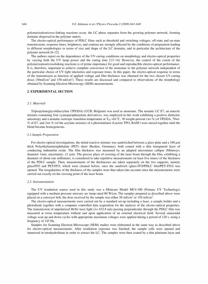
Fig. 1. Electro-optical response of 25 μm thick PDLC films a) 50mJ/cm2, b) 150mJ/cm2. The inset exhibit thecorresponding sample morphology obtained by SEM.
0
10
20
30
40
50
60
70
80
90
100
0 50 100 150 200 250 300 350
Applied Voltage (volts)
Tra
nsm
itta
nce
(%)
Fig. a
0
10
20
30
40
50
60
70
80
90
100
0 50 100 150 200 250 300 350
Applied Voltage (volts)
Tra
nsm
itta
nce
(%)
Fig. a
0
10
20
30
40
50
60
70
80
90
100
0 50 100 150 200 250 300 350
Applied Voltage (Volts)
Tra
nsm
issi
on
(%)
Fig. b
0
10
20
30
40
50
60
70
80
90
100
0 50 100 150 200 250 300 350
Applied Voltage (Volts)
Tra
nsm
issi
on
(%)
0
10
20
30
40
50
60
70
80
90
100
0 50 100 150 200 250 300 350
Applied Voltage (Volts)
Tra
nsm
issi
on
(%)
Fig. b
F.Z. Abdoune et al. / Physics Procedia 2 (2009) 643–648 645
4 F. Z. Abdoune et al/ Physics Procedia 00 (2009) 000–000
Figures 1a and 1b exhibit transmission vs. voltage curves of 25μm thick PDLC films cured with 50mJ/cm2 and150mJ/cm2, respectively. Both electro-optical response curves show low transmission values in the off-state, hightransmission in the on-state, and similar shapes characterized by a slow increase of the transmission uponapplication of an electrical field. Furthermore, the samples show a relatively large hysteresis i.e. in an increasingfield, the transmission at a specific voltage is lower than the transmission at the same voltage in a decreasingelectrical field. The electrical field necessary to switch the 50mJ/cm2 film from an opaque to a transparent state isslightly higher than for the 150mJ/cm2 sample as can be seen by comparing the electro-optical response curvesshown in Figures 1a and 1b.
0
50
100
150
200
250
0 5 10 15 20 25 30 35
Filmthickness (μm)
V10
(Vo
lts)
Fig. a
0
50
100
150
200
250
0 5 10 15 20 25 30 35
Filmthickness (μm)
V10
(Vo
lts)
Fig, b
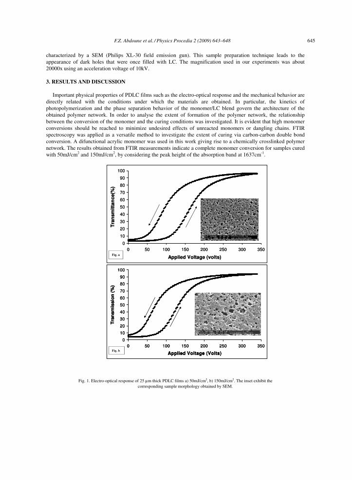
Fig 2. Threshold (V10) voltages as a function of film thickness for UV-cured samples, a) 50 mJ/cm2, b) 150 mJ/cm2.
The electro-optical properties can be explained by the analysis of the corresponding sample morphologies whichare displayed as insets in these figures. Large size distributions of irregularly shaped domains were observed in bothcases and are in good agreement with the slow response to the applied electrical field: LC molecules in largerdomains orient already at low electrical fields whereas LC molecules in smaller domains need higher voltages to
646 F.Z. Abdoune et al. / Physics Procedia 2 (2009) 643–648
F. Z. Abdoune et al/ Physics Procedia 00 (2009) 000–000 5
orient due to the higher curvature of these domains. The morphology analysis reveals increased domain sizes of the150 mJ/cm2 sample compared to 50 mJ/cm2 which lead to the observed shift of the transmission vs. voltage curve tolower values.
Figure 2 shows the threshold voltages as a function of film thickness for a) 50 mJ/cm2 and b) 150 mJ/cm2
samples. Widely dispersed results were found in the case of the lower UV-dose and the experimental data cannot bedescribed by a linear relationship. However, the results can be fitted by a combination of two linear regressioncurves with a change of the slope around a film thickness of 14 μm. On the other hand, the results obtained for the150 mJ/cm2 sample can be described by a single linear fit. Also the performance of these films in terms of electro-optical responses is to achieve a high contrast ratio Ton/Toff. The intensity of transmitted light at right angle wasrecorded as a function of time starting at the time where the applied electric field is removed; and data are taken atroom temperature for two doses.
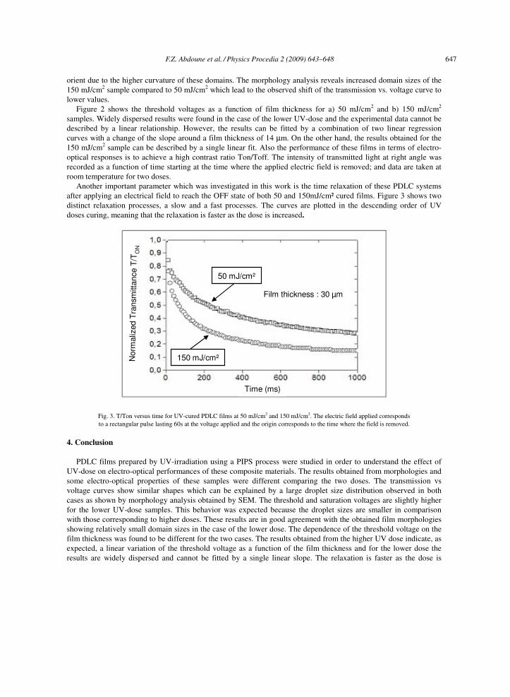
Another important parameter which was investigated in this work is the time relaxation of these PDLC systemsafter applying an electrical field to reach the OFF state of both 50 and 150mJ/cm² cured films. Figure 3 shows twodistinct relaxation processes, a slow and a fast processes. The curves are plotted in the descending order of UVdoses curing, meaning that the relaxation is faster as the dose is increased.
No r
mal
ized
Tr a
n sm
it ta n
c eT
/ TO
N
50 mJ/cm²
150 mJ/cm²
Film thickness : 30 μm
Time (ms)
Nor
mal
ized
Tr a
n sm
it ta n
c eT
/ TO
NN
o rm
aliz
edT
r an s
mit t
a nc e
T/ T
ON
50 mJ/cm²
150 mJ/cm²
Film thickness : 30 μm
Time (ms)
Fig. 3. T/Ton versus time for UV-cured PDLC films at 50 mJ/cm2 and 150 mJ/cm2. The electric field applied correspondsto a rectangular pulse lasting 60s at the voltage applied and the origin corresponds to the time where the field is removed.
4. Conclusion
PDLC films prepared by UV-irradiation using a PIPS process were studied in order to understand the effect ofUV-dose on electro-optical performances of these composite materials. The results obtained from morphologies andsome electro-optical properties of these samples were different comparing the two doses. The transmission vsvoltage curves show similar shapes which can be explained by a large droplet size distribution observed in bothcases as shown by morphology analysis obtained by SEM. The threshold and saturation voltages are slightly higherfor the lower UV-dose samples. This behavior was expected because the droplet sizes are smaller in comparisonwith those corresponding to higher doses. These results are in good agreement with the obtained film morphologiesshowing relatively small domain sizes in the case of the lower dose. The dependence of the threshold voltage on thefilm thickness was found to be different for the two cases. The results obtained from the higher UV dose indicate, asexpected, a linear variation of the threshold voltage as a function of the film thickness and for the lower dose theresults are widely dispersed and cannot be fitted by a single linear slope. The relaxation is faster as the dose is
F.Z. Abdoune et al. / Physics Procedia 2 (2009) 643–648 647

6 F. Z. Abdoune et al/ Physics Procedia 00 (2009) 000–000
150mJ/cm2, a possible explanation of this phenomenon could be probably the morphology of these films as seenabove and the architecture of the polymer network that can be formed differently for the two irradiation doses.
References
[1] J. W. Doane, N. A. Vaz, B. G. Wu, S. Zumer, Appl. Phys. Lett. 48 (1986) 269[2] J. W. Doane, G Chidichimo, N. A. Vaz, US Patent, 4, 688 (1987) 900[3] U. Maschke, X. Coqueret, M. Benmouna, Macromol. Rapid Comm. 23 (2002)159.[4] M. Mucha, Prog. Polym. Sci. 28 (2003) 837.[5] C. M. Lampert, Chromogenic Smart Materiels, Materials Today, 2004.[6] G. W. Smith, N.A. Vaz, Liq. Cryst. 3 (1988) 543.[7] V.G. Nazarenko, S. Sarala. N.V. Madhusudana, Jpn. J. Appl. Phys. 33 (1994) 2641.[8] A.J. Lovinger, K.R. Amundson, D.D. Davis, Chem. Mat. 6 (1994) 1726.[9] J.D. LeGrange, S.A. Carter, M. Fuentes, J. Boo, A.E. Freeny, W. Cleveland, T.M. Miller, J. Appl. Phys. 81 (1997) 5984.[10] C. Grand, M.F. Achard, F. Hardouin, Liq. Cryst., 22 (1997) 287.[11] W. Li, Y. Cao, H. Cao, M. Kashima, L. Kong, H. Yang, J. Polym. Sci.: Part B: Polym. Phys. 46 (2008) 1369.[12] T.J. White, L.V. Natarajan, T.J. Bunning, C.A. Guymon, Liq. Cryst. 34 (2007) 1377.[13] A.M. Lackner, J.D. Margerum, E. Ramos, K.-C. Lim, SPIE. 1080 (1989) 53.[14] E. Nastal, E. Zuranska, M. Mucha, J. Appl. Polym. Sci. 71 (1999) 445.
648 F.Z. Abdoune et al. / Physics Procedia 2 (2009) 643–648