Embed Size (px)
Citation preview
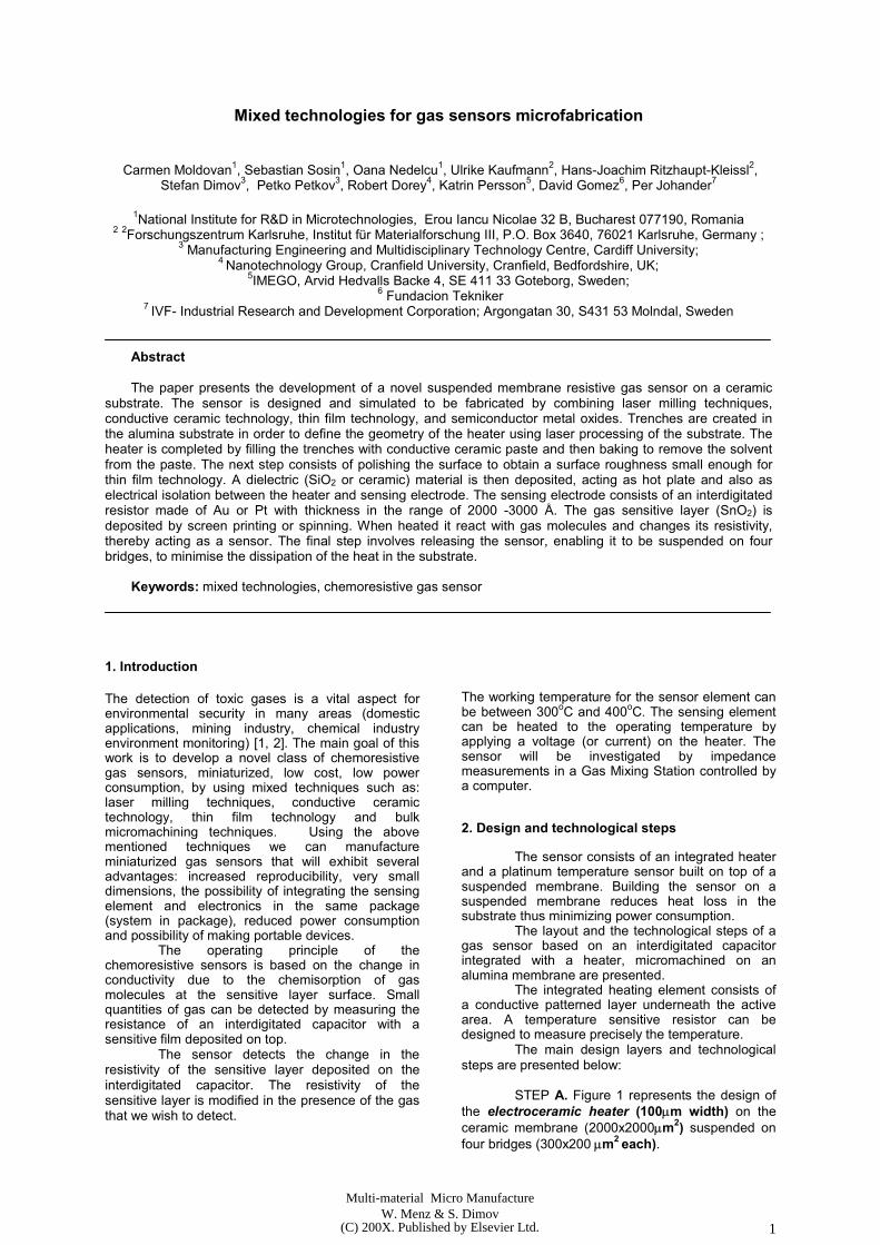
Mixed technologies for gas sensors microfabrication
Carmen Moldovan1, Sebastian Sosin1, Oana Nedelcu1, Ulrike Kaufmann2, Hans-Joachim Ritzhaupt-Kleissl2, Stefan Dimov3, Petko Petkov3, Robert Dorey4, Katrin Persson5, David Gomez6, Per Johander7
1National Institute for R&D in Microtechnologies, Erou Iancu Nicolae 32 B, Bucharest 077190, Romania
2 2Forschungszentrum Karlsruhe, Institut für Materialforschung III, P.O. Box 3640, 76021 Karlsruhe, Germany ; 3 Manufacturing Engineering and Multidisciplinary Technology Centre, Cardiff University;
4 Nanotechnology Group, Cranfield University, Cranfield, Bedfordshire, UK; 5IMEGO, Arvid Hedvalls Backe 4, SE 411 33 Goteborg, Sweden;
6 Fundacion Tekniker 7 IVF- Industrial Research and Development Corporation; Argongatan 30, S431 53 Molndal, Sweden
Abstract The paper presents the development of a novel suspended membrane resistive gas sensor on a ceramic
substrate. The sensor is designed and simulated to be fabricated by combining laser milling techniques, conductive ceramic technology, thin film technology, and semiconductor metal oxides. Trenches are created in the alumina substrate in order to define the geometry of the heater using laser processing of the substrate. The heater is completed by filling the trenches with conductive ceramic paste and then baking to remove the solvent from the paste. The next step consists of polishing the surface to obtain a surface roughness small enough for thin film technology. A dielectric (SiO2 or ceramic) material is then deposited, acting as hot plate and also as electrical isolation between the heater and sensing electrode. The sensing electrode consists of an interdigitated resistor made of Au or Pt with thickness in the range of 2000 -3000 Å. The gas sensitive layer (SnO2) is deposited by screen printing or spinning. When heated it react with gas molecules and changes its resistivity, thereby acting as a sensor. The final step involves releasing the sensor, enabling it to be suspended on four bridges, to minimise the dissipation of the heat in the substrate. Keywords: mixed technologies, chemoresistive gas sensor
1. Introduction
The detection of toxic gases is a vital aspect for environmental security in many areas (domestic applications, mining industry, chemical industry environment monitoring) [1, 2]. The main goal of this work is to develop a novel class of chemoresistive gas sensors, miniaturized, low cost, low power consumption, by using mixed techniques such as: laser milling techniques, conductive ceramic technology, thin film technology and bulk micromachining techniques. Using the above mentioned techniques we can manufacture miniaturized gas sensors that will exhibit several advantages: increased reproducibility, very small dimensions, the possibility of integrating the sensing element and electronics in the same package (system in package), reduced power consumption and possibility of making portable devices.
The operating principle of the chemoresistive sensors is based on the change in conductivity due to the chemisorption of gas molecules at the sensitive layer surface. Small quantities of gas can be detected by measuring the resistance of an interdigitated capacitor with a sensitive film deposited on top.
The sensor detects the change in the resistivity of the sensitive layer deposited on the interdigitated capacitor. The resistivity of the sensitive layer is modified in the presence of the gas that we wish to detect.
The working temperature for the sensor element can be between 300oC and 400oC. The sensing element can be heated to the operating temperature by applying a voltage (or current) on the heater. The sensor will be investigated by impedance measurements in a Gas Mixing Station controlled by a computer.
2. Design and technological steps
The sensor consists of an integrated heater and a platinum temperature sensor built on top of a suspended membrane. Building the sensor on a suspended membrane reduces heat loss in the substrate thus minimizing power consumption.
The layout and the technological steps of a gas sensor based on an interdigitated capacitor integrated with a heater, micromachined on an alumina membrane are presented.
The integrated heating element consists of a conductive patterned layer underneath the active area. A temperature sensitive resistor can be designed to measure precisely the temperature.
The main design layers and technological steps are presented below:
STEP A. Figure 1 represents the design of
the electroceramic heater (100µm width) on the ceramic membrane (2000x2000µm2) suspended on four bridges (300x200 µm2 each).
1(C) 200X. Published by Elsevier Ltd.W. Menz & S. Dimov
Multi-material Micro Manufacture
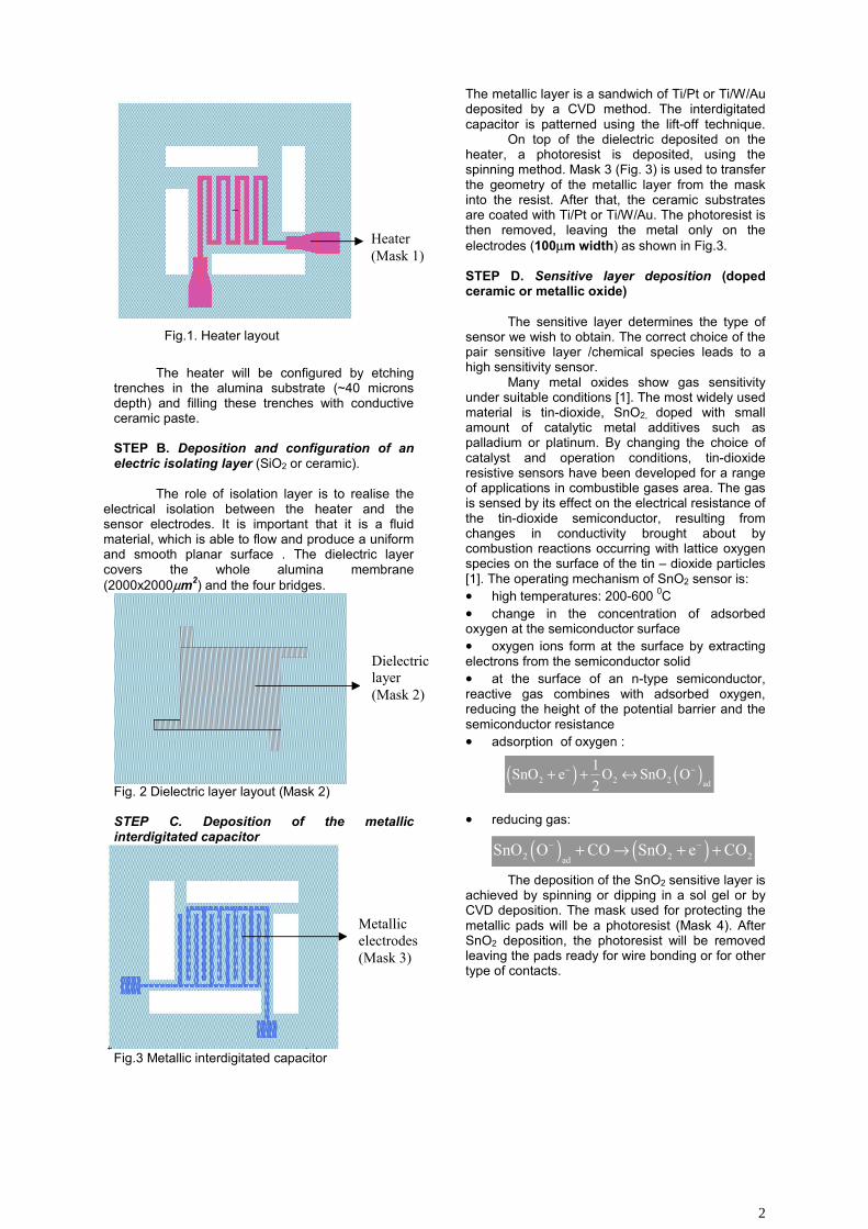
The heater will be configured by etching trenches in the alumina substrate (~40 microns depth) and filling these trenches with conductive ceramic paste. STEP B. Deposition and configuration of an electric isolating layer (SiO2 or ceramic).
The role of isolation layer is to realise the electrical isolation between the heater and the sensor electrodes. It is important that it is a fluid material, which is able to flow and produce a uniform and smooth planar surface . The dielectric layer covers the whole alumina membrane (2000x2000µm2) and the four bridges.
Fig. 2 Dielectric layer layout (Mask 2) STEP C. Deposition of the metallic interdigitated capacitor
Fig.3 Metallic interdigitated capacitor
The metallic layer is a sandwich of Ti/Pt or Ti/W/Au deposited by a CVD method. The interdigitated capacitor is patterned using the lift-off technique. On top of the dielectric deposited on the heater, a photoresist is deposited, using the spinning method. Mask 3 (Fig. 3) is used to transfer the geometry of the metallic layer from the mask into the resist. After that, the ceramic substrates are coated with Ti/Pt or Ti/W/Au. The photoresist is then removed, leaving the metal only on the electrodes (100µm width) as shown in Fig.3. STEP D. Sensitive layer deposition (doped ceramic or metallic oxide) The sensitive layer determines the type of sensor we wish to obtain. The correct choice of the pair sensitive layer /chemical species leads to a high sensitivity sensor. Many metal oxides show gas sensitivity under suitable conditions [1]. The most widely used material is tin-dioxide, SnO2, doped with small amount of catalytic metal additives such as palladium or platinum. By changing the choice of catalyst and operation conditions, tin-dioxide resistive sensors have been developed for a range of applications in combustible gases area. The gas is sensed by its effect on the electrical resistance of the tin-dioxide semiconductor, resulting from changes in conductivity brought about by combustion reactions occurring with lattice oxygen species on the surface of the tin – dioxide particles [1]. The operating mechanism of SnO2 sensor is: • high temperatures: 200-600 0C • change in the concentration of adsorbed oxygen at the semiconductor surface • oxygen ions form at the surface by extracting electrons from the semiconductor solid • at the surface of an n-type semiconductor, reactive gas combines with adsorbed oxygen, reducing the height of the potential barrier and the semiconductor resistance • adsorption of oxygen : • reducing gas:
The deposition of the SnO2 sensitive layer is achieved by spinning or dipping in a sol gel or by CVD deposition. The mask used for protecting the metallic pads will be a photoresist (Mask 4). After SnO2 deposition, the photoresist will be removed leaving the pads ready for wire bonding or for other type of contacts.
Heater (Mask 1)
Fig.1. Heater layout
Dielectric layer (Mask 2)
Metallic electrodes (Mask 3)
( ) ( )2 2 2 ad
1SnO e O SnO O2
− −+ + ↔
( ) ( )2 2 2adSnO O CO SnO e CO− −+ → + +
2
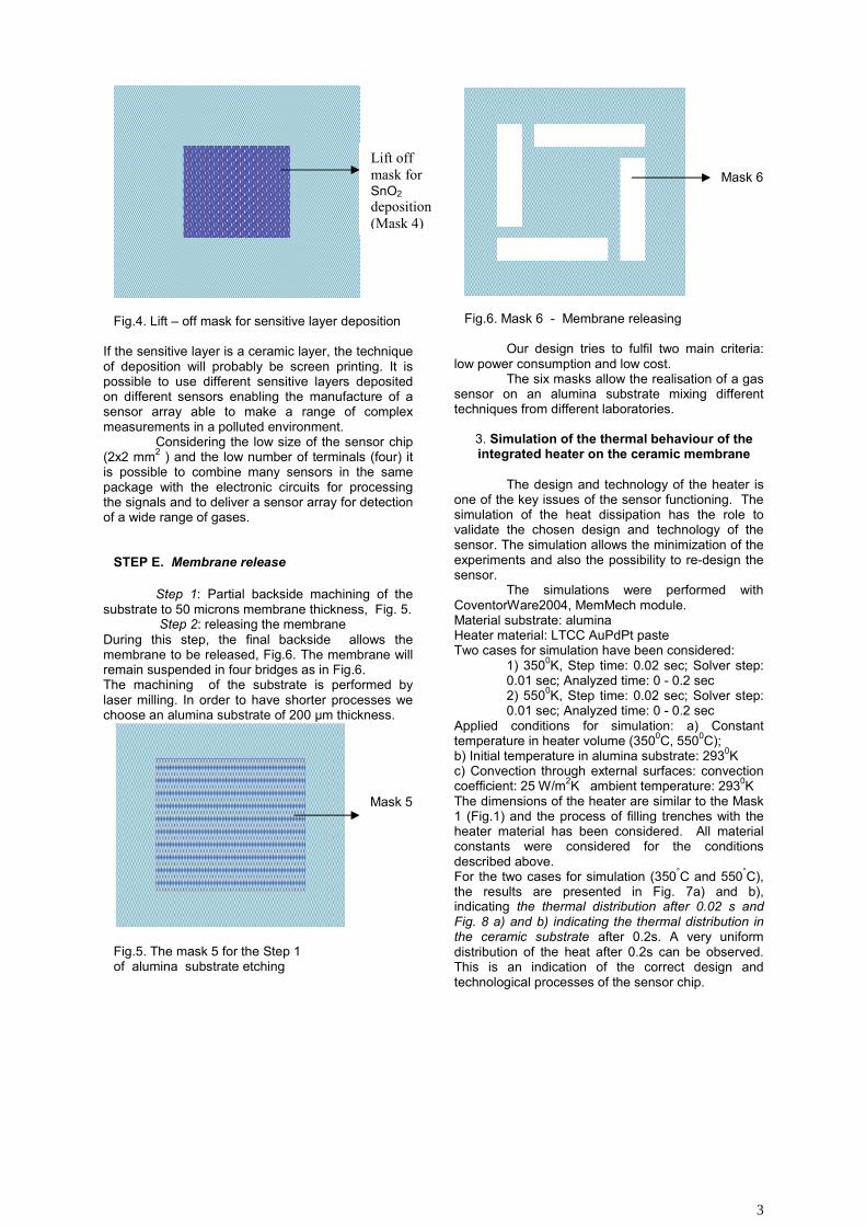
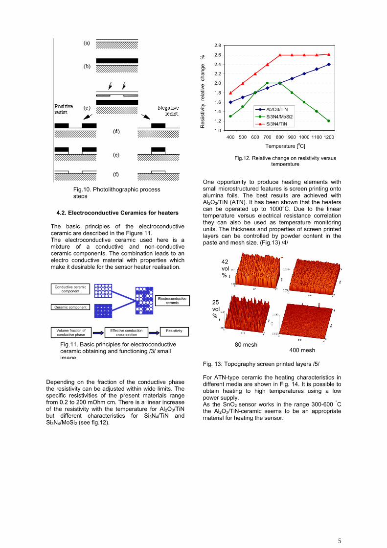
Fig.4. Lift – off mask for sensitive layer deposition
If the sensitive layer is a ceramic layer, the technique of deposition will probably be screen printing. It is possible to use different sensitive layers deposited on different sensors enabling the manufacture of a sensor array able to make a range of complex measurements in a polluted environment. Considering the low size of the sensor chip (2x2 mm2 ) and the low number of terminals (four) it is possible to combine many sensors in the same package with the electronic circuits for processing the signals and to deliver a sensor array for detection of a wide range of gases.
STEP E. Membrane release
Step 1: Partial backside machining of the substrate to 50 microns membrane thickness, Fig. 5.
Step 2: releasing the membrane During this step, the final backside allows the membrane to be released, Fig.6. The membrane will remain suspended in four bridges as in Fig.6. The machining of the substrate is performed by laser milling. In order to have shorter processes we choose an alumina substrate of 200 µm thickness.
Fig.5. The mask 5 for the Step 1 of alumina substrate etching
Fig.6. Mask 6 - Membrane releasing
Our design tries to fulfil two main criteria: low power consumption and low cost. The six masks allow the realisation of a gas sensor on an alumina substrate mixing different techniques from different laboratories.
3. Simulation of the thermal behaviour of the integrated heater on the ceramic membrane
The design and technology of the heater is one of the key issues of the sensor functioning. The simulation of the heat dissipation has the role to validate the chosen design and technology of the sensor. The simulation allows the minimization of the experiments and also the possibility to re-design the sensor. The simulations were performed with CoventorWare2004, MemMech module. Material substrate: alumina Heater material: LTCC AuPdPt paste Two cases for simulation have been considered:
1) 3500K, Step time: 0.02 sec; Solver step: 0.01 sec; Analyzed time: 0 - 0.2 sec 2) 5500K, Step time: 0.02 sec; Solver step: 0.01 sec; Analyzed time: 0 - 0.2 sec
Applied conditions for simulation: a) Constant temperature in heater volume (3500C, 5500C); b) Initial temperature in alumina substrate: 2930K c) Convection through external surfaces: convection coefficient: 25 W/m2K ambient temperature: 2930K The dimensions of the heater are similar to the Mask 1 (Fig.1) and the process of filling trenches with the heater material has been considered. All material constants were considered for the conditions described above. For the two cases for simulation (350°C and 550°C), the results are presented in Fig. 7a) and b), indicating the thermal distribution after 0.02 s and Fig. 8 a) and b) indicating the thermal distribution in the ceramic substrate after 0.2s. A very uniform distribution of the heat after 0.2s can be observed. This is an indication of the correct design and technological processes of the sensor chip.
Mask 5
Mask 6 Lift off mask for SnO2 deposition (Mask 4)
3
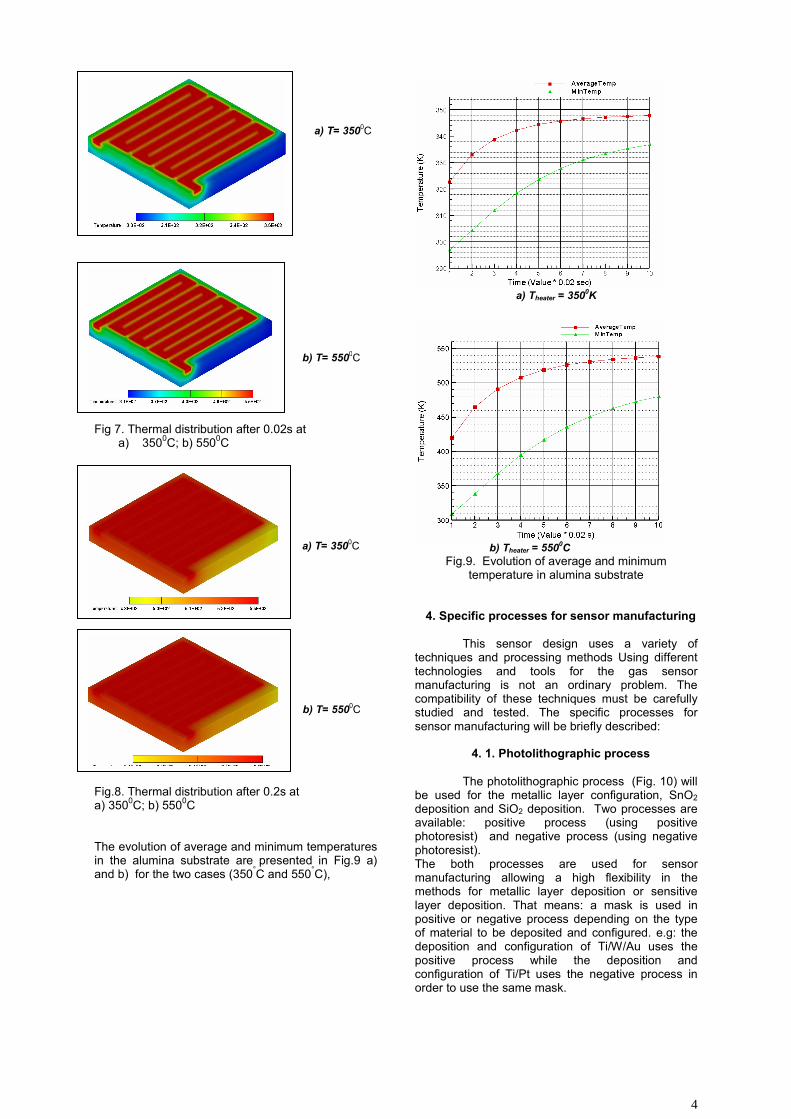
Fig 7. Thermal distribution after 0.02s at a) 3500C; b) 5500C
a) T= 3500C b) T= 5500C
Fig.8. Thermal distribution after 0.2s at a) 3500C; b) 5500C The evolution of average and minimum temperatures in the alumina substrate are presented in Fig.9 a) and b) for the two cases (350°C and 550°C),
a) Theater = 3500K
b) Theater = 5500C
Fig.9. Evolution of average and minimum temperature in alumina substrate
4. Specific processes for sensor manufacturing
This sensor design uses a variety of techniques and processing methods Using different technologies and tools for the gas sensor manufacturing is not an ordinary problem. The compatibility of these techniques must be carefully studied and tested. The specific processes for sensor manufacturing will be briefly described:
4. 1. Photolithographic process
The photolithographic process (Fig. 10) will be used for the metallic layer configuration, SnO2 deposition and SiO2 deposition. Two processes are available: positive process (using positive photoresist) and negative process (using negative photoresist). The both processes are used for sensor manufacturing allowing a high flexibility in the methods for metallic layer deposition or sensitive layer deposition. That means: a mask is used in positive or negative process depending on the type of material to be deposited and configured. e.g: the deposition and configuration of Ti/W/Au uses the positive process while the deposition and configuration of Ti/Pt uses the negative process in order to use the same mask.
a) T= 3500C
b) T= 5500C
4
4.2. Electroconductive Ceramics for heaters
The basic principles of the electroconductive ceramic are described in the Figure 11. The electroconductive ceramic used here is a mixture of a conductive and non-conductive ceramic components. The combination leads to an electro conductive material with properties which make it desirable for the sensor heater realisation.
Depending on the fraction of the conductive phase the resistivity can be adjusted within wide limits. The specific resistivities of the present materials range from 0.2 to 200 mOhm cm. There is a linear increase of the resistivity with the temperature for Al2O3/TiN but different characteristics for Si3N4/TiN and Si3N4/MoSi2 (see fig.12).
One opportunity to produce heating elements with small microstructured features is screen printing onto alumina foils. The best results are achieved with Al2O3/TiN (ATN). It has been shown that the heaters can be operated up to 1000°C. Due to the linear temperature versus electrical resistance correlation they can also be used as temperature monitoring units. The thickness and properties of screen printed layers can be controlled by powder content in the paste and mesh size. (Fig.13) /4/
Fig. 13: Topography screen printed layers /5/ For ATN-type ceramic the heating characteristics in different media are shown in Fig. 14. It is possible to obtain heating to high temperatures using a low power supply. As the SnO2 sensor works in the range 300-600 °C the Al2O3/TiN-ceramic seems to be an appropriate material for heating the sensor.
Electroconductive ceramic
Volume fraction of conductive phase
Effective conduction cross-section
Resistivity
Conductive ceramic component
Ceramic component
Fig.10. Photolithographic process steps
Fig.11. Basic principles for electroconductive ceramic obtaining and functioning /3/ small image
1.0
1.2
1.4
1.6
1.8
2.0
2.2
2.4
2.6
2.8
400 500 600 700 800 900 1000 1100 1200
Al2O3/TiNSi3N4/MoSi2 Si3N4/TiN
Temperature [0C]
Fig.12. Relative change on resistivity versus temperature
Res
iistiv
ity r
elat
ive
cha
nge
%
80 mesh 400 mesh
42 vol%
25 vol%
5
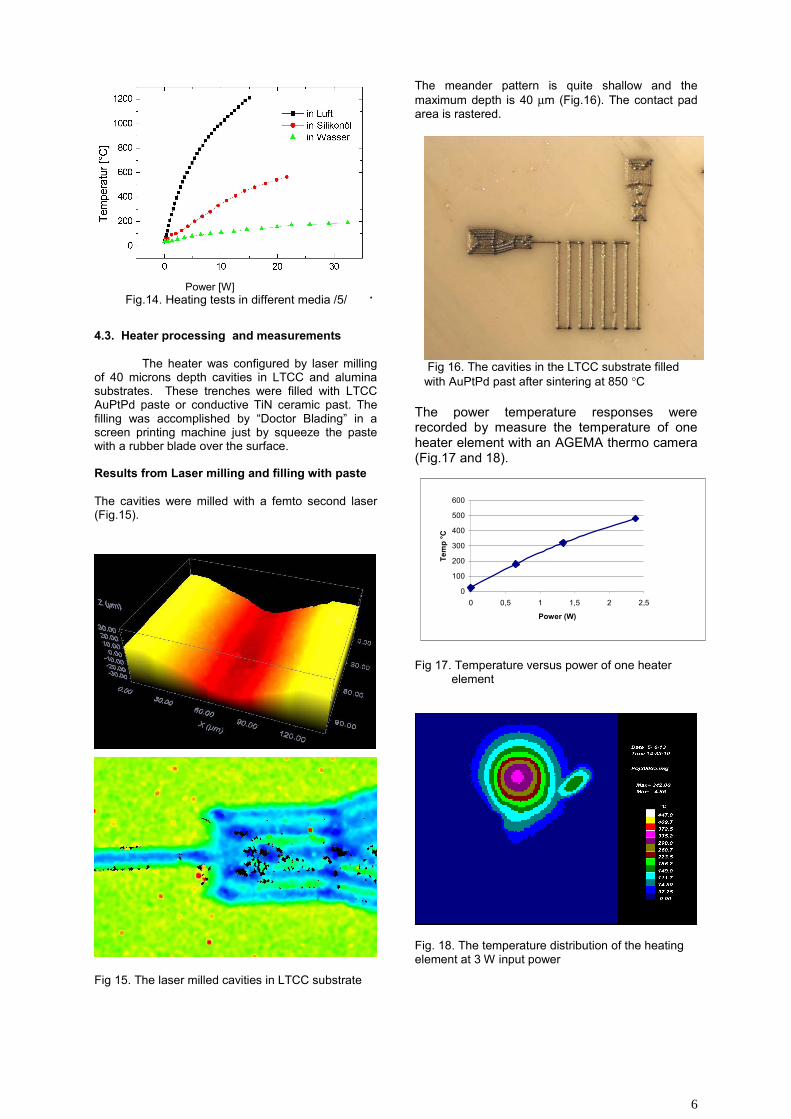
. 4.3. Heater processing and measurements The heater was configured by laser milling of 40 microns depth cavities in LTCC and alumina substrates. These trenches were filled with LTCC AuPtPd paste or conductive TiN ceramic past. The filling was accomplished by “Doctor Blading” in a screen printing machine just by squeeze the paste with a rubber blade over the surface. Results from Laser milling and filling with paste The cavities were milled with a femto second laser (Fig.15).
Fig 15. The laser milled cavities in LTCC substrate
The meander pattern is quite shallow and the maximum depth is 40 µm (Fig.16). The contact pad area is rastered.
Fig 16. The cavities in the LTCC substrate filled with AuPtPd past after sintering at 850 °C
The power temperature responses were recorded by measure the temperature of one heater element with an AGEMA thermo camera (Fig.17 and 18).
0
100
200
300
400
500
600
0 0,5 1 1,5 2 2,5
Power (W)
Tem
p °C
Fig 17. Temperature versus power of one heater element
Fig. 18. The temperature distribution of the heating element at 3 W input power
Power [W] Fig.14. Heating tests in different media /5/
6
5. Conclusions
The purpose of the work was to establish a fabrication technology for realising gas sensors on ceramic substrates by combining a range of processing techniques. The gas sensor design and manufacturing methodology described in the paper will act as a demonstrator for the realisation of this technology.
The main goal/overall objective is to obtain miniaturized, low cost devices on non-silicon substrates, with high sensitivity and low power consumption to be used in portable devices.
The mixed technologies method discussed here, allowing the generation of new type of sensors with existing tools (software, technological facilities, etc) represents an added value at European level.
New areas as System in Package will be investigated for realising the integration on the same package of a sensor array and electronics.
Acknowledgements The authors express the acknowledgements to the 4M NoE for supporting the work described in this paper. All results have been obtained in the frame of 4M, WP8 (Ceramic Cluster) .
References [1] Julian W. Gardner, Philip N. Bartlett; Electronic Noses - Principles and Applications, Oxford University Press, 1999, pp 67-110 [2] RF Taylor, JS Schultz, Handbook of Chemical and Biological Sensors, Institute of Physics Publishing Bristol and Philadelphia, 1996, pp. 371-394 [3] Kaufmann, U.; Ritzhaupt-Kleissl, H.-J.:-Multicomponent Ceramic Heaters. St.Louis, Mo 104th Annual Meeting of the Amer. Ceramic Society, 1 May 2002 [4] Kaufmann, U.; Haußelt, J.; Moritz, H. Fast Fabrication of Ceramic Microcomponents.- MST News.- No 4/01.-September 2001 S. 35-38 [5] Stolz, S.: Screen printing of electro-conductive ceramic for the development of microheater devices.-Research Report FZKA 6906.-2004
7