Embed Size (px)
Citation preview
G.TARONI Les Mémoires Mortes Les MémoiresMortes Programmables
Microelectronics ESSONNESCD LAB
Mémoires mortes
Mémoires mortes programmables&
G.TARONI Les Mémoires Mortes Les MémoiresMortes Programmables
Microelectronics ESSONNESCD LAB
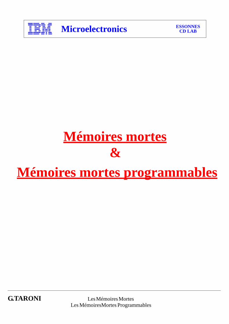
Cellule ROM
Point mémoire présent = “0”
Point mémoire absent = “1”
Ligne de Bit
Ligne de Mot
G.TARONI Les Mémoires Mortes Les MémoiresMortes Programmables
Microelectronics ESSONNESCD LAB
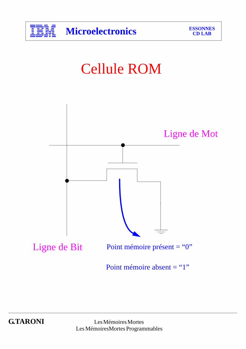
Cellule à personnalisation oxyde(Early Perso)
G.TARONI Les Mémoires Mortes Les MémoiresMortes Programmables
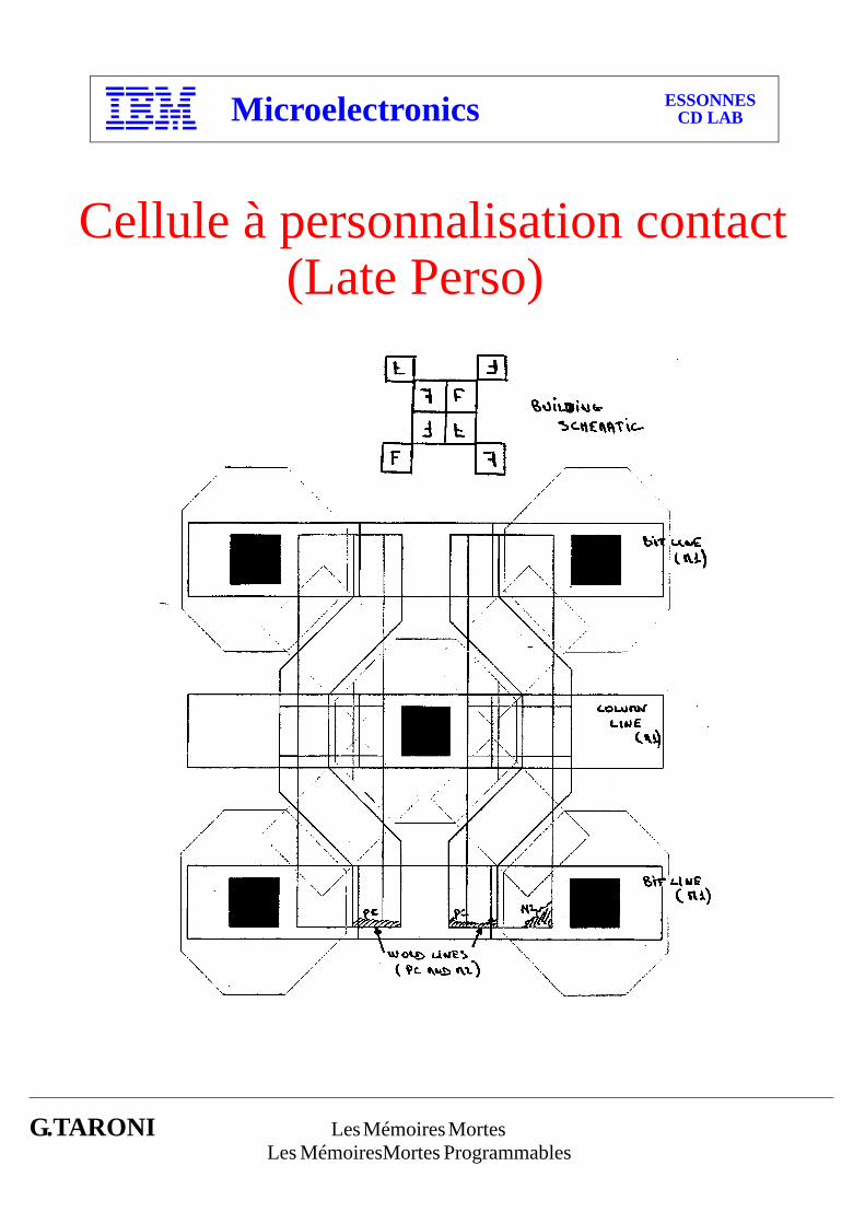
Microelectronics ESSONNESCD LAB
Cellule à personnalisation contact(Late Perso)
G.TARONI Les Mémoires Mortes Les MémoiresMortes Programmables
Microelectronics ESSONNESCD LAB
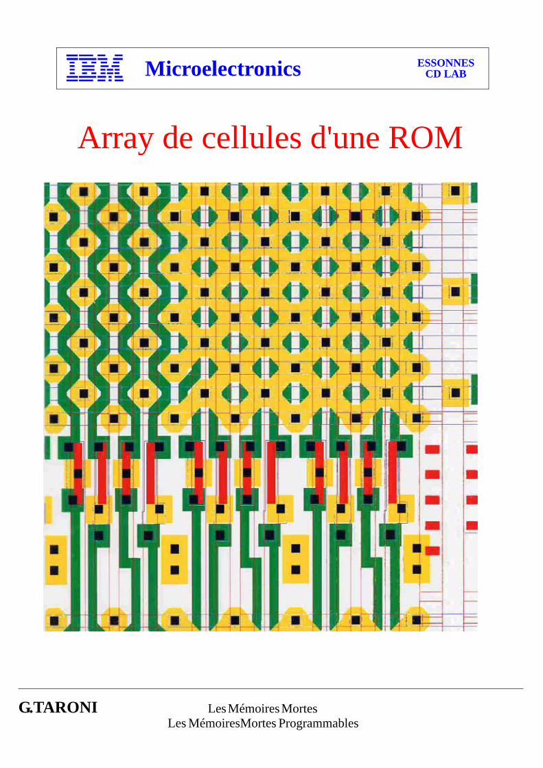
Array de cellules d'une ROM
G.TARONI Les Mémoires Mortes Les MémoiresMortes Programmables
Microelectronics ESSONNESCD LAB
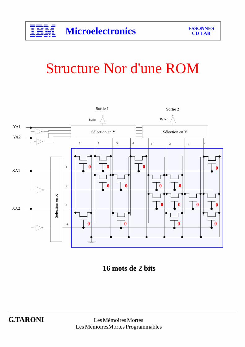
Structure Nor d'une ROM
Sélection en Y Sélection en Y
Buffer Buffer
Sortie 1 Sortie 2
Séle
ctio
n en
X
XA2
XA1
YA2
YA1
1 2 3 4 1 2 3 4
1
2
3
4
0 0 0
0 0 0
0 0 0
0 0 0 0
0
0
0
16 mots de 2 bits
G.TARONI Les Mémoires Mortes Les MémoiresMortes Programmables
Microelectronics ESSONNESCD LAB
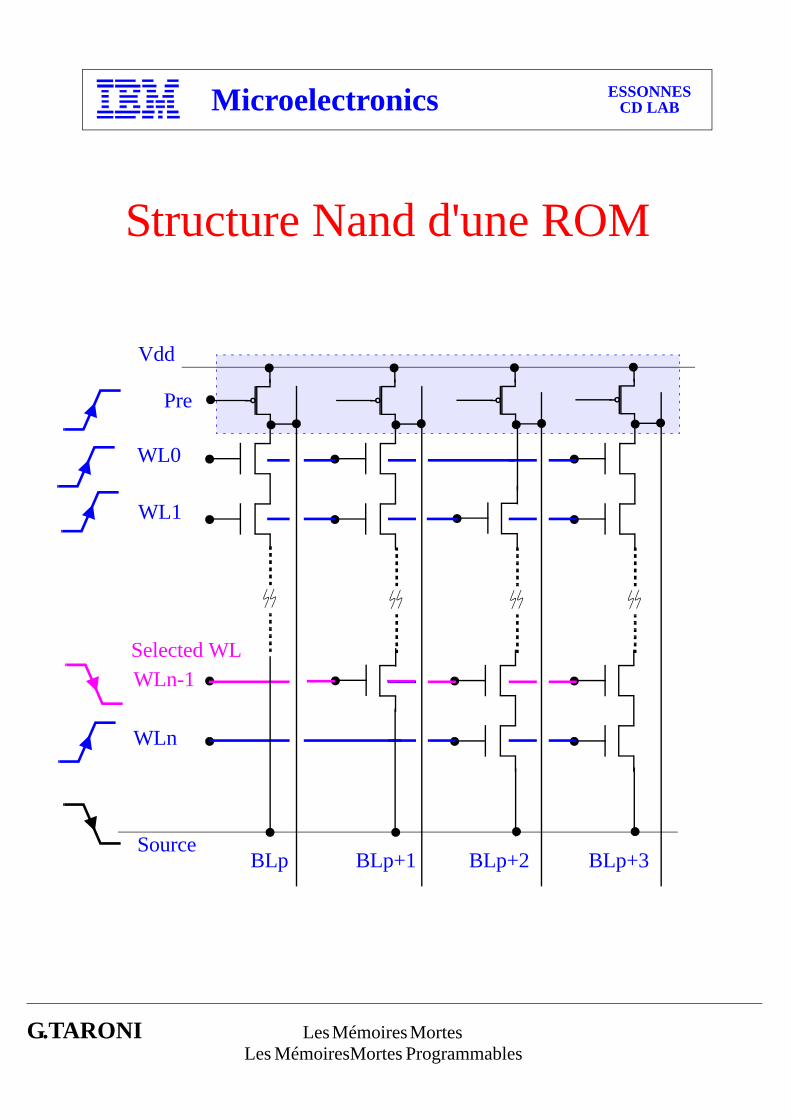
Structure Nand d'une ROM
WL0
WL1
WLn
BLp
WLn-1
Source
Pre
BLp+1 BLp+2 BLp+3
Vdd
Selected WL
G.TARONI Les Mémoires Mortes Les MémoiresMortes Programmables
Microelectronics ESSONNESCD LAB
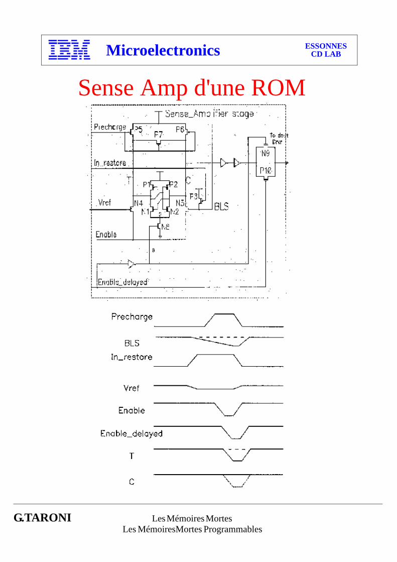
Sense Amp d'une ROM
G.TARONI Les Mémoires Mortes Les MémoiresMortes Programmables
Microelectronics ESSONNESCD LAB
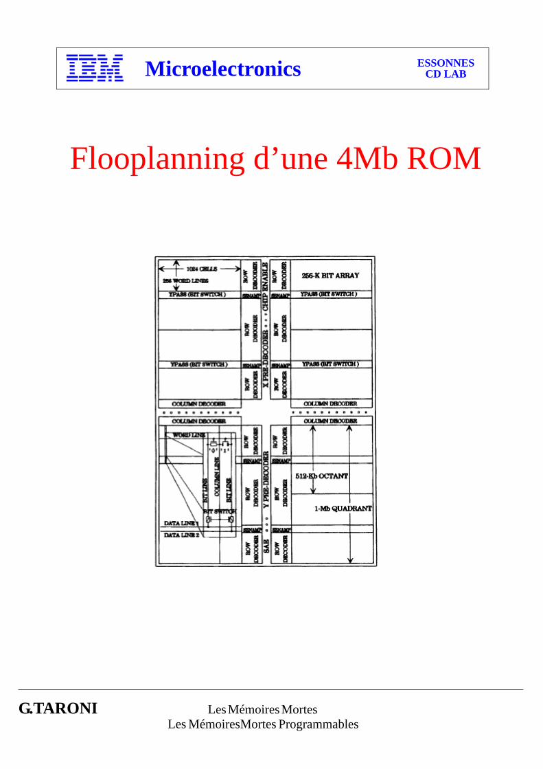
Flooplanning d’une 4Mb ROM
G.TARONI Les Mémoires Mortes Les MémoiresMortes Programmables
Microelectronics ESSONNESCD LAB
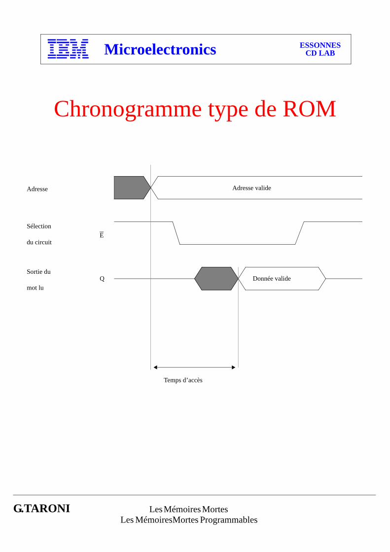
Chronogramme type de ROM
Adresse Adresse valide
Sélection
du circuit
Sortie du
mot lu
E
Q
Temps d’accès
Donnée valide
G.TARONI Les Mémoires Mortes Les MémoiresMortes Programmables
Microelectronics ESSONNESCD LAB
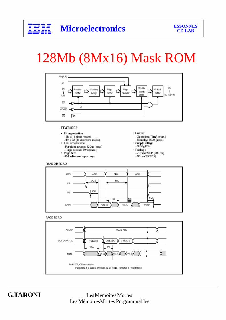
128Mb (8Mx16) Mask ROM
G.TARONI Les Mémoires Mortes Les MémoiresMortes Programmables
Microelectronics ESSONNESCD LAB
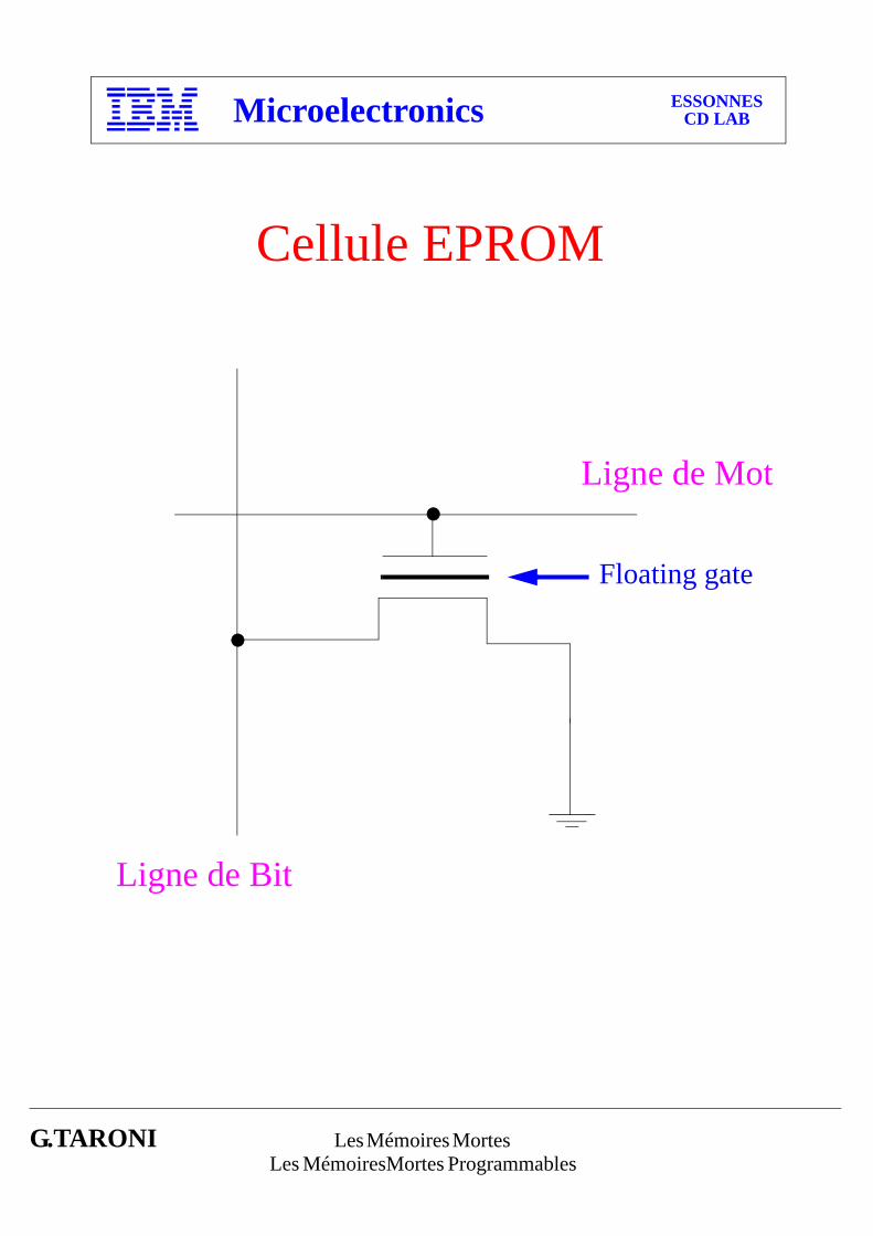
Cellule EPROM
Ligne de Bit
Ligne de Mot
Floating gate
G.TARONI Les Mémoires Mortes Les MémoiresMortes Programmables
Microelectronics ESSONNESCD LAB
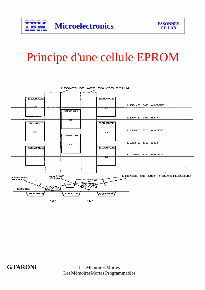
Principe d'une cellule EPROM
G.TARONI Les Mémoires Mortes Les MémoiresMortes Programmables
Microelectronics ESSONNESCD LAB
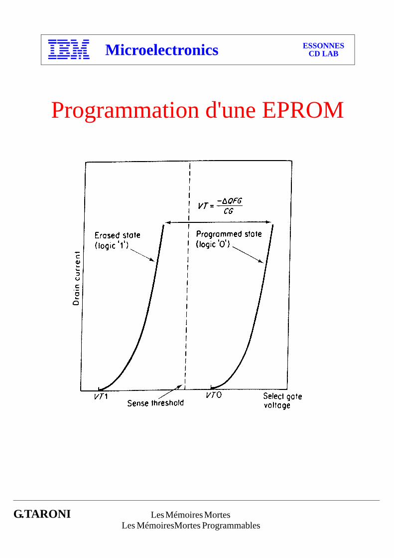
Programmation d'une EPROM
G.TARONI Les Mémoires Mortes Les MémoiresMortes Programmables
Microelectronics ESSONNESCD LAB
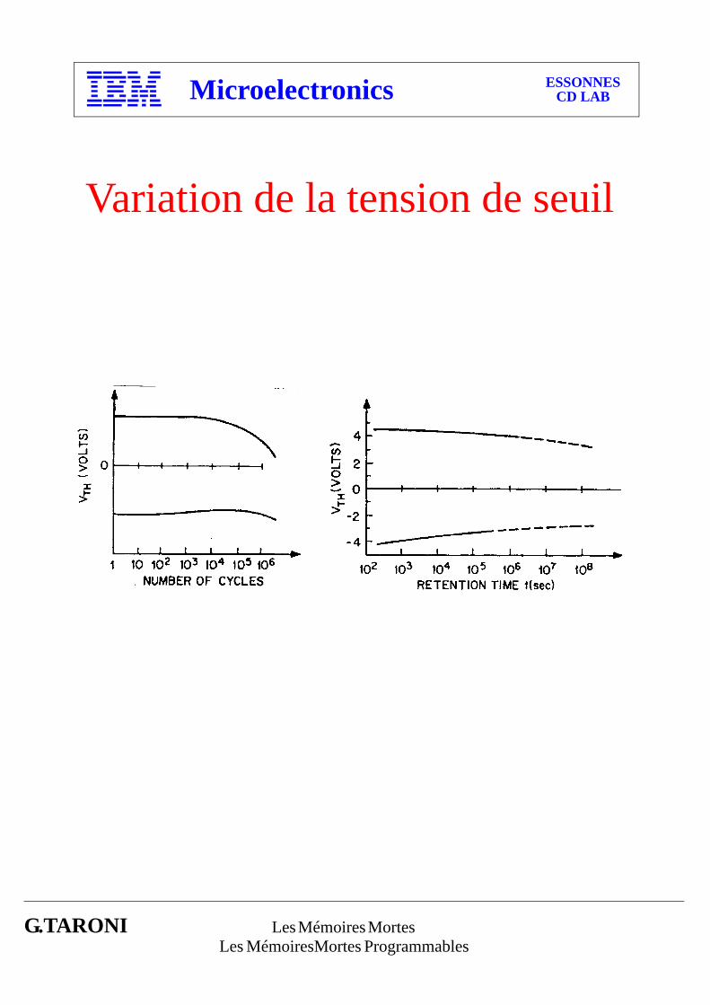
Variation de la tension de seuil
G.TARONI Les Mémoires Mortes Les MémoiresMortes Programmables
Microelectronics ESSONNESCD LAB
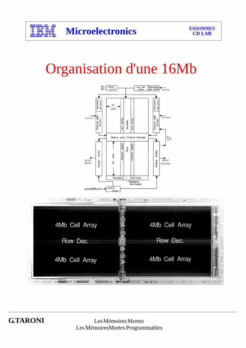
Organisation d'une 16Mb
G.TARONI Les Mémoires Mortes Les MémoiresMortes Programmables
Microelectronics ESSONNESCD LAB
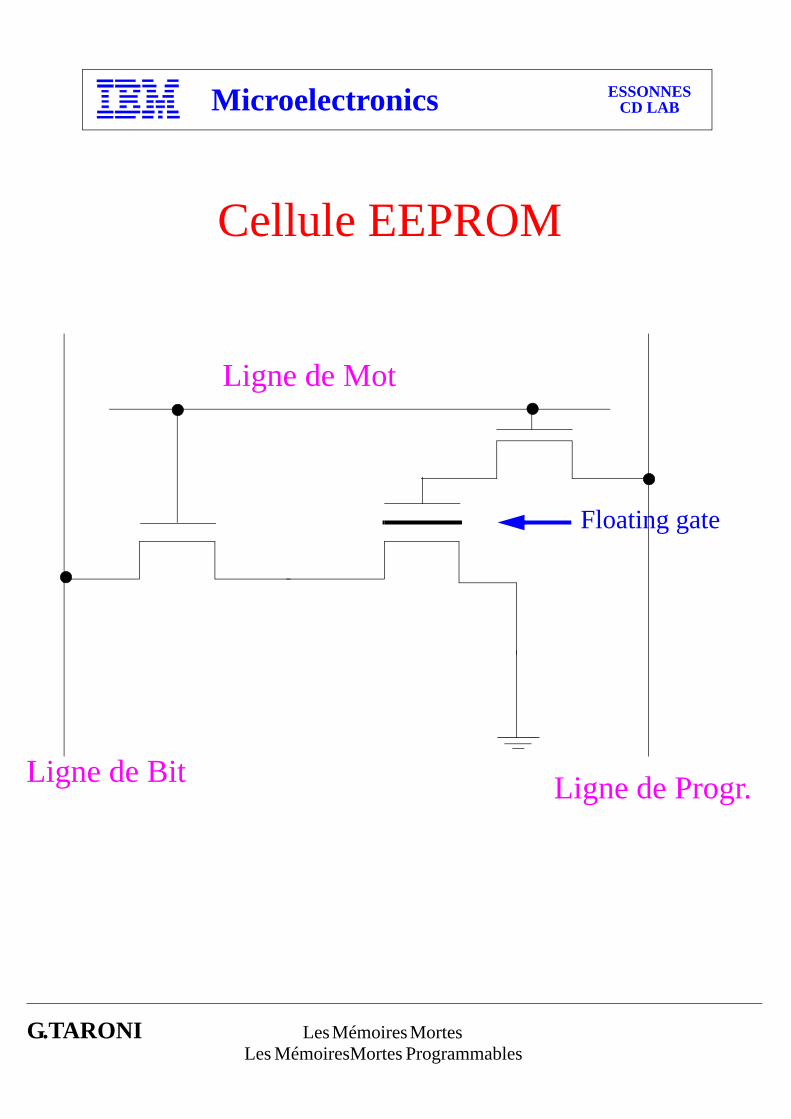
Cellule EEPROM
Ligne de Bit Ligne de Progr.
Floating gate
Ligne de Mot
G.TARONI Les Mémoires Mortes Les MémoiresMortes Programmables
Microelectronics ESSONNESCD LAB
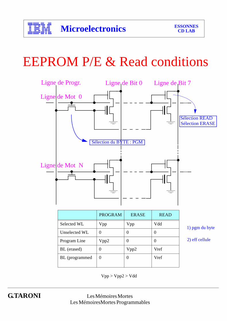
Ligne de Mot 0
Ligne de Mot N
Ligne de Bit 0 Ligne de Bit 7Ligne de Progr.
Sélection du BYTE : PGM
EEPROM P/E & Read conditions
PROGRAM ERASE READ
Selected WL Vpp Vpp Vdd
Unselected WL 0 0 0
Program Line Vpp2 0 0
BL (erased) 0 Vpp2 Vref
BL (programmed 0 0 Vref
Sélection READSélection ERASE
Vpp > Vpp2 > Vdd
1) pgm du byte
2) eff cellule
G.TARONI Les Mémoires Mortes Les MémoiresMortes Programmables
Microelectronics ESSONNESCD LAB
Sortie valide
Adresses Adresses valides
CE
OE
SortieHaute impédance
Temps d’accès
Donnée valide
à l’entrée
Donnée valide
en lecture
Donnée pour
adresse suivante
CE / VPP
OE
Q0-7
A0-1
Programmation Vérification
Adresse Adresse suivante
Chronogramme de programmation
Chronogramme de lecture
G.TARONI Les Mémoires Mortes Les MémoiresMortes Programmables
Microelectronics ESSONNESCD LAB
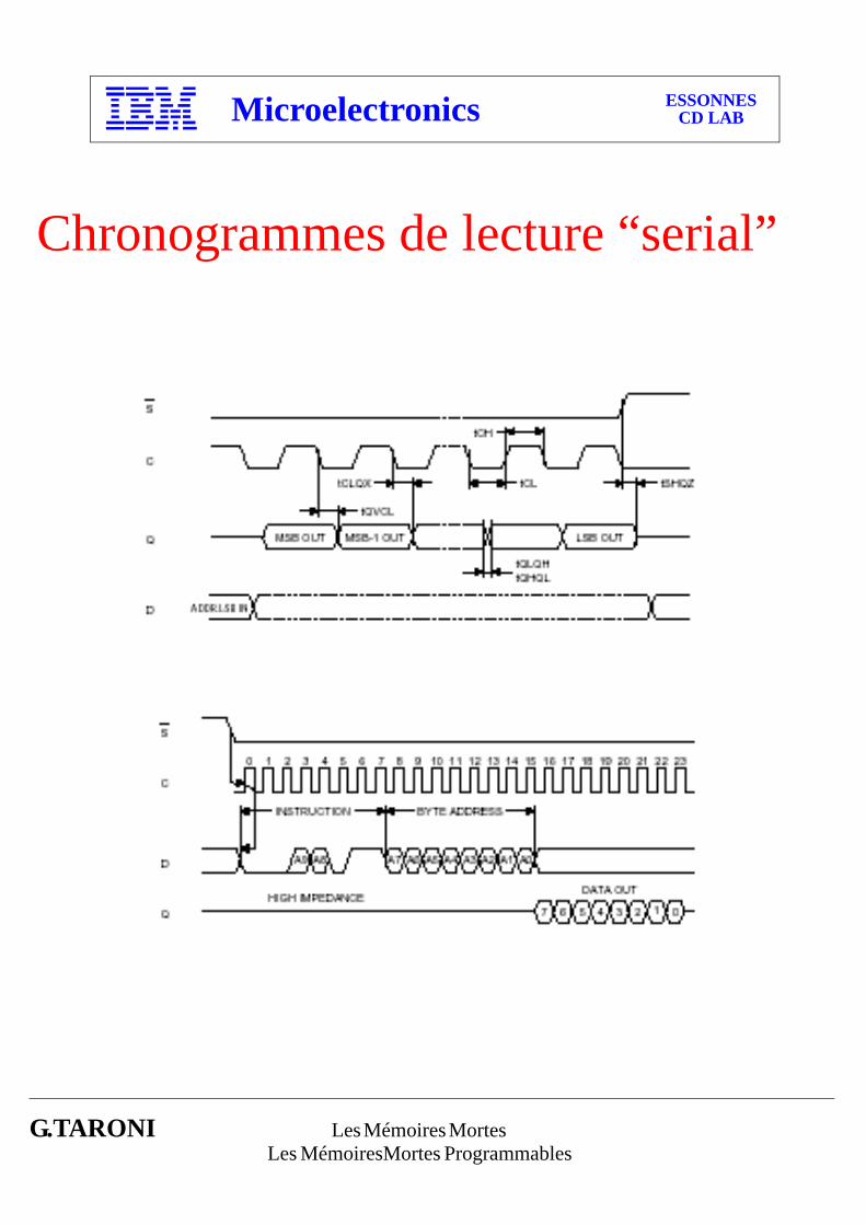
Chronogrammes de lecture “serial”
G.TARONI Les Mémoires Mortes Les MémoiresMortes Programmables
Microelectronics ESSONNESCD LAB
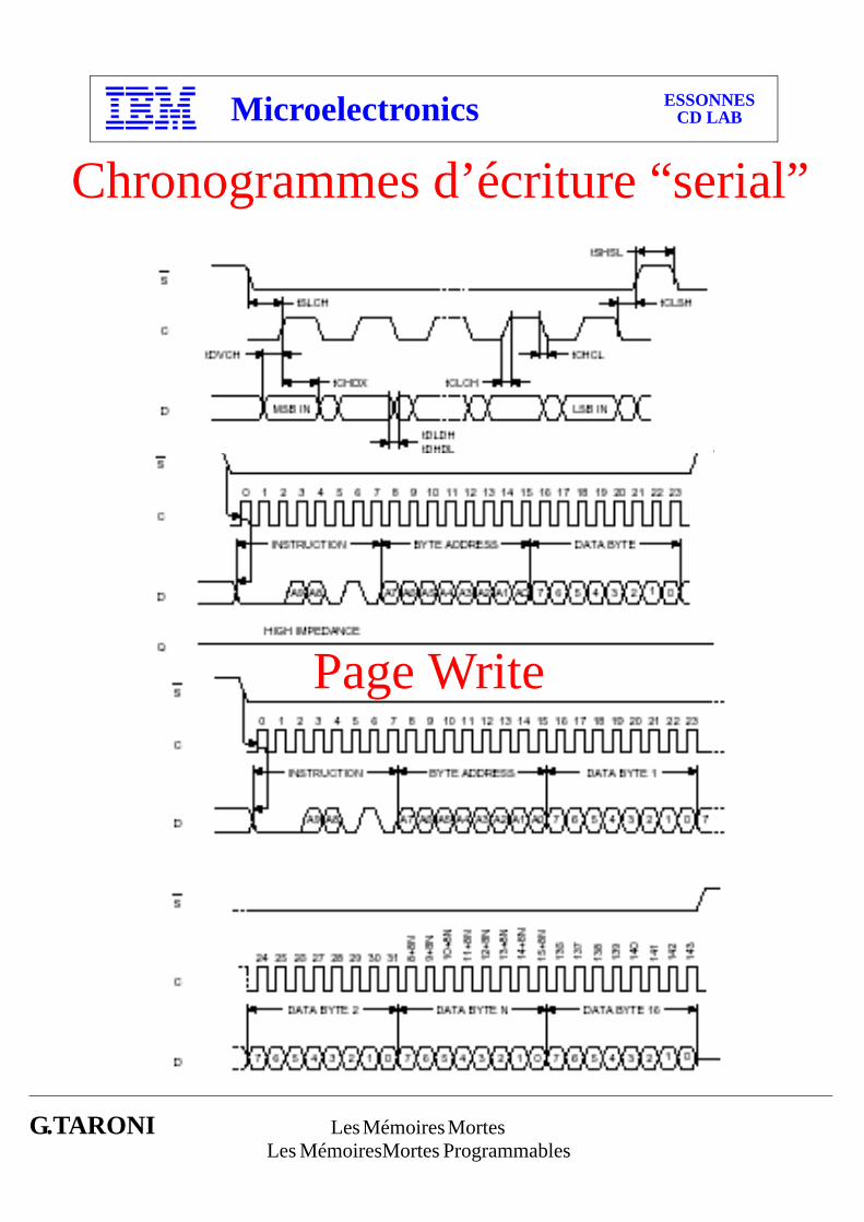
Chronogrammes d’écriture “serial”
Page Write
G.TARONI Les Mémoires Mortes Les MémoiresMortes Programmables
Microelectronics ESSONNESCD LAB
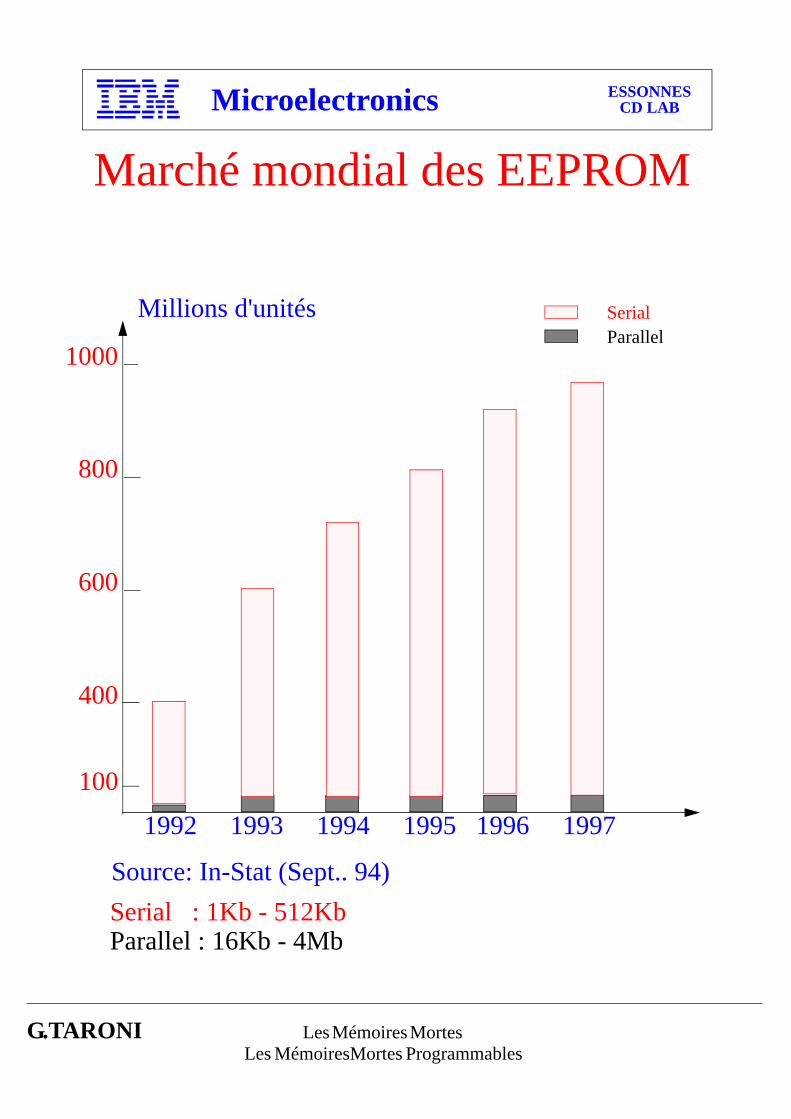
Marché mondial des EEPROM
Millions d'unités
1992 1993 1994 1995 1996 1997
Source: In-Stat (Sept.. 94)
400
600
800
1000ParallelSerial
100
Serial : 1Kb - 512KbParallel : 16Kb - 4Mb
G.TARONI Les Mémoires Mortes Les MémoiresMortes Programmables
Microelectronics ESSONNESCD LAB
G.TARONI Les Mémoires Mortes Les MémoiresMortes Programmables
Microelectronics ESSONNESCD LAB
G.TARONI Les Flash (E)eprom
Microelectronics ESSONNESCD LAB
Les Flash (E)EPROM
G.TARONI Les Flash (E)eprom
Microelectronics ESSONNESCD LAB
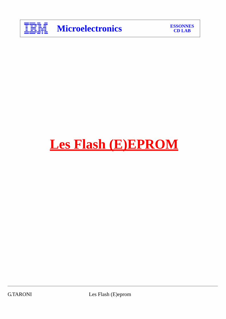
• AUTOMOBILES : Controle Moteur, ABS, AIRBAG, Instrumentation,Navigation,...
• COMMUNICATIONS : Telephone portable, sans fil , Pager, Talkie-Walkie, Set-up box, Console de jeux , ...
• GRANDE CONSOMMATION : CAMERA, CAMESCOPE, ENREGIS-TREUR AUDIO, ...
• BUREAUTIQUES : Printer Laser, a jet d’encre, Driver disque dur, Photo-copieur, Disque dur, PDA, ...
• INDUSTRIELLES : Controle Robotiques / Servo / Moteurs, Lecteur codebarres, ...
Applications...
G.TARONI Les Flash (E)eprom
Microelectronics ESSONNESCD LAB
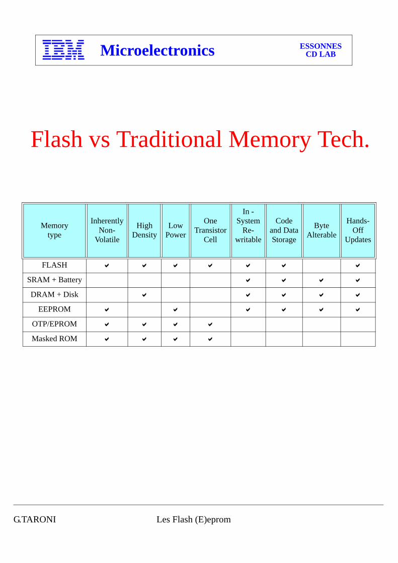
Flash vs Traditional Memory Tech.
Memorytype
InherentlyNon-
Volatile
HighDensity
LowPower
One Transistor
Cell
In -System
Re-writable
Code and DataStorage
Byte Alterable
Hands-Off
Updates
FLASH
SRAM + Battery
DRAM + Disk
EEPROM
OTP/EPROM
Masked ROM
G.TARONI Les Flash (E)eprom
Microelectronics ESSONNESCD LAB
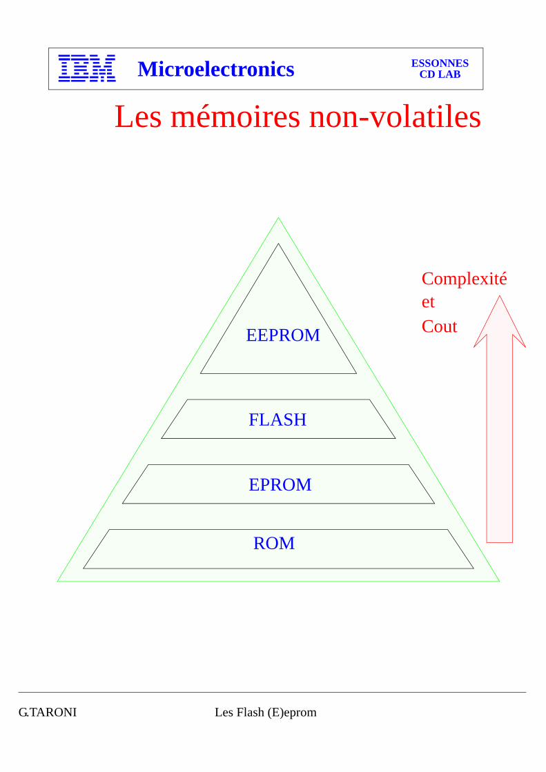
Les mémoires non-volatiles
EEPROM
FLASH
EPROM
ROM
Complexité et Cout
G.TARONI Les Flash (E)eprom
Microelectronics ESSONNESCD LAB
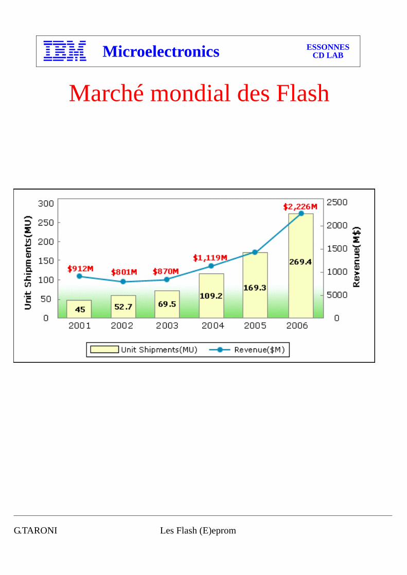
Marché mondial des Flash
G.TARONI Les Flash (E)eprom
Microelectronics ESSONNESCD LAB
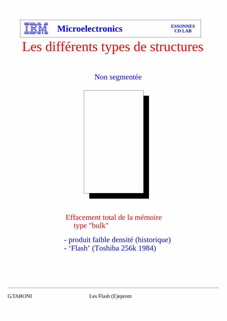
Non segmentée
Effacement total de la mémoire type "bulk"
Les différents types de structures
- produit faible densité (historique)- ‘Flash’ (Toshiba 256k 1984)
G.TARONI Les Flash (E)eprom
Microelectronics ESSONNESCD LAB
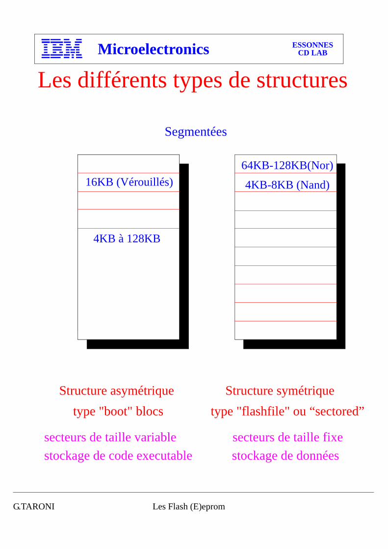
Segmentées
Structure asymétrique type "boot" blocs
Les différents types de structures
secteurs de taille variablestockage de code executable
Structure symétrique type "flashfile" ou “sectored”
secteurs de taille fixestockage de données
64KB-128KB(Nor)16KB (Vérouillés)
4KB à 128KB
4KB-8KB (Nand)
G.TARONI Les Flash (E)eprom
Microelectronics ESSONNESCD LAB
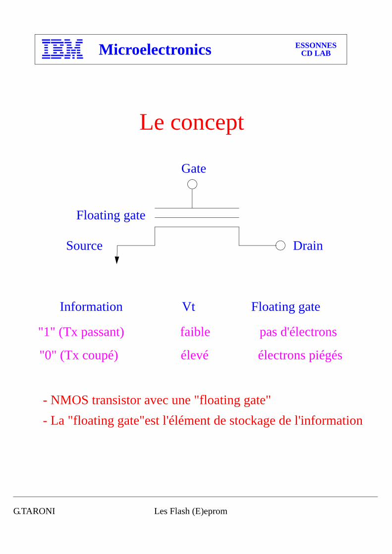
Drain
Le concept
Source
Gate
Floating gate
Information Vt Floating gate
"1" (Tx passant) faible pas d'électrons
"0" (Tx coupé) élevé électrons piégés
- NMOS transistor avec une "floating gate"- La "floating gate"est l'élément de stockage de l'information
G.TARONI Les Flash (E)eprom
Microelectronics ESSONNESCD LAB
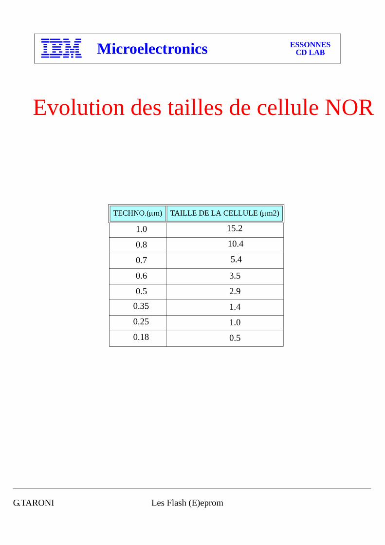
TECHNO.(µm) TAILLE DE LA CELLULE (µm2)
1.0 15.2
0.8 10.4
0.7 5.4
0.6 3.5
0.5 2.9 0.35 1.4 0.25 1.0 0.18 0.5
Evolution des tailles de cellule NOR
G.TARONI Les Flash (E)eprom
Microelectronics ESSONNESCD LAB
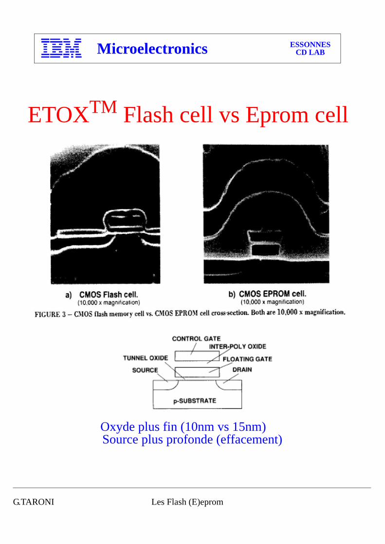
ETOXTM Flash cell vs Eprom cell
Oxyde plus fin (10nm vs 15nm)Source plus profonde (effacement)
G.TARONI Les Flash (E)eprom
Microelectronics ESSONNESCD LAB
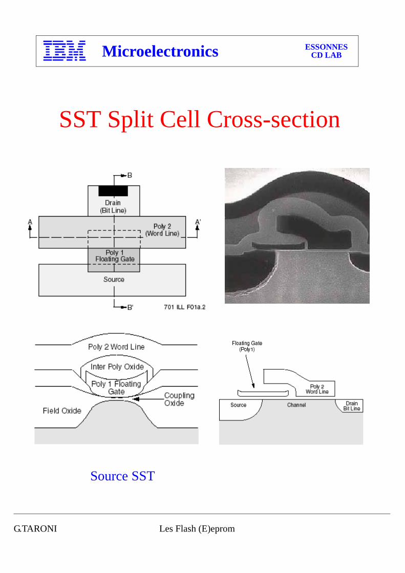
SST Split Cell Cross-section
Source SST
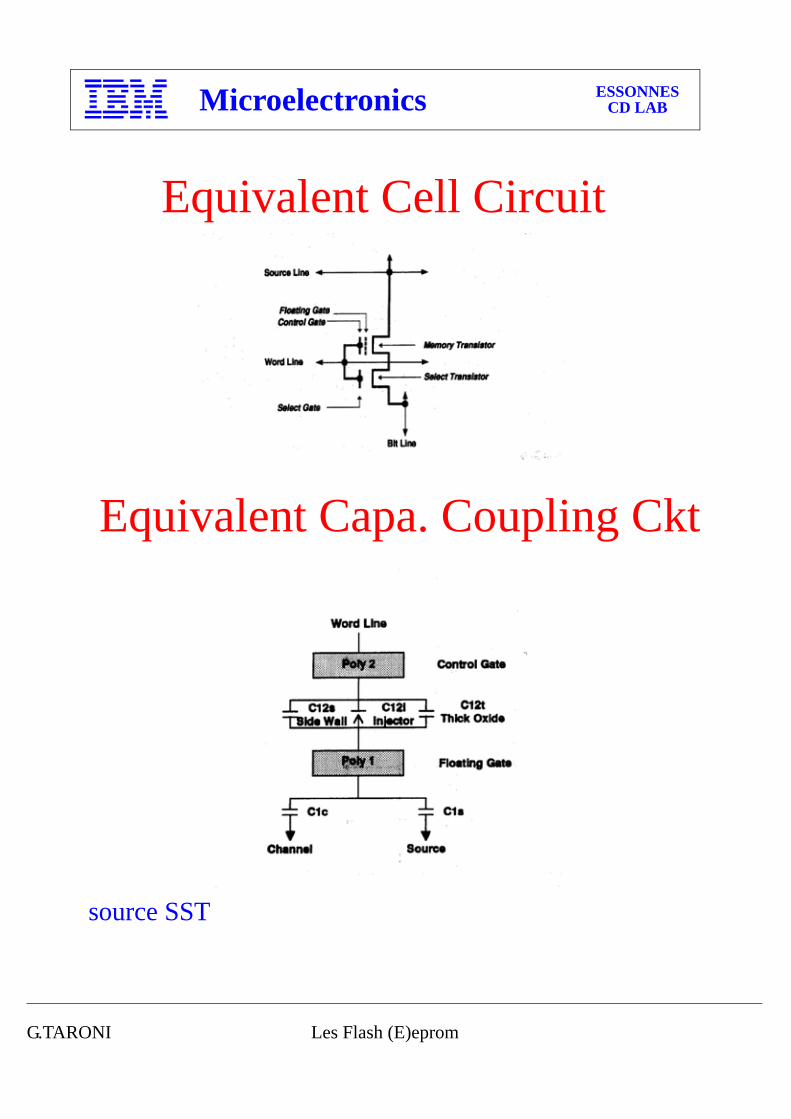
G.TARONI Les Flash (E)eprom
Microelectronics ESSONNESCD LAB
Equivalent Cell Circuit
source SST
Equivalent Capa. Coupling Ckt
G.TARONI Les Flash (E)eprom
Microelectronics ESSONNESCD LAB
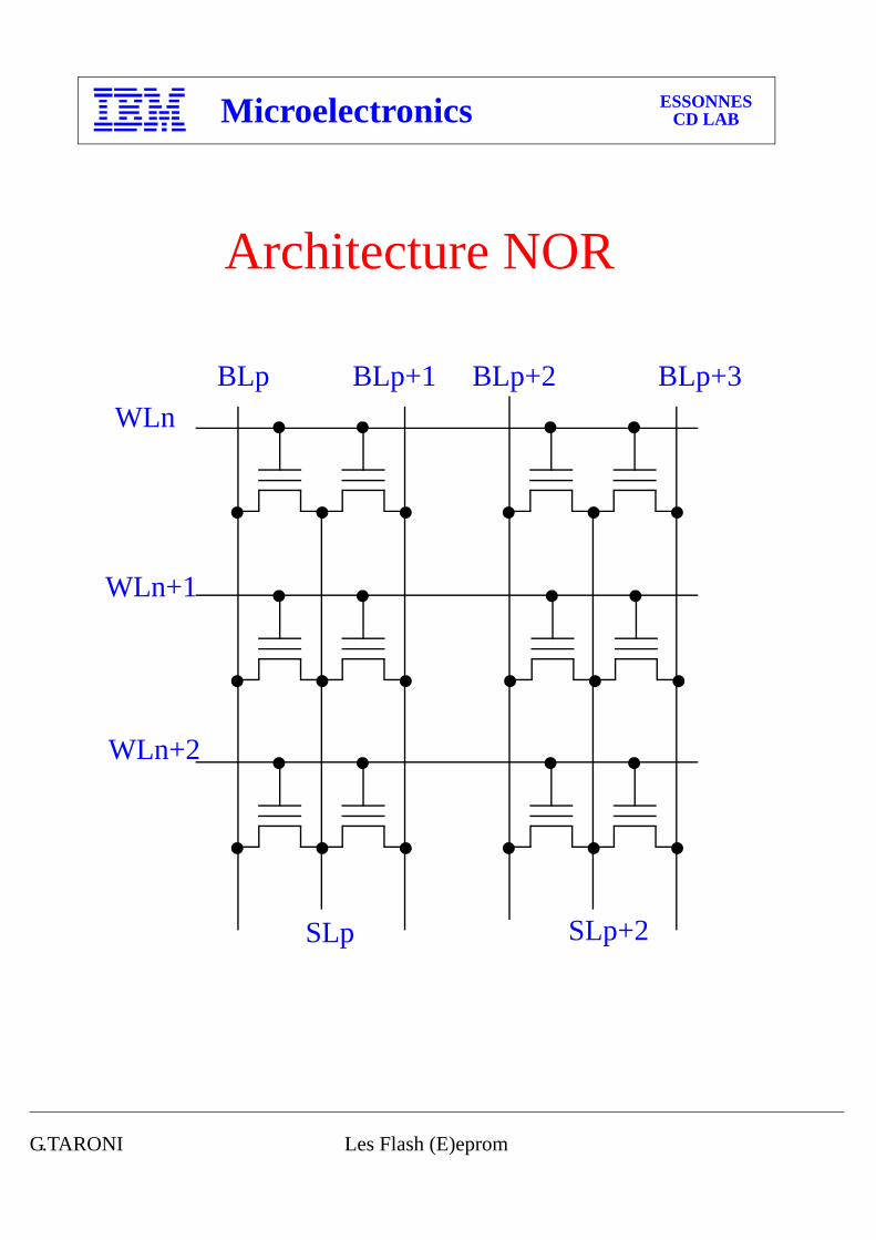
Architecture NOR
WLn
WLn+1
WLn+2
BLp BLp+1 BLp+2 BLp+3
SLp SLp+2
G.TARONI Les Flash (E)eprom
Microelectronics ESSONNESCD LAB
WL0
WL1
WL15
BLp
WL14
Source
Select Gate2
Select Gate1
BLp+1 BLp+2 BLp+3
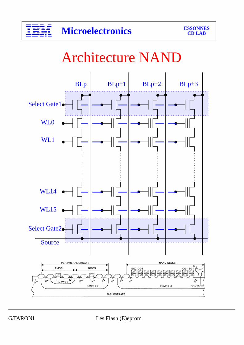
Architecture NAND
G.TARONI Les Flash (E)eprom
Microelectronics ESSONNESCD LAB
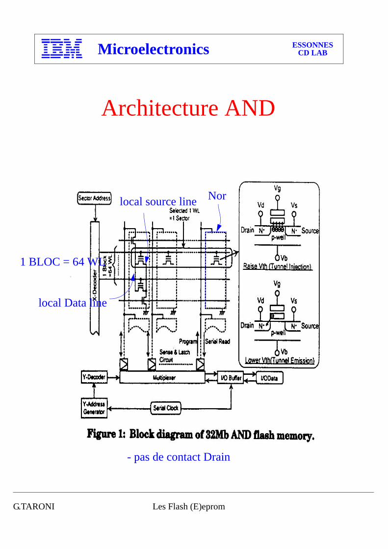
Architecture AND
1 BLOC = 64 WL
- pas de contact Drain
Nor
local Data line
local source line
G.TARONI Les Flash (E)eprom
Microelectronics ESSONNESCD LAB
Architecture DI-NOR
- diminution du RC (BL) - avantage structure NOR (Random access)- cellule plus petite : contact poly / diffusion et diffusion / métal
G.TARONI Les Flash (E)eprom
Microelectronics ESSONNESCD LAB
DI-NOR array
1 secteur = 1KB (512x16)
Sub BL
Main BL
M1
M2Poly
G.TARONI Les Flash (E)eprom
Microelectronics ESSONNESCD LAB
Architecture NAND
G.TARONI Les Flash (E)eprom
Microelectronics ESSONNESCD LAB
32Mb NAND (16x512x528 Octets)
G.TARONI Les Flash (E)eprom
Microelectronics ESSONNESCD LAB
Cellule Nand vs cellule Nor
Section de cellule Nand
Litho = 1µm
G.TARONI Les Flash (E)eprom
Microelectronics ESSONNESCD LAB
Tailles comparatives vs architecture
Cell Nor = 2.9 µm2Cell Nor = 3.5 µm2
G.TARONI Les Flash (E)eprom
Microelectronics ESSONNESCD LAB
N+ N+
Ck
Cs Cg Cd
Ct = Ck + Cs + Cg + Cd k = Ck / Ct (FG coupling ratio)
Control Gate
Floating Gate
Cellule FG
Diagramme des bandes d’énergie au repos
Equivalence des capacités de couplage
G.TARONI Les Flash (E)eprom
Microelectronics ESSONNESCD LAB
Programmation (Hot è)
DrainSource
Vpp
èèèèèèèèèèèè
N+ N+
VddGnd
è èè
è
Psub
Gnd
E > 3.2ev (Si/SiO2)
- modèle lucky électron : probabilité è d’être injectés
Diagramme des bandes d’énergie
G.TARONI Les Flash (E)eprom
Microelectronics ESSONNESCD LAB
Programmation (Hot è)
DrainSourceN+ N+
200A (20nm)
100A (10nm)
ONO
SiO2
Si
Tunnel Oxide
N+ N+
Ck
Cs Cg Cd
Ct = Ck + Cs + Cg + Cd + Csub k = Ck / Ct (FG coupling ratio)
Control Gate
Floating Gate
Polysilicon
Polysilicon
- Courant de programmation 4mA/byte env.- prgm < 10µs/byte env.
G.TARONI Les Flash (E)eprom
Microelectronics ESSONNESCD LAB
Programmation (Hot è) - Nor
G.TARONI Les Flash (E)eprom
Microelectronics ESSONNESCD LAB
Effacement (Fowler-Nordheim)
Drainèèèèèèèèèèèè
N+ N+
Vpp
Sourceè è
Psub
Gnd
Gnd
Standard (10 mA)
G.TARONI Les Flash (E)eprom
Microelectronics ESSONNESCD LAB
Effacement (Fowler-Nordheim)
Negative gate erase (10 µA) (AMD)
Drain
-Vpp
èèèèèèèèèèèè
N+ N+Source
Vdd
è è
- source moins profonde => taille plus petite- I Charge Pump plus petit => taille C.P. plus petite donc taille chip aussi
- Oxyde moins stressé => endurance accrue
G.TARONI Les Flash (E)eprom
Microelectronics ESSONNESCD LAB
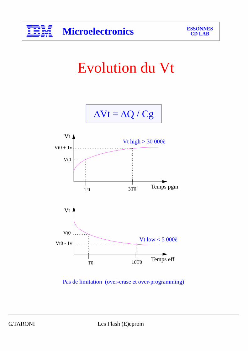
∆Vt = ∆Q / Cg
Vt low < 5 000è
Vt
Temps pgm
Vt
Temps eff
Pas de limitation (over-erase et over-programming)
Evolution du Vt
T0 3T0
Vt0
Vt high > 30 000èVt0 + 1v
T0 10T0
Vt0
Vt0 - 1v
G.TARONI Les Flash (E)eprom
Microelectronics ESSONNESCD LAB
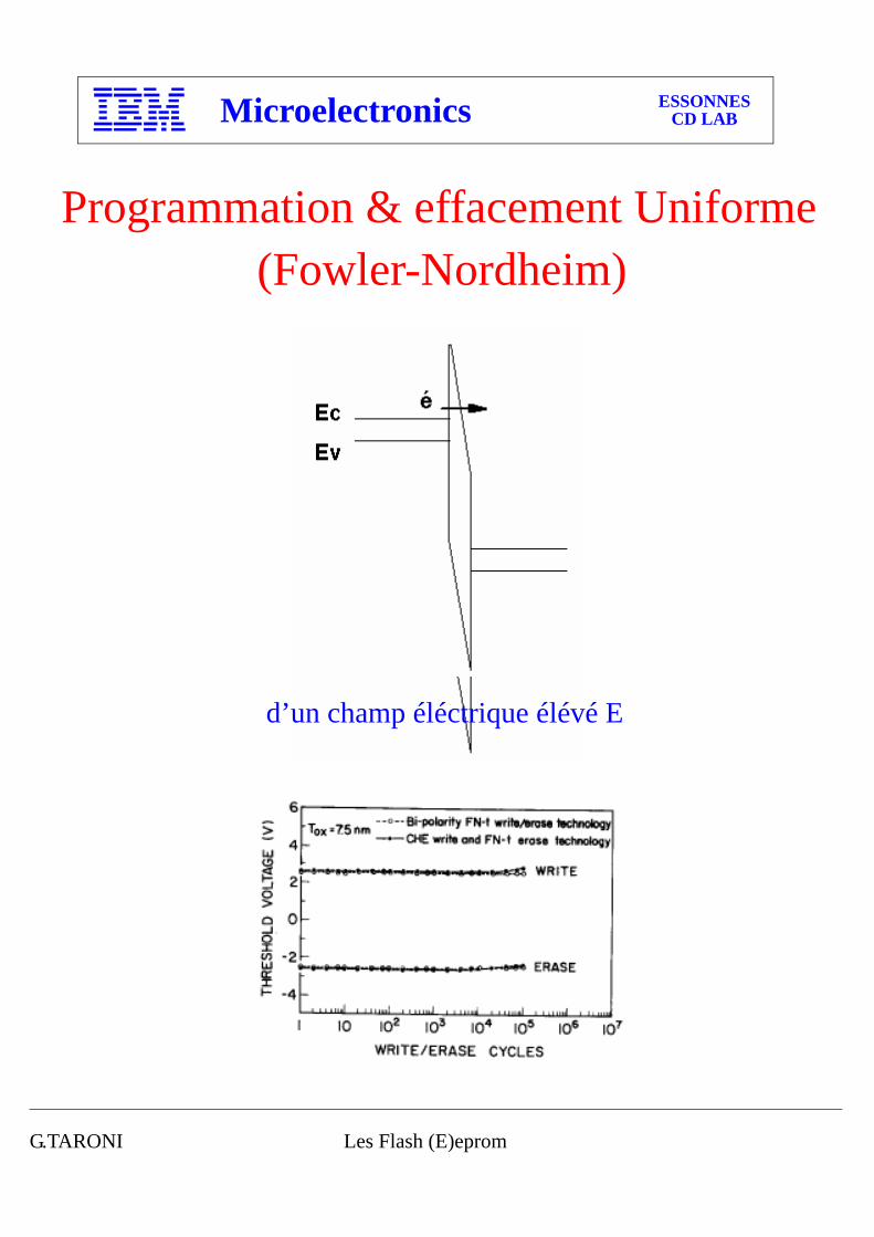
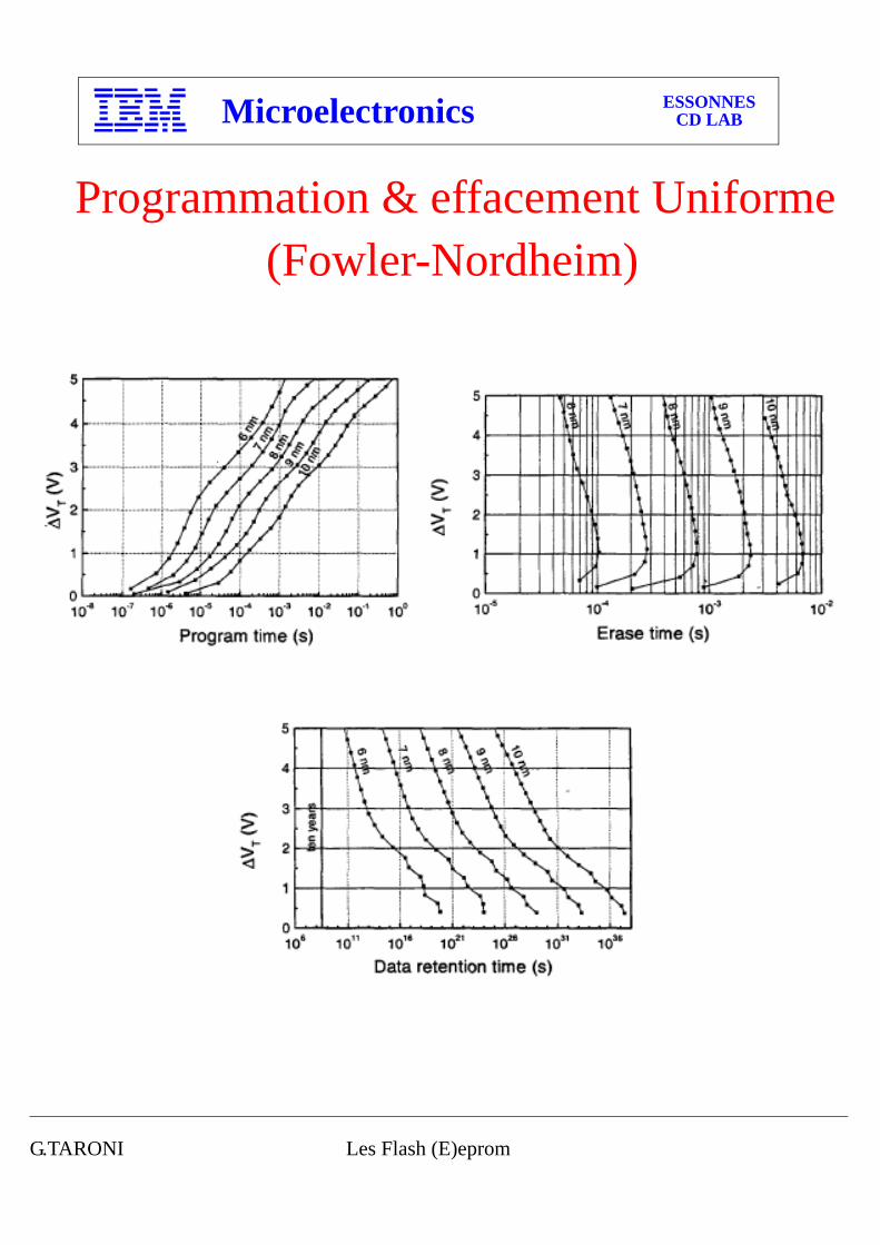
Programmation & effacement Uniforme(Fowler-Nordheim)
d’un champ éléctrique élévé E
G.TARONI Les Flash (E)eprom
Microelectronics ESSONNESCD LAB
E = V/tox
DrainSource
Vpp
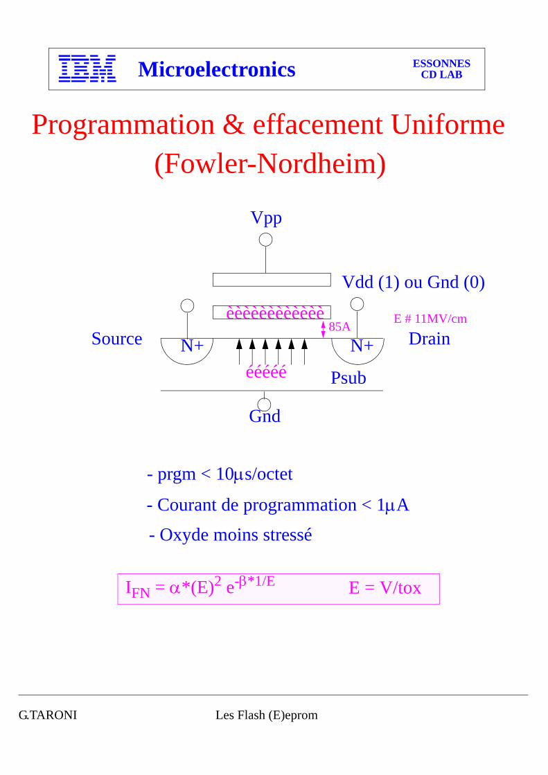
- Courant de programmation < 1µA
Programmation & effacement Uniforme(Fowler-Nordheim)
èèèèèèèèèèèè
N+ N+
Vdd (1) ou Gnd (0)
ééééé Psub
Gnd
E # 11MV/cm85A
IFN = α*(E)2 e-β*1/E
- prgm < 10µs/octet
- Oxyde moins stressé
G.TARONI Les Flash (E)eprom
Microelectronics ESSONNESCD LAB
Drain
Gnd
èèèèèèèèèèèè
N+ N+
Vdd
ééééé
Source
Psub
Vpp
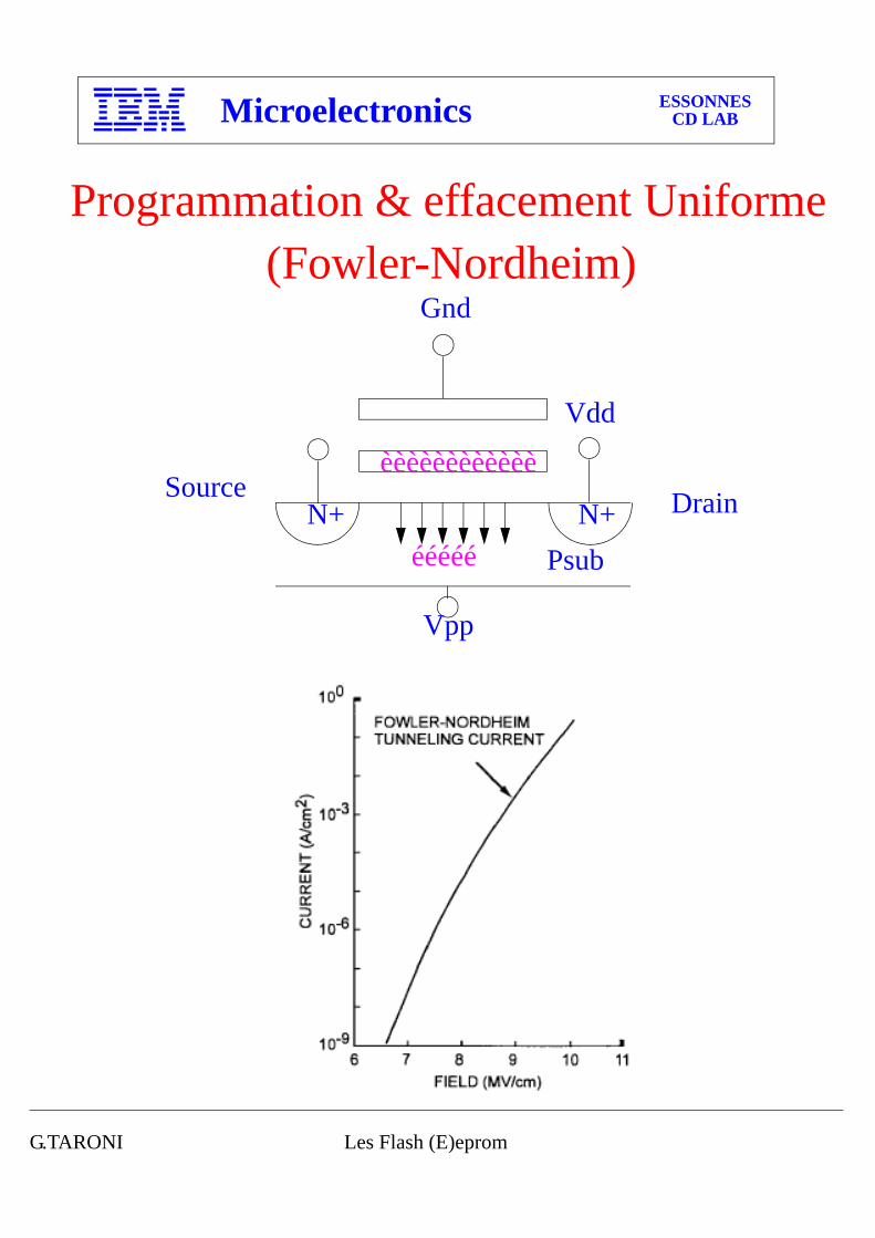
Programmation & effacement Uniforme(Fowler-Nordheim)
G.TARONI Les Flash (E)eprom
Microelectronics ESSONNESCD LAB
Programmation & effacement Uniforme(Fowler-Nordheim)
G.TARONI Les Flash (E)eprom
Microelectronics ESSONNESCD LAB
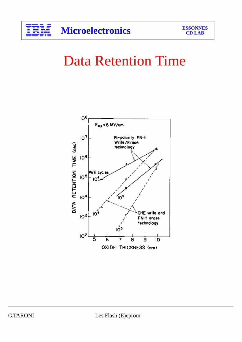
Data Retention Time
G.TARONI Les Flash (E)eprom
Microelectronics ESSONNESCD LAB
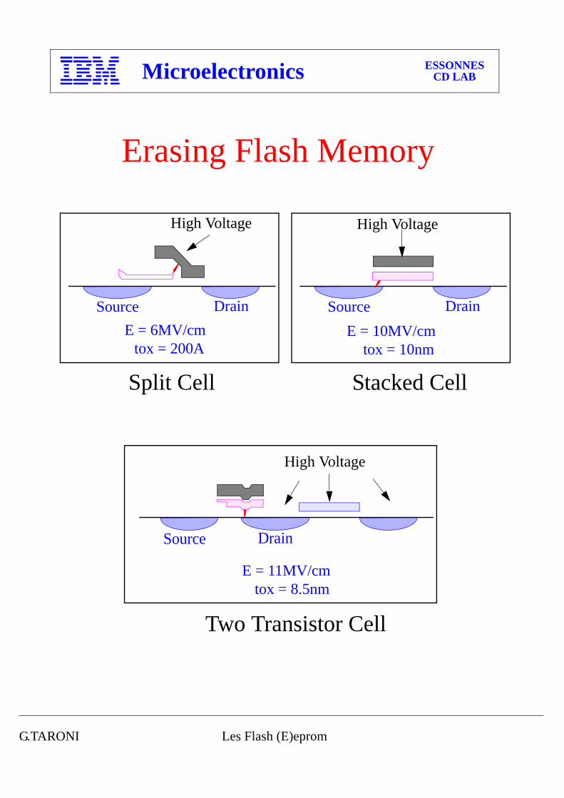
Erasing Flash Memory
DrainSource DrainSource
DrainSource
High Voltage
E = 6MV/cmtox = 200A
E = 10MV/cmtox = 10nm
High Voltage
E = 11MV/cmtox = 8.5nm
High Voltage
Split Cell Stacked Cell
Two Transistor Cell
G.TARONI Les Flash (E)eprom
Microelectronics ESSONNESCD LAB
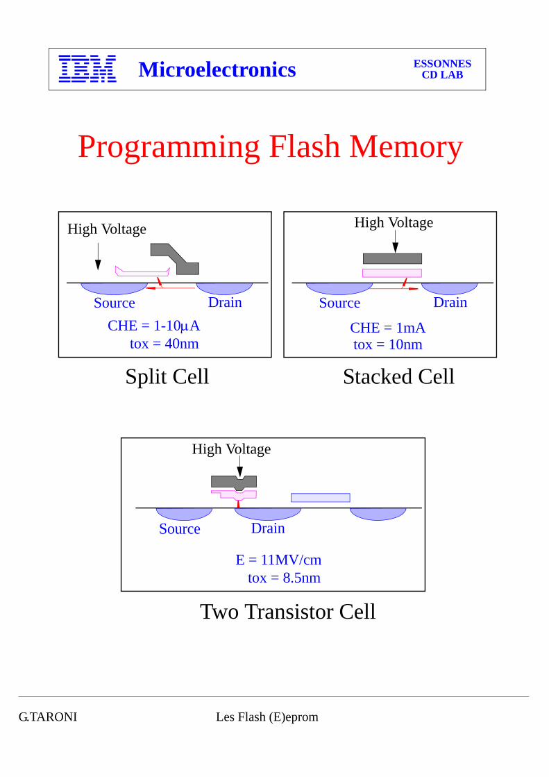
Programming Flash Memory
DrainSource DrainSource
DrainSource
High Voltage
CHE = 1-10µAtox = 40nm tox = 10nm
High Voltage
E = 11MV/cmtox = 8.5nm
High Voltage
CHE = 1mA
Split Cell Stacked Cell
Two Transistor Cell
G.TARONI Les Flash (E)eprom
Microelectronics ESSONNESCD LAB
0v
0v
15v
0v
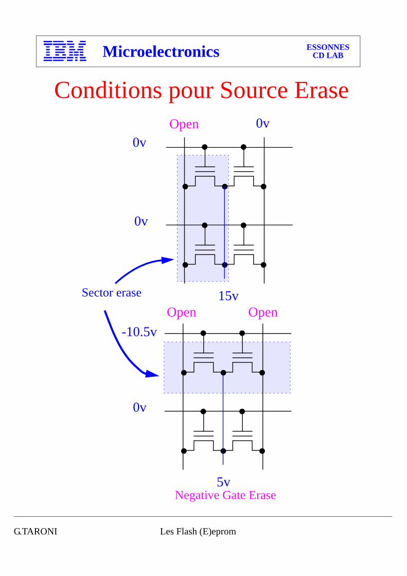
Conditions pour Source Erase Open
Sector erase
-10.5v
0v
5v
Open
Negative Gate Erase
Open
G.TARONI Les Flash (E)eprom
Microelectronics ESSONNESCD LAB
12v
0v
5v 0v
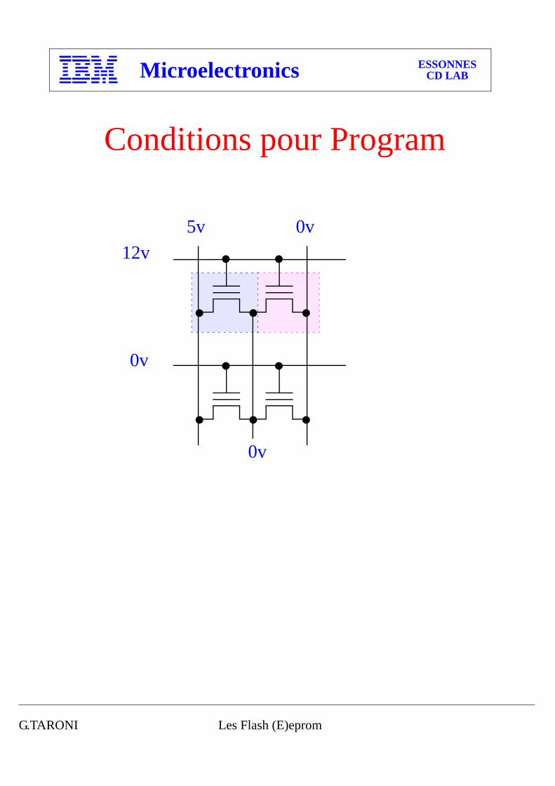
Conditions pour Program
0v
G.TARONI Les Flash (E)eprom
Microelectronics ESSONNESCD LAB
5v
0v
1v 0v
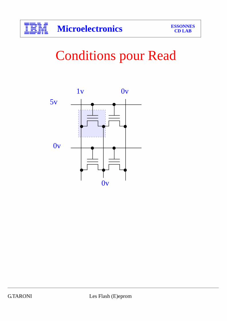
Conditions pour Read
0v
G.TARONI Les Flash (E)eprom
Microelectronics ESSONNESCD LAB
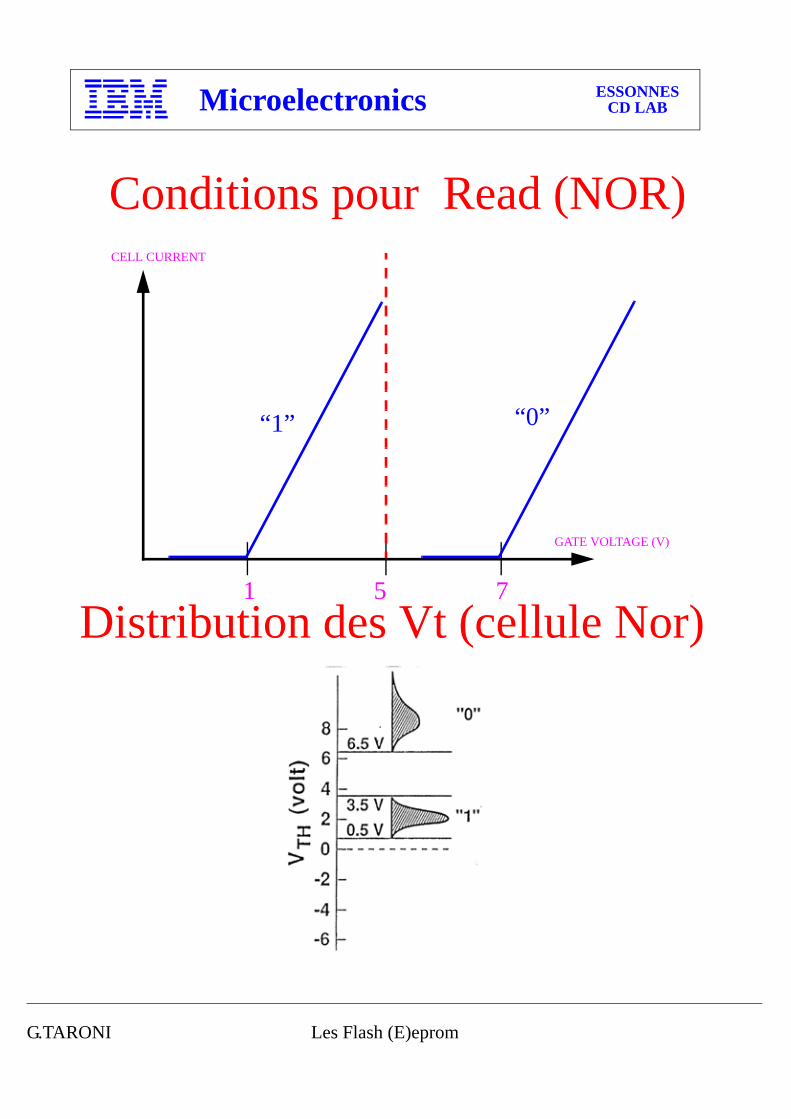
Conditions pour Read (NOR)
GATE VOLTAGE (V)
CELL CURRENT
“1” “0”
51 7Distribution des Vt (cellule Nor)
G.TARONI Les Flash (E)eprom
Microelectronics ESSONNESCD LAB
W L 0
W L 1
W L 1 5
W L 1 4
S o u rc e
S e l e c t G a t e 2
S e l e c t G a t e 1
Selected BL Unselected BL
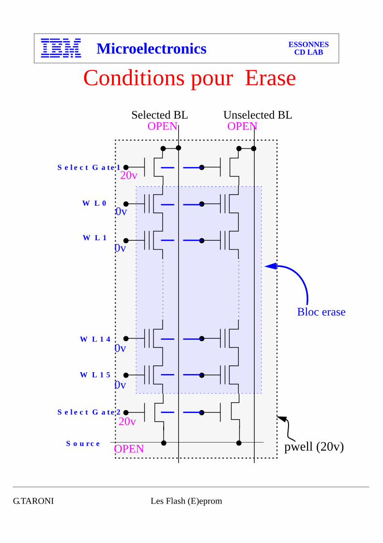
Conditions pour Erase
20v
OPEN OPEN
20v
0v
0v
0v
0v
OPEN
Bloc erase
pwell (20v)
G.TARONI Les Flash (E)eprom
Microelectronics ESSONNESCD LAB
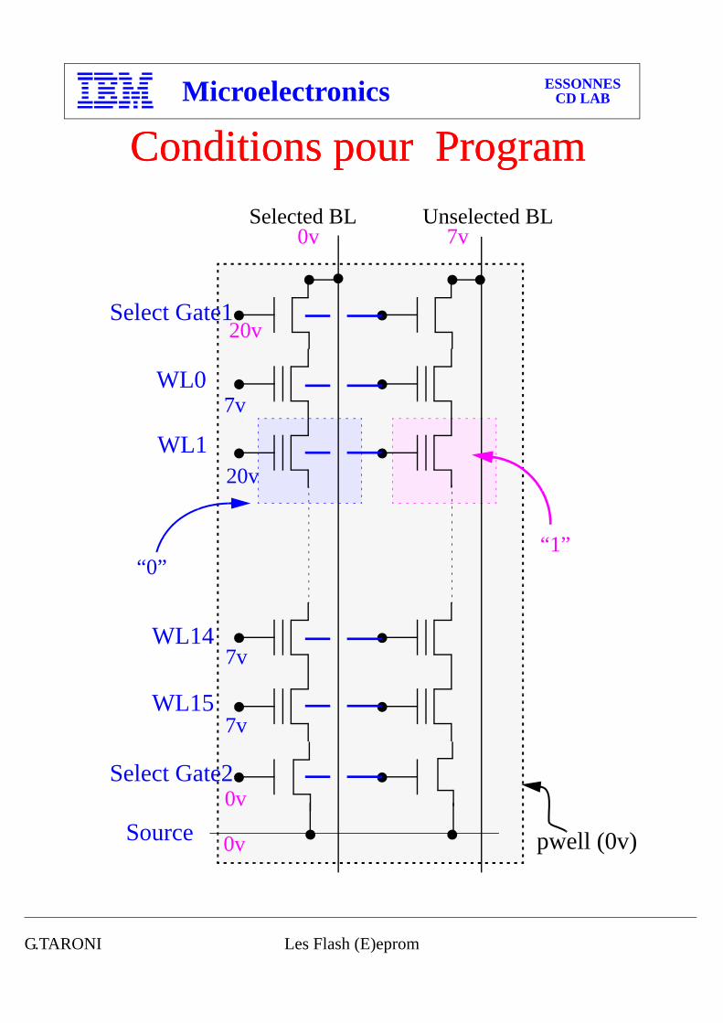
Conditions pour Program Conditions pour Program
WL0
WL1
WL15
WL14
Source
Select Gate2
Select Gate1
Selected BL Unselected BL
20v
0v 7v
7v
7v
7v
0v
0v
20v
pwell (0v)
“0”“1”
G.TARONI Les Flash (E)eprom
Microelectronics ESSONNESCD LAB
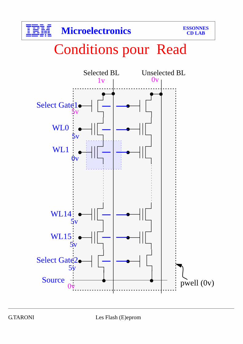
WL0
WL1
WL15
WL14
Source
Select Gate2
Select Gate1
Selected BL Unselected BL
Conditions pour Read
1v 0v
5v
5v
5v
5v
5v
0v
0v
pwell (0v)
G.TARONI Les Flash (E)eprom
Microelectronics ESSONNESCD LAB
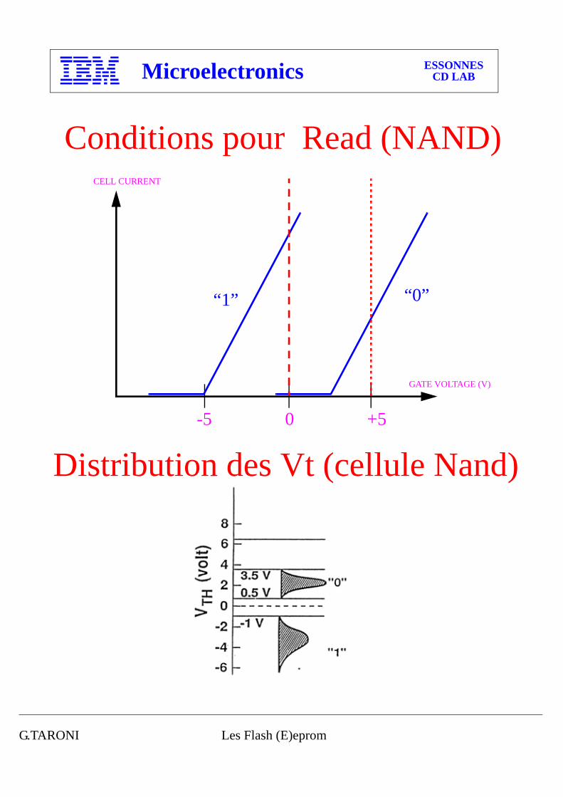
Conditions pour Read (NAND)
GATE VOLTAGE (V)
CELL CURRENT
“1” “0”
0-5 +5
Distribution des Vt (cellule Nand)
G.TARONI Les Flash (E)eprom
Microelectronics ESSONNESCD LAB
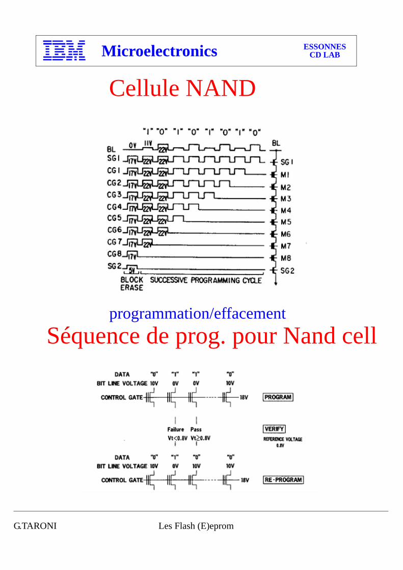
Cellule NAND
programmation/effacementSéquence de prog. pour Nand cell
G.TARONI Les Flash (E)eprom
Microelectronics ESSONNESCD LAB
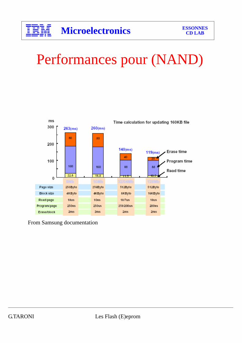
Performances pour (NAND)
From Samsung documentation
G.TARONI Les Flash (E)eprom
Microelectronics ESSONNESCD LAB
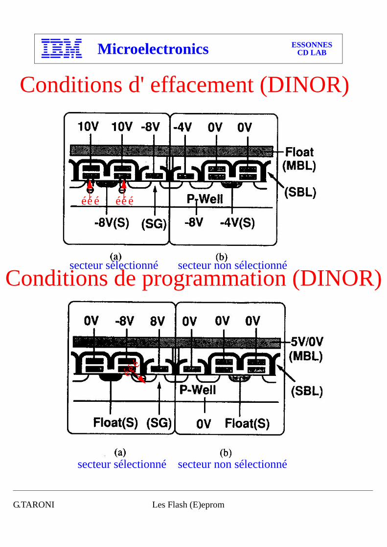
Conditions d' effacement (DINOR)
Conditions de programmation (DINOR)secteur sélectionné secteur non sélectionné
secteur non sélectionnésecteur sélectionné
éé é éé é
ééé
G.TARONI Les Flash (E)eprom
Microelectronics ESSONNESCD LAB
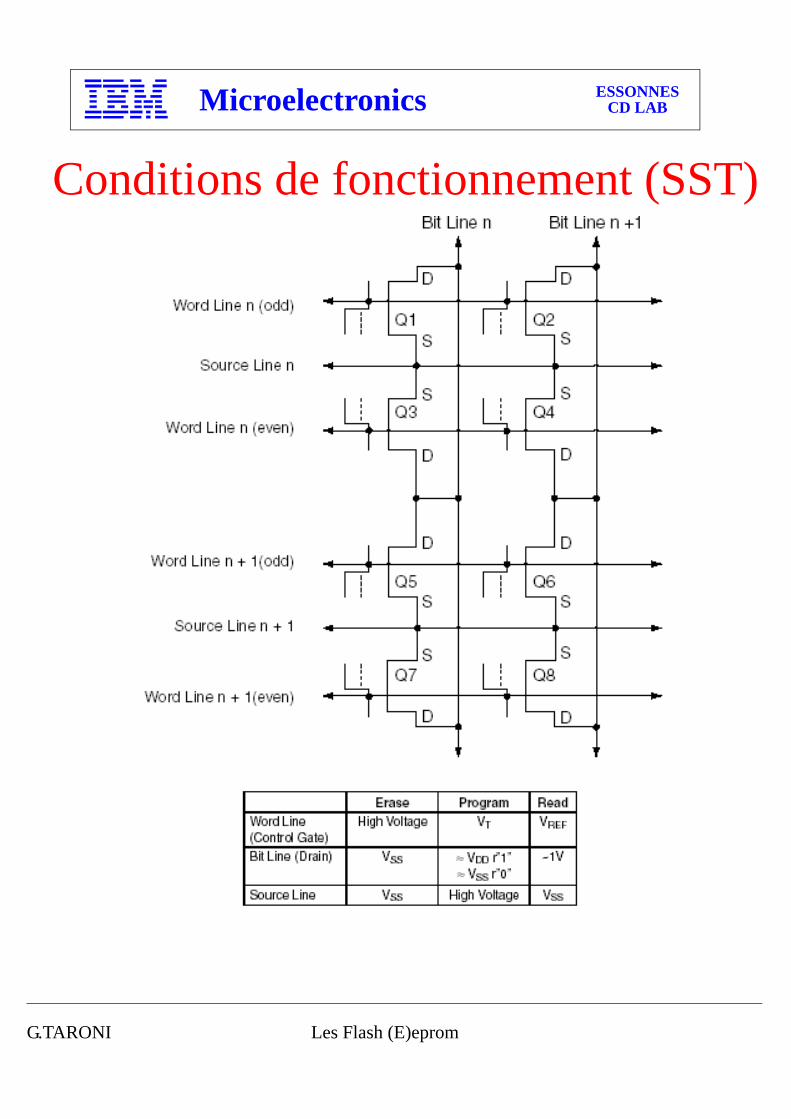
Conditions de fonctionnement (SST)
G.TARONI Les Flash (E)eprom
Microelectronics ESSONNESCD LAB
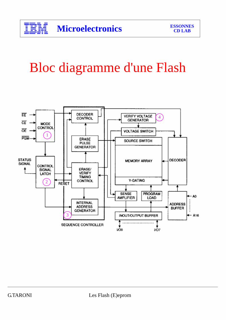
Bloc diagramme d'une Flash
1
2
3
4
G.TARONI Les Flash (E)eprom
Microelectronics ESSONNESCD LAB
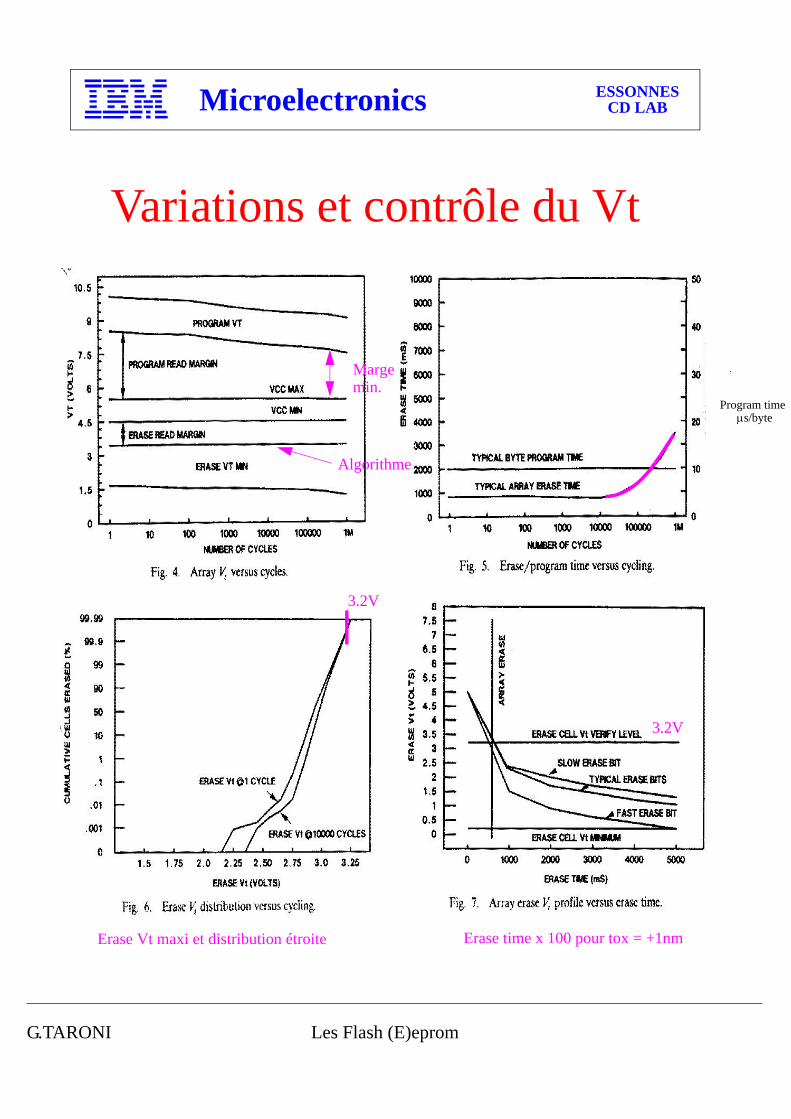
Variations et contrôle du Vt
Algorithme
3.2V
3.2V
µs/byteProgram time
Erase Vt maxi et distribution étroite
Margemin.
Erase time x 100 pour tox = +1nm
G.TARONI Les Flash (E)eprom
Microelectronics ESSONNESCD LAB
G.TARONI Les Flash (E)eprom
Microelectronics ESSONNESCD LAB
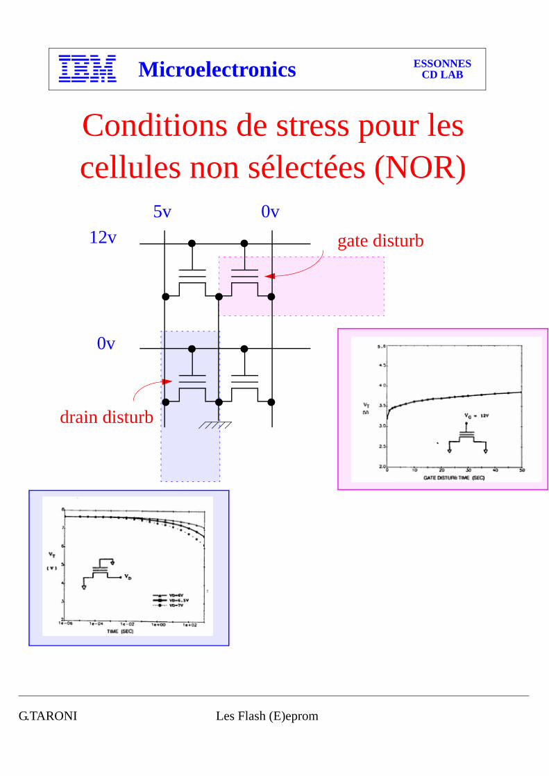
12v
0v
5v 0v
Conditions de stress pour les cellules non sélectées (NOR)
gate disturb
drain disturb
G.TARONI Les Flash (E)eprom
Microelectronics ESSONNESCD LAB
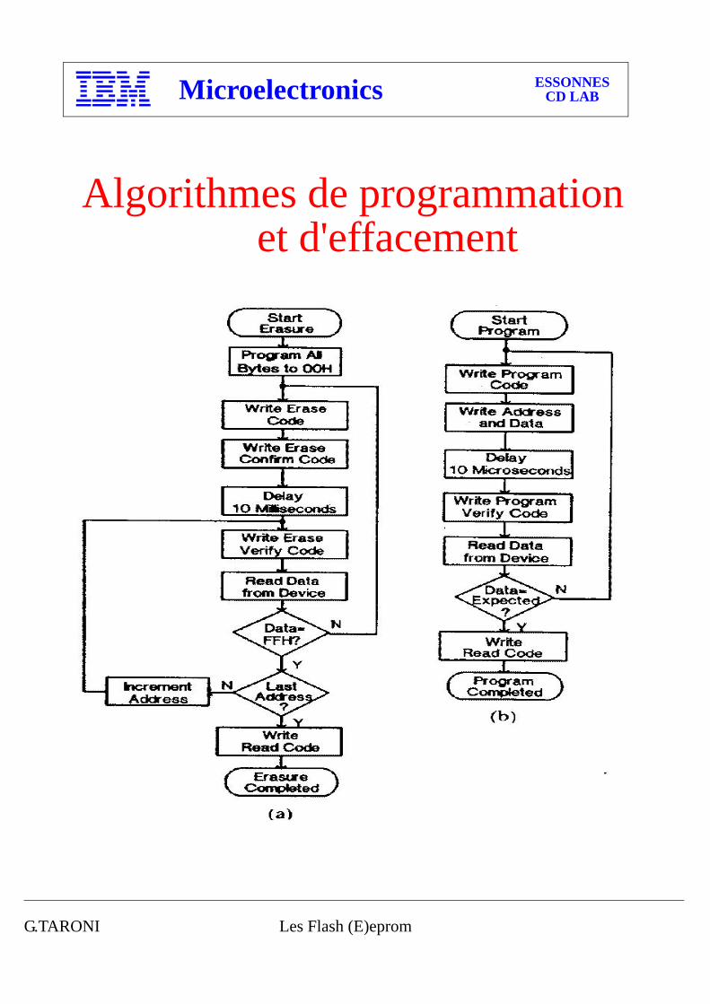
Algorithmes de programmationet d'effacement
G.TARONI Les Flash (E)eprom
Microelectronics ESSONNESCD LAB
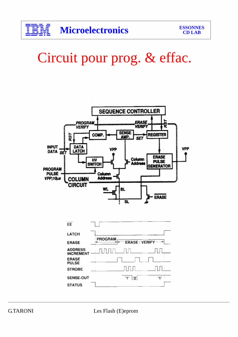
Circuit pour prog. & effac.
G.TARONI Les Flash (E)eprom
Microelectronics ESSONNESCD LAB
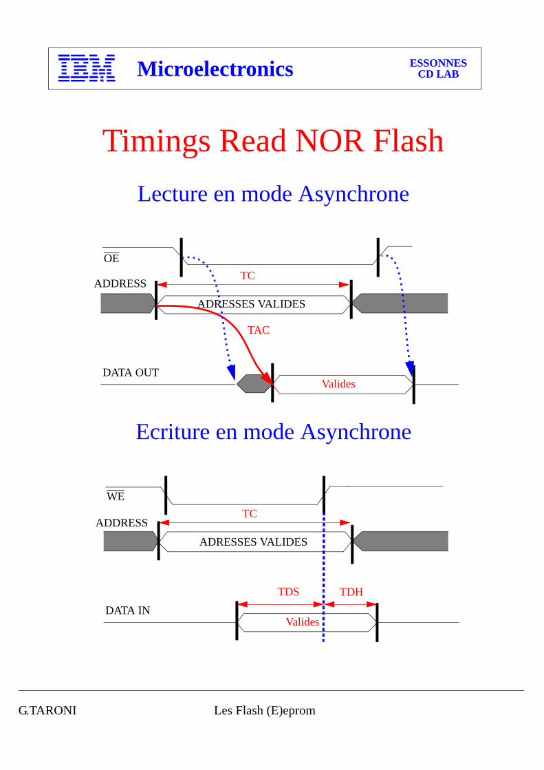
Timings Read NOR Flash
OE
ADRESSES VALIDES
DATA OUT Valides
Lecture en mode Asynchrone
TC
TAC
ADDRESS
WE
ADRESSES VALIDES
DATA IN Valides
Ecriture en mode Asynchrone
TDS TDH
TCADDRESS
G.TARONI Les Flash (E)eprom
Microelectronics ESSONNESCD LAB
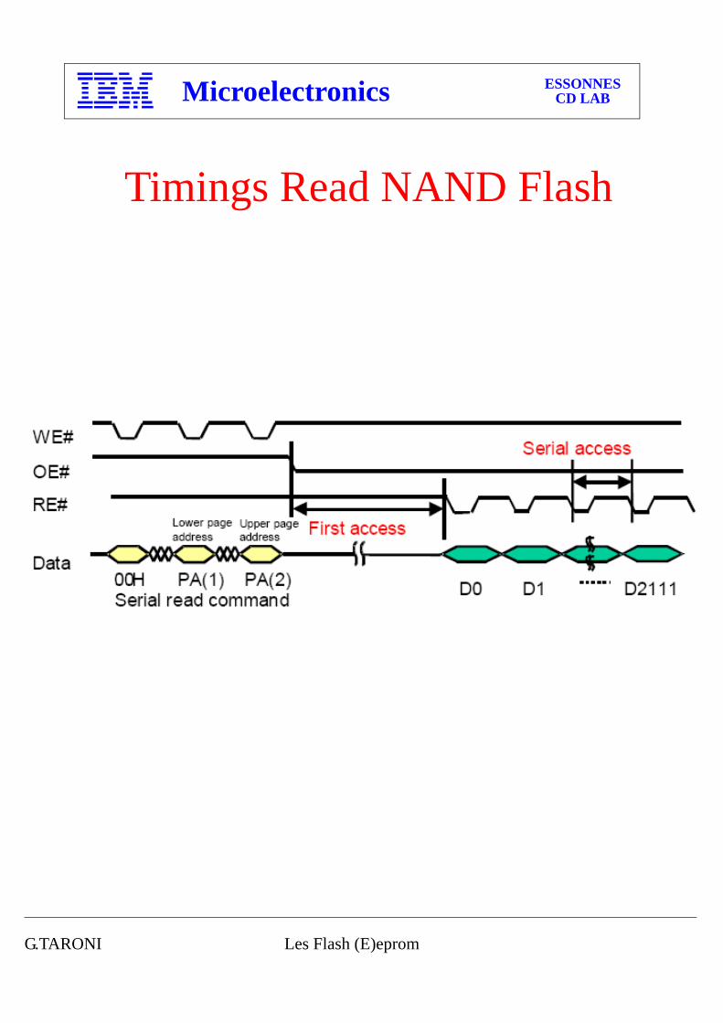
Timings Read NAND Flash
G.TARONI Les Flash (E)eprom
Microelectronics ESSONNESCD LAB
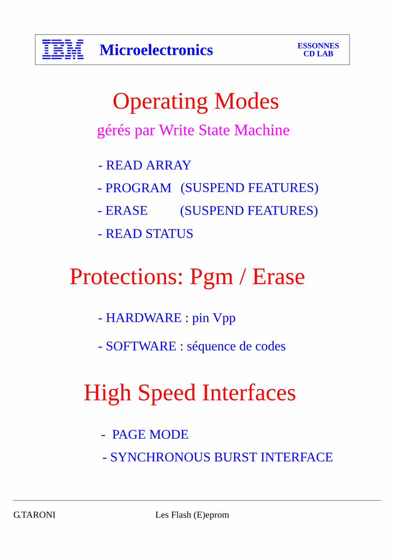
Operating Modes
- READ ARRAY
- PROGRAM
- ERASE
- READ STATUS
Protections: Pgm / Erase - HARDWARE : pin Vpp
- SOFTWARE : séquence de codes
(SUSPEND FEATURES)
(SUSPEND FEATURES)
gérés par Write State Machine
High Speed Interfaces- PAGE MODE
- SYNCHRONOUS BURST INTERFACE
G.TARONI Les Flash (E)eprom
Microelectronics ESSONNESCD LAB
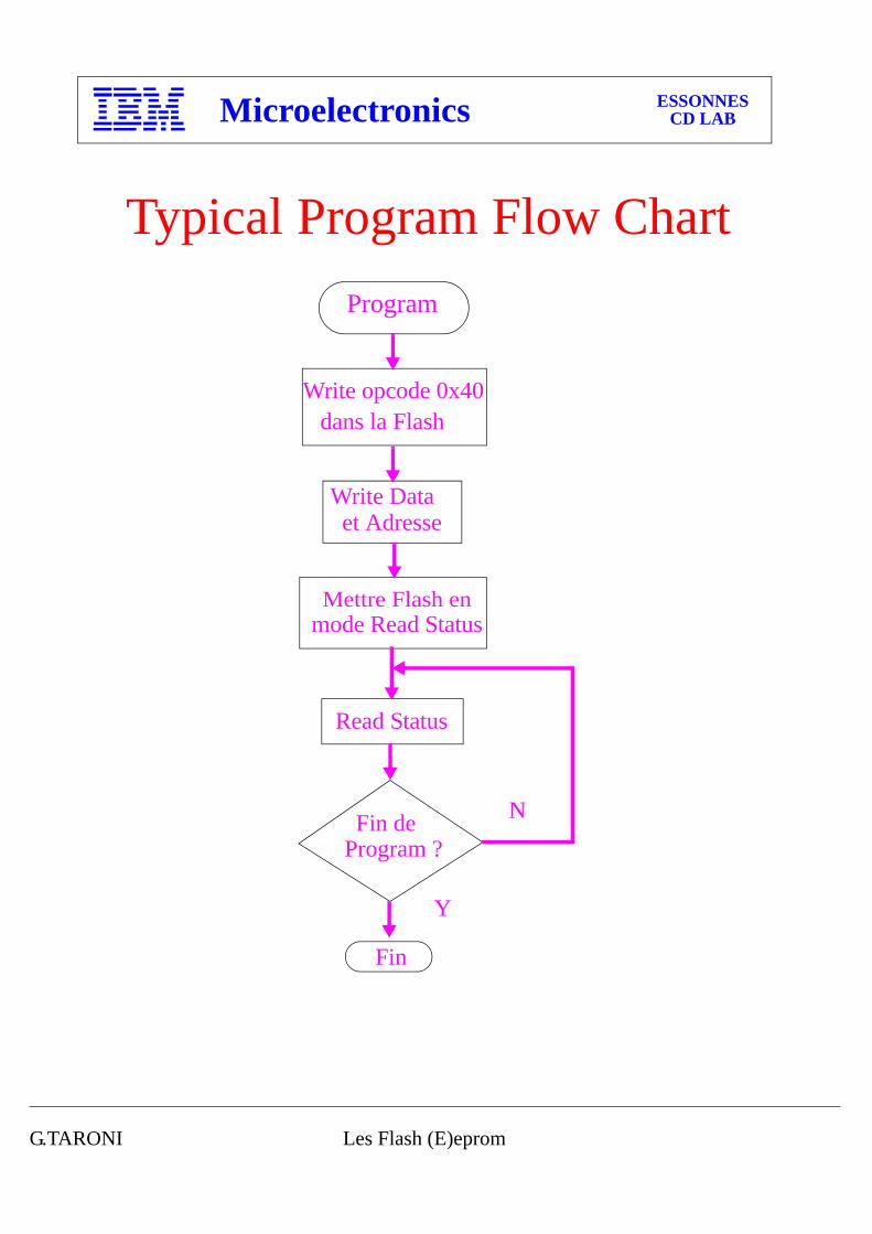
Program
Write opcode 0x40dans la Flash
Write Data et Adresse
Mettre Flash enmode Read Status
Read Status
Fin
Program ?Fin de
Y
N
Typical Program Flow Chart
G.TARONI Les Flash (E)eprom
Microelectronics ESSONNESCD LAB
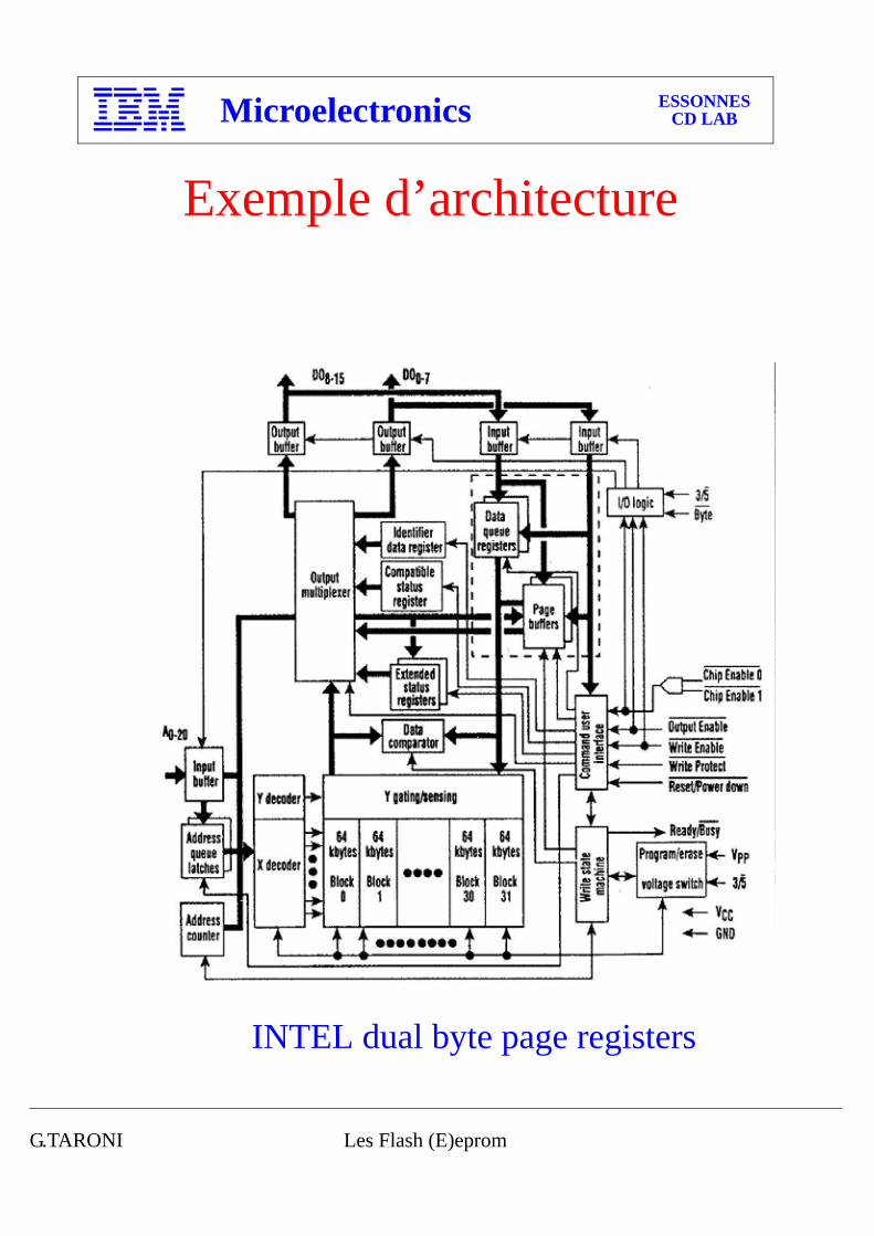
INTEL dual byte page registers
Exemple d’architecture
G.TARONI Les Flash (E)eprom
Microelectronics ESSONNESCD LAB
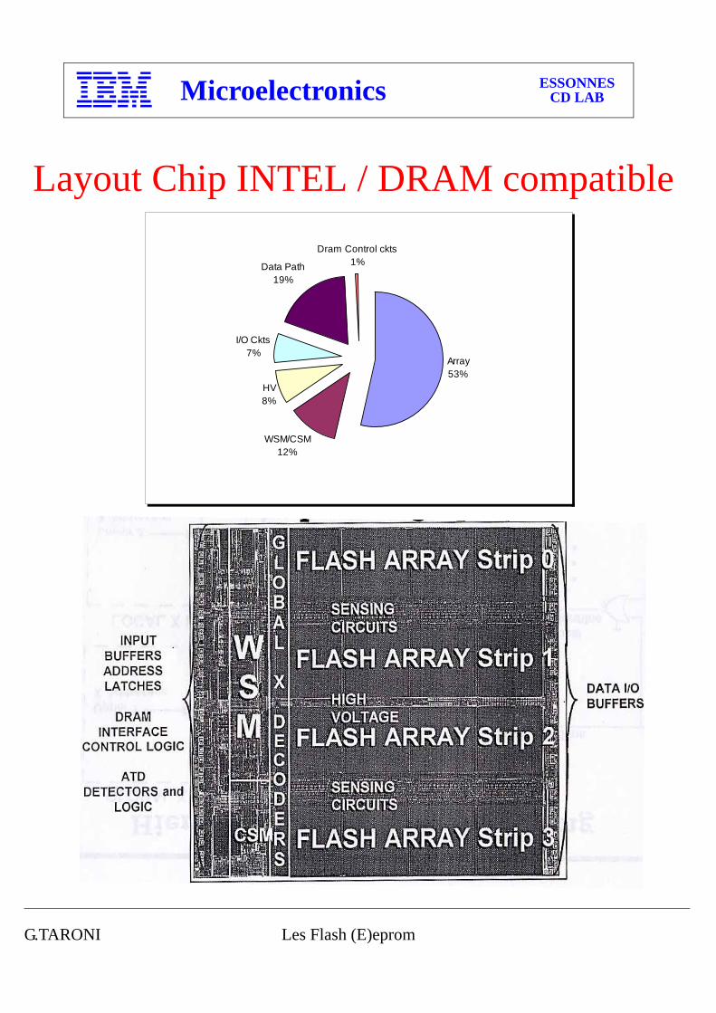
Layout Chip INTEL / DRAM compatible
Array53%
WSM/CSM12%
HV8%
I/O Ckts7%
Data Path19%
Dram Control ckts1%
G.TARONI Les Flash (E)eprom
Microelectronics ESSONNESCD LAB
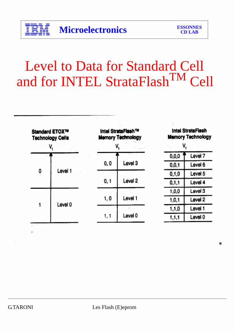
Level to Data for Standard Cell and for INTEL StrataFlashTM Cell
G.TARONI Les Flash (E)eprom
Microelectronics ESSONNESCD LAB
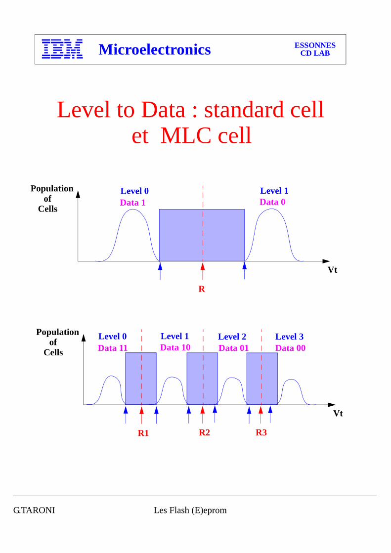
Level to Data : standard cell et MLC cell
Vt
Population of
Cells
Level 0 Level 1
R
Data 0Data 1
Vt
Population of
Cells
Level 0 Level 1 Level 2 Level 3
R1 R2 R3
Data 00Data 01Data 10Data 11
G.TARONI Les Flash (E)eprom
Microelectronics ESSONNESCD LAB
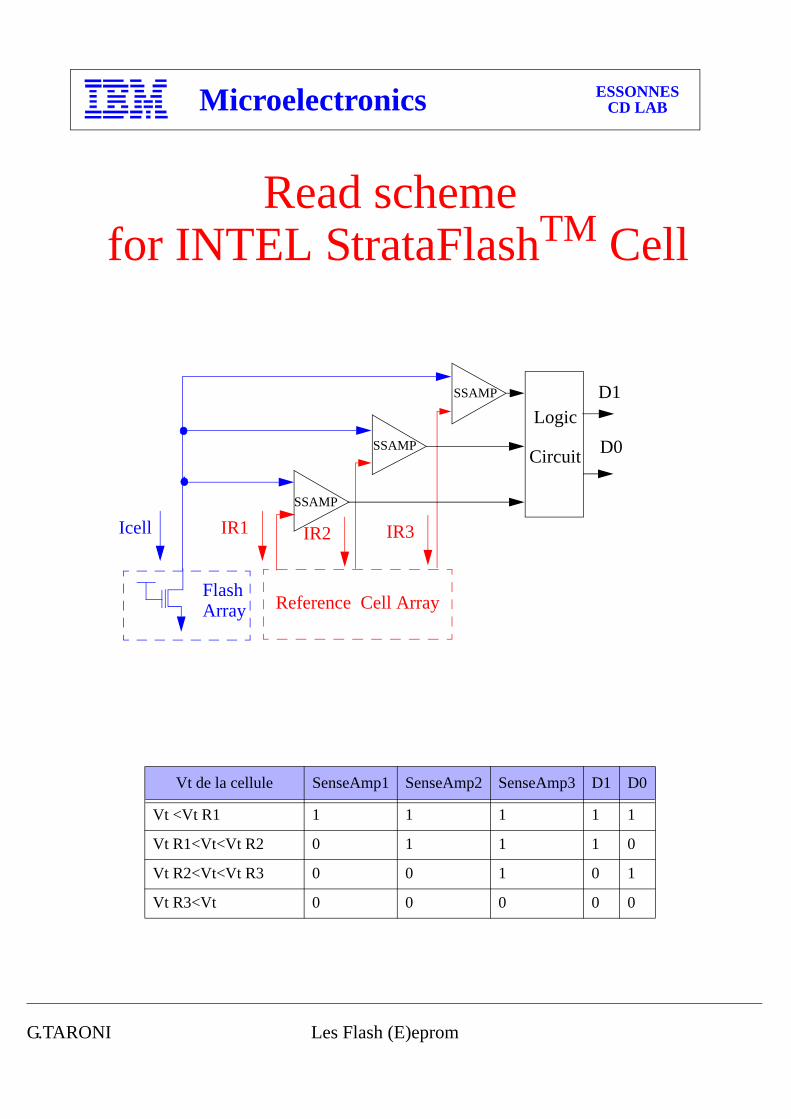
Read scheme for INTEL StrataFlashTM Cell
Vt de la cellule SenseAmp1 SenseAmp2 SenseAmp3 D1 D0
Vt <Vt R1 1 1 1 1 1
Vt R1<Vt<Vt R2 0 1 1 1 0
Vt R2<Vt<Vt R3 0 0 1 0 1
Vt R3<Vt 0 0 0 0 0
D1
D0Logic
Circuit
Reference Cell ArrayFlash Array
Icell IR1 IR2 IR3
SSAMP
SSAMP
SSAMP
G.TARONI Les Flash (E)eprom
Microelectronics ESSONNESCD LAB
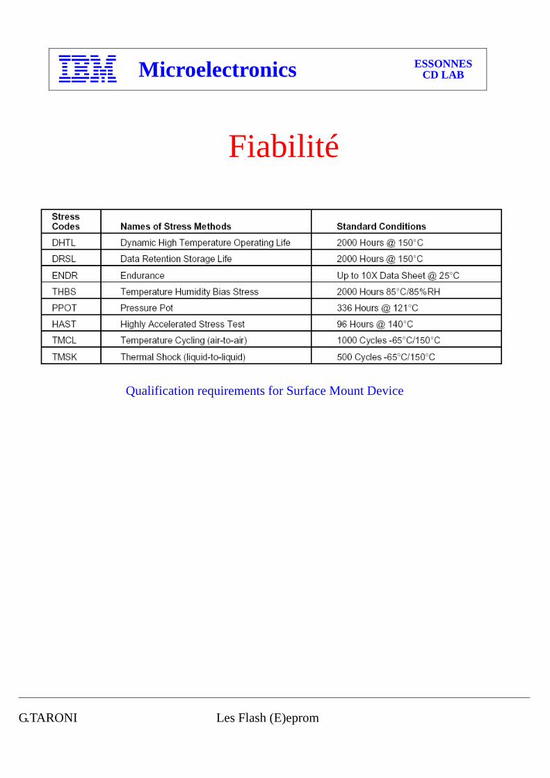
Fiabilité
Qualification requirements for Surface Mount Device
G.TARONI Les Flash (E)eprom
Microelectronics ESSONNESCD LAB
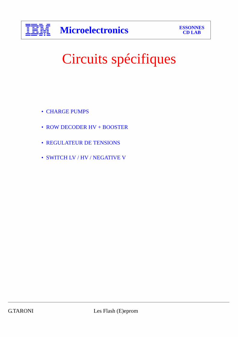
• CHARGE PUMPS
• ROW DECODER HV + BOOSTER
• REGULATEUR DE TENSIONS
• SWITCH LV / HV / NEGATIVE V
Circuits spécifiques
G.TARONI Les Flash (E)eprom
Microelectronics ESSONNESCD LAB
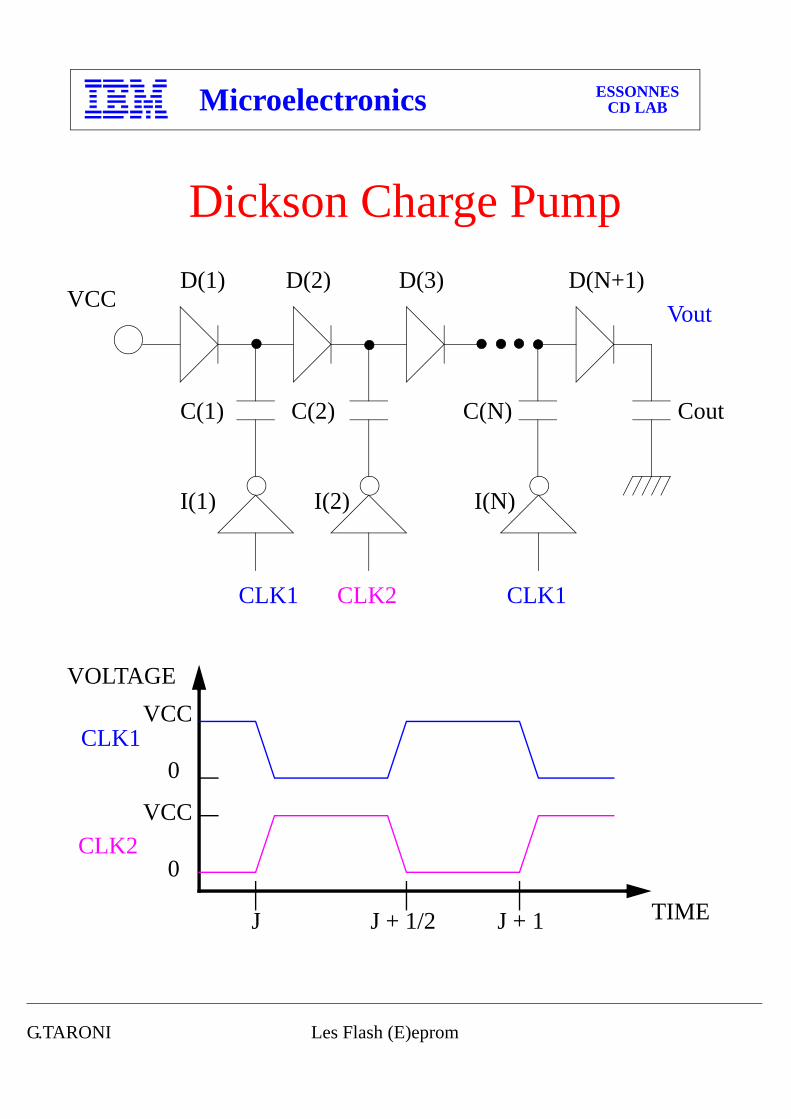
Dickson Charge Pump
VCCD(1) D(2) D(3) D(N+1)
C(N)C(1) C(2) Cout
I(1) I(2) I(N)
CLK1 CLK2 CLK1
J J + 1/2 J + 1 TIME
VOLTAGE
CLK1
CLK2
0
VCC
0
VCC
Vout
G.TARONI Les Flash (E)eprom
Microelectronics ESSONNESCD LAB
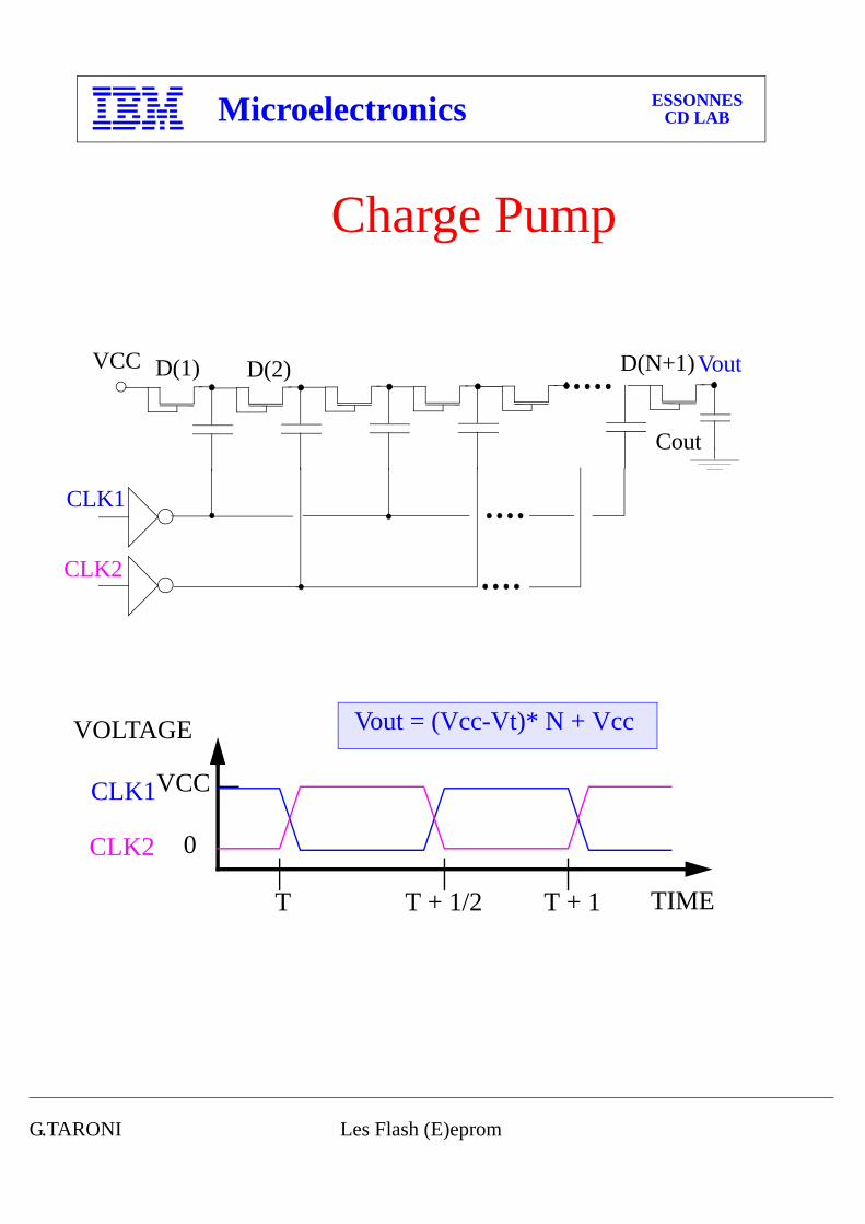
Charge Pump
VCC D(1) D(2) D(N+1)
Cout
CLK1
CLK2
T T + 1/2 T + 1 TIME
VOLTAGE
CLK1
CLK2 0
VCC
Vout = (Vcc-Vt)* N + Vcc
Vout
G.TARONI Les Flash (E)eprom
Microelectronics ESSONNESCD LAB
Performances NOR vs NAND
From Samsung documentation
G.TARONI Les Flash (E)eprom
Microelectronics ESSONNESCD LAB
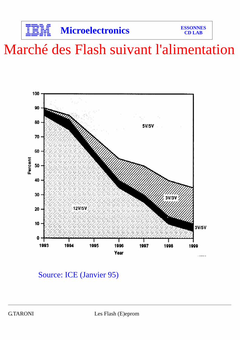
Source: ICE (Janvier 95)
Marché des Flash suivant l'alimentation
G.TARONI Les Flash (E)eprom
Microelectronics ESSONNESCD LAB
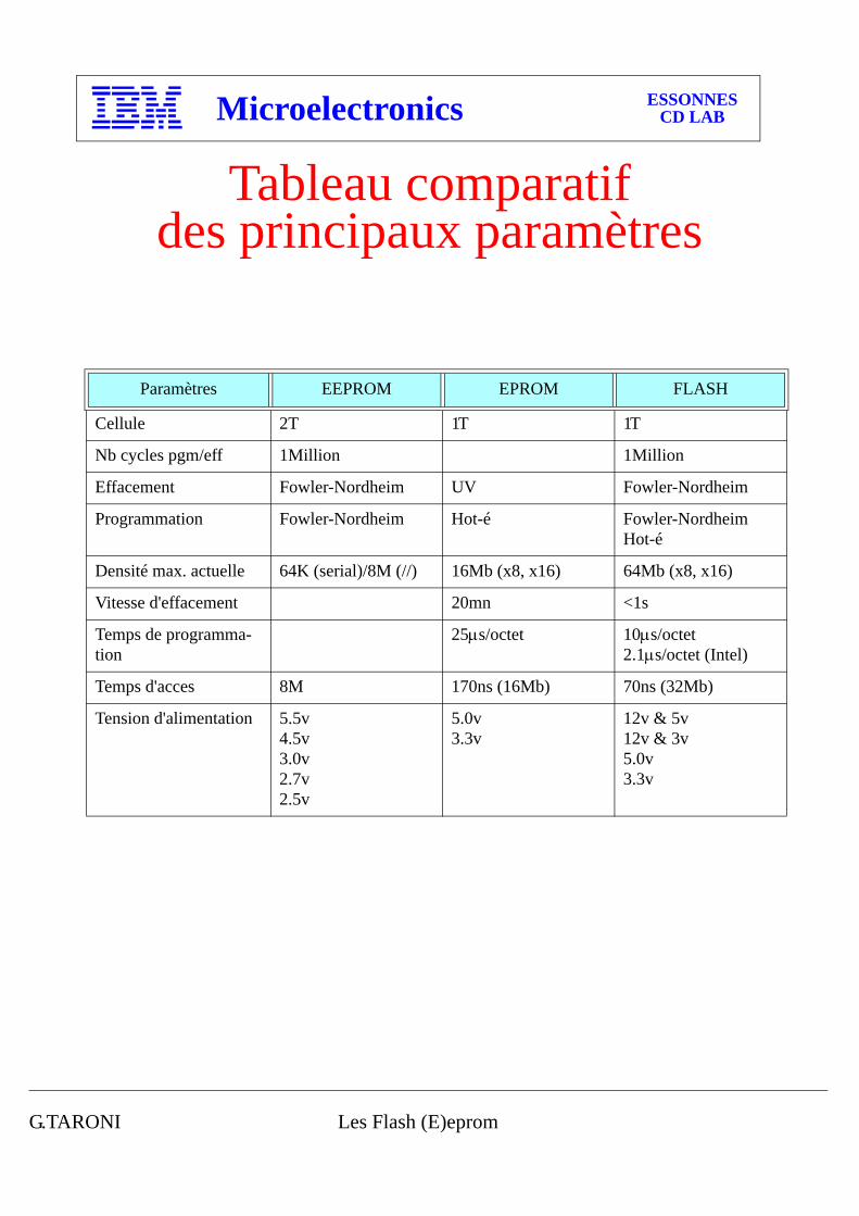
Paramètres EEPROM EPROM FLASH
Cellule 2T 1T 1T
Nb cycles pgm/eff 1Million 1Million
Effacement Fowler-Nordheim UV Fowler-Nordheim
Programmation Fowler-Nordheim Hot-é Fowler-NordheimHot-é
Densité max. actuelle 64K (serial)/8M (//) 16Mb (x8, x16) 64Mb (x8, x16)
Vitesse d'effacement 20mn <1s
Temps de programma-tion
25µs/octet 10µs/octet2.1µs/octet (Intel)
Temps d'acces 8M 170ns (16Mb) 70ns (32Mb)
Tension d'alimentation 5.5v4.5v3.0v2.7v2.5v
5.0v3.3v
12v & 5v12v & 3v5.0v3.3v
Tableau comparatifdes principaux paramètres
G.TARONI Les Flash (E)eprom
Microelectronics ESSONNESCD LAB
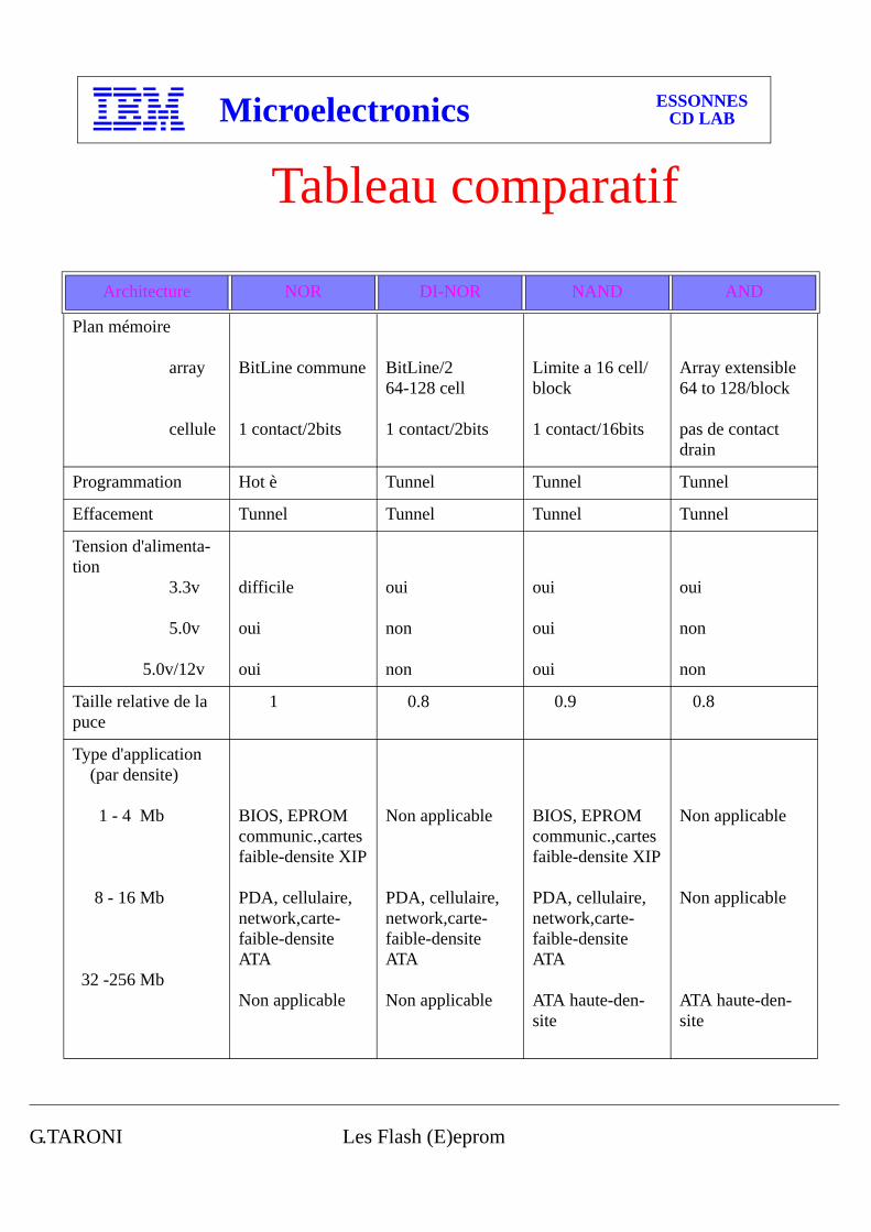
Architecture NOR DI-NOR NAND AND
Plan mémoire
array
cellule
BitLine commune
1 contact/2bits
BitLine/264-128 cell
1 contact/2bits
Limite a 16 cell/block
1 contact/16bits
Array extensible64 to 128/block
pas de contact drain
Programmation Hot è Tunnel Tunnel Tunnel
Effacement Tunnel Tunnel Tunnel Tunnel
Tension d'alimenta-tion 3.3v
5.0v
5.0v/12v
difficile
oui
oui
oui
non
non
oui
oui
oui
oui
non
non
Taille relative de la puce
1 0.8 0.9 0.8
Type d'application (par densite)
1 - 4 Mb
8 - 16 Mb
32 -256 Mb
BIOS, EPROMcommunic.,cartesfaible-densite XIP
PDA, cellulaire, network,carte-faible-densite ATA
Non applicable
Non applicable
PDA, cellulaire, network,carte-faible-densite ATA
Non applicable
BIOS, EPROMcommunic.,cartesfaible-densite XIP
PDA, cellulaire, network,carte-faible-densite ATA
ATA haute-den-site
Non applicable
Non applicable
ATA haute-den-site
Tableau comparatif
G.TARONI Les Flash (E)eprom
Microelectronics ESSONNESCD LAB
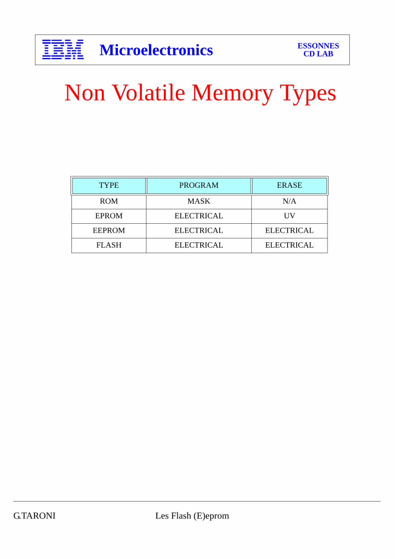
Non Volatile Memory Types
TYPE PROGRAM ERASE
ROM MASK N/A
EPROM ELECTRICAL UV
EEPROM ELECTRICAL ELECTRICAL
FLASH ELECTRICAL ELECTRICAL
G.TARONI Les Flash (E)eprom
Microelectronics ESSONNESCD LAB
Flash par type de stockage
Program / Code storage Data storage
Program Configuration Personalization Recorded
CD-ROM drive 3 3
Cellular phone 3 3 3
Data bank 3 3 3
Digital camera 3 3 3
Hard disk drive 3 3
Instrumentation 3 3 3
Memory card 3 3 3
Modem 3 3
Networking 3 3
Operating system 3 3 3
Point of sales 3 3
Voice recorder 3 3
G.TARONI Les Mémoires Associatives
Microelectronics ESSONNESCD LAB
Les Mémoires associatives
G.TARONI Les Mémoires Associatives
Microelectronics ESSONNESCD LAB
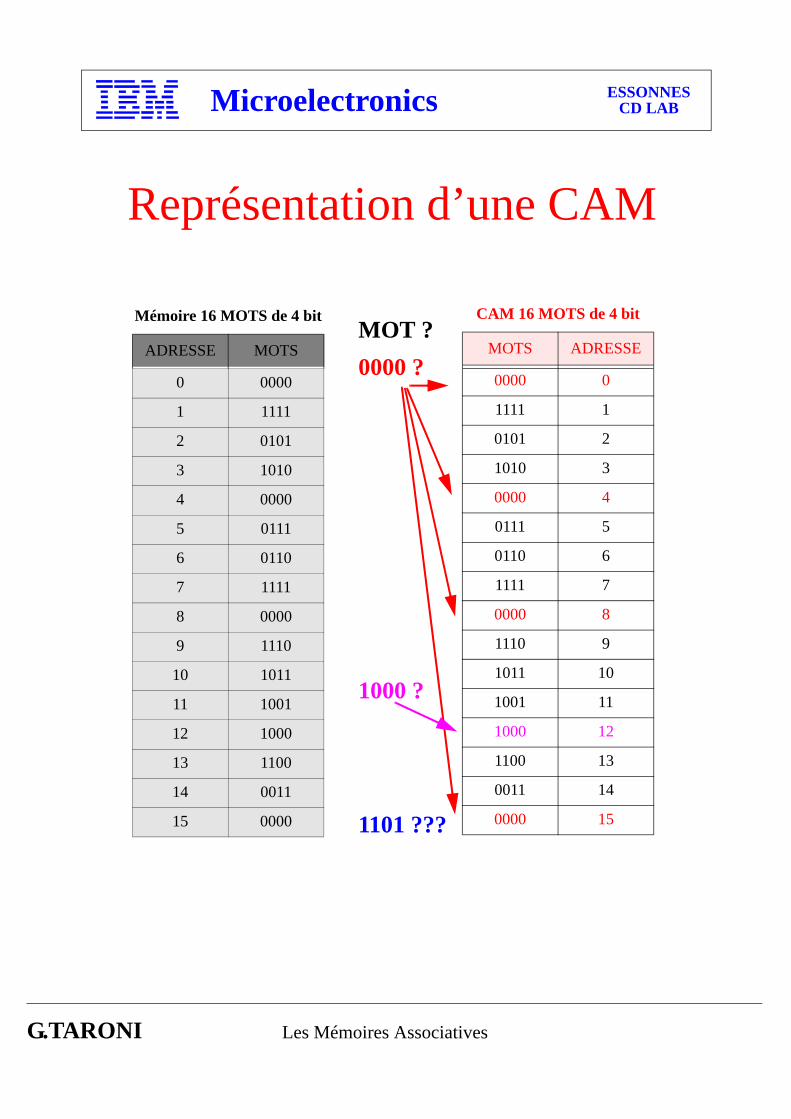
Représentation d’une CAM
Mémoire 16 MOTS de 4 bit
ADRESSE MOTS
0 0000
1 1111
2 0101
3 1010
4 0000
5 0111
6 0110
7 1111
8 0000
9 1110
10 1011
11 1001
12 1000
13 1100
14 0011
15 0000
CAM 16 MOTS de 4 bit
MOTS ADRESSE
0000 0
1111 1
0101 2
1010 3
0000 4
0111 5
0110 6
1111 7
0000 8
1110 9
1011 10
1001 11
1000 12
1100 13
0011 14
0000 15
0000 ?
1101 ???
1000 ?
MOT ?
G.TARONI Les Mémoires Associatives
Microelectronics ESSONNESCD LAB
Applications
- mémoires virtuelles
- cache pour disques magnétiques et optiques
- accélérateurs pour bases de données
- compression de données
- processeur d'images
- LAN (bridges, routers, switches ATM)
G.TARONI Les Mémoires Associatives
Microelectronics ESSONNESCD LAB
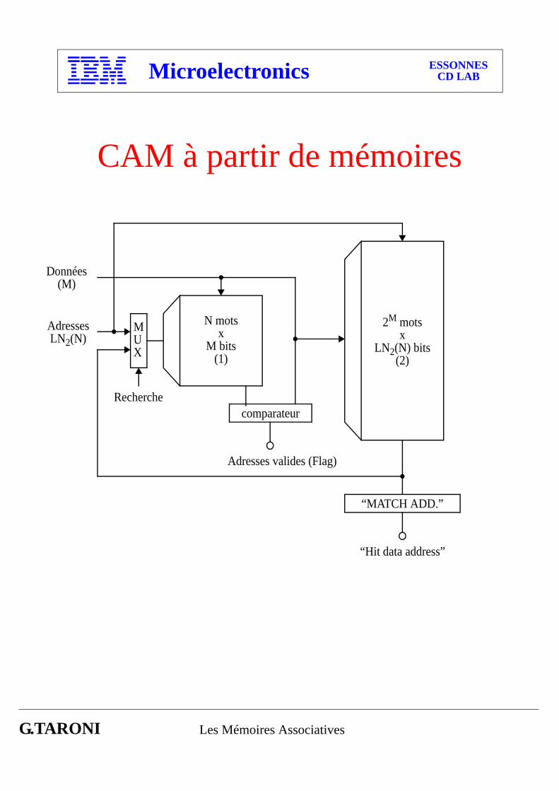
N motsx
M bits(1)
comparateur
2M motsx
LN2(N) bits(2)
MUX
“MATCH ADD.”
Recherche
“Hit data address”
Adresses valides (Flag)
Données(M)
AdressesLN2(N)
CAM à partir de mémoires
G.TARONI Les Mémoires Associatives
Microelectronics ESSONNESCD LAB
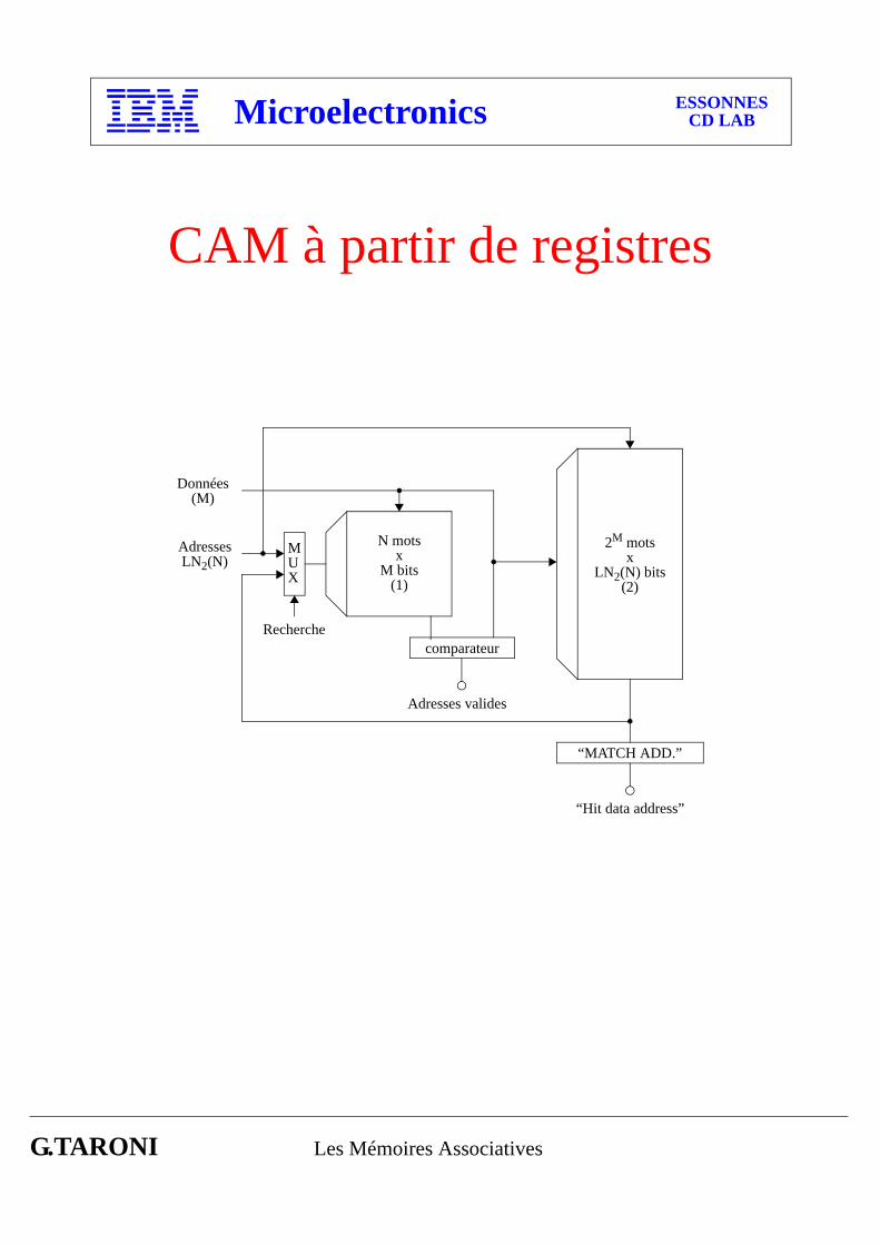
CAM à partir de registres
N motsx
M bits(1)
comparateur
2M motsx
LN2(N) bits(2)
MUX
“MATCH ADD.”
Recherche
“Hit data address”
Adresses valides
Données(M)
AdressesLN2(N)
G.TARONI Les Mémoires Associatives
Microelectronics ESSONNESCD LAB
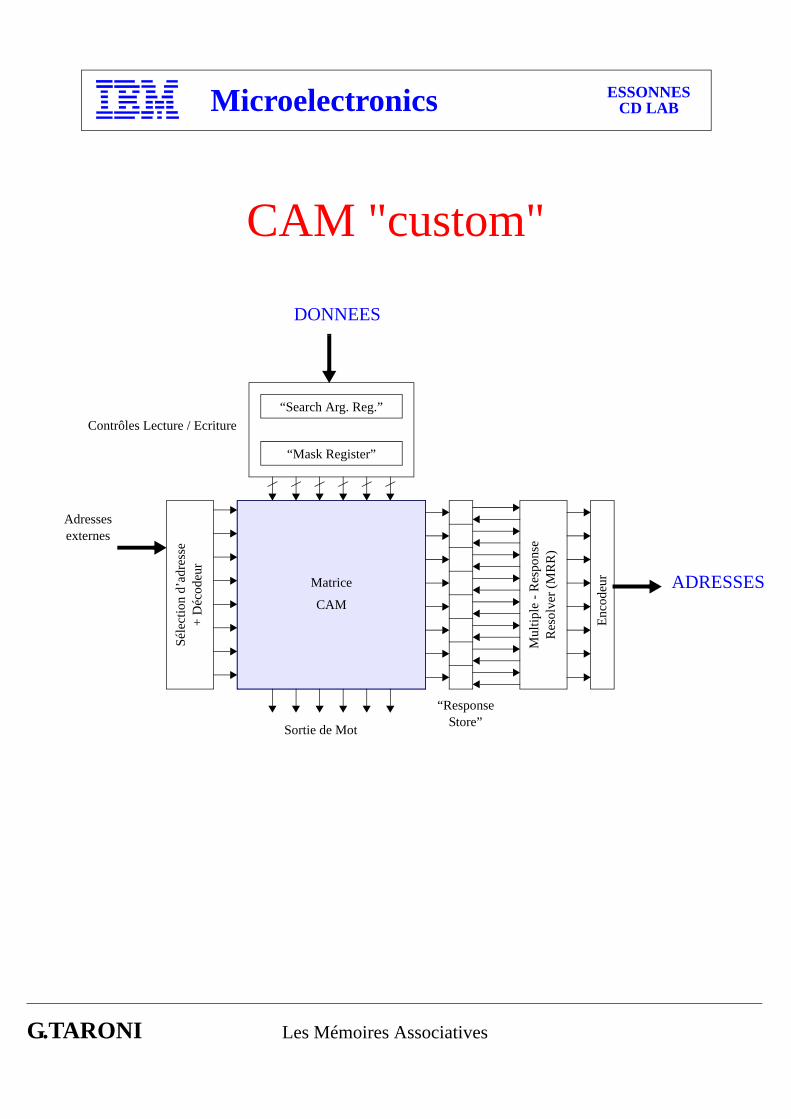
CAM "custom"
“Search Arg. Reg.”
“Mask Register”
Contrôles Lecture / Ecriture
Matrice
CAM
Mul
tiple
- R
espo
nse
Res
olve
r (M
RR
)
Enco
deur
Sortie de Mot
Séle
ctio
n d’
adre
sse
+ D
écod
eur
“ResponseStore”
Adressesexternes
ADRESSES
DONNEES
G.TARONI Les Mémoires Associatives
Microelectronics ESSONNESCD LAB
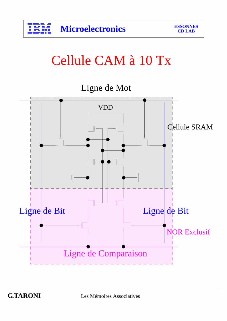
Ligne de Bit
Ligne de Mot
Ligne de Bit
VDD
Ligne de Comparaison
Cellule SRAM
NOR Exclusif
Cellule CAM à 10 Tx
G.TARONI Les Mémoires Associatives
Microelectronics ESSONNESCD LAB
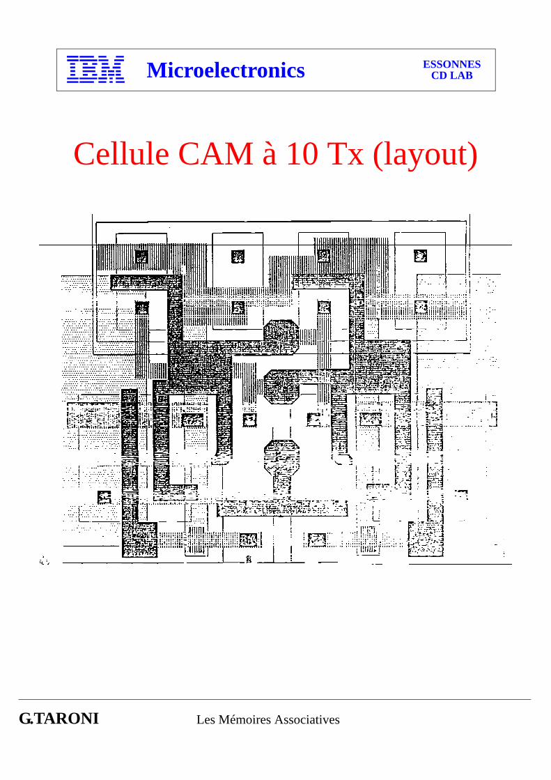
Cellule CAM à 10 Tx (layout)
G.TARONI Les Mémoires Associatives
Microelectronics ESSONNESCD LAB
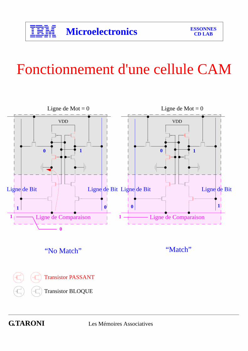
Ligne de Bit
Ligne de Mot = 0
Ligne de Bit
VDD
Ligne de Comparaison
Ligne de Bit
Ligne de Mot = 0
Ligne de Bit
VDD
Ligne de Comparaison
“No Match” “Match”
1
0
0
1 0
0 1
1
Fonctionnement d'une cellule CAM
1 1
0
Transistor PASSANT
Transistor BLOQUE
G.TARONI Les Mémoires Associatives
Microelectronics ESSONNESCD LAB
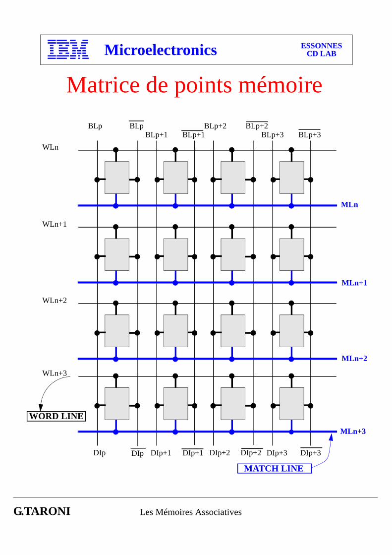
Matrice de points mémoire
WLn
BLpBLp+1
BLpBLp+1
BLp+2BLp+3
BLp+2BLp+3
WORD LINE
MATCH LINE
MLn
WLn+1
MLn+1
WLn+2
MLn+2
WLn+3
MLn+3
DIp DIp+1DIp DIp+1 DIp+2 DIp+3DIp+2 DIp+3
G.TARONI Les Mémoires Associatives
Microelectronics ESSONNESCD LAB
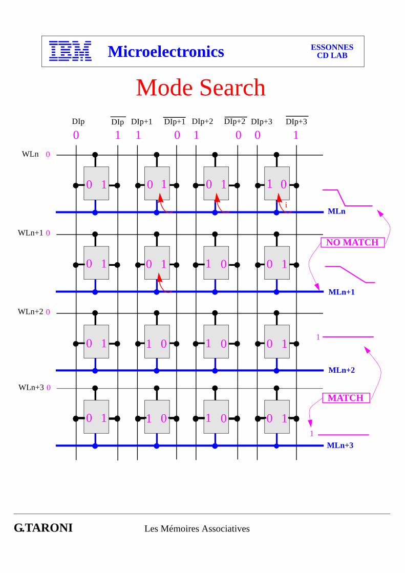
Mode Search
WLn
MATCH
MLn
WLn+1
MLn+1
WLn+2
MLn+2
WLn+3
MLn+3
DIp DIp+1DIp DIp+1 DIp+2 DIp+3DIp+2 DIp+3
0
0 0 0 1111
0 1 10 0 1 1 0i
0 1 1 0 0 1
0
0
0
0
0 1
01 1 0 0 10 1
01 1 0 0 10 1
NO MATCH
1
1
G.TARONI Les Mémoires Associatives
Microelectronics ESSONNESCD LAB
Ligne “Match”
Lignede mot
Ligne de bitgauche
Ligne de Bitdroite
VDD
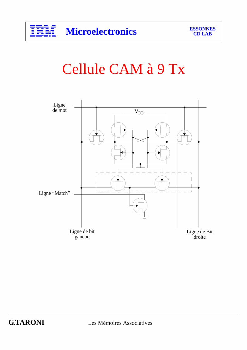
Cellule CAM à 9 Tx
G.TARONI Les Mémoires Associatives
Microelectronics ESSONNESCD LAB
Ligne “Match”
Lignede mot
Ligne de bitgauche
Ligne de Bitdroite
VDD
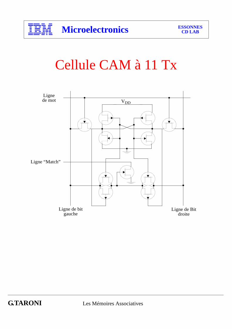
Cellule CAM à 11 Tx
G.TARONI Les Mémoires Associatives
Microelectronics ESSONNESCD LAB
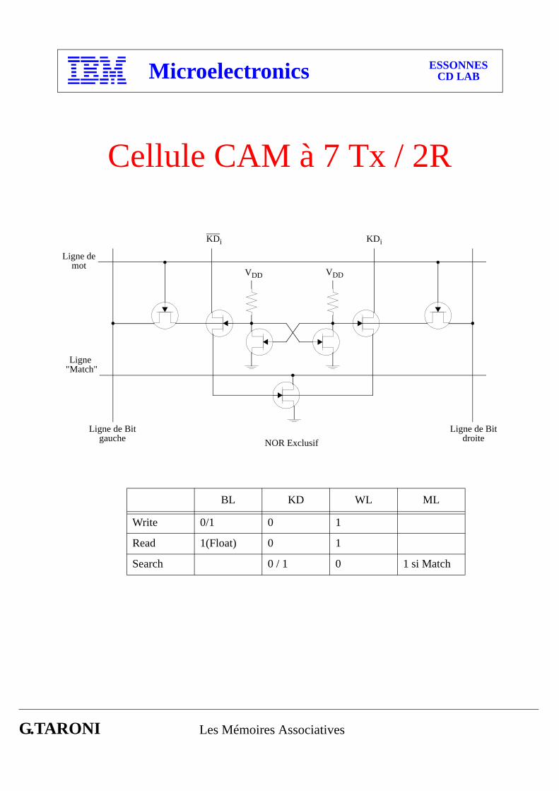
VDD VDD
NOR ExclusifLigne de Bit
droiteLigne de Bit
gauche
KDi KDi
Ligne demot
Ligne "Match"
Cellule CAM à 7 Tx / 2R
BL KD WL ML
Write 0/1 0 1
Read 1(Float) 0 1
Search 0 / 1 0 1 si Match
G.TARONI Les Mémoires Associatives
Microelectronics ESSONNESCD LAB
RW
DX
M0 M1
DY
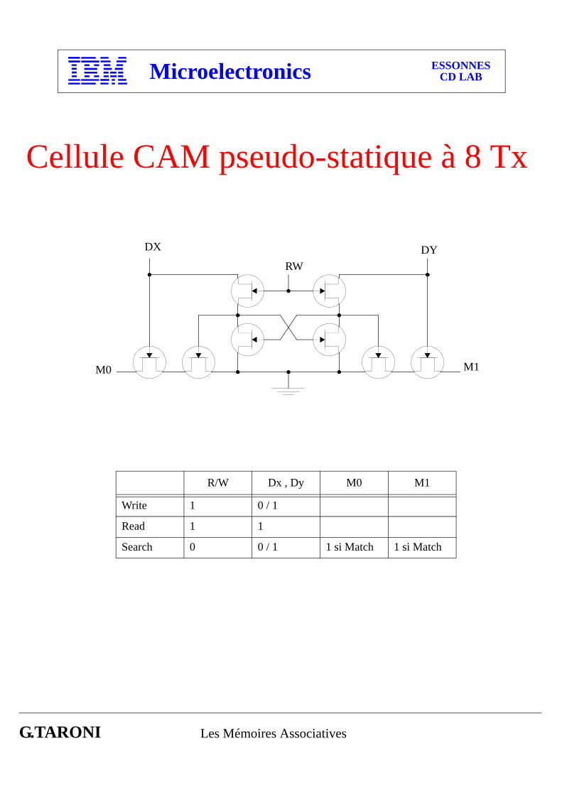
Cellule CAM pseudo-statique à 8 Tx
R/W Dx , Dy M0 M1
Write 1 0 / 1
Read 1 1
Search 0 0 / 1 1 si Match 1 si Match
G.TARONI Les Mémoires Associatives
Microelectronics ESSONNESCD LAB
Ligne de Mot
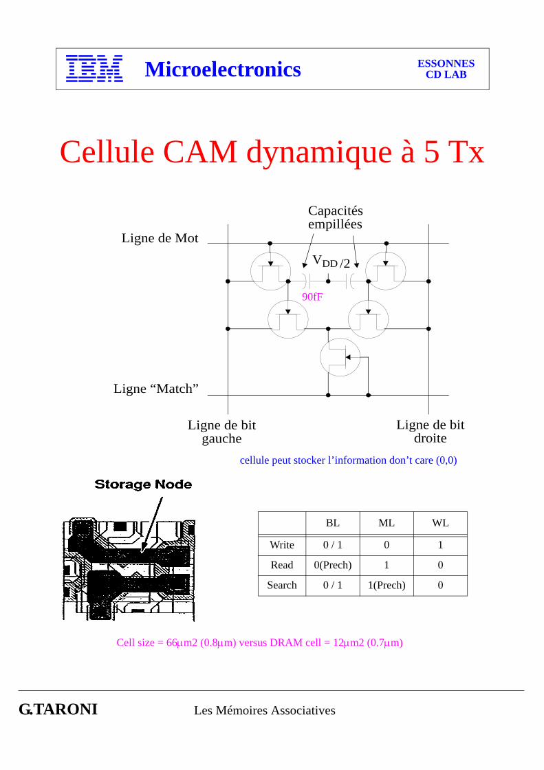
Capacitésempillées
Ligne “Match”
Ligne de bitgauche
Ligne de bitdroite
Cellule CAM dynamique à 5 Tx
90fF
BL ML WL
Write 0 / 1 0 1
Read 0(Prech) 1 0
Search 0 / 1 1(Prech) 0
Cell size = 66µm2 (0.8µm) versus DRAM cell = 12µm2 (0.7µm)
cellule peut stocker l’information don’t care (0,0)
VDD /2
G.TARONI Les Mémoires Associatives
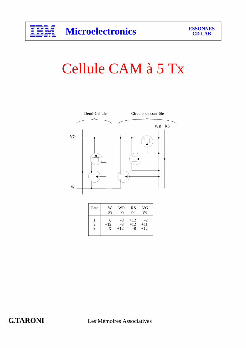
Microelectronics ESSONNESCD LAB
RSWR
VG
W
Demi-Cellule Circuits de contrôle
123
0+12
X
-8-8
+12
+12+12
-8
-2+11+12
Etat W(V)
WR(V)
RS(V)
VG(V)
Cellule CAM à 5 Tx
G.TARONI Les Mémoires Associatives
Microelectronics ESSONNESCD LAB
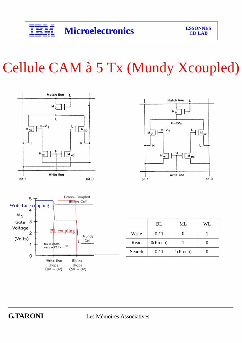
Cellule CAM à 5 Tx (Mundy Xcoupled)
BL ML WL
Write 0 / 1 0 1
Read 0(Prech) 1 0
Search 0 / 1 1(Prech) 0
Write Line coupling
BL coupling
G.TARONI Les Mémoires Associatives
Microelectronics ESSONNESCD LAB
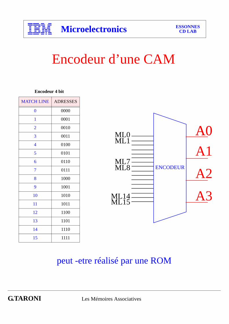
Encodeur d’une CAM
Encodeur 4 bit
MATCH LINE ADRESSES
0 0000
1 0001
2 0010
3 0011
4 0100
5 0101
6 0110
7 0111
8 1000
9 1001
10 1010
11 1011
12 1100
13 1101
14 1110
15 1111
peut -etre réalisé par une ROM
A0A0A1A2A3
ML0
ML14ML15
ML1
ML7ML8 ENCODEUR
G.TARONI Les Mémoires Associatives
Microelectronics ESSONNESCD LAB
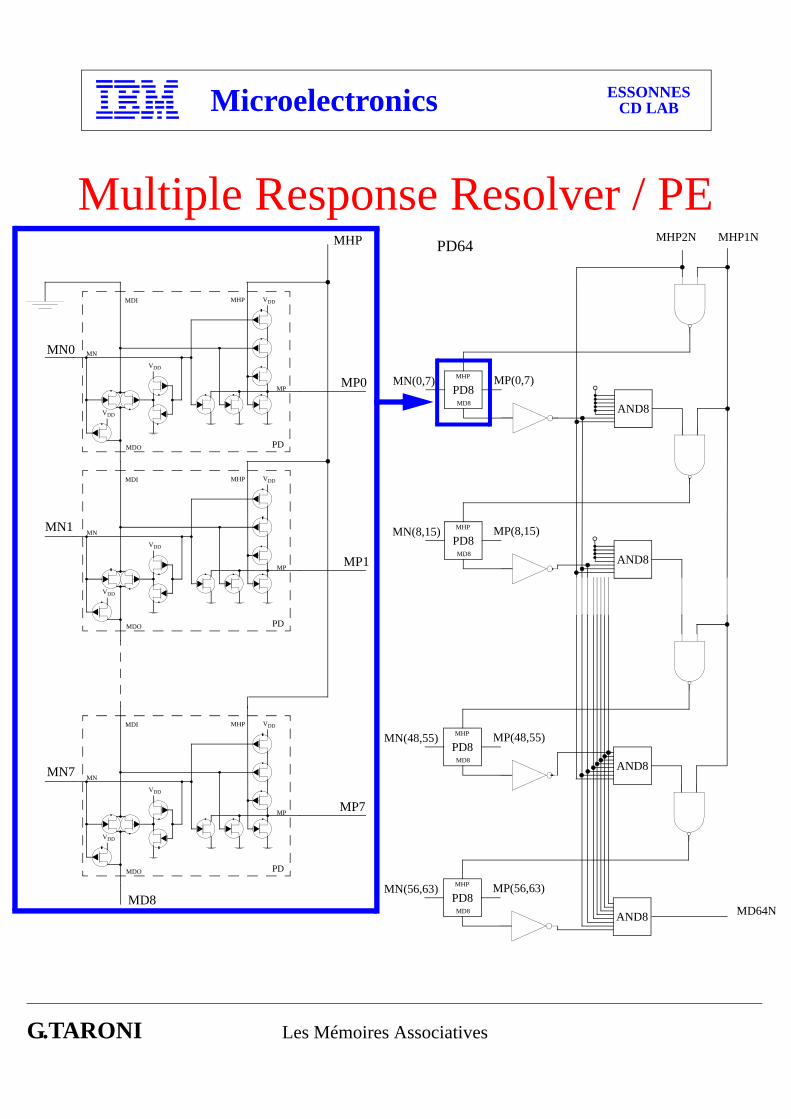
Multiple Response Resolver / PE
VDD
VDD
VDD
MP
PDMDO
MN
MDI MHP
VDD
VDD
VDD
MP
PDMDO
MN
MDI MHP
VDD
VDD
VDD
MP
PDMDO
MN
MDI MHP
MD8
MN7
MP7
MN1
MP1
MP0
MHP
MN0
AND8
MHP1NMHP2N
MP(0,7)MN(0,7)
AND8PD8
MP(8,15)MN(8,15)
MD8
MHP
PD8MD8
MHP
AND8
MP(48,55)MN(48,55)
AND8PD8
MP(56,63)MN(56,63)
MD8
MHP
PD8MD8
MHP
MD64N
PD64
G.TARONI Les Mémoires Associatives
Microelectronics ESSONNESCD LAB
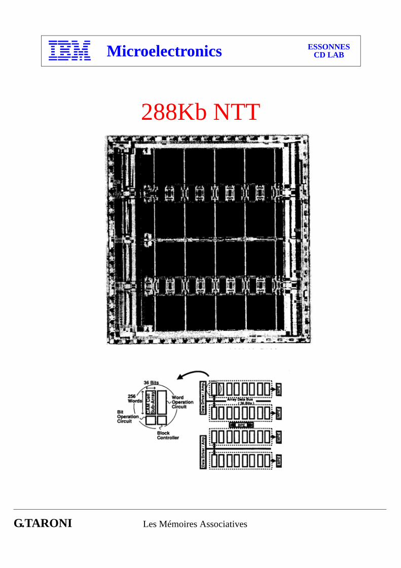
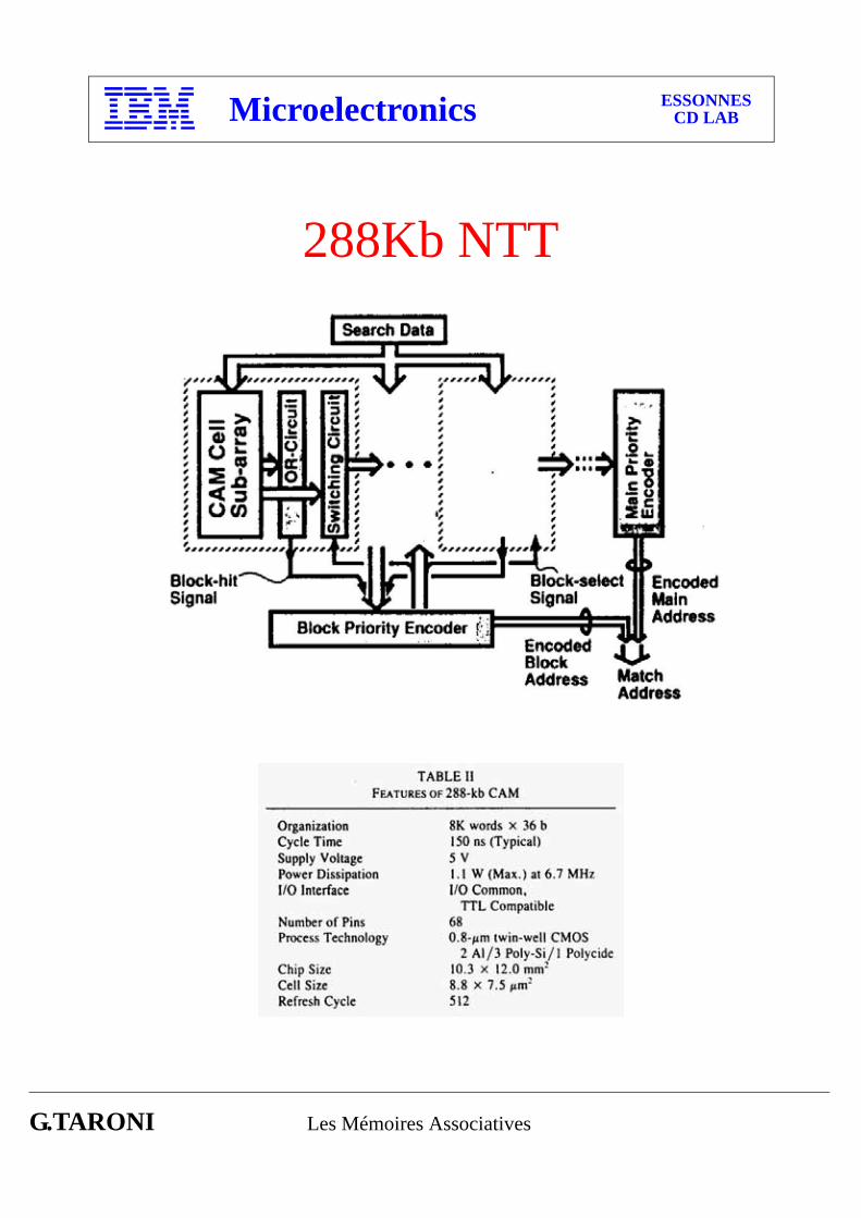
288Kb NTT
G.TARONI Les Mémoires Associatives
Microelectronics ESSONNESCD LAB
288Kb NTT
G.TARONI Les Mémoires Associatives
Microelectronics ESSONNESCD LAB
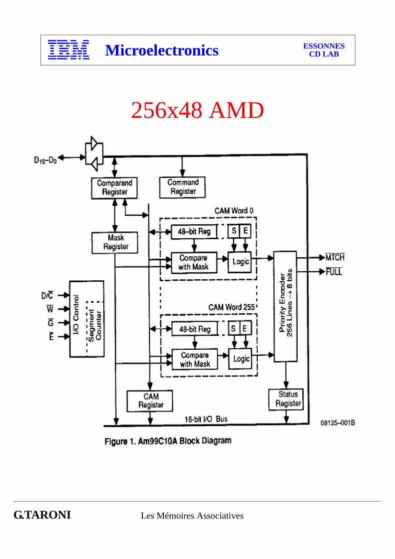
256x48 AMD
G.TARONI Les Mémoires Associatives
Microelectronics ESSONNESCD LAB
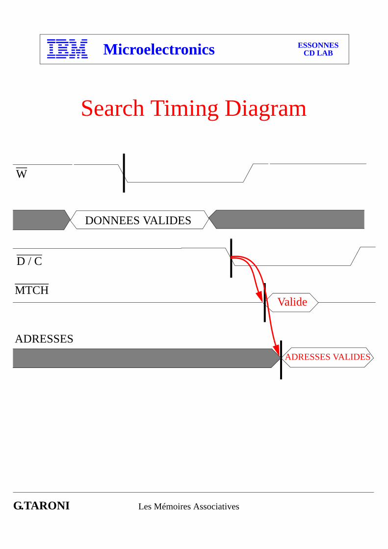
W
DONNEES VALIDES
MTCH Valide
Search Timing Diagram
ADRESSES VALIDES
D / C
ADRESSES
G.TARONI Les Mémoires Associatives
Microelectronics ESSONNESCD LAB
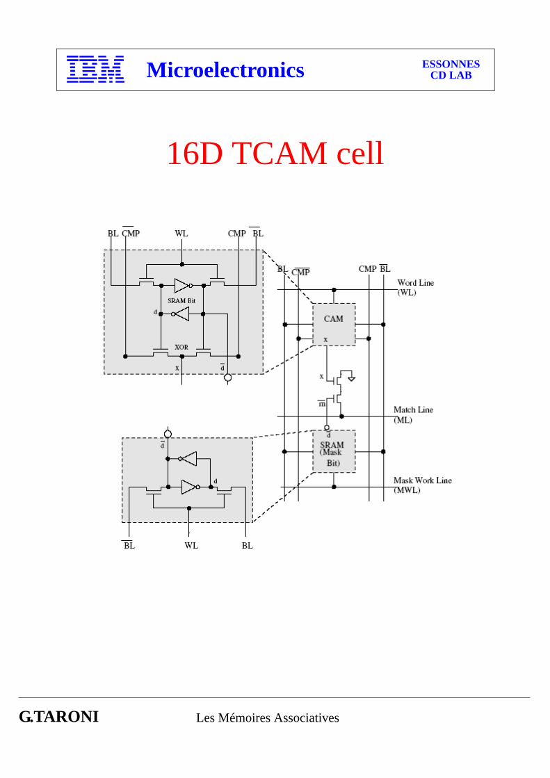
16D TCAM cell
G.TARONI Les Mémoires Associatives
Microelectronics ESSONNESCD LAB
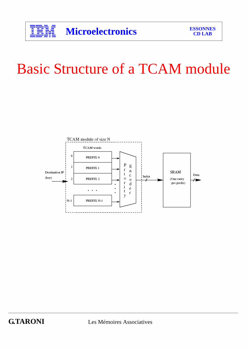
Basic Structure of a TCAM module
G. TARONI Le Test des Mémoires
Microelectronics ESSONNESCD LAB
Test des mémoires
G. TARONI Le Test des Mémoires
Microelectronics ESSONNESCD LAB
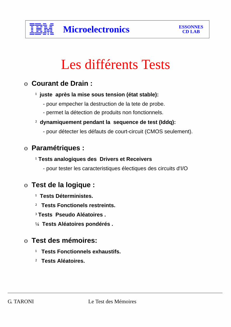
o Courant de Drain :¹ juste après la mise sous tension (état stable):
- pour empecher la destruction de la tete de probe.- permet la détection de produits non fonctionnels.
² dynamiquement pendant la sequence de test (Iddq):- pour détecter les défauts de court-circuit (CMOS seulement).
o Paramétriques :¹ Tests analogiques des Drivers et Receivers
- pour tester les caracteristiques électiques des circuits d'I/O
o Test de la logique :¹ Tests Déterministes.² Tests Fonctionels restreints.³ Tests Pseudo Aléatoires .¼ Tests Aléatoires pondérés .
o Test des mémoires:¹ Tests Fonctionnels exhaustifs.² Tests Aléatoires.
Les différents Tests
G. TARONI Le Test des Mémoires
Microelectronics ESSONNESCD LAB
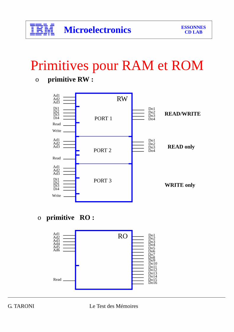
o primitive RW :
RW
o primitive RO :
RO
Ad1Ad2Ad3 Di1Di2Di3Di4Read
Write
Ad1Ad2Ad3
Read
Ad1Ad2Ad3 Di1Di2Di3Di4
Write
Do1Do2Do3Do4
Do1Do2Do3Do4
Ad1Ad2Ad3Ad4Ad5Ad6
Read
Do1Do2Do3Do4Do5Do6Do7Do8Do9Do10Do11Do12Do13Do14Do15Do16
READ/WRITE
READ only
WRITE only
PORT 1
PORT 2
PORT 3
Primitives pour RAM et ROM
G. TARONI Le Test des Mémoires
Microelectronics ESSONNESCD LAB
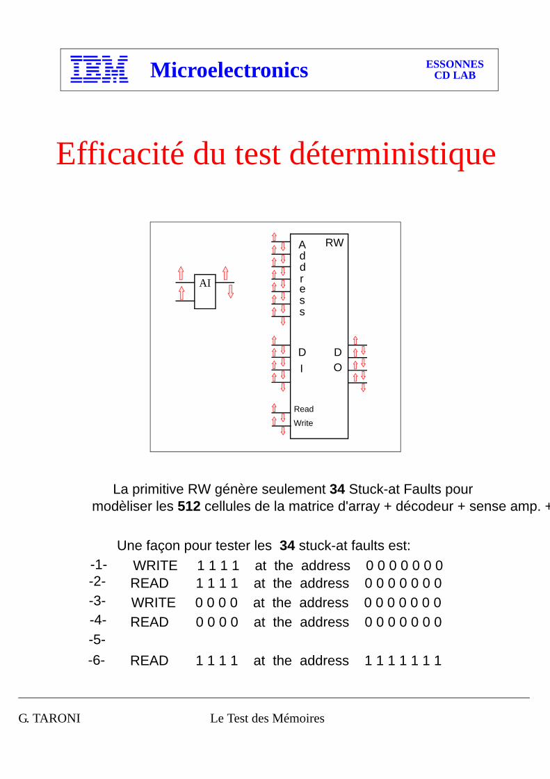
AI
RW
Read
Write
DI
DO
Address
La primitive RW génère seulement 34 Stuck-at Faults pourmodèliser les 512 cellules de la matrice d'array + décodeur + sense amp. +
Une façon pour tester les 34 stuck-at faults est:WRITE 1 1 1 1 at the address 0 0 0 0 0 0 0
WRITE 0 0 0 0 at the address 0 0 0 0 0 0 0 READ 1 1 1 1 at the address 0 0 0 0 0 0 0
READ 0 0 0 0 at the address 0 0 0 0 0 0 0
READ 1 1 1 1 at the address 1 1 1 1 1 1 1
-1--2--3--4--5--6-
Efficacité du test déterministique
G. TARONI Le Test des Mémoires
Microelectronics ESSONNESCD LAB
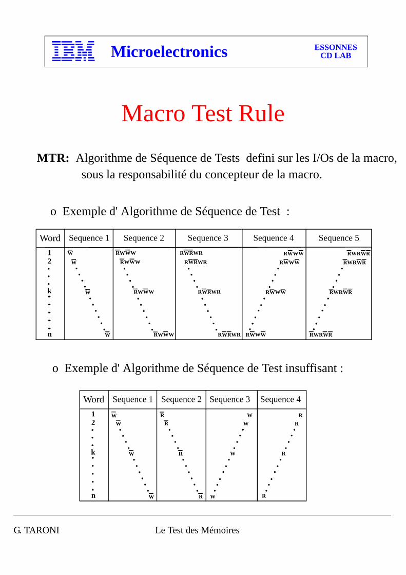
MTR: Algorithme de Séquence de Tests defini sur les I/Os de la macro, sous la responsabilité du concepteur de la macro.
o Exemple d' Algorithme de Séquence de Test :
Word Sequence 1 Sequence 2 Sequence 3 Sequence 4 Sequence 512
k
n
RWWW
RWWW
RWWW
RWWW
RWRWR
RWRWR
RWRWR
RWRWR RWWW
RWWW
RWWWRWWW
RWRWR
RWRWR
RWRWRRWRWR
Word Sequence 1 Sequence 2 Sequence 3 Sequence 412
k
n
RR
R
R W
W
WW
R
RR
R
W
W
W
W
WW
W
W
Macro Test Rule
o Exemple d' Algorithme de Séquence de Test insuffisant :
G. TARONI Le Test des Mémoires
Microelectronics ESSONNESCD LAB
L1L2
L1L2
L1L2 L1
L2
L1L2
L1L2
A
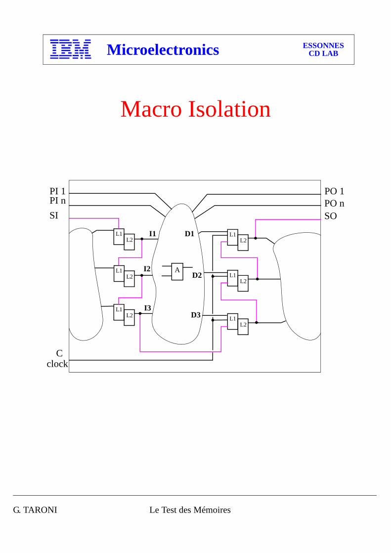
PI 1PI nSI
Cclock
PO 1PO nSO
I1
I2
I3
D1
D2
D3
Macro Isolation
G. TARONI Le Test des Mémoires
Microelectronics ESSONNESCD LAB
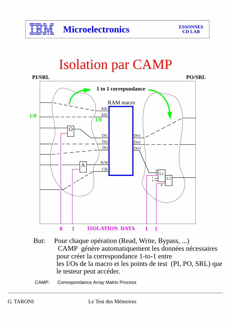
RAM macro
Do1
Do2Do3
Di1Di2Di3
Ad1Ad2
R/W
Clk DC
IA
L1L2
O
A
1 to 1 correpondance
PI/SRL PO/SRL
1/01/0
0 1 1
B
1ISOLATION DATA
But: Pour chaque opération (Read, Write, Bypass, ...) CAMP génère automatiquement les données nécessaires pour créer la correspondance 1-to-1 entreles I/Os de la macro et les points de test (PI, PO, SRL) que le testeur peut accéder.
CAMP: Correspondance Array Matrix Process
Isolation par CAMP
G. TARONI Le Test des Mémoires
Microelectronics ESSONNESCD LAB
Array Built-in Self TestLe contexte:
¹ Limitation du nombre d'I/Os du testeur (Cout).
² Nombre croissant d'I/Os des macros.
³ Des macros de plus en plus importantes.
Les conséquences:
¹ Il n'est pas possible de tester les array-macros à partir des I/Os (PI, PO) du chip.
² Il n'est pas possible de tester les arrays macros en utilisant les SRLs:- trop de temps testeur.- volumes de donnéees importants.- pas d' AC test.
G. TARONI Le Test des Mémoires
Microelectronics ESSONNESCD LAB
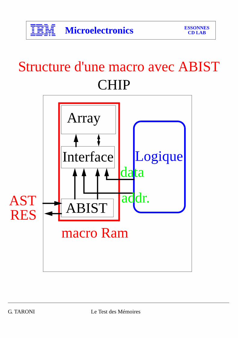
Structure d'une macro avec ABIST
Array
Interface Logique
ABIST
macro Ram
CHIP
ASTRES
data
addr.
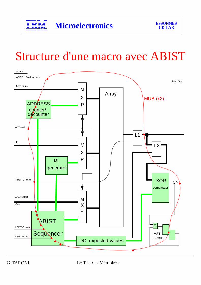
G. TARONI Le Test des Mémoires
Microelectronics ESSONNESCD LAB
L1
L2
XORcomparator
O
ASTResult
DO expected values
Array
MXP
DIgenerator
MXP
Array Select
Cntrl
ABIST
Sequencer
Array C clock
ADDRESScounter/decounter
M
XP
DI
AST mode
Address
ABIST C clock
ABIST B clock
Scan-In
ABIST + RAM A clock
Scan-Out
MUB (x2)
Diag
Structure d'une macro avec ABIST
G. TARONI Le Test des Mémoires
Microelectronics ESSONNESCD LAB
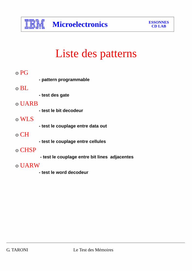
Liste des patternso PG
- pattern programmable
o BL - test des gate
o UARB - test le bit decodeur
o WLS - test le couplage entre data out
o CH - test le couplage entre cellules
o CHSP - test le couplage entre bit lines adjacentes
o UARW - test le word decodeur
G. TARONI Le Test des Mémoires
Microelectronics ESSONNESCD LAB
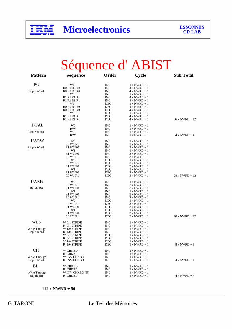
Pattern Sequence Order Cycle Sub/Total
PG W0 INC 1 x NWRD + 1 R0 R0 R0 R0 INC 4 x NWRD + 1
Ripple Word R0 R0 R0 R0 INC 4 x NWRD + 1 W1 INC 1 x NWRD + 1 R1 R1 R1 R1 INC 4 x NWRD + 1R1 R1 R1 R1 INC 4 x NWRD + 1 W0 DEC 1 x NWRD + 1 R0 R0 R0 R0 DEC 4 x NWRD + 1R0 R0 R0 R0 DEC 4 x NWRD + 1 W1 DEC 1 x NWRD + 1 R1 R1 R1 R1 DEC 4 x NWRD + 1R1 R1 R1 R1 DEC 4 x NWRD + 1 36 x NWRD + 12
DUAL W0 INC 1 x NWRD + 1 R/W INC 1 x NWRD + 1
Ripple Word W1 INC 1 x NWRD + 1 R/W INC 1 x NWRD + 1 4 x NWRD + 4
UARW W0 INC 1 x NWRD + 1 R0 W1 R1 INC 3 x NWRD + 1
Ripple Word R1 W0 R0 INC 3 x NWRD + 1 W1 INC 1 x NWRD + 1
R1 W0 R0 INC 3 x NWRD + 1R0 W1 R1 INC 3 x NWRD + 1
W0 DEC 1 x NWRD + 1 R0 W1 R1 DEC 3 x NWRD + 1R1 W0 R0 DEC 3 x NWRD + 1
W1 DEC 1 x NWRD + 1 R1 W0 R0 DEC 3 x NWRD + 1R0 W1 R1 DEC 3 x NWRD + 1 28 x NWRD + 12
UARB W0 INC 1 x NWRD + 1 R0 W1 R1 INC 3 x NWRD + 1
Ripple Bit R1 W0 R0 INC 3 x NWRD + 1 W1 INC 1 x NWRD + 1
R1 W0 R0 INC 3 x NWRD + 1R0 W1 R1 INC 3 x NWRD + 1
W0 DEC 1 x NWRD + 1 R0 W1 R1 DEC 3 x NWRD + 1R1 W0 R0 DEC 3 x NWRD + 1
W1 DEC 1 x NWRD + 1 R1 W0 R0 DEC 3 x NWRD + 1R0 W1 R1 DEC 3 x NWRD + 1 28 x NWRD + 12
WLS W 0/1 STRIPE INC 1 x NWRD + 1 R 0/1 STRIPE INC 1 x NWRD + 1
Write Through W 1/0 STRIPE INC 1 x NWRD + 1 Ripple Word R 1/0 STRIPE INC 1 x NWRD + 1
W 0/1 STRIPE DEC 1 x NWRD + 1 R 0/1 STRIPE DEC 1 x NWRD + 1 W 1/0 STRIPE DEC 1 x NWRD + 1 R 1/0 STRIPE DEC 1 x NWRD + 1 8 x NWRD + 8
CH W CHKBD INC 1 x NWRD + 1 R CHKBD INC 1 x NWRD + 1
Write Through W INV CHKBD INC 1 x NWRD + 1 Ripple Word R INV CHKBD INC 1 x NWRD + 1 4 x NWRD + 4
BL W CHKBD INC 1 x NWRD + 1 R CHKBD INC 1 x NWRD + 1
Write Through W INV CHKBD (N) INC 1 x NWRD + 1 Ripple Bit R CHKBD INC 1 x NWRD + 1 4 x NWRD + 4
112 x NWRD + 56
Séquence d' ABIST
G. TARONI Le Test des Mémoires
Microelectronics ESSONNESCD LAB
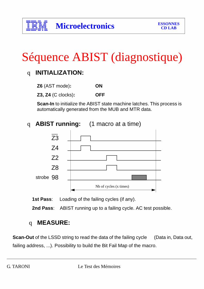
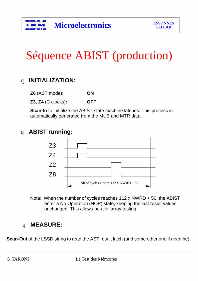
q INITIALIZATION:
Z6 (AST mode): ON
Z3, Z4 (C clocks): OFF
Scan-In to initialize the ABIST state machine latches. This process is automatically generated from the MUB and MTR data.
q ABIST running: (1 macro at a time)
1st Pass: Loading of the failing cycles (if any).
2nd Pass: ABIST running up to a failing cycle. AC test possible.
q MEASURE:
Scan-Out of the LSSD string to read the data of the failing cycle (Data in, Data out,
failing address, ...). Possibility to build the Bit Fail Map of the macro.
Nb of cycles (x times)
Z3Z4Z2Z898strobe
Séquence ABIST (diagnostique)
G. TARONI Le Test des Mémoires
Microelectronics ESSONNESCD LAB
q INITIALIZATION:
Z6 (AST mode): ON
Z3, Z4 (C clocks): OFF
Scan-In to initialize the ABIST state machine latches. This process is automatically generated from the MUB and MTR data.
q ABIST running:
Nota: When the number of cycles reaches 112 x NWRD + 56, the ABIST enter a No Operation (NOP) state, keeping the last result values unchanged. This allows parallel array testing.
q MEASURE:
Scan-Out of the LSSD string to read the AST result latch (and some other one if need be).
Nb of cycles > or = 112 x NWRD + 56
Z3Z4Z2Z8
Séquence ABIST (production)
G. TARONI Le Test des Mémoires
Microelectronics ESSONNESCD LAB
ABIST overview o utilisé pour les mémoires intégrées o circuits inclus dans la macro o tests tous les features de la RAM o pour les RAM avec redondance , l' ABIST conserve les adresses de fail o concept utilisé au niveau chip , carte et système
o tests déterministiques o toutes les RAM d'un meme chip sont testées en parallèle
o AC test possible
G. TARONI Le Test des Mémoires
Microelectronics ESSONNESCD LAB
L1
L2
A
L1
L2
AL1
L2
A
L1
L2
A
L1
L2
ODO1
DI1
A
A A A A
NAd1
NAd2
AAA
A
ASelect
Read
Write
L1
L2
A
L1
L2
AL1
L2
A
L1
L2
A
L1
L2
ODO2
DI2
L1/L2 L1/L2*improvement:
SO
SI
00 01 10 11
L1
L2
A
L1
L2
AL1
L2
A
L1
L2
A
L1
L2
ODO3
DI3
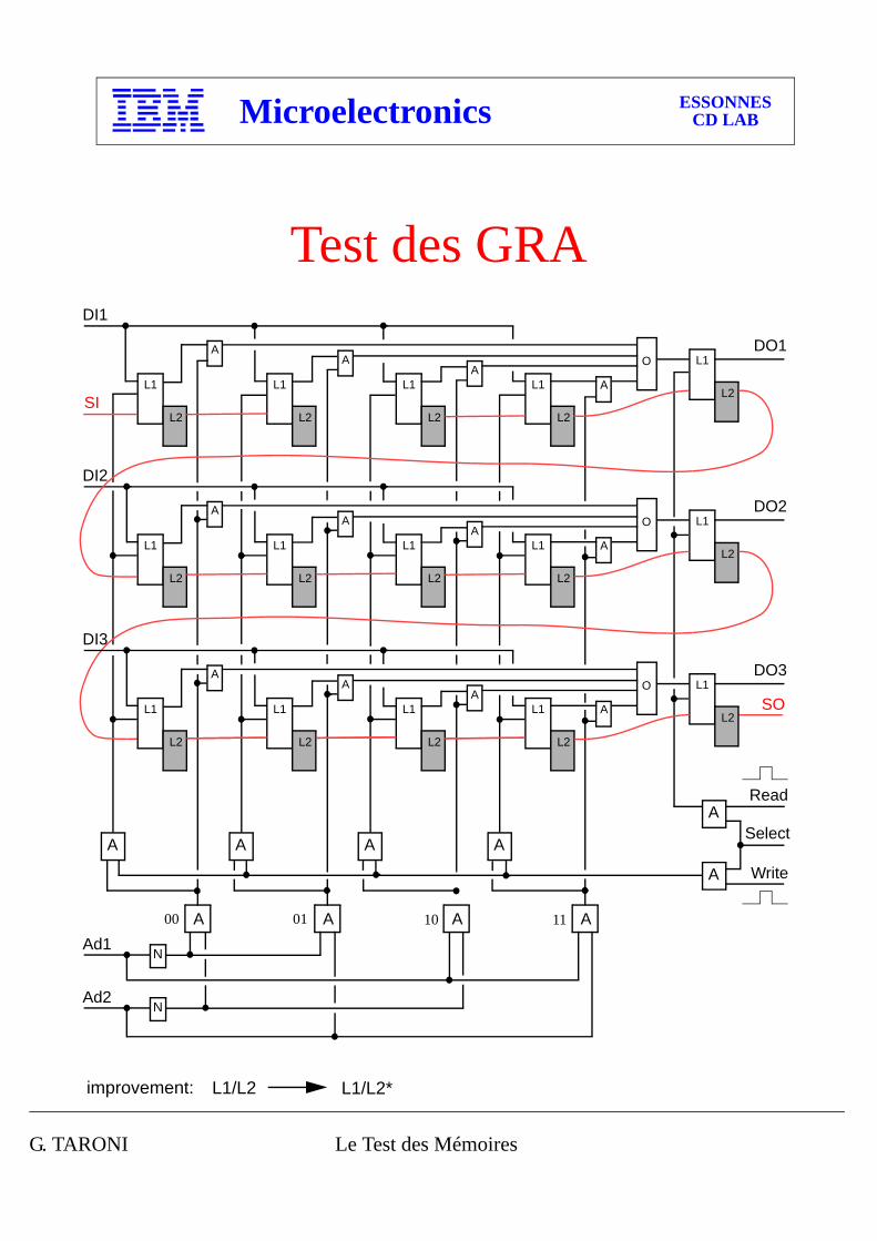
Test des GRA
G. TARONI Le Test des Mémoires
Microelectronics ESSONNESCD LAB
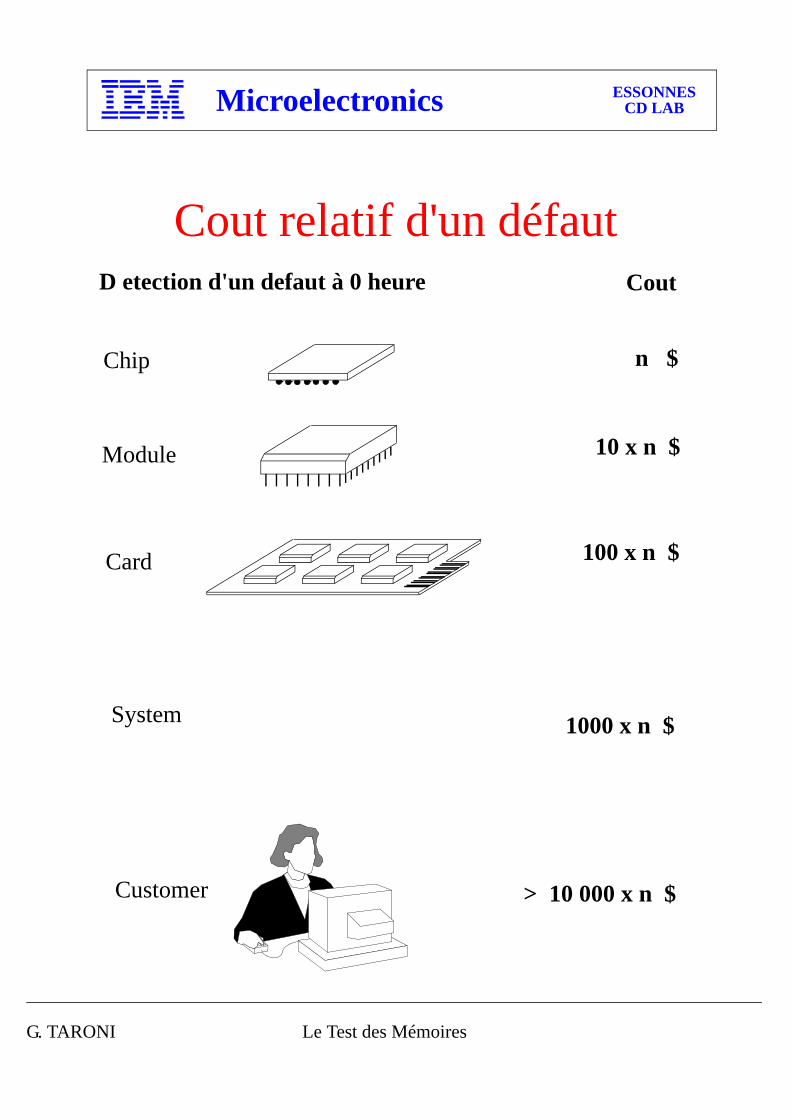
D etection d'un defaut à 0 heure Cout
Chip
Module
Card
System
Customer
n $
10 x n $
100 x n $
1000 x n $
> 10 000 x n $
Cout relatif d'un défaut
G. TARONI Les Mémoires Intégrées
Microelectronics ESSONNESCD LAB
Les Mémoires Intégrées
G. TARONI Les Mémoires Intégrées
Microelectronics ESSONNESCD LAB
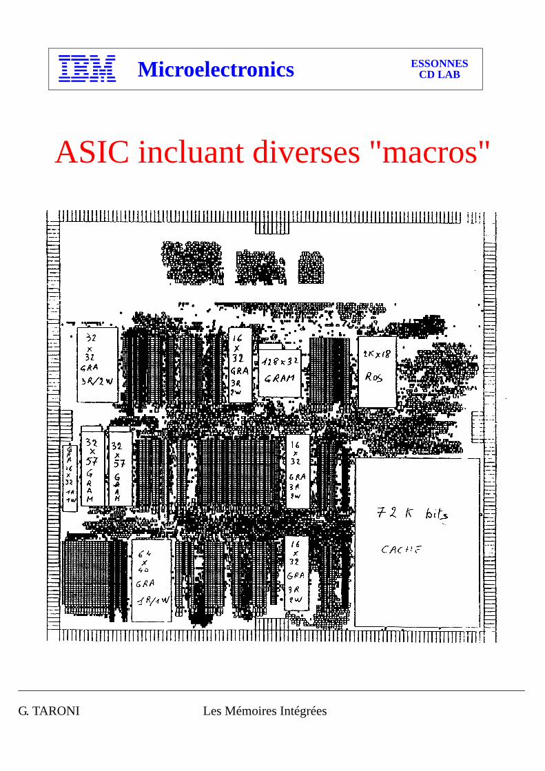
ASIC incluant diverses "macros"
G. TARONI Les Mémoires Intégrées
Microelectronics ESSONNESCD LAB
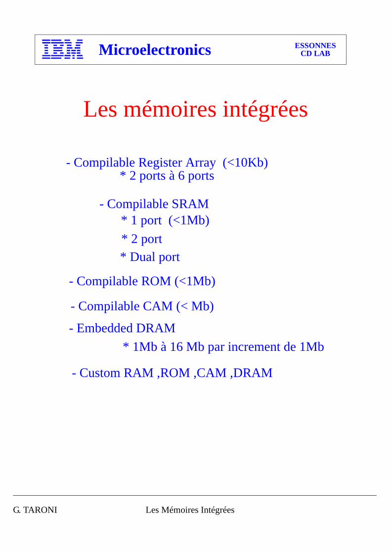
Les mémoires intégrées
- Compilable Register Array (<10Kb)
- Compilable SRAM
- Compilable ROM (<1Mb)
* 2 ports à 6 ports
- Custom RAM ,ROM ,CAM ,DRAM
* 1 port (<1Mb)
* 1Mb à 16 Mb par increment de 1Mb- Embedded DRAM
* 2 port * Dual port
- Compilable CAM (< Mb)
G. TARONI Les Mémoires Intégrées
Microelectronics ESSONNESCD LAB
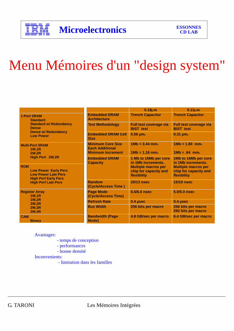
Menu Mémoires d'un "design system"
Avantages: - temps de conception - performances - bonne densité Inconvenients: - limitation dans les familles
1-Port SRAM Standard Standard w/ Redundancy Dense Dense w/ Redundancy Low Power
Multi-Port SRAM 1W,1R 2W,2R High Perf. 2W,2R
ROM Low Power Early Pers Low Power Late Pers High Perf Early Pers High Perf Late Pers
Register Array 1W,1R 1W,2R 2W,2R 2W,3R 2W,4RCAM Binary
0.18µm 0.13µmEmbedded DRAM Architecture
Trench Capacitor Trench Capacitor
Test Methodology Full test coverage via BIST test
Full test coverage via BIST test
Embedded DRAM Cell Size
0.56 µm2 0.31 µm2
Minimum Core SizeEach Additional Minimum Increment
1Mb = 3.44 mm2
1Mb = 1.16 mm2
1Mb = 1.80 mm2
1Mb = .64 mm2
Embedded DRAM Capacity
1 Mb to 16Mb per core in 1Mb increments. Multiple macros per chip for capacity and flexibility
1Mb to 16Mb per core in 1Mb increments. Multiple macros per chip for capacity and flexibility
Random (Cycle/Access Time )
20/13 nsec 15/10 nsec
Page Mode (Cycle/Access Time)
6.6/6.6 nsec 5.0/5.0 nsec
Refresh Rate 0.4 µsec 0.4 µsecBus Width 256 bits per macro 256 bits per macro
292 bits per macroBandwidth (Page Mode)
4.8 GB/sec per macro 6.4 GB/sec per macro
G. TARONI Les Mémoires Intégrées
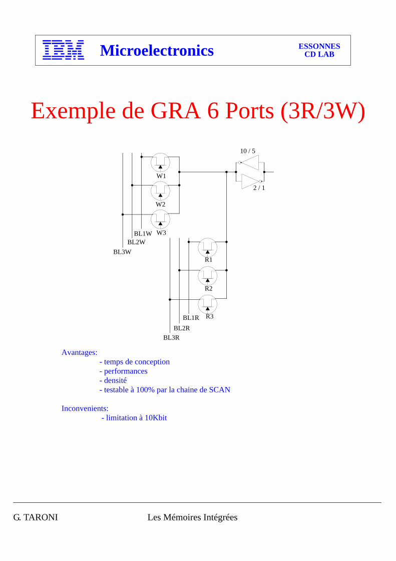
Microelectronics ESSONNESCD LAB
Exemple de GRA 6 Ports (3R/3W)
W1
W2
W3BL1WBL2W
BL3W
BL1RBL2R
BL3R
R1
R2
R3
2 / 1
10 / 5
Avantages: - temps de conception - performances - densité - testable à 100% par la chaine de SCAN
Inconvenients: - limitation à 10Kbit
G. TARONI Les Mémoires Intégrées
Microelectronics ESSONNESCD LAB
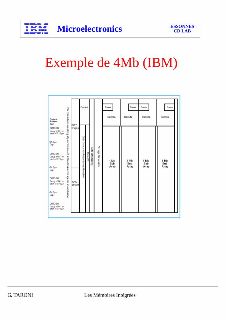
Exemple de 4Mb (IBM)
G. TARONI Les Mémoires Intégrées
Microelectronics ESSONNESCD LAB
L’ère des eFLASH
• MEILLEURES PERFORMANCES (INTERFACE SUPPRIMEE)
• REDUCTION DE LA PUISSANCE CONSOMMEE ET DU BRUIT
• DIMINUTION DE LA SURFACE SUR LES BOARDS
• SECURITE DES DONNEES ACCRUES (SMART CARDS)
• COUT ?
• PROCEDE PLUS COMPLEXE ET PLUS ONEREUX
• TESTS (24H @ 250°C)
G. TARONI Les Mémoires Intégrées
Microelectronics ESSONNESCD LAB
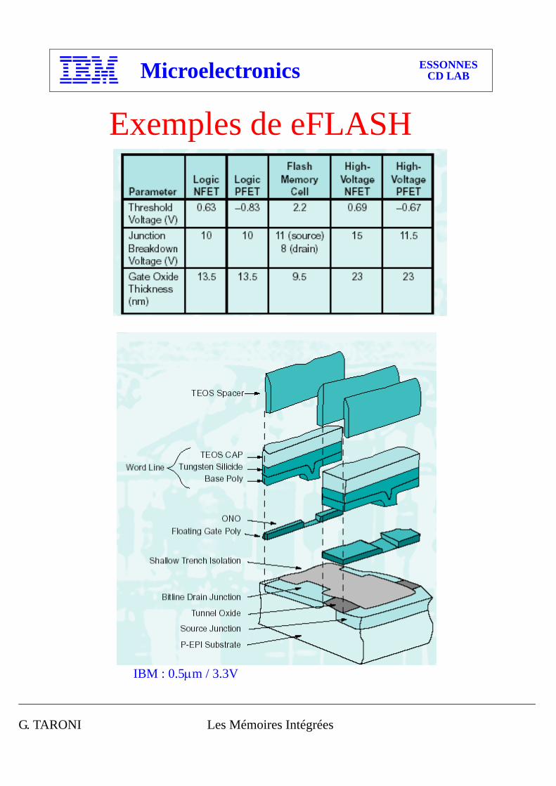
Exemples de eFLASH
IBM : 0.5µm / 3.3V
G. TARONI Les Mémoires Intégrées
Microelectronics ESSONNESCD LAB
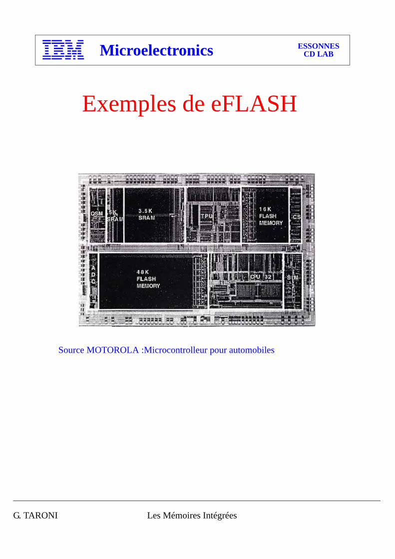
Exemples de eFLASH
Source MOTOROLA :Microcontrolleur pour automobiles
G. TARONI Les Mémoires Intégrées
Microelectronics ESSONNESCD LAB
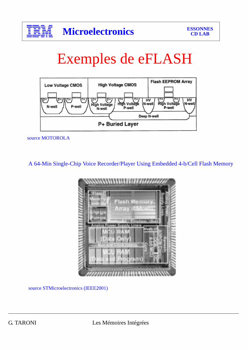
source MOTOROLA
source STMicroelectronics (IEEE2001)
A 64-Min Single-Chip Voice Recorder/Player Using Embedded 4-b/Cell Flash Memory
Exemples de eFLASH
G. TARONI Les Mémoires Intégrées
Microelectronics ESSONNESCD LAB
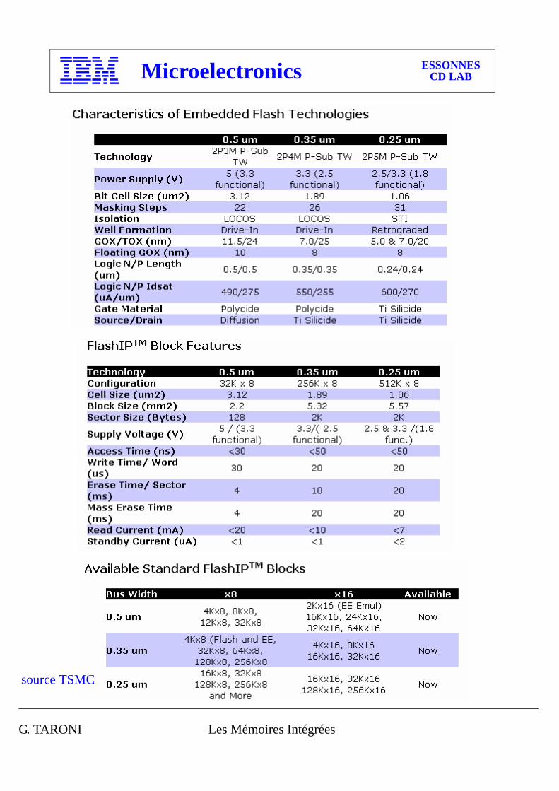
source TSMC
G.TARONI Conclusions
Microelectronics ESSONNESCD LAB
Conclusions
G.TARONI Conclusions
Microelectronics ESSONNESCD LAB
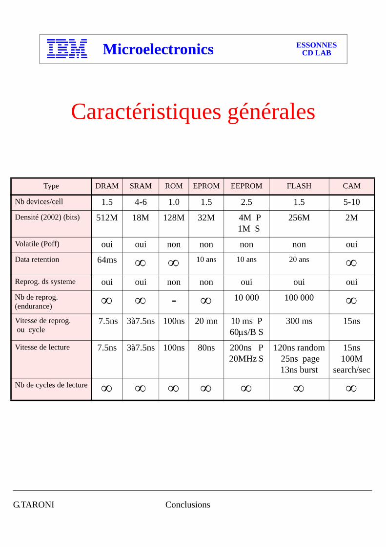
Caractéristiques générales
Type DRAM SRAM ROM EPROM EEPROM FLASH CAM
Nb devices/cell 1.5 4-6 1.0 1.5 2.5 1.5 5-10Densité (2002) (bits) 512M 18M 128M 32M 4M P
1M S256M 2M
Volatile (Poff) oui oui non non non non ouiData retention 64ms ∞ ∞ 10 ans 10 ans 20 ans ∞Reprog. ds systeme oui oui non non oui oui ouiNb de reprog.(endurance) ∞ ∞ - ∞ 10 000 100 000 ∞Vitesse de reprog. ou cycle
7.5ns 3à7.5ns 100ns 20 mn 10 ms P60µs/B S
300 ms 15ns
Vitesse de lecture 7.5ns 3à7.5ns 100ns 80ns 200ns P20MHz S
120ns random 25ns page13ns burst
15ns100M
search/secNb de cycles de lecture ∞ ∞ ∞ ∞ ∞ ∞ ∞
G.TARONI Conclusions
Microelectronics ESSONNESCD LAB
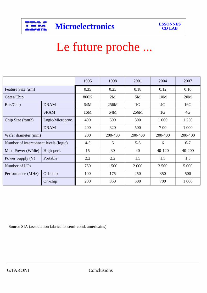
Le future proche ...
1995 1998 2001 2004 2007
Feature Size (µm) 0.35 0.25 0.18 0.12 0.10
Gates/Chip 800K 2M 5M 10M 20M
Bits/Chip DRAM 64M 256M 1G 4G 16G
SRAM 16M 64M 256M 1G 4G
Chip Size (mm2) Logic/Microproc. 400 600 800 1 000 1 250
DRAM 200 320 500 7 00 1 000
Wafer diameter (mm) 200 200-400 200-400 200-400 200-400
Number of interconnect levels (logic) 4-5 5 5-6 6 6-7
Max. Power (W/die) High-perf. 15 30 40 40-120 40-200
Power Supply (V) Portable 2.2 2.2 1.5 1.5 1.5
Number of I/Os 750 1 500 2 000 3 500 5 000
Performance (MHz) Off-chip 100 175 250 350 500
On-chip 200 350 500 700 1 000
Source SIA (association fabricants semi-cond. américains)