Embed Size (px)
Citation preview
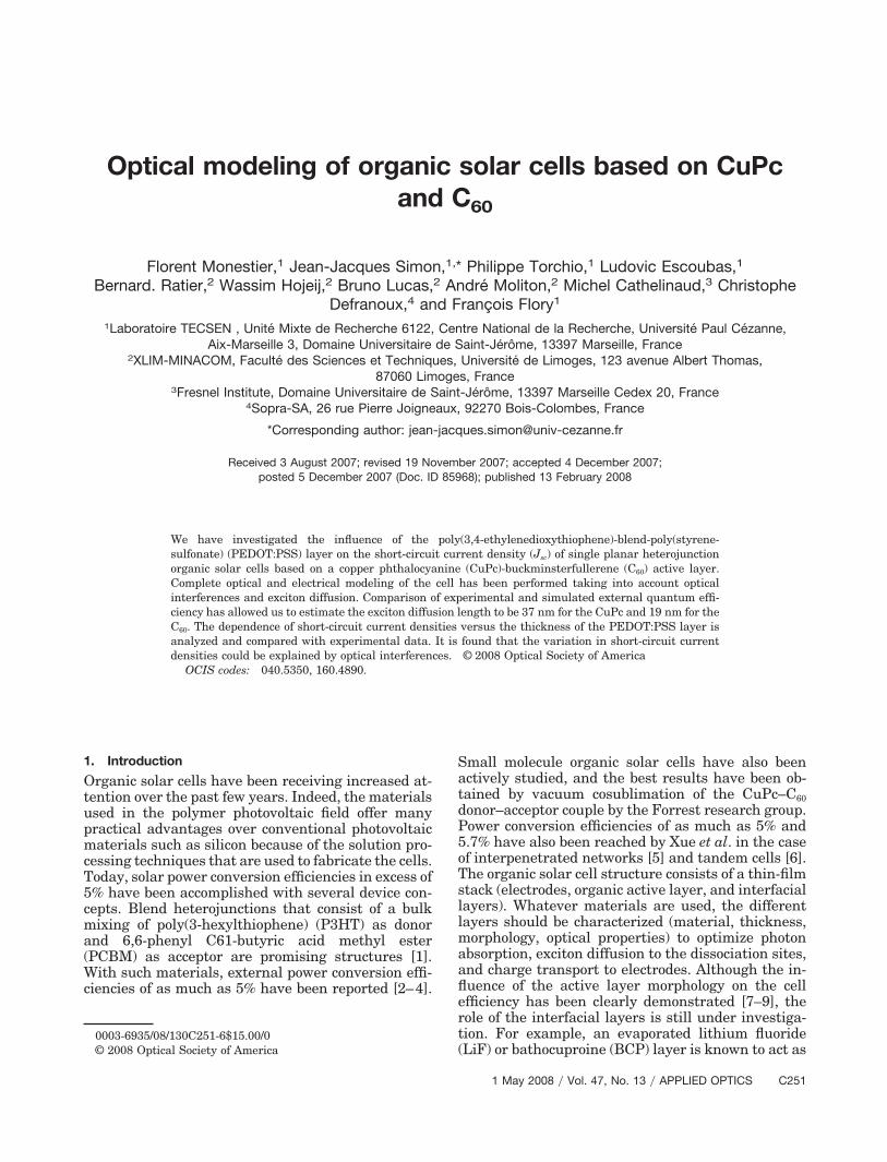
Optical modeling of organic solar cells based on CuPcand C60
Florent Monestier,1 Jean-Jacques Simon,1,* Philippe Torchio,1 Ludovic Escoubas,1
Bernard. Ratier,2 Wassim Hojeij,2 Bruno Lucas,2 André Moliton,2 Michel Cathelinaud,3 ChristopheDefranoux,4 and François Flory1
1Laboratoire TECSEN , Unité Mixte de Recherche 6122, Centre National de la Recherche, Université Paul Cézanne,Aix-Marseille 3, Domaine Universitaire de Saint-Jérôme, 13397 Marseille, France
2XLIM-MINACOM, Faculté des Sciences et Techniques, Université de Limoges, 123 avenue Albert Thomas,87060 Limoges, France
3Fresnel Institute, Domaine Universitaire de Saint-Jérôme, 13397 Marseille Cedex 20, France4Sopra-SA, 26 rue Pierre Joigneaux, 92270 Bois-Colombes, France
*Corresponding author: [email protected]
Received 3 August 2007; revised 19 November 2007; accepted 4 December 2007;posted 5 December 2007 (Doc. ID 85968); published 13 February 2008
We have investigated the influence of the poly(3,4-ethylenedioxythiophene)-blend-poly(styrene-sulfonate) (PEDOT:PSS) layer on the short-circuit current density (Jsc) of single planar heterojunctionorganic solar cells based on a copper phthalocyanine (CuPc)-buckminsterfullerene (C60) active layer.Complete optical and electrical modeling of the cell has been performed taking into account opticalinterferences and exciton diffusion. Comparison of experimental and simulated external quantum effi-ciency has allowed us to estimate the exciton diffusion length to be 37 nm for the CuPc and 19 nm for theC60. The dependence of short-circuit current densities versus the thickness of the PEDOT:PSS layer isanalyzed and compared with experimental data. It is found that the variation in short-circuit currentdensities could be explained by optical interferences. © 2008 Optical Society of America
OCIS codes: 040.5350, 160.4890.
1. Introduction
Organic solar cells have been receiving increased at-tention over the past few years. Indeed, the materialsused in the polymer photovoltaic field offer manypractical advantages over conventional photovoltaicmaterials such as silicon because of the solution pro-cessing techniques that are used to fabricate the cells.Today, solar power conversion efficiencies in excess of5% have been accomplished with several device con-cepts. Blend heterojunctions that consist of a bulkmixing of poly(3-hexylthiophene) (P3HT) as donorand 6,6-phenyl C61-butyric acid methyl ester(PCBM) as acceptor are promising structures [1].With such materials, external power conversion effi-ciencies of as much as 5% have been reported [2–4].
Small molecule organic solar cells have also beenactively studied, and the best results have been ob-tained by vacuum cosublimation of the CuPc–C60donor–acceptor couple by the Forrest research group.Power conversion efficiencies of as much as 5% and5.7% have also been reached by Xue et al. in the caseof interpenetrated networks [5] and tandem cells [6].The organic solar cell structure consists of a thin-filmstack (electrodes, organic active layer, and interfaciallayers). Whatever materials are used, the differentlayers should be characterized (material, thickness,morphology, optical properties) to optimize photonabsorption, exciton diffusion to the dissociation sites,and charge transport to electrodes. Although the in-fluence of the active layer morphology on the cellefficiency has been clearly demonstrated [7–9], therole of the interfacial layers is still under investiga-tion. For example, an evaporated lithium fluoride(LiF) or bathocuproine (BCP) layer is known to act as
0003-6935/08/130C251-6$15.00/0© 2008 Optical Society of America
1 May 2008 � Vol. 47, No. 13 � APPLIED OPTICS C251
a protective layer between the electrode and the or-ganic material. Brabec et al. [10] have shown that theinsertion of this LiF interlayer under the negativemetal electrode significantly enhances the fill factor(FF) and stabilizes high open circuit voltages (Voc).Insertion of a BCP thin film as an electron transport-ing layer between the C60 and the metal cathode wasalso proposed for efficient electron collection by Yooet al. [11]. With regard to the indium tin oxide (ITO)electrode, the most widely used cover layer is a trans-parent composite PEDOT:PSS, which acts as a near-transparent hole transport and injection layer andenhances the reproducibility and the performance ofthe devices. The thickness of the PEDOT:PSS de-pends on the roughness of the ITO. It has recentlybeen shown that the ITO anode obtained by ion beamsputtering (IBS) has permitted a decrease in thePEDOT:PSS layer thickness, leading to power con-version efficiency of 1.3% [12]. Here we investigateoptimization of the PEDOT:PSS thickness layerthrough optical and electrical modeling of organicsolar cells based on CuPc and C60. This allows us tounderstand more precisely the influence of chargetransport in single planar heterojunction organic so-lar cells based on a CuPc-C60 active layer. We beginby presenting a characterization of the optical con-stants of the layers. Such knowledge creates thepossibility to compute the electromagnetic field dis-tribution in the whole structure and the energy ab-sorbed inside the active area by taking into accountinterference effects. We then provide the generationrate distribution inside the active C60. Finally, wededuce the diffusion lengths of CuPc and C60 by acomparison of simulated photocurrent and experi-mental data that allows us to distinguish the contri-bution of the optical part of PEDOT:PSS from theelectrical part.
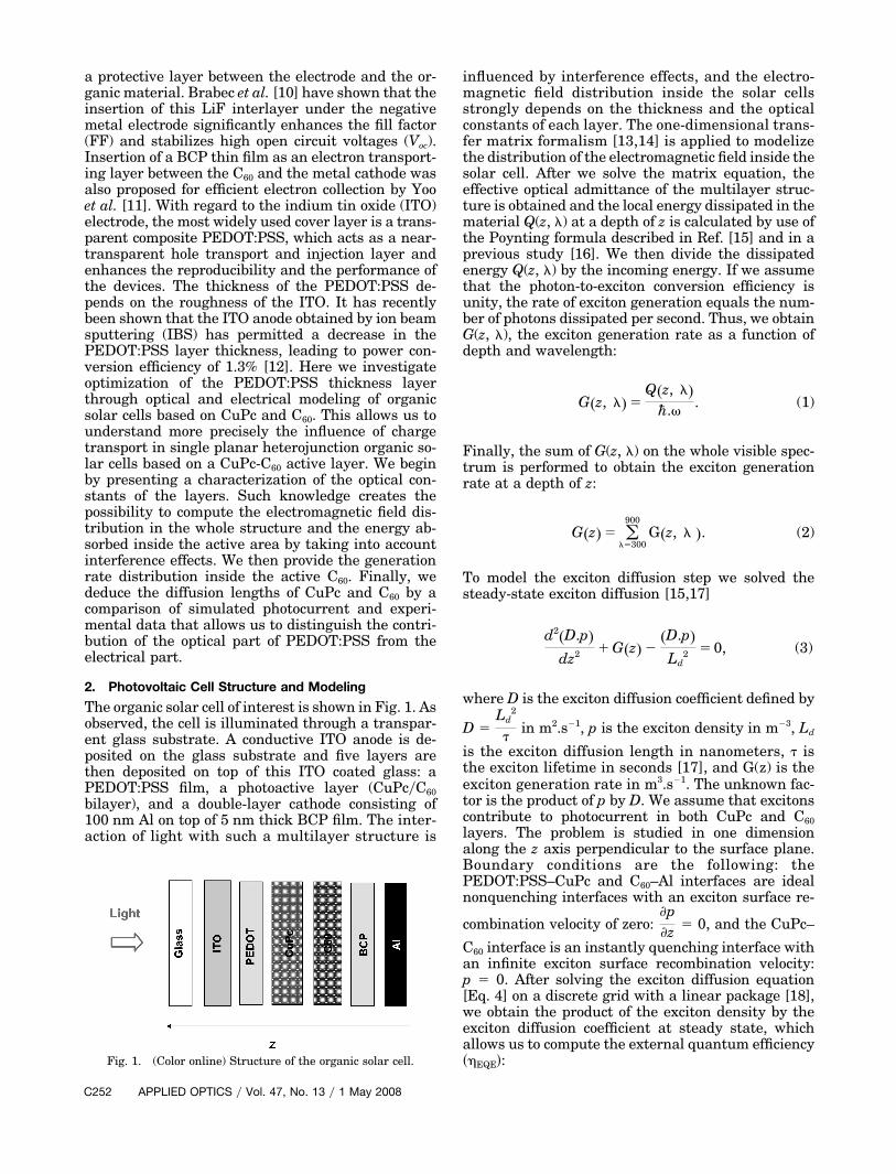
2. Photovoltaic Cell Structure and Modeling
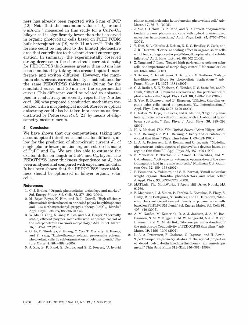
The organic solar cell of interest is shown in Fig. 1. Asobserved, the cell is illuminated through a transpar-ent glass substrate. A conductive ITO anode is de-posited on the glass substrate and five layers arethen deposited on top of this ITO coated glass: aPEDOT:PSS film, a photoactive layer (CuPc�C60bilayer), and a double-layer cathode consisting of100 nm Al on top of 5 nm thick BCP film. The inter-action of light with such a multilayer structure is
influenced by interference effects, and the electro-magnetic field distribution inside the solar cellsstrongly depends on the thickness and the opticalconstants of each layer. The one-dimensional trans-fer matrix formalism [13,14] is applied to modelizethe distribution of the electromagnetic field inside thesolar cell. After we solve the matrix equation, theeffective optical admittance of the multilayer struc-ture is obtained and the local energy dissipated in thematerial Q(z, �) at a depth of z is calculated by use ofthe Poynting formula described in Ref. [15] and in aprevious study [16]. We then divide the dissipatedenergy Q(z, �) by the incoming energy. If we assumethat the photon-to-exciton conversion efficiency isunity, the rate of exciton generation equals the num-ber of photons dissipated per second. Thus, we obtainG(z, �), the exciton generation rate as a function ofdepth and wavelength:
G�z, �� �Q�z, ��
�h.� . (1)
Finally, the sum of G(z, �) on the whole visible spec-trum is performed to obtain the exciton generationrate at a depth of z:
G�z� � ���300
900
G�z, � �. (2)
To model the exciton diffusion step we solved thesteady-state exciton diffusion [15,17]
d2�D.p�dz2 � G�z� �
�D.p�Ld
2 � 0, (3)
where D is the exciton diffusion coefficient defined by
D �Ld
2
�in m2.s�1, p is the exciton density in m�3, Ld
is the exciton diffusion length in nanometers, � isthe exciton lifetime in seconds [17], and G(z) is theexciton generation rate in m3.s�1. The unknown fac-tor is the product of p by D. We assume that excitonscontribute to photocurrent in both CuPc and C60layers. The problem is studied in one dimensionalong the z axis perpendicular to the surface plane.Boundary conditions are the following: thePEDOT:PSS–CuPc and C60–Al interfaces are idealnonquenching interfaces with an exciton surface re-
combination velocity of zero:�p�z � 0, and the CuPc–
C60 interface is an instantly quenching interface withan infinite exciton surface recombination velocity:p � 0. After solving the exciton diffusion equation[Eq. 4] on a discrete grid with a linear package [18],we obtain the product of the exciton density by theexciton diffusion coefficient at steady state, whichallows us to compute the external quantum efficiency��EQE�:Fig. 1. (Color online) Structure of the organic solar cell.
C252 APPLIED OPTICS � Vol. 47, No. 13 � 1 May 2008
�EQE �1N���D.p�
�z �z�junction�
�1N���D.p�
�z �z�junction�
, (4)
where the minus and plus signs refer, respectively,to the acceptor (C60) and the donor (CuPc) layer, N isthe number of incident photons per square meter andper second. These two terms are related to the deriv-ative of the exciton distribution at the CuPc–C60 in-terface. The short-circuit current density Jsc iscomputed in the same way as in the formula: JSC� q.�EQE.N.
3. Experimental Details
The ITO coating on glass substrates was done in thelaboratory by IBS, the details of which are given in Ref.[12]. The PEDOT:PSS Baytron PH layer from H. C.Starck (Newton, Massachusetts, USA) was spin coatedon the ITO-coated glass substrates, acting as a holetransport layer and preventing oxygen diffusion fromITO into the active layer. Copper phthalocyanine(CuPc) molecules of 99.5% purity were purchased fromSigma-Aldrich (St. Louis, Missouri, USA) and 99.9 %pure fullerene C60 was purchased from MER Corpo-ration (Tucson, Arizona, USA). The BCP that we usedas optional exciton blocking layers (5 nm) prior todeposition of the top aluminum cathode was providedby Aldrich. These products were deposited withoutadditional purification. The successive CuPc and C60vacuum sublimation was performed in our home-made coevaporation set up (by the Joule effect), andthe growth rates were kept to 0.08 nm�s and0.1 nm�s for CuPc and C60, respectively. The alumi-num top electrode contact is deposited in an in situconfined bench through a shadow mask that delimitsa 0.25 cm2 diode area according to the setup shownin Ref. [9]. I(V) measurements were taken withan SMU2400 SourceMeter (Keithley Instruments,Cleveland, Ohio, USA) in the dark or under AM1.5illumination 94 mW�cm2) with an Atlas Solar Con-stant 575PV simulator. The external quantum effi-ciency (EQE) spectra of the solar cells were takenunder excitation of a TS-428 Acton 250 W tungstenhalogen lamp supplied by a JQE 25-10 M voltage unit(Kepco, Flushing, New York, USA) and made mono-
chromatic by use of a SpectraPro 2150i (Acton Re-search, Acton, Massachusetts, USA) at a 80 Hzchopping frequency. The photocurrent is detected bya Stanford Research SR530 lock-in amplifier andcompared with the signal obtained under the sameillumination conditions by a Hamamatsu large areaphotodiode whose spectral response is given by theconstructor. Taking into account the glass transmit-tance (90% in the UV–visible range) of this test boxand the use of a borosilicate UV filter, the incidentlight flux was limited to 84.6 mW�cm2.
4. Results and Discussion
A. Optical Constants
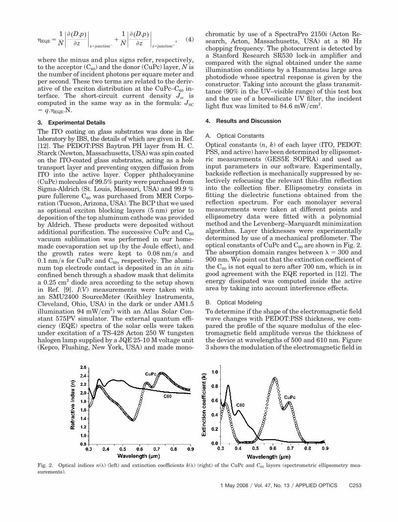
Optical constants (n, k) of each layer (ITO, PEDOT:PSS, and active) have been determined by ellipsomet-ric measurements (GES5E SOPRA) and used asinput parameters in our software. Experimentally,backside reflection is mechanically suppressed by se-lectively refocusing the relevant thin-film reflectioninto the collection fiber. Ellipsometry consists infitting the dielectric functions obtained from thereflection spectrum. For each monolayer severalmeasurements were taken at different points andellipsometry data were fitted with a polynomialmethod and the Levenberg–Marquardt minimizationalgorithm. Layer thicknesses were experimentallydetermined by use of a mechanical profilometer. Theoptical constants of CuPc and C60 are shown in Fig. 2.The absorption domain ranges between � � 300 and900 nm. We point out that the extinction coefficient ofthe C60 is not equal to zero after 700 nm, which is ingood agreement with the EQE reported in [12]. Theenergy dissipated was computed inside the activearea by taking into account interference effects.
B. Optical Modeling
To determine if the shape of the electromagnetic fieldwave changes with PEDOT:PSS thickness, we com-pared the profile of the square modulus of the elec-tromagnetic field amplitude versus the thickness ofthe device at wavelengths of 500 and 610 nm. Figure3 shows the modulation of the electromagnetic field in
Fig. 2. Optical indices n(�) (left) and extinction coefficients k(�) (right) of the CuPc and C60 layers (spectrometric ellipsometry mea-surements).
1 May 2008 � Vol. 47, No. 13 � APPLIED OPTICS C253
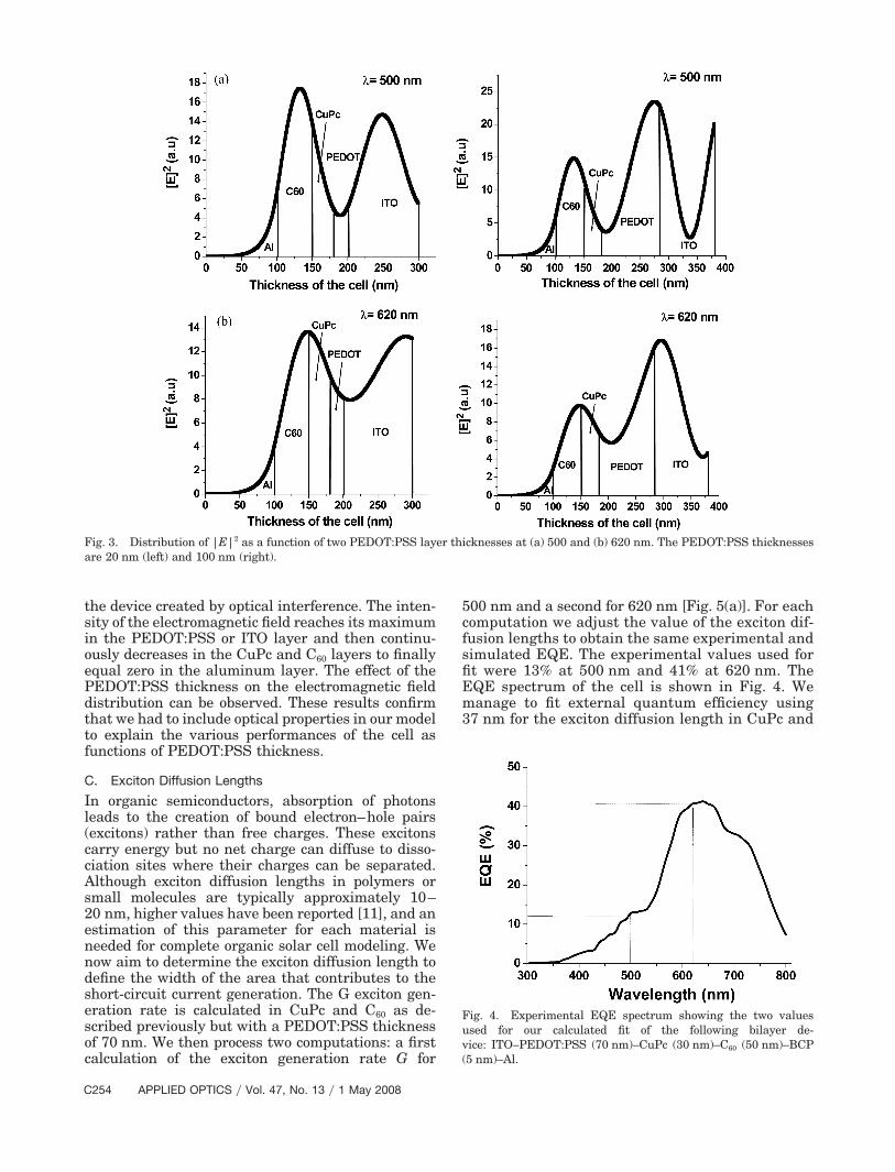
the device created by optical interference. The inten-sity of the electromagnetic field reaches its maximumin the PEDOT:PSS or ITO layer and then continu-ously decreases in the CuPc and C60 layers to finallyequal zero in the aluminum layer. The effect of thePEDOT:PSS thickness on the electromagnetic fielddistribution can be observed. These results confirmthat we had to include optical properties in our modelto explain the various performances of the cell asfunctions of PEDOT:PSS thickness.
C. Exciton Diffusion Lengths
In organic semiconductors, absorption of photonsleads to the creation of bound electron–hole pairs(excitons) rather than free charges. These excitonscarry energy but no net charge can diffuse to disso-ciation sites where their charges can be separated.Although exciton diffusion lengths in polymers orsmall molecules are typically approximately 10–20 nm, higher values have been reported [11], and anestimation of this parameter for each material isneeded for complete organic solar cell modeling. Wenow aim to determine the exciton diffusion length todefine the width of the area that contributes to theshort-circuit current generation. The G exciton gen-eration rate is calculated in CuPc and C60 as de-scribed previously but with a PEDOT:PSS thicknessof 70 nm. We then process two computations: a firstcalculation of the exciton generation rate G for
500 nm and a second for 620 nm [Fig. 5(a)]. For eachcomputation we adjust the value of the exciton dif-fusion lengths to obtain the same experimental andsimulated EQE. The experimental values used forfit were 13% at 500 nm and 41% at 620 nm. TheEQE spectrum of the cell is shown in Fig. 4. Wemanage to fit external quantum efficiency using37 nm for the exciton diffusion length in CuPc and
Fig. 3. Distribution of |E|2 as a function of two PEDOT:PSS layer thicknesses at (a) 500 and (b) 620 nm. The PEDOT:PSS thicknessesare 20 nm (left) and 100 nm (right).
Fig. 4. Experimental EQE spectrum showing the two valuesused for our calculated fit of the following bilayer de-vice: ITO–PEDOT:PSS (70 nm)–CuPc (30 nm)–C60 (50 nm)–BCP(5 nm)–Al.
C254 APPLIED OPTICS � Vol. 47, No. 13 � 1 May 2008
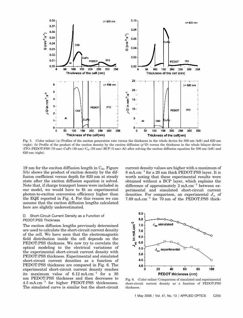
19 nm for the exciton diffusion length in C60. Figure5(b) shows the product of exciton density by the dif-fusion coefficient versus depth for 620 nm at steadystate after the exciton diffusion equation is solved.Note that, if charge transport losses were included inour model, we would have to fit an experimentalphoton-to-exciton conversion efficiency higher thanthe EQE reported in Fig. 4. For this reason we canassume that the exciton diffusion lengths calculatedhere are slightly underestimated.
D. Short-Circuit Current Density as a Function ofPEDOT:PSS Thickness
The exciton diffusion lengths previously determinedare used to calculate the short-circuit current densityof the cell. We have seen that the electromagneticfield distribution inside the cell depends on thePEDOT:PSS thickness. We now try to correlate theoptical modeling to the electrical variations ofthe experimental short-circuit current density withPEDOT:PSS thickness. Experimental and simulatedshort-circuit current densities as a function ofPEDOT:PSS thickness are compared in Fig. 6. Theexperimental short-circuit current density reachesits maximum value of 6.12 mA.cm�2 for a 30nm PEDOT:PSS thickness and then decreases to4.5 mA.cm�2 for higher PEDOT:PSS thicknesses.The simulated curve is similar but the short-circuit
current density values are higher with a maximum of8 mA.cm�2 for a 20 nm thick PEDOT:PSS layer. It isworth noting that these experimental results wereobtained without a BCP layer, which explains thedifference of approximately 2 mA.cm�2 between ex-perimental and simulated short-circuit currentdensities. For comparison, an experimental Jsc of7.69 mA.cm�2 for 70 nm of the PEDOT:PSS thick-
Fig. 5. (Color online) (a) Profiles of the exciton generation rate versus the thickness in the whole device for 500 nm (left) and 620 nm(right). (b) Profile of the product of the exciton density by the exciton diffusion (p*D) versus the thickness in the whole bilayer device(ITO–PEDOT:PSS (70 nm)–CuPc (30 nm)–C60 (50 nm)–BCP (5 nm)–Al) after solving the exciton diffusion equation for 500 nm (left) and620 nm (right).
Fig. 6. (Color online) Comparison of simulated and experimentalshort-circuit current density as a function of PEDOT:PSSthickness.
1 May 2008 � Vol. 47, No. 13 � APPLIED OPTICS C255
ness has already been reported with 5 nm of BCP[12]. Note that the maximum value of Jsc around8 mA.cm�2 measured in this study for a CuPc–C60bilayer cell is significantly lower than that observedin organic photovoltaic cells based on P3HT:PCBMbulk heterojunction [19] with 11 mA.cm�2. This dif-ference could be imputed to the limited photoactivearea that contributes to the short-circuit current gen-eration. In summary, the experimentally observedstrong decrease in the short-circuit current densityfor PEDOT:PSS thicknesses greater than 50 nm hasbeen simulated by taking into account optical inter-ference and exciton diffusion. However, the maxi-mum short-circuit current density is not obtained forthe same PEDOT:PSS thicknesses (20 nm for thesimulated curve and 30 nm for the experimentalcurve). This difference could be related to anisotro-pies in conductivity as recently reported by Nardeset al. [20] who proposed a conduction mechanism cor-related with a morphological model. Moreover opticalanisotropy could also be taken into account as dem-onstrated by Pettersson et al. [21] by means of ellip-sometry measurements.
5. Conclusion
We have shown that our computations, taking intoaccount optical interference and exciton diffusion, al-low for the prediction of short-circuit current Jsc ofsingle planar heterojunction organic solar cells madeof CuPC and C60. We are also able to estimate theexciton diffusion length in CuPc and C60 layers. ThePEDOT:PSS layer thickness dependence on Jsc hasbeen analyzed and compared with experimental data.It has been shown that the PEDOT:PSS layer thick-ness should be optimized in bilayer organic solarcells.
References1. C. J. Brabec, “Organic photovoltaics: technology and market,”
Sol. Energy Mater. Sol. Cells 83, 273–292 (2004).2. M. Reyes-Reyes, K. Kim, and D. L. Carroll, “High-efficiency
photovoltaic devices based on annealed poly(3-hexylthiophene)and 1-(3-methoxycarbonyl)-propyl-1-phenyl-(6,6)C61 blends,”Appl. Phys. Lett. 87, 083506 (2005).
3. W. Ma, C. Yang, X. Gong, K. Lee, and A. J. Heeger, “Thermallystable, efficient polymer solar cells with nanoscale control ofthe interpenetrating network morphology,” Adv. Funct. Mater.15, 1617–1622 (2005).
4. G. Li, V. Shrotriya, J. Huang, Y. Yao, T. Moriarty, K. Emery,and Y. Yang, “High-efficiency solution processable polymerphotovoltaic cells by self-organization of polymer blends,” Na-ture Mater. 4, 864–868 (2005).
5. J. Xue, B. P. Rand, S. Uchida, and S. R. Forrest, “A hybrid
planar-mixed molecular heterojunction photovoltaic cell,” Adv.Mater. 17, 66–71 (2005).
6. J. Xue, S. Uchida, B. P. Rand, and S. R. Forrest, “Asymmetrictandem organic photovoltaic cells with hybrid planar-mixedmolecular heterojunctions,” Appl. Phys. Lett. 85, 5757–5759(2004).
7. Y. Kim, S. A. Choulis, J. Nelson, D. D. C. Bradley, S. Cook, andJ. R. Durrant, “Device annealing effect in organic solar cellswith blends of regioregular poly(3-hexylthiophene) and solublefullerene,” Appl. Phys. Lett. 86, 063502 (2005).
8. X. Yang and J. Loos, “Toward high-performance polymer solarcells: the importance of morphology control,” Macromolecules40, 1353–1362 (2007).
9. S. Berson, R. De Bettignies, S. Bailly, and S. Guillerez, “Poly(3-hexylthiophene) fibers for photovoltaic applications,” Adv.Funct. Mater. 17, 1377–1384 (2007).
10. C. J. Brabec, S. E. Shaheen, C. Winder, N. S. Sariciftci, and P.Denk, “Effect of LiF�metal electrodes on the performance ofplastic solar cells,” Appl. Phys. Lett. 80, 1288–1290 (2002).
11. S. Yoo, B. Domercq, and B. Kippelen, “Efficient thin-film or-ganic solar cells based on pentacene�C60 heterojunctions,”Appl. Phys. Lett. 85, 5427–5429 (2004).
12. B. Ratier, W. Hojeij, B. Lucas, and A. Moliton, “Organic planarheterojunction solar cell optimisation with ITO obtained by ionbeam sputtering,” Eur. Phys. J. Appl. Phys. 36, 289–294(2007).
13. H. A. Macleod, Thin Film Optical Filters (Adam Hilger, 1986).14. T. A. Berning and P. H. Berning, “Theory and calculation of
optical thin films,” Phys. Thin Films 1, 69–121(1963).15. L. A. A. Pettersson, L. S. Roman, and O. Inganäs, “Modeling
photocurrent action spectra of photovoltaic devices based onorganic thin films,” J. Appl. Phys. 86, 487–496 (1999).
16. F. Monestier, P. Torchio, J. J. Simon, L. Escoubas, and M.Cathelinaud, “Software for automatic optimization of the elec-tromagnetic field in organic solar cells,” Nonlinear Opt. Quan-tum Opt. 37, 159–168 (2007).
17. P. Peumans, A. Yakimov, and S. R. Forrest, “Small molecularweight organic thin-film photodetectors and solar cells,”J. Appl. Phys. 93, 3693–3723 (2003).
18. MATLAB, The MathWorks, 3 Apple Hill Drive, Natick, MA01760.
19. F. Monestier, J. J. Simon, P. Torchio, L. Escoubas, F. Flory, S.Bailly, R. de Bettignies, S. Guillerez, and C. Defranoux, “Mod-eling the short-circuit current density of polymer solar cellsbased on P3HT:PCBM blend,” Sol. Energy Mater. Sol. Cells 91,405–410 (2007).
20. A. M. Nardes, M. Kemerink, R. A. J. Janssen, J. A. M. Bas-tiaansen, N. M. M. Kiggen, B. M. W. Langeveld, A. J. J. M. vanBreemen, and M. M. de Kok, “Microscopic understanding ofthe Anisotropic Conductivity of PEDOT:PSS thin films,” Adv.Mater. 19, 1196–1200 (2007).
21. L. A. A. Pettersson, F. Carlsson, O. Inganäs, and H. Arwin,“Spectroscopic ellipsometry studies of the optical propertiesof doped poly(3,4-ethylenedioxythiophene): an anisotropicmetal,” Thin Solid Films 313–314, 356–361 (1998).
C256 APPLIED OPTICS � Vol. 47, No. 13 � 1 May 2008