Embed Size (px)
Citation preview
325
Physicochemical Interaction and Atomic Structureat Cu-MgO Interfaces
Philippe Jonnard (1), Chrystel Hombourger (1), Françoise Vergand (1),Christiane Bonnelle (1), Alain Renou (2), Albert Assaban (2),Eveline Gillet (2) and Marcel Gillet (2)(1) Laboratoire de Chimie Physique - Matière et Rayonnement, URA 176, Université Pierreet Marie Curie (Paris VI), 11 rue Pierre et Marie Curie, 75231 Paris Cedex 05, France(2) Structure et Réactivité des Systèmes Métal-Céramique, Université Aix-Marseille III,Faculté des Sciences et Techniques de St-Jérôme, 13397 Marseille Cedex 20, France
(Received August 4; accepted November 24, 1997)
PACS.78.70.En - X-ray emission spectra and fluorescencePACS.73.40.Ns - Metal-nonmetal contacts
Abstract. 2014 Physicochemical interactions at Cu-MgO buried interfaces are studied by electronX-ray emission spectroscopy and compared to results obtained for native interfaces. The atomicarrangement is also determined. The role of the characteristics of the substrate is evidenced.Results suggest that weak or strong interactions can be present at the interfaces.
Microsc. Microanal. Microstruct. AUGUST/OCTOBER 1997, PAGE 325
1. Introduction
The determination of the electronic distributions in one, or some, atomic layers at solid-solidinterfaces is of fundamental importance. Indeed it gives information at the atomic scale aboutthe physicochemical interactions between the two materials in contact. These interactions
determine the mechanical and interfacial properties of the system. In the case of very thin filmsdeposited on a surface, it is known that size effects can perturb the electronic distributions.Then, it is of interest to compare two types of film-substrate interfaces. One is obtained bydepositing adatoms or one or two monolayers on the substrate; it is denoted native interface.In the other, the film thickness is sufficient so that its electronic configuration is that of thebulk material. This condition is verified when the thickness exceeds ten nm. This type ofinterface is denoted buried interface.
Metal-oxide systems are relevant in many applications, microelectronic, composites, hetero-geneous catalysis, ... Among those, we have chosen to study the Cu-MgO system because of itsinterest in the fabrication of superconductor thin films. The band structure of MgO has beenwidely studied and modelisations of the MgO(100) surface exist [1]. In the present paper, wepresent a study of the electron energy distributions in buried and native Cu/MgO and MgO/Cuinterfaces. Experiments on buried interfaces are performed by EXES (electron X-ray emissionspectroscopy) and those on native interfaces by XAES (X-ray Auger electron spectroscopy)and XPS (X-ray photoelectron spectroscopy). Information on the atomic structure is obtained
(c) EDP Sciences 1998Article available at http://mmm.edpsciences.org or http://dx.doi.org/10.1051/mmm:1997125
326
by AFM (atomic force microscopy) and by TEM (transmission electron microscopy) and TED(transmission electron diffraction) by using the milling method. The results are discussed inrelation with the chemical properties.The spectroscopic methods are briefly described in Section 2 and the characteristics of the
samples in Section 3. Results are presented in Section 4 and in Section 5, discussion is madein relation with mechanical informations obtained by the pull off method.
2. Expérimental Techniques
2.1. EXES
This method makes possible the high resolution energy analysis of the electron distributionsaround the elements present at an interface buried under some tens of nm [2]. Let us recall
briefly that the analyzed emissions correspond to the transitions of valence electrons to a nl jinner hole. Due to the radiative transition probabilities, the valence states involved in thetransition are the states which interact with the nlj hole and have the l =L 1 symmetry. Thenthe transitions have a local and partial character. They describe the spectral densities ofvalence states characteristic of each type of atoms and each symmetry. From those, mixing ofvalence states and chemical interactions between atoms are deduced.
Bulk or superficial zone of any sample can be analyzed by this method. Application to buriedinterfaces is possible by choosing the energy of the incident electrons so that it is slightly abovethe energy threshold necessary to create the nl j hole when the electrons reach the interface.Only the atoms present in the substrate are concerned by the analysis. Thus, two types ofsamples were necessary, Cu deposited on MgO and MgO deposited on Cu. Experiments werecarried out under UHV with the IRIS apparatus [3].
2.2. XAES and XPS
The measured characteristic was the modified Auger parameter which is defined as the sumof the binding energy of the most intense core level peak and the kinetic energy of the mostprominent Auger transition [4]. The MgO substrate was characterized by monitoring Mg 1s,OIs, Mg KL23L23 and 0 KL23L23 lines as a function of Cu coverage. For the copper deposit,Cu 2P3/2 and Cu L3M45M45 were used. Experiments were carried out in a UHV chamberequipped with a dual Al/Mg X-ray source associated with an hemispherical analyser (HA 100VSW Sc. Inst.).
3. Preparation and Crystallographic Structure of the Interfaces
The samples were prepared in situ by vapor deposition in the UHV preparation chambers ofthe EXES or XPS devices. Two kinds of buried interfaces were studied: they were grown bycondensation of a copper film on a MgO cleavage or by deposition of a MgO layer on copperand are labelled in the following Cu/MgO and MgO/Cu respectively.
3.1. Cu/MgO Interfaces
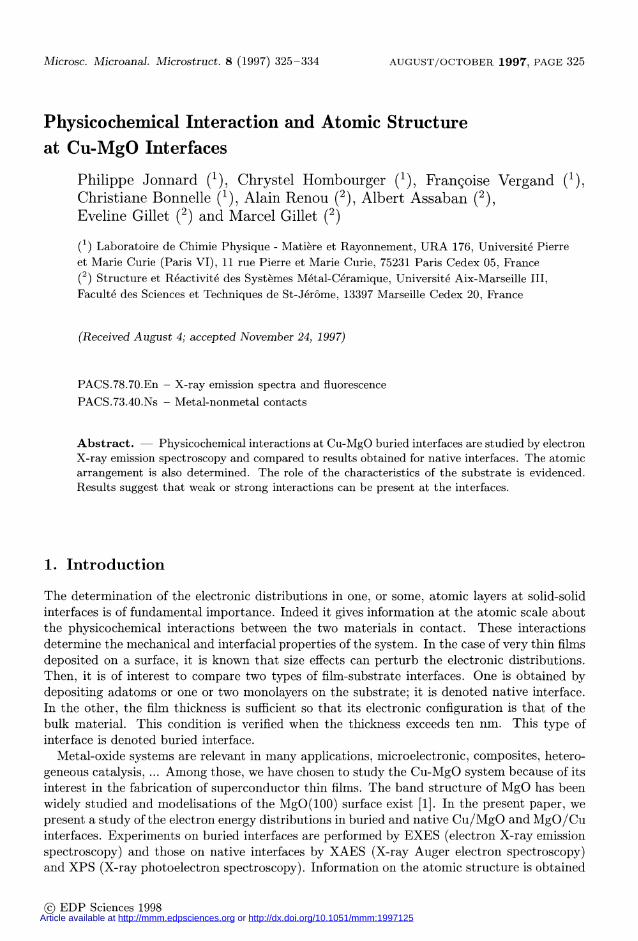
The morphology and the composition of MgO (001) surfaces obtained by cleavage were studiedby AFM in contact mode and also secondary ion mass spectrometry (SIMS). The surfacesappear atomically smooth on large areas, with a mosaïc structure typical of MgO (Fig. 1).
327
Fig. 1. - AFM image of a MgO (100) cleavage showing the mosaïc stucture of the crystal.
SIMS analyzes evidence CH4 and OH ligands which can be removed by annealing under UHV(typically 850 K, 1 h) if the sample is quickly introduced under vacuum after cleavage [5].A Knudsen cell is employed as Cu source. The metal atom flux is calibrated by a quartz
balance at a value of 0.2 nm/min (mass equivalent mean thickness). Metal depositions wereperformed at substrate temperatures in the 300-600 K range. For XPS analyzes of nativeinterfaces, the metal flux was lowered in order to perform sequential deposits.
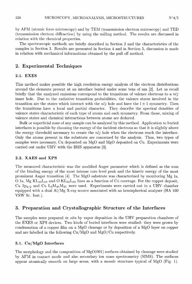
For TEM observations, samples were reduced to powder. The metal films grown at temper-atures lower than 450 K are formed of polycrystalline islands. The surface coverage is achievedfor a Cu deposit mean thickness in the 20 to 30 nm range depending on the substrate annealing.When the temperature deposition exceeds 500 K, a perfect parallel epitaxy takes place withonly one azimutal orientation (OOl)Cu // (OOl)MgO and (100)Cu // (100)MgO, as shown inFigures 2a, b.
The EXES results were obtained from three Cu/MgO (001) interfaces. For the first one,noted Cu/MgO(l), a 10 nm thick Cu film was deposited at 300 K on the air cleaved surface.X-ray diffraction analysis has shown that coherent diffraction domains are larger than 10 nmand microdistorsions are weak [6]. For the second, noted Cu/MgO(2), 20 nm of copper weredeposited at 300 K on a substrate annealed one hour at 750 K. For the last sample, notedCu/MgO(3), a 20 nm thick Cu film was deposited at 520 K on a same substrate.
Adhesion tests were done by the pull off method on samples prepared at different tem-peratures. In the 300-600 K range, the adhesion force increases from 2.6 x 10⁶ N/m2 to8.2 x 106 N/m2 [7].
328
Fig. 2. - a) Electron diffraction pattern obtained by transmission at 100 kV on a Cu/MgO interface.The parallel epitaxy between the metal layer and the oxide is perfect. Double diffraction spots are
present, they correspond to moiré fringes in the micrography. b) Electron micrography (x 170 000) :the layer is continuous and the moirés fringes attest the good quality of the film.
3.2. MgO/Cu Interfaces
MgO/Cu/MgO samples were prepared by deposition of 40 nm of Cu between two MgO layerssupported on a NaCl (100) cleavage. Continuous films of MgO were obtained by vapor deposi-tion from an electron bombardment source. The whole film has a thickness of 80 nm; it can be
observed in TEM after dissolution of NaCl in water. The superficial MgO layer protects themetal against oxidation during the air transfer of the samples towards the analysis chambers.
If the deposition temperatures for MgO and Cu are 400 K and 500 K respectively, the threelayers are oriented on NaCl with the relationships:
(OOl)Cu // (OOl)NaCl and (100)Cu // (100)NaCl(OOl)MgO // (001)Cu and (100)MgO // (100)Cu(lll)MgO // (001)Cu and (110)MgO // (110)Cu
with two orthogonal azimuthal orientations.
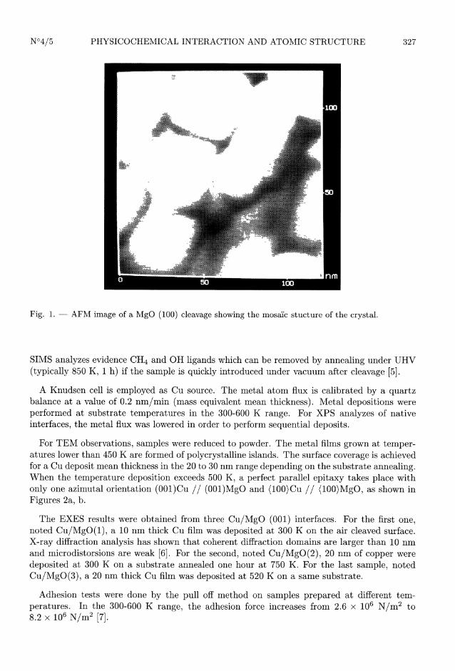
Figures 3a, 3b show TEM micrographies and electron diffraction patterns obtained on thesesamples. Depending on their orientation the MgO films are formed of platelets with square orhexagonal outlines and sizes ranging from 3 to 30 nm. If the deposition temperature of MgOis below 400 K, the sample is polycrystalline with a (001) texture.
Two MgO/Cu interfaces were analyzed by EXES: one with a (001) texture, noted MgO/Cu(l),the other epitaxially oriented, noted MgO/Cu(2).
329
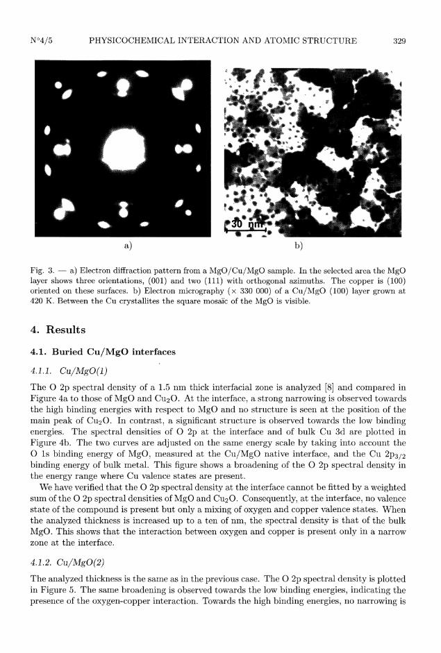
Fig. 3. - a) Electron diffraction pattern from a MgO/Cu/MgO sample. In the selected area the MgOlayer shows three orientations, (001) and two (111) with orthogonal azimuths. The copper is (100)oriented on these surfaces. b) Electron micrography (x 330 000) of a Cu/MgO (100) layer grown at420 K. Between the Cu crystallites the square mosaïc of the MgO is visible.
4. Results
4.1. Buried Cu/Mg0 interfaces
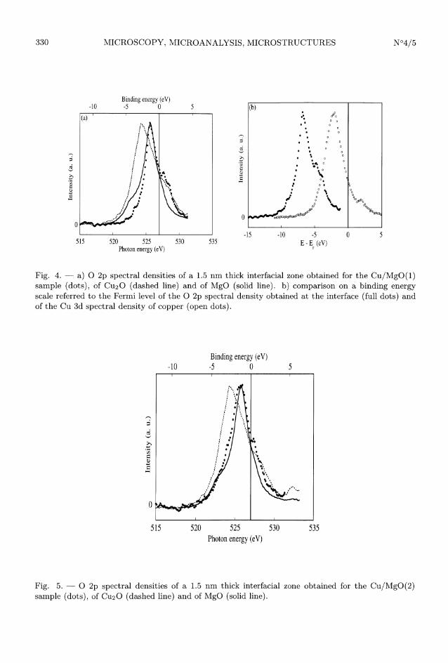
4.1.1. Cu/Mg0 (1)The 0 2p spectral density of a 1.5 nm thick interfacial zone is analyzed [8] and compared inFigure 4a to those of MgO and Cu20. At the interface, a strong narrowing is observed towardsthe high binding energies with respect to MgO and no structure is seen at the position of themain peak of CU20. In contrast, a significant structure is observed towards the low bindingenergies. The spectral densities of 0 2p at the interface and of bulk Cu 3d are plotted inFigure 4b. The two curves are adjusted on the same energy scale by taking into account the0 ls binding energy of MgO, measured at the Cu/MgO native interface, and the Cu 2P3/2binding energy of bulk metal. This figure shows a broadening of the 0 2p spectral density inthe energy range where Cu valence states are present.We have verified that the 0 2p spectral density at the interface cannot be fitted by a weighted
sum of the 0 2p spectral densities of MgO and Cu20. Consequently, at the interface, no valencestate of the compound is present but only a mixing of oxygen and copper valence states. Whenthe analyzed thickness is increased up to a ten of nm, the spectral density is that of the bulkMgO. This shows that the interaction between oxygen and copper is present only in a narrowzone at the interface.
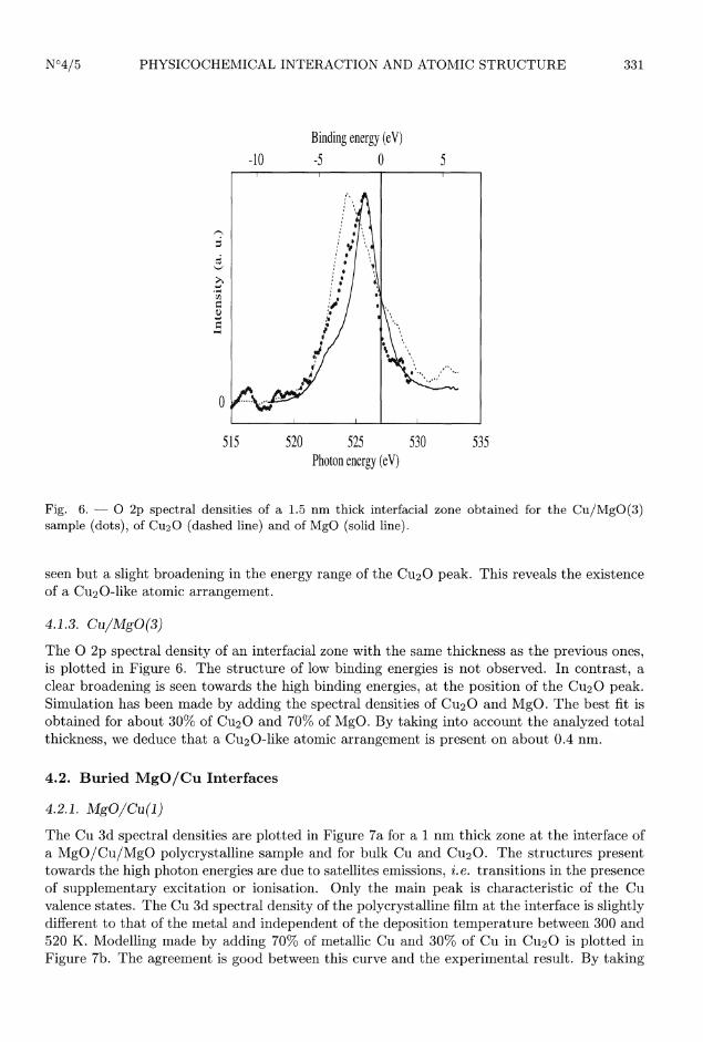
4.1.2. Cu/MgO(2)The analyzed thickness is the same as in the previous case. The 0 2p spectral density is plottedin Figure 5. The same broadening is observed towards the low binding energies, indicating thepresence of the oxygen-copper interaction. Towards the high binding energies, no narrowing is
330
Fig. 4. - a) 0 2p spectral densities of a 1.5 nm thick interfacial zone obtained for the Cu/MgO(l)sample (dots), of Cu20 (dashed line) and of MgO (solid line). b) comparison on a binding energyscale referred to the Fermi level of the 0 2p spectral density obtained at the interface (full dots) andof the Cu 3d spectral density of copper (open dots).
Fig. 5. - 0 2p spectral densities of a 1.5 nm thick interfacial zone obtained for the Cu/MgO(2)sample (dots), of Cu20 (dashed line) and of MgO (solid line).
331
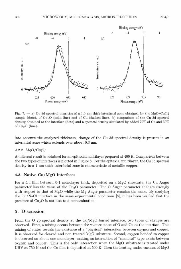
Fig. 6. - 0 2p spectral densities of a 1.5 nm thick interfacial zone obtained for the Cu/MgO(3)sample (dots), of Cu2O (dashed line) and of MgO (solid line).
seen but a slight broadening in the energy range of the Cu20 peak. This reveals the existenceof a Cu20-like atomic arrangement.
4.1.3. Cu/Mg0 (3)The 0 2p spectral density of an interfacial zone with the same thickness as the previous ones,is plotted in Figure 6. The structure of low binding energies is not observed. In contrast, aclear broadening is seen towards the high binding energies, at the position of the Cu2O peak.Simulation has been made by adding the spectral densities of Cu20 and MgO. The best fit isobtained for about 30% of Cu20 and 70% of MgO. By taking into account the analyzed totalthickness, we deduce that a CU20-like atomic arrangement is present on about 0.4 nm.
4.2. Buried MgO/Cu Interfaces
4. 2.1. MgOlCu (1)The Cu 3d spectral densities are plotted in Figure 7a for a 1 nm thick zone at the interface ofa MgO/Cu/MgO polycrystalline sample and for bulk Cu and Cu20. The structures presenttowards the high photon energies are due to satellites emissions, i. e. transitions in the presenceof supplementary excitation or ionisation. Only the main peak is characteristic of the Cuvalence states. The Cu 3d spectral density of the polycrystalline film at the interface is slightlydifferent to that of the metal and independent of the deposition temperature between 300 and520 K. Modelling made by adding 70% of metallic Cu and 30% of Cu in Cu20 is plotted inFigure 7b. The agreement is good between this curve and the experimental result. By taking
332
Fig. 7. - a) Cu 3d spectral densities of a 1.0 nm thick interfacial zone obtained for the MgO/Cu(l)sample (dots), of Cu20 (solid line) and of Cu (dashed line). b) comparison of the Cu 3d spectraldensity obtained at the interface (dots) and a spectral density simulated by added 70% of Cu and 30%ofCu20 (line).
into account the analyzed thickness, change of the Cu 3d spectral density is present in aninterfacial zone which extends over about 0.3 nm.
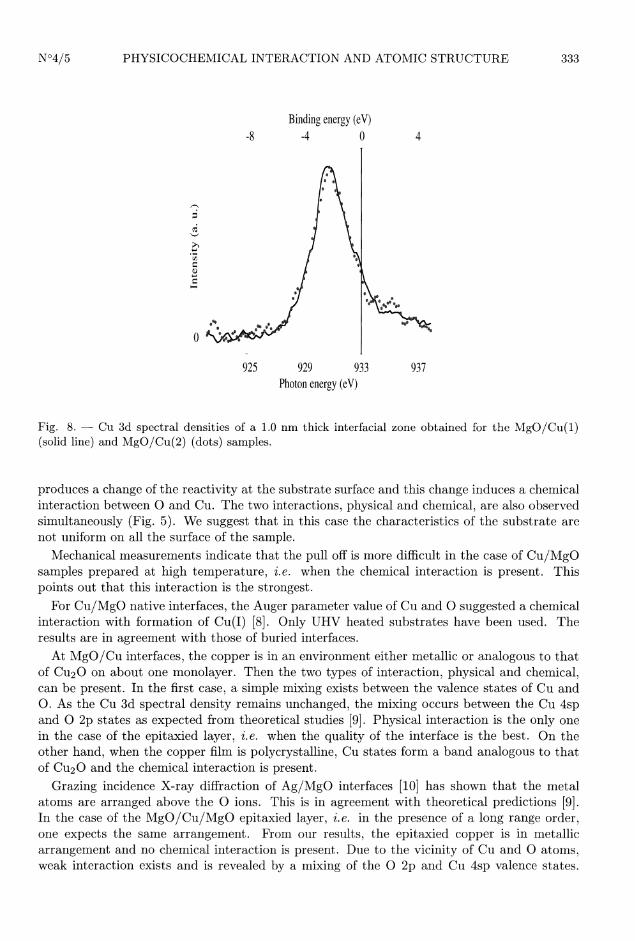
4.2.2. MgO/Cu(2)A different result is obtained for an epitaxial multilayer prepared at 400 K. Comparison betweenthe two types of interfaces is plotted in Figure 8. For the epitaxial multilayer, the Cu 3d spectraldensity in a 1 nm thick interfacial zone is characteristic of metallic copper.
4.3. Native Cu/Mg0 Interfaces
For a Cu film between 0-1 monolayer thick, deposited on a MgO substrate, the Cu Augerparameter has the value of the Cu20 parameter. The 0 Auger parameter changes stronglywith respect to that of MgO while the Mg Auger parameter remains the same. By studyingthe Cu/NaCl interface in the same experimental conditions [8], it has been verified that the
presence of Cu2O is not due to a contamination.
5. Discussion
From the 0 2p spectral density at the Cu/MgO buried interface, two types of changes areobserved. First, a mixing occurs between the valence states of 0 and Cu at the interface. Thismixing of states reveals the existence of a "physical" interaction between oxygen and copper.It is observed for cleaved and non treated MgO substrate. Second, oxygen bonded to copperis observed on about one monolayer, making an interaction of "chemical" type exists betweenoxygen and copper. This is the only interaction when the MgO substrate is treated underUHV at 750 K and the Cu film is deposited at 500 K. Then the heating under vacuum of MgO
333
Fig. 8. - Cu 3d spectral densities of a 1.0 nm thick interfacial zone obtained for the MgO/Cu(l)(solid line) and MgO/Cu(2) (dots) samples.
produces a change of the reactivity at the substrate surface and this change induces a chemicalinteraction between 0 and Cu. The two interactions, physical and chemical, are also observedsimultaneously (Fig. 5). We suggest that in this case the characteristics of the substrate arenot uniform on all the surface of the sample.
Mechanical measurements indicate that the pull off is more difficult in the case of Cu/MgOsamples prepared at high temperature, z.e. when the chemical interaction is present. This
points out that this interaction is the strongest.For Cu/MgO native interfaces, the Auger parameter value of Cu and 0 suggested a chemical
interaction with formation of Cu(I) [8]. Only UHV heated substrates have been used. Theresults are in agreement with those of buried interfaces.At MgO/Cu interfaces, the copper is in an environment either metallic or analogous to that
of Cu20 on about one monolayer. Then the two types of interaction, physical and chemical,can be present. In the first case, a simple mixing exists between the valence states of Cu andO. As the Cu 3d spectral density remains unchanged, the mixing occurs between the Cu 4spand 0 2p states as expected from theoretical studies [9]. Physical interaction is the only onein the case of the epitaxied layer, i. e. when the quality of the interface is the best. On theother hand, when the copper film is polycrystalline, Cu states form a band analogous to thatof Cu20 and the chemical interaction is present.
Grazing incidence X-ray diffraction of Ag/MgO interfaces [10] has shown that the metalatoms are arranged above the 0 ions. This is in agreement with theoretical predictions [9].In the case of the MgO/Cu/MgO epitaxied layer, i. e. in the presence of a long range order,one expects the same arrangement. From our results, the epitaxied copper is in metallic
arrangement and no chemical interaction is present. Due to the vicinity of Cu and 0 atoms,weak interaction exists and is revealed by a mixing of the 0 2p and Cu 4sp valence states.
334
Then the presence of a weak interaction is characteristic of the interface between a noble metaland a perfect MgO surface, in agreement with theoretical predictions [11]. On the other hand,when the deposit is polycrystalline, roughness and disorder are present at the interface andchemical interaction is observed, alone or accompanied by the physical interaction.To conclude, when chemical interaction exists, it is analogous for MgO/Cu and buried and
native Cu/MgO interfaces. A Cu20-like arrangement is thus observed over about one mono-layer. The physical interaction is only seen in the case of the buried interfaces, i. e. when thefilm thicknesses are sufficient so that a tridimensional arrangement could occur. In the case ofthe buried MgO/Cu interface, metallic Cu is observed when a well-ordered arrangement exists.In contrast, for the Cu/MgO interface, the temperature simultaneously changes the atomicarrangement and the reactivity, making different the behaviour of the two inverse interfaces.Then the nature and the characteristics of the substrate play an important role on the existenceof weak or strong interaction at the interface.
Acknowledgments
This work was made within the framework of the GdR-CNRS 1108 "Characterization of inter-faces in multimaterials".
References
[1] Schönberger U. and Aryasetiavan F., Phys. Rev. B 52 (1995) 8788; Ferrari A.M. andPacchioni G., J. Phys. Chem. 99 (1995) 17010; Kantorovich L.N., Holender J.M. andGillan M.J., Surf. Sci. 343 (1995) 221; Birkenhauer U., Boettger J.C. and Rösch N.,J. Chem. Phys. 100 (1994) 6826; Heinrich V.E., The Surface Science of Metal Oxides(Cambridge University Press, 1994); Noguéra C., Goniakowski J. and Bouette-Russo S.,Surf. Sci. 287/288 (1993) 188; Gibson A., Haydock R. and LaFemina J.P., J. Vac. Sci.Technol. A 10 (1992) 2361.
[2] Jonnard P., Vergand F., Staub P.-F., Bonnelle C., Deniau G., Bureau C. and Lecayon G.,Surf. Interface Anal. 24 (1996) 339.
[3] Bonnelle C., Vergand F., Jonnard P., André J.-M., Staub P.-F., Avila P., ChargelègueP., Fontaine M.-F., Laporte D., Paquier P., Ringuenet A. and Rodriguez B., Rev. Sci.Instrum. 65 (1994) 3466.
[4] Moretti G. and Porta P., Surf. Sci. 159 (1990) 16.[5] Yakhloufi M.H.El, Thesis of the University Aix-Marseille III (1993).[6] Badawi K.F., private communication.[7] Assaban A., Colloque National Graines d’Adhésion (Mulhouse, France, 1996).[8] Jonnard P., Hombourger C., Vergand F., Bonnelle C., Ealet B., Renou A. and Gillet E.,
Surf. Rev. Lett. 5 (1998) in press.[9] Li C., Wu R., Freeman A.J. and Fu C., Phys. Rev. B 48 (1993) 8317.
[10] Guénard P., Renaud G. and Villette B., Physica B 221 (1996) 205.[11] Yadunov I., Pacchioni G., Neyman K. and Rösch N., J. Phys. Chem. B 101 (1997) 2786.