Embed Size (px)
Citation preview
Résumés des conférences et affiches

Heure Mercredi 25 Heure Jeudi 26 Heure Vendredi 27
Session 2 9h-12h30
Session 4 9h-12h30
09:00
Tao ZHOU
ESRF 09:00
Anne-Laure BIANCE
ILM
09:45 Anny MICHEL
Institut P’ 09:45 Matthieu BUGNET
MATEIS
10:30 Pause-café 10h30-11h
10:30 Pause-café 10h30-11h
11:00
Thomas JAOUEN
IPR et Univ. Fribourg 11:00
Fabrice COUSIN
LLB
11:45 Jacek
GONIAKOWSKI
INSP
11:45 Véronique VIE
IPR
12:00
Accueil 12h-14h
Hall PNRB
Buffet de
bienvenue 2ème étage
Espace co-working
12:30
Buffet 12h30-14h
2ème étage PNRB
Espace co-working
12:30
Buffet 12h30-14h
2ème étage
Espace co-working
Session 1 14h-18h15
Session 3 14h-16h15
14:00
Xavier MARIE
LPCNO 14:00 Elena SAVINOVA
ICPEES
14:45 Jérôme LAGOUTE
MPQ 14:45 Samy BOUKARI
IPCMS
15:30 Pause-café 15h30-16h
15:30 Mikaël KEPENEKIAN
ISCR
16:00
Christophe BRUN
INSP
16:15
Session Posters 16h15-19h30
16:45 Franck PALMINO
FEMSTO-ST
17:30
Laurence MASSON
CINaM
20:30
Dîner de Gala

Journées Surfaces Interfaces, Rennes 25-27 Janvier 2017
Campus de Beaulieu, Pôle Numérique Rennes Beaulieu (PNRB)
Comité local d'organisation
Sophie GUEZO (IPR)
Jean-Christophe LE BRETON (IPR)
Francine SOLAL (IPR)
Pascal TURBAN (IPR)
Nathalie GICQUIAUX (IPR)
Céline THEBAULT (IPR)
Emmanuelle ROBIN (IPR)
Charles CORNET (FOTON)
Bruno FABRE (ISCR)
Comité Scientifique
Philippe ALLONGUE, PMC, Palaiseau
Pascal ANDREAZZA, ICMN, Orléans
David BABONNEAU, Institut P’, Poitiers
Hervé BULOU, IPCMS, Strasbourg
Alessandro COATI, Synchrotron Soleil, Saint-Aubin
Nicolas COMBE, CEMES, Toulouse
Geneviève GRENET, INL-ECL, Ecully
Sophie GUEZO, IPR, Rennes
Emmanuelle LACAZE, INSP, Paris
Pierre MULLER, CINaM, Marseille
Vincent REPAIN, MPQ, Paris
Nicolas ROUGEMAILLE, Institut Néel, Grenoble
Philippe SONNET, IS2M, Mulhouse


Session 1
Mercredi 25 janvier
14h-18h15

Mercredi 25 janvier 14h
MoS2 et ses Cousins : Nouveaux Matériaux Bidimensionnels
aux Propriétés Prometteuses
Xavier MARIE
Laboratoire de Physique et Chimie des Nano-Objets (UMR 5215)
INSA, 135 Avenue de Rangueil, 31077 Toulouse
Les progrès spectaculaires sur le contrôle des propriétés électroniques du graphène ont
stimulé la recherche de nouveaux matériaux bidimensionnels (2D). Les monocouches de
Dichalcogénures de Métaux de Transition tels que MoS2 (et ses cousins MoSe2, MoTe2, WS2,
WSe2…) sont apparues très récemment comme des nanostructures très prometteuses pour des
applications variées à la fois dans le domaine de l’optique et de l’électronique.
Dans cet exposé, je donnerai un aperçu des propriétés physiques de ces semiconducteurs 2D
(structure de bande, excitons, polarisation de spin/vallée…) et des composants prototypes
(transistor, photodiode, LED ...) basés sur cette nouvelle classe de matériaux.
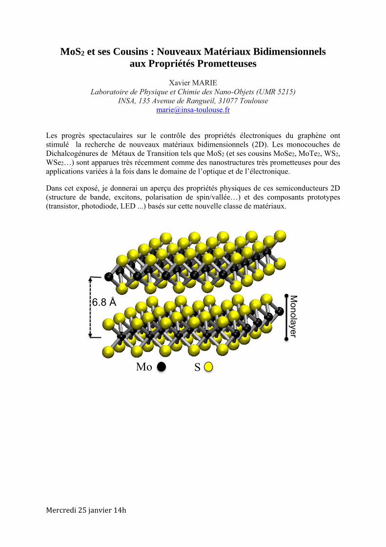
Mo S
Mon
ola
yer
6.8 Å
Mardi 25 janvier 14h45
Dopage du graphène par l’azote mesuré à l’échelle atomique
J. Lagoute1, V. D. Pham1, F. Joucken2, C. Chacon1, V. Repain1, Y. Girard1, A. Bellec1, S.
Rousset1 1 Laboratoire Matériaux et Phénomènes Quantiques, CNRS-Université Paris Diderot
2 Département de physique, Université de Namur
E-mail: [email protected]
La modulation des propriétés du graphène est un enjeu important pour envisager
l’utilisation de ce matériau bidimensionnel dans différents domaines comme l’électronique
moléculaire ou l’énergie. Dans ce contexte, l’insertion d’azote dans le réseau carboné est très
étudiée car cela permet de réaliser un dopage de type n avec peu d’effet de relaxation. Pour
comprendre comment ce dopage modifie la structure électronique du graphène et les implications
qui en résultent, la microscopie à effet tunnel (STM) est un outil de choix pour mesurer à l’échelle
atomique la structure électronique du graphène dopé. L’imagerie STM permet d’identifier des
atomes d’azote isolés insérés dans le graphène ainsi que des paires d’azote [1]. La spectroscopie
locale permet de voir comment la densité d’états est modifiée à l’échelle atomique. En particulier,
nous verrons que le dopage induit non seulement un décalage du point de Driac, mais également
la formation d’états résonants localisés autour des atomes d’azote ce qui implique qu’il faut aller
au-delà d’un modèle de bande rigide pour décrire l’effet du dopage.
Le dopage du graphène modifie également sa réactivité chimique. Afin de comprendre
comment l’interaction du graphène avec avec des molécules organiques est modulée par le dopage,
les propriétés électroniques de molécules de porphyrine sur le graphène dopé ont été étudiées (voir
figure 1). Un décalage en énergie du spectre électronique des porphyrines met en évidence une
interaction électronique locale entre les sites dopants du graphène et les molécules adsorbées. [2,3].
Ces effets seront discutés dans le but de appréhender la manière dont le dopage du graphène
modifie ses propriétés électroniques.
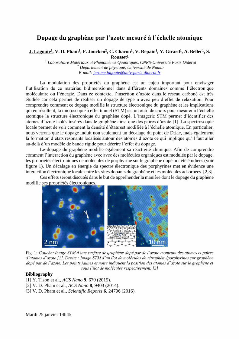
Fig. 1: Gauche: Image STM d’une surface de graphène dopé par de l’azote montrant des atomes et paires
d’atomes d’azote [1]. Droite : Image STM d’un îlot de molécules de tétraphénylporphyrines sur graphène
dopé par de l’azote. Les points jaunes et noirs indiquent la position des atomes d’azote sur le graphène et
sous l’îlot de molécules respectivement. [3]
Bibliography
[1] Y. Tison et al., ACS Nano 9, 670 (2015).
[2] V. D. Pham et al., ACS Nano 8, 9403 (2014).
[3] V. D. Pham et al., Scientific Reports 6, 24796 (2016).
Mercredi 25 janvier 16h
Remarkable superconducting properties of single atomic
layers of lead on silicon
Christophe Brun
Institut des Nanosciences de Paris, CNRS and Université Pierre et Marie Curie,
Paris, France
It is well known that conventional superconductivity is very robust against non-magnetic
disorder [1]. Nevertheless for thin and ultrathin films the structural properties play a major role
in determining the superconducting properties, through a subtle interplay between disorder and
Coulomb interactions [2]. Unexpectedly, in 2010 superconductivity was discovered in single
atomic layers of lead and indium grown on silicon substrate using scanning tunneling
spectroscopy [3] and confirmed later on by macroscopic transport measurements [4]. Such well-
controlled and tunable crystalline monolayers are ideal systems for studying the influence of
various kinds of structural defects on the superconducting properties at the atomic and
mesoscopic scale. In particular, Pb monolayers offer the opportunity of probing new effects of
disorder because not only superconductivity is 2D but also the electronic wave functions are
2D. Our study of two Pb monolayers of different crystal structures by very-low temperature
STM (300 mK) under magnetic field reveals unexpected results involving new spatial
spectroscopic variations [5]. Our results show that although the sheet resistance of the Pb
monolayers is much below the resistance quantum, strong non-BCS corrections appear leading
to peak heights fluctuations in the dI/dV tunneling spectra at a spatial scale much smaller than
the superconducting coherence length. Furthermore, local evidence of the signature of strong
spin-orbit coupling of Rashba type on the superconductivity of the Pb/Si(111) monolayer is
revealed through filling of in gap states and local spatial variations of this filling. Additionally,
the nature of superconducting vortices in a monolayer is found to be very sensitive to the
properties of step edges areas. Finally, we will show that by combining the strong spin-orbit
coupling at play in Pb monolayers grown on Si(111) with magnetic clusters, we should be able
to realize and study 2D topological superconductivity [6,7].
[1] P.W. Anderson, J. Phys. Chem. Solids 11, 26 (1959)
[2] M.V. Feigel'man et al., Ann. Phys. 325, 1390 (2010)
[3] T. Zhang et al., Nature Phys. 6, 104 (2010)
[4] Y. Yamada et al., Phys. Rev. Lett. 110, 237001 (2013)
[5] C. Brun et al., Nature Phys. 444, 10 (2014)
[6] G. Ménard et al. arXiv:1607.06353v1 (2016)
[7] C. Brun, T. Cren and D. Roditchev, Supercond. Sci. Technol. 30, 013003 (2017)
Mercredi 25 janvier 16h45
Molecular self-assembled networks on silicon surface
Palmino Frank, Makoudi Younes, Chérioux Frédéric
Institut FEMTO-ST, Université de Bourgogne Franche-Comté, CNRS, 15B Avenue
des Montboucons, 25030 Besançon cedex, France
E-mail: [email protected]
Nowadays more than 90% of published results show molecules adsorbed onto metallic
or HOPG surfaces. This is explained by the low reactivity between molecules and these
surfaces which induce a molecular diffusion and the possibility to observe large and perfect
self-assemblies. Nevertheless, there are a real economic and technological interests to develop
molecular self-assembled layers onto semiconductors and in particular onto silicon surfaces.
Actually, due to the existence of Si dangling bonds which induce a strong interaction between
molecules and substrates, the formation of such molecular layers is still a real challenge. To
circumvent this problem, we need atomically passivated Si surface. Here, an original
unreactive silicon surface is presented: the high boron doped silicon √3x√3-SiB (111)
reconstruction. Since 10 years, very amazing results have been obtained showing large and
perfect molecular self-assemblies by deposition of home-made and specifically designed
aromatic molecules on this silicon surface [See Fig. 1]. The morphology of each
supramolecular network is explained by the competition between molecule-moleucle and
molecuel-surface interactions [1-4].
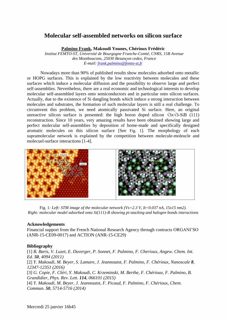
Fig. 1: Left: STM image of the molecular network (Vs=2.3 V, It=0.037 nA, 15x15 nm2).
Right: molecular model adsorbed onto Si(111)-B showing pi-stacking and halogen bonds interactions
Acknowledgements
Financial support from the French National Research Agency through contracts ORGANI’SO
(ANR-15-CE09-0017) and ACTION (ANR-15-CE29)
Bibliography
[1] B. Baris, V. Luzet, E. Duverger, P. Sonnet, F. Palmino, F. Cherioux, Angew. Chem. Int.
Ed. 50, 4094 (2011)
[2] Y. Makoudi, M. Beyer, S. Lamare, J. Jeannoutot, F. Palmino, F. Chérioux, Nanoscale 8,
12347-12351 (2016)
[3] G. Copie, F. Cléri, Y. Makoudi, C. Krzeminski, M. Berthe, F. Chérioux, F. Palmino, B.
Grandidier, Phys. Rev. Lett. 114, 066101 (2015)
[4] Y. Makoudi, M. Beyer, J. Jeannoutot, F. Picaud, F. Palmino, F. Chérioux, Chem.
Commun. 50, 5714-5716 (2014)
Mercredi 25 janvier 17h30
Two-dimensional Si layers on silver substrates
Laurence Masson
Aix Marseille Univ, CNRS, CINaM, Marseille, France E-mail: [email protected]
The large interest in graphene layers and their applications has motivated scientists to
investigate other group-IV two-dimensional (2D) layers that could be graphene's analogous,
i.e. with a honeycomb structure and sp2 bonding. Among these, silicene, a single sheet of
silicon, has aroused considerable interest in the last past five years due to its fundamental
interest [1] and compatibility with Si based-electronics [2]. As solid phase of silicon similar to
graphite does not exist, silicene sheets cannot be synthetized through exfoliation methods as it
was initially done for graphene. One possible route is to grow Si epitaxial sheets on substrates
with expected immiscibility and high commensurability. Pioneering works concern the Si/Ag
system and it has been shown that 2D epitaxial layers can be grown on Ag(110) and Ag(111).
A graphene-like signature in photoemission spectra has been reported on such films,
attributed to the formation of silicene with sp2-sp3 hybridized Si atoms arranged in a 2D
honeycomb lattice [3-5]. However, recent experimental [6-7] and theoretical [8-9] studies
have shown that these conclusions have to be reconsidered. In this talk, it will be shown that
the strong Si-Ag interaction has to be taken into account to interpret the structural, electronic
and optical properties of the Si/Ag interface. Apart from these investigations, 2D Si layers on
Ag(110) can be advantageously used as a template for the self-organized growth of
nanostructures. Recent results concerning the magnetic properties of Co nanolines grown on
Si/Ag(110) studied with X-ray magnetic circular dichroism will be presented [10].
Bibliography
[1] S. Cahangirov, M. Topsakal, E. Aktürk, H. Şahin, S. Ciraci, Phys. Rev. Lett. 102, 236804
(2009).
[2] L. Tao, E. Cinquanta, D. Chiappe, C. Grazianetti, M. Fanciulli, M. Dubey, A. Molle, D.
Akinwande, Nature Nanotech. 10, 227 (2015).
[3] P. De Padova, C. Quaresima, C. Ottaviani, P.M. Sheverdyaeva, P. Moras, C. Carbone, D.
Topwal, B. Olivieri, A. Kara, H. Oughaddou, B. Aufray, G. Le Lay, Appl. Phys. Lett. 96
261905 (2010).
[4] P. Vogt, P. De Padova, C. Quaresima, J. Avila, E. Frantzeskakis, M.C. Asensio, A. Resta,
B. Ealet and G. Le Lay, Phys. Rev. Lett. 108,155501 (2012)
[5] H. Jamgotchian, Y. Colignon, N. Hamzaoui, B. Ealet, J.Y. Hoarau, B. Aufray, and J.P.
Bibérian, J. Phys. Condens. Matter 24 172001 (2012)
[6] R. Bernard, Y. Borensztein, H. Cruguel, M. Lazzeri, G. Prévot, Phys. Rev. B 92, 045415
(2015).
[7] G.Prévot, C. Hogan, T. Leoni, R. Bernard, E. Moyen, L. Masson, Phys. Rev. Lett. accepted
(2016)
[8] S. Cahangirov, M. Audiffred, P. Tang, A. Iacomino, W. Duan, G. Merino and A. Rubio,
Phys. Rev. B 88, 35432 (2013).
[9] P. Gori, O. Pulci, F. Ronci, S. Colonna and F. Bechstedt, J. of Appl. Phys. 114, 113710
(2013).
[10] L. Michez, K. Chen, F. Cheynis, F. Leroy, A. Ranguis, H. Jamgotchian, M. Hanbücken,
L. Masson, Beilstein J. Nanotechnol. 6, 777 (2015).


Session 2
Jeudi 26 janvier
9h-12h30

Jeudi 26 janvier 9h
In situ synchrotron X-ray scattering of SiGe nanowires:
growth, strain and bending
Tao Zhou1, V. Cantelli1, O. Geaymond2, O. Ulrich1, F. Boudaa1, N. Blanc2, P. Müller3
and G. Renaud1 1 Univ. Grenoble Alpes, CEA, INAC/SP2M, F-38000 Grenoble
2 Univ. Grenoble Alpes, CNRS Institut Néel, F-38000 Grenoble
3 Aix-Marseille University CINAM CNRS-UMR 7325, 13288 Marseille
E-mail:: [email protected]
The INS (In situ - Nanostructure - Surface/interface) end station of the BM32
beamline at the European Synchrotron Radiation Facility (ESRF) has been used for years to
analyze the structural properties of nanoparticles in situ, during their growth, combining
Grazing Incidence X-ray Diffraction (GIXD) and Grazing Incidence Small Angle X-ray
Scattering (GISAXS) [1]. An auxiliary UHV-CVD injection system has been recently added
to allow investigations of the VLS and VSS growth of Si/Ge NWs [2].
Results on the growth of Si NWs on Si(111) will first be presented, to demonstrate the
in situ capability of the instrument. The real time NWs length and their size distribution can
be measured with X-ray techniques without removing the sample from the UHV chamber.
The deposition of the metal catalysts and the injection of the precursor gases were carried out
side by side, making it possible to probe the very early stage of growth. The well-known
sidewall dodecagon sawtooth faceting is clearly recognizable from reciprocal space mapping
of both GIXD and GISAXS.
The strain relaxation in Si-Ge core-shell NWs will be presented next. The samples
were kept under UHV during the entire process to avoid oxidation and contamination. The
level of strain was measured in situ as a function of the overgrowth amount. The composition
distribution in the heterostructure was determined using anomalous X-ray scattering, from
which the evolution of the composition during growth was then deduced [3].
Results on the in situ bending of as-grown NWs will also be presented. The bending
was induced, in our case, by depositing a second material on one side of the NWs and was
measured solely by X-ray diffraction techniques. For the quantitative interpretation of the data,
we employ the so-called Displaced Bragg Method (DBM) [4]. The strain profile along the
longitudinal direction of the NWs was obtained by analyzing the position shift of the
displaced Bragg peaks whereas the total stress applied on the NWs was deduced by fitting the
NW curvature, retrieved from integrated intensities of the displaced Bragg peaks, with a
formula based on classic beam theory. Two cases will be presented to illustrate the use and
capability of DBM. We found that the bending induced by Ge deposition on Si NWs sidewall
at 220°C is mainly driven by the misfit stress, which scales almost linearly with Ge film
thickness. On the other hand, the bending induced by the same deposition on Si NWs sidewall
at RT is driven by the surface stress, which evolves from tensile eventually to compressive in
the later stage of Ge growth. Finally, the so-called Stationary Method will be presented,
which allows us to follow in real time, though mostly qualitatively, the entire bending process
in a time efficient manner. The NWs were seen dancing back and forth with increasing
amount of deposition as revealed by live stationary measurements with a 2D detector.
[1] G. Renaud, R. Lazzari, F. Leroy Surf. Sci. Rep. (2009) 64, 255.
[2] V. Cantelli, O. Geaymond, O. Ulrich, T. Zhou, N. Blanc and G. Renaud, submitted.
[3] T. Zhou, O. Geaymond, G. Renaud et al., in preparation.
[4] T. Zhou, O. Robach, G. Renaud et al., in preparation.
Jeudi 26 janvier 9h45
Premiers stades de croissance de films minces métalliques
Anny Michel1, Jonathan Colin1, Clarisse Furgeaud1, Grégory Abadias1, Lionel Simonot1
Bärbel Krause2 (1) D1, Pprime, CNRS - Université de Poitiers – ENSMA, SP2MI, Téléport 2,
Boulevard Marie et Pierre Curie, BP 30179, F86962 Futuroscope-Chasseneuil
(2) IPS, Karlsruhe Institute of Technology (KIT), Allemagne
E-mail: [email protected]
Comprendre le développement de la microstructure et la morphologie de surface
durant la croissance de films minces est d’une importance capitale pour contrôler la texture et
la rugosité des films, mais également la nucléation et la croissance de nanoparticules, la
formation d’îlots, ou les transformations de phase. Ainsi les premiers stades de la croissance
revêtent une grande importance, pour des applications allant des nanoparticules (catalyseurs,
plasmonique) aux composants semiconducteurs de dimensions nanométriques,
La pulvérisation magnétron offre des conditions de dépôt fortement hors-équilibre,
ainsi les aspects cinétiques peuvent prévaloir sur les prédictions thermodynamiques lors de la
croissance. On observe que, sans négliger l’importance des réactions interfaciales, pour des
métaux à forte mobilité, une croissance en îlots est privilégiée alors qu’une croissance
bidimensionnelle sera favorisée à basse mobilité.
En nous situant dans cette problématique, nous avons étudié la croissance de films
minces de différents métaux, sur substrats de silicium oxydé ou sur silicium amorphe, en
privilégiant l’utilisation de techniques de suivi in-situ. Durant la croissance des films, la
mesure optique multi-faisceau de courbure du substrat in-situ et en temps réel est conjuguée à
la spectroscopie de réflectivité différentielle de surface (SDRS), ainsi qu’au suivi en
résistivité électrique, toutes techniques ayant une sensibilité de l’ordre de la monocouche, afin
de relier l’évolution en contrainte des films au mode de croissance adopté. La mesure de
courbure traduit l’évolution de la contrainte dans le film, la SDRS est notamment sensible au
mode de croissance (2D, 3D) par l’identification de résonances de plasmons de surface, tandis
que la résistivité électrique présente une chute brutale lorsque la couche métallique déposée
présente des chemins continus. Nous montrons ici la convergence de ces techniques pour
identifier la croissance en îlots, la percolation puis la continuité du film lors de la croissance
de métaux de forte mobilité (Ag, Cu…).
La croissance de films de basse mobilité est aussi abordée à travers l’étude de la
croissance d’alliages Mo1-xSix. Dans ce cas, une transition de phase amorphe-cristal est mise
en évidence à une épaisseur critique de film déposé, rendant très fructueuse la combinaison de
trois méthodes d’analyse in-situ : la réflectivité X, la diffraction X et le suivi optique des
contraintes. Ces mesures ont été réalisées sur la ligne MPI de la source ANKA (Karlsruhe).
Les résultats démontrent que l’évolution de la contrainte est une traduction directe du
changement de phase. Cette méthodologie unique permet de relier l’épaisseur critique de
cristallisation à la teneur en Si de l’alliage, et par-delà ces résultats l’étude en fonction du
temps de l’épaisseur du film, de sa rugosité et du développement de contraintes donne de
précieuses informations sur la nucléation et la cinétique de formation de la phase cristalline.
Bibliographie
[1] G. Abadias, L. Simonot, J.J. Colin, A. Michel, S. Camelio, D. Babonneau, Appl. Phys. Lett
107, 183105 (2015).
[2] B. Krause, G. Abadias, A. Michel, P. Wochner, S. Ibrahimkutty, T. Baumbach, ACS Appl.
Mater. Interface, DOI: 10.1021/acsami.6b12413 available on line (2016).
Jeudi 26 janvier 11h
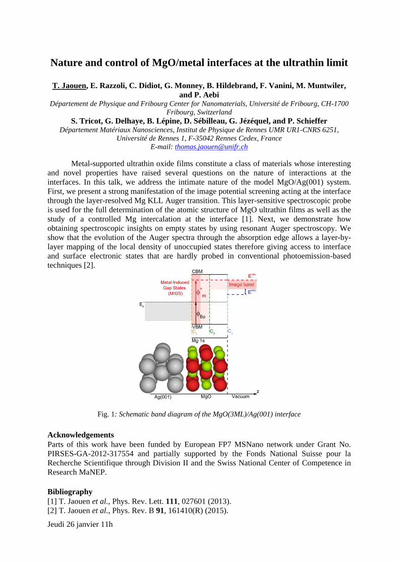
Nature and control of MgO/metal interfaces at the ultrathin limit
T. Jaouen, E. Razzoli, C. Didiot, G. Monney, B. Hildebrand, F. Vanini, M. Muntwiler,
and P. Aebi Département de Physique and Fribourg Center for Nanomaterials, Université de Fribourg, CH-1700
Fribourg, Switzerland
S. Tricot, G. Delhaye, B. Lépine, D. Sébilleau, G. Jézéquel, and P. Schieffer Département Matériaux Nanosciences, Institut de Physique de Rennes UMR UR1-CNRS 6251,
Université de Rennes 1, F-35042 Rennes Cedex, France
E-mail: [email protected]
Metal-supported ultrathin oxide films constitute a class of materials whose interesting
and novel properties have raised several questions on the nature of interactions at the
interfaces. In this talk, we address the intimate nature of the model MgO/Ag(001) system.
First, we present a strong manifestation of the image potential screening acting at the interface
through the layer-resolved Mg KLL Auger transition. This layer-sensitive spectroscopic probe
is used for the full determination of the atomic structure of MgO ultrathin films as well as the
study of a controlled Mg intercalation at the interface [1]. Next, we demonstrate how
obtaining spectroscopic insights on empty states by using resonant Auger spectroscopy. We
show that the evolution of the Auger spectra through the absorption edge allows a layer-by-
layer mapping of the local density of unoccupied states therefore giving access to interface
and surface electronic states that are hardly probed in conventional photoemission-based
techniques [2].
Fig. 1: Schematic band diagram of the MgO(3ML)/Ag(001) interface
Acknowledgements
Parts of this work have been funded by European FP7 MSNano network under Grant No.
PIRSES-GA-2012-317554 and partially supported by the Fonds National Suisse pour la
Recherche Scientifique through Division II and the Swiss National Center of Competence in
Research MaNEP.
Bibliography
[1] T. Jaouen et al., Phys. Rev. Lett. 111, 027601 (2013).
[2] T. Jaouen et al., Phys. Rev. B 91, 161410(R) (2015).
Jeudi 26 janvier 11h45
Nano-polarity: electrostatic effects in free and supported oxide
nano-objects
Jacek Goniakowski and Claudine Noguera
Institut des Nanosciences de Paris
CNRS and Université Pierre et Marie Curie, Paris, France
E-mail: [email protected]
The advances in the fabrication and control of ultra-thin oxide films have fostered the
development of theoretical concepts related to confinement and low dimensionality effects in
these objects. This concerns in particular the electrostatically-driven polarity effects, which
appear to have a sound influence on the stability and properties of ultra-thin films, 2D
ribbons, or nano-islands. Indeed, below a critical size, nano-objects may sustain finite dipole
moments which drive strongly size- and dimensionality- dependent properties. At small sizes,
polarity effects may also extend beyond the surface region and drive structural
transformations of the entire object, resulting in novel structures, with no bulk counterparts.
Finally, since oxide nano-objects are often synthesized on metal substrates, their
characteristics are additionally modified by the electrostatic coupling between their structure
and the interface charge transfer.
Relying on selected examples which were the subject of recent experimental and/or
theoretical works, we will exemplify such novel manifestations of polarity in free and
supported nano-scale oxide films and discuss the consequences for their physico-chemical
properties.
Bibliography
C. Noguera, J. Goniakowski, Chem. Rev. 113, 4073 (2013).
C. Noguera, J. Goniakowski, in Oxide Materials at the Two Dimensional Limit, ed. F.P.
Netzer and A. Fortunelli, Springer Series in Material Science 234, 201, Springer (2016).

Session 3
Jeudi 26 janvier
14h-16h15

Jeudi 26 janvier 14h
Investigation of electrocatalytic materials in operando with Near-
Ambient Pressure XPS (NAP-XPS)
Elena R. Savinova
ICPEES UMR 7515 CNRS-University of Strasbourg,
E-mail: [email protected]
Global pursuit of clean and sustainable energy is guiding the development of
electrochemical energy conversion and storage technologies, including fuel cells, batteries, and
electrolyzers, where the interface between an electronic and an ionic conductor (solid, liquid or
polymer) plays a central role. The development of efficient energy conversion systems not only
requires potent, durable and cost-effective materials, but also asks for precise engineering of
electrochemical interfaces where molecular, ionic and electronic flows merge. Future progress
in the field thus relies heavily on the availability of in situ and in operando techniques to probe
structure and composition of the dynamic electrode/electrolyte interfacial region.
X-ray Photoelectron spectroscopy (XPS) is one of the most powerful techniques for
studies of the chemical composition and the oxidation state of components located within the
near-surface region. Recent advances in vacuum and analyzer technologies have resulted in the
development of specialized instruments which allow performing the so-called Near Ambient
Pressure Photoelectron Spectroscopy (NAP-XPS) measurements in the pressure range of
millibars [1,2].
In this presentation we will discuss recent insights into the structure and dynamics of
electrode/electrolyte interfaces from NAP-XPS measurements of electrocatalytic materials in
operando conditions [3-5]. We will see XPS not only provides information on red-ox transitions
and segregation/dissolution phenomena of the electrode constituents, but also offers insights
into reversible and irreversible electrolyte transformations under polarization [5].
Acknowledgements
This work is partially funded within Grant No. 621237 (INSIDE) of the EU FP7/2007-2013 for
Fuel Cell and Hydrogen Joint Technology Initiative. The author is indebted to all colleagues
who participated in the work.
Bibliography
[1] M. Salmeron, R. Schlögl, Surf. Sci. Rep 63, 169 (2008).
[2] A. Knop-Gericke, E. Kleimenov, M. Hävecker, R. Blume, D. Teschner, S. Zafeiratos, R.
Schlögl, V. I. Bukhtiyarov, V. V. Kaichev, I. P. Prosvirin, A. I. Nizovskii, H. Bluhm, A.
Barinov, P. Dudin, M. Kiskinova, Adv. Catal. 52, 213 (2009).
[3] V. Papaefthimiou, M. Diebold, C. Ulhaq-Bouillet, W. H. Doh, R. Blume, S. Zafeiratos, E.
R. Savinova, ChemElectroChem 2, 1519 (2015).
[4] V. A. Saveleva, L. Wang, W. Luo, S. Zafeiratos, C. Ulhaq-Bouillet, A. S. Gago, K. A.
Friedrich, E. R. Savinova, J.Phys.Chem.Lett. 7, 3240 (2016).
[5] Y. T. Law, S. Zafeiratos, S. G. Neophytides, A. Orfanidi, D. Costa, T. Dintzer, R.
Arrigo, A. Knop-Gericke, R. Schlögl, E. R. Savinova, Chem. Sci. 6, 5635 (2015).
Jeudi 26 janvier 14h45
Interactions between molecules and metals S. Boukari, M. Bowen, M. Alouani, E. Beaurepaire Institut de physique et chimie des matériaux de Strasbourg
23 rue du Loess, 67034 Strasbourg, France
E-mail: [email protected]
To ensure the long-term progress of information technology, radically new concepts,
materials and processing methods are required to circumvent the limitations of traditional
electronics. Spin electronics, or spintronics, adds a new spin degree of freedom to
conventional charge-based electronics. By injecting, transporting, controlling and detecting
spin-polarized currents, new spin-based devices can be obtained, including spin valves
(magnetoresistive devices), spin-FETs (field-effect transistors with spin-polarized source and
drain), spin-LEDs (spin-polarized light-emitting diodes), and quantum bits for quantum
computation and communication.
Separately, organic electronics offers the advantages of low-cost materials and
processing, the tuning of electronic properties by simple chemical routes to build
multifunctional devices, and self-organization. In a more long-term perspective, organic
electronics at the nano- or molecular scale will exploit intriguing electric properties of
nanoscopic objects down to single molecules in electric circuits.
The combination of these two approaches, spin and molecular electronics, gave rise in
the last decade to a new emerging field – termed organic spintronics – that has received
considerable interest since it’s expected to produce devices that could enter in the growing
organic electronics market. Within this field, it appeared that interface properties are
important to understand how devices are working. Indeed, to build a device, molecules will be
chosen a priori on their intrinsic properties. However, once integrated into a device, their
intrinsic properties may change radically. For instance we have shown that phthalocyanine
(Pc) semiconductor molecules turn metallic when adsorbed on cobalt [1], or that the spin
transition of Fe-phenanthroline molecules is precluded when adsorbed on bare Cu(100) but
restored by inserting a CuN layer [2]. The interactions between molecules and metals are not
necessarily deleterious but can be the source of new properties that are hardly predictable. As
an example, Mn-phthalocyanine that present in the bulk no magnetic order above ~9K, can
bias a ferromagnetic Co layer [3]. Therefore, the interactions between molecules and metals is
a fundamental issue for the future of organic spintronics and multifunctional devices.
Bibliography
[1] S. Javaid et al. Phys. Review Lett. 105 077201 (2010).
[2] T. Miyamachi et al. Nat. Commun. 3 938 (2012).
[3] M. Gruber et al. Nature Mater. 14 981 (2015).
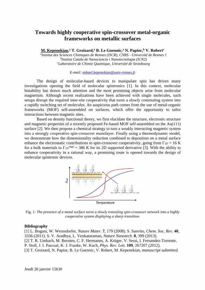
Jeudi 26 janvier 15h30
Towards highly cooperative spin-crossover metal-organic
frameworks on metallic surfaces
M. Kepenekian,a T. Groizard,a B. Le Guennic,a N. Papior,b V. Robertc
aInstitut des Sciences Chimiques de Rennes (ISCR), CNRS - Université de Rennes 1 bInstitut Catala de Nanociencia i Nanotecnologia (ICN2)
cLaboratoire de Chimie Quantique, Université de Strasbourg
E-mail: [email protected]
The design of molecular-based devices to manipulate spin has driven many
investigations opening the field of molecular spintronics [1]. In this context, molecular
bistability has drawn much attention and the most promising objects arise from molecular
magnetism. Although recent realizations have been achieved with single molecules, such
setups disrupt the required inter-site cooperativity that turns a slowly commuting system into
a rapidly switching set of molecules. An auspicious path comes from the use of metal-organic
frameworks (MOF) self-assembled on surfaces, which offer the opportunity to tailor
interactions between magnetic sites.
Based on density functional theory, we first elucidate the structure, electronic structure
and magnetic properties of a recently proposed Fe-based MOF self-assembled on the Au(111)
surface [2]. We then propose a chemical strategy to turn a weakly interacting magnetic system
into a strongly cooperative spin-crossover monolayer. Finally using a thermodynamic model,
we demonstrate how the dimensionality reduction combined to deposition on a metal surface
enhance the electrostatic contributions to spin-crossover cooperativity, going from Γ3D = 16 K
for a bulk materials to Γ2Dsupp = 386 K for its 2D supported derivative [3]. With the ability to
enhance cooperativity in a rational way, a promising route is opened towards the design of
molecular spintronic devices.
Fig. 1: The presence of a metal surface turns a slowly transiting spin-crossover network into a highly
cooperative system displaying a sharp transition.
Bibliography
[1] L. Bogani, W. Wernsdorfer, Nature Mater. 7, 179 (2008). S. Sanvito, Chem. Soc. Rev. 40,
3336 (2011). S. V. Aradhya, L. Venkataraman, Nature Nanotech. 8, 399 (2013).
[2] T. R. Umbach, M. Bernien, C. F. Hermanns, A. Krüger, V. Sessi, I. Fernandez-Torrente,
P. Stoll, J. I. Pascual, K. J. Franke, W. Kuch, Phys. Rev. Lett. 109, 267207 (2012).
[3] T. Groizard, N. Papior, B. Le Guennic, V. Robert, M. Kepenekian, manuscript submitted.


Session 4
Vendredi 27 janvier
9h-12h30

Vendredi 27 janvier 9h
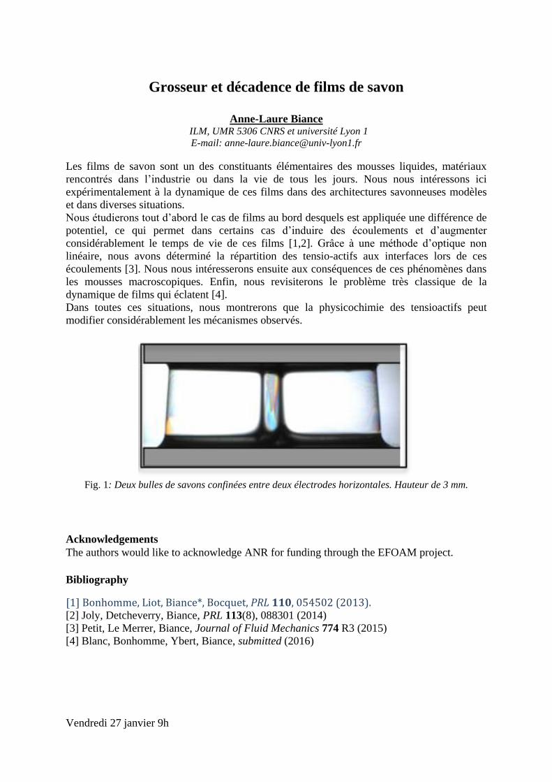
Grosseur et décadence de films de savon
Anne-Laure Biance
ILM, UMR 5306 CNRS et université Lyon 1
E-mail: [email protected]
Les films de savon sont un des constituants élémentaires des mousses liquides, matériaux
rencontrés dans l’industrie ou dans la vie de tous les jours. Nous nous intéressons ici
expérimentalement à la dynamique de ces films dans des architectures savonneuses modèles
et dans diverses situations.
Nous étudierons tout d’abord le cas de films au bord desquels est appliquée une différence de
potentiel, ce qui permet dans certains cas d’induire des écoulements et d’augmenter
considérablement le temps de vie de ces films [1,2]. Grâce à une méthode d’optique non
linéaire, nous avons déterminé la répartition des tensio-actifs aux interfaces lors de ces
écoulements [3]. Nous nous intéresserons ensuite aux conséquences de ces phénomènes dans
les mousses macroscopiques. Enfin, nous revisiterons le problème très classique de la
dynamique de films qui éclatent [4].
Dans toutes ces situations, nous montrerons que la physicochimie des tensioactifs peut
modifier considérablement les mécanismes observés.
Fig. 1: Deux bulles de savons confinées entre deux électrodes horizontales. Hauteur de 3 mm.
Acknowledgements
The authors would like to acknowledge ANR for funding through the EFOAM project.
Bibliography
[1] Bonhomme, Liot, Biance*, Bocquet, PRL 110, 054502 (2013). [2] Joly, Detcheverry, Biance, PRL 113(8), 088301 (2014)
[3] Petit, Le Merrer, Biance, Journal of Fluid Mechanics 774 R3 (2015)
[4] Blanc, Bonhomme, Ybert, Biance, submitted (2016)
Vendredi 27 janvier 9h45
Contributions of environmental TEM to operando surface
analysis
M. Bugnet1*, M. Aouine2, F. J. Cadete Santos Aires2, T. Epicier1,2* 1 Laboratoire MATEIS, UMR 5510 CNRS – Université de Lyon – INSA Lyon 2 Laboratoire IRCELYON, UMR 5256 CNRS – Université de Lyon – UCBL
E-mails: [email protected] (M. B.); [email protected] (T. E.)
Transmission electron microscopy (TEM) is a well-established characterization
technique to combine bulk as well as surface analysis in a wide range of materials at the
nanoscale. Since the large majority of materials are not utilized in moderate or high vacuum,
investigating them in situ in the TEM in more realistic environmental conditions appears
necessary to understand fundamental structural and chemical aspects at surfaces in several
fields of research such as catalysis, corrosion, or crystal growth. In this respect, control of the
nature and the pressure of the atmosphere surrounding the specimen while allowing nanoscale
down to atomic resolution in a transmission electron microscope is of great importance [1, 2].
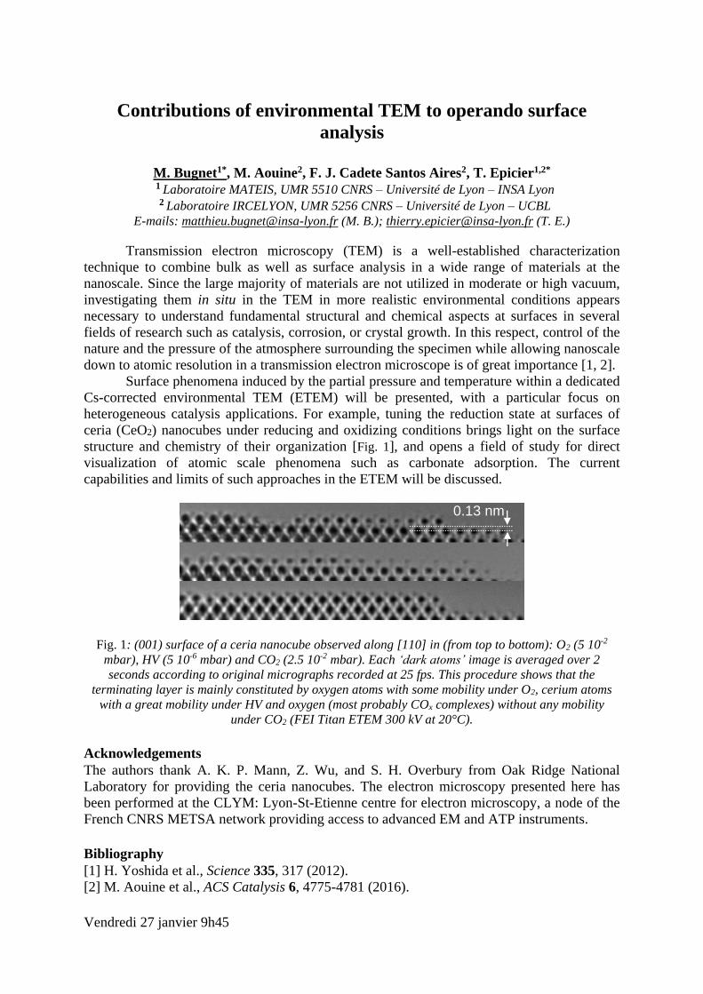
Surface phenomena induced by the partial pressure and temperature within a dedicated
Cs-corrected environmental TEM (ETEM) will be presented, with a particular focus on
heterogeneous catalysis applications. For example, tuning the reduction state at surfaces of
ceria (CeO2) nanocubes under reducing and oxidizing conditions brings light on the surface
structure and chemistry of their organization [Fig. 1], and opens a field of study for direct
visualization of atomic scale phenomena such as carbonate adsorption. The current
capabilities and limits of such approaches in the ETEM will be discussed.
Fig. 1: (001) surface of a ceria nanocube observed along [110] in (from top to bottom): O2 (5 10-2
mbar), HV (5 10-6 mbar) and CO2 (2.5 10-2 mbar). Each ‘dark atoms’ image is averaged over 2
seconds according to original micrographs recorded at 25 fps. This procedure shows that the
terminating layer is mainly constituted by oxygen atoms with some mobility under O2, cerium atoms
with a great mobility under HV and oxygen (most probably COx complexes) without any mobility
under CO2 (FEI Titan ETEM 300 kV at 20°C).
Acknowledgements
The authors thank A. K. P. Mann, Z. Wu, and S. H. Overbury from Oak Ridge National
Laboratory for providing the ceria nanocubes. The electron microscopy presented here has
been performed at the CLYM: Lyon-St-Etienne centre for electron microscopy, a node of the
French CNRS METSA network providing access to advanced EM and ATP instruments.
Bibliography
[1] H. Yoshida et al., Science 335, 317 (2012).
[2] M. Aouine et al., ACS Catalysis 6, 4775-4781 (2016).
0.13 nm
Vendredi 27 janvier 11h
Neutron scattering : a unique tool for probing sot matter systems
at surfaces and interfaces F Cousin1,
Laboratoire Léon Brillouin, CEA-Saclay, 91191 Gif sur Yvette, France
E-mail: [email protected]
“Soft Matter” deals with systems made of individual building blocks (e g colloidal
nanoparticles, polymers, surfactants,) whose characteristic sizes lay in the 0.1–10 nm range.
In such systems, the delicate balance of interactions (of the order of kBT) can lead to the
formation of large self-assembled complex architectures showing specific dynamics, kinetics.
Understanding the underlying mechanisms of their self-assembly and dynamics is then the
key to control and tune their very specific properties at the nanometer scale (1-100 nm). In
this framework, the neutron scattering techniques combined with H/D isotopic labeling are a
unique tool to characterize the systems at the relevant spatial scales of the systems owinf to
the possibilities provided by contrast variation methods.
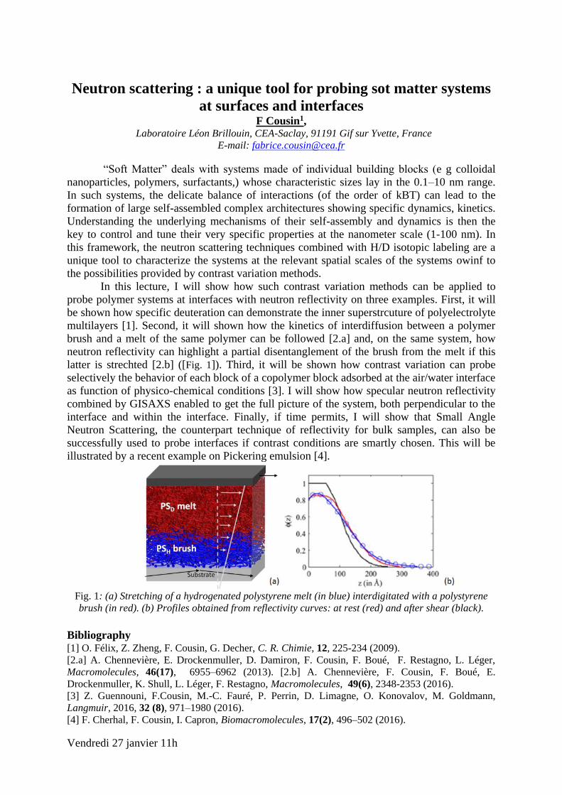
In this lecture, I will show how such contrast variation methods can be applied to
probe polymer systems at interfaces with neutron reflectivity on three examples. First, it will
be shown how specific deuteration can demonstrate the inner superstrcuture of polyelectrolyte
multilayers [1]. Second, it will shown how the kinetics of interdiffusion between a polymer
brush and a melt of the same polymer can be followed [2.a] and, on the same system, how
neutron reflectivity can highlight a partial disentanglement of the brush from the melt if this
latter is strechted [2.b] ([Fig. 1]). Third, it will be shown how contrast variation can probe
selectively the behavior of each block of a copolymer block adsorbed at the air/water interface
as function of physico-chemical conditions [3]. I will show how specular neutron reflectivity
combined by GISAXS enabled to get the full picture of the system, both perpendicular to the
interface and within the interface. Finally, if time permits, I will show that Small Angle
Neutron Scattering, the counterpart technique of reflectivity for bulk samples, can also be
successfully used to probe interfaces if contrast conditions are smartly chosen. This will be
illustrated by a recent example on Pickering emulsion [4].
Fig. 1: (a) Stretching of a hydrogenated polystyrene melt (in blue) interdigitated with a polystyrene
brush (in red). (b) Profiles obtained from reflectivity curves: at rest (red) and after shear (black).
Bibliography [1] O. Félix, Z. Zheng, F. Cousin, G. Decher, C. R. Chimie, 12, 225-234 (2009).
[2.a] A. Chennevière, E. Drockenmuller, D. Damiron, F. Cousin, F. Boué, F. Restagno, L. Léger,
Macromolecules, 46(17), 6955–6962 (2013). [2.b] A. Chennevière, F. Cousin, F. Boué, E.
Drockenmuller, K. Shull, L. Léger, F. Restagno, Macromolecules, 49(6), 2348-2353 (2016).
[3] Z. Guennouni, F.Cousin, M.-C. Fauré, P. Perrin, D. Limagne, O. Konovalov, M. Goldmann,
Langmuir, 2016, 32 (8), 971–1980 (2016).
[4] F. Cherhal, F. Cousin, I. Capron, Biomacromolecules, 17(2), 496–502 (2016).
Vendredi 27 janvier 11h45
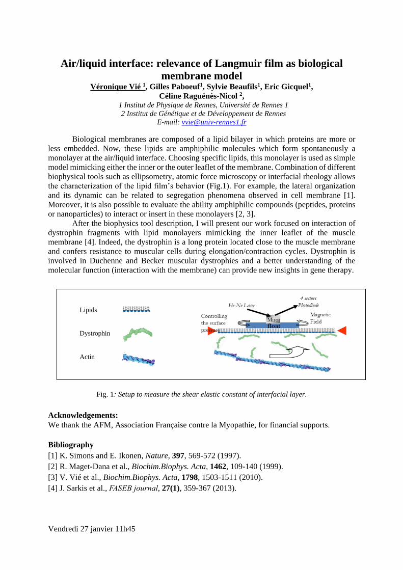
Air/liquid interface: relevance of Langmuir film as biological
membrane model Véronique Vié 1, Gilles Paboeuf1, Sylvie Beaufils1, Eric Gicquel1,
Céline Raguénès-Nicol 2, 1 Institut de Physique de Rennes, Université de Rennes 1
2 Institut de Génétique et de Développement de Rennes
E-mail: [email protected]
Biological membranes are composed of a lipid bilayer in which proteins are more or
less embedded. Now, these lipids are amphiphilic molecules which form spontaneously a
monolayer at the air/liquid interface. Choosing specific lipids, this monolayer is used as simple
model mimicking either the inner or the outer leaflet of the membrane. Combination of different
biophysical tools such as ellipsometry, atomic force microscopy or interfacial rheology allows
the characterization of the lipid film’s behavior (Fig.1). For example, the lateral organization
and its dynamic can be related to segregation phenomena observed in cell membrane [1].
Moreover, it is also possible to evaluate the ability amphiphilic compounds (peptides, proteins
or nanoparticles) to interact or insert in these monolayers [2, 3].
After the biophysics tool description, I will present our work focused on interaction of
dystrophin fragments with lipid monolayers mimicking the inner leaflet of the muscle
membrane [4]. Indeed, the dystrophin is a long protein located close to the muscle membrane
and confers resistance to muscular cells during elongation/contraction cycles. Dystrophin is
involved in Duchenne and Becker muscular dystrophies and a better understanding of the
molecular function (interaction with the membrane) can provide new insights in gene therapy.
Fig. 1: Setup to measure the shear elastic constant of interfacial layer.
Acknowledgements:
We thank the AFM, Association Française contre la Myopathie, for financial supports.
Bibliography
[1] K. Simons and E. Ikonen, Nature, 397, 569-572 (1997).
[2] R. Maget-Dana et al., Biochim.Biophys. Acta, 1462, 109-140 (1999).
[3] V. Vié et al., Biochim.Biophys. Acta, 1798, 1503-1511 (2010).
[4] J. Sarkis et al., FASEB journal, 27(1), 359-367 (2013).
Lipids
Dystrophin
Actin

Session Posters
Jeudi 26 janvier
16h15-19h30

Poster 1
Comparative adsorption study of copper phthalocyanine on
Si(111)(√3 ×√3)R30Ag and Si(111)(√3 ×√3)R30B surfaces
A. Akremi, S. Menzli, C. Chefi
Université de Carthage, Laboratoire de Physique des Matériaux, Unité de Service
Commun Spectromètre de Surfaces, Faculté des Sciences de Bizerte, Jarzouna,
7021 Bizerte, Tunisia
E-mail: [email protected]
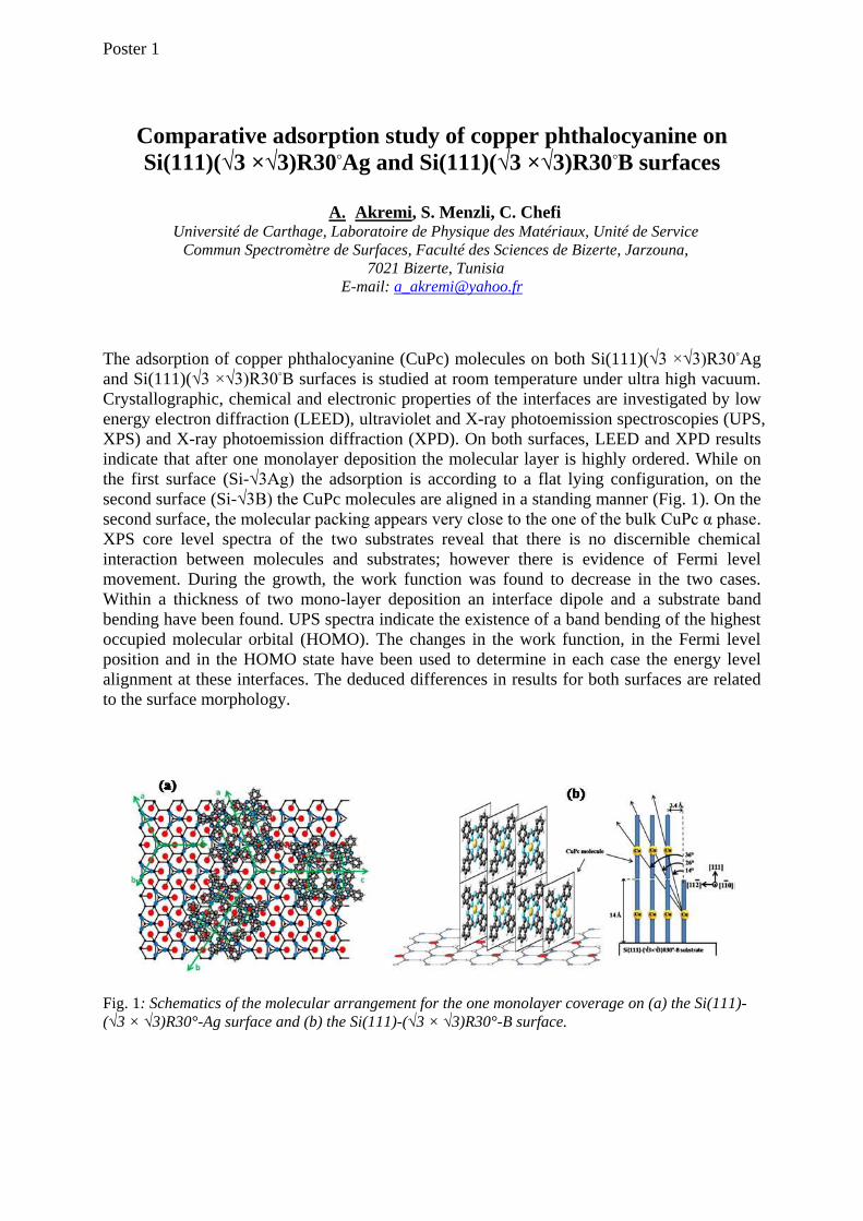
The adsorption of copper phthalocyanine (CuPc) molecules on both Si(111)(√3 ×√3)R30Ag
and Si(111)(√3 ×√3)R30B surfaces is studied at room temperature under ultra high vacuum.
Crystallographic, chemical and electronic properties of the interfaces are investigated by low
energy electron diffraction (LEED), ultraviolet and X-ray photoemission spectroscopies (UPS,
XPS) and X-ray photoemission diffraction (XPD). On both surfaces, LEED and XPD results
indicate that after one monolayer deposition the molecular layer is highly ordered. While on
the first surface (Si-√3Ag) the adsorption is according to a flat lying configuration, on the
second surface (Si-√3B) the CuPc molecules are aligned in a standing manner (Fig. 1). On the
second surface, the molecular packing appears very close to the one of the bulk CuPc α phase.
XPS core level spectra of the two substrates reveal that there is no discernible chemical
interaction between molecules and substrates; however there is evidence of Fermi level
movement. During the growth, the work function was found to decrease in the two cases.
Within a thickness of two mono-layer deposition an interface dipole and a substrate band
bending have been found. UPS spectra indicate the existence of a band bending of the highest
occupied molecular orbital (HOMO). The changes in the work function, in the Fermi level
position and in the HOMO state have been used to determine in each case the energy level
alignment at these interfaces. The deduced differences in results for both surfaces are related
to the surface morphology.
Fig. 1: Schematics of the molecular arrangement for the one monolayer coverage on (a) the Si(111)-
(√3 × √3)R30°-Ag surface and (b) the Si(111)-(√3 × √3)R30°-B surface.
Poster 2
Structure and plasmonic properties of Al nanoparticles
self-aligned in Si3N4 thin films
A. Fafin1,2, F. Pailloux1, S. Camelio1, D. Babonneau1
1Institut Pprime, Département Physique et Mécanique des Matériaux, UPR 3346
CNRS, Université de Poitiers, 86962 Futuroscope Chasseneuil, France 2CEA, LETI, Minatec Campus, 38054 Grenoble, France
E-mail: [email protected]
Aluminum is one of the most promising materials for the future of plasmonics and is
thereby attracting an ever growing attention [1-3]. Indeed, in comparison with the more
traditional plasmonic metals (Ag and Au), the localized surface plasmon resonance (LSPR) of
Al nanoparticles can be tuned from the deep ultraviolet to the near infrared range.
Furthermore, Al nanoparticles show good field enhancement performances. However, Al
nanoparticles are difficult to synthesize and quickly oxidize upon exposure to atmosphere. In
this presentation, we will report on the plasmonic response of Al nanoparticles prepared at
room temperature by glancing-angle ion-beam sputtering deposition onto nanorippled Si3N4
surfaces, and then covered with a transparent Si3N4 capping layer to protect them from
oxidation. Combining energy-filtered transmission electron microscopy (EFTEM) and
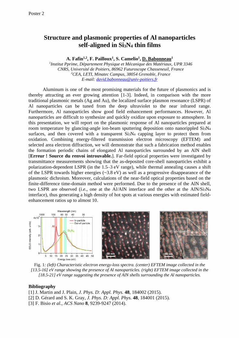
selected area electron diffraction, we will demonstrate that such a fabrication method enables
the formation periodic chains of elongated Al nanoparticles surrounded by an AlN shell
[Erreur ! Source du renvoi introuvable.]. Far-field optical properties were investigated by
transmittance measurements showing that the as-deposited core-shell nanoparticles exhibit a
polarization-dependent LSPR (in the 1.5–3 eV range), while thermal annealing causes a shift
of the LSPR towards higher energies (~3.8 eV) as well as a progressive disappearance of the
plasmonic dichroism. Moreover, calculations of the near-field optical properties based on the
finite-difference time-domain method were performed. Due to the presence of the AlN shell,
two LSPR are observed (i.e., one at the Al/AlN interface and the other at the AlN/Si3N4
interface), thus generating a high density of hot spots at various energies with estimated field-
enhancement ratios up to almost 10.
Fig. 1: (left) Characteristic electron energy-loss spectra. (center) EFTEM image collected in the
[13.5-16] eV range showing the presence of Al nanoparticles. (right) EFTEM image collected in the
[18.5-21] eV range suggesting the presence of AlN shells surrounding the Al nanoparticles.
Bibliography
[1] J. Martin and J. Plain, J. Phys. D: Appl. Phys. 48, 184002 (2015).
[2] D. Gérard and S. K. Gray, J. Phys. D: Appl. Phys. 48, 184001 (2015).
[3] F. Bisio et al., ACS Nano 8, 9239-9247 (2014).
Poster 3
Vectorial method: new method to analyze evolving thin films
BECHU Solène1, FAIRLEY Neal2, FERNANDEZ Vincent1, HUMBERT Bernard1,
RICHARD-PLOUET Mireille1 1. Institut des Matériaux Jean Rouxel, CNRS, University of Nantes, France
2. Casa Software Ltd, Bay House, 5 Grosvenor Terrace, Teignmouth, TQ14 8NE,
United Kingdom
E-mail: [email protected]
Understanding the chemical information at the surface of thin films is a key to predict
the behavior of the material, especially in case the surface evolves under different stimuli. A
hybrid sol-gel1–3 based on titanium oxide has been developed and shows evolution under UV
illumination with the reduction of Ti(IV) to Ti(III) and the apparition of an intermediate band
in its band gap. However, Ti cation is not the only specie impacted by the reduction. To
understand the chemical evolution of those thin films, XPS and Infra-Red measurements were
performed under continuous UV illumination and controlled atmospheres. Information can be
qualitatively extracted from the evolution of spectra but it can be difficult to quantify the
evolution.
The vectorial method4,5 is a method that can, once applied to the set of spectra
generated, provide at least two vectors which will be used to describe the original set of
spectra. Based on CasaXPS software6, this mathematical method generates a weighted
difference from an initial spectrum (before any evolution) to the final one according to the
equation: Xi = (1-ci)So – ciSf, i=1 to 200, with Xi, the vector generated, So and Sf the initial
and final spectra and ci, a coefficient varying from 0 to 1 with an interval of 0.005.
Applied to XPS spectra, this method allows the discovery of a new contribution for
Ti(IV) in Ti 2p spectra, correlated to the appearance of Ti(III) specie under UV illumination.
Applied to Infra-Red spectra, two states of the films, with different organic species, can be
described, corresponding to neutral and photo-reduced states, respectively. The vectors can be
used to describe the whole set of spectra and a percentage of reduction can be extracted. This
percentage is then compared to the one obtained by XPS measurements and shows good
correlation.
Bibliography
[1] Cottineau, T. et al. Chem. Mater. 20, 1421–1430 (2008).
[2] Cottineau, T., Rouet, A., Fernandez, V., Brohan, L. & Richard-Plouet, M. J. Mater.
Chem. A 2, 11499 (2014).
[3] Cottineau, T., Richard-Plouet, M., Mevellec, J.-Y. & Brohan, L. J. Phys. Chem. C 115,
12269–12274 (2011).
[4] Baltrusaitis, J. et al. Appl. Surf. Sci. 326, 151–161 (2015).
[5] d’Halluin, M. et al. Carbon N. Y. 93, 974–983 (2015).
[6] Fairley, N. Casa Software Ltd.
Poster 4
S-segregation anisotropy in Ni grain boundaries:
consequences on embrittlement
I.Braems1
, A. Karpinska1
, D.Connétable2
, P. Ganster3
1 Institut des Matériaux Jean Rouxel (IMN), Université de Nantes, CNRS,
2 rue de la Houssinière, BP 32229, 44322 Nantes cedex 3, France
2CIRIMAT UMR 5085, CNRS-INP-UPS, ENSIACET
4, allée Émile Monso, BP 44362, F-31030 Toulouse Cedex 4, France
3 École de Mines de Saint-Etienne, Centre SMS, Laboratoire Georges Friedel
CNRS-UMR5307, 158 Cours Fauriel, 42023, Saint-Etienne, France
E-mail: [email protected]
Sulphur is one among many non-metallic elements that favor the embrittlement of a
polycristalline nickel sample that is undergoing a tensile test. In the case of the well
documented bicrystal containing the 5(012) grain boundary (GB), atomic-scale
computations revealed a strong segregation of sulphur at the GB [1], that leads to a strong
decrease of both tensile and shear strengths of the bicrystal [2].
However, NanoSIMS experiments showed some years ago that this segregation can
be very different with regards to the GB under investigation. For instance, clean coherent-
twin GBs can coexist with fully segregated other GBs [3]. As such interfaces will not
participate in failure, the description of their interfacial properties (structure, configuration) as
a function of S composition is out of experimental reach via classical techniques such as AES.
We computed the segregation enthalpy and embrittling potencies of one S impurity on
3 different GBs (5(012), 5(013) and the coherent-twin GB 3(111)) using the ReaxFF
potential initally developed by Van Duin et al [2]. For each interface under investigation, the
sign of these quantities respectively indicate if S would segregate at the interface and if it
would participate in embrittling or strengthening the interface. We show that this behaviour is
strongly dependent on the atomic-scale structure of the GB plane. Nevertheless, the
limitations of the ReaxFF potential in describing the segregated interface are also emphasized
and lead to new requirements mostly on the nickel description.
Acknowledgements
This work has been supported by ANR 15 – CE30 – 0016 (GiBBS).
Bibliography
[1] M. Yamaguchi, M. Shiga and H. Kaburaki, Science 307, 393-397 (2005).
[2] H. P. Chen, R.K. Kalia, E. Kaxiras, G. Lu, A. Nakano, K.I. Nomura, A.C.T. Van Duin, P.
Vashishta and Z. Yuan, Physical Review Letters 104, 155502 (2010).
[3] F. Christien, C. Downing, K.L. Moore and C.R.M Grovenor, Surface and Interface
Analysis 3, 377-387.
Poster 5
Physical properties of epitaxial Fe films on SrTiO3 (001)
Pierre Catrou, G. Delhaye, J.-C. Le Breton, S. Tricot, P. Turban, B. Lépine, P. Schieffer
Département Matériaux Nanosciences, Institut de Physique de Rennes UMR UR1-CNRS 6251,
Université de Rennes 1, F-35042 Rennes Cedex, France
E-mail: [email protected]
SrTiO3 is one of the most studied oxides for its own properties and as a substrate for
epitaxial growth of oxides and metals. It has many potential applications in the field of thin
films electronics, in particular memory devices based on a non-volatile resistive switching [1].
In that case, it is important to understand the electronic properties of metal thin films
deposited on SrTiO3. In the field of multiferroic heterostructures, it is also interesting to
compare the well-known Fe/BaTiO3 system to the Fe/SrTiO3 one, in which ferroelectricity
does not exist.
Here we present a detailed study of the electronic and magnetic properties of iron
films deposited on SrTiO3(001) substrates as well as the growth of Fe on this substrate using
x-ray Photoemission Spectroscopy (XPS), Reflection High Energy Electron Diffraction
(RHEED), Atomic Force Microscopy (AFM) and Magneto-Optical Kerr Effect (MOKE). Fe
films from 0.1 nm to 8 nm in thickness were deposited by Molecular Beam Epitaxy (MBE) at
room temperature on Nb-doped and un-doped SrTiO3 (001) substrates. We found that the Fe
films grow with a 45°-rotated cube-on-cube epitaxy on SrTiO3 (001) with a mode close to the
two dimensional mode. The roughness is about 1 nm for an iron thickness of 8 nm. We also
observed that the Fe deposition induces a reduction of the substrate and that only few planes
of TiO2 near the Fe/SrTiO3 interface are implied in this process.
Magnetic properties of Fe films depend on the thickness. The in-plane biaxial
anisotropy constant (>0) decreases linearly with the inverse of thickness. We propose that this
change is linked to the surface in-plane magnetic anisotropy that becomes dominant for the
lowest coverages with a related constant negative.
Finally the Schottky barrier height (SBH) for the Fe/SrTiO3 (001) n-doped junction
was determined from XPS data. We found a value of ~0.2 eV indicating that the contact is
ohmic. Our results disagree with theoretical works which have shown that the SBH for the
Fe/SrTiO3 junctions should be higher than 1.0 eV [2]. The difference between those
theoretical works and our data comes from the fact that the theoretical model does not take
into account the presence of reduced titanium cations at the Fe/SrTiO3 interface.
Acknowledgements
Project funding/reference: Région Bretagne
Bibliography
[1] K. Szot et al. Solid State Physics 65 353 (2014)
[2] M. Mrovec et al. Physical Review B 79 245121 (2009)
Poster 6
Structural and mechanical properties of TiCu metallic glass
thin films deposited by DC and RF magnetron co-sputtering
F. Challali1, A.G. Sanchez1, F. Tétard1, G. Abadias2, L. Belliard3, V. Bockelee1, M.P Besland4,
P. Djemia1 1 LSPM-CNRS, Université Paris 13, Sorbonne Paris-Cité, 99 Avenue J.B. Clément 93430, Villetaneuse, France 2 Département Physique et Mécanique des Matériaux, Institut P’, CNRS-Université de Poitiers-ENSMA, SP2MI -
Téléport 2, BP 30179, F86962 Futuroscope-Chasseneuil, France 3 UPMC-Institut des NanoSciences de Paris, 4 place Jussieu 75252 Paris cedex 05 4 Institut des Matériaux Jean Rouxel – IMN – UMR CNRS 6502, Université de Nantes, 2, rue de la Houssinière, B.P.
32229, 44322, Nantes Cedex 3, France
Corresponding author: [email protected]
Abstract:
Since the first discovery of metallic glasses in 1960 [Klement-1960], researchers have been
interested in their unique atomic structures and their mechanical [Xu-2005, Du-2007], electronic
[Banerjee-2008], and magnetic [Zhang-2000] properties. Simple systems such as binary alloys
either Bulk Metallic Glasses (BMGs) or Thin Films Metallic Glasses (TFMGs) [Chu-2012] are
easily elaborated since a few ten years and their mechanical properties systematically studied
using nanoindentation and µ-compression techniques.
This study focuses on the structural mechanical properties of binary TixCu1-x (TiCu) thin films
metallic glass deposited by magnetron co-sputtering on silicon substrate from Ti and Cu targets in
pure Ar DC and RF plasma discharge, respectively. Process parameters such as DC and RF power,
working pressure, substrate temperature were varied and experimental conditions leading to glass
forming ability were identified. Their influence on the film thickness, microstructure, chemical
composition and mechanical properties were investigated. In particular, the structural properties of
the metallic glass were characterized by X-ray Diffraction (XRD) and X-ray Reflectivity (XRR).
Chemical composition was characterized both by Energy Dispersive X-ray Spectroscopy and X-
Ray Photoelectron Spectroscopy (XPS) leading to bulk and surface insights, respectively. Besides,
the picosecond ultrasonics, the Brillouin light scattering and the nanoindentation techniques were
involved to characterize their acoustic, elastic and hardness properties. A synthesis of main results
will be presented.
References [Chu-2012] J. P. Chu, J.S.C. Jang, et al, Thin Solid Films 520, 5097 (2012)
[Du-2007] X.H. Du, J.C. Huang, et al, Appl. Phys. Lett. 91, 131901(2007)
[Klement-1960] W. Klement, R.H. Willens, P. Duwez, Nature 187, 869 (1960)
[Xu-2005] Y.K. Xu, H. Ma, et al, Acta Mater. 53 1857, (2005)
[Zhang-2000] Z.S. Zhang, M. Ding, et al, Phys. D: Appl. Phys. 33, 185(2000)
Poster 7
Scanning tunneling microscopy investigation of GaP MBE growth
on nominal and vicinal Si(001) substrates for optoelectronic
applications
S. Charbonnier1, I. Lucci2, S. Gangopadhyay3, Y. Ping Wang2, T. Rohel2, R. Bernard2, A.
Létoublon2, C. Cornet 2 and P. Turban1
1: IPR, UMR 6251, CNRS-Université de Rennes I, Campus de Beaulieu 35042 Rennes Cedex,
France 2: UMR FOTON, CNRS, INSA Rennes, Rennes, F35708, France 3: Birla Institute of Technology & Science, Pilani, India
Email: [email protected]
The monolithic integration of III-V based optical functions on Si(001) substrates requires suppression
of antiphase disorder in the III-V active region.[1] We present a detailed scanning tunneling microscopy
(STM) study of epitaxial GaP layers grown by molecular beam epitaxy on nominal and vicinal Si(001)
substrates. The surface morphology of GaP films with thickness varying between 3 and 220 nm is
investigated from large scale down to the atomic level. We show that the use of vicinal substrates
presenting bi-atomic steps only promotes anisotropic growth of the dominant polarity at the early
deposition stages, allowing further annihilation of the antiphase boundaries (APB) on 6°-off Si(001)
substrates.[2] From atomically resolved STM images, we also report on the presence of clearly different
terminal GaP facets on nominal and vicinal substrates. These preliminary results give new ideas on the
effect of a controlled substrate miscut on APB formation and annihilation mechanisms. Finally, the
dependence of thick GaP layer’s roughness with various growth parameters (substrate miscut angle,
V/III flux ratio during growth[3]) is also presented and analyzed.
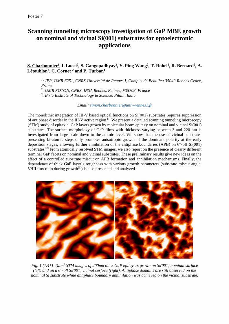
Fig. 1 (1.4*1.4)m2 STM images of 200nm thick GaP epilayers grown on Si(001) nominal surface
(left) and on a 6°-off Si(001) vicinal surface (right). Antiphase domains are still observed on the
nominal Si substrate while antiphase boundary annihilation was achieved on the vicinal substrate.
Poster 7
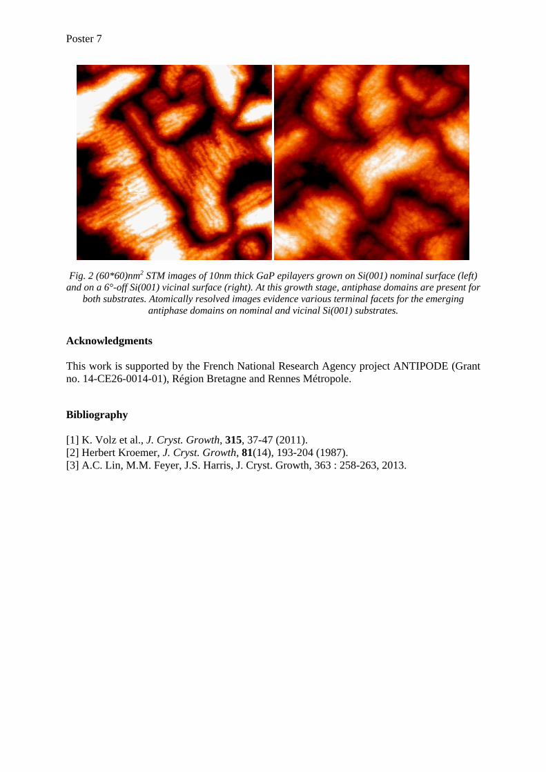
Fig. 2 (60*60)nm2 STM images of 10nm thick GaP epilayers grown on Si(001) nominal surface (left)
and on a 6°-off Si(001) vicinal surface (right). At this growth stage, antiphase domains are present for
both substrates. Atomically resolved images evidence various terminal facets for the emerging
antiphase domains on nominal and vicinal Si(001) substrates.
Acknowledgments
This work is supported by the French National Research Agency project ANTIPODE (Grant
no. 14-CE26-0014-01), Région Bretagne and Rennes Métropole.
Bibliography
[1] K. Volz et al., J. Cryst. Growth, 315, 37-47 (2011).
[2] Herbert Kroemer, J. Cryst. Growth, 81(14), 193-204 (1987).
[3] A.C. Lin, M.M. Feyer, J.S. Harris, J. Cryst. Growth, 363 : 258-263, 2013.
Poster 8
Effect of a normal stress on the shear-coupled grain boundary
migration
N. Combe1,2, F. Mompiou1,2 and M. Legros1,2
1CEMES, CNRS UPR 8011,
29 rue Jeanne Marvig, 31400 Toulouse , France E-mail: [email protected]
Grain boundary (GB) migration occurs in stressed nanocrystalline materials(grains sizes <100
nm) as an alternative vector of plasticity compared to the usual dislocation activity. The
shear-coupled GB migration, the expected most efficient GB based mechanism, couples the
GB motion to an applied shear stress [1,2]. Stresses on GB in polycrystalline material have
however seldom a unique pure shear component.
The influence of a normal stress on the shear coupled GB migration is investigated in a
copper bicrystal studying the 13 (320) GB. Using molecular dynamic simulation, we
theoretically show that the yield shear stress inducing the GB migration strongly depends on
the applied normal stress. Moreover, we show that the application of a normal stress may
induce a modification of the observed GB migration mechanism (mode). We evidence the
existence of the $[010]$ GB migration mode, theoretically predicted but never observed. We
characterize this mode both structurally and energetically using the Nudeg Elastic band
Method.
Bibliography
[1] Rajabzadeh, A.; Mompiou, F.; Legros, M. and Combe, N. Phys. Rev. Lett., 110, 265507
(2013)
[2] Combe N.; Mompiou, F.; Legros, M. Phys. Rev. B, 93, 024109 (2016)
Poster 9
Structure And Growth Mechanism Of Single Layer And Multi-
Layer Silicene
A. Curcella,1 R. Bernard,1 Y. Borensztein,1 A.Resta,3 M. Lazzeri2
1Sorbonne Universités, UPMC Univ Paris 06, CNRS-UMR 7588, Institut des NanoSciences de Paris,
F-75005, Paris, France 2Sorbonne Universités, UPMC Univ Paris 06, CNRS-UMR 7590, MNHN, IRD UMR 206, Institut de
Minéralogie, de Physique des Matériaux et de Cosmochimie, F-75005, Paris, France 3Synchrotron SOLEIL, L’Orme des Merisiers Saint-Aubin–BP 48 91192 Gif-sur-Yvette CEDEX
The last years have seen a growing interest in the research and characterization of 2D
materials, due to their interesting and exotic properties. In particular, for free-standing
silicene, the 2D allotrope of silicium, DFT simulations predicts the existence of Dirac cones
in the electronic structure. This makes silicene an appealing candidate for microelectronic
devices. Experimentally, 2D Si arrangements have been reported on several substrates, among
which Ag(111) is by far the most thoroughly studied.
Silver was thought to weakly interact with the Si sheet; however joint experimental studies
and density functional theory (DFT) simulations have shown a non-negligible interaction [1].
The various structures observed are predicted to be buckled honeycomb lattices. The
electronic band structures computed are however far from the one of free-standing silicene
and depend on the precise atomic positions. In order to decouple the Si layer from the Ag
substrate, researchers have tried to synthetize multi-layer silicene. The structure of the films
obtained is however highly controversial. Whereas some claim that it corresponds to silicite, a
graphite analogue for Si, others affirm that it corresponds to diamond-like Si covered with
Ag.
Combining grazing incidence X-ray diffraction (GIXD) and DFT simulations we managed
to give an accurate structure model of the (4x4) reconstruction of silicene on Ag(111), putting
in evidence the role of the substrate relaxation[3]. The silicene layer shows a buckling of 0.76
Å and the relaxation of the substrate results in a vertical displacement of the Ag atoms at the
interface layer of about 0.25 Å. The relaxation decreases exponentially in the layers deeper
beneath the surface.
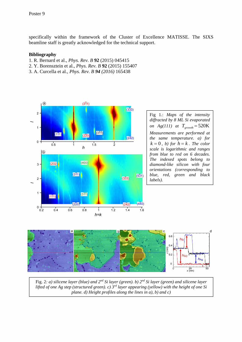
Regarding the synthesis of multi-layer silicene, we have performed real-time GIXD and
scanning tunneling microscopy (STM) during Si evaporation. Diffraction results demonstrate
that the film has a diamond-like structure, Fig. 1, with a large density of stacking faults.
Comparing the experimental structure factors with the theoretical ones obtained from models
known in the literature, we conclude that the surface is terminated with the ( x )
Ag/Si(111) reconstruction, showing the surfactant behavior of Ag atoms in the growth of
Si/Ag(111). This behavior is also confirmed by real-time STM. Moreover, as for the single
layer growth [1], the thick film growth is characterized by Si/Ag atomic exchanges. Indeed,
the formation of thick islands terminated with the ( x ) reconstruction Fig 2a-c is
accompanied by the release of Ag atoms that intercalate beneath the remaining silicene layer,
Fig. 2b. This shows that Si islands grow in the Ag bulk.
Acknowledgements
This work was supported by French state funds managed by the ANR within the
Investissements d’Avenir program under Reference No. ANR-11-IDEX-0004-02 and more
Poster 9
specifically within the framework of the Cluster of Excellence MATISSE. The SIXS
beamline staff is greatly acknowledged for the technical support.
Bibliography
1. R. Bernard et al., Phys. Rev. B 92 (2015) 045415
2. Y. Borensztein et al., Phys. Rev. B 92 (2015) 155407
3. A. Curcella et al., Phys. Rev. B 94 (2016) 165438
Fig. 2: a) silicene layer (blue) and 2nd Si layer (green). b) 2nd Si layer (green) and silicene layer
lifted of one Ag step (structured green). c) 3rd layer appearing (yellow) with the height of one Si
plane. d) Height profiles along the lines in a), b) and c)
Fig 1.: Maps of the intensity
diffracted by 8 ML Si evaporated
on Ag(111) at K520growthT
Measurements are performed at
the same temperature. a) for
0k , b) for kh . The color
scale is logarithmic and ranges
from blue to red on 6 decades.
The indexed spots belong to
diamond-like silicon with four
orientations (corresponding to
blue, red, green and black
labels).
Poster 10
Ga on SiO2 as catalyst for nanowire growth:
Investigation by x-ray photoelectron spectroscopy
Louise Fouquat, Xin Guan, José Penuelas, Geneviève Grenet
Institut des Nanotechnologies de Lyon - Université de Lyon, UMR 5270 - CNRS, Ecole Centrale de
Lyon, 36 avenue Guy de Collongue, F-69134 Ecully cedex, France
GaAs nanowires (NWs) are studied in view of applications in optoelectronic and photonic
devices. In our case, GaAs NWs are grown by Molecular Beam Epitaxy using the Vapor-Liquid-Solid
method, using Ga as catalyst (auto-catalyzed growth) in order to avoid Au, which endangers
optoelectronic performances. Typically, this auto-catalyzed growth is performed directly on Si
substrates without any removal of the native oxide [1-2] or on a SiO2 layer previously deposited on
GaAs wafers [3]. This oxide layer is thought to favor droplet formation with enhanced chemical potential
compared to the Si layer. However, despite this strong interest for the Ga/SiO2/Si system, the mechanism
of the droplet formation and the nature of the chemical interaction between the metal and the substrate
is not yet fully understood.
The Ga-Si system is rather different from the Au-Si one. First, unlike gold, gallium is liquid at
low temperature (about 30 °C). Second, the eutectic Ga1-xSix contains a very small amount of silicon:
only 5.10-8 % vs 18.5 % in Au1-xSix eutectic, for bulk materials. Third, Ga can be easily oxidized and
most Ga oxides are stable: for example, thermal and ozone Ga oxides cannot be removed below
582 ± 1 °C and 638 ± 1°C, respectively. However, it has been shown that the removal of native oxides
from GaAs wafers can be obtained at lower temperature by converting stable Ga2O3 to volatile Ga2O by
exposure to Ga metallic flux.
Using atomic force microscopy and X-ray Photoelectron Spectroscopy (XPS) we have studied
the effect of the growth temperature (from 50 °C to 700 °C) on the formation of the Ga droplets, and the
annealing temperature. Our results show that the size and density of Ga droplet can be controlled by the
growth temperature. This initial configuration of the Ga droplets is of special interest as it determines
NWs dimensions and repartition. The evolution of the Si2p, O1s, Ga3d and As3d core levels as a
function of the growth temperature allows for displaying interfacial Ga oxides in association with a
dewetting phenomenon. Finally, the mechanism of formation of pinholes catalyzed by droplets in the
SiO2 film is discussed.
References
[1] Colombo, C., Spirkoska, D., Frimmer, M., Abstreiter, G. & Fontcuberta I Morral, A. Ga-assisted
catalyst-free growth mechanism of GaAs nanowires by molecular beam epitaxy. Phys. Rev. B - Condens.
Matter Mater. Phys. 77, 2–6 (2008).
[2] Jabeen, F., Grillo, V., Rubini, S. & Martelli, F. Self-catalyzed growth of GaAs nanowires on cleaved
Si by molecular beam epitaxy. Nanotechnology 19, 275711 (2008).
[3] Fontcuberta I Morral, A., Colombo, C., Abstreiter, G., Arbiol, J. & Morante, J. R. Nucleation
mechanism of gallium-assisted molecular beam epitaxy growth of gallium arsenide nanowires. Appl.
Phys. Lett. 92, (2008).
Poster 11
C60 Thin Films On Co(0001) : A Structural Study To Understand
Magnetic Properties
Cynthia Fourmentala,b, Yves Garreaua,b, Alessandro Coatia, Amandine Bellecb et
Vincent Repainb aSynchrotron SOLEIL, L’Orme des Merisiers, Saint-Aubin, BP 48, 91192 Gif sur
Yvette Cedex, France bLaboratoire Matériaux et Phénomènes Quantiques, UMR 7162, Université Paris
Diderot, Sorbonne Paris Cité, Bâtiment Condorcet, 10 rue Alice Domon et Léonie
Duquet, F-75205 Paris Cedex 13, France [email protected]
Due to their long spin relaxation time and the possibility to functionalize them at will,
the use of organic materials is a promising way for the development of new spintronic
applications, especially for the realization of vertical spin valves in which the non-magnetic
spacer is made of an organic film. Promising results have already been obtained on C60 based
spin-valve presenting a magneto-resistance at room temperature [Gobbi2011]. But,
Surprisingly, the magnetic properties of thin Cobalt films can be drastically modified by the
deposition of C60 molecules [Bairagi2015]. Thus, it is crucial to understand how the interface
structure affects magnetic properties in order to improve spintronic devices.
To determine the structure of the interface and its link with magnetism, we are
studying the structure of a model sample of C60 thin films on a Co(0001) single crystal by
surface x-ray scattering and scanning tunneling microscopy, two complementary techniques
giving reciprocal and real space information respectively. Ab-initio calculations complete the
panel of tools used for the investigations. Our studies on C60/Co(0001) monolayer structure,
before and after annealing (Fig. 1), evidence a 4x4 reconstruction of the C60 on Cobalt, as
well as an irreversible structural transition in temperature while annealing. We were also
capable of growing a highly crystalline C60 fcc crystal on Co(0001).
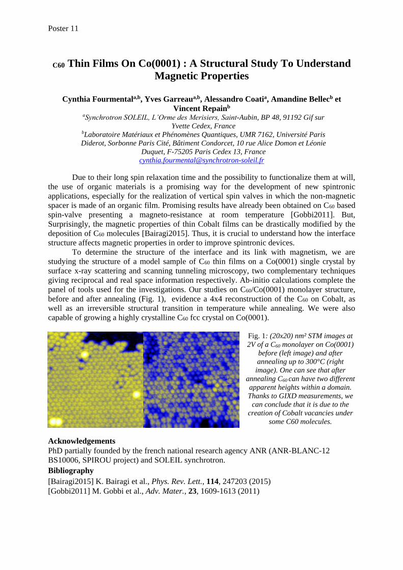
Fig. 1: (20x20) nm² STM images at
2V of a C60 monolayer on Co(0001)
before (left image) and after
annealing up to 300°C (right
image). One can see that after
annealing C60 can have two different
apparent heights within a domain.
Thanks to GIXD measurements, we
can conclude that it is due to the
creation of Cobalt vacancies under
some C60 molecules.
Acknowledgements
PhD partially founded by the french national research agency ANR (ANR-BLANC-12
BS10006, SPIROU project) and SOLEIL synchrotron.
Bibliography
[Bairagi2015] K. Bairagi et al., Phys. Rev. Lett., 114, 247203 (2015)
[Gobbi2011] M. Gobbi et al., Adv. Mater., 23, 1609-1613 (2011)
Poster 12
Photoelectron Energy Loss Spectroscopy :
Retrieval of the Energy Loss Function by a Fourier Transform method
Victor Mancir da Silva Santana1, Denis David1, Christian Godet2
1 Instituto de Fisica, Universidade Federal da Bahia, Campus Universitário de Ondina, 40.210-340
Salvador, Bahia (Brazil)
2 Institut de Physique de Rennes (CNRS UMR 6251), Université Rennes 1, Campus Beaulieu - Bât.
11E, 35042 Rennes (France)
e-mail : [email protected] / [email protected]
Photoelectron Energy Loss Spectroscopy (XPS-PEELS) is a non-destructive tool which
extends analytical capabilities of XPS (chemical composition obtained from core level peak
intensities) to detailed insight in electronic properties (near-surface dielectric function derived
from kinetic energy losses resulting essentially from plasmon excitation).1,2
Using standard spectrometers without monochromatized X-ray source, the intensity measured
over a broad kinetic energy range results from convolution of four spectral distributions: (i)
X-ray source, (ii) Gaussian broadening of photoelectron analyzer, (iii) theoretical
photoemission line shape and (iv) multiple plasmon loss probability. The latter being a self-
convolution of the differential inverse inelastic mean free path, a Fourier transform method is
proposed to retrieve the effective energy loss function and the dielectric function of the solid.
This method is applied to Aluminum single crystal Al(001) where the photoemission line
shape can be computed accurately beyond the Doniach-Sunjic approximation to take into
account the density of states distribution near the Fermi level. Adjustable parameters consist
in broadening energy which results from the core hole lifetime and creation rates for
intrinsic and extrinsic plasmon excitation. After correction for surface plasmon excitations,
the effective dielectric function (, q) of Al(001) differs from the optical limit (, q = 0)
and is well described by the Lindhard and Mermin dispersion relations.
Acknowledgements
Funding and grants: CNPq, Rennes Métropole.
Bibliography
[1] Derivation of the near-surface dielectric function of amorphous silicon from photoelectron loss spectra
D. David et al., J. Non-Cryst. Solids 358, 2019-2022 (2012).
[2] Derivation of dielectric function and inelastic mean free path from photoelectron energy-loss
spectra of amorphous carbon surfaces. D. David et al., Appl. Surf. Sci. 387, 1125-1139 (2016).
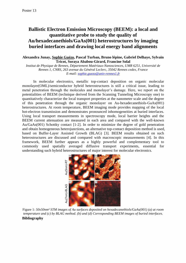
Poster 13
Ballistic Electron Emission Microscopy (BEEM): a local and
quantitative probe to study the quality of
Au/hexadecanethiols/GaAs(001) heterostructures by imaging
buried interfaces and drawing local energy band alignments
Alexandra Junay, Sophie Guézo, Pascal Turban, Bruno lépine, Gabriel Delhaye, Sylvain
Tricot, Soraya Ababou-Girard, Francine Solal Institut de Physique de Rennes, Département Matériaux-Nanosciences, UMR 6251, Université de
Rennes 1, CNRS, 263 avenue du Général Leclerc, 35042 Rennes cedex, France
E-mail: [email protected]
In molecular electronics, metallic top-contact deposition on organic molecular
monolayer(OML)/semiconductor hybrid heterostructures is still a critical issue, leading to
metal penetration through the molecules and monolayer’s damage. Here, we report on the
potentialities of BEEM (technique derived from the Scanning Tunneling Microscopy one) to
quantitatively characterize the local transport properties at the nanometer scale and the degree
of this penetration through the organic monolayer on Au-hexadecanethiols-GaAs(001)
heterostructures. At room temperature, BEEM imaging mode provides mapping of the local
hot-electron transmission and demonstrates pronounced inhomogeneities at buried interfaces.
Using local transport measurements in spectroscopy mode, local barrier heights and the
BEEM current attenuation are measured in each area and compared with the well-known
Au/GaAs(001) Schottky contact [1-2]. In order to minimize the degree of gold penetration
and obtain homogeneous heterojunctions, an alternative top-contact deposition method is used,
based on Buffer-Layer Assisted Growth (BLAG) [3]. BEEM results obtained on such
heterostructures are discussed and compared with macroscopic measurements [4]. In this
framework, BEEM further appears as a highly powerful and complementary tool to
commonly used spatially averaged diffusive transport experiments, essential for
understanding such hybrid heterostructures of major interest for molecular electronics.
Figure 1: 50x50nm² STM images of Au surfaces deposited on hexadecanethiols/GaAs(001) (a) at room
temperature and (c) by BLAG method. (b) and (d) Corresponding BEEM images of buried interfaces.
Bibliography
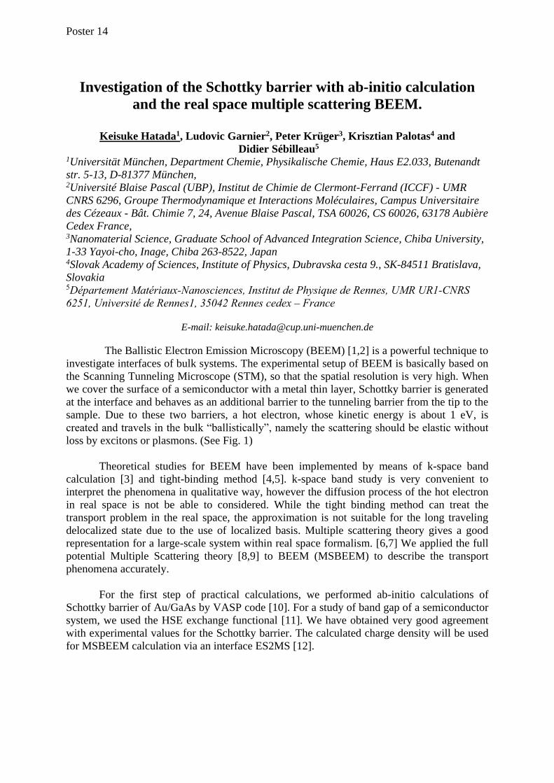
Poster 14
Investigation of the Schottky barrier with ab-initio calculation
and the real space multiple scattering BEEM.
Keisuke Hatada1, Ludovic Garnier2, Peter Krüger3, Krisztian Palotas4 and
Didier Sébilleau5 1Universität München, Department Chemie, Physikalische Chemie, Haus E2.033, Butenandt
str. 5-13, D-81377 München, 2Université Blaise Pascal (UBP), Institut de Chimie de Clermont-Ferrand (ICCF) - UMR
CNRS 6296, Groupe Thermodynamique et Interactions Moléculaires, Campus Universitaire
des Cézeaux - Bât. Chimie 7, 24, Avenue Blaise Pascal, TSA 60026, CS 60026, 63178 Aubière
Cedex France, 3Nanomaterial Science, Graduate School of Advanced Integration Science, Chiba University,
1-33 Yayoi-cho, Inage, Chiba 263-8522, Japan 4Slovak Academy of Sciences, Institute of Physics, Dubravska cesta 9., SK-84511 Bratislava,
Slovakia 5Département Matériaux-Nanosciences, Institut de Physique de Rennes, UMR UR1-CNRS
6251, Université de Rennes1, 35042 Rennes cedex – France
E-mail: [email protected]
The Ballistic Electron Emission Microscopy (BEEM) [1,2] is a powerful technique to
investigate interfaces of bulk systems. The experimental setup of BEEM is basically based on
the Scanning Tunneling Microscope (STM), so that the spatial resolution is very high. When
we cover the surface of a semiconductor with a metal thin layer, Schottky barrier is generated
at the interface and behaves as an additional barrier to the tunneling barrier from the tip to the
sample. Due to these two barriers, a hot electron, whose kinetic energy is about 1 eV, is
created and travels in the bulk “ballistically”, namely the scattering should be elastic without
loss by excitons or plasmons. (See Fig. 1)
Theoretical studies for BEEM have been implemented by means of k-space band
calculation [3] and tight-binding method [4,5]. k-space band study is very convenient to
interpret the phenomena in qualitative way, however the diffusion process of the hot electron
in real space is not be able to considered. While the tight binding method can treat the
transport problem in the real space, the approximation is not suitable for the long traveling
delocalized state due to the use of localized basis. Multiple scattering theory gives a good
representation for a large-scale system within real space formalism. [6,7] We applied the full
potential Multiple Scattering theory [8,9] to BEEM (MSBEEM) to describe the transport
phenomena accurately.
For the first step of practical calculations, we performed ab-initio calculations of
Schottky barrier of Au/GaAs by VASP code [10]. For a study of band gap of a semiconductor
system, we used the HSE exchange functional [11]. We have obtained very good agreement
with experimental values for the Schottky barrier. The calculated charge density will be used
for MSBEEM calculation via an interface ES2MS [12].
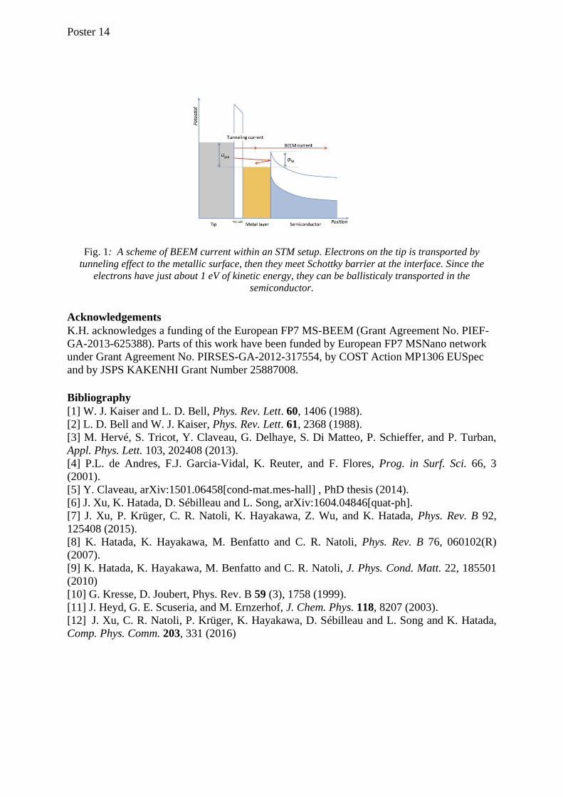
Poster 14
Fig. 1: A scheme of BEEM current within an STM setup. Electrons on the tip is transported by
tunneling effect to the metallic surface, then they meet Schottky barrier at the interface. Since the
electrons have just about 1 eV of kinetic energy, they can be ballisticaly transported in the
semiconductor.
Acknowledgements
K.H. acknowledges a funding of the European FP7 MS-BEEM (Grant Agreement No. PIEF-
GA-2013-625388). Parts of this work have been funded by European FP7 MSNano network
under Grant Agreement No. PIRSES-GA-2012-317554, by COST Action MP1306 EUSpec
and by JSPS KAKENHI Grant Number 25887008.
Bibliography
[1] W. J. Kaiser and L. D. Bell, Phys. Rev. Lett. 60, 1406 (1988).
[2] L. D. Bell and W. J. Kaiser, Phys. Rev. Lett. 61, 2368 (1988).
[3] M. Hervé, S. Tricot, Y. Claveau, G. Delhaye, S. Di Matteo, P. Schieffer, and P. Turban,
Appl. Phys. Lett. 103, 202408 (2013).
[4] P.L. de Andres, F.J. Garcia-Vidal, K. Reuter, and F. Flores, Prog. in Surf. Sci. 66, 3
(2001).
[5] Y. Claveau, arXiv:1501.06458[cond-mat.mes-hall] , PhD thesis (2014).
[6] J. Xu, K. Hatada, D. Sébilleau and L. Song, arXiv:1604.04846[quat-ph].
[7] J. Xu, P. Krüger, C. R. Natoli, K. Hayakawa, Z. Wu, and K. Hatada, Phys. Rev. B 92,
125408 (2015).
[8] K. Hatada, K. Hayakawa, M. Benfatto and C. R. Natoli, Phys. Rev. B 76, 060102(R)
(2007).
[9] K. Hatada, K. Hayakawa, M. Benfatto and C. R. Natoli, J. Phys. Cond. Matt. 22, 185501
(2010)
[10] G. Kresse, D. Joubert, Phys. Rev. B 59 (3), 1758 (1999).
[11] J. Heyd, G. E. Scuseria, and M. Ernzerhof, J. Chem. Phys. 118, 8207 (2003).
[12] J. Xu, C. R. Natoli, P. Krüger, K. Hayakawa, D. Sébilleau and L. Song and K. Hatada,
Comp. Phys. Comm. 203, 331 (2016)
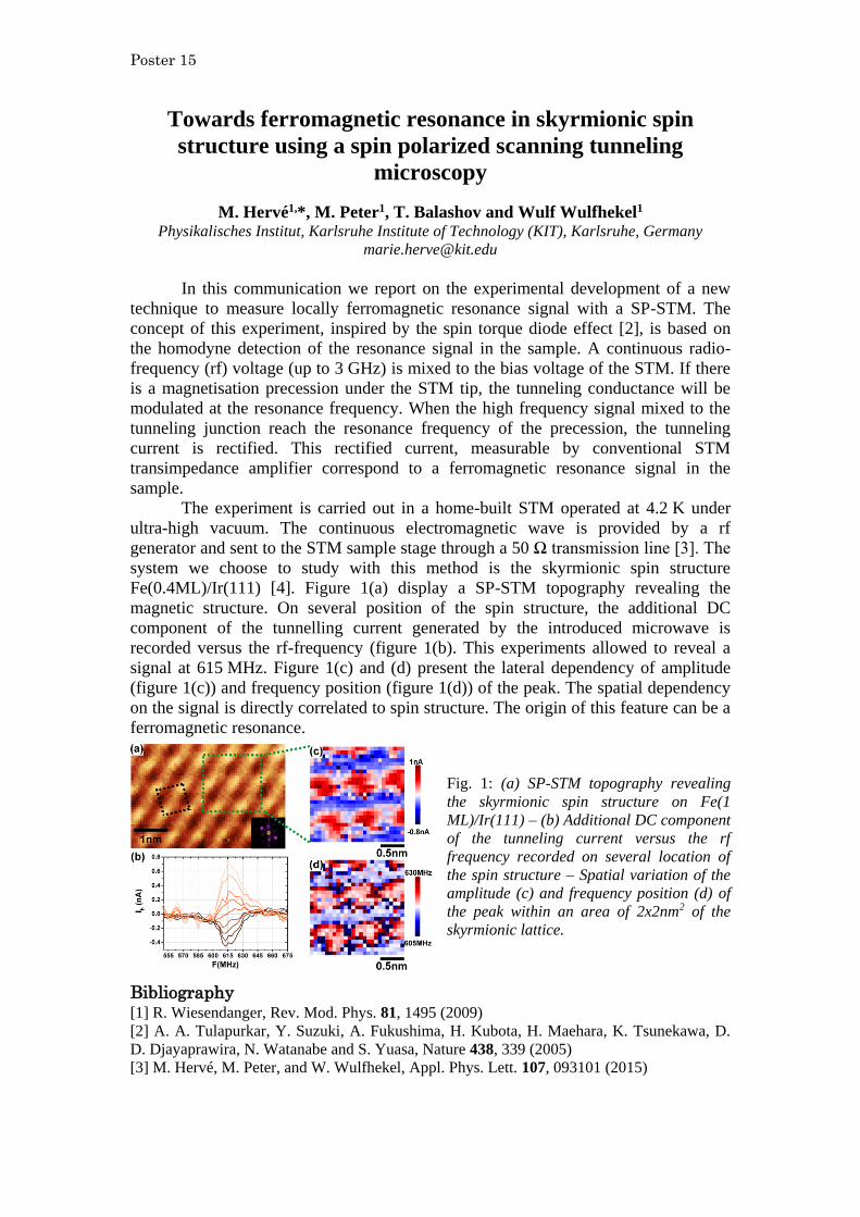
Poster 15
Towards ferromagnetic resonance in skyrmionic spin
structure using a spin polarized scanning tunneling
microscopy
M. Hervé1,*, M. Peter1, T. Balashov and Wulf Wulfhekel1
Physikalisches Institut, Karlsruhe Institute of Technology (KIT), Karlsruhe, Germany
In this communication we report on the experimental development of a new
technique to measure locally ferromagnetic resonance signal with a SP-STM. The
concept of this experiment, inspired by the spin torque diode effect [2], is based on
the homodyne detection of the resonance signal in the sample. A continuous radio-
frequency (rf) voltage (up to 3 GHz) is mixed to the bias voltage of the STM. If there
is a magnetisation precession under the STM tip, the tunneling conductance will be
modulated at the resonance frequency. When the high frequency signal mixed to the
tunneling junction reach the resonance frequency of the precession, the tunneling
current is rectified. This rectified current, measurable by conventional STM
transimpedance amplifier correspond to a ferromagnetic resonance signal in the
sample.
The experiment is carried out in a home-built STM operated at 4.2 K under
ultra-high vacuum. The continuous electromagnetic wave is provided by a rf
generator and sent to the STM sample stage through a 50 Ω transmission line [3]. The
system we choose to study with this method is the skyrmionic spin structure
Fe(0.4ML)/Ir(111) [4]. Figure 1(a) display a SP-STM topography revealing the
magnetic structure. On several position of the spin structure, the additional DC
component of the tunnelling current generated by the introduced microwave is
recorded versus the rf-frequency (figure 1(b). This experiments allowed to reveal a
signal at 615 MHz. Figure 1(c) and (d) present the lateral dependency of amplitude
(figure 1(c)) and frequency position (figure 1(d)) of the peak. The spatial dependency
on the signal is directly correlated to spin structure. The origin of this feature can be a
ferromagnetic resonance.
Fig. 1: (a) SP-STM topography revealing
the skyrmionic spin structure on Fe(1
ML)/Ir(111) – (b) Additional DC component
of the tunneling current versus the rf
frequency recorded on several location of
the spin structure – Spatial variation of the
amplitude (c) and frequency position (d) of
the peak within an area of 2x2nm2 of the
skyrmionic lattice.
Bibliography [1] R. Wiesendanger, Rev. Mod. Phys. 81, 1495 (2009)
[2] A. A. Tulapurkar, Y. Suzuki, A. Fukushima, H. Kubota, H. Maehara, K. Tsunekawa, D.
D. Djayaprawira, N. Watanabe and S. Yuasa, Nature 438, 339 (2005)
[3] M. Hervé, M. Peter, and W. Wulfhekel, Appl. Phys. Lett. 107, 093101 (2015)

Poster 15
[4] S. Heinze, K. von Bergmann, M. Menzel, J. Brede, A. Kubetzka, R. Wiesendanger, G.
Bihlmayer and S. Blügel, Nature Physic 7, 713 (2011)
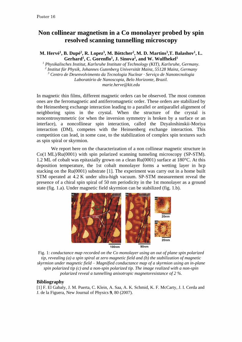
Poster 16
Non collinear magnetism in a Co monolayer probed by spin
resolved scanning tunnelling microscopy
M. Hervé1, B. Dupé2, R. Lopez3, M. Böttcher2, M. D. Martins3,T. Balashov1, L.
Gerhard1, C. Gorenflo1, J. Sinova2, and W. Wulfhekel1 1 Physikalisches Institut, Karlsruhe Institute of Technology (KIT), Karlsruhe, Germany.
2 Institut für Physik, Johannes Gutenberg Universität Mainz, 55128 Mainz, Germany 3 Centro de Desenvolvimento da Tecnologia Nuclear · Serviço de Nanotecnologia
Laboratório de Nanoscopia, Belo Horizonte, Brazil.
In magnetic thin films, different magnetic orders can be observed. The most common
ones are the ferromagnetic and antiferromagnetic order. These orders are stabilized by
the Heinsenberg exchange interaction leading to a parallel or antiparallel alignment of
neighboring spins in the crystal. When the structure of the crystal is
noncentrosymmetric (or when the inversion symmetry is broken by a surface or an
interface), a noncollinear spin interaction, called the Dzyaloshinskii-Moriya
interaction (DM), competes with the Heinsenberg exchange interaction. This
competition can lead, in some case, to the stabilization of complex spin textures such
as spin spiral or skyrmion.
We report here on the characterization of a non collinear magnetic structure in
Co(1 ML)/Ru(0001) with spin polarized scanning tunneling microscopy (SP-STM).
1.2 ML of cobalt was epitaxially grown on a clean Ru(0001) surface at 180°C. At this
deposition temperature, the 1st cobalt monolayer forms a wetting layer in hcp
stacking on the Ru(0001) substrate [1]. The experiment was carry out in a home built
STM operated at 4.2 K under ultra-high vacuum. SP-STM measurement reveal the
presence of a chiral spin spiral of 50 nm periodicity in the 1st monolayer as a ground
state (fig. 1.a). Under magnetic field skyrmion can be stabilized (fig. 1.b).
Fig. 1: conductance map recorded on the Co monolayer using an out of plane spin polarized
tip, revealing (a) a spin spiral at zero magnetic field and (b) the stabilization of magnetic
skyrmion under magnetic field – Magnified conductance map of a skyrmion using an in-plane
spin polarized tip (c) and a non-spin polarized tip. The image realized with a non-spin
polarized reveal a tunnelling anisotropic magnetoresistance of 2 %.
Bibliography [1] F. El Gabaly, J. M. Puerta, C. Klein, A. Saa, A. K. Schmid, K. F. McCarty, J. I. Cerda and
J. de la Figuera, New Journal of Physics 9, 80 (2007).
Poster 17
Photoelectron Diffraction Modeling: Plasmon Effect in Pt and Bi
Vladislav Kochetov1,2, Didier Sébilleau2, Calogero R. Natoli3, Victor Sukhorukov4
and Anna Taranukhina1
1Faculty of Physics, South Federal University, 5 Zorge Street, Rostov on Don,
344090, Russia
2Départment Matériaux-Nanosciences, Institut de Physique de Rennes, UMR UR1-
CNRS 6251, Université de Rennes-1, F-35042 Rennes cedex, France
3INFN Laboratori di Frascati, via E. Fermi 40, C. P. 13, I-00044 Frascati, Italy
4Institute of Physics, South Federal University, 194 Stachky Ave., Rostov on Don,
344090, Russia
E-mail: [email protected]
We report on the multiple scattering modeling of photoelectron diffraction to
investigate two different effects. Photoelectron diffraction is a technique derived from
photoemission which is very much used to characterize the crystallographic structure of
materials. It is generally modeled using a multiple scattering approach [1] . Here, we use the
MsSpec code [2] in order to compute the photoelectron diffraction angular modulations. As is
well-known, these angular variations are strongly dependent of the angular momentum of the
initial state in the low kinetic energy regime while they are initial state-independent for high
kinetic energies [3]. Therefore, we propose first here, to use this effect as a way to reveal the
nature of the experimental feature nearby the 4f core-level peak for Pt and Bi metals which is
supposed to be either 5s or plasmon peak. The probabilities of shake-effects (simultaneous
excitation of 4f-electron and additional electron – 5d, 6s, 6p) were also calculated in the
approximation of sudden perturbations [4].
Acknowledgements
This work has been funded by European FP7 MSNano network under Grant
No. PIRSES-GA-2012-317554
Bibliography
[1] D. Sébilleau, R. Gunnella, Z.-Y. Wu, S. Di Matteo and C. R. Natoli. “Multiple-scattering
approach with complex potential in the interpretation of electron and photon spectroscopies”,
J. Phys.: Condens. Matter 18, R175-R230 (2006)
[2] D. Sébilleau, C. R. Natoli, G. M. Gavaza, H. Zhao, F. Da Pieve and K. Hatada,
“MsSpec-1.0: A multiple scattering package for electron spectroscopies in material science”,
Comp. Phys. Comm. 183, 1567-2579 (2011)
[3] D. Naumović, A. Stuck, T. Greber, J. Osterwalder, and L. Schlapbach. “Full-
hemispherical photoelectron-diffraction data from Cu(001): Energy dependence and
comparison with single-scattering-cluster simulations”, Phys. Rev. B 47, 7462 (1993)
[4] V. P. Sachenko, and V. F. Demekhin, Satellites of X-Ray Spectra Zh. Eksperim. i Teor.
Fiz., 49, 765-769 (1965)
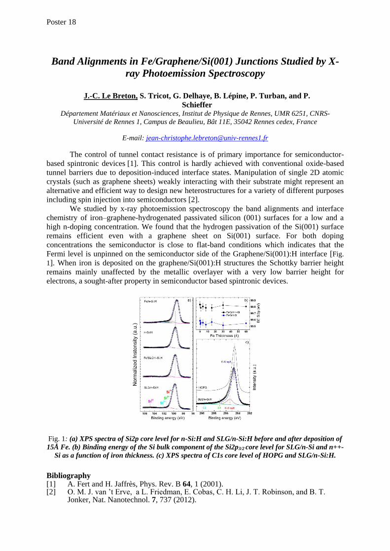
Poster 18
Band Alignments in Fe/Graphene/Si(001) Junctions Studied by X-
ray Photoemission Spectroscopy
J.-C. Le Breton, S. Tricot, G. Delhaye, B. Lépine, P. Turban, and P.
Schieffer
Département Matériaux et Nanosciences, Institut de Physique de Rennes, UMR 6251, CNRS-
Université de Rennes 1, Campus de Beaulieu, Bât 11E, 35042 Rennes cedex, France
E-mail: [email protected]
The control of tunnel contact resistance is of primary importance for semiconductor-
based spintronic devices [1]. This control is hardly achieved with conventional oxide-based
tunnel barriers due to deposition-induced interface states. Manipulation of single 2D atomic
crystals (such as graphene sheets) weakly interacting with their substrate might represent an
alternative and efficient way to design new heterostructures for a variety of different purposes
including spin injection into semiconductors [2].
We studied by x-ray photoemission spectroscopy the band alignments and interface
chemistry of iron–graphene-hydrogenated passivated silicon (001) surfaces for a low and a
high n-doping concentration. We found that the hydrogen passivation of the Si(001) surface
remains efficient even with a graphene sheet on Si(001) surface. For both doping
concentrations the semiconductor is close to flat-band conditions which indicates that the
Fermi level is unpinned on the semiconductor side of the Graphene/Si(001):H interface [Fig.
1]. When iron is deposited on the graphene/Si(001):H structures the Schottky barrier height
remains mainly unaffected by the metallic overlayer with a very low barrier height for
electrons, a sought-after property in semiconductor based spintronic devices.
Fig. 1: (a) XPS spectra of Si2p core level for n-Si:H and SLG/n-Si:H before and after deposition of
15Å Fe. (b) Binding energy of the Si bulk component of the Si2p3/2 core level for SLG/n-Si and n++-
Si as a function of iron thickness. (c) XPS spectra of C1s core level of HOPG and SLG/n-Si:H.
Bibliography [1] A. Fert and H. Jaffrès, Phys. Rev. B 64, 1 (2001). [2] O. M. J. van ’t Erve, a L. Friedman, E. Cobas, C. H. Li, J. T. Robinson, and B. T.
Jonker, Nat. Nanotechnol. 7, 737 (2012).
Poster 19
Effet de la transition de phase structurelle sur la structure
de bande résolue en k de la pérovskite hybride
organique-inorganique CH3NH3PbI3
Min-I Lee∗ , Ana Barragán∗ , Maya Nair†, Vincent Jacques∗ ,
David Le Bolloc’h∗ , Pierre Fertey‡, Khaoula Jemli§,
Ferdinand Lédée , §Gaelle Trippé-Allard ,§Emmanuelle Deleporte§,
Amina Taleb-Ibrahimi†, and Antonio Tejeda∗ ‡
∗Laboratoire de Physique des Solides, CNRS, Univ. Paris-Sud, Universite Paris-Saclay, Bat.
510, 91405 Orsay, France
†UR1 CNRS/Synchrotron SOLEIL, Saint-Aubin, 91192 Gif-sur-Yvette, France
‡Synchrotron SOLEIL, L’Orme des Merisiers, Saint-Aubin, 91192 Gif-sur-Yvette, France
§Laboratoire Aime Cotton, Ecole Normale Superieure de Cachan, CNRS, Universite
Paris-Saclay, Universite Paris-Sud, Bat. 505, 91405 Orsay, France
mailto:[email protected]
Les pérovskites hybrides organiques-inorganiques d'halogénure de plomb sont
devenues des matériaux prometteurs pour le photovoltaïque en raison de leur
rendement élevé de conversion d’énergie solaire, ainsi que de leur fabrication à basse
température et à bas coût en solution.1,2,3 Une des performances la plus remarquables
(22%4) est celle des pérovskites d’halogénure de plomb méthylammonium
(CH3NH3PbI3, MAPI). L’optimisation des performances au-delà nécessiterait d’une
meilleure compréhension de la structure de bande électronique, qui est demeurée
jusqu'à présent difficile à déterminer expérimentale. De plus, l'effet de la transition de
phase structurelle sur la structure de bande dans la plage de température de
fonctionnement des cellules solaires doit être éclairci. Ici, nous présentons la première
détermination expérimentale de la structure de bande de MAPI avec résolution en k.
Nos résultats montrent que la périodicité électronique dans la phase tétragonale de
MAPI (inférieure à 50 ° C) correspond à celle de la phase cubique au haute
température. Cela explique l'insensibilité des cellules solaires dans la gamme
habituelle des températures de fonctionnement malgré la transition structurelle de
tétragonale-cubique.
Acknowledgements
The project leading to this article has received funding from the European Union’s
Poster 19
Horizon 2020 research and innovation program under grant agreement No 687008
(GOTSolar).
Bibliography
[1] Burschka, J., Pellet, N., Moon, S.-J., Humphry-Baker, R., Gao, P., Nazeeruddin,
M.K., & Grätzel, M., Nature 499, 316 (2013).
[2] Jeon, N.J., Noh, J.H., Kim, Y.C., Yang, W.S., Ryu, S., & Seok, S.I., Nature
Materials 13, 897 (2014).
[3] Lee, M. M., Teuscher, J., Miyasaka, T., Murakami, T. N. & Snaith, H. J., Science
338, 643-647 (2012).
[4] Yang WS, Noh JH, Jeon NJ, Kim YC, Ryu S, Seo J, Seok SI., Science 348 (6240),
1234–1237 (2015).
Poster 20
Molecular Magnets: From the single molecule
to the 3D self-assembly
D. Longo1, G. Ménard1, M. Farronato1, S. Royer1, C. Brun1, F. Debontridder1, P. David1
N.Witkowski1, T.Cren1
1 Institut des Nanosciences de Paris, Sorbonne Universités, CNRS UMR 7588 and UPMC, Paris,
France E-mail: [email protected]
Real materials are not pure. Impurities can bring to light beautiful physics: they are
crucial, for instance, in achieving the functionality of doped semiconductors. In general, the
response of a physical system to disorder can lead to elucidating details of its electronic
properties.
In particular, magnetic impurities in superconductors are able to reduce the
superconducting BCS gap and may ultimately destroy the superconducting state. A single
classical spin of a magnetic atom is able to create a localized bound state within the BCS gap
(Shiba state). Consequently, a finite concentration of magnetic impurities can form an
impurity band within the superconducting gap. The spatial decay of these bound states
critically depends on the dimensionality of the system, i.e. it increases by reducing the
dimensionality [1].
The Pb/Si(111) system is one of the most remarkable examples of 2D superconductors
in which superconductivity arises in a single atomic plane of Pb [2,3]. The use of magnetic
phthalocyanines as magnetic impurities, by evaporating them on the Pb monolayer (UHV
conditions), might lead to some advantages. For instance, their self-assembly properties
together with substrate anisotropy allow tailoring both 1D and 2D arrays of magnetic centres
[4]. For this reason, it is very intriguing to investigate the superconducting substrate-mediated
interaction [5] between two Shiba states, which could be used as building block in order to
coherently couple distant magnetic molecules. Such long-range coupling of magnetic
impurities through a 2D superconductor could be an efficient way to create new topological
phases.
Acknowledgements
Project funding/reference
Bibliography
[1] G. Ménard et al. Nature Physics 11, 1013 (2015)
[2] T. Zhang et al. Nature Physics 6, 104 (2010)
[3] C. Brun et al. Nature Physics 10, 444 (2014)
[4] Gargiani et al. Phys. Rev. B 87, 165407 (2013)
[5] Braunecker, et al. Phys. Rev. Lett. 111, 147202 (2013)
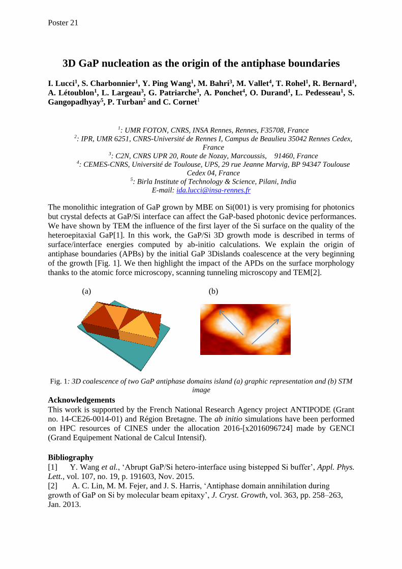
Poster 21
3D GaP nucleation as the origin of the antiphase boundaries
I. Lucci1, S. Charbonnier1, Y. Ping Wang1, M. Bahri3, M. Vallet4, T. Rohel1, R. Bernard1,
A. Létoublon1, L. Largeau3, G. Patriarche3, A. Ponchet4, O. Durand1, L. Pedesseau1, S.
Gangopadhyay5, P. Turban2 and C. Cornet1
1: UMR FOTON, CNRS, INSA Rennes, Rennes, F35708, France
2: IPR, UMR 6251, CNRS-Université de Rennes I, Campus de Beaulieu 35042 Rennes Cedex,
France 3: C2N, CNRS UPR 20, Route de Nozay, Marcoussis, 91460, France
4: CEMES-CNRS, Université de Toulouse, UPS, 29 rue Jeanne Marvig, BP 94347 Toulouse
Cedex 04, France 5: Birla Institute of Technology & Science, Pilani, India
E-mail: [email protected]
The monolithic integration of GaP grown by MBE on Si(001) is very promising for photonics
but crystal defects at GaP/Si interface can affect the GaP-based photonic device performances.
We have shown by TEM the influence of the first layer of the Si surface on the quality of the
heteroepitaxial GaP[1]. In this work, the GaP/Si 3D growth mode is described in terms of
surface/interface energies computed by ab-initio calculations. We explain the origin of
antiphase boundaries (APBs) by the initial GaP 3Dislands coalescence at the very beginning
of the growth [Fig. 1]. We then highlight the impact of the APDs on the surface morphology
thanks to the atomic force microscopy, scanning tunneling microscopy and TEM[2].
(a) (b)
Fig. 1: 3D coalescence of two GaP antiphase domains island (a) graphic representation and (b) STM
image
Acknowledgements
This work is supported by the French National Research Agency project ANTIPODE (Grant
no. 14-CE26-0014-01) and Région Bretagne. The ab initio simulations have been performed
on HPC resources of CINES under the allocation 2016-[x2016096724] made by GENCI
(Grand Equipement National de Calcul Intensif).
Bibliography
[1] Y. Wang et al., ‘Abrupt GaP/Si hetero-interface using bistepped Si buffer’, Appl. Phys.
Lett., vol. 107, no. 19, p. 191603, Nov. 2015.
[2] A. C. Lin, M. M. Fejer, and J. S. Harris, ‘Antiphase domain annihilation during
growth of GaP on Si by molecular beam epitaxy’, J. Cryst. Growth, vol. 363, pp. 258–263,
Jan. 2013.
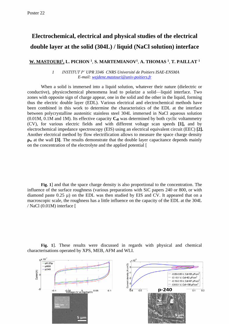
Poster 22
Electrochemical, electrical and physical studies of the electrical
double layer at the solid (304L) / liquid (NaCl solution) interface
W. MASTOURI1, L. PICHON 1, S. MARTEMIANOV1, A. THOMAS 1, T. PAILLAT 1
1 INSTITUT P’ UPR 3346 CNRS Université de Poitiers ISAE-ENSMA
E-mail: [email protected]
When a solid is immersed into a liquid solution, whatever their nature (dielectric or
conductive), physicochemical phenomena lead to polarize a solid—liquid interface. Two
zones with opposite sign of charge appear, one in the solid and the other in the liquid, forming
thus the electric double layer (EDL). Various electrical and electrochemical methods have
been combined in this work to determine the characteristics of the EDL at the interface
between polycrystalline austenitic stainless steel 304L immersed in NaCl aqueous solution
(0.01M, 0.1M and 1M). Its effective capacity Cdl was determined by both cyclic voltammetry
(CV), for various electric fields and with different voltage scan speeds [1], and by
electrochemical impedance spectroscopy (EIS) using an electrical equivalent circuit (EEC) [2].
Another electrical method by flow electrification allows to measure the space charge density
ρw at the wall [3]. The results demonstrate that the double layer capacitance depends mainly
on the concentration of the electrolyte and the applied potential [
Fig. 1] and that the space charge density is also proportional to the concentration. The
influence of the surface roughness (various preparations with SiC papers 240 or 800, or with
diamond paste 0.25 µ) on the EDL was then studied by EIS and CV. It appeared that on a
macroscopic scale, the roughness has a little influence on the capacity of the EDL at the 304L
/ NaCl (0.01M) interface [
Fig. 1]. These results were discussed in regards with physical and chemical
characterisations operated by XPS, MEB, AFM and WLI.
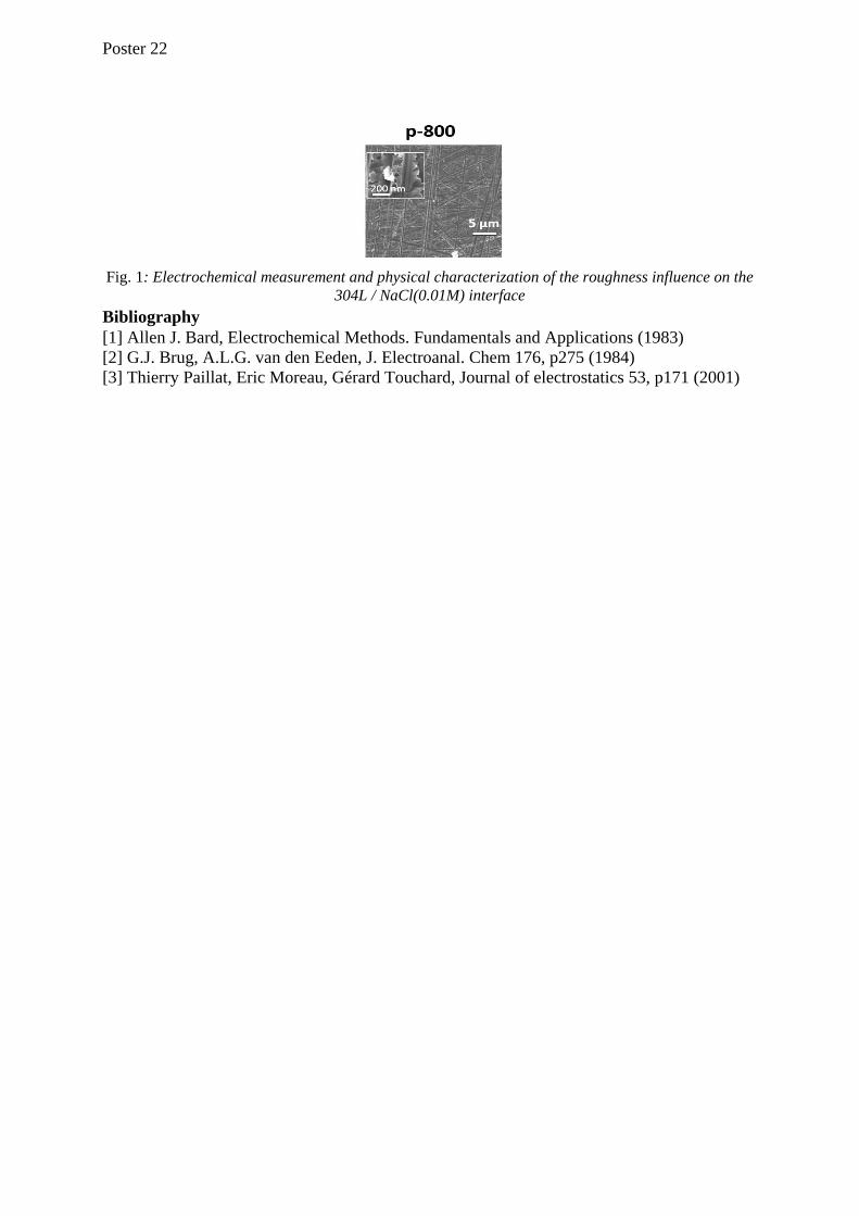
Poster 22
Fig. 1: Electrochemical measurement and physical characterization of the roughness influence on the
304L / NaCl(0.01M) interface
Bibliography
[1] Allen J. Bard, Electrochemical Methods. Fundamentals and Applications (1983)
[2] G.J. Brug, A.L.G. van den Eeden, J. Electroanal. Chem 176, p275 (1984)
[3] Thierry Paillat, Eric Moreau, Gérard Touchard, Journal of electrostatics 53, p171 (2001)
Poster 23
Interaction of native and dry-heated ovotransferrin
with E.coli lipopolysaccharide monolayer
Youcef Menacer *a, Gilles Paboeuf a, Catherine Guérin b, Françoise Nau b, Véronique Vié a
a) Physics Institute of Rennes, Rennes 1 University, UMR6251, Rennes, France b) INRA, Science and Technology of Milk and Egg, UMR1253, Rennes, France
The constant development of bacterial multiresistance to antibiotics and nosocomial
infections is a permanent concern towards the public health authorities. In addition, the
development of new antibiotics is constantly faced with bacterial adaptive strategies to establish a
resistance process. Otherwise, some peptides/proteins possess an antibacterial activity leading to
limit resistance development. They thus appear to be an alternative to face the bacterial resistance
process and provide an opportunity for the current research.
Ovotransferrin is an egg white protein with an antimicrobial broad-spectrum activity.
Especially, Escherichia coli is sensitive to the ovotransferrin which disrupts the bacterial outer
membrane [1, 2]. The dry-heating ovotransferrin treatment modifies its properties with
consequences on its antibacterial activity. In order to understand the mechanisms underlying the
antibacterial activity of native ovotransferrin, and the effect of dry-heating on its activity, it is
necessary to investigate the interactions of the protein with the E. coli outer membrane.
In this study, these interactions were characterized by using an in vitro membrane model
which is a lipopolysaccharide monolayer at the air-water interface. Protein-membrane interactions
were examined by ellipsometry, tensiometry and imaging techniques (Brewster Angle Microscopy
and Atomic Force Microscopy).
The results showed that ovotransferrin had an affinity to lipopolysaccharides and inserted
into the monolayer, the delta signal and the surface pressure increased. Therefore, the AFM images
showed an increase of the monolayer roughness and changes on the lipopolysaccharide
organization. Dry-heating enhanced the ovotransferrin affinity to lipopolysaccharides and
increased its membrane activity. Moreover, this affinity was impacted by the molecular state of
lipopolysaccharides which can be modulated changing the surface pressure.
The insertion into E. coli outer membrane and the disorganization of lipopolysaccharides
due to ovotransferrin could explain its antibacterial activity. Otherwise, dry-heating appeared as a
simple way to enhance the ovotransferrin antibacterial activity.
[1] P. Valenti, G. Antonini, C. Von Hunolstein, P. Visca, N. Orsi, and E. Antonini, "Studies of the antimicrobial
activity of ovotransferrin," International journal of tissue reactions, vol. 5, pp. 97-105, 1982.
[2] O. Aguilera, L. M. Quiros, and J. F. Fierro, "Transferrins selectively cause ion efflux through bacterial and
artificial membranes," FEBS Letters, vol. 548, pp. 5-10, 2003.
Poster 24
Effets de ségrégation de surface et d’alliage dans les
nanoparticules Pt-Ag
J. Pirart1, C. Andreazza-Vignolle1, P. Andreazza1, C. Mottet2, A. Lemoine1,3, Y.
Garreau3, A. Coati3 1. Interfaces, Confinement, Matériaux et Nanostructures, Univ. Orléans, 1bis rue de la Férollerie, 45071
Orléans Cedex 2, France. 2. Centre Interdisciplinaire de Nanoscience de Marseille, Campus de Luminy, Marseille, France.
3. Synchrotron Soleil, L'Orme de Merisiers, Saint Aubin, 91192 Gif-sur-Yvette, France.
E-mail: [email protected]
L’intérêt porté aux nano-objets, notamment aux nanoalliages, est dû aux nombreuses
propriétés physico-chimiques qui en découlent, elles-mêmes dues aux effets de réduction de
taille des objets qui seraient trop simpliste de résumer au seul effet de surface. En effet, un
autre effet apparait, c’est celui de la quantité finie d’atomes qui en font des objets très
différents du massif et de la surface infinie. Ces caractéristiques modifient en premier lieu la
structure atomique et chimique des nanoalliages : l’arrangement des atomes, mais également
les déformations internes induites par cette échelle nanométrique.
L’étude à l’échelle macroscopique de l’alliage Pt-Ag montre un diagramme de phase
[1] intéressant mais complexe notamment à basse température : présence d’un alliage ordonné
uniquement à l’équiconcentration AgPt, une immiscibilité presque totale pour les fortes
concentrations en Pt mais partielle à forte concentration en Ag. La réduction de taille peut
conduire à une modification de la stabilité des alliages ordonnés ou induire une ségrégation
entre les deux éléments pour former une particule de type cœur-coquille, janus-like…
Trois forces principales permettent de prédire la tendance du système (alliage /
ségrégation) : le désaccord de maille, la différence d’énergie de surface entre les deux
éléments ainsi que l’énergie de mélange du système. Dans le cas de Pt-Ag, des études
numériques basées sur la méthode Monte Carlo [2], prenant en compte ces forces motrices,
ont tendances à prédire une ségrégation de type cœur(Pt)-coquille(Ag), en compétition avec
un effet de mélange selon la composition. Notre objectif est de déterminer expérimentalement,
en fonction de la composition de la nanoparticule, quelle sera la conséquence des effets de
surface : l’effet de ségrégation de surface de l’argent va-t-il être prédominant sur les effets
d’alliage qui ont été montrés sur le massif ?
Les particules Pt-Ag sont préparées en co-dépôt sous ultravide par évaporation des
deux éléments. La structure et la configuration chimique du système ont pu être observées
d’une part ex situ par microscopie électronique à transmission à très haute résolution
notamment en mode HAADF, et d’autre part in situ et en temps réel sur la ligne SIXS du
synchrotron SOLEIL par diffusion des rayons X en incidence rasante montrant une phase
alliée avec une tendance à l’ordre après recuit thermique. Ainsi une phase d’alliage L11
(alternance de plans Ag puis Pt dans la direction [111]) avec une déformation rhomboédrique
très marquée a été observée, mais aussi une ségrégation cœur-coquille, comportement
dépendant de la composition.
Bibliographie [1] M H. F. Sluiter, C. Colinet, A. Pasturel, Ab initio calculation of the phase stability in Au-Pd and
Ag-Pt alloys, Phys. Rev. B, 2006.
[2] K. Yun et al, Monte Carlo simulations of the structure of Pt-based bimetallic nanoparticles, Acta
materiala 60,12, 4908-4916, 2012.
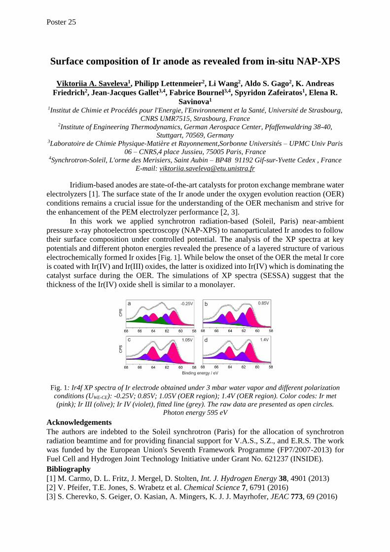
Poster 25
Surface composition of Ir anode as revealed from in-situ NAP-XPS
Viktoriia A. Saveleva1, Philipp Lettenmeier2, Li Wang2, Aldo S. Gago2, K. Andreas
Friedrich2, Jean-Jacques Gallet3,4, Fabrice Bournel3,4, Spyridon Zafeiratos1, Elena R.
Savinova1 1Institut de Chimie et Procédés pour l'Energie, l'Environnement et la Santé, Université de Strasbourg,
CNRS UMR7515, Strasbourg, France 2Institute of Engineering Thermodynamics, German Aerospace Center, Pfaffenwaldring 38-40,
Stuttgart, 70569, Germany 3Laboratoire de Chimie Physique-Matière et Rayonnement,Sorbonne Universités – UPMC Univ Paris
06 – CNRS,4 place Jussieu, 75005 Paris, France 4Synchrotron-Soleil, L'orme des Merisiers, Saint Aubin – BP48 91192 Gif-sur-Yvette Cedex , France
E-mail: [email protected]
Iridium-based anodes are state-of-the-art catalysts for proton exchange membrane water
electrolyzers [1]. The surface state of the Ir anode under the oxygen evolution reaction (OER)
conditions remains a crucial issue for the understanding of the OER mechanism and strive for
the enhancement of the PEM electrolyzer performance [2, 3].
In this work we applied synchrotron radiation-based (Soleil, Paris) near-ambient
pressure x-ray photoelectron spectroscopy (NAP-XPS) to nanoparticulated Ir anodes to follow
their surface composition under controlled potential. The analysis of the XP spectra at key
potentials and different photon energies revealed the presence of a layered structure of various
electrochemically formed Ir oxides [Fig. 1]. While below the onset of the OER the metal Ir core
is coated with Ir(IV) and Ir(III) oxides, the latter is oxidized into Ir(IV) which is dominating the
catalyst surface during the OER. The simulations of XP spectra (SESSA) suggest that the
thickness of the Ir(IV) oxide shell is similar to a monolayer.
Fig. 1: Ir4f XP spectra of Ir electrode obtained under 3 mbar water vapor and different polarization
conditions (UWE-CE): -0.25V; 0.85V; 1.05V (OER region); 1.4V (OER region). Color codes: Ir met
(pink); Ir III (olive); Ir IV (violet), fitted line (grey). The raw data are presented as open circles.
Photon energy 595 eV
Acknowledgements
The authors are indebted to the Soleil synchrotron (Paris) for the allocation of synchrotron
radiation beamtime and for providing financial support for V.A.S., S.Z., and E.R.S. The work
was funded by the European Union's Seventh Framework Programme (FP7/2007-2013) for
Fuel Cell and Hydrogen Joint Technology Initiative under Grant No. 621237 (INSIDE).
Bibliography
[1] M. Carmo, D. L. Fritz, J. Mergel, D. Stolten, Int. J. Hydrogen Energy 38, 4901 (2013)
[2] V. Pfeifer, T.E. Jones, S. Wrabetz et al. Chemical Science 7, 6791 (2016)
[3] S. Cherevko, S. Geiger, O. Kasian, A. Mingers, K. J. J. Mayrhofer, JEAC 773, 69 (2016)
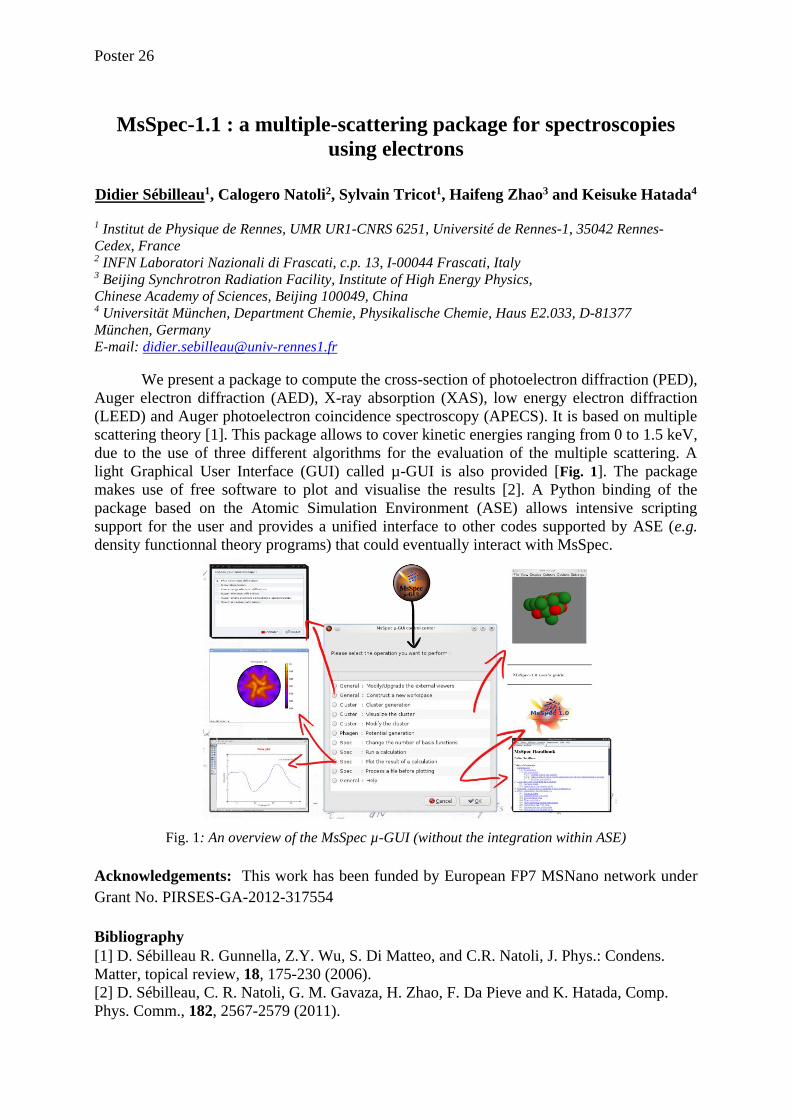
Poster 26
MsSpec-1.1 : a multiple-scattering package for spectroscopies
using electrons
Didier Sébilleau1, Calogero Natoli2, Sylvain Tricot1, Haifeng Zhao3 and Keisuke Hatada4
1 Institut de Physique de Rennes, UMR UR1-CNRS 6251, Université de Rennes-1, 35042 Rennes-
Cedex, France
2 INFN Laboratori Nazionali di Frascati, c.p. 13, I-00044 Frascati, Italy
3 Beijing Synchrotron Radiation Facility, Institute of High Energy Physics,
Chinese Academy of Sciences, Beijing 100049, China
4 Universität München, Department Chemie, Physikalische Chemie, Haus E2.033, D-81377
München, Germany
E-mail: [email protected]
We present a package to compute the cross-section of photoelectron diffraction (PED),
Auger electron diffraction (AED), X-ray absorption (XAS), low energy electron diffraction
(LEED) and Auger photoelectron coincidence spectroscopy (APECS). It is based on multiple
scattering theory [1]. This package allows to cover kinetic energies ranging from 0 to 1.5 keV,
due to the use of three different algorithms for the evaluation of the multiple scattering. A
light Graphical User Interface (GUI) called µ-GUI is also provided [Fig. 1]. The package
makes use of free software to plot and visualise the results [2]. A Python binding of the
package based on the Atomic Simulation Environment (ASE) allows intensive scripting
support for the user and provides a unified interface to other codes supported by ASE (e.g.
density functionnal theory programs) that could eventually interact with MsSpec.
Fig. 1: An overview of the MsSpec µ-GUI (without the integration within ASE)
Acknowledgements: This work has been funded by European FP7 MSNano network under
Grant No. PIRSES-GA-2012-317554
Bibliography
[1] D. Sébilleau R. Gunnella, Z.Y. Wu, S. Di Matteo, and C.R. Natoli, J. Phys.: Condens.
Matter, topical review, 18, 175-230 (2006).
[2] D. Sébilleau, C. R. Natoli, G. M. Gavaza, H. Zhao, F. Da Pieve and K. Hatada, Comp.
Phys. Comm., 182, 2567-2579 (2011).
Poster 27
Germanène sur Al(111) : étude de la structure électronique
R. Stephan1, M.-C. Hanf1, M. Derivaz1, D. Dentel1, A. Mehdaoui1, M. C. Asensio2, J.
Avila2, Ph. Sonnet1 et C. Pirri1
1Institut de Science des Matériaux de Mulhouse (IS2M), CNRS UMR 7361, Université de Haute
Alsace, 3b rue Alfred Werner 68093 Mulhouse cedex, France 2 Synchrotron SOLEIL, Saint Aubin, BP 48 91192 Gif-sur-Yvette, France
E-mail: [email protected]
La découverte du graphène a fortement stimulé la recherche sur les matériaux 2D.
Récemment, le silicene, cousin du graphène pour le silicium, a été synthétisé sur un substrat
métallique d’argent (111). Ces dernières années, le silicène a également été observé sur des
surfaces de dibore de zirconium (0001) ou d’iridium (111). Le germanène, un autre cousin du
graphène mais à base de germanium, a été prédit en 2009 comme étant une phase stable du
germanium et observé en multiphase sur un substrat d’or (111) en 2014 [1]. La synthèse et
l’étude d’une couche de germanène sur d’autres substrats permettrait de comprendre comment
se forme ce type de couche 2D.
Dans ce travail, nous avons élaboré et caractérisé une couche de germanène déposée
sur un substrat d’aluminium orienté dans la direction (111) [2]. La structure électronique de
germanène a été étudiée par photoémission haute résolution et par des calculs DFT [3]. Les
niveaux de cœur Al 2p et Ge 3d ont été mesurés sur le système germanène/Al(111) en par
rayonnement synchrotron (SOLEIL, ligne ANTARES). Le niveau Ge 3d est déplacé vers les
faibles énergies de liaison par rapport au germanium volumique et montre trois composantes
qui reflètent la multiplicité des sites atomiques dans le germanène. Les calculs révèlent la
présence d’une densité de charge à l’interface germanène/Al(111) ainsi qu’un transfert de
charge des atomes d’aluminium de surface vers le germanène. L’existence de trois sites
atomiques non équivalents dans la couche de germanène est associée à trois charges de Bader
différentes, pouvant ainsi expliquer les mesures de photoémission présentant trois
composantes.
En conclusion, les résultats obtenus montrent qu’il y a un transfert de charge entre
l’aluminium et le germanium, conduisant à une interaction électrostatique entre le substrat
d’aluminium et le germanène. De plus, la présence d’une densité de charge à l’interface
indique l’existence d’une interaction chimique faible entre la surface d’aluminium et la
couche de germanène. Ainsi, l’interaction du germanène avec le substrat Al(111) présente des
similarités avec celle du silicène/Ag(111) [4]. La structure électronique de ces deux systèmes
semble être une caractéristique des éléments du groupe IV en couche 2D déposés sur des
métaux simples ou nobles.
Bibliography [1] M. Davila, L.Xian, S. Cahangirov, A. Rubio, G. Le Lay, New J. Phys. 16, 095002 (2014).
[2] M. Derivaz, D. Dentel, R. Stephan, M.-C. Hanf, A. Mehdaoui, Ph. Sonnet, C. Pirri, Nano Lett. 15, 2510
(2015).
[3] R. Stephan, M.C. Hanf, M. Derivaz, D. Dentel, M. C. Asensio, J. Avila, A. Mehdaoui, Ph. Sonnet, C. Pirri, J.
Phys. Chem. C 120, 1580 (2016).
[4] R. Stephan, M-C. Hanf, Ph. Sonnet, J. Phys.: Condens. Matter 27, 015002 (2015).
Poster 28
Moduler les interactions germanène-substrat au moyen de
l’hydrogénation A. Marjaoui1,2, R. Stephan1, M.-C. Hanf1, M. Diani2 et Ph. Sonnet1
1Institut de Science des Matériaux de Mulhouse (IS2M), CNRS UMR 7361, Université de Haute
Alsace, 3b rue Alfred Werner 68093 Mulhouse cedex, France 2 Laboratoire des Matériaux et Valorisation des Ressources, Université Abdelmalek
Essaâdi, FST, ancienne route de l’aéroport, Km10, Ziaten, BP416, 90050, Tanger,
Morocco
E-mail: [email protected]
Le germanène, un cousin du graphène mais à base de germanium, a été prédit en 2009
comme étant une phase stable du germanium, et observé en multiphase sur un substrat d’or
(111) en 2014 [1]. Récemment, une couche de germanène déposée sur un substrat
d’aluminium a pu être obtenue et caractérisée dans notre laboratoire [2]. Nos études DFT ont
montré qu’il y avait un transfert de charge entre l’aluminium et le germanium conduisant à
une interaction électrostatique entre le substrat d’aluminium et le germanène. De plus, la
présence d’une densité de charge à l’interface indiquait l’existence d’une interaction chimique
faible entre la surface d’aluminium et la couche de germanène [3]. Cependant pour des
applications futures, il serait intéressant d’exfolier une couche de germanène de son substrat.
Pour cette raison, nous avons étudié l’hydrogénation du système germanène/Al au moyen de
calculs DFT [4].
Nous montrons que les atomes de germanium portant un atome d’hydrogène sont plus
éloignés de la surface d’aluminium que les autres atomes de germanium. Ainsi, la distance
Ge-Al augmente lorsque que le recouvrement en hydrogène augmente, tandis que l’énergie
d’interaction diminue. De plus, le transfert de charge des atomes d’aluminium vers la couche
de germanium diminue également, conduisant à réduire les interactions électrostatiques entre
le germanène et le substrat d’aluminium. Les calculs de densité de charge et de différence de
densité de charge indiquent que la densité électronique localisée à l’interface est fortement
réduite sous hydrogénation. Tous ces résultats montrent clairement que les interactions entre
le germanium et le substrat d’aluminium diminuent en présence d’hydrogène. Cependant
l’hydrogénation représente seulement la première étape pour une éventuelle exfoliation d’une
couche de germanène. Une autre étape est nécessaire pour finaliser la séparation entre la
couche 2D et le substrat. Ainsi, l’augmentation de la distance entre le germanène et les
atomes d’Al pourrait faciliter l’intercalation de différentes espèces atomiques permettant ainsi
une séparation définitive.
Bibliography
[1] M. Davila, L.Xian, S. Cahangirov, A. Rubio, G. Le Lay, New J. Phys. 16, 095002 (2014).
[2] M. Derivaz, D. Dentel, R. Stephan, M.-C. Hanf, A. Mehdaoui, Ph. Sonnet, C. Pirri, Nano Lett. 15, 2510
(2015).
[3] R. Stephan, M.C. Hanf, M. Derivaz, D. Dentel, M. C. Asensio, J. Avila, A. Mehdaoui, Ph. Sonnet, C. Pirri, J.
Phys. Chem. C 120, 1580 (2016).
[4] A. Marjaoui, R. Stephan, M-C. Hanf, M.Diani, Ph. Sonnet, Phys.Chem.Chem.Phys. 18, 15667 (2016).
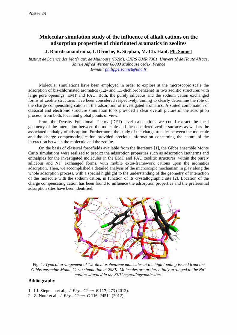
Poster 29
Molecular simulation study of the influence of alkali cations on the
adsorption properties of chlorinated aromatics in zeolites
J. Ranrdrianandraina, I. Déroche, R. Stephan, M.-Ch. Hanf, Ph. Sonnet
Institut de Science des Matériaux de Mulhouse (IS2M), CNRS UMR 7361, Université de Haute Alsace,
3b rue Alfred Werner 68093 Mulhouse cedex, France E-mail: [email protected]
Molecular simulations have been employed in order to explore at the microscopic scale the
adsorption of bis-chlorinated aromatics (1,2- and 1,3-dichlorobenzene) in two zeolitic structures with
large pore openings: EMT and FAU. Both, the purely siliceous and the sodium cation exchanged
forms of zeolite structures have been considered respectively, aiming to clearly determine the role of
the charge compensating cation in the adsorption of investigated aromatics. A suited combination of
classical and electronic structure simulation tools provided a clear overall picture of the adsorption
process, from both, local and global points of view.
From the Density Functional Theory (DFT) level calculations we could extract the local
geometry of the interaction between the molecule and the considered zeolite surfaces as well as the
associated enthalpy of adsorption. Furthermore, the study of the charge transfer between the molecule
and the charge compensating cation provided precious information concerning the nature of the
interaction between the molecule and the zeolite.
On the basis of classical forcefields available from the literature [1], the Gibbs ensemble Monte
Carlo simulations were realized to predict the adsorption properties such as adsorption isotherms and
enthalpies for the investigated molecules in the EMT and FAU zeolitic structures, within the purely
siliceous and Na+ exchanged forms, with mobile extra-framework cations upon the aromatics
adsorption. Then, we accomplished a detailed analysis of the microscopic mechanism in play along the
whole adsorption process, with a special highlight to the understanding of the geometry of interaction
of the molecule with the sodium cation, in function of its crystallographic site [2]. Location of the
charge compensating cation has been found to influence the adsorption properties and the preferential
adsorption sites have been identified.
Fig. 1: Typical arrangement of 1.2-dichlorobenzene molecules at the high loading issued from the
Gibbs ensemble Monte Carlo simulation at 298K. Molecules are preferentially arranged to the Na+
cations situated in the SIII’ crystallographic sites.
Bibliography
1. I.J. Siepman et al., J. Phys. Chem. B 117, 273 (2012).
2. Z. Nour et al., J. Phys. Chem. C.116, 24512 (2012)
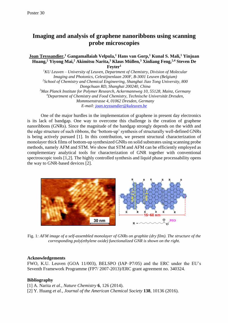
Poster 30
Imaging and analysis of graphene nanoribbons using scanning
probe microscopies
Joan Teyssandier,1 Gangamallaiah Velpula,1 Hans van Gorp,1 Kunal S. Mali,1 Yinjuan
Huang,2 Yiyong Mai,2 Akimitsu Narita,3 Klaus Müllen,3 Xinliang Feng,2,4 Steven De
Feyter1 1KU Leuven – University of Leuven, Department of Chemistry, Division of Molecular
Imaging and Photonics, Celestijnenlaan 200F, B-3001 Leuven (Belgium) 2School of Chemistry and Chemical Engineering, Shanghai Jiao Tong University, 800
Dongchuan RD, Shanghai 200240, China 3Max Planck Institute for Polymer Research, Ackermannweg 10, 55128, Mainz, Germany
4Department of Chemistry and Food Chemistry, Technische Universität Dresden,
Mommsenstrasse 4, 01062 Dresden, Germany
E-mail: [email protected]
One of the major hurdles in the implementation of graphene in present day electronics
is its lack of bandgap. One way to overcome this challenge is the creation of graphene
nanoribbons (GNRs). Since the magnitude of the bandgap strongly depends on the width and
the edge structure of such ribbons, the ‘bottom-up’ synthesis of structurally well-defined GNRs
is being actively pursued [1]. In this contribution, we present structural characterization of
monolayer thick films of bottom-up synthesized GNRs on solid substrates using scanning probe
methods, namely AFM and STM. We show that STM and AFM can be efficiently employed as
complementary analytical tools for characterization of GNR together with conventional
spectroscopic tools [1,2]. The highly controlled synthesis and liquid phase processability opens
the way to GNR-based devices [2].
Fig. 1: AFM image of a self-assembled monolayer of GNRs on graphite (dry film). The structure of the
corresponding poly(ethylene oxide) functionalized GNR is shown on the right.
Acknowledgements
FWO, K.U. Leuven (GOA 11/003), BELSPO (IAP–P7/05) and the ERC under the EU’s
Seventh Framework Programme (FP7/ 2007-2013)/ERC grant agreement no. 340324.
Bibliography
[1] A. Narita et al., Nature Chemistry 6, 126 (2014).
[2] Y. Huang et al., Journal of the American Chemical Society 138, 10136 (2016).
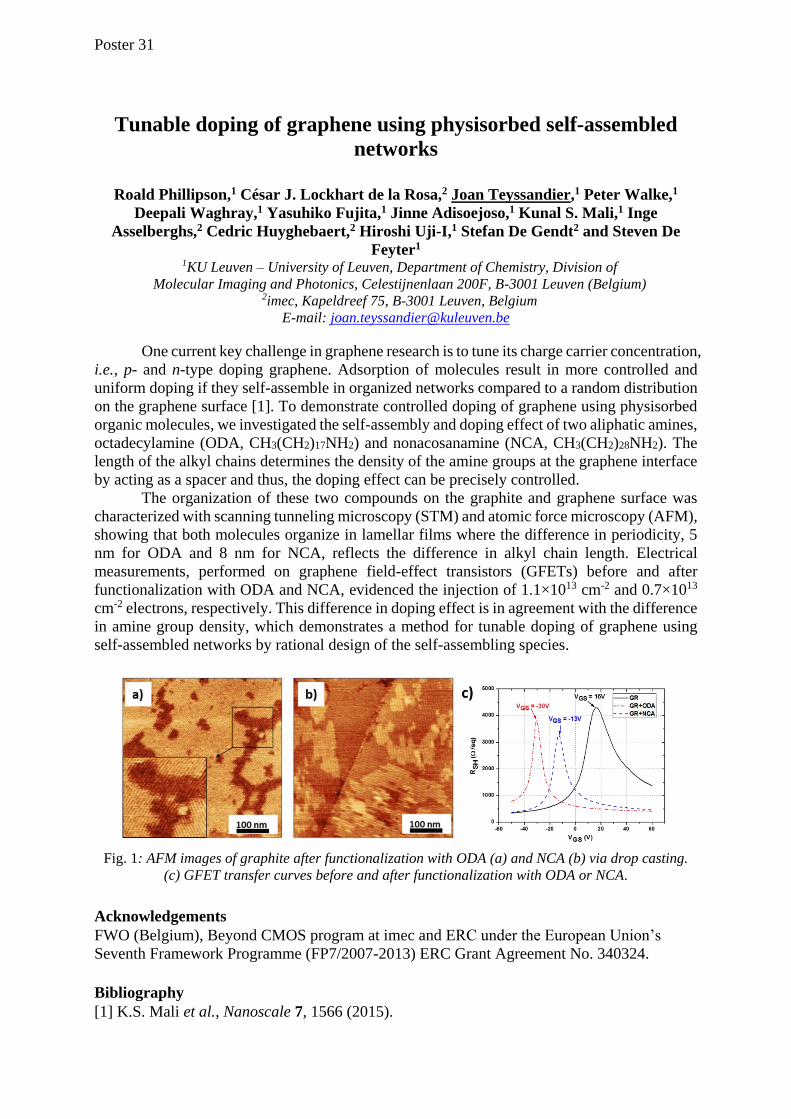
Poster 31
Tunable doping of graphene using physisorbed self-assembled
networks
Roald Phillipson,1 César J. Lockhart de la Rosa,2 Joan Teyssandier,1 Peter Walke,1
Deepali Waghray,1 Yasuhiko Fujita,1 Jinne Adisoejoso,1 Kunal S. Mali,1 Inge
Asselberghs,2 Cedric Huyghebaert,2 Hiroshi Uji-I,1 Stefan De Gendt2 and Steven De
Feyter1 1KU Leuven – University of Leuven, Department of Chemistry, Division of
Molecular Imaging and Photonics, Celestijnenlaan 200F, B-3001 Leuven (Belgium) 2imec, Kapeldreef 75, B-3001 Leuven, Belgium
E-mail: [email protected]
One current key challenge in graphene research is to tune its charge carrier concentration,
i.e., p- and n-type doping graphene. Adsorption of molecules result in more controlled and
uniform doping if they self-assemble in organized networks compared to a random distribution
on the graphene surface [1]. To demonstrate controlled doping of graphene using physisorbed
organic molecules, we investigated the self-assembly and doping effect of two aliphatic amines,
octadecylamine (ODA, CH3(CH2)17NH2) and nonacosanamine (NCA, CH3(CH2)28NH2). The
length of the alkyl chains determines the density of the amine groups at the graphene interface
by acting as a spacer and thus, the doping effect can be precisely controlled.
The organization of these two compounds on the graphite and graphene surface was
characterized with scanning tunneling microscopy (STM) and atomic force microscopy (AFM),
showing that both molecules organize in lamellar films where the difference in periodicity, 5
nm for ODA and 8 nm for NCA, reflects the difference in alkyl chain length. Electrical
measurements, performed on graphene field-effect transistors (GFETs) before and after
functionalization with ODA and NCA, evidenced the injection of 1.1×1013 cm-2 and 0.7×10¹³
cm-2 electrons, respectively. This difference in doping effect is in agreement with the difference
in amine group density, which demonstrates a method for tunable doping of graphene using
self-assembled networks by rational design of the self-assembling species.
Fig. 1: AFM images of graphite after functionalization with ODA (a) and NCA (b) via drop casting.
(c) GFET transfer curves before and after functionalization with ODA or NCA.
Acknowledgements
FWO (Belgium), Beyond CMOS program at imec and ERC under the European Union’s
Seventh Framework Programme (FP7/2007-2013) ERC Grant Agreement No. 340324.
Bibliography
[1] K.S. Mali et al., Nanoscale 7, 1566 (2015).
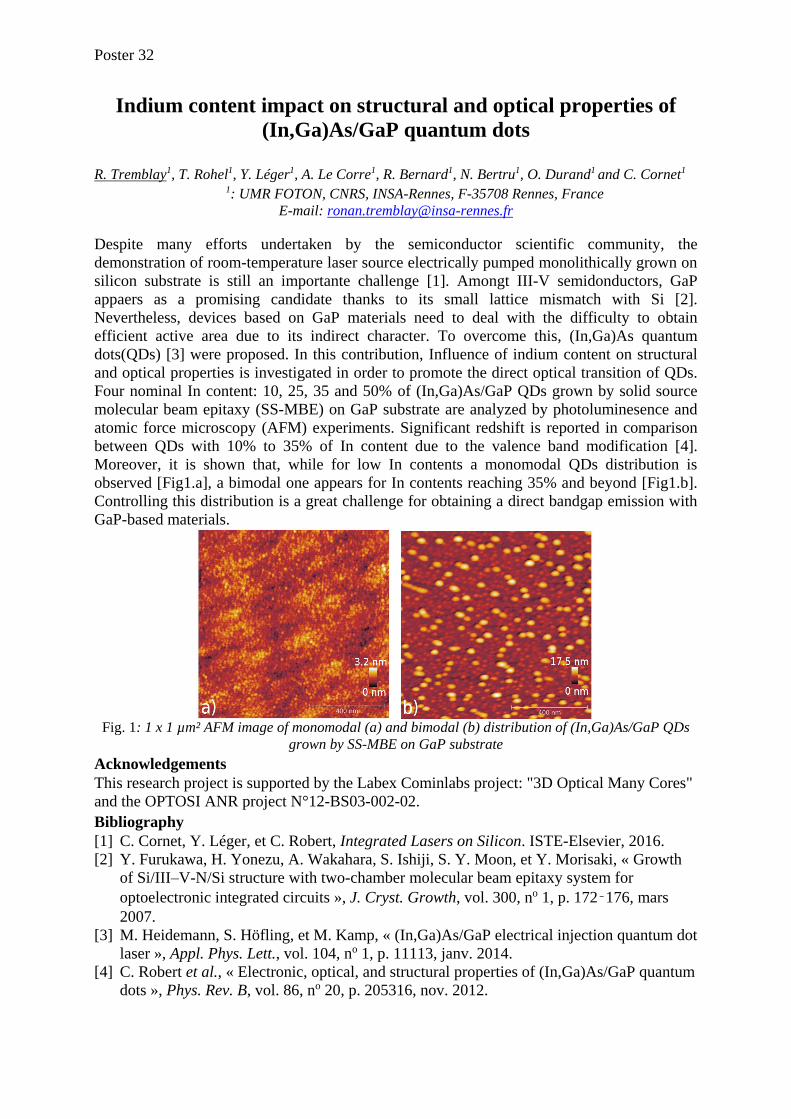
Poster 32
Indium content impact on structural and optical properties of
(In,Ga)As/GaP quantum dots
R. Tremblay1, T. Rohel1, Y. Léger1, A. Le Corre1, R. Bernard1, N. Bertru1, O. Durand1 and C. Cornet1 1: UMR FOTON, CNRS, INSA-Rennes, F-35708 Rennes, France
E-mail: [email protected]
Despite many efforts undertaken by the semiconductor scientific community, the
demonstration of room-temperature laser source electrically pumped monolithically grown on
silicon substrate is still an importante challenge [1]. Amongt III-V semidonductors, GaP
appaers as a promising candidate thanks to its small lattice mismatch with Si [2].
Nevertheless, devices based on GaP materials need to deal with the difficulty to obtain
efficient active area due to its indirect character. To overcome this, (In,Ga)As quantum
dots(QDs) [3] were proposed. In this contribution, Influence of indium content on structural
and optical properties is investigated in order to promote the direct optical transition of QDs.
Four nominal In content: 10, 25, 35 and 50% of (In,Ga)As/GaP QDs grown by solid source
molecular beam epitaxy (SS-MBE) on GaP substrate are analyzed by photoluminesence and
atomic force microscopy (AFM) experiments. Significant redshift is reported in comparison
between QDs with 10% to 35% of In content due to the valence band modification [4].
Moreover, it is shown that, while for low In contents a monomodal QDs distribution is
observed [Fig1.a], a bimodal one appears for In contents reaching 35% and beyond [Fig1.b].
Controlling this distribution is a great challenge for obtaining a direct bandgap emission with
GaP-based materials.
Fig. 1: 1 x 1 µm² AFM image of monomodal (a) and bimodal (b) distribution of (In,Ga)As/GaP QDs
grown by SS-MBE on GaP substrate
Acknowledgements
This research project is supported by the Labex Cominlabs project: "3D Optical Many Cores"
and the OPTOSI ANR project N°12-BS03-002-02.
Bibliography
[1] C. Cornet, Y. Léger, et C. Robert, Integrated Lasers on Silicon. ISTE-Elsevier, 2016.
[2] Y. Furukawa, H. Yonezu, A. Wakahara, S. Ishiji, S. Y. Moon, et Y. Morisaki, « Growth
of Si/III–V-N/Si structure with two-chamber molecular beam epitaxy system for
optoelectronic integrated circuits », J. Cryst. Growth, vol. 300, no 1, p. 172‑176, mars
2007.
[3] M. Heidemann, S. Höfling, et M. Kamp, « (In,Ga)As/GaP electrical injection quantum dot
laser », Appl. Phys. Lett., vol. 104, no 1, p. 11113, janv. 2014.
[4] C. Robert et al., « Electronic, optical, and structural properties of (In,Ga)As/GaP quantum
dots », Phys. Rev. B, vol. 86, no 20, p. 205316, nov. 2012.
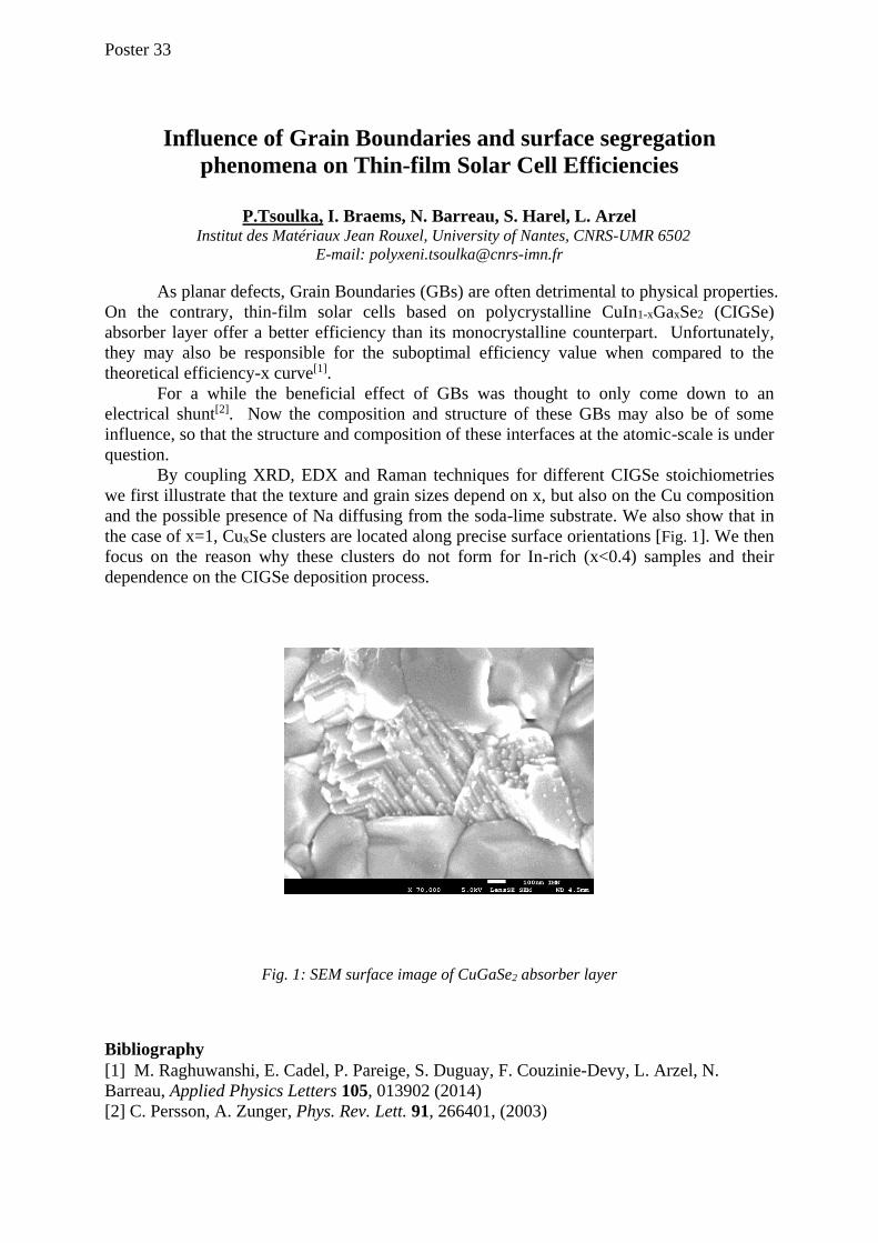
Poster 33
Influence of Grain Boundaries and surface segregation
phenomena on Thin-film Solar Cell Efficiencies
P.Tsoulka, I. Braems, N. Barreau, S. Harel, L. Arzel
Institut des Matériaux Jean Rouxel, University of Nantes, CNRS-UMR 6502
E-mail: [email protected]
As planar defects, Grain Boundaries (GBs) are often detrimental to physical properties.
On the contrary, thin-film solar cells based on polycrystalline CuIn1-xGaxSe2 (CIGSe)
absorber layer offer a better efficiency than its monocrystalline counterpart. Unfortunately,
they may also be responsible for the suboptimal efficiency value when compared to the
theoretical efficiency-x curve[1].
For a while the beneficial effect of GBs was thought to only come down to an
electrical shunt[2]. Now the composition and structure of these GBs may also be of some
influence, so that the structure and composition of these interfaces at the atomic-scale is under
question.
By coupling XRD, EDX and Raman techniques for different CIGSe stoichiometries
we first illustrate that the texture and grain sizes depend on x, but also on the Cu composition
and the possible presence of Na diffusing from the soda-lime substrate. We also show that in
the case of x=1, CuxSe clusters are located along precise surface orientations [Fig. 1]. We then
focus on the reason why these clusters do not form for In-rich (x<0.4) samples and their
dependence on the CIGSe deposition process.
Fig. 1: SEM surface image of CuGaSe2 absorber layer
Bibliography
[1] M. Raghuwanshi, E. Cadel, P. Pareige, S. Duguay, F. Couzinie-Devy, L. Arzel, N.
Barreau, Applied Physics Letters 105, 013902 (2014)
[2] C. Persson, A. Zunger, Phys. Rev. Lett. 91, 266401, (2003)
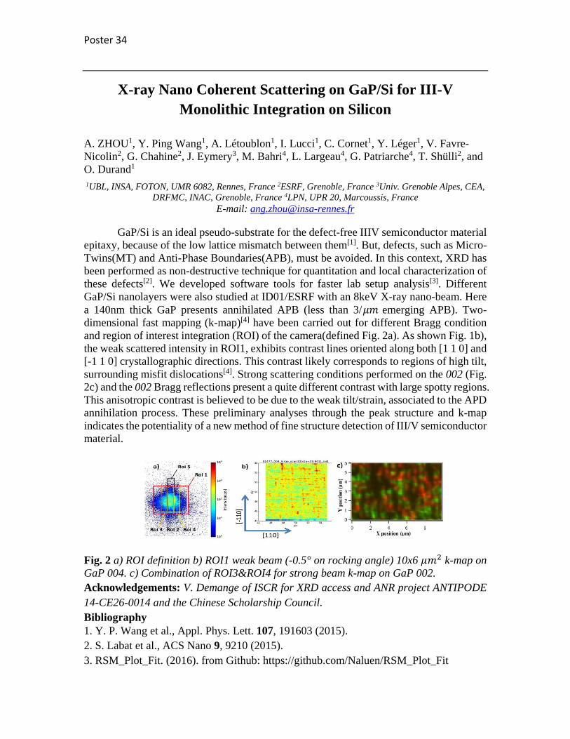
Poster 34
X-ray Nano Coherent Scattering on GaP/Si for III-V
Monolithic Integration on Silicon
A. ZHOU1, Y. Ping Wang1, A. Létoublon1, I. Lucci1, C. Cornet1, Y. Léger1, V. Favre-
Nicolin2, G. Chahine2, J. Eymery3, M. Bahri4, L. Largeau4, G. Patriarche4, T. Shülli2, and
O. Durand1
1UBL, INSA, FOTON, UMR 6082, Rennes, France 2ESRF, Grenoble, France 3Univ. Grenoble Alpes, CEA,
DRFMC, INAC, Grenoble, France 4LPN, UPR 20, Marcoussis, France
E-mail: [email protected]
GaP/Si is an ideal pseudo-substrate for the defect-free IIIV semiconductor material
epitaxy, because of the low lattice mismatch between them[1]. But, defects, such as Micro-
Twins(MT) and Anti-Phase Boundaries(APB), must be avoided. In this context, XRD has
been performed as non-destructive technique for quantitation and local characterization of
these defects[2]. We developed software tools for faster lab setup analysis[3]. Different
GaP/Si nanolayers were also studied at ID01/ESRF with an 8keV X-ray nano-beam. Here
a 140nm thick GaP presents annihilated APB (less than 3/𝜇𝑚 emerging APB). Two-
dimensional fast mapping (k-map)[4] have been carried out for different Bragg condition
and region of interest integration (ROI) of the camera(defined Fig. 2a). As shown Fig. 1b),
the weak scattered intensity in ROI1, exhibits contrast lines oriented along both [1 1 0] and
[-1 1 0] crystallographic directions. This contrast likely corresponds to regions of high tilt,
surrounding misfit dislocations[4]. Strong scattering conditions performed on the 002 (Fig.
2c) and the 002 Bragg reflections present a quite different contrast with large spotty regions.
This anisotropic contrast is believed to be due to the weak tilt/strain, associated to the APD
annihilation process. These preliminary analyses through the peak structure and k-map
indicates the potentiality of a new method of fine structure detection of III/V semiconductor
material.
Fig. 2 a) ROI definition b) ROI1 weak beam (-0.5° on rocking angle) 10x6 𝜇𝑚2 k-map on
GaP 004. c) Combination of ROI3&ROI4 for strong beam k-map on GaP 002.
Acknowledgements: V. Demange of ISCR for XRD access and ANR project ANTIPODE
14-CE26-0014 and the Chinese Scholarship Council.
Bibliography
1. Y. P. Wang et al., Appl. Phys. Lett. 107, 191603 (2015).
2. S. Labat et al., ACS Nano 9, 9210 (2015).
3. RSM_Plot_Fit. (2016). from Github: https://github.com/Naluen/RSM_Plot_Fit

Poster 34
4. M. H. Zoellner et al., ACS Appl. Mater. Interfaces 7, 9031 (2015).
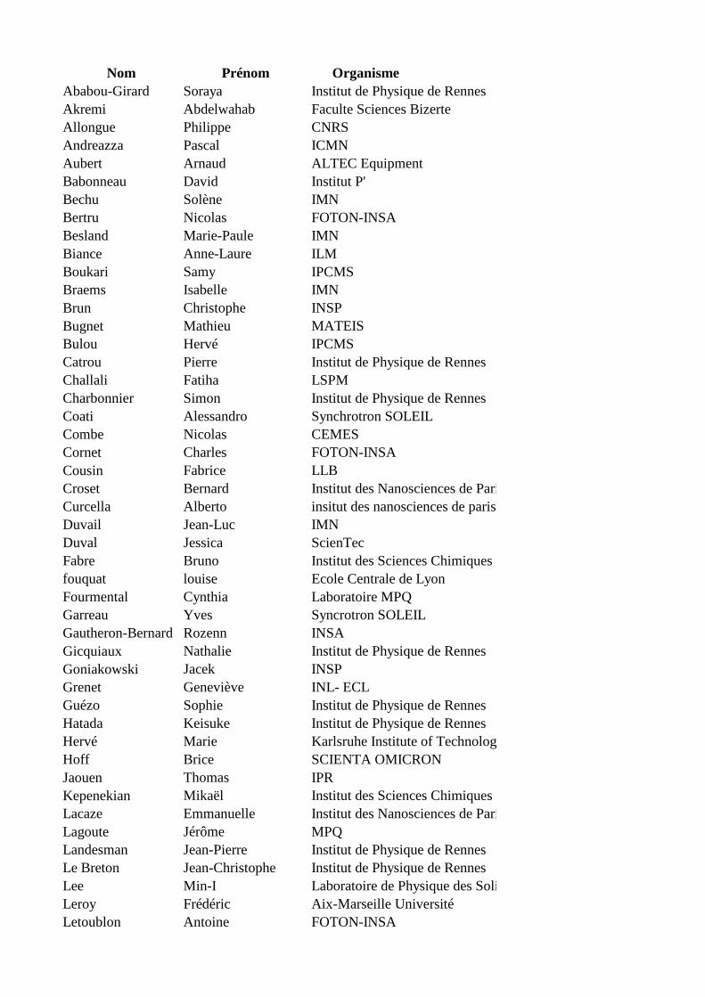
Nom Prénom Organisme
Ababou-Girard Soraya Institut de Physique de Rennes
Akremi Abdelwahab Faculte Sciences Bizerte
Allongue Philippe CNRS
Andreazza Pascal ICMN
Aubert Arnaud ALTEC Equipment
Babonneau David Institut P'
Bechu Solène IMN
Bertru Nicolas FOTON-INSA
Besland Marie-Paule IMN
Biance Anne-Laure ILM
Boukari Samy IPCMS
Braems Isabelle IMN
Brun Christophe INSP
Bugnet Mathieu MATEIS
Bulou Hervé IPCMS
Catrou Pierre Institut de Physique de Rennes
Challali Fatiha LSPM
Charbonnier Simon Institut de Physique de Rennes
Coati Alessandro Synchrotron SOLEIL
Combe Nicolas CEMES
Cornet Charles FOTON-INSA
Cousin Fabrice LLB
Croset Bernard Institut des Nanosciences de Paris
Curcella Alberto insitut des nanosciences de paris
Duvail Jean-Luc IMN
Duval Jessica ScienTec
Fabre Bruno Institut des Sciences Chimiques de Rennes
fouquat louise Ecole Centrale de Lyon
Fourmental Cynthia Laboratoire MPQ
Garreau Yves Syncrotron SOLEIL
Gautheron-Bernard Rozenn INSA
Gicquiaux Nathalie Institut de Physique de Rennes
Goniakowski Jacek INSP
Grenet Geneviève INL- ECL
Guézo Sophie Institut de Physique de Rennes
Hatada Keisuke Institut de Physique de Rennes
Hervé Marie Karlsruhe Institute of Technology - Physikalisches Institut
Hoff Brice SCIENTA OMICRON
Jaouen Thomas IPR
Kepenekian Mikaël Institut des Sciences Chimiques de Rennes
Lacaze Emmanuelle Institut des Nanosciences de Paris
Lagoute Jérôme MPQ
Landesman Jean-Pierre Institut de Physique de Rennes
Le Breton Jean-Christophe Institut de Physique de Rennes
Lee Min-I Laboratoire de Physique des Solides
Leroy Frédéric Aix-Marseille Université
Letoublon Antoine FOTON-INSA
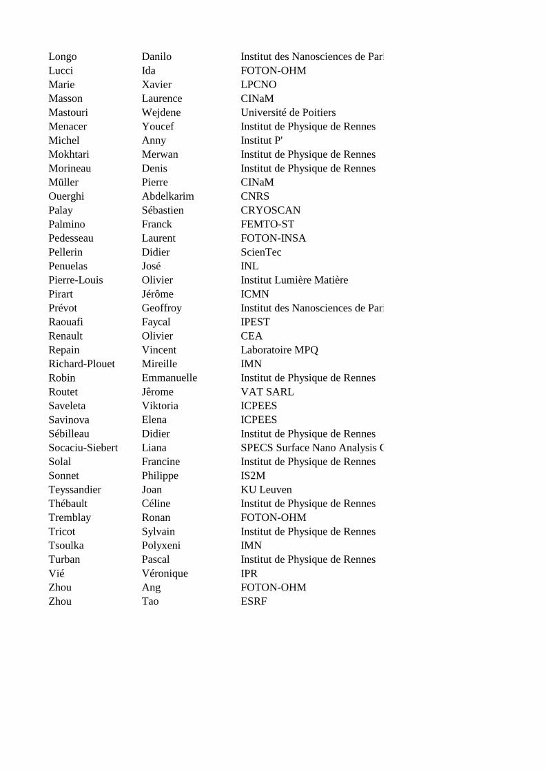
Longo Danilo Institut des Nanosciences de Paris
Lucci Ida FOTON-OHM
Marie Xavier LPCNO
Masson Laurence CINaM
Mastouri Wejdene Université de Poitiers
Menacer Youcef Institut de Physique de Rennes
Michel Anny Institut P'
Mokhtari Merwan Institut de Physique de Rennes
Morineau Denis Institut de Physique de Rennes
Müller Pierre CINaM
Ouerghi Abdelkarim CNRS
Palay Sébastien CRYOSCAN
Palmino Franck FEMTO-ST
Pedesseau Laurent FOTON-INSA
Pellerin Didier ScienTec
Penuelas José INL
Pierre-Louis Olivier Institut Lumière Matière
Pirart Jérôme ICMN
Prévot Geoffroy Institut des Nanosciences de Paris
Raouafi Faycal IPEST
Renault Olivier CEA
Repain Vincent Laboratoire MPQ
Richard-Plouet Mireille IMN
Robin Emmanuelle Institut de Physique de Rennes
Routet Jêrome VAT SARL
Saveleta Viktoria ICPEES
Savinova Elena ICPEES
Sébilleau Didier Institut de Physique de Rennes
Socaciu-Siebert Liana SPECS Surface Nano Analysis GmbH
Solal Francine Institut de Physique de Rennes
Sonnet Philippe IS2M
Teyssandier Joan KU Leuven
Thébault Céline Institut de Physique de Rennes
Tremblay Ronan FOTON-OHM
Tricot Sylvain Institut de Physique de Rennes
Tsoulka Polyxeni IMN
Turban Pascal Institut de Physique de Rennes
Vié Véronique IPR
Zhou Ang FOTON-OHM
Zhou Tao ESRF

Repas de Gala Jeudi 26 janvier à 20h30
Restaurant L’Amiral
2 Boulevard de la Tour d’Auvergne
Prendre le C4 à la sortie du Campus vers le centre-ville et descendre à l’arrêt Place de Bretagne
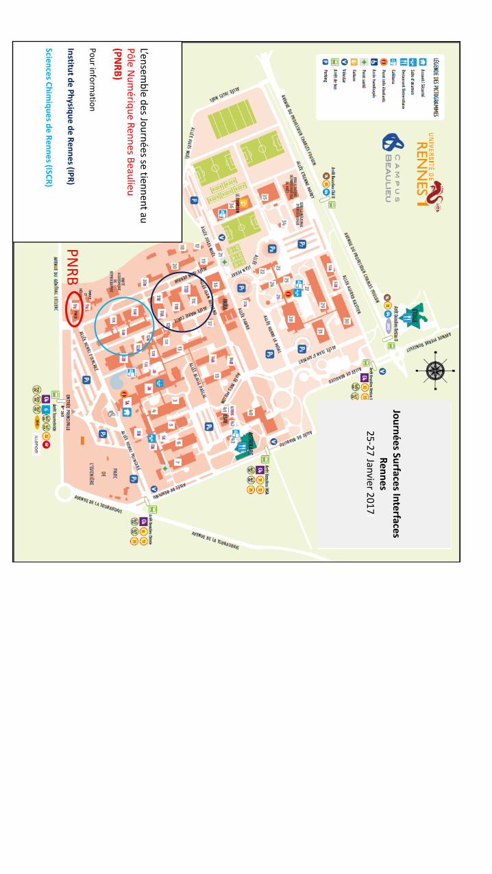
L’ensem
ble d
es Jou
rnée
s se tienn
en
t au
Pôle N
um
ériqu
e Ren
ne
s Beau
lieu
(PN
RB
)
Po
ur in
form
ation
Institu
t de
Ph
ysiqu
e d
e R
en
ne
s (IPR
)
Scien
ces C
him
iqu
es d
e R
en
ne
s (ISCR
)
Jou
rné
es Su
rfaces In
terfaces
Re
nn
es
25
-27
Janvier 2
01
7I
PN
RB

Heure Mercredi 25 Heure Jeudi 26 Heure Vendredi 27
Session 2 9h-12h30
Session 4 9h-12h30
09:00
Tao ZHOU
ESRF 09:00
Anne-Laure BIANCE
ILM
09:45 Anny MICHEL
Institut P’ 09:45 Matthieu BUGNET
MATEIS
10:30 Pause-café 10h30-11h
10:30 Pause-café 10h30-11h
11:00
Thomas JAOUEN
IPR et Univ. Fribourg 11:00
Fabrice COUSIN
LLB
11:45 Jacek
GONIAKOWSKI
INSP
11:45 Véronique VIE
IPR
12:00
Accueil 12h-14h
Hall PNRB
Buffet de
bienvenue 2ème étage
Espace co-working
12:30
Buffet 12h30-14h
2ème étage PNRB
Espace co-working
12:30
Buffet 12h30-14h
2ème étage
Espace co-working
Session 1 14h-18h15
Session 3 14h-16h15
14:00
Xavier MARIE
LPCNO 14:00 Elena SAVINOVA
ICPEES
14:45 Jérôme LAGOUTE
MPQ 14:45 Samy BOUKARI
IPCMS
15:30 Pause-café 15h30-16h
15:30 Mikaël KEPENEKIAN
ISCR
16:00
Christophe BRUN
INSP
16:15
Session Posters 16h15-19h30
16:45 Franck PALMINO
FEMSTO-ST
17:30
Laurence MASSON
CINaM
20:30
Dîner de Gala