Embed Size (px)
Citation preview
50 µA
S
ORVREFError Amp
To Internal Circutry
3 k�
5 k�
Reference Regulator
10
8
PWM Latch
S
R
2
1
9
6
3
12
15
7
OSC5
16
UVLO Lockout
4
Flip Flop
14
13
11
Output StageUC1525A
14
13
11
Output StageUC1527A
OR
OUTPUT B
OUTPUT A
VC
OUTPUT B
OUTPUT A
VC
NOR
NOR
VREFOSCOUT
+VIN
GROUND
SYNC
RT
CT
DISCHARGE
COMPENSATION
INV INPUT
NI INPUT
SOFTSTART
SHUTDOWN
Copyright © 2017, Texas Instruments Incorporated
Product
Folder
Order
Now
Technical
Documents
Tools &
Software
Support &Community
An IMPORTANT NOTICE at the end of this data sheet addresses availability, warranty, changes, use in safety-critical applications,intellectual property matters and other important disclaimers. PRODUCTION DATA.
UC1525A, UC1527A, UC2525AUC2527A, UC3525A, UC3527A
SLUS191D –FEBRUARY 1997–REVISED JULY 2017
UCx52xA Regulating Pulse Width Modulators
1
1 Features1• 8-V to 35-V Operation• 5.1-V Reference Trimmed to 1%• 100-Hz to 500-kHz Oscillator Range• Separate Oscillator Sync Terminal• Adjustable Dead-Time Control• Internal Soft Start• Pulse-by-Pulse Shutdown• Input Undervoltage Lockout With Hysteresis• Latching PWM to Prevent Multiple Pulses• Dual Source and Sink Output Drivers
2 Applications• Off-Line and DC/DC Power Supplies• Converters Using Voltage Mode• Single-Ended or Two-Switch Topology Designs• Solar Inverters• Welding Inverters• Motor Control• Battery Chargers
Block Diagram
3 DescriptionThe UC1525A/1527A series of pulse width modulatorintegrated circuits are designed to offer improvedperformance and lowered external parts count whenused in designing all types of switching powersupplies. The on-chip 5.1-V reference is trimmed to1% and the input common-mode range of the erroramplifier includes the reference voltage, eliminatingexternal resistors. A sync input to the oscillator allowsmultiple units to be slaved or a single unit to besynchronized to an external system clock. A singleresistor between CT and the discharge terminalsprovides a wide range of dead-time adjustment.These devices also feature built-in soft-start circuitrywith only an external timing capacitor required. Ashutdown terminal controls both the soft-start circuitryand the output stages, providing instantaneous turnoff through the PWM latch with pulsed shutdown, aswell as soft-start recycle with longer shutdowncommands.
Device Information(1)
PART NUMBER PACKAGE BODY SIZE (NOM)
UCx52xA
LCCC (20) 8.89 mm × 8.89 mmCDIP (16) 19.56 mm × 6.67 mmSOIC (16) 10.30 mm × 7.50 mmPDIP (16) 19.30 mm × 6.35 mmPLCC (20) 8.96 mm × 8.96 mm
(1) For all available packages, see the orderable addendum atthe end of the data sheet.
2
UC1525A, UC1527A, UC2525AUC2527A, UC3525A, UC3527ASLUS191D –FEBRUARY 1997–REVISED JULY 2017 www.ti.com
Product Folder Links: UC1525A UC1527A UC2525A UC2527A UC3525A UC3527A
Submit Documentation Feedback Copyright © 1997–2017, Texas Instruments Incorporated
Table of Contents1 Features .................................................................. 12 Applications ........................................................... 13 Description ............................................................. 14 Revision History..................................................... 25 Pin Configuration and Functions ......................... 36 Specifications......................................................... 4
6.1 Absolute Maximum Ratings ...................................... 46.2 ESD Ratings.............................................................. 46.3 Recommended Operating Conditions....................... 46.4 Thermal Information .................................................. 56.5 Electrical Characteristics........................................... 56.6 Typical Characteristics .............................................. 7
7 Detailed Description .............................................. 87.1 Overview ................................................................... 87.2 Functional Block Diagram ......................................... 87.3 Feature Description................................................... 9
7.4 Device Functional Modes.......................................... 98 Application and Implementation ........................ 10
8.1 Application Information............................................ 108.2 Typical Application ................................................. 10
9 Power Supply Recommendations ...................... 1610 Layout................................................................... 16
10.1 Layout Guidelines ................................................. 1610.2 Layout Example .................................................... 16
11 Device and Documentation Support ................. 1711.1 Documentation Support ....................................... 1711.2 Related Links ........................................................ 1711.3 Community Resources.......................................... 1711.4 Trademarks ........................................................... 1711.5 Electrostatic Discharge Caution............................ 1711.6 Glossary ................................................................ 17
12 Mechanical, Packaging, and OrderableInformation ........................................................... 17
4 Revision History
Changes from Revision C (January 2008) to Revision D Page
• Added ESD Ratings table, Feature Description section, Device Functional Modes, Application and Implementationsection, Power Supply Recommendations section, Layout section, Device and Documentation Support section, andMechanical, Packaging, and Orderable Information section ................................................................................................. 1
• Added Thermal Information table ........................................................................................................................................... 5• Changed RθJA values in the Thermal Information table: from 80-120 to N/A for J; from 90 to 47.6 for N; from 45-90 to
72.6 for DW; from 43-75 to 55.8 for FN; and from 70-80 to N/A for FK ................................................................................ 5• Changed RθJC values in the Thermal Information table: from 28 to 37.4 (top) and 10.1 (bottom) for J; from 45 to 37.3
(top) for N; from 25 to 34 (top) for DW; from 34 to 33.7 (top) for FN; and from 20 to 32.9 (top) to 3.5 (bottom) for FK ...... 5
4
5
6
7
8
SYNC
OSC Output
NC
CT
RT
NIIn
pu
t
INV
Inpu
t
NC
Co
mp
en
sa
tio
n
Sh
utd
ow
n+
VIN
Dis
ch
arg
e
So
ftS
tart
NC
VR
EF
9 10 11 12 13
3 2 1 20 1918
17
16
15
14
Output B
VC
NC
Ground
Output A
1
2
3
4
5
6
7
8
16
15
14
13
12
11
10
9
INV Input
NI Input
SYNC
OSC Output
CT
RT
Discharge
Soft Start
VREF
+VIN
Output B
VC
Ground
Output A
Shutdown
Compensation
3
UC1525A, UC1527A, UC2525AUC2527A, UC3525A, UC3527A
www.ti.com SLUS191D –FEBRUARY 1997–REVISED JULY 2017
Product Folder Links: UC1525A UC1527A UC2525A UC2527A UC3525A UC3527A
Submit Documentation FeedbackCopyright © 1997–2017, Texas Instruments Incorporated
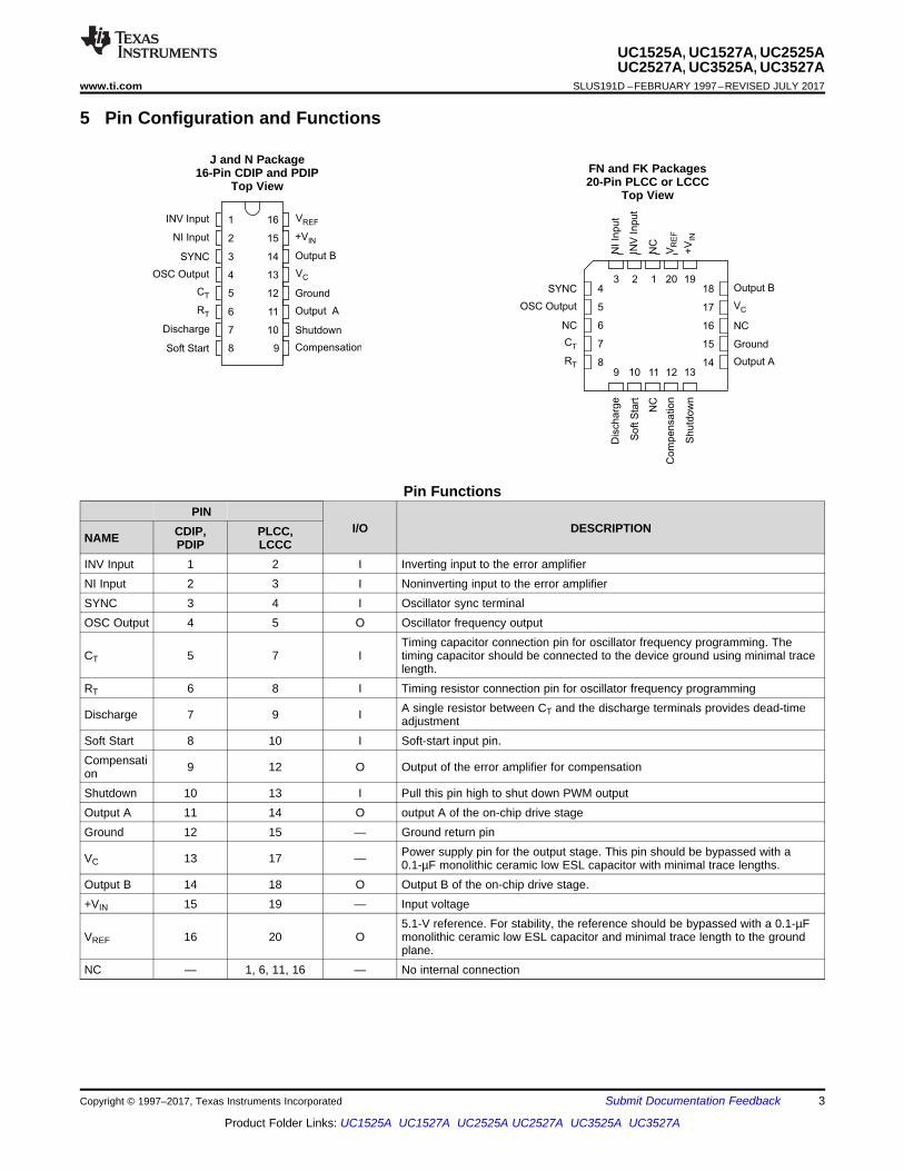
5 Pin Configuration and Functions
J and N Package16-Pin CDIP and PDIP
Top ViewFN and FK Packages20-Pin PLCC or LCCC
Top View
Pin FunctionsPIN
I/O DESCRIPTIONNAME CDIP,
PDIPPLCC,LCCC
INV Input 1 2 I Inverting input to the error amplifierNI Input 2 3 I Noninverting input to the error amplifierSYNC 3 4 I Oscillator sync terminalOSC Output 4 5 O Oscillator frequency output
CT 5 7 ITiming capacitor connection pin for oscillator frequency programming. Thetiming capacitor should be connected to the device ground using minimal tracelength.
RT 6 8 I Timing resistor connection pin for oscillator frequency programming
Discharge 7 9 I A single resistor between CT and the discharge terminals provides dead-timeadjustment
Soft Start 8 10 I Soft-start input pin.Compensation 9 12 O Output of the error amplifier for compensation
Shutdown 10 13 I Pull this pin high to shut down PWM outputOutput A 11 14 O output A of the on-chip drive stageGround 12 15 — Ground return pin
VC 13 17 — Power supply pin for the output stage. This pin should be bypassed with a0.1-µF monolithic ceramic low ESL capacitor with minimal trace lengths.
Output B 14 18 O Output B of the on-chip drive stage.+VIN 15 19 — Input voltage
VREF 16 20 O5.1-V reference. For stability, the reference should be bypassed with a 0.1-µFmonolithic ceramic low ESL capacitor and minimal trace length to the groundplane.
NC — 1, 6, 11, 16 — No internal connection
4
UC1525A, UC1527A, UC2525AUC2527A, UC3525A, UC3527ASLUS191D –FEBRUARY 1997–REVISED JULY 2017 www.ti.com
Product Folder Links: UC1525A UC1527A UC2525A UC2527A UC3525A UC3527A
Submit Documentation Feedback Copyright © 1997–2017, Texas Instruments Incorporated
(1) Stresses beyond those listed under Absolute Maximum Ratings may cause permanent damage to the device. These are stress ratingsonly, which do not imply functional operation of the device at these or any other conditions beyond those indicated under RecommendedOperating Conditions. Exposure to absolute-maximum-rated conditions for extended periods may affect device reliability.
6 Specifications
6.1 Absolute Maximum Ratingsover operating free-air temperature range (unless otherwise noted) (1)
MIN MAX UNIT+VIN Supply voltage 40 VVC Collector supply voltage 40 V
Logic inputs –0.3 5.5 VAnalog inputs –0.3 +VIN VOutput current, source or sink 500 mAReference output current 50 mAOscillator charging current 5 mAPower dissipation at TA = +25°C(2) 1000 mWPower dissipation at TC = +25°C(2) 2000 mWOperating junction temperature –55 150 °CLead temperature (soldering, 10 seconds) 300 °C
Tstg Storage temperature –65 150 °C
(1) JEDEC document JEP155 states that 500-V HBM allows safe manufacturing with a standard ESD control process.(2) JEDEC document JEP157 states that 250-V CDM allows safe manufacturing with a standard ESD control process.
6.2 ESD RatingsVALUE UNIT
V(ESD) Electrostatic dischargeHuman-body model (HBM), per ANSI/ESDA/JEDEC JS-001 (1) 3000
VCharged-device model (CDM), per JEDEC specification JESD22-C101 (2) 1500
6.3 Recommended Operating Conditionsover operating free-air temperature range (unless otherwise noted)
MIN MAX UNIT+VIN Input voltage 8 35 VVC Collector supply voltage 4.5 35 V
Sink/source load current (steady state) 0 100 mASink/source load current (peak) 0 400 mAReference load current 0 20 mAOscillator frequency range 100 400 HzOscillator timing resistor 2 150 kΩOscillator timing capacitor 0.001 0.01 µFDead time resistor range 0 500 Ω
Operating ambient temperatureUC1525A, UC1527A –55 125
°CUC2525A, UC2527A –25 85UC3525A, UC3527A 0 70
( )1
0.7 3T T D
fC R R
=+
5
UC1525A, UC1527A, UC2525AUC2527A, UC3525A, UC3527A
www.ti.com SLUS191D –FEBRUARY 1997–REVISED JULY 2017
Product Folder Links: UC1525A UC1527A UC2525A UC2527A UC3525A UC3527A
Submit Documentation FeedbackCopyright © 1997–2017, Texas Instruments Incorporated
(1) For more information about traditional and new thermal metrics, see the Semiconductor and IC Package Thermal Metrics applicationreport.
6.4 Thermal Information
THERMAL METRIC (1)
UCx52xA
UNITFK(LCCC)
J(CDIP)
DW(SOIC)
N(PDIP)
FN(PLCC)
20 PINS 16 PINS 16 PINS 16 PINS 20 PINSRθJA Junction-to-ambient thermal resistance N/A N/A 72.6 47.6 55.8 °C/WRθJC(top) Junction-to-case (top) thermal resistance 32.9 37.4 34 37.3 33.7 °C/WRθJB Junction-to-board thermal resistance 32.1 54.2 37.3 27.7 21.1 °C/WψJT Junction-to-top characterization parameter N/A N/A 8.9 17.3 9.7 °C/WψJB Junction-to-board characterization parameter N/A N/A 36.8 27.5 20.8 °C/WRθJC(bot) Junction-to-case (bottom) thermal resistance 3.5 10.1 N/A N/A N/A °C/W
(1) These parameters, although ensured over the recommended operating conditions, are not 100% tested in production.(2) Tested at fOSC = 40 kHz (RT = 3.6 kΩ, CT = 0.01 mF, RD = 0. Approximate oscillator frequency is defined by
.
6.5 Electrical Characteristicsover operating free-air temperature range (unless otherwise noted)
PARAMETER TEST CONDITIONS MIN TYP MAX UNITREFERENCE
Output voltage TJ = 25°CUC152xA,UC252xA 5.05 5.1 5.15
VUC352xA 5 5.1 5.2
Line regulation VIN = 8 V to 35 V 10 20 mVLoad regulation IL = 0 mA to 20 mA 20 50 mVTemperature stability (1) Over operating 20 50 mV
Total output variation (1) Line, load, and temperatureUC152xA,UC252xA 5 5.2
VUC352xA 4.95 5.25
Shorter circuit current VREF = 0, TJ = 25°C 80 100 mAOutput noise Voltage (1) 10 Hz ≤ 10 kHz, TJ = 25°C 40 200 µVrmsLong-term stability (1) TJ = 125°C 20 50 mVOSCILLATOR SECTION (2)
Initial accuracy (1) (2) TJ = 25°C 2% 6%
Voltage stability (1) (2) VIN = 8 V to 35 VUC152xA,UC252xA 0.3% 1%
UC352xA 1% 2%Temperature stability (1) Over operating 3% 6%Minimum frequency RT = 200 kΩ, CT = 0.1 mF 120 HzMaximum frequency RT = 2 kΩ, CT = 470 pF 400 kHzCurrent mirror IRT = 2 mA 1.7 2 2.2 mAClock amplitude (1) (2) 3 3.5 VClock width (1) (2) TJ = 25°C 0.3 0.5 1 µsSyncronization threshold (1) (2) 1.2 2 2.8 VSync input current Sync voltage = 3.5 V 1 2.5 mAERROR AMPLIFIER SECTION (VCM = 5.1 V)
Input offset voltageUC152xA, UC252xA 0.5 5 mVUC352xA 2 10
6
UC1525A, UC1527A, UC2525AUC2527A, UC3525A, UC3527ASLUS191D –FEBRUARY 1997–REVISED JULY 2017 www.ti.com
Product Folder Links: UC1525A UC1527A UC2525A UC2527A UC3525A UC3527A
Submit Documentation Feedback Copyright © 1997–2017, Texas Instruments Incorporated
Electrical Characteristics (continued)over operating free-air temperature range (unless otherwise noted)
PARAMETER TEST CONDITIONS MIN TYP MAX UNIT
(3) DC transconductance (gM) relates to DC open-loop voltage gain (AV) according to the following equation: AV = gMRL where RL is theresistance from pin 9 to ground. The minimum gM specification is used to calculate minimum AV when the error amplifier output isloaded.
(4) Tested at fOSC = 40 kHz (RT = 3.6 kΩ, CT = 0.01 mF, RD = 0 Ω.(5) These parameters, although ensured over the recommended operating conditions, are not 100% tested in production.(6) Collector off-state quiescent current measured at pin 13 with outputs low for UC1525A and high for UC1527A.
Input bias current 1 10µA
Input offset current 1DC open loop gain RL ≥ 10 MΩ 60 75 dBGain-bandwidth product (1) AV = 0 dB, TJ = 25°C 1 2 MHzDC transconductance (1) (3) TJ = 25°C, 30 kΩ ≤ RL ≤ 1 MΩ 1.1 1.5 mSLow-level output voltage 0.2 0.5
VHigh-level output voltage 3.8 5.6Common mode rejection VCM = 1.5 V to 5.2 V 60 75
dBSupply voltage rejection VIN = 8 V to 35 V 50 60PWM COMPARATORMinimum duty-cycle 0%Maximum duty-cycle 45% 49%
Input threshold (4) Zero duty-cycle 0.7 0.9V
Maximum duty-cycle 3.3 3.6Input bias current (4) 0.05 1 µASHUTDOWNSoft-start current VSD = 0 V, VSS = 0 V 25 50 80 µASoft-start low level VSD = 2.5 V 0.4 0.7
VShutdown threshold To outputs, VSS = 5.1 V, TJ = 25°C 0.6 0.8 1Shutdown input current VSD = 2.5 V 0.4 1 mAShutdown Delay (5) VSD = 2.5 V, TJ = 25°C 0.2 0.5 µSOUTPUT DRIVERS (EACH OUTPUT) (VC = 20 V)
Low-level output voltageISINK = 20 mA 0.2 0.4
VISINK = 100 mA 1 2
High-level output voltageISOURCE = 20 mA 18 19
VISOURCE = 100 mA 17 18
Undervoltage lockout VCOMP and VSS = High 6 7 8 VVC OFF current (6) VC = 35 V 200 µARise time (5) CL = 1 nF, TJ = 25°C 100 600
nsFall time (5) CL = 1 nF, TJ = 25°C 50 300TOTAL STANDBY CURRENTSupply current VIN = 35 V 14 20 mA
Minimum Recommended (RT - k:)
Max
imum
Rec
omm
ende
d R
D
2 4 6 8 10 120
100
200
300
400
500
D004
-55 qC 25 qC 125 qC
Frequency (Hz)
Ope
n-Lo
op V
olta
ge G
ain
(dB
)
Ope
n-Lo
op P
hase
(q)
-20 -400
0 -200
20 0
40 200
60 400
80 600
100 800
10 100 1k 10k 100k 1M 10M
D005
Voltage GainRL = 30 k:RL = 100 k:RL = 300 k:RL = 1 M:
RL = fVoltage PhasePhase
Charge Time (Ps)
Dea
d T
ime
Res
ista
nce
(:)
0.1 1 10 100 2000
100
200
300
400
500
D003
CT = 0.1 PFCT = .05 PFCT = .02 PFCT = .01 PFCT = 5 nFCT = 2 nFCT = 1 nF
Charge Time (s)
Tim
ing
Res
ista
nce
(k:
)
0.0002
0.001
0.01
0.1
1
10
100200
1P 10P 100P 1m 10m 100m
D002
CT = 0.01 PFCT = 0.05 PFCT = 0.02 PFCT = 0.1 PFCT = 5 nFCT = 2 nFCT = 1 nF
7
UC1525A, UC1527A, UC2525AUC2527A, UC3525A, UC3527A
www.ti.com SLUS191D –FEBRUARY 1997–REVISED JULY 2017
Product Folder Links: UC1525A UC1527A UC2525A UC2527A UC3525A UC3527A
Submit Documentation FeedbackCopyright © 1997–2017, Texas Instruments Incorporated
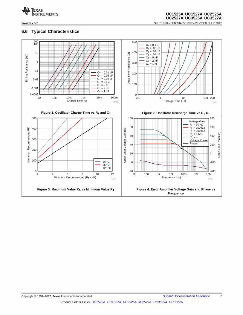
6.6 Typical Characteristics
Figure 1. Oscillator Charge Time vs RT and CT Figure 2. Oscillator Discharge Time vs RT CT
Figure 3. Maximum Value RD vs Minimum Value RT Figure 4. Error Amplifier Voltage Gain and Phase vsFrequency
50 µA
S
ORVREFError Amp
To Internal Circutry
3 k�
5 k�
Reference Regulator
10
8
PWM Latch
S
R
2
1
9
6
3
12
15
7
OSC5
16
UVLO Lockout
4
Flip Flop
14
13
11
Output StageUC1525A
14
13
11
Output StageUC1527A
OR
OUTPUT B
OUTPUT A
VC
OUTPUT B
OUTPUT A
VC
NOR
NOR
VREFOSCOUT
+VIN
GROUND
SYNC
RT
CT
DISCHARGE
COMPENSATION
INV INPUT
NI INPUT
SOFTSTART
SHUTDOWN
Copyright © 2017, Texas Instruments Incorporated
8
UC1525A, UC1527A, UC2525AUC2527A, UC3525A, UC3527ASLUS191D –FEBRUARY 1997–REVISED JULY 2017 www.ti.com
Product Folder Links: UC1525A UC1527A UC2525A UC2527A UC3525A UC3527A
Submit Documentation Feedback Copyright © 1997–2017, Texas Instruments Incorporated
7 Detailed Description
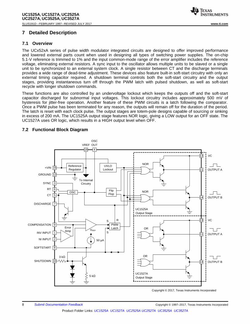
7.1 OverviewThe UCx52xA series of pulse width modulator integrated circuits are designed to offer improved performanceand lowered external parts count when used in designing all types of switching power supplies. The on-chip5.1-V reference is trimmed to 1% and the input common-mode range of the error amplifier includes the referencevoltage, eliminating external resistors. A sync input to the oscillator allows multiple units to be slaved or a singleunit to be synchronized to an external system clock. A single resistor between CT and the discharge terminalsprovides a wide range of dead-time adjustment. These devices also feature built-in soft-start circuitry with only anexternal timing capacitor required. A shutdown terminal controls both the soft-start circuitry and the outputstages, providing instantaneous turn off through the PWM latch with pulsed shutdown, as well as soft-startrecycle with longer shutdown commands.
These functions are also controlled by an undervoltage lockout which keeps the outputs off and the soft-startcapacitor discharged for subnormal input voltages. This lockout circuitry includes approximately 500 mV ofhysteresis for jitter-free operation. Another feature of these PWM circuits is a latch following the comparator.Once a PWM pulse has been terminated for any reason, the outputs will remain off for the duration of the period.The latch is reset with each clock pulse. The output stages are totem-pole designs capable of sourcing or sinkingin excess of 200 mA. The UC1525A output stage features NOR logic, giving a LOW output for an OFF state. TheUC1527A uses OR logic, which results in a HIGH output level when OFF.
7.2 Functional Block Diagram
9
UC1525A, UC1527A, UC2525AUC2527A, UC3525A, UC3527A
www.ti.com SLUS191D –FEBRUARY 1997–REVISED JULY 2017
Product Folder Links: UC1525A UC1527A UC2525A UC2527A UC3525A UC3527A
Submit Documentation FeedbackCopyright © 1997–2017, Texas Instruments Incorporated
7.3 Feature Description
7.3.1 Adjustable Dead-Time ControlA single resistor between CT and the discharge terminals provides a wide range of dead-time adjustment.
7.3.2 Soft StartSoft start is achieved by connecting the soft-start pin to ground through a capacitor, charged by the 50-µAcurrent source. See Functional Block Diagram.
7.3.3 Input Undervoltage Lockout With HysteresisThe undervoltage lockout keeps the outputs off and the soft-start capacitor discharged for subnormal inputvoltages. This lockout circuitry includes approximately 500 mV of hysteresis for jitter-free operation.
7.3.4 Shutdown and Pulse-by-Pulse Current LimitingSee Shutdown Options (See Functional Block Diagram).
7.4 Device Functional ModesThis device has no functional modes.
7.4.1 Shutdown Options (See Functional Block Diagram)Since both the compensation and soft-start terminals have current source pullups, either can readily accept apull-down signal which only has to sink a maximum of 100 A to turn off the outputs. This is subject to the addedrequirement of discharging whatever external capacitance may be attached to these pins.
An alternate approach is the use of the shutdown circuitry of the shutdown pin which has been improved toenhance the available shutdown options. Activating this circuit by applying a positive signal on the shutdown pinperforms two functions; the PWM latch is immediately set providing the fastest turn-off signal to the outputs; anda 150-A current sink begins to discharge the external soft-start capacitor. If the shutdown command is short, thePWM signal is terminated without significant discharge of the soft-start capacitor, thus, allowing, for example, aconvenient implementation of pulse-by-pulse current limiting. Holding the shutdown pin high for a longer duration,however, will ultimately discharge this external capacitor, recycling slow turnon upon release.
The shutdown pin should not be left floating as noise pickup could conceivably interrupt normal operation. Alltransitions of the voltage on the shutdown pin should be within the time frame of one clock cycle and notrepeated at a frequency higher than 10 clock cycles.
VREF
PWM
Adj.
3 kW
10 kW
1.5 kW
3.6 kW
.009
0.1
1 = VOS
2 = I ( + )
3 = I ( − )
Clock
SYNC
RT
Ramp
100 W
.001
10 kW 0.1
Oscill
ato
r
16
4
3
Flip/Flop
E/A
D.U.T.
Out A
1 k, 1 W
(2)
Out B
Soft-Start
50 Am
5 kW
5 kW
0.1
6
CT
Deadtime
7
5Comp
9
V/I Meter
−
+
1
2
3
1
2
3
1
2
3
1
2
3
1
2
PWM
ReferenceRegulator 15
13
11
12
8
10
14
+VIN
0.1
A
B
5 kW
VREF
Shutdown
5 Fm
+
GND
VC
0.1
Copyright © 2017, Texas Instruments Incorporated
10
UC1525A, UC1527A, UC2525AUC2527A, UC3525A, UC3527ASLUS191D –FEBRUARY 1997–REVISED JULY 2017 www.ti.com
Product Folder Links: UC1525A UC1527A UC2525A UC2527A UC3525A UC3527A
Submit Documentation Feedback Copyright © 1997–2017, Texas Instruments Incorporated
8 Application and Implementation
NOTEInformation in the following applications sections is not part of the TI componentspecification, and TI does not warrant its accuracy or completeness. TI’s customers areresponsible for determining suitability of components for their purposes. Customers shouldvalidate and test their design implementation to confirm system functionality.
8.1 Application InformationThe UC1525A/1527A series of pulse width modulator integrated circuits are designed to offer improvedperformance and lowered external parts count when used in designing all types of switching power supplies. TheUC1525A output stage features NOR logic, giving a LOW output for an OFF state. The UC1527A utilizes ORlogic which results in a HIGH output level when OFF.
8.2 Typical Application
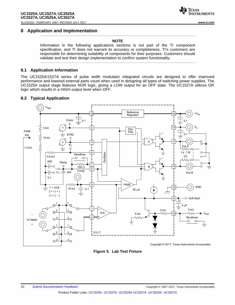
Figure 5. Lab Test Fixture
VREF
RT
CT
16
Q1 Q5 Q8
7.4 kW
Q36
5 Q6 Q9
2 kW 14 kW
Ramp To PWM
Blanking To Outout
Q12
Q10 Q11
Q13 3 kW 250 kW
Clock
Q1425 kW
1 kW
2 kW
400 Am5 pF
Q7
Q4
Q2
1 kW
3
7
12
SYNC
DISCHARGE
GND
23 kW
4
12
Q2
Q1
+VC A
B
UC1525A
GND
+VSUPPLY
Return
R1
30 W
R2
C1T1
11
14C2
T2
13
11
UC1525A, UC1527A, UC2525AUC2527A, UC3525A, UC3527A
www.ti.com SLUS191D –FEBRUARY 1997–REVISED JULY 2017
Product Folder Links: UC1525A UC1527A UC2525A UC2527A UC3525A UC3527A
Submit Documentation FeedbackCopyright © 1997–2017, Texas Instruments Incorporated
Typical Application (continued)8.2.1 Theory of Operation
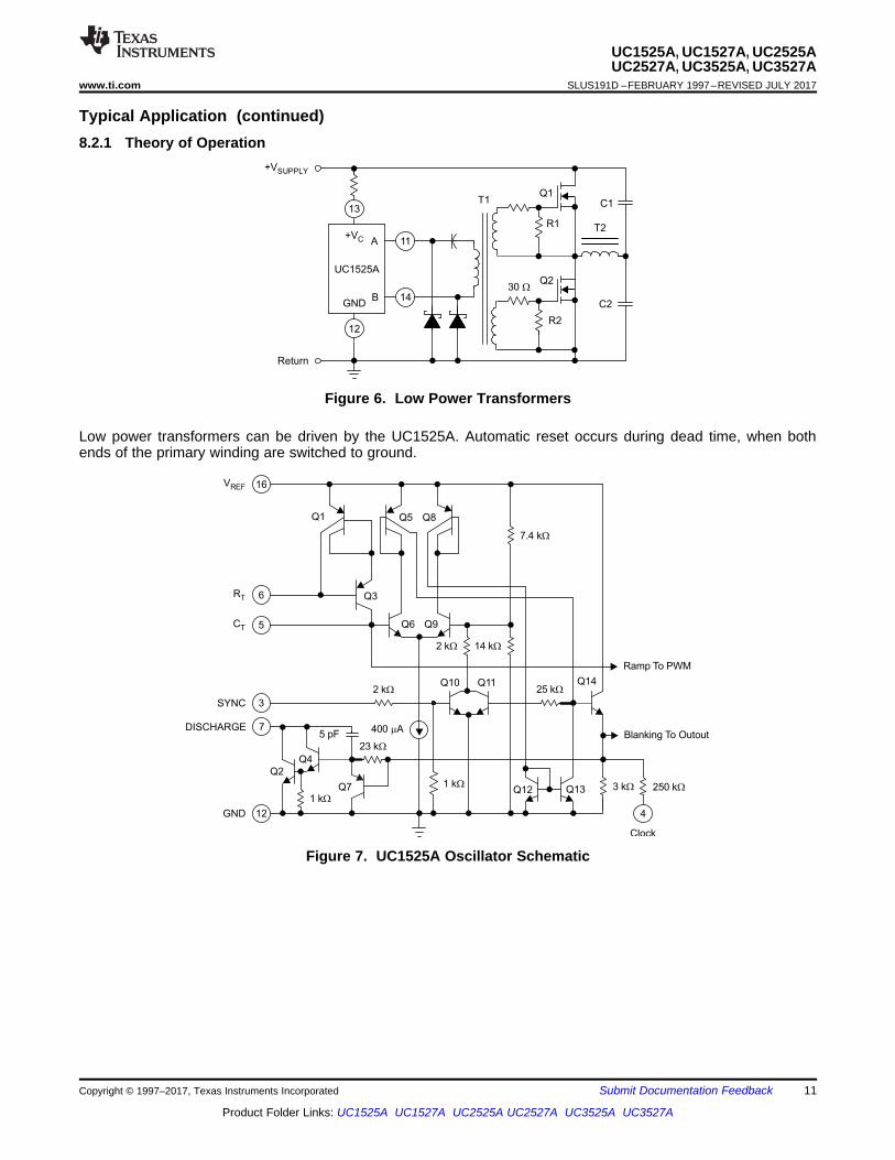
Figure 6. Low Power Transformers
Low power transformers can be driven by the UC1525A. Automatic reset occurs during dead time, when bothends of the primary winding are switched to ground.
Figure 7. UC1525A Oscillator Schematic
+VSUPPLYQ1 To Output Filter
R2R1
13
11
14
12
+VCA
B
UC1525A
GND
Return
13+VIN
Q5
Q4
+VREF
Q6
Q3Q2Q1
5 kW 10 kW 10 kW
1114
Output
2 kW
Q8
Q9
Q7
Q10
Q11
Q6 OmmittedIn UC1527A
+VC
Clock F/F PWM
5 K
+VIN15
Q3
Q4
Q2Q1
1
2
Inv Input
NI Input
200 Am5.8 V 100 W
Comp9
to PWM
Comparator
100 Am
12
UC1525A, UC1527A, UC2525AUC2527A, UC3525A, UC3527ASLUS191D –FEBRUARY 1997–REVISED JULY 2017 www.ti.com
Product Folder Links: UC1525A UC1527A UC2525A UC2527A UC3525A UC3527A
Submit Documentation Feedback Copyright © 1997–2017, Texas Instruments Incorporated
Typical Application (continued)
Figure 8. UC1525A Error Amplifier
Figure 9. UC1525A Output Circuit (1/2 circuit shown)
Figure 10. Grounded Driver Outputs For Single-Ended Supplies
13
11
14
12
Q2
Q1+V
CA
B
UC1525A
GND
+VSUPPLY
Return
R1
C1
R2
C2
R3
T1
+15 V
13
11
14
12
D1
D2
Return
30 W
30 W
Q2
Q1 T1
D1, D2: UC3611
+V CA
B
UC1525A
GND
13
UC1525A, UC1527A, UC2525AUC2527A, UC3525A, UC3527A
www.ti.com SLUS191D –FEBRUARY 1997–REVISED JULY 2017
Product Folder Links: UC1525A UC1527A UC2525A UC2527A UC3525A UC3527A
Submit Documentation FeedbackCopyright © 1997–2017, Texas Instruments Incorporated
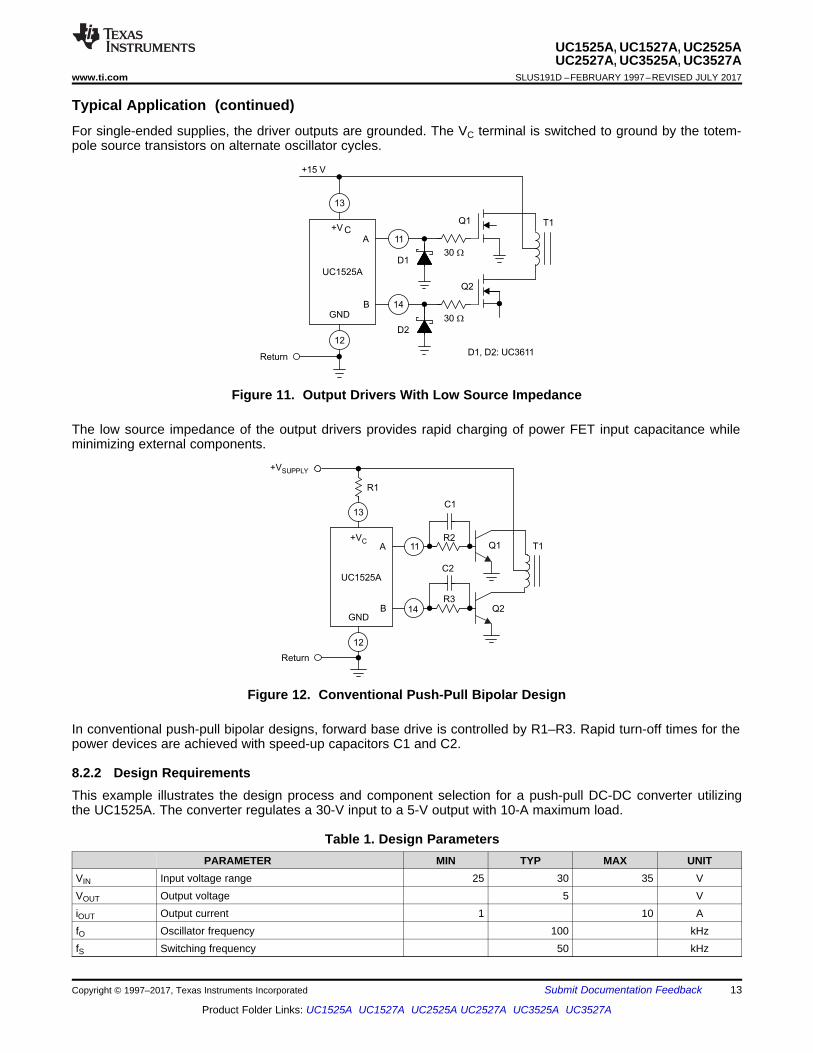
Typical Application (continued)For single-ended supplies, the driver outputs are grounded. The VC terminal is switched to ground by the totem-pole source transistors on alternate oscillator cycles.
Figure 11. Output Drivers With Low Source Impedance
The low source impedance of the output drivers provides rapid charging of power FET input capacitance whileminimizing external components.
Figure 12. Conventional Push-Pull Bipolar Design
In conventional push-pull bipolar designs, forward base drive is controlled by R1–R3. Rapid turn-off times for thepower devices are achieved with speed-up capacitors C1 and C2.
8.2.2 Design RequirementsThis example illustrates the design process and component selection for a push-pull DC-DC converter utilizingthe UC1525A. The converter regulates a 30-V input to a 5-V output with 10-A maximum load.
Table 1. Design ParametersPARAMETER MIN TYP MAX UNIT
VIN Input voltage range 25 30 35 VVOUT Output voltage 5 ViOUT Output current 1 10 AfO Oscillator frequency 100 kHzfS Switching frequency 50 kHz
OUT F OUT FO
L SW IN(max)
V V N (V V )1L ( ) 11.57 H
I f 2 2 V� u �
u � P' u u
LIM IN(min)MAX
OUT F
2 D V 2 0.35 25VN 3.3
V V 5V 0.3V
u u u u
� �
T T D
1f
C (0.7 R 3 R )
�
14
UC1525A, UC1527A, UC2525AUC2527A, UC3525A, UC3527ASLUS191D –FEBRUARY 1997–REVISED JULY 2017 www.ti.com
Product Folder Links: UC1525A UC1527A UC2525A UC2527A UC3525A UC3527A
Submit Documentation Feedback Copyright © 1997–2017, Texas Instruments Incorporated
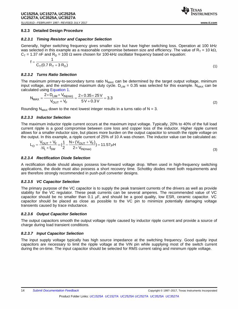
8.2.3 Detailed Design Procedure
8.2.3.1 Timing Resistor and Capacitor SelectionGenerally, higher switching frequency gives smaller size but have higher switching loss. Operation at 100 kHzwas selected in this example as a reasonable compromise between size and efficiency. The value of RT = 10 kΩ,CT = 1.37 nF and RD = 100 Ω were chosen for 100-kHz oscillator frequency based on equation:
(1)
8.2.3.2 Turns Ratio SelectionThe maximum primary-to-secondary turns ratio NMAX can be determined by the target output voltage, minimuminput voltage, and the estimated maximum duty cycle. DLIM = 0.35 was selected for this example. NMAX can becalculated using Equation 1.
(2)
Rounding NMAX down to the next lowest integer results in a turns ratio of N = 3.
8.2.3.3 Inductor SelectionThe maximum inductor ripple current occurs at the maximum input voltage. Typically, 20% to 40% of the full loadcurrent ripple is a good compromise between core loss and copper loss of the inductor. Higher ripple currentallows for a smaller inductor size, but places more burden on the output capacitor to smooth the ripple voltage onthe output. In this example, a ripple current of 25% of 10 A was chosen. The inductor value can be calculated as:
(3)
8.2.3.4 Rectification Diode SelectionA rectification diode should always possess low-forward voltage drop. When used in high-frequency switchingapplications, the diode must also possess a short recovery time. Schottky diodes meet both requirements andare therefore strongly recommended in push-pull converter designs.
8.2.3.5 VC Capacitor SelectionThe primary purpose of the VC capacitor is to supply the peak transient currents of the drivers as well as providestability for the VC regulator. These peak currents can be several amperes. The recommended value of VCcapacitor should be no smaller than 0.1 μF, and should be a good quality, low ESR, ceramic capacitor. VCcapacitor should be placed as close as possible to the VC pin to minimize potentially damaging voltagetransients caused by trace inductance.
8.2.3.6 Output Capacitor SelectionThe output capacitors smooth the output voltage ripple caused by inductor ripple current and provide a source ofcharge during load transient conditions.
8.2.3.7 Input Capacitor SelectionThe input supply voltage typically has high source impedance at the switching frequency. Good quality inputcapacitors are necessary to limit the ripple voltage at the VIN pin while supplying most of the switch currentduring the on-time. The input capacitor should be selected for RMS current rating and minimum ripple voltage.
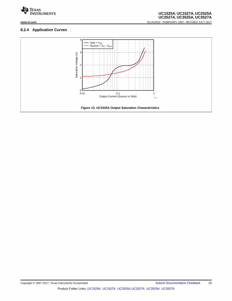
Output Current (Source or Sink)
Sat
urat
ion
Vol
tage
(V
)
0.01 0.1 10
1
2
3
4
D001
Sink = VOLSource = VO - VOH
15
UC1525A, UC1527A, UC2525AUC2527A, UC3525A, UC3527A
www.ti.com SLUS191D –FEBRUARY 1997–REVISED JULY 2017
Product Folder Links: UC1525A UC1527A UC2525A UC2527A UC3525A UC3527A
Submit Documentation FeedbackCopyright © 1997–2017, Texas Instruments Incorporated
8.2.4 Application Curves
Figure 13. UC1525A Output Saturation Characteristics
FB
SHUTDOWN
OUTA
VC
Vin
OUTB
1
xx
xxxx
1 xxx
2
xxxx
xx
2xx
1
xx
xxxx
INV
NI
SYNC
OSC
CT
RT
DISCHARGE
SS
VREF
+VIN
OUTB
VC
GND
OUTA
SHUTDOWN
xx C
VC
xxCSS
xxxx
RD
xxxxRTxxxxCT
UC1525A
1
xx
xxxxxxCP
12
xx
xx
xxCz
12
xxxx
xxxxxx
Rz
COMP
12
xxxx
xxxxxx
RFB
1
xxxx
2
xxxxxxxx
CV
RE
F
2xx
1
xxxx
xxxxx RB
1
xxxx
xxxxxxRA
xx C
VIN
16
UC1525A, UC1527A, UC2525AUC2527A, UC3525A, UC3527ASLUS191D –FEBRUARY 1997–REVISED JULY 2017 www.ti.com
Product Folder Links: UC1525A UC1527A UC2525A UC2527A UC3525A UC3527A
Submit Documentation Feedback Copyright © 1997–2017, Texas Instruments Incorporated
9 Power Supply RecommendationsThe voltage range for VIN is 8 V to 35 V.
The voltage range for VC is 4.5 V to 35 V. Choose a voltage level which is suitable for the power switch, forexample, 12 V for MOSFET.
10 Layout
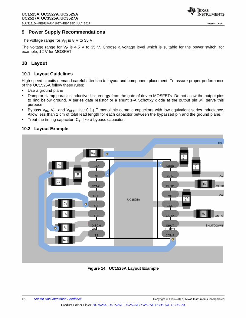
10.1 Layout GuidelinesHigh-speed circuits demand careful attention to layout and component placement. To assure proper performanceof the UC1525A follow these rules:• Use a ground plane• Damp or clamp parasitic inductive kick energy from the gate of driven MOSFETs. Do not allow the output pins
to ring below ground. A series gate resistor or a shunt 1-A Schottky diode at the output pin will serve thispurpose.
• Bypass VIN, VC, and VREF. Use 0.1-µF monolithic ceramic capacitors with low equivalent series inductance.Allow less than 1 cm of total lead length for each capacitor between the bypassed pin and the ground plane.
• Treat the timing capacitor, CT, like a bypass capacitor.
10.2 Layout Example
Figure 14. UC1525A Layout Example
17
UC1525A, UC1527A, UC2525AUC2527A, UC3525A, UC3527A
www.ti.com SLUS191D –FEBRUARY 1997–REVISED JULY 2017
Product Folder Links: UC1525A UC1527A UC2525A UC2527A UC3525A UC3527A
Submit Documentation FeedbackCopyright © 1997–2017, Texas Instruments Incorporated
11 Device and Documentation Support
11.1 Documentation Support
11.1.1 Related DocumentationFor related documentation see the following:
Switching Power Supply Topology Voltage Mode vs Current Mode (SLUA119)
11.2 Related LinksThe table below lists quick access links. Categories include technical documents, support and communityresources, tools and software, and quick access to sample or buy.
Table 2. Related Links
PARTS PRODUCT FOLDER SAMPLE & BUY TECHNICALDOCUMENTS
TOOLS &SOFTWARE
SUPPORT &COMMUNITY
UC1525A Click here Click here Click here Click here Click hereUC1527A Click here Click here Click here Click here Click hereUC2525A Click here Click here Click here Click here Click hereUC2527A Click here Click here Click here Click here Click hereUC3525A Click here Click here Click here Click here Click hereUC3527A Click here Click here Click here Click here Click here
11.3 Community ResourcesThe following links connect to TI community resources. Linked contents are provided "AS IS" by the respectivecontributors. They do not constitute TI specifications and do not necessarily reflect TI's views; see TI's Terms ofUse.
TI E2E™ Online Community TI's Engineer-to-Engineer (E2E) Community. Created to foster collaborationamong engineers. At e2e.ti.com, you can ask questions, share knowledge, explore ideas and helpsolve problems with fellow engineers.
Design Support TI's Design Support Quickly find helpful E2E forums along with design support tools andcontact information for technical support.
11.4 TrademarksE2E is a trademark of Texas Instruments.All other trademarks are the property of their respective owners.
11.5 Electrostatic Discharge CautionThese devices have limited built-in ESD protection. The leads should be shorted together or the device placed in conductive foamduring storage or handling to prevent electrostatic damage to the MOS gates.
11.6 GlossarySLYZ022 — TI Glossary.
This glossary lists and explains terms, acronyms, and definitions.
12 Mechanical, Packaging, and Orderable InformationThe following pages include mechanical, packaging, and orderable information. This information is the mostcurrent data available for the designated devices. This data is subject to change without notice and revision ofthis document. For browser-based versions of this data sheet, refer to the left-hand navigation.
PACKAGE OPTION ADDENDUM
www.ti.com 1-Sep-2018
Addendum-Page 1
PACKAGING INFORMATION
Orderable Device Status(1)
Package Type PackageDrawing
Pins PackageQty
Eco Plan(2)
Lead/Ball Finish(6)
MSL Peak Temp(3)
Op Temp (°C) Device Marking(4/5)
Samples
5962-89511032A ACTIVE LCCC FK 20 1 TBD POST-PLATE N / A for Pkg Type -55 to 125 5962-89511032AUC1525AL/883B
5962-8951103EA ACTIVE CDIP J 16 1 TBD A42 N / A for Pkg Type -55 to 125 5962-8951103EAUC1525AJ/883B
5962-8951104EA ACTIVE CDIP J 16 1 TBD A42 N / A for Pkg Type -55 to 125 5962-8951104EAUC1527AJ/883B
UC1525AJ ACTIVE CDIP J 16 25 TBD A42 N / A for Pkg Type -55 to 125 UC1525AJ
UC1525AJ883B ACTIVE CDIP J 16 1 TBD A42 N / A for Pkg Type -55 to 125 5962-8951103EAUC1525AJ/883B
UC1525AL ACTIVE LCCC FK 20 1 TBD POST-PLATE N / A for Pkg Type -55 to 125 UC1525AL
UC1525AL883B ACTIVE LCCC FK 20 1 TBD POST-PLATE N / A for Pkg Type -55 to 125 5962-89511032AUC1525AL/883B
UC1527AJ ACTIVE CDIP J 16 1 TBD A42 N / A for Pkg Type -55 to 125 UC1527AJ
UC1527AJ883B ACTIVE CDIP J 16 1 TBD A42 N / A for Pkg Type -55 to 125 5962-8951104EAUC1527AJ/883B
UC2525ADW ACTIVE SOIC DW 16 40 Green (RoHS& no Sb/Br)
CU NIPDAU Level-2-260C-1 YEAR -25 to 85 UC2525ADW
UC2525ADWTR ACTIVE SOIC DW 16 2000 Green (RoHS& no Sb/Br)
CU NIPDAU Level-2-260C-1 YEAR -25 to 85 UC2525ADW
UC2525AJ ACTIVE CDIP J 16 1 TBD A42 N / A for Pkg Type -25 to 85 UC2525AJ
UC2525AN ACTIVE PDIP N 16 25 Green (RoHS& no Sb/Br)
CU NIPDAU | Call TI N / A for Pkg Type -25 to 85 UC2525AN
UC2525ANG4 ACTIVE PDIP N 16 25 Green (RoHS& no Sb/Br)
Call TI N / A for Pkg Type -25 to 85 UC2525AN
UC2525BDW ACTIVE SOIC DW 16 40 Green (RoHS& no Sb/Br)
CU NIPDAU Level-2-260C-1 YEAR -25 to 85 UC2525BDW
UC2525BN ACTIVE PDIP N 16 25 Green (RoHS& no Sb/Br)
CU NIPDAU | Call TI N / A for Pkg Type -25 to 85 UC2525BN
PACKAGE OPTION ADDENDUM
www.ti.com 1-Sep-2018
Addendum-Page 2
Orderable Device Status(1)
Package Type PackageDrawing
Pins PackageQty
Eco Plan(2)
Lead/Ball Finish(6)
MSL Peak Temp(3)
Op Temp (°C) Device Marking(4/5)
Samples
UC2527AN ACTIVE PDIP N 16 25 Green (RoHS& no Sb/Br)
CU NIPDAU | Call TI N / A for Pkg Type -40 to 85 UC2527AN
UC3525ADW ACTIVE SOIC DW 16 40 Green (RoHS& no Sb/Br)
CU NIPDAU Level-2-260C-1 YEAR 0 to 70 UC3525ADW
UC3525ADWG4 ACTIVE SOIC DW 16 40 Green (RoHS& no Sb/Br)
CU NIPDAU Level-2-260C-1 YEAR 0 to 70 UC3525ADW
UC3525ADWTR ACTIVE SOIC DW 16 2000 Green (RoHS& no Sb/Br)
CU NIPDAU Level-2-260C-1 YEAR 0 to 70 UC3525ADW
UC3525ADWTRG4 ACTIVE SOIC DW 16 2000 Green (RoHS& no Sb/Br)
CU NIPDAU Level-2-260C-1 YEAR 0 to 70 UC3525ADW
UC3525AJ ACTIVE CDIP J 16 1 TBD A42 N / A for Pkg Type 0 to 70 UC3525AJ
UC3525AN ACTIVE PDIP N 16 25 Green (RoHS& no Sb/Br)
CU NIPDAU N / A for Pkg Type 0 to 70 UC3525AN
UC3525ANG4 ACTIVE PDIP N 16 25 Green (RoHS& no Sb/Br)
CU NIPDAU N / A for Pkg Type 0 to 70 UC3525AN
UC3527AN ACTIVE PDIP N 16 25 Green (RoHS& no Sb/Br)
CU NIPDAU N / A for Pkg Type 0 to 70 UC3527AN
UC3527ANG4 ACTIVE PDIP N 16 25 Green (RoHS& no Sb/Br)
CU NIPDAU N / A for Pkg Type 0 to 70 UC3527AN
(1) The marketing status values are defined as follows:ACTIVE: Product device recommended for new designs.LIFEBUY: TI has announced that the device will be discontinued, and a lifetime-buy period is in effect.NRND: Not recommended for new designs. Device is in production to support existing customers, but TI does not recommend using this part in a new design.PREVIEW: Device has been announced but is not in production. Samples may or may not be available.OBSOLETE: TI has discontinued the production of the device.
(2) RoHS: TI defines "RoHS" to mean semiconductor products that are compliant with the current EU RoHS requirements for all 10 RoHS substances, including the requirement that RoHS substancedo not exceed 0.1% by weight in homogeneous materials. Where designed to be soldered at high temperatures, "RoHS" products are suitable for use in specified lead-free processes. TI mayreference these types of products as "Pb-Free".RoHS Exempt: TI defines "RoHS Exempt" to mean products that contain lead but are compliant with EU RoHS pursuant to a specific EU RoHS exemption.Green: TI defines "Green" to mean the content of Chlorine (Cl) and Bromine (Br) based flame retardants meet JS709B low halogen requirements of <=1000ppm threshold. Antimony trioxide basedflame retardants must also meet the <=1000ppm threshold requirement.
(3) MSL, Peak Temp. - The Moisture Sensitivity Level rating according to the JEDEC industry standard classifications, and peak solder temperature.
(4) There may be additional marking, which relates to the logo, the lot trace code information, or the environmental category on the device.
PACKAGE OPTION ADDENDUM
www.ti.com 1-Sep-2018
Addendum-Page 3
(5) Multiple Device Markings will be inside parentheses. Only one Device Marking contained in parentheses and separated by a "~" will appear on a device. If a line is indented then it is a continuationof the previous line and the two combined represent the entire Device Marking for that device.
(6) Lead/Ball Finish - Orderable Devices may have multiple material finish options. Finish options are separated by a vertical ruled line. Lead/Ball Finish values may wrap to two lines if the finishvalue exceeds the maximum column width.
Important Information and Disclaimer:The information provided on this page represents TI's knowledge and belief as of the date that it is provided. TI bases its knowledge and belief on informationprovided by third parties, and makes no representation or warranty as to the accuracy of such information. Efforts are underway to better integrate information from third parties. TI has taken andcontinues to take reasonable steps to provide representative and accurate information but may not have conducted destructive testing or chemical analysis on incoming materials and chemicals.TI and TI suppliers consider certain information to be proprietary, and thus CAS numbers and other limited information may not be available for release.
In no event shall TI's liability arising out of such information exceed the total purchase price of the TI part(s) at issue in this document sold by TI to Customer on an annual basis.
OTHER QUALIFIED VERSIONS OF UC1525A, UC1527A, UC2525A, UC2525AM, UC3525A, UC3525AM, UC3527A :
• Catalog: UC3525A, UC3527A, UC2525A, UC3525AM, UC3525A
• Military: UC2525AM, UC1525A, UC1525A, UC1527A
NOTE: Qualified Version Definitions:
• Catalog - TI's standard catalog product
• Military - QML certified for Military and Defense Applications
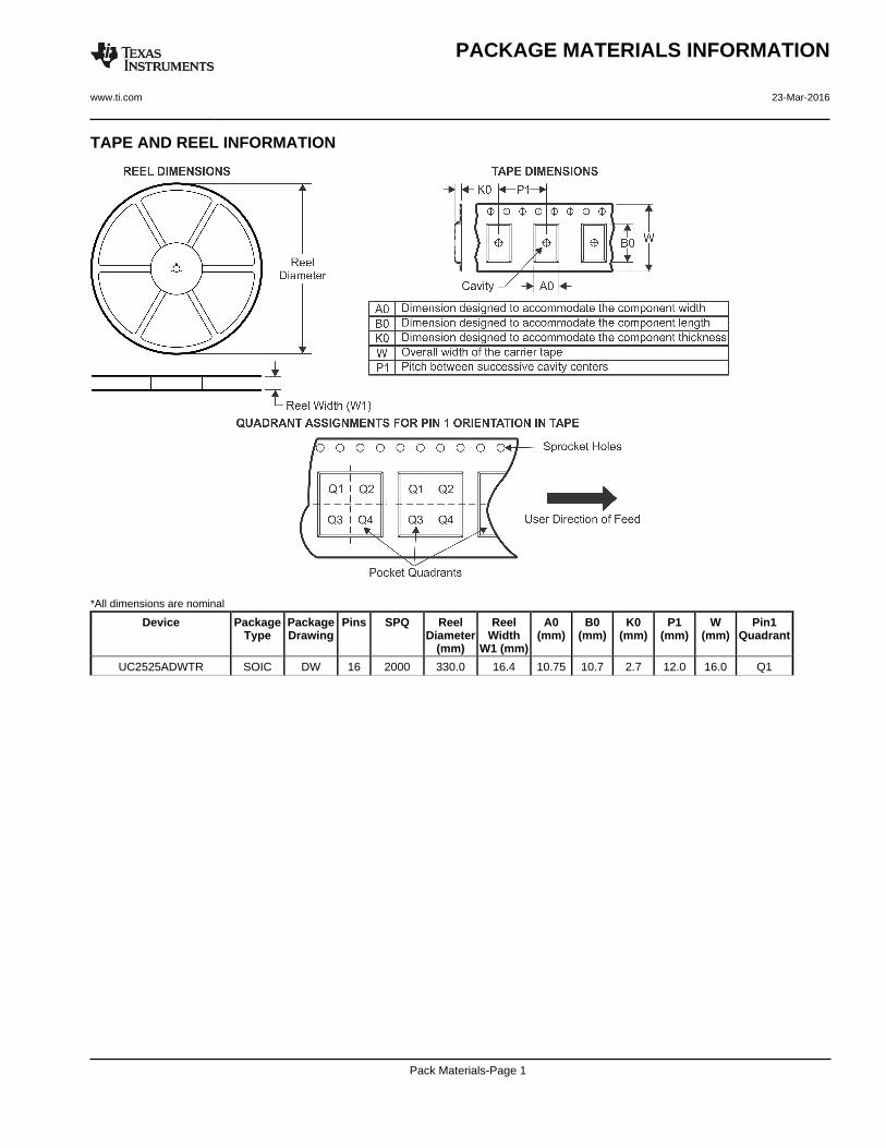
TAPE AND REEL INFORMATION
*All dimensions are nominal
Device PackageType
PackageDrawing
Pins SPQ ReelDiameter
(mm)
ReelWidth
W1 (mm)
A0(mm)
B0(mm)
K0(mm)
P1(mm)
W(mm)
Pin1Quadrant
UC2525ADWTR SOIC DW 16 2000 330.0 16.4 10.75 10.7 2.7 12.0 16.0 Q1
PACKAGE MATERIALS INFORMATION
www.ti.com 23-Mar-2016
Pack Materials-Page 1
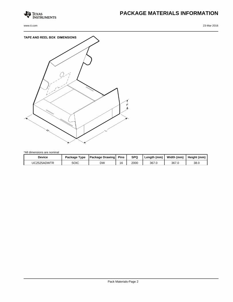
*All dimensions are nominal
Device Package Type Package Drawing Pins SPQ Length (mm) Width (mm) Height (mm)
UC2525ADWTR SOIC DW 16 2000 367.0 367.0 38.0
PACKAGE MATERIALS INFORMATION
www.ti.com 23-Mar-2016
Pack Materials-Page 2
IMPORTANT NOTICE
Texas Instruments Incorporated (TI) reserves the right to make corrections, enhancements, improvements and other changes to itssemiconductor products and services per JESD46, latest issue, and to discontinue any product or service per JESD48, latest issue. Buyersshould obtain the latest relevant information before placing orders and should verify that such information is current and complete.TI’s published terms of sale for semiconductor products (http://www.ti.com/sc/docs/stdterms.htm) apply to the sale of packaged integratedcircuit products that TI has qualified and released to market. Additional terms may apply to the use or sale of other types of TI products andservices.Reproduction of significant portions of TI information in TI data sheets is permissible only if reproduction is without alteration and isaccompanied by all associated warranties, conditions, limitations, and notices. TI is not responsible or liable for such reproduceddocumentation. Information of third parties may be subject to additional restrictions. Resale of TI products or services with statementsdifferent from or beyond the parameters stated by TI for that product or service voids all express and any implied warranties for theassociated TI product or service and is an unfair and deceptive business practice. TI is not responsible or liable for any such statements.Buyers and others who are developing systems that incorporate TI products (collectively, “Designers”) understand and agree that Designersremain responsible for using their independent analysis, evaluation and judgment in designing their applications and that Designers havefull and exclusive responsibility to assure the safety of Designers' applications and compliance of their applications (and of all TI productsused in or for Designers’ applications) with all applicable regulations, laws and other applicable requirements. Designer represents that, withrespect to their applications, Designer has all the necessary expertise to create and implement safeguards that (1) anticipate dangerousconsequences of failures, (2) monitor failures and their consequences, and (3) lessen the likelihood of failures that might cause harm andtake appropriate actions. Designer agrees that prior to using or distributing any applications that include TI products, Designer willthoroughly test such applications and the functionality of such TI products as used in such applications.TI’s provision of technical, application or other design advice, quality characterization, reliability data or other services or information,including, but not limited to, reference designs and materials relating to evaluation modules, (collectively, “TI Resources”) are intended toassist designers who are developing applications that incorporate TI products; by downloading, accessing or using TI Resources in anyway, Designer (individually or, if Designer is acting on behalf of a company, Designer’s company) agrees to use any particular TI Resourcesolely for this purpose and subject to the terms of this Notice.TI’s provision of TI Resources does not expand or otherwise alter TI’s applicable published warranties or warranty disclaimers for TIproducts, and no additional obligations or liabilities arise from TI providing such TI Resources. TI reserves the right to make corrections,enhancements, improvements and other changes to its TI Resources. TI has not conducted any testing other than that specificallydescribed in the published documentation for a particular TI Resource.Designer is authorized to use, copy and modify any individual TI Resource only in connection with the development of applications thatinclude the TI product(s) identified in such TI Resource. NO OTHER LICENSE, EXPRESS OR IMPLIED, BY ESTOPPEL OR OTHERWISETO ANY OTHER TI INTELLECTUAL PROPERTY RIGHT, AND NO LICENSE TO ANY TECHNOLOGY OR INTELLECTUAL PROPERTYRIGHT OF TI OR ANY THIRD PARTY IS GRANTED HEREIN, including but not limited to any patent right, copyright, mask work right, orother intellectual property right relating to any combination, machine, or process in which TI products or services are used. Informationregarding or referencing third-party products or services does not constitute a license to use such products or services, or a warranty orendorsement thereof. Use of TI Resources may require a license from a third party under the patents or other intellectual property of thethird party, or a license from TI under the patents or other intellectual property of TI.TI RESOURCES ARE PROVIDED “AS IS” AND WITH ALL FAULTS. TI DISCLAIMS ALL OTHER WARRANTIES ORREPRESENTATIONS, EXPRESS OR IMPLIED, REGARDING RESOURCES OR USE THEREOF, INCLUDING BUT NOT LIMITED TOACCURACY OR COMPLETENESS, TITLE, ANY EPIDEMIC FAILURE WARRANTY AND ANY IMPLIED WARRANTIES OFMERCHANTABILITY, FITNESS FOR A PARTICULAR PURPOSE, AND NON-INFRINGEMENT OF ANY THIRD PARTY INTELLECTUALPROPERTY RIGHTS. TI SHALL NOT BE LIABLE FOR AND SHALL NOT DEFEND OR INDEMNIFY DESIGNER AGAINST ANY CLAIM,INCLUDING BUT NOT LIMITED TO ANY INFRINGEMENT CLAIM THAT RELATES TO OR IS BASED ON ANY COMBINATION OFPRODUCTS EVEN IF DESCRIBED IN TI RESOURCES OR OTHERWISE. IN NO EVENT SHALL TI BE LIABLE FOR ANY ACTUAL,DIRECT, SPECIAL, COLLATERAL, INDIRECT, PUNITIVE, INCIDENTAL, CONSEQUENTIAL OR EXEMPLARY DAMAGES INCONNECTION WITH OR ARISING OUT OF TI RESOURCES OR USE THEREOF, AND REGARDLESS OF WHETHER TI HAS BEENADVISED OF THE POSSIBILITY OF SUCH DAMAGES.Unless TI has explicitly designated an individual product as meeting the requirements of a particular industry standard (e.g., ISO/TS 16949and ISO 26262), TI is not responsible for any failure to meet such industry standard requirements.Where TI specifically promotes products as facilitating functional safety or as compliant with industry functional safety standards, suchproducts are intended to help enable customers to design and create their own applications that meet applicable functional safety standardsand requirements. Using products in an application does not by itself establish any safety features in the application. Designers mustensure compliance with safety-related requirements and standards applicable to their applications. Designer may not use any TI products inlife-critical medical equipment unless authorized officers of the parties have executed a special contract specifically governing such use.Life-critical medical equipment is medical equipment where failure of such equipment would cause serious bodily injury or death (e.g., lifesupport, pacemakers, defibrillators, heart pumps, neurostimulators, and implantables). Such equipment includes, without limitation, allmedical devices identified by the U.S. Food and Drug Administration as Class III devices and equivalent classifications outside the U.S.TI may expressly designate certain products as completing a particular qualification (e.g., Q100, Military Grade, or Enhanced Product).Designers agree that it has the necessary expertise to select the product with the appropriate qualification designation for their applicationsand that proper product selection is at Designers’ own risk. Designers are solely responsible for compliance with all legal and regulatoryrequirements in connection with such selection.Designer will fully indemnify TI and its representatives against any damages, costs, losses, and/or liabilities arising out of Designer’s non-compliance with the terms and provisions of this Notice.
Mailing Address: Texas Instruments, Post Office Box 655303, Dallas, Texas 75265Copyright © 2018, Texas Instruments Incorporated
Mouser Electronics
Authorized Distributor
Click to View Pricing, Inventory, Delivery & Lifecycle Information: Texas Instruments:
UC2527AN UC2527ANG4


![Autour de la libpcap [width=.8]tcpdump](https://img.pdfslide.fr/doc/110x75/62771ffe49c9482abb60005c/autour-de-la-libpcap-width8tcpdump.jpg)