86 CANADIAN JOURNAL OF ELECTRICAL AND COMPUTER ENGINEERING, VOL. 37, NO. 2, SPRING 2014
A High-Throughput VLSI Architecture forReal-Time Optical OFDM SystemsWith an Efficient Phase Equalizer
Architecture d’ITGE à haut-débit à pour lessystèmes optique à temps réel OFDM avec
un égaliseur de phase efficaceReza Ghanaatian, Mahdi Shabany, and Morteza H. Shoreh
Abstract— In this paper, a novel high-throughput very large scale integrated circuit architecture for areal-time implementation of intensity modulation direct detection optical orthogonal frequency divisionmultiplexing system is proposed, achieving the highest throughput reported to date. The proposedarchitecture utilizes a fast, pipelined, and parallel inverse fast Fourier transform/fast Fourier transformin the transmitter/receiver, which is customized to satisfy the throughput requirements of the advancedoptical systems. In addition, an efficient high-accuracy equalization method is developed, improving thesystem performance compared with the conventional linear equalizers. To evaluate the system performance,the OptiSystem software is used to model the optical channel and a Virtex-6 ML-605 evaluation boardis used as the implementation platform. Moreover, the synthesis results in a 180-nm CMOS technologyprove that the proposed architecture achieves a sustained throughput of 22.5 Gb/s with a 4.89-mm2 corearea.
Résumé— Dans ce papier, une architecture de circuit intégré à très grande échelle (ITGE) et haut débit estproposée pour une nouvelle mise en œuvre d’un système à temps réel de modulation d’intensité optiqueorthogonale pour la détection directe de la fréquence des systèmes de multiplexage, permettant ainsid’atteindre de plus haut débit jusqu’à nos jour. L’architecture proposée utilise une transformée de Fourierrapide (Fast Fourier Transform, FFT) inversée, en pipeline, et parallèle dans l’émetteur/récepteur. Cettedernière a été adaptée afin de satisfaire les contraintes de débit des systèmes optiques de pointe. Également,un procédé d’égalisation de haute précision efficace est développé, ce qui améliore les performances dusystème par rapport aux égaliseurs linéaires classiques. Pour évaluer les performances du système, lelogiciel OptiSystem est utilisé pour modéliser le canal optique et une carte d’évaluation Virtex-6 ML-605est utilisée comme plate-forme de développement. De plus, les résultats de la synthèse avec une technologieCMOS de 180 nm prouvent que l’architecture proposée permet d’obtenir un débit soutenu de 22.5 Gb/savec une puce microélectronique de 4.89 mm2.
Index Terms— Efficient phase equalizer, intensity modulation direct detection (IMDD), optical orthogonalfrequency-division multiplexing (OOFDM), throughput, very large scale integrated circuit (VLSI)architecture.
I. INTRODUCTION
ORTHOGONAL frequency-division multiplexing(OFDM) is widely used in both wired and wireless
systems due to its various advantages, such as the spectralefficiency, great performance in multipath fading channels,and the simple hardware implementation [1]. Recently, ithas become the technology of choice for systems employingoptical communications [2]. The tremendous increase in
Manuscript received August 26, 2013; revised January 6, 2014 and March 2,2014; accepted April 3, 2014. Date of current version August 15, 2014.
The authors are with the Department of Electrical Engineering,Sharif University of Technology, Tehran 11369, Iran (e-mail:[email protected]; [email protected]; [email protected]).
Associate Editor managing this paper’s review: Reza Heidari.Color versions of one or more of the figures in this paper are available
online at http://ieeexplore.ieee.org.Digital Object Identifier 10.1109/CJECE.2014.2317756
demand for the network capacity due to the advent ofnew Internet applications, and the development in digitalsignal processing (DSP) technology, which enables theimplementation of sophisticated OFDM signal processingalgorithms, has created a great motive to use OFDM inoptical communication systems [3].
Among optical OFDM (OOFDM) systems, the coherentoptical OFDM provides the ultimate performance on thereceiver sensitivity, spectral efficiency, and robustness againstdispersion [4]. On the other hand, the direct detection opti-cal OFDM (DD-OOFDM) systems come with a lower cost,appealing to various applications [4]. Intensity modulationdirect detection OOFDM (IMDD-OOFDM) is one type ofDD-OOFDM system, which is a promising solution towarddeveloping high-bandwidth access networks. This is mainlybecause of the fact that IMDD-OOFDM offers a reasonable
0840-8688 © 2014 IEEE. Personal use is permitted, but republication/redistribution requires IEEE permission.See http://www.ieee.org/publications_standards/publications/rights/index.html for more information.
GHANAATIAN et al.: HIGH-THROUGHPUT VLSI ARCHITECTURE FOR REAL-TIME OPTICAL OFDM SYSTEMS 87
reduction in the overall network complexity. Meanwhile, theexperimental demonstration of a real-time IMDD-OOFDMtransceiver is vital to enable the practical realization of theOFDM systems in next-generation optical networks. How-ever, the implementation of an OOFDM system has variouschallenges including devising a high-throughput hardwarearchitecture, which could handle the parallel, complex, andcomputationally intense OFDM signal processing algorithms.The real-time implementation of OOFDM systems has beenpreviously studied in [5]–[7]. However, an efficient architec-ture for the baseband part of the system at extremely high datarates is still a major challenge.
In this paper, a real-time, high-throughput very largescale integrated circuit (VLSI) implementation of anIMDD-OOFDM transceiver is proposed, which provides greatperformance for the system via taking advantage of a highspeed, an efficient FFT, and a low-complexity symbol syn-chronizer in the transceiver. In addition to the above con-tribution, an efficient yet simple phase equalizer is devel-oped based on the nature of the optical channels, provid-ing better channel estimation. This effectively enhances thesystem performance compared with the conventional equal-ization approaches. The rest of this paper is organized asfollows. In Section II, the OOFDM system architecture isreviewed and the proposed hardware architecture for the real-time implementation is discussed. The transmission perfor-mance and the implementation results are demonstrated inSections III and IV, respectively. Finally, Section V concludesthis paper.
II. REAL-TIME OOFDM TRANSCEIVER ARCHITECTURE
A. System Model
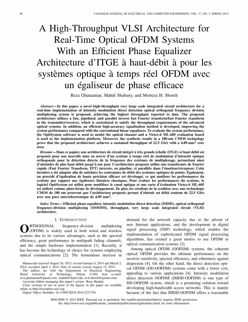
Fig. 1 shows the block diagram of a real-time DD-OOFDMtransceiver. On the transmitter side, the parallel input data aremapped onto the constellation points using an M-quadratic-amplitude modulation (QAM), and then fed to a 32-pointparallel IFFT core. To generate real valued samples for theintensity modulator, only half of the subcarriers are used fordata (one zero component at the dc subcarrier and othersfor data), while others are left for their complex conjugate.A cyclic prefix (CP) of eight samples is used resulting ina 40 samples OFDM symbol. The real OFDM electricalsignal is then fed into a Mach–Zehnder modulator (MZM)to modulate the laser intensity. Following the modulator, anerbium-doped fiber amplifier (EDFA) is utilized to adjustthe optical launch power to measure the bit-error-rate (BER)performance. Finally, the optical signal is transmitted throughthe optical link (see Section III for more details).
On the receiver side, an EDFA is used to amplify thereceived signal power followed by a simple photodetector toperform the direct detection. The samples of the convertedphotocurrent are then fed to the OFDM receiver, where thesymbol synchronizer, the FFT, the channel equalizer, and thedemodulator recover data in each subcarrier (Fig. 1).
With respect to the architecture in Fig. 1, in this paper, theOFDM transmitter and receiver are implemented on a XilinxVirtex-6 Field-programmable gate array (FPGA) (see Section
Fig. 1. Block diagram of the proposed real-time DD-OOFDM system.
IV for details). The OptiSystem is used for the simulationof the optical channel and other optical devices used in thesystem. The OFDM symbols are saved and imported to thesoftware and the output of the channel is exported, and fed tothe FPGA.
B. Optical OFDM System Description
1) Symbol Synchronization: The symbol synchronizationis one of the essential blocks at the receiver in an OFDMsystem, which plays an important role in the overall systemperformance. For the purpose of the symbol synchronization,one task is to find the symbol start. The conventional methodto estimate the OFDM symbol start is using the correlationconcept. Considering an OFDM symbol y(n), the correlationof this signal with its shifted version can be defined as
γ (n) =δ+Ng+1∑
i=δ
y(n + i) y∗(n + N + i) (1)
where N represents the number of FFT points, Ng is thelength of the CP region, and δ shows the initial random offsetof the receiving OFDM samples. The result of the abovecorrelation is maximized when the correlation is calculatedin the CP region. This means by detecting the peak absolutevalue of γ , the beginning of the symbol can be found.
It can be shown that the performance of the above methoddeteriorates in noisy environments as well as in cases wherethe FFT size is small, such as OOFDM systems. Therefore,in this paper, it is proposed to use a folding technique wherethe value of γ is added to its shifted version with the lengthof OFDM symbol as follows:
γk[n] = 1
k
k−1∑
i=0
γ [n − i Ns] (2)
for example, the five order of folding can be derived as
γ5[n] = 1
5{γ [n] + γ [n − Ns] + γ [n − 2Ns]+ γ [n − 3Ns] + γ [n − 4Ns]} (3)
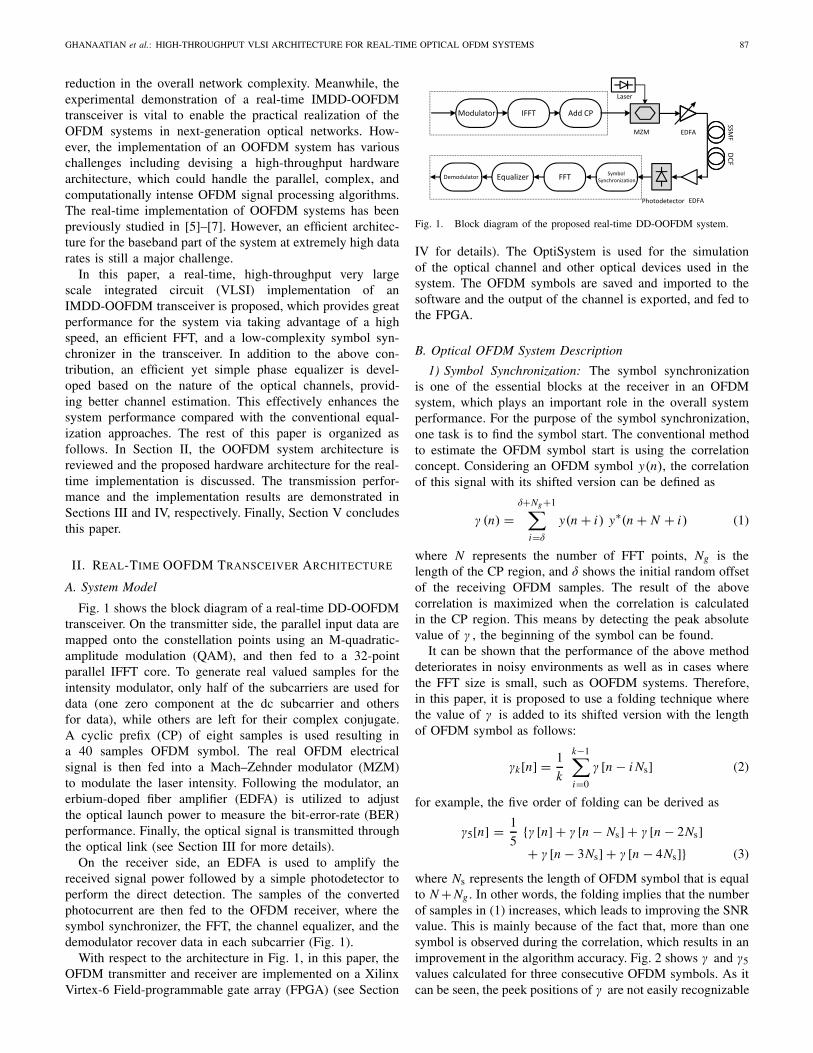
where Ns represents the length of OFDM symbol that is equalto N + Ng . In other words, the folding implies that the numberof samples in (1) increases, which leads to improving the SNRvalue. This is mainly because of the fact that, more than onesymbol is observed during the correlation, which results in animprovement in the algorithm accuracy. Fig. 2 shows γ and γ5values calculated for three consecutive OFDM symbols. As itcan be seen, the peek positions of γ are not easily recognizable
88 CANADIAN JOURNAL OF ELECTRICAL AND COMPUTER ENGINEERING, VOL. 37, NO. 2, SPRING 2014
Fig. 2. Calculated values for three consecutive OFDM symbols. (a) γ value. (b) γ5 value.
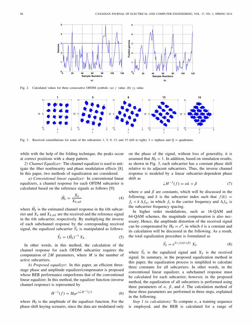
Fig. 3. Received constellations for some of the subcarriers 1, 5, 9, 13, and 15 (left to right). I = inphase and Q = quadrature.
while with the help of the folding technique, the peaks occurat correct positions with a sharp pattern.
2) Channel Equalizer: The channel equalizer is used to mit-igate the fiber nonlinearity and phase modulation effects [8].In this paper, two methods of equalization are considered.
a) Conventional linear equalizer: In conventional linearequalizers, a channel response for each OFDM subcarrier iscalculated based on the reference signals as follows [9]:
Hk = Xk
Xk,ref(4)
where Hk is the estimated channel response in the kth subcar-rier and Xk and Xk,ref are the received and the reference signalin the kth subcarrier, respectively. By multiplying the inverseof each subchannel response by the corresponding receivedsignal, the equalized subcarrier Yk is manipulated as follows:
Yk = (Hk)−1 Xk . (5)
In other words, in this method, the calculation of thechannel response for each OFDM subcarrier requires thecomputation of 2M parameters, where M is the number ofactive subcarriers.
b) Proposed equalizer: In this paper, an efficient three-stage phase and amplitude equalizer/compensator is proposedwhose BER performance outperforms that of the conventionallinear equalizer. In this method, the equalizer function (inversechannel response) is represented by
H −1( f ) = H0e j � H−1( f ) (6)
where H0 is the amplitude of the equalizer function. For thephase-shift keying scenario, since the data are modulated only
on the phase of the signal, without loss of generality, it isassumed that H0 = 1. In addition, based on simulation results,as shown in Fig. 3, each subcarrier has a constant phase shiftrelative to its adjacent subcarriers. Thus, the inverse channelresponse is modeled by a linear subcarrier-dependent phaseshift as
� H −1( f ) = αk + β (7)
where α and β are constants, which will be discussed in thefollowing, and k is the subcarrier index such that f (k) =fc + k � fsc, in which fc is the carrier frequency and � fsc isthe subcarrier frequency spacing.
In higher order modulations, such as 16-QAM and64-QAM schemes, the magnitude compensation is also nec-essary. Hence, the amplitude distortion of the received signalcan be compensated by H0 = eδ, in which δ is a constant andits calculation will be discussed in the following. As a result,the total equalization procedure is formulated as
Yk = eδ+ j (αk+β) Xk (8)
where Yk is the equalized signal and Xk is the receivedsignal. In summary, in the proposed equalization method inthis paper, the equalization process is simplified to calculatethree constants for all subcarriers. In other words, in theconventional linear equalizer, a subchannel response mustbe calculated for each subcarrier; however, in the proposedmethod, the equalization of all subcarriers is performed usingthree parameters of α, β, and δ. The calculation method ofthese three parameters are performed in three steps, explainedin the following.
Step 1 (α calculation): To compute α, a training sequenceis employed, and the BER is calculated for a range of
GHANAATIAN et al.: HIGH-THROUGHPUT VLSI ARCHITECTURE FOR REAL-TIME OPTICAL OFDM SYSTEMS 89
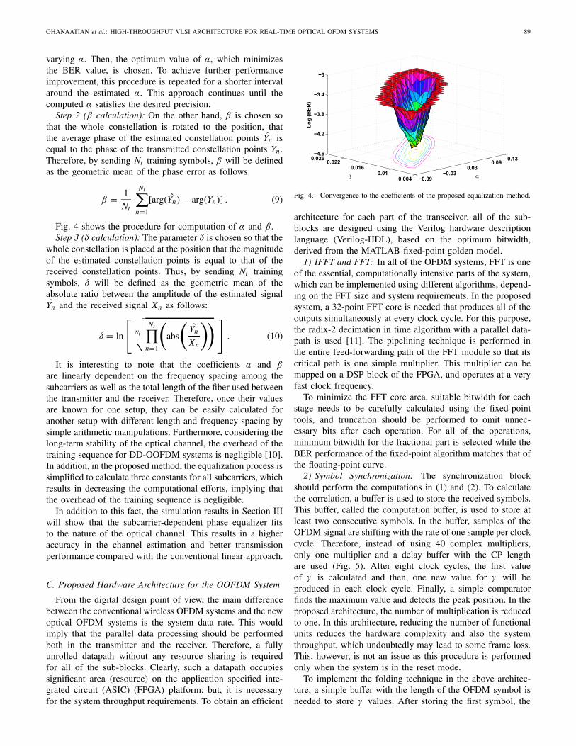
varying α. Then, the optimum value of α, which minimizesthe BER value, is chosen. To achieve further performanceimprovement, this procedure is repeated for a shorter intervalaround the estimated α. This approach continues until thecomputed α satisfies the desired precision.
Step 2 (β calculation): On the other hand, β is chosen sothat the whole constellation is rotated to the position, thatthe average phase of the estimated constellation points Yn isequal to the phase of the transmitted constellation points Yn .Therefore, by sending Nt training symbols, β will be definedas the geometric mean of the phase error as follows:
β = 1
Nt
Nt∑
n=1
[arg(Yn) − arg(Yn)] . (9)
Fig. 4 shows the procedure for computation of α and β.Step 3 (δ calculation): The parameter δ is chosen so that the
whole constellation is placed at the position that the magnitudeof the estimated constellation points is equal to that of thereceived constellation points. Thus, by sending Nt trainingsymbols, δ will be defined as the geometric mean of theabsolute ratio between the amplitude of the estimated signalYn and the received signal Xn as follows:
δ = ln
⎡
⎣ Nt
√√√√Nt∏
n=1
(abs
(Yn
Xn
)) ⎤
⎦ . (10)
It is interesting to note that the coefficients α and βare linearly dependent on the frequency spacing among thesubcarriers as well as the total length of the fiber used betweenthe transmitter and the receiver. Therefore, once their valuesare known for one setup, they can be easily calculated foranother setup with different length and frequency spacing bysimple arithmetic manipulations. Furthermore, considering thelong-term stability of the optical channel, the overhead of thetraining sequence for DD-OOFDM systems is negligible [10].In addition, in the proposed method, the equalization process issimplified to calculate three constants for all subcarriers, whichresults in decreasing the computational efforts, implying thatthe overhead of the training sequence is negligible.
In addition to this fact, the simulation results in Section IIIwill show that the subcarrier-dependent phase equalizer fitsto the nature of the optical channel. This results in a higheraccuracy in the channel estimation and better transmissionperformance compared with the conventional linear approach.
C. Proposed Hardware Architecture for the OOFDM System
From the digital design point of view, the main differencebetween the conventional wireless OFDM systems and the newoptical OFDM systems is the system data rate. This wouldimply that the parallel data processing should be performedboth in the transmitter and the receiver. Therefore, a fullyunrolled datapath without any resource sharing is requiredfor all of the sub-blocks. Clearly, such a datapath occupiessignificant area (resource) on the application specified inte-grated circuit (ASIC) (FPGA) platform; but, it is necessaryfor the system throughput requirements. To obtain an efficient
Fig. 4. Convergence to the coefficients of the proposed equalization method.
architecture for each part of the transceiver, all of the sub-blocks are designed using the Verilog hardware descriptionlanguage (Verilog-HDL), based on the optimum bitwidth,derived from the MATLAB fixed-point golden model.
1) IFFT and FFT: In all of the OFDM systems, FFT is oneof the essential, computationally intensive parts of the system,which can be implemented using different algorithms, depend-ing on the FFT size and system requirements. In the proposedsystem, a 32-point FFT core is needed that produces all of theoutputs simultaneously at every clock cycle. For this purpose,the radix-2 decimation in time algorithm with a parallel data-path is used [11]. The pipelining technique is performed inthe entire feed-forwarding path of the FFT module so that itscritical path is one simple multiplier. This multiplier can bemapped on a DSP block of the FPGA, and operates at a veryfast clock frequency.
To minimize the FFT core area, suitable bitwidth for eachstage needs to be carefully calculated using the fixed-pointtools, and truncation should be performed to omit unnec-essary bits after each operation. For all of the operations,minimum bitwidth for the fractional part is selected while theBER performance of the fixed-point algorithm matches that ofthe floating-point curve.
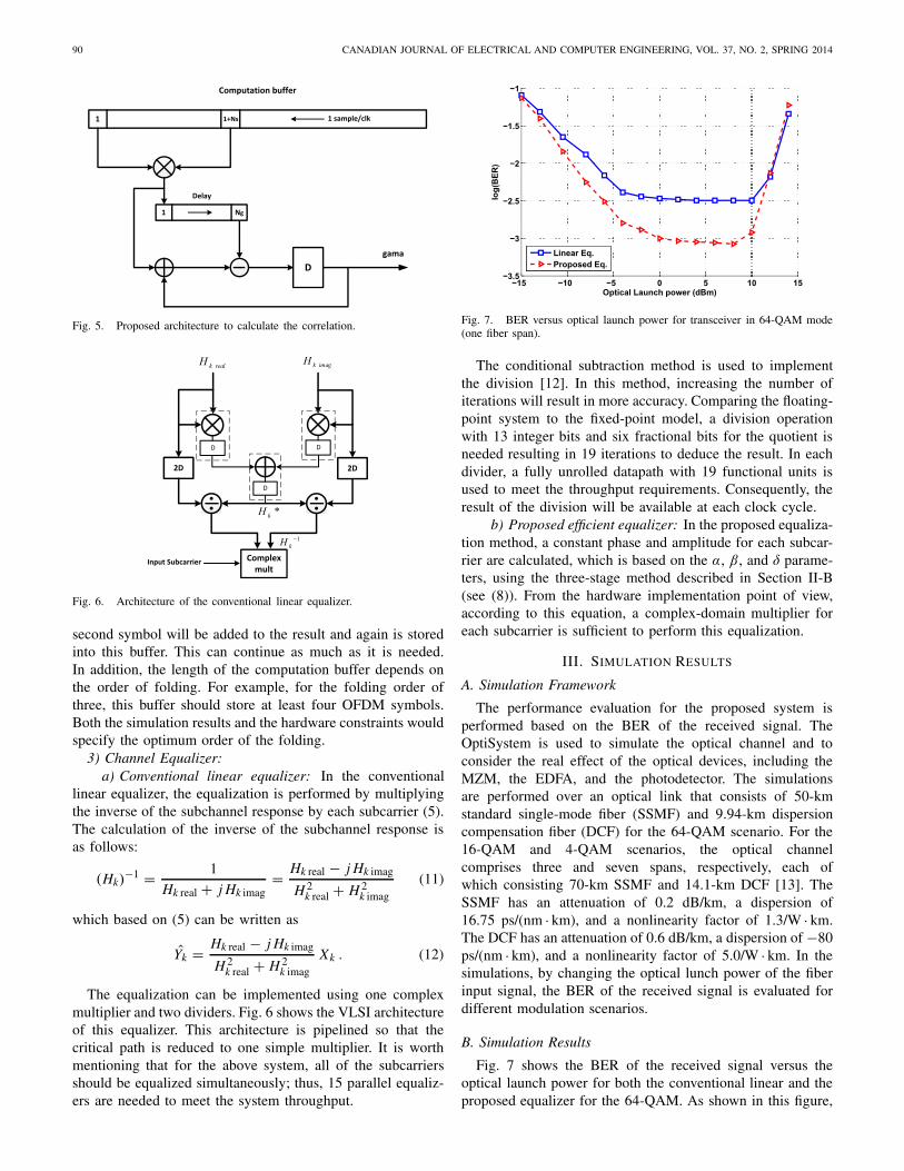
2) Symbol Synchronization: The synchronization blockshould perform the computations in (1) and (2). To calculatethe correlation, a buffer is used to store the received symbols.This buffer, called the computation buffer, is used to store atleast two consecutive symbols. In the buffer, samples of theOFDM signal are shifting with the rate of one sample per clockcycle. Therefore, instead of using 40 complex multipliers,only one multiplier and a delay buffer with the CP lengthare used (Fig. 5). After eight clock cycles, the first valueof γ is calculated and then, one new value for γ will beproduced in each clock cycle. Finally, a simple comparatorfinds the maximum value and detects the peak position. In theproposed architecture, the number of multiplication is reducedto one. In this architecture, reducing the number of functionalunits reduces the hardware complexity and also the systemthroughput, which undoubtedly may lead to some frame loss.This, however, is not an issue as this procedure is performedonly when the system is in the reset mode.
To implement the folding technique in the above architec-ture, a simple buffer with the length of the OFDM symbol isneeded to store γ values. After storing the first symbol, the
90 CANADIAN JOURNAL OF ELECTRICAL AND COMPUTER ENGINEERING, VOL. 37, NO. 2, SPRING 2014
Fig. 5. Proposed architecture to calculate the correlation.
Fig. 6. Architecture of the conventional linear equalizer.
second symbol will be added to the result and again is storedinto this buffer. This can continue as much as it is needed.In addition, the length of the computation buffer depends onthe order of folding. For example, for the folding order ofthree, this buffer should store at least four OFDM symbols.Both the simulation results and the hardware constraints wouldspecify the optimum order of the folding.
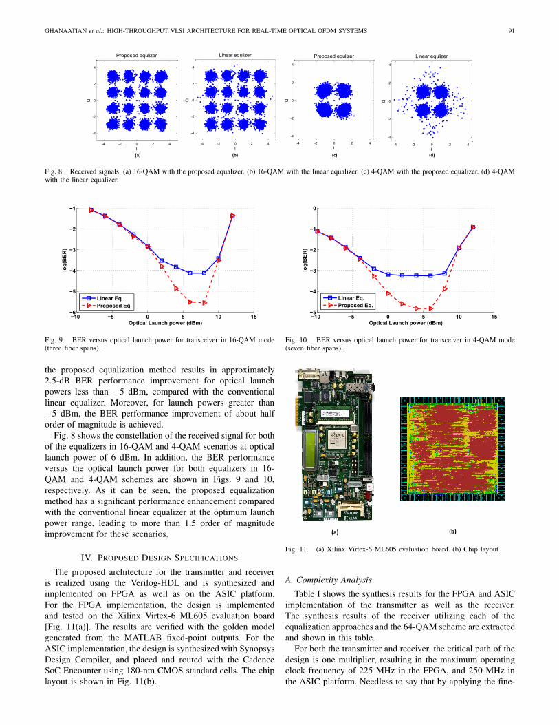
3) Channel Equalizer:a) Conventional linear equalizer: In the conventional
linear equalizer, the equalization is performed by multiplyingthe inverse of the subchannel response by each subcarrier (5).The calculation of the inverse of the subchannel response isas follows:
(Hk)−1 = 1
Hk real + j Hk imag= Hk real − j Hk imag
H 2k real + H 2
k imag
(11)
which based on (5) can be written as
Yk = Hk real − j Hk imag
H 2k real + H 2
k imag
Xk . (12)
The equalization can be implemented using one complexmultiplier and two dividers. Fig. 6 shows the VLSI architectureof this equalizer. This architecture is pipelined so that thecritical path is reduced to one simple multiplier. It is worthmentioning that for the above system, all of the subcarriersshould be equalized simultaneously; thus, 15 parallel equaliz-ers are needed to meet the system throughput.
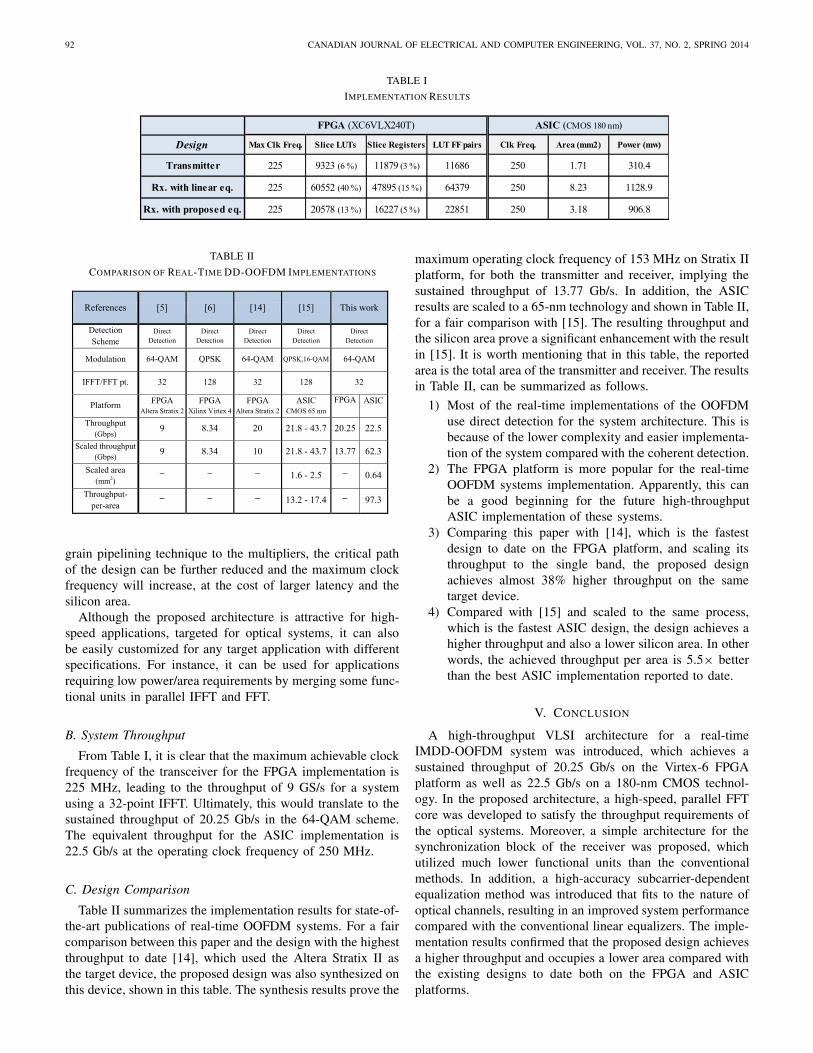
Fig. 7. BER versus optical launch power for transceiver in 64-QAM mode(one fiber span).
The conditional subtraction method is used to implementthe division [12]. In this method, increasing the number ofiterations will result in more accuracy. Comparing the floating-point system to the fixed-point model, a division operationwith 13 integer bits and six fractional bits for the quotient isneeded resulting in 19 iterations to deduce the result. In eachdivider, a fully unrolled datapath with 19 functional units isused to meet the throughput requirements. Consequently, theresult of the division will be available at each clock cycle.
b) Proposed efficient equalizer: In the proposed equaliza-tion method, a constant phase and amplitude for each subcar-rier are calculated, which is based on the α, β, and δ parame-ters, using the three-stage method described in Section II-B(see (8)). From the hardware implementation point of view,according to this equation, a complex-domain multiplier foreach subcarrier is sufficient to perform this equalization.
III. SIMULATION RESULTS
A. Simulation Framework
The performance evaluation for the proposed system isperformed based on the BER of the received signal. TheOptiSystem is used to simulate the optical channel and toconsider the real effect of the optical devices, including theMZM, the EDFA, and the photodetector. The simulationsare performed over an optical link that consists of 50-kmstandard single-mode fiber (SSMF) and 9.94-km dispersioncompensation fiber (DCF) for the 64-QAM scenario. For the16-QAM and 4-QAM scenarios, the optical channelcomprises three and seven spans, respectively, each ofwhich consisting 70-km SSMF and 14.1-km DCF [13]. TheSSMF has an attenuation of 0.2 dB/km, a dispersion of16.75 ps/(nm · km), and a nonlinearity factor of 1.3/W · km.The DCF has an attenuation of 0.6 dB/km, a dispersion of −80ps/(nm · km), and a nonlinearity factor of 5.0/W · km. In thesimulations, by changing the optical lunch power of the fiberinput signal, the BER of the received signal is evaluated fordifferent modulation scenarios.
B. Simulation Results
Fig. 7 shows the BER of the received signal versus theoptical launch power for both the conventional linear and theproposed equalizer for the 64-QAM. As shown in this figure,
GHANAATIAN et al.: HIGH-THROUGHPUT VLSI ARCHITECTURE FOR REAL-TIME OPTICAL OFDM SYSTEMS 91
Fig. 8. Received signals. (a) 16-QAM with the proposed equalizer. (b) 16-QAM with the linear equalizer. (c) 4-QAM with the proposed equalizer. (d) 4-QAMwith the linear equalizer.
Fig. 9. BER versus optical launch power for transceiver in 16-QAM mode(three fiber spans).
the proposed equalization method results in approximately2.5-dB BER performance improvement for optical launchpowers less than −5 dBm, compared with the conventionallinear equalizer. Moreover, for launch powers greater than−5 dBm, the BER performance improvement of about halforder of magnitude is achieved.
Fig. 8 shows the constellation of the received signal for bothof the equalizers in 16-QAM and 4-QAM scenarios at opticallaunch power of 6 dBm. In addition, the BER performanceversus the optical launch power for both equalizers in 16-QAM and 4-QAM schemes are shown in Figs. 9 and 10,respectively. As it can be seen, the proposed equalizationmethod has a significant performance enhancement comparedwith the conventional linear equalizer at the optimum launchpower range, leading to more than 1.5 order of magnitudeimprovement for these scenarios.
IV. PROPOSED DESIGN SPECIFICATIONS
The proposed architecture for the transmitter and receiveris realized using the Verilog-HDL and is synthesized andimplemented on FPGA as well as on the ASIC platform.For the FPGA implementation, the design is implementedand tested on the Xilinx Virtex-6 ML605 evaluation board[Fig. 11(a)]. The results are verified with the golden modelgenerated from the MATLAB fixed-point outputs. For theASIC implementation, the design is synthesized with SynopsysDesign Compiler, and placed and routed with the CadenceSoC Encounter using 180-nm CMOS standard cells. The chiplayout is shown in Fig. 11(b).
Fig. 10. BER versus optical launch power for transceiver in 4-QAM mode(seven fiber spans).
Fig. 11. (a) Xilinx Virtex-6 ML605 evaluation board. (b) Chip layout.
A. Complexity Analysis
Table I shows the synthesis results for the FPGA and ASICimplementation of the transmitter as well as the receiver.The synthesis results of the receiver utilizing each of theequalization approaches and the 64-QAM scheme are extractedand shown in this table.
For both the transmitter and receiver, the critical path of thedesign is one multiplier, resulting in the maximum operatingclock frequency of 225 MHz in the FPGA, and 250 MHz inthe ASIC platform. Needless to say that by applying the fine-
92 CANADIAN JOURNAL OF ELECTRICAL AND COMPUTER ENGINEERING, VOL. 37, NO. 2, SPRING 2014
TABLE I
IMPLEMENTATION RESULTS
TABLE II
COMPARISON OF REAL-TIME DD-OOFDM IMPLEMENTATIONS
grain pipelining technique to the multipliers, the critical pathof the design can be further reduced and the maximum clockfrequency will increase, at the cost of larger latency and thesilicon area.
Although the proposed architecture is attractive for high-speed applications, targeted for optical systems, it can alsobe easily customized for any target application with differentspecifications. For instance, it can be used for applicationsrequiring low power/area requirements by merging some func-tional units in parallel IFFT and FFT.
B. System Throughput
From Table I, it is clear that the maximum achievable clockfrequency of the transceiver for the FPGA implementation is225 MHz, leading to the throughput of 9 GS/s for a systemusing a 32-point IFFT. Ultimately, this would translate to thesustained throughput of 20.25 Gb/s in the 64-QAM scheme.The equivalent throughput for the ASIC implementation is22.5 Gb/s at the operating clock frequency of 250 MHz.
C. Design Comparison
Table II summarizes the implementation results for state-of-the-art publications of real-time OOFDM systems. For a faircomparison between this paper and the design with the highestthroughput to date [14], which used the Altera Stratix II asthe target device, the proposed design was also synthesized onthis device, shown in this table. The synthesis results prove the
maximum operating clock frequency of 153 MHz on Stratix IIplatform, for both the transmitter and receiver, implying thesustained throughput of 13.77 Gb/s. In addition, the ASICresults are scaled to a 65-nm technology and shown in Table II,for a fair comparison with [15]. The resulting throughput andthe silicon area prove a significant enhancement with the resultin [15]. It is worth mentioning that in this table, the reportedarea is the total area of the transmitter and receiver. The resultsin Table II, can be summarized as follows.
1) Most of the real-time implementations of the OOFDMuse direct detection for the system architecture. This isbecause of the lower complexity and easier implementa-tion of the system compared with the coherent detection.
2) The FPGA platform is more popular for the real-timeOOFDM systems implementation. Apparently, this canbe a good beginning for the future high-throughputASIC implementation of these systems.
3) Comparing this paper with [14], which is the fastestdesign to date on the FPGA platform, and scaling itsthroughput to the single band, the proposed designachieves almost 38% higher throughput on the sametarget device.
4) Compared with [15] and scaled to the same process,which is the fastest ASIC design, the design achieves ahigher throughput and also a lower silicon area. In otherwords, the achieved throughput per area is 5.5× betterthan the best ASIC implementation reported to date.
V. CONCLUSION
A high-throughput VLSI architecture for a real-timeIMDD-OOFDM system was introduced, which achieves asustained throughput of 20.25 Gb/s on the Virtex-6 FPGAplatform as well as 22.5 Gb/s on a 180-nm CMOS technol-ogy. In the proposed architecture, a high-speed, parallel FFTcore was developed to satisfy the throughput requirements ofthe optical systems. Moreover, a simple architecture for thesynchronization block of the receiver was proposed, whichutilized much lower functional units than the conventionalmethods. In addition, a high-accuracy subcarrier-dependentequalization method was introduced that fits to the nature ofoptical channels, resulting in an improved system performancecompared with the conventional linear equalizers. The imple-mentation results confirmed that the proposed design achievesa higher throughput and occupies a lower area compared withthe existing designs to date both on the FPGA and ASICplatforms.
GHANAATIAN et al.: HIGH-THROUGHPUT VLSI ARCHITECTURE FOR REAL-TIME OPTICAL OFDM SYSTEMS 93
ACKNOWLEDGMENT
The authors would like to thank Prof. Salehi andDr. Beyranvand for their helpful suggestion through this work.
REFERENCES
[1] S. Tian, K. Panta, H. A. Suraweera, B. J. C. Schmidt, S. McLaughlin,and J. Armstrong, “A novel timing synchronization method for ACO-OFDM-based optical wireless communications,” IEEE Trans. WirelessCommun., vol. 7, no. 12, pp. 4958–4967, Dec. 2008.
[2] J. Armstrong, “OFDM for optical communications,” J. Ligthw. Technol.,vol. 27, no. 3, pp. 189–204, Feb. 1, 2009.
[3] Y. Tang, “High-speed optical transmission system using coherent opticalorthogonal frequency-division multiplexing,” Ph.D. dissertation,Dept. Electr. Electron. Eng., Univ. Melbourne, Melbourne, Australia,2010.
[4] W. Shieh, “OFDM for flexible high-speed optical networks,” J. Lightw.Technol., vol. 29, no. 10, pp. 1560–1577, May 15, 2011.
[5] E. Hugues-Salas et al., “Directly modulated VCSEL-based real-time11.25-Gb/s optical OFDM transmission over 2000-m legacy MMFs,”IEEE Photon. J., vol. 4, no. 1, pp. 143–154, Feb. 2012.
[6] Y. Benlachtar et al., “Real-time digital signal processing for the gen-eration of optical orthogonal frequency-division-multiplexed signals,”IEEE J. Sel. Topics Quantum Electron., vol. 16, no. 5, pp. 1235–1244,Sep./Oct. 2010.
[7] R. I. Killey et al., “Recent progress on real-time DSP for direct detectionoptical OFDM transceivers,” in Proc. Conf. OFC/NFOEC, 2011.
[8] M. H. Shoreh, H. Beyranvand, and J. A. Salehi, “Mathematical modelingof nonlinearity impairments in optical OFDM communication systemsusing multiple optical phase conjugate,” in Proc. IWCIT, May 2013,pp. 1–5.
[9] S. Coleri, M. Ergen, A. Puri, and A. Bahai, “Channel estimationtechniques based on pilot arrangement in OFDM systems,” IEEE Trans.Broadcast., vol. 48, no. 3, pp. 223–229, Sep. 2002.
[10] B. J. C. Schmidt, A. J. Lowery, and J. Armstrong, “Experimentaldemonstrations of electronic dispersion compensation for long-haultransmission using direct-detection optical OFDM,” J. Lightw. Technol.,vol. 26, no. 1, pp. 196–203, Jan. 1, 2008.
[11] R. Chassaing and D. Reay, Digital Signal Processing and ApplicationsWith the TMS320C6713 and TMS320C6416 DSK, 2nd ed. Hoboken, NJ,USA: Wiley, 2008.
[12] N. Kehtarnavaz, Real-Time Digital Signal Processing Based on theTMS320C6000. New York, NY, USA: Elsevier, 2004.
[13] E. Ip and J. M. Kahn, “Compensation of dispersion and nonlinearimpairments using digital backpropagation,” J. Lightw. Technol., vol. 26,no. 20, pp. 3416–3425, Oct. 15, 2008.
[14] E. Hugues-Salas, R. P. Giddings, and J. M. Tang, “First experimentaldemonstration of real-time adaptive transmission of 20 Gb/s dual-bandoptical OFDM signals over 500 m OM2 MMFs,” in Proc. OFC/NFOEC,2013, pp. 1–3.
[15] R. Bouziane et al., “Design studies for ASIC implementations of 28 GS/soptical QPSK- and 16-QAM OFDM transceivers,” Opt. Exp., vol. 9,no. 21, pp. 20857–20864, 2011.
Reza Ghanaatian was born in Jahrom, Iran, on May13, 1988. He received the B.Sc. degree in electricalengineering from the Khaje Nasir University ofTechnology (KNTU), Tehran, Iran, in 2010, and theM.Sc. degree in digital systems from the Departmentof Electrical Engineering, Sharif University of Tech-nology (SUT), Tehran, in 2012.
He has been with Advanced Integrated CircuitDesign Laboratory (AICDL), Sharif University ofTechnology since 2010. His current research inter-ests include VLSI architecture design of digital
signal processing algorithms for wireless and optical communication systemsand field-programmable gate array-based systems.
Mahdi Shabany received the B.Sc. degree in electri-cal engineering from the Sharif University of Tech-nology (SUT), Tehran, Iran, in 2002, and the M.Sc.and Ph.D. degrees in electrical engineering from theUniversity of Toronto, Toronto, ON, Canada, in 2004and 2008, respectively.
He is an Associate Professor with the Electri-cal Engineering Department, Sharif University ofTechnology and also works with the University ofToronto periodically as a Visiting Researcher. Hewas with Redline Communications Co., Toronto,
from 2007 to 2008, where he developed and patented designs for WiMAX sys-tems. He also served as a Postdoctoral Fellow with the University of Toronto in2009. He holds three U.S. patents. His current research interests include digitalelectronics, VLSI architecture/algorithm design for broadband communicationsystems, efficient implementation of signal processing algorithms for variousapplications including imaging, and bio-oriented systems.
Morteza H. Shoreh was born in Tehran, Iran, onJanuary 9, 1988. He received the B.Sc. degree inelectrical engineering from the University of Tehran(UT), in 2010, and the M.Sc. degree in communica-tion system from the Department of Electrical Engi-neering, Sharif University of Technology (SUT),Tehran, in 2012.
He has been with Optical Networks ResearchLab (ONRL), since 2011, under the supervision ofProf. Jawad A. Salehi. His current research inter-ests include high-speed optical communications, all-
optical networking devices, nonlinear optics, optical signal processing, opticalnetworks (CO-OFDM and OFDM-CDMA), and wireless communicationssystems and networks.
Recommended