En vue de l'obtention du
DOCTORAT DE L'UNIVERSITÉ DE TOULOUSEDélivré par :
Institut National Polytechnique de Toulouse (INP Toulouse)Discipline ou spécialité :
Micro Nano Systèmes
Présentée et soutenue par :Mme LAVINIA-ELENA CIOTIRCA
le mardi 23 mai 2017
Titre :
Unité de recherche :
Ecole doctorale :
System design of a low-power three-axis underdamped MEMSaccelerometer with simultaneous electrostatic damping control
Génie Electrique, Electronique, Télécommunications (GEET)
Laboratoire d'Analyse et d'Architecture des Systèmes (L.A.A.S.)Directeur(s) de Thèse :
MME HELENE TAP
Rapporteurs :M. JEROME JUILLARD, SUPELEC
M. PASCAL NOUET, UNIVERSITE MONTPELLIER 2
Membre(s) du jury :M. PHILIPPE BENECH, INP DE GRENOBLE, Président
Mme HELENE TAP, INP TOULOUSE, MembreM. OLIVIER BERNAL, INP TOULOUSE, Membre


Acknowledgement
The research work presented in this thesis was carried out between 2014 and 2017 at the
Laboratory for Analysis and Architecture of Systems (LAAS) in Toulouse with collaboration of
the Sensors Solutions Design (SSD) Team at NXP Semiconductors (previously Freescale
Semiconductors).
Firstly, I would like to express my sincere gratitude to Prof. Hélène Tap and Mr. Philippe
Lance for offering me the opportunity to carry out this research and for supervising this project. I
would like to thank Hélène for her continuous support and guidance and for always being positive
towards my work. Her motivation and patience helped me in all the time of research and writing
of this thesis. I would also like to thank Philippe for his constant support and for the worthy advice
on both research as well as on my career development.
Further, I would also like to thank the rest of my thesis committee Prof. Pascal Nouet, Prof.
Jérôme Juillard and Prof. Philippe Benech for taking the time to review this thesis and for their
insightful comments.
This thesis would not have been possible without the close guidance of Dr. Olivier Bernal,
Mr. Jérôme Enjalbert and Mr. Thierry Cassagnes. I would like to express my gratitude for all their
help, technical expertise and constant encouragement. I will always appreciate and remember their
patience and kindness.
I am grateful to Dr. Robert Dean and Dr. Chong Li for offering me the opportunity to
develop this research work within their facilities during my stay at Auburn University, USA.
I would also like to thank Ms. Peggy Kniffin, Mr. Aaron Geisberger and Mr. Bob Steimle
for the MEMS modeling guidance and Mr. Clément Tronche, Mr. Francis Jayat and Mr. Philippe
Calmettes for providing their help with the experimental set up and my samples demands.
Likewise, I want to hereby acknowledge the contributions of my colleagues at NXP
Semiconductors as well as all the OSE (LAAS) group members. In particular, my sincere thanks
go to all the doctoral students I had the chance to meet during this research work, for all their help
and day to day support: Antonio Luna Arriaga, Evelio Ramirez Miquet, Jalal Al Roumy, Laura Le
Barbier, Mohanad Albughdadi, Raül da Costa Moreira, Lucas Perbet, Blaise Mulliez, Yu Zhao,
Fernando Urgiles, Harris Apriyanto and Mengkoung Veng.
I have no words to express my gratitude to all the friends I had or have made during these
last three years. Their permanent encouragement, motivation, attention and care helped me to
successfully complete this work. I would like to thank all of them for the special moments we have
shared together and for never letting me down. Infinite thanks!
Last but not the least, I would like to present my deepest gratitude to my parents, Mia and
Mircea, who have always encouraged and supported me to follow my dreams! I would like to
thank them, and my little brother, Liviu, for the unconditioned love, trust, kindness and for being
a constant source of inspiration. To them I dedicate this thesis!

Abstract
Recently, consumer electronics industry has known a spectacular growth that would have
not been possible without pushing the integration barrier further and further. Micro Electro
Mechanical Systems (MEMS) inertial sensors (e.g. accelerometers, gyroscopes) provide high
performance, low power, low die cost solutions and are, nowadays, embedded in most consumer
applications.
In addition, the sensors fusion has become a new trend and combo sensors are gaining
growing popularity since the co-integration of a three-axis MEMS accelerometer and a three-axis
MEMS gyroscope provides complete navigation information. The resulting device is an Inertial
measurement unit (IMU) able to sense multiple Degrees of Freedom (DoF).
Nevertheless, the performances of the accelerometers and the gyroscopes are conditioned
by the MEMS cavity pressure: the accelerometer is usually a damped system functioning under an
atmospheric pressure while the gyroscope is a highly resonant system. Thus, to conceive a combo
sensor, a unique low cavity pressure is required. The integration of both transducers within the
same low pressure cavity necessitates a method to control and reduce the ringing phenomena by
increasing the damping factor of the MEMS accelerometer. Consequently, the aim of the thesis is
the design of an analog front-end interface able to sense and control an underdamped three-axis
MEMS accelerometer.
This work proposes a novel closed-loop accelerometer interface achieving low power
consumption. The design challenge consists in finding a trade-off between the sampling frequency,
the settling time and the circuit complexity since the sensor excitation plates are multiplexed
between the measurement and the damping phases. In this context, a patented damping sequence
(simultaneous damping) has been conceived to improve the damping efficiency over the state of
the art approach performances (successive damping).
To investigate the feasibility of the novel electrostatic damping control architecture, several
mathematical models have been developed and the settling time method is used to assess the
damping efficiency. Moreover, a new method that uses the multirate signal processing theory and
allows the system stability study has been developed. This very method is used to conclude on the
loop stability for a certain sampling frequency and loop gain value.
Next, a CMOS implementation of the entire accelerometer signal chain is designed. The
functioning has been validated and the block may be further integrated within an ASIC. Finally,
a discrete components system is designed to experimentally validate the simultaneous damping
approach.

Résumé
L’intégration de plusieurs capteurs inertiels au sein d’un même dispositif de type MEMS
afin de pouvoir estimer plusieurs degrés de liberté devient un enjeu important pour le marché de
l’électronique grand public à cause de l’augmentation et de la popularité croissante des
applications embarquées.
Aujourd’hui, les efforts d'intégration se concentrent autour de la réduction de la taille, du
coût et de la puissance consommée. Dans ce contexte, la co-intégration d’un accéléromètre trois-
axes avec un gyromètre trois-axes est cohérente avec la quête conjointe de ces trois objectifs.
Toutefois, cette co-intégration doit s’opérer dans une même cavité basse pression afin de préserver
un facteur de qualité élevé nécessaire au bon fonctionnement du gyromètre. Dans cette optique, un
nouveau système de contrôle, qui utilise le principe de l’amortissement électrostatique, a été conçu
pour permettre l’utilisation d’un accéléromètre sous-amorti naturellement. Le principe utilisé pour
contrôler l’accéléromètre est d’appliquer dans la contre-réaction une force électrostatique générée
à partir de l’estimation de la vitesse du MEMS. Cette technique permet d’augmenter le facteur
d’amortissement et de diminuer le temps d’établissement de l’accéléromètre.
L’architecture proposée met en œuvre une méthode novatrice pour détecter et contrôler le
mouvement d’un accéléromètre capacitif en technologie MEMS selon trois degrés de liberté : x, y
et z. L'accélération externe appliquée au capteur peut être lue en utilisant la variation de capacité
qui apparaît lorsque la masse se déplace. Lors de la phase de mesure, quand une tension est
appliquée sur les électrodes du MEMS, une variation de charge est appliquée à l’entrée de
l’amplificateur de charge (Charge-to-Voltage : C2V). La particularité de cette architecture est que
le C2V est partagé entre les trois axes, ce qui permet une réduction de surface et de puissance
consommée. Cependant, étant donné que le circuit ainsi que l’électrode mobile (commune aux
trois axes du MEMS) sont partagés, on ne peut mesurer qu’un seul axe à la fois.
Ainsi, pendant la phase d'amortissement, une tension de commande, calculée pendant les
phases de mesure précédentes, est appliquée sur les électrodes d'excitation du MEMS. Cette
tension de commande représente la différence entre deux échantillons successifs de la tension de
sortie du C2V et elle est mémorisée et appliquée trois fois sur les électrodes d’excitation pendant
la même période d’échantillonnage.
Afin d’étudier la faisabilité de cette technique, des modèles mathématiques, Matlab-
Simulink et VerilogA ont été développés. Le principe de fonctionnement basé sur l’amortissement
électrostatique simultané a été validé grâce à ces modèles. Deux approches consécutives ont été
considérées pour valider expérimentalement cette nouvelle technique : dans un premier temps
l’implémentation du circuit en éléments discrets associé à un accéléromètre sous vide est
présentée. En perspective, un accéléromètre sera intégré dans la même cavité qu’un gyromètre, les
capteurs étant instrumentés à l’aide de circuits CMOS intégrés. Dans cette cadre, la conception en
technologie CMOS 0.18µm de l’interface analogique d’amortissement est présentée et validée par
simulation dans le manuscrit.


i
CONTENTS
Contents ..................................................................................................................................................... i
List of Figures ......................................................................................................................................... v
List of Tables .......................................................................................................................................... ix
List of Abbreviations ........................................................................................................................... xi
Introduction ........................................................................................................................................... 1
A. Background and motivation ................................................................................ 1
B. Research direction and contributions .................................................................. 1
C. Thesis organization ............................................................................................. 2
1. Inertial sensors............................................................................................................................... 5
1.1 Introduction .............................................................................................................. 5
1.2 Degrees of freedom and types of motion in inertial sensors ................................... 5
1.3 Consumer market MEMS inertial sensors ............................................................... 6
1.4 Discrete inertial sensors ............................................................................................ 8
1.4.1 Accelerometers ...........................................................................................................9
A. Piezoresistive acceleration sensing .....................................................................9
B. Piezoelectric acceleration sensing .....................................................................10
C. Capacitive acceleration sensing ........................................................................10
D. Other acceleration sensing methods ..................................................................12
1.4.2 Gyroscopes ................................................................................................................13
1.5 Combo Sensors ....................................................................................................... 14
1.6 Summary ................................................................................................................. 16
2. CMOS MEMS Accelerometers ........................................................................................... 17
2.1 Mechanical capacitive sensing element and second order mass spring damper
model ..................................................................................................................... 17
2.2 Physics of the capacitive sensing element ........................................................................ 19
CONTENTS
ii
2.3 Electrostatic actuation ........................................................................................... 21
2.3.1 Electrostatic Actuation mechanism ..........................................................................21
2.3.2 Static Pull-in voltage .................................................................................................22
2.3.3 Spring Softening Effect.............................................................................................23
2.4 CMOS Capacitive Accelerometers Interfaces ....................................................... 24
2.4.1 Open-loop capacitive architectures for MEMS accelerometers ..............................25
2.4.2 Closed-loop capacitive architectures for MEMS accelerometers .............................27
2.5 Summary ................................................................................................................. 30
3. Three-axis high-Q MEMS accelerometer with electrostatic damping
control – modelling ................................................................................................................... 33
3.1 Introduction ........................................................................................................... 33
3.2 Three-axis Sensor Element .................................................................................... 34
3.2.1 Sensor Design ..........................................................................................................34
3.2.2 Matlab-Simulink model and s-domain transfer function ..........................................36
3.2.3 z-domain MEMS transfer function ...........................................................................39
3.3 Analog interface: Charge-to-voltage amplifier modeling ..................................... 41
3.4 Voltage to force conversion .................................................................................. 43
3.4.1 Electrostatic damping linearity principle .................................................................43
3.4.2 Linearity of the voltage-to-force conversion ...........................................................45
3.4.3 Bias calculation for electrostatic force optimization ...............................................47
3.5 Discrete Controller: Derivative Block .................................................................... 49
3.5.1 Derivative block – principle of operation ................................................................49
3.5.2 Derivative block - modeling ....................................................................................51
3.6 Damping approaches ............................................................................................. 52
3.4.1 Successive damping .................................................................................................53
3.4.2 Simultaneous damping .............................................................................................56
3.4.3 Performances and choice of architecture .................................................................57
3.7 Multirate controller modeling in z-domain ........................................................... 59
3.8 Closed-loop transfer function and stability study .................................................. 61
CONTENTS
iii
3.9 Summary ............................................................................................................... 64
4. Towards a CMOS interface for a three-axis high Q MEMS
accelerometer with simultaneous damping control ........................................... 65
4.1 System design of a low-power three-axis underdamped MEMS accelerometer with
simultaneous electrostatic damping control .......................................................... 65
4.2 MEMS Accelerometer Verilog A – Spectre Model .............................................. 66
4.3 Charge to voltage converter (C2V) ....................................................................... 69
4.3.1 Block diagram and clock diagram ...........................................................................69
4.3.2 Basics of CMOS Analog Design and C2V Architecture choice .............................71
4.3.3 Design and performances ........................................................................................74
4.4 Switched capacitor derivative block ...................................................................... 77
4.5 Derivative gain amplifier ....................................................................................... 82
4.6 CMOS Switches ..................................................................................................... 88
4.7 Excitation signals block .......................................................................................... 90
4.8 Closed-loop system validation ............................................................................... 91
4.9 Summary ................................................................................................................. 92
Conclusions and perspectives................................................................................ 95
Bibliography ........................................................................................................... 97
Appendices ............................................................................................................ 109

CONTENTS
iv
v
List of Figures
Figure 1.1 A representation of the possible movements of an object in a three-dimensional space
[Snyder, 2016] .................................................................................................................................6
Figure 1.2 MEMS revenue forecast 2015-2021 per application [Yole, 2016] ...............................6
Figure 1.3 (a) Accelerometer applications vs. performances [Domingues, 2013] ..........................7
Figure 1.3 (b) Gyroscope applications vs. performances [Domingues, 2013] ..............................7
Figure 1.4 An illustration of a piezoresistive accelerometer ..........................................................9
Figure 1.5 An illustration of a piezoelectric accelerometer ..........................................................10
Figure 1.6 An illustration of a capacitive accelerometer with interdigitated fingers ..................11
Figure 1.7 Typical structure of in-plane (left) and out-of-plane (right) capacitive MEMS
accelerometer [Renaut, 2013] ........................................................................................................12
Figure 1.8 Functioning principle of in-plane (left) and out-of-plane capacitive MEMS
accelerometer [Renaut, 2013] ........................................................................................................12
Figure 1. 9 A representation of the Coriolis gyroscope model .....................................................13
Figure 1.10 Inertial sensors revenue forecast 2012-2019 [Yole, 2014] .........................................14
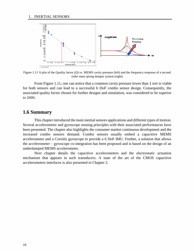
Figure 1.11 A plot of the Quality factor (Q) vs. MEMS cavity pressure (left) and the frequency
response of a second order mass spring damper system (right).....................................................15
Figure 2.1 An illustration of a second order mass spring damper system .....................................17
Figure 2.2 An illustration of the capacitive sensing principle ......................................................19
Figure 2.3 Capacitance variation dependency on MEMS displacement and the linear region of
operation (highlighted in red) ........................................................................................................20
Figure 2.4 An illustration of a single electrode motion structure .................................................22
Figure 2.5. An illustration of a three-plate capacitive structure ...................................................24
Figure 2.6 Conceptual block diagram of a closed-loop MEMS accelerometer ............................25
Figure 2.7 Block diagram of the open-loop digital Σ∆ interface [Amini, 2004] ..........................26
Figure 2.8 Block diagram of an nth order Σ∆ digital closed-loop accelerometer .........................28
Figure 2.9 Block diagram of an analogue closed-loop accelerometer ..........................................30
Figure 3.1. Three-axis closed-loop underdamped MEMS accelerometer with electrostatic
damping control ............................................................................................................................34
LIST OF FIGURES
vi
Figure 3.2. An illustration of the dual-mass three-axis differential accelerometer with self-test
capabilities and the analog frond end block diagram ....................................................................35
Figure 3.3 An illustration of the Simulink model for the open loop MEMS accelerometer .........37
Figure 3.4. MEMS accelerometer response in open loop configuration to a 1g step acceleration
for different quality factors: (a) Q=1, (b) Q=50 and (c) Q=2000 ..................................................38
Figure 3.5 Step response of the open loop accelerometer for Q=5 ................................................39
Figure 3.6 Bode plot of the continuous-time MEMS transfer function (blue) and the associated
discrete-time Euler approximated TF (red) for fs=30kHz and Q=2000 ........................................40
Figure 3.7 Bode plot of the continuous-time MEMS transfer function (blue) and the associated
discrete-time Tustin approximated TF (red) for fs=30kHz and Q=2000 .......................................41
Figure 3.8 Block diagram of the capacitive sensing element and the AFE’s first stage with its
chronograms ..................................................................................................................................42
Figure 3.9 An illustration of the MEMS and the C2V simplified models .....................................42
Figure 3.10 An illustration of a parallel plate capacitive sensor and the electrostatic forces
applied on the proof mass ..............................................................................................................43
Figure 3.11 Net electrostatic force simulation when the input acceleration varies from -8g to 8g
and the control voltage Vctrl varies from -0.4V to 0.4V ..............................................................46
Figure 3.12 Net electrostatic force nonlinearity when the input acceleration varies from -8g to 8g
and the control voltage Vctrl varies from -0.4V to 0.4V ..............................................................46
Figure 3.13 Excitation signals simulations using the optimal values found for VB and Vctrl......48
Figure 3.14 Net electrostatic forces simulation when VB varies from 0V to 0.8V ......................49
Figure 3.15 System block diagram ................................................................................................50
Figure 3.16 Derivative simulation for several sampling rates (a) Ts=2µs (b) Ts=5µs and (c)
Ts=10µs (discrete derivative – green and continuous-time derivative red waveform) .................50
Figure 3.17 Block diagram of the derivative model where S&H refers to sample and hold ........51
Figure 3.18 Simulation results of the derivative block .................................................................52
Figure 3.19 Classical approach: successive damping chronograms .............................................53
Figure 3.20 (a) Block diagram model of the successive damping system ....................................54
Figure 3.20 (b) Sensor model used in Figure 3.20 (a) to output the charge variation due to the
acceleration variation ....................................................................................................................54
Figure 3.20 (c) Derivative model used in Figure 3.20 (a) to output the control voltage V_ctrlx ..55
Figure 3.21 Clock chronograms used to control the closed loop system implementing successive
damping .........................................................................................................................................55
Figure 3.22 Novel sequence: simultaneous damping chronograms ..............................................56
LIST OF FIGURES
vii
Figure 3.23 Clock chronograms used to control the closed loop system implementing
simultaneous damping ..................................................................................................................57
Figure 3.24 Electrostatic force waveforms for both approaches: successive and simultaneous
damping .........................................................................................................................................58
Figure 3.25 Settling time simulation results for both approaches: successive and simultaneous
damping .........................................................................................................................................58
Figure 3.26 Simplified block diagram of the discretized system ................................................59
Figure 3.27 Simplified discrete model using up-sampling and down-sampling blocks ...............60
Figure 3.28 Simplified Discrete model for the multirate controller .............................................61
Figure 3.29 Equivalent open loop system .....................................................................................63
Figure 3.30. (kd, Ts) stable points ................................................................................................63
Figure 4.1. Block diagram of the accelerometer signal chain for x-axis .......................................66
Figure 4.2. An illustration of the MEMS accelerometer Cadence symbol ...................................67
Figure 4.3 Open-loop MEMS displacement for Q=2 and Q=2000 ...............................................68
Figure 4.4 Open-loop plates configuration for electrostatic force test .........................................68
Figure 4.5 (a) Block diagram of the AFE’s first stage (C2V) .......................................................70
Figure 4.5 (b) Chronograms of the C2V block and x-axis excitation signals................................70
Figure 4.6 (a) Telescopic-cascode amplifier and (b) folded-cascode amplifier [Johns – Martin,
1997] ..............................................................................................................................................71
Figure 4.7 (a) Folded-cascode amplifier with PMOS differential input pair (b) simplified folded-
cascode amplifier to calculate the voltage gain [Razavi, 2001] .....................................................72
Figure 4.8 (a) Basic current mirror (b) cascode current mirror [Razavi, 2001] .............................73
Figure 4.9 Folded-cascode OTA with second stage and Miller compensation .............................75
Figure 4.10 Two stages Folded-cascode amplifier – biases generation ........................................76
Figure 4.11 Amplifier Module and Phase – stability analysis ......................................................77
Figure 4.12 (a) and (b) An illustration of the derivative block .....................................................78
Figure 4.13 Chronograms of the derivative block .........................................................................79
Figure 4.14 Chronograms of the derivative block ........................................................................79
Figure 4.15 Derivative block simulation and illustration of the derivative block outputs during
the reading phase ...........................................................................................................................81
Figure 4.16 Derivative block simulation and illustration of the derivative outputs out of the
reading phases ...............................................................................................................................81
Figure 4.17 A representation of the switched-capacitors derivative gain block ..........................82
Figure 4.18 A representation of the single stage fully-differential amplifier ...............................83
LIST OF FIGURES
viii
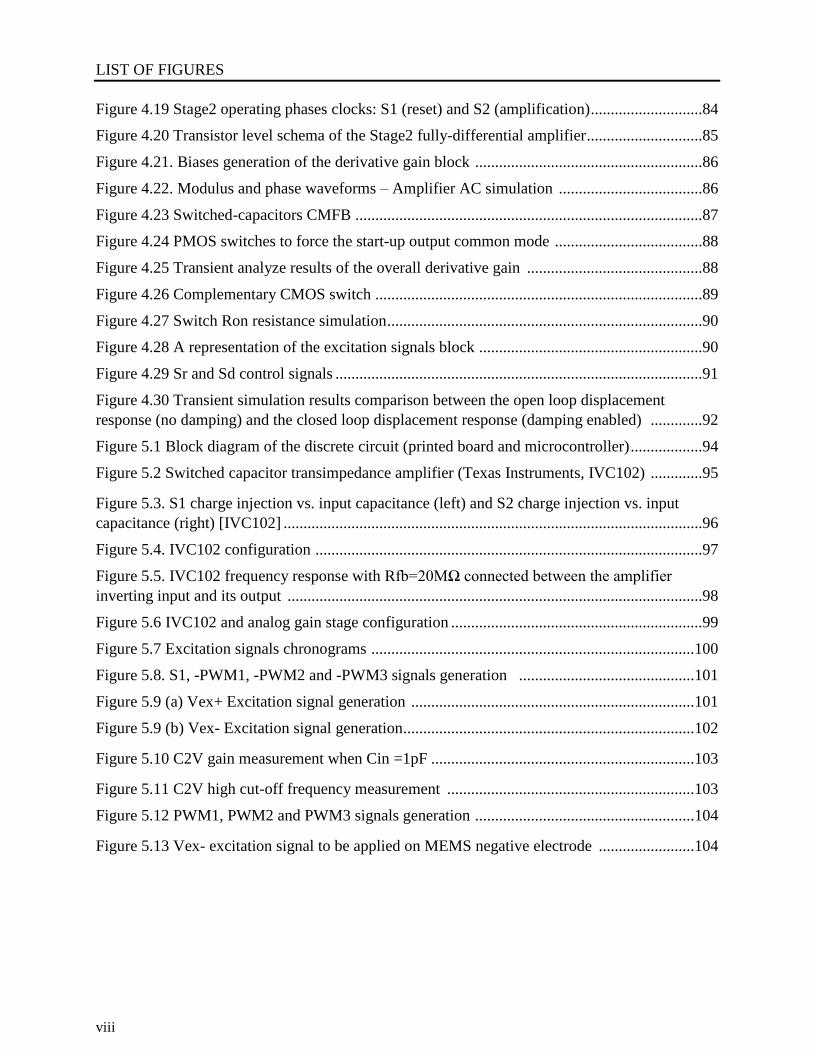
Figure 4.19 Stage2 operating phases clocks: S1 (reset) and S2 (amplification) ............................84
Figure 4.20 Transistor level schema of the Stage2 fully-differential amplifier .............................85
Figure 4.21. Biases generation of the derivative gain block .........................................................86
Figure 4.22. Modulus and phase waveforms – Amplifier AC simulation ....................................86
Figure 4.23 Switched-capacitors CMFB .......................................................................................87
Figure 4.24 PMOS switches to force the start-up output common mode .....................................88
Figure 4.25 Transient analyze results of the overall derivative gain ............................................88
Figure 4.26 Complementary CMOS switch ..................................................................................89
Figure 4.27 Switch Ron resistance simulation ...............................................................................90
Figure 4.28 A representation of the excitation signals block ........................................................90
Figure 4.29 Sr and Sd control signals ............................................................................................91
Figure 4.30 Transient simulation results comparison between the open loop displacement
response (no damping) and the closed loop displacement response (damping enabled) .............92
Figure 5.1 Block diagram of the discrete circuit (printed board and microcontroller) ..................94
Figure 5.2 Switched capacitor transimpedance amplifier (Texas Instruments, IVC102) .............95
Figure 5.3. S1 charge injection vs. input capacitance (left) and S2 charge injection vs. input
capacitance (right) [IVC102] .........................................................................................................96
Figure 5.4. IVC102 configuration .................................................................................................97
Figure 5.5. IVC102 frequency response with Rfb=20MΩ connected between the amplifier
inverting input and its output ........................................................................................................98
Figure 5.6 IVC102 and analog gain stage configuration ...............................................................99
Figure 5.7 Excitation signals chronograms .................................................................................100
Figure 5.8. S1, -PWM1, -PWM2 and -PWM3 signals generation ............................................101
Figure 5.9 (a) Vex+ Excitation signal generation .......................................................................101
Figure 5.9 (b) Vex- Excitation signal generation.........................................................................102
Figure 5.10 C2V gain measurement when Cin =1pF ..................................................................103
Figure 5.11 C2V high cut-off frequency measurement ..............................................................103
Figure 5.12 PWM1, PWM2 and PWM3 signals generation .......................................................104
Figure 5.13 Vex- excitation signal to be applied on MEMS negative electrode ........................104
ix
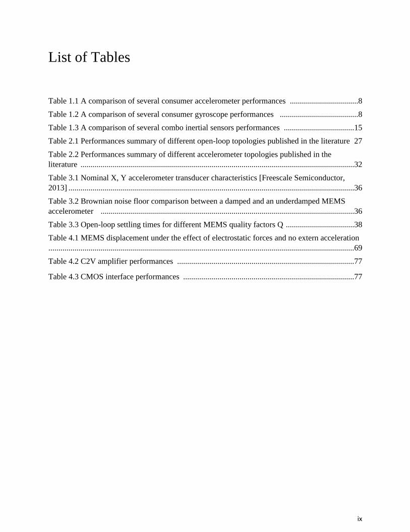
List of Tables
Table 1.1 A comparison of several consumer accelerometer performances ..................................8
Table 1.2 A comparison of several consumer gyroscope performances .......................................8
Table 1.3 A comparison of several combo inertial sensors performances ...................................15
Table 2.1 Performances summary of different open-loop topologies published in the literature 27
Table 2.2 Performances summary of different accelerometer topologies published in the
literature ........................................................................................................................................32
Table 3.1 Nominal X, Y accelerometer transducer characteristics [Freescale Semiconductor,
2013] ..............................................................................................................................................36
Table 3.2 Brownian noise floor comparison between a damped and an underdamped MEMS
accelerometer ..............................................................................................................................36
Table 3.3 Open-loop settling times for different MEMS quality factors Q ..................................38
Table 4.1 MEMS displacement under the effect of electrostatic forces and no extern acceleration
........................................................................................................................................................69
Table 4.2 C2V amplifier performances ........................................................................................77
Table 4.3 CMOS interface performances .....................................................................................77

LIST OF TABLES
x
xi
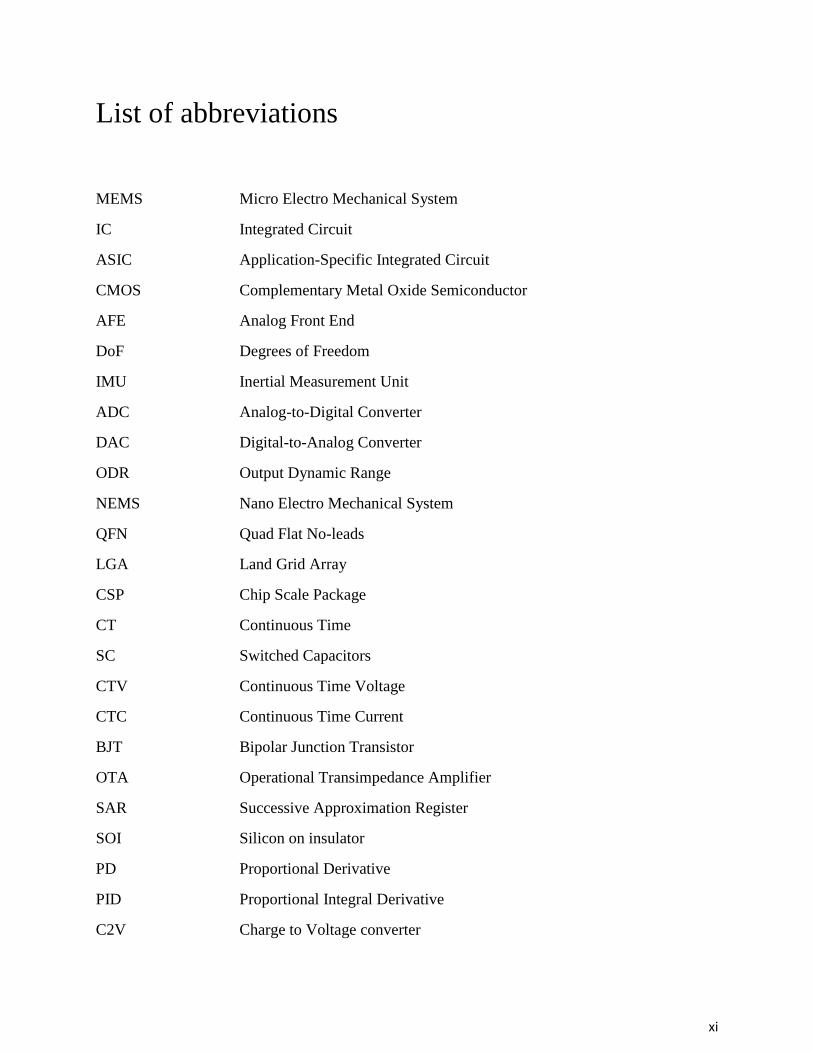
List of abbreviations
MEMS Micro Electro Mechanical System
IC Integrated Circuit
ASIC Application-Specific Integrated Circuit
CMOS Complementary Metal Oxide Semiconductor
AFE Analog Front End
DoF Degrees of Freedom
IMU Inertial Measurement Unit
ADC Analog-to-Digital Converter
DAC Digital-to-Analog Converter
ODR Output Dynamic Range
NEMS Nano Electro Mechanical System
QFN Quad Flat No-leads
LGA Land Grid Array
CSP Chip Scale Package
CT Continuous Time
SC Switched Capacitors
CTV Continuous Time Voltage
CTC Continuous Time Current
BJT Bipolar Junction Transistor
OTA Operational Transimpedance Amplifier
SAR Successive Approximation Register
SOI Silicon on insulator
PD Proportional Derivative
PID Proportional Integral Derivative
C2V Charge to Voltage converter

LIST OF ABBREVIATIONS
xii
CDS Correlated Double Sampling
SNR Signal to Noise Ration
BW Bandwidth
GBW Gain Bandwidth product
MPZ Matched Pole-Zero
MMPZ Modified Matched Pole-Zero
CMFB Control Mode Feedback
TI Texas Instruments
PWM Pulse Width Modulation
1
INTRODUCTION
A. Background and motivation
Over the past years, cutting-edge advances in electronics and in microfabrication have
allowed the integration of multiple sensors within integrated analog and digital circuits to design
Micro Electro Mechanical Systems (MEMS). MEMS are widely used in industries that include
but are not limited to: medicine, automotive, aeronautic, aerospace and consumer electronics
[Yole, 2016].
Nowadays, the devices are becoming smarter due to microelectronics progresses but also
taking more and more advantage of integrated sensors. Among them, inertial sensors (e.g.
accelerometers, gyroscopes) have known an important development and are employed in shock
detection, healthcare (walking stability monitoring in Parkinson’s disease patients), seismology,
image and video stabilization, drop protection or motion control applications [Domingues, 2013].
Extensive consumer market growth, in terms of inertial sensors, has been possible due to
continuous power, cost and surface reduction while maintaining high performances. Moreover, a
trend that enables both cost and surface reduction, and came out recently, is the sensors fusion.
An accelerometer senses the linear motion of the device itself while the gyroscope
measures the angular rotation, along one, two or three directions, often named Degrees of Freedom
(DoF). To determine the dynamic behavior of a device, a three-axis accelerometer and a three-axis
gyroscope can be fused to provide complete navigational information. The result is an inertial
measurement unit (IMU) able to sense multiple DoF.
Freescale Semiconductor Inc. (acquired by NXP Semiconductors in December 2015) was
one of the first semiconductors companies in the world and leader in automotive electronics,
microcontrollers and microprocessors solutions. Further, NXP Semiconductors (45000 employees
in 2016 and $6.1 billion revenue in 2015) provides strong expertise in security, near-field
communication systems (NFC), sensors, radio frequency and power management systems.
Consumer electronics have also gained its place in NXP Semiconductors portfolio, which includes
accelerometers, gyroscopes, magnetometers, temperature and pressure sensors products. However,
no accelerometer-gyroscope combo sensor is yet available in their portfolio.
In this context, the research carried out in this thesis, funded by NXP Semiconductors
together with ANRT (Association Nationale Recherche Technologie), has as main objective the
design of a combo six DoF sensor, compatible with a single MEMS cavity technology.
B. Research direction and contributions
Inertial sensors, embedded in consumer electronics, are usually capacitive accelerometers
and Coriolis vibratory gyroscopes. Their principle of operation and performances are conditioned
INTRODUCTION
2
by the MEMS cavity pressure: the accelerometer is a damped system functioning under an
atmospheric pressure while the gyroscope is a highly resonant system. To conceive a combo
sensor, a unique low cavity pressure is required. The integration of both transducers within the
same low pressure cavity necessitates a method to control and reduce the ringing phenomena by
increasing the damping factor of the MEMS accelerometer. Hence, the goal of the thesis is the
system design of an underdamped capacitive MEMS accelerometer.
The most used accelerometer control configurations are the digital closed loop (Σ∆
architecture) and the analog loop, enabling artificial damping by superimposing two electrostatic
forces on the accelerometer proof mass to produce a linear feedback characteristic [Boser, 1996].
The former approach has a complex implementation and is not compatible with the actual
transducer design (since the proof-mass is shared between the three-axis) while the latter provides
good performances and can be used to control multiple DoF.
Firstly, this thesis proposes a novel closed-loop electrostatic damping architecture for a
three-axis underdamped accelerometer. The circuit is a switched-capacitor low-power system that
multiplexes the analog front-end (AFE) first stage between the three axes, to reduce both power
and surface. Additionally, a new damping sequence (simultaneous damping), has been conceived
to improve the damping efficiency over the state of the art approach performances (successive
damping). The simultaneous damping sequence is implemented using a multirate control method.
Next, to validate the system operation, several behavioral and mathematical models have
been designed and the settling time method is used to assess the damping efficiency.
In addition, a new approach that uses the multirate signal processing theory and allows the
system stability study has been developed. This method is used to conclude on the loop stability
for a certain sampling frequency and loop gain value.
Using the above techniques, a CMOS implementation of the entire accelerometer signal
chain is designed. The functioning has been validated and the block may be further integrated
within an ASIC. Finally, a discrete components system is designed to experimentally validate the
simultaneous damping approach.
C. Thesis organization
This thesis is organized as follows. Chapter 1 introduces the main inertial sensors
applications, focusing on accelerometer and gyroscopes sensing principles and performances. This
first chapter also highlights the consumer electronics continuous development and the increased
combo sensors demand. In this context, this thesis research direction and main objective have been
set.
Chapter 2 presents the fundamentals of the capacitive MEMS accelerometers including the
physics of the mechanical sensing element, the second order mass spring damper model and the
electrostatic actuation mechanism. A synopsis of the existing accelerometer CMOS interfaces is
also briefly presented.
In Chapter 3, a new closed-loop accelerometer architecture that overcomes the
underdamped MEMS oscillation issue is presented. The sensor control relies on the electrostatic
damping principle and consists in estimating the proof mass velocity and in artificially increasing

INTRODUCTION
3
the damping ratio. The Matlab-Simulink model for each block in the loop is described and the
simulation results are shown. Then, a comparison between the novel simultaneous damping
approach performances and the classical successive damping method is made. Finally, the
multirate controller modeling and the system closed loop stability are analyzed.
Chapter 4 introduces a block by block transistor level design of the proposed damping
architecture, adapted for a three-axis low power MEMS accelerometer. The switched capacitor
technique is used to implement the read-out interface and the multirate controller block. The closed
loop simulation results and performances are shown.
Finally, the thesis classically ends with a conclusion that summarizes the results and
contributions, and suggests several future research directions and perspectives.

INTRODUCTION
4
5
CHAPTER 1
INERTIAL SENSORS
1.1 Introduction
A sensor is a device that detects and converts any physical quantity (e.g. light, heat,
pressure, motion, inertia, etc.) into a signal which can be electronically measured and further
processed. Nowadays, sensors are widely used in applications that include but are not limited to:
medicine, automotive, aeronautic and aerospace industries, but also in consumer electronics.
While the first sensor dates from the nineteenth century (a thermocouple), during the First
and the Second World War, sensors as infrared, motion and inertial sensors, intended for strategical
and tactical applications, have known an important development and improvement.
An inertial sensor is an observer who is caught within a completely shielded case and who
is trying to determine the position changes of the case with respect to an outer inertial reference
system [Kempe, 2011]. In other words, inertial sensors deal with the inertial forces to find the
dynamic behavior of an object; these inertial forces modify the dynamic behavior and cause
accelerations and angular velocities along one or several directions. Accordingly, the main inertial
sensors are the accelerometer, which senses a linear motion and the gyroscope which measures the
angular rotation.
Since the beginning of the 1990’s, the inertial sensors are predominantly Micro Electro
Mechanical Systems (MEMS) due to their low cost, high performances and high level of
integration. Their advantages opened new markets and developed new applications, each one with
its own specifications and constraints. The classical accelerometers and gyroscopes applications
are: shock detection (airbag – automotive industry), seismology, aeronautics and space industry,
healthcare (patient activity monitoring, disease identification), image and video stabilization,
wearable computing, drop protection or motion control.
1.2 Degrees of freedom and types of motion in inertial sensors
The accelerations and the angular velocities, measured by an accelerometer or by a
gyroscope, are vectors having an absolute value and an orientation. If only one vector component
is measured, then the system is said to be a one-axis or one-DoF. If two vector components
(acceleration or angular velocity) are measured, the system is a two-degree of freedom and so on.
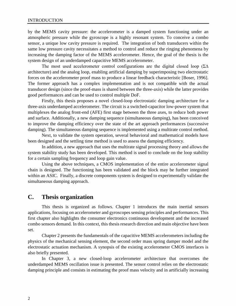
It is thus clear that in a three-dimensional space, one can measure six degrees of freedom as shown
in Figure 1.1. Three of DoF are translational movements: surge, heave and sway (often noted x, y
and z) and can be measured using an accelerometer. The other three DoF represent rotational
movements (yaw, pitch and roll) and can be sensed using a gyroscope sensor. Thus, the
combination of the translational and rotational movements consists in a six DoF system requiring
both a three-axis accelerometer and a three-axis gyroscope to determine its dynamic
1. INERTIAL SENSORS
6
behavior. Therefore, an inertial measurement unit (IMU) should embed a multiaxis accelerometer
and a multiaxis gyroscope to provide all the required navigation information; the combination of
an accelerometer and a gyroscope is often also called a combo sensor.
Figure 1.1 A representation of the possible movements of an object in a three-dimensional space [Snyder, 2016]
1.3 Consumer market MEMS inertial sensors
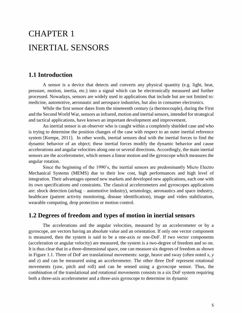
The consumer electronics industry is one of the markets that has continually grown over
the past few years and this is mainly due to the technological progress and to consumer requests.
Along with the overall market growth, consumer MEMS sensors also known an important
development to enable cost, surface and power reductions while maintaining high performances.
Figure 1.2 presents a MEMS revenue forecast which firstly, confirms the increasing revenue for
the upcoming years and secondly, presents the consumer MEMS dominancy over the other sensor
sectors as Aeronautics, Automotive, Defense, Industrial, Medical and Telecom.
Figure 1.2 MEMS revenue forecast 2015-2021 per application [Yole, 2016]
1. INERTIAL SENSORS
7
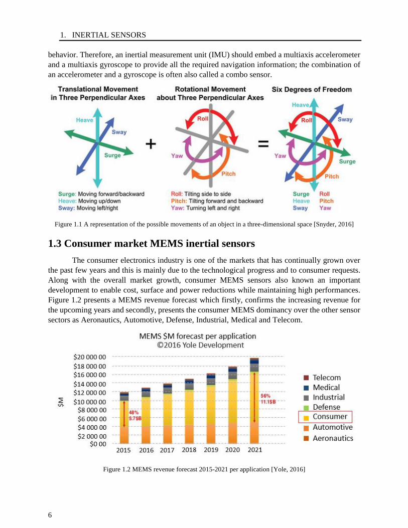
Inertial MEMS sensors, the accelerometer as well as the gyroscope, are widely used in
consumer market applications (smartphones, tablets, cameras, smart home devices, wearables,
remote control, gaming, etc.). However, there is an important gap between the performances of an
inertial sensor intended for consumer electronics and an automotive, medical or defense inertial
sensor. Figure 1.3 (a) and (b) [Domingues, 2013] presents a sensor performances comparison for
different applications.
For example, a consumer market accelerometer has an input range which can go up to 8𝑔
and requires a dynamic range between 60 𝑑𝐵 and 100 𝑑𝐵 while a seismology accelerometer, for
the same input range, needs a much higher accuracy and a dynamic range between 140 𝑑𝐵 and
160 𝑑𝐵.
Figure 1.3 (a) Accelerometer applications vs. performances [Domingues, 2013]
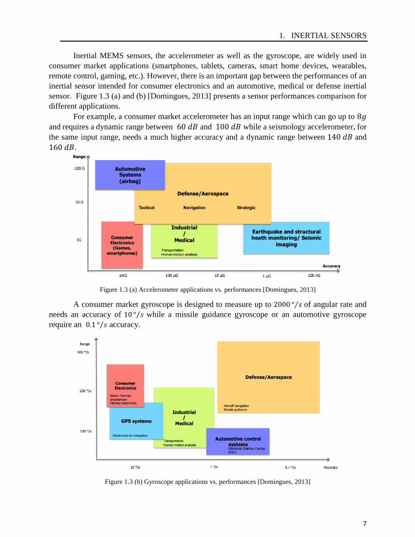
A consumer market gyroscope is designed to measure up to 2000 ° 𝑠⁄ of angular rate and
needs an accuracy of 10 ° 𝑠⁄ while a missile guidance gyroscope or an automotive gyroscope
require an 0.1 ° 𝑠⁄ accuracy.
Figure 1.3 (b) Gyroscope applications vs. performances [Domingues, 2013]
1. INERTIAL SENSORS
8
On the other hand, the main constraints of a consumer market inertial sensor are the cost,
the size and the power consumption. As it was shown, the industry targeting this market imposes
high volume production thus the cost is very important. Silicon area and power consumption
should also be considered to enable inertial sensors to be integrated within everyday user
applications.
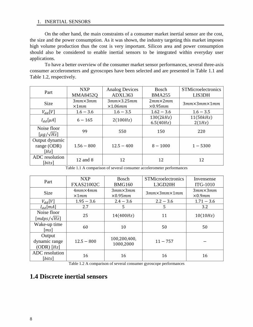
To have a better overview of the consumer market sensor performances, several three-axis
consumer accelerometers and gyroscopes have been selected and are presented in Table 1.1 and
Table 1.2, respectively.
Part NXP
MMA8452Q
Analog Devices
ADXL363
Bosch
BMA255
STMicroelectronics
LIS3DH
Size 3𝑚𝑚×3𝑚𝑚×1𝑚𝑚
3𝑚𝑚×3.25𝑚𝑚×1.06𝑚𝑚
2𝑚𝑚×2𝑚𝑚×0.95𝑚𝑚
3𝑚𝑚×3𝑚𝑚×1𝑚𝑚
𝑉𝑑𝑑[𝑉] 1.6 − 3.6 1.6 − 3.5 1.62 − 3.6 1.6 − 3.5
𝐼𝑑𝑑[𝜇𝐴] 6 − 165 2(100𝐻𝑧) 130(2𝑘𝐻𝑧) 6.5(40𝐻𝑧)
11(50𝑘𝐻𝑧) 2(1𝐻𝑧)
Noise floor
[𝜇𝑔 √𝐻𝑧⁄ ] 99 550 150 220
Output dynamic
range (ODR) [𝐻𝑧]
1.56 − 800 12.5 − 400 8 − 1000 1 − 5300
ADC resolution [𝑏𝑖𝑡𝑠]
12 and 8 12 12 12
Table 1.1 A comparison of several consumer accelerometer performances
Part NXP
FXAS21002C
Bosch
BMG160
STMicroelectronics
L3GD20H
Invensense
ITG-1010
Size 4𝑚𝑚×4𝑚𝑚×1𝑚𝑚
3𝑚𝑚×3𝑚𝑚×0.95𝑚𝑚
3𝑚𝑚×3𝑚𝑚×1𝑚𝑚 3𝑚𝑚×3𝑚𝑚×0.9𝑚𝑚
𝑉𝑑𝑑[𝑉] 1.95 − 3.6 2.4 − 3.6 2.2 − 3.6 1.71 − 3.6 𝐼𝑑𝑑[𝑚𝐴] 2.7 5 5 3.2
Noise floor
[𝑚𝑑𝑝𝑠 √𝐻𝑧⁄ ] 25 14(400𝐻𝑧) 11 10(10𝐻𝑧)
Wake-up time [𝑚𝑠]
60 10 50 50
Output
dynamic range
(ODR) [𝐻𝑧]
12.5 − 800 100,200,400,
1000,2000 11 − 757 −
ADC resolution [𝑏𝑖𝑡𝑠]
16 16 16 16
Table 1.2 A comparison of several consumer gyroscope performances
1.4 Discrete inertial sensors
1. INERTIAL SENSORS
9
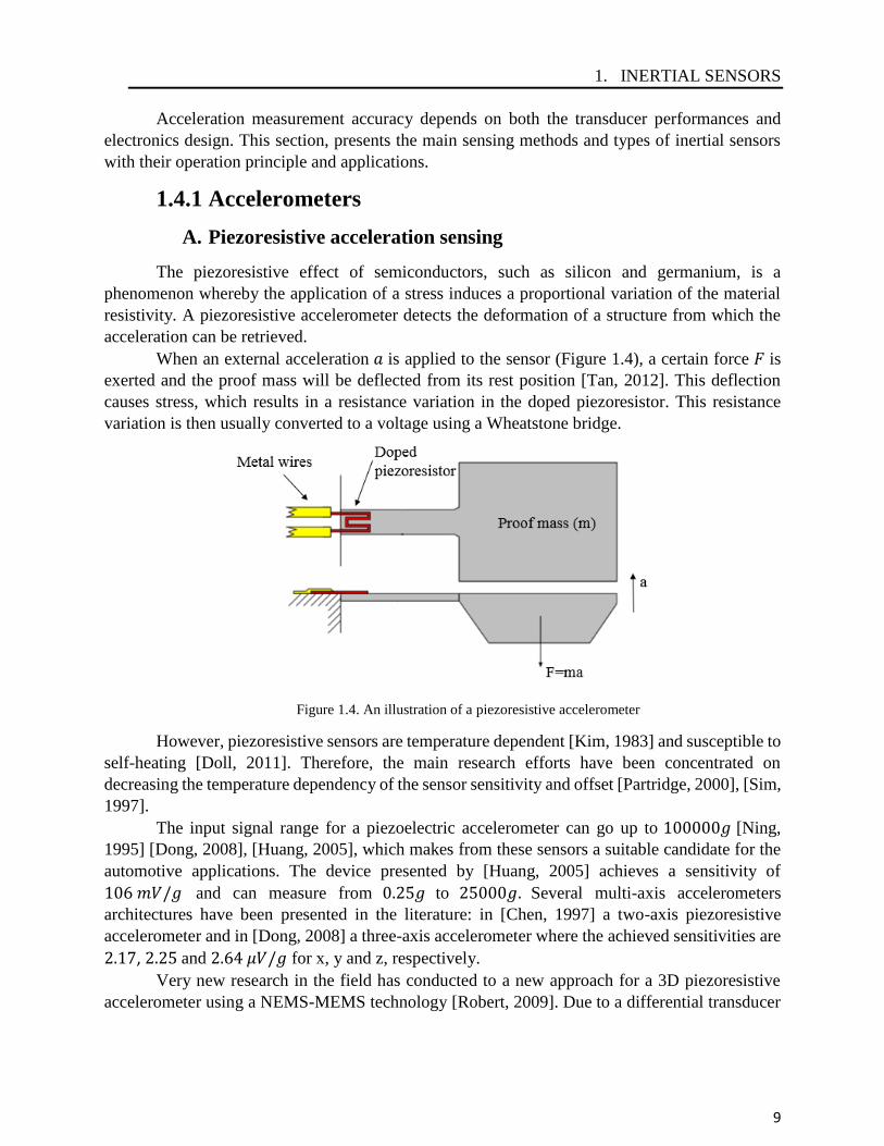
Acceleration measurement accuracy depends on both the transducer performances and
electronics design. This section, presents the main sensing methods and types of inertial sensors
with their operation principle and applications.
1.4.1 Accelerometers
A. Piezoresistive acceleration sensing
The piezoresistive effect of semiconductors, such as silicon and germanium, is a
phenomenon whereby the application of a stress induces a proportional variation of the material
resistivity. A piezoresistive accelerometer detects the deformation of a structure from which the
acceleration can be retrieved.
When an external acceleration 𝑎 is applied to the sensor (Figure 1.4), a certain force 𝐹 is
exerted and the proof mass will be deflected from its rest position [Tan, 2012]. This deflection
causes stress, which results in a resistance variation in the doped piezoresistor. This resistance
variation is then usually converted to a voltage using a Wheatstone bridge.
Figure 1.4. An illustration of a piezoresistive accelerometer
However, piezoresistive sensors are temperature dependent [Kim, 1983] and susceptible to
self-heating [Doll, 2011]. Therefore, the main research efforts have been concentrated on
decreasing the temperature dependency of the sensor sensitivity and offset [Partridge, 2000], [Sim,
1997].
The input signal range for a piezoelectric accelerometer can go up to 100000𝑔 [Ning,
1995] [Dong, 2008], [Huang, 2005], which makes from these sensors a suitable candidate for the
automotive applications. The device presented by [Huang, 2005] achieves a sensitivity of
106 𝑚𝑉/𝑔 and can measure from 0.25𝑔 to 25000𝑔. Several multi-axis accelerometers
architectures have been presented in the literature: in [Chen, 1997] a two-axis piezoresistive
accelerometer and in [Dong, 2008] a three-axis accelerometer where the achieved sensitivities are
2.17, 2.25 and 2.64 𝜇𝑉/𝑔 for x, y and z, respectively.
Very new research in the field has conducted to a new approach for a 3D piezoresistive
accelerometer using a NEMS-MEMS technology [Robert, 2009]. Due to a differential transducer
1. INERTIAL SENSORS
10
topology, the thermal sensitivity is reduced, but still, additional circuitry is required to compensate
the thermal drift, which remains the most important drawback of the piezoresistive accelerometer.
Piezoresistive accelerometers have typically noise floors between 10 and 100 𝜇𝑔/√𝐻𝑧 for
a bandwidth that ranges between 1 kHz and 10 kHz [Chatterjee, 2016].
B. Piezoelectric acceleration sensing
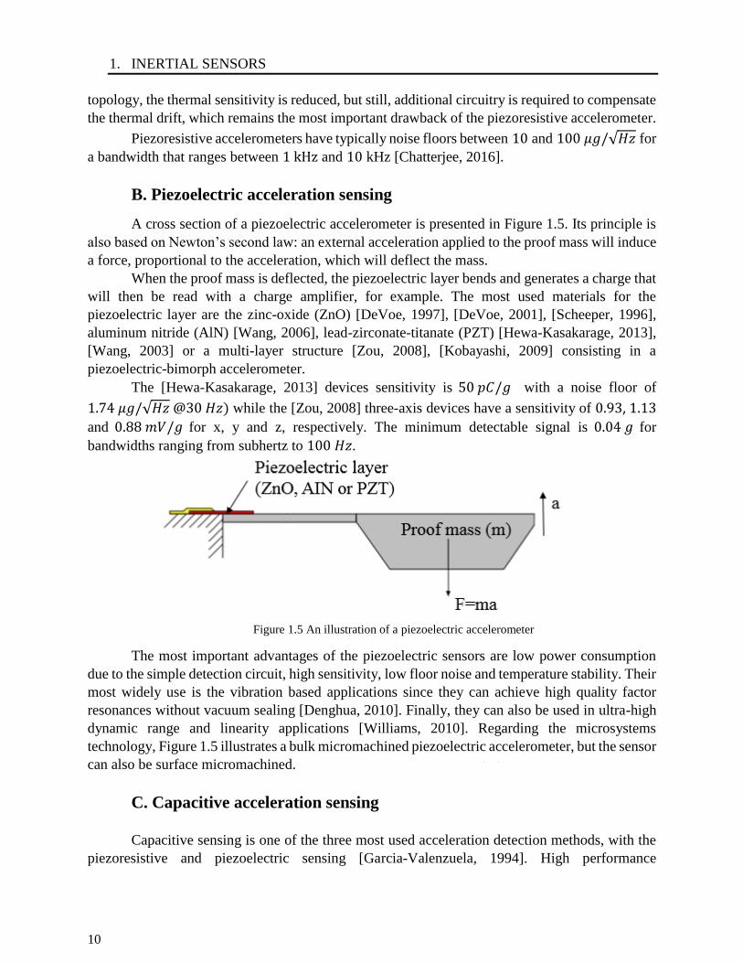
A cross section of a piezoelectric accelerometer is presented in Figure 1.5. Its principle is
also based on Newton’s second law: an external acceleration applied to the proof mass will induce
a force, proportional to the acceleration, which will deflect the mass. When the proof mass is deflected, the piezoelectric layer bends and generates a charge that
will then be read with a charge amplifier, for example. The most used materials for the
piezoelectric layer are the zinc-oxide (ZnO) [DeVoe, 1997], [DeVoe, 2001], [Scheeper, 1996],
aluminum nitride (AlN) [Wang, 2006], lead-zirconate-titanate (PZT) [Hewa-Kasakarage, 2013],
[Wang, 2003] or a multi-layer structure [Zou, 2008], [Kobayashi, 2009] consisting in a
piezoelectric-bimorph accelerometer.
The [Hewa-Kasakarage, 2013] devices sensitivity is 50 𝑝𝐶/𝑔 with a noise floor of
1.74 𝜇𝑔/√𝐻𝑧 @30 𝐻𝑧) while the [Zou, 2008] three-axis devices have a sensitivity of 0.93, 1.13
and 0.88 𝑚𝑉/𝑔 for x, y and z, respectively. The minimum detectable signal is 0.04 𝑔 for
bandwidths ranging from subhertz to 100 𝐻𝑧.
Figure 1.5 An illustration of a piezoelectric accelerometer
The most important advantages of the piezoelectric sensors are low power consumption
due to the simple detection circuit, high sensitivity, low floor noise and temperature stability. Their
most widely use is the vibration based applications since they can achieve high quality factor
resonances without vacuum sealing [Denghua, 2010]. Finally, they can also be used in ultra-high
dynamic range and linearity applications [Williams, 2010]. Regarding the microsystems
technology, Figure 1.5 illustrates a bulk micromachined piezoelectric accelerometer, but the sensor
can also be surface micromachined.
C. Capacitive acceleration sensing
Capacitive sensing is one of the three most used acceleration detection methods, with the
piezoresistive and piezoelectric sensing [Garcia-Valenzuela, 1994]. High performance
1. INERTIAL SENSORS
11
accelerometers are using a capacitive detection method since their fabrication cost is lower [Wu,
2002], they consume less power, they can be used in high sensitivity applications and are thermally
stable.
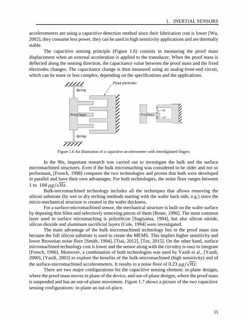
The capacitive sensing principle (Figure 1.6) consists in measuring the proof mass
displacement when an external acceleration is applied to the transducer. When the proof mass is
deflected along the sensing direction, the capacitance value between the proof mass and the fixed
electrodes changes. The capacitance change is then measured using an analog-front-end circuit,
which can be more or less complex, depending on the specifications and the applications.
Figure 1.6 An illustration of a capacitive accelerometer with interdigitated fingers
In the 90s, important research was carried out to investigate the bulk and the surface
micromachined structures. Even if the bulk micromaching was considered to be older and not so
performant, [French, 1998] compares the two technologies and proves that both were developed
in parallel and have their own advantages. For both technologies, the noise floor ranges between
1 to 100 𝜇𝑔/√𝐻𝑧 . Bulk-micromachined technology includes all the techniques that allows removing the
silicon substrate (by wet or dry etching methods starting with the wafer back side, e.g.) since the
micro-mechanical structure is created in the wafer thickness.
For a surface-micromachined sensor, the mechanical structure is built on the wafer surface
by deposing thin films and selectively removing pieces of them [Boser, 1996]. The most common
layer used in surface micromaching is polysilicon [Sugiyama, 1994], but also silicon nitride,
silicon dioxide and aluminum sacrificial layers [Cole, 1994] were investigated.
The main advantage of the bulk micromachined technology lies in the proof mass size
because the full silicon substrate is used to create the MEMS. This implies higher sensitivity and
lower Brownian noise floor [Smith, 1994], [Tsai, 2012], [Tez, 2015]. On the other hand, surface
micromachined technology cost is lower and the sensor along with the circuitry is easy to integrate
[French, 1996]. Moreover, a combination of both technologies was used by Yazdi et al., [Yazdi,
2000], [Yazdi, 2003] to explore the benefits of the bulk-micromachined (high sensitivity) and of
the surface-micromachined accelerometers. It results in a noise floor of 0.23 𝜇𝑔/√𝐻𝑧. There are two major configurations for the capacitive sensing element: in-plane designs,
where the proof mass moves in plane of the device, and out-of-plane designs, where the proof mass
is suspended and has an out-of-plane movement. Figure 1.7 shows a picture of the two capacitive
sensing configurations: in-plane an out-of-place.
1. INERTIAL SENSORS
12
Figure 1.7 Typical structure of in-plane (left) and out-of-plane (right) capacitive MEMS accelerometer [Renaut,
2013]
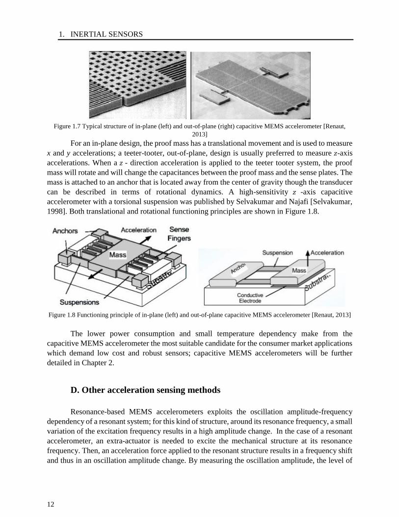
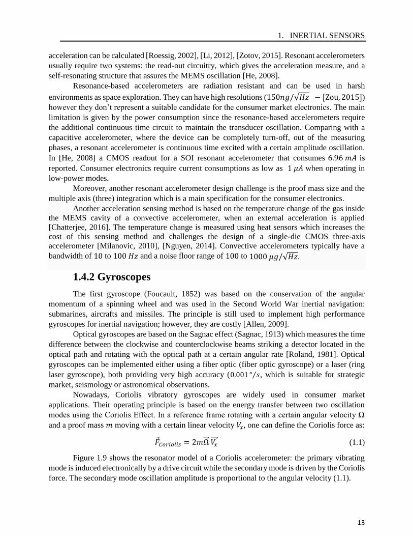
For an in-plane design, the proof mass has a translational movement and is used to measure
x and y accelerations; a teeter-tooter, out-of-plane, design is usually preferred to measure 𝑧-axis
accelerations. When a 𝑧 - direction acceleration is applied to the teeter tooter system, the proof
mass will rotate and will change the capacitances between the proof mass and the sense plates. The
mass is attached to an anchor that is located away from the center of gravity though the transducer
can be described in terms of rotational dynamics. A high-sensitivity 𝑧 -axis capacitive
accelerometer with a torsional suspension was published by Selvakumar and Najafi [Selvakumar,
1998]. Both translational and rotational functioning principles are shown in Figure 1.8.
Figure 1.8 Functioning principle of in-plane (left) and out-of-plane capacitive MEMS accelerometer [Renaut, 2013]
The lower power consumption and small temperature dependency make from the
capacitive MEMS accelerometer the most suitable candidate for the consumer market applications
which demand low cost and robust sensors; capacitive MEMS accelerometers will be further
detailed in Chapter 2.
D. Other acceleration sensing methods
Resonance-based MEMS accelerometers exploits the oscillation amplitude-frequency
dependency of a resonant system; for this kind of structure, around its resonance frequency, a small
variation of the excitation frequency results in a high amplitude change. In the case of a resonant
accelerometer, an extra-actuator is needed to excite the mechanical structure at its resonance
frequency. Then, an acceleration force applied to the resonant structure results in a frequency shift
and thus in an oscillation amplitude change. By measuring the oscillation amplitude, the level of
1. INERTIAL SENSORS
13
acceleration can be calculated [Roessig, 2002], [Li, 2012], [Zotov, 2015]. Resonant accelerometers
usually require two systems: the read-out circuitry, which gives the acceleration measure, and a
self-resonating structure that assures the MEMS oscillation [He, 2008].
Resonance-based accelerometers are radiation resistant and can be used in harsh
environments as space exploration. They can have high resolutions (150𝑛𝑔/√𝐻𝑧 − [Zou, 2015]) however they don’t represent a suitable candidate for the consumer market electronics. The main
limitation is given by the power consumption since the resonance-based accelerometers require
the additional continuous time circuit to maintain the transducer oscillation. Comparing with a
capacitive accelerometer, where the device can be completely turn-off, out of the measuring
phases, a resonant accelerometer is continuous time excited with a certain amplitude oscillation.
In [He, 2008] a CMOS readout for a SOI resonant accelerometer that consumes 6.96 𝑚𝐴 is
reported. Consumer electronics require current consumptions as low as 1 𝜇𝐴 when operating in
low-power modes.
Moreover, another resonant accelerometer design challenge is the proof mass size and the
multiple axis (three) integration which is a main specification for the consumer electronics.
Another acceleration sensing method is based on the temperature change of the gas inside
the MEMS cavity of a convective accelerometer, when an external acceleration is applied
[Chatterjee, 2016]. The temperature change is measured using heat sensors which increases the
cost of this sensing method and challenges the design of a single-die CMOS three-axis
accelerometer [Milanovic, 2010], [Nguyen, 2014]. Convective accelerometers typically have a
bandwidth of 10 to 100 𝐻𝑧 and a noise floor range of 100 to 1000 𝜇𝑔/√𝐻𝑧.
1.4.2 Gyroscopes
The first gyroscope (Foucault, 1852) was based on the conservation of the angular
momentum of a spinning wheel and was used in the Second World War inertial navigation:
submarines, aircrafts and missiles. The principle is still used to implement high performance
gyroscopes for inertial navigation; however, they are costly [Allen, 2009].
Optical gyroscopes are based on the Sagnac effect (Sagnac, 1913) which measures the time
difference between the clockwise and counterclockwise beams striking a detector located in the
optical path and rotating with the optical path at a certain angular rate [Roland, 1981]. Optical
gyroscopes can be implemented either using a fiber optic (fiber optic gyroscope) or a laser (ring
laser gyroscope), both providing very high accuracy (0.001 ° 𝑠⁄ , which is suitable for strategic
market, seismology or astronomical observations.
Nowadays, Coriolis vibratory gyroscopes are widely used in consumer market
applications. Their operating principle is based on the energy transfer between two oscillation
modes using the Coriolis Effect. In a reference frame rotating with a certain angular velocity Ω
and a proof mass 𝑚 moving with a certain linear velocity 𝑉𝑥, one can define the Coriolis force as:
𝐶𝑜𝑟𝑖𝑜𝑙𝑖𝑠 = 2𝑚Ω 𝑉𝑥 (1.1)
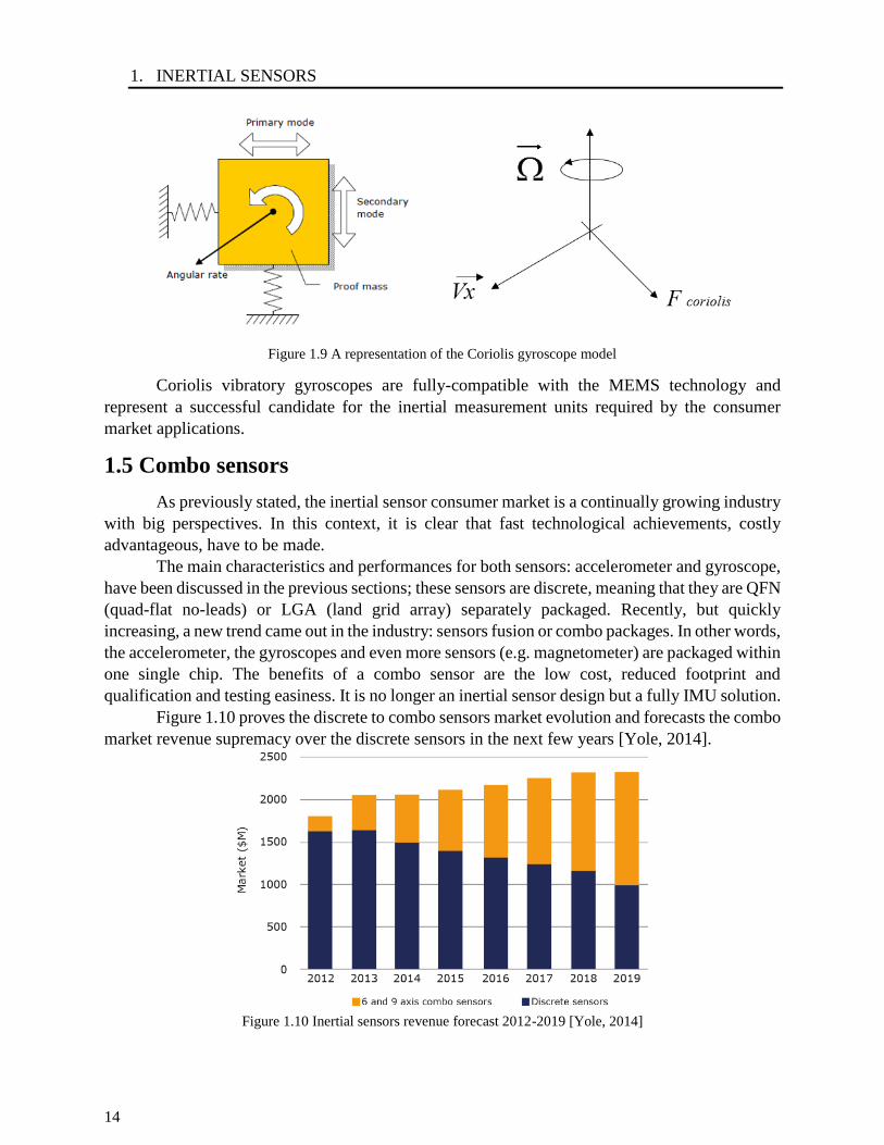
Figure 1.9 shows the resonator model of a Coriolis accelerometer: the primary vibrating
mode is induced electronically by a drive circuit while the secondary mode is driven by the Coriolis
force. The secondary mode oscillation amplitude is proportional to the angular velocity (1.1).
1. INERTIAL SENSORS
14
Figure 1.9 A representation of the Coriolis gyroscope model
Coriolis vibratory gyroscopes are fully-compatible with the MEMS technology and
represent a successful candidate for the inertial measurement units required by the consumer
market applications.
1.5 Combo sensors
As previously stated, the inertial sensor consumer market is a continually growing industry
with big perspectives. In this context, it is clear that fast technological achievements, costly
advantageous, have to be made.
The main characteristics and performances for both sensors: accelerometer and gyroscope,
have been discussed in the previous sections; these sensors are discrete, meaning that they are QFN
(quad-flat no-leads) or LGA (land grid array) separately packaged. Recently, but quickly
increasing, a new trend came out in the industry: sensors fusion or combo packages. In other words,
the accelerometer, the gyroscopes and even more sensors (e.g. magnetometer) are packaged within
one single chip. The benefits of a combo sensor are the low cost, reduced footprint and
qualification and testing easiness. It is no longer an inertial sensor design but a fully IMU solution.
Figure 1.10 proves the discrete to combo sensors market evolution and forecasts the combo
market revenue supremacy over the discrete sensors in the next few years [Yole, 2014].
Figure 1.10 Inertial sensors revenue forecast 2012-2019 [Yole, 2014]
1. INERTIAL SENSORS
15
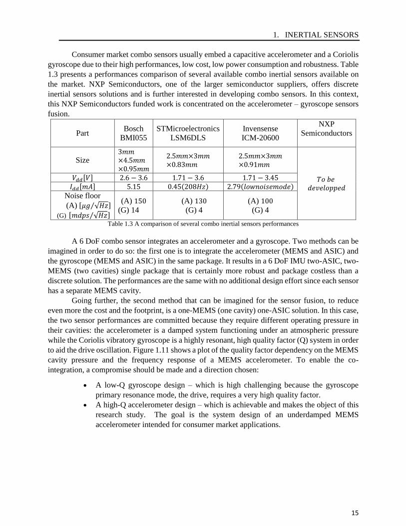
Consumer market combo sensors usually embed a capacitive accelerometer and a Coriolis
gyroscope due to their high performances, low cost, low power consumption and robustness. Table
1.3 presents a performances comparison of several available combo inertial sensors available on
the market. NXP Semiconductors, one of the larger semiconductor suppliers, offers discrete
inertial sensors solutions and is further interested in developing combo sensors. In this context,
this NXP Semiconductors funded work is concentrated on the accelerometer – gyroscope sensors
fusion.
Part Bosch
BMI055
STMicroelectronics
LSM6DLS
Invensense
ICM-20600
NXP
Semiconductors
Size
3𝑚𝑚×4.5𝑚𝑚×0.95𝑚𝑚
2.5𝑚𝑚×3𝑚𝑚×0.83𝑚𝑚
2.5𝑚𝑚×3𝑚𝑚×0.91𝑚𝑚
𝑇𝑜 𝑏𝑒 𝑑𝑒𝑣𝑒𝑙𝑜𝑝𝑝𝑒𝑑
𝑉𝑑𝑑[𝑉] 2.6 − 3.6 1.71 − 3.6 1.71 − 3.45
𝐼𝑑𝑑[𝑚𝐴] 5.15 0.45(208𝐻𝑧) 2.79(𝑙𝑜𝑤𝑛𝑜𝑖𝑠𝑒𝑚𝑜𝑑𝑒)
Noise floor
(A) [𝜇𝑔 √𝐻𝑧⁄ ]
(G) [𝑚𝑑𝑝𝑠 √𝐻𝑧⁄ ]
(A) 150
(G) 14
(A) 130
(G) 4
(A) 100
(G) 4
Table 1.3 A comparison of several combo inertial sensors performances
A 6 DoF combo sensor integrates an accelerometer and a gyroscope. Two methods can be
imagined in order to do so: the first one is to integrate the accelerometer (MEMS and ASIC) and
the gyroscope (MEMS and ASIC) in the same package. It results in a 6 DoF IMU two-ASIC, two-
MEMS (two cavities) single package that is certainly more robust and package costless than a
discrete solution. The performances are the same with no additional design effort since each sensor
has a separate MEMS cavity.
Going further, the second method that can be imagined for the sensor fusion, to reduce
even more the cost and the footprint, is a one-MEMS (one cavity) one-ASIC solution. In this case,
the two sensor performances are committed because they require different operating pressure in
their cavities: the accelerometer is a damped system functioning under an atmospheric pressure
while the Coriolis vibratory gyroscope is a highly resonant, high quality factor (Q) system in order
to aid the drive oscillation. Figure 1.11 shows a plot of the quality factor dependency on the MEMS
cavity pressure and the frequency response of a MEMS accelerometer. To enable the co-
integration, a compromise should be made and a direction chosen:
• A low-Q gyroscope design – which is high challenging because the gyroscope
primary resonance mode, the drive, requires a very high quality factor.
• A high-Q accelerometer design – which is achievable and makes the object of this
research study. The goal is the system design of an underdamped MEMS
accelerometer intended for consumer market applications.
1. INERTIAL SENSORS
16
Figure 1.11 A plot of the Quality factor (Q) vs. MEMS cavity pressure (left) and the frequency response of a second
order mass spring damper system (right)
From Figure 1.11, one can notice that a common cavity pressure lower than 1 torr is viable
for both sensors and can lead to a successful 6 DoF combo sensor design. Consequently, the
associated quality factor chosen for further designs and simulation, was considered to be superior
to 2000.
1.6 Summary
This chapter introduced the main inertial sensors applications and different types of motion.
Several accelerometer and gyroscope sensing principles with their associated performances have
been presented. The chapter also highlights the consumer market continuous development and the
increased combo sensors demand. Combo sensors usually embed a capacitive MEMS
accelerometer and a Coriolis gyroscope to provide a 6 DoF IMU. Further, a solution that allows
the accelerometer – gyroscope co-integration has been proposed and is based on the design of an
underdamped MEMS accelerometer.
Next chapter details the capacitive accelerometers and the electrostatic actuation
mechanism that appears in such transducers. A state of the art of the CMOS capacitive
accelerometers interfaces is also presented in Chapter 2.
17
CHAPTER 2
CMOS MEMS ACCELEROMETERS
The integration of MEMS accelerometers is a topic extensively researched over the past
years due to the sensors growing popularity and their new application fields. The integration efforts
have been concentrated around the sensor robustness, cost and power consumption reduction.
Additionally, to their high performances, the interest for the capacitive MEMS
accelerometers has also found its motivation in the electrostatic actuation capability. Whenever an
electrical potential is applied across the plates of a capacitor, an attractive force is generated across
the plates. For the accelerometers, this force is used to generate a force-balanced feedback, a
damping control or in self-test configurations.
Therefore, this chapter introduces the physics of the mechanical capacitive sensing
element, including the second order mass spring damper model, the electrostatic actuation
mechanism and its nonlinearities and the electrostatic spring forces.
Finally, an overview of the capacitive CMOS interfaces in the literature implementing
read-out techniques based on continuous-time voltage, continuous-time current and switched-
capacitor architectures, as well as the advantages and drawbacks for both open-loop and closed-
loop topologies using different control techniques, will be described in the next sections.
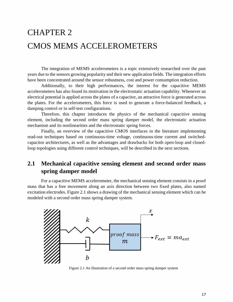
2.1 Mechanical capacitive sensing element and second order mass
spring damper model
For a capacitive MEMS accelerometer, the mechanical sensing element consists in a proof
mass that has a free movement along an axis direction between two fixed plates, also named
excitation electrodes. Figure 2.1 shows a drawing of the mechanical sensing element which can be
modeled with a second order mass spring damper system.
Figure 2.1 An illustration of a second order mass spring damper system
2. CMOS MEMS ACCELEROMETERS
18
When an external acceleration 𝑎𝑒𝑥𝑡 is applied on the proof mass 𝑚, an inertial force 𝐹𝑒𝑥𝑡
induces the proof mass displacement. The parameter 𝑘 is the spring coefficient, which is a sensor
design parameter and depends on the spring properties. The parameter 𝑏 is the mechanical
damping coefficient and depends both on the sensor structure and on the air pressure inside the
sensor cavity. Equation (2.1) can be derived from Figure 2.1, by applying the Newton’s second
law:
𝑚(𝑡) + 𝑏(𝑡) + 𝑘𝑥(𝑡) = 𝑚𝑎𝑒𝑥𝑡(𝑡) = 𝐹𝑒𝑥𝑡(𝑡) (2.1)
Where (𝑡) is the proof mass velocity and (𝑡) the proof mass acceleration. When the
steady state regime is reached, both (𝑡) and (𝑡) terms will be null and thus, eq. (2.1) can be
rewritten as:
𝑘𝑥 = 𝑚𝑎𝑒𝑥𝑡
𝑥
𝑎𝑒𝑥𝑡=
𝑚
𝑘= 𝐷𝑖𝑠𝑝𝑙𝑎𝑐𝑒𝑚𝑒𝑛𝑡 𝑠𝑒𝑛𝑠𝑖𝑡𝑖𝑣𝑖𝑡𝑦 (2.2)
The sensor has a continuous time movement, as expressed in equation (2.1), and therefore
to obtain the s-domain equivalent equation or the transfer function, the Laplace Transform can be
used. It will be shown later in this thesis that the mechanical sensing element transfer function can
also be reduced to a discrete-time equation when the architecture requires this approximation.
Equations (2.3) and (2.4) express the sensor transfer function when considering an inertial force
as input or acceleration, respectively:
𝐻𝑀𝐸𝑀𝑆(𝑥→𝐹)(𝑠) =𝑋(𝑠)
𝐹𝑒𝑥𝑡(𝑠)=
1/𝑚
𝑠2+𝑏
𝑚𝑠+
𝑘
𝑚
(2.3)
𝐻𝑀𝐸𝑀𝑆(𝑥→𝑎)(𝑠) =𝑋(𝑠)
𝑎𝑒𝑥𝑡(𝑠)=
1
𝑠2+𝑏
𝑚𝑠+
𝑘
𝑚
(2.4)
The natural pulsation of the transducer and the mechanical quality factor are:
𝜔𝑛 = √𝑘
𝑚 (2.5)
𝑄 =√𝑘𝑚
𝑏 (2.6)
If considering 𝜉 =1
2𝑄, the system transfer function becomes:
𝐻𝑀𝐸𝑀𝑆(𝑥→𝑎)(𝑠) =1
𝑠2+2𝜉𝜔𝑛𝑠+𝜔𝑛2 (2.7)
Depending on the quality factor level, one can define:
2. CMOS MEMS ACCELEROMETERS
19
• 𝑄 > 0.5 – the system is said underdamped or “high-Q”. The oscillations caused by
the high-quality factor are problematic when the oscillations amplitude is too large
and the electronic interface saturates, when due to the oscillations the proof mass
hits and sticks the sensor fingers but also when the proof mass settling times are too
long for certain applications. All the above-mentioned drawbacks can be overcome
with the aid of an artificial electrical damping mechanism.
• 𝑄 = 0.5 – the system is critically damped. For this specific case, the settling time
is minimum.
• 𝑄 < 0.5 – the system is overdamped. No special caution needs to be taken to
control the transducer.
Consequently, it was shown that the capacitive accelerometer sensor model can be reduced
to a second order mass spring damper system with a continuous time transfer function which
depends on several transducer design parameters. The behavior of the MEMS can be anticipated
by evaluating its quality factor.
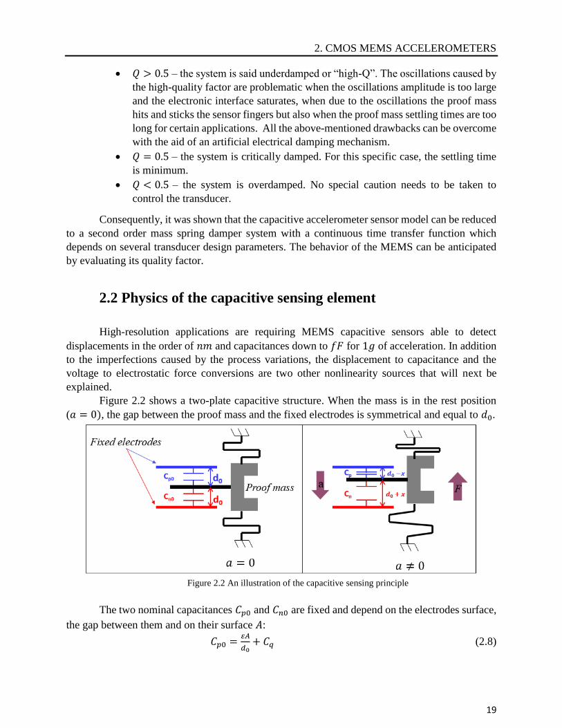
2.2 Physics of the capacitive sensing element
High-resolution applications are requiring MEMS capacitive sensors able to detect
displacements in the order of 𝑛𝑚 and capacitances down to 𝑓𝐹 for 1𝑔 of acceleration. In addition
to the imperfections caused by the process variations, the displacement to capacitance and the
voltage to electrostatic force conversions are two other nonlinearity sources that will next be
explained.
Figure 2.2 shows a two-plate capacitive structure. When the mass is in the rest position
(𝑎 = 0), the gap between the proof mass and the fixed electrodes is symmetrical and equal to 𝑑0.
Figure 2.2 An illustration of the capacitive sensing principle
The two nominal capacitances 𝐶𝑝0 and 𝐶𝑛0 are fixed and depend on the electrodes surface,
the gap between them and on their surface 𝐴:
𝐶𝑝0 =𝜀𝐴
𝑑0+ 𝐶𝑞 (2.8)
2. CMOS MEMS ACCELEROMETERS
20
𝐶𝑛0 =𝜀𝐴
𝑑0+ 𝐶𝑞 (2.9)
where 𝜀 is the air permittivity and 𝐶𝑞 a parasitic fixed capacitance.
When the proof mass is deflected under the effect of an extern acceleration, one of the fixed
nominal capacitance will increase while the other decreases:
𝐶𝑝 =𝜀𝐴
𝑑0−𝑥+ 𝐶𝑞 (2.10)
𝐶𝑛 =𝜀𝐴
𝑑0+𝑥+ 𝐶𝑞 (2.11)
Then, the capacitance variations ∆𝐶𝑝, ∆𝐶𝑛 can be deduced as:
∆𝐶𝑝 = 𝐶𝑝 − 𝐶𝑝0 =𝜀𝐴
𝑑0×
𝑥
𝑑0×
1
(1− 𝑥
𝑑0) (2.12)
∆𝐶𝑛 = 𝐶𝑛 − 𝐶𝑛0 =𝜀𝐴
𝑑0×
𝑥
𝑑0×
1
(1+ 𝑥
𝑑0) (2.13)
Using the Taylor development for the geometric series 1
1 ± 𝑥
𝑑0
and considering that the
displacement 𝑥 is much smaller than the gap between the electrodes 𝑑0, one can find that the
overall capacitance variation is proportional to x as:
∆𝐶 = ∆𝐶𝑝 + ∆𝐶𝑛 ≈2𝜀𝐴
𝑑0×
𝑥
𝑑0 (2.14)
However, the relationship (2.14) is only an approximation and the capacitance variation
∆𝐶 is only proportional to the MEMS displacement within a limited range of operation where
𝑥
𝑑0≪ 1 . Figure 2.3 illustrates the capacitance variation of a transducer with a sensitivity of
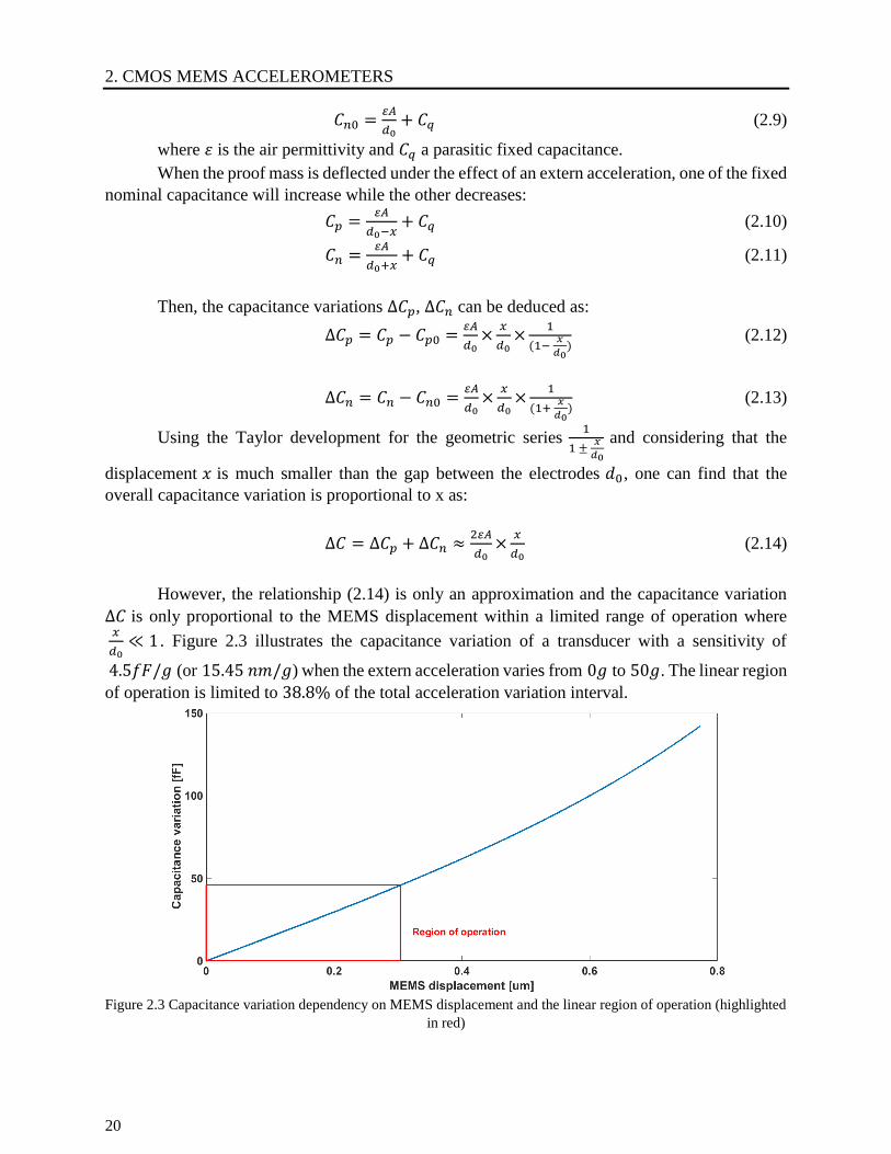
4.5𝑓𝐹/𝑔 (or 15.45 𝑛𝑚/𝑔) when the extern acceleration varies from 0𝑔 to 50𝑔. The linear region
of operation is limited to 38.8% of the total acceleration variation interval.
Figure 2.3 Capacitance variation dependency on MEMS displacement and the linear region of operation (highlighted
in red)
2. CMOS MEMS ACCELEROMETERS
21
In addition to the nonlinear capacitance, when the displacement is increasing the sensor
can experience the spring softening effect, further explained.
2.3 Electrostatic actuation
During the past years, high performances micro actuators have been developed and
integrated in many domains as the automotive industry or in biomedical applications [Park, 2011].
Several actuation mechanisms have been heavily researched due to the easiness they can be used
within typical MEMS technologies and will be next be presented.
The electromagnetic actuation uses a ferromagnetic material to displace the microactuator
[Iseki, 2006] and even if provides the highest displacement comparing with the others actuation
methods, has a complicated fabrication process and consumes high power. The piezoelectric
actuation occurs when an electric field is applied across a piezoelectric material [Robbins, 1991].
It consumes lower power and has a good linearity [Seo, 2005]. Another method is the
electrothermal actuation that uses the expansion of some solids or fluids under the temperature
effect to move the microactuator. The electrothermal actuation has a simple fabrication method
but very slow responses times [Atre, 2006].
2.3.1 Electrostatic actuation mechanism
Finally, the electrostatic actuation uses the attraction force (e.g. electrostatic force) between
two oppositely charged plates when a voltage 𝑉 is applied across them to displace the
microactuator. The main advantages of the electrostatic actuation are the possibility to design both
the sensing and microactuator device using typical CMOS and MEMS technologies, the low power
consumption and also the high speed since it is based on the capacitors charge-discharge
mechanism. The drawbacks are that the electrostatic force is inversely proportional to the square
of the actuator displacement which leads to large force value only when the distance is small and
a limited operation range due to the spring softening effect when high actuation voltage is applied
resulting in nonlinear forces.
To find the electrostatic force 𝐹𝑒𝑙 expression, one has to consider the energy 𝐸 stored in
the capacitance that exists between the two oppositely charged plates:
E =1
2𝐶𝑉2 =
1
2
𝜀𝐴
𝑑𝑉2 (2.15)
𝐹𝑒𝑙 =𝜕𝐸
𝜕𝑑= −
1
2
𝜀𝐴
𝑑2 𝑉2 (2.16)
The electrostatic actuation is also the most popular actuation method due to the diversity
of the control techniques that can be used to implement the actuation. Conventional electrostatic
actuation uses voltage and charge control [Seeger, 2003] but a combination of the voltage control
with a feedback capacitor can also be considered [Chan, 2000], [Maithripala, 2003]. Further, more
recent research works proved the efficiency of a parallel plate actuator driven by a resonant circuit
[Kyynäräinen, 2001], [Cagdaser, 2005].
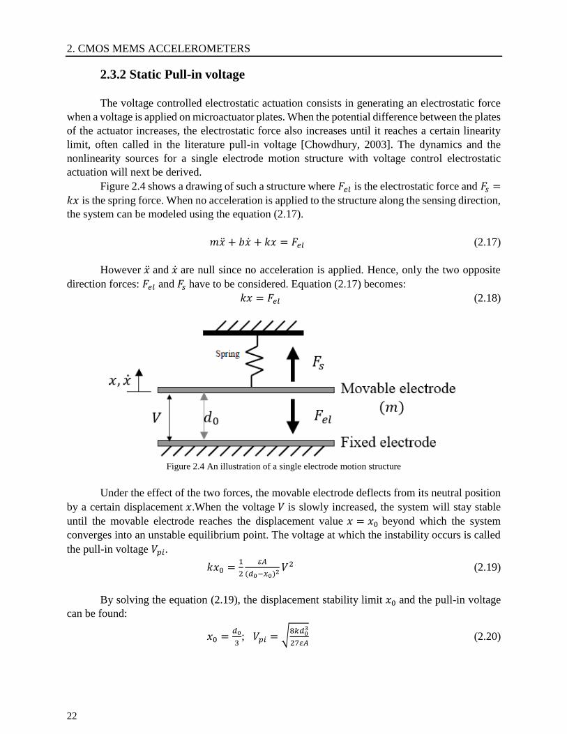
2. CMOS MEMS ACCELEROMETERS
22
2.3.2 Static Pull-in voltage
The voltage controlled electrostatic actuation consists in generating an electrostatic force
when a voltage is applied on microactuator plates. When the potential difference between the plates
of the actuator increases, the electrostatic force also increases until it reaches a certain linearity
limit, often called in the literature pull-in voltage [Chowdhury, 2003]. The dynamics and the
nonlinearity sources for a single electrode motion structure with voltage control electrostatic
actuation will next be derived.
Figure 2.4 shows a drawing of such a structure where 𝐹𝑒𝑙 is the electrostatic force and 𝐹𝑠 =
𝑘𝑥 is the spring force. When no acceleration is applied to the structure along the sensing direction,
the system can be modeled using the equation (2.17).
𝑚 + 𝑏 + 𝑘𝑥 = 𝐹𝑒𝑙 (2.17)
However and are null since no acceleration is applied. Hence, only the two opposite
direction forces: 𝐹𝑒𝑙 and 𝐹𝑠 have to be considered. Equation (2.17) becomes:
𝑘𝑥 = 𝐹𝑒𝑙 (2.18)
Figure 2.4 An illustration of a single electrode motion structure
Under the effect of the two forces, the movable electrode deflects from its neutral position
by a certain displacement 𝑥.When the voltage 𝑉 is slowly increased, the system will stay stable
until the movable electrode reaches the displacement value 𝑥 = 𝑥0 beyond which the system
converges into an unstable equilibrium point. The voltage at which the instability occurs is called
the pull-in voltage 𝑉𝑝𝑖.
𝑘𝑥0 =1
2
𝜀𝐴
(𝑑0−𝑥0)2 𝑉2 (2.19)
By solving the equation (2.19), the displacement stability limit 𝑥0 and the pull-in voltage
can be found:
𝑥0 =𝑑0
3; 𝑉𝑝𝑖 = √8𝑘𝑑0
3
27𝜀𝐴 (2.20)
2. CMOS MEMS ACCELEROMETERS
23
When the voltage 𝑉 is equal or greater than 𝑉𝑝𝑖, the movable electrode snaps into contact
with the fixed electrode. This happens because the electrostatic force is larger than the spring
force. Therefore, for an open-loop architecture, with no control over the proof mass movement,
the transducer has a limited linear range of operation reached once the displacement closes 𝑥0.
Several methods have been investigated to increase the linear range of operation [Seeger, 1997],
[Chan, 2000], however they usually need higher operating voltage.
2.3.3 Spring softening effect
Another nonlinear effect that appears in capacitive MEMS sensors is the spring softening
effect [Mukherjee, 2011] and consists in slightly modifying the spring mechanical constant 𝑘 due
to the second order components of the electrostatic force. Hence, the spring softening effect leads
to a sensitivity and resonance frequency alteration.
Equation (2.19) can be rewritten as:
𝑘𝑥 =𝜀𝐴
2𝑑02
1
(1−𝑥
𝑑0)2
𝑉2 (2.21)
Where 𝑥 is the proof mass displacement under the effect of the electrostatic force.
After developing the series 1
(1−𝑥
𝑑0)2
using the Taylor relationship, the overall net force
applied to the transducer becomes:
∆𝐹 = 𝑘𝑥 −𝜀𝐴
2𝑑02 𝑉2(1 +
2𝑥
𝑑0) (2.22)
∆𝐹 = 𝑥 (𝑘 −𝜀𝐴𝑉2
𝑑03 ) +
𝜀𝐴
2𝑑02 𝑉2 (2.23)
It can be noticed from equation (2.22) that the mechanical constant 𝑘 is decreased by a
term called 𝑘𝑠𝑜𝑓𝑡 =𝜀𝐴𝑉2
𝑑03 .
Depending on the actuation voltage and on the gap between electrodes, the spring softening
constant can slightly influence the sensitivity and the resonance pulsation:
𝜔𝑟𝑒𝑠 = √1
𝑚(𝑘 − 𝑘𝑠𝑜𝑓𝑡) (2.24)
𝑆 =𝑚
𝑘−𝑘𝑠𝑜𝑓𝑡 (2.25)
The spring softening effect appears also in a three-plate structure electrostatically actuated
[Xie, 2003] since the spring softening constant results from the second-order terms of the
electrostatic force. Figure 2.5 shows such a structure where 𝑉0 is the actuation voltage and 𝑉𝑥 the
voltage applied on the movable electrode. The difference of the two electrostatic forces applied on
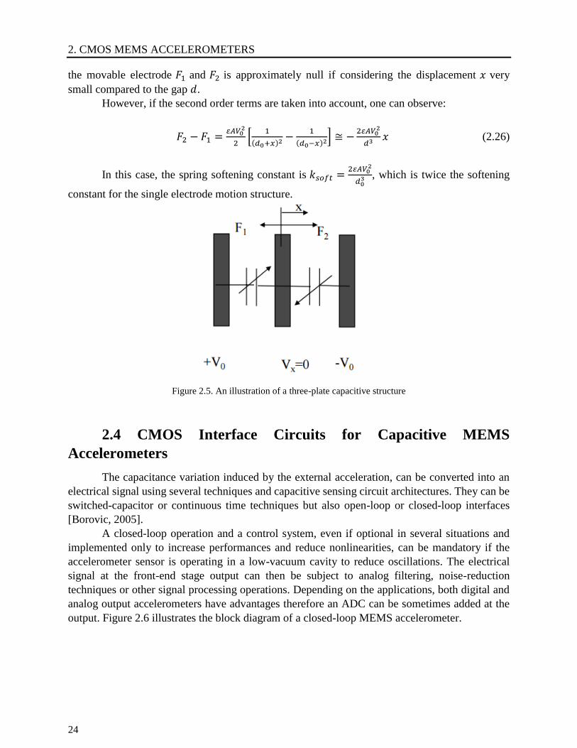
2. CMOS MEMS ACCELEROMETERS
24
the movable electrode 𝐹1 and 𝐹2 is approximately null if considering the displacement 𝑥 very
small compared to the gap 𝑑.
However, if the second order terms are taken into account, one can observe:
𝐹2 − 𝐹1 =𝜀𝐴𝑉0
2
2[
1
(𝑑0+𝑥)2 −1
(𝑑0−𝑥)2] ≅ −2𝜀𝐴𝑉0
2
𝑑3 𝑥 (2.26)
In this case, the spring softening constant is 𝑘𝑠𝑜𝑓𝑡 =2𝜀𝐴𝑉0
2
𝑑03 , which is twice the softening
constant for the single electrode motion structure.
Figure 2.5. An illustration of a three-plate capacitive structure
2.4 CMOS Interface Circuits for Capacitive MEMS
Accelerometers
The capacitance variation induced by the external acceleration, can be converted into an
electrical signal using several techniques and capacitive sensing circuit architectures. They can be
switched-capacitor or continuous time techniques but also open-loop or closed-loop interfaces
[Borovic, 2005].
A closed-loop operation and a control system, even if optional in several situations and
implemented only to increase performances and reduce nonlinearities, can be mandatory if the
accelerometer sensor is operating in a low-vacuum cavity to reduce oscillations. The electrical
signal at the front-end stage output can then be subject to analog filtering, noise-reduction
techniques or other signal processing operations. Depending on the applications, both digital and
analog output accelerometers have advantages therefore an ADC can be sometimes added at the
output. Figure 2.6 illustrates the block diagram of a closed-loop MEMS accelerometer.
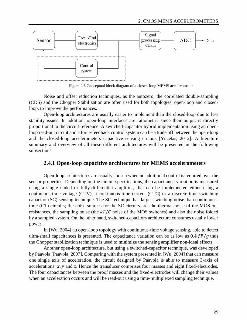
2. CMOS MEMS ACCELEROMETERS
25
Figure 2.6 Conceptual block diagram of a closed-loop MEMS accelerometer
Noise and offset reduction techniques, as the autozero, the correlated double-sampling
(CDS) and the Chopper Stabilization are often used for both topologies, open-loop and closed-
loop, to improve the performances.
Open-loop architectures are usually easier to implement than the closed-loop due to less
stability issues. In addition, open-loop interfaces are ratiometric since their output is directly
proportional to the circuit reference. A switched-capacitor hybrid implementation using an open-
loop read-out circuit and a force-feedback control system can be a trade off between the open-loop
and the closed-loop accelerometers capacitive sensing circuits [Yucetas, 2012]. A literature
summary and overview of all these different architectures will be presented in the following
subsections.
2.4.1 Open-loop capacitive architectures for MEMS accelerometers
Open-loop architectures are usually chosen when no additional control is required over the
sensor properties. Depending on the circuit specifications, the capacitance variation is measured
using a single ended or fully-differential amplifier, that can be implemented either using a
continuous-time voltage (CTV), a continuous-time current (CTC) or a discrete-time switching
capacitor (SC) sensing technique. The SC technique has larger switching noise than continuous-
time (CT) circuits; the noise sources for the SC circuits are: the thermal noise of the MOS on-
resistances, the sampling noise (the 𝑘𝑇/𝐶 noise of the MOS switches) and also the noise folded
by a sampled system. On the other hand, switched-capacitors architecture consumes usually lower
power.
In [Wu, 2004] an open-loop topology with continuous-time voltage sensing, able to detect
ultra-small capacitances is presented. The capacitance variation can be as low as 0.4 𝑓𝐹/𝑔 thus
the Chopper stabilization technique is used to minimize the sensing amplifier non-ideal effects.
Another open-loop architecture, but using a switched-capacitor technique, was developed
by Paavola [Paavola, 2007]. Comparing with the system presented in [Wu, 2004] that can measure
one single axis of acceleration, the circuit designed by Paavola is able to measure 3-axis of
accelerations: 𝑥, 𝑦 and 𝑧. Hence the transducer comprises four masses and eight fixed-electrodes.
The four capacitances between the proof masses and the fixed-electrodes will change their values
when an acceleration occurs and will be read-out using a time-multiplexed sampling technique.
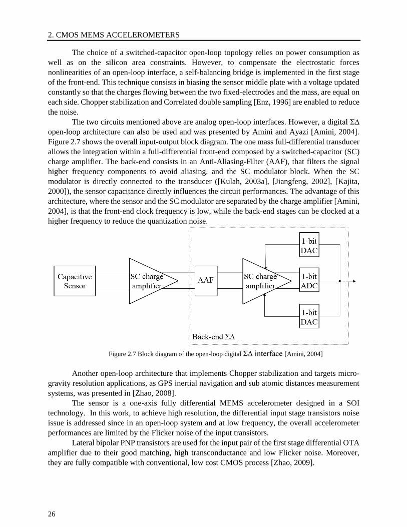
2. CMOS MEMS ACCELEROMETERS
26
The choice of a switched-capacitor open-loop topology relies on power consumption as
well as on the silicon area constraints. However, to compensate the electrostatic forces
nonlinearities of an open-loop interface, a self-balancing bridge is implemented in the first stage
of the front-end. This technique consists in biasing the sensor middle plate with a voltage updated
constantly so that the charges flowing between the two fixed-electrodes and the mass, are equal on
each side. Chopper stabilization and Correlated double sampling [Enz, 1996] are enabled to reduce
the noise.
The two circuits mentioned above are analog open-loop interfaces. However, a digital Σ∆
open-loop architecture can also be used and was presented by Amini and Ayazi [Amini, 2004].
Figure 2.7 shows the overall input-output block diagram. The one mass full-differential transducer
allows the integration within a full-differential front-end composed by a switched-capacitor (SC)
charge amplifier. The back-end consists in an Anti-Aliasing-Filter (AAF), that filters the signal
higher frequency components to avoid aliasing, and the SC modulator block. When the SC
modulator is directly connected to the transducer ([Kulah, 2003a], [Jiangfeng, 2002], [Kajita,
2000]), the sensor capacitance directly influences the circuit performances. The advantage of this
architecture, where the sensor and the SC modulator are separated by the charge amplifier [Amini,
2004], is that the front-end clock frequency is low, while the back-end stages can be clocked at a
higher frequency to reduce the quantization noise.
Figure 2.7 Block diagram of the open-loop digital Σ∆ interface [Amini, 2004]
Another open-loop architecture that implements Chopper stabilization and targets micro-
gravity resolution applications, as GPS inertial navigation and sub atomic distances measurement
systems, was presented in [Zhao, 2008].
The sensor is a one-axis fully differential MEMS accelerometer designed in a SOI
technology. In this work, to achieve high resolution, the differential input stage transistors noise
issue is addressed since in an open-loop system and at low frequency, the overall accelerometer
performances are limited by the Flicker noise of the input transistors.
Lateral bipolar PNP transistors are used for the input pair of the first stage differential OTA
amplifier due to their good matching, high transconductance and low Flicker noise. Moreover,
they are fully compatible with conventional, low cost CMOS process [Zhao, 2009].
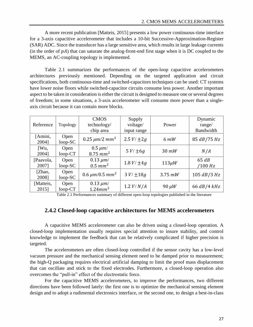
2. CMOS MEMS ACCELEROMETERS
27
A more recent publication [Matteis, 2015] presents a low power continuous-time interface
for a 3-axis capacitive accelerometer that includes a 10-bit Successive-Approximation-Register
(SAR) ADC. Since the transducer has a large sensitive area, which results in large leakage currents
(in the order of 𝑝𝐴) that can saturate the analog-front-end first stage when it is DC coupled to the
MEMS, an AC-coupling topology is implemented.
Table 2.1 summarizes the performances of the open-loop capacitive accelerometers
architectures previously mentioned. Depending on the targeted application and circuit
specifications, both continuous-time and switched-capacitors techniques can be used: CT systems
have lower noise floors while switched-capacitor circuits consume less power. Another important
aspect to be taken in consideration is either the circuit is designed to measure one or several degrees
of freedom; in some situations, a 3-axis accelerometer will consume more power than a single-
axis circuit because it can contain more blocks.
Reference Topology
CMOS
technology/
chip area
Supply
voltage/
input range
Power
Dynamic
range/
Bandwidth
[Amini,
2004]
Open
loop-SC 0.25 𝜇𝑚/2 𝑚𝑚2 2.5 𝑉/ ±2𝑔 6 𝑚𝑊 85 𝑑𝐵/75 𝐻𝑧
[Wu,
2004]
Open
loop-CT
0.5 𝜇𝑚/
8.75 𝑚𝑚2 5 𝑉/ ±6𝑔 30 𝑚𝑊 𝑁/𝐴
[Paavola,
2007]
Open
loop-SC
0.13 𝜇𝑚/
0.5 𝑚𝑚2 1.8 𝑉/ ±4𝑔 113𝜇𝑊
65 𝑑𝐵/100 𝐻𝑧
[Zhao,
2008]
Open
loop-SC 0.6 𝜇𝑚/0.5 𝑚𝑚2 3 𝑉/ ±18𝑔 3.75 𝑚𝑊 105 𝑑𝐵/3 𝐻𝑧
[Matteis,
2015]
Open
loop-CT
0.13 𝜇𝑚/
1.24𝑚𝑚2 1.2 𝑉/ 𝑁/𝐴 90 𝜇𝑊 66 𝑑𝐵/4 𝑘𝐻𝑧
Table 2.1 Performances summary of different open-loop topologies published in the literature
2.4.2 Closed-loop capacitive architectures for MEMS accelerometers
A capacitive MEMS accelerometer can also be driven using a closed-loop operation. A
closed-loop implementation usually requires special attention to insure stability, and control
knowledge to implement the feedback that can be relatively complicated if higher precision is
targeted.
The accelerometers are often closed-loop controlled if the sensor cavity has a low-level
vacuum pressure and the mechanical sensing element need to be damped prior to measurement;
the high-Q packaging requires electrical artificial damping to limit the proof mass displacement
that can oscillate and stick to the fixed electrodes. Furthermore, a closed-loop operation also
overcomes the “pull-in” effect of the electrostatic force.
For the capacitive MEMS accelerometers, to improve the performances, two different
directions have been followed lately: the first one is to optimize the mechanical sensing element
design and to adopt a rudimental electronics interface, or the second one, to design a best-in-class
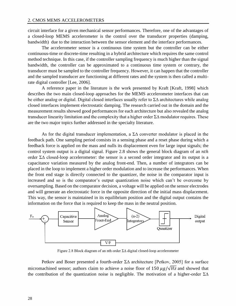
2. CMOS MEMS ACCELEROMETERS
28
circuit interface for a given mechanical sensor performances. Therefore, one of the advantages of
a closed-loop MEMS accelerometer is the control over the transducer properties (damping,
bandwidth) due to the interaction between the sensor element and the interface performances.
The accelerometer sensor is a continuous time system but the controller can be either
continuous-time or discrete-time resulting in a hybrid architecture which requires the same control
method technique. In this case, if the controller sampling frequency is much higher than the signal
bandwidth, the controller can be approximated to a continuous time system or contrary, the
transducer must be sampled to the controller frequency. However, it can happen that the controller
and the sampled transducer are functioning at different rates and the system is then called a multi-
rate digital controller [Lee, 2006].
A reference paper in the literature is the work presented by Kraft [Kraft, 1998] which
describes the two main closed-loop approaches for the MEMS accelerometer interfaces that can
be either analog or digital. Digital closed interfaces usually refer to Σ∆ architectures while analog
closed interfaces implement electrostatic damping. The research carried out in the domain and the
measurement results showed good performances for each architecture but also revealed the analog
transducer linearity limitation and the complexity that a higher order Σ∆ modulator requires. These
are the two major topics further addressed in the specialty literature.
As for the digital transducer implementation, a Σ∆ converter modulator is placed in the
feedback path. One sampling period consists in a sensing phase and a reset phase during which a
feedback force is applied on the mass and nulls its displacement even for large input signals; the
control system output is a digital signal. Figure 2.8 shows the general block diagram of an 𝑛𝑡ℎ
order Σ∆ closed-loop accelerometer: the sensor is a second order integrator and its output is a
capacitance variation measured by the analog front-end. Then, a number of integrators can be
placed in the loop to implement a higher order modulation and to increase the performances. When
the front end stage is directly connected to the quantizer, the noise in the comparator input is
increased and so is the comparator’s output quantization noise which can’t be overcome by
oversampling. Based on the comparator decision, a voltage will be applied on the sensor electrodes
and will generate an electrostatic force in the opposite direction of the initial mass displacement.
This way, the sensor is maintained in its equilibrium position and the digital output contains the
information on the force that is required to keep the mass in the neutral position.
Figure 2.8 Block diagram of an nth order Σ∆ digital closed-loop accelerometer
Petkov and Boser presented a fourth-order Σ∆ architecture [Petkov, 2005] for a surface
micromachined sensor; authors claim to achieve a noise floor of 150 𝜇𝑔/√𝐻𝑧 and showed that
the contribution of the quantization noise is negligible. The motivation of a higher-order Σ∆
2. CMOS MEMS ACCELEROMETERS
29
modulation is to decrease the quantization noise which is generally much larger than the analog-
front end electronic noise [Kulah, 2006]. Comparing with a second order Σ∆ capacitive
accelerometer ([Lu, 1995], [Lemkin, 1999], [Jiang, 2000], [Kulah, 2002]) that uses only the
second-order sensor element as loop-filter, this work presents a single-loop high-order Σ∆
architecture, based on two integrators with feedforward summation.
A higher-order Σ∆ modulator for a closed-loop accelerometer was also reported by Chen
[Chen, 2014]. The sensor has a low vacuum packaging which allows the co-integration within a
gyroscope but requires a method to reduce the settling times and the ringing. The configuration
proposed in this paper has the second order mechanical sensing element part of the loop, four
electronic integrators cascaded in the multi-feedback loops and a quantizer block, which results in
a sixth-order Σ∆ continuous time interface. The system output is digitalized and there is no need
for an additional ADC. However, here, separate electrodes for the sensing and for the feedback are
used to enable the design of a damping system that can reduce the oscillations due to vacuum
packaging.
Another closed-loop, most recent, Σ∆ interface for a high Q capacitive surface
micromachined sensor was reported by Xu [Xu, 2015]. Sub − 𝜇𝑔 − resolution is obtained
implementing the switching-capacitor technique and increasing the Σ∆ modulator order to three,
resulting in an overall fifth-order system. The transducer does not have dedicated electrodes for
the force feedback phase during which the sensor is damped, thus a time-multiplexing chronogram
was conceived. Low-noise design techniques, as the CDS, have been used for the analog-front-
end. Similar Σ∆ modulator interfaces with high performances can be found in the literature
[Paavola, 2009], [Pastre, 2009], [Lang, 1999], [Lajevardi, 2012], [Petkov, 2014], [Wang, 2015],
however, the main drawbacks of the digital loops remain the power consumption caused by the
system complexity and the stability issue. Additionally, for a multiples degrees of freedom sensor,
the Σ∆ interface can be used only if the movable electrode is not shared between several axes.
Furthermore, regarding the analog closed loop interfaces for capacitive accelerometers, the
research interest has been concentrated around the electrostatic forces linearity for a higher input
dynamic range but also the control over the sensor properties when low-vacuum operation is
required. High resolution and low power applications can also be targeted with an analog loop
implementation.
Considering now the analog transducer presented in Figure 2.9, when functioning in
closed-loop, two electrostatic forces will be superimposed on the proof mass, to provide a linear
operation. The net electrostatic force applied to the transducer is proportional to the output 𝑉𝑜𝑢𝑡
and to 𝑉𝐵 when the mass displacement is very small compared with the gap between the electrodes.
To increase the linear operation range a higher DC voltage 𝑉𝐵 can be applied. The electrostatic
damping principle will be detailed in the next chapter.
Analog closed-loop interfaces can also be continuous-time [Aaltonen, 2007] or switched-
capacitors circuits [Yin, 2009], [Zhao, 2016]. In [Aaltonen, 2007] a proportional-integrator-
derivative (PID) control block is used to damp the high Q transducer. Techniques as CDS or the
use of n-type bipolar transistors for the input of the analog front-end first stage can be used for
noise considerations.
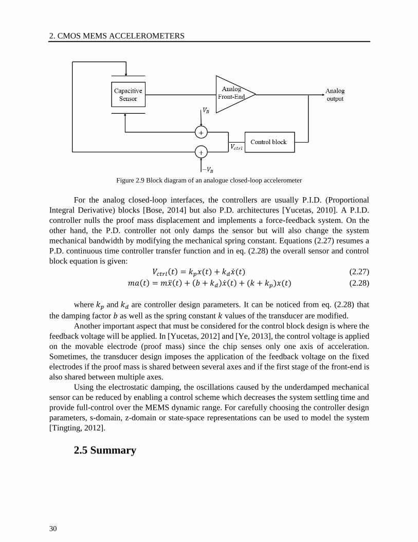
2. CMOS MEMS ACCELEROMETERS
30
Figure 2.9 Block diagram of an analogue closed-loop accelerometer
For the analog closed-loop interfaces, the controllers are usually P.I.D. (Proportional
Integral Derivative) blocks [Bose, 2014] but also P.D. architectures [Yucetas, 2010]. A P.I.D.
controller nulls the proof mass displacement and implements a force-feedback system. On the
other hand, the P.D. controller not only damps the sensor but will also change the system
mechanical bandwidth by modifying the mechanical spring constant. Equations (2.27) resumes a
P.D. continuous time controller transfer function and in eq. (2.28) the overall sensor and control
block equation is given:
𝑉𝑐𝑡𝑟𝑙(𝑡) = 𝑘𝑝𝑥(𝑡) + 𝑘𝑑(𝑡) (2.27)
𝑚𝑎(𝑡) = 𝑚(𝑡) + (𝑏 + 𝑘𝑑)(𝑡) + (𝑘 + 𝑘𝑝)𝑥(𝑡) (2.28)
where 𝑘𝑝 and 𝑘𝑑 are controller design parameters. It can be noticed from eq. (2.28) that
the damping factor 𝑏 as well as the spring constant 𝑘 values of the transducer are modified.
Another important aspect that must be considered for the control block design is where the
feedback voltage will be applied. In [Yucetas, 2012] and [Ye, 2013], the control voltage is applied
on the movable electrode (proof mass) since the chip senses only one axis of acceleration.
Sometimes, the transducer design imposes the application of the feedback voltage on the fixed
electrodes if the proof mass is shared between several axes and if the first stage of the front-end is
also shared between multiple axes.
Using the electrostatic damping, the oscillations caused by the underdamped mechanical
sensor can be reduced by enabling a control scheme which decreases the system settling time and
provide full-control over the MEMS dynamic range. For carefully choosing the controller design
parameters, s-domain, z-domain or state-space representations can be used to model the system
[Tingting, 2012].
2.5 Summary
2. CMOS MEMS ACCELEROMETERS
31
This chapter resumed the physics of the capacitive sensor as well as the electrostatic
actuation mechanism and its associated nonlinearities. It was highlighted the importance of the
mathematical modeling of each block, part of the CMOS MEMS accelerometer system.
The mechanical sensing element can be modeled using the second-order mass spring
damper transfer function. The continuous-time model can then be transformed in a discrete-time
system with a certain frequency rate if required. The mechanical damping ratio depends on the
spring design and on the cavity pressure around the sensor. If the sensor is underdamped, it will
start oscillating and in order to rapidly decrease the oscillations amplitude, the mechanical
damping can be adjusted electrostatically.
The electrostatic actuation mechanism has been presented. The voltage applied across a
charged capacitor will generate an electrostatic force which can be used to increase the mechanical
damping. The electrostatic force has a second order dependency with the gap between the
electrodes, the proof mass displacement and with the actuation voltage. The spring softening and
the pull-in effect have been discussed. The pull-in effect can produce the snapping of the movable
electrode onto the fixed plate if either the actuation voltage or the gap between the electrodes are
not controlled; hence, the importance of the closed-loop systems.
Switched-capacitor, continuous time voltage or current techniques can be used for the
capacitance read-out. Capacitive open-loop systems are easy to implement, they don’t have
stability issues and consume less power. Moreover, they have a ratiometric output. On the other
hand, closed-loop systems can achieve larger signal bandwidth, high input range and higher
linearity. Digital interfaces have the advantage of direct digitized data output while complex
implementations. Analog interfaces are consuming less power but have linearity limitations. The
main privilege of a closed-loop implementation is the artificial damping control which is highly
recommended when the sensor is operating in high-vacuum cavity.
Table 2.2 presents a summary of the performances and architectures of the published
capacitive MEMS accelerometers discussed in previous sections, where O refers to an open-loop
architecture and C to a closed-loop architecture.
In next chapter, a novel closed-loop electrostatic damping architecture for a three-axis
underdamped accelerometer will be presented. The system is a switched-capacitors discrete
architecture with simultaneous electrostatic damping control. Matlab-Simulink models and z-
Transform transfer functions have been developed for each block. Finally, a new approach to
establish the system closed-loop transfer function and to study the stability is presented.
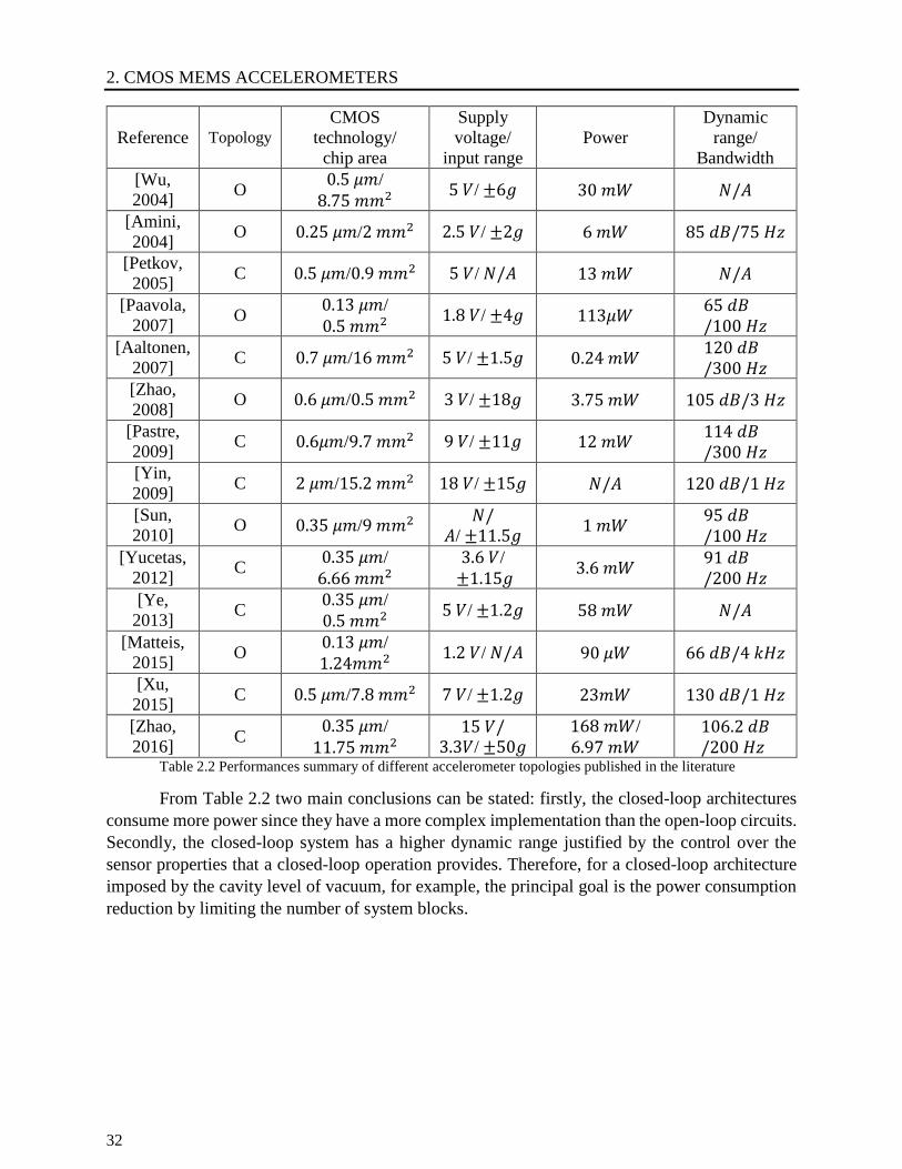
2. CMOS MEMS ACCELEROMETERS
32
Reference Topology
CMOS
technology/
chip area
Supply
voltage/
input range
Power
Dynamic
range/
Bandwidth
[Wu,
2004] O
0.5 𝜇𝑚/
8.75 𝑚𝑚2 5 𝑉/ ±6𝑔 30 𝑚𝑊 𝑁/𝐴
[Amini,
2004] O 0.25 𝜇𝑚/2 𝑚𝑚2 2.5 𝑉/ ±2𝑔 6 𝑚𝑊 85 𝑑𝐵/75 𝐻𝑧
[Petkov,
2005] C 0.5 𝜇𝑚/0.9 𝑚𝑚2 5 𝑉/ 𝑁/𝐴 13 𝑚𝑊 𝑁/𝐴
[Paavola,
2007] O
0.13 𝜇𝑚/
0.5 𝑚𝑚2 1.8 𝑉/ ±4𝑔 113𝜇𝑊
65 𝑑𝐵/100 𝐻𝑧
[Aaltonen,
2007] C 0.7 𝜇𝑚/16 𝑚𝑚2 5 𝑉/ ±1.5𝑔 0.24 𝑚𝑊
120 𝑑𝐵/300 𝐻𝑧
[Zhao,
2008] O 0.6 𝜇𝑚/0.5 𝑚𝑚2 3 𝑉/ ±18𝑔 3.75 𝑚𝑊 105 𝑑𝐵/3 𝐻𝑧
[Pastre,
2009] C 0.6𝜇𝑚/9.7 𝑚𝑚2 9 𝑉/ ±11𝑔 12 𝑚𝑊
114 𝑑𝐵/300 𝐻𝑧
[Yin,
2009] C 2 𝜇𝑚/15.2 𝑚𝑚2 18 𝑉/ ±15𝑔 𝑁/𝐴 120 𝑑𝐵/1 𝐻𝑧
[Sun,
2010] O 0.35 𝜇𝑚/9 𝑚𝑚2
𝑁/𝐴/ ±11.5𝑔
1 𝑚𝑊 95 𝑑𝐵/100 𝐻𝑧
[Yucetas,
2012] C
0.35 𝜇𝑚/
6.66 𝑚𝑚2
3.6 𝑉/
±1.15𝑔 3.6 𝑚𝑊
91 𝑑𝐵/200 𝐻𝑧
[Ye,
2013] C
0.35 𝜇𝑚/
0.5 𝑚𝑚2 5 𝑉/ ±1.2𝑔 58 𝑚𝑊 𝑁/𝐴
[Matteis,
2015] O
0.13 𝜇𝑚/
1.24𝑚𝑚2 1.2 𝑉/ 𝑁/𝐴 90 𝜇𝑊 66 𝑑𝐵/4 𝑘𝐻𝑧
[Xu,
2015] C 0.5 𝜇𝑚/7.8 𝑚𝑚2 7 𝑉/ ±1.2𝑔 23𝑚𝑊 130 𝑑𝐵/1 𝐻𝑧
[Zhao,
2016] C
0.35 𝜇𝑚/
11.75 𝑚𝑚2
15 𝑉/3.3𝑉/ ±50𝑔
168 𝑚𝑊/
6.97 𝑚𝑊
106.2 𝑑𝐵/200 𝐻𝑧
Table 2.2 Performances summary of different accelerometer topologies published in the literature
From Table 2.2 two main conclusions can be stated: firstly, the closed-loop architectures
consume more power since they have a more complex implementation than the open-loop circuits.
Secondly, the closed-loop system has a higher dynamic range justified by the control over the
sensor properties that a closed-loop operation provides. Therefore, for a closed-loop architecture
imposed by the cavity level of vacuum, for example, the principal goal is the power consumption
reduction by limiting the number of system blocks.
33
CHAPTER 3
THREE-AXIS HIGH-Q MEMS
ACCELEROMETER WITH ELECTROSTATIC
DAMPING CONTROL – MODELLING
To design a six-degree of freedom (6DOF) sensor for consumer electronics applications
(e.g. inertial navigation), it would be interesting to co-integrate a three-axis accelerometer and a
three-axis gyroscope within the same chip and the same low level vacuum cavity. The problems
related to the accelerometer placement in a low-pressure cavity were shown in the previous
chapter. Therefore, in this chapter, a new method based on a closed-loop accelerometer
architecture is devised and presented in order to overcome the underdamped MEMS oscillation
issue. The sensor control relies on the electrostatic damping principle by estimating the proof mass
velocity and increasing the mechanical damping ratio. Here, the Σ∆ digital architecture can’t be
used because the proof mass is common to the three-axis and the movable electrode can’t be
maintained in the equilibrium position during the acceleration measurement phase.
Further, the circuit specifications require a low-power, low-cost and small area design.
Hence, the analog front-end architecture and the electrostatic damping chronograms have to be
optimally chosen. In order to define the architecture and to determine exhaustively all the variable
design parameters, the system was modeled using Matlab-Simulink. Additionally, the overall
closed-loop transfer function was found using an analytical model that required a block by block
mathematical representation. Finally, the closed-loop transfer function was used to study the
system stability.
This chapter presents the proposed new architecture, the sensor device, the analog front-
end and the controller models, different methods for implementing the electrostatic damping for a
3-axis accelerometer and the efficiency of each method in terms of system settling time and
sampling frequency. Finally, a novel approach that allows to study the multirate controller stability
has been developed and applied in order to determine the design parameters of the 3-axis MEMS
accelerometer for the CMOS implementation.
3.1 Introduction
The novel system architecture is presented in Figure 3.1. The sensor (MEMS) is a
differential two masses three-axis accelerometer with two fixed plates per axis functioning in a
high-level vacuum cavity. The fixed plates are often named excitation electrodes since they serve
as excitation support during the acceleration measurement phase. The MEMS wafer has a cap-
wafer used to seal the cavity and it is glass-fritted bonded with the ASIC wafer. The charge to
voltage converter (C2V) is directly connected to the proof mass (movable electrode). In addition,
the design specifications impose that the C2V is shared between the 3-axis and only one
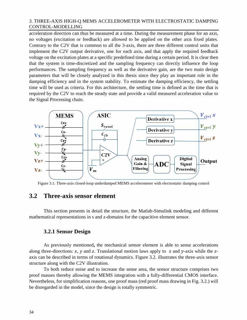
3. THREE-AXIS HIGH-Q MEMS ACCELEROMETER WITH ELECTROSTATIC DAMPING
CONTROL-MODELLING
34
acceleration direction can thus be measured at a time. During the measurement phase for an axis,
no voltages (excitation or feedback) are allowed to be applied on the other axis fixed plates.
Contrary to the C2V that is common to all the 3-axis, there are three different control units that
implement the C2V output derivative, one for each axis, and that apply the required feedback
voltage on the excitation plates at a specific predefined time during a certain period. It is clear then
that the system is time-discretized and the sampling frequency can directly influence the loop
performances. The sampling frequency as well as the derivative gain, are the two main design
parameters that will be closely analyzed in this thesis since they play an important role in the
damping efficiency and in the system stability. To estimate the damping efficiency, the settling
time will be used as criteria. For this architecture, the settling time is defined as the time that is
required by the C2V to reach the steady state and provide a valid measured acceleration value to
the Signal Processing chain.
Figure 3.1. Three-axis closed-loop underdamped MEMS accelerometer with electrostatic damping control
3.2 Three-axis sensor element
This section presents in detail the structure, the Matlab-Simulink modeling and different
mathematical representations in s and z-domains for the capacitive element sensor.
3.2.1 Sensor Design
As previously mentioned, the mechanical sensor element is able to sense accelerations
along three-directions: 𝑥, 𝑦 and 𝑧. Translational motion laws apply to 𝑥 and 𝑦-axis while the 𝑧-
axis can be described in terms of rotational dynamics. Figure 3.2. illustrates the three-axis sensor
structure along with the C2V illustration. To both reduce noise and to increase the sense area, the sensor structure comprises two
proof masses thereby allowing the MEMS integration with a fully-differential CMOS interface.
Nevertheless, for simplification reasons, one proof mass (red proof mass drawing in Fig. 3.2.) will
be disregarded in the model, since the design is totally symmetric.
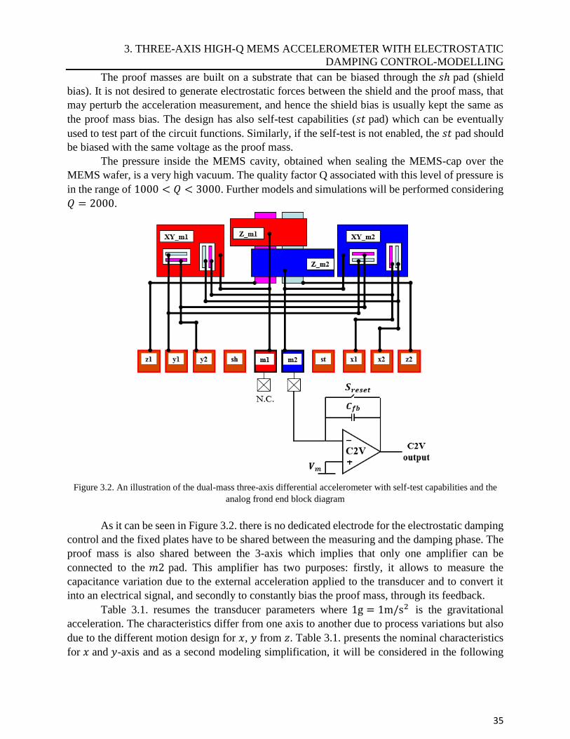
3. THREE-AXIS HIGH-Q MEMS ACCELEROMETER WITH ELECTROSTATIC
DAMPING CONTROL-MODELLING
35
The proof masses are built on a substrate that can be biased through the 𝑠ℎ pad (shield
bias). It is not desired to generate electrostatic forces between the shield and the proof mass, that
may perturb the acceleration measurement, and hence the shield bias is usually kept the same as
the proof mass bias. The design has also self-test capabilities (𝑠𝑡 pad) which can be eventually
used to test part of the circuit functions. Similarly, if the self-test is not enabled, the 𝑠𝑡 pad should
be biased with the same voltage as the proof mass. The pressure inside the MEMS cavity, obtained when sealing the MEMS-cap over the
MEMS wafer, is a very high vacuum. The quality factor Q associated with this level of pressure is
in the range of 1000 < 𝑄 < 3000. Further models and simulations will be performed considering
𝑄 = 2000.
Figure 3.2. An illustration of the dual-mass three-axis differential accelerometer with self-test capabilities and the
analog frond end block diagram
As it can be seen in Figure 3.2. there is no dedicated electrode for the electrostatic damping
control and the fixed plates have to be shared between the measuring and the damping phase. The
proof mass is also shared between the 3-axis which implies that only one amplifier can be
connected to the 𝑚2 pad. This amplifier has two purposes: firstly, it allows to measure the
capacitance variation due to the external acceleration applied to the transducer and to convert it
into an electrical signal, and secondly to constantly bias the proof mass, through its feedback.
Table 3.1. resumes the transducer parameters where 1g = 1m/s2 is the gravitational
acceleration. The characteristics differ from one axis to another due to process variations but also
due to the different motion design for 𝑥, 𝑦 from 𝑧. Table 3.1. presents the nominal characteristics
for 𝑥 and 𝑦-axis and as a second modeling simplification, it will be considered in the following
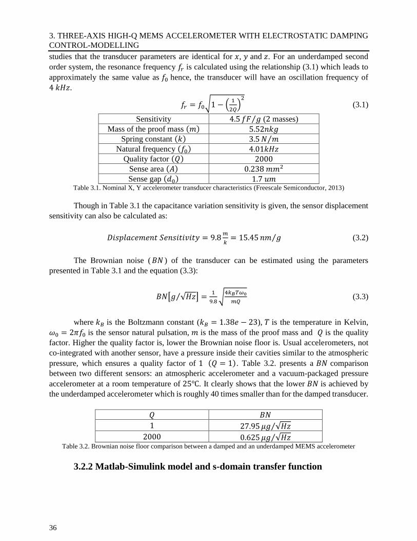
3. THREE-AXIS HIGH-Q MEMS ACCELEROMETER WITH ELECTROSTATIC DAMPING
CONTROL-MODELLING
36
studies that the transducer parameters are identical for 𝑥, 𝑦 and 𝑧. For an underdamped second
order system, the resonance frequency 𝑓𝑟 is calculated using the relationship (3.1) which leads to
approximately the same value as 𝑓0 hence, the transducer will have an oscillation frequency of
4 𝑘𝐻𝑧.
𝑓𝑟 = 𝑓0√1 − (1
2𝑄)
2
(3.1)
Sensitivity 4.5 𝑓𝐹 𝑔⁄ (2 masses)
Mass of the proof mass (𝑚) 5.52𝑛𝑘𝑔 Spring constant (𝑘) 3.5 𝑁 𝑚⁄
Natural frequency (𝑓0) 4.01𝑘𝐻𝑧
Quality factor (𝑄) 2000
Sense area (𝐴) 0.238 𝑚𝑚2
Sense gap (𝑑0) 1.7 𝑢𝑚 Table 3.1. Nominal X, Y accelerometer transducer characteristics (Freescale Semiconductor, 2013)
Though in Table 3.1 the capacitance variation sensitivity is given, the sensor displacement
sensitivity can also be calculated as:
𝐷𝑖𝑠𝑝𝑙𝑎𝑐𝑒𝑚𝑒𝑛𝑡 𝑆𝑒𝑛𝑠𝑖𝑡𝑖𝑣𝑖𝑡𝑦 = 9.8𝑚
𝑘= 15.45 𝑛𝑚 𝑔⁄ (3.2)
The Brownian noise ( 𝐵𝑁 ) of the transducer can be estimated using the parameters
presented in Table 3.1 and the equation (3.3):
𝐵𝑁[𝑔 √𝐻𝑧⁄ ] =1
9.8√
4𝑘𝐵𝑇𝜔0
𝑚𝑄 (3.3)
where 𝑘𝐵 is the Boltzmann constant (𝑘𝐵 = 1.38𝑒 − 23), 𝑇 is the temperature in Kelvin,
𝜔0 = 2𝜋𝑓0 is the sensor natural pulsation, 𝑚 is the mass of the proof mass and 𝑄 is the quality
factor. Higher the quality factor is, lower the Brownian noise floor is. Usual accelerometers, not
co-integrated with another sensor, have a pressure inside their cavities similar to the atmospheric
pressure, which ensures a quality factor of 1 (𝑄 = 1). Table 3.2. presents a 𝐵𝑁 comparison
between two different sensors: an atmospheric accelerometer and a vacuum-packaged pressure
accelerometer at a room temperature of 25. It clearly shows that the lower 𝐵𝑁 is achieved by
the underdamped accelerometer which is roughly 40 times smaller than for the damped transducer.
𝑄 𝐵𝑁
1 27.95 𝜇𝑔 √𝐻𝑧⁄
2000 0.625 𝜇𝑔 √𝐻𝑧⁄ Table 3.2. Brownian noise floor comparison between a damped and an underdamped MEMS accelerometer
3.2.2 Matlab-Simulink model and s-domain transfer function
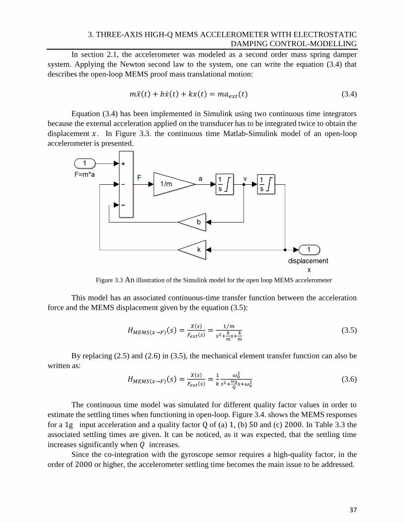
3. THREE-AXIS HIGH-Q MEMS ACCELEROMETER WITH ELECTROSTATIC
DAMPING CONTROL-MODELLING
37
In section 2.1, the accelerometer was modeled as a second order mass spring damper
system. Applying the Newton second law to the system, one can write the equation (3.4) that
describes the open-loop MEMS proof mass translational motion:
𝑚(𝑡) + 𝑏(𝑡) + 𝑘𝑥(𝑡) = 𝑚𝑎𝑒𝑥𝑡(𝑡) (3.4)
Equation (3.4) has been implemented in Simulink using two continuous time integrators
because the external acceleration applied on the transducer has to be integrated twice to obtain the
displacement 𝑥 . In Figure 3.3. the continuous time Matlab-Simulink model of an open-loop
accelerometer is presented.
Figure 3.3 An illustration of the Simulink model for the open loop MEMS accelerometer
This model has an associated continuous-time transfer function between the acceleration
force and the MEMS displacement given by the equation (3.5):
𝐻𝑀𝐸𝑀𝑆(𝑥→𝐹)(𝑠) =𝑋(𝑠)
𝐹𝑒𝑥𝑡(𝑠)=
1 𝑚⁄
𝑠2+𝑏
𝑚𝑠+
𝑘
𝑚
(3.5)
By replacing (2.5) and (2.6) in (3.5), the mechanical element transfer function can also be
written as:
𝐻𝑀𝐸𝑀𝑆(𝑥→𝐹)(𝑠) =𝑋(𝑠)
𝐹𝑒𝑥𝑡(𝑠)=
1
𝑘
𝜔02
𝑠2+𝜔0𝑄
𝑠+𝜔02 (3.6)
The continuous time model was simulated for different quality factor values in order to
estimate the settling times when functioning in open-loop. Figure 3.4. shows the MEMS responses
for a 1g input acceleration and a quality factor Q of (a) 1, (b) 50 and (c) 2000. In Table 3.3 the
associated settling times are given. It can be noticed, as it was expected, that the settling time
increases significantly when 𝑄 increases. Since the co-integration with the gyroscope sensor requires a high-quality factor, in the
order of 2000 or higher, the accelerometer settling time becomes the main issue to be addressed.
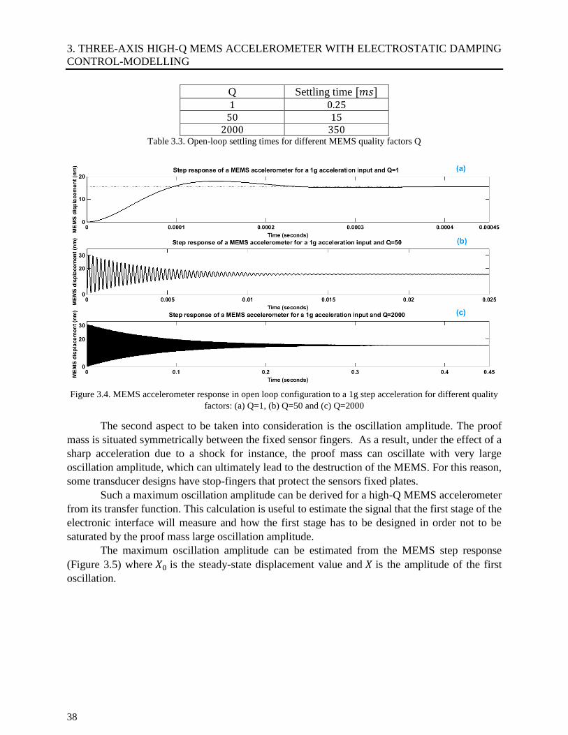
3. THREE-AXIS HIGH-Q MEMS ACCELEROMETER WITH ELECTROSTATIC DAMPING
CONTROL-MODELLING
38
Q Settling time [𝑚𝑠] 1 0.25
50 15 2000 350
Table 3.3. Open-loop settling times for different MEMS quality factors Q
Figure 3.4. MEMS accelerometer response in open loop configuration to a 1g step acceleration for different quality
factors: (a) Q=1, (b) Q=50 and (c) Q=2000
The second aspect to be taken into consideration is the oscillation amplitude. The proof
mass is situated symmetrically between the fixed sensor fingers. As a result, under the effect of a
sharp acceleration due to a shock for instance, the proof mass can oscillate with very large
oscillation amplitude, which can ultimately lead to the destruction of the MEMS. For this reason,
some transducer designs have stop-fingers that protect the sensors fixed plates. Such a maximum oscillation amplitude can be derived for a high-Q MEMS accelerometer
from its transfer function. This calculation is useful to estimate the signal that the first stage of the
electronic interface will measure and how the first stage has to be designed in order not to be
saturated by the proof mass large oscillation amplitude. The maximum oscillation amplitude can be estimated from the MEMS step response
(Figure 3.5) where 𝑋0 is the steady-state displacement value and 𝑋 is the amplitude of the first
oscillation.
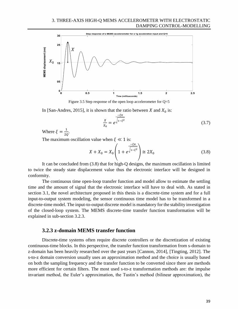
3. THREE-AXIS HIGH-Q MEMS ACCELEROMETER WITH ELECTROSTATIC
DAMPING CONTROL-MODELLING
39
Figure 3.5 Step response of the open loop accelerometer for Q=5
In [San-Andres, 2015], it is shown that the ratio between 𝑋 and 𝑋0 is:
𝑋
𝑋0= 𝑒
−𝜉𝜋
√1−𝜉2 (3.7)
Where 𝜉 =1
2𝑄.
The maximum oscillation value when 𝜉 ≪ 1 is:
𝑋 + 𝑋0 = 𝑋0 (1 + 𝑒
−𝜉𝜋
√1−𝜉2) ≅ 2𝑋0 (3.8)
It can be concluded from (3.8) that for high-Q designs, the maximum oscillation is limited
to twice the steady state displacement value thus the electronic interface will be designed in
conformity.
The continuous time open-loop transfer function and model allow to estimate the settling
time and the amount of signal that the electronic interface will have to deal with. As stated in
section 3.1, the novel architecture proposed in this thesis is a discrete-time system and for a full
input-to-output system modeling, the sensor continuous time model has to be transformed in a
discrete-time model. The input-to-output discrete model is mandatory for the stability investigation
of the closed-loop system. The MEMS discrete-time transfer function transformation will be
explained in sub-section 3.2.3.
3.2.3 z-domain MEMS transfer function
Discrete-time systems often require discrete controllers or the discretization of existing
continuous-time blocks. In this perspective, the transfer function transformation from s-domain to
z-domain has been heavily researched over the past years [Cannon, 2014], [Tingting, 2012]. The
s-to-z domain conversion usually uses an approximation method and the choice is usually based
on both the sampling frequency and the transfer function to be converted since there are methods
more efficient for certain filters. The most used s-to-z transformation methods are: the impulse
invariant method, the Euler’s approximation, the Tustin’s method (bilinear approximation), the
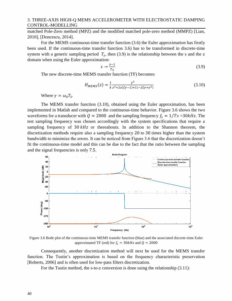
3. THREE-AXIS HIGH-Q MEMS ACCELEROMETER WITH ELECTROSTATIC DAMPING
CONTROL-MODELLING
40
matched Pole-Zero method (MPZ) and the modified matched pole-zero method (MMPZ) [Lian,
2010], [Doncescu, 2014]. For the MEMS continuous-time transfer function (3.6) the Euler approximation has firstly
been used. If the continuous-time transfer function 3.6) has to be transformed in discrete-time
system with a generic sampling period 𝑇𝑠, then (3.9) is the relationship between the s and the z
domain when using the Euler approximation:
𝑠 →𝑧−1
𝑇𝑆 (3.9)
The new discrete-time MEMS transfer function (TF) becomes:
𝐻𝑀𝐸𝑀𝑆(𝑧) =1
𝑘
𝛾2
𝑧2+2𝑧(𝜉𝛾−1)+(1−2𝜉𝛾+𝛾2) (3.10)
Where 𝛾 = 𝜔0𝑇𝑆.
The MEMS transfer function (3.10), obtained using the Euler approximation, has been
implemented in Matlab and compared to the continuous-time behavior. Figure 3.6 shows the two
waveforms for a transducer with 𝑄 = 2000 and the sampling frequency 𝑓𝑠 = 1 𝑇𝑠⁄ =30𝑘𝐻𝑧. The
test sampling frequency was chosen accordingly with the system specifications that require a
sampling frequency of 30 𝑘𝐻𝑧 or thereabouts. In addition to the Shannon theorem, the
discretization methods require also a sampling frequency 20 to 30 times higher than the system
bandwidth to minimize the errors. It can be noticed from Figure 3.6 that the discretization doesn’t
fit the continuous-time model and this can be due to the fact that the ratio between the sampling
and the signal frequencies is only 7.5.
Figure 3.6 Bode plot of the continuous-time MEMS transfer function (blue) and the associated discrete-time Euler
approximated TF (red) for 𝑓𝑠 = 30𝑘𝐻𝑧 and 𝑄 = 2000
Consequently, another discretization method will next be used for the MEMS transfer
function. The Tustin’s approximation is based on the frequency characteristic preservation
[Roberts, 2006] and is often used for low-pass filters discretization.
For the Tustin method, the s-to-z conversion is done using the relationship (3.11):
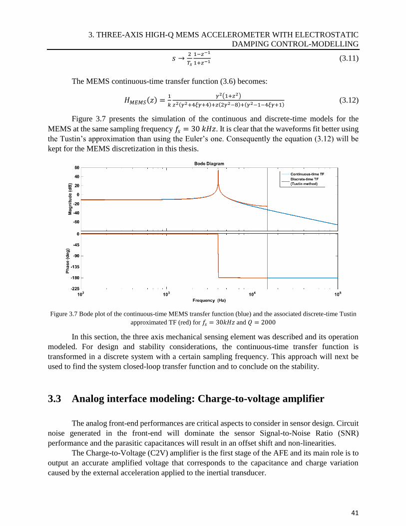
3. THREE-AXIS HIGH-Q MEMS ACCELEROMETER WITH ELECTROSTATIC
DAMPING CONTROL-MODELLING
41
𝑠 →2
𝑇𝑠
1−𝑧−1
1+𝑧−1 (3.11)
The MEMS continuous-time transfer function (3.6) becomes:
𝐻𝑀𝐸𝑀𝑆(𝑧) =1
𝑘
𝛾2(1+𝑧2)
𝑧2(𝛾2+4𝜉𝛾+4)+𝑧(2𝛾2−8)+(𝛾2−1−4𝜉𝛾+1) (3.12)
Figure 3.7 presents the simulation of the continuous and discrete-time models for the
MEMS at the same sampling frequency 𝑓𝑠 = 30 𝑘𝐻𝑧. It is clear that the waveforms fit better using
the Tustin’s approximation than using the Euler’s one. Consequently the equation (3.12) will be
kept for the MEMS discretization in this thesis.
Figure 3.7 Bode plot of the continuous-time MEMS transfer function (blue) and the associated discrete-time Tustin
approximated TF (red) for 𝑓𝑠 = 30𝑘𝐻𝑧 and 𝑄 = 2000
In this section, the three axis mechanical sensing element was described and its operation
modeled. For design and stability considerations, the continuous-time transfer function is
transformed in a discrete system with a certain sampling frequency. This approach will next be
used to find the system closed-loop transfer function and to conclude on the stability.
3.3 Analog interface modeling: Charge-to-voltage amplifier
The analog front-end performances are critical aspects to consider in sensor design. Circuit
noise generated in the front-end will dominate the sensor Signal-to-Noise Ratio (SNR)
performance and the parasitic capacitances will result in an offset shift and non-linearities.
The Charge-to-Voltage (C2V) amplifier is the first stage of the AFE and its main role is to
output an accurate amplified voltage that corresponds to the capacitance and charge variation
caused by the external acceleration applied to the inertial transducer.
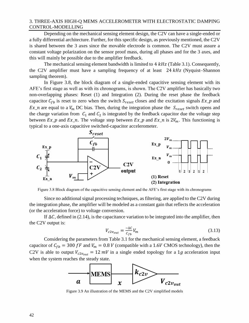
3. THREE-AXIS HIGH-Q MEMS ACCELEROMETER WITH ELECTROSTATIC DAMPING
CONTROL-MODELLING
42
Depending on the mechanical sensing element design, the C2V can have a single-ended or
a fully differential architecture. Further, for this specific design, as previously mentioned, the C2V
is shared between the 3 axes since the movable electrode is common. The C2V must assure a
constant voltage polarization on the sensor proof mass, during all phases and for the 3 axes, and
this will mainly be possible due to the amplifier feedback.
The mechanical sensing element bandwidth is limited to 4 𝑘𝐻𝑧 (Table 3.1). Consequently,
the C2V amplifier must have a sampling frequency of at least 24 𝑘𝐻𝑧 (Nyquist–Shannon
sampling theorem). In Figure 3.8, the block diagram of a single-ended capacitive sensing element with its
AFE’s first stage as well as with its chronograms, is shown. The C2V amplifier has basically two
non-overlapping phases: Reset (1) and Integration (2). During the reset phase the feedback
capacitor 𝐶𝑓𝑏 is reset to zero when the switch 𝑆𝑟𝑒𝑠𝑒𝑡 closes and the excitation signals 𝐸𝑥_𝑝 and
𝐸𝑥_𝑛 are equal to a 𝑉𝑚 DC bias. Then, during the integration phase the 𝑆𝑟𝑒𝑠𝑒𝑡 switch opens and
the charge variation from 𝐶1 and 𝐶2 is integrated by the feedback capacitor due the voltage step
between 𝐸𝑥_𝑝 and 𝐸𝑥_𝑛. The voltage step between 𝐸𝑥_𝑝 and 𝐸𝑥_𝑛 is 2𝑉𝑚. This functioning is
typical to a one-axis capacitive switched-capacitor accelerometer.
Figure 3.8 Block diagram of the capacitive sensing element and the AFE’s first stage with its chronograms
Since no additional signal processing techniques, as filtering, are applied to the C2V during
the integration phase, the amplifier will be modeled as a constant gain that reflects the acceleration
(or the acceleration force) to voltage conversion.
If ∆𝐶, defined in (2.14), is the capacitance variation to be integrated into the amplifier, then
the C2V output is:
𝑉𝑐2𝑣𝑜𝑢𝑡=
−∆𝐶
𝐶𝑓𝑏𝑉𝑚 (3.13)
Considering the parameters from Table 3.1 for the mechanical sensing element, a feedback
capacitor of 𝐶𝑓𝑏 = 300 𝑓𝐹 and 𝑉𝑚 = 0.8 𝑉 (compatible with a 1.6𝑉 CMOS technology), then the
C2V is able to output 𝑉𝑐2𝑣𝑜𝑢𝑡= 12 𝑚𝑉 in a single ended topology for a 1𝑔 acceleration input
when the system reaches the steady state.
Figure 3.9 An illustration of the MEMS and the C2V simplified models
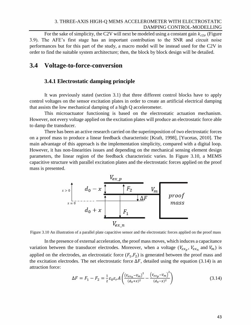
3. THREE-AXIS HIGH-Q MEMS ACCELEROMETER WITH ELECTROSTATIC
DAMPING CONTROL-MODELLING
43
For the sake of simplicity, the C2V will next be modeled using a constant gain 𝑘𝑐2𝑣 (Figure
3.9). The AFE’s first stage has an important contribution to the SNR and circuit noise
performances but for this part of the study, a macro model will be instead used for the C2V in
order to find the suitable system architecture; then, the block by block design will be detailed.
3.4 Voltage-to-force-conversion
3.4.1 Electrostatic damping principle
It was previously stated (section 3.1) that three different control blocks have to apply
control voltages on the sensor excitation plates in order to create an artificial electrical damping
that assists the low mechanical damping of a high Q accelerometer.
This microactuator functioning is based on the electrostatic actuation mechanism.
However, not every voltage applied on the excitation plates will produce an electrostatic force able
to damp the transducer.
There has been an active research carried on the superimposition of two electrostatic forces
on a proof mass to produce a linear feedback characteristic [Kraft, 1998], [Yucetas, 2010]. The
main advantage of this approach is the implementation simplicity, compared with a digital loop.
However, it has non-linearities issues and depending on the mechanical sensing element design
parameters, the linear region of the feedback characteristic varies. In Figure 3.10, a MEMS
capacitive structure with parallel excitation plates and the electrostatic forces applied on the proof
mass is presented.
Figure 3.10 An illustration of a parallel plate capacitive sensor and the electrostatic forces applied on the proof mass
In the presence of external acceleration, the proof mass moves, which induces a capacitance
variation between the transducer electrodes. Moreover, when a voltage (𝑉𝑒𝑥𝑝, 𝑉𝑒𝑥𝑛
and 𝑉𝑚) is
applied on the electrodes, an electrostatic force (𝐹1,𝐹2) is generated between the proof mass and
the excitation electrodes. The net electrostatic force ∆𝐹, detailed using the equation (3.14) is an
attraction force:
∆𝐹 = 𝐹1 − 𝐹2 =1
2𝜀0𝜀𝑟𝐴 (
(𝑉𝑒𝑥𝑛−𝑉𝑚)2
(𝑑0+𝑥)2−
(𝑉𝑒𝑥𝑝−𝑉𝑚)2
(𝑑0−𝑥)2) (3.14)
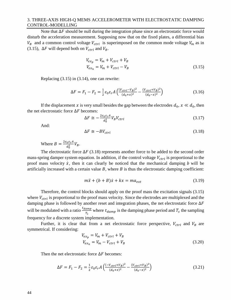
3. THREE-AXIS HIGH-Q MEMS ACCELEROMETER WITH ELECTROSTATIC DAMPING
CONTROL-MODELLING
44
Note that ∆𝐹 should be null during the integration phase since an electrostatic force would
disturb the acceleration measurement. Supposing now that on the fixed plates, a differential bias
𝑉𝐵 and a common control voltage 𝑉𝑐𝑡𝑟𝑙 is superimposed on the common mode voltage 𝑉𝑚 as in
(3.15), ∆𝐹 will depend both on 𝑉𝑐𝑡𝑟𝑙 and 𝑉𝐵.
𝑉𝑒𝑥𝑝= 𝑉𝑚 + 𝑉𝑐𝑡𝑟𝑙 + 𝑉𝐵
𝑉𝑒𝑥𝑛= 𝑉𝑚 + 𝑉𝑐𝑡𝑟𝑙 − 𝑉𝐵 (3.15)
Replacing (3.15) in (3.14), one can rewrite:
∆𝐹 = 𝐹1 − 𝐹2 =1
2𝜀0𝜀𝑟𝐴 (
(𝑉𝑐𝑡𝑟𝑙−𝑉𝐵)2
(𝑑0+𝑥)2 −(𝑉𝑐𝑡𝑟𝑙+𝑉𝐵)2
(𝑑0−𝑥)2 ) (3.16)
If the displacement 𝑥 is very small besides the gap between the electrodes 𝑑0, 𝑥 ≪ 𝑑0, then
the net electrostatic force ∆𝐹 becomes:
∆𝐹 ≅ −2𝜀0𝜀𝑟𝐴
𝑑02 𝑉𝐵𝑉𝑐𝑡𝑟𝑙 (3.17)
And:
∆𝐹 ≅ −𝐵𝑉𝑐𝑡𝑟𝑙 (3.18)
Where 𝐵 =2𝜀0𝜀𝑟𝐴
𝑑02 𝑉𝐵.
The electrostatic force ∆𝐹 (3.18) represents another force to be added to the second order
mass-spring damper system equation. In addition, if the control voltage 𝑉𝑐𝑡𝑟𝑙 is proportional to the
proof mass velocity , then it can clearly be noticed that the mechanical damping 𝑏 will be
artificially increased with a certain value 𝐵, where 𝐵 is thus the electrostatic damping coefficient:
𝑚 + (𝑏 + 𝐵) + 𝑘𝑥 = 𝑚𝑎𝑒𝑥𝑡 (3.19)
Therefore, the control blocks should apply on the proof mass the excitation signals (3.15)
where 𝑉𝑐𝑡𝑟𝑙 is proportional to the proof mass velocity. Since the electrodes are multiplexed and the
damping phase is followed by another reset and integration phases, the net electrostatic force ∆𝐹
will be modulated with a ratio 𝑡𝑑𝑎𝑚𝑝
𝑇𝑠 where 𝑡𝑑𝑎𝑚𝑝 is the damping phase period and 𝑇𝑠 the sampling
frequency for a discrete system implementation.
Further, it is clear that from a net electrostatic force perspective, 𝑉𝑐𝑡𝑟𝑙 and 𝑉𝐵 are
symmetrical. If considering:
𝑉𝑒𝑥𝑝= 𝑉𝑚 + 𝑉𝑐𝑡𝑟𝑙 + 𝑉𝐵
𝑉𝑒𝑥𝑛= 𝑉𝑚 − 𝑉𝑐𝑡𝑟𝑙 + 𝑉𝐵 (3.20)
Then the net electrostatic force ∆𝐹 becomes:
∆𝐹 = 𝐹1 − 𝐹2 =1
2𝜀0𝜀𝑟𝐴 (
(−𝑉𝑐𝑡𝑟𝑙+𝑉𝐵)2
(𝑑0+𝑥)2 −(𝑉𝑐𝑡𝑟𝑙+𝑉𝐵)2
(𝑑0−𝑥)2 ) (3.21)
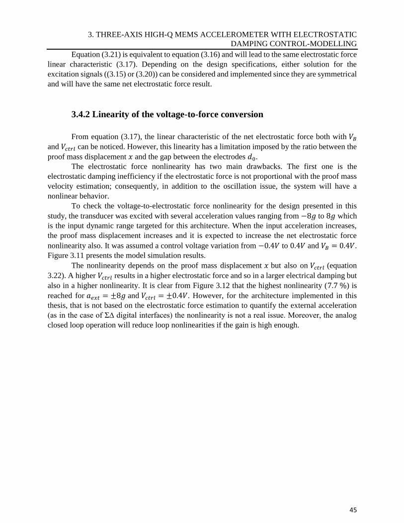
3. THREE-AXIS HIGH-Q MEMS ACCELEROMETER WITH ELECTROSTATIC
DAMPING CONTROL-MODELLING
45
Equation (3.21) is equivalent to equation (3.16) and will lead to the same electrostatic force
linear characteristic (3.17). Depending on the design specifications, either solution for the
excitation signals ((3.15) or (3.20)) can be considered and implemented since they are symmetrical
and will have the same net electrostatic force result.
3.4.2 Linearity of the voltage-to-force conversion
From equation (3.17), the linear characteristic of the net electrostatic force both with 𝑉𝐵
and 𝑉𝑐𝑡𝑟𝑙 can be noticed. However, this linearity has a limitation imposed by the ratio between the
proof mass displacement 𝑥 and the gap between the electrodes 𝑑0. The electrostatic force nonlinearity has two main drawbacks. The first one is the
electrostatic damping inefficiency if the electrostatic force is not proportional with the proof mass
velocity estimation; consequently, in addition to the oscillation issue, the system will have a
nonlinear behavior. To check the voltage-to-electrostatic force nonlinearity for the design presented in this
study, the transducer was excited with several acceleration values ranging from −8𝑔 to 8𝑔 which
is the input dynamic range targeted for this architecture. When the input acceleration increases,
the proof mass displacement increases and it is expected to increase the net electrostatic force
nonlinearity also. It was assumed a control voltage variation from −0.4𝑉 to 0.4𝑉 and 𝑉𝐵 = 0.4𝑉.
Figure 3.11 presents the model simulation results.
The nonlinearity depends on the proof mass displacement 𝑥 but also on 𝑉𝑐𝑡𝑟𝑙 (equation
3.22). A higher 𝑉𝑐𝑡𝑟𝑙 results in a higher electrostatic force and so in a larger electrical damping but
also in a higher nonlinearity. It is clear from Figure 3.12 that the highest nonlinearity (7.7 %) is
reached for 𝑎𝑒𝑥𝑡 = ±8𝑔 and 𝑉𝑐𝑡𝑟𝑙 = ±0.4𝑉. However, for the architecture implemented in this
thesis, that is not based on the electrostatic force estimation to quantify the external acceleration
(as in the case of Σ∆ digital interfaces) the nonlinearity is not a real issue. Moreover, the analog
closed loop operation will reduce loop nonlinearities if the gain is high enough.
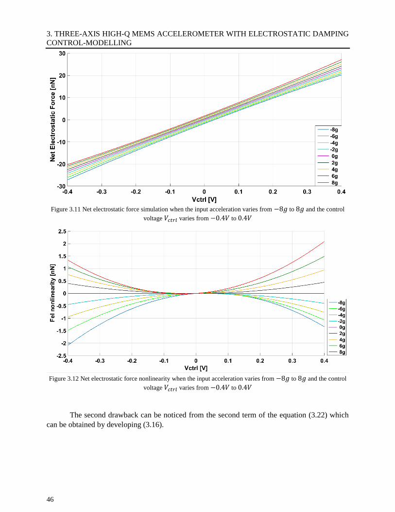
3. THREE-AXIS HIGH-Q MEMS ACCELEROMETER WITH ELECTROSTATIC DAMPING
CONTROL-MODELLING
46
Figure 3.11 Net electrostatic force simulation when the input acceleration varies from −8𝑔 to 8𝑔 and the control
voltage 𝑉𝑐𝑡𝑟𝑙 varies from −0.4𝑉 to 0.4𝑉
Figure 3.12 Net electrostatic force nonlinearity when the input acceleration varies from −8𝑔 to 8𝑔 and the control
voltage 𝑉𝑐𝑡𝑟𝑙 varies from −0.4𝑉 to 0.4𝑉
The second drawback can be noticed from the second term of the equation (3.22) which
can be obtained by developing (3.16).
3. THREE-AXIS HIGH-Q MEMS ACCELEROMETER WITH ELECTROSTATIC
DAMPING CONTROL-MODELLING
47
∆𝐹 =−2𝜀0𝜀𝑟𝐴
𝑑02 𝑉𝑐𝑡𝑟𝑙𝑉𝐵
1+(𝑥
𝑑0)
2
(1−(𝑥
𝑑0)
2)
2 −𝜀0𝜀𝑟𝐴
𝑑02
𝑥
𝑑0(𝑉𝑐𝑡𝑟𝑙
2 + 𝑉𝐵2)
1
(1−(𝑥
𝑑0)
2)
2 (3.22)
It consists in adding a displacement-proportional term 𝑘′ in the second order mass spring
damper equation (3.23) that will cause a change in the sensor resonance frequency (𝑓𝑟𝑒𝑠). Since it
is desired to modify only the proof mass velocity, the resonance frequency shift (3.24) can be
considered a drawback.
𝑚 + (𝑏 + 𝐵) + (𝑘 + 𝑘′)𝑥 = 𝑚𝑎𝑒𝑥𝑡 (3.23)
𝑓𝑟𝑒𝑠 =1
2𝜋√
𝑘+𝑘′
𝑚 (3.24)
Increasing the DC voltage 𝑉𝐵 and 𝑉𝑐𝑡𝑟𝑙 will increase also the nonlinearity coefficient 𝑘′. In
the same time, the net electrostatic force can be maximized by choosing the optimum value for 𝑉𝐵.
The 𝑉𝐵 calculation for a maximum net electrostatic force generation will be next presented.
3.4.3 Bias calculation for electrostatic force optimization
In order to find the design parameter 𝑉𝐵, several design assumptions have to be made. The
first one is the targeted CMOS process: the accelerometer architecture should be designed in a
0.18 µ𝑚 CMOS technology within a 𝑉𝑑𝑑 = 1.6𝑉 power supply. Secondly, no additional charge
pump circuit can be used since the CMOS technology is not high-voltage compatible and the
system has to be low power and small area. Then, no negative voltage can be generated or applied
with the IC. Finally, it was chosen to have a common mode voltage of 𝑉𝑚 = 0.8𝑉 to maximize
the dynamic range. In this conditions, equations (3.15) can be rewritten as:
𝑉𝑒𝑥𝑝= 0.8 + 𝑉𝑐𝑡𝑟𝑙 + 𝑉𝐵
𝑉𝑒𝑥𝑛= 0.8 + 𝑉𝑐𝑡𝑟𝑙 − 𝑉𝐵 (3.25)
In addition, the positive excitation signal 𝑉𝑒𝑥𝑝 can reach 𝑉𝑑𝑑 at most and 𝑉𝑒𝑥𝑛
can’t be
lower than the analog ground 0𝑉.
(𝑉𝑐𝑡𝑟𝑙 + 𝑉𝐵)𝑚𝑎𝑥 = 𝑉𝑚
(𝑉𝑐𝑡𝑟𝑙 − 𝑉𝐵)𝑚𝑖𝑛 = −𝑉𝑚 (3.26)
Depending on 𝑉𝐵, we can now define a maximum and a minimum for the net electrostatic
force approximation:
∆𝐹𝑚𝑎𝑥 ≅2𝜀0𝜀𝑟𝐴
𝑑02 ×( 𝑉𝐵× 𝑉𝑐𝑡𝑟𝑙)𝑚𝑎𝑥 =
2𝜀0𝜀𝑟𝐴
𝑑02 × 𝑉𝐵× (𝑉𝑐𝑡𝑟𝑙)𝑚𝑎𝑥 = 𝑓1(𝑉𝐵)
∆𝐹𝑚𝑖𝑛 ≅2𝜀0𝜀𝑟𝐴
𝑑02 ×( 𝑉𝐵× 𝑉𝑐𝑡𝑟𝑙)𝑚𝑖𝑛 =
2𝜀0𝜀𝑟𝐴
𝑑02 × 𝑉𝐵 ×(𝑉𝑐𝑡𝑟𝑙)𝑚𝑖𝑛 = 𝑓2(𝑉𝐵) (3.27)
If replacing (𝑉𝑐𝑡𝑟𝑙)𝑚𝑎𝑥 and (𝑉𝑐𝑡𝑟𝑙)𝑚𝑖𝑛 from (3.26) in (3.27) and imposing the annulation
of the first order derivative for 𝑓1 and 𝑓2 (
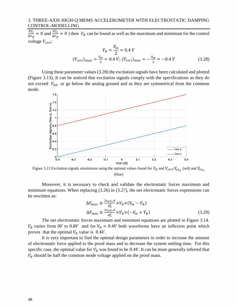
3. THREE-AXIS HIGH-Q MEMS ACCELEROMETER WITH ELECTROSTATIC DAMPING
CONTROL-MODELLING
48
𝜕𝑓1
𝜕𝑉𝐵= 0 and
𝜕𝑓2
𝜕𝑉𝐵= 0 ) then 𝑉𝐵 can be found as well as the maximum and minimum for the control
voltage 𝑉𝑐𝑡𝑟𝑙:
𝑉𝐵 =𝑉𝑚
2= 0.4 𝑉
(𝑉𝑐𝑡𝑟𝑙)𝑚𝑎𝑥 =𝑉𝑚
2= 0.4 𝑉; (𝑉𝑐𝑡𝑟𝑙)𝑚𝑖𝑛 = −
𝑉𝑚
2= −0.4 𝑉 (3.28)
Using these parameter values (3.28) the excitation signals have been calculated and plotted
(Figure 3.13). It can be noticed that excitation signals comply with the specifications as they do
not exceed 𝑉𝑑𝑑 or go below the analog ground and as they are symmetrical from the common
mode.
Figure 3.13 Excitation signals simulations using the optimal values found for 𝑉𝐵 and 𝑉𝑐𝑡𝑟𝑙:𝑉𝑒𝑥𝑝
(red) and 𝑉𝑒𝑥𝑛
(blue)
Moreover, it is necessary to check and validate the electrostatic forces maximum and
minimum equations. When replacing (3.26) in (3.27), the net electrostatic forces expressions can
be rewritten as:
∆𝐹𝑚𝑎𝑥 ≅2𝜀0𝜀𝑟𝐴
𝑑02 ×𝑉𝐵×(𝑉𝑚 − 𝑉𝐵)
∆𝐹𝑚𝑖𝑛 ≅2𝜀0𝜀𝑟𝐴
𝑑02 ×𝑉𝐵×(−𝑉𝑚 + 𝑉𝐵) (3.29)
The net electrostatic forces maximum and minimum equations are plotted in Figure 3.14.
𝑉𝐵 varies from 0𝑉 to 0.8𝑉 and for 𝑉𝐵 = 0.4𝑉 both waveforms have an inflexion point which
proves that the optimal 𝑉𝐵 value is 0.4𝑉. It is very important to find the optimal design parameters in order to increase the amount
of electrostatic force applied to the proof mass and to decrease the system settling time. For this
specific case, the optimal value for 𝑉𝐵 was found to be 0.4𝑉. It can be more generally inferred that
𝑉𝐵 should be half the common mode voltage applied on the proof mass.
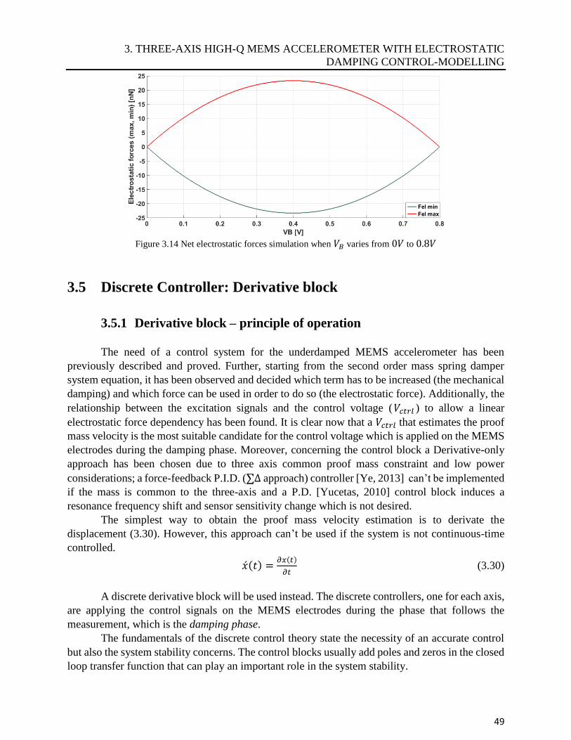
3. THREE-AXIS HIGH-Q MEMS ACCELEROMETER WITH ELECTROSTATIC
DAMPING CONTROL-MODELLING
49
Figure 3.14 Net electrostatic forces simulation when 𝑉𝐵 varies from 0𝑉 to 0.8𝑉
3.5 Discrete Controller: Derivative block
3.5.1 Derivative block – principle of operation
The need of a control system for the underdamped MEMS accelerometer has been
previously described and proved. Further, starting from the second order mass spring damper
system equation, it has been observed and decided which term has to be increased (the mechanical
damping) and which force can be used in order to do so (the electrostatic force). Additionally, the
relationship between the excitation signals and the control voltage (𝑉𝑐𝑡𝑟𝑙 ) to allow a linear
electrostatic force dependency has been found. It is clear now that a 𝑉𝑐𝑡𝑟𝑙 that estimates the proof
mass velocity is the most suitable candidate for the control voltage which is applied on the MEMS
electrodes during the damping phase. Moreover, concerning the control block a Derivative-only
approach has been chosen due to three axis common proof mass constraint and low power
considerations; a force-feedback P.I.D. (∑∆ approach) controller [Ye, 2013] can’t be implemented
if the mass is common to the three-axis and a P.D. [Yucetas, 2010] control block induces a
resonance frequency shift and sensor sensitivity change which is not desired. The simplest way to obtain the proof mass velocity estimation is to derivate the
displacement (3.30). However, this approach can’t be used if the system is not continuous-time
controlled.
(𝑡) =𝜕𝑥(𝑡)
𝜕𝑡 (3.30)
A discrete derivative block will be used instead. The discrete controllers, one for each axis,
are applying the control signals on the MEMS electrodes during the phase that follows the
measurement, which is the damping phase. The fundamentals of the discrete control theory state the necessity of an accurate control
but also the system stability concerns. The control blocks usually add poles and zeros in the closed
loop transfer function that can play an important role in the system stability.
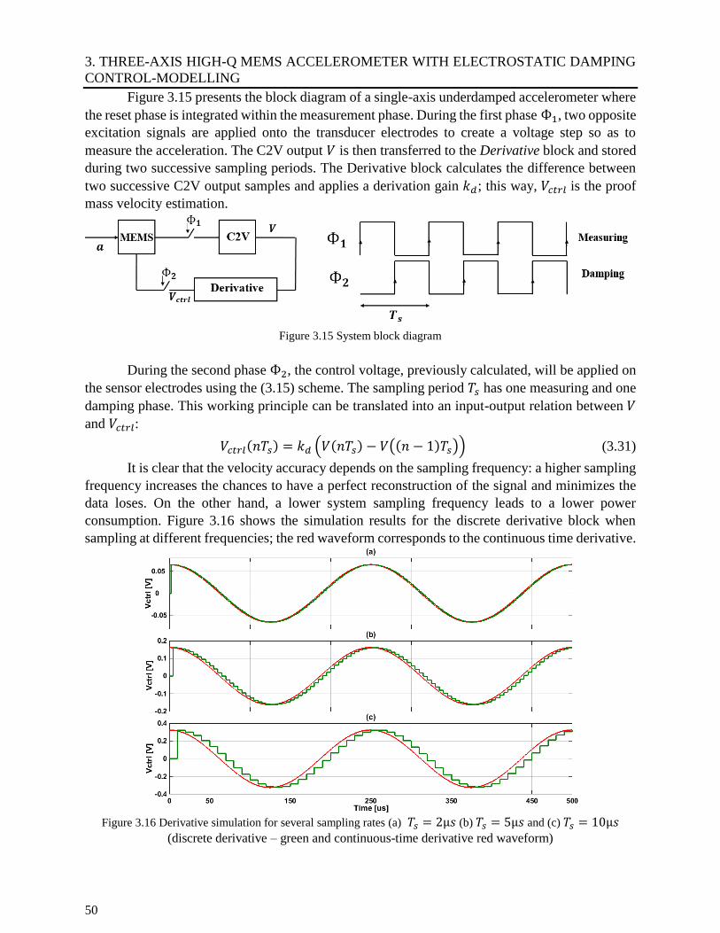
3. THREE-AXIS HIGH-Q MEMS ACCELEROMETER WITH ELECTROSTATIC DAMPING
CONTROL-MODELLING
50
Figure 3.15 presents the block diagram of a single-axis underdamped accelerometer where
the reset phase is integrated within the measurement phase. During the first phase Ф1, two opposite
excitation signals are applied onto the transducer electrodes to create a voltage step so as to
measure the acceleration. The C2V output 𝑉 is then transferred to the Derivative block and stored
during two successive sampling periods. The Derivative block calculates the difference between
two successive C2V output samples and applies a derivation gain 𝑘𝑑; this way, 𝑉𝑐𝑡𝑟𝑙 is the proof
mass velocity estimation.
Figure 3.15 System block diagram
During the second phase Ф2, the control voltage, previously calculated, will be applied on
the sensor electrodes using the (3.15) scheme. The sampling period 𝑇𝑠 has one measuring and one
damping phase. This working principle can be translated into an input-output relation between 𝑉
and 𝑉𝑐𝑡𝑟𝑙:
𝑉𝑐𝑡𝑟𝑙(𝑛𝑇𝑠) = 𝑘𝑑 (𝑉(𝑛𝑇𝑠) − 𝑉((𝑛 − 1)𝑇𝑠)) (3.31)
It is clear that the velocity accuracy depends on the sampling frequency: a higher sampling
frequency increases the chances to have a perfect reconstruction of the signal and minimizes the
data loses. On the other hand, a lower system sampling frequency leads to a lower power
consumption. Figure 3.16 shows the simulation results for the discrete derivative block when
sampling at different frequencies; the red waveform corresponds to the continuous time derivative.
Figure 3.16 Derivative simulation for several sampling rates (a) 𝑇𝑠 = 2µ𝑠 (b) 𝑇𝑠 = 5µ𝑠 and (c) 𝑇𝑠 = 10µ𝑠
(discrete derivative – green and continuous-time derivative red waveform)
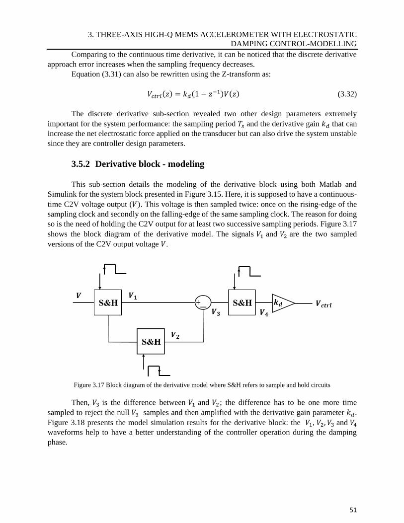
3. THREE-AXIS HIGH-Q MEMS ACCELEROMETER WITH ELECTROSTATIC
DAMPING CONTROL-MODELLING
51
Comparing to the continuous time derivative, it can be noticed that the discrete derivative
approach error increases when the sampling frequency decreases. Equation (3.31) can also be rewritten using the Z-transform as:
𝑉𝑐𝑡𝑟𝑙(𝑧) = 𝑘𝑑(1 − 𝑧−1)𝑉(𝑧) (3.32)
The discrete derivative sub-section revealed two other design parameters extremely
important for the system performance: the sampling period 𝑇𝑠 and the derivative gain 𝑘𝑑 that can
increase the net electrostatic force applied on the transducer but can also drive the system unstable
since they are controller design parameters.
3.5.2 Derivative block - modeling
This sub-section details the modeling of the derivative block using both Matlab and
Simulink for the system block presented in Figure 3.15. Here, it is supposed to have a continuous-
time C2V voltage output (𝑉). This voltage is then sampled twice: once on the rising-edge of the
sampling clock and secondly on the falling-edge of the same sampling clock. The reason for doing
so is the need of holding the C2V output for at least two successive sampling periods. Figure 3.17
shows the block diagram of the derivative model. The signals 𝑉1 and 𝑉2 are the two sampled
versions of the C2V output voltage 𝑉.
Figure 3.17 Block diagram of the derivative model where S&H refers to sample and hold circuits
Then, 𝑉3 is the difference between 𝑉1 and 𝑉2 ; the difference has to be one more time
sampled to reject the null 𝑉3 samples and then amplified with the derivative gain parameter 𝑘𝑑.
Figure 3.18 presents the model simulation results for the derivative block: the 𝑉1, 𝑉2, 𝑉3 and 𝑉4
waveforms help to have a better understanding of the controller operation during the damping
phase.
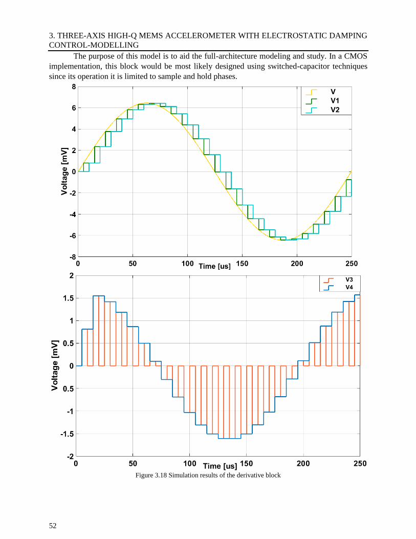
3. THREE-AXIS HIGH-Q MEMS ACCELEROMETER WITH ELECTROSTATIC DAMPING
CONTROL-MODELLING
52
The purpose of this model is to aid the full-architecture modeling and study. In a CMOS
implementation, this block would be most likely designed using switched-capacitor techniques
since its operation it is limited to sample and hold phases.
Figure 3.18 Simulation results of the derivative block
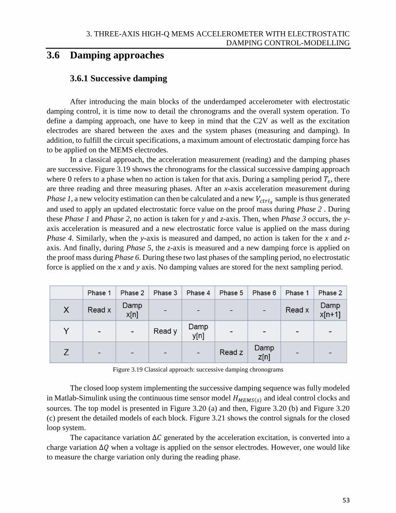
3. THREE-AXIS HIGH-Q MEMS ACCELEROMETER WITH ELECTROSTATIC
DAMPING CONTROL-MODELLING
53
3.6 Damping approaches
3.6.1 Successive damping
After introducing the main blocks of the underdamped accelerometer with electrostatic
damping control, it is time now to detail the chronograms and the overall system operation. To
define a damping approach, one have to keep in mind that the C2V as well as the excitation
electrodes are shared between the axes and the system phases (measuring and damping). In
addition, to fulfill the circuit specifications, a maximum amount of electrostatic damping force has
to be applied on the MEMS electrodes. In a classical approach, the acceleration measurement (reading) and the damping phases
are successive. Figure 3.19 shows the chronograms for the classical successive damping approach
where 0 refers to a phase when no action is taken for that axis. During a sampling period 𝑇𝑠, there
are three reading and three measuring phases. After an x-axis acceleration measurement during
Phase 1, a new velocity estimation can then be calculated and a new 𝑉𝑐𝑡𝑟𝑙𝑥 sample is thus generated
and used to apply an updated electrostatic force value on the proof mass during Phase 2 . During
these Phase 1 and Phase 2, no action is taken for y and z-axis. Then, when Phase 3 occurs, the y-
axis acceleration is measured and a new electrostatic force value is applied on the mass during
Phase 4. Similarly, when the y-axis is measured and damped, no action is taken for the x and z-
axis. And finally, during Phase 5, the z-axis is measured and a new damping force is applied on
the proof mass during Phase 6. During these two last phases of the sampling period, no electrostatic
force is applied on the x and y axis. No damping values are stored for the next sampling period.
Figure 3.19 Classical approach: successive damping chronograms
The closed loop system implementing the successive damping sequence was fully modeled
in Matlab-Simulink using the continuous time sensor model 𝐻𝑀𝐸𝑀𝑆(𝑠) and ideal control clocks and
sources. The top model is presented in Figure 3.20 (a) and then, Figure 3.20 (b) and Figure 3.20
(c) present the detailed models of each block. Figure 3.21 shows the control signals for the closed
loop system.
The capacitance variation ∆𝐶 generated by the acceleration excitation, is converted into a
charge variation ∆𝑄 when a voltage is applied on the sensor electrodes. However, one would like
to measure the charge variation only during the reading phase.
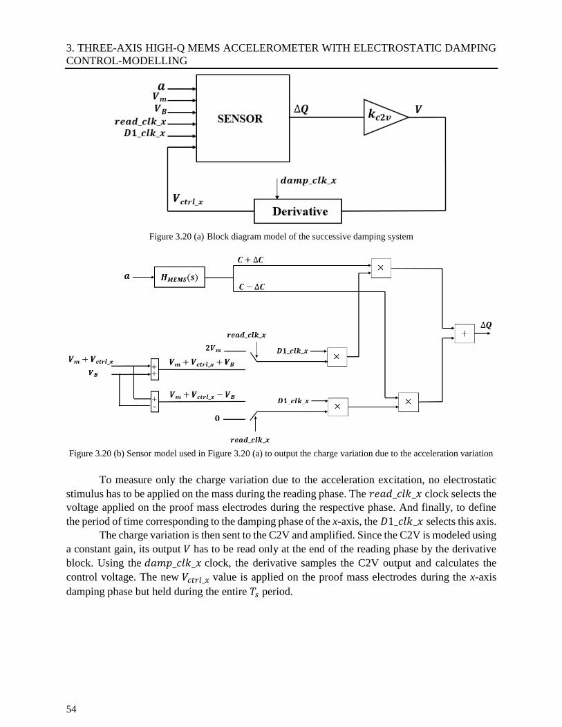
3. THREE-AXIS HIGH-Q MEMS ACCELEROMETER WITH ELECTROSTATIC DAMPING
CONTROL-MODELLING
54
Figure 3.20 (a) Block diagram model of the successive damping system
Figure 3.20 (b) Sensor model used in Figure 3.20 (a) to output the charge variation due to the acceleration variation
To measure only the charge variation due to the acceleration excitation, no electrostatic
stimulus has to be applied on the mass during the reading phase. The 𝑟𝑒𝑎𝑑_𝑐𝑙𝑘_𝑥 clock selects the
voltage applied on the proof mass electrodes during the respective phase. And finally, to define
the period of time corresponding to the damping phase of the x-axis, the 𝐷1_𝑐𝑙𝑘_𝑥 selects this axis.
The charge variation is then sent to the C2V and amplified. Since the C2V is modeled using
a constant gain, its output 𝑉 has to be read only at the end of the reading phase by the derivative
block. Using the 𝑑𝑎𝑚𝑝_𝑐𝑙𝑘_𝑥 clock, the derivative samples the C2V output and calculates the
control voltage. The new 𝑉𝑐𝑡𝑟𝑙_𝑥 value is applied on the proof mass electrodes during the x-axis
damping phase but held during the entire 𝑇𝑠 period.
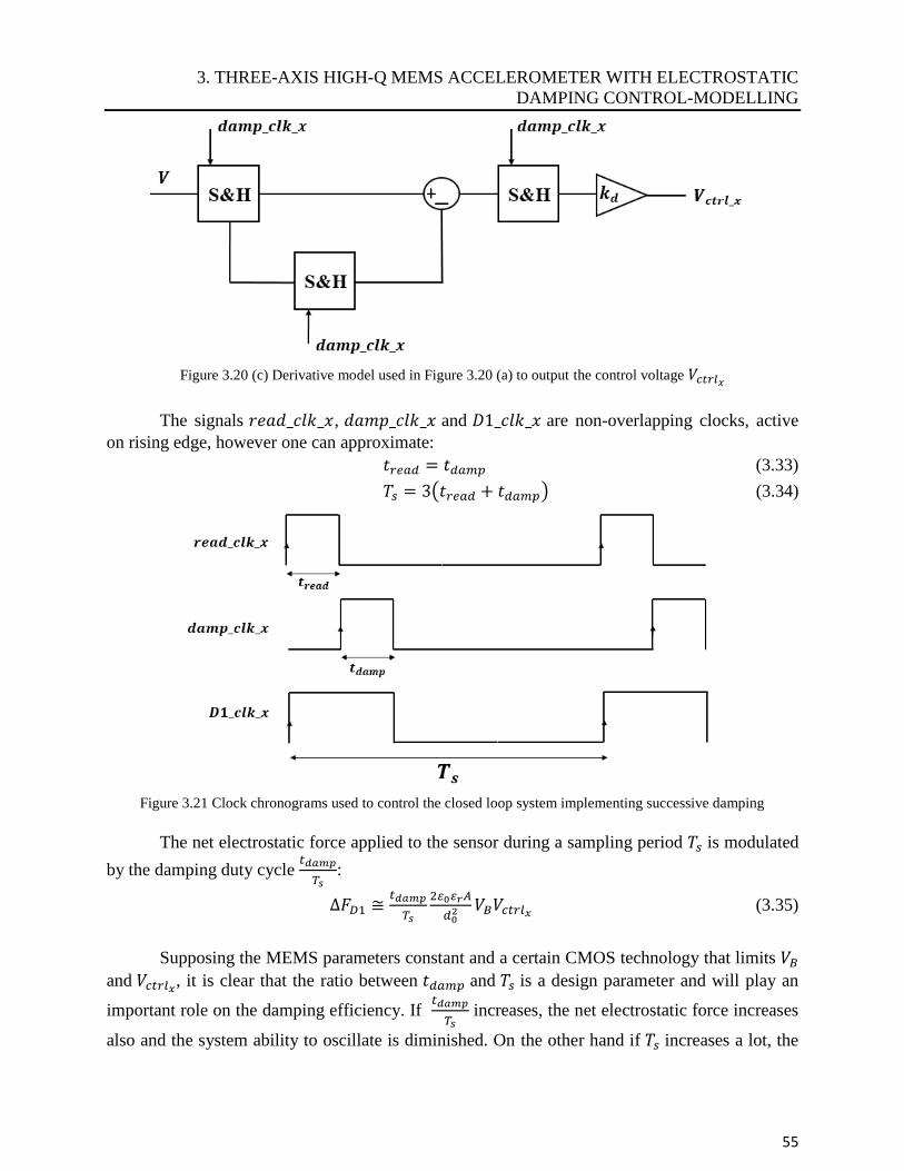
3. THREE-AXIS HIGH-Q MEMS ACCELEROMETER WITH ELECTROSTATIC
DAMPING CONTROL-MODELLING
55
Figure 3.20 (c) Derivative model used in Figure 3.20 (a) to output the control voltage 𝑉𝑐𝑡𝑟𝑙𝑥
The signals 𝑟𝑒𝑎𝑑_𝑐𝑙𝑘_𝑥, 𝑑𝑎𝑚𝑝_𝑐𝑙𝑘_𝑥 and 𝐷1_𝑐𝑙𝑘_𝑥 are non-overlapping clocks, active
on rising edge, however one can approximate:
𝑡𝑟𝑒𝑎𝑑 = 𝑡𝑑𝑎𝑚𝑝 (3.33)
𝑇𝑠 = 3(𝑡𝑟𝑒𝑎𝑑 + 𝑡𝑑𝑎𝑚𝑝) (3.34)
Figure 3.21 Clock chronograms used to control the closed loop system implementing successive damping
The net electrostatic force applied to the sensor during a sampling period 𝑇𝑠 is modulated
by the damping duty cycle 𝑡𝑑𝑎𝑚𝑝
𝑇𝑠:
∆𝐹𝐷1 ≅𝑡𝑑𝑎𝑚𝑝
𝑇𝑠
2𝜀0𝜀𝑟𝐴
𝑑02 𝑉𝐵𝑉𝑐𝑡𝑟𝑙𝑥
(3.35)
Supposing the MEMS parameters constant and a certain CMOS technology that limits 𝑉𝐵
and 𝑉𝑐𝑡𝑟𝑙𝑥, it is clear that the ratio between 𝑡𝑑𝑎𝑚𝑝 and 𝑇𝑠 is a design parameter and will play an
important role on the damping efficiency. If 𝑡𝑑𝑎𝑚𝑝
𝑇𝑠 increases, the net electrostatic force increases
also and the system ability to oscillate is diminished. On the other hand if 𝑇𝑠 increases a lot, the
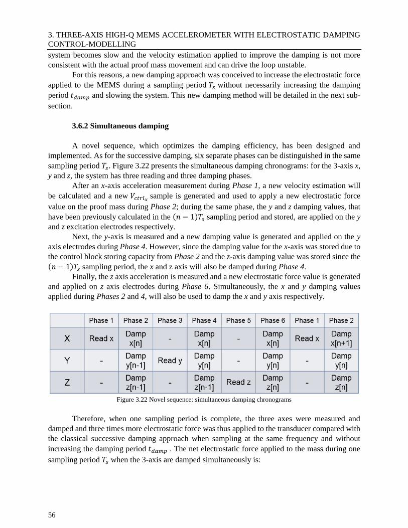
3. THREE-AXIS HIGH-Q MEMS ACCELEROMETER WITH ELECTROSTATIC DAMPING
CONTROL-MODELLING
56
system becomes slow and the velocity estimation applied to improve the damping is not more
consistent with the actual proof mass movement and can drive the loop unstable. For this reasons, a new damping approach was conceived to increase the electrostatic force
applied to the MEMS during a sampling period 𝑇𝑠 without necessarily increasing the damping
period 𝑡𝑑𝑎𝑚𝑝 and slowing the system. This new damping method will be detailed in the next sub-
section.
3.6.2 Simultaneous damping
A novel sequence, which optimizes the damping efficiency, has been designed and
implemented. As for the successive damping, six separate phases can be distinguished in the same
sampling period 𝑇𝑠. Figure 3.22 presents the simultaneous damping chronograms: for the 3-axis x,
y and z, the system has three reading and three damping phases.
After an x-axis acceleration measurement during Phase 1, a new velocity estimation will
be calculated and a new 𝑉𝑐𝑡𝑟𝑙𝑥 sample is generated and used to apply a new electrostatic force
value on the proof mass during Phase 2; during the same phase, the y and z damping values, that
have been previously calculated in the (𝑛 − 1)𝑇𝑠 sampling period and stored, are applied on the y
and z excitation electrodes respectively. Next, the y-axis is measured and a new damping value is generated and applied on the y
axis electrodes during Phase 4. However, since the damping value for the x-axis was stored due to
the control block storing capacity from Phase 2 and the z-axis damping value was stored since the
(𝑛 − 1)𝑇𝑠 sampling period, the x and z axis will also be damped during Phase 4. Finally, the z axis acceleration is measured and a new electrostatic force value is generated
and applied on z axis electrodes during Phase 6. Simultaneously, the x and y damping values
applied during Phases 2 and 4, will also be used to damp the x and y axis respectively.
Figure 3.22 Novel sequence: simultaneous damping chronograms
Therefore, when one sampling period is complete, the three axes were measured and
damped and three times more electrostatic force was thus applied to the transducer compared with
the classical successive damping approach when sampling at the same frequency and without
increasing the damping period 𝑡𝑑𝑎𝑚𝑝 . The net electrostatic force applied to the mass during one
sampling period 𝑇𝑠 when the 3-axis are damped simultaneously is:
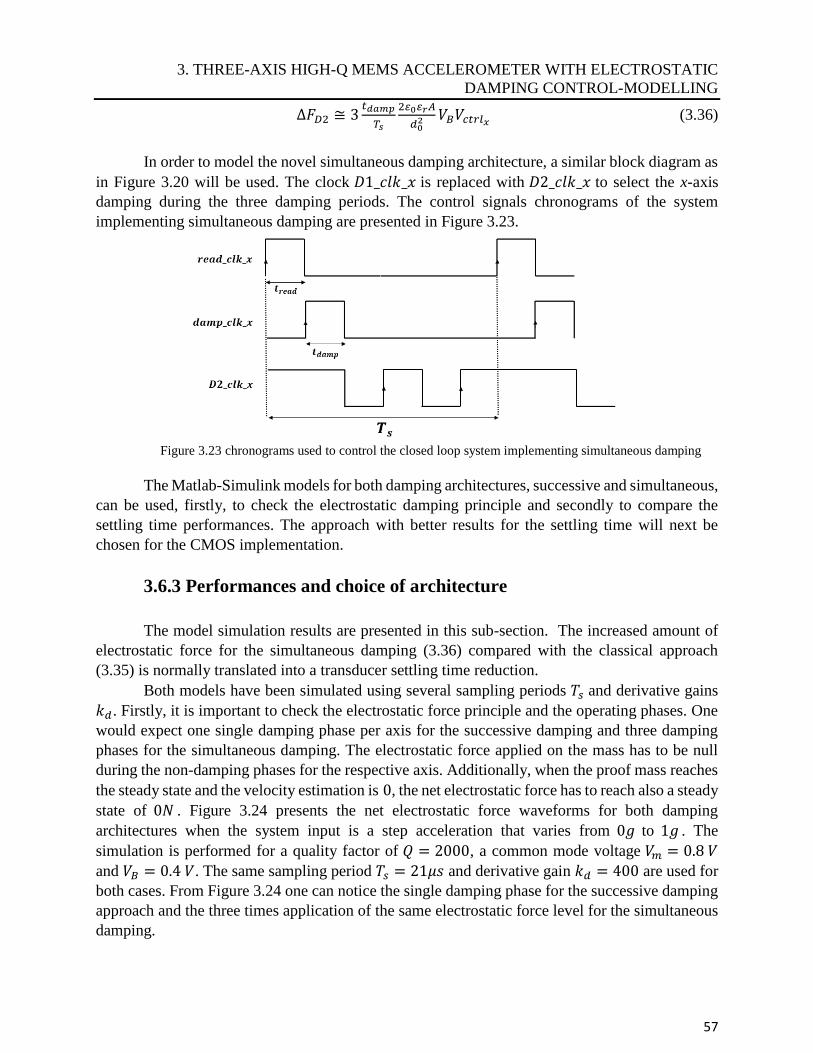
3. THREE-AXIS HIGH-Q MEMS ACCELEROMETER WITH ELECTROSTATIC
DAMPING CONTROL-MODELLING
57
∆𝐹𝐷2 ≅ 3𝑡𝑑𝑎𝑚𝑝
𝑇𝑠
2𝜀0𝜀𝑟𝐴
𝑑02 𝑉𝐵𝑉𝑐𝑡𝑟𝑙𝑥
(3.36)
In order to model the novel simultaneous damping architecture, a similar block diagram as
in Figure 3.20 will be used. The clock 𝐷1_𝑐𝑙𝑘_𝑥 is replaced with 𝐷2_𝑐𝑙𝑘_𝑥 to select the x-axis
damping during the three damping periods. The control signals chronograms of the system
implementing simultaneous damping are presented in Figure 3.23.
Figure 3.23 chronograms used to control the closed loop system implementing simultaneous damping
The Matlab-Simulink models for both damping architectures, successive and simultaneous,
can be used, firstly, to check the electrostatic damping principle and secondly to compare the
settling time performances. The approach with better results for the settling time will next be
chosen for the CMOS implementation.
3.6.3 Performances and choice of architecture
The model simulation results are presented in this sub-section. The increased amount of
electrostatic force for the simultaneous damping (3.36) compared with the classical approach
(3.35) is normally translated into a transducer settling time reduction.
Both models have been simulated using several sampling periods 𝑇𝑠 and derivative gains
𝑘𝑑. Firstly, it is important to check the electrostatic force principle and the operating phases. One
would expect one single damping phase per axis for the successive damping and three damping
phases for the simultaneous damping. The electrostatic force applied on the mass has to be null
during the non-damping phases for the respective axis. Additionally, when the proof mass reaches
the steady state and the velocity estimation is 0, the net electrostatic force has to reach also a steady
state of 0𝑁 . Figure 3.24 presents the net electrostatic force waveforms for both damping
architectures when the system input is a step acceleration that varies from 0𝑔 to 1𝑔 . The
simulation is performed for a quality factor of 𝑄 = 2000, a common mode voltage 𝑉𝑚 = 0.8 𝑉
and 𝑉𝐵 = 0.4 𝑉. The same sampling period 𝑇𝑠 = 21𝜇𝑠 and derivative gain 𝑘𝑑 = 400 are used for
both cases. From Figure 3.24 one can notice the single damping phase for the successive damping
approach and the three times application of the same electrostatic force level for the simultaneous
damping.
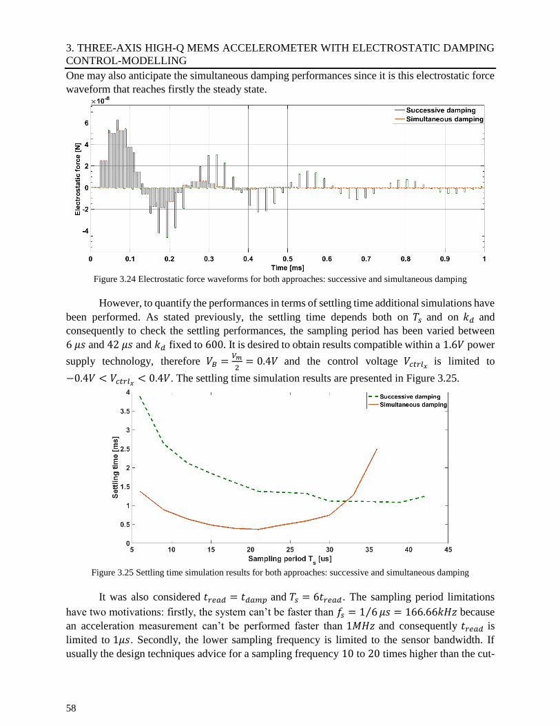
3. THREE-AXIS HIGH-Q MEMS ACCELEROMETER WITH ELECTROSTATIC DAMPING
CONTROL-MODELLING
58
One may also anticipate the simultaneous damping performances since it is this electrostatic force
waveform that reaches firstly the steady state.
Figure 3.24 Electrostatic force waveforms for both approaches: successive and simultaneous damping
However, to quantify the performances in terms of settling time additional simulations have
been performed. As stated previously, the settling time depends both on 𝑇𝑠 and on 𝑘𝑑 and
consequently to check the settling performances, the sampling period has been varied between
6 𝜇𝑠 and 42 𝜇𝑠 and 𝑘𝑑 fixed to 600. It is desired to obtain results compatible within a 1.6𝑉 power
supply technology, therefore 𝑉𝐵 =𝑉𝑚
2= 0.4𝑉 and the control voltage 𝑉𝑐𝑡𝑟𝑙𝑥
is limited to
−0.4𝑉 < 𝑉𝑐𝑡𝑟𝑙𝑥< 0.4𝑉. The settling time simulation results are presented in Figure 3.25.
Figure 3.25 Settling time simulation results for both approaches: successive and simultaneous damping
It was also considered 𝑡𝑟𝑒𝑎𝑑 = 𝑡𝑑𝑎𝑚𝑝 and 𝑇𝑠 = 6𝑡𝑟𝑒𝑎𝑑 . The sampling period limitations
have two motivations: firstly, the system can’t be faster than 𝑓𝑠 = 1 6⁄ 𝜇𝑠 = 166.66𝑘𝐻𝑧 because
an acceleration measurement can’t be performed faster than 1𝑀𝐻𝑧 and consequently 𝑡𝑟𝑒𝑎𝑑 is
limited to 1𝜇𝑠. Secondly, the lower sampling frequency is limited to the sensor bandwidth. If
usually the design techniques advice for a sampling frequency 10 to 20 times higher than the cut-
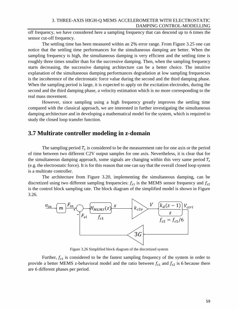
3. THREE-AXIS HIGH-Q MEMS ACCELEROMETER WITH ELECTROSTATIC
DAMPING CONTROL-MODELLING
59
off frequency, we have considered here a sampling frequency that can descend up to 6 times the
sensor cut-off frequency.
The settling time has been measured within an 2% error range. From Figure 3.25 one can
notice that the settling time performances for the simultaneous damping are better. When the
sampling frequency is high, the simultaneous damping is very efficient and the settling time is
roughly three times smaller than for the successive damping. Then, when the sampling frequency
starts decreasing, the successive damping architecture can be a better choice. The intuitive
explanation of the simultaneous damping performances degradation at low sampling frequencies
is the incoherence of the electrostatic force value during the second and the third damping phase.
When the sampling period is large, it is expected to apply on the excitation electrodes, during the
second and the third damping phase, a velocity estimation which is no more corresponding to the
real mass movement.
However, since sampling using a high frequency greatly improves the settling time
compared with the classical approach, we are interested in further investigating the simultaneous
damping architecture and in developing a mathematical model for the system, which is required to
study the closed loop transfer function.
3.7 Multirate controller modeling in z-domain
The sampling period 𝑇𝑠 is considered to be the measurement rate for one axis or the period
of time between two different C2V output samples for one axis. Nevertheless, it is clear that for
the simultaneous damping approach, some signals are changing within this very same period 𝑇𝑠
(e.g. the electrostatic force). It is for this reason that one can say that the overall closed loop system
is a multirate controller. The architecture from Figure 3.20, implementing the simultaneous damping, can be
discretized using two different sampling frequencies: 𝑓𝑠1 is the MEMS sensor frequency and 𝑓𝑠2
is the control block sampling rate. The block diagram of the simplified model is shown in Figure
3.26.
Figure 3.26 Simplified block diagram of the discretized system
Further, 𝑓𝑠1 is considered to be the fastest sampling frequency of the system in order to
provide a better MEMS z-behavioral model and the ratio between 𝑓𝑠1 and 𝑓𝑠2 is 6 because there
are 6 different phases per period.
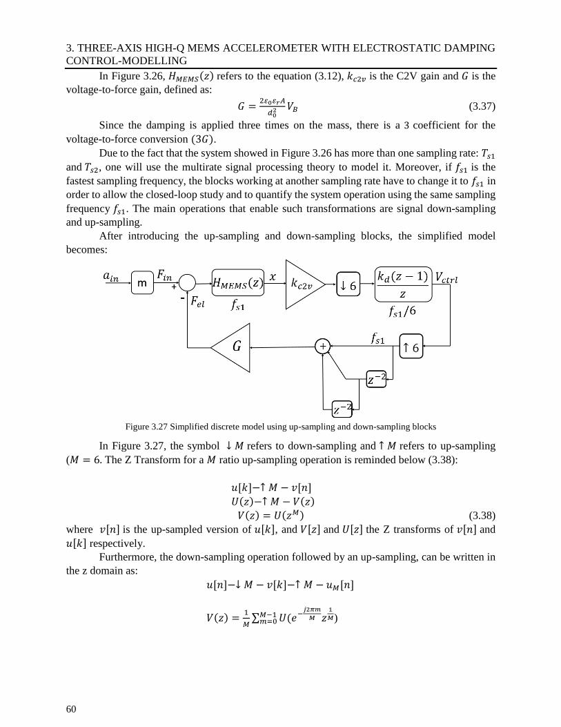
3. THREE-AXIS HIGH-Q MEMS ACCELEROMETER WITH ELECTROSTATIC DAMPING
CONTROL-MODELLING
60
In Figure 3.26, 𝐻𝑀𝐸𝑀𝑆(𝑧) refers to the equation (3.12), 𝑘𝑐2𝑣 is the C2V gain and 𝐺 is the
voltage-to-force gain, defined as:
𝐺 =2𝜀0𝜀𝑟𝐴
𝑑02 𝑉𝐵 (3.37)
Since the damping is applied three times on the mass, there is a 3 coefficient for the
voltage-to-force conversion (3𝐺).
Due to the fact that the system showed in Figure 3.26 has more than one sampling rate: 𝑇𝑠1
and 𝑇𝑠2, one will use the multirate signal processing theory to model it. Moreover, if 𝑓𝑠1 is the
fastest sampling frequency, the blocks working at another sampling rate have to change it to 𝑓𝑠1 in
order to allow the closed-loop study and to quantify the system operation using the same sampling
frequency 𝑓𝑠1. The main operations that enable such transformations are signal down-sampling
and up-sampling. After introducing the up-sampling and down-sampling blocks, the simplified model
becomes:
Figure 3.27 Simplified discrete model using up-sampling and down-sampling blocks
In Figure 3.27, the symbol ↓ 𝑀 refers to down-sampling and ↑ 𝑀 refers to up-sampling
(𝑀 = 6. The Z Transform for a 𝑀 ratio up-sampling operation is reminded below (3.38):
𝑢[𝑘]−↑ 𝑀 − 𝑣[𝑛]
𝑈(𝑧)−↑ 𝑀 − 𝑉(𝑧)
𝑉(𝑧) = 𝑈(𝑧𝑀) (3.38)
where 𝑣[𝑛] is the up-sampled version of 𝑢[𝑘], and 𝑉[𝑧] and 𝑈[𝑧] the Z transforms of 𝑣[𝑛] and
𝑢[𝑘] respectively.
Furthermore, the down-sampling operation followed by an up-sampling, can be written in
the z domain as:
𝑢[𝑛]−↓ 𝑀 − 𝑣[𝑘]−↑ 𝑀 − 𝑢𝑀[𝑛]
𝑉(𝑧) =1
𝑀∑ 𝑈(𝑒−
𝑗2𝜋𝑚
𝑀 𝑧1
𝑀𝑀−1𝑚=0 )
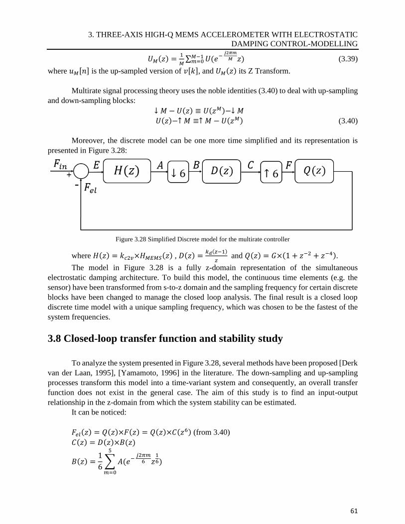
3. THREE-AXIS HIGH-Q MEMS ACCELEROMETER WITH ELECTROSTATIC
DAMPING CONTROL-MODELLING
61
𝑈𝑀(𝑧) =1
𝑀∑ 𝑈(𝑒−
𝑗2𝜋𝑚
𝑀 𝑧)𝑀−1𝑚=0 (3.39)
where 𝑢𝑀[𝑛] is the up-sampled version of 𝑣[𝑘], and 𝑈𝑀(𝑧) its Z Transform.
Multirate signal processing theory uses the noble identities (3.40) to deal with up-sampling
and down-sampling blocks:
↓ 𝑀 − 𝑈(𝑧) ≡ 𝑈(𝑧𝑀)−↓ 𝑀
𝑈(𝑧)−↑ 𝑀 ≡↑ 𝑀 − 𝑈(𝑧𝑀) (3.40)
Moreover, the discrete model can be one more time simplified and its representation is
presented in Figure 3.28:
Figure 3.28 Simplified Discrete model for the multirate controller
where 𝐻(𝑧) = 𝑘𝑐2𝑣×𝐻𝑀𝐸𝑀𝑆(𝑧) , 𝐷(𝑧) =𝑘𝑑(𝑧−1)
𝑧 and 𝑄(𝑧) = 𝐺×(1 + 𝑧−2 + 𝑧−4).
The model in Figure 3.28 is a fully z-domain representation of the simultaneous
electrostatic damping architecture. To build this model, the continuous time elements (e.g. the
sensor) have been transformed from s-to-z domain and the sampling frequency for certain discrete
blocks have been changed to manage the closed loop analysis. The final result is a closed loop
discrete time model with a unique sampling frequency, which was chosen to be the fastest of the
system frequencies.
3.8 Closed-loop transfer function and stability study
To analyze the system presented in Figure 3.28, several methods have been proposed [Derk
van der Laan, 1995], [Yamamoto, 1996] in the literature. The down-sampling and up-sampling
processes transform this model into a time-variant system and consequently, an overall transfer
function does not exist in the general case. The aim of this study is to find an input-output
relationship in the z-domain from which the system stability can be estimated.
It can be noticed:
𝐹𝑒𝑙(𝑧) = 𝑄(𝑧)×𝐹(𝑧) = 𝑄(𝑧)×𝐶(𝑧6) (from 3.40)
𝐶(𝑧) = 𝐷(𝑧)×𝐵(𝑧)
𝐵(𝑧) =1
6∑ 𝐴(𝑒−
𝑗2𝜋𝑚6 𝑧
16)
5
𝑚=0
3. THREE-AXIS HIGH-Q MEMS ACCELEROMETER WITH ELECTROSTATIC DAMPING
CONTROL-MODELLING
62
𝐵(𝑧6) =1
6∑ 𝐴 (𝑒−
𝑗2𝜋𝑚
6 𝑧)5𝑚=0 (from 3.34)
𝐴(𝑧) = 𝐻(𝑧)×𝐸(𝑧)
𝐸(𝑧) = 𝐹𝑖𝑛(𝑧) − 𝐹𝑒𝑙(𝑧)
𝐶(𝑧6) = 𝐷(𝑧6)×𝐵(𝑧6) = 𝐷(𝑧6)×1
6∑ 𝐴 (𝑒−
𝑗2𝜋𝑚6 𝑧) =
5
𝑚=0
𝐷(𝑧6)×1
6∑ 𝐻 (𝑒−
𝑗2𝜋𝑚6 𝑧)
5
𝑚=0
×𝐸 (𝑒− 𝑗2𝜋𝑚
6 𝑧) =
𝐷(𝑧6)×1
6∑ 𝐻 (𝑒−
𝑗2𝜋𝑚6 𝑧)
5
𝑚=0
× (𝐹𝑖𝑛 (𝑒− 𝑗2𝜋𝑚
6 𝑧) − 𝐹𝑒𝑙 (𝑒− 𝑗2𝜋𝑚
6 𝑧)) =
= 𝐷(𝑧6)× [(1
6∑ 𝐻 (𝑒−
𝑗2𝜋𝑚
6 𝑧)5𝑚=0 ×𝐹𝑖𝑛 (𝑒−
𝑗2𝜋𝑚
6 𝑧)) − (1
6∑ 𝐻 (𝑒−
𝑗2𝜋𝑚
6 𝑧)5𝑚=0 ×
𝐹𝑒𝑙 (𝑒−𝑗2𝜋𝑚
6 𝑧))] (3.41)
Then:
∑ 𝐹𝑒𝑙(𝑒− 𝑗2𝜋𝑚
6 𝑧)
5
𝑚=0
= ∑ 𝑄(𝑒− 𝑗2𝜋𝑚
6 𝑧)×𝐶(𝑒− 𝑗2𝜋𝑚
6×6𝑧6)
5
𝑚=0
(3.42)
But 𝐶(𝑒−𝑗2𝜋𝑚𝑧6) = 𝐶(𝑧6).
Replacing (3.42) in (3.41), equation (3.41) can be rewritten:
𝐶(𝑧6) = 𝐷(𝑧6)×1
6[(∑ 𝐻 (𝑒−
𝑗2𝜋𝑚
6 𝑧)5𝑚=0 ×𝐹𝑖𝑛 (𝑒−
𝑗2𝜋𝑚
6 𝑧)) − 𝐶(𝑧6)× (∑ 𝐻 (𝑒− 𝑗2𝜋𝑚
6 𝑧)5𝑚=0 ×
𝑄 (𝑒− 𝑗2𝜋𝑚
6 𝑧))]
𝐶(𝑧6) =𝐷(𝑧6)×
16
∑ 𝐻(𝑒− 𝑗2𝜋𝑚
6 𝑧)5𝑚=0 ×𝐹𝑖𝑛 (𝑒−
𝑗2𝜋𝑚6 𝑧)
1 + 𝐷(𝑧6)×16
∑ 𝐻 (𝑒− 𝑗2𝜋𝑚
6 𝑧)5𝑚=0 ×𝑄 (𝑒−
𝑗2𝜋𝑚6 𝑧)
𝐹𝑒𝑙(𝑧) = 𝑄(𝑧)×𝐶(𝑧6) =𝐷(𝑧6)×𝑄(𝑧)×
16
∑ 𝐻 (𝑒− 𝑗2𝜋𝑚
6 𝑧)5𝑚=0 ×𝐹𝑖𝑛 (𝑒−
𝑗2𝜋𝑚6 𝑧)
1 + 𝐷(𝑧6)×16
∑ 𝐻 (𝑒− 𝑗2𝜋𝑚
6 𝑧)5𝑚=0 ×𝑄 (𝑒−
𝑗2𝜋𝑚6 𝑧)
(3.43)
If we define 𝐾(𝑧) as:
𝐾(𝑧) =𝐷(𝑧6)×𝑄(𝑧)
1 + 𝐷(𝑧6)×16
∑ 𝐻 (𝑒− 𝑗2𝜋𝑚
6 𝑧)5𝑚=0 ×𝑄 (𝑒−
𝑗2𝜋𝑚6 𝑧)
(3.44)
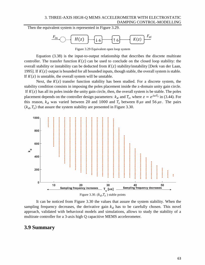
3. THREE-AXIS HIGH-Q MEMS ACCELEROMETER WITH ELECTROSTATIC
DAMPING CONTROL-MODELLING
63
Then the equivalent system is represented in Figure 3.29.
Figure 3.29 Equivalent open loop system
Equation (3.38) is the input-to-output relationship that describes the discrete multirate
controller. The transfer function 𝐾(𝑧) can be used to conclude on the closed loop stability: the
overall stability or instability can be deducted from 𝐾(𝑧) stability/instability [Derk van der Laan,
1995]. If 𝐾(𝑧) output is bounded for all bounded inputs, though stable, the overall system is stable.
If 𝐾(𝑧) is unstable, the overall system will be unstable.
Next, the 𝐾(𝑧) transfer function stability has been studied. For a discrete system, the
stability condition consists in imposing the poles placement inside the z-domain unity gain circle.
If 𝐾(𝑧) has all its poles inside the unity gain circle, then, the overall system is be stable. The poles
placement depends on the controller design parameters: 𝑘𝑑 and 𝑇𝑠, where 𝑧 = 𝑒𝑗𝜔𝑇𝑠 in (3.44). For
this reason, 𝑘𝑑 was varied between 20 and 1000 and 𝑇𝑠 between 8 𝜇𝑠 and 56 𝜇𝑠 . The pairs
(𝑘𝑑, 𝑇𝑠) that assure the system stability are presented in Figure 3.30.
Figure 3.30. (𝑘𝑑,𝑇𝑠 ) stable points
It can be noticed from Figure 3.30 the values that assure the system stability. When the
sampling frequency decreases, the derivative gain 𝑘𝑑 has to be carefully chosen. This novel
approach, validated with behavioral models and simulations, allows to study the stability of a
multirate controller for a 3-axis high Q capacitive MEMS accelerometer.
3.9 Summary
3. THREE-AXIS HIGH-Q MEMS ACCELEROMETER WITH ELECTROSTATIC DAMPING
CONTROL-MODELLING
64
This chapter has proposed a new electrostatic damping architecture for a 3-axis
underdamped accelerometer and presents a block by block modeling approach. Firstly, the system
specifications and constraints have been set: single proof-mass mechanical sensing element
common to the three-axis, single charge-to-voltage converter shared between the three-axis, no
extra-damping electrodes, and no charge-pump circuit.
In this conditions, a new damping configuration based on the velocity estimation principle,
allowing to improve the settling time has been developed, modeled and validated. The
simultaneous damping approach is using the storing properties of the controller: by simply storing
and applying the same amount of electrostatic force during the same sampling period, the settling
time can be improved with a ratio of three compared with the classical damping approach.
Finally, a new approach that uses multirate signal processing techniques as the up-sampling
and the down-sampling, has been introduced and validated. This method is required to determine
the design parameters assuring a stable closed-loop operation.
Considering the settling time performances presented in Figure 3.25 and the stability
simulation results showed in Figure 3.30, it was chosen for the system CMOS implementation a
sampling period of 𝑇𝑠 = 24 𝜇𝑠 and a derivative gain 𝑘𝑑 = 300. Increasing more the sampling
frequency and the derivative gain values leads to a settling time reduction but the design challenges
in terms of op-amp bandwidths and single stage gain architecture become notable.
Next chapter introduces the CMOS implementation of the architecture defined in this
chapter. The overall accelerometer signal chain (C2V, derivative and analog gain stages) has been
designed to fulfill the low power constraint of the system; the damping efficiency is assessed using
closed loop simulations results and comparisons with Matlab-Simulink models.
65
CHAPTER 4
TOWARDS A CMOS ANALOG FRONT-END FOR
A THREE-AXIS HIGH Q MEMS
ACCELEROMETER WITH SIMULTANEOUS
DAMPING CONTROL
Based on the previous analysis and successful modeling of the proposed closed loop
accelerometer architecture, the corresponding CMOS analog front-end can now be designed. This
chapter presents the block-by-block design of a low-power analog front-end for a three-axis
underdamped MEMS accelerometer with simultaneous damping control. Using a top-down
approach, a discrete-time switched-capacitor architecture is implemented in a 0.18𝜇𝑚 CMOS
TSMC process; the system architecture, already described and validated in Chapter 3, is translated
into a transistor design using Cadence Environment. A new VerilogA-Spectre model has been
developed for the three-axis MEMS accelerometer to enable the overall system simulation using
the Cadence software. Finally, closed-loop simulations are performed and the settling time method
is used to assess the damping efficiency.
4.1 System design of a low-power analog front-end for a three-axis
underdamped MEMS accelerometer with simultaneous electrostatic
damping control
The low-power specification of a consumer market sensor, as well as the electrodes
multiplexing requirement, make the switched-capacitor circuit approach much more appropriate
than the continuous time one. The sampling frequency is found using the stability analysis already
presented in Chapter 3. The choice of each sub-system topology is based either on low-power or
low-noise considerations. The connection between the integrated circuit and the MEMS is ensured through the proof-
mass itself. As a result, a fully-differential architecture can be designed for a fully differential
MEMS with a two-mass transducer. For the sake of simplicity, in this study, a single mass will be
connected to the C2V inverting input as presented in Figure 4.1; the common mode voltage of the
C2V is set to 𝑉𝑚 = 0.8𝑉. Next, the derivative block estimates the proof mass velocity, 𝑉𝑐𝑡𝑟𝑙𝑥, and
differentially outputs this quantity with respect to a common mode level which is 𝑉𝑚 + 𝑉𝐵 = 1.2𝑉.
Comparing the Derivative block outputs with equations (3.15), it can be noticed that the derivative
gain 𝑘𝑑 is missing from the excitation signals expressions during the damping phase. It is for this
reason that the next stage will add the derivative gain 𝑘𝑑. Finally, since during the reading phase
different excitation signals are applied on the transducer electrodes (𝑉𝑟𝑒𝑎𝑑 𝑥+ and 𝑉𝑟𝑒𝑎𝑑 𝑥−) an
excitation block is added in the loop. The excitation signals block consists in an analog multiplexer
controlled in such a way that either the reading or the damping excitation is applied on the sensor
electrodes at a predefined moment and during a certain amount of time. The y and z electrodes are
4. TOWARDS A CMOS ANALOG FRONT-END FOR A THREE-AXIS HIGH-Q MEMS
ACCELEROMETER WITH SIMULTANEOUS DAMPING CONTROL
95
connected to 𝑉𝑚 in order to create a null electrostatic force between these electrodes and the proof
mass and also to not perturb the x-axis measurement. With such a system, an acceleration applied
along the x-axis can be accurately measured even if the transducer has a high-quality factor. The
circuit is designed for a sampling frequency of 𝑇𝑠 = 24𝜇𝑠 and 𝑘𝑑 = 300 (Section 3.8) and is
working under an analog power supply of 𝑉𝑑𝑑𝑎 = 1.6𝑉 and a digital power supply of 𝑉𝑑𝑑𝑑 =1.75𝑉. Considering an ASIC implementation, the analog power supply is delivered by a bandgap
circuit. If the bandgap has a supply of 1.75𝑉, a 𝑉𝐷𝑆 of at least 0.15 𝑉 has to be assured on the
bandgap output p-channel transistor, resulting in an analog supply of 1.6𝑉. The digital supply
doesn’t have noise and perturbations sensitivity limitations and its value is decided by the
embedded digital library; here 1.75𝑉.
Figure 4.1. Block diagram of the accelerometer signal chain for x-axis
4.2 MEMS Accelerometer VerilogA – Spectre Model
In addition to the Matlab-Simulink models, a new MEMS accelerometer model is required
for the CMOS implementation in order to run complete system simulations. The transducer, for
which the design parameters have been presented in Table 3.1 and illustrated in Figure 3.2, was
modeled using the VerilogA language and integrated in the Cadence’Spectre simulator. The
modeling code is given in Appendices I and its associated symbol is shown in Figure 4.2. The model pins purpose is either to enable the Analog-Front-End connection or for tests
and validation. Firstly, the transducer can be stimulated along the three-directions x, y and z using
the input pins 𝑎𝑥, 𝑎𝑦 and 𝑎𝑧 to apply an external acceleration. Depending on the test nature, the
external acceleration can be a step, a sinusoidal acceleration or null, if for example, the self-test
capabilities are used.
4. TOWARDS A CMOS ANALOG FRONT-END FOR A THREE-AXIS HIGH-Q MEMS
ACCELEROMETER WITH SIMULTANEOUS DAMPING CONTROL
67
Further, the two moving masses can be accessed using the pins 𝑚1 or 𝑚2 , which are
connected to the C2V. Here, only 𝑚1 pin is connected to the C2V inverted input. The current
passing through the node 𝑚1 reflects the charge variation induced by the acceleration applied on
the mass. Then, each axis has two excitation plates, a positive and a negative one, that can be
inverted since the design is symmetrical: 𝑥1, 𝑥2, 𝑦1, 𝑦2 and 𝑧1, 𝑧2. If needed, parasitical effects of
the sensor shield or single-ended self-test modules can be modeled and implemented as well (𝑠𝑢𝑏
and 𝑠𝑡 are the associated pins for those capabilities). The two excitation plates and two proof masses result in four variable capacitances per
axis, twelve in total (𝑐𝑥11, 𝑐𝑥12, 𝑐𝑥21, 𝑐𝑥22, 𝑐𝑦11, 𝑐𝑦12, 𝑐𝑦21, 𝑐𝑦22, 𝑐𝑧11, 𝑐𝑧12, 𝑐𝑧21, 𝑐𝑧22 ) that change
their value under the effect of an external acceleration. The modeling convention is 1𝑉 for a 1𝑓𝐹
of capacitance. The transducer sensitivity is 1.125 𝑓𝐹 𝑔⁄ per side or 4.5 𝑓𝐹 𝑔⁄ per axis.
Figure 4.2. An illustration of the MEMS accelerometer Cadence symbol
𝐶𝑠𝑡1𝑏 and 𝐶𝑠𝑡2𝑎 refer to a one sided capacitor module for single ended self-test modules;
𝑑𝑖𝑠𝑝𝑥1, 𝑑𝑖𝑠𝑝𝑥2, 𝑑𝑖𝑠𝑝𝑦1, 𝑑𝑖𝑠𝑝𝑦2 can output the displacement of the proof masses 𝑚1, 𝑚2 when an
acceleration occurs (1𝑉 for a 1𝜇𝑚 of displacement). Regarding the z-axis, the sensor has a teeter-
tooter design and a rotational movement therefore the angle between the excitation plates and the
proof mass measure the extern acceleration. 𝑡ℎ𝑒𝑡𝑎𝑧1, 𝑡ℎ𝑒𝑡𝑎𝑧2 are the output monitor pins for z-
axis rotation (1𝑉 for a 1 radian of displacement).
The model is built as follows: the VerilogA language is used to describe the transducer
functioning. Then, the VerilogA model is included and appealed in a Spectre file. Parameters as
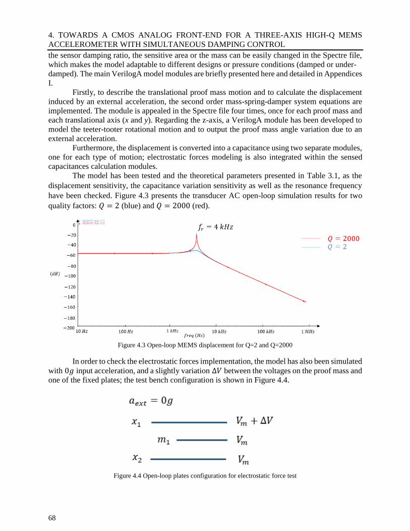
4. TOWARDS A CMOS ANALOG FRONT-END FOR A THREE-AXIS HIGH-Q MEMS
ACCELEROMETER WITH SIMULTANEOUS DAMPING CONTROL
68
the sensor damping ratio, the sensitive area or the mass can be easily changed in the Spectre file,
which makes the model adaptable to different designs or pressure conditions (damped or under-
damped). The main VerilogA model modules are briefly presented here and detailed in Appendices
I.
Firstly, to describe the translational proof mass motion and to calculate the displacement
induced by an external acceleration, the second order mass-spring-damper system equations are
implemented. The module is appealed in the Spectre file four times, once for each proof mass and
each translational axis (x and y). Regarding the z-axis, a VerilogA module has been developed to
model the teeter-tooter rotational motion and to output the proof mass angle variation due to an
external acceleration.
Furthermore, the displacement is converted into a capacitance using two separate modules,
one for each type of motion; electrostatic forces modeling is also integrated within the sensed
capacitances calculation modules.
The model has been tested and the theoretical parameters presented in Table 3.1, as the
displacement sensitivity, the capacitance variation sensitivity as well as the resonance frequency
have been checked. Figure 4.3 presents the transducer AC open-loop simulation results for two
quality factors: 𝑄 = 2 (blue) and 𝑄 = 2000 (red).
Figure 4.3 Open-loop MEMS displacement for Q=2 and Q=2000
In order to check the electrostatic forces implementation, the model has also been simulated
with 0𝑔 input acceleration, and a slightly variation ∆𝑉 between the voltages on the proof mass and
one of the fixed plates; the test bench configuration is shown in Figure 4.4.
Figure 4.4 Open-loop plates configuration for electrostatic force test
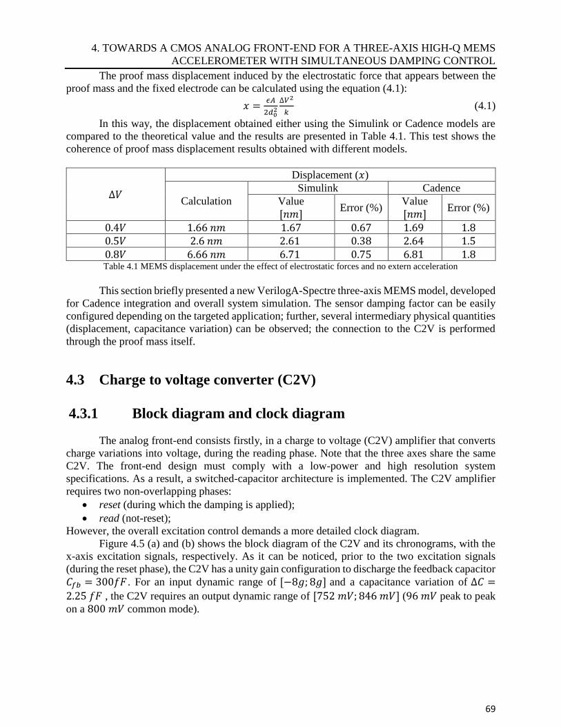
4. TOWARDS A CMOS ANALOG FRONT-END FOR A THREE-AXIS HIGH-Q MEMS
ACCELEROMETER WITH SIMULTANEOUS DAMPING CONTROL
69
The proof mass displacement induced by the electrostatic force that appears between the
proof mass and the fixed electrode can be calculated using the equation (4.1):
𝑥 =𝜖𝐴
2𝑑02
∆𝑉2
𝑘 (4.1)
In this way, the displacement obtained either using the Simulink or Cadence models are
compared to the theoretical value and the results are presented in Table 4.1. This test shows the
coherence of proof mass displacement results obtained with different models.
∆𝑉
Displacement (𝑥)
Calculation
Simulink Cadence Value
[𝑛𝑚] Error (%)
Value
[𝑛𝑚] Error (%)
0.4𝑉 1.66 𝑛𝑚 1.67 0.67 1.69 1.8
0.5𝑉 2.6 𝑛𝑚 2.61 0.38 2.64 1.5
0.8𝑉 6.66 𝑛𝑚 6.71 0.75 6.81 1.8 Table 4.1 MEMS displacement under the effect of electrostatic forces and no extern acceleration
This section briefly presented a new VerilogA-Spectre three-axis MEMS model, developed
for Cadence integration and overall system simulation. The sensor damping factor can be easily
configured depending on the targeted application; further, several intermediary physical quantities
(displacement, capacitance variation) can be observed; the connection to the C2V is performed
through the proof mass itself.
4.3 Charge to voltage converter (C2V)
4.3.1 Block diagram and clock diagram
The analog front-end consists firstly, in a charge to voltage (C2V) amplifier that converts
charge variations into voltage, during the reading phase. Note that the three axes share the same
C2V. The front-end design must comply with a low-power and high resolution system
specifications. As a result, a switched-capacitor architecture is implemented. The C2V amplifier
requires two non-overlapping phases:
• reset (during which the damping is applied); • read (not-reset);
However, the overall excitation control demands a more detailed clock diagram. Figure 4.5 (a) and (b) shows the block diagram of the C2V and its chronograms, with the
x-axis excitation signals, respectively. As it can be noticed, prior to the two excitation signals
(during the reset phase), the C2V has a unity gain configuration to discharge the feedback capacitor
𝐶𝑓𝑏 = 300𝑓𝐹 . For an input dynamic range of [−8𝑔; 8𝑔] and a capacitance variation of ∆𝐶 =
2.25 𝑓𝐹 , the C2V requires an output dynamic range of [752 𝑚𝑉; 846 𝑚𝑉] (96 𝑚𝑉 peak to peak
on a 800 𝑚𝑉 common mode).
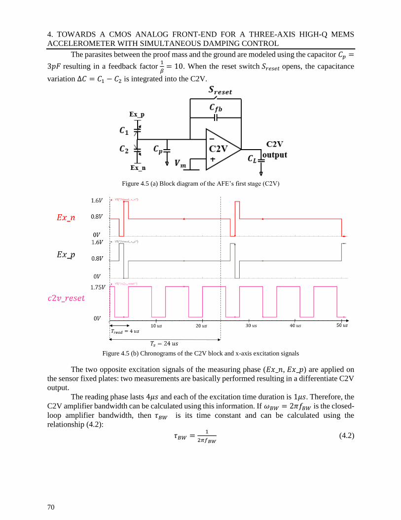
4. TOWARDS A CMOS ANALOG FRONT-END FOR A THREE-AXIS HIGH-Q MEMS
ACCELEROMETER WITH SIMULTANEOUS DAMPING CONTROL
70
The parasites between the proof mass and the ground are modeled using the capacitor 𝐶𝑝 =
3𝑝𝐹 resulting in a feedback factor 1
𝛽= 10. When the reset switch 𝑆𝑟𝑒𝑠𝑒𝑡 opens, the capacitance
variation ∆𝐶 = 𝐶1 − 𝐶2 is integrated into the C2V.
Figure 4.5 (a) Block diagram of the AFE’s first stage (C2V)
Figure 4.5 (b) Chronograms of the C2V block and x-axis excitation signals
The two opposite excitation signals of the measuring phase (𝐸𝑥_𝑛, 𝐸𝑥_𝑝) are applied on
the sensor fixed plates: two measurements are basically performed resulting in a differentiate C2V
output.
The reading phase lasts 4𝜇𝑠 and each of the excitation time duration is 1𝜇𝑠. Therefore, the
C2V amplifier bandwidth can be calculated using this information. If 𝜔𝐵𝑊 = 2𝜋𝑓𝐵𝑊 is the closed-
loop amplifier bandwidth, then 𝜏𝐵𝑊 is its time constant and can be calculated using the
relationship (4.2):
𝜏𝐵𝑊 =1
2𝜋𝑓𝐵𝑊 (4.2)
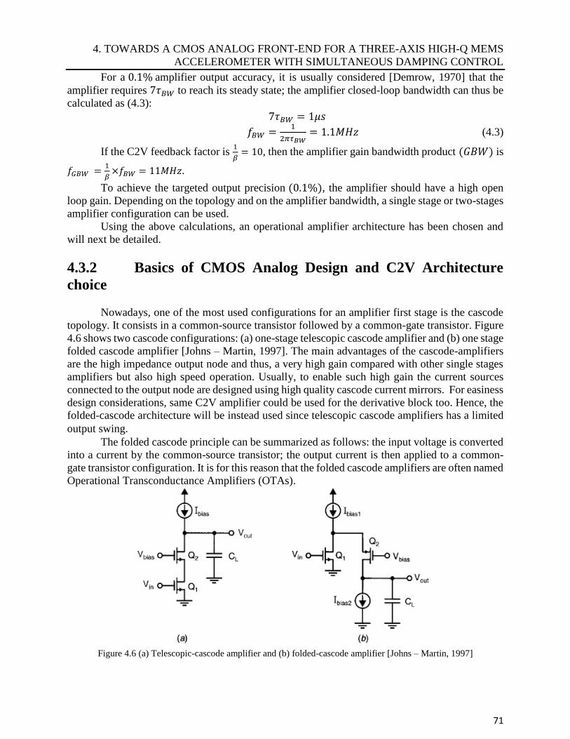
4. TOWARDS A CMOS ANALOG FRONT-END FOR A THREE-AXIS HIGH-Q MEMS
ACCELEROMETER WITH SIMULTANEOUS DAMPING CONTROL
71
For a 0.1% amplifier output accuracy, it is usually considered [Demrow, 1970] that the
amplifier requires 7𝜏𝐵𝑊 to reach its steady state; the amplifier closed-loop bandwidth can thus be
calculated as (4.3):
7𝜏𝐵𝑊 = 1𝜇𝑠
𝑓𝐵𝑊 =1
2𝜋𝜏𝐵𝑊= 1.1𝑀𝐻𝑧 (4.3)
If the C2V feedback factor is 1
𝛽= 10, then the amplifier gain bandwidth product (𝐺𝐵𝑊) is
𝑓𝐺𝐵𝑊 =
1
𝛽×𝑓𝐵𝑊 = 11𝑀𝐻𝑧.
To achieve the targeted output precision (0.1%), the amplifier should have a high open
loop gain. Depending on the topology and on the amplifier bandwidth, a single stage or two-stages
amplifier configuration can be used.
Using the above calculations, an operational amplifier architecture has been chosen and
will next be detailed.
4.3.2 Basics of CMOS Analog Design and C2V Architecture
choice
Nowadays, one of the most used configurations for an amplifier first stage is the cascode
topology. It consists in a common-source transistor followed by a common-gate transistor. Figure
4.6 shows two cascode configurations: (a) one-stage telescopic cascode amplifier and (b) one stage
folded cascode amplifier [Johns – Martin, 1997]. The main advantages of the cascode-amplifiers
are the high impedance output node and thus, a very high gain compared with other single stages
amplifiers but also high speed operation. Usually, to enable such high gain the current sources
connected to the output node are designed using high quality cascode current mirrors. For easiness
design considerations, same C2V amplifier could be used for the derivative block too. Hence, the
folded-cascode architecture will be instead used since telescopic cascode amplifiers has a limited
output swing. The folded cascode principle can be summarized as follows: the input voltage is converted
into a current by the common-source transistor; the output current is then applied to a common-
gate transistor configuration. It is for this reason that the folded cascode amplifiers are often named
Operational Transconductance Amplifiers (OTAs).
Figure 4.6 (a) Telescopic-cascode amplifier and (b) folded-cascode amplifier [Johns – Martin, 1997]
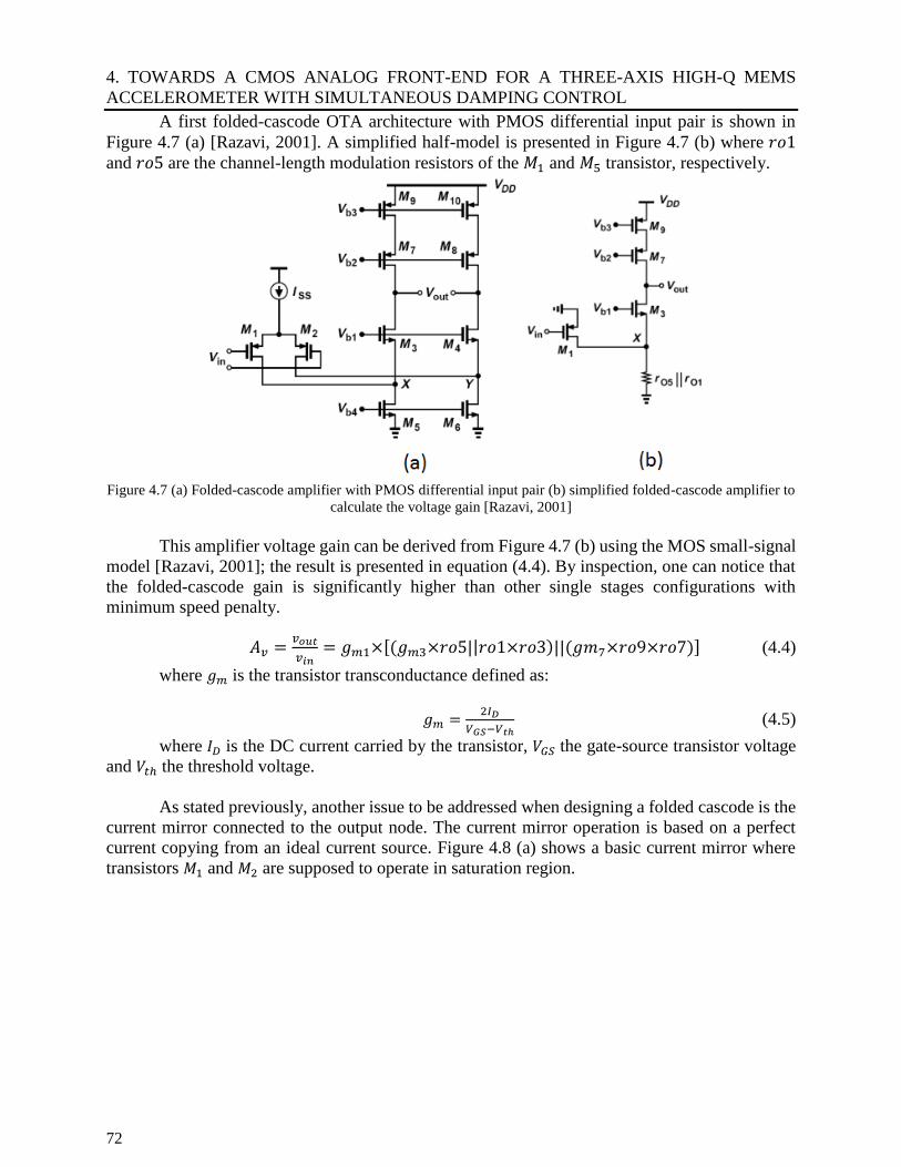
4. TOWARDS A CMOS ANALOG FRONT-END FOR A THREE-AXIS HIGH-Q MEMS
ACCELEROMETER WITH SIMULTANEOUS DAMPING CONTROL
72
A first folded-cascode OTA architecture with PMOS differential input pair is shown in
Figure 4.7 (a) [Razavi, 2001]. A simplified half-model is presented in Figure 4.7 (b) where 𝑟𝑜1
and 𝑟𝑜5 are the channel-length modulation resistors of the 𝑀1 and 𝑀5 transistor, respectively.
Figure 4.7 (a) Folded-cascode amplifier with PMOS differential input pair (b) simplified folded-cascode amplifier to
calculate the voltage gain [Razavi, 2001]
This amplifier voltage gain can be derived from Figure 4.7 (b) using the MOS small-signal
model [Razavi, 2001]; the result is presented in equation (4.4). By inspection, one can notice that
the folded-cascode gain is significantly higher than other single stages configurations with
minimum speed penalty.
𝐴𝑣 =𝑣𝑜𝑢𝑡
𝑣𝑖𝑛= 𝑔𝑚1×[(𝑔𝑚3×𝑟𝑜5||𝑟𝑜1×𝑟𝑜3)||(𝑔𝑚7×𝑟𝑜9×𝑟𝑜7)] (4.4)
where 𝑔𝑚 is the transistor transconductance defined as:
𝑔𝑚 =2𝐼𝐷
𝑉𝐺𝑆−𝑉𝑡ℎ (4.5)
where 𝐼𝐷 is the DC current carried by the transistor, 𝑉𝐺𝑆 the gate-source transistor voltage
and 𝑉𝑡ℎ the threshold voltage.
As stated previously, another issue to be addressed when designing a folded cascode is the
current mirror connected to the output node. The current mirror operation is based on a perfect
current copying from an ideal current source. Figure 4.8 (a) shows a basic current mirror where
transistors 𝑀1 and 𝑀2 are supposed to operate in saturation region.
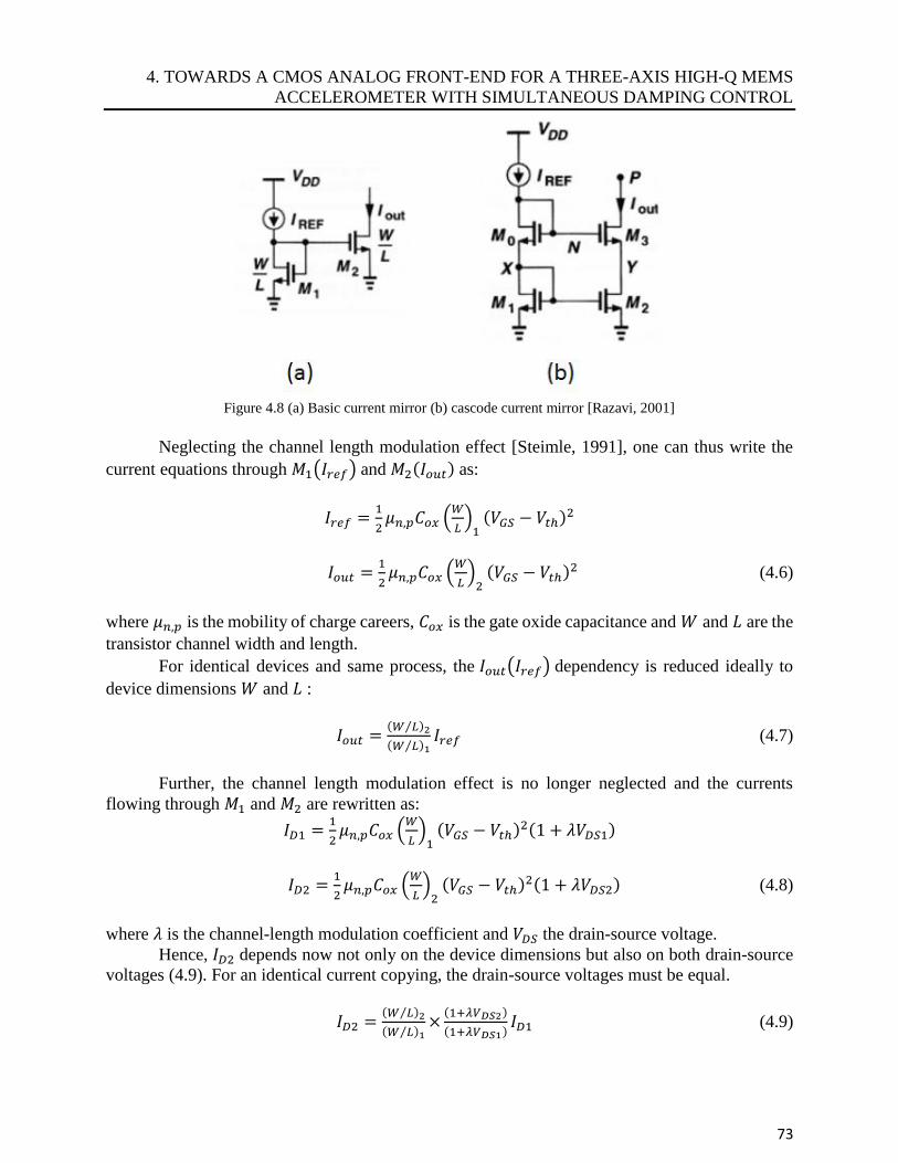
4. TOWARDS A CMOS ANALOG FRONT-END FOR A THREE-AXIS HIGH-Q MEMS
ACCELEROMETER WITH SIMULTANEOUS DAMPING CONTROL
73
Figure 4.8 (a) Basic current mirror (b) cascode current mirror [Razavi, 2001]
Neglecting the channel length modulation effect [Steimle, 1991], one can thus write the
current equations through 𝑀1(𝐼𝑟𝑒𝑓) and 𝑀2(𝐼𝑜𝑢𝑡) as:
𝐼𝑟𝑒𝑓 =1
2𝜇𝑛,𝑝𝐶𝑜𝑥 (
𝑊
𝐿)
1(𝑉𝐺𝑆 − 𝑉𝑡ℎ)2
𝐼𝑜𝑢𝑡 =1
2𝜇𝑛,𝑝𝐶𝑜𝑥 (
𝑊
𝐿)
2(𝑉𝐺𝑆 − 𝑉𝑡ℎ)2 (4.6)
where 𝜇𝑛,𝑝 is the mobility of charge careers, 𝐶𝑜𝑥 is the gate oxide capacitance and 𝑊 and 𝐿 are the
transistor channel width and length.
For identical devices and same process, the 𝐼𝑜𝑢𝑡(𝐼𝑟𝑒𝑓) dependency is reduced ideally to
device dimensions 𝑊 and 𝐿 :
𝐼𝑜𝑢𝑡 =(𝑊 𝐿⁄ )2
(𝑊 𝐿⁄ )1𝐼𝑟𝑒𝑓 (4.7)
Further, the channel length modulation effect is no longer neglected and the currents
flowing through 𝑀1 and 𝑀2 are rewritten as:
𝐼𝐷1 =1
2𝜇𝑛,𝑝𝐶𝑜𝑥 (
𝑊
𝐿)
1(𝑉𝐺𝑆 − 𝑉𝑡ℎ)2(1 + 𝜆𝑉𝐷𝑆1)
𝐼𝐷2 =1
2𝜇𝑛,𝑝𝐶𝑜𝑥 (
𝑊
𝐿)
2(𝑉𝐺𝑆 − 𝑉𝑡ℎ)2(1 + 𝜆𝑉𝐷𝑆2) (4.8)
where 𝜆 is the channel-length modulation coefficient and 𝑉𝐷𝑆 the drain-source voltage.
Hence, 𝐼𝐷2 depends now not only on the device dimensions but also on both drain-source
voltages (4.9). For an identical current copying, the drain-source voltages must be equal.
𝐼𝐷2 =(𝑊 𝐿⁄ )2
(𝑊 𝐿⁄ )1×
(1+𝜆𝑉𝐷𝑆2)
(1+𝜆𝑉𝐷𝑆1)𝐼𝐷1 (4.9)
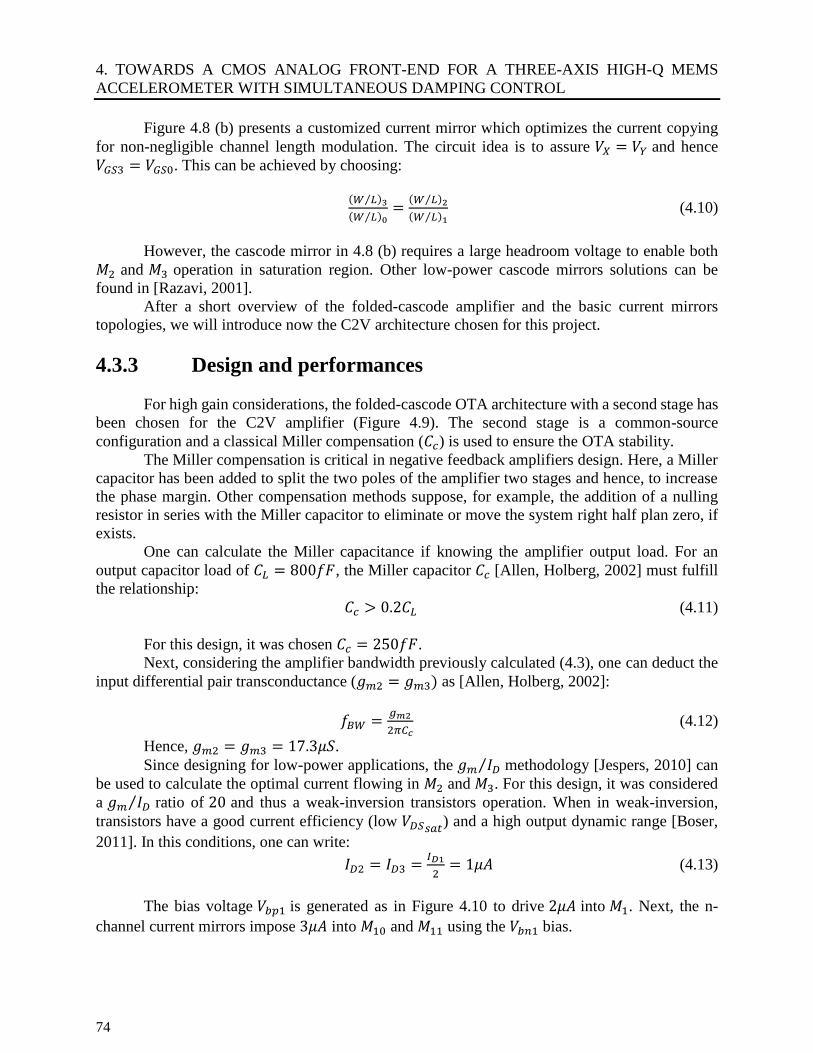
4. TOWARDS A CMOS ANALOG FRONT-END FOR A THREE-AXIS HIGH-Q MEMS
ACCELEROMETER WITH SIMULTANEOUS DAMPING CONTROL
74
Figure 4.8 (b) presents a customized current mirror which optimizes the current copying
for non-negligible channel length modulation. The circuit idea is to assure 𝑉𝑋 = 𝑉𝑌 and hence
𝑉𝐺𝑆3 = 𝑉𝐺𝑆0. This can be achieved by choosing:
(𝑊 𝐿⁄ )3
(𝑊 𝐿⁄ )0=
(𝑊 𝐿⁄ )2
(𝑊 𝐿⁄ )1 (4.10)
However, the cascode mirror in 4.8 (b) requires a large headroom voltage to enable both
𝑀2 and 𝑀3 operation in saturation region. Other low-power cascode mirrors solutions can be
found in [Razavi, 2001].
After a short overview of the folded-cascode amplifier and the basic current mirrors
topologies, we will introduce now the C2V architecture chosen for this project.
4.3.3 Design and performances
For high gain considerations, the folded-cascode OTA architecture with a second stage has
been chosen for the C2V amplifier (Figure 4.9). The second stage is a common-source
configuration and a classical Miller compensation (𝐶𝑐) is used to ensure the OTA stability. The Miller compensation is critical in negative feedback amplifiers design. Here, a Miller
capacitor has been added to split the two poles of the amplifier two stages and hence, to increase
the phase margin. Other compensation methods suppose, for example, the addition of a nulling
resistor in series with the Miller capacitor to eliminate or move the system right half plan zero, if
exists. One can calculate the Miller capacitance if knowing the amplifier output load. For an
output capacitor load of 𝐶𝐿 = 800𝑓𝐹, the Miller capacitor 𝐶𝑐 [Allen, Holberg, 2002] must fulfill
the relationship:
𝐶𝑐 > 0.2𝐶𝐿 (4.11)
For this design, it was chosen 𝐶𝑐 = 250𝑓𝐹.
Next, considering the amplifier bandwidth previously calculated (4.3), one can deduct the
input differential pair transconductance (𝑔𝑚2 = 𝑔𝑚3) as [Allen, Holberg, 2002]:
𝑓𝐵𝑊 =𝑔𝑚2
2𝜋𝐶𝑐 (4.12)
Hence, 𝑔𝑚2 = 𝑔𝑚3 = 17.3𝜇𝑆.
Since designing for low-power applications, the 𝑔𝑚 𝐼𝐷⁄ methodology [Jespers, 2010] can
be used to calculate the optimal current flowing in 𝑀2 and 𝑀3. For this design, it was considered
a 𝑔𝑚 𝐼𝐷⁄ ratio of 20 and thus a weak-inversion transistors operation. When in weak-inversion,
transistors have a good current efficiency (low 𝑉𝐷𝑆𝑠𝑎𝑡) and a high output dynamic range [Boser,
2011]. In this conditions, one can write:
𝐼𝐷2 = 𝐼𝐷3 =𝐼𝐷1
2= 1𝜇𝐴 (4.13)
The bias voltage 𝑉𝑏𝑝1 is generated as in Figure 4.10 to drive 2𝜇𝐴 into 𝑀1. Next, the n-
channel current mirrors impose 3𝜇𝐴 into 𝑀10 and 𝑀11 using the 𝑉𝑏𝑛1 bias.
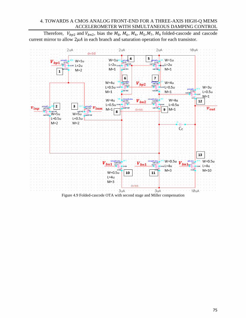
4. TOWARDS A CMOS ANALOG FRONT-END FOR A THREE-AXIS HIGH-Q MEMS
ACCELEROMETER WITH SIMULTANEOUS DAMPING CONTROL
75
Therefore, 𝑉𝑏𝑝2 and 𝑉𝑏𝑛2, bias the 𝑀8, 𝑀6, 𝑀4, 𝑀5,𝑀7, 𝑀9 folded-cascode and cascode
current mirror to allow 2𝜇𝐴 in each branch and saturation operation for each transistor.
Figure 4.9 Folded-cascode OTA with second stage and Miller compensation
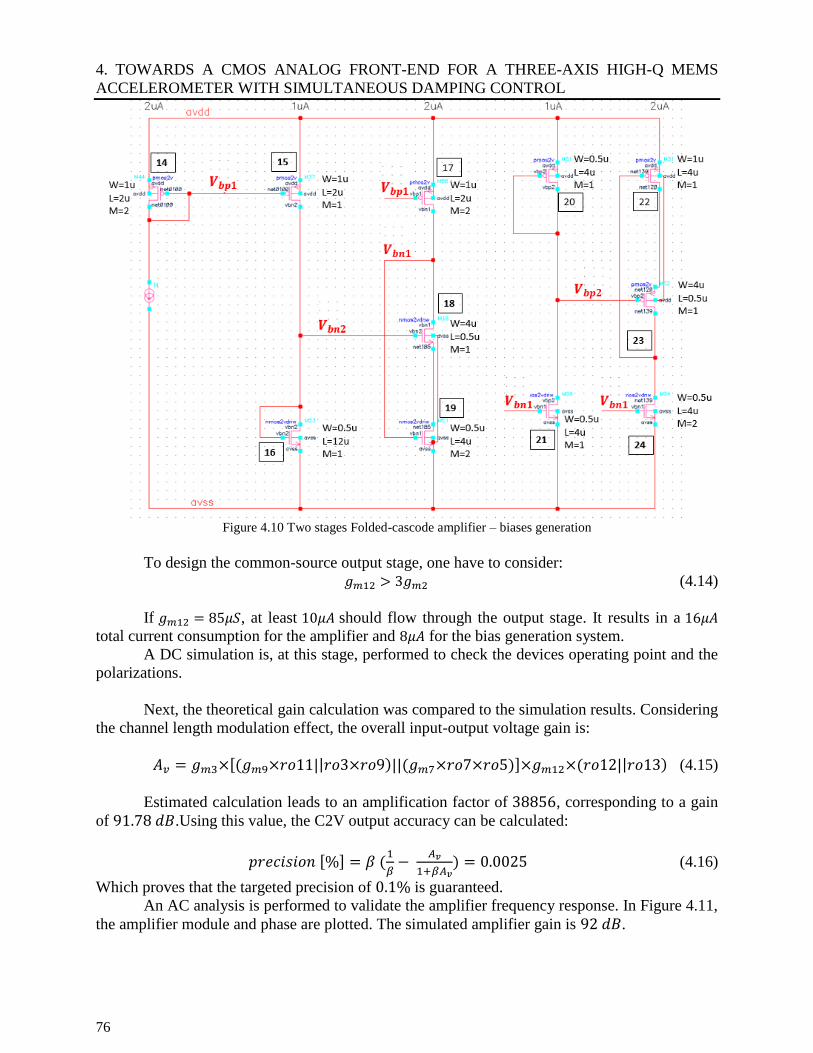
4. TOWARDS A CMOS ANALOG FRONT-END FOR A THREE-AXIS HIGH-Q MEMS
ACCELEROMETER WITH SIMULTANEOUS DAMPING CONTROL
76
Figure 4.10 Two stages Folded-cascode amplifier – biases generation
To design the common-source output stage, one have to consider:
𝑔𝑚12 > 3𝑔𝑚2 (4.14)
If 𝑔𝑚12 = 85𝜇𝑆, at least 10𝜇𝐴 should flow through the output stage. It results in a 16𝜇𝐴
total current consumption for the amplifier and 8𝜇𝐴 for the bias generation system.
A DC simulation is, at this stage, performed to check the devices operating point and the
polarizations.
Next, the theoretical gain calculation was compared to the simulation results. Considering
the channel length modulation effect, the overall input-output voltage gain is:
𝐴𝑣 = 𝑔𝑚3×[(𝑔𝑚9×𝑟𝑜11||𝑟𝑜3×𝑟𝑜9)||(𝑔𝑚7×𝑟𝑜7×𝑟𝑜5)]×𝑔𝑚12×(𝑟𝑜12||𝑟𝑜13) (4.15)
Estimated calculation leads to an amplification factor of 38856, corresponding to a gain
of 91.78 𝑑𝐵.Using this value, the C2V output accuracy can be calculated:
𝑝𝑟𝑒𝑐𝑖𝑠𝑖𝑜𝑛 [%] = 𝛽 (1
𝛽−
𝐴𝑣
1+𝛽𝐴𝑣) = 0.0025 (4.16)
Which proves that the targeted precision of 0.1% is guaranteed.
An AC analysis is performed to validate the amplifier frequency response. In Figure 4.11,
the amplifier module and phase are plotted. The simulated amplifier gain is 92 𝑑𝐵.
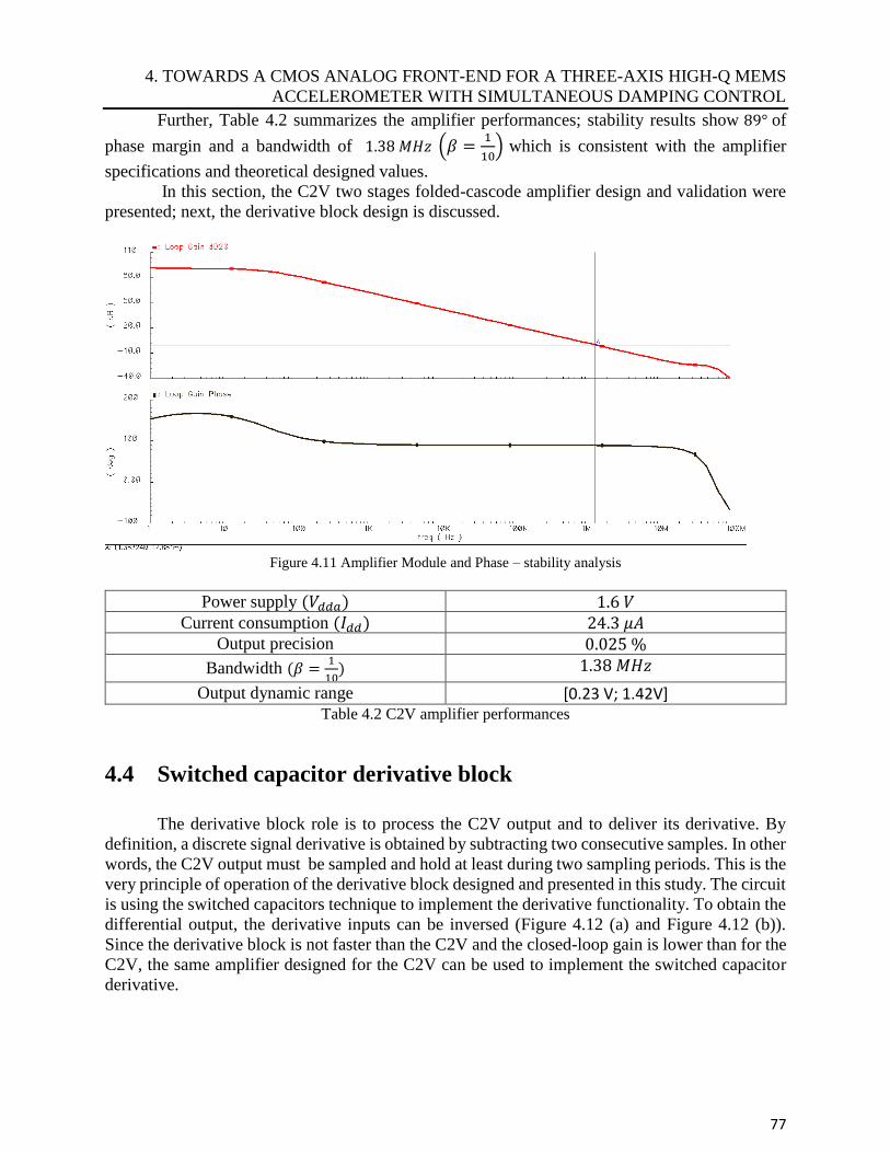
4. TOWARDS A CMOS ANALOG FRONT-END FOR A THREE-AXIS HIGH-Q MEMS
ACCELEROMETER WITH SIMULTANEOUS DAMPING CONTROL
77
Further, Table 4.2 summarizes the amplifier performances; stability results show 89° of
phase margin and a bandwidth of 1.38 𝑀𝐻𝑧 (𝛽 =1
10) which is consistent with the amplifier
specifications and theoretical designed values.
In this section, the C2V two stages folded-cascode amplifier design and validation were
presented; next, the derivative block design is discussed.
Figure 4.11 Amplifier Module and Phase – stability analysis
Power supply (𝑉𝑑𝑑𝑎) 1.6 𝑉 Current consumption (𝐼𝑑𝑑) 24.3 𝜇𝐴
Output precision 0.025 %
Bandwidth (𝛽 =1
10) 1.38 𝑀𝐻𝑧
Output dynamic range [0.23 V; 1.42V] Table 4.2 C2V amplifier performances
4.4 Switched capacitor derivative block
The derivative block role is to process the C2V output and to deliver its derivative. By
definition, a discrete signal derivative is obtained by subtracting two consecutive samples. In other
words, the C2V output must be sampled and hold at least during two sampling periods. This is the
very principle of operation of the derivative block designed and presented in this study. The circuit
is using the switched capacitors technique to implement the derivative functionality. To obtain the
differential output, the derivative inputs can be inversed (Figure 4.12 (a) and Figure 4.12 (b)).
Since the derivative block is not faster than the C2V and the closed-loop gain is lower than for the
C2V, the same amplifier designed for the C2V can be used to implement the switched capacitor
derivative.
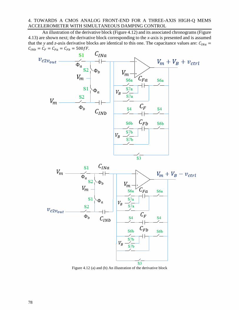
4. TOWARDS A CMOS ANALOG FRONT-END FOR A THREE-AXIS HIGH-Q MEMS
ACCELEROMETER WITH SIMULTANEOUS DAMPING CONTROL
78
An illustration of the derivative block (Figure 4.12) and its associated chronograms (Figure
4.13) are shown next; the derivative block corresponding to the x-axis is presented and is assumed
that the y and z-axis derivative blocks are identical to this one. The capacitance values are: 𝐶𝐼𝑁𝑎 =𝐶𝐼𝑁𝑏 = 𝐶𝐹 = 𝐶𝐹𝑎 = 𝐶𝐹𝑏 = 500𝑓𝐹.
Figure 4.12 (a) and (b) An illustration of the derivative block
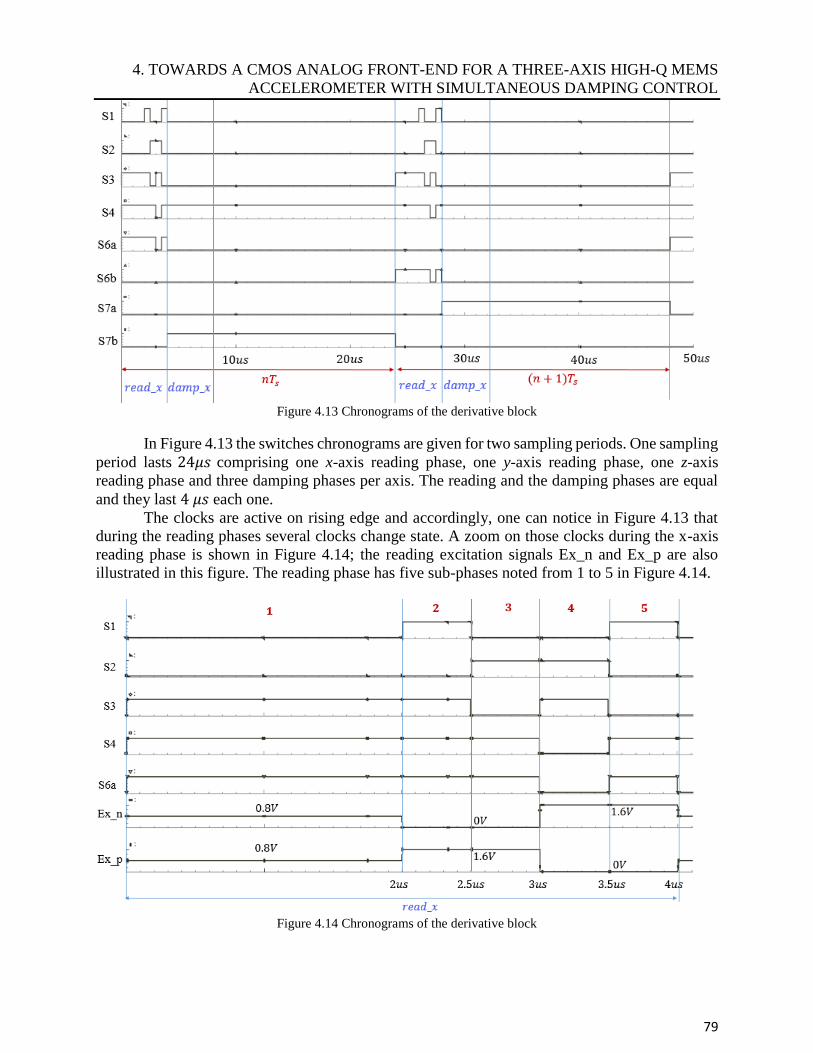
4. TOWARDS A CMOS ANALOG FRONT-END FOR A THREE-AXIS HIGH-Q MEMS
ACCELEROMETER WITH SIMULTANEOUS DAMPING CONTROL
79
Figure 4.13 Chronograms of the derivative block
In Figure 4.13 the switches chronograms are given for two sampling periods. One sampling
period lasts 24𝜇𝑠 comprising one x-axis reading phase, one y-axis reading phase, one z-axis
reading phase and three damping phases per axis. The reading and the damping phases are equal
and they last 4 𝜇𝑠 each one.
The clocks are active on rising edge and accordingly, one can notice in Figure 4.13 that
during the reading phases several clocks change state. A zoom on those clocks during the x-axis
reading phase is shown in Figure 4.14; the reading excitation signals Ex_n and Ex_p are also
illustrated in this figure. The reading phase has five sub-phases noted from 1 to 5 in Figure 4.14.
Figure 4.14 Chronograms of the derivative block
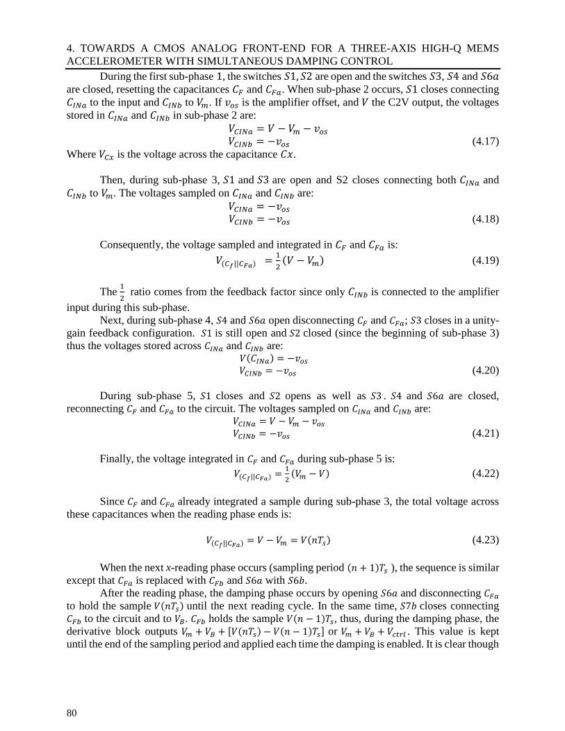
4. TOWARDS A CMOS ANALOG FRONT-END FOR A THREE-AXIS HIGH-Q MEMS
ACCELEROMETER WITH SIMULTANEOUS DAMPING CONTROL
80
During the first sub-phase 1, the switches 𝑆1, 𝑆2 are open and the switches 𝑆3, 𝑆4 and 𝑆6𝑎
are closed, resetting the capacitances 𝐶𝐹 and 𝐶𝐹𝑎. When sub-phase 2 occurs, 𝑆1 closes connecting
𝐶𝐼𝑁𝑎 to the input and 𝐶𝐼𝑁𝑏 to 𝑉𝑚. If 𝑣𝑜𝑠 is the amplifier offset, and 𝑉 the C2V output, the voltages
stored in 𝐶𝐼𝑁𝑎 and 𝐶𝐼𝑁𝑏 in sub-phase 2 are:
𝑉𝐶𝐼𝑁𝑎 = 𝑉 − 𝑉𝑚 − 𝑣𝑜𝑠 𝑉𝐶𝐼𝑁𝑏 = −𝑣𝑜𝑠 (4.17)
Where 𝑉𝐶𝑥 is the voltage across the capacitance 𝐶𝑥.
Then, during sub-phase 3, 𝑆1 and 𝑆3 are open and S2 closes connecting both 𝐶𝐼𝑁𝑎 and
𝐶𝐼𝑁𝑏 to 𝑉𝑚. The voltages sampled on 𝐶𝐼𝑁𝑎 and 𝐶𝐼𝑁𝑏 are:
𝑉𝐶𝐼𝑁𝑎 = −𝑣𝑜𝑠 𝑉𝐶𝐼𝑁𝑏 = −𝑣𝑜𝑠 (4.18)
Consequently, the voltage sampled and integrated in 𝐶𝐹 and 𝐶𝐹𝑎 is:
𝑉(𝐶𝑓||𝐶𝐹𝑎) =1
2(𝑉 − 𝑉𝑚) (4.19)
The 1
2 ratio comes from the feedback factor since only 𝐶𝐼𝑁𝑏 is connected to the amplifier
input during this sub-phase.
Next, during sub-phase 4, 𝑆4 and 𝑆6𝑎 open disconnecting 𝐶𝐹 and 𝐶𝐹𝑎; 𝑆3 closes in a unity-
gain feedback configuration. 𝑆1 is still open and 𝑆2 closed (since the beginning of sub-phase 3)
thus the voltages stored across 𝐶𝐼𝑁𝑎 and 𝐶𝐼𝑁𝑏 are: 𝑉(𝐶𝐼𝑁𝑎) = −𝑣𝑜𝑠
𝑉𝐶𝐼𝑁𝑏 = −𝑣𝑜𝑠 (4.20)
During sub-phase 5, 𝑆1 closes and 𝑆2 opens as well as 𝑆3 . 𝑆4 and 𝑆6𝑎 are closed,
reconnecting 𝐶𝐹 and 𝐶𝐹𝑎 to the circuit. The voltages sampled on 𝐶𝐼𝑁𝑎 and 𝐶𝐼𝑁𝑏 are: 𝑉𝐶𝐼𝑁𝑎 = 𝑉 − 𝑉𝑚 − 𝑣𝑜𝑠 𝑉𝐶𝐼𝑁𝑏 = −𝑣𝑜𝑠 (4.21)
Finally, the voltage integrated in 𝐶𝐹 and 𝐶𝐹𝑎 during sub-phase 5 is:
𝑉(𝐶𝑓||𝐶𝐹𝑎) =1
2(𝑉𝑚 − 𝑉) (4.22)
Since 𝐶𝐹 and 𝐶𝐹𝑎 already integrated a sample during sub-phase 3, the total voltage across
these capacitances when the reading phase ends is:
𝑉(𝐶𝑓||𝐶𝐹𝑎) = 𝑉 − 𝑉𝑚 = 𝑉(𝑛𝑇𝑠) (4.23)
When the next x-reading phase occurs (sampling period (𝑛 + 1)𝑇𝑠 ), the sequence is similar
except that 𝐶𝐹𝑎 is replaced with 𝐶𝐹𝑏 and 𝑆6𝑎 with 𝑆6𝑏.
After the reading phase, the damping phase occurs by opening 𝑆6𝑎 and disconnecting 𝐶𝐹𝑎
to hold the sample 𝑉(𝑛𝑇𝑠) until the next reading cycle. In the same time, 𝑆7𝑏 closes connecting
𝐶𝐹𝑏 to the circuit and to 𝑉𝐵. 𝐶𝐹𝑏 holds the sample 𝑉(𝑛 − 1)𝑇𝑠, thus, during the damping phase, the
derivative block outputs 𝑉𝑚 + 𝑉𝐵 + [𝑉(𝑛𝑇𝑠) − 𝑉(𝑛 − 1)𝑇𝑠] or 𝑉𝑚 + 𝑉𝐵 + 𝑉𝑐𝑡𝑟𝑙 . This value is kept
until the end of the sampling period and applied each time the damping is enabled. It is clear though
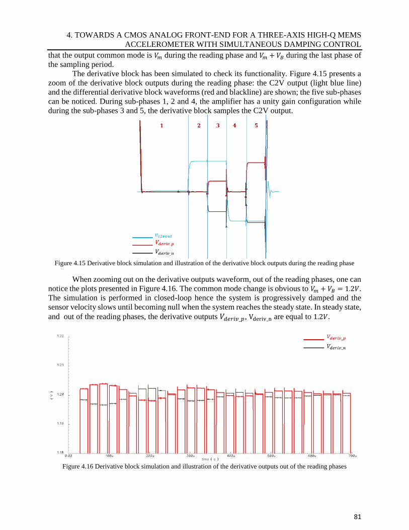
4. TOWARDS A CMOS ANALOG FRONT-END FOR A THREE-AXIS HIGH-Q MEMS
ACCELEROMETER WITH SIMULTANEOUS DAMPING CONTROL
81
that the output common mode is 𝑉𝑚 during the reading phase and 𝑉𝑚 + 𝑉𝐵 during the last phase of
the sampling period.
The derivative block has been simulated to check its functionality. Figure 4.15 presents a
zoom of the derivative block outputs during the reading phase: the C2V output (light blue line)
and the differential derivative block waveforms (red and blackline) are shown; the five sub-phases
can be noticed. During sub-phases 1, 2 and 4, the amplifier has a unity gain configuration while
during the sub-phases 3 and 5, the derivative block samples the C2V output.
Figure 4.15 Derivative block simulation and illustration of the derivative block outputs during the reading phase
When zooming out on the derivative outputs waveform, out of the reading phases, one can
notice the plots presented in Figure 4.16. The common mode change is obvious to 𝑉𝑚 + 𝑉𝐵 = 1.2𝑉.
The simulation is performed in closed-loop hence the system is progressively damped and the
sensor velocity slows until becoming null when the system reaches the steady state. In steady state,
and out of the reading phases, the derivative outputs 𝑉𝑑𝑒𝑟𝑖𝑣_𝑝, Vderiv_n are equal to 1.2𝑉.
Figure 4.16 Derivative block simulation and illustration of the derivative outputs out of the reading phases
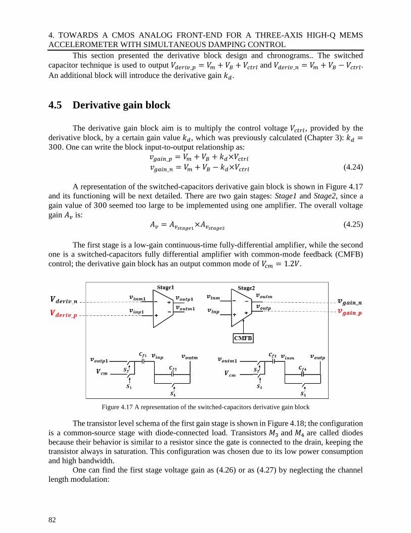
4. TOWARDS A CMOS ANALOG FRONT-END FOR A THREE-AXIS HIGH-Q MEMS
ACCELEROMETER WITH SIMULTANEOUS DAMPING CONTROL
82
This section presented the derivative block design and chronograms.. The switched
capacitor technique is used to output 𝑉𝑑𝑒𝑟𝑖𝑣_𝑝 = 𝑉𝑚 + 𝑉𝐵 + 𝑉𝑐𝑡𝑟𝑙 and 𝑉𝑑𝑒𝑟𝑖𝑣_𝑛 = 𝑉𝑚 + 𝑉𝐵 − 𝑉𝑐𝑡𝑟𝑙.
An additional block will introduce the derivative gain 𝑘𝑑.
4.5 Derivative gain block
The derivative gain block aim is to multiply the control voltage 𝑉𝑐𝑡𝑟𝑙 , provided by the
derivative block, by a certain gain value 𝑘𝑑, which was previously calculated (Chapter 3): 𝑘𝑑 =300. One can write the block input-to-output relationship as:
𝑣𝑔𝑎𝑖𝑛_𝑝 = 𝑉𝑚 + 𝑉𝐵 + 𝑘𝑑×𝑉𝑐𝑡𝑟𝑙
𝑣𝑔𝑎𝑖𝑛_𝑛 = 𝑉𝑚 + 𝑉𝐵 − 𝑘𝑑×𝑉𝑐𝑡𝑟𝑙 (4.24)
A representation of the switched-capacitors derivative gain block is shown in Figure 4.17
and its functioning will be next detailed. There are two gain stages: Stage1 and Stage2, since a
gain value of 300 seemed too large to be implemented using one amplifier. The overall voltage
gain 𝐴𝑣 is:
𝐴𝑣 = 𝐴𝑣𝑠𝑡𝑎𝑔𝑒1×𝐴𝑣𝑠𝑡𝑎𝑔𝑒2
(4.25)
The first stage is a low-gain continuous-time fully-differential amplifier, while the second
one is a switched-capacitors fully differential amplifier with common-mode feedback (CMFB)
control; the derivative gain block has an output common mode of 𝑉𝑐𝑚 = 1.2𝑉.
Figure 4.17 A representation of the switched-capacitors derivative gain block
The transistor level schema of the first gain stage is shown in Figure 4.18; the configuration
is a common-source stage with diode-connected load. Transistors 𝑀3 and 𝑀4 are called diodes
because their behavior is similar to a resistor since the gate is connected to the drain, keeping the
transistor always in saturation. This configuration was chosen due to its low power consumption
and high bandwidth.
One can find the first stage voltage gain as (4.26) or as (4.27) by neglecting the channel
length modulation:
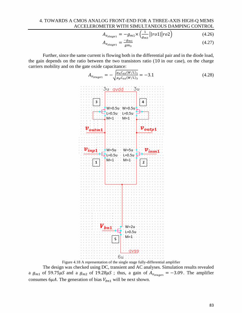
4. TOWARDS A CMOS ANALOG FRONT-END FOR A THREE-AXIS HIGH-Q MEMS
ACCELEROMETER WITH SIMULTANEOUS DAMPING CONTROL
83
𝐴𝑣𝑠𝑡𝑎𝑔𝑒1= −𝑔𝑚1× (
1
𝑔𝑚3||𝑟𝑜1||𝑟𝑜2) (4.26)
𝐴𝑣𝑠𝑡𝑎𝑔𝑒1=
−𝑔𝑚1
𝑔𝑚3 (4.27)
Further, since the same current is flowing both in the differential pair and in the diode load,
the gain depends on the ratio between the two transistors ratio (10 in our case), on the charge
carriers mobility and on the gate oxide capacitance:
𝐴𝑣𝑠𝑡𝑎𝑔𝑒1= −√
𝜇𝑛𝐶𝑜𝑥(𝑊 𝐿⁄ )1
𝜇𝑝𝐶𝑜𝑥(𝑊 𝐿⁄ )3= −3.1 (4.28)
Figure 4.18 A representation of the single stage fully-differential amplifier
The design was checked using DC, transient and AC analyses. Simulation results revealed
a 𝑔𝑚1 of 59.75𝜇𝑆 and a 𝑔𝑚2 of 19.28𝜇𝑆 ; thus, a gain of 𝐴𝑣𝑠𝑡𝑎𝑔𝑒1= −3.09 . The amplifier
consumes 6𝜇𝐴. The generation of bias 𝑉𝑏𝑛1 will be next shown.
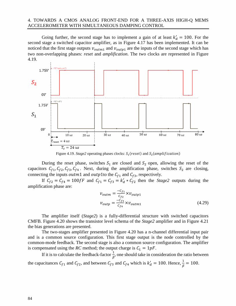
4. TOWARDS A CMOS ANALOG FRONT-END FOR A THREE-AXIS HIGH-Q MEMS
ACCELEROMETER WITH SIMULTANEOUS DAMPING CONTROL
84
Going further, the second stage has to implement a gain of at least 𝑘𝑑′ = 100. For the
second stage a switched capacitor amplifier, as in Figure 4.17 has been implemented. It can be
noticed that the first stage outputs 𝑣𝑜𝑢𝑡𝑚1 and 𝑣𝑜𝑢𝑡𝑝1 are the inputs of the second stage which has
two non-overlapping phases: reset and amplification. The two clocks are represented in Figure
4.19.
Figure 4.19. Stage2 operating phases clocks: 𝑆1(𝑟𝑒𝑠𝑒𝑡) and 𝑆2(𝑎𝑚𝑝𝑙𝑖𝑓𝑖𝑐𝑎𝑡𝑖𝑜𝑛)
During the reset phase, switches 𝑆1 are closed and 𝑆2 open, allowing the reset of the
capacitors 𝐶𝑓1, 𝐶𝑓2, 𝐶𝑓3, 𝐶𝑓4 . Next, during the amplification phase, switches 𝑆2 are closing,
connecting the inputs 𝑜𝑢𝑡𝑚1 and 𝑜𝑢𝑡𝑝1to the 𝐶𝑓1 and 𝐶𝑓3, respectively.
If 𝐶𝑓2 = 𝐶𝑓4 = 100𝑓𝐹 and 𝐶𝑓1 = 𝐶𝑓3 = 𝑘𝑑′ ∗ 𝐶𝑓2 then the Stage2 outputs during the
amplification phase are:
𝑣𝑜𝑢𝑡𝑚 =−𝐶𝑓1
𝐶𝑓2×𝑣𝑜𝑢𝑡𝑝1
𝑣𝑜𝑢𝑡𝑝 =−𝐶𝑓3
𝐶𝑓4×𝑣𝑜𝑢𝑡𝑚1 (4.29)
The amplifier itself (Stage2) is a fully-differential structure with switched capacitors
CMFB. Figure 4.20 shows the transistor level schema of the Stage2 amplifier and in Figure 4.21
the bias generations are presented.
The two-stages amplifier presented in Figure 4.20 has a n-channel differential input pair
and is a common source configuration. This first stage output is the node controlled by the
common-mode feedback. The second stage is also a common source configuration. The amplifier
is compensated using the RC method; the output charge is 𝐶𝐿 = 1𝑝𝐹.
If it is to calculate the feedback-factor 1
𝛽, one should take in consideration the ratio between
the capacitances 𝐶𝑓1 and 𝐶𝑓2, and between 𝐶𝑓3 and 𝐶𝑓4 which is 𝑘𝑑′ = 100. Hence,
1
𝛽= 100.
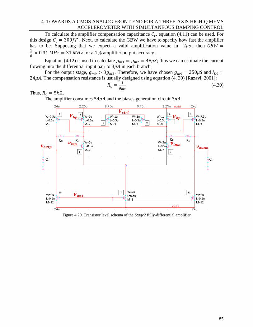
4. TOWARDS A CMOS ANALOG FRONT-END FOR A THREE-AXIS HIGH-Q MEMS
ACCELEROMETER WITH SIMULTANEOUS DAMPING CONTROL
85
To calculate the amplifier compensation capacitance 𝐶𝑐, equation (4.11) can be used. For
this design 𝐶𝑐 = 300𝑓𝐹 . Next, to calculate the GBW we have to specify how fast the amplifier
has to be. Supposing that we expect a valid amplification value in 2𝜇𝑠 , then 𝐺𝐵𝑊 =1
𝛽 × 0.31 𝑀𝐻𝑧 = 31 𝑀𝐻𝑧 for a 1% amplifier output accuracy.
Equation (4.12) is used to calculate 𝑔𝑚1 = 𝑔𝑚2 = 48𝜇𝑆; thus we can estimate the current
flowing into the differential input pair to 3𝜇𝐴 in each branch.
For the output stage, 𝑔𝑚9 > 3𝑔𝑚2. Therefore, we have chosen 𝑔𝑚9 = 250𝜇𝑆 and 𝐼𝐷9 =24𝜇𝐴. The compensation resistance is usually designed using equation (4. 30) [Razavi, 2001]:
𝑅𝑐 =1
𝑔𝑚9 (4.30)
Thus, 𝑅𝑐 = 5𝑘Ω.
The amplifier consumes 54𝜇𝐴 and the biases generation circuit 3𝜇𝐴.
Figure 4.20. Transistor level schema of the Stage2 fully-differential amplifier
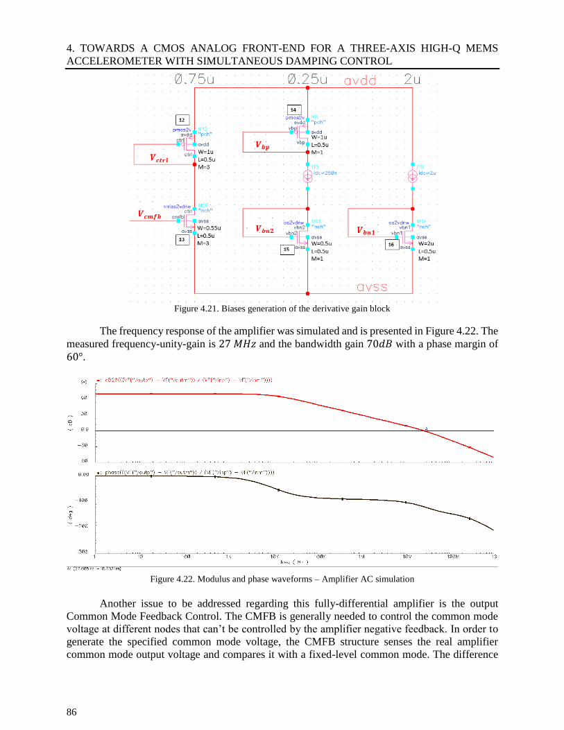
4. TOWARDS A CMOS ANALOG FRONT-END FOR A THREE-AXIS HIGH-Q MEMS
ACCELEROMETER WITH SIMULTANEOUS DAMPING CONTROL
86
Figure 4.21. Biases generation of the derivative gain block
The frequency response of the amplifier was simulated and is presented in Figure 4.22. The
measured frequency-unity-gain is 27 𝑀𝐻𝑧 and the bandwidth gain 70𝑑𝐵 with a phase margin of
60°.
Figure 4.22. Modulus and phase waveforms – Amplifier AC simulation
Another issue to be addressed regarding this fully-differential amplifier is the output
Common Mode Feedback Control. The CMFB is generally needed to control the common mode
voltage at different nodes that can’t be controlled by the amplifier negative feedback. In order to
generate the specified common mode voltage, the CMFB structure senses the real amplifier
common mode output voltage and compares it with a fixed-level common mode. The difference
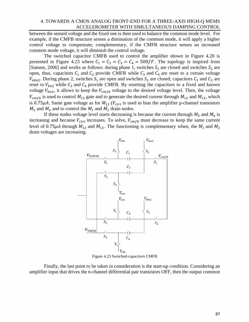
4. TOWARDS A CMOS ANALOG FRONT-END FOR A THREE-AXIS HIGH-Q MEMS
ACCELEROMETER WITH SIMULTANEOUS DAMPING CONTROL
87
between the sensed voltage and the fixed one is then used to balance the common mode level. For
example, if the CMFB structure senses a diminution of the common mode, it will apply a higher
control voltage to compensate; complementary, if the CMFB structure senses an increased
common mode voltage, it will diminish the control voltage. The switched capacitor CMFB used to control the amplifier shown in Figure 4.20 is
presented in Figure 4.23 where 𝐶1 = 𝐶2 = 𝐶3 = 𝐶4 = 500𝑓𝐹 . The topology is inspired from
[Sansen, 2006] and works as follows: during phase 1, switches 𝑆1 are closed and switches 𝑆2 are
open, thus, capacitors 𝐶1 and 𝐶2 provide CMFB while 𝐶3 and 𝐶4 are reset to a certain voltage
𝑉𝑣𝑏𝑛2. During phase 2, switches 𝑆1 are open and switches 𝑆2 are closed; capacitors 𝐶1 and 𝐶2 are
reset to 𝑉𝑏𝑛2 while 𝐶3 and 𝐶4 provide CMFB. By resetting the capacitors to a fixed and known
voltage 𝑉𝑏𝑛2, it allows to keep the 𝑉𝑐𝑚𝑓𝑏 voltage to the desired voltage level. Then, the voltage
𝑉𝑐𝑚𝑓𝑏 is used to control 𝑀13 gate and to generate the desired current through 𝑀12 and 𝑀13, which
is 0.75𝜇𝐴. Same gate voltage as for 𝑀12 (𝑉𝑐𝑡𝑟𝑙 is used to bias the amplifier p-channel transistors
𝑀5 and 𝑀6 and to control the 𝑀1 and 𝑀2 drain nodes.
If these nodes voltage level starts decreasing is because the current through 𝑀5 and 𝑀6 is
increasing and because 𝑉𝑐𝑡𝑟𝑙 increases. To solve, 𝑉𝑐𝑚𝑓𝑏 must decrease to keep the same current
level of 0.75𝜇𝐴 through 𝑀12 and 𝑀13. The functioning is complementary when, the 𝑀1 and 𝑀2
drain voltages are increasing.
Figure 4.23 Switched-capacitors CMFB
Finally, the last point to be taken in consideration is the start-up condition. Considering an
amplifier input that drives the n-channel differential pair transistors OFF, then the output common
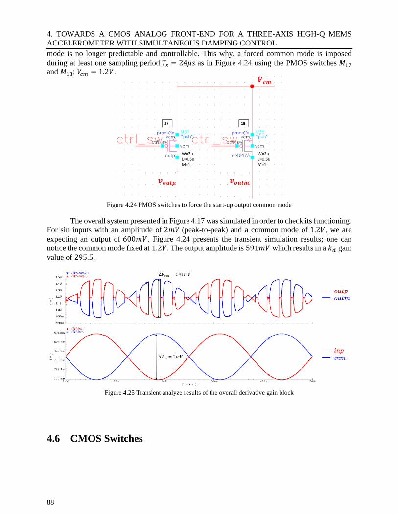
4. TOWARDS A CMOS ANALOG FRONT-END FOR A THREE-AXIS HIGH-Q MEMS
ACCELEROMETER WITH SIMULTANEOUS DAMPING CONTROL
88
mode is no longer predictable and controllable. This why, a forced common mode is imposed
during at least one sampling period 𝑇𝑠 = 24𝜇𝑠 as in Figure 4.24 using the PMOS switches 𝑀17
and 𝑀18; 𝑉𝑐𝑚 = 1.2𝑉.
Figure 4.24 PMOS switches to force the start-up output common mode
The overall system presented in Figure 4.17 was simulated in order to check its functioning.
For sin inputs with an amplitude of 2𝑚𝑉 (peak-to-peak) and a common mode of 1.2𝑉, we are
expecting an output of 600𝑚𝑉 . Figure 4.24 presents the transient simulation results; one can
notice the common mode fixed at 1.2𝑉. The output amplitude is 591𝑚𝑉 which results in a 𝑘𝑑 gain
value of 295.5.
Figure 4.25 Transient analyze results of the overall derivative gain block
4.6 CMOS Switches
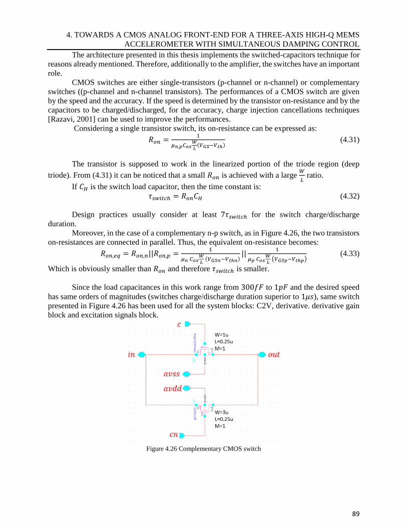
4. TOWARDS A CMOS ANALOG FRONT-END FOR A THREE-AXIS HIGH-Q MEMS
ACCELEROMETER WITH SIMULTANEOUS DAMPING CONTROL
89
The architecture presented in this thesis implements the switched-capacitors technique for
reasons already mentioned. Therefore, additionally to the amplifier, the switches have an important
role.
CMOS switches are either single-transistors (p-channel or n-channel) or complementary
switches ((p-channel and n-channel transistors). The performances of a CMOS switch are given
by the speed and the accuracy. If the speed is determined by the transistor on-resistance and by the
capacitors to be charged/discharged, for the accuracy, charge injection cancellations techniques
[Razavi, 2001] can be used to improve the performances.
Considering a single transistor switch, its on-resistance can be expressed as:
𝑅𝑜𝑛 =1
𝜇𝑛,𝑝𝐶𝑜𝑥𝑊
𝐿(𝑉𝐺𝑆−𝑉𝑡ℎ)
(4.31)
The transistor is supposed to work in the linearized portion of the triode region (deep
triode). From (4.31) it can be noticed that a small 𝑅𝑜𝑛 is achieved with a large 𝑊
𝐿 ratio.
If 𝐶𝐻 is the switch load capacitor, then the time constant is:
𝜏𝑠𝑤𝑖𝑡𝑐ℎ = 𝑅𝑜𝑛𝐶𝐻 (4.32)
Design practices usually consider at least 7𝜏𝑠𝑤𝑖𝑡𝑐ℎ for the switch charge/discharge
duration.
Moreover, in the case of a complementary n-p switch, as in Figure 4.26, the two transistors
on-resistances are connected in parallel. Thus, the equivalent on-resistance becomes:
𝑅𝑜𝑛,𝑒𝑞 = 𝑅𝑜𝑛,𝑛||𝑅𝑜𝑛,𝑝 =1
𝜇𝑛 𝐶𝑜𝑥𝑊
𝐿 (𝑉𝐺𝑆𝑛−𝑉𝑡ℎ𝑛)
||1
𝜇𝑝 𝐶𝑜𝑥𝑊
𝐿 (𝑉𝐺𝑆𝑝−𝑉𝑡ℎ𝑝)
(4.33)
Which is obviously smaller than 𝑅𝑜𝑛 and therefore 𝜏𝑠𝑤𝑖𝑡𝑐ℎ is smaller.
Since the load capacitances in this work range from 300𝑓𝐹 to 1𝑝𝐹 and the desired speed
has same orders of magnitudes (switches charge/discharge duration superior to 1𝜇𝑠), same switch
presented in Figure 4.26 has been used for all the system blocks: C2V, derivative. derivative gain
block and excitation signals block.
Figure 4.26 Complementary CMOS switch
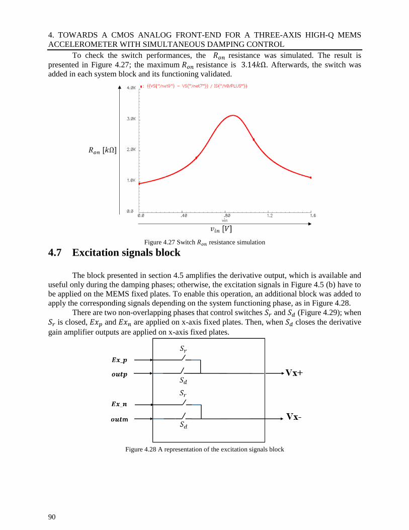
4. TOWARDS A CMOS ANALOG FRONT-END FOR A THREE-AXIS HIGH-Q MEMS
ACCELEROMETER WITH SIMULTANEOUS DAMPING CONTROL
90
To check the switch performances, the 𝑅𝑜𝑛 resistance was simulated. The result is
presented in Figure 4.27; the maximum 𝑅𝑜𝑛 resistance is 3.14𝑘Ω. Afterwards, the switch was
added in each system block and its functioning validated.
Figure 4.27 Switch 𝑅𝑜𝑛 resistance simulation
4.7 Excitation signals block
The block presented in section 4.5 amplifies the derivative output, which is available and
useful only during the damping phases; otherwise, the excitation signals in Figure 4.5 (b) have to
be applied on the MEMS fixed plates. To enable this operation, an additional block was added to
apply the corresponding signals depending on the system functioning phase, as in Figure 4.28.
There are two non-overlapping phases that control switches 𝑆𝑟 and 𝑆𝑑 (Figure 4.29); when
𝑆𝑟 is closed, 𝐸𝑥𝑝 and 𝐸𝑥𝑛 are applied on x-axis fixed plates. Then, when 𝑆𝑑 closes the derivative
gain amplifier outputs are applied on x-axis fixed plates.
Figure 4.28 A representation of the excitation signals block
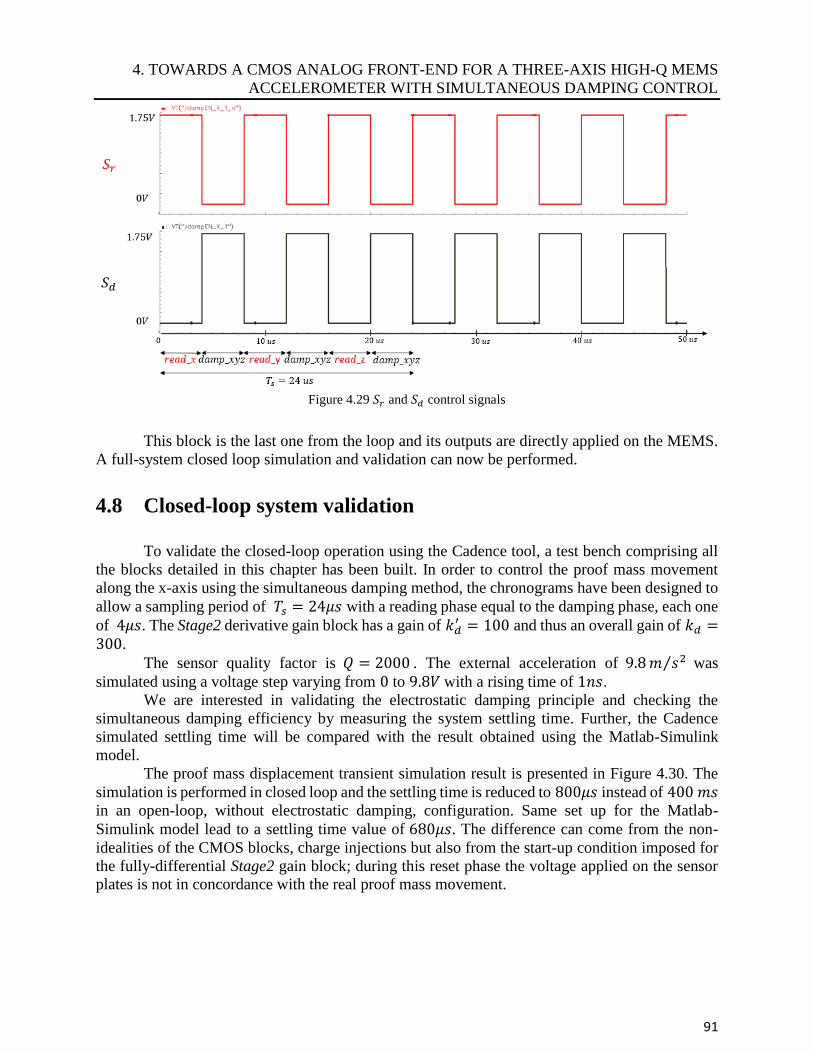
4. TOWARDS A CMOS ANALOG FRONT-END FOR A THREE-AXIS HIGH-Q MEMS
ACCELEROMETER WITH SIMULTANEOUS DAMPING CONTROL
91
Figure 4.29 𝑆𝑟 and 𝑆𝑑 control signals
This block is the last one from the loop and its outputs are directly applied on the MEMS.
A full-system closed loop simulation and validation can now be performed.
4.8 Closed-loop system validation
To validate the closed-loop operation using the Cadence tool, a test bench comprising all
the blocks detailed in this chapter has been built. In order to control the proof mass movement
along the x-axis using the simultaneous damping method, the chronograms have been designed to
allow a sampling period of 𝑇𝑠 = 24𝜇𝑠 with a reading phase equal to the damping phase, each one
of 4𝜇𝑠. The Stage2 derivative gain block has a gain of 𝑘𝑑′ = 100 and thus an overall gain of 𝑘𝑑 =
300.
The sensor quality factor is 𝑄 = 2000 . The external acceleration of 9.8 𝑚 𝑠2⁄ was
simulated using a voltage step varying from 0 to 9.8𝑉 with a rising time of 1𝑛𝑠.
We are interested in validating the electrostatic damping principle and checking the
simultaneous damping efficiency by measuring the system settling time. Further, the Cadence
simulated settling time will be compared with the result obtained using the Matlab-Simulink
model.
The proof mass displacement transient simulation result is presented in Figure 4.30. The
simulation is performed in closed loop and the settling time is reduced to 800𝜇𝑠 instead of 400 𝑚𝑠
in an open-loop, without electrostatic damping, configuration. Same set up for the Matlab-
Simulink model lead to a settling time value of 680𝜇𝑠. The difference can come from the non-
idealities of the CMOS blocks, charge injections but also from the start-up condition imposed for
the fully-differential Stage2 gain block; during this reset phase the voltage applied on the sensor
plates is not in concordance with the real proof mass movement.
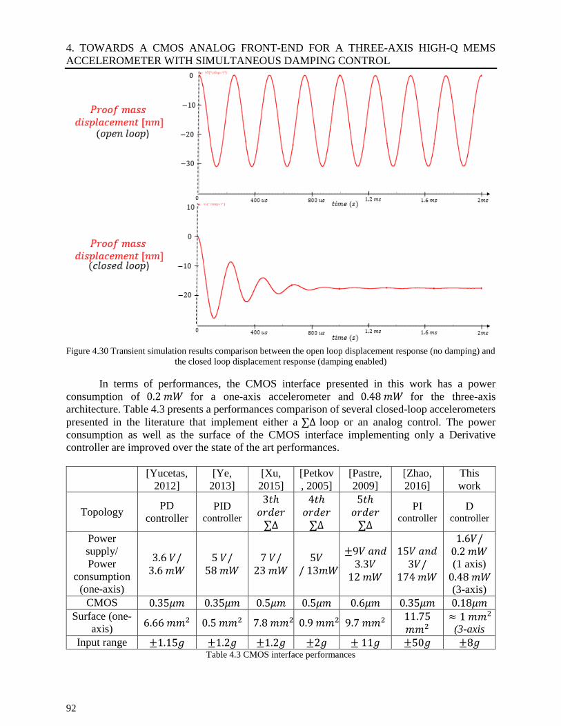
4. TOWARDS A CMOS ANALOG FRONT-END FOR A THREE-AXIS HIGH-Q MEMS
ACCELEROMETER WITH SIMULTANEOUS DAMPING CONTROL
92
Figure 4.30 Transient simulation results comparison between the open loop displacement response (no damping) and
the closed loop displacement response (damping enabled)
In terms of performances, the CMOS interface presented in this work has a power
consumption of 0.2 𝑚𝑊 for a one-axis accelerometer and 0.48 𝑚𝑊 for the three-axis
architecture. Table 4.3 presents a performances comparison of several closed-loop accelerometers
presented in the literature that implement either a ∑∆ loop or an analog control. The power
consumption as well as the surface of the CMOS interface implementing only a Derivative
controller are improved over the state of the art performances.
[Yucetas,
2012]
[Ye,
2013]
[Xu,
2015]
[Petkov
, 2005]
[Pastre,
2009]
[Zhao,
2016]
This
work
Topology PD
controller PID
controller
3𝑡ℎ
𝑜𝑟𝑑𝑒𝑟
∑∆
4𝑡ℎ
𝑜𝑟𝑑𝑒𝑟
∑∆
5𝑡ℎ
𝑜𝑟𝑑𝑒𝑟
∑∆
PI controller
D controller
Power
supply/
Power
consumption
(one-axis)
3.6 𝑉/
3.6 𝑚𝑊
5 𝑉/
58 𝑚𝑊
7 𝑉/
23 𝑚𝑊
5𝑉/ 13𝑚𝑊
±9𝑉 𝑎𝑛𝑑
3.3𝑉
12 𝑚𝑊
15𝑉 𝑎𝑛𝑑
3𝑉/
174 𝑚𝑊
1.6𝑉/
0.2 𝑚𝑊 (1 axis)
0.48 𝑚𝑊 (3-axis)
CMOS 0.35𝜇𝑚 0.35𝜇𝑚 0.5𝜇𝑚 0.5𝜇𝑚 0.6𝜇𝑚 0.35𝜇𝑚 0.18𝜇𝑚
Surface (one-
axis) 6.66 𝑚𝑚2 0.5 𝑚𝑚2 7.8 𝑚𝑚2 0.9 𝑚𝑚2 9.7 𝑚𝑚2
11.75
𝑚𝑚2
≈ 1 𝑚𝑚2 (3-axis
Input range ±1.15𝑔 ±1.2𝑔 ±1.2𝑔 ±2𝑔 ± 11𝑔 ±50𝑔 ±8𝑔 Table 4.3 CMOS interface performances
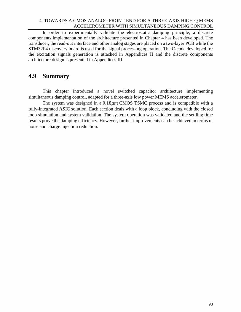
4. TOWARDS A CMOS ANALOG FRONT-END FOR A THREE-AXIS HIGH-Q MEMS
ACCELEROMETER WITH SIMULTANEOUS DAMPING CONTROL
93
In order to experimentally validate the electrostatic damping principle, a discrete
components implementation of the architecture presented in Chapter 4 has been developed. The
transducer, the read-out interface and other analog stages are placed on a two-layer PCB while the
STM32F4 discovery board is used for the signal processing operation. The C-code developed for
the excitation signals generation is attached in Appendices II and the discrete components
architecture design is presented in Appendices III.
4.9 Summary
This chapter introduced a novel switched capacitor architecture implementing
simultaneous damping control, adapted for a three-axis low power MEMS accelerometer.
The system was designed in a 0.18𝜇𝑚 CMOS TSMC process and is compatible with a
fully-integrated ASIC solution. Each section deals with a loop block, concluding with the closed
loop simulation and system validation. The system operation was validated and the settling time
results prove the damping efficiency. However, further improvements can be achieved in terms of
noise and charge injection reduction.

4. TOWARDS A CMOS ANALOG FRONT-END FOR A THREE-AXIS HIGH-Q MEMS
ACCELEROMETER WITH SIMULTANEOUS DAMPING CONTROL
94
95
Conclusions and perspectives
Recently, consumer electronics industry has known a spectacular growth that would have
not been possible without pushing the integration barrier further and further. In this context,
MEMS have known an exponential growth and are, nowadays, embedded in most consumer
applications. In addition, sensing multiple DoF with a unique integrated circuit has become the
new trend in the Internet of Things era since both power and cost reductions are the keys of this
continuously developing industry.
Capacitive MEMS inertial sensors, as the accelerometers and the gyroscopes, have won
their places in consumer electronics and are currently subject to various research topics. Here, the
accelerometer-gyroscope fusion research topic has been addressed and this thesis had as main
objective the design of the analog front-end circuits to drive and sense an underdamped three-axis
accelerometer efficiently.
Firstly, the issue related to the native underdamped architecture of the accelerometer, has
been stated: long transducer settling time and weak control over the sensor behavior. Several
control methods have been investigated and the proposed architecture choice has been designed
and optimized to suit the MEMS designed by NXP Semiconductors. The transducer is here a dual-
mass three-axis capacitive accelerometer, the proof mass of which is common to the three axes.
Consequently, an acceleration measurement along the three axes can be only performed
sequentially.
The analog control which implements electrostatic damping for this system, is based on
the linear relationship between the net electrostatic force and the proof mass velocity estimation.
As far as the acceleration measurement itself is concerned, the damping should be applied
sequentially to not perturb different axes operation.
The main goal of the thesis is the design of an analog control architecture achieving low
power consumption. In this context, the novel system proposed in this work has as main features
the analog first stage shared among the three axes, the switched-capacitor technique used in the
main loop blocks but also the analog blocks operation under a low power supply. Furthermore, no
additional charge-pump block or high voltage CMOS process are required for a successful
damping control. Finally, the thesis presents the development of a new damping chronogram
(simultaneous damping) which improves the damping efficiency compared to the state of the art
damping methodology (successive damping).
The simultaneous damping technique is based on the artificial damping generation starting
from the proof mass velocity estimation and on sampling, holding and applying this very same
damping value three times within the same sampling frequency. The mathematical modeling of
the simultaneous damping technique has been very challenging since the overall discrete closed-
loop transfer function couldn’t be developed using the classical z-transform method. The
simultaneous damping requires at least two different operating sampling frequencies and thus,
provides a multirate control over the MEMS behavior. Using down sampling and up sampling
signal processing techniques, a mathematical model that develops the multirate controller
properties has been designed to give more insight in the loop stability and provide a mean to assess
CONCLUSIONS AND PERSPECTIVES
96
the impact of the sampling frequency and gain of the loop on its stability. Using this method
together with the model, the sampling frequency and the loop gain value have been determined for
the CMOS implementation.
The thesis describes also each block modeling (Matlab-Simulink) and the closed loop
simulations along with the concept validation. For the transducer, the read-out interface and the
control block (derivative), several behavioral models have been developed and the settling time
method has been used to assess the damping efficiency. Finally, the simultaneous damping
architecture has been implemented in this work due to its higher performances in term of settling
time.
The transistor-level design of the accelerometer signal chain is based on switched-capacitor
techniques and can be further integrated within an ASIC. The design operation as well as the
damping efficiency have been validated using Cadence Spectre simulations. Lastly, a discrete
components architecture has been designed to experimentally validate the simultaneous damping
concept.
In perspective, a fully ASIC design together with the microfabrication and the
characterization is necessary to experimentally validate the integrated circuit solution. To do so,
already available analog blocks such as the bandgap or the oscillator can be used; however,
additional digital design is required to conceive the CMOS logic used to control the analog
operation. Finally, ASIC top cell verification must be performed to validate both analog and digital
operation.
Going further, a fully-differential (using both transducer masses) system solution can be
imagined. Since the two masses are oppositely moving under the effect of same acceleration value
and the fixed electrodes are shared between the two masses, the control voltage can no longer be
applied on the fixed excitation plates. Otherwise, it will cause the desired damping effect for one
of the proof masses but will drive the other mass even more instable. Two solutions can be
imagined to solve these issues: firstly, the transducer fixed electrodes can be separated (one for
each proof mass) if a MEMS design review is possible. In this way, different electrostatic forces
can be applied on each mass and both can be controlled. Secondly, the bias voltage 𝑉𝐵 can be
differentially applied on the proof masses during the damping phase and the damping effect will
be in concordance with each mass motion as a result. However, another issue that may arise, is the
electrostatic forces apparition between the sensor shield and the masses, which can perturb the
operation. The MEMS Verilog-A Spectre model can be adjusted in order to take into account the
phenomenon and to validate this possible implementation. In addition, design improvements in
terms of noise and charge injections can be further achieved by employing low-noise and charge
injection reduction techniques.
In conclusion, the thesis presented a novel simultaneous damping architecture adapted for
a three-axis capacitive transducer, that considerably reduces the settling time compared with the
state of the art approach (2 times smaller, for a sampling time of 24 𝜇𝑠 ) and 500 times smaller
compared with an open loop operation. The system stability can now be studied using a new
method that certifies the closed loop stability for a certain sampling time and loop gain value.
Transistor-level design validated the overall mathematical and behavioral modeling.
97
Bibliography
1. [Aaltonen, 2007] – L. Aaltonen, P. Rahikkala, M. Saukoski, K. Halonen “Continuous Time
Interface for ± 1.5 g Closed-Loop Accelerometer” IEEE International Conference on
Integrated Circuit Design and Technology, September 2007.
2. [Allen, 2009] – J. Allen “Micro-System Inertial Sensing Technology Overview” Sandia
National Laboratories, April 2009.
3. [Allen, Holberg, 2002] - Phillip E. Allen, Douglas R. Holberg “CMOS Analog Circuit
Design”, Oxford University Press, 2002.
4. [Amini, 2004] - B. Amini, F. Ayazi, “A 2.5-V 14-bit ΣΔ CMOS SOI capacitive
accelerometer,” IEEE Journal of Solid-State Circuits, vol. 39, pp. 2467–2476, Dec. 2004.
5. [Atre, 2006] – A. Atre, "Analysis of out-of-plane thermal microactuators", Journal of
Micromechanics and Microengineering, pp. 250-213, 2006.
6. [Borovic, 2005] - B Borovic, A. Q. Liu, D. Popa, H. Cai, F. L. Lewis “Open-loop versus
closed-loop control of MEMS devices: choices and issue” Journal of Micromechanics and
Microengineering 15, pp. 1917-1924, Aug. 2005.
7. [Bose, 2014] – S. Bose, A. Raychowdhury, M. Jatolia, T. Bhattacharyya “Design of PID
controller for ultra-sensitive Nano-g resolution MEMS tunneling accelerometer” IEEE
International Conference on Control System, Computing and Engineering (ICCSCE), Nov.
2014.
8. [Boser, 1996] – B. Boser, R. Howe “Surface micromachined accelerometers,” IEEE
Journal of Solid-State Circuits, vol. 31, pp. 366–375, Mar. 1996.
9. [Boser, 2011] – B.E. Boser “Analog Design Using gm/Id and ft metrics”
https://people.eecs.berkeley.edu/~boser/presentations/2011-
12%20OTA%20gm%20Id.pdf
10. [Cagdaser, 2005] – B. Cagdaser, B. E. Boser, "Resonant drive for stabilizing parallel-plate
actuators beyond the pull-in point", the 13th International Conference on Solid-State
Sensors Actuators and Microsystems Transducers’05, vol. 1, pp. 688-692, 2005.
11. [Cannon, 2014] – M. Cannon “A2 Discrete Systems” Oxford University online teaching
material, 2014, [web] http://www.eng.ox.ac.uk/~conmrc/dcs/notes.html
12. [Chan, 2000] - E. Chan, R. Dutton “Electrostatic micromechanical actuator with extended
range of travel” Journal of Microelectromechanical Systems, vol. 9, No. 3, pp. 321-328,
Sept. 2000.
BIBLIOGRAPHY
98
13. [Chan, 2000] - E. K. Chan, R. W. Dutton, "Electrostatic micromechanical actuator with
extended range of travel", Journal of Microelectromechanical Systems, vol. 9, pp. 321-328,
2000.
14. [Chatterjee, 2016] – G. Chatterjee “Développement d’une unité de mesure inertielle à base
de smart-MEMS” Ph.D. Thesis, Université de Montpellier, December 2016.
15. [Chen, 1997] – H. Chen, M. Bao, H. Zhu, S. Shen, “A piezoresistive accelerometer with a
novel vertical beam structure,” Proceedings of IEEE International Conference of Solid
State Sensors and Actuators, vol. 2, pp. 1201–1204, Jun. 1997.
16. [Chen, 2014] – F. Chen, W. Yuan, H. Chang, I. Zeimpekis, M. Kraft “Low noise vacuum
MEMS closed-loop accelerometer using sixth-order multi-feedback loops and local
resonator sigma delta modulator” IEEE 27th International Conference on Micro Electro
Mechanical Systems (MEMS), March 2014.
17. [Chowdhury, 2003] – S. Chowdhury, M. Ahmadi, W. C. Miller “Nonlinear Effects in
MEMS Capacitive Microphone Design” Proceedings of IEEE International Conference on
MEMS, NANO and Smart Systems, July 2003.
18. [Cole, 1994] – B.E. Cole et al., “512x512 infrared scene projector array for low-
background simulations” Solid-State Sensor and Actuator Workshop, pp. 7-12, June 1994.
19. [Dean, 2006] – R.N. Dean “A technique for the measurement of relative velocity between
parallel plate electrodes in micromachined structures” Ph.D. dissertation, Auburn
University, Alabama, 2006.
20. [Demrow, 1970] – R. Demrow “Settling time of Operational amplifiers” Analog Dialogue
Journal, analog Devices, June 1970. http://www.analog.com/media/en/analog-
dialogue/volume-4/number-1/articles/volume4-number1.pdf.
21. [Denghua, 2010] – L. Denghua, X. Gao, F. Zhou, Z. Zhang “Research on nonlinearity
property of piezoelectric vibration accelerometer based on cymbal transducer” Proceedings
of the IEEE International Conference on Information and Automation, June 2010.
22. [Derk van der Laan, 1995]- Marten Derk van der Laan “Signal Sampling Techniques for
Data Acquisition in Process Control” Ph.D. Thesis, University of Groningen, 1995
http://www.rug.nl/research/portal/files/3266743/thesis.pdf!null
23. [DeVoe, 1997] - D. DeVoe, A. Pisano, “A fully surface-micromachined piezoelectric
accelerometer,” in Proceedings of IEEE International Conference Solid State Sensors and
Actuators, vol. 2, pp. 1205–1208, Jun. 1997.
24. [DeVoe, 2001] – D. L. DeVoe, A.P. Pisano “Surface Micromachined Piezoelectric
Accelerometers (PiXLs), Journal of Microelectromechanical Systems, vol. 10, No. 2, June
2001.
BIBLIOGRAPHY
99
25. [Doll, 2011] - J.C. Doll, E.A. Corbin, W.P. King, B.L. Pruitt “Self-heating in piezoresistive
cantilevers” Applied Physics Letter 98, May 2011.
26. [Domingues, 2013] – C. Domingues, Dolphin Integration, “Challenges for integrating high
performance Inertial performance Inertial Measurement Unit (IMU)” IP-SOC 2013, Nov.
2013.
27. [Doncescu, 2014] – A. Doncescu “Stabilité des Systèmes Discrets et Echantillonnés”,
2014, [web]
28. [Dong, 2008]– P. Dong, X. Li, H. Yang, H. Bao, W. Zhou, S. Li, S. Feng, “High
performance monolithic triaxial piezoresistive shock accelerometers,” Sensors and
Actuators A: Physical, vol. 141, pp. 339–346, Feb. 2008.
29. [Enz, 1996] – C. Enz, G.Temes “ Circuit Techniques for Reducing the Effects of Op-Amp
Imperfections: Autozeroing, Correlated Double Sampling and Chopper Stabilization”
Proceedings of the IEEE, vol. 84, No.11, Nov. 1996.
30. [French, 1996] - P. J. French ”Development of surface micromachining techniques
compatible with on-chip electronics” Journal of Micromechanics and Microengineering,
vol.6, pp. 197–211, 1996.
31. [French, 1998] – P.J. French, P.M. Sarro “Surface versus bulk micromaching: the contest
for suitable applications” Journal of Micromechanics and Microengineering, vol. 8, pp 45-
53, 1998.
32. [Garcia-Valenzuela, 1994] - A. Garcia-Valenzuela, M. Tabib-Azar, “Comparative study of
piezoelectric, piezoresistive, electrostatic, magnetic, and optical sensors” Proceedings
SPIE, vol. 2291, pp. 125–142, July 1994.
33. [Han, 2003] - K.H. Han, Y.H. Cho, “Self-balanced navigation-grade capacitive
microaccelerometers using branched finger electrodes and their performance for varying
sense voltage and pressure,” Journal of Microelectromechanical Systems, vol. 12, pp. 11–
20, Feb. 2003.
34. [He, 2008] – L. He, Y.P. Xu, M. Palaniapan “A CMOS Readout Circuit for SOI Resonant
Accelerometer With 4 𝜇𝑔 Bias Stability and 20 𝜇𝑔/√𝐻𝑧 Resolution” IEEE Journal of
Solid-State Circuits, vol.43, No.6, pp. 1480, June 2008.
35. [Henrion, 1990] – W. Henrion, L. DiSanza, M. Ip, S. Terry, H. Jerman, “Wide dynamic
range direct accelerometer” in IEEE 4th Solid-State Sensor and Actuator Workshop, pp.
153–157, June 1990.
36. [Hewa-Kasakarage, 2013] – N. N. Hewa-Kasakarage, D. Kim, M.L. Kuntzman, N.A. Hall
“Micromachined Piezoelectric Accelerometers via epitaxial silicon cantilevers and bulk
silicon proof masses” Journal of Microelectromechanical Systems, vol. 22, No. 6, Dec.
2013.
BIBLIOGRAPHY
100
37. [Huang, 2005] - S. Huang, X. Li, Z. Song, Y. Wang, H. Yang, L. Che, J. Jiao, “A high-
performance micromachined piezoresistive accelerometer with axially stressed tiny
beams” Journal of Micromechanics and Microengineering, vol. 15, pp. 993, May 2005.
38. [Iseki, 2006] – T. Iseki, M. Okumura, T. Sugawara, "Two-Dimensionally Deflecting
Mirror Using Electromagnetic Actuation", Optical Review, pp. 189-194, 2006.
39. [IVC102] - PRECISION SWITCHED INTEGRATOR TRANSIMPEDANCE
AMPLIFIER, Texas Instruments, http://www.ti.com/lit/ds/symlink/ivc102.pdf.
40. [Jespers, 2010] – P. Jespers “The gm/ID Methodology, a sizing tool for low-voltage analog
CMOS Circuits” Springer, 2010.
41. [Jiang, 2000] - X. Jiang, J. I. Seeger, M. Kraft, B. E. Boser, “A monolithic surface
micromachined Z-axis gyroscope with digital output,” Symposium on VLSI Circuits,
Digest of Technical Papers, pp. 16–19, 2000.
42. [Jiangfeng, 2002] – W. Jiangfeng, G. K. Fedder, L. R. Carley, “A low-noise low-offset
chopper-stabilized capacitive-readout amplifier for CMOS MEMS accelerometers” IEEE
International Solid-State Circuits Conference, pp. 428–478, Feb. 2002.
43. [Johns-Martin, 1997] – D. Johns, K. Martin “Analog Integrated Circuit Design”, John
Wiley & Sons, 1997.
44. [Kajita, 2000] - T. Kajita, M. Un-Ku, and G. C. Temes, “A noise-shaping accelerometer
interface circuit for two-chip implementation,” Proceedings of IEEE International
Symposium Circuits and Systems, pp. 337–340, 2000.
45. [Keil] - https://www.keil.com/boards2/stmicroelectronics/stm32f4_discovery/
46. [Kempe, 2011] – Volker Kempe, Sensor Dynamics AG “Inertial MEMS: Principles and
Practice”, 2011.
47. [Kim, 1983] – S.C. Kim, K.D. Wise, “Temperature sensitivity in silicon piezoresistive
pressure transducers” IEEE Transactions Electron Devices 30, pp. 802–810, 1983.
48. [Kobayashi, 2009] - T. Kobayashi, H. Okada, M. Akiyama, R. Maeda, T. Itoh “A digital
output piezoelectric accelerometer using CMOS-compatible ALN thin film” International
Transducers 2009 Solid-State Sensors, Actuators and Microsystems Conference, June
2009.
49. [Kraft, 1998] - M. Kraft, C.P. Lewis, T.G. Hesketh “Closed-loop silicon accelerometers”
IEEE Proceedings on Circuits, Devices and Systems, vol. 145, issue 5, Oct. 1998.
50. [Kulah, 2002] - H. Kulah, A. Salian, N. Yazdi, K. Najafi, “A 5 V closed-loop second order
sigma-delta Micro-G microaccelerometer,” Proceedings Solid-State Sensor, Actuator and
Microsystems Workshop, pp. 219–222, 2002.
BIBLIOGRAPHY
101
51. [Kulah, 2003a] - H. Kulah, C. Junseok, N. Yazdi, K. Najafi, “A multi-step
electromechanical sigma-delta converter for micro-G capacitive accelerometers” IEEE
International Solid-State Circuits Conference, 2003.
52. [Kulah, 2006] – H. Kulah, J. Chae, N. Yazdi, K. Najafi, “Noise analysis and
characterization of a sigma-delta capacitive microaccelerometer,” IEEE Journal of Solid-
State Circuits, vol.41, issue 2, Feb. 2006.
53. [Kyynäräinen, 2001] - J. M. Kyynäräinen, A. S. Oja, H. Seppa, "Increasing the Dynamic
Range of a Micromechanical Moving-Plate Capacitor", Analog Integrated Circuits and
Signal Processing 29, pp. 61-70, 2001.
54. [Lajevardi, 2012] - P. Lajevardi, V. Petkov, B. Murmann, “A ΔΣ interface for MEMS
accelerometers using electrostatic spring-constant modulation for cancellation of bondwire
capacitance drift,” IEEE International Solid-State Circuits Conference Digest Technical
Papers, pp. 196–198, Feb. 2012.
55. [Lang, 1999] - C. Lang, R. Tielert, “A low noise accelerometer with digital pid-type
controller and multibit force feedback,” Proceedings of 25th European Solid-State Circuits
Conference (ESSCIRC), pp. 250–253, Sep. 1999.
56. [Lee, 2006] – S.H. Lee “Multirate digital control system design and its application to
computer disk drives” IEEE Transactions on Control Systems Technology, vol. 14, issue
1, pp. 124-133, Jan. 2006.
57. [Lemkin, 1999] - M. Lemkin, B. Boser, “A three-axis micromachined accelerometer with
a CMOS position-sense interface and digital offset-trim electronics” IEEE Journal of Solid-
State Circuits, vol. 34, no. 4, pp. 456–468, Apr. 1999.
58. [Li, 2012] – J. Li, S. Fan, Z. Guo “Design and Analysis of Silicon Resonant
Accelerometer” Research Journal of Applied Sciences, Engineering and Technology, 5(3):
970-974, July 2012.
59. [Lian, 2010] – F.L. Lian “Design of Real-Time Control Systems - Controller Design of
Digital Control Systems”, 2010, [web]
http://cc.ee.ntu.edu.tw/~fengli/Teaching/RTCS/982_rtcs24_DTDesign4.pdf
60. [LM6154] - Dual and Quad 75 MHz GBW Rail-to-Rail I/O Operational Amplifiers,
Texas Instruments, http://www.ti.com/lit/ds/symlink/lm6154.pdf.
61. [Lu, 1995] - C. Lu, M. Lemkin, B. Boser, “A monolithic surface micromachined
accelerometer with digital output” IEEE International Solid-State Circuits Conference,
Digest of Technical Papers, Feb. 1995.
62. [Luo, 2002] - H. Luo, G. Zhang, L. Carley, G. Fedder, “A post-cmos micromachined lateral
accelerometer,” Journal of Microelectromechanical Systems, vol. 11, pp. 188–195, June
2002.
BIBLIOGRAPHY
102
63. [Maithripala, 2003] - D. H. S. Maithripala, J. M. Berg, W. P. Dayawansa, "Capacitive
stabilization of an electrostatic actuator: Output feedback viewpoint", American Control
Conference 2003, vol. 5, pp. 4053-4058, 2003.
64. [Matteis, 2015] - M. De Matteis, A. Pezzota, M. Sabatini, M. Grassi, M. Croce, P.
Malcovati, A. Baschirotto “A 0.13μm-CMOS 90μW 51dB-SNR Continuous-Time
Accelerometer Front-End with 10b SAR-ADC” IEEE Sensors, Nov.2015.
65. [Milanovic, 2010] – V. Milanovic, Mona E. Zaghloul, Nim H. Tea, John S. Suehle, Beverly
Payne, Michael Gaitan “Micromachined convective accelerometers in standard integrated
circuits technology” Applied physics letters vol. 76, no. 4, Jan. 2010.
66. [Mukherjee, 2011] - B. Mukherjee, K. B. M Swamy, S. Kar, S. Sen “Effect of voltage
induced electrostatic forces on MEMS capacitive accelerometer” IEEE Students'
Technology Symposium (TechSym), Jun. 2011.
67. [Nguyen, 2014] - H. B. Nguyen, L. Latorre, P. Nouet “A new monolithic 3-axis thermal
convective accelerometer: principle, design, fabrication and characterization”
Microsystem Technologies, Volume 21, Issue 9, pp 1867–1877, September 2015.
68. [Ning, 1995] – Y. Ning, Y. Loke, G. McKinnon, “Fabrication and characterization of high
g-force, silicon piezoresistive accelerometers” Sensors and Actuators A: Physical, vol. 48,
pp. 55–61, May 1995.
69. [Paavola, 2007] – M. Paavola, M. Kamarainen, J. Jarvinen, M. Saukoski, M. Laiho, K.
Halonen “A Micropower Interface ASIC for a Capacitive 3-Axis Micro-Accelerometer”
IEEE Journal of Solid-State Circuits, vol. 42, no. 12, pp. 2651-2665, Dec. 2007.
70. [Paavola, 2009] - M. Paavola, M. Kämäräinen, E. Laulainen, M. Saukoski, L. Koskinen,
M. Kosunen, K. Halonen, “A Micropower ΔΣ-based interface ASIC for a capacitive 3-axis
micro-accelerometer,” IEEE Journal of Solid-State Circuits, vol. 44, pp. 3193–3210, Nov.
2009.
71. [Park, 2011] – S. Park “Low Voltage Electrostatic Actuation and Displacement
Measurement through Resonant Drive Circuit” Ph.D. dissertation, University of Waterloo,
Canada, 2011.
72. [Partridge, 2000] - A. Partridge, J.K. Reynolds, B.W. Chui, E.M. Chow, A.M. Fitzgerald,
L.Zhang, N.I. Maluf, T. W. Kenny “A High-Performance Planar Piezoresistive
Accelerometer” Journal of Microelectromechanical Systems, Vol. 9, No. 1, March 2000.
73. [Pastre, 2009] - M. Pastre, M. Kayal, H. Schmid, A. Huber, P. Zwahlen, A.-M. Nguyen,Y.
Dong, “A 300Hz 19b DR capacitive accelerometer based on a versatile front end in a 5th-
order ΔΣ loop” Proceedings of 35th European Solid-State Circuits Conference (ESSCIRC),
pp. 288–291, Sep. 2009.
BIBLIOGRAPHY
103
74. [Petkov, 2005] - V. Petkov, B. Boser “A Fourth-Order Σ∆ Interface for Micromachined
Inertial Sensors” IEEE Journal of Solid-State Circuits, vol. 40, issue 8, pp. 1602 – 1609,
Aug. 2005.
75. [Petkov, 2014] – V. Petkov, G. Balachandran, J. Beintner “A Fully Differential Charge-
Balanced Accelerometer for Electronic Stability Control” IEEE Journal of Solid-State
Circuits, vol. 49, issue 1, pp. 262 – 270, Jan. 2014.
76. [Razavi, 2001] – B. Razavi “Design of CMOS Analog Integrated Circuits”, McGraw-Hill
International edition, 2001.
77. [Renaut, 2013] – F. Renaut “MEMS Inertial Sensors Technology”, Swiss Federal Institute
of Technology Zurich, 2013.
78. [Robbins, 1991] - Robbins, William P. "High-Displacement Piezoelectric Actuator
Utilizing a Meander-Line Geometry-Part II:Therory", IEEE Transactions on Ultrasonics,
Ferroelectrics, and Frequency Control, pp. 461-467, 1991.
79. [Robert, 2009] – Ph. Robert, V. Nguyen, S. Hentz, L. Duraffourg, G. Jourdan, J.
Arcamone ,S. Harrisson “M&NEMS: A new approach for ultra-low cost 3D inertial
sensor”, IEEE Sensors 2009.
80. [Roberts, 2006] – S. Roberts “Design of digital filters” [web]
http://www.robots.ox.ac.uk/~sjrob/Teaching/SP/l6.pdf
81. [Roessig, 2002] - T.A. Roessig, R.T. Howe, A.P. Pisano, J.H. Smith “Surface
micromachined accelerometer” International Conference on Solid State Sensors and
Actuators, 1997.
82. [Roland, 1981] - JJ Roland, GP Agrawal “Optical gyroscopes” Optics & Laser Technology,
13(5):239–244, 1981.
83. [San-Andres, 2015] – L. San-Andres “Dynamic response of second order mechanical
systems (1 DOF systems) - Free response to initial conditions: viscous and coulomb
damping systems. Forced response: impulse and step loads” [web]
http://rotorlab.tamu.edu/me617/handout2a_2008.pdf
84. [Sansen, 2006] – W. Sansen “Analog Design Essentials” The Springer International Series
in Engineering and Computer Science, Nov.2006.
85. [Scheeper, 1996] - P. Scheeper, J. O. Gullov, L. M. Kofoed, “A piezoelectric triaxial
accelerometer,” Journal of Micromechanics and Microengineering, vol. 6, p. 131, Mar.
1996.
86. [Seeger, 1997] - J. Seeger, S. Crary, “Stabilization of electrostatically actuated mechanical
devices “ Proceedings of Transducers ‘97, vol. 2, pp. 1133-1136, June. 1997.
87. [Seeger, 2003] - J.I. Seeger, B.E. Boser, “Charge control of parallel-plate, electrostatic
actuators and the tip-in instability”, Journal of Microelectromechanical Systemes, vol. 12,
no. 5, pp. 656-671, 2003.
BIBLIOGRAPHY
104
88. [Selvakumar, 1998] – A. Selvakumar, K. Najafi “A high-sensitivity z-axis capacitive
silicon microaccelerometer with a torsional suspension” Journal of
Microelectromechanical Systems, vol. 7, no. 2, pp. 192–200, June 1998.
89. [Seo, 2005] – Y. H. Seo, D.S. Choi, J.H. Lee, T.M. Lee, T.J. Je and K.H. Whang
"Piezoelectric Actuator Based on Stiffness Control and Stroke Amplication for Large
Lateral Actuation", IEEE International Conference on Micro Electro Mechanical Systems,
pp. 383-386, 2005.
90. [Sherman, 1992] - S. Sherman, W. Tsang, T. Core, R. Payne, D. Quinn, K.-L. Chau, J.
Farash, S. Baum, “A low cost monolithic accelerometer; product/technology update”,
Proceedings of IEEE International Electron Devices Meeting, pp. 501–504, Dec. 1992.
91. [Sim, 1997] - J.H. Sim, S.H. Hahm, J.H. Lee, I.S. Yu, and J.S. Kim, “Eight beam
piezoresistive accelerometer fabricated by using a selective porous silicon etching method”
in Proceedings of IEEE International Conference on Solid State Sensors and Actuators,
vol. 2, pp. 1193–1196, Jun. 1997.
92. [Smith, 1994] – T. Smith, O. Nys, M. Chevroulet, Y. DeCoulon, M. Degrauwe “A 15 b
electromechanical sigma-delta converter for acceleration measurements” IEEE
International Solid-State Circuits Conference, Feb. 1994.
93. [Snyder, 2016] – C. Snyder “Part 3: Degrees of Freedom”
http://www.leadingones.com/articles/intro-to-vr-4.html
94. [Steimle, 1991] – M. Steimle, H.Muhlhoff “Limitations of Digital CMOS-Processes for
Analog Applications doe to Channel Length Modulation and Hot Carrier Degradation”
Solid State Device Research Conference, 1991. ESSDERC '91. 21st European, Sept. 1991.
95. [STM32F4] -
http://www.st.com/content/ccc/resource/technical/document/user_manual/70/fe/4a/3f/e7/
e1/4f/7d/DM00039084.pdf/files/DM00039084.pdf/jcr:content/translations/en.DM000390
84.pdf
96. [Sugiyama, 1994] – S. Sugiyama, O. Tabata, K. Shimaoka “Micromachined sensors using
polysilicon sacrificial layer etching technology” IEEE International Electron Devices
Meeting, pp. 127-130, Dec. 1994.
97. [Sun, 2010] - C.-M. Sun, M.-H. Tsai, Y.-C. Liu, and W. Fang, “Implementation of a
monolithic single proof-mass tri-axis accelerometer using CMOS-MEMS technique,”
IEEE Trans. Electron Devices, vol. 57, no. 7, pp. 1670–1679, July 2010.
98. [Sun, 2010] - H. Sun, D. Fang, K. Jia, F. Maarouf, H. Qu, and H. Xie, “A low-power low
noise dual chopper amplifier for capacitive CMOS-MEMS accelerometers,” IEEE Sensors
Journal, vol. 11, pp. 925–933, Apr. 2010.
99. [Tan, 2012] - T.D. Tan “A Piezoresistive Acceleration sensor: from System to Physical
Levels”, Sensors & Transducers Journal, vol.145, issue 10, pp. 86-95, Oct. 2012.
BIBLIOGRAPHY
105
100. [Tez, 2015] – S. Tez, U. Aykutlu, M. M. Torunbalci, T. Akin “A Bulk-
Micromachined Three-Axis Capacitive MEMS Accelerometer on a Single Die” Journal of
Microelectromechanical Systems, vol. 24, no. 5, pp. 1264–1274, Oct. 2015.
101. [Tingting, 2012] - [Z. Tingting, L. Haojiong, H. Jingqing, Z. Meng, H. Lichen, Z.
Yacong, L. Wengao, C. Zhongjian “An s-z Domain Transformation Method for the
Readout Circuit Design of Closed-Loop Micromechanical Capacitive Accelerometer”
IEEE International Conference on Electron Devices and Solid State Circuit (EDSSC) Dec.
2012.
102. [Tsai, 2012] - M.H. Tsai, Y.C. Liu, W. Fang, “A three-axis CMOS-MEMS
accelerometer structure with vertically integrated fully differential sensing electrodes,”
Journal of Microelectromechanical Systems, vol. 21, no. 6, pp. 1329–1337, Dec. 2012.
103. [Wang, 2003] – L.P. Wang, R.A. Wolf Jr., Y, Wangpaalang, K. K. Deng, L. Zou,
R. J. Davis, S. Trolier-McKinstry “Design, fabrication and measurement of high sensitivity
piezoelectric microelectromechanical systems accelerometers” Journal of
Microelectromechanical Systems, vol. 12, No. 4, Aug. 2003.
104. [Wang, 2006] – L.P Wang, E. Ginsburg, F. Gerfers, D. Samara-Rubio, B. Weinfeld,
Q. Ma, V. Rao “Sputtered AIN Thin Films for Piezoelectric MEMS Devices” IEEE
Sensors, Oct. 2006.
105. [Wang, 2007] - C. Wang, M.-H. Tsai, C.-M. Sun, and W. Fang, “A novel CMOS
out-of plane accelerometer with fully-differential gap-closing capacitance sensing
electrodes,” Journal of Micromechanical Microengineering, vol. 17, no. 7, pp. 1275–1280,
Jun. 2007.
106. [Wang, 2015] – C. Wang, J. Lan, J. Luo, D. Nag, K. Chai, B. Grinberg “A ultra-
low-power sensor signal processor for high-performance close-loop MEMS
accelerometer” IEEE International Conference on Electron Devices and Solid-State
Circuits (EDSSC), Jun. 2015.
107. [Williams, 2010] - M. D. Williams, B. A. Griffin, T. N. Reagan, J. R. Underbrink,
M. Sheplak, “An AlN MEMS piezoelectric microphone for aeroacoustic applications,”
Journal of Microelectromechanical Systemes, vol. 21, no. 2, pp. 270–283, Apr. 2012.
108. [Wu, 2002] – J. Wu, Ph.D. Thesis “Sensing and Control Electronics for Low-Mass
Low-Capacitance MEMS Accelerometers” Carnegie Institute of Technology.
109. [Wu, 2004] – J. Wu, G. K. Fedder, L.R. Carley “A low-noise low-offset capacitive
sensing amplifier for a 50 − 𝜇𝑔/√𝐻𝑧 monolithiv CMOS MEMS Accelerometer” IEEE
Journal of Solid-State Circuits, vol. 39, no. 5, pp. 722-730, May 2004.
110. [Xie, 2003] – H.K. Xie “Principles of MEMS Transducers” (Fall 2003) EEL5225
course, Lecture 22, University of Florida, Oct. 2003.
BIBLIOGRAPHY
106
111. [Xu, 2015] – H. Xu, X. Liu, L. Yin “A Closed-Loop ΣΔ Interface for a High-Q
Micromechanical Capacitive Accelerometer With 200 ng/√Hz Input Noise Density” IEEE
Journal of Solid-State Circuits, vol. 50, issue 9, pp. 2101-2112, 56–468, Sept. 2015.
112. [Yamamoto, 1996] – Y. Yamamoto “A Retrospective View on Sampled-Data –
Control Systems” Kyoto University, 1996
http://citeseerx.ist.psu.edu/viewdoc/download?doi=10.1.1.46.3308&rep=rep1&type=pdf
113. [Yazdi, 2000] – N. Yazdi, K. Najafi, “An all-silicon single-wafer micro-g
accelerometer with a combined surface and bulk micromachining process,” IEEE Journal
of Microelectromechanical Systems, vol. 9, pp. 544–550, Dec. 2000.
114. [Yazdi, 2003] – N. Yazdi, K. Najafi, A. Salian, “A high-sensitivity silicon
accelerometer with a folded-electrode structure,” Journal of Microelectromechanical
Systems, vol. 12, pp. 479–486, Aug. 2003.
115. [Ye, 2013] - Z.Ye, Haigang Yang, Tao Yin, G. Huang, F. Liu “High-Performance
Closed-Loop Interface Circuit for High-Q Capacitive Microaccelerometers” IEEE Sensors
Journal, vol. 13, issue 5, pp. 1425 – 1433, May 2013.
116. [Yin, 2009] – L. Yin, X. Liu, W. Chen, W. Chen, Z. Zhou “A low-noise CMOS
interface circuit for closed-loop accelerometer” IEEE International Conference on
Nano/Micro Engineered and Molecular Systems, Jan. 2009.
117. [Yole, 2014] - Status of the MEMS Industry 2014 (Yole Development)
http://www.yole.fr/6_9_AXIS.aspx#.WHX3NNIrKM8
118. [Yole, 2016] – Status of the MEMS Industry 2016 (Yole Development)
http://www.slideshare.net/Yole_Developpement/status-of-the-mems-industry-2016-
report-by-yole-developpement
119. [Yucetas, 2010] – M. Yücetaş, A. Kalanti, J. Salomaa, L. Aaltonen, K. Halonen
“An analog closed-loop SC accelerometer interface for a capacitive high-Q sensor
element” Conference on Ph.D. Research in Microelectronics and Electronics (PRIME),
July 2010.
120. [Yucetas, 2010b] – M. Yücetaş, L. Aaltonen, K. Halonen “Linearity study of a
self-balancing capacitive half-bridge sensor interface” An analog closed-loop SC
accelerometer interface for a capacitive high-Q sensor element” 12th Biennial Baltic
Electronics Conference (BEC 2010), Oct. 2010.
121. [Yucetas, 2012] – M. Yucetas, M. Pulkkinen, A. Kalanti, J. Salomaa, L.Aaltonen,
K. Halonen “ A high resolution accelerometer with electrostatic damping and improved
supply sensitivity” IEEE Journal of Solid-State Circuits, vol. 47, no. 7, pp. 1721-1730, July
2012.
BIBLIOGRAPHY
107
122. [Yucetas, 2013] – M. Yucetas “Capacitive Accelerometer Interfaces Utilising
High-Q Microelectromechanical Sensor Elements” Ph.D. dissertation, Aalto University,
2013.
123. [Zhao, 2008] - D. Zhao, M. Zaman, F. Ayazi, “A chopper-stabilized lateral-BJT-
input interface in 0.6 μm CMOS for capacitive accelerometers,” IEEE International Solid-
State Circuits Conference, pp. 584–637, Feb. 2008.
124. [Zhao, 2009] – D. Zhao “A low-noise CMOS interface for capacitive
microacceleroemeters” Ph.D. dissertation, Georgia Institute of Technology, Dec. 2009.
125. [Zhao, 2016] – M. Zhao, Z. Chen, Y. Yang, Y. Niu, G. Chen, W. Lu, Y. Zhang “A
low-noise closed-loop interface for high-G capacitive micro-accelerometer” IEEE
International Symposium on Circuits and Systems (ISCAS), May 2016.
126. [Zotov, 2015] – S. Zotov, B.Simon, A.Trusov, A. Shkel “High Quality Factor
Resonant MEMS Accelerometer With Continuous Thermal Compensation” IEEE Sensors
Journal, Vol. 15, no.9, September 2015.
127. [Zou, 2008] – Q. Zou, W. Tan, E. S. Kim, G.E. Loeb “Single- and triaxis
piezoelectric-bimorph accelerometers” Journal of Microelectromechanical Systems, vol.
17, No. 1, Febr. 2008.
128. [Zou, 2015] – X. Zou, A. Seshia “A high-resolution resonant MEMS
accelerometer” 18th International Conference on Solid-State Sensors, Actuators and
Microsystems (TRANSDUCERS), June 2015.

BIBLIOGRAPHY
108
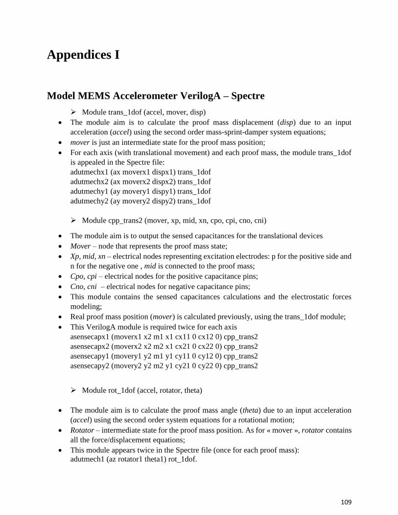
109
Appendices I
Model MEMS Accelerometer VerilogA – Spectre
Module trans_1dof (accel, mover, disp)
• The module aim is to calculate the proof mass displacement (disp) due to an input
acceleration (accel) using the second order mass-sprint-damper system equations;
• mover is just an intermediate state for the proof mass position;
• For each axis (with translational movement) and each proof mass, the module trans_1dof
is appealed in the Spectre file:
adutmechx1 (ax moverx1 dispx1) trans_1dof
adutmechx2 (ax moverx2 dispx2) trans_1dof
adutmechy1 (ay movery1 dispy1) trans_1dof
adutmechy2 (ay movery2 dispy2) trans_1dof
Module cpp_trans2 (mover, xp, mid, xn, cpo, cpi, cno, cni)
• The module aim is to output the sensed capacitances for the translational devices
• Mover – node that represents the proof mass state;
• Xp, mid, xn – electrical nodes representing excitation electrodes: p for the positive side and
n for the negative one , mid is connected to the proof mass;
• Cpo, cpi – electrical nodes for the positive capacitance pins;
• Cno, cni – electrical nodes for negative capacitance pins;
• This module contains the sensed capacitances calculations and the electrostatic forces
modeling;
• Real proof mass position (mover) is calculated previously, using the trans_1dof module;
• This VerilogA module is required twice for each axis
asensecapx1 (moverx1 x2 m1 x1 cx11 0 cx12 0) cpp_trans2
asensecapx2 (moverx2 x2 m2 x1 cx21 0 cx22 0) cpp_trans2
asensecapy1 (movery1 y2 m1 y1 cy11 0 cy12 0) cpp_trans2
asensecapy2 (movery2 y2 m2 y1 cy21 0 cy22 0) cpp_trans2
Module rot_1dof (accel, rotator, theta)
• The module aim is to calculate the proof mass angle (theta) due to an input acceleration
(accel) using the second order system equations for a rotational motion;
• Rotator – intermediate state for the proof mass position. As for « mover », rotator contains
all the force/displacement equations;
• This module appears twice in the Spectre file (once for each proof mass):
adutmech1 (az rotator1 theta1) rot_1dof.
APPENDICES I
110
adutmech2 (az rotator2 theta2) rot_1dof
Module cpp_rot_bigap (rotator, vp, vmid, vn, cpo, cpi, cno, cni)
• This module describes a differential bigap rotating parallel plate capacitor;
• Rotator is the proof mass position calculated using the module rot_1dof ;
• Vp, vn are the model excitation electrodes and vmid is the proof mass node;
• Cpo, cpi – electrical nodes for the positive capacitance pins;
• Cno, cni – electrical nodes for the negative capacitance pins;
• Simpson’s rule of integration is used to calculate capacitances and electrostatic forces:
• ∫ 𝑓(𝑥) ≈𝑏−𝑎
6[𝑓(𝑎) + 4𝑓 (
𝑎+𝑏
2) + 𝑓(𝑏)]
𝑏
𝑎
• This is being implemented for convergence/stable solutions
• The module is used in the Spectre file (once for each proof mass):
asensecap1 (rotator1 z2 m1 z1 cz11 0 cz12 0) cpp_rot_bigap
asensecap2 (rotator2 z2 m2 z1 cz 21 0 cz22 0) cpp_rot_bigap
A. model_heka.scs
simulator lang=spectre
library heka_model
//***********************************************************
section base
//***********************************************************
modelOptions options scale=1u gmin=1e-12 tnom=(27)
parameters
+ sDOTpercent = (0)
+ sDOTmult = (1)
+ sDOTmult2 = (1)
+ pi4models = (3.141592654)
+ nil = (0)
real mod(real a, real b)
return a-b*int((a+0.5)/b); // a and b must be positive
real sgn(real a)
return ((a>0)-(a<0));
real shrnk(real udr, real sDOTmult)
return (udr*sDOTmult) ;
APPENDICES I
111
adutmech2 (az rotator2 theta2) rot_1dof
Module cpp_rot_bigap (rotator, vp, vmid, vn, cpo, cpi, cno, cni)
• This module describes a differential bigap rotating parallel plate capacitor;
• Rotator is the proof mass position calculated using the module rot_1dof ;
• Vp, vn are the model excitation electrodes and vmid is the proof mass node;
• Cpo, cpi – electrical nodes for the positive capacitance pins;
• Cno, cni – electrical nodes for the negative capacitance pins;
• Simpson’s rule of integration is used to calculate capacitances and electrostatic forces:
• ∫ 𝑓(𝑥) ≈𝑏−𝑎
6[𝑓(𝑎) + 4𝑓 (
𝑎+𝑏
2) + 𝑓(𝑏)]
𝑏
𝑎
• This is being implemented for convergence/stable solutions
• The module is used in the Spectre file (once for each proof mass):
asensecap1 (rotator1 z2 m1 z1 cz11 0 cz12 0) cpp_rot_bigap
asensecap2 (rotator2 z2 m2 z1 cz 21 0 cz22 0) cpp_rot_bigap
B. model_heka.scs
simulator lang=spectre
library heka_model
//***********************************************************
section base
//***********************************************************
modelOptions options scale=1u gmin=1e-12 tnom=(27)
parameters
+ sDOTpercent = (0)
+ sDOTmult = (1)
+ sDOTmult2 = (1)
+ pi4models = (3.141592654)
+ nil = (0)
real mod(real a, real b)
return a-b*int((a+0.5)/b); // a and b must be positive
real sgn(real a)
return ((a>0)-(a<0));
real shrnk(real udr, real sDOTmult)
return (udr*sDOTmult) ;
APPENDICES I
112
real pwr(real x, real y)
return (x**y) ;
//***********************************************************
endsection base
//***********************************************************
//***********************************************************
section hdpoly_process_params
//***********************************************************
parameters
+ nom_tt = (25)
+ nom_cd = (-0.2)
+ nom_psg1 = (0.9)
+ nom_psg2 = (1.8)
+ nom_dela_cd = (0)
+ nom_delr_tt = (1.0)
+ nom_delr_psg1 = (1.0)
+ nom_delr_psg2 = (1.0)
+ nom_dela_x1o = (0.0)
+ nom_dela_x2o = (0.0)
+ nom_dela_y1o = (0.0)
+ nom_dela_y2o = (0.0)
+ nom_dela_z1o = (0.0)
+ nom_dela_z2o = (0.0)
+ sig_dela_cd = (0.045)
+ sig_delr_tt = (0.033)
+ sig_delr_psg1 = (0.033)
+ sig_delr_psg2 = (0.033)
+ sig_dela_x1o = (0.01)
+ sig_dela_x2o = (0.01)
+ sig_dela_y1o = (0.01)
+ sig_dela_y2o = (0.01)
+ sig_dela_z1o = (1e-6)
+ sig_dela_z2o = (1e-6)
//***********************************************************
endsection hdpoly_process_params
//***********************************************************
//***********************************************************
section typ_mems_process_params
//***********************************************************
APPENDICES I
113
parameters
+ nsig_dela_cd = (0)
+ nsig_dela_x1o = (0)
+ nsig_dela_x2o = (0)
+ nsig_dela_y1o = (0)
+ nsig_dela_y2o = (0)
+ nsig_dela_z1o = (0)
+ nsig_dela_z2o = (0)
+ nsig_delr_tt = (0)
+ nsig_delr_psg1 = (0)
+ nsig_delr_psg2 = (0)
//***********************************************************
endsection typ_mems_process_params
//***********************************************************
//***********************************************************
section mems
//***********************************************************
ahdl_include "$WORKAREA_DIR/veyron_sim/models/genericmems_heka.va"
parameters
+ dela_cd = (nom_dela_cd+nsig_dela_cd*sig_dela_cd)
+ dela_z1o = (nom_dela_z1o+nsig_dela_z1o*sig_dela_z1o)
+ delr_tt = (nom_delr_tt*(1+nsig_delr_tt*sig_delr_tt))
+ delr_psg1 =(nom_delr_psg1*(1+nsig_delr_psg1*sig_delr_psg1))
+ delr_psg2 =(nom_delr_psg2*(1+nsig_delr_psg2*sig_delr_psg2))
+ cdval = nom_cd+dela_cd
+ ttval = (nom_tt*delr_tt)
+ psg1val = (nom_psg1*delr_psg1)
+ psg2val = (nom_psg2*delr_psg2)
subckt heka (ax ay az z1 y1 x1 m1 m2 x2 y2 z2 sub cx11 cx12 cx21 cx22
cy11 cy12 cy21 cy22 cz11 cz12 cz21 cz22 cst1b cst2a dispx1 dispx2
dispy1 dispy2 theta1 theta2)
parameters
+ wfactor = ((2.0+cdval)^3)/((2.0+nom_cd)^3)
adutmechy1 (ay movery1 dispy1) trans_1dof
+ ks=(3.5*delr_tt*wfactor)
+ mass=(5.52e-9)
+ damp_ratio=(0.53)
+ orient=(1.0)
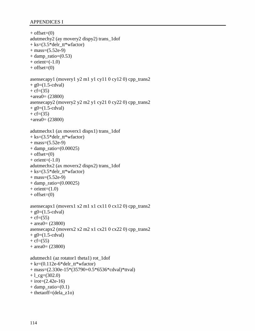
APPENDICES I
114
+ offset=(0)
adutmechy2 (ay movery2 dispy2) trans_1dof
+ ks=(3.5*delr_tt*wfactor)
+ mass=(5.52e-9)
+ damp_ratio=(0.53)
+ orient=(-1.0)
+ offset=(0)
asensecapy1 (movery1 y2 m1 y1 cy11 0 cy12 0) cpp_trans2
+ g0=(1.5-cdval)
+ cf=(35)
+area0= (23800)
asensecapy2 (movery2 y2 m2 y1 cy21 0 cy22 0) cpp_trans2
+ g0=(1.5-cdval)
+ cf=(35)
+area0= (23800)
adutmechx1 (ax moverx1 dispx1) trans_1dof
+ ks=(3.5*delr_tt*wfactor)
+ mass=(5.52e-9)
+ damp_ratio=(0.00025)
+ offset=(0)
+ orient=(-1.0)
adutmechx2 (ax moverx2 dispx2) trans_1dof
+ ks=(3.5*delr_tt*wfactor)
+ mass=(5.52e-9)
+ damp_ratio=(0.00025)
+ orient=(1.0)
+ offset=(0)
asensecapx1 (moverx1 x2 m1 x1 cx11 0 cx12 0) cpp_trans2
+ g0=(1.5-cdval)
+ cf=(55)
+ area0= (23800)
asensecapx2 (moverx2 x2 m2 x1 cx21 0 cx22 0) cpp_trans2
+ g0=(1.5-cdval)
+ cf=(55)
+ area0= (23800)
adutmech1 (az rotator1 theta1) rot_1dof
+ kr=(0.112e-6*delr_tt*wfactor)
+ mass=(2.330e-15*(35790+0.5*6536*cdval)*ttval)
+ l_cg=(302.0)
+ irot=(2.42e-16)
+ damp_ratio=(0.1)
+ thetaoff=(dela_z1o)

APPENDICES I
115
+ orient=(1.0)
adutmech2 (az rotator2 theta2) rot_1dof
+ kr=(0.112e-6*delr_tt*wfactor)
+ mass=(2.330e-15*(35790+0.5*6536*cdval)*ttval)
+ l_cg=(+302.0)
+ irot=(2.42e-16)
+ damp_ratio=(0.1)
+ thetaoff=(dela_z1o)
+ orient=(-1.0)
asensecap1 (rotator1 z2 m1 z1 cz11 0 cz12 0) cpp_rot_bigap
+ areafill_cap1=(0.84)
+ areafill_cap2=(0.875)
+ width0=(150.0)
+ l1=(60.0)
+ l2=(162.0)
+ l3=(233.0)
+ g1=(psg1val)
+ g2=(psg2val)
+ cf=(7)
asensecap2 (rotator2 z2 m2 z1 cz21 0 cz22 0) cpp_rot_bigap
+ areafill_cap1=(0.84)
+ areafill_cap2=(0.875)
+ width0=(150.0)
+ l1=(60.0)
+ l2=(162.0)
+ l3=(233.0)
+ g1=(psg1val)
+ g2=(psg2val)
+ cf=(7)
ends
//***********************************************************
endsection mems
//***********************************************************
endlibrary heka_model
C. genericmems_heka.va
`include "discipline.h"
`include "constants.h"
////////////////////////////////////////////////////////////////////////////////////////////////////////////////////////////////////////////
APPENDICES I
116
`define pi 3.14159265 // Ratio of circle circumference to diameter
`define eps0um 8.854e-18 // Permittivity of air / vacuum [F/um]
`define eps0m 8.854e-12 // Permittivity of air / vacuum [F/m]
`define k_boltz 1.38065e-23 // Boltzmann's constant [J/K]
`ifdef insideADMS
`ifdef notInsideADMS
`undef notInsideADMS
`endif
`else
`define notInsideADMS
`endif
`ifdef __VAMS_COMPACT_MODELING__
`ifdef not__VAMS_COMPACT_MODELING__
`undef not__VAMS_COMPACT_MODELING__
`endif
`else
`define not__VAMS_COMPACT_MODELING__
`endif
`ifdef __VAMS_COMPACT_MODELING__
`ifdef insideADMS
`define IPRcc(nam,def,uni,lwr,upr,des) (*units=uni, type="instance", ask="yes",
desc=des*) parameter real nam=def from[lwr:upr];
`define IPRco(nam,def,uni,lwr,upr,des) (*units=uni,type="instance", ask="yes", desc=des*)
parameter real nam=def from[lwr:upr);
`define IPRoc(nam,def,uni,lwr,upr,des) (*units=uni, type="instance", ask="yes",
desc=des*) parameter real nam=def from(lwr:upr];
`define IPRoo(nam,def,uni,lwr,upr,des) (*units=uni,type="instance", ask="yes", desc=des*)
parameter real nam=def from(lwr:upr);
`define IPRnb(nam,def,uni, des) (*units=uni, type="instance", ask="yes", desc=des*)
parameter real nam=def;
`define IPIcc(nam,def,uni,lwr,upr,des) (*units=uni,type="instance", ask="yes", desc=des*)
parameter integer nam=def from[lwr:upr];
`define IPIco(nam,def,uni,lwr,upr,des) (*units=uni,type="instance", ask="yes", desc=des*)
parameter integer nam=def from[lwr:upr);
`define IPIoc(nam,def,uni,lwr,upr,des) (*units=uni,type="instance", ask="yes", desc=des*)
parameter integer nam=def from(lwr:upr];
`define IPIoo(nam,def,uni,lwr,upr,des) (*units=uni,type="instance", ask="yes", desc=des*)
parameter integer nam=def from(lwr:upr);
APPENDICES I
117
`define IPInb(nam,def,uni, des) (*units=uni,type="instance", ask="yes", desc=des*)
parameter integer nam=def;
`define IPIsw(nam,def,uni, des) (*units=uni,type="instance", ask="yes", desc=des*)
parameter integer nam=def from[ 0: 1];
`else // notInsideADMS
`define IPRcc(nam,def,uni,lwr,upr,des) (*units=uni,desc=des*) parameter real nam=def
from[lwr:upr];
`define IPRco(nam,def,uni,lwr,upr,des) (*units=uni,desc=des*) parameter real nam=def
from[lwr:upr);
`define IPRoc(nam,def,uni,lwr,upr,des) (*units=uni,desc=des*) parameter real nam=def
from(lwr:upr];
`define IPRoo(nam,def,uni,lwr,upr,des) (*units=uni,desc=des*) parameter real nam=def
from(lwr:upr);
`define IPRnb(nam,def,uni, des) (*units=uni,desc=des*) parameter real nam=def;
`define IPIcc(nam,def,uni,lwr,upr,des) (*units=uni,desc=des*) parameter integer nam=def
from[lwr:upr];
`define IPIco(nam,def,uni,lwr,upr,des) (*units=uni,desc=des*) parameter integer nam=def
from[lwr:upr);
`define IPIoc(nam,def,uni,lwr,upr,des) (*units=uni,desc=des*) parameter integer nam=def
from(lwr:upr];
`define IPIoo(nam,def,uni,lwr,upr,des) (*units=uni,desc=des*) parameter integer nam=def
from(lwr:upr);
`define IPInb(nam,def,uni, des) (*units=uni,desc=des*) parameter integer nam=def;
`define IPIsw(nam,def,uni, des) (*units=uni,desc=des*) parameter integer nam=def
from[ 0: 1];
`endif
`else // not__VAMS_COMPACT_MODELING__
`define IPRcc(nam,def,uni,lwr,upr,des) parameter real nam=def from[lwr:upr];
`define IPRco(nam,def,uni,lwr,upr,des) parameter real nam=def from[lwr:upr);
`define IPRoc(nam,def,uni,lwr,upr,des) parameter real nam=def from(lwr:upr];
`define IPRoo(nam,def,uni,lwr,upr,des) parameter real nam=def from(lwr:upr);
`define IPRnb(nam,def,uni, des) parameter real nam=def;
`define IPIcc(nam,def,uni,lwr,upr,des) parameter integer nam=def from[lwr:upr];
`define IPIco(nam,def,uni,lwr,upr,des) parameter integer nam=def from[lwr:upr);
`define IPIoc(nam,def,uni,lwr,upr,des) parameter integer nam=def from(lwr:upr];
`define IPIoo(nam,def,uni,lwr,upr,des) parameter integer nam=def from(lwr:upr);
`define IPInb(nam,def,uni, des) parameter integer nam=def;
`define IPIsw(nam,def,uni, des) parameter integer nam=def from[ 0: 1];
`endif
////////////////////////////////////////////////////////////////////////////////////////////////////////////////////////////////////////////
////////////////////////////////////////////////////////////////////////////////////////////////////////////////////////////////////////////
APPENDICES I
118
// Begin Module Definitions
////////////////////////////////////////////////////////////////////////////////////////////////////////////////////////////////////////////
// TRANSLATIONAL
////////////////////////////////////////////////////////////////////////////////////////////////////////////////////////////////////////////
// This model describes the translation motion of a 1-dof damped mechanical system
////////////////////////////////////////////////////////////////////////////////////////////////////////////////////////////////////////////
module trans_1dof (accel, mover, disp);
inout accel; // Applied acceleration - this is still an electrical state
inout mover; // Node that represents proof mass state in the x-direction
inout disp;
electrical accel; // Input acceleration in [m/s^2]
electrical mover; // [um]
electrical mov_vel; // [um/s]
electrical disp; // 1V = 1um
branch(mov_vel) vel_int; // Dummy node for mica topology checker
`IPRcc( damp_ratio , 1.5 ,"" , 0.0001, 5, "damping ratio")
`IPRoo( mass , 1e-9 ,"kg" ,1e-10, 1e-7, "mass of mover")
`IPRoo( ks , 5 ,"N/m" , 0.5, 100, "spring constant")
`IPRoo( tcs1 , 0 ,"N/m/K" , -1e-1, 1e-1, "tc1 of spring constant")
`IPRoo( tcs2 , 0 ,"N/m/K^2" , -1e-3, 1e-3, "tc2 of spring constant")
`IPRoo( tnom , 25.0 ,"C" , 0, 200, "nominal temperature")
`IPRcc( orient , 1.0 ,"C" ,-1.0, 1.0, "relative orientation")
`IPRoo( offset , 0 ,"um" ,-0.5, 0.5, "initial displacement")
`IPRoo( tco1 , 0 ,"N/m/K" , -1e-1, 1e-1, "tc1 of offset")
`IPRoo( tco2 , 0 ,"N/m/K^2" , -1e-3, 1e-3, "tc2 of offset")
real D_coef;
real ks_t, deltat,offset_t;
real Q_fact,natural_fo,rolloff_fo;
analog begin
`ifdef notInsideADMS
@(initial_step) begin
`endif
begin : initializeInstance
deltat = ($temperature-273.15-tnom);
APPENDICES I
119
ks_t = ks*(1+tcs1*deltat+tcs2*deltat*deltat);
offset_t = offset*(1+tco1*deltat+tco2*deltat*deltat);
D_coef = damp_ratio * 2* sqrt(ks*mass);
Q_fact = 1/(2*damp_ratio);
natural_fo = (sqrt(ks_t/mass) /(2*`pi)) * 1e-3;
rolloff_fo = sqrt( sqrt(pow(2*pow(damp_ratio,2)-1.0,2)+1) -(2*pow(damp_ratio,2)-1.0) )*
natural_fo;
//$strobe ("natural_fo\n", natural_fo);
//$strobe ("rolloff_fo\n", rolloff_fo);
end // initializeInstance
`ifdef notInsideADMS
end //intial step
`endif
begin : dynamicBlock
I(vel_int) <+ 1.0*V(mov_vel);
V(mov_vel) <+ ddt(V(mover));
I(mover) <+ orient*mass*V(accel)* 1.0e6 ; // Force of acceleration
I(mover) <+ -ks_t*V(mover); //Spring restoring force
I(mover) <+ -ks_t*offset_t; //Spring restoring force
I(mover) <+ -D_coef*V(mov_vel); // Damping
I(mover) <+ -mass*ddt(V(mov_vel), 1.0e-6); // Acceleration of mover substracts from
//total force
I(mover) <+white_noise(4.0e12*`k_boltz*$temperature*D_coef, "Brownian");
// Brownian noise
end // DynamicBlock
V(disp) <+ V(mover); // Monitor node for displacement
end // analog
endmodule //trans_1dof
////////////////////////////////////////////////////////////////////////////////////////////////////////////////////////////////////
////////////////////////////////////////////////////////////////////////////////////////////////////////////////////////////////////
// This module can be used for the sense and selftest capacitors on translational devices
// This approach uses linearization of electrostatic force to limit behavior instead of force
clamping
/////////////////////////////////////////////////////////////////////////////////////////////////////////////////
///////////////////////////////////////////////////////////////////////////////////////////////////////////////////////////////////////////
module cpp_trans2 (mover, xp, mid, xn, cpo,cpi, cno,cni);
inout mover; // Node that represents proof mass state
in the x-direction
APPENDICES I
120
inout xn,mid,xp;
inout cno, cpo;
inout cni, cpi;
electrical mover; // [um]
electrical xn,mid,xp;
electrical cno,cpo; // 1V = 1fF
electrical cni,cpi; // 1V = 1fF
voltage qn,qp;
voltage cnval,cpval;
`IPRcc( cf , 10 ,"" , 0.000000, 200, "parasitic capacitance")
`IPRoo( g0 , 1.5 ,"kg" ,0.2, 5, "initial gap")
`IPRoo( tco1 , 0 ,"um/K" ,-1e-1, 1e-1, "tc1 of offset")
`IPRoo( tco2 , 0 ,"um/K^2" ,-1e-3, 1e-3, "tc2 of offset")
`IPRoo( tnom , 25 ,"C" , 0, 200, "nominal temperature")
`IPRoo( nom_off , 0 ,"C" ,-2e-1, 2e-1, "nominal temperature")
`IPRoo( area0 , 0 ,"C" ,1e-9, 38000, "nominal temperature")
real mm_t, deltat;
real gap_p,gap_n;
real gap_p_tmp,gap_n_tmp;
real gap_p0,gap_n0;
real gap_min;
analog begin
`ifdef notInsideADMS
@(initial_step) begin
`endif
begin : initializeInstance
// area0 um^2
//$strobe("area0 \t= %g (kg) \n", area0);
begin : temperatureCoefficient
deltat = ($temperature-273.15-tnom);
mm_t = (nom_off+deltat*tco1+deltat*deltat*tco2);
end
gap_p0 = (g0 * (1-mm_t));
gap_n0 = (g0 * (1+mm_t));
gap_min = (0.01*g0);
APPENDICES I
121
end // initializeInstance
`ifdef notInsideADMS
end //intial step
`endif
begin : dynamicBlock
gap_p_tmp = gap_p0 + V(mover);
gap_n_tmp = gap_n0 - V(mover);
gap_p = gap_p_tmp;
gap_n = gap_n_tmp;
if (gap_p > gap_min) begin
I(mover) <+-0.5*`eps0um*1e12*area0*(V(xp,mid)*V(xp,mid)/(gap_p*gap_p));
V(cpval) <+ (`eps0um*area0*1e15/gap_p)+cf;
end else begin
I(mover) <+-0.5*`eps0um*1e12*area0*(V(xp,mid)*V(xp,mid)/(gap_min*gap_min));
V(cpval) <+((`eps0um*area0*1e15/gap_min)*(2-gap_p/gap_min))+cf;
end
if (gap_n > gap_min) begin
I(mover) <+0.5*`eps0um*1e12*area0*(V(xn,mid)*V(xn,mid)/(gap_n*gap_n));
V(cnval) <+ (`eps0um*area0*1e15/gap_n)+cf;
end else begin
I(mover) <+0.5*`eps0um*1e12*area0*(V(xn,mid)*V(xn,mid)/(gap_min*gap_min));
V(cnval) <+((`eps0um*area0*1e15/gap_min)*(2-gap_n/gap_min))+cf;
end
V(qn) <+ V(xn,mid)*V(cnval);
V(qp) <+ V(xp,mid)*V(cpval);
end // DynamicBlock
V(cno,cni) <+ V(cnval);
V(cpo,cpi) <+ V(cpval);
I(xn,mid) <+ ddt(V(qn))*1e-15;
I(xp,mid) <+ ddt(V(qp))*1e-15;
end // analog
endmodule //cpp_trans2
APPENDICES I
122
//////////////////////////////////////////////////////////////////////////////////////////////////////////////////////
/// This is a one-sided capacitor module for single ended self-test modules
//////////////////////////////////////////////////////////////////////////////////////////////////////////////////////
module cpp_trans_1side (mover, xst, mid, csto,csti);
inout mover; // Node that represents proof mass state
in the x-direction
inout xst,mid;
inout csto, csti;
electrical mover; // [um]
electrical xst,mid;
electrical csto,csti; // 1V = 1fF
voltage qst;
voltage cstval;
`IPRcc( tt , 25 ,"" , 0.05, 5000, "nominal capacitance")
`IPRcc( tf , 0.85 ,"" , 0.05, 5000, "nominal capacitance")
`IPRcc( lf , 10 ,"" , 0.05, 5000, "nominal capacitance")
`IPRcc( nf , 1 ,"" , 1.00, 5000, "nominal capacitance")
`IPRcc( cf , 10 ,"" , 0.000000, 200, "parasitic capacitance")
`IPRoo( g0 , 1.5 ,"kg" ,0.2, 5, "initial gap")
`IPRoo( orient , 1 ,"C" ,-2, 2, "nominal temperature")
`IPRoo( tnom , 25 ,"C" ,0, 200, "nominal temperature")
real area0;
real mm_t, deltat;
real gap_st;
real gap_st_tmp;
real gap_st0;
real gap_min;
analog begin
`ifdef notInsideADMS
@(initial_step) begin
`endif
begin : initializeInstance
area0 = (tt+2*tf)*lf*nf; // um^2
begin : temperatureCoefficient
deltat = ($temperature-273.15-tnom);
end
APPENDICES I
123
gap_st0 = g0 ;
gap_min = (0.1*g0);
end // initializeInstance
`ifdef notInsideADMS
end //intial step
`endif
begin : dynamicBlock
gap_st_tmp = gap_st0 - V(mover)*orient;
gap_st = gap_st_tmp;
if (gap_st > gap_min) begin
I(mover) <+0.5*`eps0um*1e12*area0*orient*(V(xst,mid)*V(xst,mid)/(gap_st*gap_st));
V(cstval) <+ (`eps0um*area0*1e15/gap_st)+cf;
end else begin
I(mover)<+0.5*`eps0um*1e12*area0*orient*(V(xst,mid)*V(xst,mid)/(gap_min*gap_min));
V(cstval) <+((`eps0um*area0*1e15/gap_min)*(2-gap_st/gap_min))+cf;
end
V(qst) <+ V(xst,mid)*V(cstval);
V(csto,csti) <+ V(cstval);
I(xst,mid) <+ ddt(V(qst))*1e-15;
end // DynamicBlock
end // analog
endmodule //cpp_trans_1side
////////////////////////////////////////////////////////////////////////////////////////////////////////////////////////////////////////////
module stop_trans (mover);
inout mover; // Node that represents proof mass state
electrical mover;
electrical mov_vel;
`IPRoo( gap_stop , 0.70 ,"um" ,0.000001, inf, "Gap between stopper
and proof mass")
`IPRoo( ks_stop , 100 ,"N/m" , 0, inf, "Stiffness of mechanical stop")
`IPRoo( dmp_stop , 0.8 ,"N/m" , 0,inf, "Stiffness of mechanical stop")
parameter real eps = 1e-6;
real delta_p, delta_n;
APPENDICES I
124
real mod_delta_p, mod_delta_n;
analog begin
`ifdef notInsideADMS
@(initial_step) begin
`endif
begin : initializeInstance
end// initializeInstance
`ifdef notInsideADMS
end //intial step
`endif
begin : dynamicBlock
V(mov_vel) <+ ddt(V(mover));
delta_n = (V(mover)-gap_stop);
delta_p = (V(mover)+gap_stop);
mod_delta_n = 0.5*(delta_n+sqrt((delta_n)*(delta_n)+eps*eps));
mod_delta_p = 0.5*(delta_p-sqrt((delta_p)*(delta_p)+eps*eps));
I(mover) <+-ks_stop*(mod_delta_n+mod_delta_p)-ddt(mod_delta_n+mod_delta_p)*dmp_stop;
end // dynamicBlock
end // analog
endmodule
////////////////////////////////////////////////////////////////////////////////////////////////////////////////////////////////////////////
// ROTATIONAL
////////////////////////////////////////////////////////////////////////////////////////////////////////////////////////////////////////////
// This model describes a differential bigap rotating parallel plate capacitor
////////////////////////////////////////////////////////////////////////////////////////////////////////////////////////////////////////////
module cpp_rot_bigap (rotator, vp, vmid, vn, cpo,cpi, cno,cni);
inout rotator; // Node that represents proof mass rotation
about pivot point
inout vn,vmid,vp; // Electrodes
inout cno, cpo; // Monitoring nodes for capacitance
inout cni, cpi; // Monitoring nodes for capacitance
// Monitoring nodes are set up to be "stackable"
for parallel capacitances
APPENDICES I
125
electrical rotator; // [rad]
electrical vn,vmid,vp;
electrical cpo,cno; // 1V = 1fF
electrical cpi,cni; // 1V = 1fF
voltage qp,qn;
voltage cpvalv,cnvalv;
//branch (rotator) rot_int;
////////////////////////////////////////////////////////////////////////////////////////////////////////////////
// Model parameters
////////////////////////////////////////////////////////////////////////////////////////////////////////////////
`IPRcc( width0 , 200 ,"" , 0.05, 50000, "drawn area um^2")
`IPRcc( areafill_cap1 , 1 ,"" ,0.05, 1, "fill factor for capacitance")
`IPRcc( areafill_cap2 , areafill_cap1 ,"" , 0.05, 1, "fill factor for electrostatic force")
`IPRcc( l1 , 200 ,"" ,0.05, 5000, "inner distance from pivot to center of electrode ")
`IPRcc( l2 , 300 ,"" , 0.05, 5000, "bigap distance from pivot to center of electrode ")
`IPRcc( l3 , 400 ,"" , 0.05, 5000, "outer distance from pivot to center of electrode")
`IPRcc( cf , 10 ,"" , 0.00, 200, "parasitic capacitance")
`IPRoo( g1 , 0.9 ,"kg" , 0.2, 5, "initial inner gap")
`IPRoo( g2 , 1.8 ,"kg" , 0.2, 5, "initial outer gap")
`IPRoo( tc1 , 0 ,"rad/K" ,-1e-1, 1e-1, "tc1 of gap mismatch")
`IPRoo( tc2 , 0 ,"rad/K^2" ,-1e-3, 1e-3, "tc2 of gap mismatch")
`IPRoo( nom_g0_mm , 0 ,"C" ,-2e-1, 2e-1, "nominal offset Positive Cp >Cn ")
`IPRoo( tnom , 25 ,"C" , 0, 200, "nominal temperature")
real mm_t, deltat;
real gap_p1_tmp1,gap_n1_tmp1;
real gap_p1_tmpm,gap_n1_tmpm;
real gap_p1_tmp2,gap_n1_tmp2;
real gap_p1_max1,gap_n1_max1;
real gap_p1_maxm,gap_n1_maxm;
real gap_p1_max2,gap_n1_max2;
real gap_p2_tmp1,gap_n2_tmp1;
real gap_p2_tmpm,gap_n2_tmpm;
real gap_p2_tmp2,gap_n2_tmp2;
real gap_p2_max1,gap_n2_max1;
real gap_p2_maxm,gap_n2_maxm;
real gap_p2_max2,gap_n2_max2;
real gap_p10,gap_n10;
real gap_p20,gap_n20;
real gap_min1,gap_min2;
real thetamax1,thetamax2,thetamax;
real lm1,lm2;
real cnval,cpval;
APPENDICES I
126
real taup,taun;
real cnval1,cpval1;
real taup1,taun1;
real cnval2,cpval2;
real taup2,taun2;
real vfacp,vfacn;
real cpval_int1, cnval_int1;
real cpval_max1, cnval_max1;
real cpval_int2, cnval_int2;
real cpval_max2, cnval_max2;
analog begin
`ifdef notInsideADMS
@(initial_step) begin
`endif
begin : initializeInstance
lm1 = (l1+l2)/2.0;
lm2 = (l2+l3)/2.0;
gap_min1 = (0.1*g1);
gap_min2 = (0.1*g2);
thetamax1 = (g1-gap_min1)/l2;
thetamax2 = (g2-gap_min2)/l3;
// Determine which is the limiting gap
if (thetamax2 < thetamax1) begin
thetamax = thetamax2;
end else begin
thetamax = thetamax1;
end
begin : temperatureCoefficient
deltat = ($temperature-273.15-tnom);
mm_t = (nom_g0_mm*(1+deltat*tc1+deltat*deltat*tc2));
end
gap_p10 = (g1 * (1-mm_t));
gap_n10 = (g1 * (1+mm_t));
gap_p20 = (g2 * (1-mm_t));
gap_n20 = (g2 * (1+mm_t));
// Calculate min gap at "integration" points for simpson's method
gap_p1_max1 = gap_p10 - thetamax*l1;
gap_p1_maxm = gap_p10 - thetamax*lm1;
gap_p1_max2 = gap_p10 - thetamax*l2;
gap_n1_max1 = gap_n10 - thetamax*l1;
APPENDICES I
127
gap_n1_maxm = gap_n10 - thetamax*lm1;
gap_n1_max2 = gap_n10 - thetamax*l2;
gap_p2_max1 = gap_p20 - thetamax*l2;
gap_p2_maxm = gap_p20 - thetamax*lm2;
gap_p2_max2 = gap_p20 - thetamax*l3;
gap_n2_max1 = gap_n20 - thetamax*l2;
gap_n2_maxm = gap_n20 - thetamax*lm2;
gap_n2_max2 = gap_n20 - thetamax*l3;
cpval_int1 = (11/(gap_p1_max1*gap_p1_max1)+4*lm1/(gap_p1_maxm*gap_p1_maxm) +
l2/(gap_p1_max2*gap_p1_max2));
cnval_int1 = (11/(gap_n1_max1*gap_n1_max1)+4*lm1/(gap_n1_maxm*gap_n1_maxm) +
l2/(gap_n1_max2*gap_n1_max2));
cpval_max1 =(`eps0um*width0*(l2-l1)*1e15/6)*areafill_cap1*(1/gap_p1_max1
+4/gap_p1_maxm + 1/gap_p1_max2);
cnval_max1 =(`eps0um*width0*(l2-l1)*1e15/6)*areafill_cap1*(1/gap_n1_max1
+4/gap_n1_maxm + 1/gap_n1_max2);
cpval_int2 = (12/(gap_p2_max1*gap_p2_max1)+4*lm2/(gap_p2_maxm*gap_p2_maxm) +
l3/(gap_p2_max2*gap_p2_max2));
cnval_int2 = (12/(gap_n2_max1*gap_n2_max1)+4*lm2/(gap_n2_maxm*gap_n2_maxm) +
l3/(gap_n2_max2*gap_n2_max2));
cpval_max2=(`eps0um*width0*(l3-l2)*1e15/6)*areafill_cap2*(1/gap_p2_max1
+4/gap_p2_maxm + 1/gap_p2_max2);
cnval_max2 =(`eps0um*width0*(l3-l2)*1e15/6)*areafill_cap2*(1/gap_n2_max1
+4/gap_n2_maxm + 1/gap_n2_max2);
end // initializeInstance
`ifdef notInsideADMS
end //intial step
`endif
begin : dynamicBlock
gap_p1_tmp1 = gap_p10 - V(rotator)*l1;
gap_p1_tmpm = gap_p10 - V(rotator)*lm1;
gap_p1_tmp2 = gap_p10 - V(rotator)*l2;
gap_n1_tmp1 = gap_n10 + V(rotator)*l1;
gap_n1_tmpm = gap_n10 + V(rotator)*lm1;
gap_n1_tmp2 = gap_n10 + V(rotator)*l2;
gap_p2_tmp1 = gap_p20 - V(rotator)*l2;
gap_p2_tmpm = gap_p20 - V(rotator)*lm2;
gap_p2_tmp2 = gap_p20 - V(rotator)*l3;
gap_n2_tmp1 = gap_n20 + V(rotator)*l2;
gap_n2_tmpm = gap_n20 + V(rotator)*lm2;
APPENDICES I
128
gap_n2_tmp2 = gap_n20 + V(rotator)*l3;
vfacp = 0.5*(V(vp,vmid)*V(vp,vmid));
vfacn = 0.5*(V(vn,vmid)*V(vn,vmid));
// Calculate theta value to begin linearization of capacitance
// Use Simpson's rule of integration to calculate capacitances and electrostatic forces
// This is being done to avoid "exact" solution which has 1/theta term
// Create a linearization of the capacitance and electrostatic force above a certain value of theta
// This is being implemented for convergence/stable solutions in a spice-like circuit simulator
if (V(rotator) > thetamax) begin
cpval1 =(`eps0um*width0*(l2-l1)*1e15/6)*areafill_cap1*cpval_int1*(V(rotator)-
thetamax)+cpval_max1 ;
cnval1 =(`eps0um*width0*(l2-l1)*1e15/6)*areafill_cap1*(1/gap_n1_tmp1
+4/gap_n1_tmpm + 1/gap_n1_tmp2) ;
taup1 =vfacp*(`eps0um*width0*(l2-
l1)/6)*areafill_cap1*(l1/(gap_p1_max1*gap_p1_max1)+4*lm1/(gap_p1_maxm*gap_p1_maxm)
+ l2/(gap_p1_max2*gap_p1_max2));
taun1 =vfacn*(`eps0um*width0*(l2-
l1)/6)*areafill_cap1*(l1/(gap_n1_tmp1*gap_n1_tmp1)+4*lm1/(gap_n1_tmpm*gap_n1_tmpm) +
l2/(gap_n1_tmp2*gap_n1_tmp2));
cpval2 =(`eps0um*width0*1e15*(l3-l2)/6)*areafill_cap2*cpval_int2*(V(rotator)-
thetamax)+cpval_max2 ;
cnval2 =(`eps0um*width0*1e15*(l3-l2)/6)*areafill_cap2*(1/gap_n2_tmp1
+4/gap_n2_tmpm + 1/gap_n2_tmp2) ;
taup2 =vfacp*(`eps0um*width0*(l3-l2)/6)*areafill_cap2* (l2/(gap_p2_max1*
gap_p2_max1)+4*lm2/(gap_p2_maxm*gap_p2_maxm) + l3/(gap_p2_max2*gap_p2_max2));
taun2 =vfacn*(`eps0um*width0*(l3- l2)/6)*areafill_cap2 *(l2/(gap_n2_tmp1*
gap_n2_tmp1)+4*lm2/(gap_n2_tmpm*gap_n2_tmpm) + l3/(gap_n2_tmp2*gap_n2_tmp2));
cpval = cpval1 + cpval2 +cf;
cnval = cnval1 + cnval2 +cf;
taup = taup1 + taup2;
taun = taun1 + taun2;
end else if (V(rotator) < -1*thetamax) begin
cpval1 =(`eps0um*width0*1e15*(l2-l1)/6)*areafill_cap1*(1/gap_p1_tmp1
+4/gap_p1_tmpm + 1/gap_p1_tmp2) ;
cnval1 =-1.0*(`eps0um*width0*1e15*(l2-l1)/6)*areafill_cap1* cnval_int1*
(V(rotator)+thetamax)+cnval_max1;
taup1 =vfacp*(`eps0um*width0*(l2-l1)/6)*areafill_cap1* (l1/(gap_p1_tmp1*
gap_p1_tmp1)+4*lm1/(gap_p1_tmpm*gap_p1_tmpm) + l2/(gap_p1_tmp2*gap_p1_tmp2));
taun1 =vfacn*(`eps0um*width0*(l2-l1)/6)* areafill_cap1* (l1/(gap_n1_max1*
gap_n1_max1)+4*lm1/(gap_n1_maxm*gap_n1_maxm) + l2/(gap_n1_max2*gap_n1_max2));
APPENDICES I
129
cpval2 = (`eps0um*width0*1e15*(l3-l2)/6)*areafill_cap2*(1/gap_p2_tmp1
+4/gap_p2_tmpm + 1/gap_p2_tmp2) ;
cnval2 = -1.0*(`eps0um*width0*1e15*(l3-l2)/6)*areafill_cap2* cnval_int2*
(V(rotator)+thetamax)+cnval_max2;
taup2 =vfacp*(`eps0um*width0*(l3-l2)/6)*areafill_cap2* (l2/(gap_p2_tmp1*
gap_p2_tmp1)+4*lm2/(gap_p2_tmpm*gap_p2_tmpm) + l3/(gap_p2_tmp2*gap_p2_tmp2));
taun2 = vfacn*(`eps0um*width0*(l3-l2)/6)*areafill_cap2* (l2/(gap_n2_max1*
gap_n2_max1)+4*lm2/(gap_n2_maxm*gap_n2_maxm) + l3/(gap_n2_max2*gap_n2_max2));
cpval = cpval1 + cpval2 +cf;
cnval = cnval1 + cnval2 +cf;
taup = taup1 + taup2;
taun = taun1 + taun2;
end else begin
cpval1 =(`eps0um*width0*1e15*(l2-l1)/6)*areafill_cap1*(1/gap_p1_tmp1
+4/gap_p1_tmpm + 1/gap_p1_tmp2);
cnval1 =(`eps0um*width0*1e15*(l2-l1)/6)*areafill_cap1*(1/gap_n1_tmp1
+4/gap_n1_tmpm + 1/gap_n1_tmp2);
taup1 = vfacp*(`eps0um*width0*(l2-l1)/6)*areafill_cap1* (l1/(gap_p1_tmp1*
gap_p1_tmp1)+4*lm1/(gap_p1_tmpm*gap_p1_tmpm) + l2/(gap_p1_tmp2*gap_p1_tmp2));
taun1 = vfacn*(`eps0um*width0*(l2-
l1)/6)*areafill_cap1*(l1/(gap_n1_tmp1*gap_n1_tmp1) +4*lm1/(gap_n1_tmpm*gap_n1_tmpm)
+ l2/(gap_n1_tmp2*gap_n1_tmp2));
cpval2 =(`eps0um*width0*1e15*(l3-l2)/6)*areafill_cap2*(1/gap_p2_tmp1
+4/gap_p2_tmpm + 1/gap_p2_tmp2);
cnval2 =(`eps0um*width0*1e15*(l3-l2)/6)*areafill_cap2*(1/gap_n2_tmp1
+4/gap_n2_tmpm + 1/gap_n2_tmp2);
taup2 =vfacp*(`eps0um*width0*(l3-l2)/6)*areafill_cap2* (l2/(gap_p2_tmp1*
gap_p2_tmp1)+4*lm2/(gap_p2_tmpm*gap_p2_tmpm) + l3/(gap_p2_tmp2* gap_p2_tmp2));
taun2 =vfacn*(`eps0um*width0*(l3-l2)/6)*areafill_cap2*(l2/(gap_n2_tmp1*
gap_n2_tmp1)+4*lm2/(gap_n2_tmpm*gap_n2_tmpm) + l3/(gap_n2_tmp2*gap_n2_tmp2));
cpval = cpval1 + cpval2 +cf;
cnval = cnval1 + cnval2 +cf;
taup = taup1 + taup2;
taun = taun1 + taun2;
end
end // DynamicBlock
V(cpvalv) <+ (cpval);
V(cnvalv) <+ (cnval);
APPENDICES I
130
V(qn) <+ V(vn,vmid)*V(cnvalv);
V(qp) <+ V(vp,vmid)*V(cpvalv);
// This configuration is used to allow capacitance modules to be stacked in parallel and
provide total capacitance calculations
V(cno,cni) <+ V(cnvalv);
V(cpo,cpi) <+ V(cpvalv);
I(rotator) <+ (taup-taun);
I(vn,vmid) <+ ddt(V(qn))*1e-15;
I(vp,vmid) <+ ddt(V(qp))*1e-15;
end // analog
endmodule //cpp_rot_bigap
////////////////////////////////////////////////////////////////////////////////////////////////////////////////////////////////////////////
// This model describes a differential single rotating parallel plate capacitor
////////////////////////////////////////////////////////////////////////////////////////////////////////////////////////////////////////////
module cpp_rot (rotator, vp, vmid, cpo,cpi);
inout rotator; // Node that represents proof mass rotation
about pivot point
inout vmid,vp; // Electrodes
inout cpo; // Monitoring nodes for capacitance
inout cpi; // Monitoring nodes for capacitance
// Monitoring nodes are set up to be "stackable"
for parallel capacitances
electrical rotator; // [rad]
electrical vmid,vp;
electrical cpo; // 1V = 1fF
electrical cpi; // 1V = 1fF
voltage qp;
voltage cpvalv;
//branch (rotator) rot_int;
////////////////////////////////////////////////////////////////////////////////////////////////////////////////
// Model parameters
////////////////////////////////////////////////////////////////////////////////////////////////////////////////
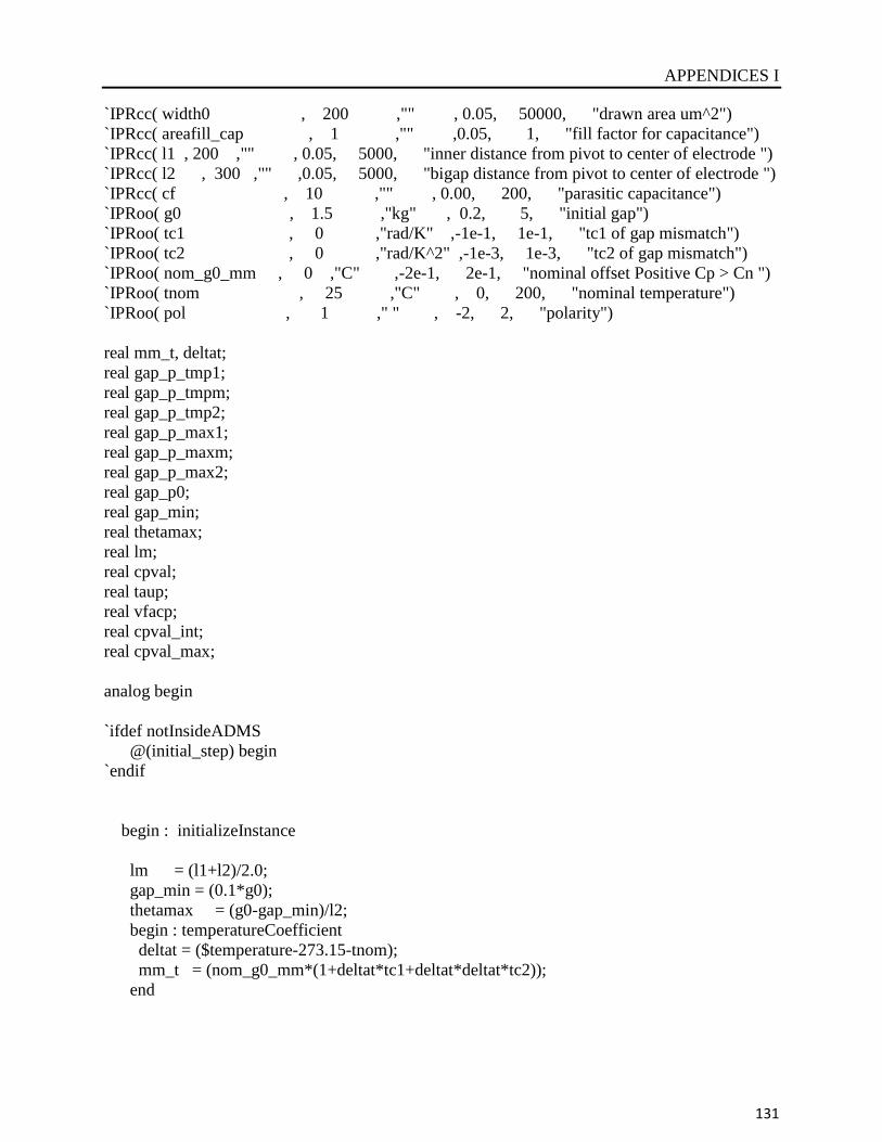
APPENDICES I
131
`IPRcc( width0 , 200 ,"" , 0.05, 50000, "drawn area um^2")
`IPRcc( areafill_cap , 1 ,"" ,0.05, 1, "fill factor for capacitance")
`IPRcc( l1 , 200 ,"" , 0.05, 5000, "inner distance from pivot to center of electrode ")
`IPRcc( l2 , 300 ,"" ,0.05, 5000, "bigap distance from pivot to center of electrode ")
`IPRcc( cf , 10 ,"" , 0.00, 200, "parasitic capacitance")
`IPRoo( g0 , 1.5 ,"kg" , 0.2, 5, "initial gap")
`IPRoo( tc1 , 0 ,"rad/K" ,-1e-1, 1e-1, "tc1 of gap mismatch")
`IPRoo( tc2 , 0 ,"rad/K^2" ,-1e-3, 1e-3, "tc2 of gap mismatch")
`IPRoo( nom_g0_mm , 0 ,"C" ,-2e-1, 2e-1, "nominal offset Positive Cp > Cn ")
`IPRoo( tnom , 25 ,"C" , 0, 200, "nominal temperature")
`IPRoo( pol , 1 ," " , -2, 2, "polarity")
real mm_t, deltat;
real gap_p_tmp1;
real gap_p_tmpm;
real gap_p_tmp2;
real gap_p_max1;
real gap_p_maxm;
real gap_p_max2;
real gap_p0;
real gap_min;
real thetamax;
real lm;
real cpval;
real taup;
real vfacp;
real cpval_int;
real cpval_max;
analog begin
`ifdef notInsideADMS
@(initial_step) begin
`endif
begin : initializeInstance
lm = (l1+l2)/2.0;
gap_min = (0.1*g0);
thetamax = (g0-gap_min)/l2;
begin : temperatureCoefficient
deltat = ($temperature-273.15-tnom);
mm_t = (nom_g0_mm*(1+deltat*tc1+deltat*deltat*tc2));
end
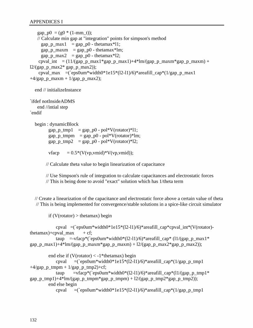
APPENDICES I
132
gap_p0 = (g0 * (1-mm_t));
// Calculate min gap at "integration" points for simpson's method
gap_p_max1 = gap_p0 - thetamax*l1;
gap_p_maxm = gap_p0 - thetamax*lm;
gap_p_max2 = gap_p0 - thetamax*l2;
cpval_int = (11/(gap_p_max1*gap_p_max1)+4*lm/(gap_p_maxm*gap_p_maxm) +
l2/(gap_p_max2* gap_p_max2));
cpval_max =(`eps0um*width0*1e15*(l2-l1)/6)*areafill_cap*(1/gap_p_max1
+4/gap_p_maxm + 1/gap_p_max2);
end // initializeInstance
`ifdef notInsideADMS
end //intial step
`endif
begin : dynamicBlock
gap_p_tmp1 = gap_p0 - pol*V(rotator)*l1;
gap_p_tmpm = gap_p0 - pol*V(rotator)*lm;
gap_p_tmp2 = gap_p0 - pol*V(rotator)*l2;
vfacp = 0.5*(V(vp,vmid)*V(vp,vmid));
// Calculate theta value to begin linearization of capacitance
// Use Simpson's rule of integration to calculate capacitances and electrostatic forces
// This is being done to avoid "exact" solution which has 1/theta term
// Create a linearization of the capacitance and electrostatic force above a certain value of theta
// This is being implemented for convergence/stable solutions in a spice-like circuit simulator
if (V(rotator) > thetamax) begin
cpval =(`eps0um*width0*1e15*(l2-l1)/6)*areafill_cap*cpval_int*(V(rotator)-
thetamax)+cpval_max + cf;
taup =-vfacp*(`eps0um*width0*(l2-l1)/6)*areafill_cap* (l1/(gap_p_max1*
gap_p_max1)+4*lm/(gap_p_maxm*gap_p_maxm) + l2/(gap_p_max2*gap_p_max2));
end else if (V(rotator) < -1*thetamax) begin
cpval =(`eps0um*width0*1e15*(l2-l1)/6)*areafill_cap*(1/gap_p_tmp1
+4/gap_p_tmpm + 1/gap_p_tmp2)+cf;
taup =vfacp*(`eps0um*width0*(l2-l1)/6)*areafill_cap*(l1/(gap_p_tmp1*
gap_p_tmp1)+4*lm/(gap_p_tmpm*gap_p_tmpm) + l2/(gap_p_tmp2*gap_p_tmp2));
end else begin
cpval =(`eps0um*width0*1e15*(l2-l1)/6)*areafill_cap*(1/gap_p_tmp1
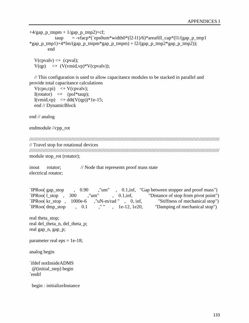
APPENDICES I
133
+4/gap_p_tmpm + 1/gap_p_tmp2)+cf;
taup = -vfacp*(`eps0um*width0*(l2-l1)/6)*areafill_cap*(l1/(gap_p_tmp1
*gap_p_tmp1)+4*lm/(gap_p_tmpm*gap_p_tmpm) + l2/(gap_p_tmp2*gap_p_tmp2));
end
V(cpvalv) <+ (cpval);
V(qp) <+ (V(vmid,vp)*V(cpvalv));
// This configuration is used to allow capacitance modules to be stacked in parallel and
provide total capacitance calculations
V(cpo,cpi) <+ V(cpvalv);
I(rotator) <+ (pol*taup);
I(vmid,vp) <+ ddt(V(qp))*1e-15;
end // DynamicBlock
end // analog
endmodule //cpp_rot
////////////////////////////////////////////////////////////////////////////////////////////////////////////////////////////////////////////
// Travel stop for rotational devices
////////////////////////////////////////////////////////////////////////////////////////////////////////////////////////////////////////////
module stop_rot (rotator);
inout rotator; // Node that represents proof mass state
electrical rotator;
`IPRoo( gap_stop , 0.90 ,"um" , 0.1,inf, "Gap between stopper and proof mass")
`IPRoo( l_stop , 300 ,"um" , 0.1,inf, "Distance of stop from pivot point")
`IPRoo( kr_stop , 1000e-6 ,"uN-m/rad " , 0, inf, "Stiffness of mechanical stop")
`IPRoo( dmp_stop , 0.1 ," " , 1e-12, 1e20, "Damping of mechanical stop")
real theta_stop;
real del_theta_n, del_theta_p;
real gap_n, gap_p;
parameter real eps = 1e-18;
analog begin
`ifdef notInsideADMS
@(initial_step) begin
`endif
begin : initializeInstance
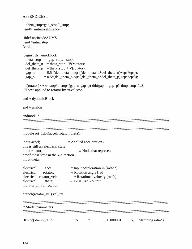
APPENDICES I
134
theta_stop=gap_stop/l_stop;
end// initializeInstance
`ifdef notInsideADMS
end //intial step
`endif
begin : dynamicBlock
theta_stop = gap_stop/l_stop;
del_theta_n = theta_stop - V(rotator);
del_theta_p = theta_stop + V(rotator);
gap_n = 0.5*(del_theta_n-sqrt((del_theta_n*del_theta_n)+eps*eps));
gap_p = 0.5*(del_theta_p-sqrt((del_theta_p*del_theta_p)+eps*eps));
I(rotator) <+kr_stop*l_stop*(gap_n-gap_p)-ddt(gap_n-gap_p)*dmp_stop*1e3;
//Force applied to rotator by travel stop
end // dynamicBlock
end // analog
endmodule
////////////////////////////////////////////////////////////////////////////////////////////////////////////////////////////////////////////
////////////////////////////////////////////////////////////////////////////////////////////////////////////////////////////////////////////
module rot_1dof(accel, rotator, theta);
inout accel; // Applied acceleration -
this is still an electrical state
inout rotator; // Node that represents
proof mass state in the x-direction
inout theta;
electrical accel; // Input acceleration in [m/s^2]
electrical rotator; // Rotation angle [rad]
electrical rotator_vel; // Rotational velocity [rad/s]
electrical theta; // 1V = 1rad - output
monitor pin for rotation
branch(rotator_vel) vel_int;
///////////////////////////////////////////////////////////////////////////////////////////////////////////////////////////////////////////
// Model parameters
////////////////////////////////////////////////////////////////////////////////////////////////////////////////////////////////////////////
`IPRcc( damp_ratio , 1.5 ,"" , 0.000001, 5, "damping ratio")
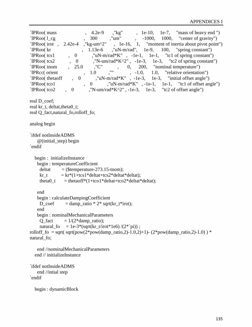
APPENDICES I
135
`IPRoo( mass , 4.2e-9 ,"kg" , 1e-10, 1e-7, "mass of heavy end ")
`IPRoo( l_cg , 300 ,"um" , -1000, 1000, "center of gravity")
`IPRoo( irot , 2.42e-4 ,"kg-um^2" , 1e-16, 1, "moment of inertia about pivot point")
`IPRoo( kr , 1.13e-6 ,"uN-m/rad", 1e-9, 100, "spring constant")
`IPRoo( tcs1 , 0 ,"uN-m/rad*K" , -1e-1, 1e-1, "tc1 of spring constant")
`IPRoo( tcs2 , 0 ,"N-um/rad*K^2" , -1e-3, 1e-3, "tc2 of spring constant")
`IPRoo( tnom , 25.0 ,"C" , 0, 200, "nominal temperature")
`IPRcc( orient , 1.0 ,"" , -1.0, 1.0, "relative orientation")
`IPRoo( thetaoff , 0 ,"uN-m/rad*K" , -1e-3, 1e-3, "initial offset angle")
`IPRoo( tco1 , 0 ,"uN-m/rad*K" , -1e-1, 1e-1, "tc1 of offset angle")
`IPRoo( tco2 , 0 ,"N-um/rad*K^2" , -1e-3, 1e-3, "tc2 of offset angle")
real D_coef;
real kr_t, deltat,theta0_t;
real Q_fact,natural_fo,rolloff_fo;
analog begin
`ifdef notInsideADMS
@(initial_step) begin
`endif
begin : initializeInstance
begin : temperatureCoefficient
deltat = ($temperature-273.15-tnom);
kr_t = kr*(1+tcs1*deltat+tcs2*deltat*deltat);
theta0_t = thetaoff*(1+tco1*deltat+tco2*deltat*deltat);
end
begin : calculateDampingCoefficient
D_coef = damp_ratio * 2* sqrt(kr_t*irot);
end
begin : nominalMechanicalParameters
Q_fact = 1/(2*damp_ratio);
natural_fo = 1e-3*(sqrt(kr_t/irot*1e6) /(2*`pi)) ;
rolloff_fo = sqrt( sqrt(pow(2*pow(damp_ratio,2)-1.0,2)+1)- (2*pow(damp_ratio,2)-1.0) ) *
natural_fo;
end //nominalMechanicalParameters
end // initializeInstance
`ifdef notInsideADMS
end //intial step
`endif
begin : dynamicBlock
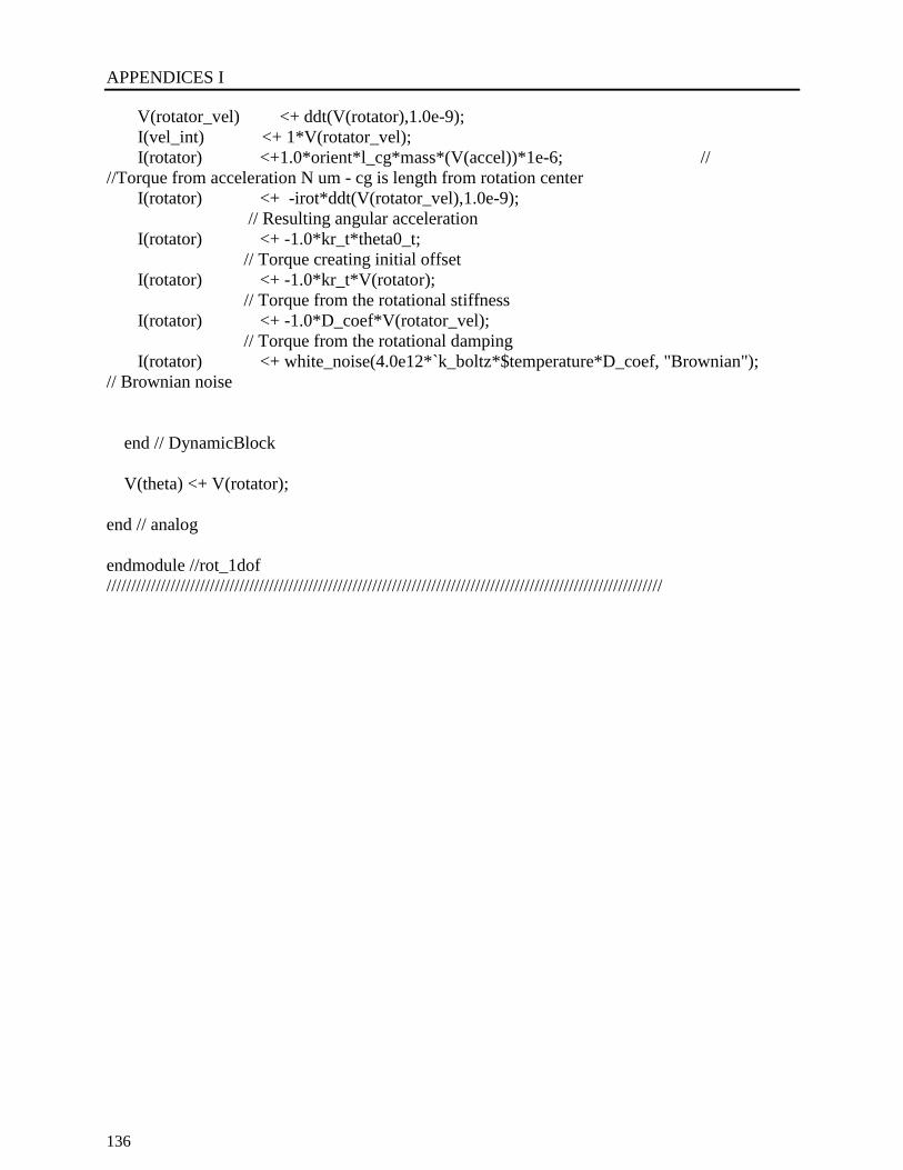
APPENDICES I
136
V(rotator_vel) <+ ddt(V(rotator),1.0e-9);
I(vel_int) <+ 1*V(rotator_vel);
I(rotator) <+1.0*orient*l_cg*mass*(V(accel))*1e-6; //
//Torque from acceleration N um - cg is length from rotation center
I(rotator) <+ -irot*ddt(V(rotator_vel),1.0e-9);
// Resulting angular acceleration
I(rotator) <+ -1.0*kr_t*theta0_t;
// Torque creating initial offset
I(rotator) <+ -1.0*kr_t*V(rotator);
// Torque from the rotational stiffness
I(rotator) <+ -1.0*D_coef*V(rotator_vel);
// Torque from the rotational damping
I(rotator) <+ white_noise(4.0e12*`k_boltz*$temperature*D_coef, "Brownian");
// Brownian noise
end // DynamicBlock
V(theta) <+ V(rotator);
end // analog
endmodule //rot_1dof
/////////////////////////////////////////////////////////////////////////////////////////////////////////////////
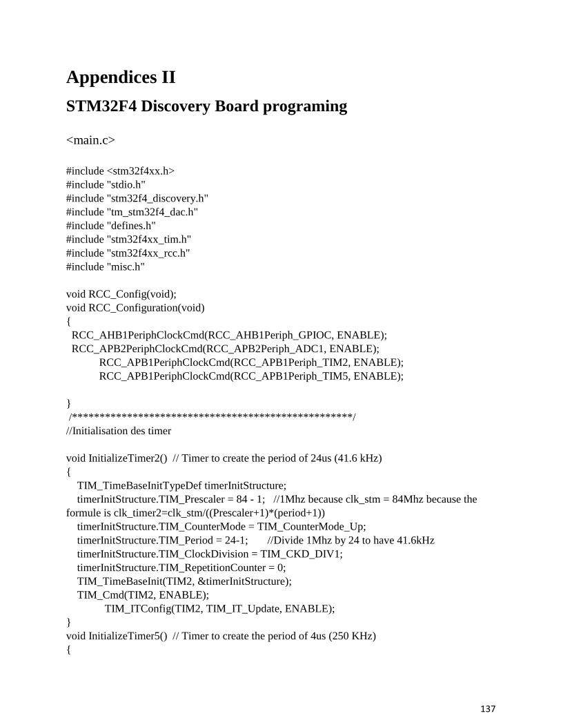
137
Appendices II
STM32F4 Discovery Board programing
<main.c>
#include <stm32f4xx.h>
#include "stdio.h"
#include "stm32f4_discovery.h"
#include "tm_stm32f4_dac.h"
#include "defines.h"
#include "stm32f4xx_tim.h"
#include "stm32f4xx_rcc.h"
#include "misc.h"
void RCC_Config(void);
void RCC_Configuration(void)
RCC_AHB1PeriphClockCmd(RCC_AHB1Periph_GPIOC, ENABLE);
RCC_APB2PeriphClockCmd(RCC_APB2Periph_ADC1, ENABLE);
RCC_APB1PeriphClockCmd(RCC_APB1Periph_TIM2, ENABLE);
RCC_APB1PeriphClockCmd(RCC_APB1Periph_TIM5, ENABLE);
/***************************************************/
//Initialisation des timer
void InitializeTimer2() // Timer to create the period of 24us (41.6 kHz)
TIM_TimeBaseInitTypeDef timerInitStructure;
timerInitStructure.TIM_Prescaler = 84 - 1; //1Mhz because clk_stm = 84Mhz because the
formule is clk_timer2=clk_stm/((Prescaler+1)*(period+1))
timerInitStructure.TIM_CounterMode = TIM_CounterMode_Up;
timerInitStructure.TIM_Period = 24-1; //Divide 1Mhz by 24 to have 41.6kHz
timerInitStructure.TIM_ClockDivision = TIM_CKD_DIV1;
timerInitStructure.TIM_RepetitionCounter = 0;
TIM_TimeBaseInit(TIM2, &timerInitStructure);
TIM_Cmd(TIM2, ENABLE);
TIM_ITConfig(TIM2, TIM_IT_Update, ENABLE);
void InitializeTimer5() // Timer to create the period of 4us (250 KHz)
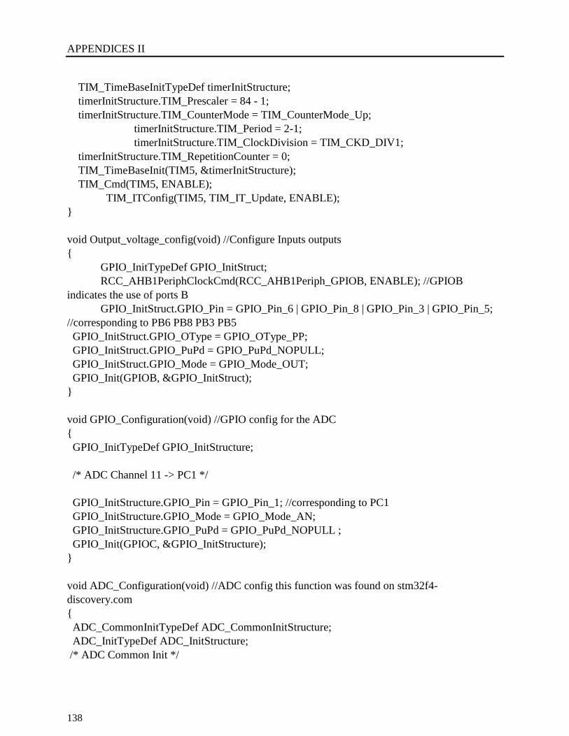
APPENDICES II
138
TIM_TimeBaseInitTypeDef timerInitStructure;
timerInitStructure.TIM_Prescaler = 84 - 1;
timerInitStructure.TIM_CounterMode = TIM_CounterMode_Up;
timerInitStructure.TIM_Period = 2-1;
timerInitStructure.TIM_ClockDivision = TIM_CKD_DIV1;
timerInitStructure.TIM_RepetitionCounter = 0;
TIM_TimeBaseInit(TIM5, &timerInitStructure);
TIM_Cmd(TIM5, ENABLE);
TIM_ITConfig(TIM5, TIM_IT_Update, ENABLE);
void Output_voltage_config(void) //Configure Inputs outputs
GPIO_InitTypeDef GPIO_InitStruct;
RCC_AHB1PeriphClockCmd(RCC_AHB1Periph_GPIOB, ENABLE); //GPIOB
indicates the use of ports B
GPIO_InitStruct.GPIO_Pin = GPIO_Pin_6 | GPIO_Pin_8 | GPIO_Pin_3 | GPIO_Pin_5;
//corresponding to PB6 PB8 PB3 PB5
GPIO_InitStruct.GPIO_OType = GPIO_OType_PP;
GPIO_InitStruct.GPIO_PuPd = GPIO_PuPd_NOPULL;
GPIO_InitStruct.GPIO_Mode = GPIO_Mode_OUT;
GPIO_Init(GPIOB, &GPIO_InitStruct);
void GPIO_Configuration(void) //GPIO config for the ADC
GPIO_InitTypeDef GPIO_InitStructure;
/* ADC Channel 11 -> PC1 */
GPIO_InitStructure.GPIO_Pin = GPIO_Pin_1; //corresponding to PC1
GPIO_InitStructure.GPIO_Mode = GPIO_Mode_AN;
GPIO_InitStructure.GPIO_PuPd = GPIO_PuPd_NOPULL ;
GPIO_Init(GPIOC, &GPIO_InitStructure);
void ADC_Configuration(void) //ADC config this function was found on stm32f4-
discovery.com
ADC_CommonInitTypeDef ADC_CommonInitStructure;
ADC_InitTypeDef ADC_InitStructure;
/* ADC Common Init */
APPENDICES II
139
ADC_CommonInitStructure.ADC_Mode = ADC_Mode_Independent;
ADC_CommonInitStructure.ADC_Prescaler = ADC_Prescaler_Div2;
ADC_CommonInitStructure.ADC_DMAAccessMode = ADC_DMAAccessMode_Disabled;
ADC_CommonInitStructure.ADC_TwoSamplingDelay = ADC_TwoSamplingDelay_5Cycles;
ADC_CommonInit(&ADC_CommonInitStructure);
ADC_InitStructure.ADC_Resolution = ADC_Resolution_12b;
ADC_InitStructure.ADC_ScanConvMode = DISABLE; // 1 Channel
ADC_InitStructure.ADC_ContinuousConvMode = DISABLE; // Conversions Triggered
ADC_InitStructure.ADC_ExternalTrigConvEdge = ADC_ExternalTrigConvEdge_None; //
Manual
ADC_InitStructure.ADC_ExternalTrigConv = ADC_ExternalTrigConv_T2_TRGO;
ADC_InitStructure.ADC_DataAlign = ADC_DataAlign_Right;
ADC_InitStructure.ADC_NbrOfConversion = 1;
ADC_Init(ADC1, &ADC_InitStructure);
/* ADC1 regular channel 11 configuration */
ADC_RegularChannelConfig(ADC1, ADC_Channel_11, 1, ADC_SampleTime_144Cycles); //
PC1
/* Enable ADC1 */
ADC_Cmd(ADC1, ENABLE);
/*****************************************************************************
*********/
uint16_t ADC_X1 = 0;
uint16_t calcul = 0;
uint16_t vitesse_X;
uint16_t ADCConvertedValue;
int main(void)
int j;
/* Initialize system */
RCC_Configuration();
GPIO_Configuration();
SystemInit();
/* Initialize DAC channel 2, pin PA5 */
TM_DAC_Init(TM_DAC2);
APPENDICES II
140
/* Initialize DAC channel 1, pin PA4 */
TM_DAC_Init(TM_DAC1); //PA4
//Init timer
InitializeTimer2();
InitializeTimer5();
//Init ADC
ADC_Configuration();
//Output init
Output_voltage_config(); //config output voltage
while (1) //infinite loop
ADC_SoftwareStartConv(ADC1); //this enables ADC
while(ADC_GetFlagStatus(ADC1, ADC_FLAG_EOC) == RESET);
if (TIM_GetITStatus(TIM2, TIM_IT_Update) != RESET)
//we manage the frequency 37kHz with the flag of timer2
for (j=1;j<13;j++)
while(TIM_GetITStatus(TIM5, TIM_IT_Update) == RESET);
//If the flag of the timer 660kHz doesn't change, we do nothing
TIM_ClearITPendingBit(TIM5, TIM_IT_Update);
//we clear the flag
switch(j)
case 1: //acquisition de la valeur de electrode_X
ADCConvertedValue = ADC_GetConversionValue(ADC1);
//We save the value of ADC
vitesse_X = ADCConvertedValue - ADC_X1;
//We calculate the "speed"
ADC_X1 = ADCConvertedValue;
//We save the value of ADC for the next passage in the loop
TM_DAC_SetValue(TM_DAC1, 0); //On envoie 0 pour X
//Outputs :
TM_DAC_SetValue(TM_DAC2, 0); //DAC2
TM_GPIO_SetPinLow(GPIOB,GPIO_Pin_6); //PWM3
TM_GPIO_SetPinLow(GPIOB,GPIO_Pin_8); //PWM4
TM_GPIO_SetPinHigh(GPIOB,GPIO_Pin_3); //PWM1
TM_GPIO_SetPinLow(GPIOB,GPIO_Pin_5); //PWM2
break;
case 2:
TM_DAC_SetValue(TM_DAC1, 0); //DAC1
APPENDICES II
141
TM_DAC_SetValue(TM_DAC2, 0); //DAC2
TM_GPIO_SetPinLow(GPIOB,GPIO_Pin_6); //PWM3
TM_GPIO_SetPinLow(GPIOB,GPIO_Pin_8); //PWM4
TM_GPIO_SetPinLow(GPIOB,GPIO_Pin_3); //PWM1
TM_GPIO_SetPinHigh(GPIOB,GPIO_Pin_5); //PWM2
break;
case 3:
calcul = 2048+vitesse_X; //VB=2048 (1.5V)
TM_DAC_SetValue(TM_DAC1, calcul);
TM_DAC_SetValue(TM_DAC2, 2048); //DAC2
TM_GPIO_SetPinHigh(GPIOB,GPIO_Pin_6); //PWM3
TM_GPIO_SetPinHigh(GPIOB,GPIO_Pin_8); //PWM4
TM_GPIO_SetPinLow(GPIOB,GPIO_Pin_3); //PWM1
TM_GPIO_SetPinLow(GPIOB,GPIO_Pin_5); //PWM2
break;
case 4 :
TM_DAC_SetValue(TM_DAC1,calcul);
TM_DAC_SetValue(TM_DAC2, 2048); //DAC2
TM_GPIO_SetPinHigh(GPIOB,GPIO_Pin_6); //PWM3
TM_GPIO_SetPinHigh(GPIOB,GPIO_Pin_8); //PWM4
TM_GPIO_SetPinLow(GPIOB,GPIO_Pin_3); //PWM1
TM_GPIO_SetPinLow(GPIOB,GPIO_Pin_5); //PWM2
break;
case 5 :
TM_DAC_SetValue(TM_DAC1, 0); //read y
TM_DAC_SetValue(TM_DAC2, 0); //DAC2
TM_GPIO_SetPinLow(GPIOB,GPIO_Pin_6); //PWM3
TM_GPIO_SetPinLow(GPIOB,GPIO_Pin_8); //PWM4
TM_GPIO_SetPinLow(GPIOB,GPIO_Pin_3); //PWM1
TM_GPIO_SetPinLow(GPIOB,GPIO_Pin_5); //PWM2
break;
case 6 :
TM_DAC_SetValue(TM_DAC1, 0); //read y
TM_DAC_SetValue(TM_DAC2, 0); //DAC2
TM_GPIO_SetPinLow(GPIOB,GPIO_Pin_6); //PWM3
TM_GPIO_SetPinLow(GPIOB,GPIO_Pin_8); //PWM4
TM_GPIO_SetPinLow(GPIOB,GPIO_Pin_3); //PWM1
TM_GPIO_SetPinLow(GPIOB,GPIO_Pin_5); //PWM2
break;
APPENDICES II
142
case 7 :
TM_DAC_SetValue(TM_DAC1, calcul);
TM_DAC_SetValue(TM_DAC2, 2048); //DAC2
TM_GPIO_SetPinHigh(GPIOB,GPIO_Pin_6); //PWM3
TM_GPIO_SetPinHigh(GPIOB,GPIO_Pin_8); //PWM4
TM_GPIO_SetPinLow(GPIOB,GPIO_Pin_3); //PWM1
TM_GPIO_SetPinLow(GPIOB,GPIO_Pin_5); //PWM2
break;
case 8 :
TM_DAC_SetValue(TM_DAC1, calcul);
TM_DAC_SetValue(TM_DAC2, 2048); //DAC2
TM_GPIO_SetPinHigh(GPIOB,GPIO_Pin_6); //PWM3
TM_GPIO_SetPinHigh(GPIOB,GPIO_Pin_8); //PWM4
TM_GPIO_SetPinLow(GPIOB,GPIO_Pin_3); //PWM1
TM_GPIO_SetPinLow(GPIOB,GPIO_Pin_5); //PWM2
break;
case 9 :
TM_DAC_SetValue(TM_DAC1, 0); //read z
TM_DAC_SetValue(TM_DAC2, 0); //DAC2
TM_GPIO_SetPinLow(GPIOB,GPIO_Pin_6); //PWM3
TM_GPIO_SetPinLow(GPIOB,GPIO_Pin_8); //PWM4
TM_GPIO_SetPinLow(GPIOB,GPIO_Pin_3); //PWM1
TM_GPIO_SetPinLow(GPIOB,GPIO_Pin_5); //PWM2
break;
case 10 :
TM_DAC_SetValue(TM_DAC1, 0); //read z
TM_DAC_SetValue(TM_DAC2, 0); //DAC2
TM_GPIO_SetPinLow(GPIOB,GPIO_Pin_6); //PWM3
TM_GPIO_SetPinLow(GPIOB,GPIO_Pin_8); //PWM4
TM_GPIO_SetPinLow(GPIOB,GPIO_Pin_3); //PWM1
TM_GPIO_SetPinLow(GPIOB,GPIO_Pin_5); //PWM2
break;
case 11:
TM_DAC_SetValue(TM_DAC1, calcul);
TM_DAC_SetValue(TM_DAC2, 2048); //DAC2
TM_GPIO_SetPinHigh(GPIOB,GPIO_Pin_6); //PWM3
TM_GPIO_SetPinHigh(GPIOB,GPIO_Pin_8); //PWM4
TM_GPIO_SetPinLow(GPIOB,GPIO_Pin_3); //PWM1
APPENDICES II
143
TM_GPIO_SetPinLow(GPIOB,GPIO_Pin_5); //PWM2
break;
case 12 :
TM_DAC_SetValue(TM_DAC1, calcul);
TM_DAC_SetValue(TM_DAC2, 2048); //DAC2
TM_GPIO_SetPinHigh(GPIOB,GPIO_Pin_6); //PWM3
TM_GPIO_SetPinHigh(GPIOB,GPIO_Pin_8); //PWM4
TM_GPIO_SetPinLow(GPIOB,GPIO_Pin_3); //PWM1
TM_GPIO_SetPinLow(GPIOB,GPIO_Pin_5); //PWM2
break;
default:
TM_GPIO_SetPinLow(GPIOB,GPIO_Pin_6); //PWM3
TM_GPIO_SetPinLow(GPIOB,GPIO_Pin_8); //PWM4
TM_GPIO_SetPinLow(GPIOB,GPIO_Pin_3); //PWM1
TM_GPIO_SetPinLow(GPIOB,GPIO_Pin_5); //PWM2
TIM_ClearITPendingBit(TIM2, TIM_IT_Update);
#ifdef USE_FULL_ASSERT
/**
* @brief Reports the name of the source file and the source line number
* where the assert_param error has occurred.
* @param file: pointer to the source file name
* @param line: assert_param error line source number
* @retval None
*/
void assert_failed(uint8_t* file, uint32_t line)
/* Infinite loop */
while (1)
#end

APPENDICES II
144
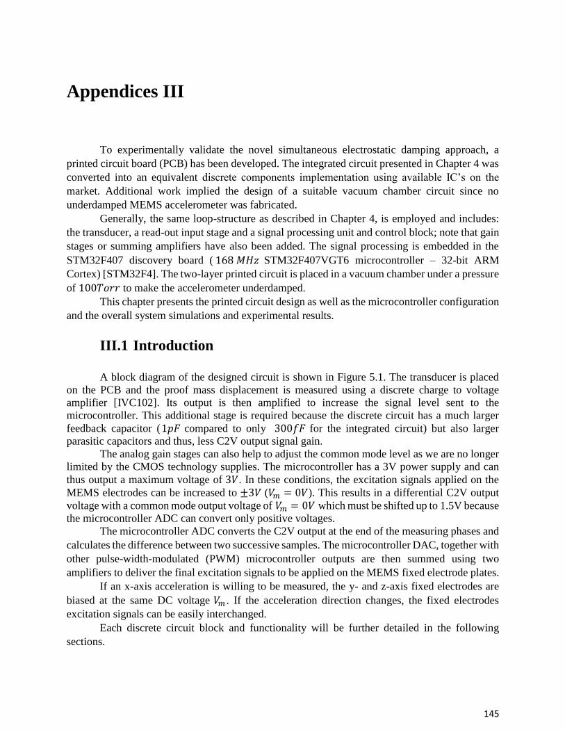
145
Appendices III
To experimentally validate the novel simultaneous electrostatic damping approach, a
printed circuit board (PCB) has been developed. The integrated circuit presented in Chapter 4 was
converted into an equivalent discrete components implementation using available IC’s on the
market. Additional work implied the design of a suitable vacuum chamber circuit since no
underdamped MEMS accelerometer was fabricated. Generally, the same loop-structure as described in Chapter 4, is employed and includes:
the transducer, a read-out input stage and a signal processing unit and control block; note that gain
stages or summing amplifiers have also been added. The signal processing is embedded in the
STM32F407 discovery board ( 168 𝑀𝐻𝑧 STM32F407VGT6 microcontroller – 32-bit ARM
Cortex) [STM32F4]. The two-layer printed circuit is placed in a vacuum chamber under a pressure
of 100𝑇𝑜𝑟𝑟 to make the accelerometer underdamped. This chapter presents the printed circuit design as well as the microcontroller configuration
and the overall system simulations and experimental results.
III.1 Introduction
A block diagram of the designed circuit is shown in Figure 5.1. The transducer is placed
on the PCB and the proof mass displacement is measured using a discrete charge to voltage
amplifier [IVC102]. Its output is then amplified to increase the signal level sent to the
microcontroller. This additional stage is required because the discrete circuit has a much larger
feedback capacitor (1𝑝𝐹 compared to only 300𝑓𝐹 for the integrated circuit) but also larger
parasitic capacitors and thus, less C2V output signal gain. The analog gain stages can also help to adjust the common mode level as we are no longer
limited by the CMOS technology supplies. The microcontroller has a 3V power supply and can
thus output a maximum voltage of 3𝑉. In these conditions, the excitation signals applied on the
MEMS electrodes can be increased to ±3𝑉 (𝑉𝑚 = 0𝑉). This results in a differential C2V output
voltage with a common mode output voltage of 𝑉𝑚 = 0𝑉 which must be shifted up to 1.5V because
the microcontroller ADC can convert only positive voltages. The microcontroller ADC converts the C2V output at the end of the measuring phases and
calculates the difference between two successive samples. The microcontroller DAC, together with
other pulse-width-modulated (PWM) microcontroller outputs are then summed using two
amplifiers to deliver the final excitation signals to be applied on the MEMS fixed electrode plates. If an x-axis acceleration is willing to be measured, the y- and z-axis fixed electrodes are
biased at the same DC voltage 𝑉𝑚 . If the acceleration direction changes, the fixed electrodes
excitation signals can be easily interchanged.
Each discrete circuit block and functionality will be further detailed in the following
sections.
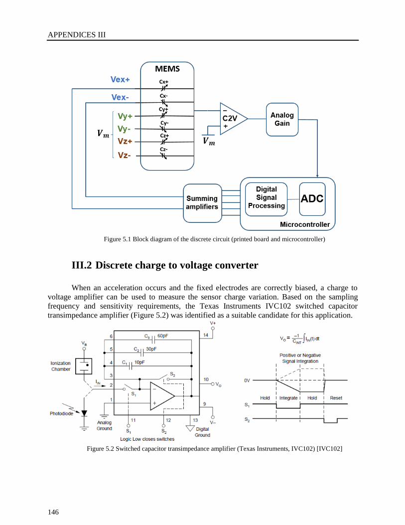
APPENDICES III
146
Figure 5.1 Block diagram of the discrete circuit (printed board and microcontroller)
III.2 Discrete charge to voltage converter
When an acceleration occurs and the fixed electrodes are correctly biased, a charge to
voltage amplifier can be used to measure the sensor charge variation. Based on the sampling
frequency and sensitivity requirements, the Texas Instruments IVC102 switched capacitor
transimpedance amplifier (Figure 5.2) was identified as a suitable candidate for this application.
Figure 5.2 Switched capacitor transimpedance amplifier (Texas Instruments, IVC102) [IVC102]
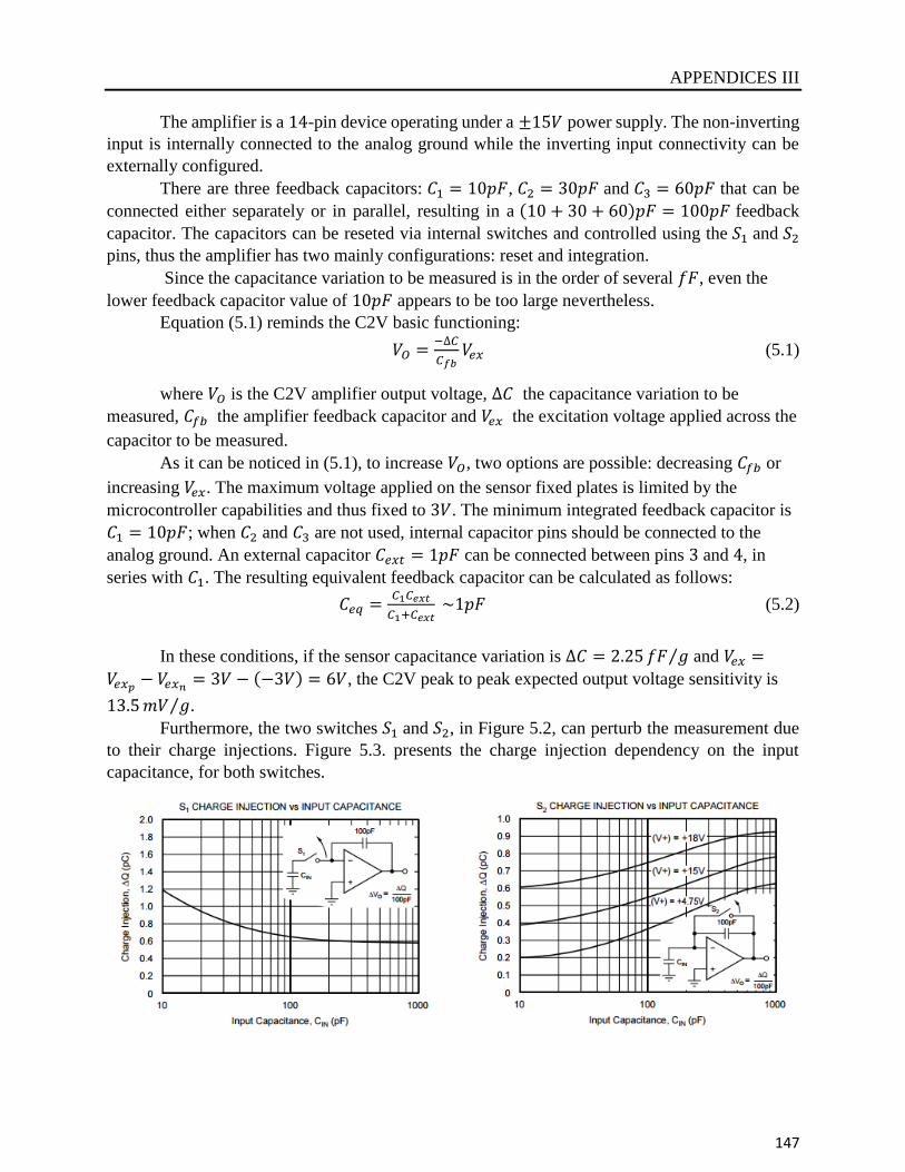
APPENDICES III
147
The amplifier is a 14-pin device operating under a ±15𝑉 power supply. The non-inverting
input is internally connected to the analog ground while the inverting input connectivity can be
externally configured.
There are three feedback capacitors: 𝐶1 = 10𝑝𝐹, 𝐶2 = 30𝑝𝐹 and 𝐶3 = 60𝑝𝐹 that can be
connected either separately or in parallel, resulting in a (10 + 30 + 60)𝑝𝐹 = 100𝑝𝐹 feedback
capacitor. The capacitors can be reseted via internal switches and controlled using the 𝑆1 and 𝑆2
pins, thus the amplifier has two mainly configurations: reset and integration.
Since the capacitance variation to be measured is in the order of several 𝑓𝐹, even the
lower feedback capacitor value of 10𝑝𝐹 appears to be too large nevertheless. Equation (5.1) reminds the C2V basic functioning:
𝑉𝑂 =−∆𝐶
𝐶𝑓𝑏𝑉𝑒𝑥 (5.1)
where 𝑉𝑂 is the C2V amplifier output voltage, ∆𝐶 the capacitance variation to be
measured, 𝐶𝑓𝑏 the amplifier feedback capacitor and 𝑉𝑒𝑥 the excitation voltage applied across the
capacitor to be measured.
As it can be noticed in (5.1), to increase 𝑉𝑂, two options are possible: decreasing 𝐶𝑓𝑏 or
increasing 𝑉𝑒𝑥. The maximum voltage applied on the sensor fixed plates is limited by the
microcontroller capabilities and thus fixed to 3𝑉. The minimum integrated feedback capacitor is
𝐶1 = 10𝑝𝐹; when 𝐶2 and 𝐶3 are not used, internal capacitor pins should be connected to the
analog ground. An external capacitor 𝐶𝑒𝑥𝑡 = 1𝑝𝐹 can be connected between pins 3 and 4, in
series with 𝐶1. The resulting equivalent feedback capacitor can be calculated as follows:
𝐶𝑒𝑞 =𝐶1𝐶𝑒𝑥𝑡
𝐶1+𝐶𝑒𝑥𝑡 ~1𝑝𝐹 (5.2)
In these conditions, if the sensor capacitance variation is ∆𝐶 = 2.25 𝑓𝐹 𝑔⁄ and 𝑉𝑒𝑥 =
𝑉𝑒𝑥𝑝− 𝑉𝑒𝑥𝑛
= 3𝑉 − (−3𝑉) = 6𝑉, the C2V peak to peak expected output voltage sensitivity is
13.5 𝑚𝑉 𝑔⁄ .
Furthermore, the two switches 𝑆1 and 𝑆2, in Figure 5.2, can perturb the measurement due
to their charge injections. Figure 5.3. presents the charge injection dependency on the input
capacitance, for both switches.
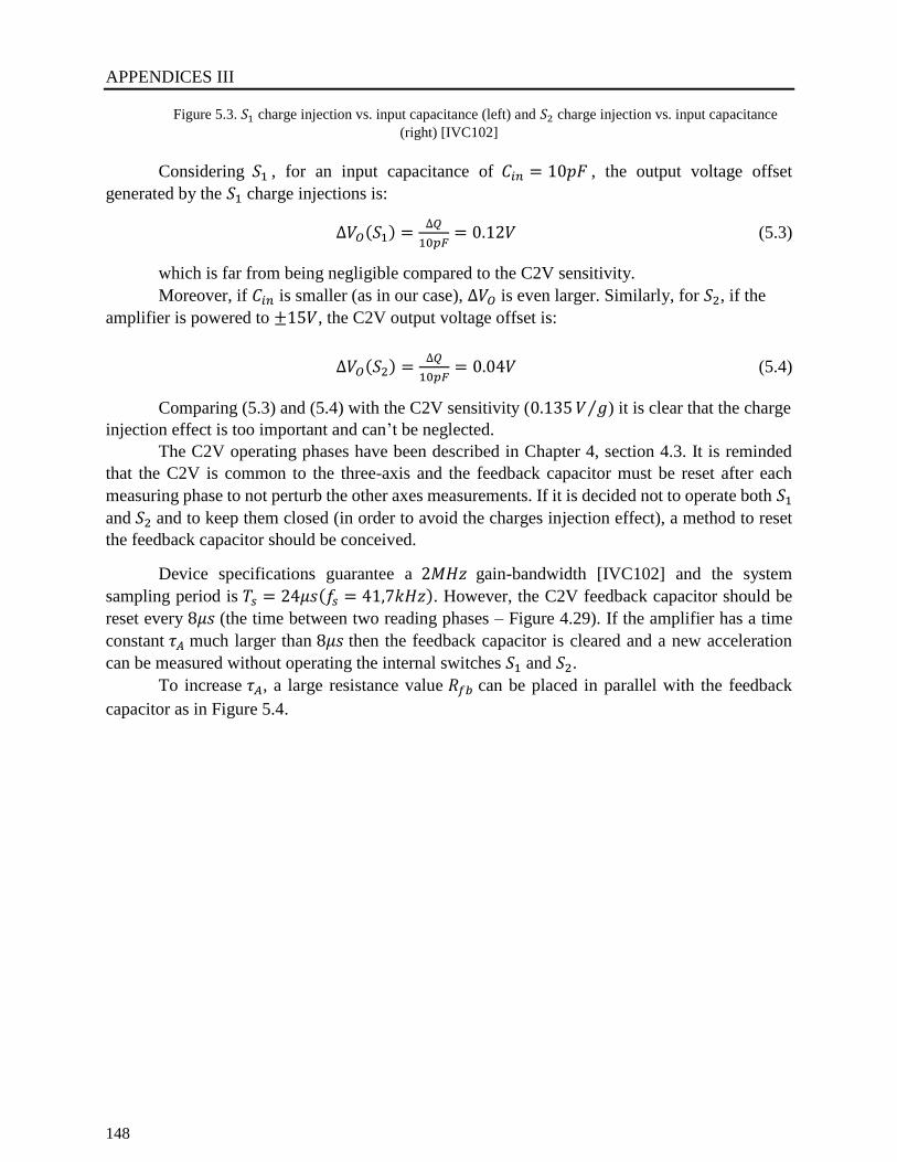
APPENDICES III
148
Figure 5.3. 𝑆1 charge injection vs. input capacitance (left) and 𝑆2 charge injection vs. input capacitance
(right) [IVC102]
Considering 𝑆1 , for an input capacitance of 𝐶𝑖𝑛 = 10𝑝𝐹 , the output voltage offset
generated by the 𝑆1 charge injections is:
∆𝑉𝑂(𝑆1) =∆𝑄
10𝑝𝐹= 0.12𝑉 (5.3)
which is far from being negligible compared to the C2V sensitivity.
Moreover, if 𝐶𝑖𝑛 is smaller (as in our case), ∆𝑉𝑂 is even larger. Similarly, for 𝑆2, if the
amplifier is powered to ±15𝑉, the C2V output voltage offset is:
∆𝑉𝑂(𝑆2) =∆𝑄
10𝑝𝐹= 0.04𝑉 (5.4)
Comparing (5.3) and (5.4) with the C2V sensitivity (0.135 𝑉 𝑔⁄ ) it is clear that the charge
injection effect is too important and can’t be neglected. The C2V operating phases have been described in Chapter 4, section 4.3. It is reminded
that the C2V is common to the three-axis and the feedback capacitor must be reset after each
measuring phase to not perturb the other axes measurements. If it is decided not to operate both 𝑆1
and 𝑆2 and to keep them closed (in order to avoid the charges injection effect), a method to reset
the feedback capacitor should be conceived.
Device specifications guarantee a 2𝑀𝐻𝑧 gain-bandwidth [IVC102] and the system
sampling period is 𝑇𝑠 = 24𝜇𝑠(𝑓𝑠 = 41,7𝑘𝐻𝑧). However, the C2V feedback capacitor should be
reset every 8𝜇𝑠 (the time between two reading phases – Figure 4.29). If the amplifier has a time
constant 𝜏𝐴 much larger than 8𝜇𝑠 then the feedback capacitor is cleared and a new acceleration
can be measured without operating the internal switches 𝑆1 and 𝑆2.
To increase 𝜏𝐴, a large resistance value 𝑅𝑓𝑏 can be placed in parallel with the feedback
capacitor as in Figure 5.4.
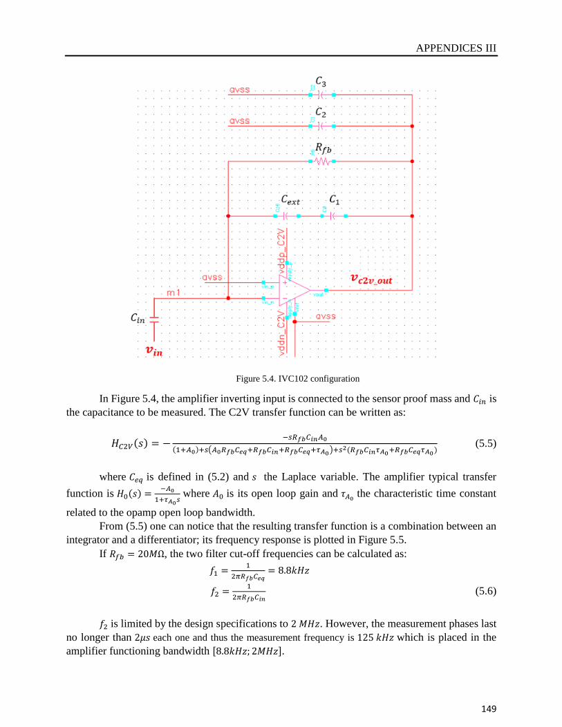
APPENDICES III
149
Figure 5.4. IVC102 configuration
In Figure 5.4, the amplifier inverting input is connected to the sensor proof mass and 𝐶𝑖𝑛 is
the capacitance to be measured. The C2V transfer function can be written as:
𝐻𝐶2𝑉(𝑠) = −−𝑠𝑅𝑓𝑏𝐶𝑖𝑛𝐴0
(1+𝐴0)+𝑠(𝐴0𝑅𝑓𝑏𝐶𝑒𝑞+𝑅𝑓𝑏𝐶𝑖𝑛+𝑅𝑓𝑏𝐶𝑒𝑞+𝜏𝐴0)+𝑠2(𝑅𝑓𝑏𝐶𝑖𝑛𝜏𝐴0+𝑅𝑓𝑏𝐶𝑒𝑞𝜏𝐴0) (5.5)
where 𝐶𝑒𝑞 is defined in (5.2) and 𝑠 the Laplace variable. The amplifier typical transfer
function is 𝐻0(𝑠) =−𝐴0
1+𝜏𝐴0𝑠 where 𝐴0 is its open loop gain and 𝜏𝐴0
the characteristic time constant
related to the opamp open loop bandwidth.
From (5.5) one can notice that the resulting transfer function is a combination between an
integrator and a differentiator; its frequency response is plotted in Figure 5.5.
If 𝑅𝑓𝑏 = 20𝑀Ω, the two filter cut-off frequencies can be calculated as:
𝑓1 =1
2𝜋𝑅𝑓𝑏𝐶𝑒𝑞= 8.8𝑘𝐻𝑧
𝑓2 =1
2𝜋𝑅𝑓𝑏𝐶𝑖𝑛 (5.6)
𝑓2 is limited by the design specifications to 2 𝑀𝐻𝑧. However, the measurement phases last
no longer than 2𝜇𝑠 each one and thus the measurement frequency is 125 𝑘𝐻𝑧 which is placed in the
amplifier functioning bandwidth [8.8𝑘𝐻𝑧; 2𝑀𝐻𝑧].
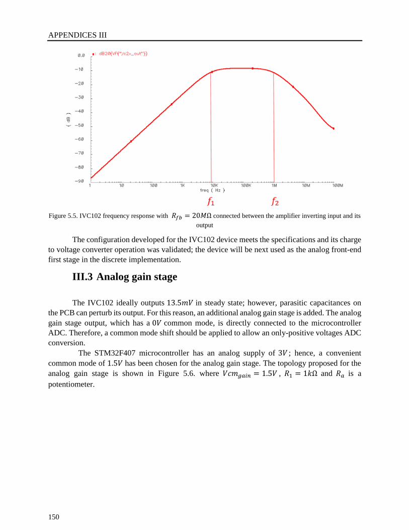
APPENDICES III
150
Figure 5.5. IVC102 frequency response with 𝑅𝑓𝑏 = 20𝑀Ω connected between the amplifier inverting input and its
output
The configuration developed for the IVC102 device meets the specifications and its charge
to voltage converter operation was validated; the device will be next used as the analog front-end
first stage in the discrete implementation.
III.3 Analog gain stage
The IVC102 ideally outputs 13.5𝑚𝑉 in steady state; however, parasitic capacitances on
the PCB can perturb its output. For this reason, an additional analog gain stage is added. The analog
gain stage output, which has a 0𝑉 common mode, is directly connected to the microcontroller
ADC. Therefore, a common mode shift should be applied to allow an only-positive voltages ADC
conversion.
The STM32F407 microcontroller has an analog supply of 3𝑉 ; hence, a convenient
common mode of 1.5𝑉 has been chosen for the analog gain stage. The topology proposed for the
analog gain stage is shown in Figure 5.6. where 𝑉𝑐𝑚𝑔𝑎𝑖𝑛 = 1.5𝑉 , 𝑅1 = 1𝑘Ω and 𝑅𝑎 is a
potentiometer.
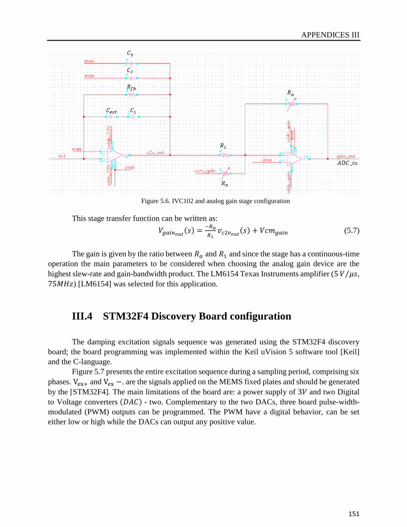
APPENDICES III
151
Figure 5.6. IVC102 and analog gain stage configuration
This stage transfer function can be written as:
𝑉𝑔𝑎𝑖𝑛𝑜𝑢𝑡(𝑠) =
−𝑅𝑎
𝑅1𝑣𝑐2𝑣𝑜𝑢𝑡
(𝑠) + 𝑉𝑐𝑚𝑔𝑎𝑖𝑛 (5.7)
The gain is given by the ratio between 𝑅𝑎 and 𝑅1 and since the stage has a continuous-time
operation the main parameters to be considered when choosing the analog gain device are the
highest slew-rate and gain-bandwidth product. The LM6154 Texas Instruments amplifier (5 𝑉 𝜇𝑠⁄ ,
75𝑀𝐻𝑧) [LM6154] was selected for this application.
III.4 STM32F4 Discovery Board configuration
The damping excitation signals sequence was generated using the STM32F4 discovery
board; the board programming was implemented within the Keil uVision 5 software tool [Keil]
and the C-language.
Figure 5.7 presents the entire excitation sequence during a sampling period, comprising six
phases. Vex+ and Vex −. are the signals applied on the MEMS fixed plates and should be generated
by the [STM32F4]. The main limitations of the board are: a power supply of 3𝑉 and two Digital
to Voltage converters (𝐷𝐴𝐶) - two. Complementary to the two DACs, three board pulse-width-
modulated (PWM) outputs can be programmed. The PWM have a digital behavior, can be set
either low or high while the DACs can output any positive value.
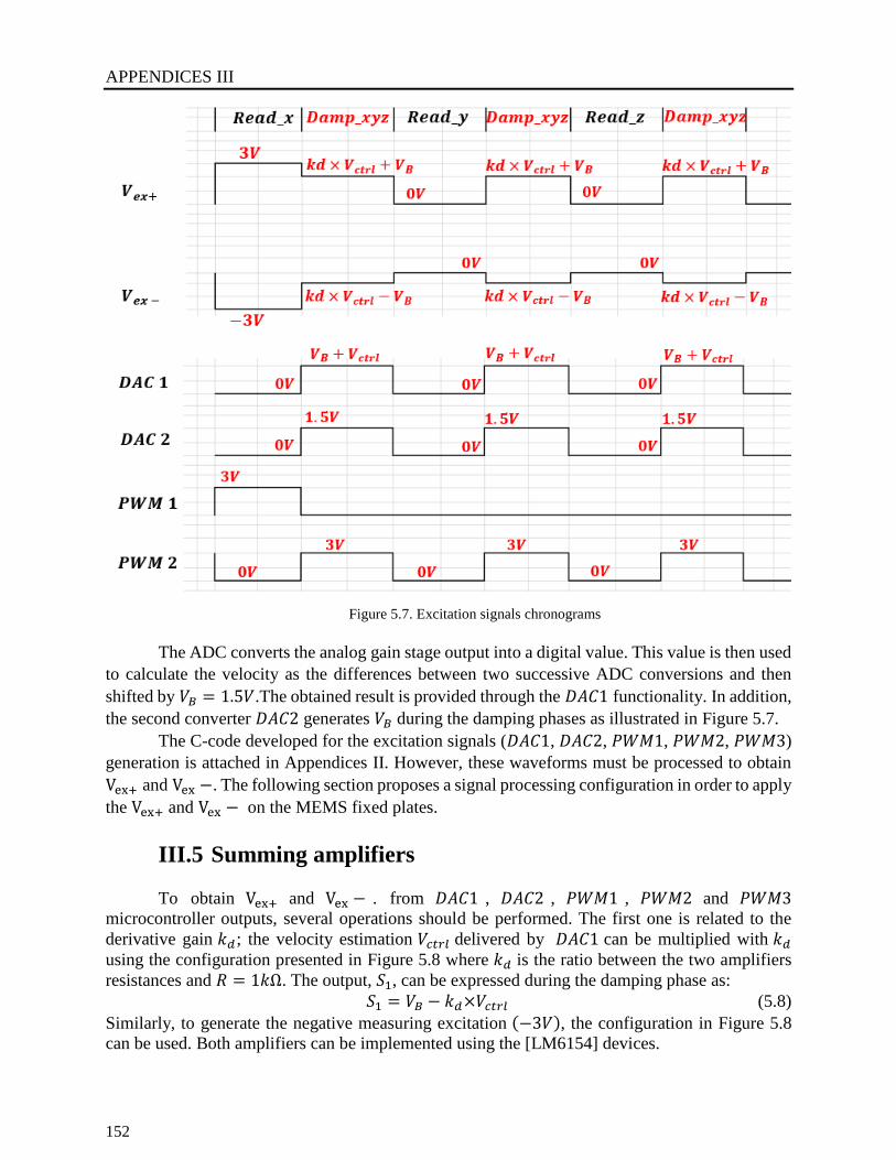
APPENDICES III
152
Figure 5.7. Excitation signals chronograms
The ADC converts the analog gain stage output into a digital value. This value is then used
to calculate the velocity as the differences between two successive ADC conversions and then
shifted by 𝑉𝐵 = 1.5𝑉.The obtained result is provided through the 𝐷𝐴𝐶1 functionality. In addition,
the second converter 𝐷𝐴𝐶2 generates 𝑉𝐵 during the damping phases as illustrated in Figure 5.7.
The C-code developed for the excitation signals (𝐷𝐴𝐶1, 𝐷𝐴𝐶2, 𝑃𝑊𝑀1, 𝑃𝑊𝑀2, 𝑃𝑊𝑀3)
generation is attached in Appendices II. However, these waveforms must be processed to obtain
Vex+ and Vex −. The following section proposes a signal processing configuration in order to apply
the Vex+ and Vex − on the MEMS fixed plates.
III.5 Summing amplifiers
To obtain Vex+ and Vex − . from 𝐷𝐴𝐶1 , 𝐷𝐴𝐶2 , 𝑃𝑊𝑀1 , 𝑃𝑊𝑀2 and 𝑃𝑊𝑀3
microcontroller outputs, several operations should be performed. The first one is related to the
derivative gain 𝑘𝑑; the velocity estimation 𝑉𝑐𝑡𝑟𝑙 delivered by 𝐷𝐴𝐶1 can be multiplied with 𝑘𝑑
using the configuration presented in Figure 5.8 where 𝑘𝑑 is the ratio between the two amplifiers
resistances and 𝑅 = 1𝑘Ω. The output, 𝑆1, can be expressed during the damping phase as: 𝑆1 = 𝑉𝐵 − 𝑘𝑑×𝑉𝑐𝑡𝑟𝑙 (5.8)
Similarly, to generate the negative measuring excitation (−3𝑉), the configuration in Figure 5.8
can be used. Both amplifiers can be implemented using the [LM6154] devices.
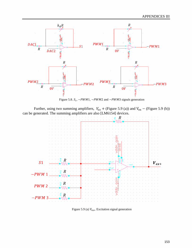
APPENDICES III
153
Figure 5.8. 𝑆1, −𝑃𝑊𝑀1, −𝑃𝑊𝑀2 and −𝑃𝑊𝑀3 signals generation
Further, using two summing amplifiers, 𝑉𝑒𝑥 + (Figure 5.9 (a)) and Vex − (Figure 5.9 (b))
can be generated. The summing amplifiers are also [LM6154] devices.
Figure 5.9 (a) Vex+ Excitation signal generation
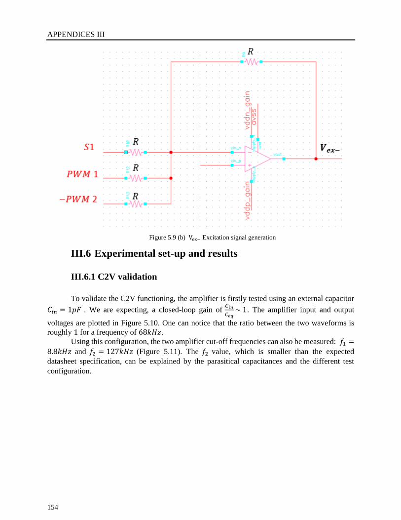
APPENDICES III
154
Figure 5.9 (b) Vex− Excitation signal generation
III.6 Experimental set-up and results
III.6.1 C2V validation
To validate the C2V functioning, the amplifier is firstly tested using an external capacitor
𝐶𝑖𝑛 = 1𝑝𝐹 . We are expecting, a closed-loop gain of 𝐶𝑖𝑛
𝐶𝑒𝑞~ 1. The amplifier input and output
voltages are plotted in Figure 5.10. One can notice that the ratio between the two waveforms is
roughly 1 for a frequency of 68𝑘𝐻𝑧.
Using this configuration, the two amplifier cut-off frequencies can also be measured: 𝑓1 =
8.8𝑘𝐻𝑧 and 𝑓2 = 127𝑘𝐻𝑧 (Figure 5.11). The 𝑓2 value, which is smaller than the expected
datasheet specification, can be explained by the parasitical capacitances and the different test
configuration.
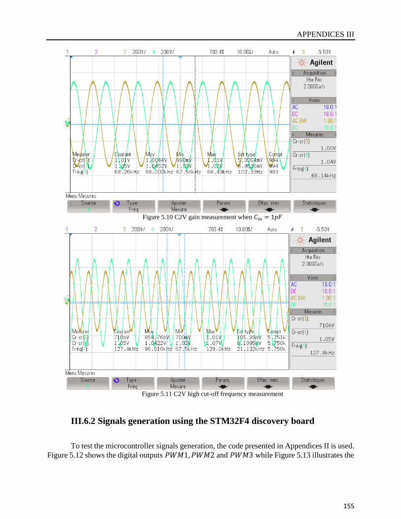
APPENDICES III
155
Figure 5.10 C2V gain measurement when 𝐶𝑖𝑛 = 1𝑝𝐹
Figure 5.11 C2V high cut-off frequency measurement
III.6.2 Signals generation using the STM32F4 discovery board
To test the microcontroller signals generation, the code presented in Appendices II is used.
Figure 5.12 shows the digital outputs 𝑃𝑊𝑀1, 𝑃𝑊𝑀2 and 𝑃𝑊𝑀3 while Figure 5.13 illustrates the
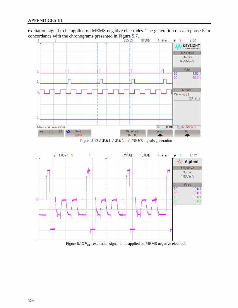
APPENDICES III
156
excitation signal to be applied on MEMS negative electrodes. The generation of each phase is in
concordance with the chronograms presented in Figure 5.7.
Figure 5.12 𝑃𝑊𝑀1, 𝑃𝑊𝑀2 and 𝑃𝑊𝑀3 signals generation
Figure 5.13 Vex− excitation signal to be applied on MEMS negative electrode
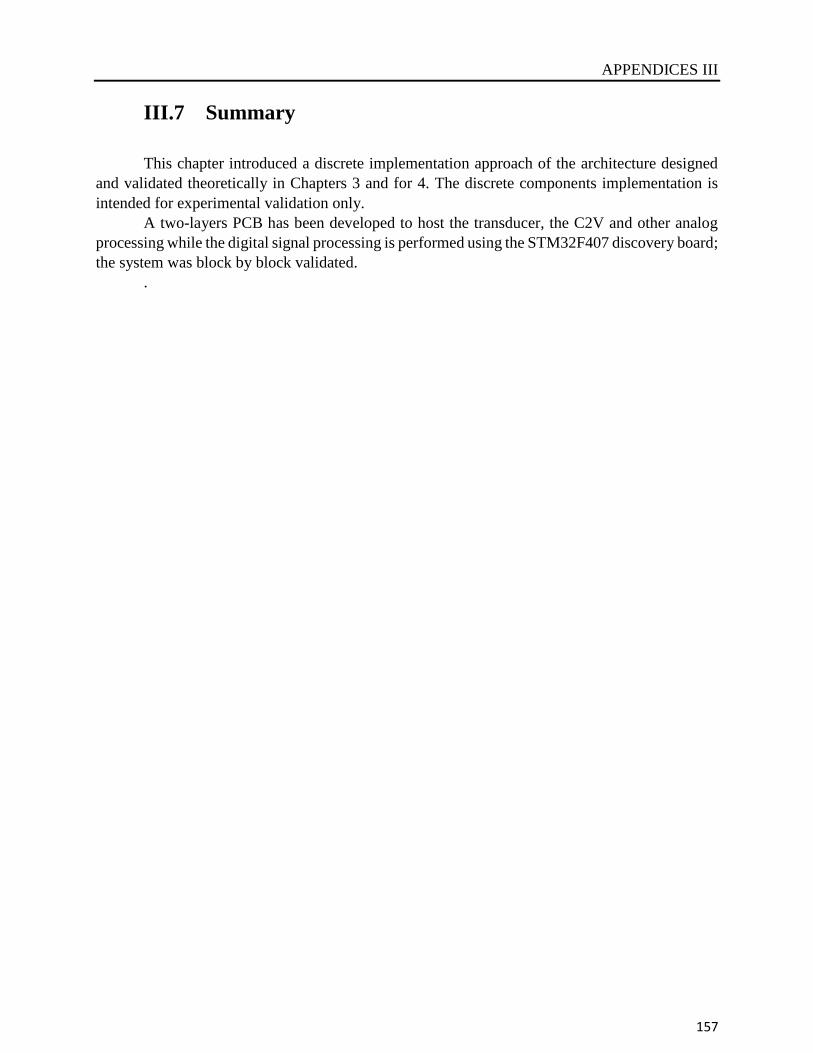
APPENDICES III
157
III.7 Summary
This chapter introduced a discrete implementation approach of the architecture designed
and validated theoretically in Chapters 3 and for 4. The discrete components implementation is
intended for experimental validation only.
A two-layers PCB has been developed to host the transducer, the C2V and other analog
processing while the digital signal processing is performed using the STM32F407 discovery board;
the system was block by block validated.
.

APPENDICES III
158
List of publications
1. Ciotirca Lavinia Elena, Thierry Cassagnes, Jérôme Enjalbert, Bernal Olivier, Hélène Tap
« A MICROELECTROMECHANICAL DEVICE AND A METHOD OF DAMPING A
MASS THEREOF » Freescale Semiconductor US Patent SA25488EC-WO, Filled March
1, 2016.
2. Ciotirca Lavinia, Olivier Bernal, Jérôme Enjalbert, Thierry Cassagnes, Hélène Tap. « 3-
axis high Q MEMS accelerometer with simultaneous damping control » NEWCAS June
26-29 2016, Vancouver, BC, Canada.
3. Chong Li, Ciotirca Lavinia Elena, Robert N. Dean, George T. Flowers « A MEMS PPA
Based Active Vibration Isolator » 12th International Conference and Exhibition on Device
Packaging, March 15-17, 2016 Austin, AZ, USA.
Recommended