Embed Size (px)
Citation preview
THÈSE
Pour l'obtention du grade deDOCTEUR DE L'UNIVERSITÉ DE POITIERS
École nationale supérieure d'ingénieurs (Poitiers)Laboratoire d'informatique et d'automatique pour les systèmes - LIAS
(Diplôme National - Arrêté du 7 août 2006)
École doctorale : Sciences et ingénierie pour l'information, mathématiques - S2IMSecteur de recherche : Electronique, microélectronique et nanoélectronique
Cotutelle : Universitatea politehnica (Bucarest)
Présentée par :Mihaela-Izabela Ionita
Contribution to the study of synchronized differentialoscillators used to controm antenna arrays
Directeur(s) de Thèse :Jean-Marie Paillot, David Cordeau, Mihai Iordache
Soutenue le 18 octobre 2012 devant le jury
Jury :
Président Marina Topa Domnule Profesor, Universitatii tehnice din Cluj Napoca, Romania
Rapporteur Farid Temcamani Professeur des Universités, ENSEA de Cergy-Pontoise
Rapporteur Lucian Mandache Domnule Profesor, Universitatea din Craiova, Romania
Membre Jean-Marie Paillot Professeur des Universités, Université de Poitiers
Membre David Cordeau Maître de conférences, Université de Poitiers
Membre Mihai Iordache Domnule Profesor, Universitatii Politehnice din Bucuresti, Romania
Pour citer cette thèse :Mihaela-Izabela Ionita. Contribution to the study of synchronized differential oscillators used to controm antennaarrays [En ligne]. Thèse Electronique, microélectronique et nanoélectronique. Poitiers : Université de Poitiers,2012. Disponible sur Internet <http://theses.univ-poitiers.fr>
THESE en cotutelle
Pour l’obtention du Grade de
DOCTEUR DE L’UNIVERSITE DE POITIERS (ECOLE SUPERIEURE d’INGENIEURS de POITIERS)
(Diplôme National - Arrêté du 7 août 2006)
Ecole Doctorale : Sciences et Ingénierie pour l’Information
et de
DOCTOR AL UNIVERSITATEA POLITEHNICA DIN BUCURE ŞTI Facultatea INGINERIE ELECTRICĂ
Catedra de ELECTROTEHNICĂ
Secteur de Recherche : ELECTRONIQUE, MICROELECTRONIQUE ET NANOELECTRONIQUE
Présentée par :
MIHAELA-IZABELA IONITA
************************
CONTRIBUTION TO THE STUDY OF SYNCHRONIZED DIFFERENT IAL
OSCILLATORS USED TO CONTROL ANTENNA ARRAYS
************************
Directeurs de Thèse : Jean-Marie PAILLOT, Mihai IORDACHE Co-directeur de Thèse : David CORDEAU
************************
Soutenue le 18 Octobre 2012
devant la Commission d’Examen
************************
JURY
Rapporteurs : Farid TEMCAMANI Professeur à l’ENSEA de Cergy-Pontoise Lucian MANDACHE Professeur à l’Université de Craiova Examinateurs : Marina TOPA Professeur à l’Université technique de Cluj Napoca Jean-Marie PAILLOT Professeur à l’Université de Poitiers Mihai IORDACHE Professeur à l’Université Polytechnique de Bucarest David CORDEAU Maître de conférences à l’Université de Poitiers


iii
ACKNOWLEDGEMENTS
First and foremost I want to thank my advisors Mr. Jean-Marie Paillot, Mr. David
Cordeau, professors at University of Poitiers, France and Mr. Mihai Iordache, professor at
University Politehnica of Bucharest. It has been an honor to work with you as a Ph.D.
student. I appreciate all your contributions of time, ideas, and funding to make my Ph.D.
experience productive and stimulating. I have learned so much from you, from figuring out
what research is, to choosing a research agenda, to learning how to present my work. Your
constructive criticism and collaboration have been tremendous assets throughout my Ph.D.
I would also like to thank the rest of my thesis committee for their support. Mr. Farid
Temcamani, professor at University of Cergy-Pontoise, Mr. Lucian Mandache, professor at
University of Craiova and Mrs. Marina Topa, professor at Technical University of Cluj-
Napoca, which provided me invaluable advice and comments on both my research and my
future research career plans. I would also like to thank to Mrs. Lucia Dumitriu, for her
support and encouragements.
I’ve been very lucky throughout most of my life as a Ph.D student, in that I’ve been
able to concentrate mostly on my research. This is due in a large part to the gracious support
of the team from LAII (Laboratoire d’Automatique et d’Informatique Industrielle) of
University of Poitiers, France. The team has been a source of friendships as well as good
advice and collaboration. I am especially grateful to Mr. Smail Bachir and Mr. Claude
Duvanaud, professors at University of Poitiers.
I would also like to express my thanks to the head of the LAII, Mr. Gerard
Champenois, for accepting me as Ph. D student in his laboratory and for the funding sources
that made my Ph.D. work possible in France.
I gratefully acknowledge the funding sources from University Politehnica of
Bucharest and I would also like to express my thanks to prof.dr.ing. Ecaterina Andronescu.
I’ve been fortunate to have a great group of friends that became a part of my life. Not
only are you the people I can discuss my research with and goof off with, but also you are
confidants who I can discuss my troubles with and who stand by me through thick and thin.
This, I believe, is the key to getting through a Ph.D. program – having good friends to have
fun with and complain to.

iv
Finally, I would like to dedicate this work to my family: my parents and my sister.
Without your unending support and love from childhood to now, I never would have made it
through this process or any of the tough times in my life. Thank you.
v
TABLE OF CONTENT
Introduction ………………………………………………………….. 1
Chapter I – Coupled-Oscillator Arrays – Application.………….. 4
1.1. Introduction...…………………………………………………... 5
1.2. Oscillator principle……...……………………………………... 6
1.2.1. The sinusoidal oscillator………………………….. 9
1.2.1.1. The RC oscillator…………………………... 10
1.2.1.2. The LC oscillator…………………………... 12
1.2.1.3. Crystal oscillator……………………........... 13
1.2.1.4. The Armstrong oscillator………………….. 14
1.2.1.5. The Hartley oscillator……………………… 15
1.2.1.6. The Colpitts oscillator……………………... 16
1.2.1.7. The Pierce oscillator……………………….. 16
1.2.1.8. The differential oscillator………………….. 17
1.2.1.9. The Van der Pol oscillator…....................... 19
1.3. State of the art of coupled oscillators theory………………….. 20
1.4. Applications: Beamsteering of antenna arrays………………... 22
1.4.1. Antenna arrays……………………………………. 23
1.4.1.1. Uniform linear network……………............ 24
1.4.1.2. Controlling the shape of the radiation pattern………………………………............ 26
1.4.1.2.1. Phase synthesis……………….. 27
1.4.1.2.2. Amplitude and phase synthesis 31
1.4.2. The control of the radiation pattern using coupled oscillators…………………………………………. 33
1.5. Conclusion……………………………………………………… 35

vi
Chapter II – Theoretical Analysis of Coupled Oscillators Applied to an Antenna Array……………………….. 36
2.1. Introduction…………………………………………………….. 37
2.2. Dynamics of two Van der Pol oscillators coupled through a resonant circuit…………………………………………………. 38
2.3. Dynamics of two Van der Pol oscillators coupled through a broad-band circuit……………………………………………… 48
2.4. New formulation of the equations describing the locked states of two Van der Pol coupled oscillators allowing a more accurate prediction of the amplitudes……………………….... 51
2.4.1. Two Van der Pol oscillators coupled through a resonant network……………………………………………. 51
2.4.2. Resistive coupling case…………………………… 60
2.5. New formulation of the equations describing the locked states of two Van der Pol oscillators allowing an easier numerical solving method…………………………………………………. 61
2.6. CAD tool “ASVAL”………………………………………….... 68
2.6.1. The objective of “ASVAL”………………………. 68
2.6.2. Variables estimation technique…………………... 71
2.6.3. Stability of synchronized states………………….. 72
2.7. The cartography of the synchronization area…………………. 74
2.8. Conclusion…………………………….……………………….. 77
Chapter III – Study and Analysis of an Array of Differential Oscillators and VCOs Coupled Through a Resistive Network………………………………………………… 79
3.1. Introduction…………………………………………………….. 80
3.2. Analysis and design of two differential oscillators coupled through a resistive network……………………………………. 81
3.2.1. RLC differential oscillator schematic…………. 81
3.2.2. The modeling of the differential oscillator as a 84
vii
Van der Pol oscillator
3.2.2.1. The modeling of the passive part………….. 84
3.2.2.2. The modeling of the active part…………… 85
3.2.2.3. Simulations of the Van der Pol oscillator…. 87
3.2.3. Two coupled differential Van der Pol oscillators.. 88
3.2.4. Two coupled differential oscillators……………... 93
3.2.5. Comparison between the theory, the Van der Pol model and the differential structure……………… 96
3.2.6. Study and analysis of the two coupled differential oscillators in the weak coupling case…………….. 100
3.2.7. Study and analysis of the two coupled differential oscillators in the strong coupling case…………… 103
3.3. Analysis and design of two VCOs coupled through a resistive network…...……………………………………………………..
106
3.3.1. Introduction……………………………………….. 106
3.3.2. The LC VCO architecture………………………… 109
3.3.2.1. The design of the passive part……………... 110
3.3.2.2. The design of the active part………………. 111
3.3.2.3. VCO simulation results……………………. 112
3.3.3. The modeling of a differential VCO as a differential Van der Pol oscillator………………... 115
3.3.3.1. The modeling of the passive part………….. 115
3.3.3.2. The modeling of the active part…………… 117
3.3.4. Two coupled differential VCOs………………….. 120
3.3.4.1. Study and analysis of two coupled differential VCOs of an optimal coupling case………………. 120
3.3.4.1.1. Study and analysis of two coupled differential VCOs using the state equation approach………………………….. 125
3.3.4.2. Study and analysis of two coupled differential 131
viii
VCOs in the weak coupling case………………….
3.3.4.3. Study and analysis of two coupled differential VCOs in the strong coupling case……………… 133
3.3.4.4. Study and analysis of the variation of the phase shift ∆φ versus the coupling resistor Rc 135
3.3.4.5. The effect of a mismatch between the two Rc on
the phase shift ∆φ…………………………………. 138
3.3.5. Four coupled differential VCOs………………….. 140
3.4. Conclusion.……………………………………………………... 142
Final conclusion.….………………………………………………….. 144
List of publications………………………………………………….. 150
Appendix A…………………………………………………………… 151
Appendix B…………………………………………………………… 156
References……………………………………………………………. 166
Abstract………………………………………………………………. 173

ix
x
LIST OF FIGURES
No. fig. Title of the figure Page
Figure 1.1 Block diagram of an array of N coupled oscillators…. 6
Figure 1.2 Linear model of an oscillator….…………………....... 7
Figure 1.3 Model of a one-port oscillator..………………………. 8
Figure 1.4 The block diagram of a typical feedback amplifier...... 10
Figure 1.5 The RC oscillator…………………………………..….. 10
Figure 1.6 The LC oscillator…………………………………..….. 12
Figure 1.7 Feedback signal coupling for the LC oscillators……... 13
Figure 1.8 The symbol and the equivalent circuit of a quartz crystal………………………………………………...... 13
Figure 1.9 (a) Series-fed Armstrong oscillator; (b) Shunt fed Armstrong oscillator………………………………….. 14
Figure 1.10 The Hartley oscillator…………................................... 15
Figure 1.11 The Colpitts oscillator………………………………… 16
Figure 1.12 A Pierce oscillator with PNP transistor in the common-base configuration…………………………... 17
Figure 1.13 Electronic structure of a differential oscillator………. 18
Figure 1.14 Electronic structure of a Van der Pol oscillator……… 20
Figure 1.15 Linear network scheme………………………..……… 25
Figure 1.16 The imposed sizes of the level and opening for the main and side lobes…………………………………… 27
Figure 1.17 The control on RF path………………….……………. 30
Figure 1.18 The architecture with polyphase oscillators represented here with four antennas………………….. 30
Figure 1.19 The architecture with four coupled VCOs…………… 31
Figure 1.20 Vector modulator architecture used on LO path……... 32
xi
Figure 1.21 Vector modulator architecture used on RF path.……. 32
Figure 1.22 Block diagram of an antenna array using coupled oscillators…………………………………………….... 34
Figure 2.1 Two Van der Pol oscillators coupled through a RLC circuit……………………………………………….…. 39
Figure 2.2 Van der Pol oscillator model……………………...….. 52
Figure 2.3 Two Van der Pol oscillators coupled through a series RLC circuit………………………...………………….. 53
Figure 2.4 The graphical representation of a synchronization area……...……………………………………………... 70
Figure 2.5 Two coupled differential Van der Pol oscillators……. 75
Figure 2.6 The cartographies of the phase shift ∆φ, the amplitudes A1 and A2 and the synchronization frequency fS of the coupled oscillators……………… 76
Figure 2.7 The cartography of the phase shift: example ∆φ = 42° 77
Figure 3.1 The schematic of the RLC differential oscillator…….. 81
Figure 3.2 a) The waveforms of the output voltage of the differential oscillator; b) The output spectrum………. 83
Figure 3.3 The identification of the Van der Pol passive part parameters……………………………………………... 85
Figure 3.4 The Van der Pol characteristic………………………... 86
Figure 3.5 The differential Van der Pol oscillator model with i = -av +bv3……………………………………………….. 87
Figure 3.6 Comparison between the output voltages of the differential oscillator and the differential Van der Pol oscillator model………………………………………..
88
Figure 3.7 Two coupled Van der Pol oscillators…………………. 88
Figure 3.8.a Two single-ended oscillators coupled through a resistor…………………………………………………. 89
Figure 3.8.b Two differential oscillators coupled through a resistor 90
xii
Figure 3.9 a) The waveforms of the output voltages of the coupled differential Van der Pol oscillators for
∆=7,4%; b) The output spectrum……………………... 92
Figure 3.10 Two differential oscillators coupled through a resistor 93
Figure 3.11 a) The waveforms of the output voltages of the coupled differential oscillators for ∆=7.4%; b) The output spectrum……………………………………….. 95
Figure 3.12 Cartography of the oscillators’ locked states provided by the CAD tool……………………………………….. 97
Figure 3.13 Waveforms of the output voltages of the two coupled differential NMOS oscillators, when ∆φ = 31.23° and A = 2.72 V 98
Figure 3.14 a) Comparison of the phase shift; b) Comparison of the amplitude………………………………………….. 99
Figure 3.15 The weak coupling case – a) Comparison of the phase shift; b) Comparison of the amplitude 101
Figure 3.16 The cartographies of the phase shift ∆φ, the amplitudes A1 and A2 and the synchronization frequency fs of the coupled oscillators for the weak coupling case………………………………………….. 103
Figure 3.17 The strong coupling case – a) Comparison of the phase shift; b) Comparison of the amplitude………… 104
Figure 3.18 The cartographies of the phase shift ∆φ, the amplitudes A1 and A2 and the synchronization frequency fs of the coupled oscillators for the strong coupling case………………………………………….. 105
Figure 3.19 The RLC NMOS differential oscillator: a)Comparison of ∆φ while changing L and C; b) Comparison of the amplitude while changing L and C…………………… 107
Figure 3.20 The Van der Pol oscillator: a) Comparison of ∆φ while changing L and C; b) Comparison of the amplitude while changing L and C…………………… 108
xiii
Figure 3.21 The LC VCO schematic………………………………. 109
Figure 3.22 a) Variation of C versus Vtune; b) Variation of Q versus Vtune…………………………………………… 111
Figure 3.23 The VCO oscillation frequency versus Vtune………... 112
Figure 3.24 The output power of the VCO………………………… 113
Figure 3.25 The output voltages of the VCO……………………… 113
Figure 3.26 Simulated phase noise of the VCO for a tuning voltage of 0.62 V……………………………………… 114
Figure 3.27 Simulated phase noise at 1 MHz versus tuning voltage…………………………………………………. 114
Figure 3.28 The identification of the parameters of the Van der Pol resonator…………………………………………... 116
Figure 3.29 The real and imaginary part of the two impedances Z11 and Z22……………………………………………... 117
Figure 3.30 The Van der Pol characteristic obtained for a VCO…. 118
Figure 3.31 The differential output voltage of a VCO at 5.89 GHz 119
Figure 3.32 The differential Van der Pol oscillator………………... 119
Figure 3.33 Two coupled differential VCOs………………………. 120
Figure 3.34 Two differential Van der Pol coupled oscillators……. 120
Figure 3.35 Cartography of the VCOs’ locked states provided by the CAD tool…………………………………………... 122
Figure 3.36 Waveforms of the output voltages of the two differential NMOS VCOs for ∆φ = 65.6° and A≈1.5 V 123
Figure 3.37 a) Comparison of the phase shift; b) Comparison of the amplitude………………………………………….. 124
Figure 3.38 Two differential Van der Pol oscillators coupled through a resistor with GNL = -a + buC1
2(t)…………... 126
Figure 3.39 The output voltages of two coupled differential Van der Pol oscillators obtained with Matlab for ∆φ = 75.6°, A = 1.35 V and fS = 5.89 GHz………………… 129
xiv
Figure 3.40 a) Comparison of the phase shift; b) Comparison of the amplitude………………………………………….. 130
Figure 3.41 The weak coupling case – a) Comparison of the phase shift; b) Comparison of the amplitude………………... 132
Figure 3.42 The cartographies of the phase shift ∆φ, the amplitudes A1 and A2 and the synchronization frequency fs of the coupled VCOs for the weak coupling case………………………………………….. 133
Figure 3.43 The strong coupling case – a) Comparison of the phase shift; b) Comparison of the amplitude………… 134
Figure 3.44 The cartographies of the phase shift ∆φ, the amplitudes A1 and A2 and the synchronization frequency fs of the coupled VCOs for the strong coupling case………………………………………….. 135
Figure 3.45 The variation of the phase shift versus Rc when f0 = 100 MHz………………………………………………. 137
Figure 3.46 The variation of the phase shift versus Rc when f0 = 200 MHz………………………………………………. 137
Figure 3.47 a) The variation of the phase shift for 5% mismatch; b) The variation of the amplitude for 5% mismatch…. 139
Figure 3.48 a) The variation of the phase shift for 7% mismatch; b) The variation of the amplitude for 7% mismatch…. 140
Figure 3.49 Schematic of four coupled VCOs…………………….. 141
Figure 3.50 Waveforms of the output voltages of the four
differential NMOS VCOs for ∆φ ≈ -37°…………….. 141

xv
LIST OF TABLES
No. table Title of the table Page
Table 1 The synchronization frequency, phase shift and amplitude obtained for two coupled differential Van der Pol oscillators……………………………………... 91
Table 2 The synchronization frequency, phase shift and amplitude obtained for two coupled differential oscillators……………………………………………… 94
Table 3 The varactor diode’s performances…………………... 111

1
INTRODUCTION
Introduction
2
Arrays of coupled oscillators offer a potentially useful technique for producing
higher powers at millimeter-wave frequencies with better efficiency than is possible with
conventional power-combining techniques. Another application is the beam steering of
antenna arrays. In this case, the radiation pattern of a phased antenna array is steered in a
particular direction by establishing a constant phase progression in the oscillator chain
which is obtained by detuning the free-running frequencies of the outermost oscillators in
the array. Moreover, it is shown that the resulting inter-stage phase shift is independent of
the number of oscillators in the array. Furthermore, synchronization phenomena in arrays
of coupled oscillators are very important models to describe various higher-dimensional
nonlinear phenomena in the field of natural science.
Many techniques have been used to analyse the behaviour of coupled oscillators for
many years such as time domain approaches or frequency domain approaches. Concerning
the last ones, R. York & al. made use of simple Van der Pol oscillators to model
microwave oscillators coupled through either a resistive network or a broad-band network.
Since these works are limited to cases where the coupling network bandwidth is much
greater than the oscillators’ bandwidth, he used more accurate approximations based on a
generalization of Kurokawa’s method to extend the study to the case of a narrow-band
circuit. This theory allows the equations for the amplitude and phase dynamics of two
oscillators coupled through many types of circuits to be derived. As a consequence, it
provides a full analytical formulation allowing to predict the performances of microwave
oscillator arrays. Unfortunately, it is shown that the theoretical limit of the phase shift that
can be obtained by slightly detuning the end elements of the array by equal amounts but in
opposite directions is only ±90°. Thus, it seems interesting to study and analyze the
behavior of an array of coupled differential oscillators or Voltage Controlled Oscillators
(VCOs) since, in this case, the theoretical limit of the phase shift is within 360° due to the
differential operation of the array, leading to an efficient beam-scanning architecture for
example. Furthermore, differential oscillators are widely used in high-frequency circuit
design due to their relatively good phase noise performances and ease of integration.
Due to these considerations, the aim of this work is to study and analyze the
behavior of coupled differential oscillators and VCOs used to control antenna arrays.

Introduction
3
In the first chapter, we will first remind the principle of an oscillator, including the
Van der Pol oscillator. Then, a state of the art of coupled-oscillator theory will be provided
followed by a brief presentation of antenna arrays theory and their applications in the
communication systems. Finally, few technical solutions to control the radiation pattern
will be presented, including the coupled oscillators approach.
In chapter 2, an overview over R. York’s theory giving the dynamics for two Van
der Pol oscillators coupled through a resonant network will be presented. Then, the case of
a broadband coupling circuit will be showed. Since the Van der Pol model used is too
simple and doesn’t allow an accurate prediction of the amplitudes, a new formulation of the
equations describing the locked states of these two coupled oscillators using an accurate
model allowing a good prediction of the amplitudes will be then described. Finally,
mathematical manipulations will be applied to the dynamic equations describing the locked
states of the coupled Van der Pol oscillators. A reduced system of equations with no
trigonometric aspects will be obtained, leading to the elaboration of a CAD tool that
provides, in a considerably short simulation time, the frequency locking region of two
differential oscillators coupled through a resistive network, in terms of the amplitudes of
their output signals and the phase shift between them.
The last chapter will be dedicated to the study and the analysis of an array of
differential oscillators and VCOs coupled through a broadband network. Hence, in the first
part of this chapter dealing with the analysis of two coupled differential oscillators, a
modeling procedure of the differential oscillator as a differential Van der Pol oscillator will
be presented. Then, the proposed CAD tool will be used in order to obtain the cartography
of the oscillators’ locked-states. The validation of the results provided by our CAD tool
will be showed by comparing them to the simulation results of the two coupled differential
oscillators obtained with Agilent’s ADS software for different cases of coupling strength.
Then, the same study will be performed for the case of two coupled differential Voltage
Controlled Oscillators (VCOs). Furthermore, the study of the variation of the phase shift
versus the coupling resistor will also be investigated as well as the effect of a mismatch
between the two coupling resistors on the phase shift. Finally, the behavior of four coupled
differential VCOs will be presented.
4
CHAPTER I
Coupled-Oscillator Arrays - Application
Chapter I – Coupled-Oscillator Arrays - Application
5
1.1. INTRODUCTION
During the past decade, arrays of coupled oscillators are the subject of increasing
research activity due to successful modeling of many diverse biological and physical
phenomena. Biological examples include swarms of synchronously flashing fireflies, the
coordinated firing of cardiac pacemaker cells, rhythmic spinal locomotion in vertebrates
and the synchronized activity of nerve cells in response to external stimuli. In physical
sciences, examples include oscillations in certain nonlinear chemical reactions, the
collective behavior of Josephson junction arrays and laser diode arrays [1]. Almost any
system of discrete or distinguishable behavior can be modeled by a system of coupled
oscillators.
In electronics, in particular, the synchronization behavior of oscillators has been
exploited in many relevant applications. Frequency locking effects have been used to
realize low-cost high-performance quadrature oscillators [2] or to reduce the effect of noise
[3]. Injection locking is the principle, which is at the basis of phase-locked loops (PLL)
circuits, furthermore it is employed to realize low-power consumption frequency dividers
for high-frequency applications [4]. Moreover, arrays of coupled oscillators offer a
potentially useful technique for producing higher powers at millimeter-wave frequencies
with better efficiency than is possible with conventional power-combining techniques [5,
6]. Another application is the beam steering of antenna arrays [7]. In this case, the radiation
pattern of a phased antenna array is steered in a particular direction by establishing a
constant phase progression in the oscillator chain. For a linear array presented in Figure
1.1, a phase shift ∆φ between adjacent elements results in steering the beam to an angle θ
off broadside, which is given by:
φ∆πλ
=θd
arcsin2
0 , (1.1)
where d is the distance separating two antennas and λ0 is the free-space wavelength
[8]. The required inter-stage phase shift can be obtained by detuning the free-running
frequencies of the outermost oscillators in the array [9, 10]. Moreover, it is shown that the
Chapter I – Coupled-Oscillator Arrays - Application
6
resulting inter-stage phase shift is independent of the number of oscillators in the array [1,
11, 12].
Figure 1.1 – Block diagram of an array of N coupled oscillators
In this chapter we will first remind the principle of an oscillator, where different
types of sinusoidal oscillators will be presented including the differential and Van der Pol
oscillators. Then, a state of art of coupled-oscillator theory will be provided followed by a
brief presentation of antenna arrays theory and their applications in the communication
system. Finally, few technical solutions to control the radiation pattern will be presented,
including the coupled oscillators approach.
1.2. OSCILLATOR PRINCIPLE
An oscillator is usually represented as a closed loop system. In Figure 1.2, we can
see a linear model of an oscillator, where A(jω) represents the transfer function of the
active element of the oscillator, and B(jω) represents the transfer function of the passive
part of the reaction, which gives the selection and stability of the oscillation frequency.
This passive part is represented by the resonator.
Chapter I – Coupled-Oscillator Arrays - Application
7
Figure 1.2 - Linear model of an oscillator.
The transfer function of this system can be written as follows:
ω) ω1
ω
ω
ω
) B ( j - A ( j
)A ( j
) ( jV
) ( j V
e
s = . (1.2)
Considering this expression, there is a pulsation, ω0, for which: Vs(jω0) ≠ 0 whereas
Ve(jω0) = 0; this pulsation must fulfill the relation A(jω0) .B(jω0) = 1.
Therefore, the oscillation conditions, known as Barkhausen, are written as follows:
==
π2ωω
1ωω
00
00
k ) ) .B ( j j Arg ( A (
) ) .B ( j A ( j (1.3)
where k ∈ N.
Therefore, in steady state, the module of the opened loop gain must be equal to one
and the total phase shift must be zero or 2kπ.
An oscillator circuit can also be represented by a nonlinear impedance, ZNL(I, ω),
which represents the active part of the oscillator, in parallel with the equivalent impedance
of the resonator, ZR(ω), as shown in Figure 1.3.
Chapter I – Coupled-Oscillator Arrays - Application
8
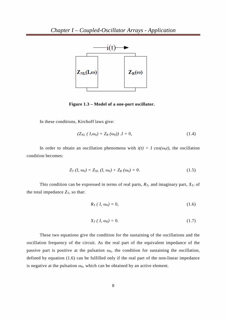
Figure 1.3 – Model of a one-port oscillator.
In these conditions, Kirchoff laws give:
(ZNL ( I,ω0) + ZR (ω0)) .I = 0, (1.4)
In order to obtain an oscillation phenomena with i(t) = I cos(ω0t), the oscillation
condition becomes:
ZT (I, ω0) = ZNL (I, ω0) + ZR (ω0) = 0. (1.5)
This condition can be expressed in terms of real parts, RT, and imaginary part, XT, of
the total impedance ZT, so that:
RT ( I, ω0) = 0, (1.6)
XT ( I, ω0) = 0. (1.7)
These two equations give the condition for the sustaining of the oscillations and the
oscillation frequency of the circuit. As the real part of the equivalent impedance of the
passive part is positive at the pulsation ω0, the condition for sustaining the oscillation,
defined by equation (1.6) can be fulfilled only if the real part of the non-linear impedance
is negative at the pulsation ω0, which can be obtained by an active element.
Chapter I – Coupled-Oscillator Arrays - Application
9
Oscillators are classified in accordance with the waveforms they produce and the
circuitry required for producing the desired oscillations, as presented in [13]:
The sinusoidal oscillator - the output voltage is sinusoidal;
The non-sinusoidal oscillator - the output voltage is non-sinusoidal but it has
triangular, square and saw tooth waveforms.
1.2.1. The Sinusoidal Oscillator
A sinusoidal oscillator is an oscillator that produces a sine-wave output signal. An
ideal oscillator should produce an output signal with constant amplitude with no variation
in frequency. A practical oscillator cannot have these criteria, the degree to which the ideal
is approached depends on the class of amplifier operation, amplifier characteristics,
frequency stability, and amplitude stability. Sinusoidal oscillators generate signals ranging
from low audio frequencies to ultrahigh radio and microwave frequencies.
The sinusoidal oscillators are classified as follows:
• RC oscillators;
• LC oscillators;
• the crystal-controlled oscillator.
Many low-frequency oscillators use resistors and capacitors to form their frequency-
determining networks and are referred to as RC oscillators. These are used in the audio-
frequency range.
The LC oscillators are commonly used for the higher radio frequencies. They are not
suitable for use as extremely low-frequency oscillators because the inductors and
capacitors would be large in size, heavy, and costly to manufacture.
The third category of sinusoidal oscillator is the crystal-controlled oscillator. The
crystal-controlled oscillator provides excellent frequency stability and is used from the
middle of the audio range through the radio frequency range.
Chapter I – Coupled-Oscillator Arrays - Application
10
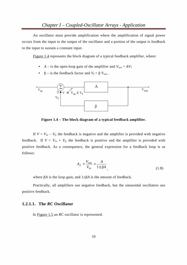
An oscillator must provide amplification where the amplification of signal power
occurs from the input to the output of the oscillator and a portion of the output is feedback
to the input to sustain a constant input.
Figure 1.4 represents the block diagram of a typical feedback amplifier, where:
• A – is the open-loop gain of the amplifier and Vout = AV;
• β – is the feedback factor and Vf = β Vout .
Figure 1.4 – The block diagram of a typical feedback amplifier.
If V = Vin – Vf, the feedback is negative and the amplifier is provided with negative
feedback. If V = Vin + Vf, the feedback is positive and the amplifier is provided with
positive feedback. As a consequence, the general expression for a feedback loop is as
follows:
A
A
V
VA
in
outf
β1±==
, (1.8)
where βA is the loop gain, and 1±βA is the amount of feedback.
Practically, all amplifiers use negative feedback, but the sinusoidal oscillators use
positive feedback.
1.2.1.1. The RC Oscillator
In Figure 1.5 an RC oscillator is represented.
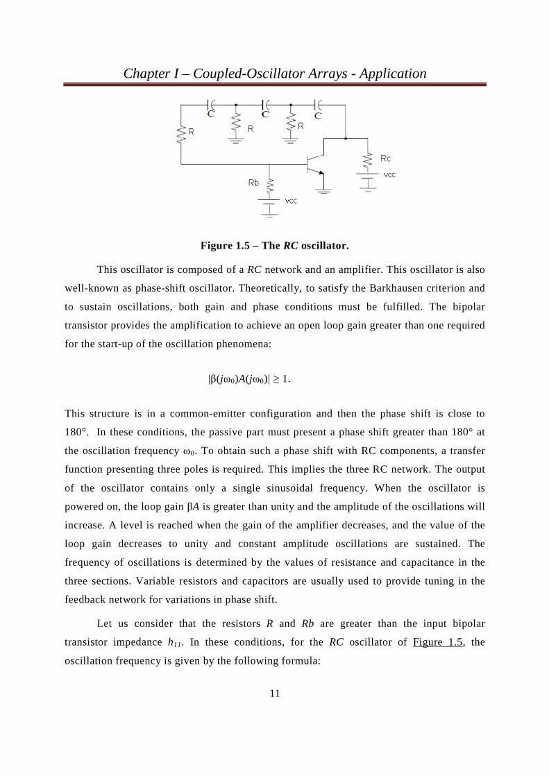
Chapter I – Coupled-Oscillator Arrays - Application
11
Figure 1.5 – The RC oscillator.
This oscillator is composed of a RC network and an amplifier. This oscillator is also
well-known as phase-shift oscillator. Theoretically, to satisfy the Barkhausen criterion and
to sustain oscillations, both gain and phase conditions must be fulfilled. The bipolar
transistor provides the amplification to achieve an open loop gain greater than one required
for the start-up of the oscillation phenomena:
|β(jω0)A(jω0)| ≥ 1.
This structure is in a common-emitter configuration and then the phase shift is close to
180°. In these conditions, the passive part must present a phase shift greater than 180° at
the oscillation frequency ω0. To obtain such a phase shift with RC components, a transfer
function presenting three poles is required. This implies the three RC network. The output
of the oscillator contains only a single sinusoidal frequency. When the oscillator is
powered on, the loop gain βA is greater than unity and the amplitude of the oscillations will
increase. A level is reached when the gain of the amplifier decreases, and the value of the
loop gain decreases to unity and constant amplitude oscillations are sustained. The
frequency of oscillations is determined by the values of resistance and capacitance in the
three sections. Variable resistors and capacitors are usually used to provide tuning in the
feedback network for variations in phase shift.
Let us consider that the resistors R and Rb are greater than the input bipolar
transistor impedance h11. In these conditions, for the RC oscillator of Figure 1.5, the
oscillation frequency is given by the following formula:
Chapter I – Coupled-Oscillator Arrays - Application
12
R
RRC
oL4
6
1
+=ω
(1.9)
In general, for an RC phase-shift oscillator, the frequency of oscillation (resonant
frequency) can be approximated with the following relation:
nRC 2
1ω0 = , (1.10)
where n is the number of RC sections.
1.2.1.2. The LC Oscillator
The LC oscillators use resonant circuits. A resonant circuit stores energy alternately
in the inductor and capacitor. However, every circuit contains some resistance and this
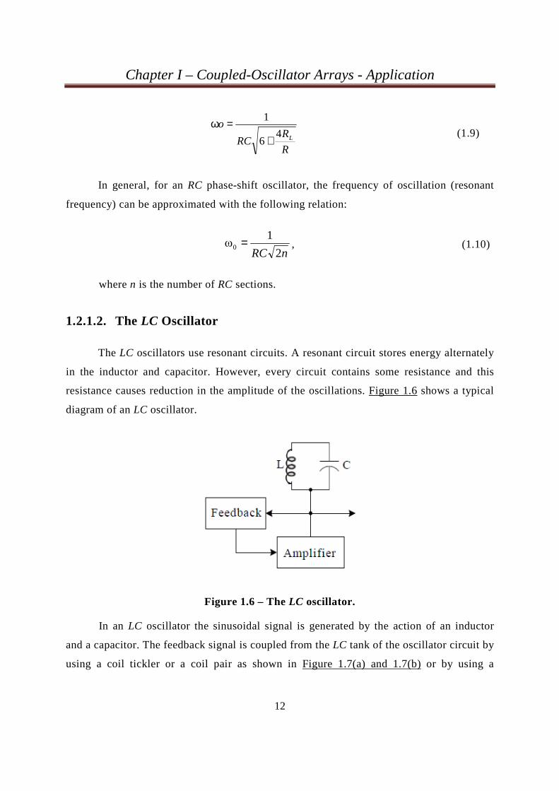
resistance causes reduction in the amplitude of the oscillations. Figure 1.6 shows a typical
diagram of an LC oscillator.
Figure 1.6 – The LC oscillator.
In an LC oscillator the sinusoidal signal is generated by the action of an inductor
and a capacitor. The feedback signal is coupled from the LC tank of the oscillator circuit by
using a coil tickler or a coil pair as shown in Figure 1.7(a) and 1.7(b) or by using a
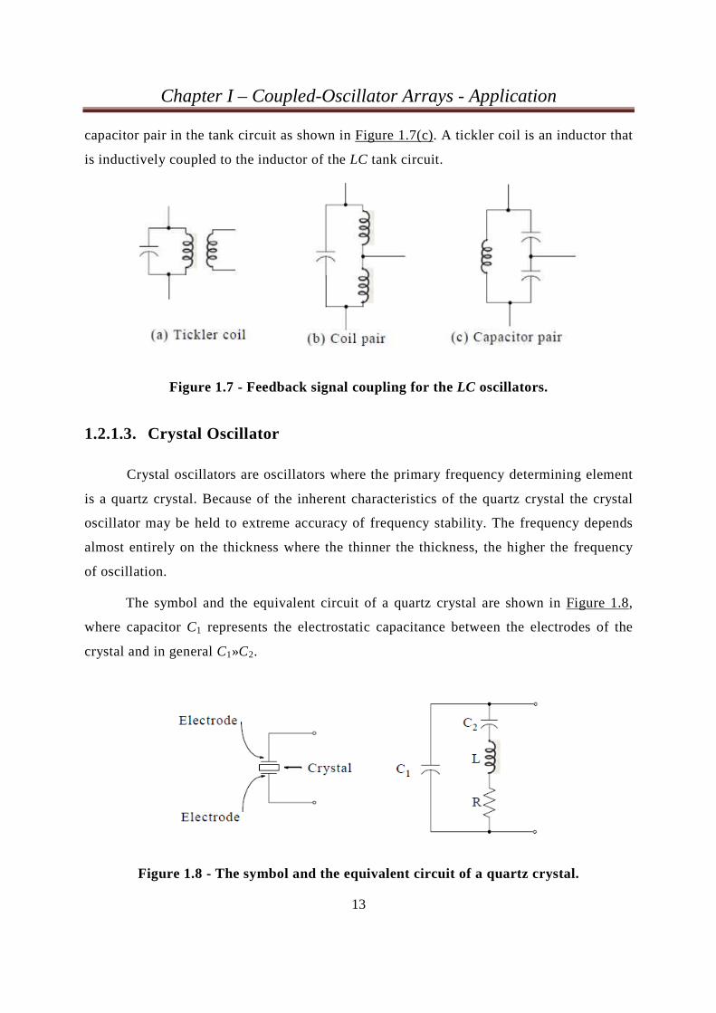
Chapter I – Coupled-Oscillator Arrays - Application
13
capacitor pair in the tank circuit as shown in Figure 1.7(c). A tickler coil is an inductor that
is inductively coupled to the inductor of the LC tank circuit.
Figure 1.7 - Feedback signal coupling for the LC oscillators.
1.2.1.3. Crystal Oscillator
Crystal oscillators are oscillators where the primary frequency determining element
is a quartz crystal. Because of the inherent characteristics of the quartz crystal the crystal
oscillator may be held to extreme accuracy of frequency stability. The frequency depends
almost entirely on the thickness where the thinner the thickness, the higher the frequency
of oscillation.
The symbol and the equivalent circuit of a quartz crystal are shown in Figure 1.8,
where capacitor C1 represents the electrostatic capacitance between the electrodes of the
crystal and in general C1»C2.
Figure 1.8 - The symbol and the equivalent circuit of a quartz crystal.
Chapter I – Coupled-Oscillator Arrays - Application
14
The available power is limited by the heat the crystal will withstand without
fracturing. The amount of heating is dependent upon the amount of current that can safely
pass through a crystal and this current may be in the order of 50 to 200 milliamperes.
Accordingly, temperature compensation must be applied to crystal oscillators to improve
thermal stability of the crystal oscillator.
Crystal oscillators are used in applications where frequency accuracy and stability
are of outmost importance such as broadcast transmitters and radar. The frequency stability
of crystal-controlled oscillators depends on the quality factor Q. The Q of a crystal may
vary from 10,000 to 100,000.
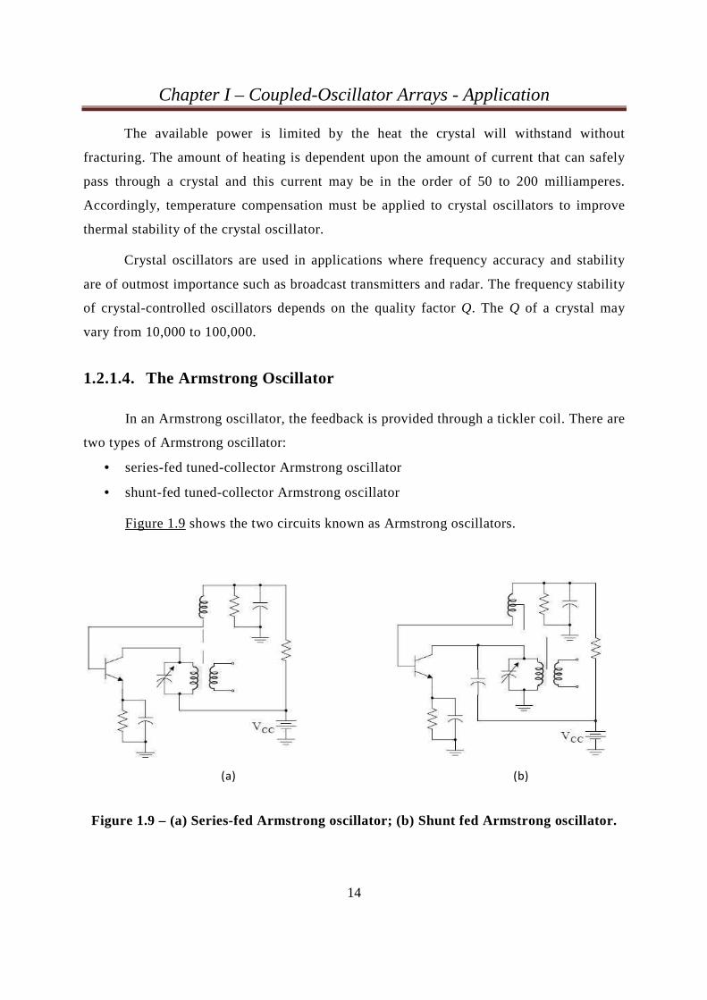
1.2.1.4. The Armstrong Oscillator
In an Armstrong oscillator, the feedback is provided through a tickler coil. There are
two types of Armstrong oscillator:
• series-fed tuned-collector Armstrong oscillator
• shunt-fed tuned-collector Armstrong oscillator
Figure 1.9 shows the two circuits known as Armstrong oscillators.
(a) (b)
Figure 1.9 – (a) Series-fed Armstrong oscillator; (b) Shunt fed Armstrong oscillator.
Chapter I – Coupled-Oscillator Arrays - Application
15
The series-fed tuned-collector Armstrong oscillator is so-called because the power
supply voltage Vcc supplied to the transistor is through the tank circuit. The shunt-fed
tuned-collector Armstrong oscillator is so-called because the power supply voltage Vcc
supplied to the transistor is through a path parallel to the tank circuit.
For both types of Armstrong oscillators, the power through Vcc is supplied to the
transistor and the tank circuit begins to oscillate.
The transistor conducts for a short period of time and returns sufficient energy to the
tank circuit to ensure a constant amplitude output signal.
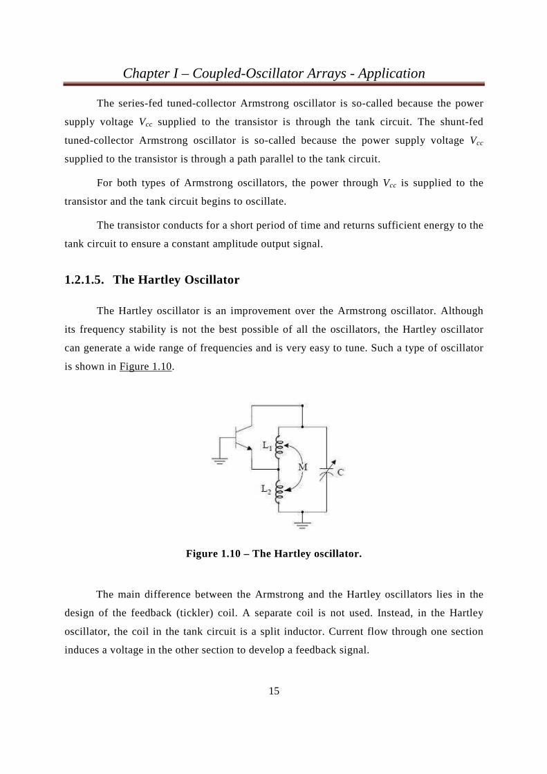
1.2.1.5. The Hartley Oscillator
The Hartley oscillator is an improvement over the Armstrong oscillator. Although
its frequency stability is not the best possible of all the oscillators, the Hartley oscillator
can generate a wide range of frequencies and is very easy to tune. Such a type of oscillator
is shown in Figure 1.10.
Figure 1.10 – The Hartley oscillator.
The main difference between the Armstrong and the Hartley oscillators lies in the
design of the feedback (tickler) coil. A separate coil is not used. Instead, in the Hartley
oscillator, the coil in the tank circuit is a split inductor. Current flow through one section
induces a voltage in the other section to develop a feedback signal.
Chapter I – Coupled-Oscillator Arrays - Application
16
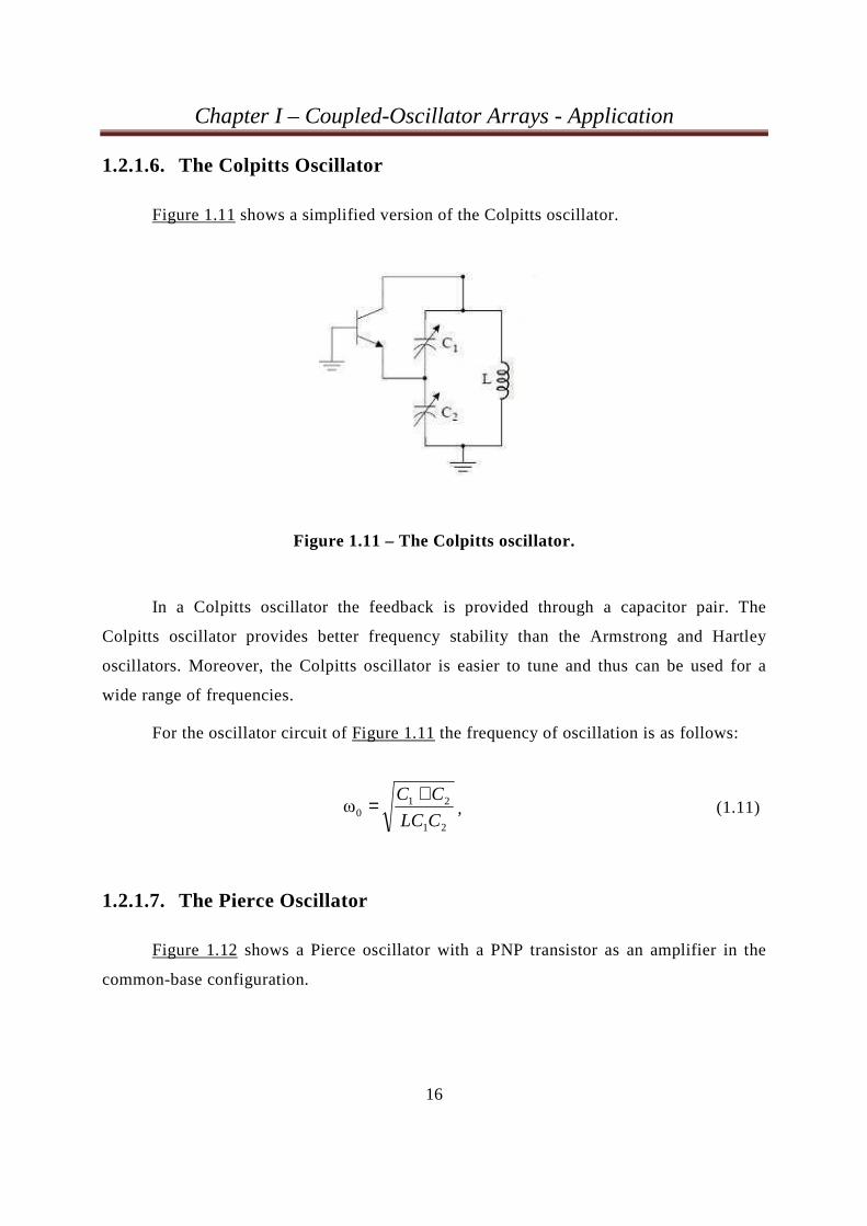
1.2.1.6. The Colpitts Oscillator
Figure 1.11 shows a simplified version of the Colpitts oscillator.
Figure 1.11 – The Colpitts oscillator.
In a Colpitts oscillator the feedback is provided through a capacitor pair. The
Colpitts oscillator provides better frequency stability than the Armstrong and Hartley
oscillators. Moreover, the Colpitts oscillator is easier to tune and thus can be used for a
wide range of frequencies.
For the oscillator circuit of Figure 1.11 the frequency of oscillation is as follows:
21
210ω CLC
CC += , (1.11)
1.2.1.7. The Pierce Oscillator
Figure 1.12 shows a Pierce oscillator with a PNP transistor as an amplifier in the
common-base configuration.
Chapter I – Coupled-Oscillator Arrays - Application
17
Figure 1.12 – A Pierce oscillator with PNP transistor in the common-base
configuration.
The Pierce oscillator is a modified Colpitts oscillator that uses a crystal as a
parallel-resonant circuit and for this reason is often referred to as crystal-controlled Pierce
oscillator.
In the oscillator circuit of Figure 1.12, feedback is provided from the collector to the
emitter of the transistor through capacitor C1 and resistors R1, RB, and RC are used to
establish the proper bias conditions. Besides the crystal, the frequency of oscillation is also
determined by the settings of the variable capacitors CE and CB.
1.2.1.8. The differential oscillator
Like the previous architectures, this type of oscillator presents a structure that
resonates at a frequency for which the losses are compensated by the active part, [14].
Thus, this resistance Rp is in parallel with a structure that can present a negative resistance.
In steady state, to sustain the oscillation, the negative resistance must be equal to the losses
resistance of the resonator. Usually, the negative resistance is represented by an element or
an active circuit (a structure based on transistors), as shown in Figure 1.13.
The output voltage between the points vx and vy is as follows:
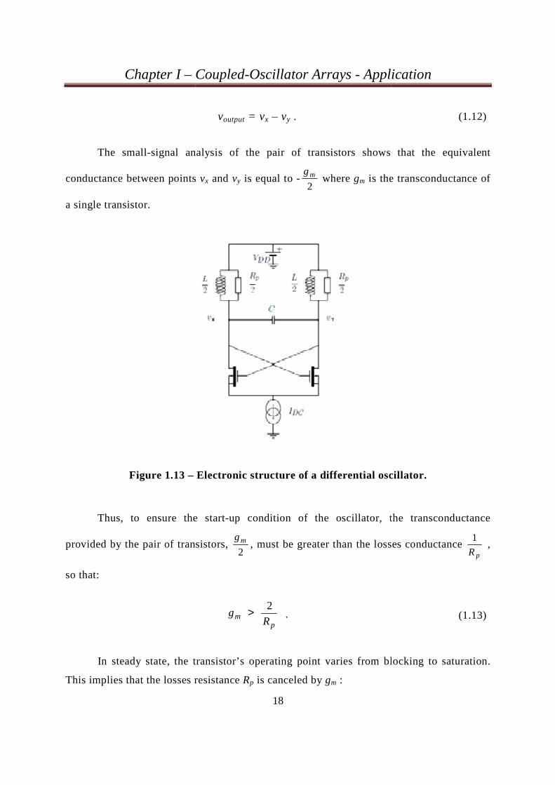
Chapter I – C
The small-signal ana
conductance between points
a single transistor.
Figure 1.13 –
Thus, to ensure the
provided by the pair of trans
so that:
In steady state, the tr
This implies that the losses r
Coupled-Oscillator Arrays - Appli
18
voutput = vx – vy .
analysis of the pair of transistors shows
ts vx and vy is equal to -2mg
where gm is the
Electronic structure of a differential osc
he start-up condition of the oscillator, th
ansistors, 2mg
, must be greater than the losse
pm R
g2> .
transistor’s operating point varies from blo
s resistance Rp is canceled by gm :
plication
(1.12)
s that the equivalent
the transconductance of
scillator.
the transconductance
sses conductance pR
1 ,
(1.13)
blocking to saturation.

Chapter I – Coupled-Oscillator Arrays - Application
19
pm R
g1−= . (1.14)
The problem of oscillation start-up is a critical problem in oscillators design.
Equations (1.13) and (1.14) indicate that the transistors must be oversized. Moreover,
because we can’t know precisely Rp, generally, the transistors have their transconductance
three or four times greater than that required in steady state.
The amplitude of the output voltage for this type of oscillator can be calculated
according to the limits of the transistor’s operating point. If one transistor of the
differential pair is off and the other is saturated, then, all the current IDC is flowing in this
latter. In this case we have:
=−
=
DCp
yDD
DDx
IR
v V
V v
2
. (1.15)
And the amplitude is:
DCp
yx IR
v v A 2
=−= .
(1.16)
1.2.1.9. The Van der Pol oscillator
The Van der Pol oscillator is an oscillator with nonlinear damping governed by the
second-order differential equation:
0 1 ε 2 =+−− xx)x(x , (1.17)
where:
• ε - is a positive constant, which measures the degree of linearity of the system;
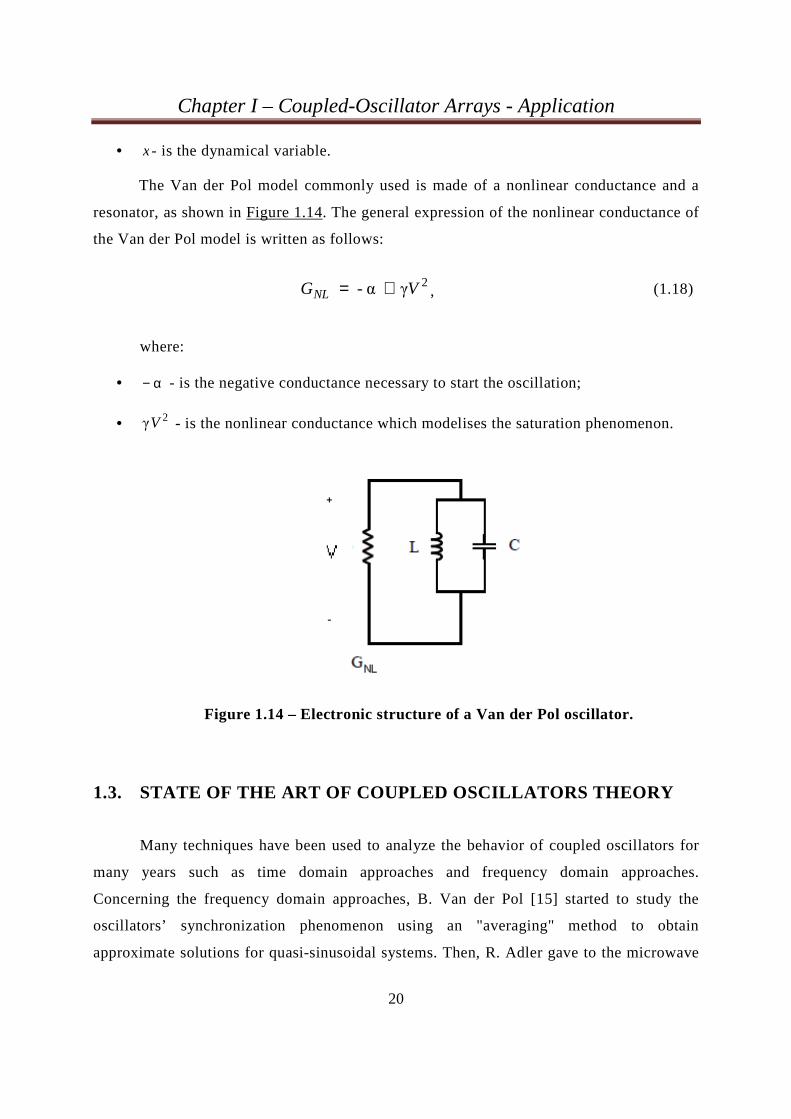
Chapter I – Coupled-Oscillator Arrays - Application
20
• x- is the dynamical variable.
The Van der Pol model commonly used is made of a nonlinear conductance and a
resonator, as shown in Figure 1.14. The general expression of the nonlinear conductance of
the Van der Pol model is written as follows:
2γα V - GNL += , (1.18)
where:
• α− - is the negative conductance necessary to start the oscillation;
• 2 γV - is the nonlinear conductance which modelises the saturation phenomenon.
Figure 1.14 – Electronic structure of a Van der Pol oscillator.
1.3. STATE OF THE ART OF COUPLED OSCILLATORS THEORY
Many techniques have been used to analyze the behavior of coupled oscillators for
many years such as time domain approaches and frequency domain approaches.
Concerning the frequency domain approaches, B. Van der Pol [15] started to study the
oscillators’ synchronization phenomenon using an "averaging" method to obtain
approximate solutions for quasi-sinusoidal systems. Then, R. Adler gave to the microwave
Chapter I – Coupled-Oscillator Arrays - Application
21
oscillator analysis a more physical basis defining the phase dynamic equation of an
oscillator under the influence of an injected signal [16]. This was sustained by K.
Kurokawa who derived the dynamic equations for both the amplitude and phase [17],
providing a pragmatic understanding of coupled microwave oscillators. In R. York’s
previous works, coupled microwave oscillators have been modeled as simple single-ended
Van der Pol oscillators coupled through either a resistive network or a broad-band network
[1, 11, 18]. Unfortunately, this works are limited to the cases when the coupling network
bandwidth is much greater than the oscillators’ bandwidth. In these conditions, a
generalization of Kurokawa’s method [17] was used to extend the study to a narrow-band
circuit allowing the equations for the amplitude and phase dynamics of two oscillators
coupled through many types of circuits to be derived [19]. Since these works, only few
papers present new techniques for the analysis of coupled-oscillator arrays in the frequency
domain [20, 21, 22]. In [22], a semi-analytical formulation is presented for the design of
coupled oscillator systems, avoiding the computational expensiveness of a full harmonic
balance synthesis presented in [20] and [21]. In [23], a simplified closed-form of the semi-
analytical formulation proposed in [22] for the optimized design of coupled-oscillator
systems is presented. Nevertheless, even if this new semi-analytical formulation allows a
good prediction of the coupled oscillator solution, it is only valid for the weak coupling
case.
Now, concerning the time domain approaches [24-29], among other, D. Aoun and
D.A. Linkens studied in [24] nonlinear oscillators used in bioelectronics applications, in
particular, towards the electrical activity of the mammalian gastro-intestinal tract. This
activity known as “slow-waves” has been extensively modeled using nonlinear oscillatory
dynamics. Therefore, they applied a matrix extension of the Krylov-Bogolioubov
linearization technique to a wide range of structures comprising chains, arrays, rings and
tubes. Unfortunately, it has been demonstrated that this technique produces complicated
stability criteria for the existence of stable limit cycles. Hence, they decided to engineer a
CAD package which solves these criteria for the structures mentioned above with an
arbitrary number of either third or fifth power conductance Van der Pol oscillators coupled
mutually. Later on, Chai Wah Wu and Leon O. Chua demonstrated in [25] how an array of
resistively coupled identical oscillators can be synchronized if the coupling conductances
Chapter I – Coupled-Oscillator Arrays - Application
22
are large enough. To do so, they used algebraic graph theory to derive sufficient conditions
for an array of resistively coupled nonlinear oscillators to synchronize. These conditions
are derived, in fact, from the connectivity graph, which describes how the oscillators are
connected. Moreover, they showed that the upper bound on the coupling conductance
required for synchronization for arbitrary graphs, is in order of n2, where n is the number of
oscillators. In [26], P. Maffezoni studies the synchronization phenomenon of the weakly
coupled oscillators using a phase-domain macromodel based on perturbation projection
vector that describes the linear periodically time-varying behavior of an oscillator in the
neighbor of its stable limit cycle. Using this method, the mutual locking range and the
common locking frequency of the locked oscillators could be predicted with great
precision. The reliability and accuracy of the method have been demonstrated also when
the mutual coupling results in an anomalous synchronization frequency. Furthermore, in
this way Maffezoni could estimate, by means of closed-form expressions, the mutual
pulling effects that arise between two self-sustained oscillators in the presence of weak
interactions.
Nevertheless, even if the time domain approaches offer a good prediction of the
coupled oscillator solution, the frequency domain approaches are less complex and more
preferred in the design of RF and microwave coupled oscillators. For instance, R. York’s
theory [19] provides a full analytical formulation allowing to predict the performances of
microwave oscillator arrays for both weak and strong coupling.
1.4. APPLICATIONS: BEAMSTEERING OF ANTENNA ARRAYS
Mobile communications are the subject of increasing research activity covering
many technical areas. Worldwide activities in this growing industry are perhaps an
indication of its importance.
An application of antenna arrays has been suggested in the recent years for mobile
communication systems in order to solve the problem of limited bandwidth of the channel,
and therefore, to satisfy the increasing demands for a large number of mobile
communication channels [30, 31]. Antenna arrays have many other advantages, in fact,
Chapter I – Coupled-Oscillator Arrays - Application
23
they contribute to the improving of the communication system performances while
increasing the channel capacity, providing a wider band of coverage, and minimizing the
multipath fading and also the interference between channels. Beside the advantages
mentioned in this paragraph, the two properties below also describe a few assets of antenna
arrays:
− The decrease of the electromagnetic pollution: the shape of the radiation pattern
can be optimized in order to reduce the side lobes. Similarly, the radiation pattern
can be orientated in the desired direction, and therefore any radiations in useless
directions are minimized.
− A better quality of the transmission / reception: the emitted power can be focused
in the desired direction and therefore the wasted power in useless directions is
reduced. One of the advantages resulting from this decrease is also the distribution
of the power on all power amplifiers constituting the transmission network.
Similarly, for the reception, the noise provided by the interfering signals is
minimized, leading to a reduced Bit Error Rate (BER), which is the priority of any
transmission architecture.
Thus, antenna arrays are essential to increase the efficiency of mobile
communications systems. For the transport area, these devices are installed on vehicles,
boats, planes, satellites and base stations in order to fulfill the channel requirements for this
service.
1.4.1. Antenna Arrays
An antenna array is defined as a set of N radiating elements distributed in space.
The amplitude and/or phase of the signal injected into each of these antennas can be
commanded so that it can control the shape of the radiation pattern of the network as well
as its orientation. These commands can be chosen so that several lobes can be created
simultaneously or a single lobe in the direction of the incident signal and zero in the
direction of the interference wave.
Chapter I – Coupled-Oscillator Arrays - Application
24
The main characteristics of an antenna array are determined by the number and type
of antennas constituting the network and also their geometric arrangement.
For reasons of simplicity and implementing, identical elements are chosen.
An antenna array has the following possible configurations:
• Linear - antennas are aligned in a straight line;
• Circular - the antennas are arranged in a circle;
• Planar - the antennas are arranged on a plane;
• Surface - the antennas are arranged on a surface with a curvature, such as a sphere
or a cylinder;
• Volume - the antennas are distributed in a volume.
1.4.1.1. Uniform linear network
The radiation pattern of an antenna array is based on basic physical structure of
antennas and network geometry, but also on their command signals [32]. When the basic
sources of a linear network are excited with the same amplitude, the linear network is
considered to be uniform, and therefore is called equi-amplitude.
We consider a uniform network of N elements identical and equidistant with a
distance d between them along an axis x, commanded by N sources with a phase gradient
φ∆ , one against another. This network is illustrated in Figure 1.15, where r is the maximum
distance between reference antenna and the observation plane, and θ is the angle of the
main lobe direction.
Chapter I – Coupled-Oscillator Arrays - Application
25
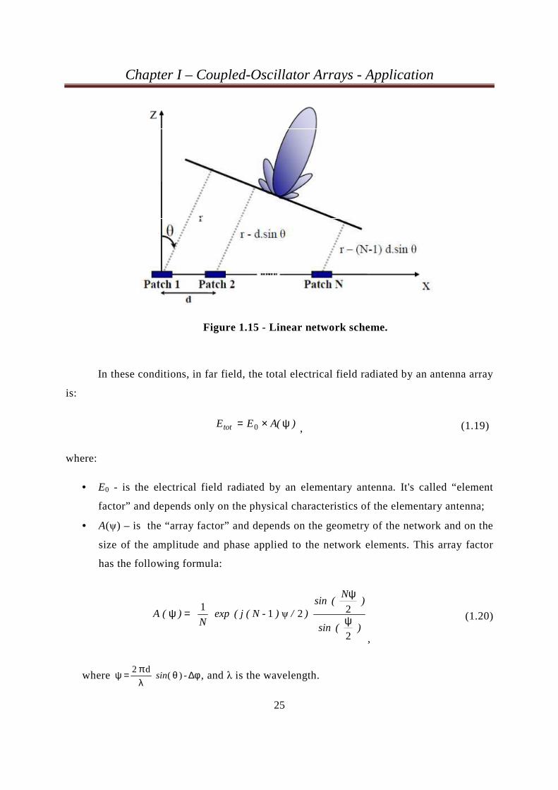
Figure 1.15 - Linear network scheme.
In these conditions, in far field, the total electrical field radiated by an antenna array
is:
)(AEEtot ψ×= 0 , (1.19)
where:
• E0 - is the electrical field radiated by an elementary antenna. It's called “element
factor” and depends only on the physical characteristics of the elementary antenna;
• A(ψ) – is the “array factor” and depends on the geometry of the network and on the
size of the amplitude and phase applied to the network elements. This array factor
has the following formula:
) ( sin
)N
( sin) / ) ( j ( N -exp
N )A (
2
2 2 ψ11
ψ
ψ
=ψ
,
(1.20)
where φ∆θλπ=ψ -) (
d 2 sin , and λ is the wavelength.
Chapter I – Coupled-Oscillator Arrays - Application
26
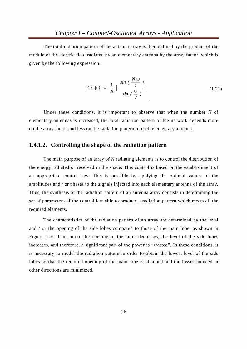
The total radiation pattern of the antenna array is then defined by the product of the
module of the electric field radiated by an elementary antenna by the array factor, which is
given by the following expression:
) ( sin
)N
( sin
N )A (
2
2
1
ψ
ψ
=ψ
.
(1.21)
Under these conditions, it is important to observe that when the number N of
elementary antennas is increased, the total radiation pattern of the network depends more
on the array factor and less on the radiation pattern of each elementary antenna.
1.4.1.2. Controlling the shape of the radiation pattern
The main purpose of an array of N radiating elements is to control the distribution of
the energy radiated or received in the space. This control is based on the establishment of
an appropriate control law. This is possible by applying the optimal values of the
amplitudes and / or phases to the signals injected into each elementary antenna of the array.
Thus, the synthesis of the radiation pattern of an antenna array consists in determining the
set of parameters of the control law able to produce a radiation pattern which meets all the
required elements.
The characteristics of the radiation pattern of an array are determined by the level
and / or the opening of the side lobes compared to those of the main lobe, as shown in
Figure 1.16. Thus, more the opening of the latter decreases, the level of the side lobes
increases, and therefore, a significant part of the power is “wasted”. In these conditions, it
is necessary to model the radiation pattern in order to obtain the lowest level of the side
lobes so that the required opening of the main lobe is obtained and the losses induced in
other directions are minimized.
Chapter I – Coupled-Oscillator Arrays - Application
27
Figure 1.16 – The imposed sizes of the level and opening for the main and side
lobes.
Due to these considerations, three synthesis solutions can be envisaged. The first is
to synthesize only the amplitude. This technique yields the direction lobes with the
possibility of controlling the level of the side lobes. The coefficients of the array can be
calculated using analytical techniques developed among others by Fourier or Chebyshev.
However, applications of this type of synthesis are limited. Thus, this solution is not
studied in detail in this manuscript. The other two solutions are presented in the following.
1.4.1.2.1. Phase synthesis
This solution allows to perform beam-steering of the antenna array. To do so,
several solutions with phase shifters or phase shifterless can be used as described below:
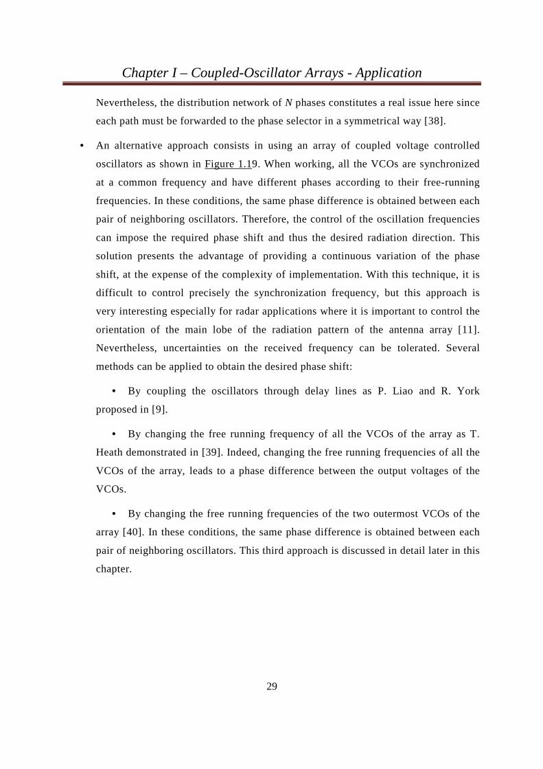
• A first approach illustrated in Figure 1.17 is relatively well known. The intermediate
frequency IF of the signal is converted in a RF frequency thanks to the oscillator
LO. The resulting signal is then divided using power dividers. Each of the obtained
signals is then amplified and phase shifted before being sent to the antenna elements
of the array. The concept of this approach is simple, but these devices can introduce
significant losses and a significant production cost. Moreover, the phase shifters are
Chapter I – Coupled-Oscillator Arrays - Application
28
passive devices difficult to integrate, and therefore their use in hybrid circuits is
limited.
• Furthermore, in the area of passive beam distributors, two classes coexist [33]:
1- The quasi-optical types: they imply a hybrid arrangement meaning either a
reflector or a lens objective with an antenna array. The quasi-optical type which
is the best known is the Rotman lens [34] which is a time delay device having
the synthesis procedure based on the optical geometry principles. The input or
output ports drive the cavity of a lens whose periphery is well defined. The
excitation of an input port produces a uniform amplitude distribution and a linear
phase gradient (constant) at the output ports. The Rotman lens is interesting
because it allows a certain freedom of design with many parameters to adjust,
one can obtain many beams with a stable frequency system. However, its
disadvantages are not negligible, especially regarding the complexity of the
design due to the number of variables to adjust and the mutual coupling between
its ports.
2- The circuits’ types using the microstrip technology, striplines or waveguides
such as the Butler matrix [35] which is a symmetrical passive mutual circuit with
N input ports and N output ports. This circuit drives N radiating elements
producing N different orthogonal beams. This is a parallel system made of
junctions which connect the input ports to the output ports through equal length
transmission lines. Thus, an input signal is many times divided without losses
until the output ports. Despite its simple and lossless architecture, the Butler
matrix has many disadvantages particularly regarding the number of components
which increases considerably with the number of desired beams.
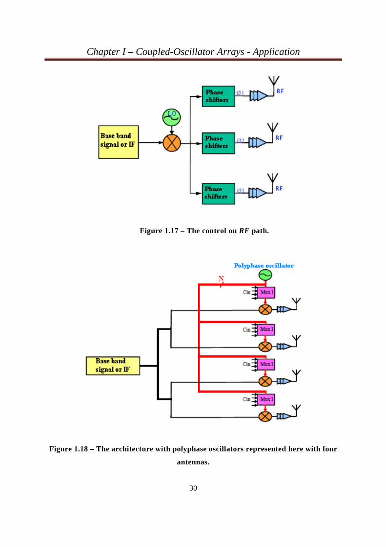
• Another approach illustrated in Figure 1.18, consists in using a polyphase voltage-
controlled oscillator, which is able to generate the local oscillator frequency with N
phases. In this architecture, all the N phases are conveyed to each antenna via a
distribution network. Phase selectors ensure the required phase to each element [36,
37]. In this case, the phase variations are discrete, which does not constitute a
problem as long as the discrimination steps are adequate to the application.
Chapter I – Coupled-Oscillator Arrays - Application
29
Nevertheless, the distribution network of N phases constitutes a real issue here since
each path must be forwarded to the phase selector in a symmetrical way [38].
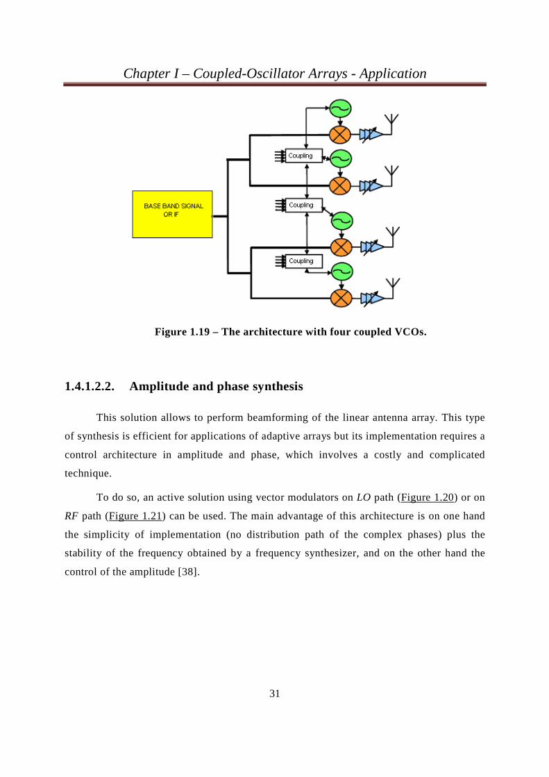
• An alternative approach consists in using an array of coupled voltage controlled
oscillators as shown in Figure 1.19. When working, all the VCOs are synchronized
at a common frequency and have different phases according to their free-running
frequencies. In these conditions, the same phase difference is obtained between each
pair of neighboring oscillators. Therefore, the control of the oscillation frequencies
can impose the required phase shift and thus the desired radiation direction. This
solution presents the advantage of providing a continuous variation of the phase
shift, at the expense of the complexity of implementation. With this technique, it is
difficult to control precisely the synchronization frequency, but this approach is
very interesting especially for radar applications where it is important to control the
orientation of the main lobe of the radiation pattern of the antenna array [11].
Nevertheless, uncertainties on the received frequency can be tolerated. Several
methods can be applied to obtain the desired phase shift:
• By coupling the oscillators through delay lines as P. Liao and R. York
proposed in [9].
• By changing the free running frequency of all the VCOs of the array as T.
Heath demonstrated in [39]. Indeed, changing the free running frequencies of all the
VCOs of the array, leads to a phase difference between the output voltages of the
VCOs.
• By changing the free running frequencies of the two outermost VCOs of the
array [40]. In these conditions, the same phase difference is obtained between each
pair of neighboring oscillators. This third approach is discussed in detail later in this
chapter.
Chapter I – Coupled-Oscillator Arrays - Application
30
Figure 1.17 – The control on RF path.
Figure 1.18 – The architecture with polyphase oscillators represented here with four
antennas.
Chapter I – Coupled-Oscillator Arrays - Application
31
Figure 1.19 – The architecture with four coupled VCOs.
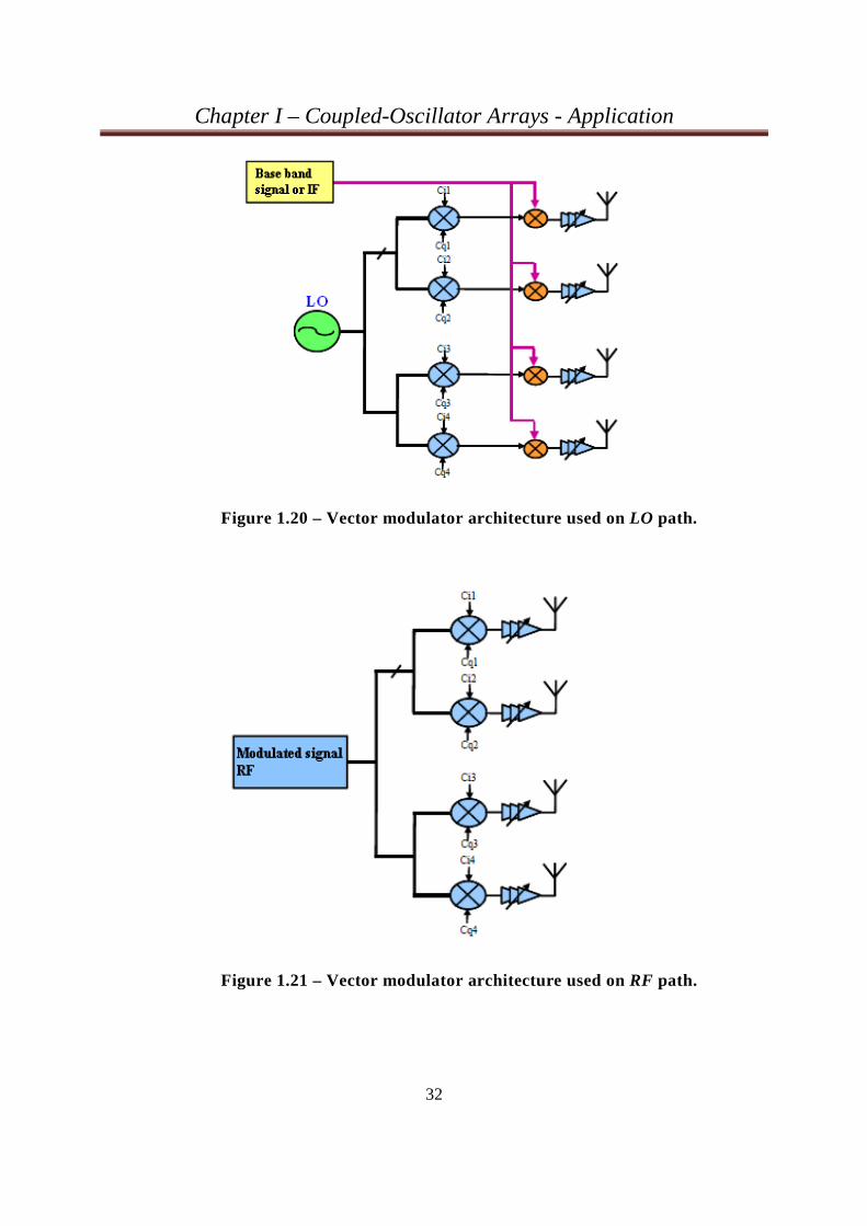
1.4.1.2.2. Amplitude and phase synthesis
This solution allows to perform beamforming of the linear antenna array. This type
of synthesis is efficient for applications of adaptive arrays but its implementation requires a
control architecture in amplitude and phase, which involves a costly and complicated
technique.
To do so, an active solution using vector modulators on LO path (Figure 1.20) or on
RF path (Figure 1.21) can be used. The main advantage of this architecture is on one hand
the simplicity of implementation (no distribution path of the complex phases) plus the
stability of the frequency obtained by a frequency synthesizer, and on the other hand the
control of the amplitude [38].
Chapter I – Coupled-Oscillator Arrays - Application
32
Figure 1.20 – Vector modulator architecture used on LO path.
Figure 1.21 – Vector modulator architecture used on RF path.
Chapter I – Coupled-Oscillator Arrays - Application
33
1.4.2. The control of the radiation pattern using coupled oscillators
As mentioned in subsection 1.4.1.2.1, R. York & al. introduced a new approach
based on using the synchronization propriety of coupled oscillators to steer the radiation
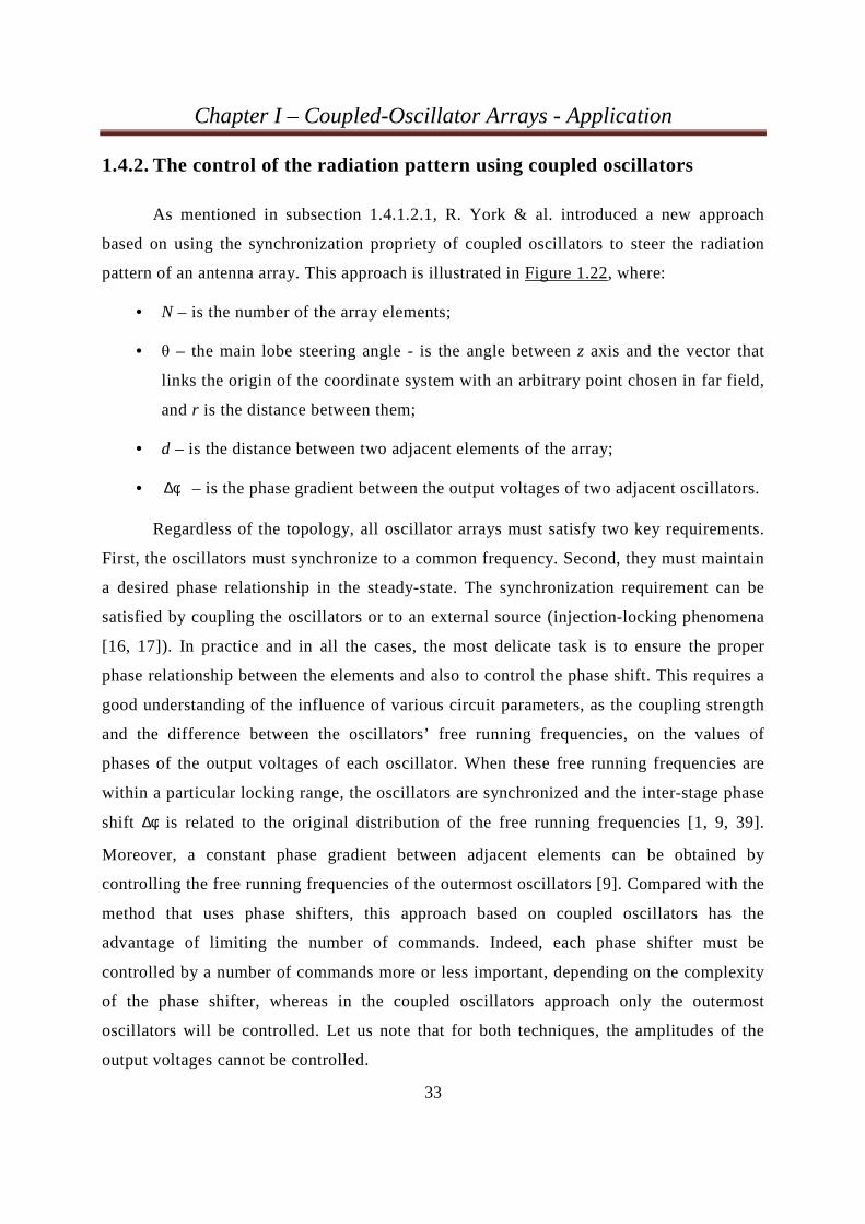
pattern of an antenna array. This approach is illustrated in Figure 1.22, where:
• N – is the number of the array elements;
• θ – the main lobe steering angle - is the angle between z axis and the vector that
links the origin of the coordinate system with an arbitrary point chosen in far field,
and r is the distance between them;
• d – is the distance between two adjacent elements of the array;
• φ∆ – is the phase gradient between the output voltages of two adjacent oscillators.
Regardless of the topology, all oscillator arrays must satisfy two key requirements.
First, the oscillators must synchronize to a common frequency. Second, they must maintain
a desired phase relationship in the steady-state. The synchronization requirement can be
satisfied by coupling the oscillators or to an external source (injection-locking phenomena
[16, 17]). In practice and in all the cases, the most delicate task is to ensure the proper
phase relationship between the elements and also to control the phase shift. This requires a
good understanding of the influence of various circuit parameters, as the coupling strength
and the difference between the oscillators’ free running frequencies, on the values of
phases of the output voltages of each oscillator. When these free running frequencies are
within a particular locking range, the oscillators are synchronized and the inter-stage phase
shift φ∆ is related to the original distribution of the free running frequencies [1, 9, 39].
Moreover, a constant phase gradient between adjacent elements can be obtained by
controlling the free running frequencies of the outermost oscillators [9]. Compared with the
method that uses phase shifters, this approach based on coupled oscillators has the
advantage of limiting the number of commands. Indeed, each phase shifter must be
controlled by a number of commands more or less important, depending on the complexity
of the phase shifter, whereas in the coupled oscillators approach only the outermost
oscillators will be controlled. Let us note that for both techniques, the amplitudes of the
output voltages cannot be controlled.
Chapter I – Coupled-Oscillator Arrays - Application
34
Figure 1.22 – Block diagram of an antenna array using coupled oscillators.
Nevertheless, it is shown in [1] that the theoretical limit of the phase shift that can
be obtained by slightly detuning the oscillators of the array by equal amounts but in
opposite directions is only ±90o. Therefore, it seems to be interesting to analyze the
behavior of an array of coupled differential VCOs since, in this case the theoretical limit of
the phase shift is within 360o due to the differential nature of the array. In these conditions,
a continuously controlled 360o phase shifting range can be obtained leading to a more
efficient beam-scanning architecture. Furthermore, differential oscillators or VCOs are
widely used in high-frequency circuit design due to their relatively good phase noise
performances and ease of integration. In this context, R. York’s theory is used to analyze
the behavior of an array of coupled differential VCOs. This theoretical study has then been
used to develop a CAD tool, allowing to obtain, in a very short simulation time, the
graphical representation of the locked states of the coupled differential oscillators. Thus,
from this cartography it will be possible to extract the values of the free running
frequencies required to generate the desired phase shift. The results obtained with the CAD
tool will then be compared with simulations using Agilent’s ADS software.
Chapter I – Coupled-Oscillator Arrays - Application
35
1.5. CONCLUSION
In this chapter a review of coupled-oscillator arrays as well as their applications was
presented. Thus, after a classification of oscillators in accordance with the waveform they
produce and the circuitry required for producing the desired oscillations.
A state of the art of coupled-oscillators theory was presented followed by a few
applications of antenna arrays. Due to their different geometric configuration, antenna
arrays can have an important role in controlling the radiation angle of the pattern.
Therefore, and also for simplicity reasons, a linear configuration was presented in this
chapter. Controlling the antenna array consists in generating the amplitudes and/or the
phases necessary for orientating the radiation pattern in the desired direction. As a
consequence, various technical solutions were proposed, including the coupled oscillators
approach.
36
CHAPTER II
Theoretical Analysis of Coupled Oscillators Applied
to an Antenna Array
Chapter II– Theoretical Analysis of Coupled Oscillators Applied to an Antenna Array
37
2.1. INTRODUCTION
Arrays of coupled oscillators are the subject of increasing research activity in the
communications systems due to their use in new applications such as power-combining
techniques and beam steering of antenna arrays.
In this context, let us remind that, the theoretical limit of the phase shift obtained
for an array of single-ended coupled oscillators is within the range of ±90° [1]. Thus, it
seems interesting to analyze the behavior of an array of differential VCOs. Indeed, in
this case, the theoretical limit of the phase shift is within 360° due to the differential
nature of the array, leading to a more efficient beam-scanning architecture for instance.
Furthermore, differential oscillators are widely used in high-frequency circuit design
due to their relatively good phase noise performances and ease of integration.
Moreover, the use of a broadband coupling network, i.e. a resistor, instead of a resonant
one, can lead to a substantial save in chip area in the case of RF integrated circuit
design.
Due to these considerations, in this chapter we will first remind R. York’s theory
giving the dynamics for two Van der Pol oscillators coupled through a resonant
network. Then, the dynamics of two Van der Pol oscillators coupled through a
broadband circuit will be presented. A new formulation of the equations describing the
locked states of two coupled Van der Pol oscillators using an accurate model allowing a
good prediction of the amplitudes will be then described. Finally, mathematical
manipulations will be applied to the dynamic equations describing the locked states of
the coupled Van der Pol oscillators. A reduced system of equations with no
trigonometric aspects will be obtained, leading to the elaboration of a CAD tool that
provides, in a considerably short simulation time, the frequency locking region of two
differential oscillators coupled through a resistive network, in terms of the amplitudes
of their output signals and the phase shift between them.
Chapter II– Theoretical Analysis of Coupled Oscillators Applied to an Antenna Array
38
2.2. DYNAMICS OF TWO VAN DER POL OSCILLATORS
COUPLED THROUGH A RESONANT CIRCUIT
Let us remember that the primary objective of this work is to orientate the
radiation pattern of an antenna array by controlling the phase gradient existing between
the signals applied to adjacent elements of the array. Thus, this chapter considers the
case of a system of two oscillators coupled first through a RLC circuit which provides
the synchronization frequency [19]. Indeed, the radiation pattern of a phased antenna
array is steered in a particular direction through a constant phase progression in the
oscillator chain which is obtained by detuning the free running frequencies of the
outermost oscillators in the array. Furthermore, it is shown that the resulting inter-stage
phase shift is independent on the number of oscillators in the array [9].
First, the oscillators are modeled by two Van der Pol circuits. The choice of this
model is justified by its simplicity regarding the analytical calculations, as presented in
[1]. This model is made of a RLC resonator and a nonlinear conductance, which has the
following expression:
231 VaaGNL +−= , (2.1)
where:
• -a1 is the negative conductance necessary to start the oscillation;
• a3V 2 is the nonlinear conductance which modelizes the saturation phenomenon.
In Figure 2.1, this nonlinear conductance is represented by the term G(A), given
by the following expression:
)A(fG)A(G 0−= , (2.2)
where:
• G0 is the negative conductance for a null control voltage;
• )A()A(f 21−= is the saturation function of the nonlinear conductance.
Chapter II– Theoretical Analysis of Coupled Oscillators Applied to an Antenna Array
39
Figure 2.1 – Two Van der Pol oscillators coupled through a RLC circuit.
Therefore, each oscillator is modeled by the negative conductance G(A),
associated to a parallel resonant circuit. These two oscillators are coupled through a
series resonant circuit, as shown in Figure 2.1. Let us note that both oscillators have the
same characteristics, except for their free running frequencies.
The main objective is to determine the phase shift φ∆ between the output
voltages of both oscillators, depending on their free-running frequencies referred to the
resonant frequency of the coupling circuit, when the system is synchronized.
The coupling current Ic can be expressed in terms of the admittance of the
oscillator 1, Y1(A1, ω1), of the admittance of the oscillator 2, Y2(A2, ω2), or depending on
the admittance of the coupling circuit, Yc(ωc), so that:
11111111 V)](Y)A(G[V),A(YI Lc ω+=ω=
22222222 V)](Y)A(G[V),A(YI Lc ω+−=ω−=
)VV)((YI ccc 21 −ω−= ,
(2.3)
where A1, ω1 represents the amplitude and pulsation of oscillators 1, A2, ω2
represents the amplitude and pulsation of oscillators 2, and V1 and V2 are the output
voltages of oscillator 1 and oscillator 2 respectively.
The admittance of oscillator 1, Y1(A1,ω1), can be expressed as follows:
Chapter II– Theoretical Analysis of Coupled Oscillators Applied to an Antenna Array
40
)(j
C)A(fGCj
Lj)A(fG),A(Y 2
1201
1101
1110111
1 ω−ωω
+−=ω+ω
+−=ω , (2.4)
where CL1
011=ω is the resonance pulsation of the resonator of oscillator 1.
Now, if 011 ω≅ω then 1101 2ω≅ω+ω and if C
Ga
02 =ω is the frequency bandwidth
of the two oscillators, then Y1(A1,ω1) can be written as is equation (2.5):
ωω−ω
+−=ωa
j)A(fG),A(Y 10110111 . (2.5)
Similarly, the admittance of oscillator 2, Y2(A2,ω2), is calculated and expressed in
the following equation:
ωω−ω
+−=ωa
j)A(fG),A(Y 20220222 , (2.6)
where CL2
021=ω is the resonance pulsation of the resonator of oscillator 2.
Knowing the expressions (2.5) and (2.6) of the admittances, it is important to
determine the expression of the current through the coupling circuit. To do so, the
complex output voltages of oscillators 1 and 2, are expressed as in equation (2.7):
111
θ= jeAV
222
θ= jeAV ,
(2.7)
where 111 φ+ω=θ t and 222 φ+ω=θ t . In this expression, the amplitudes A1 and A2,
and the phases 1φ and 2φ , are considered constants. In the case of oscillators, the values
of the amplitudes and phases are slowly varying [41], so that:
Chapter II– Theoretical Analysis of Coupled Oscillators Applied to an Antenna Array
41
)t(j)t(j eA)jj(eAdt
Vd1111
11111 φ+ωφ+ω φ+ω+=
)t(j)t(j eA)jj(eAdt
Vd2222
22222 φ+ωφ+ω φ+ω+= .
(2.8)
Hence,
)t(j
.
e)A
Aj(jA
dt
Vd11
1
1111
1 φ+ω−φ+ω=
)t(j
.
e)A
Aj(jA
dt
Vd22ω
2
2222
2ω
φ+−φ+=
.
(2.9)
Comparing equation (2.9) with the result from Fourier theory, Kurokawa
concluded that the expression in the brackets must be the time-domain representation of
the instantaneous frequency [17]. Using this expression for the pulsation ω, so that
ω = ω1,2 + δω with δω=−φ
.
A
Aj
1
11
or δω=−φ
.
A
Aj
2
22
, allows (2.5) and (2.6) to be expanded
in a Taylor series about the pulsations ω1,2 in order to study the behavior around the
oscillation pulsation ω1,2. Thus, for δω ‹‹ ω1,2, we have:
1
1
11
11
11111
θ
ω
φ+ω
−φω
ω+ω= j
.
)t(jc eA)
A
Aj(
d
),A(dY),A(YeI cc
2
2
22
22
22222
θ
ω
φ+ω
−φω
ω+ω−= j
.
)t(jc eA)
A
Aj(
d
),A(dY),A(YeI cc
.
(2.10)
If we divide the expressions (2.10) by 1θje and respectively 2θje , and replace
the derivate of the admittance depending on the pulsation ω, we obtain:
Chapter II– Theoretical Analysis of Coupled Oscillators Applied to an Antenna Array
42
11
11
0101010
1 A)A
Aj(
GjjG)A(fGeI
.
aa
)(jc
c
−φω
+ω
ω−ω−−=θ−θ
22
22
0202020
2 A)A
Aj(
GjjG)A(fGeI
.
aa
)(jc
c
−φω
−ω
ω−ω+=θ−θ
.
(2.11)
By separating the real part from the imaginary part, we obtain the following
expressions:
acc
AGA)A(fG)cos(I
ω+−=θ−θ 10
1101
acc
AGA)A(fG)cos(I
ω−=θ−θ 20
2202
110101
101 φω
+ω
ω−ω−=θ−θ A
GAG)sin(I
aacc
220202
202 φω
−ω
ω−ω=θ−θ A
GAG)sin(I
aacc .
(2.12)
Thus, from the equations above we can deduce 1A , 2A , 1θ and 2θ , as follows:
)cos(G
IA)A(fA c
caa θ−θω+ω= 1
0111
)sin(AG
Ic
ca θ−θω
−ω=θ 110
011
)cos(G
IA)A(fA c
caa θ−θω−ω= 2
0222
(2.13)
Chapter II– Theoretical Analysis of Coupled Oscillators Applied to an Antenna Array
43
)sin(AG
Ic
ca θ−θω+ω=θ 220
022 .
In (2.13), the dynamic equations for the amplitude and the phase of two coupled
oscillators are expressed [42]. Therefore, the next step is to find the dynamic equations
for the amplitude and the phase of the coupling current, Ic. The admittance of the
coupling circuit, Yc has the following expression:
ωωω−ω
−
=
ω+ω+
=ω
acc
ccc
ccccc
cc
jR
CjLjR
)(Y
21
111
122
0
, (2.14)
where ccCLc
10 =ω is the resonance pulsation of the coupling circuit, and
c
cac L
R=ω2 is the bandwidth of the coupling circuit. If we suppose that the
synchronization frequency of the coupling circuit ωc is close to the resonance pulsation
of the coupling circuit ω0c, then (2.14) can be written as follows:
)(D
)(N
jR
)(Ycc
cc
ac
ccccc ω
ω=
ωω−ω
−
≅ω01
11
. (2.15)
Thus, the coupling current can be written as follows:
)](V)(V[)(D
)(N)](V)(V)[(Y)(I
c
ccc ω−ω×
ωω
=ω−ωω=ω 1212 , (2.16)
and
)](V)(V[)(N)(I)(D ccc ω−ω×ω=ω×ω 12 . (2.17)
By applying a Taylor series development about ωc, to Dc(ω), we obtain:
Chapter II– Theoretical Analysis of Coupled Oscillators Applied to an Antenna Array
44
( )1212
1 θθθ
ω−=
ω−ω
ω+ω jj
c
jcc
ccc eAeA
ReI)(
d
dD)(D c
c
. (2.18)
Hence,
( ) ( )[ ])sin(j)cos(A)sin(j)cos(AR
II
Ij
jj cccc
cc
c
cc
acac
cc θ−θ+θ−θ−θ−θ+θ−θ=
−φ
ω+
ωω−ω− 111222
0 11
.
(2.19)
By separating the real part from the imaginary part, we can deduce the dynamic
equations of the amplitude and the phase of the coupling current, so that:
[ ])cos(A)cos(AR
II ccc
accacc θ−θ−θ−θ
ω+ω−= 1122
[ ].
cccc
accc )sin(A)sin(A
IRθ−θ−θ−θω+ω=θ 11220
.
(2.20)
Let us remind that the purpose of this work is to steer the beam of an antenna
array in a required direction. This direction leads to a phase gradient that exists between
the signals applied to adjacent elements of the array. This phase gradient is controlled
by the free-running frequencies of the oscillators which are located at the extremes of
the array. However, an important condition must be satisfied in order to achieve this
scope: the oscillators of the array must be synchronized at a common frequency. Thus,
we will present here a system of equations which defines the synchronization states of
the oscillators, using the dynamic equations written above.
Let us first define the notations Acx and Acy, from the following expression of the
coupling current:
)sin(jI)cos(IeI ccccj
cc θ+θ=θ
. (2.21)
So that,
Chapter II– Theoretical Analysis of Coupled Oscillators Applied to an Antenna Array
45
)cos(G
IA c
ccx φ=
0
)sin(G
IA c
ccy φ=
0,
(2.22)
where
)t(t)t( cc φ+ω=θ , )t(t)t( 11 φ+ω=θ , )t(t)t( 22 φ+ω=θ . (2.23)
Thus, using the notations above, and for a Van der Pol oscillator so that
)A()A(f 21−= , the equations (2.13) can be written as follows:
[ ])sin(A)cos(AA)A(A cycxaa 111211 1 φ+φω+−ω=
[ ])cos(A)sin(AA cycx
a11
1011 φ−φ
ω−ω−ω=φ
[ ])sin(A)cos(AA)A(A cycxaa 222222 1 φ+φω−−ω=
[ ])cos(A)sin(AA cycx
a22
2022 φ−φ
ω+ω−ω=φ
)sin(G
I)cos(
G
IA cc
cc
ccx φφ−φ=
00
)cos(G
I)sin(
G
IA cc
cc
ccy φφ+φ=
00,
(2.24)
where ω−θ=φ 11 , ω−θ=φ 22
and ω−θ=φ cc .
Replacing cI and cφ from the equations (2.20), we obtain the following
expressions for cxA and cyA :
Chapter II– Theoretical Analysis of Coupled Oscillators Applied to an Antenna Array
46
[ ])cos(A)cos(AA)(AA accyccxaccx 112200 φ−φλω+ω−ω+ω−=
[ ])sin(A)sin(AA)(AA accxccyaccy 112200 φ−φλω+ω−ω−ω−= ,
(2.25)
with the coupling constant 0
01
GRc
=λ .
The system is synchronized if the variations in time of amplitudes and phases are
null. Thus, the synchronization states can be determined by canceling the equations
(2.24). Under these conditions, cxA = 0 and cyA = 0, leading to:
))cos(A)cos(A(A)(A accyccxac 112200 φ−φλω=ω−ω−ω
))sin(A)sin(A(A)(A accxccyac 112200 φ−φλω=ω−ω+ω ,
(2.26)
We can see that the equations above can be put in matrix form, and Cramer's law
allows finding the expressions for Acx and Acy as shown below:
)]sin(A)sin(A[)]cos(A)cos(A[Aac
ccx 1122
201122
20 φ−φελ+φ−φελ= ω
ω∆
)]cos(A)cos(A[)]sin(A)sin(A[Aac
ccy 1122
201122
20 φ−φελ−φ−φελ= ω
ω∆ ,
(2.27)
where 2
1
1
ωω∆
+
=ε
ac
c
is the coupling strength scale factor and )Yarctan( 1=φ∆
is difference between the synchronization pulsation and the resonance pulsation of the
coupling circuit.
Now setting the other derivatives equal zero, so that 01 =A , 01 =φ , 02 =A and
02 =φ , gives the algebraic equations describing the locked states that, after eliminating
the coupling variables Acx and Acy, can be written as:
Chapter II– Theoretical Analysis of Coupled Oscillators Applied to an Antenna Array
47
)cos(AA)A( Φ−φ∆ελ−=ελ−− 2012
0211
)sin(A
Aac
ac
a Φ−φ∆εωλ−=ω∆
ωω
ελ−−ω∆1
20
2001 1
)cos(AA)A( Φ+φ∆ελ−=ελ−− 1022
0221
)sin(A
Aac
ac
a Φ+φ∆εωλ=ω∆
ωω
ελ−−ω∆2
10
2002 1
,
(2.28)
where
ωω∆
=Φac
carctan is the coupling phase, and the parameters ω01 and ω02,
are used to express the free running frequencies of the oscillators, ω01 and ω02, and the
resonance pulsation of the coupling circuit ω0c , as shown below:
c00101 ω−ω=ω∆
c00202 ω−ω=ω∆ .
Thus, a solution to (2.28) indicates the existence of a frequency-locked state and
provides the user with the amplitudes A1 and A2 of the two oscillators as well as the
inter-stage phase shift φ∆ and the synchronization pulsation ω for a combination
( )0201 ω∆ω∆ , .
Furthermore, let us note that the ability of the oscillators to synchronize
increases with the coupling strength and is maximum when the coupling phase is 0° or
180°. This can be demonstrated by expressing the scale factor of the coupling strength
as depending of the coupling phase Φ: 21
1
)][tan(Φ+=ε . Thus, for Φ = 0° or Φ = 180°,
ε = 1, the scale factor of the coupling strength is maximum. However, for a coupling
phase Φ = ±90°, ε = 0 and the ability of the oscillators to synchronize is then minimal.
Therefore, we can note that the ability of the oscillators to synchronize depends
critically on the phase of the coupling and thus on the proximity between the
Chapter II– Theoretical Analysis of Coupled Oscillators Applied to an Antenna Array
48
synchronization frequency and the resonant frequency of the coupling circuit compared
to the bandwidth of the coupling circuit.
Nevertheless, to simplify the analysis, J. Lynch and R. York made use of cases of
practical interest according to the tunings of oscillators 1 and 2 [19]. Indeed, for equal
tunings, i.e. for 0201 ω∆=ω∆ , and using the second and fourth equations of (2.28), one
can show that the phase difference φ∆ equals zero and the oscillators will always lock
no matter how far away from the origin we tune with equal amplitudes ( 21 AA = ).
On the other hand, when the coupling circuit resonance ( ocω ) is located exactly
between the two oscillators free-running frequencies, i.e. for 0201 ω∆−=ω∆ , one can
show, again using the second and fourth equations of (2.28), that 0 =ω∆ c , which
implies 0 =Φ and 21 AA = . In these conditions, the frequency difference between the
two free-running frequencies of oscillators 1 and 2 can be expressed, by subtracting the
fourth and second equations, as follows:
( )φ∆ωλ=ω∆ sina00 2 , (2.29)
with 01020 ω−ω=ω∆ as mentioned previously.
Furthermore, in the same conditions, the amplitudes are equal and found from
(2.28), by combining the first and third equation, as follows:
. 2
111 2
0
00
2
ωλω∆
−−λ−=a
A (2.30)
2.3. DYNAMICS OF TWO VAN DER POL OSCILLATORS
COUPLED THROUGH A BROAD-BAND CIRCUIT
Let us remember that, R. York described in [19] the oscillators’ dynamic
equations, as well as those for the amplitude and phase of the coupling current. Then, by
setting the derivatives equal to zero, the algebraic equations describing the oscillators’

Chapter II– Theoretical Analysis of Coupled Oscillators Applied to an Antenna Array
49
frequency locked states, for two Van der Pol oscillators coupled through a RLC circuit,
were obtained as detailed in the previous section. This system of four equations with
four unknowns is reminded as follows:
)cos(AA)A( Φ−φ∆ελ−=ελ−− 2012
0211
)sin(A
Aac
ac
a Φ−φ∆εωλ−=ω∆
ωω
ελ−−ω∆1
20
2001 1
)cos(AA)A( Φ+φ∆ελ−=ελ−− 1022
0221
)sin(A
Aac
ac
a Φ+φ∆εωλ=ω∆
ωω
ελ−−ω∆2
10
2002 1
,
The ability of these coupled oscillators to synchronize to a common frequency is
affected by the following parameters [10]:
• 2
1
1
ωω∆
+
=ε
ac
c
: coupling strength scale factor;
•
ωω∆=Φ −
ac
ctan 1 : coupling phase;
• cRG0
01=λ : coupling constant, where 0G is the first-order term of Van der Pol
nonlinear conductance;
• C
Ga
02 =ω : the oscillators’ bandwidth;
• c
cac L
R=ω2 : bandwidth of the unloaded coupling circuit;
• ω01, ω02 : free-running frequencies or tunings of oscillators 1 and 2,
respectively;
• ω0c : resonant frequency of the coupling circuit;
Chapter II– Theoretical Analysis of Coupled Oscillators Applied to an Antenna Array
50
• c00101 ω−ω=ω∆ c00202 ω−ω=ω∆ cc 0ω−ω=ω∆ .
In these conditions, the Broad-band case is found by letting the coupling circuit
bandwidth approach infinity so that ωac →∞, which means that the coupling circuit is
made of one resistor for instance [18]. Thus, if ωac →∞, this implies ε = 1 and Φ = 0. In
these conditions, the new equations describing the locked states can be written as:
)cos(AA)A( φ∆λ−=λ−− 2010211
)sin(A
Aac φ∆ωλ−=ω∆−ω∆
1
2001
)cos(AA)A( φ∆λ−=λ−− 1020221
)sin(A
Aac φ∆ωλ=ω∆−ω∆
2
1002
.
(2.31)
Since ω−ω=ω∆−ω∆ 0101 c and ω−ω=ω∆−ω∆ 0202 c ,
Thus, we have:
)cos(AA)A( φ∆λ−=λ−− 2010211
)sin(A
Aa φ∆ωλ−ω=ω
1
2001
)cos(AA)A( φ∆λ−=λ−− 1020221
)sin(A
Aa φ∆ωλ+ω=ω
2
1002
.
(2.32)
Chapter II– Theoretical Analysis of Coupled Oscillators Applied to an Antenna Array
51
2.4. NEW FORMULATION OF THE EQUATIONS DESCRIBING
THE LOCKED STATES OF TWO VAN DER POL COUPLED
OSCILLATORS ALLOWING A MORE ACCURATE
PREDICTION OF THE AMPLITUDES
2.4.1. Two Van der Pol oscillators coupled through a resonant network
The purpose of this section is to propose a new formulation of the equations
describing the locked states of two Van der Pol oscillators coupled through a resonant
network using an accurate model allowing a good prediction of the oscillators’
amplitudes.
Indeed, let us remember that the Van der Pol model used by R. York in [19] is
described by the following equation:
200 AGG)A(G +−= ,
(2.33)
where G0 is the device conductance at zero voltage.
Nevertheless, the free-running amplitude of such a Van der Pol oscillator is
shown to be equal to 1 irrespective of the value of G0. As a consequence, this model
doesn’t allow an accurate prediction of the amplitudes of the two coupled oscillators.
To illustrate this affirmation, let us explain the assumptions and approximations
made by J. Lynch and R. York in [19] for the modelling of a Van der Pol oscillator.
Indeed, let us first consider the schematic of a Van der Pol oscillator as shown in Figure
2.2 for which the current in the nonlinear conductance GNL is equal to ( ) ( ) ( )tbvtavti 31 +−=
with –a the negative conductance necessary to start the oscillations and b a parameter
used to model the saturation phenomenon. In this case, according to the Kirchhoff's
current law, the current i(t) can be written as:
)t(v.b)t(v.Ga)t(i 3 )( ++−= . (2.34)
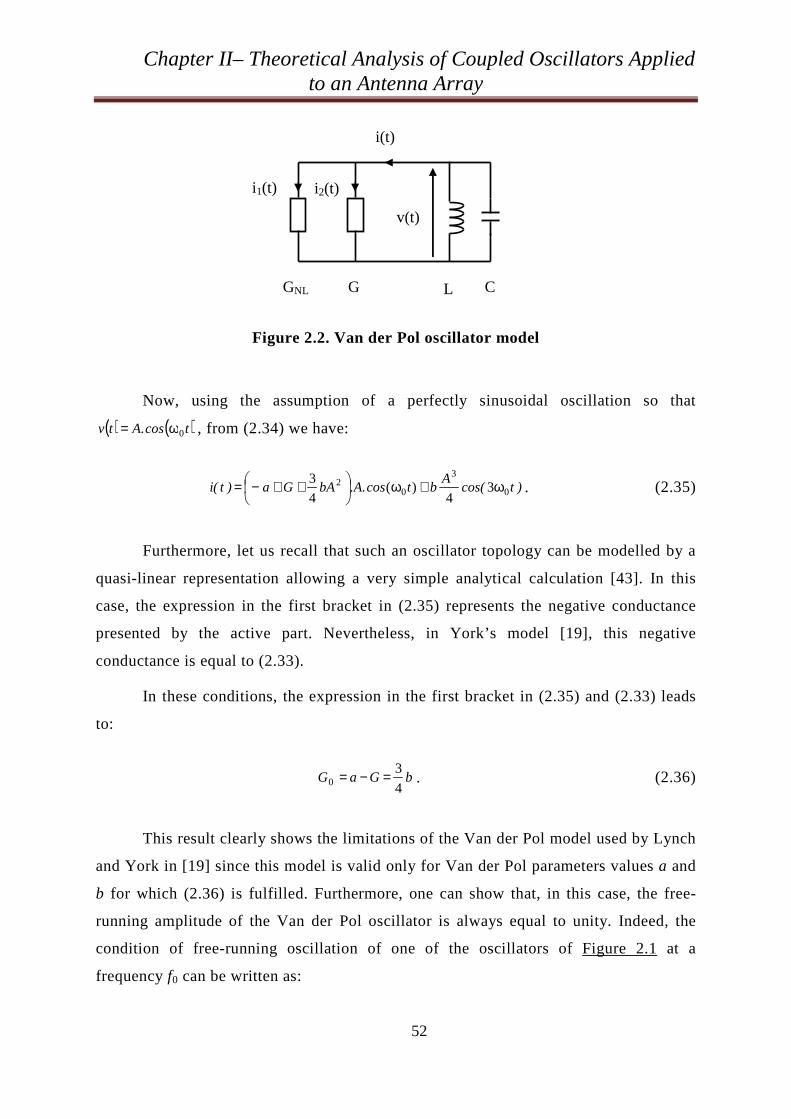
Chapter II– Theoretical Analysis of Coupled Oscillators Applied to an Antenna Array
52
Figure 2.2. Van der Pol oscillator model
Now, using the assumption of a perfectly sinusoidal oscillation so that
( ) ( )tcos.Atv 0 ω= , from (2.34) we have:
)tcos(A
btcos.A.bAGa)t(i 0
3
02 3
4 )(
4
3 ω+ω
++−= . (2.35)
Furthermore, let us recall that such an oscillator topology can be modelled by a
quasi-linear representation allowing a very simple analytical calculation [43]. In this
case, the expression in the first bracket in (2.35) represents the negative conductance
presented by the active part. Nevertheless, in York’s model [19], this negative
conductance is equal to (2.33).
In these conditions, the expression in the first bracket in (2.35) and (2.33) leads
to:
bGaG4
3 0 =−= . (2.36)
This result clearly shows the limitations of the Van der Pol model used by Lynch
and York in [19] since this model is valid only for Van der Pol parameters values a and
b for which (2.36) is fulfilled. Furthermore, one can show that, in this case, the free-
running amplitude of the Van der Pol oscillator is always equal to unity. Indeed, the
condition of free-running oscillation of one of the oscillators of Figure 2.1 at a
frequency f0 can be written as:
G
v(t)
GNL L C
i(t)
i1(t) i2(t)
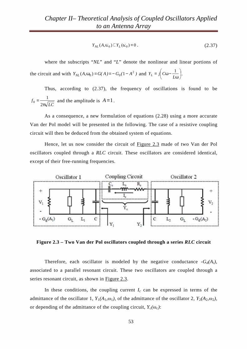
Chapter II– Theoretical Analysis of Coupled Oscillators Applied to an Antenna Array
53
0 )( )( 00 =ω+ω LNL Y,AY . (2.37)
where the subscripts “NL” and “L” denote the nonlinear and linear portions of
the circuit and with )A(G)A(G,AYNL2
00 1 )( −−==ω and
ω−ω=
LCjYL
1 .
Thus, according to (2.37), the frequency of oscillations is found to be
LCf
π=
2
10 and the amplitude is 1 =A .
As a consequence, a new formulation of equations (2.28) using a more accurate
Van der Pol model will be presented in the following. The case of a resistive coupling
circuit will then be deduced from the obtained system of equations.
Hence, let us now consider the circuit of Figure 2.3 made of two Van der Pol
oscillators coupled through a RLC circuit. These oscillators are considered identical,
except of their free-running frequencies.
Figure 2.3 – Two Van der Pol oscillators coupled through a series RLC circuit
Therefore, each oscillator is modeled by the negative conductance -Gd(Ai),
associated to a parallel resonant circuit. These two oscillators are coupled through a
series resonant circuit, as shown in Figure 2.3.
In these conditions, the coupling current Ic can be expressed in terms of the
admittance of the oscillator 1, Y1(A1,ω1), of the admittance of the oscillator 2, Y2(A2,ω2),
or depending of the admittance of the coupling circuit, Yc(ωc):
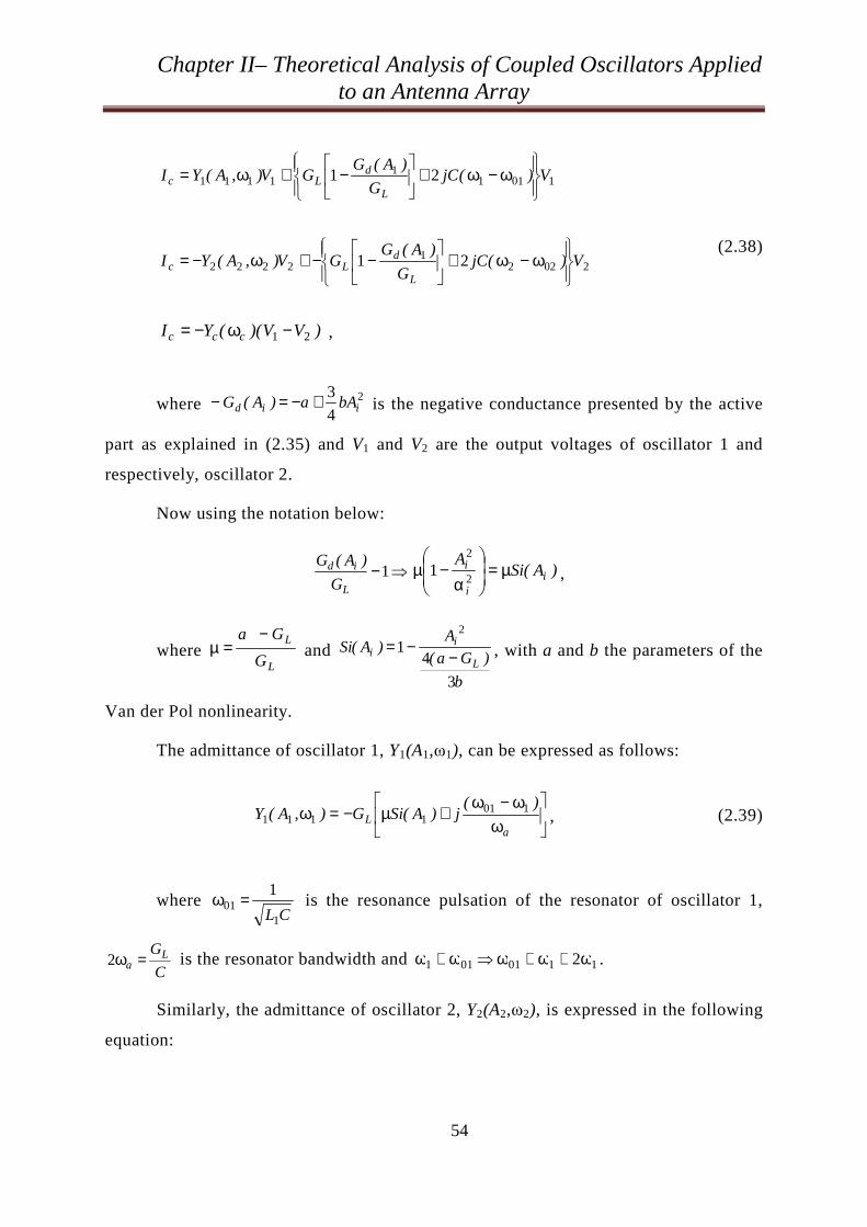
Chapter II– Theoretical Analysis of Coupled Oscillators Applied to an Antenna Array
54
10111
1111 21 V)(jCG
)A(GGV),A(YI
L
dLc
ω−ω+
−≅ω=
20221
2222 21 V)(jCG
)A(GGV),A(YI
L
dLc
ω−ω+
−−≅ω−=
)VV)((YI ccc 21 −ω−= ,
(2.38)
where 2
4
3iid bAa)A(G +−=− is the negative conductance presented by the active
part as explained in (2.35) and V1 and V2 are the output voltages of oscillator 1 and
respectively, oscillator 2.
Now using the notation below:
⇒−1L
id
G
)A(G)A(Si
Ai
i
i µ=
α−µ
2
2
1 ,
where L
L
G
Ga −=µ and
b
)Ga(
A)A(Si
L
ii
3
41
2
−−= , with a and b the parameters of the
Van der Pol nonlinearity.
The admittance of oscillator 1, Y1(A1,ω1), can be expressed as follows:
ωω−ω
+µ−=ωa
L)(
j)A(SiG),A(Y 1011111 , (2.39)
where CL1
011=ω is the resonance pulsation of the resonator of oscillator 1,
C
GLa =ω2 is the resonator bandwidth and 1101011 2ω≅ω+ω⇒ω≅ω .
Similarly, the admittance of oscillator 2, Y2(A2,ω2), is expressed in the following
equation:
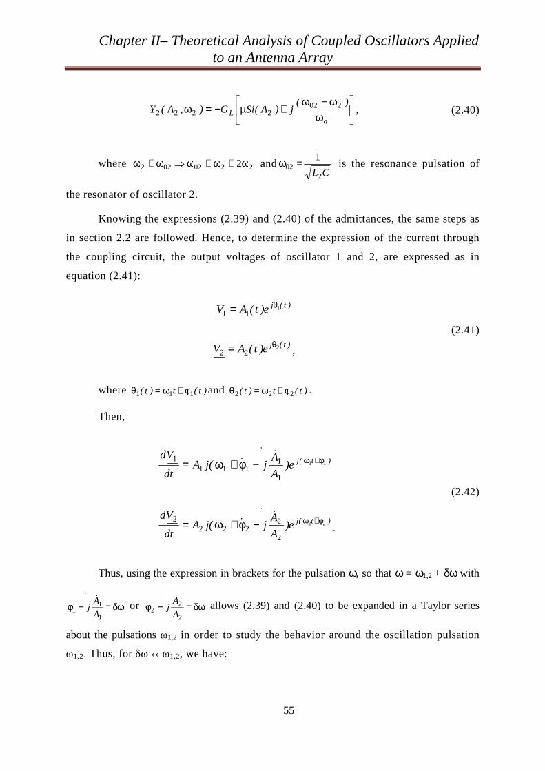
Chapter II– Theoretical Analysis of Coupled Oscillators Applied to an Antenna Array
55
ωω−ω
+µ−=ωa
L)(
j)A(SiG),A(Y 2022222 , (2.40)
where 2202022 2ω≅ω+ω⇒ω≅ω andCL2
021=ω is the resonance pulsation of
the resonator of oscillator 2.
Knowing the expressions (2.39) and (2.40) of the admittances, the same steps as
in section 2.2 are followed. Hence, to determine the expression of the current through
the coupling circuit, the output voltages of oscillator 1 and 2, are expressed as in
equation (2.41):
)t(je)t(AV 111
θ=
)t(je)t(AV 222
θ= ,
(2.41)
where )t(t)t( 111 φ+ω=θ and )t(t)t( 222 φ+ω=θ .
Then,
)t(j
.
e)A
Aj(jA
dt
Vd11
1
1111
1 φ+ω−φ+ω=
)t(j
.
e)A
Aj(jA
dt
Vd22
2
2222
2 φ+ω−φ+ω=
.
(2.42)
Thus, using the expression in brackets for the pulsation ω, so that ω = ω1,2 + δω with
δω=−φ
.
A
Aj
1
11
or δω=−φ
.
A
Aj
2
22
allows (2.39) and (2.40) to be expanded in a Taylor series
about the pulsations ω1,2 in order to study the behavior around the oscillation pulsation
ω1,2. Thus, for δω ‹‹ ω1,2, we have:
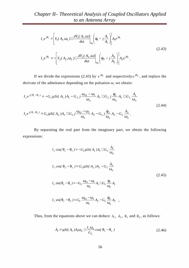
Chapter II– Theoretical Analysis of Coupled Oscillators Applied to an Antenna Array
56
1
1
11
11
11111
θ
ω
θ
−φ
ωω
+ω= jjc eA
A
Aj
d
),A(dY),A(YeI c
2
2
22
22
22222
θ
ω
θ
−φ
ωω
+ω−= jjc eA
A
Aj
d
),A(dY),A(YeI c
.
(2.43)
If we divide the expressions (2.43) by 1θje and respectively 2θje , and replace the
derivate of the admittance depending on the pulsation ω, we obtain:
aL
aL
aLL
)(jc
AGAjGAjGA)A(SiGeI c
ω+
ωφ+
ωω−ω
−µ−=θ−θ 11
11
10111
1
aL
aL
aLL
)(jc
AGAjGAjGA)A(SiGeI c
ω−
ωφ−
ωω−ω
+µ=θ−θ 22
22
20222
2
.
(2.44)
By separating the real part from the imaginary part, we obtain the following
expressions:
aLLcc
AGA)A(SiG)cos(I
ω+µ−=θ−θ 1
111
aLLcc
AGA)A(SiG)cos(I
ω−µ=θ−θ 2
222
11
1101
1 AGAG)sin(Ia
La
Lcc ωφ+
ωω−ω
−=θ−θ
22
2202
2 AGAG)sin(Ia
La
Lcc ωφ−
ωω−ω
=θ−θ
,
(2.45)
Thus, from the equations above we can deduce 1A , 2A , 1θ and 2θ , as follows:
)cos(G
IA)A(SiA c
L
aca θ−θω+ωµ= 1111
(2.46)
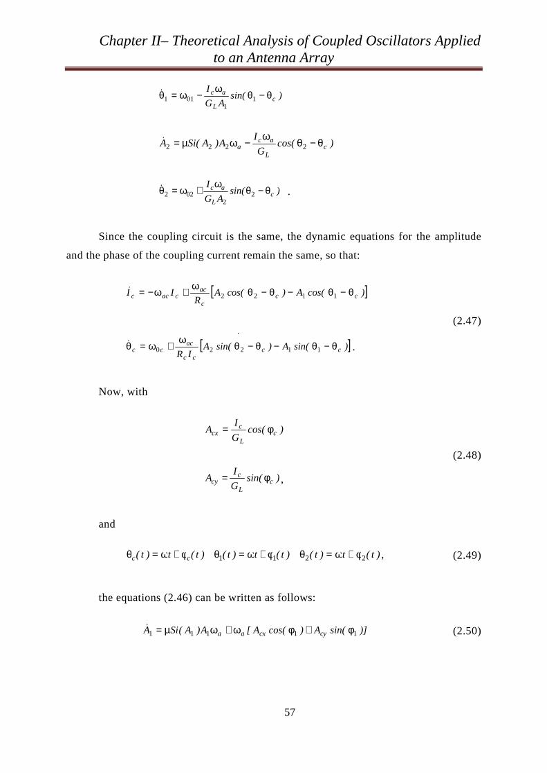
Chapter II– Theoretical Analysis of Coupled Oscillators Applied to an Antenna Array
57
)sin(AG
Ic
L
ac θ−θω
−ω=θ 11
011
)cos(G
IA)A(SiA c
L
aca θ−θω−ωµ= 2222
)sin(AG
Ic
L
ac θ−θω
+ω=θ 22
022
.
Since the coupling circuit is the same, the dynamic equations for the amplitude
and the phase of the coupling current remain the same, so that:
[ ])cos(A)cos(AR
II ccc
accacc θ−θ−θ−θω+ω−= 1122
[ ].
cccc
accc )sin(A)sin(A
IRθ−θ−θ−θ
ω+ω=θ 11220
.
(2.47)
Now, with
)cos(G
IA c
L
ccx φ=
)sin(G
IA c
L
ccy φ= ,
(2.48)
and
)t(t)t( cc φ+ω=θ )t(t)t( 11 φ+ω=θ )t(t)t( 22 φ+ω=θ , (2.49)
the equations (2.46) can be written as follows:
)]sin(A)cos(A[A)A(SiA cycxaa 11111 φ+φω+ωµ=
(2.50)
Chapter II– Theoretical Analysis of Coupled Oscillators Applied to an Antenna Array
58
)]cos(A)sin(A[A cycx
a11
1011 φ−φ
ω−ω−ω=φ
)]sin(A)cos(A[A)A(SiA cycxaa 22222 φ+φω−ωµ=
)]cos(A)sin(A[A cycx
a22
2022 φ−φ
ω+ω−ω=φ
)sin(G
I)cos(
G
IA cc
L
cc
L
ccx φφ−φ=
)cos(G
I)sin(
G
IA cc
L
cc
L
ccy φφ+φ=
.
where ω−θ=φ 11 , ω−θ=φ 22
and ω−θ=φ cc .
Replacing cI and cφ from the equations (2.47), we obtain the following
expressions for cxA and cyA :
[ ])cos(A)cos(AA)(AA accyccxaccx 112200 φ−φλω+ω−ω+ω−=
[ ])sin(A)sin(AA)(AA accxccyaccy 112200 φ−φλω+ω−ω−ω−= ,
(2.51)
with the coupling constant LcGR
10 =λ .
The system is synchronized if the variations in time of the amplitudes and the
phases are null. Thus, the synchronization states can be determined by canceling the
equations (2.51). Under these conditions, cxA = 0 and cyA = 0, leading to:
))cos(A)cos(A(A)(A accyccxac 112200 φ−φλω=ω−ω−ω
))sin(A)sin(A(A)(A accxccyac 112200 φ−φλω=ω−ω+ω .
(2.52)
We can see that the equations above can be put in matrix form, and Cramer's law
allows finding the expressions for Acx and Acy as shown below:
Chapter II– Theoretical Analysis of Coupled Oscillators Applied to an Antenna Array
59
)]sin(A)sin(A[)]cos(A)cos(A[Aac
ccx 1122
201122
20 φ−φελ+φ−φελ= ω
ω∆
)]cos(A)cos(A[)]sin(A)sin(A[Aac
ccy 1122
201122
20 φ−φελ−φ−φελ= ω
ω∆ ,
(2.53)
where 2
1
1
ωω∆
+
=ε
ac
c
is the coupling strength scale factor and cc 0ω−ω=ω∆ is
difference between the synchronization pulsation and the resonance pulsation of the
coupling circuit.
Now setting the derivatives equal zero, so that01 =A , 01 =φ , 02 =A and 02 =φ ,
gives the algebraic equations describing the locked states that, after eliminating the
coupling variables Acx and Acy, can be written as:
)cos(AA])A(Si[ Φ−φ∆ελ−=ελ−µ 2012
01
)sin(A
Aac
ac
a Φ−φ∆εωλ−=ω∆
ωω
ελ−−ω∆1
20
2001 1
)cos(AA])A(Si[ Φ+φ∆ελ−=ελ−µ 1022
02
)sin(A
Aac
ac
a Φ+φ∆εωλ=ω∆
ωωελ−−ω∆
2
10
2002 1
,
(2.54)
where
ωω∆
=Φac
carctan is the coupling phase, and c00101 ω−ω=ω∆ ,
c00202 ω−ω=ω∆ .
Thus, for the specific case of 0201 ω∆−=ω∆ , for which the coupling circuit
resonance is located exactly between the two oscillators free-running, one can show,
using (2.54), that 00 =ω−ω=ω∆ cc , which implies 1=ε , 0=Φ and A1 = A2 = A. As a
Chapter II– Theoretical Analysis of Coupled Oscillators Applied to an Antenna Array
60
consequence, the frequency difference between the two free-running frequencies of
oscillators 1 and 2 can also be expressed using (2.29) but with LcGR
10 =λ and
C
GLa =ω2 .
Nevertheless, since A1=A2= A then, from the system of equations above, we can
obtain the following expression:
)cos()A(Si φ∆λ−=λ−µ 00 . (2.55)
Since L
L
G
Ga −=µ and
b
)Ga(A
)A(SiL
3
41
2
−−= , replacing in equation (2.55) these
values, the new expression for the amplitude of both oscillators is:
)])(cos([Gab
A L 113
40 −φ∆λ−−= .
(2.56)
One can notice that this expression is different from the one obtained in equation
(2.30) and allows the prediction of the amplitudes of the two coupled Van der Pol
oscillators for any values of parameters a and b of the Van der Pol non linearity under a
sinusoidal assumption.
2.4.2. Resistive coupling case
As already mentioned in section 2.3, the case of a resistive coupling circuit is
found by letting the coupling circuit bandwidth approach infinity so that ∞→ωac
leading to 1 =ε and 0 =Φ . In these conditions, the new equations describing the locked
states can be deduced from equations (2.54) as follows :
)cos(AA))A(S( i φ∆λ−=λ−µ 20101
)sin(A
Aa φ∆ωλ−ω=ω
1
2001
)cos(AA))A(S( i φ∆λ−=λ−µ 10202
)sin(A
Aa φ∆ωλ+ω=ω
2
1002 .
(2.57)
Chapter II– Theoretical Analysis of Coupled Oscillators Applied to an Antenna Array
61
2.5. NEW FORMULATION OF THE EQUATIONS DESCRIBING
THE LOCKED STATES OF TWO VAN DER POL COUPLED
OSCILLATORS ALLOWING AN EASIER NUMERICAL
SOLVING METHOD
Once more, a solution to (2.54) indicates the existence of a frequency-locked
state for the two van der Pol coupled oscillators. However, in this case, one can obtain
the oscillators’ amplitudes A1 and A2 for any values of parameters a and b of the Van
der Pol non linearity under the assumption of a sinusoidal behavior as well as the inter-
stage phase shift φ∆ and the synchronization pulsation ω for a combination ( 0201 ω∆ω∆ ,
).
Nevertheless, due to the trigonometric and non-linear aspect of (2.54), the
solutions of this system are very difficult or impossible to obtain. In these conditions,
mathematical manipulations are applied to the equations in order to obtain a new system
of three equations with three unknowns A1, A2 and ω, easier to solve [10]. These
equations will allow then to determine the phase shift φ∆ according to the pulsations
ω01 and ω02. First we will write the equations (2.54) in another form, as shown below:
20
12
01
A
A])A(Si[)cos(
ελελ−µ−=Φ−φ∆
1
20
2001 1
A
A)sin(
a
cac
a
εωλ
ω∆
ωωελ−−ω∆
−=Φ−φ∆
10
22
02
A
A])A(Si[)cos(
ελελ−µ−=Φ+φ∆
2
10
2002 1
A
A)sin(
a
cac
a
εωλ
ω∆
ωω
ελ−−ω∆=Φ+φ∆ ,
(2.58)
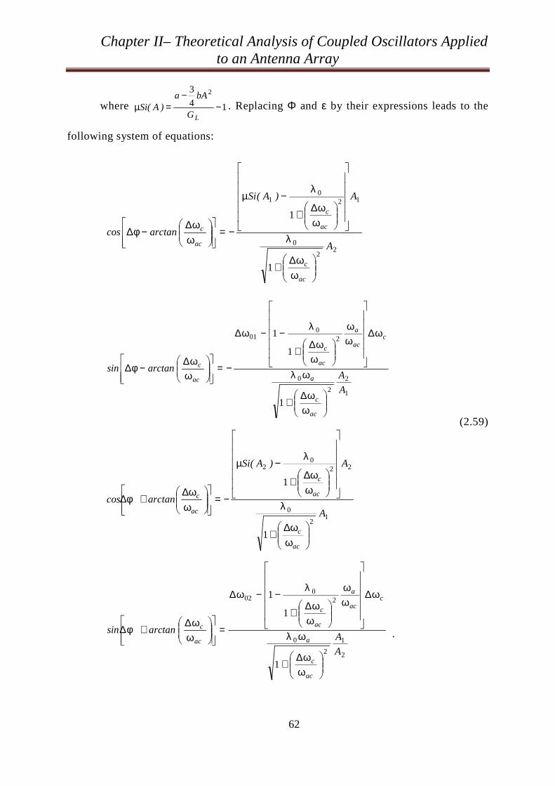
Chapter II– Theoretical Analysis of Coupled Oscillators Applied to an Antenna Array
62
where 14
3 2
−−
=µLG
bAa)A(Si . Replacing Φ and ε by their expressions leads to the
following system of equations:
22
0
120
1
1
1
A
A)A(Si
arctancos
ac
c
ac
c
ac
c
ωω∆
+
λ
ωω∆
+
λ−µ
−=
ωω∆
−φ∆
1
2
2
0
20
01
1
1
1
A
Aarctansin
ac
c
a
cac
a
ac
c
ac
c
ωω∆
+
ωλ
ω∆
ωω
ωω∆
+
λ−−ω∆
−=
ωω∆
−φ∆
12
0
220
2
1
1
A
A)A(Si
arctancos
ac
c
ac
c
ac
c
ωω∆
+
λ
ωω∆
+
λ−µ
−=
ωω∆
+φ∆
2
1
2
0
20
02
1
1
1
A
Aarctansin
ac
c
a
cac
a
ac
c
ac
c
ωω∆
+
ωλ
ω∆
ωω
ωω∆
+
λ−−ω∆
=
ωω∆
+φ∆ .
(2.59)
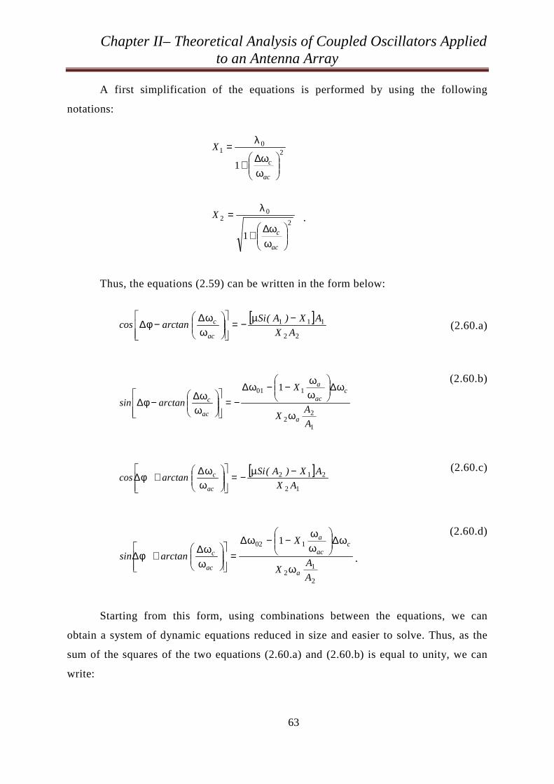
Chapter II– Theoretical Analysis of Coupled Oscillators Applied to an Antenna Array
63
A first simplification of the equations is performed by using the following
notations:
20
1
1
ωω∆
+
λ=
ac
c
X
2
02
1
ωω∆
+
λ=
ac
c
X .
Thus, the equations (2.59) can be written in the form below:
[ ]22
111
AX
AX)A(Siarctancos
ac
c −µ−=
ωω∆−φ∆ (2.60.a)
1
22
101 1
A
AX
X
arctansin
a
cac
a
ac
c
ω
ω∆
ωω
−−ω∆−=
ωω∆
−φ∆
(2.60.b)
[ ]12
212
AX
AX)A(Siarctancos
ac
c −µ−=
ωω∆+φ∆
(2.60.c)
2
12
102 1
A
AX
X
arctansin
a
cac
a
ac
c
ω
ω∆
ωω
−−ω∆=
ωω∆
+φ∆ .
(2.60.d)
Starting from this form, using combinations between the equations, we can
obtain a system of dynamic equations reduced in size and easier to solve. Thus, as the
sum of the squares of the two equations (2.60.a) and (2.60.b) is equal to unity, we can
write:
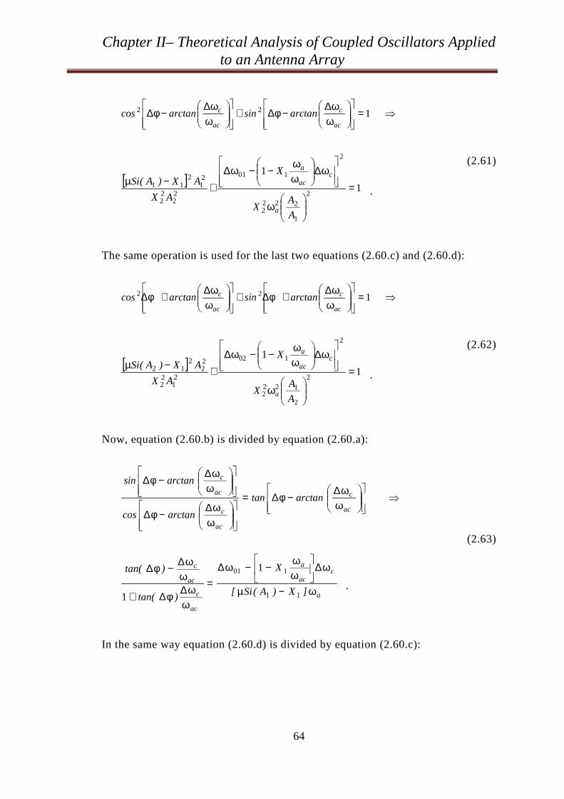
Chapter II– Theoretical Analysis of Coupled Oscillators Applied to an Antenna Array
64
⇒=
ωω∆
−φ∆+
ωω∆
−φ∆ 122
ac
c
ac
c arctansinarctancos
[ ]1
1
2
1
2222
2
101
22
22
21
211 =
ω
ω∆
ωω−−ω∆
+−µ
A
AX
X
AX
AX)A(Si
a
cac
a
.
(2.61)
The same operation is used for the last two equations (2.60.c) and (2.60.d):
⇒=
ωω∆
+φ∆+
ωω∆
+φ∆ 122
ac
c
ac
c arctansinarctancos
[ ]1
1
2
2
1222
2
102
21
22
22
212 =
ω
ω∆
ωω−−ω∆
+−µ
A
AX
X
AX
AX)A(Si
a
cac
a
.
(2.62)
Now, equation (2.60.b) is divided by equation (2.60.a):
⇒
ωω∆
−φ∆=
ωω∆
−φ∆
ωω∆
−φ∆
ac
c
ac
c
ac
c
arctantan
arctancos
arctansin
a
cac
a
ac
c
ac
c
]X)A(Si[
X
)tan(
)tan(
ω−µ
ω∆
ωω−−ω∆
=
ωω∆φ∆+
ωω∆−φ∆
11
101 1
1 .
(2.63)
In the same way equation (2.60.d) is divided by equation (2.60.c):
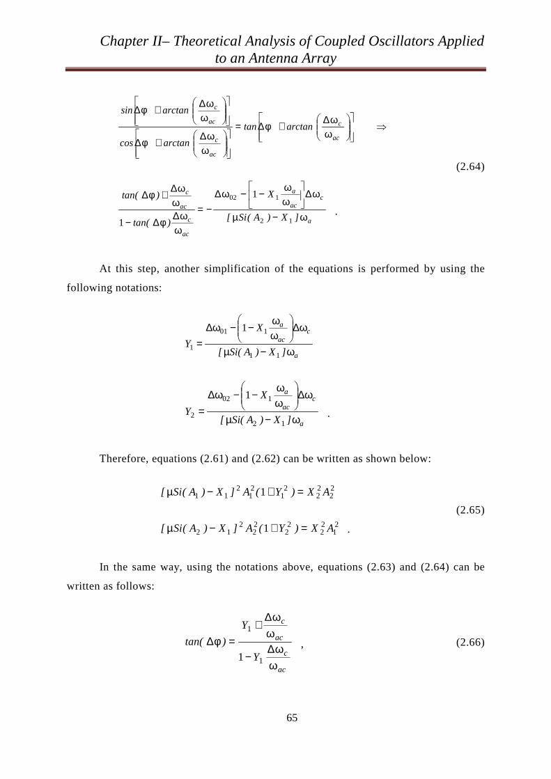
Chapter II– Theoretical Analysis of Coupled Oscillators Applied to an Antenna Array
65
⇒
ωω∆
+φ∆=
ωω∆
+φ∆
ωω∆+φ∆
ac
c
ac
c
ac
c
arctantan
arctancos
arctansin
a
cac
a
ac
c
ac
c
]X)A(Si[
X
)tan(
)tan(
ω−µ
ω∆
ωω−−ω∆
−=
ωω∆φ∆−
ωω∆+φ∆
12
102 1
1 .
(2.64)
At this step, another simplification of the equations is performed by using the
following notations:
a
cac
a
]X)A(Si[
X
Yω−µ
ω∆
ωω
−−ω∆=
11
101
1
1
a
cac
a
]X)A(Si[
X
Yω−µ
ω∆
ωω−−ω∆
=12
102
2
1
.
Therefore, equations (2.61) and (2.62) can be written as shown below:
22
22
21
21
211 1 AX)Y(A]X)A(Si[ =+−µ
21
22
22
22
212 1 AX)Y(A]X)A(Si[ =+−µ .
(2.65)
In the same way, using the notations above, equations (2.63) and (2.64) can be
written as follows:
ac
c
ac
c
Y
Y
)tan(
ωω∆
−
ωω∆
+=φ∆
1
1
1 ,
(2.66)
Chapter II– Theoretical Analysis of Coupled Oscillators Applied to an Antenna Array
66
ac
c
ac
c
Y
Y
)tan(
ωω∆
−
ωω∆
+−=φ∆
2
2
1 .
(2.67)
The ratio of these two expressions is equal to unity, and therefore we can write:
2121
2
21 12 YY)YY()YY(ac
c
ac
c +=
ωω∆
−+
ωω∆
+ .
After this mathematical re-formulation, a new system of three equations with
three unknowns, A1, A2 and ωc, is presented below:
22
22
21
211
21 1 AX)Y(]X)A(Si[A =+−µ
21
22
22
212
22 1 AX)Y(]X)A(Si[A =+−µ
2121
2
21 12 YY)YY()YY(ac
c
ac
c +=
ωω∆
−+
ωω∆
+ .
(2.68)
In this new system of equations there is no trigonometric aspect, thus, it can be
much easier to solve. Once, this system of equations is solved, the solutions are
replaced in the expressions (2.66) or (2.67) to obtain the phase shift between two
adjacent elements of the array:
ωω∆
−
ωω∆
+=φ∆
ac
c
ac
c
Y
Y
arctan
1
1
1 ,
(2.69)
Chapter II– Theoretical Analysis of Coupled Oscillators Applied to an Antenna Array
67
ωω∆
−
ωω∆
+−=φ∆
ac
c
ac
c
Y
Y
arctan
2
2
1 .
(2.70)
The Broad-band case
Let us remember that the Broad-band case implies ωac →∞, which means that the
coupling circuit is made of one resistor for instance.
In this case, replacing ωac→∞ in simplifications above, we obtain new
expressions for X1, X2, Y1 and Y2 as shown below:
01 λ=X
02 λ=X
a])A(Si[Y
ωλ−µω−ω
=01
011
a])A(Si[Y
ωλ−µω−ω=
02
022 .
Thus, the broad-band case implies a new system of three equations with three
unknowns, A1, A2 and ω, presented below:
22
20
21
201
21 1 A)Y(])A(Si[A λ=+λ−µ
21
20
22
202
22 1 A)Y(])A(Si[A λ=+λ−µ
021 =+YY .
(2.71)
Let us note that, this new system of equations doesn’t present a trigonometric
aspect as well, thus, it can be much easier to solve with calculation tools such as
MATLAB. Once this system of equations is solved, the solutions are replaced in the
Chapter II– Theoretical Analysis of Coupled Oscillators Applied to an Antenna Array
68
expressions (2.66) or (2.67) to obtain the phase shift between two adjacent elements of
the array:
)Yarctan( 1=φ∆ , (2.72)
)Yarctan( 2−=φ∆ . (2.73)
2.6. CAD TOOL “ASVAL”
The purpose of this section is to present our CAD tool named ASVAL ("Analysis
of Synchronized VCOs by Angoulême Laboratory "), developed in MATLAB and
allowing to plot the cartography of the synchronization area of two coupled oscillators.
Thus, with this cartography and with the precise free-running frequencies, it is possible
to extract the value of the phase shift between the output voltages of the oscillators as
well as their amplitudes. Therefore, this tool can determine the free-running frequencies
required to achieve the desired phase shift between the output voltages of the two
coupled oscillators. In these conditions, with this cartography, it will be relatively
simple to control the radiation pattern of an antenna array, when applying the control
voltages to the outermost VCOs of the array, via a microcontroller, a DSP or a FPGA.
2.6.1. The objective of “ASVAL”
The primary objective of this work is to develop graphics or cartographies
illustrating the behavior of two coupled oscillators or VCOs. Then it is possible to
extract the values of the command voltages necessary to obtain the required phase shift
between the signals applied to each antenna element of a linear array. In these
conditions, one can control the orientation of the radiation pattern in the required
direction:
φ∆πλ=θd
arcsin2
,
Chapter II– Theoretical Analysis of Coupled Oscillators Applied to an Antenna Array
69
where λ is the wavelength and d is the distance between two adjacent antennas.
Let us note that, it is difficult to obtain this cartography with the existing
simulation methods. Indeed, a transient analysis provides the waveforms but before any
use of the results, it is important to ensure that the steady state is obtained and then to
determine the phase difference of the coupling circuit using Fourier transforms. This
analysis should be performed for a large number of frequency values and therefore for a
large number of points. On the other hand, the results are very accurate because there is
no approximation of the model in the calculation, and this temporal analysis will
validate certain points from the cartography.
Another type of analysis is the harmonic balance method, using Agilent’s ADS
software for example. But one more time, a full harmonic balance synthesis of coupled-
oscillator system is computationally expensive as explained in section 1.3 of chapter 1.
The synchronization states of the coupled oscillators occur only if the values of
the free-running frequencies are within a specific locking-range. The synchronization
states can be illustrated graphically by obtaining the cartography of the synchronization
area.
To do so, the system of equations (2.71) has been implemented in MATLAB, and
using the Marquardt algorithm, explained in detail in Appendix A, the equations were
solved using nonlinear programming technique explained in detail in the following
subsection 2.6.2. Once the equations are solved, the tool, very quickly, provides the
curves describing the variations of the amplitudes A1 and A2 of the voltages V1 and V2,
at the output of the two oscillators, the phase shift φ∆ between these voltages and the
synchronization frequency fS, according to the free-running frequencies, f01 and f02.
Such a plot might look like Figure 2.4, where the origin represents the point where the
free-running pulsations of the oscillators 1 and 2 are equal to the synchronization
pulsation: ω01 = ω02 = ω.
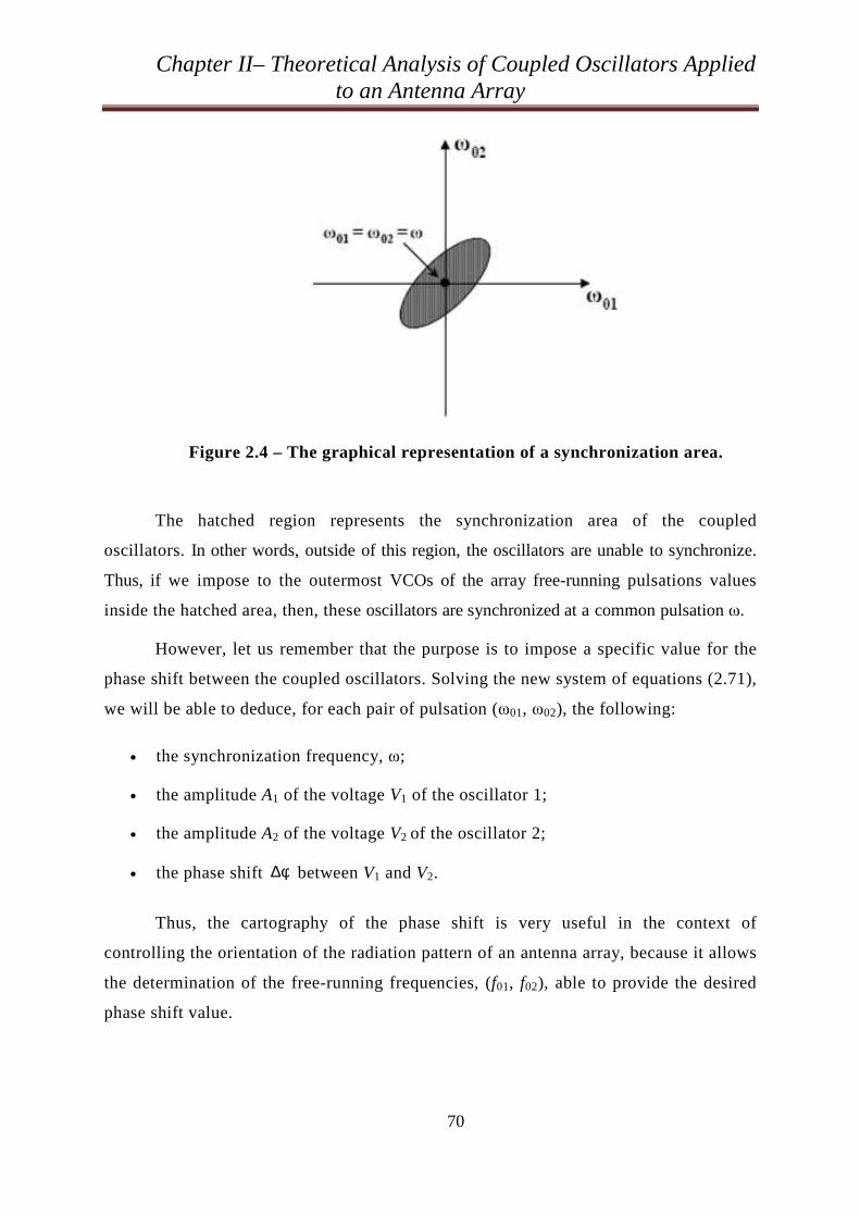
Chapter II– Theoretical Analysis of Coupled Oscillators Applied to an Antenna Array
70
Figure 2.4 – The graphical representation of a synchronization area.
The hatched region represents the synchronization area of the coupled
oscillators. In other words, outside of this region, the oscillators are unable to synchronize.
Thus, if we impose to the outermost VCOs of the array free-running pulsations values
inside the hatched area, then, these oscillators are synchronized at a common pulsation ω.
However, let us remember that the purpose is to impose a specific value for the
phase shift between the coupled oscillators. Solving the new system of equations (2.71),
we will be able to deduce, for each pair of pulsation (ω01, ω02), the following:
• the synchronization frequency, ω;
• the amplitude A1 of the voltage V1 of the oscillator 1;
• the amplitude A2 of the voltage V2 of the oscillator 2;
• the phase shift φ∆ between V1 and V2.
Thus, the cartography of the phase shift is very useful in the context of
controlling the orientation of the radiation pattern of an antenna array, because it allows
the determination of the free-running frequencies, (f01, f02), able to provide the desired
phase shift value.
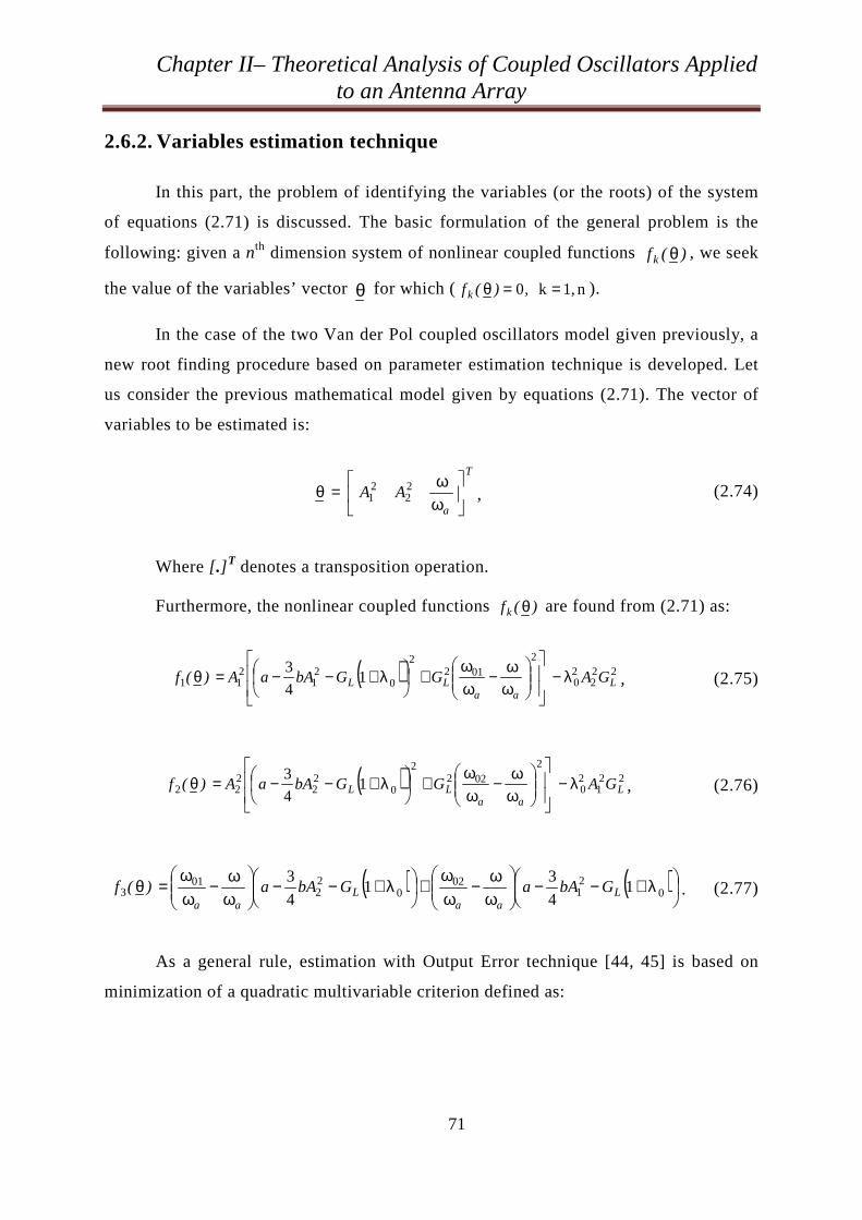
Chapter II– Theoretical Analysis of Coupled Oscillators Applied to an Antenna Array
71
2.6.2. Variables estimation technique
In this part, the problem of identifying the variables (or the roots) of the system
of equations (2.71) is discussed. The basic formulation of the general problem is the
following: given a nth dimension system of nonlinear coupled functions )(fk θ , we seek
the value of the variables’ vector θ for which ( n1,k 0 ==θ ,)(fk ).
In the case of the two Van der Pol coupled oscillators model given previously, a
new root finding procedure based on parameter estimation technique is developed. Let
us consider the previous mathematical model given by equations (2.71). The vector of
variables to be estimated is:
T
a
AA
ωω=θ 2
221 , (2.74)
Where [ .] T denotes a transposition operation.
Furthermore, the nonlinear coupled functions )(fk θ are found from (2.71) as:
( ) 222
20
2012
2
021
211 1
4
3 L
aaLL GAGGbAaA)(f λ−
ωω−
ωω
+
λ+−−=θ , (2.75)
( ) 221
20
2022
2
022
222 1
4
3 L
aaLL GAGGbAaA)(f λ−
ωω−
ωω
+
λ+−−=θ , (2.76)
( ) ( )
λ+−−
ωω−
ωω
+
λ+−−
ωω−
ωω
=θ 021
020
22
013 1
4
3 1
4
3 L
aaL
aa
GbAaGbAa)(f . (2.77)
As a general rule, estimation with Output Error technique [44, 45] is based on
minimization of a quadratic multivariable criterion defined as:
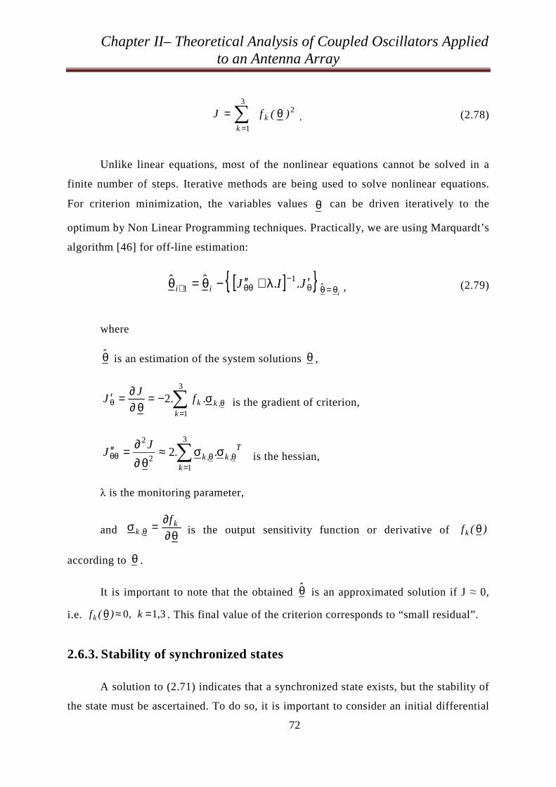
Chapter II– Theoretical Analysis of Coupled Oscillators Applied to an Antenna Array
72
∑=
θ=3
1
2
kk )(fJ . (2.78)
Unlike linear equations, most of the nonlinear equations cannot be solved in a
finite number of steps. Iterative methods are being used to solve nonlinear equations.
For criterion minimization, the variables values θ can be driven iteratively to the
optimum by Non Linear Programming techniques. Practically, we are using Marquardt’s
algorithm [46] for off-line estimation:
[ ] i
ˆii J.I.Jˆˆθ=θθ
−θθ+ ′λ+′′−θ=θ
1
1 , (2.79)
where
θ is an estimation of the system solutions θ ,
∑=
θθ σ−=θ∂
∂=′3
1
2k
,kk .f.J
J is the gradient of criterion,
∑=
θθθθ σσ≈θ∂
∂=′′3
12
2
2k
T,k,k ..
JJ is the hessian,
λ is the monitoring parameter,
and θ∂∂=σ θ
k,k
f is the output sensitivity function or derivative of )(fk θ
according to θ .
It is important to note that the obtained θ is an approximated solution if J ≈ 0,
i.e. 1,3 0 =≈θ k,)(fk . This final value of the criterion corresponds to “small residual”.
2.6.3. Stability of synchronized states
A solution to (2.71) indicates that a synchronized state exists, but the stability of
the state must be ascertained. To do so, it is important to consider an initial differential
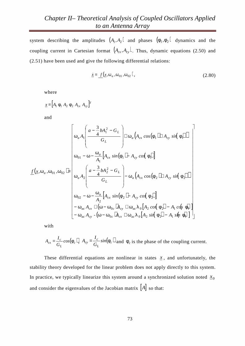
Chapter II– Theoretical Analysis of Coupled Oscillators Applied to an Antenna Array
73
system describing the amplitudes ( )21 A,A and phases ( )21 φφ , dynamics and the
coupling current in Cartesian format ( )cycx A,A . Thus, dynamic equations (2.50) and
(2.51) have been used and give the following differential relations:
( )0201 ωωω= ,,,xfx a , (2.80)
where
[ ]Tcycx AAAAx 2211 φφ=
and
( )
( ) ( )( )
( ) ( )[ ]
( ) ( )( )
( ) ( )[ ]( ) ( ) ( )[ ]( ) ( ) ( )[ ]
φ−φλω+ω−ωω−
φ−φλω+ω−ω+ω−
φ−φω
−ω−ω
φ+φω−
−−ω
φ−φω
−ω−ω
φ+φω+
−−ω
=ωωω
112200
112200
222
02
22
22
2
111
01
11
21
1
0201
-
4
3
4
3
sinAsinAAA
cosAcosAAA
cosAsinAA
sinAcosAG
GbAaA
cosAsinAA
sinAcosAG
GbAaA
,,,xf
accxccyac
accyccxac
cycxa
cycxaL
L
a
cycxa
cycxaL
L
a
a
with
( )cL
ccx cos
G
IA φ= , ( )c
L
ccy sin
G
IA φ= and cφ is the phase of the coupling current.
These differential equations are nonlinear in states x , and unfortunately, the
stability theory developed for the linear problem does not apply directly to this system.
In practice, we typically linearize this system around a synchronized solution noted 0x
and consider the eigenvalues of the Jacobian matrix [ ]A so that:
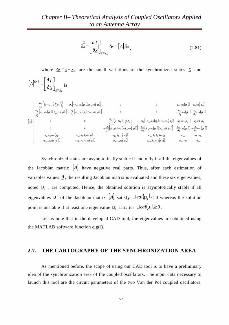
Chapter II– Theoretical Analysis of Coupled Oscillators Applied to an Antenna Array
74
[ ] x.Ax.x
fx
xx
δ=δ
∂∂
=δ=
⋅
0
, (2.81)
where 0 xxx −=δ are the small variations of the synchronized states x and
[ ]0
66
xxx
fA
=
×
∂∂
= is
[ ]
( ) ( ) ( )[ ] ( ) ( )
( ) ( )[ ] ( ) ( )[ ] ( ) ( )
( ) ( ) ( )[ ] ( ) ( )
( ) ( )[ ] ( ) ( )[ ] ( ) ( )( ) ( ) ( ) ( )( ) ( ) ( ) ( )
−−−−
−−−−
−+−−
−−+−−
−−
−+−−
+−
−−
=
accacacacac
cacacacacac
aacycx
acycx
a
aacycxaLL
a
aacycx
acycx
a
aacycxaLL
a
AA
AA
AAAA
AAA
A
AAbAGaG
AAAA
AAA
A
AAbAGaG
A
ωωωφλωφλωφλωφλω
ωωωφλωφλωφλωφλω
φω
φω
φφω
φφω
φωφωφφωω
φω
φω
φφω
φφω
φωφωφφωω
02202011010
02202011010
22
22
222
2222
222222
11
11
111
1121
111121
cossincossin
sincossincos
cos sinsin coscos sin 00
sincoscos sin49 00
cossin 00sin cos cos sin
sincos00cos sin49
Synchronized states are asymptotically stable if and only if all the eigenvalues of
the Jacobian matrix [ ]A have negative real parts. Thus, after each estimation of
variables values θ , the resulting Jacobian matrix is evaluated and these six eigenvalues,
noted iµ , are computed. Hence, the obtained solution is asymptotically stable if all
eigenvalues iµ of the Jacobian matrix [ ]A satisfy ( )ieal µℜ < 0 whereas the solution
point is unstable if at least one eigenvalue iµ satisfies ( ) 0 ≥µℜ ieal .
Let us note that in the developed CAD tool, the eigenvalues are obtained using
the MATLAB software function eig(⋅).
2.7. THE CARTOGRAPHY OF THE SYNCHRONIZATION AREA
As mentioned before, the scope of using our CAD tool is to have a preliminary
idea of the synchronization area of the coupled oscillators. The input data necessary to
launch this tool are the circuit parameters of the two Van der Pol coupled oscillators.
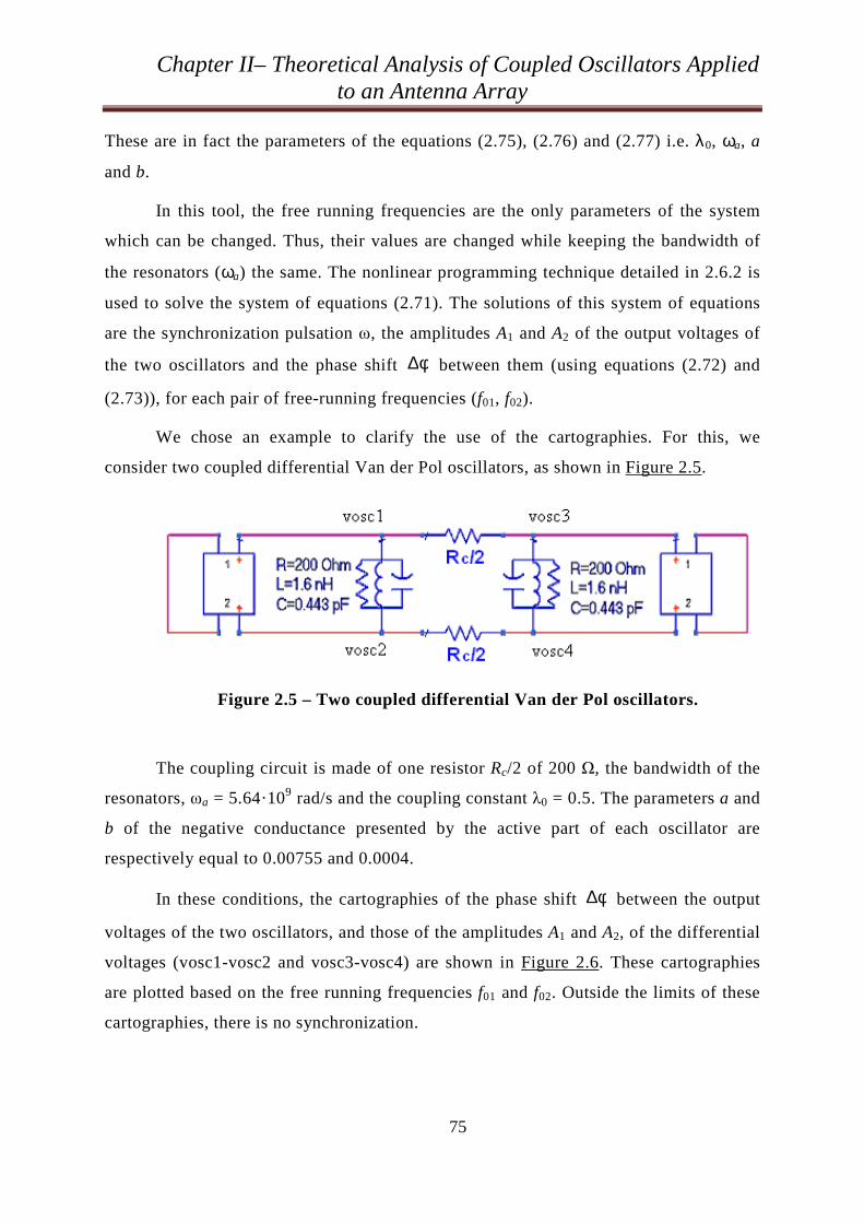
Chapter II– Theoretical Analysis of Coupled Oscillators Applied to an Antenna Array
75
These are in fact the parameters of the equations (2.75), (2.76) and (2.77) i.e. λ0, ωa, a
and b.
In this tool, the free running frequencies are the only parameters of the system
which can be changed. Thus, their values are changed while keeping the bandwidth of
the resonators (ωa) the same. The nonlinear programming technique detailed in 2.6.2 is
used to solve the system of equations (2.71). The solutions of this system of equations
are the synchronization pulsation ω, the amplitudes A1 and A2 of the output voltages of
the two oscillators and the phase shift φ∆ between them (using equations (2.72) and
(2.73)), for each pair of free-running frequencies (f01, f02).
We chose an example to clarify the use of the cartographies. For this, we
consider two coupled differential Van der Pol oscillators, as shown in Figure 2.5.
Figure 2.5 – Two coupled differential Van der Pol oscillators.
The coupling circuit is made of one resistor Rc/2 of 200 , the bandwidth of the
resonators, ωa = 5.64·109 rad/s and the coupling constant λ0 = 0.5. The parameters a and
b of the negative conductance presented by the active part of each oscillator are
respectively equal to 0.00755 and 0.0004.
In these conditions, the cartographies of the phase shift φ∆ between the output
voltages of the two oscillators, and those of the amplitudes A1 and A2, of the differential
voltages (vosc1-vosc2 and vosc3-vosc4) are shown in Figure 2.6. These cartographies
are plotted based on the free running frequencies f01 and f02. Outside the limits of these
cartographies, there is no synchronization.
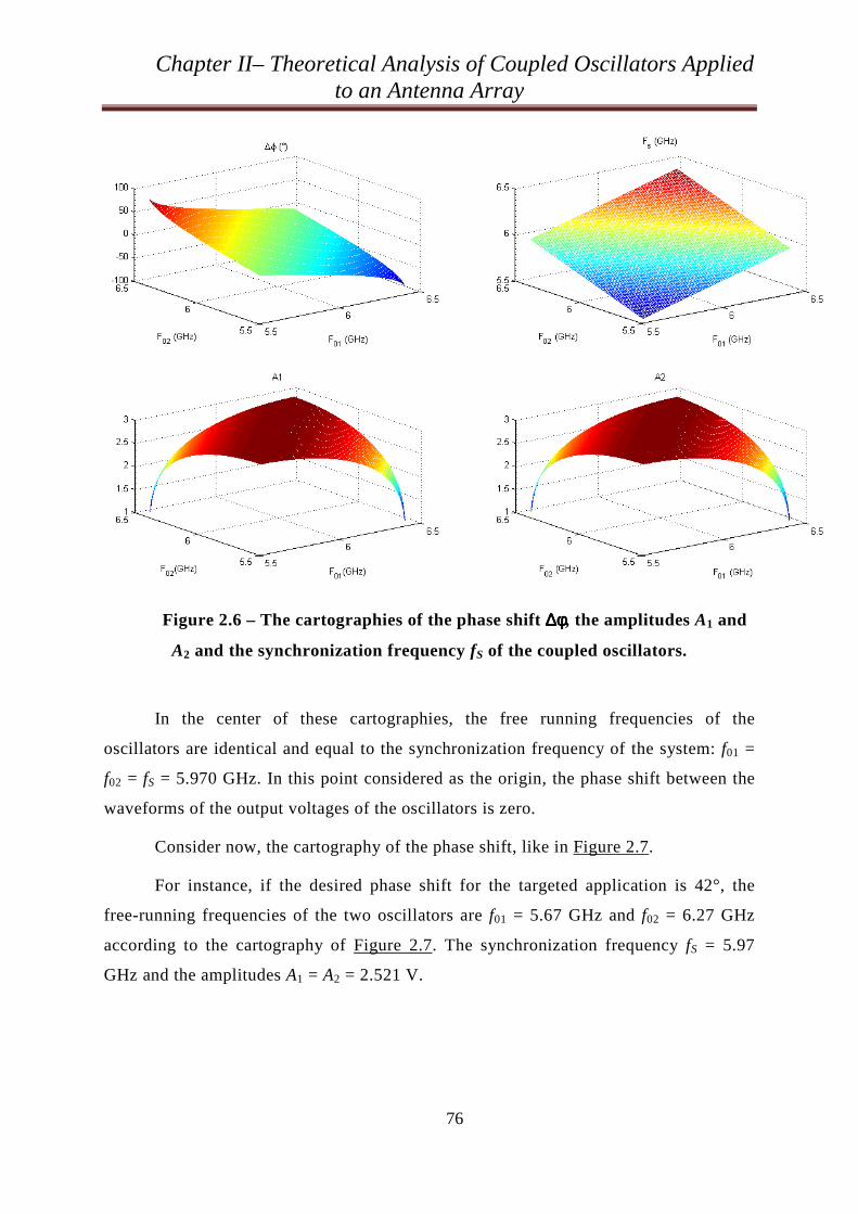
Chapter II– Theoretical Analysis of Coupled Oscillators Applied to an Antenna Array
76
Figure 2.6 – The cartographies of the phase shift ∆∆∆∆φφφφ, the amplitudes A1 and
A2 and the synchronization frequency fS of the coupled oscillators.
In the center of these cartographies, the free running frequencies of the
oscillators are identical and equal to the synchronization frequency of the system: f01 =
f02 = fS = 5.970 GHz. In this point considered as the origin, the phase shift between the
waveforms of the output voltages of the oscillators is zero.
Consider now, the cartography of the phase shift, like in Figure 2.7.
For instance, if the desired phase shift for the targeted application is 42°, the
free-running frequencies of the two oscillators are f01 = 5.67 GHz and f02 = 6.27 GHz
according to the cartography of Figure 2.7. The synchronization frequency fS = 5.97
GHz and the amplitudes A1 = A2 = 2.521 V.
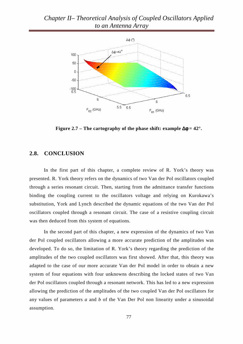
Chapter II– Theoretical Analysis of Coupled Oscillators Applied to an Antenna Array
77
Figure 2.7 – The cartography of the phase shift: example ∆∆∆∆φφφφ = 42°.
2.8. CONCLUSION
In the first part of this chapter, a complete review of R. York’s theory was
presented. R. York theory refers on the dynamics of two Van der Pol oscillators coupled
through a series resonant circuit. Then, starting from the admittance transfer functions
binding the coupling current to the oscillators voltage and relying on Kurokawa’s
substitution, York and Lynch described the dynamic equations of the two Van der Pol
oscillators coupled through a resonant circuit. The case of a resistive coupling circuit
was then deduced from this system of equations.
In the second part of this chapter, a new expression of the dynamics of two Van
der Pol coupled oscillators allowing a more accurate prediction of the amplitudes was
developed. To do so, the limitation of R. York’s theory regarding the prediction of the
amplitudes of the two coupled oscillators was first showed. After that, this theory was
adapted to the case of our more accurate Van der Pol model in order to obtain a new
system of four equations with four unknowns describing the locked states of two Van
der Pol oscillators coupled through a resonant network. This has led to a new expression
allowing the prediction of the amplitudes of the two coupled Van der Pol oscillators for
any values of parameters a and b of the Van Der Pol non linearity under a sinusoidal
assumption.
Chapter II– Theoretical Analysis of Coupled Oscillators Applied to an Antenna Array
78
In the last part of this chapter, mathematical manipulations were applied to the
system of nonlinear equations describing the locked states of two Van der Pol
oscillators coupled through a resonant network as well as through a resistive one. A
simpler system of three equations with three unknowns was obtained allowing then to
implement a CAD tool that permits to extract the locking region of the coupled
oscillators, in an extremely short simulation time. This new system of equations was
solved on Matlab using nonlinear programming technique and the stability of the
synchronized states was also analyzed. Finally, an example of 3D graphic of the
synchronization area for two differential Van der Pol oscillators coupled through a
resistive network was showed. Thus, with this cartography and with the precise free-
running frequencies, it was possible to extract the value of the phase shift between the
output voltages of the oscillators as well as their amplitudes.
79
CHAPTER III
Study and Analysis of an Array of Differential
Oscillators and VCOs Coupled Through a Resistive
Network
Chapter III– Study and Analysis of an Array of Differential Oscillators and VCOs Coupled through a Resistive Network
80
3.1. INTRODUCTION
In the previous chapter, a new CAD tool which provides, in a considerably short
analysis time a cartography giving the phase shifts, synchronization frequencies and
amplitudes of the differential output voltages of two differential oscillators coupled
through a broadband network was presented. Indeed, as mentioned previously, it seems
to be interesting to analyze the behavior of an array of coupled differential oscillators
and VCOs since, in this case, the theoretical limit of the phase shift is within 360o due
to the differential nature of the array. Furthermore, the use of a broadband coupling
network, i.e. a resistor, instead of a resonant one, can lead to a substantial save in chip
area in the case of RF integrated circuit design.
Hence, in the first part of this chapter we will consider the case of the analysis of
two coupled differential oscillators. Since the theory implemented in our CAD tool uses
Van der Pol oscillators to model microwave coupled oscillators, a modeling procedure
of the differential oscillator as a differential Van der Pol oscillator will be presented.
Then, the proposed CAD tool was used in order to obtain the cartography of the
oscillators’ locked-states. This cartography can help the designer to rapidly find the free-
running frequencies of the two outermost VCOs of the array required to achieve the desired
phase shift. After that, in order to validate the results provided by our CAD tool, we
compared them to the simulation results of the two coupled differential oscillators
obtained with Agilent’s ADS software for different cases of coupling strength.
In the second part of this chapter, the same study was performed for the case of
two coupled differential Voltage Controlled Oscillators (VCOs. Furthermore, a new
analysis based on state equations method will be presented. The study of the variation
of the phase shift versus the coupling resistor will also be investigated as well as the
effect of a mismatch between the two coupling resistors on the phase shift. Finally, the
behavior of four coupled differential VCOs will be presented.
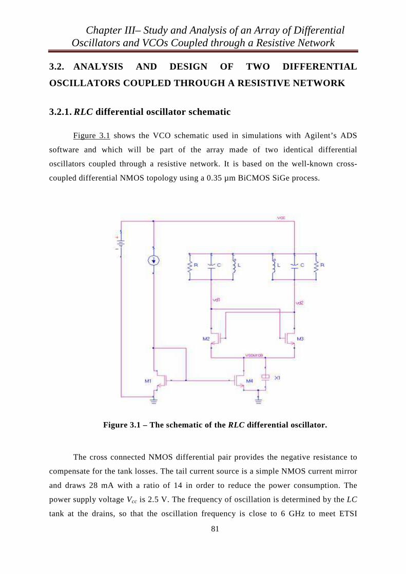
Chapter III– Study and Analysis of an Array of Differential Oscillators and VCOs Coupled through a Resistive Network
81
3.2. ANALYSIS AND DESIGN OF TWO DIFFERENTIAL
OSCILLATORS COUPLED THROUGH A RESISTIVE NETWORK
3.2.1. RLC differential oscillator schematic
Figure 3.1 shows the VCO schematic used in simulations with Agilent’s ADS
software and which will be part of the array made of two identical differential
oscillators coupled through a resistive network. It is based on the well-known cross-
coupled differential NMOS topology using a 0.35 µm BiCMOS SiGe process.
Figure 3.1 – The schematic of the RLC differential oscillator.
The cross connected NMOS differential pair provides the negative resistance to
compensate for the tank losses. The tail current source is a simple NMOS current mirror
and draws 28 mA with a ratio of 14 in order to reduce the power consumption. The
power supply voltage Vcc is 2.5 V. The frequency of oscillation is determined by the LC
tank at the drains, so that the oscillation frequency is close to 6 GHz to meet ETSI
Chapter III– Study and Analysis of an Array of Differential Oscillators and VCOs Coupled through a Resistive Network
82
(European Telecommunication Standard Institute) standard for ITS (Intelligent
Transport System requirements) for instance Appendix B.
In these conditions, the inductance value, L, is close to 0.8 nH and the capacitor
value, C, is close to 0.88 pF. The resistor value, R, is equal to 100 , so that the quality
factor of the tank is:
00
ωω
L
R R C Q == . (3.1)
Replacing the values for R, C, 0ω , the quality factor is equal to 3.3.
A tail capacitor, X1 of 20 pF, is used to attenuate both the high frequency noise
components of the tail-current and the voltage variation on the tail node. This latter
effect results in more symmetric waveforms and smaller harmonic distortion in LC-
VCO outputs [47].
To ensure proper start-up of the oscillator, the following condition needs to be
satisfied:
R gm1> .
(3.2)
In these conditions, the NMOS transistors sizes are identical and chosen to be:
m350
m70
.
L
w =
.
Figure 3.2 a shows the output voltages, vd1 and vd2, of the differential oscillator.
We can notice that they both have almost the same peak to peak amplitude, close to 3 V.
In these conditions, the frequency of oscillation is, 5.970 GHz, with a capacitor value of
0.88 pF, as shown in Figure 3.2 b.

Chapter III– Study and Analysis of an Array of Differential Oscillators and VCOs Coupled through a Resistive Network
83
a)
b)
Figure 3.2 – a) The waveforms of the output voltage of the differential
oscillator;
b) The output spectrum.
794.90
794.95
795.00
795.05
795.10
795.15
795.20
795.25
795.30
794.85
795.35
-2
-1
0
1
2
-3
3
time, nsec
vd1-
vd2
Chapter III– Study and Analysis of an Array of Differential Oscillators and VCOs Coupled through a Resistive Network
84
3.2.2. The modeling of the differential oscillator as a Van der Pol
oscillator
Since the theory implemented in our CAD tool “ASVAL” uses Van Der Pol
oscillators to model microwave coupled oscillators as explained in chapter 2, we
performed the modeling of the differential oscillator of Figure 3.1 as a differential Van
der Pol oscillator.
The modeling step is divided in two parts:
The modeling of the passive part which is represented by the resonator giving the
oscillation frequency;
The modeling of the active part, which includes the transistor that compensate
the losses.
3.2.2.1. The modeling of the passive part
The passive part corresponding to the resonator must be modeled by a parallel
RLC circuit. They must have the same behavior i.e. the same resonance frequency and
the same quality factor, within the frequency band of operation of the oscillator.
We set the parameters of the Van der Pol oscillator in order to ensure a
resonance frequency of the RLC circuit equal to the resonance frequency of the
differential oscillator’s resonator, like in Figure 3.3. In these conditions, the inductance
value, Lvp, is close to 1.6 nH, the capacitor value, Cvp, is close to 0.44 pF and the
resistor value, Rvp, is equal to 200 .
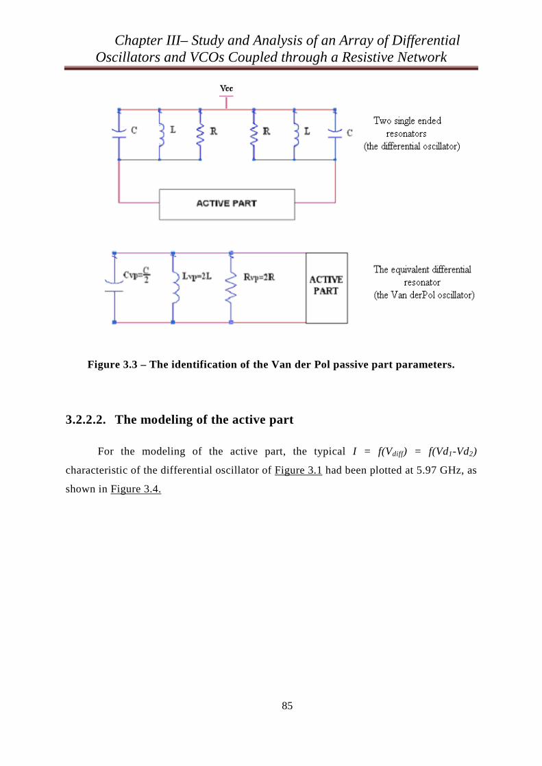
Chapter III– Study and Analysis of an Array of Differential Oscillators and VCOs Coupled through a Resistive Network
85
Figure 3.3 – The identification of the Van der Pol passive part parameters.
3.2.2.2. The modeling of the active part
For the modeling of the active part, the typical I = f(Vdiff) = f(Vd1-Vd2)
characteristic of the differential oscillator of Figure 3.1 had been plotted at 5.97 GHz, as
shown in Figure 3.4.
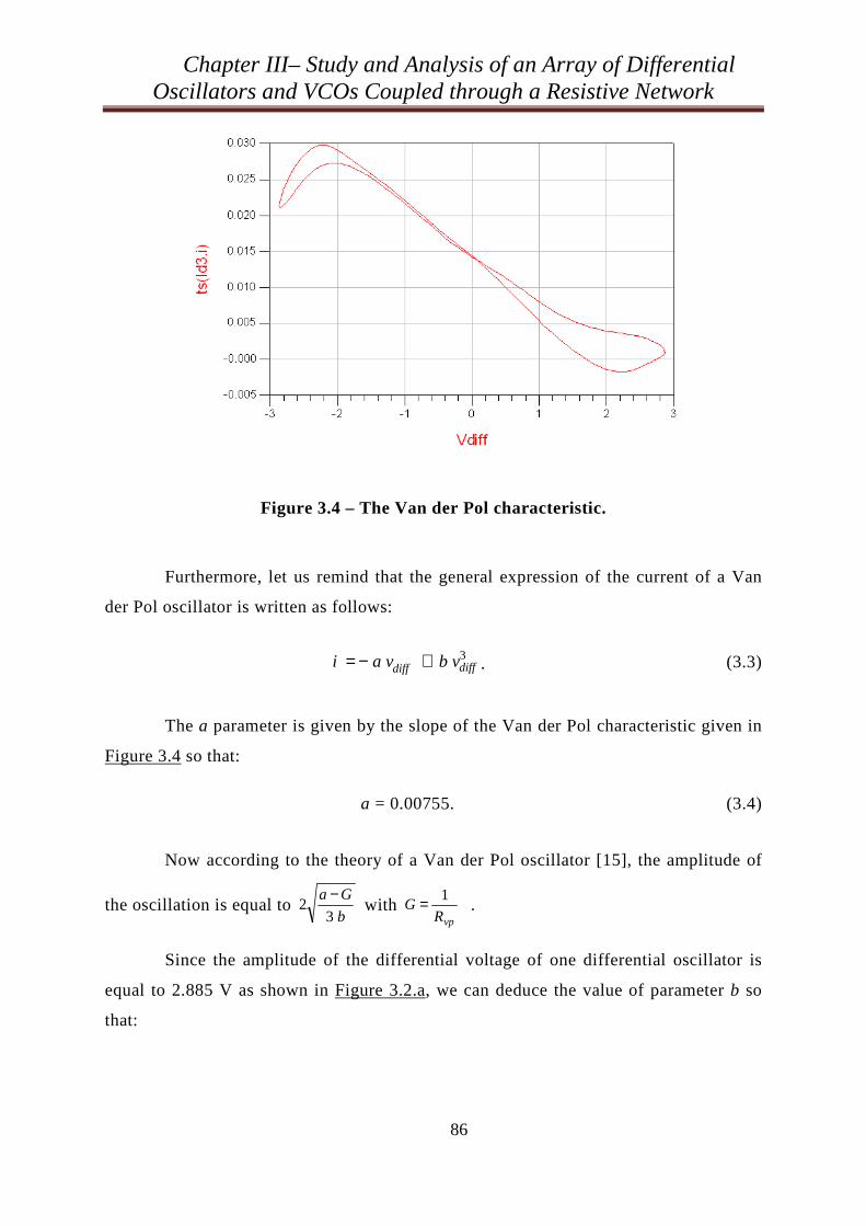
Chapter III– Study and Analysis of an Array of Differential Oscillators and VCOs Coupled through a Resistive Network
86
Figure 3.4 – The Van der Pol characteristic.
Furthermore, let us remind that the general expression of the current of a Van
der Pol oscillator is written as follows:
3diffdiff b v a vi +−= . (3.3)
The a parameter is given by the slope of the Van der Pol characteristic given in
Figure 3.4 so that:
a = 0.00755. (3.4)
Now according to the theory of a Van der Pol oscillator [15], the amplitude of
the oscillation is equal to b
Ga
32
− with
vpRG
1= .
Since the amplitude of the differential voltage of one differential oscillator is
equal to 2.885 V as shown in Figure 3.2.a, we can deduce the value of parameter b so
that:
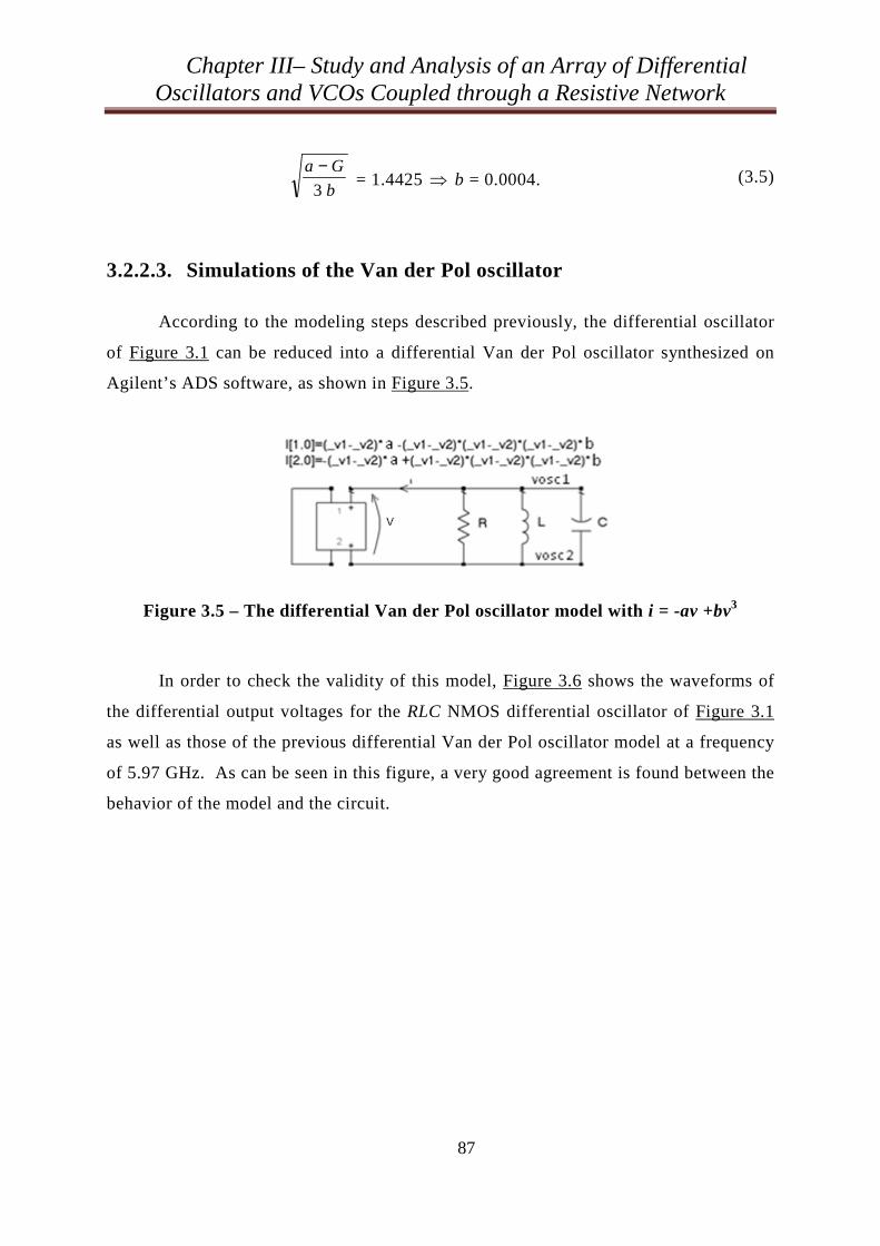
Chapter III– Study and Analysis of an Array of Differential Oscillators and VCOs Coupled through a Resistive Network
87
b
Ga
3
− = 1.4425 ⇒ b = 0.0004. (3.5)
3.2.2.3. Simulations of the Van der Pol oscillator
According to the modeling steps described previously, the differential oscillator
of Figure 3.1 can be reduced into a differential Van der Pol oscillator synthesized on
Agilent’s ADS software, as shown in Figure 3.5.
Figure 3.5 – The differential Van der Pol oscillator model with i = -av +bv3
In order to check the validity of this model, Figure 3.6 shows the waveforms of
the differential output voltages for the RLC NMOS differential oscillator of Figure 3.1
as well as those of the previous differential Van der Pol oscillator model at a frequency
of 5.97 GHz. As can be seen in this figure, a very good agreement is found between the
behavior of the model and the circuit.
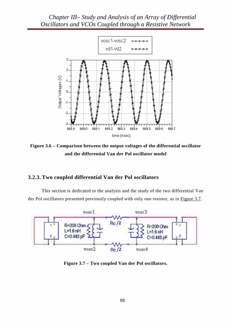
Chapter III– Study and Analysis of an Array of Differential Oscillators and VCOs Coupled through a Resistive Network
88
Figure 3.6 – Comparison between the output voltages of the differential oscillator
and the differential Van der Pol oscillator model
3.2.3. Two coupled differential Van der Pol oscillators
This section is dedicated to the analysis and the study of the two differential Van
der Pol oscillators presented previously coupled with only one resistor, as in Figure 3.7.
Figure 3.7 – Two coupled Van der Pol oscillators.
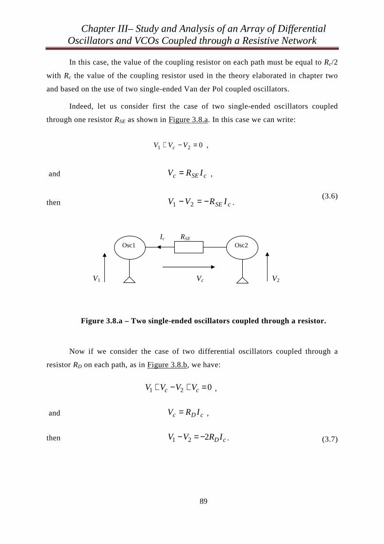
Chapter III– Study and Analysis of an Array of Differential Oscillators and VCOs Coupled through a Resistive Network
89
In this case, the value of the coupling resistor on each path must be equal to Rc/2
with Rc the value of the coupling resistor used in the theory elaborated in chapter two
and based on the use of two single-ended Van der Pol coupled oscillators.
Indeed, let us consider first the case of two single-ended oscillators coupled
through one resistor RSE as shown in Figure 3.8.a. In this case we can write:
021 =−+ VVV c ,
and cSEc IRV = ,
then cSEIRVV −=− 21 . (3.6)
Ic RSE
V1 Vc V2
Figure 3.8.a – Two single-ended oscillators coupled through a resistor.
Now if we consider the case of two differential oscillators coupled through a
resistor RD on each path, as in Figure 3.8.b, we have:
021 =+−+ cc VVVV ,
and cDc IRV = ,
then cD IRVV 221 −=− . (3.7)
Osc1 Osc2
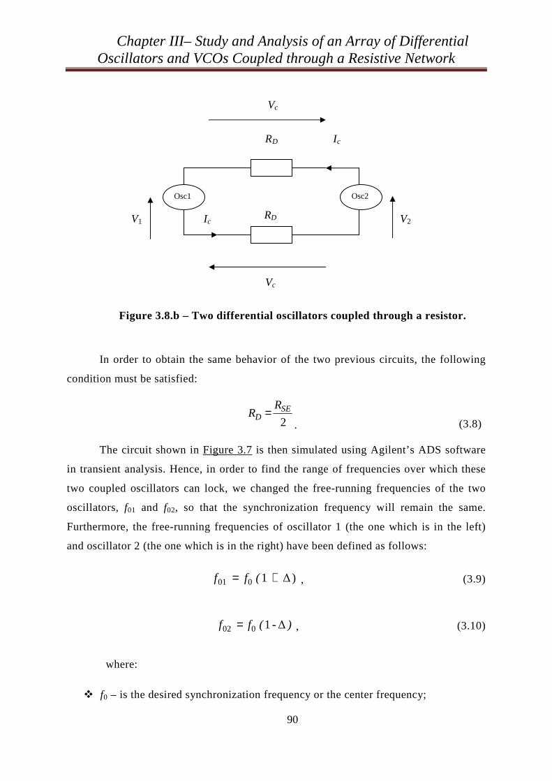
Chapter III– Study and Analysis of an Array of Differential Oscillators and VCOs Coupled through a Resistive Network
90
RD Ic
V1 Ic V2
Figure 3.8.b – Two differential oscillators coupled through a resistor.
In order to obtain the same behavior of the two previous circuits, the following
condition must be satisfied:
2SE
DR
R =. (3.8)
The circuit shown in Figure 3.7 is then simulated using Agilent’s ADS software
in transient analysis. Hence, in order to find the range of frequencies over which these
two coupled oscillators can lock, we changed the free-running frequencies of the two
oscillators, f01 and f02, so that the synchronization frequency will remain the same.
Furthermore, the free-running frequencies of oscillator 1 (the one which is in the left)
and oscillator 2 (the one which is in the right) have been defined as follows:
) 1001 ( f f += , (3.9)
) - ( f f 1002 = , (3.10)
where:
f0 – is the desired synchronization frequency or the center frequency;
RD
Vc
Vc
Osc1 Osc2
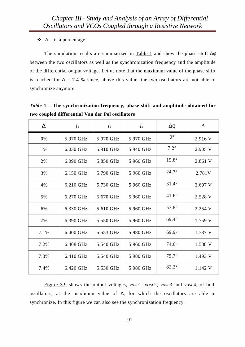
Chapter III– Study and Analysis of an Array of Differential Oscillators and VCOs Coupled through a Resistive Network
91
∆ - is a percentage.
The simulation results are summarized in Table 1 and show the phase shift ∆φ
between the two oscillators as well as the synchronization frequency and the amplitude
of the differential output voltage. Let us note that the maximum value of the phase shift
is reached for ∆ = 7.4 % since, above this value, the two oscillators are not able to
synchronize anymore.
Table 1 – The synchronization frequency, phase shift and amplitude obtained for
two coupled differential Van der Pol oscillators
∆ f1 f2 fs φ∆ A
0% 5.970 GHz 5.970 GHz 5.970 GHz 0° 2.916 V
1% 6.030 GHz 5.910 GHz 5.940 GHz 7.2° 2.905 V
2% 6.090 GHz 5.850 GHz 5.960 GHz 15.8° 2.861 V
3% 6.150 GHz 5.790 GHz 5.960 GHz 24.7° 2.781V
4% 6.210 GHz 5.730 GHz 5.960 GHz 31.4° 2.697 V
5% 6.270 GHz 5.670 GHz 5.960 GHz 41.6° 2.528 V
6% 6.330 GHz 5.610 GHz 5.960 GHz 53.8° 2.254 V
7% 6.390 GHz 5.550 GHz 5.960 GHz 69.4° 1.759 V
7.1% 6.400 GHz 5.553 GHz 5.980 GHz 69.9° 1.737 V
7.2% 6.408 GHz 5.540 GHz 5.960 GHz 74.6° 1.538 V
7.3% 6.410 GHz 5.540 GHz 5.980 GHz 75.7° 1.493 V
7.4% 6.420 GHz 5.530 GHz 5.980 GHz 82.2° 1.142 V
Figure 3.9 shows the output voltages, vosc1, vosc2, vosc3 and vosc4, of both
oscillators, at the maximum value of ∆, for which the oscillators are able to
synchronize. In this figure we can also see the synchronization frequency.
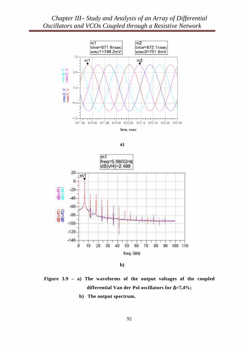
Chapter III– Study and Analysis of an Array of Differential Oscillators and VCOs Coupled through a Resistive Network
92
a)
b)
Figure 3.9 – a) The waveforms of the output voltages of the coupled
differential Van der Pol oscillators for ∆∆∆∆=7,4%;
b) The output spectrum.
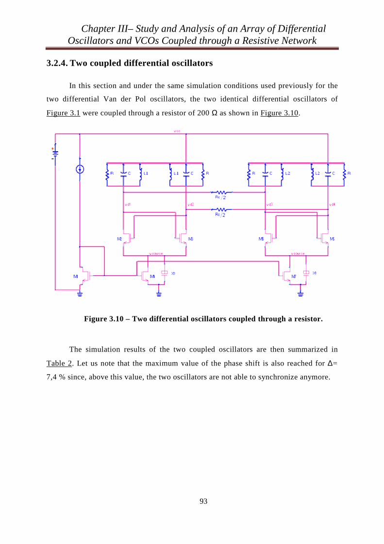
Chapter III– SOscillators and VC
3.2.4. Two coupled diffe
In this section and un
two differential Van der Po
Figure 3.1 were coupled thro
Figure 3.10 – Tw
The simulation result
Table 2. Let us note that the
7,4 % since, above this value
Study and Analysis of an Array of D VCOs Coupled through a Resistive
93
ifferential oscillators
under the same simulation conditions used p
Pol oscillators, the two identical different
rough a resistor of 200 Ω as shown in Figure
Two differential oscillators coupled throug
ults of the two coupled oscillators are the
the maximum value of the phase shift is als
lue, the two oscillators are not able to synchr
of Differential ive Network
d previously for the
ential oscillators of
ure 3.10.
ugh a resistor.
then summarized in
also reached for ∆=
hronize anymore.
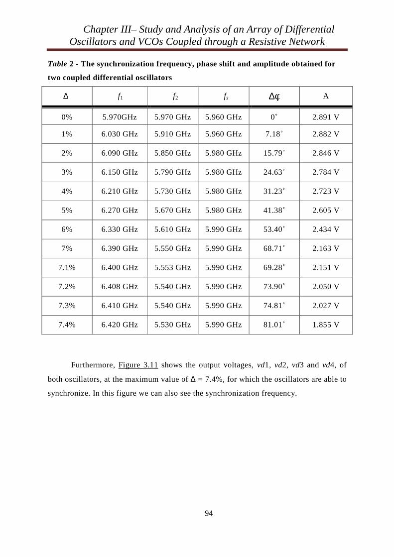
Chapter III– Study and Analysis of an Array of Differential Oscillators and VCOs Coupled through a Resistive Network
94
Table 2 - The synchronization frequency, phase shift and amplitude obtained for
two coupled differential oscillators
∆ f1 f2 fs φ∆ A
0% 5.970GHz 5.970 GHz 5.960 GHz 0˚ 2.891 V
1% 6.030 GHz 5.910 GHz 5.960 GHz 7.18˚ 2.882 V
2% 6.090 GHz 5.850 GHz 5.980 GHz 15.79˚ 2.846 V
3% 6.150 GHz 5.790 GHz 5.980 GHz 24.63˚ 2.784 V
4% 6.210 GHz 5.730 GHz 5.980 GHz 31.23˚ 2.723 V
5% 6.270 GHz 5.670 GHz 5.980 GHz 41.38˚ 2.605 V
6% 6.330 GHz 5.610 GHz 5.990 GHz 53.40˚ 2.434 V
7% 6.390 GHz 5.550 GHz 5.990 GHz 68.71˚ 2.163 V
7.1% 6.400 GHz 5.553 GHz 5.990 GHz 69.28˚ 2.151 V
7.2% 6.408 GHz 5.540 GHz 5.990 GHz 73.90˚ 2.050 V
7.3% 6.410 GHz 5.540 GHz 5.990 GHz 74.81˚ 2.027 V
7.4% 6.420 GHz 5.530 GHz 5.990 GHz 81.01˚ 1.855 V
Furthermore, Figure 3.11 shows the output voltages, vd1, vd2, vd3 and vd4, of
both oscillators, at the maximum value of ∆ = 7.4%, for which the oscillators are able to
synchronize. In this figure we can also see the synchronization frequency.
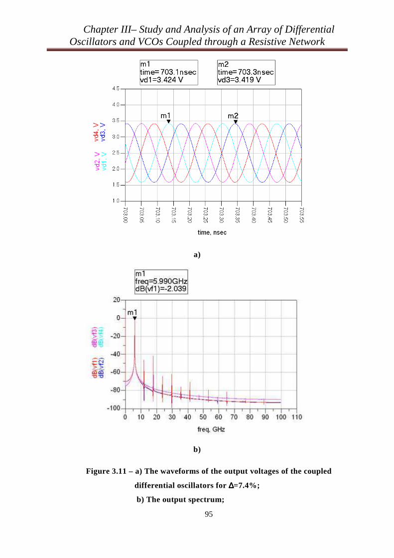
Chapter III– Study and Analysis of an Array of Differential Oscillators and VCOs Coupled through a Resistive Network
95
a)
b)
Figure 3.11 – a) The waveforms of the output voltages of the coupled
differential oscillators for ∆∆∆∆=7.4%;
b) The output spectrum;
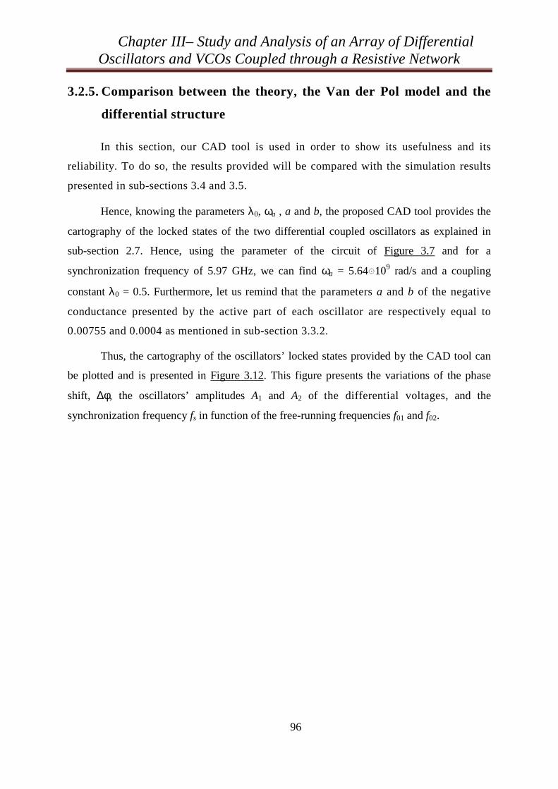
Chapter III– Study and Analysis of an Array of Differential Oscillators and VCOs Coupled through a Resistive Network
96
3.2.5. Comparison between the theory, the Van der Pol model and the
differential structure
In this section, our CAD tool is used in order to show its usefulness and its
reliability. To do so, the results provided will be compared with the simulation results
presented in sub-sections 3.4 and 3.5.
Hence, knowing the parameters λ0, ωa , a and b, the proposed CAD tool provides the
cartography of the locked states of the two differential coupled oscillators as explained in
sub-section 2.7. Hence, using the parameter of the circuit of Figure 3.7 and for a
synchronization frequency of 5.97 GHz, we can find ωa = 5.64 109 rad/s and a coupling
constant λ0 = 0.5. Furthermore, let us remind that the parameters a and b of the negative
conductance presented by the active part of each oscillator are respectively equal to
0.00755 and 0.0004 as mentioned in sub-section 3.3.2.
Thus, the cartography of the oscillators’ locked states provided by the CAD tool can
be plotted and is presented in Figure 3.12. This figure presents the variations of the phase
shift, ∆φ, the oscillators’ amplitudes A1 and A2 of the differential voltages, and the
synchronization frequency fs in function of the free-running frequencies f01 and f02.
Chapter III– Study and Analysis of an Array of Differential Oscillators and VCOs Coupled through a Resistive Network
97
Figure 3.12 - Cartography of the oscillators’ locked states provided by the CAD tool.
In order to validate the results provided by our CAD tool, we compared them to the
simulation results of the two coupled differential oscillators of Figure 3.10, obtained with
Agilent’s ADS software. Let us note that with ADS, only a transient analysis of one point at a
time of synchronization region allows to verify the synchronization results obtained with the
CAD tool. For instance, let us now consider Figure 3.12 where the point marked with an
arrow in the four subplots represents a free-running frequency f01 = 5.73 GHz for oscillator 1
and f02 = 6.21 GHz for oscillator 2. The marked points lead to a phase shift of 32.39°, a
synchronization frequency of the coupled oscillators of 5.97 GHz and an amplitude of 2.68 V
at the output of each of the coupled oscillators.

Chapter III– Study and Analysis of an Array of Differential Oscillators and VCOs Coupled through a Resistive Network
98
In the same conditions, the two differential NMOS coupled oscillators of Figure 3.10
simulated with ADS have lead to two sinusoidal waves at a synchronization frequency of
5.98 GHz, a phase shift of 31.23° and an amplitude of 2.72 V at the output of each oscillator,
as presented in Figure 3.13 and in Table 2.
Figure 3.13 – Waveforms of the output voltages of the two coupled differential NMOS
oscillators, when ∆∆∆∆φφφφ = 31.23° and A = 2.72 V
Furthermore, Figure 3.14 shows a comparison of the phase shift and amplitude
obtained for the coupled NMOS differential oscillators, the coupled differential Van der
Pol oscillators and by using “ASVAL”, for a synchronization frequency of 5.97 GHz, as
a function of 01020 fff −=∆ .
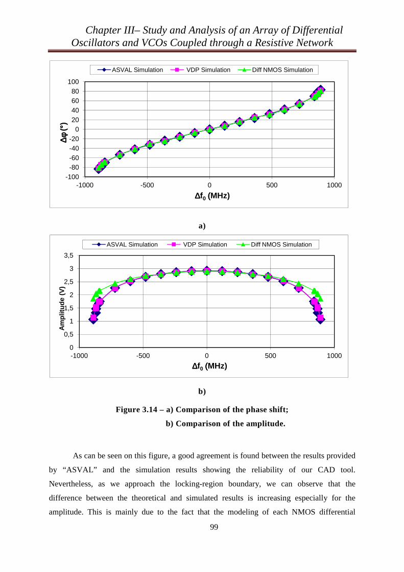
Chapter III– Study and Analysis of an Array of Differential Oscillators and VCOs Coupled through a Resistive Network
99
a)
b)
Figure 3.14 – a) Comparison of the phase shift;
b) Comparison of the amplitude.
As can be seen on this figure, a good agreement is found between the results provided
by “ASVAL” and the simulation results showing the reliability of our CAD tool.
Nevertheless, as we approach the locking-region boundary, we can observe that the
difference between the theoretical and simulated results is increasing especially for the
amplitude. This is mainly due to the fact that the modeling of each NMOS differential
-100-80-60-40-20
020406080
100
-1000 -500 0 500 1000
∆φ∆φ ∆φ∆φ( °° °°
)
∆∆∆∆f0 ((((MHz)
ASVAL Simulation VDP Simulation Diff NMOS Simulation
0
0,5
1
1,5
2
2,5
3
3,5
-1000 -500 0 500 1000
Am
plit
ud
e (V
)
∆∆∆∆f0 ((((MHz)
ASVAL Simulation VDP Simulation Diff NMOS Simulation
Chapter III– Study and Analysis of an Array of Differential Oscillators and VCOs Coupled through a Resistive Network
100
oscillator as a differential Van der Pol oscillator has been performed only at one frequency,
i.e. the desired synchronization frequency. The Figure 3.14.a shows that, as the oscillator
tunings are moved apart, but the synchronization frequency is halfway between, the phase
shift increases until the locking-region boundary is encountered. Concerning the prediction of
the amplitudes, we can say that the amplitude is at a minimum at the locking-region
boundaries (i.e. when the phase shift is at the extreme values) and equal to the oscillators’
free-running amplitude for equal tunings (i.e. when the phase shift is equal to zero).
Furthermore, let us remind that these simulations where performed for a coupling
constant λ0 = 0.5 for which the value of the coupling resistor Rc must be chosen equal to 400
Ω since the value of the parallel resistor R of the resonator is equal to 200 Ω. For this typical
value, York and Lynch proved in [19] that the locking-region is maximized while still
allowing the phase difference ∆φ to vary 180° over the locking range. Hence, this constitutes
an optimal value especially for beam-scanning systems where the designer wishes to
maximize the total phase variation and the locking-range simultaneously. Furthermore, let us
remind that, in the case studied here of two differential coupled oscillators, it is possible to
obtain a continuously controlled 360° phase shifting range due to the differential nature of the
system leading to a much more efficient beam-scanning architecture.
Nevertheless, in order to verify this affirmation, it seems interesting to study the
behavior of the system in both weak and strong coupling cases i.e. for values of λ0
respectively less and greater than 0.5.
3.2.6. Study and analysis of the two coupled differential oscillators in
the weak coupling case
In the weak coupling case, the circuits were analyzed for a value of the coupling
constant λ0 = 0.25 leading to Rc/2 = 400 . Thus, Figure 3.15 presents a comparison of
the phase shift and amplitude obtained for the two coupled Van der Pol oscillators, the
two coupled RLC NMOS differential oscillators and using “ASVAL” also for a
synchronization frequency of 5.97 GHz, as a function of 01020 fff −=∆ .

Chapter III– Study and Analysis of an Array of Differential Oscillators and VCOs Coupled through a Resistive Network
101
a)
b)
Figure 3.15 – The weak coupling case – a) Comparison of the phase shift;
b) Comparison of the amplitude.
As can be seen on this figure, the locking range as well as the maximum phase shift
which can be obtained are clearly reduced compared to the optimal case of a coupling
-80
-60
-40
-20
0
20
40
60
80
-400 -300 -200 -100 0 100 200 300 400
∆φ∆φ ∆φ∆φ( °° °°
)
∆∆∆∆f0 ((((MHz)
ASVAL Simulation VDP Simulation Diff NMOS Simulation
2,55
2,6
2,65
2,7
2,75
2,8
2,85
2,9
2,95
-400 -300 -200 -100 0 100 200 300 400
Am
plit
ud
e (V
)
∆∆∆∆f0 ((((MHz)
ASVAL Simulation VDP Simulation Diff NMOS Simulation
Chapter III– Study and Analysis of an Array of Differential Oscillators and VCOs Coupled through a Resistive Network
102
strength λ0 = 0.5. This result can be justified using the approximate formula (2.29). Indeed,
according to (2.29) we have:
aωλ<ω∆ 00 2 .
Hence, the locking range can be defined as:
amaxωλ=ω∆ 00 2 .
As a consequence, one can easily understand that the weak coupling case leads to a
smaller locking range of the system.
Furthermore, according to Figure 3.15.b, we can notice that the amplitude remains
close to its free-running value almost over the entire locking range. One more time, this
behavior can be justified using the approximate formula elaborated in chapter 2, i.e. (2.56).
Indeed, for small values of the coupling strength λ0, the expression (2.56) can be
approximated by ( )LGab
A −≅3
4 which represents the free-running amplitude of the Van
der Pol oscillator modelizing the behavior of the differential NMOS LC oscillator.
In Figure 3.16, the cartographies, obtained with “ASVAL”, of the phase shift ∆φ
between the output voltages of the two oscillators, and those of their amplitudes A1 and
A2, in the case of weak coupling are shown. Let us remind here that this cartography allows
to obtain the entire frequency locked states of the array of coupled oscillators.

Chapter III– SOscillators and VC
Figure 3.16 - The car
A2 and the synchronizati
3.2.7. Study and analys
the strong couplin
Let us now consider th
value of λ0 = 1.25 which imp
comparison of the obtained p
oscillators, two coupled RLC
a synchronization frequency
Study and Analysis of an Array of D VCOs Coupled through a Resistive
103
cartographies of the phase shift ∆∆∆∆φφφφ, the am
ation frequency fs of the coupled oscillator
coupling case
lysis of the two coupled differential
ling case
r the strong coupling case where the circuits w
mplies Rc/2 = 80 . In these conditions, Figu
d phase shift and amplitude for the two cou
NMOS differential oscillators and using “AS
cy of 5.97 GHz, as a function of 020 fff −=∆
of Differential ive Network
amplitudes A1 and
tors for the weak
ial oscillators in
were analyzed for a
igure 3.17 presents a
oupled Van der Pol
ASVAL” always for
01f .
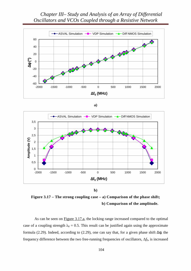
Chapter III– Study and Analysis of an Array of Differential Oscillators and VCOs Coupled through a Resistive Network
104
a)
b)
Figure 3.17 – The strong coupling case – a) Comparison of the phase shift;
b) Comparison of the amplitude.
As can be seen on Figure 3.17.a, the locking range increased compared to the optimal
case of a coupling strength λ0 = 0.5. This result can be justified again using the approximate
formula (2.29). Indeed, according to (2.29), one can say that, for a given phase shift ∆φ, the
frequency difference between the two free-running frequencies of oscillators, f0, is increased
-60
-40
-20
0
20
40
60
-2000 -1500 -1000 -500 0 500 1000 1500 2000
∆φ∆φ ∆φ∆φ( °° °°
)
∆∆∆∆f0 ((((MHz)
ASVAL Simulation VDP Simulation Diff NMOS Simulation
0
0,5
1
1,5
2
2,5
3
3,5
-2000 -1500 -1000 -500 0 500 1000 1500 2000
Am
plit
ud
e (V
)
∆∆∆∆f0 ((((MHz)
ASVAL Simulation VDP Simulation Diff NMOS Simulation
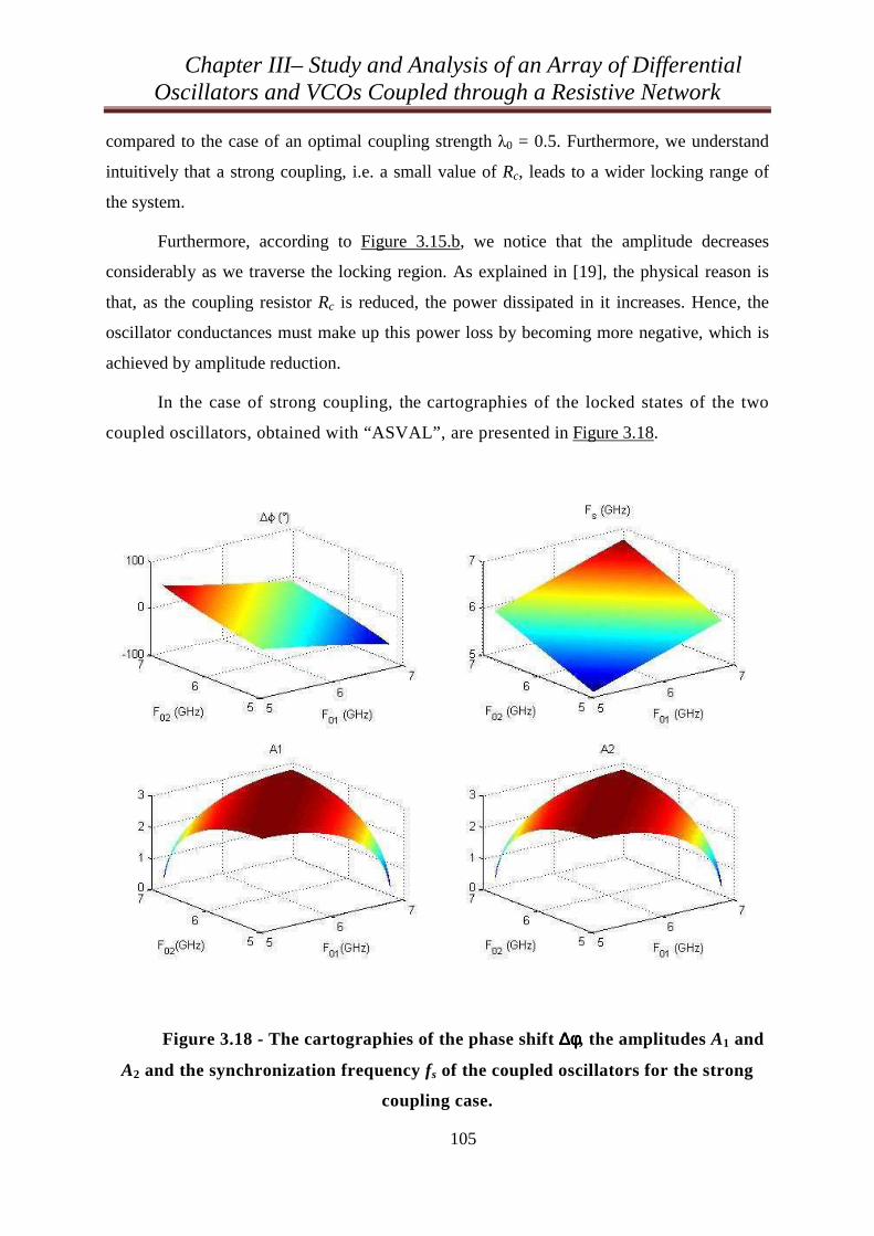
Chapter III– Study and Analysis of an Array of Differential Oscillators and VCOs Coupled through a Resistive Network
105
compared to the case of an optimal coupling strength λ0 = 0.5. Furthermore, we understand
intuitively that a strong coupling, i.e. a small value of Rc, leads to a wider locking range of
the system.
Furthermore, according to Figure 3.15.b, we notice that the amplitude decreases
considerably as we traverse the locking region. As explained in [19], the physical reason is
that, as the coupling resistor Rc is reduced, the power dissipated in it increases. Hence, the
oscillator conductances must make up this power loss by becoming more negative, which is
achieved by amplitude reduction.
In the case of strong coupling, the cartographies of the locked states of the two
coupled oscillators, obtained with “ASVAL”, are presented in Figure 3.18.
Figure 3.18 - The cartographies of the phase shift ∆∆∆∆φφφφ, the amplitudes A1 and
A2 and the synchronization frequency fs of the coupled oscillators for the strong
coupling case.
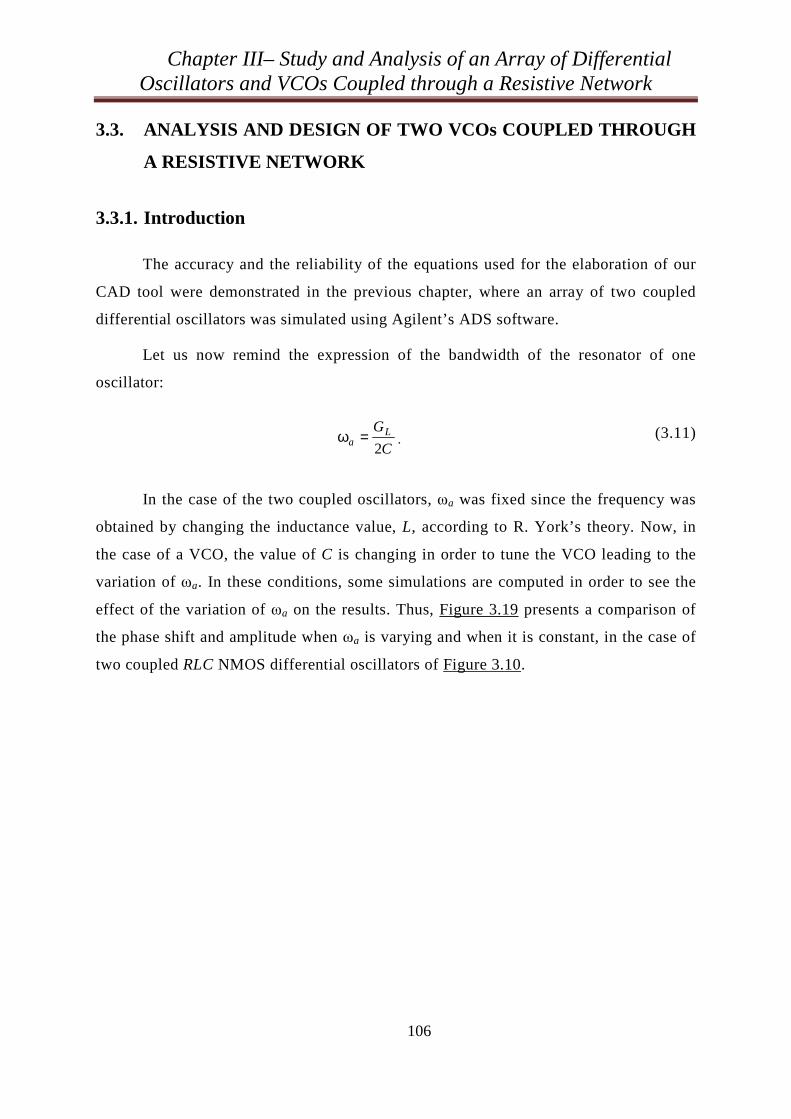
Chapter III– Study and Analysis of an Array of Differential Oscillators and VCOs Coupled through a Resistive Network
106
3.3. ANALYSIS AND DESIGN OF TWO VCOs COUPLED THROUGH
A RESISTIVE NETWORK
3.3.1. Introduction
The accuracy and the reliability of the equations used for the elaboration of our
CAD tool were demonstrated in the previous chapter, where an array of two coupled
differential oscillators was simulated using Agilent’s ADS software.
Let us now remind the expression of the bandwidth of the resonator of one
oscillator:
C
GLa 2
=ω . (3.11)
In the case of the two coupled oscillators, ωa was fixed since the frequency was
obtained by changing the inductance value, L, according to R. York’s theory. Now, in
the case of a VCO, the value of C is changing in order to tune the VCO leading to the
variation of ωa. In these conditions, some simulations are computed in order to see the
effect of the variation of ωa on the results. Thus, Figure 3.19 presents a comparison of
the phase shift and amplitude when ωa is varying and when it is constant, in the case of
two coupled RLC NMOS differential oscillators of Figure 3.10.
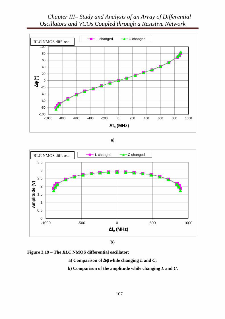
Chapter III– Study and Analysis of an Array of Differential Oscillators and VCOs Coupled through a Resistive Network
107
a)
b)
Figure 3.19 – The RLC NMOS differential oscillator:
a) Comparison of ∆∆∆∆φφφφ while changing L and C;
b) Comparison of the amplitude while changing L and C.
-100
-80
-60
-40
-20
0
20
40
60
80
100
-1000 -800 -600 -400 -200 0 200 400 600 800 1000
∆φ∆φ ∆φ∆φ( °° °°
)
∆∆∆∆f0 ((((MHz)
L changed C changed
0
0,5
1
1,5
2
2,5
3
3,5
-1000 -500 0 500 1000
Am
plit
ud
e (V
)
∆∆∆∆f0 ((((MHz)
L changed C changedRLC NMOS diff. osc.
RLC NMOS diff. osc.
Chapter III– Study and Analysis of an Array of Differential Oscillators and VCOs Coupled through a Resistive Network
108
In the same way, Figure 3.20 presents a comparison of the phase shift and amplitude
when ωa is varying and when it is constant, but in the case of two coupled Van der Pol
differential oscillators of Figure 3.7.
a)
b)
Figure 3.20 – The Van der Pol oscillator:
a) Comparison of ∆∆∆∆φφφφ while changing L and C;
b) Comparison of the amplitude while changing L and C.
-100
-80
-60
-40
-20
0
20
40
60
80
100
-1000 -800 -600 -400 -200 0 200 400 600 800 1000
∆φ∆φ ∆φ∆φ( °° °°
)
∆∆∆∆f0 ((((MHz)
L changed C changed
0
0,5
1
1,5
2
2,5
3
3,5
-1000 -800 -600 -400 -200 0 200 400 600 800 1000
Am
plit
ud
e (V
)
∆∆∆∆f0 ((((MHz)
L changed C changed
VAN der POL osc.
VAN der POL osc.

Chapter III– Study and Analysis of an Array of Differential Oscillators and VCOs Coupled through a Resistive Network
109
Since the variation of the resonator’s bandwidth doesn’t affect significantly the
results, ωa was kept constant for the following study and modeling of an array of two
differential LC VCOs. Hence, in our CAD tool, which can plot the cartography of the
synchronization area of two coupled VCOs, the value of ωa which will be used will
correspond to the capacitor value of the resonator leading to 0 0 =∆f .
3.3.2. The LC VCO architecture
The VCO’s schematic used in simulations is illustrated in Figure 3.21. The VCO
structure is also based on a crossed-coupled NMOS differential topology using a 0.35 m
BiCMOS SiGe process. Let us remind that, this VCO architecture is widely used in high-
frequency circuit design due to its relatively good phase noise performances and ease of
integration.
Figure 3.21 – The LC VCO schematic.
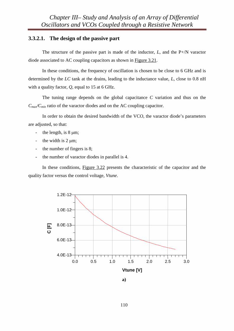
Chapter III– Study and Analysis of an Array of Differential Oscillators and VCOs Coupled through a Resistive Network
110
3.3.2.1. The design of the passive part
The structure of the passive part is made of the inductor, L, and the P+/N varactor
diode associated to AC coupling capacitors as shown in Figure 3.21.
In these conditions, the frequency of oscillation is chosen to be close to 6 GHz and is
determined by the LC tank at the drains, leading to the inductance value, L, close to 0.8 nH
with a quality factor, Q, equal to 15 at 6 GHz.
The tuning range depends on the global capacitance C variation and thus on the
Cmax/Cmin ratio of the varactor diodes and on the AC coupling capacitor.
In order to obtain the desired bandwidth of the VCO, the varactor diode’s parameters
are adjusted, so that:
- the length, is 8 m;
- the width is 2 m;
- the number of fingers is 8;
- the number of varactor diodes in parallel is 4.
In these conditions, Figure 3.22 presents the characteristic of the capacitor and the
quality factor versus the control voltage, Vtune.
0.5 1.0 1.5 2.0 2.5 0.0 3.0
6.0E-13
8.0E-13
1.0E-12
4.0E-13
1.2E-12
Vtune [V]
C [
F]
a)
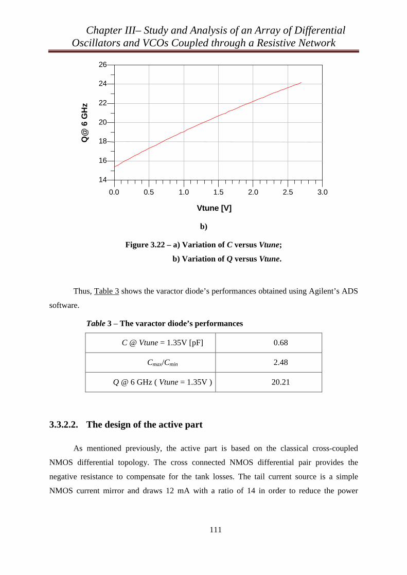
Chapter III– Study and Analysis of an Array of Differential Oscillators and VCOs Coupled through a Resistive Network
111
0.5 1.0 1.5 2.0 2.5 0.0 3.0
16
18
20
22
24
14
26
Vtune [V]
Q@
6 G
Hz
b)
Figure 3.22 – a) Variation of C versus Vtune;
b) Variation of Q versus Vtune.
Thus, Table 3 shows the varactor diode’s performances obtained using Agilent’s ADS
software.
Table 3 – The varactor diode’s performances
C @ Vtune = 1.35V [pF] 0.68
Cmax/Cmin 2.48
Q @ 6 GHz ( Vtune = 1.35V ) 20.21
3.3.2.2. The design of the active part
As mentioned previously, the active part is based on the classical cross-coupled
NMOS differential topology. The cross connected NMOS differential pair provides the
negative resistance to compensate for the tank losses. The tail current source is a simple
NMOS current mirror and draws 12 mA with a ratio of 14 in order to reduce the power
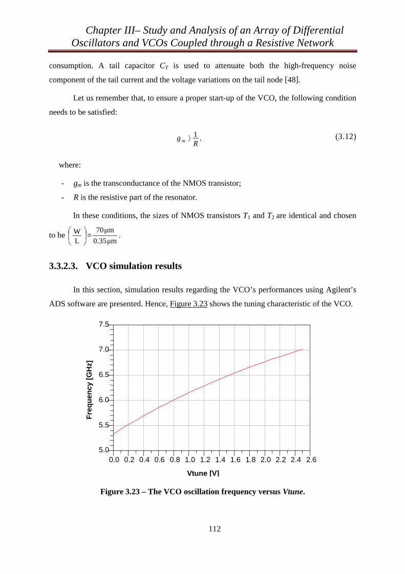
Chapter III– Study and Analysis of an Array of Differential Oscillators and VCOs Coupled through a Resistive Network
112
consumption. A tail capacitor CT is used to attenuate both the high-frequency noise
component of the tail current and the voltage variations on the tail node [48].
Let us remember that, to ensure a proper start-up of the VCO, the following condition
needs to be satisfied:
Rgm
1 ⟩ , (3.12)
where:
- gm is the transconductance of the NMOS transistor;
- R is the resistive part of the resonator.
In these conditions, the sizes of NMOS transistors T1 and T2 are identical and chosen
to be m35.0
m70
LW =
.
3.3.2.3. VCO simulation results
In this section, simulation results regarding the VCO’s performances using Agilent’s
ADS software are presented. Hence, Figure 3.23 shows the tuning characteristic of the VCO.
0.2 0.4 0.6 0.8 1.0 1.2 1.4 1.6 1.8 2.0 2.2 2.4 0.0 2.6
5.5
6.0
6.5
7.0
5.0
7.5
Vtune [V]
Fre
qu
ency
[G
Hz]
Figure 3.23 – The VCO oscillation frequency versus Vtune.
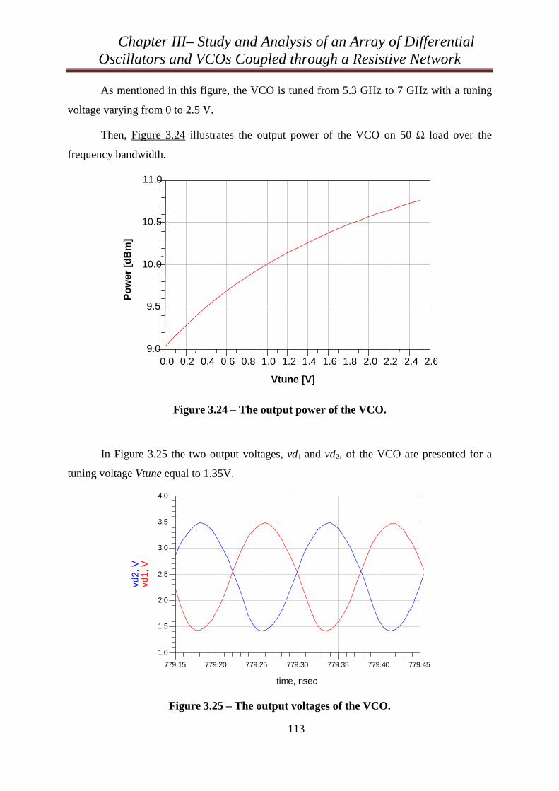
Chapter III– Study and Analysis of an Array of Differential Oscillators and VCOs Coupled through a Resistive Network
113
As mentioned in this figure, the VCO is tuned from 5.3 GHz to 7 GHz with a tuning
voltage varying from 0 to 2.5 V.
Then, Figure 3.24 illustrates the output power of the VCO on 50 load over the
frequency bandwidth.
0.2 0.4 0.6 0.8 1.0 1.2 1.4 1.6 1.8 2.0 2.2 2.4 0.0 2.6
9.5
10.0
10.5
9.0
11.0
Vtune [V]
Po
wer
[d
Bm
]
Figure 3.24 – The output power of the VCO.
In Figure 3.25 the two output voltages, vd1 and vd2, of the VCO are presented for a
tuning voltage Vtune equal to 1.35V.
Figure 3.25 – The output voltages of the VCO.
779.20 779.25 779.30 779.35 779.40779.15 779.45
1.5
2.0
2.5
3.0
3.5
1.0
4.0
time, nsec
vd1,
Vvd
2, V
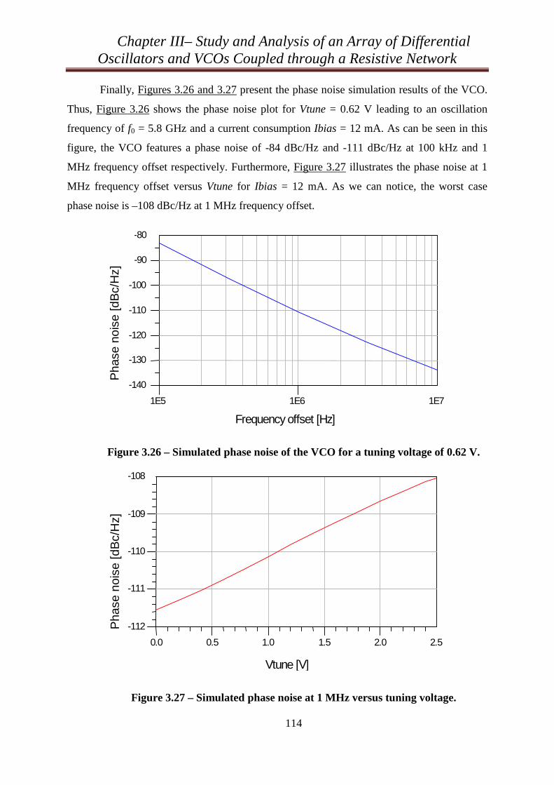
Chapter III– Study and Analysis of an Array of Differential Oscillators and VCOs Coupled through a Resistive Network
114
Finally, Figures 3.26 and 3.27 present the phase noise simulation results of the VCO.
Thus, Figure 3.26 shows the phase noise plot for Vtune = 0.62 V leading to an oscillation
frequency of f0 = 5.8 GHz and a current consumption Ibias = 12 mA. As can be seen in this
figure, the VCO features a phase noise of -84 dBc/Hz and -111 dBc/Hz at 100 kHz and 1
MHz frequency offset respectively. Furthermore, Figure 3.27 illustrates the phase noise at 1
MHz frequency offset versus Vtune for Ibias = 12 mA. As we can notice, the worst case
phase noise is –108 dBc/Hz at 1 MHz frequency offset.
1E6 1E5 1E7
-130
-120
-110
-100
-90
-140
-80
Frequency offset [Hz]
Pha
se n
oise
[dB
c/H
z]
Figure 3.26 – Simulated phase noise of the VCO for a tuning voltage of 0.62 V.
0.5 1.0 1.5 2.0 0.0 2.5
-111
-110
-109
-112
-108
Vtune [V]
Pha
se n
oise
[dB
c/H
z]
Figure 3.27 – Simulated phase noise at 1 MHz versus tuning voltage.
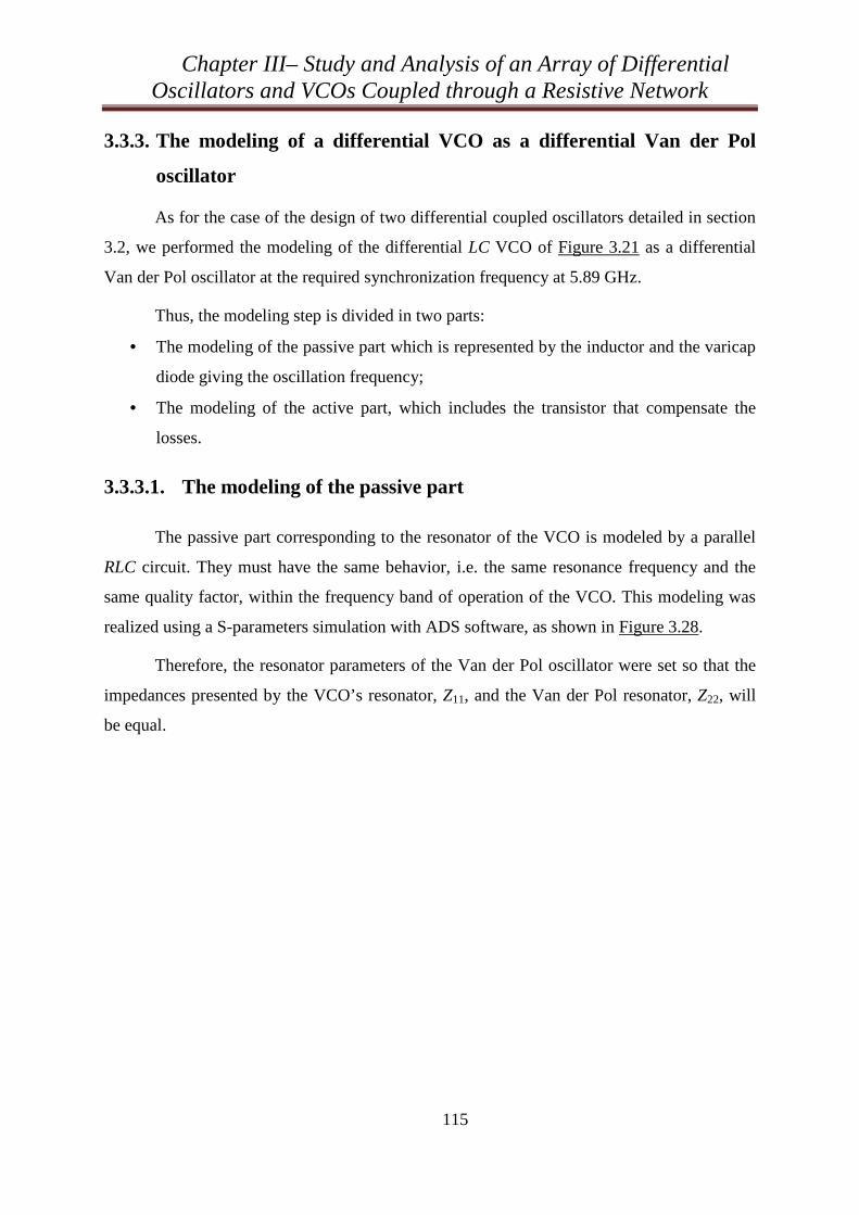
Chapter III– Study and Analysis of an Array of Differential Oscillators and VCOs Coupled through a Resistive Network
115
3.3.3. The modeling of a differential VCO as a differential Van der Pol
oscillator
As for the case of the design of two differential coupled oscillators detailed in section
3.2, we performed the modeling of the differential LC VCO of Figure 3.21 as a differential
Van der Pol oscillator at the required synchronization frequency at 5.89 GHz.
Thus, the modeling step is divided in two parts:
• The modeling of the passive part which is represented by the inductor and the varicap
diode giving the oscillation frequency;
• The modeling of the active part, which includes the transistor that compensate the
losses.
3.3.3.1. The modeling of the passive part
The passive part corresponding to the resonator of the VCO is modeled by a parallel
RLC circuit. They must have the same behavior, i.e. the same resonance frequency and the
same quality factor, within the frequency band of operation of the VCO. This modeling was
realized using a S-parameters simulation with ADS software, as shown in Figure 3.28.
Therefore, the resonator parameters of the Van der Pol oscillator were set so that the
impedances presented by the VCO’s resonator, Z11, and the Van der Pol resonator, Z22, will
be equal.
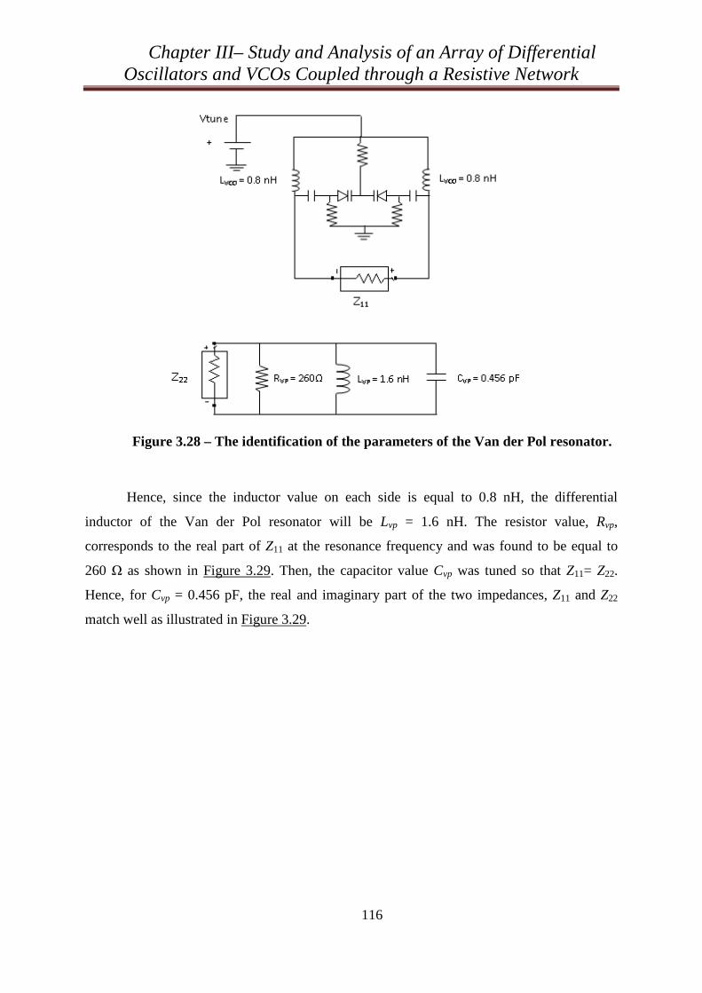
Chapter III– Study and Analysis of an Array of Differential Oscillators and VCOs Coupled through a Resistive Network
116
Figure 3.28 – The identification of the parameters of the Van der Pol resonator.
Hence, since the inductor value on each side is equal to 0.8 nH, the differential
inductor of the Van der Pol resonator will be Lvp = 1.6 nH. The resistor value, Rvp,
corresponds to the real part of Z11 at the resonance frequency and was found to be equal to
260 as shown in Figure 3.29. Then, the capacitor value Cvp was tuned so that Z11= Z22.
Hence, for Cvp = 0.456 pF, the real and imaginary part of the two impedances, Z11 and Z22
match well as illustrated in Figure 3.29.
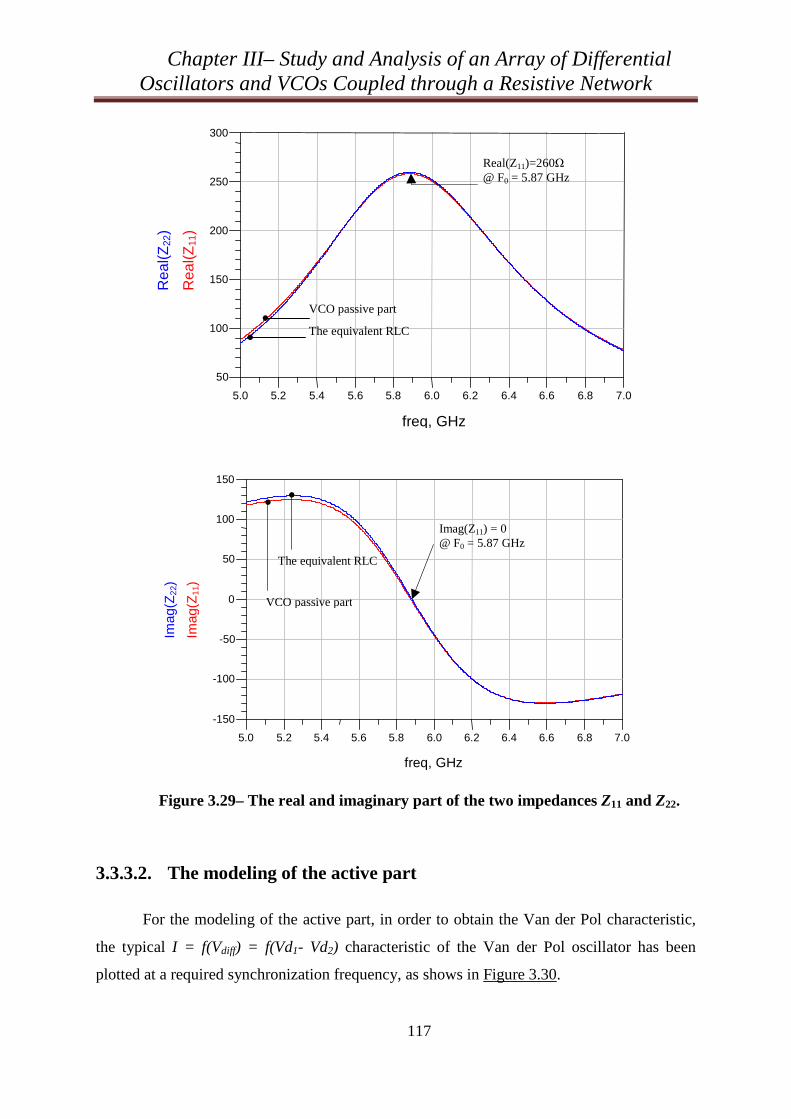
Chapter III– Study and Analysis of an Array of Differential Oscillators and VCOs Coupled through a Resistive Network
117
5.2 5.4 5.6 5.8 6.0 6.2 6.4 6.6 6.8 5.0 7.0
100
150
200
250
50
300
freq, GHz
Rea
l(Z11
)
Rea
l(Z22
) Real(Z11)=260 @ F0 = 5.87 GHz
VCO passive part
The equivalent RLC
5.2 5.4 5.6 5.8 6.0 6.2 6.4 6.6 6.8 5.0 7.0
-100
-50
0
50
100
-150
150
freq, GHz
Imag
(Z11
)
Imag
(Z22
)
Imag(Z11) = 0 @ F0 = 5.87 GHz
The equivalent RLC
VCO passive part
Figure 3.29– The real and imaginary part of the two impedances Z11 and Z22.
3.3.3.2. The modeling of the active part
For the modeling of the active part, in order to obtain the Van der Pol characteristic,
the typical I = f(Vdiff) = f(Vd1- Vd2) characteristic of the Van der Pol oscillator has been
plotted at a required synchronization frequency, as shows in Figure 3.30.
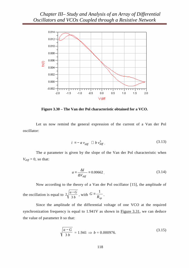
Chapter III– Study and Analysis of an Array of Differential Oscillators and VCOs Coupled through a Resistive Network
118
Figure 3.30 – The Van der Pol characteristic obtained for a VCO.
Let us now remind the general expression of the current of a Van der Pol
oscillator:
3diffdiff b v a vi +−= . (3.13)
The a parameter is given by the slope of the Van der Pol characteristic when
Vdiff = 0, so that:
006620.V
Ia
diff
=∆
∆= . (3.14)
Now according to the theory of a Van der Pol oscillator [15], the amplitude of
the oscillation is equal to b
Ga
32
−, with
vpRG
1= .
Since the amplitude of the differential voltage of one VCO at the required
synchronization frequency is equal to 1.941V as shown in Figure 3.31, we can deduce
the value of parameter b so that:
b
Ga
3
− = 1.941 ⇒ b = 0.000976.
(3.15)
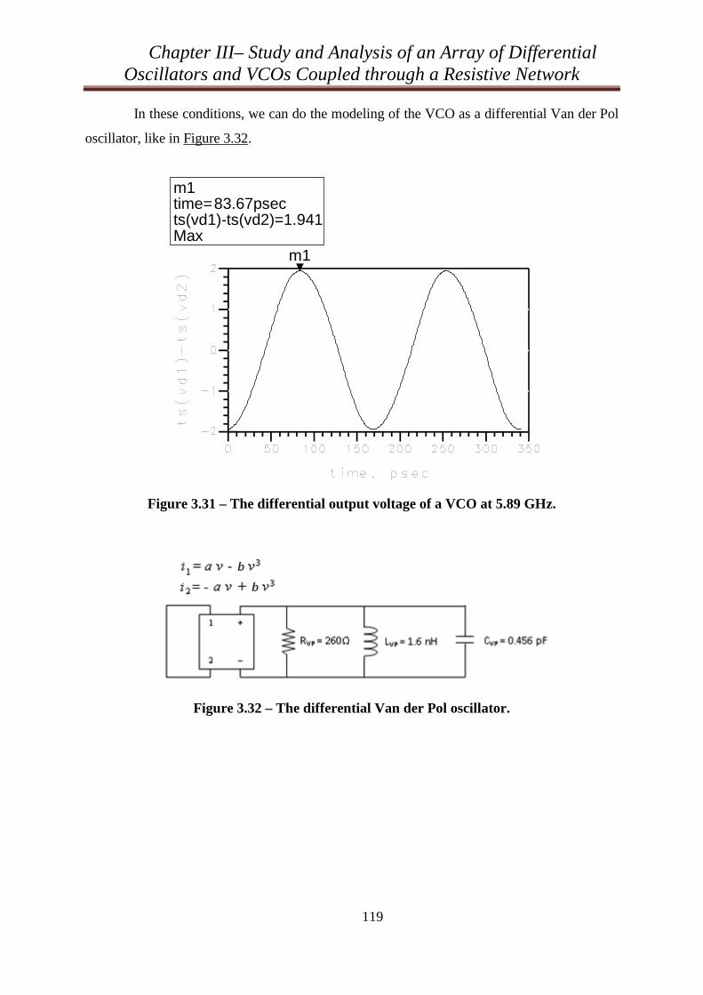
Chapter III– Study and Analysis of an Array of Differential Oscillators and VCOs Coupled through a Resistive Network
119
In these conditions, we can do the modeling of the VCO as a differential Van der Pol
oscillator, like in Figure 3.32.
m1
m1 time= ts(vd1)-ts(vd2)=1.941 Max
83.67psec
Figure 3.31 – The differential output voltage of a VCO at 5.89 GHz.
Figure 3.32 – The differential Van der Pol oscillator.
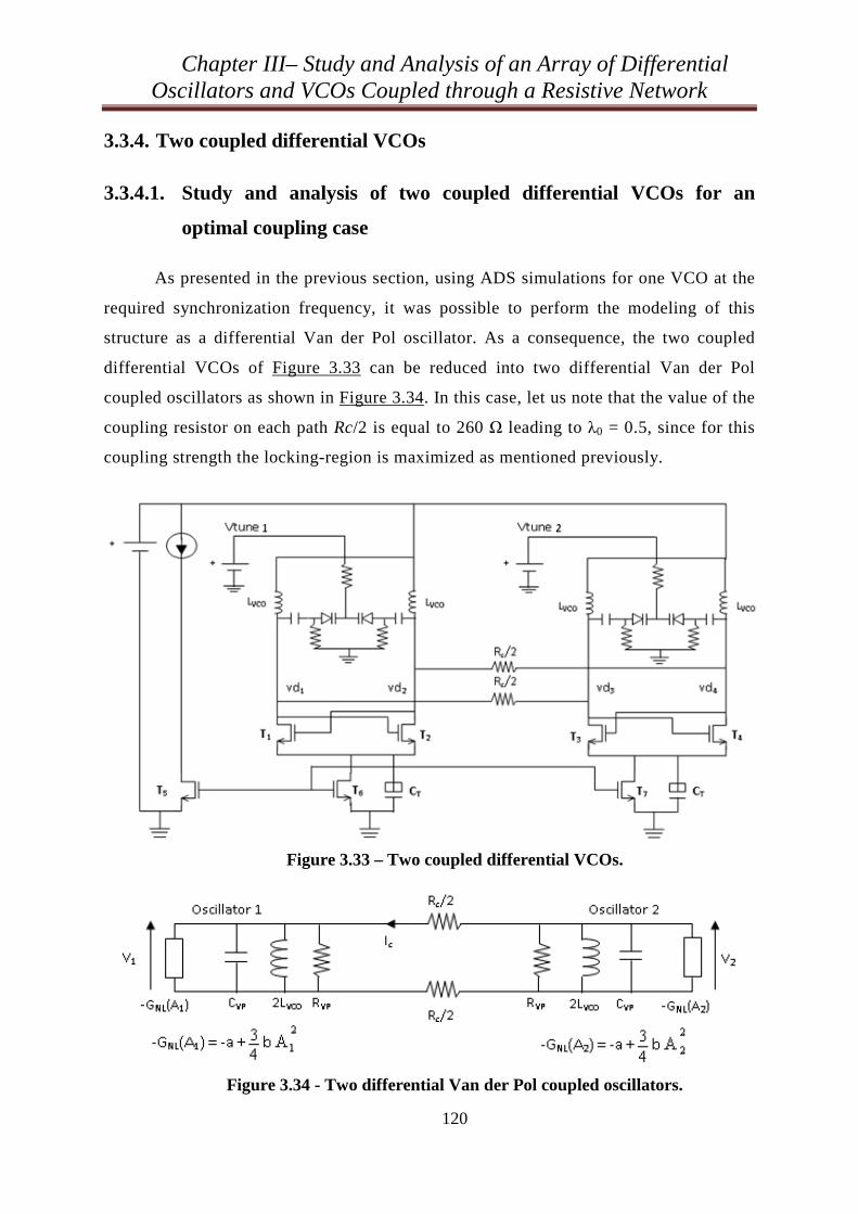
Chapter III– Study and Analysis of an Array of Differential Oscillators and VCOs Coupled through a Resistive Network
120
3.3.4. Two coupled differential VCOs
3.3.4.1. Study and analysis of two coupled differential VCOs for an
optimal coupling case
As presented in the previous section, using ADS simulations for one VCO at the
required synchronization frequency, it was possible to perform the modeling of this
structure as a differential Van der Pol oscillator. As a consequence, the two coupled
differential VCOs of Figure 3.33 can be reduced into two differential Van der Pol
coupled oscillators as shown in Figure 3.34. In this case, let us note that the value of the
coupling resistor on each path Rc/2 is equal to 260 leading to λ0 = 0.5, since for this
coupling strength the locking-region is maximized as mentioned previously.
Figure 3.33 – Two coupled differential VCOs.
Figure 3.34 - Two differential Van der Pol coupled oscillators.
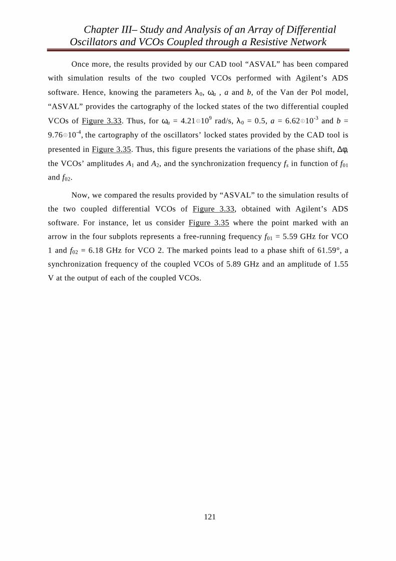
Chapter III– Study and Analysis of an Array of Differential Oscillators and VCOs Coupled through a Resistive Network
121
Once more, the results provided by our CAD tool “ASVAL” has been compared
with simulation results of the two coupled VCOs performed with Agilent’s ADS
software. Hence, knowing the parameters λ0, ωa , a and b, of the Van der Pol model,
“ASVAL” provides the cartography of the locked states of the two differential coupled
VCOs of Figure 3.33. Thus, for ωa = 4.21 109 rad/s, λ0 = 0.5, a = 6.62 10-3 and b =
9.76 10-4, the cartography of the oscillators’ locked states provided by the CAD tool is
presented in Figure 3.35. Thus, this figure presents the variations of the phase shift, ∆φ,
the VCOs’ amplitudes A1 and A2, and the synchronization frequency fs in function of f01
and f02.
Now, we compared the results provided by “ASVAL” to the simulation results of
the two coupled differential VCOs of Figure 3.33, obtained with Agilent’s ADS
software. For instance, let us consider Figure 3.35 where the point marked with an
arrow in the four subplots represents a free-running frequency f01 = 5.59 GHz for VCO
1 and f02 = 6.18 GHz for VCO 2. The marked points lead to a phase shift of 61.59°, a
synchronization frequency of the coupled VCOs of 5.89 GHz and an amplitude of 1.55
V at the output of each of the coupled VCOs.
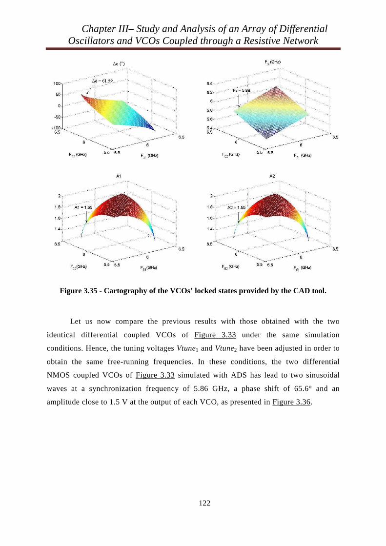
Chapter III– Study and Analysis of an Array of Differential Oscillators and VCOs Coupled through a Resistive Network
122
Figure 3.35 - Cartography of the VCOs’ locked states provided by the CAD tool.
Let us now compare the previous results with those obtained with the two
identical differential coupled VCOs of Figure 3.33 under the same simulation
conditions. Hence, the tuning voltages Vtune1 and Vtune2 have been adjusted in order to
obtain the same free-running frequencies. In these conditions, the two differential
NMOS coupled VCOs of Figure 3.33 simulated with ADS has lead to two sinusoidal
waves at a synchronization frequency of 5.86 GHz, a phase shift of 65.6° and an
amplitude close to 1.5 V at the output of each VCO, as presented in Figure 3.36.
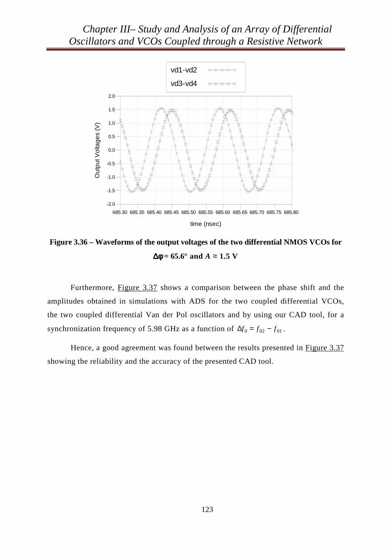
Chapter III– Study and Analysis of an Array of Differential Oscillators and VCOs Coupled through a Resistive Network
123
Figure 3.36 – Waveforms of the output voltages of the two differential NMOS VCOs for
∆∆∆∆φφφφ = 65.6° and A ≈ 1.5 V
Furthermore, Figure 3.37 shows a comparison between the phase shift and the
amplitudes obtained in simulations with ADS for the two coupled differential VCOs,
the two coupled differential Van der Pol oscillators and by using our CAD tool, for a
synchronization frequency of 5.98 GHz as a function of 01020 fff −=∆ .
Hence, a good agreement was found between the results presented in Figure 3.37
showing the reliability and the accuracy of the presented CAD tool.
685.35 685.40 685.45 685.50 685.55 685.60 685.65 685.70 685.75685.30 685.80
-1.5
-1.0
-0.5
0.0
0.5
1.0
1.5
-2.0
2.0
time (nsec)
Ou
tput
Vo
ltag
es
(V)
vd1-vd2
vd3-vd4
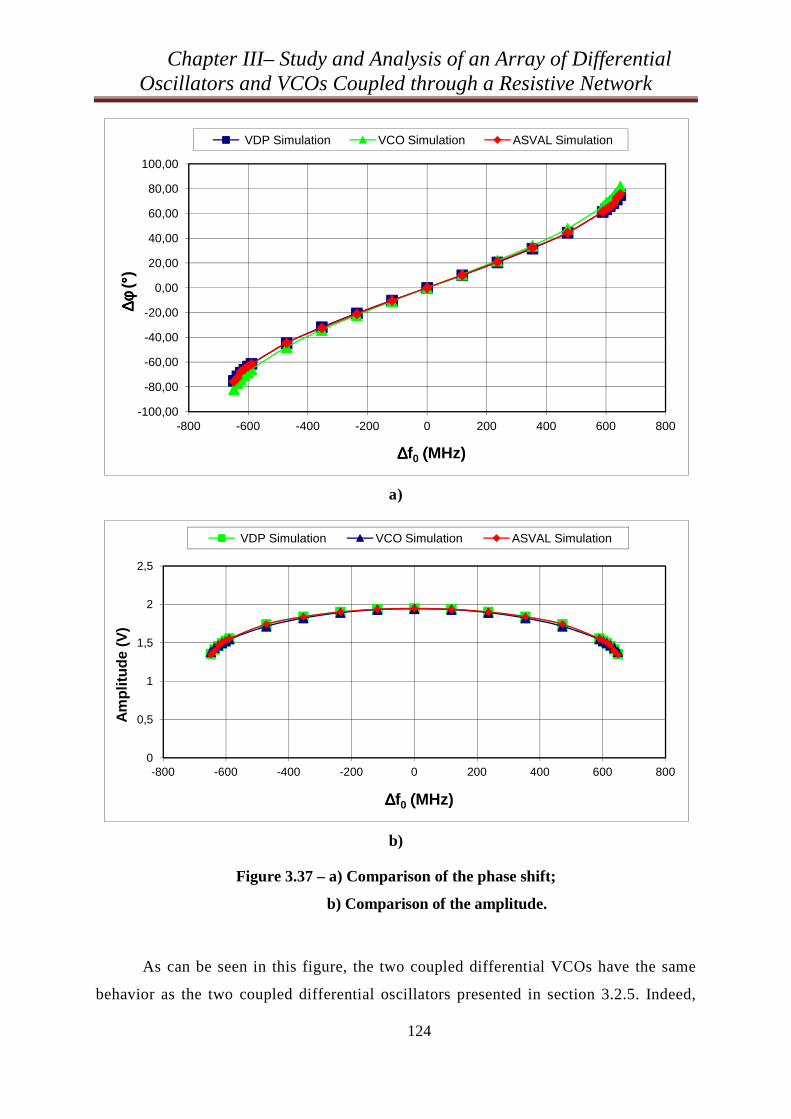
Chapter III– Study and Analysis of an Array of Differential Oscillators and VCOs Coupled through a Resistive Network
124
a)
b)
Figure 3.37 – a) Comparison of the phase shift;
b) Comparison of the amplitude.
As can be seen in this figure, the two coupled differential VCOs have the same
behavior as the two coupled differential oscillators presented in section 3.2.5. Indeed,
-100,00
-80,00
-60,00
-40,00
-20,00
0,00
20,00
40,00
60,00
80,00
100,00
-800 -600 -400 -200 0 200 400 600 800
∆φ∆φ ∆φ∆φ( °° °°
)
∆∆∆∆f0 ((((MHz)
VDP Simulation VCO Simulation ASVAL Simulation
0
0,5
1
1,5
2
2,5
-800 -600 -400 -200 0 200 400 600 800
Am
plit
ud
e (V
)
∆∆∆∆f0 ((((MHz)
VDP Simulation VCO Simulation ASVAL Simulation
Chapter III– Study and Analysis of an Array of Differential Oscillators and VCOs Coupled through a Resistive Network
125
one can notice that, as the oscillator tunings are moved apart, but the synchronization
frequency is halfway between, the phase shift increases until the locking-region
boundary is encountered. Furthermore, as shown in Figure 3.37.b, the amplitude is also
at a minimum at the locking-region boundaries and equal to the oscillators’ free-running
amplitude for equal tunings.
The main advantage of this CAD tool is that, in an extremely short simulation time,
all the phase shifts, synchronization frequencies and amplitudes of the differential coupled
system are computed, in function of the free-running frequencies f01 and f02 of the two
differential VCOs. Hence, since the inter-stage phase shift is independent of the number of
oscillators in the array, the proposed tool can also help the designer to find rapidly the free-
running frequencies of the two outermost VCOs of the array required to achieve the desired
phase shift. Indeed, without such a tool, a transient analysis of the VCO array for different
couples of VCOs’ free-running frequencies must be performed in order to find the phase shift
required for the targeted application.
As mentioned above, the previous simulations were performed for a coupling
constant λ0 = 0.5 for which the value of the coupling resistor Rc must be chosen equal to
520 Ω since the value of the parallel resistor Rvp of the resonator is equal to 260 Ω.
Hence, as for the case of two coupled differential oscillators presented in section 3.2.6,
it seems interesting to study again the behavior of the system in both weak and strong
coupling cases i.e. for values of λ0 respectively less and greater than 0.5. Furthermore,
a new analysis based on state equations method is presented in the next section.
3.3.4.1.1. Study and analysis of two coupled differential VCOs using the
state equation approach
In this section, we will study the behavior of the two coupled differential VCOs
presented previously, using the state equations method implemented in Matlab software.
In order to formulate the state equations in symbolic normal-form for nonlinear
time- invariant analog circuits, a computer program called SYSEG – Symbolic State
Equation Generation, developed by the Electrical Engineering Department of the
University Politehnica of Bucharest was used [50]. The program allows the analysis of
circuits containing both linear and nonlinear resistors, inductors and capacitors,
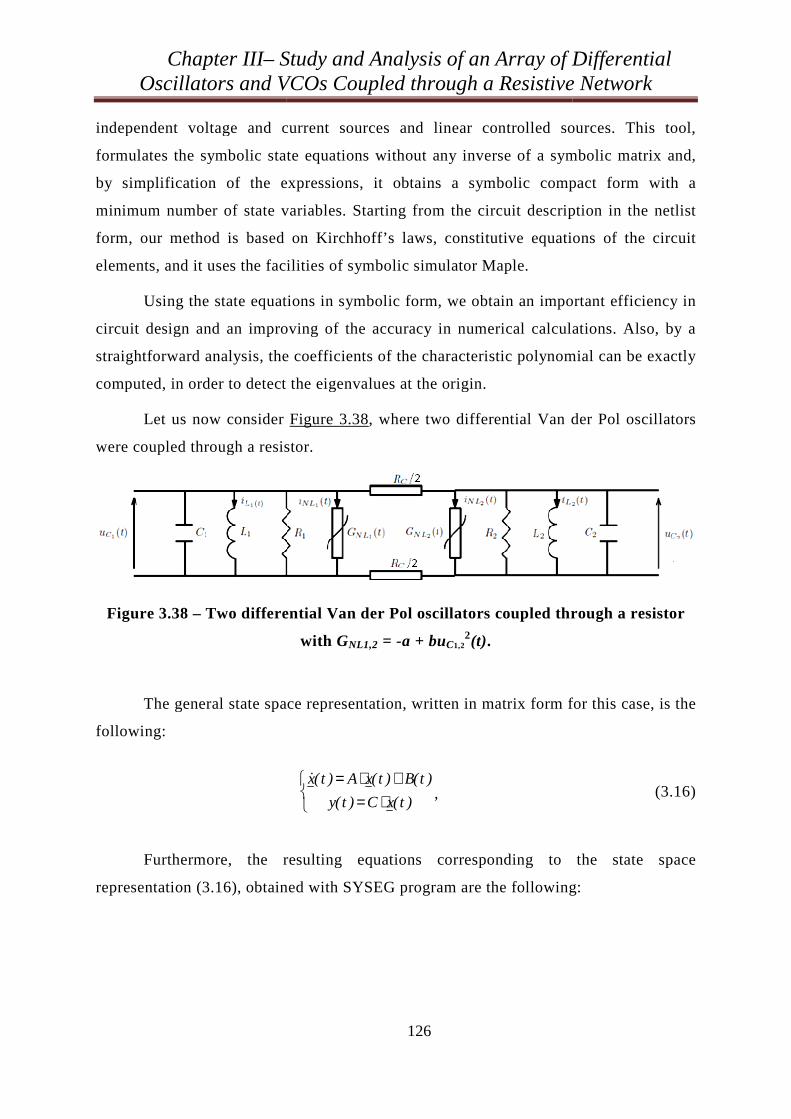
Chapter III– SOscillators and VC
independent voltage and c
formulates the symbolic stat
by simplification of the ex
minimum number of state v
form, our method is based
elements, and it uses the faci
Using the state equati
circuit design and an improv
straightforward analysis, the
computed, in order to detect
Let us now consider
were coupled through a resis
Figure 3.38 – Two differe
The general state spac
following:
Furthermore, the re
representation (3.16), obtaine
Study and Analysis of an Array of D VCOs Coupled through a Resistive
126
current sources and linear controlled so
tate equations without any inverse of a sym
expressions, it obtains a symbolic comp
variables. Starting from the circuit descrip
d on Kirchhoff’s laws, constitutive equatio
acilities of symbolic simulator Maple.
ations in symbolic form, we obtain an impor
roving of the accuracy in numerical calcula
he coefficients of the characteristic polynom
ct the eigenvalues at the origin.
er Figure 3.38, where two differential Van d
sistor.
rential Van der Pol oscillators coupled thr
with GNL1,2 = -a + buC1,22(t).
pace representation, written in matrix form fo
⋅=+⋅=
)t(xC)t(y
)t(B)t(xA)t(x,
resulting equations corresponding to
ined with SYSEG program are the following
of Differential ive Network
sources. This tool,
ymbolic matrix and,
mpact form with a
ription in the netlist
tions of the circuit
portant efficiency in
ulations. Also, by a
mial can be exactly
n der Pol oscillators
through a resistor
for this case, is the
(3.16)
the state space
ng:
Chapter III– Study and Analysis of an Array of Differential Oscillators and VCOs Coupled through a Resistive Network
127
)t(uLdt
)t(di
)t(uLdt
)t(di
iC
uC
bu
RCu
RRa
Cdt
)t(du
iC
uC
bu
RCu
RRa
Cdt
)t(du
CL
CL
LCCc
Cc
C
LCCc
Cc
C
!
2
2
1
1
2212
2
121
1
2
1
2
3
2222
1
3
1111
1
1
11111
11111
=
=
−−+
−−=
−−+
−−=
, (3.17)
These equations describes the system of the coupled oscillators as a set of inputs,
outputs and state variables related by first order differential equations. This modeling
method, using simple matrix operations can be applied for systems with multiple inputs
and multiple outputs (MIMO) and includes the effect of initial conditions [51].
Nevertheless, the most important advantage of this modeling form is that the
representation consists in simple first order differential equations and provides directly
a time domain solution, without adding unnecessary complexity and, also, it is more
adapted to computations and can incorporate nonlinear effects.
The state vector, noted x, composed of state variables, is a minimum set of
variables that are fully describing the system and its response to any given set of inputs.
These variables are related to energy storage elements in a circuit. For two coupled
differential Van der Pol oscillators, the state vector includes four variables, the currents
through the inductors )t(i L1 and )t(iL2
and the voltages across the capacitors )t(uC1 and
)t(uC2, as follows:
=
)t(i
)t(i
)t(u
)t(u
)t(x
L
L
C
C
2
1
2
1
, (3.18)
The state space matrices that describe the evolution of this system and
completely characterized its dynamic behavior are the following:
Chapter III– Study and Analysis of an Array of Differential Oscillators and VCOs Coupled through a Resistive Network
128
−⋅
−−
−⋅
−−
=
001
0
0001
10
1111
011111
1
1
1122
1111
L
L
CCRRa
CR
CCRCRRa
A cc
cc
,
⋅−
⋅−
=
0
0
3
2
3
1
2
1
)t(uC
b
)t(uC
b
)t(B C
C
(3.19)
and [ ]0011=C .
Now, in order to analyze the system of two coupled oscillators, the state
equations are implemented on Matlab Mathworks software and solved using the 4th
order Runge-Kutta method. This numerical technique is used to solve ordinary
differential equations. The implicit 4th order Runge-Kutta method has the following
form:
443322111 kwkwkwkwyy ii ++++=+ , (3.20)
where w1,… are the weights, and k1,... are h times various approximations to the
slopes at points in the step, and are given by:
),kbkbkby,hax(hfk
),kbkby,hax(hfk
),kby,hax(hfk
),y,x(hfk
ii
ii
ii
ii
36251434
231223
1112
1
++++=+++=
++==
(3.21)
where the a1,… and b1,… are constants to be determined.
Nevertheless, using this numerical method, the global error is of the same order
as the local error and the derivatives of the function are useless in the computation. One
of the most important advantage is that the “Automatic Error Control” can be made
easily.
Now, after solving the state equations system, in Figure 3.39 are presented the
resulting waveforms of the output voltages obtained for Rc/2 = 260 , a = 6.62 10-3 and
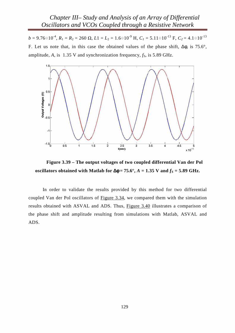
Chapter III– Study and Analysis of an Array of Differential Oscillators and VCOs Coupled through a Resistive Network
129
b = 9.76 10-4, R1 = R2 = 260 , L1 = L2 = 1.6 10-9 H, C1 = 5.11 10-13 F, C2 = 4.1 10-13
F. Let us note that, in this case the obtained values of the phase shift, ∆φ, is 75.6°,
amplitude, A, is 1.35 V and synchronization frequency, fS, is 5.89 GHz.
Figure 3.39 – The output voltages of two coupled differential Van der Pol
oscillators obtained with Matlab for ∆∆∆∆φφφφ = 75.6°, A = 1.35 V and fS = 5.89 GHz.
In order to validate the results provided by this method for two differential
coupled Van der Pol oscillators of Figure 3.34, we compared them with the simulation
results obtained with ASVAL and ADS. Thus, Figure 3.40 illustrates a comparison of
the phase shift and amplitude resulting from simulations with Matlab, ASVAL and
ADS.
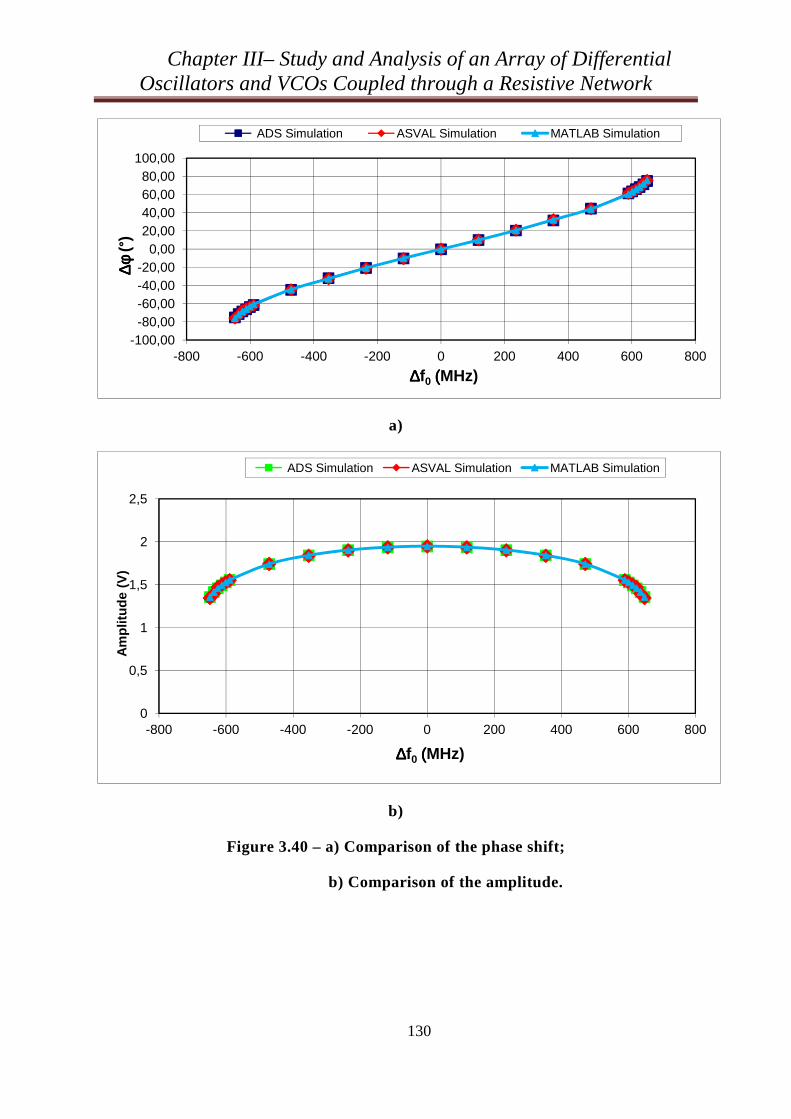
Chapter III– Study and Analysis of an Array of Differential Oscillators and VCOs Coupled through a Resistive Network
130
a)
b)
Figure 3.40 – a) Comparison of the phase shift;
b) Comparison of the amplitude.
-100,00-80,00-60,00-40,00-20,00
0,0020,0040,0060,0080,00
100,00
-800 -600 -400 -200 0 200 400 600 800
∆φ∆φ ∆φ∆φ(°
)
∆∆∆∆f0 ((((MHz)
ADS Simulation ASVAL Simulation MATLAB Simulation
0
0,5
1
1,5
2
2,5
-800 -600 -400 -200 0 200 400 600 800
Am
plit
ud
e (V
)
∆∆∆∆f0 ((((MHz)
ADS Simulation ASVAL Simulation MATLAB Simulation
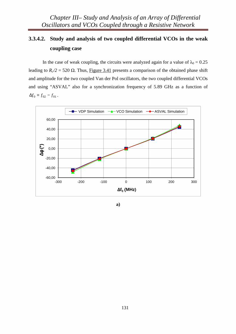
Chapter III– Study and Analysis of an Array of Differential Oscillators and VCOs Coupled through a Resistive Network
131
3.3.4.2. Study and analysis of two coupled differential VCOs in the weak
coupling case
In the case of weak coupling, the circuits were analyzed again for a value of λ0 = 0.25
leading to Rc/2 = 520 . Thus, Figure 3.41 presents a comparison of the obtained phase shift
and amplitude for the two coupled Van der Pol oscillators, the two coupled differential VCOs
and using “ASVAL” also for a synchronization frequency of 5.89 GHz as a function of
01020 fff −=∆ .
a)
-60,00
-40,00
-20,00
0,00
20,00
40,00
60,00
-300 -200 -100 0 100 200 300
∆φ∆φ ∆φ∆φ( °° °°
)
∆∆∆∆f0 ((((MHz)
VDP Simulation VCO Simulation ASVAL Simulation
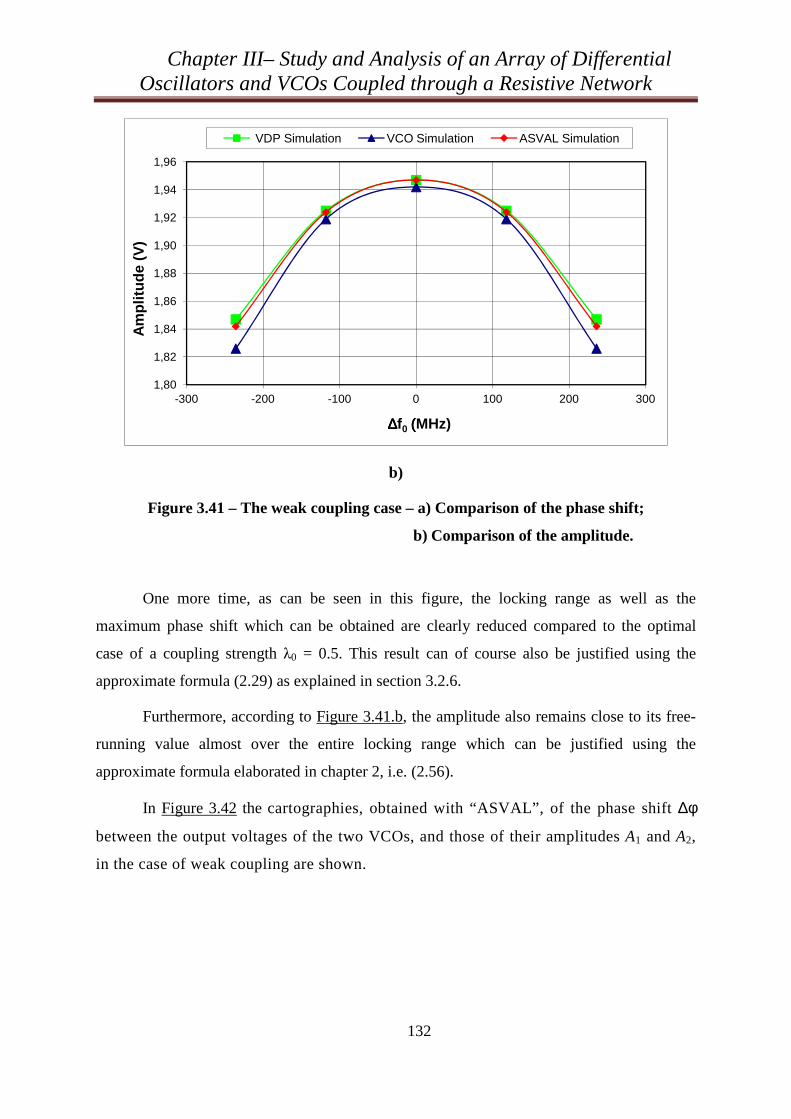
Chapter III– Study and Analysis of an Array of Differential Oscillators and VCOs Coupled through a Resistive Network
132
b)
Figure 3.41 – The weak coupling case – a) Comparison of the phase shift;
b) Comparison of the amplitude.
One more time, as can be seen in this figure, the locking range as well as the
maximum phase shift which can be obtained are clearly reduced compared to the optimal
case of a coupling strength λ0 = 0.5. This result can of course also be justified using the
approximate formula (2.29) as explained in section 3.2.6.
Furthermore, according to Figure 3.41.b, the amplitude also remains close to its free-
running value almost over the entire locking range which can be justified using the
approximate formula elaborated in chapter 2, i.e. (2.56).
In Figure 3.42 the cartographies, obtained with “ASVAL”, of the phase shift ∆φ
between the output voltages of the two VCOs, and those of their amplitudes A1 and A2,
in the case of weak coupling are shown.
1,80
1,82
1,84
1,86
1,88
1,90
1,92
1,94
1,96
-300 -200 -100 0 100 200 300
Am
plit
ud
e (V
)
∆∆∆∆f0 ((((MHz)
VDP Simulation VCO Simulation ASVAL Simulation
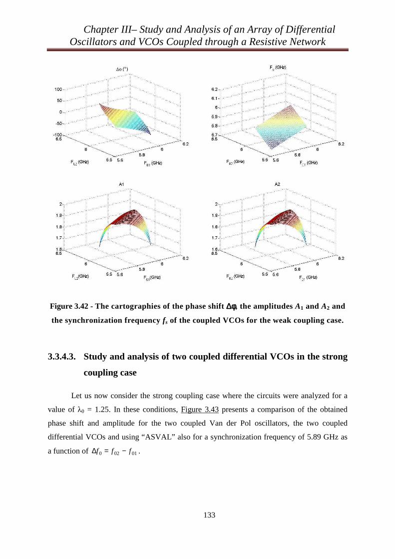
Chapter III– Study and Analysis of an Array of Differential Oscillators and VCOs Coupled through a Resistive Network
133
Figure 3.42 - The cartographies of the phase shift ∆∆∆∆φφφφ, the amplitudes A1 and A2 and
the synchronization frequency fs of the coupled VCOs for the weak coupling case.
3.3.4.3. Study and analysis of two coupled differential VCOs in the strong
coupling case
Let us now consider the strong coupling case where the circuits were analyzed for a
value of λ0 = 1.25. In these conditions, Figure 3.43 presents a comparison of the obtained
phase shift and amplitude for the two coupled Van der Pol oscillators, the two coupled
differential VCOs and using “ASVAL” also for a synchronization frequency of 5.89 GHz as
a function of 01020 fff −=∆ .
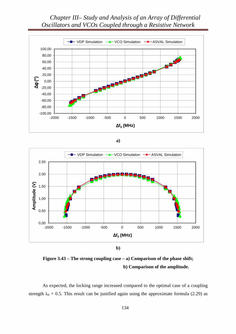
Chapter III– Study and Analysis of an Array of Differential Oscillators and VCOs Coupled through a Resistive Network
134
a)
b)
Figure 3.43 – The strong coupling case – a) Comparison of the phase shift;
b) Comparison of the amplitude.
As expected, the locking range increased compared to the optimal case of a coupling
strength λ0 = 0.5. This result can be justified again using the approximate formula (2.29) as
-100,00
-80,00
-60,00
-40,00
-20,00
0,00
20,00
40,00
60,00
80,00
100,00
-2000 -1500 -1000 -500 0 500 1000 1500 2000
∆φ∆φ ∆φ∆φ( °° °°
)
∆∆∆∆f0 ((((MHz)
VDP Simulation VCO Simulation ASVAL Simulation
0,00
0,50
1,00
1,50
2,00
2,50
-2000 -1500 -1000 -500 0 500 1000 1500 2000
Am
plit
ud
e (V
)
∆∆∆∆f0 ((((MHz)
VDP Simulation VCO Simulation ASVAL Simulation
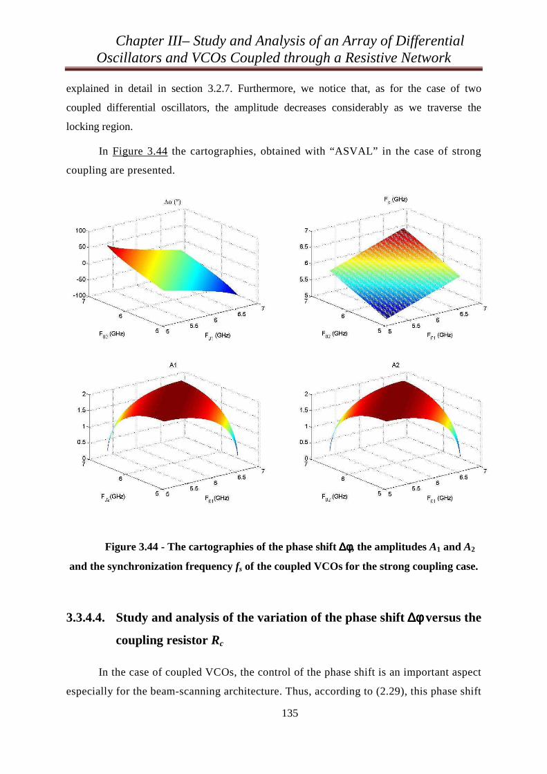
Chapter III– Study and Analysis of an Array of Differential Oscillators and VCOs Coupled through a Resistive Network
135
explained in detail in section 3.2.7. Furthermore, we notice that, as for the case of two
coupled differential oscillators, the amplitude decreases considerably as we traverse the
locking region.
In Figure 3.44 the cartographies, obtained with “ASVAL” in the case of strong
coupling are presented.
Figure 3.44 - The cartographies of the phase shift ∆∆∆∆φφφφ, the amplitudes A1 and A2
and the synchronization frequency fs of the coupled VCOs for the strong coupling case.
3.3.4.4. Study and analysis of the variation of the phase shift ∆∆∆∆φφφφ versus the
coupling resistor Rc
In the case of coupled VCOs, the control of the phase shift is an important aspect
especially for the beam-scanning architecture. Thus, according to (2.29), this phase shift
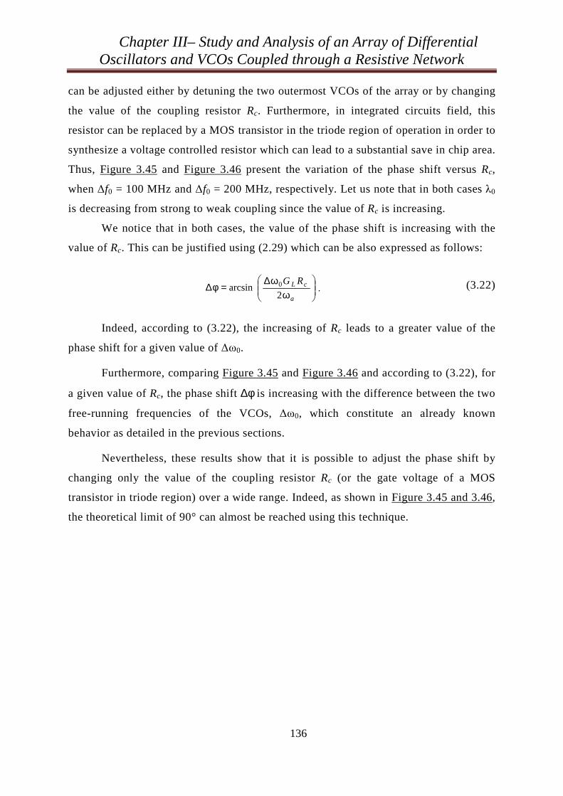
Chapter III– Study and Analysis of an Array of Differential Oscillators and VCOs Coupled through a Resistive Network
136
can be adjusted either by detuning the two outermost VCOs of the array or by changing
the value of the coupling resistor Rc. Furthermore, in integrated circuits field, this
resistor can be replaced by a MOS transistor in the triode region of operation in order to
synthesize a voltage controlled resistor which can lead to a substantial save in chip area.
Thus, Figure 3.45 and Figure 3.46 present the variation of the phase shift versus Rc,
when f0 = 100 MHz and f0 = 200 MHz, respectively. Let us note that in both cases λ0
is decreasing from strong to weak coupling since the value of Rc is increasing.
We notice that in both cases, the value of the phase shift is increasing with the
value of Rc. This can be justified using (2.29) which can be also expressed as follows:
ωω∆
=φ∆a
cL RG
2arcsin 0 . (3.22)
Indeed, according to (3.22), the increasing of Rc leads to a greater value of the
phase shift for a given value of ω0.
Furthermore, comparing Figure 3.45 and Figure 3.46 and according to (3.22), for
a given value of Rc, the phase shift ∆φ is increasing with the difference between the two
free-running frequencies of the VCOs, ω0, which constitute an already known
behavior as detailed in the previous sections.
Nevertheless, these results show that it is possible to adjust the phase shift by
changing only the value of the coupling resistor Rc (or the gate voltage of a MOS
transistor in triode region) over a wide range. Indeed, as shown in Figure 3.45 and 3.46,
the theoretical limit of 90° can almost be reached using this technique.
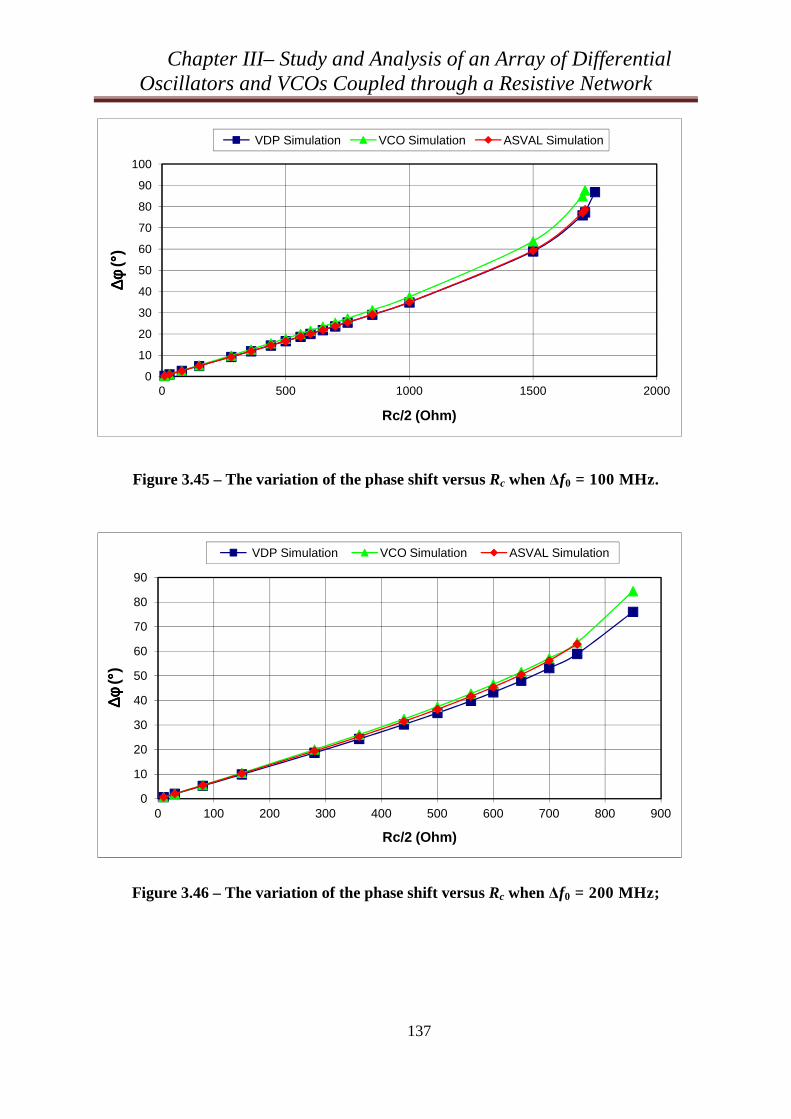
Chapter III– Study and Analysis of an Array of Differential Oscillators and VCOs Coupled through a Resistive Network
137
Figure 3.45 – The variation of the phase shift versus Rc when f0 = 100 MHz.
Figure 3.46 – The variation of the phase shift versus Rc when f0 = 200 MHz;
0
10
20
30
40
50
60
70
80
90
100
0 500 1000 1500 2000
∆φ∆φ ∆φ∆φ( °° °°
)
Rc/2 (Ohm)
VDP Simulation VCO Simulation ASVAL Simulation
0
10
20
30
40
50
60
70
80
90
0 100 200 300 400 500 600 700 800 900
∆φ∆φ ∆φ∆φ( °° °°
)
Rc/2 (Ohm)
VDP Simulation VCO Simulation ASVAL Simulation
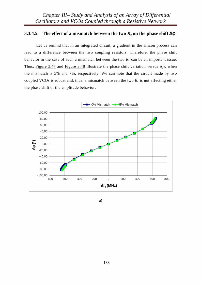
Chapter III– Study and Analysis of an Array of Differential Oscillators and VCOs Coupled through a Resistive Network
138
3.3.4.5. The effect of a mismatch between the two Rc on the phase shift ∆∆∆∆φφφφ
Let us remind that in an integrated circuit, a gradient in the silicon process can
lead to a difference between the two coupling resistors. Therefore, the phase shift
behavior in the case of such a mismatch between the two Rc can be an important issue.
Thus, Figure 3.47 and Figure 3.48 illustrate the phase shift variation versus f0, when
the mismatch is 5% and 7%, respectively. We can note that the circuit made by two
coupled VCOs is robust and, thus, a mismatch between the two Rc is not affecting either
the phase shift or the amplitude behavior.
a)
-100,00
-80,00
-60,00
-40,00
-20,00
0,00
20,00
40,00
60,00
80,00
100,00
-800 -600 -400 -200 0 200 400 600 800
∆φ∆φ ∆φ∆φ( °° °°
)
∆∆∆∆f0 ((((MHz)
0% Mismatch 5% Mismatch
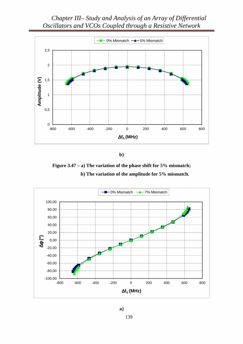
Chapter III– Study and Analysis of an Array of Differential Oscillators and VCOs Coupled through a Resistive Network
139
b)
Figure 3.47 – a) The variation of the phase shift for 5% mismatch;
b) The variation of the amplitude for 5% mismatch.
a)
0
0,5
1
1,5
2
2,5
-800 -600 -400 -200 0 200 400 600 800
Am
plit
ud
e (V
)
∆∆∆∆f0 ((((MHz)
0% Mismatch 5% Mismatch
-100,00
-80,00
-60,00
-40,00
-20,00
0,00
20,00
40,00
60,00
80,00
100,00
-800 -600 -400 -200 0 200 400 600 800
∆φ∆φ ∆φ∆φ( °° °°
)
∆∆∆∆f0 ((((MHz)
0% Mismatch 7% Mismatch
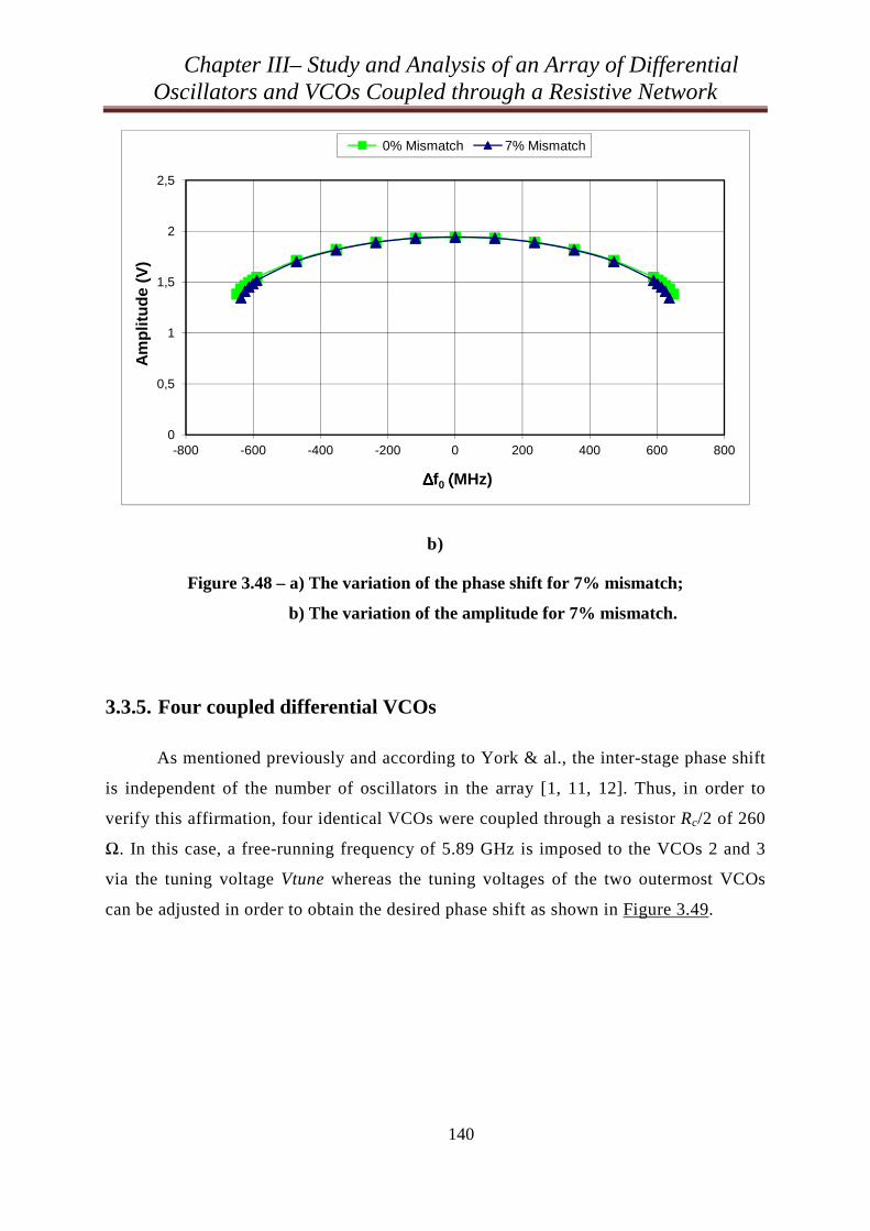
Chapter III– Study and Analysis of an Array of Differential Oscillators and VCOs Coupled through a Resistive Network
140
b)
Figure 3.48 – a) The variation of the phase shift for 7% mismatch;
b) The variation of the amplitude for 7% mismatch.
3.3.5. Four coupled differential VCOs
As mentioned previously and according to York & al., the inter-stage phase shift
is independent of the number of oscillators in the array [1, 11, 12]. Thus, in order to
verify this affirmation, four identical VCOs were coupled through a resistor Rc/2 of 260
Ω. In this case, a free-running frequency of 5.89 GHz is imposed to the VCOs 2 and 3
via the tuning voltage Vtune whereas the tuning voltages of the two outermost VCOs
can be adjusted in order to obtain the desired phase shift as shown in Figure 3.49.
0
0,5
1
1,5
2
2,5
-800 -600 -400 -200 0 200 400 600 800
Am
plit
ud
e (V
)
∆∆∆∆f0 ((((MHz)
0% Mismatch 7% Mismatch
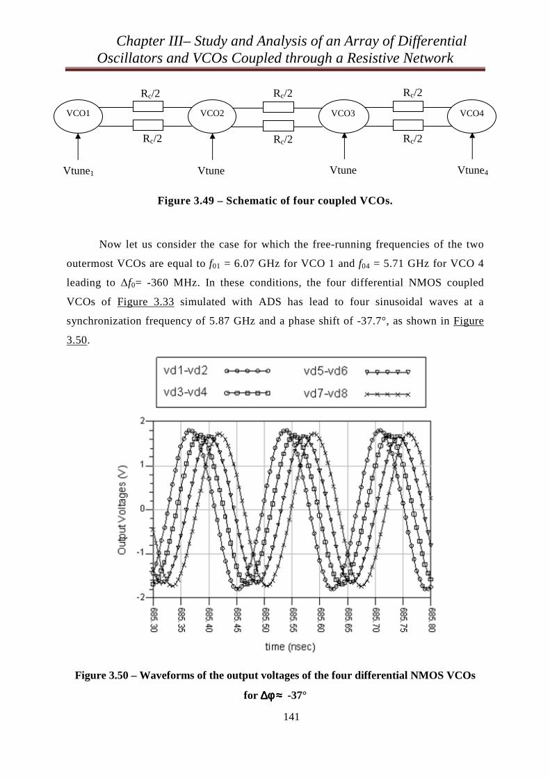
Chapter III– Study and Analysis of an Array of Differential Oscillators and VCOs Coupled through a Resistive Network
141
Figure 3.49 – Schematic of four coupled VCOs.
Now let us consider the case for which the free-running frequencies of the two
outermost VCOs are equal to f01 = 6.07 GHz for VCO 1 and f04 = 5.71 GHz for VCO 4
leading to f0= -360 MHz. In these conditions, the four differential NMOS coupled
VCOs of Figure 3.33 simulated with ADS has lead to four sinusoidal waves at a
synchronization frequency of 5.87 GHz and a phase shift of -37.7°, as shown in Figure
3.50.
Figure 3.50 – Waveforms of the output voltages of the four differential NMOS VCOs
for ∆∆∆∆φφφφ ≈≈≈≈ -37°
Rc/2 Rc/2
Rc/2 Rc/2
VCO1 VCO2
Rc/2
Rc/2
VCO3 VCO4
Vtune1 Vtune Vtune Vtune4
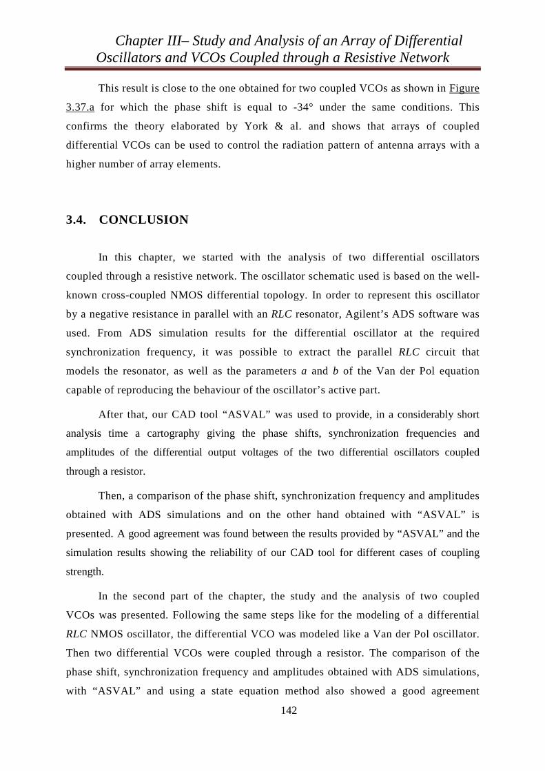
Chapter III– Study and Analysis of an Array of Differential Oscillators and VCOs Coupled through a Resistive Network
142
This result is close to the one obtained for two coupled VCOs as shown in Figure
3.37.a for which the phase shift is equal to -34° under the same conditions. This
confirms the theory elaborated by York & al. and shows that arrays of coupled
differential VCOs can be used to control the radiation pattern of antenna arrays with a
higher number of array elements.
3.4. CONCLUSION
In this chapter, we started with the analysis of two differential oscillators
coupled through a resistive network. The oscillator schematic used is based on the well-
known cross-coupled NMOS differential topology. In order to represent this oscillator
by a negative resistance in parallel with an RLC resonator, Agilent’s ADS software was
used. From ADS simulation results for the differential oscillator at the required
synchronization frequency, it was possible to extract the parallel RLC circuit that
models the resonator, as well as the parameters a and b of the Van der Pol equation
capable of reproducing the behaviour of the oscillator’s active part.
After that, our CAD tool “ASVAL” was used to provide, in a considerably short
analysis time a cartography giving the phase shifts, synchronization frequencies and
amplitudes of the differential output voltages of the two differential oscillators coupled
through a resistor.
Then, a comparison of the phase shift, synchronization frequency and amplitudes
obtained with ADS simulations and on the other hand obtained with “ASVAL” is
presented. A good agreement was found between the results provided by “ASVAL” and the
simulation results showing the reliability of our CAD tool for different cases of coupling
strength.
In the second part of the chapter, the study and the analysis of two coupled
VCOs was presented. Following the same steps like for the modeling of a differential
RLC NMOS oscillator, the differential VCO was modeled like a Van der Pol oscillator.
Then two differential VCOs were coupled through a resistor. The comparison of the
phase shift, synchronization frequency and amplitudes obtained with ADS simulations,
with “ASVAL” and using a state equation method also showed a good agreement
Chapter III– Study and Analysis of an Array of Differential Oscillators and VCOs Coupled through a Resistive Network
143
between the results showing the usefulness of our CAD tool for the design of an array of
differential VCOs coupled through a broadband network. Furthermore, the variation of the
phase shift versus the coupling resistor was also investigated showing that it is possible
to adjust the phase shift by changing only the value of the coupling resistor Rc over a
wide range. The robustness of the circuit regarding the mismatch between the two
coupling resistors was also presented.
Finally, four VCOs were coupled through a resistor showing that arrays of
coupled differential VCOs can be used to control the radiation pattern of antenna arrays
with a higher number of array elements.

144
FINAL CONCLUSION
Final Conclusion
145
Arrays of coupled oscillators are receiving increasing interest in both military and
commercial applications. They are used to achieve high-power RF sources through
coherent power combining. Another application is the beam steering of antenna arrays. The
radiation pattern of a phased antenna array is steered in a particular direction by
establishing a constant phase progression throughout the oscillator’s chain.
Nevertheless, it is shown that the theoretical limit of the phase shift that can be
obtained by slightly detuning the end elements of the array by equal amounts but in
opposite directions is only ±90°. In this context, it seemed interesting to study and analyze
the behavior of an array of coupled differential oscillators or Voltage Controlled
Oscillators (VCOs) since, in this case, the theoretical limit of the phase shift is within 360°
due to the differential operation of the array leading to a more efficient beam-scanning
architecture for example. As a consequence, the aim of this work was to study and analyze
the behavior of coupled differential oscillators and VCOs used to control antenna arrays.
This work was organized in 3 chapters, followed by references and appendixes.
Chapter I, Coupled-Oscillator Arrays - Application, reminds briefly the oscillators’
principle as well as their classifications and applications in the communication system. The
principle of an oscillator can be represented by a nonlinear impedance, which is the active
part of the oscillator, in parallel with the equivalent impedance of the resonator. The
condition for sustaining the oscillations can be fulfilled only if the real part of the non-
linear impedance is negative, which can be obtained by an active element. Oscillators are
classified in accordance with the wave shapes they produce and the circuitry required for
producing the desired oscillations.
In the second part of the chapter, a state of the art of coupled-oscillators theory was
presented followed by a few applications of antenna arrays. Due to their different
geometric configuration, antenna arrays can have an important role in controlling the
radiation angle of the pattern. Therefore, and also for simplicity reasons, a linear
configuration was presented in this section. The most important advantage of controlling
the antenna array consists in generating the amplitudes and/or the phases necessary for
orientating the radiation pattern in the desired direction. As a consequence, various
technical solutions were proposed, including the coupled oscillators approach.
Final Conclusion
146
Chapter II, Theoretical Analysis of Coupled Oscillators Applied to an Antenna
Array, presents in the first part a complete review of R. York’s theory, giving the dynamics
of two Van der Pol oscillators coupled through a series resonant network. Then, the case of
a resistive coupling circuit was deduced from this system of equations.
Then, showing the limitation of this approach regarding the prediction of the
oscillators’ amplitudes, a new formulation of the nonlinear equations describing the
oscillators’ locked states was proposed.
Nevertheless, due to the trigonometric and strongly non-linear aspect of this system
of nonlinear equations describing the locked states of two coupled Van der Pol oscillators,
mathematical manipulations were applied in order to obtain a new system easier to solve
numerically. Thus, a simpler system of three equations with three unknowns was obtained
allowing then to implement a CAD tool that permits to extract, in an extremely short
simulation time, a cartography giving the frequency locking region of two differential
oscillators coupled through a resistive network. This cartography can help the designer to
find rapidly the free-running frequencies of the two outermost oscillators or VCOs of the
array required to achieve the desired phase shift.
Chapter III, Study and Analysis of an Array of Differential Oscillators and VCOs
Coupled through a Resistive Network, begins with the analysis of two RLC NMOS
differential oscillators coupled through a resistive network. The oscillator schematic used
is based on the well-known cross-coupled NMOS differential topology, which provides the
negative resistance to compensate for the tank losses of the resonator. Since the theory
implemented in our CAD tool “ASVAL” uses Van der Pol oscillators to model microwave
coupled oscillators, a modeling procedure of the differential oscillator as a differential Van
der Pol oscillator was performed. To do so, Agilent’s ADS software was used. From ADS
simulation results for the differential oscillator at the required synchronization frequency, it
was possible to extract the parallel RLC circuit that models the resonator, as well as the
parameters a and b of the Van der Pol equation capable of reproducing the behaviour of the
oscillator’s active part.
After that, the proposed CAD tool was used to provide the cartography giving the
phase shifts, synchronization frequencies and amplitudes of the differential output voltages
Final Conclusion
147
of the two differential oscillators coupled through a resistor. Then, in order to validate
these results, a comparison to the simulation results of the two coupled differential
oscillators obtained with Agilent’s ADS software was presented. A good agreement was
found between the results provided by our CAD tool and the simulation results showing the
reliability of the presented tool for different cases of coupling strength
In the last part of the chapter, the same study was performed for the case of two
differential Voltage Controlled Oscillators (VCOs) coupled through a resistor. The
comparison of the phase shift, synchronization frequencies and amplitudes obtained with
ADS simulations, with “ASVAL” and using a state equation method also showed good
agreements between the results proving the usefulness of our CAD tool for the design of an
array of differential VCOs coupled through a broadband network. Furthermore, the study of the
variation of the phase shift versus the coupling resistor was also investigated as well as the
robustness of the circuit regarding the mismatch between the two coupling resistors.
Finally, four VCOs were coupled through a resistor showing that arrays of coupled
differential VCOs can be used to control the radiation pattern of antenna arrays with a
higher number of array elements.
PERSONAL CONTRIBUTIONS
• The study of generality on antenna arrays, uniform linear network and the
controlling of radiation angle of the pattern.
• The state of the art on generality and classification of oscillators.
• The study and the analysis of the dynamic equations of two oscillators coupled
through a RLC circuit.
• A nonlinear system of equations describing the oscillators’ locked states for the
specific case of a resistive coupling network was deduced.
• Showing the limitation of R. York approach regarding the prediction of the oscillators’
amplitudes, a new formulation of the nonlinear equations describing the oscillators’
locked states was developed.
Final Conclusion
148
• The specific dynamic equations of two oscillators coupled through a resistive network were
deduced.
• Because of the trigonometric and strongly non-linear aspect of the dynamic equations
describing the oscillators’ locked states, mathematical manipulations were applied in
order to obtain a new system easier to solve numerically.
• The elaboration of a CAD tool which provides, in a considerably short simulation time,
the frequency locking region of two coupled Van der Pol oscillators.
• The cartography of the synchronization area, phase shift and amplitudes of two
coupled oscillators using the CAD tool was generated.
• Simulations using Agilent Advanced Design System were performed for the analysis of
two coupled NMOS differential oscillators and two coupled differential Van der Pol
oscillators.
• The modeling procedure of two coupled NMOS differential oscillators as two coupled
differential Van der Pol oscillators, with a resistive coupling network was performed.
Good agreements between the simulations of the circuit, the model and the theoretical
results from our CAD tool were found.
• The analysis of the behavior of two coupled NMOS differential oscillators in the case
of strong and weak coupling was realized.
• The modeling procedure of two coupled differential VCOs as two coupled differential
Van der Pol oscillators, with a resistive coupling network was performed.
• The cartography of the synchronization area, phase shift and amplitudes of two
coupled differential VCOs using the CAD tool was generated.
• The study and analysis of an array of two differential VCOs coupled through a resistive
network was realized.
• The analysis and study of four differential VCOs coupled through a resistive network was
performed.

Final Conclusion
149
• Simulations using Matlab Mathworks software of an array of two differential Van der Pol
oscillators coupled through a resistor using the state space representation. Comparison of
the obtained results using the theory and Agilent Advanced Design System simulations.
FUTURE PROSPECTS
• The design of an array of coupled VCOs using a 0,25 µm BiCMOS SiGe process.
• The elaboration of a modeling procedure of two single-ended oscillators, starting from
the state equation representation leading to the parameters identification of two coupled
Van der Pol oscillators. This approach is useful in the design of an array of coupled
oscillators allowing to determine the outermost free-running frequencies of the array.
List of Publications
150
Publications
Iulia Dumitrescu, Mihaela Ionita , Jean-Marie Paillot, Mihai Iordache, Couples theory des oscillateurs couples appliquée aux antennes réseaux, The Scientific Bulletin of Electrical Engineering Faculty, year 9, No 2, pp. 27-35, 2009; Iulia Dumitrescu, Mihai Iordache, Mihaela Ionita , Analysis of Coupled Oscillators through a Series RLC Network, Proceedings of the 10th International Conference on Development and Application Systems, Suceava, Romania, pp. 65, May 2010; Iulia Dumitrescu, Ileana Calomfirescu, Mihaela Ionita, Analiza Pspice a oscilatoarelor de tip Van der Pol cuplate, Simpozionul National de Electrotehnica Teoretica, Bucuresti, Romania, November 2009; Mihai Iordache, Jean-Marie Paillot, Iulia Dumitrescu, Mihaela Ionita , Analysis of coupled Oscillators Applied to Antenna Arrays, 10th International Conference on Applied and Theoretical Electricity, Craiova, Romania, pp. 25-29, October 2010; Mihaela Ionita , Iulia Dumitrescu, Mihai Iordache, Analysis of Coupled Oscillators by Semi-State Variable Method, U.P.B. Scientific Bulletin Series C – Electrical Engineering, no. 3, August 2012, (in press).
Publications in international data base
Mihai Iordache, Lucia Dumitriu, Iulia Dumitrescu, Mihaela Ionita , Analysis of Coupled Oscillators Applied to 1D Antenna Array, 5th European Conference on Circuits and Systems for Communications, Belgrade Serbia, pp. 256-260, November 2010; Mihaela Ionita , David Cordeau, Jean-Marie Paillot, Mihai Iordache, Analysis and Design of an Array of Two Differential Oscillators Coupled Through a Resistive Network, 20th European Conference on Circuit Theory and Design, Linkoping, Sweden, pp. 73-76, August 2011; Mihaela Ionita , David Cordeau, Jean-Marie Paillot, Smail Bachir, Mihai Iordache, A CAD Tool for an Array of Differential Oscillators Coupled Through a Broadband Network, International Journal of RF and Microwave Computer-aided Engineering, (in press); Mihaela Ionita , Mihai Iordache, Lucia Dumitriu, David Cordeau, Jean-Marie Paillot, Generation of the Coupling Circuit Parameters for the Coupled Oscillators Used in Antenna Arrays, International Conference on Synthesis, Modeling, Analysis and Simulation Methods and Applications to Circuit Design, (accepted for publication).

151
APPENDIX A
Appendix A – Marquardt Algorithm
152
Marquardt algorithm
In mathematics and computing, the Levenberg–Marquardt algorithm (LMA)
provides a numerical solution to the problem of minimizing a function, generally nonlinear,
over a space of parameters of the function. These minimization problems arise especially in
least squares curve fitting and nonlinear programming [46].
The LMA interpolates between the Gauss–Newton algorithm (GNA) and the method
of gradient descent. The LMA is more robust than the GNA, which means that in many
cases it finds a solution even if it starts very far off the final minimum. For well-behaved
functions and reasonable starting parameters, the LMA tends to be a bit slower than the
GNA. LMA can also be viewed as Gauss–Newton using a trust region approach.
The LMA is a very popular curve-fitting algorithm used in many software
applications for solving generic curve-fitting problems. However, the LMA finds only a
local minimum, not a global minimum.
Caveat Emptor
One important limitation that is very often over-looked is that it only optimizes for
residual errors in the dependant variable (y). It thereby implicitly assumes that any errors in
the independent variable are zero or at least ratio of the two is so small as to be negligible.
This is not a defect, it is intentional, but it must be taken into account when deciding
whether to use this technique to do a fit. While this may be suitable in context of a
controlled experiment there are many situations where this assumption cannot be made. In
such situations either non-least squares methods should be used or the least-squares fit
should be done in proportion to the relative errors in the two variables, not simply the
vertical "y" error. Failing to recognize this can lead to a fit which is significantly incorrect
and fundamentally wrong. It will usually underestimate the slope. This may or may not be
obvious to the eye.
Microsoft Excel's chart offers a trend fit that has this limitation that is
undocumented. Users often fall into this trap assuming the fit is correctly calculated for all
situations. OpenOffice spreadsheet copied this feature and presents the same problem.
Appendix A – Marquardt Algorithm
153
The problem
The primary application of the Levenberg–Marquardt algorithm is in the least squares curve
fitting problem: given a set of m empirical datum pairs of independent and dependent variables, (xi,
yi), optimize the parameters β of the model curve f(x,β) so that the sum of the squares of the
deviations:
∑=
β−=βm
iii )],x(fy[)(S
1
2,
becomes minimal.
The solution
Like other numeric minimization algorithms, the Levenberg–Marquardt algorithm is
an iterative procedure. To start a minimization, the user has to provide an initial guess for
the parameter vector, β. In cases with only one minimum, an uninformed standard guess
like βT=(1,1,...,1) will work fine; in cases with multiple minima, the algorithm converges
only if the initial guess is already somewhat close to the final solution.
In each iteration step, the parameter vector, β, is replaced by a new estimate, β + δ.
To determine δ, the functions ),x(f i δ+β are approximated by their linearization:
δ+β≈δ+β iii J),x(f),x(f ,
where
β∂β∂
=),x(f
J ii ,
is the gradient (row-vector in this case) of f with respect to β.
At its minimum, the sum of squares, S(β), the gradient of S with respect to δ will be
zero. The above first-order approximation of ),x(f i δ+β gives:
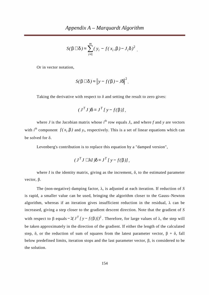
Appendix A – Marquardt Algorithm
154
∑=
δ−β−≈δ+βm
iiii )J),x(fy()(S
1
2.
Or in vector notation,
2δ−β−≈δ+β J)(fy)(S .
Taking the derivative with respect to δ and setting the result to zero gives:
)](fy[J)JJ( TT β−=δ ,
where J is the Jacobian matrix whose i th row equals Ji, and where f and y are vectors
with i th component ),x(f i β and yi, respectively. This is a set of linear equations which can
be solved for δ.
Levenberg's contribution is to replace this equation by a "damped version",
)](fy[J)IJJ( TT β−=δλ+ ,
where I is the identity matrix, giving as the increment, δ, to the estimated parameter
vector, β.
The (non-negative) damping factor, λ, is adjusted at each iteration. If reduction of S
is rapid, a smaller value can be used, bringing the algorithm closer to the Gauss–Newton
algorithm, whereas if an iteration gives insufficient reduction in the residual, λ can be
increased, giving a step closer to the gradient descent direction. Note that the gradient of S
with respect to β equals 22 )])(fy[J( T β−− . Therefore, for large values of λ, the step will
be taken approximately in the direction of the gradient. If either the length of the calculated
step, δ, or the reduction of sum of squares from the latest parameter vector, β + δ, fall
below predefined limits, iteration stops and the last parameter vector, β, is considered to be
the solution.
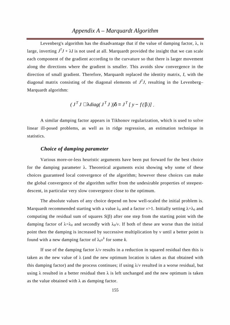
Appendix A – Marquardt Algorithm
155
Levenberg's algorithm has the disadvantage that if the value of damping factor, λ, is
large, inverting JTJ + λI is not used at all. Marquardt provided the insight that we can scale
each component of the gradient according to the curvature so that there is larger movement
along the directions where the gradient is smaller. This avoids slow convergence in the
direction of small gradient. Therefore, Marquardt replaced the identity matrix, I, with the
diagonal matrix consisting of the diagonal elements of JTJ, resulting in the Levenberg–
Marquardt algorithm:
)](fy[J))JJ(diagJJ( TTT β−=δλ+ .
A similar damping factor appears in Tikhonov regularization, which is used to solve
linear ill-posed problems, as well as in ridge regression, an estimation technique in
statistics.
Choice of damping parameter
Various more-or-less heuristic arguments have been put forward for the best choice
for the damping parameter λ. Theoretical arguments exist showing why some of these
choices guaranteed local convergence of the algorithm; however these choices can make
the global convergence of the algorithm suffer from the undesirable properties of steepest-
descent, in particular very slow convergence close to the optimum.
The absolute values of any choice depend on how well-scaled the initial problem is.
Marquardt recommended starting with a value λ0 and a factor ν>1. Initially setting λ=λ0 and
computing the residual sum of squares S(β) after one step from the starting point with the
damping factor of λ=λ0 and secondly with λ0/ν. If both of these are worse than the initial
point then the damping is increased by successive multiplication by ν until a better point is
found with a new damping factor of λ0νk for some k.
If use of the damping factor λ/ν results in a reduction in squared residual then this is
taken as the new value of λ (and the new optimum location is taken as that obtained with
this damping factor) and the process continues; if using λ/ν resulted in a worse residual, but
using λ resulted in a better residual then λ is left unchanged and the new optimum is taken
as the value obtained with λ as damping factor.

156
APPENDIX B
Appendix B – Intelligent Transport Systems
157
Intelligent Transport Systems
The term Intelligent Transport Systems (ITS) refers to information and
communication technology (applied to transport infrastructure and vehicles) that improve
transport outcomes such as transport safety, transport productivity, travel reliability,
informed travel choices, social equity, environmental performance and network operation
resilience [49].
Background
Interest in ITS comes from the problems caused by traffic congestion and a synergy
of new information technology for simulation, real-time control, and communications
networks. Traffic congestion has been increasing worldwide as a result of increased
motorization, urbanization, population growth, and changes in population density.
Congestion reduces efficiency of transportation infrastructure and increases travel time, air
pollution, and fuel consumption.
The United States, for example, saw large increases in both motorization and
urbanization starting in the 1920s that led to migration of the population from the sparsely
populated rural areas and the densely packed urban areas into suburbs. The industrial
economy replaced the agricultural economy, leading the population to move from rural
locations into urban centers. At the same time, motorization was causing cities to expand
because motorized transportation could not support the population density that the existing
mass transit systems could. Suburbs provided a reasonable compromise between population
density and access to a wide variety of employment, goods, and services that were
available in the more densely populated urban centers. Further, suburban infrastructure
could be built quickly, supporting a rapid transition from a rural/agricultural economy to an
industrial/urban economy.
Recent governmental activity in the area of ITS – specifically in the United States –
is further motivated by an increasing focus on homeland security. Many of the proposed
ITS systems also involve surveillance of the roadways, which is a priority of homeland
security. Funding of many systems comes either directly through homeland security
Appendix B – Intelligent Transport Systems
158
organizations or with their approval. Further, ITS can play a role in the rapid mass
evacuation of people in urban centers after large casualty events such as a result of a
natural disaster or threat. Much of the infrastructure and planning involved with ITS
parallels the need for homeland security systems.
In the developing world, the migration of people from rural to urbanized habitats
has progressed differently. Many areas of the developing world have urbanized without
significant motorization and the formation of suburbs. In areas like Santiago, Chile, a high
population density is supported by a multimodal system of walking, bicycle transportation,
motorcycles, buses, and trains. A small portion of the population can afford automobiles,
but the automobiles greatly increase the congestion in these multimodal transportation
systems. They also produce a considerable amount of air pollution, pose a significant safety
risk, and exacerbate feelings of inequities in the society.
Other parts of the developing world, such as China, remain largely rural but are
rapidly urbanizing and industrializing. In these areas a motorized infrastructure is being
developed alongside motorization of the population. Great disparity of wealth means that
only a fraction of the population can motorize, and therefore the highly dense multimodal
transportation system for the poor is cross-cut by the highly motorized transportation
system for the rich. The urban infrastructure is being rapidly developed, providing an
opportunity to build new systems that incorporate ITS at early stages.
Intelligent transport technologies
Intelligent transport systems vary in technologies applied, from basic management
systems such as car navigation; traffic signal control systems; container management
systems; variable message signs; automatic number plate recognition or speed cameras to
monitor applications, such as security CCTV systems; and to more advanced applications
that integrate live data and feedback from a number of other sources, such as parking
guidance and information systems; weather information; bridge deicing systems; and the
like. Additionally, predictive techniques are being developed to allow advanced modeling
and comparison with historical baseline data. Some of the constituent technologies
typically implemented in ITS are described in the following sections.
Appendix B – Intelligent Transport Systems
159
Wireless communications
Various forms of wireless communications technologies have been proposed for
intelligent transportation systems.
Radio modem communication on UHF and VHF frequencies are widely used for
short and long range communication within ITS.
Short-range communications (less than 500 yards) can be accomplished using IEEE
802.11 protocols, specifically WAVE or the Dedicated Short Range Communications
standard being promoted by the Intelligent Transportation Society of America and the
United States Department of Transportation. Theoretically, the range of these protocols can
be extended using Mobile ad-hoc networks or Mesh networking.
Longer range communications have been proposed using infrastructure networks
such as WiMAX (IEEE 802.16), Global System for Mobile Communications (GSM), or
3G. Long-range communications using these methods are well established, but, unlike the
short-range protocols, these methods require extensive and very expensive infrastructure
deployment. There is lack of consensus as to what business model should support this
infrastructure.
Computational technologies
Recent advances in vehicle electronics have led to a move toward fewer, more
capable computer processors on a vehicle. A typical vehicle in the early 2000s would have
between 20 and 100 individual networked microcontroller/Programmable logic controller
modules with non-real-time operating systems. The current trend is toward fewer, more
costly microprocessor modules with hardware memory management and Real-Time
Operating Systems. The new embedded system platforms allow for more sophisticated
software applications to be implemented, including model-based process control, artificial
intelligence, and ubiquitous computing. Perhaps the most important of these for Intelligent
Transportation Systems is artificial intelligence.
Appendix B – Intelligent Transport Systems
160
Floating car data/floating cellular data
"Floating car" or "probe" data collection is a set of relatively low-cost methods for
obtaining travel time and speed data for vehicles traveling along streets, highways,
freeways, and other transportation routes. Broadly speaking, three methods have been used
to obtain the raw data:
• Triangulation Method. In developed countries a high proportion of cars contain one or
more mobile phones. The phones periodically transmit their presence information to the
mobile phone network, even when no voice connection is established. In the mid 2000s,
attempts were made to use mobile phones as anonymous traffic probes. As a car moves, so
does the signal of any mobile phones that are inside the vehicle. By measuring and
analyzing network data using triangulation, pattern matching or cell-sector statistics (in an
anonymous format), the data was converted into traffic flow information. With more
congestion, there are more cars, more phones, and thus, more probes. In metropolitan areas,
the distance between antennas is shorter and in theory accuracy increases. An advantage of
this method is that no infrastructure needs to be built along the road; only the mobile phone
network is leveraged. But in practice the triangulation method can be complicated,
especially in areas where the same mobile phone towers serve two or more parallel routes
(such as a freeway with a frontage road, a freeway and a commuter rail line, two or more
parallel streets, or a street that is also a bus line). By the early 2010s, the popularity of the
triangulation method was declining.
• Vehicle Re-Identification. Vehicle re-identification methods require sets of detectors
mounted along the road. In this technique, a unique serial number for a device in the
vehicle is detected at one location and then detected again (re-identified) further down the
road. Travel times and speed are calculated by comparing the time at which a specific
device is detected by pairs of sensors. This can be done using the MAC (Machine Access
Control) addresses from Bluetooth devices, or using the RFID serial numbers from
Electronic Toll Collection (ETC) transponders (also called "toll tags").
• GPS Based Methods. An increasing number of vehicles are equipped with in-vehicle GPS
(satellite navigation) systems that have two-way communication with a traffic data
provider. Position readings from these vehicles are used to compute vehicle speeds.
Appendix B – Intelligent Transport Systems
161
Floating car data technology provides advantages over other methods of traffic
measurement:
• Less expensive than sensors or cameras
• More coverage (potentially including all locations and streets)
• Faster to set up and less maintenance
• Works in all weather conditions, including heavy rain
Sensing technologies
Technological advances in telecommunications and information technology, coupled
with state-of-the-art microchip, RFID (Radio Frequency Identification), and inexpensive
intelligent beacon sensing technologies, have enhanced the technical capabilities that will
facilitate motorist safety benefits for intelligent transportation systems globally. Sensing
systems for ITS are vehicle- and infrastructure-based networked systems, i.e., Intelligent
vehicle technologies. Infrastructure sensors are indestructible (such as in-road reflectors)
devices that are installed or embedded in the road or surrounding the road (e.g., on
buildings, posts, and signs), as required, and may be manually disseminated during
preventive road construction maintenance or by sensor injection machinery for rapid
deployment. Vehicle-sensing systems include deployment of infrastructure-to-vehicle and
vehicle-to-infrastructure electronic beacons for identification communications and may
also employ video automatic number plate recognition or vehicle magnetic signature
detection technologies at desired intervals to increase sustained monitoring of vehicles
operating in critical zones.
Inductive loop detection
Inductive loops can be placed in a roadbed to detect vehicles as they pass through
the loop's magnetic field. The simplest detectors simply count the number of vehicles
during a unit of time (typically 60 seconds in the United States) that pass over the loop,
while more sophisticated sensors estimate the speed, length, and weight of vehicles and the
distance between them. Loops can be placed in a single lane or across multiple lanes, and
they work with very slow or stopped vehicles as well as vehicles moving at high-speed.
Appendix B – Intelligent Transport Systems
162
Video vehicle detection
Traffic flow measurement and automatic incident detection using video cameras is
another form of vehicle detection. Since video detection systems such as those used in
automatic number plate recognition do not involve installing any components directly into
the road surface or roadbed, this type of system is known as a "non-intrusive" method of
traffic detection. Video from black-and-white or color cameras is fed into processors that
analyze the changing characteristics of the video image as vehicles pass. The cameras are
typically mounted on poles or structures above or adjacent to the roadway. Most video
detection systems require some initial configuration to "teach" the processor the baseline
background image. This usually involves inputting known measurements such as the
distance between lane lines or the height of the camera above the roadway. A single video
detection processor can detect traffic simultaneously from one to eight cameras, depending
on the brand and model. The typical output from a video detection system is lane-by-lane
vehicle speeds, counts, and lane occupancy readings. Some systems provide additional
outputs including gap, headway, stopped-vehicle detection, and wrong-way vehicle alarms.
Intelligent transport applications
Emergency vehicle notification systems
The in-vehicle eCall is an emergency call generated either manually by the vehicle
occupants or automatically via activation of in-vehicle sensors after an accident. When
activated, the in-vehicle eCall device will establish an emergency call carrying both voice
and data directly to the nearest emergency point (normally the nearest E1-1-2 Public-safety
answering point, PSAP). The voice call enables the vehicle occupant to communicate with
the trained eCall operator. At the same time, a minimum set of data will be sent to the eCall
operator receiving the voice call.
The minimum set of data contains information about the incident, including time,
precise location, the direction the vehicle was traveling, and vehicle identification. The
pan-European eCall aims to be operative for all new type-approved vehicles as a standard
option. Depending on the manufacturer of the eCall system, it could be mobile phone based
(Bluetooth connection to an in-vehicle interface), an integrated eCall device, or a
Appendix B – Intelligent Transport Systems
163
functionality of a broader system like navigation, Telematics device, or tolling device.
eCall is expected to be offered, at earliest, by the end of 2010, pending standardization by
the European Telecommunications Standards Institute and commitment from large EU
member states such as France and the United Kingdom.
The EC funded project SafeTRIP is developing an open ITS system that will
improve road safety and provide a resilient communication through the use of S-band
satellite communication. Such platform will allow for greater coverage of the Emergency
Call Service within the EU.
Automatic road enforcement
A traffic enforcement camera system, consisting of a camera and a vehicle-
monitoring device, is used to detect and identify vehicles disobeying a speed limit or some
other road legal requirement and automatically ticket offenders based on the license plate
number. Traffic tickets are sent by mail. Applications include:
• Speed cameras that identify vehicles traveling over the legal speed limit. Many such
devices use radar to detect a vehicle's speed or electromagnetic loops buried in each lane of
the road.
• Red light cameras that detect vehicles that cross a stop line or designated stopping place
while a red traffic light is showing.
• Bus lane cameras that identify vehicles traveling in lanes reserved for buses. In some
jurisdictions, bus lanes can also be used by taxis or vehicles engaged in car pooling.
• Level crossing cameras that identify vehicles crossing railways at grade illegally.
• Double white line cameras that identify vehicles crossing these lines.
• High-occupancy vehicle lane cameras for that identify vehicles violating HOV
requirements.
• Turn cameras at intersections where specific turns are prohibited on red. This type of
camera is mostly used in cities or heavy populated areas.
Variable speed limits
Recently some jurisdictions have begun experimenting with variable speed limits
that change with road congestion and other factors. Typically such speed limits only
change to decline during poor conditions, rather than being improved in good ones. One

Appendix B – Intelligent Transport Systems
164
example is on Britain's M25 motorway, which circumnavigates London. On the most
heavily traveled 14-mile (23 km) section (junction 10 to 16) of the M25 variable speed
limits combined with automated enforcement have been in force since 1995. Initial results
indicated savings in journey times, smoother-flowing traffic, and a fall in the number of
accidents, so the implementation was made permanent in 1997. Further trials on the M25
have been thus far proved inconclusive.
Collision avoidance systems
Japan has installed sensors on its highways to notify motorists that a car is stalled
ahead.
Dynamic Traffic Light Sequence
Intelligent RFID traffic control has been developed for dynamic traffic light
sequence. It circumvents or avoids problems that usually arise with systems that use image
processing and beam interruption techniques. RFID technology with appropriate algorithm
and database were applied to a multi vehicle, multi lane and multi road junction area to
provide an efficient time management scheme. A dynamic time schedule was worked out
for the passage of each column. The simulation has shown that, the dynamic sequence
algorithm has the ability to intelligently adjust itself even with the presence of some
extreme cases. The real time operation of the system able to emulate the judgment of a
traffic police officer on duty, by considering the number of vehicles in each column and the
routing proprieties.
Cooperative systems on the road
Communication cooperation on the road includes car-to-car, car-to-infrastructure,
and vice versa. Data available from vehicles are acquired and transmitted to a server for
central fusion and processing. These data can be used to detect events such as rain (wiper
activity) and congestion (frequent braking activities). The server processes a driving
recommendation dedicated to a single or a specific group of drivers and transmits it
wirelessly to vehicles. The goal of cooperative systems is to use and plan communication
and sensor infrastructure to increase road safety. The definition of cooperative systems in
road traffic is according to the European Commission:
Appendix B – Intelligent Transport Systems
165
"Road operators, infrastructure, vehicles, their drivers and other road users will cooperate
to deliver the most efficient, safe, secure and comfortable journey. The vehicle-vehicle and
vehicle-infrastructure co-operative systems will contribute to these objectives beyond the
improvements achievable with stand-alone systems."

166
REFERENCES

References
167
[1] R. York, “Nonlinear analysis of phase relationships in quasi-optical oscillator
arrays”, IEEE Transactions on Microwave Theory and Techniques, vol. 41, No. 10, pp.
1799-1809, October 1993;
[2] A. Rofougaran et al., “A 900 MHz CMOS LC oscillator with quadrature outputs”,
In Proc. IEEE ISSCC Dig. Tech. Papers, pp. 392-393, February 1996;
[3] T. Ohta and K. Murakami, “Reducing negative resistance oscillator noise by self-
injection”, Electronics and Communications in Japan, vol. 51-B, pp. 80-82, October
1968;
[4] A. Amann, M. P. Mortell, E. O. O’Reilly, M. Quinlan, and D. Rachinskii,
“Mechanism of synchronization in frequency dividers”, IEEE Transactions on Circuits
and Systems I: Regular Papers, vol. 56, No. 1, pp. 190-199, January 2009;
[5] S. Nogi, J. Lin, and T. Itoh, “Mode analysis and stabilization of a spatial power
combining array with strongly coupled oscillators”, IEEE Transactions on Microwave
Theory and Techniques, vol. 41, No. 10, pp. 1827-1837, October 1993;
[6] M. R. Kuhn, and E. M. Biebl, “Power combining by means of harmonic injection
locking”, IEEE MTT-S International Microwave Symposium Digest, pp. 91-94, 2004;
[7] T. Health, “Beam steering of nonlinear oscillator arrays through manipulation of
coupling phases”, IEEE Transactions on Antennas and Propagation, vol. 52, No. 7, pp.
1833-1842, July 2004;
[8] W. Stutzman and G. Thiele, Antenna Theory and Design, New York: John Wiley
and Sons, 1981;
[9] P. Liao and R. A. York, “A new phase-shifterless beam-scanning technique using
arrays of coupled oscillators”, IEEE Transactions on Microwave Theory and
Techniques, vol. 41, No. 10, pp. 1810-1815, October 1993;
[10] N. Y. Tohmé, J.M. Paillot, D. Cordeau, P. Coirault, “Analysis of the frequency
locking region of coupled oscillators applied to 1-D antenna arrays,” European
Microwave Conference, pp. 1334-1337, Amsterdam, 2008;
References
168
[11] P. Liao and R. A. York, “Beam scanning with coupled VCOs”, Proc. Antennas
Propagation Society International Symposium, pp. 836–839, 1994;
[12] R. A. York and T. Itoh, “Injection and phase-locking techniques for beam
control”, IEEE Transactions on Microwave Theory and Techniques, vol. 46, No. 11,
November 1998;
[13] Steven T. Karris, “Electronic devices and amplifier circuits with MATLAB
applications”, Orchard Publications, 2005;
[14] P.R. Gray and R.G. Meyer, “Analysis and design of analog integrated circuits”,
third edition, Wiley, 1993;
[15] B. Van der Pol, “The nonlinear theory of electric oscillations”, Proceedings of the
IRE, vol. 22, No. 9, pp. 1051-1086, September 1934;
[16] R. Adler, “A study of locking phenomena in oscillators”, Proceedings of the IRE,
vol. 34, No. 6, pp. 351-357, June 1946;
[17] K. Kurokawa, “Injection locking of microwave solid-state oscillators”,
Proceedings of the IEEE, vol. 61, No. 10, pp. 1386-1410, October 1973;
[18] R. A. York and P. Liao, “Oscillator array dynamics with broadband N-port
coupling networks”, IEEE Transactions on Microwave Theory and Techniques, vol. 42,
No. 11, pp. 2040–2045, November 1994;
[19] J. J. Lynch and R. A. York, “Synchronization of oscillators coupled through
narrow-band networks”, IEEE Transactions on Microwave Theory and Techniques, vol.
49, No. 2, pp. 237–249, February 2001;
[20] A. Collado, F. Ramirez, A. Suarez and J. P. Pascual, “Harmonic-balance analysis
and synthesis of coupled-oscillator arrays”, IEEE Microwave Wireless Components
Letters, vol. 14, No. 5, pp.192–194, May 2004;
[21] A. Suarez, A. Collado and F. Ramirez, “Harmonic-balance techniques for the
design of coupled-oscillator systems in both unforced and injection-locked operation”,
IEEE MTT-S International Microwave Symposium Digest, pp. 887–890, June 2005;
References
169
[22] A. Georgiadis, A. Collado and A. Suarez, “New techniques for the analysis and
design of coupled-oscillator systems”, IEEE Transactions on Microwave Theory and
Techniques, vol. 54, No. 11, pp. 3864–3877, November 2006;
[23] A. Suarez, F. Ramirez and S. Sancho, “Stability and noise analysis of coupled-
oscillator systems”, IEEE Transactions on Microwave Theory and Techniques, vol. 59,
No. 4, pp. 1032–1046, April 2011;
[24] D. Aoun and D. A. Linkens, “Computer-aided mode analysis of coupled nonlinear
oscillators”, IEEE Transactions on Circuits and Systems, vol. 37, No. 2, pp. 273–280,
February 1990;
[25] Chai Wah Wu and Leon O. Chua, “Application of graph theory to the
synchronization in an array of coupled nonlinear oscillators”, IEEE Transactions on
Circuits and Systems I, vol.42, No. 8, pp. 494–497, August 1995;
[26] P. Maffezzoni, “Synchronization analysis of two weakly coupled oscillators
through a PPV macromodel”, IEEE Transactions on Circuits and Systems, vol. 57, No.
3, pp. 654-663, March 2010;
[27] D. Kuroki, T. Endo and S. Mori, “An analysis of oscillation modes of four
completely coupled oscillators via integral manifolds and its experimental
confirmation”, Electronics and Communications in Japan III, vol. 81, No. 9, pp. 20–28,
September 1998;
[28] V. Lanza, F. Corinto, M. Gilli and P. P. Civalleri, “Analysis of nonlinear
oscillatory network dynamics via time-varying amplitude and phase variables”,
International Journal of Circuit Theory Applications, vol. 35, No. 5-6, pp. 623–644,
September-December 2007;
[29] A. Buonomo and A. Lo Schiavo, “The effect of parameter mismatches on the
output waveform of an LC-VCO”, International Journal of Circuit Theory Applications,
vol. 38, No. 5, pp. 487–501, June 2010;
References
170
[30] L. C. Godara, “Application of Antenna Arrays to Mobile Communications, Part I:
Performance Improvement, Feasibility, and System Considerations”, Proceedings of the
IEEE, vol. 85, No. 7, pp. 1031-1060, July 1997;
[31] D. Parker and D. Zimmermann, “Phased arrays-Part II : Implementations,
Applications, and Future Trends”, IEEE Transactions on Microwave Theory and
Techniques, vol. 50, No. 3, pp. 688-698, March 2002;
[32] D. Parker and D. Zimmermann, “Phased arrays-Part I : Theory and architectures”,
IEEE Transactions on Microwave Theory and Techniques, vol. 50, No. 3, pp. 678-687,
March 2002;
[33] C. Dall’omo, “Contribution à l’étude d’antennes à pointage électronique en
millimétrique. Conception et réalisation de différentes topologies de Matrices de
Butler”, Thèse de doctorat, Université de Limoges, November 2003;
[34] W. Rotman and R. Turner, “Wide-angle microwave lens for line source
applications”, IEEE Transactions on Antennas and Propagation, vol. 11, No. 6, pp. 623-
632, November 1963;
[35] J. Butler and R. Lowe, “Beam-forming matrix simplifies design of electronically
scanned antennas”, Electronic Design, vol. 9, pp. 170-173, April 1961;
[36] Guan X., Hashemi H., Hajimiri A.: “A fully integrated 24-GHz eight-element
phased-array receiver in silicon”, IEEE J. Solid-State Circuits, vol. 39, No. 12, pp.2311–
2320, 2004;
[37] Natarajan A., Komijani A., Hajimiri A.: “A fully integrated 24-GHz phased-array
transmitter in CMOS”, IEEE J. Solid-State Circuits, vol. 40, No. 12 pp.2502–2514,
2005;
[38] F. Hutu, D. Cordeau and JM. Paillot, “ 2.4 GHz antenna array using vector
modulator based active phase shifter for beamforming”, IET Microwaves, Antennas &
Propagation, vol. 5, No. 2, pp. 245-254, 2011;
References
171
[39] T. Heath, “Simultaneous beam steering and null formation with coupled,
nonlinear oscillator arrays”, IEEE Transactions on Antennas and Propagation, vol. 53,
No. 6, pp. 2031-2035, June 2005;
[40] P. Liao and R. York, “A six-element beam scanning array”, IEEE Microwave and
Guided Wave Letters, vol. 4, No. 1, pp. 20-22, January 1994;
[41] K. Kurokawa, “Some basic characteristics of broadband negative resistance
oscillator circuits”, Bell System Technical Journal, vol. 48, No. 6, pp. 1937-1955, July
1969;
[42] J. Lynch, “Analysis and design of systems of coupled microwave oscillators”,
PhD dissertation, Dept. Elect. Comput. Eng., Univ. California, Santa Barbara, CA, May
1995;
[43] M. Odyniec, “RF and microwave oscillator design”, MA: Artech House, Boston
2002;
[44] L. Ljung, “System identification: Theory for the user”, 2nd edition, Prentice Hall,
USA, 1999;
[45] S. Bachir and C. Duvanaud, “New identification procedure for continuous-time
radio frequency power amplifier model”, Journal of Circuits, Systems and Computers
(JCSC), vol. 19, No. 6, pp. 1259-1274, October 2010;
[46] D.W. Marquardt, “An algorithm for least-squares estimation of non-linear
parameters”, Soc. Indust. Appl. Math, vol. 11, No. 2, pp. 431-441, 1963;
[47] D. Cordeau, JM. Paillot, “Minimum phase noise of an LC oscillator :
determination of the optimum operating point of the active part”, AEU, International
journal of electronics and communications, vol.64, No. 9, pp. 795-805, September 2010;
[48] A. Hajimiri and T. H. Lee, “Design issues in CMOS differential LC oscillators”,
IEEE Journal of Solid-State Circuits, vol. 34, No. 5, pp. 717-724, May 1999;
[49] http://www.its.dot.gov;
References
172
[50] M. Iordache, L. Dumitriu, “Computer formulation of symbolic state equations for
analog nonlinear circuits with excess elements”, Proceedings of 2000 International
Symposium on Nonlinear Theory and its Applications, vol. 1, pp. 355-358, September
2000;
[51] I. Dumitrescu, S. Bachir, D. Cordeau, JM. Paillot, M. Iordache, “Modeling and
characterization of oscillator circuits by Van der Pol model using parameter estimation”,
Journal of Circuits, Systems and Computers (JCSC), vol. 21, No. 5, August 2012, (in
press);
Abstract
The work presented in this thesis deals with the study of coupled differential oscillators and Voltage Controlled Oscillators (VCO) used to control antenna arrays. After reminding the concept of antenna arrays and oscillators, an overview of R. York’s theory giving the dynamics for two Van der Pol oscillators coupled through a resonant network was presented. Then, showing the limitation of this approach regarding the prediction of the oscillators’ amplitudes, a new formulation of the nonlinear equations describing the oscillators’ locked states was proposed. Nevertheless, due to the trigonometric and strongly non-linear aspect of these equations, mathematical manipulations were applied in order to obtain a new system easier to solve numerically. This has allowed to the elaboration of a Computer Aided Design (CAD) tool, which provides a cartography giving the frequency locking region of two coupled differential Van der Pol oscillators. This cartography can help the designer to rapidly find the free-running frequencies of the two outermost differential oscillators or VCOs of the array required to achieve the desired phase shift. To do so, a modeling procedure of two coupled differential oscillators and VCOs as two coupled differential Van der Pol oscillators, with a resistive coupling network was performed. Then, in order to validate the results provided by our CAD tool, we compared them to the simulation results of two coupled differential oscillators and VCOs obtained with Agilent’s ADS software. Good agreements between the simulations of the circuits, the models and the theoretical results from our CAD tool were found.
Keywords: Antenna arrays, coupled oscillators, design automation, van der Pol differential oscillators, synchronization, Voltage Controlled Oscillator (VCO).
Résumé
Le travail présenté dans ce mémoire traite de l’étude d’oscillateurs et d’Oscillateurs Contrôlés en Tension (OCT) différentiels couplés appliqués à la commande d’un réseau d’antennes linéaire. Après avoir rappelé les concepts d’antennes réseaux et d’oscillateurs, une synthèse de la théorie élaborée par R. York et donnant les équations dynamiques modélisant deux oscillateurs de Van der Pol couplés par un circuit résonnant a été présentée. Après avoir montré la limitation de cette approche concernant la prédiction de l’amplitude des oscillateurs, une nouvelle formulation des équations non linéaires décrivant les états de synchronisation a été proposée. Néanmoins, compte tenu du caractère trigonométrique et fortement non linéaire de ces équations, une nouvelle écriture facilitant la résolution numérique a été proposée. Ceci a permis l’élaboration d’un outil de Conception Assistée par Ordinateur (CAO) fournissant une cartographie de la zone de synchronisation de deux oscillateurs de Van der Pol couplés. Celle-ci permet de déterminer rapidement les fréquences d’oscillation libres nécessaires à l’obtention du déphasage souhaité. Pour ce faire, une procédure de modélisation de deux oscillateurs et OCTs différentiels couplés, par deux oscillateurs de Van der Pol couplés par une résistance a été élaborée. Les résultats fournis par l’outil de CAO proposé ont ensuite été comparés avec les résultats de simulations de deux oscillateurs et OCTs différentiels couplés obtenus avec le logiciel ADS d’Agilent. Une très bonne concordance des résultats a alors été obtenue montrant ainsi l’utilité et la précision de l’outil présenté.
Mots-clés : Réseau d’antennes, oscillateurs couplés, conception assistée par ordinateur, oscillateurs de van der Pol différentiels, synchronisation, oscillateur commandé en tension (OCT).