Embed Size (px)
Citation preview
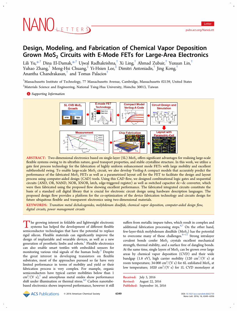
Design, Modeling, and Fabrication of Chemical Vapor DepositionGrown MoS2 Circuits with E‑Mode FETs for Large-Area ElectronicsLili Yu,*,† Dina El-Damak,*,† Ujwal Radhakrishna,† Xi Ling,† Ahmad Zubair,† Yuxuan Lin,†
Yuhao Zhang,† Meng-Hsi Chuang,‡ Yi-Hsien Lee,‡ Dimitri Antoniadis,† Jing Kong,†
Anantha Chandrakasan,† and Tomas Palacios†
†Massachusetts Institute of Technology, 77 Massachusetts Avenue, Cambridge, Massachusetts 02139, United States‡Materials Science and Engineering, National Tsing-Hua University, Hsinchu 30013, Taiwan
*S Supporting Information
ABSTRACT: Two-dimensional electronics based on single-layer (SL) MoS2 offers significant advantages for realizing large-scaleflexible systems owing to its ultrathin nature, good transport properties, and stable crystalline structure. In this work, we utilize agate first process technology for the fabrication of highly uniform enhancement mode FETs with large mobility and excellentsubthreshold swing. To enable large-scale MoS2 circuit, we also develop Verilog-A compact models that accurately predict theperformance of the fabricated MoS2 FETs as well as a parametrized layout cell for the FET to facilitate the design and layoutprocess using computer-aided design (CAD) tools. Using this CAD flow, we designed combinational logic gates and sequentialcircuits (AND, OR, NAND, NOR, XNOR, latch, edge-triggered register) as well as switched capacitor dc−dc converter, whichwere then fabricated using the proposed flow showing excellent performance. The fabricated integrated circuits constitute thebasis of a standard cell digital library that is crucial for electronic circuit design using hardware description languages. Theproposed design flow provides a platform for the co-optimization of the device fabrication technology and circuits design forfuture ubiquitous flexible and transparent electronics using two-dimensional materials.
KEYWORDS: Transition metal dichalcogenides, molybdenum disulfide, chemical vapor deposition, computer-aided design flow,digital circuits, power management circuits
The growing interest in foldable and lightweight electronicsystems has helped the development of different flexible
semiconductor technologies that have the potential to replacerigid silicon. Flexible materials can significantly improve thedesign of implantable and wearable devices, as well as a newgeneration of prosthetic limbs and robots.1 Flexible electronicscan also enable smart textiles with embedded sensors formonitoring various vital signals of the human body.2 Despitethe great interest in developing transistors on flexiblesubstrates, most of the approaches pursued so far have verylimited performance in terms of mobility and yield or theirfabrication process is very complex. For example, organicsemiconductors have typical carrier mobilities below than 1cm2/(V s),3 and amorphous metal oxides show performanceshift under illumination or thermal stress.4,5 Carbon nanotube-based electronics shows improved performance, however it still
suffers from metallic impure tubes, which result in complex andadditional fabrication processing steps.6,7 On the other hand,few-layer-thick molybdenum disulfide (MoS2) has the potentialto overcome many of these challenges.8−11 Strong intralayercovalent bonds confer MoS2 crystals excellent mechanicalstrength, thermal stability, and a surface free of dangling bonds.At the same time, single layers of MoS2 can be grown over largeareas by chemical vapor deposition (CVD) and their widebandgap (1.8 eV), high carrier mobility (120 cm2/(V s) atroom temperature; 34 000 cm2/(V s) for 6L exfoliated MoS2 atlow temperature; 1020 cm2/(V s) for 1L CVD monolayer at
Received: July 3, 2016Revised: August 22, 2016Published: September 16, 2016
Letter
pubs.acs.org/NanoLett
© 2016 American Chemical Society 6349 DOI: 10.1021/acs.nanolett.6b02739Nano Lett. 2016, 16, 6349−6356
low temperature),12 planar nature and mechanical flexibilitymake it an excellent candidate for the fabrication of transistorsfor both analog and digital circuits. Despite the promisingcharacteristics of MoS2, applications so far have been limited tosingle or few devices due to the many challenges associatedwith the uniformity and yield control in both material growthand device technology, as well as lack of an enhancement-mode(E-mode) transistor technology.10,13,14
In this work, we push the MoS2 technology forward bydemonstrating E-Mode transistors, compact modeling and acustom computer-aided design (CAD) flow to enable complexcircuits for the first time. First, we present a gate-first processwhere all the passive components are fabricated before theMoS2 transfer. This approach minimizes the fixed-charge in thegate dielectric of MoS2 transistors. This results in MoS2transistors with small subthreshold voltage swing and positivethreshold voltage and tight statistical distribution, which isessential for the successful design of multistage cascadedcircuits. Second, compact virtual source device models are usedto capture the different regions of device performance(subthreshold, linear, saturation) and to predict future FETperformance as the fabrication process evolves. Third, wedevelop a CAD flow for the design, simulation, and layout ofMoS2-based circuits, using an industry-standard IC designenvironment. A variety of combinational (inverter, NAND,NOR, AND, OR, XOR, XNOR) and sequential logic circuits(latch, edge-triggered register) as well as switched capacitorDC-DC converter have been designed and characterizedshowing correct functionality. With the demonstrated fabrica-tion technology, modeling, and computer-aided design flow, weprovide a platform for the co-optimization of circuits anddevices using MoS2 while the fabricated circuits shows the greatpromise of the technology for realizing complex systems.The design of electronic circuits using new materials like
MoS2 is often based on intuition, and the performanceevaluation is conducted only after fabrication. Thus, researchersin emerging fields are able to take only limited advantage ofstate-of-the-art CAD software. A CAD flow typically includesphysical or empirical models of the active and passivecomponents, a circuit simulator for performance evaluation,parametrized layout cells, as well as verification tools forchecking that the layout is compliant with design rules (such asmetal spacing) as well as for comparing the layout versus theschematic. Thus, the CAD flow leads to a significant reductionin the time and consequently the cost of fabrication ofadvanced chips.In order to enable the fabrication of large scale flexible
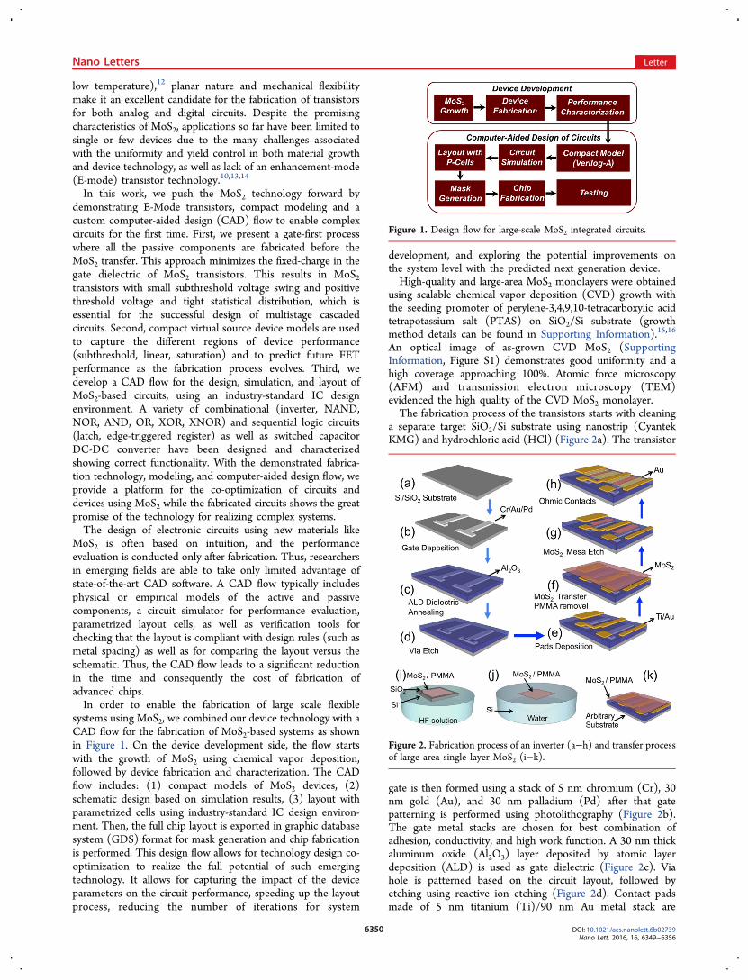
systems using MoS2, we combined our device technology with aCAD flow for the fabrication of MoS2-based systems as shownin Figure 1. On the device development side, the flow startswith the growth of MoS2 using chemical vapor deposition,followed by device fabrication and characterization. The CADflow includes: (1) compact models of MoS2 devices, (2)schematic design based on simulation results, (3) layout withparametrized cells using industry-standard IC design environ-ment. Then, the full chip layout is exported in graphic databasesystem (GDS) format for mask generation and chip fabricationis performed. This design flow allows for technology design co-optimization to realize the full potential of such emergingtechnology. It allows for capturing the impact of the deviceparameters on the circuit performance, speeding up the layoutprocess, reducing the number of iterations for system
development, and exploring the potential improvements onthe system level with the predicted next generation device.High-quality and large-area MoS2 monolayers were obtained
using scalable chemical vapor deposition (CVD) growth withthe seeding promoter of perylene-3,4,9,10-tetracarboxylic acidtetrapotassium salt (PTAS) on SiO2/Si substrate (growthmethod details can be found in Supporting Information).15,16
An optical image of as-grown CVD MoS2 (SupportingInformation, Figure S1) demonstrates good uniformity and ahigh coverage approaching 100%. Atomic force microscopy(AFM) and transmission electron microscopy (TEM)evidenced the high quality of the CVD MoS2 monolayer.The fabrication process of the transistors starts with cleaning
a separate target SiO2/Si substrate using nanostrip (CyantekKMG) and hydrochloric acid (HCl) (Figure 2a). The transistor
gate is then formed using a stack of 5 nm chromium (Cr), 30nm gold (Au), and 30 nm palladium (Pd) after that gatepatterning is performed using photolithography (Figure 2b).The gate metal stacks are chosen for best combination ofadhesion, conductivity, and high work function. A 30 nm thickaluminum oxide (Al2O3) layer deposited by atomic layerdeposition (ALD) is used as gate dielectric (Figure 2c). Viahole is patterned based on the circuit layout, followed byetching using reactive ion etching (Figure 2d). Contact padsmade of 5 nm titanium (Ti)/90 nm Au metal stack are
Figure 1. Design flow for large-scale MoS2 integrated circuits.
Figure 2. Fabrication process of an inverter (a−h) and transfer processof large area single layer MoS2 (i−k).
Nano Letters Letter
DOI: 10.1021/acs.nanolett.6b02739Nano Lett. 2016, 16, 6349−6356
6350
deposited before the MoS2 transfer (Figure 2e). As-grownMoS2 CVD sample is coated with poly(methyl methacrylate)(PMMA) as supporting layer and soaked in diluted HF solution(Figure 2i). The SiO2 layer underneath the MoS2 is etchedaway and the MoS2/PMMA stack is then released (Figure 2j)and transferred to the prefabricated target substrate (Figures2f,k). O2 plasma is then used to isolate the MoS2 transistorchannels (Figure 2g). Ohmic contacts are formed by depositinga 90 nm Au layer (Figure 2h).For MoS2 FETs fabricated with the conventional gate-last
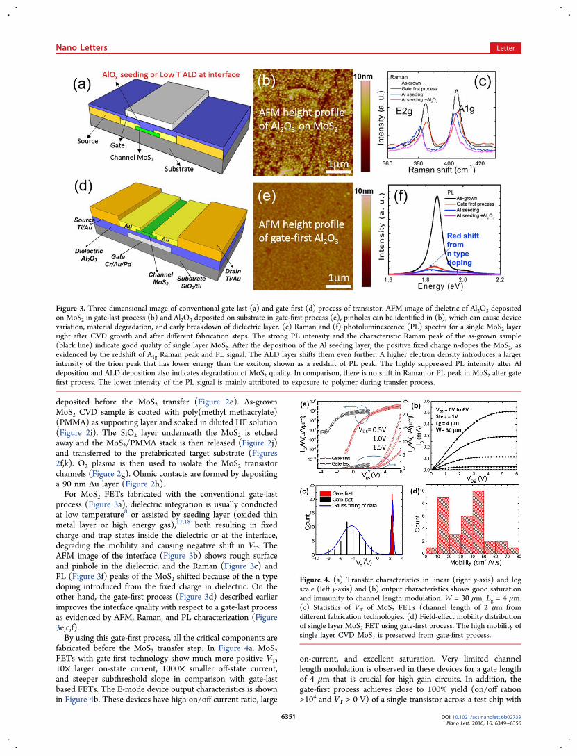
process (Figure 3a), dielectric integration is usually conductedat low temperature8 or assisted by seeding layer (oxided thinmetal layer or high energy gas),17,18 both resulting in fixedcharge and trap states inside the dielectric or at the interface,degrading the mobility and causing negative shift in VT. TheAFM image of the interface (Figure 3b) shows rough surfaceand pinhole in the dielectric, and the Raman (Figure 3c) andPL (Figure 3f) peaks of the MoS2 shifted because of the n-typedoping introduced from the fixed charge in dielectric. On theother hand, the gate-first process (Figure 3d) described earlierimproves the interface quality with respect to a gate-last processas evidenced by AFM, Raman, and PL characterization (Figure3e,c,f).By using this gate-first process, all the critical components are
fabricated before the MoS2 transfer step. In Figure 4a, MoS2FETs with gate-first technology show much more positive VT,10× larger on-state current, 1000× smaller off-state current,and steeper subthreshold slope in comparison with gate-lastbased FETs. The E-mode device output characteristics is shownin Figure 4b. These devices have high on/off current ratio, large
on-current, and excellent saturation. Very limited channellength modulation is observed in these devices for a gate lengthof 4 μm that is crucial for high gain circuits. In addition, thegate-first process achieves close to 100% yield (on/off ration>104 and VT > 0 V) of a single transistor across a test chip with
Figure 3. Three-dimensional image of conventional gate-last (a) and gate-first (d) process of transistor. AFM image of dieletric of Al2O3 depositedon MoS2 in gate-last process (b) and Al2O3 deposited on substrate in gate-first process (e), pinholes can be identified in (b), which can cause devicevariation, material degradation, and early breakdown of dielectric layer. (c) Raman and (f) photoluminescence (PL) spectra for a single MoS2 layerright after CVD growth and after different fabrication steps. The strong PL intensity and the characteristic Raman peak of the as-grown sample(black line) indicate good quality of single layer MoS2. After the deposition of the Al seeding layer, the positive fixed charge n-dopes the MoS2, asevidenced by the redshift of A1g Raman peak and PL signal. The ALD layer shifts them even further. A higher electron density introduces a largerintensity of the trion peak that has lower energy than the exciton, shown as a redshift of PL peak. The highly suppressed PL intensity after Aldeposition and ALD deposition also indicates degradation of MoS2 quality. In comparison, there is no shift in Raman or PL peak in MoS2 after gatefirst process. The lower intensity of the PL signal is mainly attributed to exposure to polymer during transfer process.
Figure 4. (a) Transfer characteristics in linear (right y-axis) and logscale (left y-axis) and (b) output characteristics shows good saturationand immunity to channel length modulation. W = 30 μm, Lg = 4 μm.(c) Statistics of VT of MoS2 FETs (channel length of 2 μm fromdifferent fabrication technologies. (d) Field-effect mobility distributionof single layer MoS2 FET using gate-first process. The high mobility ofsingle layer CVD MoS2 is preserved from gate-first process.
Nano Letters Letter
DOI: 10.1021/acs.nanolett.6b02739Nano Lett. 2016, 16, 6349−6356
6351
more than 200 FETs. Uniformity and repeatability of transistorperformance are very critical to multistage large area complexintegrated circuits. Thus, it is more challenging to realizecomplex integrated circuits based on CVD single layer MoS2.compared to using single crystal MoS2 flakes, because of thevariation introduced by the multicrystalline nature of CVDMoS2.
15 The gate first process substantially improves thetransistor uniformity. Statistical study of the transistor perform-ance shows that gate-first devices have an average VT of 2.41 Vwith standard deviation of 0.17 V while those from gate-lastprocess have average VT of −4.20 V and much larger standarddeviation of 1.75 V (Figure 4c). The positive and tightdistribution of VT is critical for designing cascaded circuit withlarge noise margin. The mobility of E-mode MoS2 FETs havebeen extracted from tens of FETs (Figures 4d). The high room-temperature mobility (as high as 80 cm2/V·s) shows the smallcharge impurity scattering from the interface of the dielectric.The statistic distribution of device subthreshold swings alsoconfirms the excellent quality and interface of the dielectric(Supporting Information, Figure S3).After the device characterization, we utilize the long channel
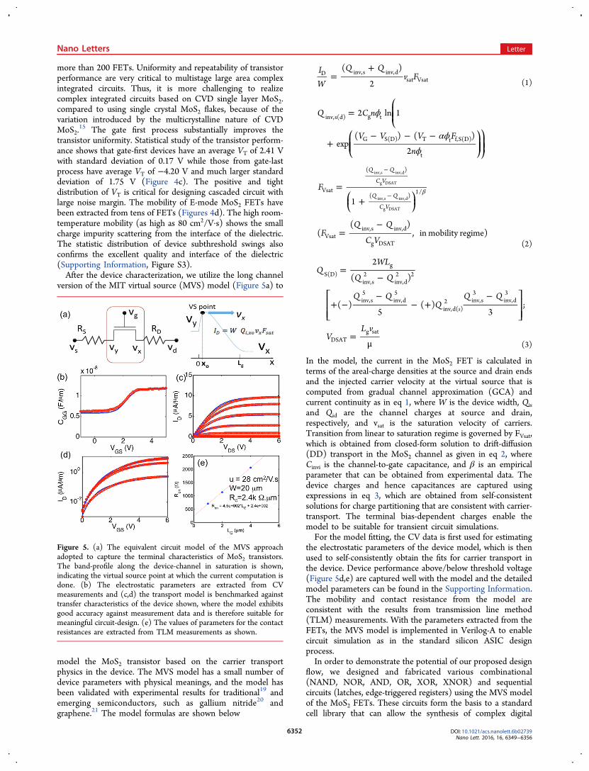
version of the MIT virtual source (MVS) model (Figure 5a) to
model the MoS2 transistor based on the carrier transportphysics in the device. The MVS model has a small number ofdevice parameters with physical meanings, and the model hasbeen validated with experimental results for traditional19 andemerging semiconductors, such as gallium nitride20 andgraphene.21 The model formulas are shown below
=+I
W
Q Qv F
( )
2D inv,s inv,d
sat Vsat (1)
ϕ
αϕϕ
=
+− − −
=+
=−
β
−
−⎜ ⎟
⎛⎝⎜⎜
⎛⎝⎜⎜
⎞⎠⎟⎟⎞⎠⎟⎟
⎛⎝
⎞⎠
Q C n
V V V F
n
F
FQ Q
C V
2 ln 1
exp( ) ( )
2
1
(( )
, in mobility regime)
Q Q
C V
Q Q
C V
inv,s(d) g t
G S(D) T t f,S(D)
t
Vsat
( )
( ) 1/
Vsatinv,s inv,d
g DSAT
inv,s inv,d
g DSAT
inv,s inv,d
g DSAT
(2)
=−
+ −−
− +−
=μ
⎡⎣⎢⎢
⎤⎦⎥⎥
QWL
Q Q
Q QQ
Q Q
VL v
2
( )
( )5
( )3
;s
S(D)g
inv,s2
inv,d2 2
inv,s5
inv,d5
inv,d( )2 inv,s
3inv,d3
DSATg sat
(3)
In the model, the current in the MoS2 FET is calculated interms of the areal-charge densities at the source and drain endsand the injected carrier velocity at the virtual source that iscomputed from gradual channel approximation (GCA) andcurrent continuity as in eq 1, where W is the device width, Qisand Qid are the channel charges at source and drain,respectively, and vsat is the saturation velocity of carriers.Transition from linear to saturation regime is governed by FVsat,which is obtained from closed-form solution to drift-diffusion(DD) transport in the MoS2 channel as given in eq 2, whereCinvi is the channel-to-gate capacitance, and β is an empiricalparameter that can be obtained from experimental data. Thedevice charges and hence capacitances are captured usingexpressions in eq 3, which are obtained from self-consistentsolutions for charge partitioning that are consistent with carrier-transport. The terminal bias-dependent charges enable themodel to be suitable for transient circuit simulations.For the model fitting, the CV data is first used for estimating
the electrostatic parameters of the device model, which is thenused to self-consistently obtain the fits for carrier transport inthe device. Device performance above/below threshold voltage(Figure 5d,e) are captured well with the model and the detailedmodel parameters can be found in the Supporting Information.The mobility and contact resistance from the model areconsistent with the results from transmission line method(TLM) measurements. With the parameters extracted from theFETs, the MVS model is implemented in Verilog-A to enablecircuit simulation as in the standard silicon ASIC designprocess.In order to demonstrate the potential of our proposed design
flow, we designed and fabricated various combinational(NAND, NOR, AND, OR, XOR, XNOR) and sequentialcircuits (latches, edge-triggered registers) using the MVS modelof the MoS2 FETs. These circuits form the basis to a standardcell library that can allow the synthesis of complex digital
Figure 5. (a) The equivalent circuit model of the MVS approachadopted to capture the terminal characteristics of MoS2 transistors.The band-profile along the device-channel in saturation is shown,indicating the virtual source point at which the current computation isdone. (b) The electrostatic parameters are extracted from CVmeasurements and (c,d) the transport model is benchmarked againsttransfer characteristics of the device shown, where the model exhibitsgood accuracy against measurement data and is therefore suitable formeaningful circuit-design. (e) The values of parameters for the contactresistances are extracted from TLM measurements as shown.
Nano Letters Letter
DOI: 10.1021/acs.nanolett.6b02739Nano Lett. 2016, 16, 6349−6356
6352
systems (such as a microprocessor) using hardware descriptionlanguages. Moreover, we designed and fabricated switchedcapacitor dc−dc converter for voltage scaling using theproposed flow.Logic gates are designed typically using pull-up and pull-
down networks; the former is connected between the supplyand the output node while the latter is connected between theoutput node and ground. In standard Si CMOS technology, thepull-up network is designed using pMOS transistors to allowrail-to-rail operation at a low power consumption.22 If theoutput is logic high in such case, the transistors in the pull-upnetwork will provide a low restive path to the supply, while thetransistors in the pull-down network will be operating in deepsubthreshold. Consequently, the logic level high in steady stateis equal to VDD less ILeakPDRPUH, where ILeakPD is the leakagecurrent of the gate set by the pull-down network and RPUH isthe equivalent resistance of pull-up network while the output ishigh. Similarly, the logic level low in steady state is equal toILeakPURPDL where ILeakPU is the leakage current set by the pull-up network and RPDL is the equivalent resistance of the pull-down network while the output is low. When the pull-up andthe pull-down networks are designed using pMOS and nMOSdevices, respectively, ILeakPDRPUH and ILeakPURPDL are smallenough such that the logic high and low levels are almost equalto VDD and GND, respectively, while being highly independentof the transistor sizing.22
The existing MoS2 technology lacks pMOS devices. MoS2 isnatively n-type as the material is subject to sulfur vacanciesduring the CVD growth process resulting in intrinsic electronconcentration.23 It is very challenging to fabricate pMOS fromMoS2 because of the trapping states, difficulty of doping MoS2,and the lack of good contact methods to p-type MoS2transistors. In particular, current technology of high energyion implantation for doping silicon is not applicable to MoS2because of its ultrathin structure. Consequently, the pull-upnetwork in any logic gate made of MoS2 has to be made of n-MOS.In order to realize rail-to-rail output swing, high noise
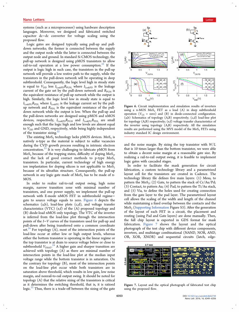
margin, narrow transition zone with minimal number oftransistors, and one power supply, we implement the pull-upnetwork with E-mode nMOS FET in subthreshold regime−gate to source voltage equals to zero. Figure 6 depicts theschematics (a,b), load-line plots (c,d), and voltage transfercharacteristics (VTC) (e,f) of the (A) proposed topology and(B) diode-load nMOS only topology. The VTC of the inverteris inferred from the load-line plot through the intersectionpoints of the I−V curves of the transistors used for pull-up andpull-down after being transferred onto a common coordinateset.24 For topology (A), most of the intersection points of theload-line occur at either low or high output levels, whereaseither the bottom transistor is operating in the linear regime orthe top transistor is at drain to source voltage below or close tosubthreshold VDSAT.
24 A higher gain and sharper transition areachieved with topology (A) as there are minimal number ofintersection points in the load-line plot at the median inputvoltage range while the bottom transistor is in saturation. Onthe contrary for topology (B), most of the intersection pointson the load-line plot occur while both transistors are insaturation above threshold, which results in low gain, low noisemargin, and nonrail-to-rail output swing. It should be noted fortopology (A) that the relative sizing of the transistors is criticalas it determines the switching threshold, that is, it is ratioedlogic.22 Thus, there is a trade-off between the sizing of the gate
and the noise margin. By sizing the top transistor with W/Lthat is 10 times larger than the bottom transistor, we were ableto obtain a decent noise margin at a reasonable gate size. Byrealizing a rail-to-rail output swing, it is feasible to implementlogic gates with cascaded stages.In order to facilitate the mask generation for circuit
fabrication, a custom technology library and a parametrizedlayout cell for the transistors are created in Cadence. Thetechnology library file defines five main layers: (1) Mesa, topattern the MoS2; (2) Gate, to pattern the stack of Cr/Au/Pd;(3) Contact, to pattern Au; (4) Pad, to pattern the Ti/Au stack,and (5) Via, to define the holes used for creating connectionfrom the gate layer to the pad layer. The parametrized layoutcell allows the scaling of the width and length of the channelwhile maintaining a fixed overlap between the contacts and theMoS2 (Supporting Information Figure S3). After the generationof the layout of each FET in a circuit, the placement androuting (using Pad and Gate layers) are done manually. Then,the full chip layout is exported in GDS format for maskfabrication. Figure 7 shows the layout and the opticalphotograph of the test chip with different device components,inverters, and multistage combinational (NAND, NOR, AND,OR, XOR, XNOR) and sequential circuits (latch, edge-
Figure 6. Circuit implementation and simulation results of invertersusing a n-MOS MoS2 FET as a load (A) in deep subthresholdoperation (VGS = zero) and (B) in diode-connected configuration.(a,b) Schematics of topology (A,B) respectively; (c,d) load-line plotfor topology (A,B) respectively; (e,f) voltage transfer characteristics ofthe inverter using topology (A,B) respectively. All the simulationresults are performed using the MVS model of the MoS2 FETs usingindustry standard IC design environment.
Figure 7. Layout and the optical photograph of fabricated test chipusing the proposed flow.
Nano Letters Letter
DOI: 10.1021/acs.nanolett.6b02739Nano Lett. 2016, 16, 6349−6356
6353
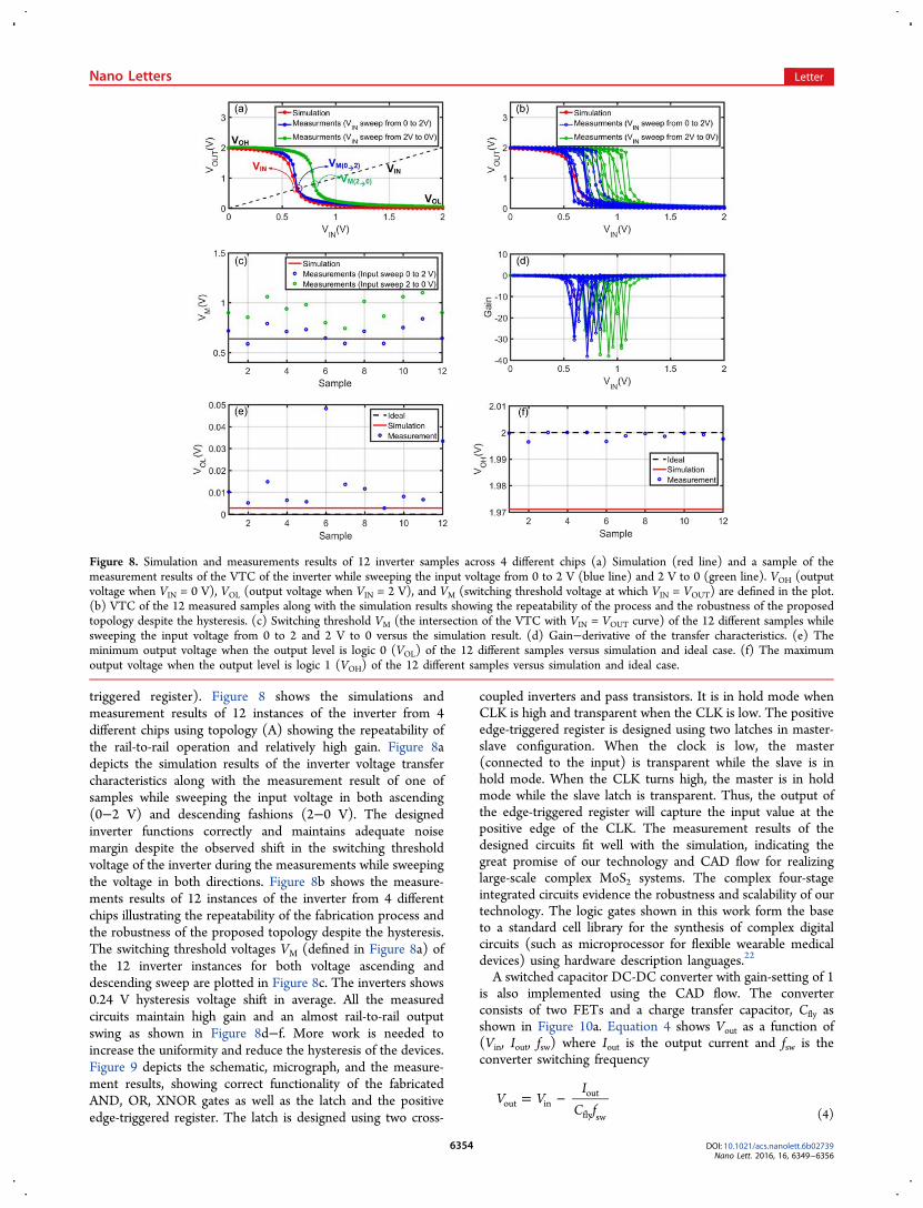
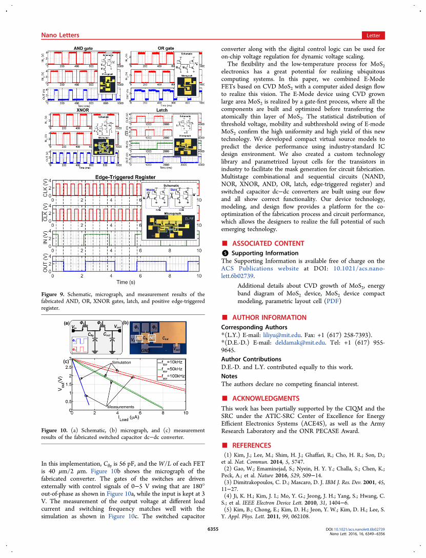
triggered register). Figure 8 shows the simulations andmeasurement results of 12 instances of the inverter from 4different chips using topology (A) showing the repeatability ofthe rail-to-rail operation and relatively high gain. Figure 8adepicts the simulation results of the inverter voltage transfercharacteristics along with the measurement result of one ofsamples while sweeping the input voltage in both ascending(0−2 V) and descending fashions (2−0 V). The designedinverter functions correctly and maintains adequate noisemargin despite the observed shift in the switching thresholdvoltage of the inverter during the measurements while sweepingthe voltage in both directions. Figure 8b shows the measure-ments results of 12 instances of the inverter from 4 differentchips illustrating the repeatability of the fabrication process andthe robustness of the proposed topology despite the hysteresis.The switching threshold voltages VM (defined in Figure 8a) ofthe 12 inverter instances for both voltage ascending anddescending sweep are plotted in Figure 8c. The inverters shows0.24 V hysteresis voltage shift in average. All the measuredcircuits maintain high gain and an almost rail-to-rail outputswing as shown in Figure 8d−f. More work is needed toincrease the uniformity and reduce the hysteresis of the devices.Figure 9 depicts the schematic, micrograph, and the measure-ment results, showing correct functionality of the fabricatedAND, OR, XNOR gates as well as the latch and the positiveedge-triggered register. The latch is designed using two cross-
coupled inverters and pass transistors. It is in hold mode whenCLK is high and transparent when the CLK is low. The positiveedge-triggered register is designed using two latches in master-slave configuration. When the clock is low, the master(connected to the input) is transparent while the slave is inhold mode. When the CLK turns high, the master is in holdmode while the slave latch is transparent. Thus, the output ofthe edge-triggered register will capture the input value at thepositive edge of the CLK. The measurement results of thedesigned circuits fit well with the simulation, indicating thegreat promise of our technology and CAD flow for realizinglarge-scale complex MoS2 systems. The complex four-stageintegrated circuits evidence the robustness and scalability of ourtechnology. The logic gates shown in this work form the baseto a standard cell library for the synthesis of complex digitalcircuits (such as microprocessor for flexible wearable medicaldevices) using hardware description languages.22
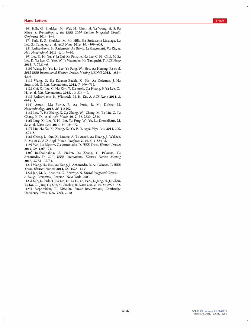
A switched capacitor DC-DC converter with gain-setting of 1is also implemented using the CAD flow. The converterconsists of two FETs and a charge transfer capacitor, Cfly asshown in Figure 10a. Equation 4 shows Vout as a function of(Vin, Iout, fsw) where Iout is the output current and fsw is theconverter switching frequency
−=V VI
C fout inout
fly sw (4)
Figure 8. Simulation and measurements results of 12 inverter samples across 4 different chips (a) Simulation (red line) and a sample of themeasurement results of the VTC of the inverter while sweeping the input voltage from 0 to 2 V (blue line) and 2 V to 0 (green line). VOH (outputvoltage when VIN = 0 V), VOL (output voltage when VIN = 2 V), and VM (switching threshold voltage at which VIN = VOUT) are defined in the plot.(b) VTC of the 12 measured samples along with the simulation results showing the repeatability of the process and the robustness of the proposedtopology despite the hysteresis. (c) Switching threshold VM (the intersection of the VTC with VIN = VOUT curve) of the 12 different samples whilesweeping the input voltage from 0 to 2 and 2 V to 0 versus the simulation result. (d) Gain−derivative of the transfer characteristics. (e) Theminimum output voltage when the output level is logic 0 (VOL) of the 12 different samples versus simulation and ideal case. (f) The maximumoutput voltage when the output level is logic 1 (VOH) of the 12 different samples versus simulation and ideal case.
Nano Letters Letter
DOI: 10.1021/acs.nanolett.6b02739Nano Lett. 2016, 16, 6349−6356
6354
In this implementation, Cfly is 56 pF, and the W/L of each FETis 40 μm/2 μm. Figure 10b shows the micrograph of thefabricated converter. The gates of the switches are drivenexternally with control signals of 0−5 V swing that are 180°out-of-phase as shown in Figure 10a, while the input is kept at 3V. The measurement of the output voltage at different loadcurrent and switching frequency matches well with thesimulation as shown in Figure 10c. The switched capacitor
converter along with the digital control logic can be used foron-chip voltage regulation for dynamic voltage scaling.The flexibility and the low-temperature process for MoS2
electronics has a great potential for realizing ubiquitouscomputing systems. In this paper, we combined E-ModeFETs based on CVD MoS2 with a computer aided design flowto realize this vision. The E-Mode device using CVD grownlarge area MoS2 is realized by a gate-first process, where all thecomponents are built and optimized before transferring theatomically thin layer of MoS2. The statistical distribution ofthreshold voltage, mobility and subthreshold swing of E-modeMoS2 confirm the high uniformity and high yield of this newtechnology. We developed compact virtual source models topredict the device performance using industry-standard ICdesign environment. We also created a custom technologylibrary and parametrized layout cells for the transistors inindustry to facilitate the mask generation for circuit fabrication.Multistage combinational and sequential circuits (NAND,NOR, XNOR, AND, OR, latch, edge-triggered register) andswitched capacitor dc−dc converters are built using our flowand all show correct functionality. Our device technology,modeling, and design flow provides a platform for the co-optimization of the fabrication process and circuit performance,which allows the designers to realize the full potential of suchemerging technology.
■ ASSOCIATED CONTENT*S Supporting InformationThe Supporting Information is available free of charge on theACS Publications website at DOI: 10.1021/acs.nano-lett.6b02739.
Additional details about CVD growth of MoS2, energyband diagram of MoS2 device, MoS2 device compactmodeling, parametric layout cell (PDF)
■ AUTHOR INFORMATIONCorresponding Authors*(L.Y.) E-mail: [email protected]. Fax: +1 (617) 258-7393).*(D.E.-D.) E-mail: [email protected]. Tel: +1 (617) 955-9645.Author ContributionsD.E.-D. and L.Y. contributed equally to this work.NotesThe authors declare no competing financial interest.
■ ACKNOWLEDGMENTSThis work has been partially supported by the CIQM and theSRC under the ATIC-SRC Center of Excellence for EnergyEfficient Electronics Systems (ACE4S), as well as the ArmyResearch Laboratory and the ONR PECASE Award.
■ REFERENCES(1) Kim, J.; Lee, M.; Shim, H. J.; Ghaffari, R.; Cho, H. R.; Son, D.;et al. Nat. Commun. 2014, 5, 5747.(2) Gao, W.; Emaminejad, S.; Nyein, H. Y. Y.; Challa, S.; Chen, K.;Peck, A.; et al. Nature 2016, 529, 509−14.(3) Dimitrakopoulos, C. D.; Mascaro, D. J. IBM J. Res. Dev. 2001, 45,11−27.(4) Ji, K. H.; Kim, J. I.; Mo, Y. G.; Jeong, J. H.; Yang, S.; Hwang, C.S.; et al. IEEE Electron Device Lett. 2010, 31, 1404−6.(5) Kim, B.; Chong, E.; Kim, D. H.; Jeon, Y. W.; Kim, D. H.; Lee, S.Y. Appl. Phys. Lett. 2011, 99, 062108.
Figure 9. Schematic, micrograph, and measurement results of thefabricated AND, OR, XNOR gates, latch, and positive edge-triggeredregister.
Figure 10. (a) Schematic, (b) micrograph, and (c) measurementresults of the fabricated switched capacitor dc−dc converter.
Nano Letters Letter
DOI: 10.1021/acs.nanolett.6b02739Nano Lett. 2016, 16, 6349−6356
6355
(6) Hills, G.; Shulaker, M.; Wei, H.; Chen, H. Y.; Wong, H. S. P.;Mitra, S. Proceedings of the IEEE 2014 Custom Integrated CircuitsConference 2014, 1−4.(7) Park, R. S.; Shulaker, M. M.; Hills, G.; Suriyasena Liyanage, L.;Lee, S.; Tang, A.; et al. ACS Nano 2016, 10, 4599−608.(8) Radisavljevic, B.; Radenovic, A.; Brivio, J.; Giacometti, V.; Kis, A.Nat. Nanotechnol. 2011, 6, 147−50.(9) Lee, G. H.; Yu, Y. J.; Cui, X.; Petrone, N.; Lee, C. H.; Choi, M. S.;Lee, D. Y.; Lee, C.; Yoo, W. J.; Watanabe, K.; Taniguchi, T. ACS Nano2013, 7, 7931−6.(10) Wang, H.; Yu, L.; Lee, Y.; Fang, W.; Hsu, A.; Herring, P.; et al.2012 IEEE International Electron Devices Meeting (IEDM) 2012, 4.6.1−4.6.4.(11) Wang, Q. H.; Kalantar-Zadeh, K.; Kis, A.; Coleman, J. N.;Strano, M. S. Nat. Nanotechnol. 2012, 7, 699−712.(12) Cui, X.; Lee, G.-H.; Kim, Y. D.; Arefe, G.; Huang, P. Y.; Lee, C.-H.; et al. Nat. Nanotechnol. 2015, 10, 534−40.(13) Radisavljevic, B.; Whitwick, M. B.; Kis, A. ACS Nano 2011, 5,9934−8.(14) Amani, M.; Burke, R. A.; Proie, R. M.; Dubey, M.Nanotechnology 2015, 26, 115202.(15) Lee, Y.-H.; Zhang, X.-Q.; Zhang, W.; Chang, M.-T.; Lin, C.-T.;Chang, K.-D.; et al. Adv. Mater. 2012, 24, 2320−2325.(16) Ling, X.; Lee, Y.-H.; Lin, Y.; Fang, W.; Yu, L.; Dresselhaus, M.S.; et al. Nano Lett. 2014, 14, 464−72.(17) Liu, H.; Xu, K.; Zhang, X.; Ye, P. D. Appl. Phys. Lett. 2012, 100,152115.(18) Cheng, L.; Qin, X.; Lucero, A. T.; Azcatl, A.; Huang, J.; Wallace,R. M.; et al. ACS Appl. Mater. Interfaces 2014, 6, 11834−8.(19) Wei, L.; Mysore, O.; Antoniadis, D. IEEE Trans. Electron Devices2012, 59, 1263−71.(20) Radhakrishna, U.; Piedra, D.; Zhang, Y.; Palacios, T.;Antoniadis, D. 2013 IEEE International Electron Devices Meeting2013, 32.7.1−32.7.4.(21) Wang, H.; Hsu, A.; Kong, J.; Antoniadis, D. A.; Palacios, T. IEEETrans. Electron Devices 2011, 58, 1523−1533.(22) Jan, M. R.; Anantha, C.; Borivoje, N. Digital Integrated Circuits −A Design Perspective; Pearson: New York, 2003(23) Suh, J.; Park, T. E.; Lin, D. Y.; Fu, D.; Park, J.; Jung, H. J.; Chen,Y.; Ko, C.; Jang, C.; Sun, Y.; Sinclair, R. Nano Lett. 2014, 14, 6976−82.(24) Sarpheshkar, R. Ultra-low Power Bioelectronics; CambridgeUniversity Press: New York, 2010.
Nano Letters Letter
DOI: 10.1021/acs.nanolett.6b02739Nano Lett. 2016, 16, 6349−6356
6356