Embed Size (px)
Citation preview
Université du Québec
Institut National de la Recherche Scientifique
Centre Énergie, Matériaux et Télécommunications
Génération et traitement du signal optique basés sur le
filtrage linéaire de phase-seule dans les domaines temporel et
spectral
Par
Reza Maram Qartavol
Thèse présentée pour l’obtention du grade de
Doctorat en Télécommunication, Ph.D.
Jury d’évaluation
Examinateur externe Carlos R. Fernandez-Pousa
Universidad Miguel Hernández de Elche,
Spain
Examinateur externe Shulabh Gupta
Carleton University, Canada
Examinateur interne Luca Razzari
INRS-EMT, Canada
Directeur de recherche José Azaña
INRS-EMT, Canada

ii

iii
Pour mes parents et Samané
To my parents and Samane

iv

v
Acknowledgements
“If I have seen further it is only by standing on the shoulders of giants.”
Isaac Newton
To begin, I would like to acknowledge the whole Canadian continent and, in particular,
Montréal for being such an amazing place. A combination of a tech-savvy society, world-class
scientific community, down-to-earth people and a vibrant ecosystem make it doubtlessly the best
location on the globe for accomplishing a PhD in optical telecom.
As part of this scientific community, José Azaña is the person who gave me the opportunity to
join the UOP family. Living 30 milliseconds of fiber optic latency away from home — or around
18 hours by plane — is an everyday challenge that can only be taken up with the support of an
adoptive family which I partly found in the friendly UOP team at INRS-EMT. Among them, José
Azaña, my supervisor, is the one who guided me at light speed through this scientific journey. His
guidance, counsel and attitude pushed me to do my best on my current projects while keeping a
place for imagination and new ideas. He taught me valuable lessons not only to become a better
researcher and scientific professional, but also a better person in life. It has been an honor to work
with him and learn so much from him. José, thanks so much for everything you have done for me.
I would like to deeply thank my lovely wife Samaneh for her constant support, help, care,
encouragement, laughter and her mere company. She is my best friend and my companion in life.
I thank her for her sacrifice as I pursued my goals and dreams in graduation levels. No amount of
words is enough to express my true gratitude for her patience and for always being there. Samaneh,
I cannot imagine what my life would look like without you. I love you very much and I thank you
with all my heart for being such a great part of my life.
I also thank my parents, Ali and Fatemeh, for their unconditional love, support throughout my
life and your encouragement for pursuing my education. They have walked with me along good
and difficult times, and during this path, they have taught me to always think big and work hard to
achieve my goals. Their precious advice for life will always accompany me. They continue to
inspire me in every way of life and with all their love they have shown me how to succeed in all
vi
of life’s challenges. My deep thanks and lots of appreciation must go to my brothers, Hamed,
Mohammad, and Amir and my little sister, Zeinab, whose love and support from thousands of
kilometers away have always given me the energy to work and follow my dreams. Special gratitude
must also go to the members of my family-in-law, Hassan, Roghayeh, Hamid, Elahe, Saeede,
Alireza for their love and support. Thank you all.
I would like to give my special and sincere thanks to Prof. James Van Howe, from Augustana
College, IL, US, for being an excellent mentor entire my PhD studies and for the fruitful
discussions and collaborations on several of my projects. At the beginning of my PhD, Prof. Van
Howe joined our group for two months as a visiting professor. During this period, he taught me
valuable experimental techniques and theoretical analyses that will always be with me in my
professional career and I greatly appreciate his time and effort. He has a wonderful grasp on math
and physics, matched by an ability to explain them. Since then, we have been working together in
many common projects. It is always a pleasure to work, and share time and ideas with such
excellent and reputable professionals.
Prof. Leif Katsuo Oxenløwe and his group members, Deming Kong, Michael Galili, Francesco
Da Ros, Pengyu Guan, and Kasper Meldgaard Røge, from the Technical University of Denmark
(DTU), deserves special thanks for hosting me and the great collaboration during my two visits, in
total of 40days, to DTU. Their priceless assistance and suggestions and supplying state-of-the-art
lab equipment have helped me to successfully carry out several of my projects presented in this
Thesis.
I am indebted to all past, present and honouree members of the UOP Lab: Dr. Reza Ashrafi,
Dr. Maurizio Burla, Dr. Hossein Asghari, Dr. Hugues Guillet de Chatellus, Dr. Ming Li, Dr.
Mohamed Seghilani, Dr. Bo Li, Dr. Lei Lei, Dr. Alejandro Carballar, Dr. Antonio Malacarne, Dr.
María del Rosario Fernández Ruiz, Dr. Hamed Pishvai Bazargani, Luis Romero Cortés, Jeonh
Hyun Huh, Jinwoo Jeon, and Sai krishna reddy. Thank you so much for your help but most
importantly for your friendship. In particular, I would like to thank Luis Romero Cortés who
helped a great deal in several of project conducted in this Thesis. Also, special thanks to Dr. Reza
Ashrafi, for great times and discussions we had at Park-Milton Presse Café for learning new things
on weekends. Additionally, I would like to thank the staff from the INRS-EMT.
vii
My sincere gratitude goes to the core committee for my Ph.D Thesis: Prof. Luca Razzari, Prof.
Carlos R. Fernandez-Pousa and Prof. Shulabh Gupta. Thank you for your time and efforts in
reviewing my Thesis.
Finally, I thank le Fonds Québécois de la Recherche sur la Nature et les Technologies
(FQRNT), and Institut National de la Recherche Scientifique – Énergie, Matériaux et
Télécommunications (INRS-EMT), for providing the funding which allowed me to undertake this
PhD research.
Reza Maram

viii
ix
Résumé
Les exigences sans cesse croissantes du trafic de données dans les services de
télécommunication conduisent à un besoin continu de capacités de réseau plus élevés. Dans ce
scénario, le débit binaire dans un canal de longueur d’onde ainsi que le nombre de canaux ne
cessent d’augmenter dans les réseaux de télécommunication grâce aux progrès des technologies
de transmission optiques. Aujourd’hui, les systèmes de multiplexage en longueur d’onde (WDM
pour wavelength division multiplexing en anglais) supportent des capacités de transmission
d’environ 14 Tbit/s, des milliers de fois plus élevé que la capacité de toute autre liaison de
transmission (par exemple ondes radio et téléphonie), ce débit est réalisé par le multiplexage de
plusieurs centaines de longueurs d’onde avec un débit binaire de ~ 40 Gbit /s par canal. Cependant,
le signal lumineux porteur d’information doit être converti à un signal électronique compatible
avec les routeurs/commutateurs dans les réseaux de télécommunication. Dans cette conversion, le
débit d’information est considérablement ralenti en raison du déséquilibre de bande passante entre
la transmission optique et les routeurs électroniques. Le traitement du signal optique est une
solution alternative potentielle très prometteuse aux problèmes liés à l’électronique. Récemment,
un effort considérable a été investi dans le développement des méthodes optiques ultrarapides de
traitement du signal pour les applications dans les réseaux de fibre optique, les plateformes de
traitement de l’information et d’informatique optique à haute vitesse. Cependant, en pratique, la
vitesse de traitement est seulement une des plusieurs questions importantes à prendre en
considération lors du déploiement de nouvelles technologies de traitement. L’une des principales
raisons pour lesquelles le traitement électronique du signal est préféré actuellement sur d’autres
alternatives, en particulier sur le traitement du signal optique, est que les appareils électroniques
consomment relativement moins d’énergie. Contrairement à l’électronique, la plupart des
processeurs optiques proposés à ce jour, typiquement basés sur des effets "non linéaires",
nécessiteraient une consommation d’énergie peu pratique, plus élevée de plusieurs ordres de
grandeur que celle des processeurs électroniques lorsqu’ils sont utilisés dans des situations réelles
et à pleine échelle. En effet, la performance énergétique médiocre des méthodes de traitement du
signal optique entrave considérablement leur capacité à offrir une solution pratique et compétitive
pour le traitement du signal.
x
Afin de maintenir une pénétration accrue de l’optique dans les futurs systèmes de traitement
et aider à réaliser la transition de technologie de l’électronique à l’optique dans les plateformes de
traitement de l’information et de calcul, des processeurs optiques écoénergétiques innovants
doivent être conçus et développés pour effectuer les tâches nécessaires, idéalement avec une perte
minimale de l’énergie du signal d’entrée et une utilisation réduite de l’alimentation externe
supplémentaire. Dans cet objectif, il faut étudier la possibilité d’utiliser des techniques linéaires
purement passives pour le traitement du signal optique, en évitant l’utilisation de mécanismes
actifs et /ou non linéaires conventionnels dans les dispositifs de traitement du signal. Ces
mécanismes nécessitent une alimentation externe suffisamment élevée et/ou
consomment/dissipent une partie importante de l’énergie du signal entrant. En revanche, le
traitement du signal basé uniquement sur des composants optiques linéaires passifs, offre la
possibilité de mettre en œuvre des circuits de traitement qui permettent fondamentalement une
consommation nulle de l’énergie du signal tout en évitant l’utilisation d’une source supplémentaire
de lumière.
Dans cette thèse, je considère l’utilisation des procédés purement linéaires pour manipuler les
profils temporel et spectrale du signal sous test, à savoir la modulation temporelle linéaire et le
filtrage spectral linéaire, respectivement. La manipulation désirée peut être produite sur le profil
amplitude du signal sous test par modulation temporelle d’intensité ou filtrage spectral
d’amplitude. Si aucun gain supplémentaire n’est utilisé dans le système ciblé (régime passive), la
modulation d’intensité ou le filtrage d’amplitude produit nécessairement une perte d’une partie de
l’énergie du signal d’entrée. En fonction de la fonctionnalité ciblée, les pertes de
modulation/filtrage peuvent être considérables. En revanche, l’énergie du signal peut être
entièrement préservée si seule la phase du signal est manipulée dans le domaine temporel, c.-à-d.
par filtrage spectrale de phase.
Dans l’ensemble, les nouveaux systèmes de traitement optique des signaux proposés dans ma
thèse sont basés sur une combinaison appropriée de la modulation temporelle linéaire de phase-
seule et les processus de filtrage spectral, conduisant à la mise en œuvre de la fonctionnalité
souhaitée avec un rendement énergétique optimisé. Ce résultat est obtenu sans compromis sur les
avantages de traitement du signal intrinsèque à l’optique. Dans les processeurs proposés dans cette
thèse, l’énergie du signal entrant est efficacement redistribuée pour construire le signal de sortie
xi
ciblé sans l’utilisation d’aucune puissance optique externe supplémentaire. J’utilise cette approche
pour la mise en œuvre d’une série d’importantes fonctionnalités de traitement du signal. En
particulier, dans le chapitre 2, nous utilisons la combinaison des effets Talbot temporel et spectral,
impliquant la modulation de phase temporelle et le filtrage de phase spectrale, pour contrôler et
programmer le taux de répétition et l’énergie par impulsion associée d’une source laser
impulsionnelle à faible taux de répétition d’impulsions. Dans le chapitre 3, nous démontrons une
nouvelle approche tout-optique efficace énergétiquement pour la conversion de format de données
de télécommunication optique: retour-à-zéro (RZ) au non-retour-à-zéro (NRZ). Cette approche a
été mise en œuvre expérimentalement avec un débit binaire de 640 Gbit/s. Nous démontrons
également d’autres nouvelles approches de récupération des signaux d’horloge de base et sous-
harmonique à partir de signaux de données de type tout-ou-rien (OOK pour on-off-keying en
anglais). Ce travail de recherche peut ouvrir de nouvelles perspectives importantes pour la mise en
œuvre d’autres processeurs optiques critiques avec une efficacité énergétique sans précédent,
dépassant les limites de consommation d’énergie des technologies optiques actuelles sans perdre
leur avantage en matière de vitesse de traitement.

xii
xiii
Abstract
The ever-increasing data traffic requirements in telecommunication services lead to a
continuous need for higher network capabilities. In this scenario, the bit rate of one wavelength
channel and the number of channels keep increasing in telecommunication networks thanks to the
advancement of optical transmission technologies. Nowadays, wavelength division multiplexing
(WDM) systems support transmission capabilities of about 14 Tbit/s, through multiplexing of
several hundred wavelengths with a single channel bit rate of ∼ 40 Gbit/s, thousands of times
higher than any other transmission link (e.g. direct radio and telephone links) capacity. However,
light information has to be converted to electrons when accessed by electronic routers/switches in
the telecommunication networks. In that conversion, information is significantly slowed down due
to the bandwidth imbalance between the optical transmissions and electronic routers. Optical
signal processing is a very promising potential alternative solution to the problems associated with
electronics. Recently, there has been a significant effort toward the realization of ultrafast optical
signal processing methods for applications in next-generation fiber-optic networks and high-speed
information processing and optical computing platforms. However, in practice, processing speed
is only one of the several important issues to be considered when deploying new processing
technology. One of the main reasons why electronic signal processing is preferred presently over
other alternatives, particularly over optical signal processing, is that electronic devices consume a
relatively smaller amount of energy. Unlike electronics, most optical processors proposed to date,
typically realized using “nonlinear” effects, would require unpractical power consumption, orders-
of-magnitude higher than that of their electronic counterparts, when used at a real-world scale.
Indeed, the poor energy performance of optical signal processing methods greatly hinders their
capability to offer a practical, competitive solution for signal processing.
In order to keep optics penetration deeper into future processing systems and help to realize
the technology shift from electronics to optics in information processing and computing platforms,
innovative energy-efficient optical signal processors should be designed and developed to perform
the needed tasks ideally with minimal loss of the input signal’s energy and reducing the use of
supplementary external power. To this end, one needs to explore the possibility of using purely
passive and linear techniques for optical signal processing, avoiding the use of conventional active
xiv
and/or nonlinear mechanisms in the signal-processing engines. These mechanisms require a
sufficiently high external power and/or consume/dissipate significant energy from the incoming
signal. In sharp contrast, signal processing based on only linear, passive optical components offers
the possibility of implementing processing circuits that fundamentally enable no signal power
consumption while avoiding the use of any additional optical light source.
In this Thesis, I consider the use of purely linear processes to manipulate the temporal and
spectral profiles of a signal under test, namely linear temporal modulation and linear spectral
filtering, respectively. The desired manipulation can be produced on the amplitude profile of the
signal under test through temporal intensity modulation or amplitude spectral filtering. If no
additional active gain is employed in the target system (passive scheme), intensity modulation or
amplitude filtering necessarily wastes some of the input signal’s energy. Depending on the target
functionality, modulation/filtering losses can be considerable. In sharp contrast, the signal energy
can be fully preserved if only the signal phase is manipulated in the time domain, i.e., by temporal
phase modulation, and/or in the frequency domain, i.e., by spectral phase filtering.
Generally, the novel optical signal-processing schemes proposed in my Thesis are based on a
suitable combination of phase-only linear temporal modulation and spectral filtering processes,
leading to the implementation of the desired functionality with an optimized energy performance.
This is achieved without trading the signal processing advantage intrinsic to optics. In my newly
proposed processors, the incoming signal’s energy is effectively redistributed to build up the target
output signal without using any additional external optical power. I am using this approach for
implementation of a range of important signal processing functionalities. In particular, in Chapter
2, we use the combination of the temporal and spectral Talbot effect, involving temporal phase
modulation and spectral phase filtering, to control and program the repetition-rate and associated
energy per pulse of a low-rate laser source. In Chapter 3, we demonstrate a novel energy-efficient
approach for all optical return-to-zero (RZ)-to-non-RZ (NRZ) telecommunication data format
conversion, experimentally implemented at a bit rate of 640 Gbit/s, and novel approaches for base-
rate and sub-harmonic clock recovery of on-off-keying (OOK) data signals. This research may
open new, important perspectives for implementing other critical optical signal processors with
unprecedented energy efficiency, overcoming the energy-consumption limitations of present
optical technologies without trading their processing speed advantage.

xv
xvi
Table des matières
Acknowledgements ................................................................................................................. v
Résumé .................................................................................................................................... ix
Abstract ................................................................................................................................ xiii
Table des matières ............................................................................................................... xvi
Liste des figures .................................................................................................................... xix
Publications associées ....................................................................................................... xxvii
Chapitre 1 ................................................................................................................................ 1
1 Introduction (en français) ................................................................................................ 1
1.1 Traitement du signal Transition de l’électronique à l’optique? ................................ 1
1.2 Traitement du signal optique et consommation d’énergie ...................................... 10 1.2.1 Traitement non-linéaire du signal optique ....................................................... 12
1.2.2 Traitement linéaire du signal optique .............................................................. 16 1.3 Revu des processeurs de signaux optiques pertinents étudiés dans cette thèse ...... 24
1.3.1 Récupération de l’horloge optique .................................................................. 24
1.3.2 Conversion de formats RZ à NRZ optiques .................................................... 29 1.3.3 Méthodes de génération des impulsions optiques picoseconde pour les systèmes
optiques à haute vitesse ......................................................................................................... 32
1.4 Objectif et Organisation de la Thèse ....................................................................... 38
Chapter 1 ............................................................................................................................... 43
1 Introduction ..................................................................................................................... 43
1.1 Signal processing: Transition from electronics to optics? ...................................... 43
1.2 Optical signal processing and energy consumption ................................................ 51 1.2.1 Nonlinear optical signal processing ................................................................. 52
1.2.2 Linear optical signal processing ...................................................................... 56 1.3 Review of relevant optical signal processors studied in this dissertation ............... 63
1.3.1 Optical Clock Recovery ................................................................................... 63
1.3.2 Optical RZ to NRZ format conversion ............................................................ 67 1.3.3 Optical picosecond pulse generation methods for high-speed optical systems 70
1.4 Objective and Organization of the Thesis ............................................................... 75
Chapter 2 ............................................................................................................................... 79
2 Energy-preserving pulse repetition-rate control for high-speed optical systems ..... 79
2.1 Introduction ............................................................................................................. 79 2.2 The Talbot effect ..................................................................................................... 80
2.2.1 Temporal Talbot effect .................................................................................... 85 2.2.2 The spectral Talbot effect ................................................................................ 95 2.2.3 Applications of temporal Talbot effect ............................................................ 97
xvii
2.2.4 Influence on random amplitude noise and timing jitter ................................. 102
2.2.5 Temporal phase variations in the temporal Talbot effect .............................. 105 2.3 Programmable Fiber-Optics Pulse Repetition-Rate Multiplier............................. 107
2.3.1 Abstract .......................................................................................................... 107
2.3.2 Introduction ................................................................................................... 107 2.3.3 Basic Operation Principle .............................................................................. 109 2.3.4 Design Equations ........................................................................................... 114 2.3.5 Time-Frequency Analysis.............................................................................. 115 2.3.6 Experimental demonstration of the programmable rate multiplier ............... 117
2.3.7 Conclusion ..................................................................................................... 121 2.4 Lossless fractional repetition-rate multiplication of optical pulse trains .............. 122
2.4.1 Abstract .......................................................................................................... 122 2.4.2 Introduction ................................................................................................... 122
2.4.3 The operation principle .................................................................................. 123 2.4.4 System design ................................................................................................ 125
2.4.5 Experimental demonstration .......................................................................... 126 2.4.6 Conclusion ..................................................................................................... 131
2.5 Noiseless Intensity Amplification of Repetitive Signals by Coherent Addition using
the Temporal Talbot Effect ..................................................................................................... 132 2.5.1 Abstract .......................................................................................................... 132
2.5.2 Introduction ................................................................................................... 132 2.5.3 Concept and operation principle .................................................................... 135
2.5.4 Experimental demonstration .......................................................................... 138 2.5.5 Analysis of noise performance ...................................................................... 143 2.5.6 Discussion ...................................................................................................... 151
2.5.7 Conclusion ..................................................................................................... 152
2.5.8 Methods ......................................................................................................... 153
Chapter 3 ............................................................................................................................. 155
3 Energy-Efficient Optical Signal Processors................................................................ 155
3.1 Introduction ........................................................................................................... 155 3.2 Ultrafast All-Optical Clock Recovery Based on Phase-Only Linear Optical Filtering
156 3.2.1 Abstract .......................................................................................................... 156
3.2.2 Introduction ................................................................................................... 156 3.2.3 The operation principle .................................................................................. 157 3.2.4 Performance analysis and simulation results ................................................. 159
3.2.5 Experimental demonstration .......................................................................... 162 3.2.6 Conclusion ..................................................................................................... 166
3.3 Sub-harmonic periodic pulse train recovery from aperiodic optical pulse sequences
through dispersion-induced temporal self-imaging ................................................................ 167
3.3.1 Abstract .......................................................................................................... 167 3.3.2 Introduction ................................................................................................... 167 3.3.3 Concept and operation principle .................................................................... 169 3.3.4 Experimental demonstration and discussion ................................................. 176 3.3.5 Conclusions ................................................................................................... 183
xviii
3.4 640 Gbit/s return-to-zero to non-return-to-zero format conversion based on optical
linear spectral phase filtering .................................................................................................. 184 3.4.1 Abstract .......................................................................................................... 184 3.4.2 Introduction ................................................................................................... 184
3.4.3 Operation principle and simulation results .................................................... 186 3.4.4 Experimental results ...................................................................................... 189 3.4.5 Conclusion ..................................................................................................... 194
Chapter 4 ............................................................................................................................. 196
4 Conclusions and Perspectives ...................................................................................... 196
4.1 Conclusions of the Thesis ..................................................................................... 196 4.2 Future perspectives ............................................................................................... 199
Chapitre 4 ............................................................................................................................ 202
4 Conclusions ET Perspectives (en français) ................................................................. 202
4.1 Conclusions de la Thèse........................................................................................ 202 4.2 Perspectives........................................................................................................... 205
5 References ...................................................................................................................... 209

xix
Liste des figures
Figure 1.1 – Capacités de transmission démontrées expérimentalement d’une fibre monomode.
Les données ont été compilées à partir de [2]. .......................................................... 2
Figure 1.2 – (a) La croissance prévue du trafic Internet mensuel 2014-2019, (b) Distribution de
services prévue pour la période 2014-2019 (exaoctets/mois) [6]. ............................. 3
Figure 1.3 – Evolution électronique et photonique traitement du signal technologies capacité [19].
................................................................................................................................... 7
Figure 1.4 – Énergies par bit d’un appareil en fonction du temps [8]. AOS : amplificateur optique
à semi-conducteur, FHNL: fibre hautement non linéaire, NLPP: niobate de lithium
périodiquement polarisé, COMS: pour complementary metal-oxyde-
semiconducteur, en anglais. ....................................................................................... 8
Figure 1.5 – Les applications de traitement de signaux optiques linéaires et non linéaires [42, 43,
44, 45, 46, 47, 48]. Les sujets en noir uni sont abordés dans ce travail et ceux en vert
sont dans les perspectives pour les travaux futurs. .................................................. 11
Figure 1.6 – Schéma du flux d’énergie dans un circuit de traitement de signaux optiques basé sur
des mécanismes non linéaires. ................................................................................. 15
Figure 1.7 – Procédures de mise en œuvre de la modulation temporelle et du filtrage spectral
linéaires. ................................................................................................................... 20
Figure 1.8 – Schéma bloc d’un circuit de traitement de signaux optiques basé sur des mécanismes
linéaires. (a) filtrage linéaire d’amplitude spectrale, (b) filtrage spectral linéaire de
phase-seule, (c) Filtrage optique linéaire de modulation temporelle, (d) Modulation
temporelle linéaire de phase-seule. .......................................................................... 21
Figure 1.9 – Traitement d'un train périodique d'impulsions optiques d'entrée (Pin(t)) en utilisant (a)
la modulation non linéaire de phase croisée (XPM) et (b) l'effet électro-optique. .. 23
Figure 1.10 – (a) Représentation schématique des composants d’une PLL. (b) Configuration d’une
PLL; le «mélangeur» est basé sur le mélange à trois ondes dans le NLPP [88]. .... 25
Figure 1.11 – Principe de récupération d’horloge optique basé sur le filtrage d’amplitude spectrale
en utilisant un FFP. .................................................................................................. 27
Figure 1.12 – Technique de récupération d’horloge en utilisant l’effet Talbot temporel induit par
la dispersion [96]. .................................................................................................... 28
Figure 1.13 – (a) Schéma de conversion de format à base de XPM, (b) les spectres de la sonde de
lumière CW, du signal RZ d’entrée avant et après la HNLF, et du signal NRZ
converti, (c) diagrammes de l’œil du signal RZ d’entrée et du NRZ converti [56]. 30
Figure 1.14 – Évolution des spectres (rangée du haut) et des formes d’onde temporelles (rangée du
bas) pour la conversion de format de RZ à NRZ basé sur la transformation de spectre
optique. f : fréquence, t : temps. .............................................................................. 32
Figure 1.15 – Technique de multiplication du taux de répétition d’impulsions pour augmenter le
taux de répétition d’une source laser à faible taux. ................................................. 34
xx
Figure 1.16 – Techniques de multiplication du taux de répétition d’impulsions basé sur le filtrage
linéaire (a) d’amplitude spectrale et (b) de phase spectrale. .................................... 36
Figure 1.17 – Schéma général des objectifs poursuivis au cours de ce programme de doctorat. . 39
Figure 1.18 – Exemple d'architecture d'un routeur optique []. CR: Récupération d'horloge, HE:
Extraction d'en-tête, OPS: Source d'impulsions optiques, OPU: Unité de traitement
optique, HG: Génération d'en-tête, CM: Module de commande, FC: Conversion de
format. Extrait de. .................................................................................................... 40
Figure 1.1 – Experimentally demonstrated single-mode, single-fiber transmission capacity. Data
has been compiled from [8]. .................................................................................... 44
Figure 1.2 – (a) Projected growth in monthly Internet traffic 2014-2019, (b) projected service
distribution 2014-2019 (Exabytes/month) [12]. ...................................................... 45
Figure 1.3 – Evolution of electronic and photonic signal processing technologies capacity [25].48
Figure 1.4 – Device energies per bit against time [14]. SOA: semiconductor optical amplifier,
HNLF: highly nonlinear fiber, PPLN: periodically poled lithium niobate, COMS:
complementary metal–oxide–semiconductor. ......................................................... 49
Figure 1.5 – Linear and nonlinear optical signal processing applications [49, 50, 51, 52, 53, 54,
55]. Topics in solid black are addressed in this work and the topics in solid green are
the plan for future work. .......................................................................................... 52
Figure 1.6 – Block diagram of the flow of energy in an optical signal processing circuit based on
nonlinear mechanisms. ............................................................................................ 55
Figure 1.7 – Procedures for implementing linear temporal modulation and spectral filtering. .... 60
Figure 1.8 – Block diagram of optical signal processing circuit based on linear mechanisms. (a)
Linear optical amplitude spectral filtering, (b) Linear optical phase-only spectral
filtering, (c) Linear optical amplitude temporal modulation, (d) Linear optical phase-
only temporal modulation. ....................................................................................... 61
Figure 1.9 – Processing a periodic optical input pulse train (Pin(t)) based on (a) nonlinear cross
phase modulation (XPM) and (b) electro-optic effect. ............................................ 62
Figure 1.10 – (a) Schematic illustration of components of a PLL. (b) Optical PLL setup; the
“mixer” is based on three-wave mixing in the PPLN [97]. ..................................... 65
Figure 1.11 – Principle of optical clock recovery based on spectral amplitude filtering using a FPF.
................................................................................................................................. 66
Figure 1.12 – Optical clock recovery technique through dispersion-induced temporal Talbot effect
[104]. ........................................................................................................................ 67
Figure 1.13 – (a) Schematic diagram of XPM-based format conversion, (b) spectra of the CW
probe light, the input RZ signal before and after the HNLF, and converted NRZ
signal, (c) corresponding eye diagrams of input RZ and converted NRZ signals [62].
................................................................................................................................. 68
Figure 1.14 – Spectra (top row) and temporal waveforms (bottom row) evolution of format
conversion from RZ to NRZ based on optical spectrum transformation. f: frequency,
t: time. ...................................................................................................................... 70
xxi
Figure 1.15 – Pulse repetition-rate multiplication technique to increase the repetition-rate of a low-
rate laser source. ...................................................................................................... 72
Figure 1.16 – Pulse repetition-rate multiplication techniques based on (a) linear spectral amplitude
filtering and (b) spectral phase filtering. ................................................................. 74
Figure 1.17 – Overall schematic of the pursued objectives during this PhD program. ................ 76
Figure 1.18 – Example of an optical router architecture. CR: Clock recovery, HE: Header
extraction, OPS: Optical pulse source, OPU: Optical processing unit, HG: Header
generation, CM: Control Module, FC: Format conversion, WC: Wavelength
Conversion. Extracted from [3, 4, 5, 6]. .................................................................. 77
Figure 2.1 – Modelling of light Fresnel diffraction from a slit (aperture). Shaded area is the
geometrical shadow of the slit. The dashed line is the width of the Fresnel diffracted
light. ......................................................................................................................... 81
Figure 2.2 – The spatial Talbot effect for a monochromatic light, shown as a “Talbot carpet”. The
color-bar represents normalized signal intensity in each vertical cross-section along
the propagation direction. ........................................................................................ 83
Figure 2.3 – Characterization of a first-order dispersion medium. ............................................... 87
Figure 2.4 – Propagation of a temporal rectangular pulse through a first-order dispersive medium.
t: time; f: frequency; F{.}: Fourier transform. ......................................................... 89
Figure 2.5 – Temporal Talbot effect. Evolution of a repetitive input pulse train through propagation
along a first-order dispersive medium. .................................................................... 90
Figure 2.6 – Joint time-frequency (TF) illustration of the temporal Talbot effect. t: time; f:
frequency. ................................................................................................................ 94
Figure 2.7 – Implementation of the temporal Talbot effect using (a) a quadratic phase-only filter
and (b) line-by-line phase-only filtering. t: time; f: frequency, ωn= ω0+nωi and
ωi=2πf0. .................................................................................................................. 95
Figure 2.8 – Illustration of the spectral Talbot effect (a) using quadratic phase modulation in the
time domain (time lens) and (b) by multilevel time phase modulation. t: time; f:
frequency. ................................................................................................................ 96
Figure 2.9 – A repetition-rate multiplier based on temporal Talbot effect; rate multiplication by a
factor of m=2 is shown here. t: time. ....................................................................... 98
Figure 2.10 – Experimental results of rate multiplication based on temporal Talbot effect.
Autocorrelation of the input 10-GHz train (dotted line) and of the output 100-GHz
train (solid line) [164]. ............................................................................................. 99
Figure 2.11 – (a) Cascading LC-FBGs interconnected via multiport switches [167], (b)
Mechanically tunable LC-FBG [168]. ................................................................... 101
Figure 2.12 – Experimental setup used for proof-of-principle demonstration of all-optical clock
recovery using the temporal Talbot effect. The insets depict the autocorrelation and
optical spectrum of the input pulses [104, 103]. .................................................... 101
xxii
Figure 2.13 – Experimental demonstration of the temporal Talbot effect for restoring an imperfect
sequence. (a) Eye diagram of the input signal. (b) Output after travelling through the
dispersive medium satisfying the integer Talbot condition [104, 103]. ................ 102
Figure 2.14 – Pulse-to-pulse amplitude fluctuation mitigation of an input signal after Talbot
propagation (m=1). Input pulse sequence consists of 7ps FWHM Gaussian pulses
with a temporal period of 100ps, i.e., the repetition-rate of 10GHz. The amplitude
modulation of the input and output signals are 6.5dB and 1.7dB, respectively. ... 103
Figure 2.15 – Simulation results for timing jitter mitigation of an input signal after dispersive
propagation under integer Talbot condition (m = 1). Input pulse sequence consists of
7ps FWHM Gaussian pulses with a temporal period of 100ps. The emulated timing
jitter of the input signal is 7ps and the timing jitter at the output is 3ps. ............... 104
Figure 2.16 – Temporal Talbot carpet. The multiplied self-images are affected by a deterministic
pulse-to-pulse residual temporal phase profile (dashed black).............................. 105
Figure 2.17 – (a) Standard temporal Talbot effect. Evolution of a repetitive input pulse train
through propagation along a second-order dispersive medium, where the group delay
depends linearly on the frequency variable, also linearly increasing with the
propagation distance (z). (b) Electrically tunable repetition-rate multiplication
concept. PM: Phase Modulator; Time: t. ............................................................... 111
Figure 2.18 – Joint time-frequency analysis of (a) the programmable rate multiplier when (a) the
phase modulation is constant and (b) the input pulse train is modulated by a time lens.
t: time, f: frequency. .............................................................................................. 116
Figure 2.19 – Experimental set-up of the programmable rate multiplier. MLL: Mode-Locked
Laser, PC: Polarization Controller, AWG: Arbitrary Waveform Generator, DCF:
Dispersion-Compensating Fiber, EOPM: Electro-Optic Phase Modulator, TODL:
Tunable Optical Delay Line, RFA: Radio-Frequency Amplifier, RFatt: Radio-
Frequency Attenuator. ........................................................................................... 117
Figure 2.20 – Experimental results. (a)-(d) Prescribed temporal phase modulation profiles; (e)-(h)
Measured optical spectra of the optical pulse trains after temporal phase modulation,
and (i)-(l) temporal traces of the multiplied output pulse trains. ........................... 119
Figure 2.21 – Superposition of input and multiplied output individual pulse waveforms. ........ 119
Figure 2.22 – Experimental temporal scope traces of the multiplied output pulse trains for a 4.85-
GHz input source. .................................................................................................. 120
Figure 2.23 – Fractional pulse repetition-rate multiplication (F-PRRM) concept. (a) Standard
temporal self-imaging (Talbot) effect, (b) A F-PRRM example with multiplication
factor of 1.5 (s = 3; m = 2). .................................................................................... 124
Figure 2.24 – Results for fractional rate multiplication by k = 3/2 = 1.5 and 5/2 = 2.5 with m = 2.
(a) Prescribed temporal phase modulation profiles, ideal (dashed red) and
experimental (solid blue) for the case of m = 2. (b) and (c) Measured optical spectra
input signal before and after temporal phase modulation (d) and (f) Measured
temporal waveforms of the 10.94-GHz and 8.46-GHz input pulse trains (dashed red)
together with their self-imaged rate-multiplied copies (solid blue). (e) and (g) RF
xxiii
spectra of the temporal pulse trains (intensity waveforms) shown in (d) and (f),
respectively. ........................................................................................................... 127
Figure 2.25 – Experimental results for fractional rate multiplication by k = 1.33, 2.33 and 1.66 with
m = 3, with the same captions as for the Fig. 2. .................................................... 129
Figure 2.26 – Results for fractional rate multiplication by k = 1.25 (, 2.25) and 1.75 (with m = 4,
with the same captions as for Fig. 2. RF spectra on the last experiment shown in (h)
Corresponding RF spectrum not shown due to insufficient frequency bandwidth of
our measurement instrument (limited to ~26GHz) to capture the output train at a rate
at 30.8 GHz. ........................................................................................................... 130
Figure 2.27 – Passive waveform amplification concept. A portion of the temporal Talbot carpet,
top, provides the map of the temporal phase modulation and spectral phase-only
filtering from dispersion required for passive amplification. ................................ 137
Figure 2.28 – Experimental prescribed phase modulation profiles. Temporal phase modulation
patterns required for amplification factors m = 2, 5, 15, and 27, as determined by the
Talbot carpet. ......................................................................................................... 139
Figure 2.29 – Measured optical spectra of the optical pulse trains. Optical spectra of the optical
pulse trains after phase modulation with the phase modulator turned off (blue, top
plot) and with the phase modulator turned on (red, bottom plot), demonstrating the
expected decrease in the frequency comb spacing by factors of (a) m = 2, (b) m = 5,
(c) m = 15, and (d) m = 27, respectively. ............................................................... 140
Figure 2.30 – Experimental demonstration of passive waveform amplification. (a) Optical
sampling oscilloscope time trace of pulse trains at the dispersive fiber output before
passive amplification (dashed blue, with the phase modulator turned off) and after
passive amplification (solid red, with the phase modulator turned on) for the desired
amplification factors of m = 2, 5, 15, and 27. (b) Passive amplification of an arbitrary
waveform demonstrating the insensitivity of the Talbot method to temporal signal
shape. ..................................................................................................................... 142
Figure 2.31 – Experimental verification of repetition-rate division for passive amplification. Traces
show the RF spectra of the optical pulse trains after photo-detection at the dispersive
fiber output without passive amplification (dashed blue, with the phase modulator
turned off) and with passive amplification (solid red, with the phase modulator turned
on) for the desired amplification factors of 2, 5, 15 and 27. ................................. 143
Figure 2.32 – Experimental verification of noiseless amplification. (a) Optical spectra of the pulse
trains measured at the dispersive fiber output before passive amplification (phase
modulator turned off, PM-OFF), (dashed blue), after passive amplification (phase
modulator turned on, PM-ON) with m=5 (red), and with active amplification (EDFA)
with gain of 5 (dot-dashed green). Notice that all the spectra are normalized to their
respective amplitude peaks. (b)-(c) Corresponding optical sampling scope time traces
in averaging mode and sampling mode (no averaging), respectively. .................. 145
Figure 2.33 – Extinction ratio enhancement. (a) The experimental data points (red triangles) for m
= 2, 5 and 15 are overlaid with the simulation trend (blue squares). The solid violet
line shows the experimentally measured ERE when a band-pass filter is employed
without Talbot-amplification. Solid green circles show experimental data points of
xxiv
ERE when a band-pass filter is used in conjunction with Talbot amplification. (b)
Optical sampling oscilloscope time traces with passive amplification (red, PM-ON),
without passive amplification (dashed blue, PM-OFF), with a BPF alone (dot-dashed
green), and with both the use of a BPF and passive amplification (double-dot-dashed
brown), for m = 5. (c) Similar optical sampling oscilloscope traces as in (b) but with
m = 15 . .................................................................................................................. 147
Figure 2.34 – Averaging effect of Talbot amplification for ASE-like noisy fluctuations. (a) Red
squares show experimental data for the coefficient of variance (CV) of a passively
amplified noisy pulse (OSNR=10) for a given passive amplification factor vs. the
inverse of the square root of the amplification factor with no scope averaging. (b)
Experimental sampling oscilloscope trace for a pulse without passive amplification
using scope averages, (c) Experimental sampling oscilloscope trace of the same pulse
train as in (b) but using passive Talbot amplification with and no scope averaging.
............................................................................................................................... 149
Figure 2.35 – Comparison of passive and active amplification. Oscilloscope time-traces of (a) a
noisy pulse train (OSNR = 5) measured at the dispersive span output before passive
amplification (PM-OFF), (b) Oscilloscope time-trace of the noisy signal shown in
trace (a) after active amplification using an EDFA with a gain of 15, and (c)
Oscilloscope time-trace of the noisy signal shown in trace (a) after passive Talbot
amplification (PM-ON) with passive gain of 15. .................................................. 150
Figure 3.1 – Principle of the optical clock recovery methods based on amplitude (left) and phase-
only (right) filtering. F stands for Fourier transform. ............................................ 158
Figure 3.2 – (a) Transmission spectrum of the FPF and (b) spectral phase profile of the phase filter,
used for numerical simulations. ............................................................................. 160
Figure 3.3 – Simulation results of all-optical clock recovery from a 640 Gbit/s input signal.
Temporal waveforms and optical spectra of (a)-(b) the input signal, (c)-(d) the
recovered optical clock using amplitude filter, and (e)-(f) the recovered clock using
phase filter. ............................................................................................................ 160
Figure 3.4 – Results from numerical simulations: (a), (b) Persistent-mode waveforms of the
recovered clock signals in Figs 2(a) and 2(c), respectively; (c) Amplitude modulation
versus filter finesse; (d) Output versus input rms jitter. FPF: Fabry-Perot filter, PF:
phase filter. ............................................................................................................ 162
Figure 3.5 – Experimental setup of the all-optical clock recovery technique using a phase-only
filter. ...................................................................................................................... 163
Figure 3.6 – (a) Spectra of the original OTDM (blue) and wavelength converted RZ (green) signals,
as well as spectral phase profile of the used phase filter (red). ............................. 164
Figure 3.7 – Temporal traces of the 640 Gbit/s coherent input data signal and the extracted clock
signal. ..................................................................................................................... 165
Figure 3.8 – Corresponding (a) eye diagram of the input data and (b) persistent-mode waveform
of recovered clock signals in Figure 3.7 ................................................................ 166
Figure 3.9 – (a) Standard temporal Talbot effect. Evolution of a repetitive input pulse train through
propagation along a first-order dispersive medium. (b) Repetition-rate division by
xxv
temporal self-imaging assisted [188]. (b) Illustration of the principle of operation of
the proposed SHCR concept. ................................................................................. 171
Figure 3.10 – Joint time-frequency analysis of (a) a flat-phase and (b) phase-conditioned periodic
input pulse train propagating through a given dispersive medium. t: time, f:
frequency. .............................................................................................................. 173
Figure 3.11 – Joint time-frequency analysis of (a) base-rate clock recovery and (b) sub-harmonic
clock recovery from a RZ-OOK data signal using dispersion-induced TSI. t: time, f:
frequency. .............................................................................................................. 175
Figure 3.12 – Experimental setup of the sub-harmonic clock recovery technique through
dispersion-induced temporal self-imaging. MLFL: Mode-Locked Fiber Laser, MZM:
Mach-Zehnder Modulator, PC: Polarization Controller, AWG: Arbitrary Waveform
Generator, DCF: Dispersion-Compensating Fiber, PM: Phase Modulator, TODL:
Tunable Optical Delay Line, RF Amp: Radio-Frequency Amplifier, t: time, f:
frequency. .............................................................................................................. 176
Figure 3.13 – Prescribed temporal phase modulation profiles. Ideal temporal phase profiles
(dashed red) and measured phase drives, as delivered by the AWG (solid blue). 177
Figure 3.14 – Measured optical spectra of the input data signal before (solid blue) and after (dashed
red) temporal phase modulation. ........................................................................... 178
Figure 3.15 – Temporal waveform, eye diagram and (b) RF spectrum of the measured input 27 –1
PRBS signal (9.7Gbit/s) used for the experiments. ............................................... 179
Figure 3.16 – Temporal waveforms and eye diagrams of the recovered 4.85GHz sub-harmonic
clock signal when m = 2, 3.23GHz sub-harmonic clock signal when m = 3 and
2.42GHz sub-harmonic clock signal when m = 4 at the output of the circuit. ...... 180
Figure 3.17 – Sub-harmonic clock signal’s amplitude-variations as a function of (a) input pulse
width and (b) the number of consecutive zeros in the input signal’s pattern. ....... 181
Figure 3.18 – Temporal waveforms and eye diagrams of the recovered 9.7GHz base-rate clock
signal in the absence of temporal phase modulation. ............................................ 182
Figure 3.19 – Numerical simulation results. (a)-(f): spectra and eye diagrams evolution of the
proposed method for format conversion from RZ to NRZ at 640 Gbit/s. (a) and (d)
are the spectrum and eye diagram of the input RZ signal, respectively. (b) and (e) are
the spectrum and eye diagram of the RZ signal filtered by a suitable phase filter (PF),
respectively. (c) and (f) are the spectrum and eye diagram of the converted NRZ
signal, after filtering by an OBPF, respectively. ................................................... 187
Figure 3.20 – Calculated (a) Q-factor and (b) amplitude ripple of the converted NRZ versus
spectral line-width and bandwidth of the OBPF for 640 Gbit/s RZ-to-NRZ format
conversion. ............................................................................................................. 189
Figure 3.21 – Experimental setup of the 640 Gbit/s all-optical RZ-to-NRZ format conversion using
a phase filter with Fb=13GHz and OBPF with FWHM = 500GHz, both implemented
by a Waveshaper. ................................................................................................... 190
Figure 3.22 – Spectra of the original OTDM (brown), wavelength-converted coherent RZ (blue)
and format converted NRZ (dashed black) signals, as well as spectral phase profile
of the used phase filter (red). ................................................................................. 191

xxvi
Figure 3.23 – Temporal traces of the 640 Gbit/s coherent input data signal and the extracted clock
signal. ..................................................................................................................... 192
Figure 3.24 – Corresponding (a) eye diagram of the input data and (b) and format converted NRZ
signals shown in Fig. 5. ......................................................................................... 193
Figure 3.25 – BER measurement of all 64 OTDM tributaries demultiplexed from the 640 Gbit/s
NRZ signal at a receiver power of -33 dBm. ......................................................... 194
xxvii
Publications associées
Articles de journaux
[1] R. Maram, L. Romero Cortés and J. Azaña, “Programmable Fiber-Optics Pulse Repetition-Rate
Multiplier,” IEEE, J. Lightwave Technol., vol. 34, pp. 5403-5406, 2016. [INVITED].
[2] R. Maram, D. Kong, M. Galili, L. K. Oxenløwe and J. Azaña, “640 Gbit/s return-to-zero to
non-return-to-zero format conversion based on optical linear spectral phase filtering,” Opt.
Lett., vol. 41, pp. 64-67, 2016.
[3] R. Maram, L. Romero Cortés and J. Azaña, “Sub-harmonic periodic pulse train recovery from
aperiodic pulse trains through dispersion-induced temporal self-imaging,” Opt. Express, vol.
23, pp. 3602-3613, 2015.
[4] R. Maram, J. Van Howe, M. Li, and J. Azaña, “Lossless fractional pulse repetition-rate
multiplication of optical pulse trains,” Opt. Lett., vol. 40, pp. 375-378, 2015.
[5] R. Maram, J. Van Howe, M. Li and J. Azaña, “Noiseless intensity amplification of repetitive
signals by coherent addition using the temporal Talbot effect” Nat. Commun., vol. 5, pp.
4827(1-10), (doi: 10.1038/ncomms6163), 2014.
[6] R. Maram, D. Kong, M. Galili, L. K. Oxenløwe and J. Azaña, “All-optical clock recovery based
on spectral phase-only optical filtering” Opt. Lett., vol. 39, pp. 2815-2818, 2014.
Articles de conférences internationales
[7] R. Maram, L. Remero Cortes, and J. Azaña “Versitaile pulse repetition rate multiplier based on
temporal self-imaging,” Optical Fiber Communication Conference (OFC 2016), March 20-24,
2016, Anaheim, CA, USA. Paper: W3E.4. [INVITED]
[8] R. Maram, J. Van Howe, and J. Azaña, “Demonstration of input-to-output gain in a Talbot
Amplifier,” IEEE Photonics Conference (IPC 2015), October 04 – 08, 2015, Reston, Virginia,
USA. Paper: TuB2.5.
[9] R. Maram, L. R. Cortés and J. Azaña, “Programmable fibre-optics pulse repetition rate
multiplier for high-Speed optical communication systems,” 41st European Conference on
Optical Communications (ECOC 2015), September 27 - October 1, 2015, Valencia, Spain.
Paper: P.1.17.
[10] J. Azaña, R. Maram, J. Van Howe, and M. Li, “Passive amplification and real-time averaging
of repetitive waveforms by Talbot effect,” Lasers and Electro-Optics Europe (CLEO EUROPE
2015), June 21-25, 2015, Munich, Germany. Paper: CI-4.1. [INVITED]

xxviii
[11] R. Maram, L. R. Cortés and J. Azaña, “Electrically-tunable fiber-optics pulse repetition-rate
multiplier,” Optical Fiber Communication Conference (OFC 2015), March 21-26, 2015, Los
Angeles, CA, USA. Paper: W1K.5. [Featured as a TOP SCORED paper in the conference].
[12] R. Maram, D. Kong, M. Galili, L. K. Oxenløwe, and J. Azaña, “Passive linear-optics 640 Gbit/s
logic NOT gate,” Optical Fiber Communication Conference (OFC 2015), March 21-26, 2015,
Los Angeles, CA, USA. Paper: W2A.48.
[13] R. Maram, J. Van Howe, and J. Azaña, “Noise-eating amplifier for repetitive signals,” IEEE
Photonics Conference (IPC 2014), October 12 – 16, 2014, San Diego, CA, USA. Paper: WE2.2.
[14] R. Maram, D. Kong, M. Galili, L. K. Oxenløwe, and J. Azaña, “640 Gbit/s RZ-to-NRZ format
conversion based on optical phase filtering,” IEEE Photonics Conference (IPC 2014), October
12 – 16, 2014, San Diego, CA, USA. Paper: TuG3.5.
[15] R. Maram, J. Van Howe, M. Li and J. Azaña, “Passive waveform amplification by self-
imaging,” Conference on Lasers and Electro-optics (CLEO 2014), June 8-13, 2014, San Jose,
CA, USA. Paper: SM1O.8.
[16] R. Maram, L. R. Cortes and J. Azana, “Reconfigurable optical sub-harmonic clock recovery
based on inverse temporal self-imaging,” Conference on Lasers and Electro-optics (CLEO
2014), June 8-13, 2014, San Jose, CA, USA. Paper: SW3J.3.
[17] R. Maram and J. Azaña, “Fractional pulse repetition-rate multiplication based on temporal self-
imaging,” Optical Fiber Communication Conference (OFC 2014), March 9-13, 2014, San
Francisco, CA, USA. Paper: Th2A.32.
[18] R. Maram, D. Kong, M. Galili, L. K. Oxenløwe and J. Azaña, “Ultrafast all-optical clock
recovery based on phase-only linear optical filtering,” Optical Fiber Communication
Conference (OFC 2014), March 9-13, 2014, San Francisco, CA, USA. Paper: W3F.2.
[19] R. Maram, M. R. Fernández-Ruiz, J. Azana “Design of an FBG-based phase-only (all-pass)
filter for energy-efficient all-optical clock recovery,” OSA Topical Meeting on Bragg Gratings,
Photosensitivity and Poling in Glass Waveguides (BGPP 2014), July 27-31, 2014, Barcelona,
Spain. Paper: BM4D.7.
[20] R. Maram and J. Azaña, “Energy-efficient all-optical clock recovery based on spectral phase-
only optical filtering,” Asian Symposium on Electromagnetics and Photonics Engineering
(ASEPE 2013), August 28-30, Tabriz, Iran. Paper: OThA4.
[21] R. Maram, M. Li and J. Azaña, “High-speed all-optical NOT gate based on spectral phase-only
linear optical filtering,” Optical Fiber Communication Conference (OFC 2013), March 17-21,
2013, Anaheim, CA, USA. Paper: JW2A.62.
xxix
Autres publications qui ne sont pas directement en rapport avec la
thèse
[22] R. Maram, J. Van Howe, L. Romero Cortés, and J. Azaña, “Energy-preserving arbitrary
repetition-rate control of periodic pulse trains using temporal Talbot effects,” IEEE, J.
Lightwave Technol., Submitted. [INVITED]
[23] L. Romero Cortés, R. Maram and José Azaña, “Energy-preserving arbitrary repetition rate
control of waveform trains,” International Conference on Optical, Optoelectronic and Photonic
Materials and Applications (ICOOPMA), June13–17, 2016, Montreal, Canada. Paper: Mo-C1-
I11. [INVITED]
[24] R. Maram, and J. Azaña, “Spectral self-imaging of time-periodic coherent frequency combs by
parabolic cross-phase modulation” Opt. Express, vol. 21, pp. 28824-28835, 2013.
[25] L. Romero Cortés, R. Maram, H. Guillet de Chatellus, and J. Azaña “Arbitrary control of the
free spectral range of periodic optical frequency combs through linear energy-preserving time-
frequency Talbot effects,” IEEE Photonics Conference (IPC 2016), October 02– 06, 2016,
Waikoloa, Hawaii, USA. Paper: MF2.2.
[26] L. Romero Cortés, R. Maram, and J. Azaña “Full-field broadband invisibility cloaking,,” IEEE
Photonics Conference (IPC 2016), October 02– 06, 2016, Waikoloa, Hawaii, USA. Paper:
MF3.5.
[27] L. Lei, J. Huh, L. Romero Cortés, R. Maram, B. Wetzel, D. Duchesne, R. Morandotti and J.
Azaña, “Observation of spectral self-imaging induced on a frequency comb by nonlinear
parabolic cross-phase modulation,” Optics Letters, vol. 40, no. 22, pp. 5403-5406, (2015).
[28] L. Romero Cortés, R. Maram and J. Azaña, “Fractional averaging of repetitive waveforms
induced by self-imaging effects,” Physical Review A, vol. 92 no. 4, pp. 041804(1-5), (2015).
[29] L. R. Cortés, R. Maram and J. Azaña, “Spectral compression of complex-modulated signals
without loss of information by joint temporal-spectral self-Imaging,” 41st European Conference
on Optical Communications (ECOC 2015), September 27 - October 1, 2015, Valencia, Spain.
Paper: P.3.5.
[30] L. R. Cortés, R. Maram, L. Lei and J. Azaña, “Robust RZ to NRZ format converter based on
linear joint temporal-spectral self-imaging and band-pass filtering,” 41st European Conference
on Optical Communications (ECOC 2015), September 27 - October 1, 2015, Valencia, Spain.
Paper: P.4.5.
[31] R. Maram and J. Azaña, “Intensity amplification by Talbot-based coherent addition of repetitive
waveforms using fiber-optics XPM” OSA Topical Meeting on Nonlinear Optics: Materials,
Fundamentals and Applications (NLO 2015), June 26-31, 2015, Kauai, Hawaii, USA. Paper:
Tu2A.2.
xxx
[32] L. R. Cortés, R. Maram and J. Azaña, “Real-time averaging of repetitive optical waveforms by
non-integer factors based on temporal self-Imaging,” Conference on Lasers and Electro-optics
(CLEO 2015), May 10-15, 2015, San Jose, CA, USA. Paper: STu4N.7.
[33] L. R. Cortés, R. Maram, J. Azana, “Photonic integrator based on a distributed feedback
semiconductor optical amplifier,” OSA Topical Meeting on Bragg Gratings, Photosensitivity
and Poling in Glass Waveguides (BGPP 2014), July 27-31, 2014, Barcelona, Spain. Paper:
BW3D.5.
[34] R. Maram and J. Azaña, “Spectral self-imaging of time-periodic coherent frequency combs by
parabolic cross-phase modulation” OSA Topical Meeting on Nonlinear Optics: Materials,
Fundamentals and Applications (NLO 2013), June 21-26, 2013, Kohala Coast, Hawaii, USA.
Paper: NW4A.10.

xxxi

1
Chapitre 1
1 Introduction (en français)
Le passage du traitement du signal de l’électronique à l’optique dans les réseaux de
télécommunications optiques est décrit. Des problèmes pratiques primordiaux des processeurs
optiques existants sont identifiés, ainsi que des solutions potentielles. Ensuite, grâce à une vue
d’ensemble des technologies optiques de traitement du signal, les fondements de cette thèse sont
établies. Les différentes contributions décrites dans la thèse sont présentés et la structure de la
thèse est décrite.
1.1 Traitement du signal Transition de l’électronique à l’optique?
Depuis l’invention des ‘‘guides d’ondes diélectriques’’ en 1966 par Charles Kao et George
Hockham de la compagnie ‘‘Standard Telephone Cables (STC) Ltd.’’ à Harlow en Angleterre [1],
les systèmes de communication à fibres optiques ont utilisé des ondes lumineuses en tant que
porteuse pour transmettre l’information d’un endroit à un autre. La distance de quelques mètres en
laboratoire a été portée à quelques kilomètres, à des centaines de kilomètres, puis à des milliers de
kilomètres dans la première décennie de ce siècle, avec des débits allant de quelques dizaines de
Mbit/s en fin des années 1960 à 100 Gbit/s et des dizaines de Tbit/s à l’heure actuelle [2].
D’énormes progrès ont été réalisés pendant les 55 dernières années grâce à des progressions
significatives dans (i) Les techniques de modulation et de détection, de sorte que le débit de
données des premiers systèmes de communication optiques, soit 100 Mb/s (1980), a été
progressivement augmenté à 40Gbit/s avec une seule longueur d’onde; (ii) Les technologies de
transmission et de composants matériels, y compris des techniques de multiplexage tels que
multiplexage dense en longueur d’onde (DWDM) 1, de multiplexage optique dans le domaine
1 DWDM est une technologie de multiplexage optique pour combiner et transmettre des signaux optiques multiples
simultanément à différentes longueurs d'onde sur la même fibre optique monomode.
2
temporel (OTDM)2, de multiplexage optique par répartition en fréquences orthogonales (OFDM)3,
rendus possible, à terme, grâce au développement des amplificateurs à fibres dopée à l’erbium
(EDFA, pour erbium-doped fiber amplifier, en anglais), des amplificateurs à effet Raman (ROA
pour Raman optical amplifier, en anglais), des amplificateurs paramétriques à fibre, etc.
Figure 1.1 – Capacités de transmission démontrées expérimentalement d’une fibre monomode.
Les données ont été compilées à partir de [2].
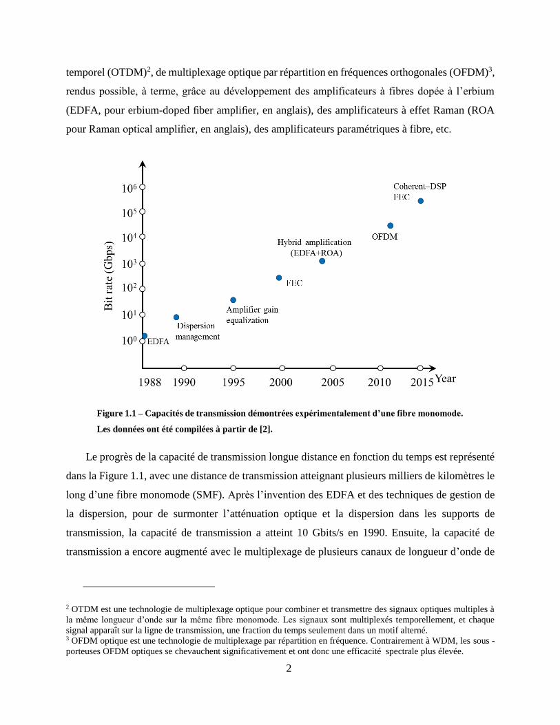
Le progrès de la capacité de transmission longue distance en fonction du temps est représenté
dans la Figure 1.1, avec une distance de transmission atteignant plusieurs milliers de kilomètres le
long d’une fibre monomode (SMF). Après l’invention des EDFA et des techniques de gestion de
la dispersion, pour de surmonter l’atténuation optique et la dispersion dans les supports de
transmission, la capacité de transmission a atteint 10 Gbits/s en 1990. Ensuite, la capacité de
transmission a encore augmenté avec le multiplexage de plusieurs canaux de longueur d’onde de
2 OTDM est une technologie de multiplexage optique pour combiner et transmettre des signaux optiques multiples à
la même longueur d’onde sur la même fibre monomode. Les signaux sont multiplexés temporellement, et chaque
signal apparaît sur la ligne de transmission, une fraction du temps seulement dans un motif alterné. 3 OFDM optique est une technologie de multiplexage par répartition en fréquence. Contrairement à WDM, les sous -
porteuses OFDM optiques se chevauchent significativement et ont donc une efficacité spectrale plus élevée.
3
la bande C ainsi que des bandes L- et S-. Avec l’égalisation du gain, la capacité totale a pu atteindre
40-100 Gbit/s en 1995 [2]. L’exploitation de l’efficacité spectrale serait alors améliorée avec
d’autres travaux de R&D et des démonstrations expérimentales en déployant des canaux sur
l’ensemble de la bande C, puis sur les bandes L et S en utilisant des amplificateurs hybrides (EDFA
+ ROA) pour atteindre 2 Tbit/s au tournant de ce siècle.
Au cours des quinze premières années de ce siècle, nous avons assisté à d’autres progrès ayant
pour put de pousser la limite de capacité de transmission avec les techniques DWDM, OTDM et
OFDM. Cela a été démontré par les réalisations de transmissions de données de 10,2 Tbit/s sur
une seule longueur d’onde [3], en utilisant l’OFDM optique [4] et de 14 Tbit/s (111 Gbit/s × 140
canal de longueur d’onde) de 26 Tbit/s dans une liaison WDM [5]. En raison de cette énorme
capacité de transmission, depuis le début de vingt-et-unième siècle, les systèmes à base de fibre-
fibre ont largement remplacé les systèmes de transmission radio pour les transmissions longue-
distance de données de télécommunication. Ils ont révolutionné les appels téléphoniques longue
distance, la télévision par câble et, plus important encore, l’Internet. La mise en place de l’Internet
à base de fibres optiques a permis d’établir une plateforme de communication à l’échelle mondiale
pour l’ensemble des modes de communication, à savoir les données, la voix et la vidéo, à la fois
pour le contenu temps réel et non-temps réel. L’internet est composé de grandes mailles des
routeurs et des commutateurs électroniques interconnectés à travers des réseaux de fibres optiques
à haute capacité.
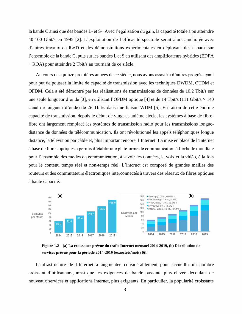
Figure 1.2 – (a) La croissance prévue du trafic Internet mensuel 2014-2019, (b) Distribution de
services prévue pour la période 2014-2019 (exaoctets/mois) [6].
L’infrastructure de l’Internet a augmentée considérablement pour accueillir un nombre
croissant d’utilisateurs, ainsi que les exigences de bande passante plus élevée découlant de
nouveaux services et applications Internet, plus exigeants. En particulier, la popularité croissante
4
des services gourmands en bande passante tels que la diffusion vidéo (Netflix, YouTube, télévision
sur protocole Internet (IPTV)), la vidéophonie (Skype, FaceTime, Google Hangouts), les jeux en
ligne en haute définition (League of legends, Counter-strike, Fallout) et de services de
d’informatique hébergés (cloud computing) ont conduit à une augmentation incessante du trafic
Internet au cours de la dernière décennie - une tendance qui devrait se poursuivre pendant des
années à venir. Selon le Cisco Visual Networking Index (Cisco CVNI), le trafic Internet mondial
a augmenté de plus de quatre fois au cours des cinq dernières années et devrait tripler au cours des
cinq prochaines années (voir la Figure 1.2 (a)) [6]. Parmi les autres services, les services de vidéo
vont dominer la croissance du trafic Internet prédit par le CVNI ( Figure 1.2 (b)). Le trafic Internet
devrait croître à 168 exaoctets par mois en 2019, contre 59,9 exaoctets par mois en 2014, voir
Figure 1.2 (a). Pour apprécier l’ampleur des volumes de trafic Internet, mettons les chiffres en
termes plus familiers: en 2019, le trafic Internet va globalement atteindre 518 térabits par seconde
(Tbit/s). Ceci est l’équivalent de 191 millions de personnes visionnant sur internet une vidéo haute
définition (HD) en même temps, toute la journée, chaque jour, ou l’équivalent de 42 milliards de
DVD par mois.
La capacité susmentionnée fournie par les technologies de transport optique ont toujours été
en avance sur la demande de trafic Internet, et l’accès à la capacité de transmission nécessaire pour
les prochaines années est non loin de la réalisation. Toutefois, la capacité de transmission ne
constitue pas l’ensemble du tableau, mais une partie de celui-ci, comme mentionné précédemment,
l’Internet et, en général, un réseau de communication a essentiellement deux fonctions: la
transmission et le routage/commutation [7]. L’information sous forme de bits binaires est envoyée
à partir d’une origine à une destination finale à travers les canaux de transmission via de nombreux
nœuds de réseau intermédiaires. À ces nœuds, la commutation a lieu de manière à acheminer les
bits à partir de l’origine à la destination le long d’un chemin prédéfinie. L’acheminement (ou le
routage) et la commutation peuvent être réalisés soit dans le domaine électrique ou optique.
La technologie de commutation dans le domaine électrique est mature et très efficace. À ce
jour, la combinaison de transmission optique et de routage électrique fonctionne très bien, comme
en témoigne le fait que jusqu’à présent, dans la plupart des réseaux commerciaux, les informations
sont transmises dans le domaine optique et acheminés dans le domaine électrique. Cependant, le
routage/commutation dans le domaine électrique connaît une pression en constante augmentation
5
à cause de l’augmentation continue des capacités de transmission dans les fibres optiques discutée
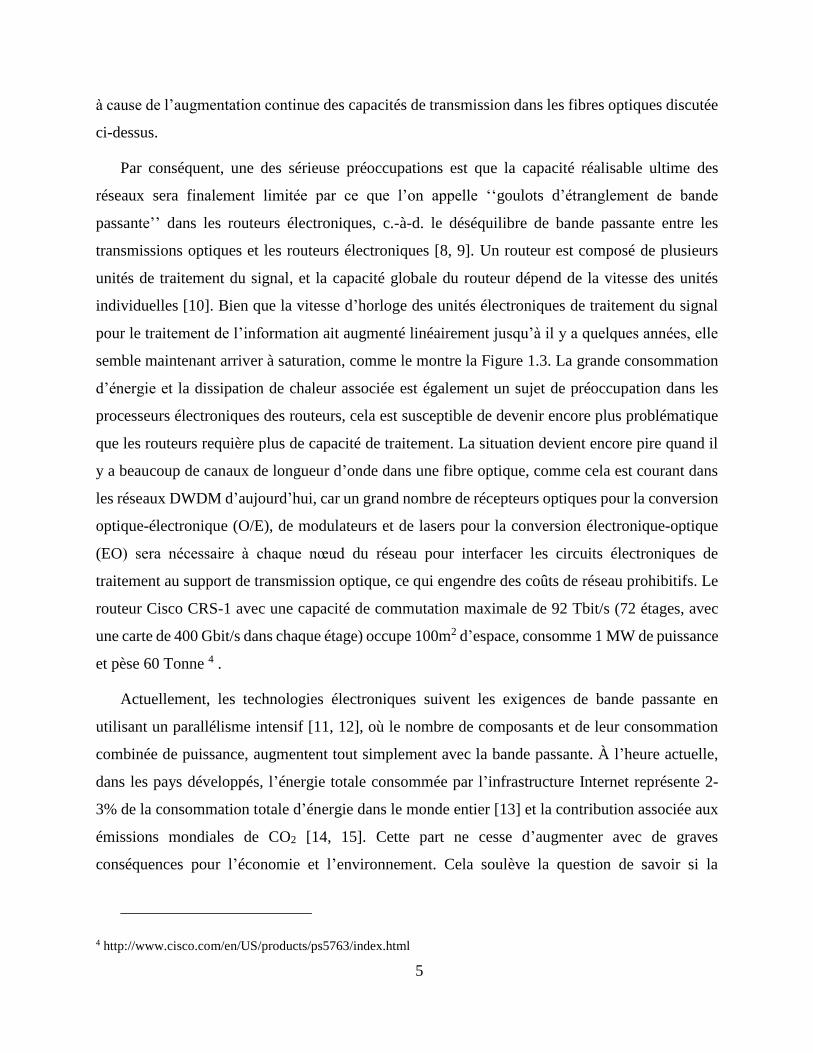
ci-dessus.
Par conséquent, une des sérieuse préoccupations est que la capacité réalisable ultime des
réseaux sera finalement limitée par ce que l’on appelle ‘‘goulots d’étranglement de bande
passante’’ dans les routeurs électroniques, c.-à-d. le déséquilibre de bande passante entre les
transmissions optiques et les routeurs électroniques [8, 9]. Un routeur est composé de plusieurs
unités de traitement du signal, et la capacité globale du routeur dépend de la vitesse des unités
individuelles [10]. Bien que la vitesse d’horloge des unités électroniques de traitement du signal
pour le traitement de l’information ait augmenté linéairement jusqu’à il y a quelques années, elle
semble maintenant arriver à saturation, comme le montre la Figure 1.3. La grande consommation
d’énergie et la dissipation de chaleur associée est également un sujet de préoccupation dans les
processeurs électroniques des routeurs, cela est susceptible de devenir encore plus problématique
que les routeurs requière plus de capacité de traitement. La situation devient encore pire quand il
y a beaucoup de canaux de longueur d’onde dans une fibre optique, comme cela est courant dans
les réseaux DWDM d’aujourd’hui, car un grand nombre de récepteurs optiques pour la conversion
optique-électronique (O/E), de modulateurs et de lasers pour la conversion électronique-optique
(EO) sera nécessaire à chaque nœud du réseau pour interfacer les circuits électroniques de
traitement au support de transmission optique, ce qui engendre des coûts de réseau prohibitifs. Le
routeur Cisco CRS-1 avec une capacité de commutation maximale de 92 Tbit/s (72 étages, avec
une carte de 400 Gbit/s dans chaque étage) occupe 100m2 d’espace, consomme 1 MW de puissance
et pèse 60 Tonne 4 .
Actuellement, les technologies électroniques suivent les exigences de bande passante en
utilisant un parallélisme intensif [11, 12], où le nombre de composants et de leur consommation
combinée de puissance, augmentent tout simplement avec la bande passante. À l’heure actuelle,
dans les pays développés, l’énergie totale consommée par l’infrastructure Internet représente 2-
3% de la consommation totale d’énergie dans le monde entier [13] et la contribution associée aux
émissions mondiales de CO2 [14, 15]. Cette part ne cesse d’augmenter avec de graves
conséquences pour l’économie et l’environnement. Cela soulève la question de savoir si la
4 http://www.cisco.com/en/US/products/ps5763/index.html
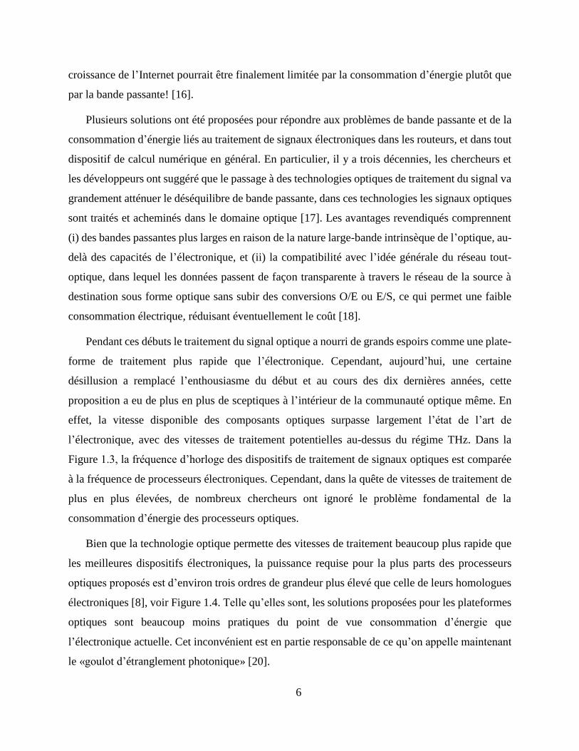
6
croissance de l’Internet pourrait être finalement limitée par la consommation d’énergie plutôt que
par la bande passante! [16].
Plusieurs solutions ont été proposées pour répondre aux problèmes de bande passante et de la
consommation d’énergie liés au traitement de signaux électroniques dans les routeurs, et dans tout
dispositif de calcul numérique en général. En particulier, il y a trois décennies, les chercheurs et
les développeurs ont suggéré que le passage à des technologies optiques de traitement du signal va
grandement atténuer le déséquilibre de bande passante, dans ces technologies les signaux optiques
sont traités et acheminés dans le domaine optique [17]. Les avantages revendiqués comprennent
(i) des bandes passantes plus larges en raison de la nature large-bande intrinsèque de l’optique, au-
delà des capacités de l’électronique, et (ii) la compatibilité avec l’idée générale du réseau tout-
optique, dans lequel les données passent de façon transparente à travers le réseau de la source à
destination sous forme optique sans subir des conversions O/E ou E/S, ce qui permet une faible
consommation électrique, réduisant éventuellement le coût [18].
Pendant ces débuts le traitement du signal optique a nourri de grands espoirs comme une plate-
forme de traitement plus rapide que l’électronique. Cependant, aujourd’hui, une certaine
désillusion a remplacé l’enthousiasme du début et au cours des dix dernières années, cette
proposition a eu de plus en plus de sceptiques à l’intérieur de la communauté optique même. En
effet, la vitesse disponible des composants optiques surpasse largement l’état de l’art de
l’électronique, avec des vitesses de traitement potentielles au-dessus du régime THz. Dans la
Figure 1.3, la fréquence d’horloge des dispositifs de traitement de signaux optiques est comparée
à la fréquence de processeurs électroniques. Cependant, dans la quête de vitesses de traitement de
plus en plus élevées, de nombreux chercheurs ont ignoré le problème fondamental de la
consommation d’énergie des processeurs optiques.
Bien que la technologie optique permette des vitesses de traitement beaucoup plus rapide que
les meilleures dispositifs électroniques, la puissance requise pour la plus parts des processeurs
optiques proposés est d’environ trois ordres de grandeur plus élevé que celle de leurs homologues
électroniques [8], voir Figure 1.4. Telle qu’elles sont, les solutions proposées pour les plateformes
optiques sont beaucoup moins pratiques du point de vue consommation d’énergie que
l’électronique actuelle. Cet inconvénient est en partie responsable de ce qu’on appelle maintenant
le «goulot d’étranglement photonique» [20].
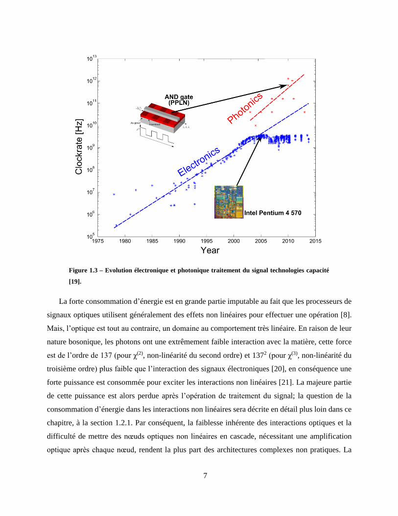
7
Figure 1.3 – Evolution électronique et photonique traitement du signal technologies capacité
[19].
La forte consommation d’énergie est en grande partie imputable au fait que les processeurs de
signaux optiques utilisent généralement des effets non linéaires pour effectuer une opération [8].
Mais, l’optique est tout au contraire, un domaine au comportement très linéaire. En raison de leur
nature bosonique, les photons ont une extrêmement faible interaction avec la matière, cette force
est de l’ordre de 137 (pour χ(2), non-linéarité du second ordre) et 1372 (pour χ(3), non-linéarité du
troisième ordre) plus faible que l’interaction des signaux électroniques [20], en conséquence une
forte puissance est consommée pour exciter les interactions non linéaires [21]. La majeure partie
de cette puissance est alors perdue après l’opération de traitement du signal; la question de la
consommation d’énergie dans les interactions non linéaires sera décrite en détail plus loin dans ce
chapitre, à la section 1.2.1. Par conséquent, la faiblesse inhérente des interactions optiques et la
difficulté de mettre des nœuds optiques non linéaires en cascade, nécessitant une amplification
optique après chaque nœud, rendent la plus part des architectures complexes non pratiques. La
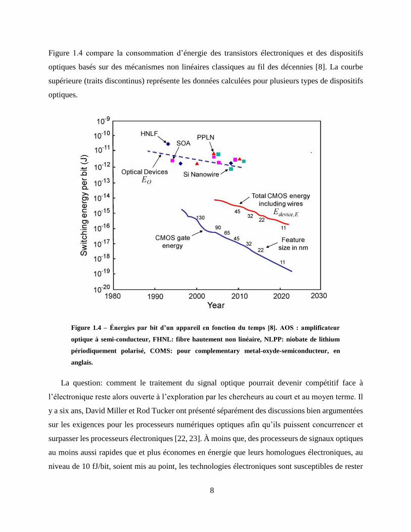
8
Figure 1.4 compare la consommation d’énergie des transistors électroniques et des dispositifs
optiques basés sur des mécanismes non linéaires classiques au fil des décennies [8]. La courbe
supérieure (traits discontinus) représente les données calculées pour plusieurs types de dispositifs
optiques.
Figure 1.4 – Énergies par bit d’un appareil en fonction du temps [8]. AOS : amplificateur
optique à semi-conducteur, FHNL: fibre hautement non linéaire, NLPP: niobate de lithium
périodiquement polarisé, COMS: pour complementary metal-oxyde-semiconducteur, en
anglais.
La question: comment le traitement du signal optique pourrait devenir compétitif face à
l’électronique reste alors ouverte à l’exploration par les chercheurs au court et au moyen terme. Il
y a six ans, David Miller et Rod Tucker ont présenté séparément des discussions bien argumentées
sur les exigences pour les processeurs numériques optiques afin qu’ils puissent concurrencer et
surpasser les processeurs électroniques [22, 23]. À moins que, des processeurs de signaux optiques
au moins aussi rapides que et plus économes en énergie que leurs homologues électroniques, au
niveau de 10 fJ/bit, soient mis au point, les technologies électroniques sont susceptibles de rester
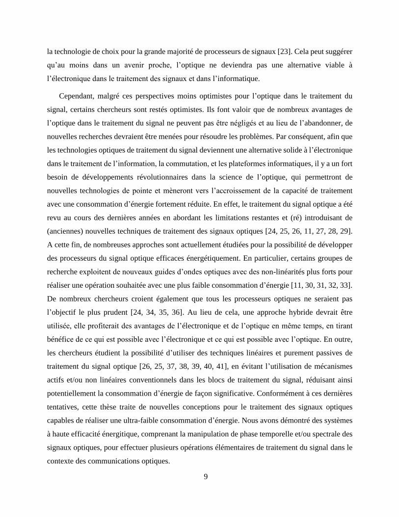
9
la technologie de choix pour la grande majorité de processeurs de signaux [23]. Cela peut suggérer
qu’au moins dans un avenir proche, l’optique ne deviendra pas une alternative viable à
l’électronique dans le traitement des signaux et dans l’informatique.
Cependant, malgré ces perspectives moins optimistes pour l’optique dans le traitement du
signal, certains chercheurs sont restés optimistes. Ils font valoir que de nombreux avantages de
l’optique dans le traitement du signal ne peuvent pas être négligés et au lieu de l’abandonner, de
nouvelles recherches devraient être menées pour résoudre les problèmes. Par conséquent, afin que
les technologies optiques de traitement du signal deviennent une alternative solide à l’électronique
dans le traitement de l’information, la commutation, et les plateformes informatiques, il y a un fort
besoin de développements révolutionnaires dans la science de l’optique, qui permettront de
nouvelles technologies de pointe et mèneront vers l’accroissement de la capacité de traitement
avec une consommation d’énergie fortement réduite. En effet, le traitement du signal optique a été
revu au cours des dernières années en abordant les limitations restantes et (ré) introduisant de
(anciennes) nouvelles techniques de traitement des signaux optiques [24, 25, 26, 11, 27, 28, 29].
A cette fin, de nombreuses approches sont actuellement étudiées pour la possibilité de développer
des processeurs du signal optique efficaces énergétiquement. En particulier, certains groupes de
recherche exploitent de nouveaux guides d’ondes optiques avec des non-linéarités plus forts pour
réaliser une opération souhaitée avec une plus faible consommation d’énergie [11, 30, 31, 32, 33].
De nombreux chercheurs croient également que tous les processeurs optiques ne seraient pas
l’objectif le plus prudent [24, 34, 35, 36]. Au lieu de cela, une approche hybride devrait être
utilisée, elle profiterait des avantages de l’électronique et de l’optique en même temps, en tirant
bénéfice de ce qui est possible avec l’électronique et ce qui est possible avec l’optique. En outre,
les chercheurs étudient la possibilité d’utiliser des techniques linéaires et purement passives de
traitement du signal optique [26, 25, 37, 38, 39, 40, 41], en évitant l’utilisation de mécanismes
actifs et/ou non linéaires conventionnels dans les blocs de traitement du signal, réduisant ainsi
potentiellement la consommation d’énergie de façon significative. Conformément à ces dernières
tentatives, cette thèse traite de nouvelles conceptions pour le traitement des signaux optiques
capables de réaliser une ultra-faible consommation d’énergie. Nous avons démontré des systèmes
à haute efficacité énergitique, comprenant la manipulation de phase temporelle et/ou spectrale des
signaux optiques, pour effectuer plusieurs opérations élémentaires de traitement du signal dans le
contexte des communications optiques.
10
Dans ce chapitre, nous allons d’abord examiner les principes de base des technologies
optiques de traitement du signal en mettant l’accent sur leur performance en matière de
consommation d’énergie. Enfin, nous concluons ce chapitre d’introduction avec un aperçu de l’état
de l’art d’un ensemble particulier de fonctionnalités optiques de traitement du signal de haute
importance pour cette thèse.
1.2 Traitement du signal optique et consommation d’énergie
Le traitement du signal optique est une technologie habilitante qui englobe la théorie
fondamentale, les applications, les algorithmes et les implémentations de traitement ou de transfert
de l’information codée dans une onde lumineuse - le signal optique- dans le domaine temporel
et/ou domaine spatial. L’objectif principal de cette thèse est le traitement du signal optique dans le
domaine temporel, qui est d’un grand intérêt et largement utilisé dans les systèmes de
communication et d’informatique.
Le traitement du signal optique temporel a été le champ d’investigations actives depuis de
nombreuses années, réunissant divers domaines de l’optique et du traitement du signal -à savoir,
les dispositifs et processus linéaires/non-linéaires, l’optique, les signaux analogiques et
numériques- pour réaliser des fonctions de traitement du signal à haute vitesse qui peut
potentiellement fonctionner aux vitesses des signaux à la sortie des fibres optiques de
communications. En particulier, le traitement du signal optique dans le domaine temporel peut
généralement être classés en deux catégories principales: traitement linéaire et non linéaire du
signal, selon les effets optiques (linéaires/ non-linéaire) qu’ils utilisent pour effectuer le traitement
du signal.
Dans le cadre du traitement du signal optique, le traitement linéaire utilise un cadre théorique
riche basé sur la théorie des systèmes linéaires et des transformées de Fourier, largement utilisées
en optique pour la description de la diffraction et du filtrage spatial. Les processeurs de signaux
linéaires exécutent la fonctionnalité ciblée sur le signal optique d’entrée en le déviant, le retardant,
et le filtrant, mais la fréquence reste inchangée et le principe fondamental de superposition est
toujours maintenu. En revanche, l’optique non linéaire, connue comme l’optique de la lumière
intense, est utilisée dans les processeurs optiques qui nécessitent un ou plusieurs faisceaux optiques
pour interagir les uns avec les autres sans interférence [42]. Les faisceaux optiques s’affectent
11
mutuellement et modifient l’amplitude, la phase, la longueur d’onde et polarisation caractéristiques
de chacun d’eux en se propageant à travers le milieu non linéaire et, en conséquence, le principe
de superposition n’est plus valide.
Figure 1.5 – Les applications de traitement de signaux optiques linéaires et non linéaires [43,
44, 45, 46, 47, 48, 49]. Les sujets en noir uni sont abordés dans ce travail et ceux en vert sont
dans les perspectives pour les travaux futurs.
Il existe de nombreuses fonctionnalités qui sont intrinsèquement non linéaires et nous avons
besoin d'un mécanisme non linéaire pour effectuer le traitement du signal associé, telles que la
conversion de la longueur d'onde et la régénération. Cependant, il existe un grand nombre de
fonctionnalités qui sont soit intrinsèquement linéaires, comme la différenciation et l'intégration,
soit nous nous pouvons trouver des façons de les réaliser avec des mécanismes linéaires, tels que
la récupération d'horloge, la conversion de format et les portes logiques, comme représenté dans
l'arborescence dans la Figure 1.5.
Une brève étude des deux types de processeurs de signaux optiques non-linéaires et linéaires
est présentée dans les sections suivantes en mettant l’accent sur leur performance en matière de
consommation d’énergie. Nous concluons que, dans le but de réduire le coût énergétique global
d’un système optique, il est nécessaire d’éviter l’utilisation des mécanismes non linéaires
gourmands en énergie; autant que possible, la fonctionnalité spécifique ciblée doit être réalisée par
des mécanismes linéaires économes en énergie.
12
1.2.1 Traitement non-linéaire du signal optique
La plupart des phénomènes optiques observés dans la vie quotidienne entrent dans la catégorie
de l’optique linéaire qui explique des effets comme la diffraction, la réfraction et les interférences.
Cependant, à des intensités élevées, des interactions complexes peuvent se produire, ces derniers
sont décrits par la théorie de l’optique non linéaire [50, 49, 51]. Plus concrètement, l’optique non
linéaire est l’étude des interactions complexes qui se produisent suite à la modification des
propriétés optiques d’un système de matériaux par la présence d’une lumière intense. Les niveaux
d’intensité lumineuse qui sont nécessaires pour observer des effets optiques non linéaires sont si
élevés qu’ils ne peuvent généralement pas être observés dans les phénomènes de la vie
quotidienne, et ne peuvent être obtenus qu’en utilisant des lasers à ondes continues (CW) intenses
et des lasers pulsés.
Dans un milieu de propagation diélectrique, les interactions linéaires et non linéaires avec la
lumière peuvent être comprises comme une interaction du champ électrique de la lumière avec les
atomes et les molécules constituant le milieu. Les matériaux sont constitués d’atomes comprenant
des particules chargées (par exemple des ions positifs et des électrons) qui sont affectés par les
champs électriques et magnétiques. Les matériaux diélectriques ont une distribution de charge
neutre à l’échelle macroscopique, ils comprennent un nombre égal de charges positives et
négatives à l’échelle atomique (des ions positifs et des électrons). Un champ électrique oscillant
E(t) déplace les charges et exerce une action de séparation entre les charges positives et négatives
(moment dipolaire), modifiant ainsi le moment dipolaire par unité de volume ou la polarisation
P(t) du matériau (t est la variable du temps). À noter qu’aux fréquences visibles / proche
infrarouge, le champ électrique E(t) interagit avec les matériaux diélectriques principalement par
le biais des charges négatives (électrons). Tant que la perturbation de la trajectoire initiale des
charges est faible, le déplacement induit est linéairement proportionnelle à l’amplitude du champ
d’excitation E(t) décrite par
P(t) =ϵ0χ(1)E(t) (1.1)
où la constante de proportionnalité χ(1) est la susceptibilité linéaire et ɛ0 est la permittivité de
l’espace libre. Des déformations plus fortes des distributions de charge peuvent conduire à rompre
13
cette relation proportionnelle et la réponse optique, la polarisation P(t), est alors exprimée par une
série de puissance de la force du champ E(t) comme suit
P(t) =ϵ0[ χ(1)E(t) + χ(2)E2(t) + χ(3)E3(t) +…] (1.2)
Les quantités χ(2) et χ (3) sont connus comme les susceptibilités optiques non linéaires de
deuxième et de troisième ordre, respectivement. Pour plus de simplicité, nous avons pris les
champs P(t) et E(t) comme des grandeurs scalaires. Nous avons également supposé que la
polarisation à l’ instant t ne dépendrait que de la valeur instantanée de la force du champ électrique,
ce qui implique (à travers les relations de Kramers-Kronig) que le milieu doit être sans perte et
sans dispersion. Nous appelons P(2)(t) = ϵ0 χ(2)E2(t) la polarisation non linéaire de second ordre et
P(3)(t) = ϵ0 χ(3)E3(t) la polarisation non linéaire de troisième ordre. Les interactions optiques non
linéaires de deuxième ordre ne peuvent se produire que dans des cristaux non-centrosymétrique
tels que le Quartz et le Niobate de lithium (LiNbO3), c.-à-d., dans les cristaux qui ne présentent
pas une symétrie d’inversion. Dans des matériaux comme les liquides, les gaz, les solides
amorphes (comme le verre), et même un grand nombre de cristaux présentent une symétrie
d’inversion, χ(2) est nul, et par conséquent de tels matériaux ne peuvent pas produire des
interactions optiques non linéaires de deuxième ordre. Cependant, les interactions optiques non
linéaires de troisième ordre (c.-à-d., ceux qui sont décrits par la susceptibilité χ(3)) peuvent se
produire dans de tels milieux centrosymétriques.
De nos jours, l’application de l’optique non linéaire dans le cadre des sciences de l’information
a deux motivations principales. Les effets non linéaires sont nécessaires pour la création d’une
base pour le traitement des signaux optiques, tandis que d’autre part, ils provoquent des
déformations préjudiciables aux signaux de communication dans les fibres optiques longue
distance. Par conséquent, les applications de traitement du signal, nécessitent un milieu de
propagation avec des effets non linéaires plus élevés pour faciliter le traitement de signal optique
à moindre coût en énergie. À l’opposé, pour la transmission de signaux optiques, on cherche à
minimiser l’effet des non-linéarités du milieu de propagation pour augmenter la capacité de
transmission. Dans le contexte du traitement des signaux optiques, les techniques optiques utilisent
une large gamme de dispositifs non-linéaires avec différents mécanismes pour réaliser de multiples
14
fonctionnalités de réseau. Parmi les technologies de traitement tout-optique nous citons celles
présentant un intérêt significatif pour ce trvail
Les amplificateurs optiques à semiconducteurs (AOS) utilisant χ(3) pour exciter les effets
non-linéaires suivant: la modulation croisée du gain (XGM), l’auto-modulation de phase
(SPM pour self-phase modulation), la modulation croisée de phase (XPM), et le mélange
à quatre ondes (FWM pour four-wave-mixing) [52, 53].
Les fibres fortement non linéaires (HNLF pour Highly Nonlinear Fibers) [54, 55, 56,
57] ou d’autres guides d’ondes (de verre de chalcogénure [58], le silicium sur isolant
(SOI) [59], et semiconducteurs III-V [60, 61]) utilisant χ (3) pour exciter effets non
linéaires SPM, XPM, FWM.
Niobate de lithium polarisé périodiquement (PPLN pour Periodically Poled Lithium
Niobate, en anglais) en utilisant χ(2) pour exciter l’effet non linéaire de mélange à trois
ondes (TWM pour three wave mixing en anglais) [62, 63, 64].
Toutes ces plates-formes ont été largement exploitées, permettant de mettre en œuvre des
portes logiques toutes-optiques [55], la conversion de longueur d’onde [43], la régénération [44],
la génération de peigne de fréquence [45], etc. Elles présentent des réponses optiques picoseconde
et sous-picoseconde et par conséquent, peut potentiellement mener à la réalisation des dispositifs
optiques avec une dynamique beaucoup plus rapide que celle des appareils électroniques actuels.
Mais une vitesse de traitement élevé ne suffit pas à elle seule pour obtenir des systèmes optiques
fiables de haute capacité. La consommation d’énergie du dispositif est au moins aussi
importante [8]. Comme de fortes intensités de lumière sont nécessaires pour stimuler les effets non
linéaires, les dispositifs à base de matériaux non linéaires consomment beaucoup d’énergie. Pour
mieux comprendre les mécanismes de base derrière la consommation d’énergie dans les dispositifs
optiques non linéaires, nous devons tenir compte des processus de transformation de l’énergie au
niveau de l’appareil ou du circuit. La Figure 1.6 montre un schéma bloc d’un dispositif (ou circuit)
de traitement du signal optique basé sur des mécanismes non linéaires. Le circuit est constitué d’un
milieu non linéaire, tel que les SOA, HNLFs ou PPLNs. Typiquement, le dispositif ou le circuit
aura deux ou plusieurs entrées de signal ( la Figure 1.6 montre toutes les entrées considérés comme
entrées de l’informations) et une ou plusieurs sorties de signal ( la Figure 1.6 montre toutes les
sorties considérées comme sortie de L’informations). La Figure 1.6 représente également une
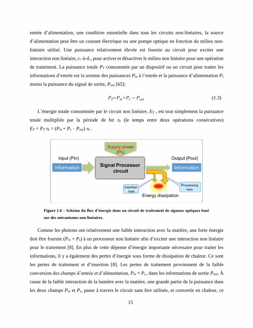
15
entrée d’alimentation, une condition essentielle dans tous les circuits non-linéaires, la source
d’alimentation peut être un courant électrique ou une pompe optique en fonction du milieu non-
linéaire utilisé. Une puissance relativement élevée est fournie au circuit pour exciter une
interaction non linéaire, c.-à-d., pour activer et désactiver le milieu non linéaire pour une opération
de traitement. La puissance totale PT consommée par un dispositif ou un circuit pour traiter les
informations d’entrée est la somme des puissances Pin à l’entrée et la puissance d’alimentation Ps
moins la puissance du signal de sortie, Pout [65]:
PT=Pin+Ps − Pout (1.3)
L’énergie totale consommée par le circuit non linéaire, ET , est tout simplement la puissance
totale multipliée par la période de bit τb (le temps entre deux opérations consécutives)
ET = PT τb = (Pin + Ps – Pout) τb .
Figure 1.6 – Schéma du flux d’énergie dans un circuit de traitement de signaux optiques basé
sur des mécanismes non linéaires.
Comme les photons ont relativement une faible interaction avec la matière, une forte énergie
doit être fournie (Pin + Ps) à un processeur non linéaire afin d’exciter une interaction non linéaire
pour le traitement [8]. En plus de cette dépense d’énergie importante nécessaire pour traiter les
informations, il y a également des pertes d’énergie sous forme de dissipation de chaleur. Ce sont
les pertes de traitement et d’insertion [8]. Les pertes de traitement proviennent de la faible
conversion des champs d’entrée et d’alimentation, Pin + Ps , dans les informations de sortie Pout. À
cause de la faible interaction de la lumière avec la matière, une grande partie de la puissance dans
les deux champs Pin et Ps, passe à travers le circuit sans être utilisée, et convertie en chaleur, ce
16
qui résulte en une faible Pout (Pin +Ps >> Pout signifie un grand ET). Les pertes d’insertion
proviennent de l’absorption et la diffraction de la lumière quand elle se propage à travers le circuit,
car un dispositif optique ne peut pas passer 100% d’une onde lumineuse. En outre, le traitement
du signal optique utilisant des interactions non linéaires nécessite, en général, un
approvisionnement continu d’énergie, indépendamment du fait que ce dispositif exécute ou non
une opération de traitement [8].
En plus des problèmes d’énergie, le degré élevé de contrôle requis sur les caractéristiques
des signaux d’entrée (par exemple, la puissance, la fréquence centrale, état de polarisation, etc.)
impliqués dans une opération non linéaire de traitement a empêché l’application du traitement du
signal optique non linéaire au-delà de l’environnement bien contrôlé de laboratoire. Un
inconvénient supplémentaire des techniques d’optiques non linéaires est que des fibres fortement
non linéaires ou des guides d’ondes à profils de dispersion personnalisés sont nécessaires pour un
traitement efficace, rendant le système coûteux. En outre, la mise en œuvre de systèmes plus
complexes reposant sur la concaténation de deux ou plusieurs processeurs non linéaires du signal
optique pourrait dégrader sensiblement la qualité du signal. Cette dégradation peut être provoquée
par la réduction du rapport signal sur bruit (associée à la faible efficacité énergétique de ces
processeurs, et l’exigence d’amplification supplémentaire), et/ou par l’introduction de
composantes de fréquence parasites dans la bande passante du signal d’information.
1.2.2 Traitement linéaire du signal optique
Les systèmes linéaires peuvent être utilisés pour modéliser et analyser un large éventail de
problèmes dans les domaines de la science et de l’ingénierie. En particulier, les filtres optiques
linéaires ont été largement étudiés, ces dispositifs occupent une position d’une importance
fondamentale dans l’optique spatiale et temporelle [41, 66, 67]. Le traitement linéaire du signal
optique est basé sur la riche théorie des systèmes linéaires et dans de nombreuses applications, les
méthodes de traitement linéaires se révèlent optimales; deux exemples seront présentés dans la
section 1.3. En outre, les méthodes linéaires sont intrinsèquement simples à mettre en œuvre, ce
qui est probablement la raison de leur utilisation généralisée dans la pratique.
Un processeur est dit linéaire si la fonction de transfert, à savoir y = f (x), la fonction définissant
la relation entre les signaux d’entrée et de sortie (x et y respectivement), satisfait au principe de
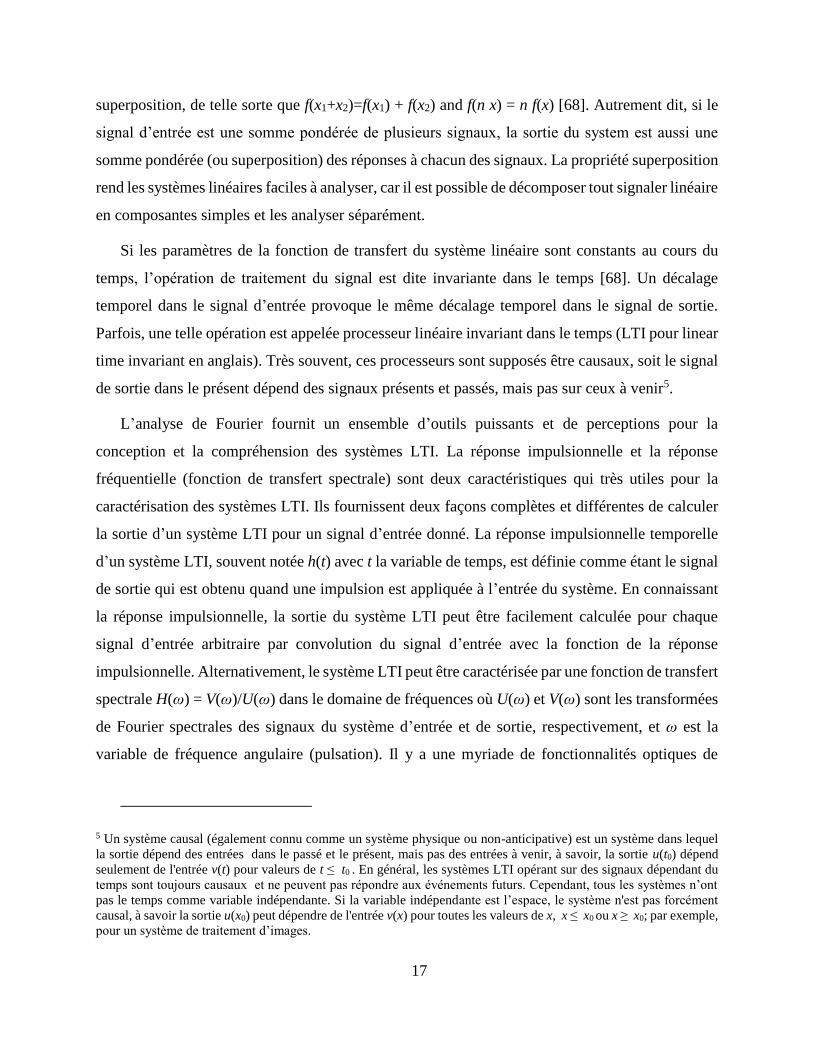
17
superposition, de telle sorte que f(x1+x2)=f(x1) + f(x2) and f(n x) = n f(x) [68]. Autrement dit, si le
signal d’entrée est une somme pondérée de plusieurs signaux, la sortie du system est aussi une
somme pondérée (ou superposition) des réponses à chacun des signaux. La propriété superposition
rend les systèmes linéaires faciles à analyser, car il est possible de décomposer tout signaler linéaire
en composantes simples et les analyser séparément.
Si les paramètres de la fonction de transfert du système linéaire sont constants au cours du
temps, l’opération de traitement du signal est dite invariante dans le temps [68]. Un décalage
temporel dans le signal d’entrée provoque le même décalage temporel dans le signal de sortie.
Parfois, une telle opération est appelée processeur linéaire invariant dans le temps (LTI pour linear
time invariant en anglais). Très souvent, ces processeurs sont supposés être causaux, soit le signal
de sortie dans le présent dépend des signaux présents et passés, mais pas sur ceux à venir5.
L’analyse de Fourier fournit un ensemble d’outils puissants et de perceptions pour la
conception et la compréhension des systèmes LTI. La réponse impulsionnelle et la réponse
fréquentielle (fonction de transfert spectrale) sont deux caractéristiques qui très utiles pour la
caractérisation des systèmes LTI. Ils fournissent deux façons complètes et différentes de calculer
la sortie d’un système LTI pour un signal d’entrée donné. La réponse impulsionnelle temporelle
d’un système LTI, souvent notée h(t) avec t la variable de temps, est définie comme étant le signal
de sortie qui est obtenu quand une impulsion est appliquée à l’entrée du système. En connaissant
la réponse impulsionnelle, la sortie du système LTI peut être facilement calculée pour chaque
signal d’entrée arbitraire par convolution du signal d’entrée avec la fonction de la réponse
impulsionnelle. Alternativement, le système LTI peut être caractérisée par une fonction de transfert
spectrale H(ω) = V(ω)/U(ω) dans le domaine de fréquences où U(ω) et V(ω) sont les transformées
de Fourier spectrales des signaux du système d’entrée et de sortie, respectivement, et ω est la
variable de fréquence angulaire (pulsation). Il y a une myriade de fonctionnalités optiques de
5 Un système causal (également connu comme un système physique ou non-anticipative) est un système dans lequel
la sortie dépend des entrées dans le passé et le présent, mais pas des entrées à venir, à savoir, la sortie u(t0) dépend
seulement de l'entrée v(t) pour valeurs de t ≤ t0 . En général, les systèmes LTI opérant sur des signaux dépendant du
temps sont toujours causaux et ne peuvent pas répondre aux événements futurs. Cependant, tous les systèmes n’ont
pas le temps comme variable indépendante. Si la variable indépendante est l’espace, le système n'est pas forcément
causal, à savoir la sortie u(x0) peut dépendre de l'entrée v(x) pour toutes les valeurs de x, x ≤ x0 ou x ≥ x0; par exemple,
pour un système de traitement d’images.
18
traitement de signaux qui peuvent être décrites par la réponse d’un système LTI, voir Figure 1.5,
telles que les techniques optiques de récupération d’horloge, la mise en forme d’impulsions
optiques, différentiateurs/intégrateurs optiques, et les transformateurs d’impulsions tels que les
transformateurs de Hilbert, entre plusieurs autres applications.
En général, il existe deux procédures principales pour mettre en œuvre des processeurs de
signaux optiques, (i) la conception des filtres spectrales linéaires, tels que résonateurs en anneau,
interféromètres ou des réseaux à fibre, où l’opération de filtrage est réalisée en modifiant
directement le spectre du signal d’entrée (Figure 1.7, à gauche); (ii) le développement des filtres
temporels équivalents aux filtres spatiaux6. Dans les filtres temporels l’opération de filtrage est
réalisée dans le domaine temporel via des processus de modulation (Figure 1.7, à droite). Il
convient de noter que développement des filtres optiques temporels équivalents aux filtres optiques
spatiaux ont été réalisés grâce à ce qui est appelé la dualité espace-temps dans l’optique, qui sera
défini en détail dans le Chapitre 2. L’utilisation de cette dualité, permet d’appliques des techniques
spatiales très efficaces de traitement de l’information optiques sur des signaux temporels, ce qui
rend au final des approches plus sophistiquées et puissantes accessible aux applications de
transformation et de caractérisation de l’information temporelle [69]. Plus particulièrement, une
telle approche a permis le développement de la notion de la lentille-temporelle [69], l’imagerie
temporelle / systèmes d’auto-imagerie [41], le filtrage et la transformation de Fourier optiques en
temps réel [69], etc.
La modulation temporelle linéaire et les processus de filtrage spectral, à leur tour peuvent être
scindés en deux catégories: modulation/filtrage de phase et d’amplitude. La manipulation désirée
du signal peut être produite sur le profil temporel (ou spectrale) d’amplitude ou de phase du signal
sous test par la modulation (filtrage) temporelle (ou spectrale) d’intensité ou de phase, comme le
montre la Figure 1.7.
Un filtre optique d’amplitude spectrale ayant une fonction de transfert H(ω) = A(ω) exp[jϕ(ω)],
où A(ω) et ϕ(ω) désignent les profils d’amplitude et de phase du filtre, respectivement, modifie le
6 Dans le traitement en domaine spatial, l’information est codée dans la distribution spatiale de la lumière, qui se
propage dans l’espace libre. Le traitement de l'information optique spatiale est effectué en utilisant des optiques en
espace libre [67], ce qui implique l'utilisation de lentilles optiques, des réseaux de diffraction, des modulateurs spatiaux
de lumière, etc.
19
contenu spectral du signal d’entrée, et le traitement du signal est typiquement effectuée en
atténuant et/ou en supprimant une partie des composantes spectrales du signal d’entrée (Figure 1.7
, à gauche, en haut). On notera que dans ce type de filtres, si ϕ(ω) = 0, le filtre est dit filtre idéal
d’amplitude-seule, ayant une réponse impulsionnelle pair et non-causale. Dans la pratique
cependant, une phase spectrale linéaire ϕ(ω) = ω t0 est typiquement introduite pour satisfaire la
causalité. Cette variation de phase correspond seulement à un retard temporel de t0, elle n'a donc
pas d’incidence sur la définition du filtre d'amplitude et ne réalise aucune autre transformation sur
le signal d'entrée. Un exemple de filtres d’amplitude typiques comprennent les résonateurs en
anneau [70, 48, 71], les interféromètres [72, 47] ou les structures périodiques comme les réseaux
de fibre ou de guide d’ondes [73, 74]. D’autre part, un filtre optique spectrale de phase-seule
(passe-tout) est caractérisé par une réponse en fréquence H(ω) = A exp [jϕ(ω)], où A est une
amplitude constante, indépendamment de la variable de fréquence. Par conséquent, le filtre
spectral de phase-seule fait passer toutes les composantes spectrales avec une amplitude égale;
alors, si la fonction de transfert d’amplitude spectrale uniforme est conçue pour une transmission
de 100%, fondamentalement aucune énergie de signal n’est perdue dans le procédé (Figure 1.7 , à
gauche, en bas). Au lieu de cela, le filtre de phase décale les composantes spectrales pour effectuer
le traitement du signal voulu. En règle générale, l’intuition des effets temporels induits par
l’amplitude de la réponse en fréquence d’un filtre sur un signal entrant est assez bien développée,
mais en revanche, la visualisation de l’effet de la phase de la réponse en fréquence du signal est
plus subtile, mais tout aussi importante. Un milieu dispersif, tel qu’une fibre optique monomode
classique, est un exemple d’un filtre de phase-seule [41].
De même, les modulateurs d’intensité optique temporelle avec une fonction de modulation
p(t) = A(t) atténuent ou éliminent certaines composantes temporelles du signal d’entrée pour
produire le signal de sortie ciblé, voir Figure 1.7, droite, haut. En revanche, comme le montre la
Figure 1.7, à droite, en bas, un modulateur de phase temporelle avec fonction de modulation de
p(t) = exp[ jϕ(t)] ne modifie que la phase de l’onde lumineuse qui le traverse et, en substance,
aucune énergie n’est perdue dans le processus.
20
Figure 1.7 – Procédures de mise en œuvre de la modulation temporelle et du filtrage spectral
linéaires.
Il convient de noter que les filtres spectraux sont des composants passifs, c.-à-d., ils ne
nécessitent pas une source externe d’énergie pour accomplir leurs fonctionnalités. Cependant, les
modulateurs temporels sont des composants actifs, qui nécessitent une source d’énergie externe
pour fonctionner et remplir les fonctions ciblées. Dans cette thèse, chaque fois que possible, nous
utilisons des techniques de filtrage spectral linéaires passives et économes en énergie pour réaliser
une fonctionnalité spécifique. Néanmoins, toutes les fonctionnalités ne peuvent être mises en
œuvre en utilisant uniquement des systèmes passifs et dans de nombreux cas, nous avons besoin
d’incorporer des techniques linéaires de modulation temporelles actives. Les mécanismes de
modulation temporelle d’un signal optique les plus simples et les plus économes en énergie
peuvent être réalisés grâce aux systèmes de modulation électro-optique. Dans ces systèmes, le
signal de modulation est un signal électronique, qui a intrinsèquement une énergie inférieure à
celle du signal optique. Plus important encore, l’effet de modulation électro-optique est induit en
utilisant une non-linéarité du second ordre, ce qui nécessite typiquement beaucoup moins d’énergie
provenant de la source de modulation comparé à la modulation tout-optique qui utilise la non-
linéarité de troisième ordre.
La Figure 1.8 illustre la transformation de l’énergie qui a lieu dans les méthodes de
modulation/filtrage linéaires d’amplitude et de phase. L’énergie de l’information de sortie provient
entièrement de l’énergie de l’information d’entrée dans tous les procédés.
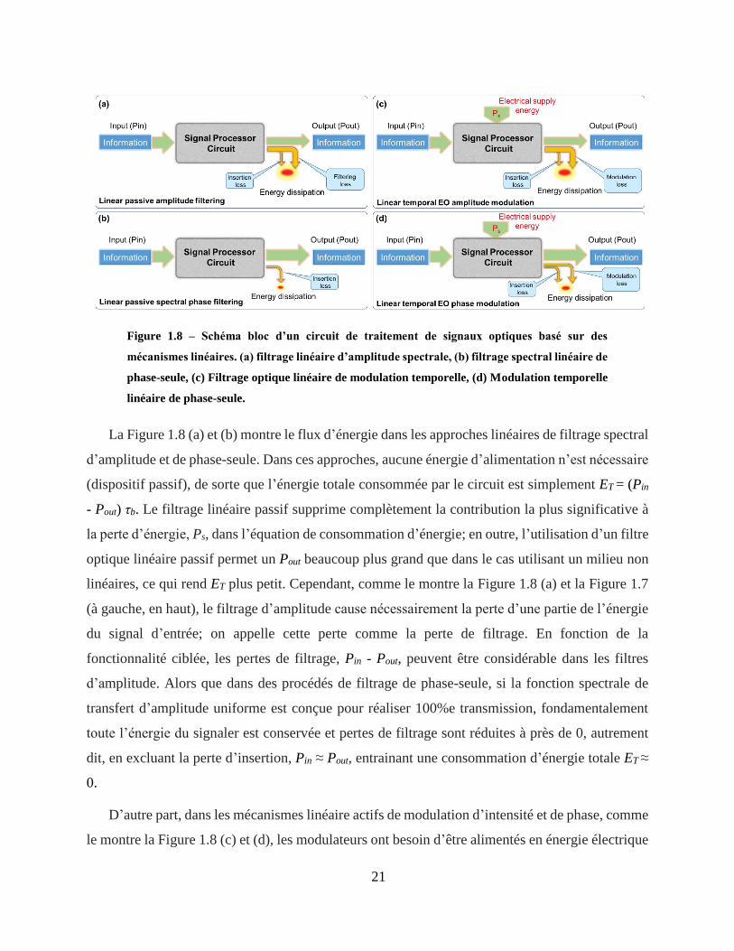
21
Figure 1.8 – Schéma bloc d’un circuit de traitement de signaux optiques basé sur des
mécanismes linéaires. (a) filtrage linéaire d’amplitude spectrale, (b) filtrage spectral linéaire de
phase-seule, (c) Filtrage optique linéaire de modulation temporelle, (d) Modulation temporelle
linéaire de phase-seule.
La Figure 1.8 (a) et (b) montre le flux d’énergie dans les approches linéaires de filtrage spectral
d’amplitude et de phase-seule. Dans ces approches, aucune énergie d’alimentation n’est nécessaire
(dispositif passif), de sorte que l’énergie totale consommée par le circuit est simplement ET = (Pin
- Pout) τb. Le filtrage linéaire passif supprime complètement la contribution la plus significative à
la perte d’énergie, Ps, dans l’équation de consommation d’énergie; en outre, l’utilisation d’un filtre
optique linéaire passif permet un Pout beaucoup plus grand que dans le cas utilisant un milieu non
linéaires, ce qui rend ET plus petit. Cependant, comme le montre la Figure 1.8 (a) et la Figure 1.7
(à gauche, en haut), le filtrage d’amplitude cause nécessairement la perte d’une partie de l’énergie
du signal d’entrée; on appelle cette perte comme la perte de filtrage. En fonction de la
fonctionnalité ciblée, les pertes de filtrage, Pin - Pout, peuvent être considérable dans les filtres
d’amplitude. Alors que dans des procédés de filtrage de phase-seule, si la fonction spectrale de
transfert d’amplitude uniforme est conçue pour réaliser 100%e transmission, fondamentalement
toute l’énergie du signaler est conservée et pertes de filtrage sont réduites à près de 0, autrement
dit, en excluant la perte d’insertion, Pin ≈ Pout, entrainant une consommation d’énergie totale ET ≈
0.
D’autre part, dans les mécanismes linéaire actifs de modulation d’intensité et de phase, comme
le montre la Figure 1.8 (c) et (d), les modulateurs ont besoin d’être alimentés en énergie électrique
22
(Ps) afin d’exciter l’interaction non linéaire du second ordre, l’énergie totale consommée par les
modulateurs est alors ET = (Pin + Ps - Pout) τb. Dans ces mécanismes, l’énergie d’alimentation ne
contribue pas directement à l’énergie de sortie porteuse d’informations, c.-à-d., l’énergie du signal
d’information de sortie, Pout, provient entièrement de l’énergie de l’information d’entrée, Pin, (i.e.,
Pout ≤ Pin). Par conséquent, l’énergie d’alimentation Ps est entièrement dissipée dans le dispositif,
après avoir permis de réaliser la modification désirée dans les caractéristiques de phase du signal
d’entrée. Cependant, la quantité d’énergie d’alimentation électrique, Ps, est nettement inférieure à
celle des dispositifs optiques non linéaires, où un signal optique est utilisé comme l'énergie
d'alimentation pour exciter un effet non linéaire dans le milieu non linéaire représentés sur la
Figure 1.6, ce qui rend l’énergie consommée ET plus faible dans les mécanismes de modulation
électro-optique. Il importe de mentionner que dans la modulation EO d'amplitude temporel, en
plus de l'alimentation en tension de modulation, nous avons également besoin d' une alimentation
en tension de polarisation qui rend la puissance d'alimentation totale, Ps, dans ce procédé plus
grande que celle de la modulation de phase EO.
D’une manière générale, les pertes de modulation désignent la quantité d’énergie qui est perdue
à partir de la puissance d’entrée dans le processus de modulation, Pin - Pout. Les pertes de
modulation excluent la contribution des pertes d’insertion. Comme mentionné plus haut, comme
dans le filtrage d’amplitude, la modulation d’intensité cause également une perte d’une partie de
l’énergie du signal d’entrée, cela est montré dans la Figure 1.8 (c) et la Figure 1.7 (gauche, bas).
Par conséquent, l’énergie perdue de la puissance d’entrée, Pin - Pout, peut être considérable dans
un procédé de modulation d’intensité. À l’inverse de cela, l’énergie du signal peut être entièrement
préservée si seule la phase du signal est manipulée dans le domaine temporel par la modulation de
phase temporelle. Par conséquent, la majeure partie de la lumière passe à travers les dispositifs de
modulation de phase, assurant ainsi une plus faible consommation d’énergie, pratiquement
Pin ≈ Pout et la consommation totale d’énergie sera alors déterminée par l’énergie d’alimentation
externe, ET = Ps τb.
Afin de fournir un exemple quantitatif de consommation d'énergie dans la modulation de phase
temporelle d'un signal d'entrée, nous estimons la consommation d'énergie dans le processus de
modulation de phase électro-optique et le procédé de modulation en phase croisée (XPM) pour
induire un effet d'auto-imagerie spectrale [75] (qui sera adressé dans le chapitre suivant) sur un

23
train d'impulsions optiques périodiques (avec une période temporelle de 100ps), comme le montre
la Figure 1.9 . Dans notre estimation, nous prenons en compte un HNLF avec un coefficient non-
linéaire (d’effet Kerr) γ= 11 W-1Km-1 et un modulateur de phase électro-optique avec Vπ = 3.0 V.
Ces spécifications correspondent aux valeurs conventionnelles pour les deux processus évalués,
selon l’état actuel de la technologique. La consommation d'énergie estimée est de ET = Ps τb =
125mW× 100ps = 12.5 pJ/période pour le processus de modulation de phase en utilisant la XPM
[76], et il est de ET = Ps τb = Vπ
2
8 R τb = 22.5mW× 100ps = 2.25 pJ/période, où R = 50Ω est la résistance
du modulateur, pour la modulation électro-optique [77]. En plus de l'amélioration de la
performance énergétique par un facteur cinq, la modulation électro-optique fournit également le
mécanisme le plus simple de modulation de phase temporelle.
L’utilisation de l’optique linéaire permet une consommation d’énergie beaucoup plus faible
que dans le cas utilisant les mécanismes non-linéaires. Par conséquent, afin de réduire le budget
énergétique global d’un système de traitement du signal optique, il est nécessaire d’éviter
l’utilisation des mécanismes non linéaires gourmands en énergie, et de mettre en œuvre les
fonctionnalités spécifiques souhaitées à l’aide des mécanismes linéaires économes en énergie.
Figure 1.9 – Traitement d'un train périodique d'impulsions optiques d'entrée (Pin(t)) en
utilisant (a) la modulation non linéaire de phase croisée (XPM) et (b) l'effet électro-optique.
24
1.3 Revu des processeurs de signaux optiques pertinents étudiés dans
cette thèse
Parmi les fonctions de traitement du signal d’importance critique étudiées dans cette thèse nous
citons: la récupération d’horloge (RH) tout-optique, la conversion de format optique et le contrôle
du taux de répétition des lasers impulsionnels pour des applications de télécommunications. Dans
cette section, nous passons en revue de manière courte et non-exhaustive les quelques-unes des
méthodes démontrées précédemment. Le but de cette discussion est de mettre notre travail en
contexte.
1.3.1 Récupération de l’horloge optique
Au cours des 20 dernières années, une grande variété de méthodes optiques de récupération
des signaux d’horloge "de base" et "sous-harmonique" basées sur différents principes physiques
ont été proposées et démontrées [78, 79, 46, 80, 81, 82, 83, 84, 85]. La RH est une opération
fondamentale effectuée dans tous les appareils numériques de communication allant des
téléphones mobiles ordinaires à des récepteurs optiques à grande vitesse. Dans les
télécommunications optiques, l’horloge est traditionnellement récupérée par des circuits
électroniques. Pour un récepteur classique qui convertit le signal optique en un signal électrique,
le RH électronique est un choix naturel. Il existe, cependant, des emplacements et des dispositifs
dans l’architecture des réseaux optiques, où la conversion optique-électrique n’est pas nécessaire.
Le choix préféré serait alors de maintenir le signal dans le domaine optique. Des exemples de tels
dispositifs sont, les régénérateurs de signaux tout-optique [44], les(dé)multiplexeurs par division
temporelle [17], les portes logiques optiques [55], ou, en général, les points dans le réseau où le
signal transmis doit être (re)synchronisé mais pas terminé. Tous les systèmes de
télécommunications numériques se composent de trois principaux éléments: un émetteur, un
chemin de transmission, et un récepteur. L’émetteur et le récepteur sont généralement séparés par
une distance considérable, donc le récepteur n’a aucun moyen d’obtenir des informations directes
sur l’horloge de l’émetteur. Naturellement, les informations d’horloge pourraient être envoyées à
travers un canal de communication séparé menant à la réduction de la bande passante nette et
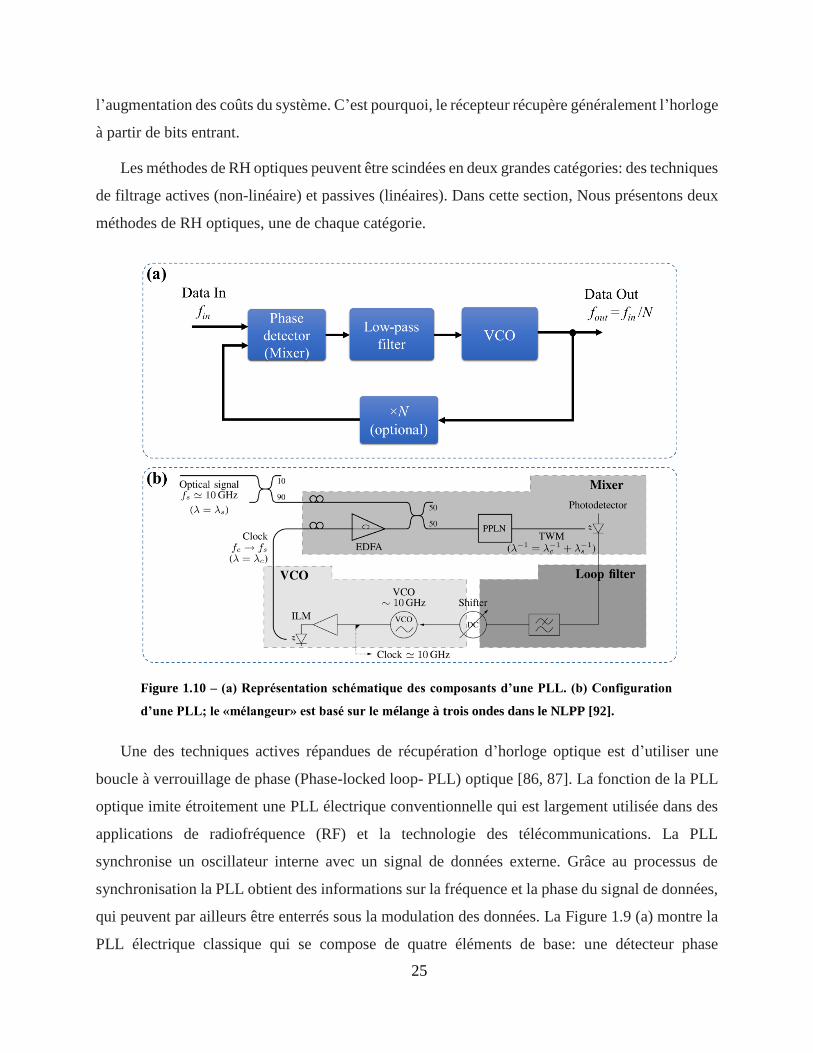
25
l’augmentation des coûts du système. C’est pourquoi, le récepteur récupère généralement l’horloge
à partir de bits entrant.
Les méthodes de RH optiques peuvent être scindées en deux grandes catégories: des techniques
de filtrage actives (non-linéaire) et passives (linéaires). Dans cette section, Nous présentons deux
méthodes de RH optiques, une de chaque catégorie.
Figure 1.10 – (a) Représentation schématique des composants d’une PLL. (b) Configuration
d’une PLL; le «mélangeur» est basé sur le mélange à trois ondes dans le NLPP [92].
Une des techniques actives répandues de récupération d’horloge optique est d’utiliser une
boucle à verrouillage de phase (Phase-locked loop- PLL) optique [86, 87]. La fonction de la PLL
optique imite étroitement une PLL électrique conventionnelle qui est largement utilisée dans des
applications de radiofréquence (RF) et la technologie des télécommunications. La PLL
synchronise un oscillateur interne avec un signal de données externe. Grâce au processus de
synchronisation la PLL obtient des informations sur la fréquence et la phase du signal de données,
qui peuvent par ailleurs être enterrés sous la modulation des données. La Figure 1.9 (a) montre la
PLL électrique classique qui se compose de quatre éléments de base: une détecteur phase
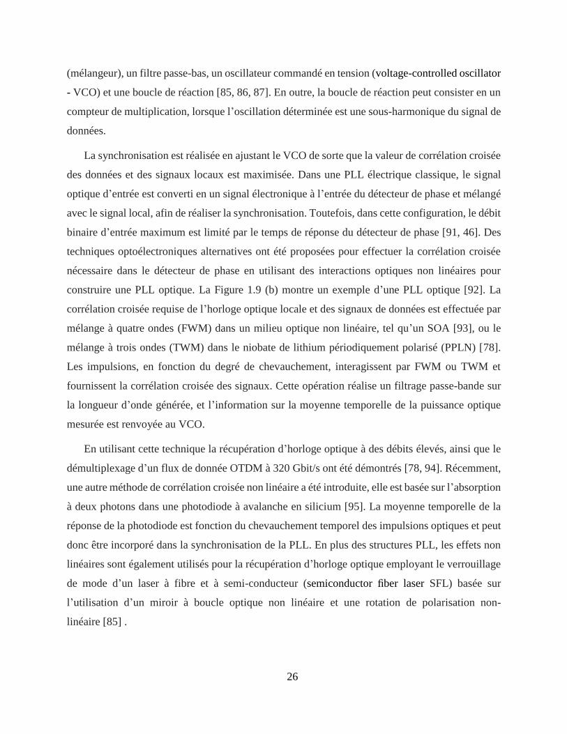
26
(mélangeur), un filtre passe-bas, un oscillateur commandé en tension (voltage-controlled oscillator
- VCO) et une boucle de réaction [85, 86, 87]. En outre, la boucle de réaction peut consister en un
compteur de multiplication, lorsque l’oscillation déterminée est une sous-harmonique du signal de
données.
La synchronisation est réalisée en ajustant le VCO de sorte que la valeur de corrélation croisée
des données et des signaux locaux est maximisée. Dans une PLL électrique classique, le signal
optique d’entrée est converti en un signal électronique à l’entrée du détecteur de phase et mélangé
avec le signal local, afin de réaliser la synchronisation. Toutefois, dans cette configuration, le débit
binaire d’entrée maximum est limité par le temps de réponse du détecteur de phase [91, 46]. Des
techniques optoélectroniques alternatives ont été proposées pour effectuer la corrélation croisée
nécessaire dans le détecteur de phase en utilisant des interactions optiques non linéaires pour
construire une PLL optique. La Figure 1.9 (b) montre un exemple d’une PLL optique [92]. La
corrélation croisée requise de l’horloge optique locale et des signaux de données est effectuée par
mélange à quatre ondes (FWM) dans un milieu optique non linéaire, tel qu’un SOA [93], ou le
mélange à trois ondes (TWM) dans le niobate de lithium périodiquement polarisé (PPLN) [78].
Les impulsions, en fonction du degré de chevauchement, interagissent par FWM ou TWM et
fournissent la corrélation croisée des signaux. Cette opération réalise un filtrage passe-bande sur
la longueur d’onde générée, et l’information sur la moyenne temporelle de la puissance optique
mesurée est renvoyée au VCO.
En utilisant cette technique la récupération d’horloge optique à des débits élevés, ainsi que le
démultiplexage d’un flux de donnée OTDM à 320 Gbit/s ont été démontrés [78, 94]. Récemment,
une autre méthode de corrélation croisée non linéaire a été introduite, elle est basée sur l’absorption
à deux photons dans une photodiode à avalanche en silicium [95]. La moyenne temporelle de la
réponse de la photodiode est fonction du chevauchement temporel des impulsions optiques et peut
donc être incorporé dans la synchronisation de la PLL. En plus des structures PLL, les effets non
linéaires sont également utilisés pour la récupération d’horloge optique employant le verrouillage
de mode d’un laser à fibre et à semi-conducteur (semiconductor fiber laser SFL) basée sur
l’utilisation d’un miroir à boucle optique non linéaire et une rotation de polarisation non-
linéaire [85] .
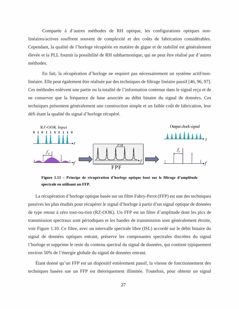
27
Comparée à d’autres méthodes de RH optique, les configurations optiques non-
linéaires/actives souffrent souvent de complexité et des coûts de fabrication considérables.
Cependant, la qualité de l’horloge récupérée en matière de gigue et de stabilité est généralement
élevée et la PLL fournit la possibilité de RH subharmonique, qui ne peut être réalisé par d’autres
méthodes.
En fait, la récupération d’horloge ne requiert pas nécessairement un système actif/non-
linéaire. Elle peut également être réalisée par des techniques de filtrage linéaire passif [46, 96, 97].
Ces méthodes enlèvent une partie ou la totalité de l’information contenue dans le signal reçu et de
ne conserver que la fréquence de base associée au débit binaire du signal de données. Ces
techniques présentent généralement une construction simple et un faible coût de fabrication, leur
défi étant la qualité du signal d’horloge récupéré.
Figure 1.11 – Principe de récupération d’horloge optique basé sur le filtrage d’amplitude
spectrale en utilisant un FFP.
La récupération d’horloge optique basée sur un filtre Fabry-Perot (FFP) est une des techniques
passives les plus étudiés pour récupérer le signal d’horloge à partir d’un signal optique de données
de type retour à zéro tout-ou-rien (RZ-OOK). Un FFP est un filtre d’amplitude dont les pics de
transmission spectraux sont périodiques et les bandes de transmission sont généralement étroite,
voir Figure 1.10. Ce filtre, avec un intervalle spectrale libre (ISL) accordé sur le débit binaire du
signal de données optiques entrant, préserve les composantes spectrales discrètes du signal
l’horloge et supprime le reste du contenu spectral du signal de données, qui contient typiquement
environ 50% de l’énergie globale du signal de données entrant.
Étant donné qu’un FFP est un dispositif entièrement passif, la vitesse de fonctionnement des
techniques basées sue un FFP est théoriquement illimitée. Toutefois, pour obtenir un signal
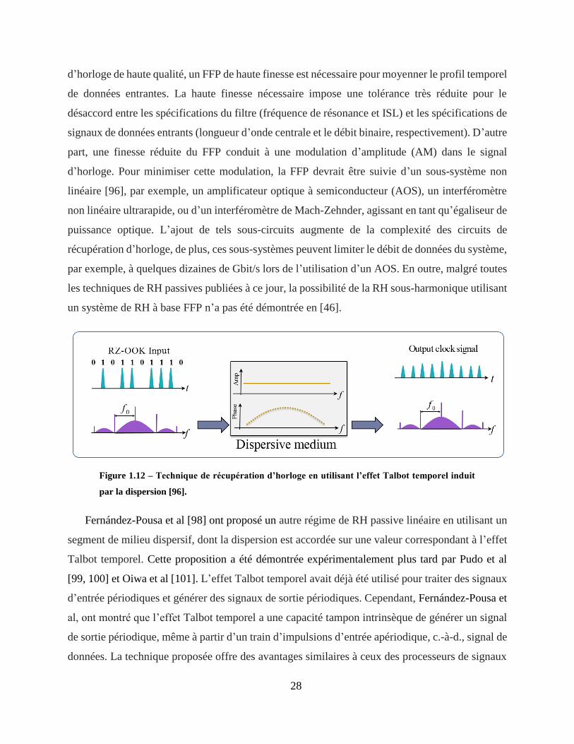
28
d’horloge de haute qualité, un FFP de haute finesse est nécessaire pour moyenner le profil temporel
de données entrantes. La haute finesse nécessaire impose une tolérance très réduite pour le
désaccord entre les spécifications du filtre (fréquence de résonance et ISL) et les spécifications de
signaux de données entrants (longueur d’onde centrale et le débit binaire, respectivement). D’autre
part, une finesse réduite du FFP conduit à une modulation d’amplitude (AM) dans le signal
d’horloge. Pour minimiser cette modulation, la FFP devrait être suivie d’un sous-système non
linéaire [96], par exemple, un amplificateur optique à semiconducteur (AOS), un interféromètre
non linéaire ultrarapide, ou d’un interféromètre de Mach-Zehnder, agissant en tant qu’égaliseur de
puissance optique. L’ajout de tels sous-circuits augmente de la complexité des circuits de
récupération d’horloge, de plus, ces sous-systèmes peuvent limiter le débit de données du système,
par exemple, à quelques dizaines de Gbit/s lors de l’utilisation d’un AOS. En outre, malgré toutes
les techniques de RH passives publiées à ce jour, la possibilité de la RH sous-harmonique utilisant
un système de RH à base FFP n’a pas été démontrée en [46].
Figure 1.12 – Technique de récupération d’horloge en utilisant l’effet Talbot temporel induit
par la dispersion [96].
Fernández-Pousa et al [98] ont proposé un autre régime de RH passive linéaire en utilisant un
segment de milieu dispersif, dont la dispersion est accordée sur une valeur correspondant à l’effet
Talbot temporel. Cette proposition a été démontrée expérimentalement plus tard par Pudo et al
[99, 100] et Oiwa et al [101]. L’effet Talbot temporel avait déjà été utilisé pour traiter des signaux
d’entrée périodiques et générer des signaux de sortie périodiques. Cependant, Fernández-Pousa et
al, ont montré que l’effet Talbot temporel a une capacité tampon intrinsèque de générer un signal
de sortie périodique, même à partir d’un train d’impulsions d’entrée apériodique, c.-à-d., signal de
données. La technique proposée offre des avantages similaires à ceux des processeurs de signaux
29
à base de l’effet Talbot, à savoir la simplicité, le potentiel d’atténuation de la gigue temporelle et
un rendement énergétique élevé. Cette dernière est due au fait que, fondamentalement, aucune
énergie n’est perdue dans le processus de récupération, car cette technique n’implique que les
manipulations de l’information de phase spectral du signal. Cette technique sera décrite en détail
plus loin dans la section 3.3.
1.3.2 Conversion de formats RZ à NRZ optiques
Les réseaux optiques du futur seraient probablement des hybrides de différentes technologies
en raison de la grande variété d’applications et de leur structure hiérarchique, ce qui implique
diverses spécifications pour les différents segments de réseau. Dans ce contexte, un segment de
réseau utilise le format de modulation adéquat qui répond à ses exigences [102, 103]. Par
conséquent, les convertisseurs de format tout-optique sont d’une grande importance pour
interconnecter de façon transparente les différentes parties des réseaux, ce qui évite le recours aux
convertisseurs optique-électrique (O/E) et électrique-optique (E/O), et éviter ainsi les limitations
imposées par l’électronique en matière de débit et de bande passante de fréquence [103]. En
particulier, la conversion entre les formats de signaux retour-à-zéro (RZ)7 et non-retour-à zéro
(NRZ)8 est particulièrement intéressante: les deux formats sont matures et largement utilisés dans
les différentes parties des réseaux, par exemple, le format RZ est adopté dans les systèmes de
multiplexage dans le domaine temporel (OTDM) pour être en mesure d’effectuer le multiplexage
d’impulsions, tandis que le format NRZ est préféré dans les systèmes de multiplexage en longueur
d’onde (WDM) en raison de sa plus grande efficacité spectrale [71]. En outre, la conversion de
format d’un signal RZ à son équivalent NRZ est également souhaitable dans de multiplexage des
signaux OTDM car les signaux NRZ améliorent la tolérance des processus de multiplexage à la
gigue temporelle grâce à leur forme temporelle à sommet plat [104].
7 Le retour à zéro (RZ) est un code de ligne utilisé dans les signaux de télécommunications dans lequel chaque
impulsion représentant 1 bit est choisie pour être plus courte que la durée de bits, et son amplitude retourne à zéro
avant que la durée de bit ne soit terminée. 8 Le non-retour à zéro (NRZ) est un code de ligne utilisé dans les signaux de télécommunications dans lequel chaque
impulsion représentant 1 bit occupe entièrement la durée de bit et ne tombe pas à zéro entre deux ou plusieurs bits
successifs.
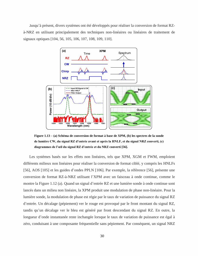
30
Jusqu’à présent, divers systèmes ont été développés pour réaliser la conversion de format RZ-
à-NRZ en utilisant principalement des techniques non-linéaires ou linéaires de traitement de
signaux optiques [104, 56, 105, 106, 107, 108, 109, 110].
Figure 1.13 – (a) Schéma de conversion de format à base de XPM, (b) les spectres de la sonde
de lumière CW, du signal RZ d’entrée avant et après la HNLF, et du signal NRZ converti, (c)
diagrammes de l’œil du signal RZ d’entrée et du NRZ converti [56].
Les systèmes basés sur les effets non linéaires, tels que XPM, XGM et FWM, emploient
différents milieux non linéaires pour réaliser la conversion de format ciblé, y compris les HNLFs
[56], AOS [105] et les guides d’ondes PPLN [106]. Par exemple, la référence [56], présente une
conversion de format RZ-à-NRZ utilisant l’XPM avec un faisceau à onde continue, comme le
montre la Figure 1.12 (a). Quand un signal d’entrée RZ et une lumière sonde à onde continue sont
lancés dans un milieu non linéaire, la XPM produit une modulation de phase non-linéaire. Pour la
lumière sonde, la modulation de phase est régie par le taux de variation de puissance du signal RZ
d’entrée. Un décalage (pépiement) ver le rouge est provoqué par le front montant du signal RZ,
tandis qu’un décalage ver le bleu est généré par front descendant du signal RZ. En outre, la
longueur d’onde instantanée reste inchangée lorsque le taux de variation de puissance est égal à
zéro, conduisant à une composante fréquentielle sans pépiement. Par conséquent, un signal NRZ
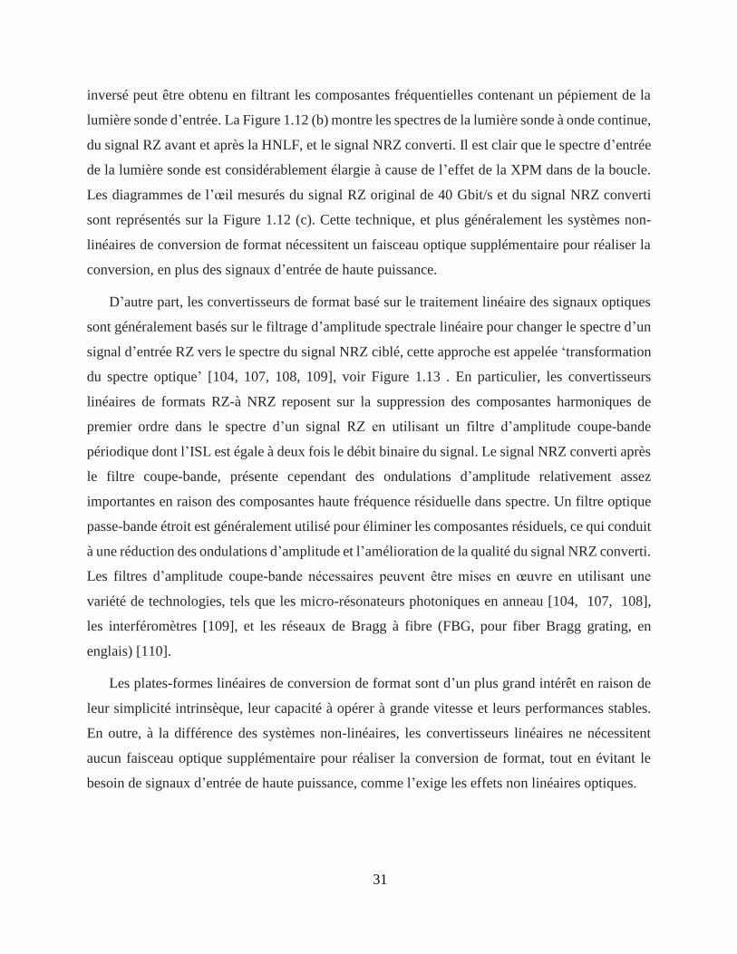
31
inversé peut être obtenu en filtrant les composantes fréquentielles contenant un pépiement de la
lumière sonde d’entrée. La Figure 1.12 (b) montre les spectres de la lumière sonde à onde continue,
du signal RZ avant et après la HNLF, et le signal NRZ converti. Il est clair que le spectre d’entrée
de la lumière sonde est considérablement élargie à cause de l’effet de la XPM dans de la boucle.
Les diagrammes de l’œil mesurés du signal RZ original de 40 Gbit/s et du signal NRZ converti
sont représentés sur la Figure 1.12 (c). Cette technique, et plus généralement les systèmes non-
linéaires de conversion de format nécessitent un faisceau optique supplémentaire pour réaliser la
conversion, en plus des signaux d’entrée de haute puissance.
D’autre part, les convertisseurs de format basé sur le traitement linéaire des signaux optiques
sont généralement basés sur le filtrage d’amplitude spectrale linéaire pour changer le spectre d’un
signal d’entrée RZ vers le spectre du signal NRZ ciblé, cette approche est appelée ‘transformation
du spectre optique’ [104, 107, 108, 109], voir Figure 1.13 . En particulier, les convertisseurs
linéaires de formats RZ-à NRZ reposent sur la suppression des composantes harmoniques de
premier ordre dans le spectre d’un signal RZ en utilisant un filtre d’amplitude coupe-bande
périodique dont l’ISL est égale à deux fois le débit binaire du signal. Le signal NRZ converti après
le filtre coupe-bande, présente cependant des ondulations d’amplitude relativement assez
importantes en raison des composantes haute fréquence résiduelle dans spectre. Un filtre optique
passe-bande étroit est généralement utilisé pour éliminer les composantes résiduels, ce qui conduit
à une réduction des ondulations d’amplitude et l’amélioration de la qualité du signal NRZ converti.
Les filtres d’amplitude coupe-bande nécessaires peuvent être mises en œuvre en utilisant une
variété de technologies, tels que les micro-résonateurs photoniques en anneau [104, 107, 108],
les interféromètres [109], et les réseaux de Bragg à fibre (FBG, pour fiber Bragg grating, en
englais) [110].
Les plates-formes linéaires de conversion de format sont d’un plus grand intérêt en raison de
leur simplicité intrinsèque, leur capacité à opérer à grande vitesse et leurs performances stables.
En outre, à la différence des systèmes non-linéaires, les convertisseurs linéaires ne nécessitent
aucun faisceau optique supplémentaire pour réaliser la conversion de format, tout en évitant le
besoin de signaux d’entrée de haute puissance, comme l’exige les effets non linéaires optiques.
32
Figure 1.14 – Évolution des spectres (rangée du haut) et des formes d’onde temporelles (rangée
du bas) pour la conversion de format de RZ à NRZ basé sur la transformation de spectre
optique. f : fréquence, t : temps.
1.3.3 Méthodes de génération des impulsions optiques picoseconde pour les
systèmes optiques à haute vitesse
Les trains d’impulsions optiques picoseconde dans le régime gigahertz (GHz) et au-delà sont
d’un intérêt fondamental pour une très large gamme d’applications dans les domaines de
communications par fibre optique [111], l’informatique optique [112], la photonique micro-ondes
[113], le traitement des matériaux [114], les peignes de fréquences [115], l’optique non linéaire
[116] etc. En particulier, dans le cadre des communications optiques, les systèmes OTDM
nécessitent des sources optiques impulsionnels stables à taux de répétition élevé qui peuvent agir
à la fois, comme une source de données de transmission, et comme une horloge optique utilisée
pour synchroniser le signal et en extraire l’information transmise. La synchronisation temporelle
est également d’une grande importance dans les processeurs de signaux optiques, y compris les
régénérateurs et les circuits logiques [112, 44]. Afin d’assurer la synchronisation dans un circuit
optique de traitement du signal, une horloge optique de référence unique, à savoir, un train
d’impulsion à taux de répétition élevé, peut être utilisée. Les circuits optiques sont souvent
33
constitués d’un certain nombre d’opérations rapides, synchronisées les unes aux autres, mais
fonctionnant à des vitesses différentes selon la fonction qu’ils remplissent. Les unités de traitement
optiques centrales fonctionnent souvent à un taux de référence, tandis que les unités de traitement
optique dans les circuits périphériques peuvent fonctionner à des taux sensiblement supérieurs ou
inférieurs. Par conséquent, une source d’impulsion optique fiable à haut taux de répétition avec la
possibilité de programmer le taux de répétition de quelques GHz à plusieurs centaines de GHz est
nécessaire.
Un autre champ d’application potentiel des sources d’impulsions à haute vitesse réside à
l’interface entre l’optique et des dispositifs dont le spectre opérationnel se situe dans et au-dessus
de la plage des micro-ondes [113]. Pour commencer, certains systèmes électroniques peuvent
exiger des taux d’échantillonnage hyperfréquences dans les convertisseurs analogique-
numérique [117]. Dans ce cas, les impulsions optiques peuvent être utilisées pour générer une
courte rafale d’électrons, qui agissent ensuite comme un train d’impulsions d’échantillonnage dans
la gamme sous-THz. L’interface des technologies d’ondes optiques et millimétrique est
suffisamment importante pour être considérée comme un domaine séparé, à savoir la photonique
micro-onde, pour lequel les trains d’impulsions optiques à taux de répétition élevé sont
particulièrement importants.
Parmi un grand nombre de caractéristiques souhaitables d’une source d’impulsions optique à
haut taux de répétition utilisée dans les applications mentionnées ci-dessus, on peut inclure la
stabilité d’impulsions, la faible gigue temporelle, et les faibles fluctuations d’amplitude, en
particulier pour les applications utilisant le train d’impulsions comme référence ou comme signal
horloge d’échantillonnage.
Un grand nombre de sources laser d’impulsions courtes à taux de répétition élevé a été
démontré à ce jour. Les lasers à fibre ultrarapides offrent une plate-forme immédiate et attractive
pour la génération de trains d’impulsions à haut taux de répétition [118]. Dans les premières
démonstrations visant à réaliser de sources d’impulsions à taux de répétition élevés, les systèmes
laser à verrouillage actif de modes ont été utilisés, avec des taux de répétition démontrés allant
jusqu’à ~ 40 GHz. Toutefois, la bande passante des modulateurs et de leurs circuits électroniques
de contrôle empêche d’augmenter plus le taux de répétition de ces sources.
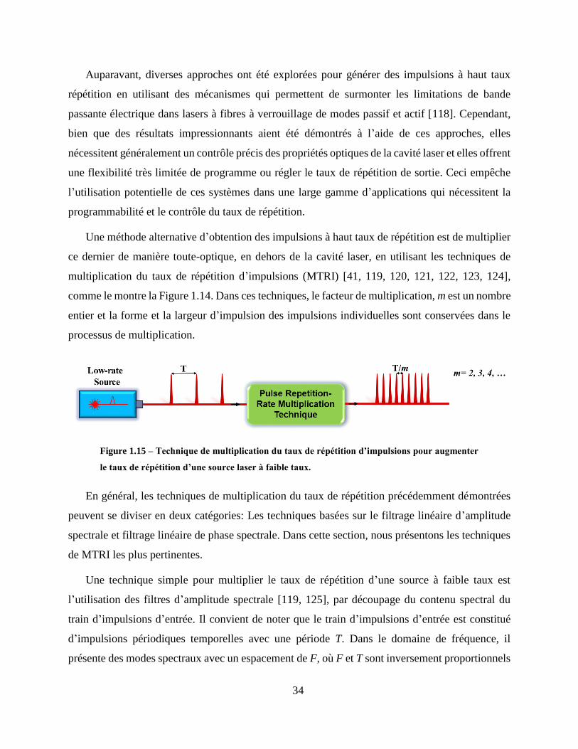
34
Auparavant, diverses approches ont été explorées pour générer des impulsions à haut taux
répétition en utilisant des mécanismes qui permettent de surmonter les limitations de bande
passante électrique dans lasers à fibres à verrouillage de modes passif et actif [118]. Cependant,
bien que des résultats impressionnants aient été démontrés à l’aide de ces approches, elles
nécessitent généralement un contrôle précis des propriétés optiques de la cavité laser et elles offrent
une flexibilité très limitée de programme ou régler le taux de répétition de sortie. Ceci empêche
l’utilisation potentielle de ces systèmes dans une large gamme d’applications qui nécessitent la
programmabilité et le contrôle du taux de répétition.
Une méthode alternative d’obtention des impulsions à haut taux de répétition est de multiplier
ce dernier de manière toute-optique, en dehors de la cavité laser, en utilisant les techniques de
multiplication du taux de répétition d’impulsions (MTRI) [41, 119, 120, 121, 122, 123, 124],
comme le montre la Figure 1.14. Dans ces techniques, le facteur de multiplication, m est un nombre
entier et la forme et la largeur d’impulsion des impulsions individuelles sont conservées dans le
processus de multiplication.
Figure 1.15 – Technique de multiplication du taux de répétition d’impulsions pour augmenter
le taux de répétition d’une source laser à faible taux.
En général, les techniques de multiplication du taux de répétition précédemment démontrées
peuvent se diviser en deux catégories: Les techniques basées sur le filtrage linéaire d’amplitude
spectrale et filtrage linéaire de phase spectrale. Dans cette section, nous présentons les techniques
de MTRI les plus pertinentes.
Une technique simple pour multiplier le taux de répétition d’une source à faible taux est
l’utilisation des filtres d’amplitude spectrale [119, 125], par découpage du contenu spectral du
train d’impulsions d’entrée. Il convient de noter que le train d’impulsions d’entrée est constitué
d’impulsions périodiques temporelles avec une période T. Dans le domaine de fréquence, il
présente des modes spectraux avec un espacement de F, où F et T sont inversement proportionnels
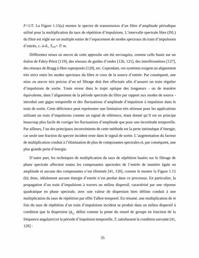
35
F=1/T. La Figure 1.15(a) montre le spectre de transmission d’un filtre d’amplitude périodique
utilisé pour la multiplication du taux de répétition d’impulsions. L’intervalle spectrale libre (ISL)
du filtre est réglé sur un multiple entier de l’espacement de modes spectraux du train d’impulsions
d’entrée, c.-à-d., Tout= T/ m.
Différentes mises en œuvre de cette approche ont été envisagées, comme celle basée sur un
étalon de Fabry-Pérot [119], des réseaux de guides d’ondes [126, 121], des interféromètres [127],
des réseaux de Bragg à fibre superposés [120], etc. Cependant, ces systèmes exigent un alignement
très strict entre les modes spectraux du filtre et ceux de la source d’entrée. Par conséquent, une
mise en œuvre très précise d’un tel filtrage doit être effectuée afin d’assurer un train régulier
d’impulsions de sortie. Toute erreur dans le trajet optique des longueurs - ou de manière
équivalente, dans l’alignement de la période spectrale du filtre par rapport aux modes de source -
introduit une gigue temporelle et des fluctuations d’amplitude d’impulsion à impulsion dans le
train de sortie. Cette déficience peut représenter une limitation très sérieuse pour les applications
utilisant un train d’impulsions comme un signal de référence, étant donné qu’il est en principe
beaucoup plus facile de corriger les fluctuations d’amplitude que pour une incertitude temporelle.
Par ailleurs, l’un des principaux inconvénients de cette méthode est la perte intrinsèque d’énergie,
car seule une fraction du spectre incident reste dans le signal de sortie. L’augmentation du facteur
de multiplication conduit à l’élimination de plus de composantes spectrales et, par conséquent, une
plus grande perte d’énergie.
D’autre part, les techniques de multiplication du taux de répétition basées sur le filtrage de
phase spectrale affectent toutes les composantes spectrales de l’entrée de manière égale en
amplitude et aucune des composantes n’est éliminée [41, 120], comme le montre la Figure 1.15
(b); donc, idéalement aucune énergie d’entrée n’est perdue dans ce processus. En particulier, la
propagation d’un train d’impulsions à travers un milieu dispersif, caractérisé par une réponse
quadratique en phase spectrale, avec une valeur de dispersion bien définie conduit à une
multiplication du taux de répétition par effet Talbot temporel. En résumé, une multiplication de m
fois du taux de répétition d’un train d’impulsions incident se produit dans un milieu dispersif à
condition que la dispersion (ϕ2
, défini comme la pente du retard de groupe en fonction de la
fréquence angulaire) et la période d’impulsion temporelle, T, satisfassent la condition suivante [41,
120] :
36
ϕ2
= =s
m
T 2
2π (1.4)
où m et s sont des nombres entiers tels que s/m est un nombre rationnel irréductible. Une
explication plus détaillée de cette technique sera fournie dans le Chapitre 2.
Figure 1.16 – Techniques de multiplication du taux de répétition d’impulsions basé sur le
filtrage linéaire (a) d’amplitude spectrale et (b) de phase spectrale.
La multiplication du taux de répétition d’impulsions basée sur l’effet Talbot temporel a attiré
beaucoup d’attention au cours des années grâce à sa mise en œuvre simple, avec une complexité
sensiblement réduite en comparaison avec les méthodes de filtrage d’amplitude spectrale. Cette
approche fournit la copie d’un train d’impulsions optiques entrant avec le taux de répétition
multiplié tel que désiré, simplement par un procédé de filtrage de phase spectrale-seule induit par
une dispersion appropriée. En outre, cette méthode (i) offre une meilleure efficacité énergétique,
car fondamentalement l’énergie est conservée dans le filtrage de phase-seule, (ii) offre des

37
capacités d’atténuation du bruit de phase et d’amplitude, et (iii) elle est robuste contre les
désalignements possibles entre le filtre et la source d’entrée.
Cependant, malgré son ensemble attrayant d’avantages, la technique de MTRI à base d’effet
Talbot nécessite l’utilisation d’une quantité dispersion adéquate fixée, pour réaliser un facteur de
multiplication donné; une fois que la dispersion est fixé, généralement en utilisant une section
d’une fibre dispersive ou un réseau de Bragg à fibre (FBG, pour fiber Bragg grating) à pas variable,
il est difficile de régler ou de programmer le facteur de multiplication du taux sans changement
importants de la configuration du système ( par exemple, en changeant le milieu dispersif). En
outre, le procédé est limité à des taux de répétition de sortie qui ne sont que des multiples entiers
du taux de répétition initial, c.-à-d., m est un nombre entier. Cette même restriction fondamentale
s’applique à toutes les méthodes de MTRI publiées à ce jour.
38
1.4 Objectif et Organisation de la Thèse
La consommation d’énergie, et les problèmes thermiques associés, ont été une préoccupation
principale et qui a motivé la plupart des progrès réalisés par l’industrie électronique au cours du
dernier demi-siècle. En comparaison, la communauté de recherche de traitement du signal optique
a prêté peu d’attention à la question de la consommation d’énergie. Il est souvent avancé que le
traitement du signal optique remplacera le traitement du signal numérique en raison de ses
capacités de haute vitesse. Toutefois, les arguments simplistes basés sur la vitesse seule manquent
souvent le point d’importance critique que les dispositifs optiques sont généralement très
gourmands en énergie. À moins qu’il n’y ait une amélioration de plusieurs ordres de grandeur dans
l’efficacité énergétique des processeurs optiques, l’électronique est susceptible de rester la
technologie de choix pour la grande majorité d’applications de traitement du signal et de
commutation dans les réseaux de télécommunication.
Un des objectifs clés de cette thèse est de mettre en évidence l’importance de la consommation
d’énergie en tant que mesure de la performance dans le traitement du signal optique et d’essayer
de fournir une solution technologique au problème de la consommation d’énergie dans les
processeurs optiques pertinents. En particulier, dans cette thèse, nous explorons la possibilité
d’utiliser des techniques linéaires passives/actives pour le traitement du signal optique économe
en énergie, en évitant l’utilisation de mécanismes optiques classiques actifs et/ou non-linéaires
gourmands en énergie; nous choisissons un système de modulation temporelle linéaire actif, à
savoir, la modulation électro-optique, qui fournit le mécanisme de modulation temporelle d’un
signal optique le plus simple et le plus efficace en énergie (c.-à-d., ayant la plus faible
consommation d’énergie). En particulier, nous introduisons de nouveaux concepts et des
approches novatrices pour la mise en œuvre des opérations importantes de traitement du signal
optique en utilisant une modulation de phase temporelle et/ou le filtrage de phase spectrale qui
conservent intrinsèquement toute l’énergie du signal d’entrée sans nécessiter de sources de lumière
supplémentaires. Grâce à ces concepts, l’énergie du signal entrant est redistribuée efficacement
pour construire le signal de sortie visé, sans perte d’énergie et sans utiliser une puissance optique
externe supplémentaire.
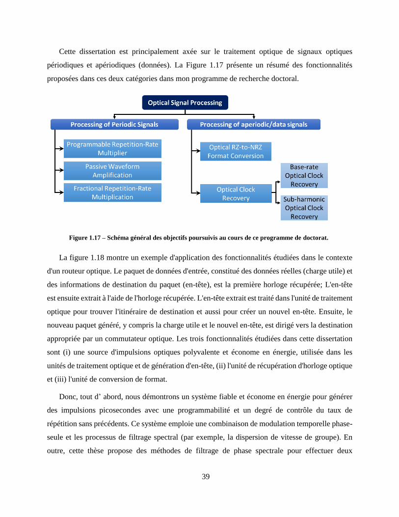
39
Cette dissertation est principalement axée sur le traitement optique de signaux optiques
périodiques et apériodiques (données). La Figure 1.17 présente un résumé des fonctionnalités
proposées dans ces deux catégories dans mon programme de recherche doctoral.
Figure 1.17 – Schéma général des objectifs poursuivis au cours de ce programme de doctorat.
La figure 1.18 montre un exemple d'application des fonctionnalités étudiées dans le contexte
d'un routeur optique. Le paquet de données d'entrée, constitué des données réelles (charge utile) et
des informations de destination du paquet (en-tête), est la première horloge récupérée; L'en-tête
est ensuite extrait à l'aide de l'horloge récupérée. L'en-tête extrait est traité dans l'unité de traitement
optique pour trouver l'itinéraire de destination et aussi pour créer un nouvel en-tête. Ensuite, le
nouveau paquet généré, y compris la charge utile et le nouvel en-tête, est dirigé vers la destination
appropriée par un commutateur optique. Les trois fonctionnalités étudiées dans cette dissertation
sont (i) une source d'impulsions optiques polyvalente et économe en énergie, utilisée dans les
unités de traitement optique et de génération d'en-tête, (ii) l'unité de récupération d'horloge optique
et (iii) l'unité de conversion de format.
Donc, tout d’ abord, nous démontrons un système fiable et économe en énergie pour générer
des impulsions picosecondes avec une programmabilité et un degré de contrôle du taux de
répétition sans précédents. Ce système emploie une combinaison de modulation temporelle phase-
seule et les processus de filtrage spectral (par exemple, la dispersion de vitesse de groupe). En
outre, cette thèse propose des méthodes de filtrage de phase spectrale pour effectuer deux
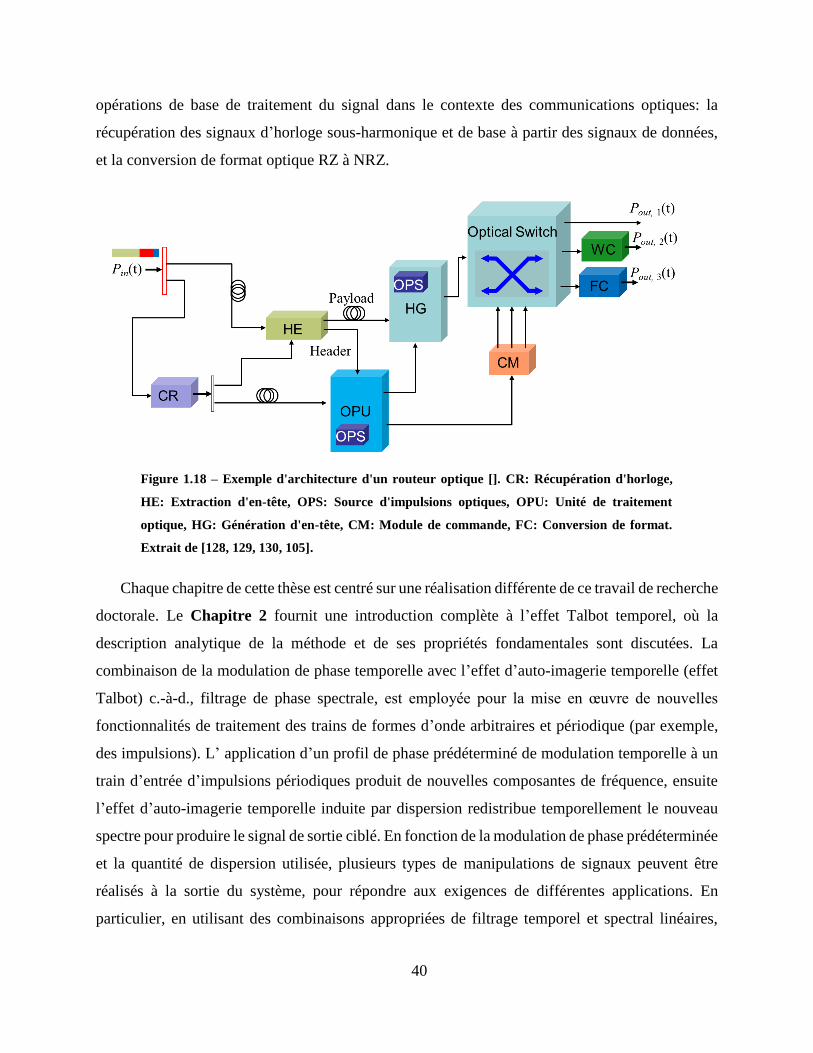
40
opérations de base de traitement du signal dans le contexte des communications optiques: la
récupération des signaux d’horloge sous-harmonique et de base à partir des signaux de données,
et la conversion de format optique RZ à NRZ.
Figure 1.18 – Exemple d'architecture d'un routeur optique []. CR: Récupération d'horloge,
HE: Extraction d'en-tête, OPS: Source d'impulsions optiques, OPU: Unité de traitement
optique, HG: Génération d'en-tête, CM: Module de commande, FC: Conversion de format.
Extrait de [128, 129, 130, 105].
Chaque chapitre de cette thèse est centré sur une réalisation différente de ce travail de recherche
doctorale. Le Chapitre 2 fournit une introduction complète à l’effet Talbot temporel, où la
description analytique de la méthode et de ses propriétés fondamentales sont discutées. La
combinaison de la modulation de phase temporelle avec l’effet d’auto-imagerie temporelle (effet
Talbot) c.-à-d., filtrage de phase spectrale, est employée pour la mise en œuvre de nouvelles
fonctionnalités de traitement des trains de formes d’onde arbitraires et périodique (par exemple,
des impulsions). L’ application d’un profil de phase prédéterminé de modulation temporelle à un
train d’entrée d’impulsions périodiques produit de nouvelles composantes de fréquence, ensuite
l’effet d’auto-imagerie temporelle induite par dispersion redistribue temporellement le nouveau
spectre pour produire le signal de sortie ciblé. En fonction de la modulation de phase prédéterminée
et la quantité de dispersion utilisée, plusieurs types de manipulations de signaux peuvent être
réalisés à la sortie du système, pour répondre aux exigences de différentes applications. En
particulier, en utilisant des combinaisons appropriées de filtrage temporel et spectral linéaires,
41
nous allons montrer (i) une technique programmable de multiplication de taux répétition, où le
taux de répétition de sortie peut être programmée électriquement pour être un multiple entier du
taux de répétition d’entrée; (ii) une technique fractionnaire de multiplication de taux de répétition,
où le taux de répétition du signal de sortie peut être ajusté pour être un multiple fractionnaire du
taux de répétition du signal d’entrée; (iii) des mécanismes de division de taux de répétition avec
conservation de l’énergie d’entrée, et produisant donc, une amplification passive de chaque forme
d’onde individuelle sans distorsions, c.-à-d., un amplificateur de forme d’onde passive sans
utilisation de gain actif.
Le Chapitre 3 introduit de nouveaux concepts et technologies de traitement de signaux
économes en énergie pour les signaux de données optiques. A cette fin, nous définissons,
concevons et développons deux ensembles pertinents de processeurs: (i) Une nouvelle approche
toute-optique de conversion de format de données de télécommunication retour-à-zéro (RZ) -à-
non-RZ (NRZ), qui a été expérimentalement mise en œuvre avec un débit de 640 Gbit/s. Dans
cette approche, nous montrons comment une manipulation adéquate de phase-seule des
composantes fréquentielles d’un signal de données RZ peut être utilisée pour réaliser la conversion
vers le signal NRZ équivalent. (ii) de nouvelles approches pour la récupération des signaux
d’horloge de base et sous-harmonique à partir de signaux de données tout ou rien (OOK). Le
premier de ces deux processeurs est réalisé en utilisant le filtrage optique linéaire de phase-seule
du signal RZ d’entrée, alors que le deuxième exploite l’effet appelé ‘auto-imagerie inverse ‘.
Le Chapitre 4 résume les travaux présentés dans cette thèse et propose des perspectives
potentielles pour les travaux futurs.

42
43
Chapter 1
1 Introduction
The transition of signal processing from electronics to optics in optical telecommunication
networks is described. Paramount practical concerns of present optical signal processors and
potential solutions are identified. Next, through an overview of optical signal processing
technologies, the foundation for this Thesis is established. The various contributions described in
the Thesis are presented and the structure of the Thesis is outlined.
1.1 Signal processing: Transition from electronics to optics?
Since the invention of “dielectric waveguides” in 1966 by Charles Kao and George Hockham
of Standard Telephone Cables (STC) Ltd. in Harlow of England [1], optical fiber communication
systems have used lightwaves as carriers to transmit information from one place to the other. The
distance of a few meters in laboratory was increased to a few kilometers, to hundreds of kilometers,
and now thousands of kilometers in the first decade of this century with bit rates reaching from
few tens of Mbit/s in late 1960s to 100 Gbit/s and tens of Tbit/s at present [2]. Tremendous progress
has been made through nearly the last 55 years due to significant advancements in (i) modulation
and detection techniques, so that the data bit rate of the early-stage communication systems, i.e.
100 Mb/s (1980), has been gradually increased to 40Gbit/s at a single wavelength, (ii) the
transmission technologies and hardware components, including multiplexing techniques such as
dense wavelength division multiplexing (DWDM)9, optical time-division multiplexing (OTDM)10,
optical orthogonal frequency-division multiplexing (OFDM)11, ultimately enabled by the
9 DWDM is an optical multiplexing technology for combining and transmitting multiple optical signals simultaneously
at different wavelengths on the same optical single-mode fiber. 10 OTDM is an optical multiplexing technology for combining and transmitting multiple optical signals at the same
wavelength on the same single-mode fiber. The signals are temporally multiplexed, and each signal appears on the
transmission line only a fraction of time in an alternating pattern. 11 Optical OFDM is a frequency division multiplexing technology. In contrast to WDM, optical OFDM subcarriers
overlap each other significantly and therefore has a higher spectral efficiency.
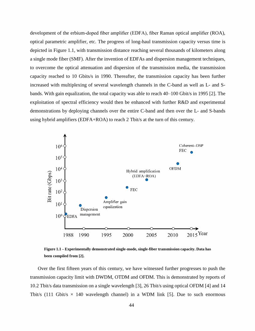
44
development of the erbium-doped fiber amplifier (EDFA), fiber Raman optical amplifier (ROA),
optical parametric amplifier, etc. The progress of long-haul transmission capacity versus time is
depicted in Figure 1.1, with transmission distance reaching several thousands of kilometers along
a single mode fiber (SMF). After the invention of EDFAs and dispersion management techniques,
to overcome the optical attenuation and dispersion of the transmission media, the transmission
capacity reached to 10 Gbits/s in 1990. Thereafter, the transmission capacity has been further
increased with multiplexing of several wavelength channels in the C-band as well as L- and S-
bands. With gain equalization, the total capacity was able to reach 40–100 Gbit/s in 1995 [2]. The
exploitation of spectral efficiency would then be enhanced with further R&D and experimental
demonstrations by deploying channels over the entire C-band and then over the L- and S-bands
using hybrid amplifiers (EDFA+ROA) to reach 2 Tbit/s at the turn of this century.
Figure 1.1 – Experimentally demonstrated single-mode, single-fiber transmission capacity. Data has
been compiled from [2].
Over the first fifteen years of this century, we have witnessed further progresses to push the
transmission capacity limit with DWDM, OTDM and OFDM. This is demonstrated by reports of
10.2 Tbit/s data transmission on a single wavelength [3], 26 Tbit/s using optical OFDM [4] and 14
Tbit/s (111 Gbit/s × 140 wavelength channel) in a WDM link [5]. Due to such enormous
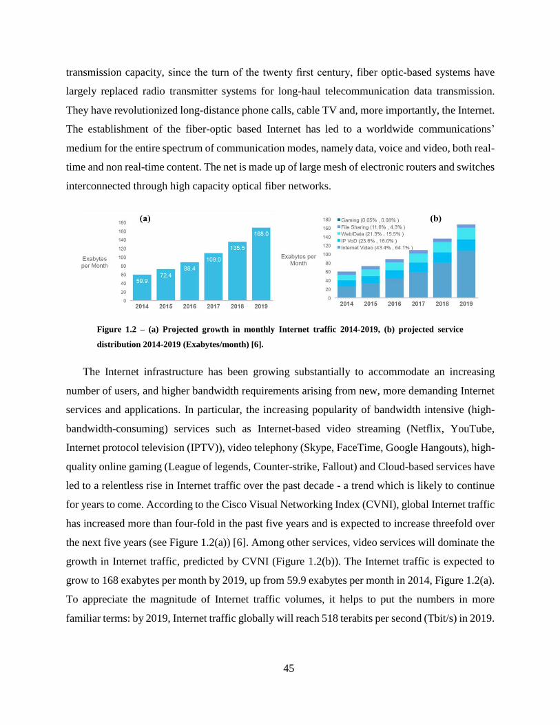
45
transmission capacity, since the turn of the twenty first century, fiber optic-based systems have
largely replaced radio transmitter systems for long-haul telecommunication data transmission.
They have revolutionized long-distance phone calls, cable TV and, more importantly, the Internet.
The establishment of the fiber-optic based Internet has led to a worldwide communications’
medium for the entire spectrum of communication modes, namely data, voice and video, both real-
time and non real-time content. The net is made up of large mesh of electronic routers and switches
interconnected through high capacity optical fiber networks.
Figure 1.2 – (a) Projected growth in monthly Internet traffic 2014-2019, (b) projected service
distribution 2014-2019 (Exabytes/month) [6].
The Internet infrastructure has been growing substantially to accommodate an increasing
number of users, and higher bandwidth requirements arising from new, more demanding Internet
services and applications. In particular, the increasing popularity of bandwidth intensive (high-
bandwidth-consuming) services such as Internet-based video streaming (Netflix, YouTube,
Internet protocol television (IPTV)), video telephony (Skype, FaceTime, Google Hangouts), high-
quality online gaming (League of legends, Counter-strike, Fallout) and Cloud-based services have
led to a relentless rise in Internet traffic over the past decade - a trend which is likely to continue
for years to come. According to the Cisco Visual Networking Index (CVNI), global Internet traffic
has increased more than four-fold in the past five years and is expected to increase threefold over
the next five years (see Figure 1.2(a)) [6]. Among other services, video services will dominate the
growth in Internet traffic, predicted by CVNI (Figure 1.2(b)). The Internet traffic is expected to
grow to 168 exabytes per month by 2019, up from 59.9 exabytes per month in 2014, Figure 1.2(a).
To appreciate the magnitude of Internet traffic volumes, it helps to put the numbers in more
familiar terms: by 2019, Internet traffic globally will reach 518 terabits per second (Tbit/s) in 2019.
46
This is the equivalent of 191 million people streaming Internet high-definition (HD) video
simultaneously, all day, every day, or equivalent to 42 billion DVDs per month.
The aforementioned capacity provided by optical transport technologies has continued to keep
ahead of the Internet traffic demand, and access to the required transmission capacity for the next
coming years is not far from realization. However, transmission capacity does not form the whole
picture in the communication networks. As mentioned above, the Internet and, in general, a
communication network basically has two functionalities: transmission and routing/switching [7].
Information in the form of bits is sent from an origin to a final destination through transmission
channels via many intermediate network nodes. At these nodes, the switching takes place so as to
route the bits from the origin to the destination along a prescribed pathway. The routing and
switching itself can be implemented in either the electrical or the optical domain. Switching in the
electrical domain is very efficient and the technology is mature. To date, the combination of optical
transmission and electrical routing works very well, as evidenced by the fact that so far in most of
the commercial networks, the information is transmitted in the optical domain and routed in the
electrical domain. However, the routing/switching in the electrical domain is experiencing greatly
increased pressure from the above-mentioned ever-increasing transmission capacity in optical
fibers.
Therefore, there is serious concern that the ultimate achievable capacity of the networks will
eventually be limited by so-called “bandwidth bottlenecks” in electronic routers, i.e. the bandwidth
imbalance between the optical transmissions and electronic routers [8, 9]. A router is composed
by many signal processing units and the overall capacity of the router depends on the speed of the
individual signal processing units [10]. Although the clock speed of the electronic signal
processing units for information processing increased linearly until a couple of years ago, it now
seems to be running out of steam, as shown in Figure 1.3. Also of concern is the large power
consumption and heat dissipation associated with the processing of data in electronic processors
in the routers, which is likely to become even more problematic as routers become even larger.
The situation becomes even worse when there are many wavelength channels in one optical fiber,
as is common in today’s DWDM networks, because a large number of optical receivers for optical
to electronic conversion (O/E conversion), modulators and lasers for electronic to optical
conversion (E/O conversion) will be required at each network nodes to interface electronic
47
processing circuits to the optical transmission medium, resulting in a prohibitively expensive
network. The Cisco CRS-1 router with up to 92 Tbit/s switch capacity (72 line card shelves, 400
Gbit/s line cards in one shelf) occupies 100m2 space, consumes 1 MW of power and weighs 60
Ton12.
Currently, electronic technologies are keeping up with the bandwidth demands using extensive
parallelism [11, 12], where the number of components and their combined power consumption,
simply scale with the bandwidth. Presently, in the developed countries, the total energy consumed
by the Internet’s infrastructure accounts for 2-3% of the overall worldwide energy consumption
[13] and the associated contribution to the global CO2 emissions [14, 15]. This share will only
keep increasing with serious consequences for the economy and the environment. This raises the
issue of whether Internet growth may ultimately be constrained by energy consumption rather than
by bandwidth! [16].
A number of solutions have been proposed to address bandwidth and power consumption
problems in electronic signal processing in routers, and in general, in any digital computing device.
In particular, three decades ago, researchers and developers suggested that a move to optical signal
processing technologies will greatly alleviate the bandwidth imbalance, in which optical signals
are processed and routed in the optical domain [17]. The claimed advantages include (i) higher
bandwidths due to the inherent broadband nature of optics beyond the capabilities of electronics,
and (ii) compatibility with the general idea of all-optical networking, in which data pass
transparently through the network from source to destination in optical form without undergoing
any O/E or E/O conversions, allowing lower power consumption, eventually reducing the cost
[18].
Optical signal processing primary nurtured big hopes as a platform faster than electronics to
carry out operations. However, today, some disillusion has replaced the early enthusiasm and in
the last ten years, this proposition has had increasing sceptics inside the optical community itself.
Indeed, the available speed of optical components massively outperforms the state of the art in
electronics, with potential processing speeds well above the THz regime. In Figure 1.3, the clock
rate of optical signal processing devices is compared with the rate of electronic processors.
12 http://www.cisco.com/en/US/products/ps5763/index.html
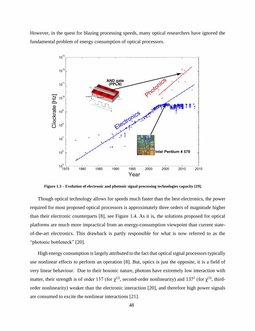
48
However, in the quest for blazing processing speeds, many optical researchers have ignored the
fundamental problem of energy consumption of optical processors.
Figure 1.3 – Evolution of electronic and photonic signal processing technologies capacity [19].
Though optical technology allows for speeds much faster than the best electronics, the power
required for most proposed optical processors is approximately three orders of magnitude higher
than their electronic counterparts [8], see Figure 1.4. As it is, the solutions proposed for optical
platforms are much more impractical from an energy-consumption viewpoint than current state-
of-the-art electronics. This drawback is partly responsible for what is now referred to as the
“photonic bottleneck” [20].
High energy consumption is largely attributed to the fact that optical signal processors typically
use nonlinear effects to perform an operation [8]. But, optics is just the opposite, it is a field of
very linear behaviour. Due to their bosonic nature, photons have extremely low interaction with
matter, their strength is of order 137 (for χ(2), second-order nonlinearity) and 1372 (for χ(3), third-
order nonlinearity) weaker than the electronic interaction [20], and therefore high power signals
are consumed to excite the nonlinear interactions [21].
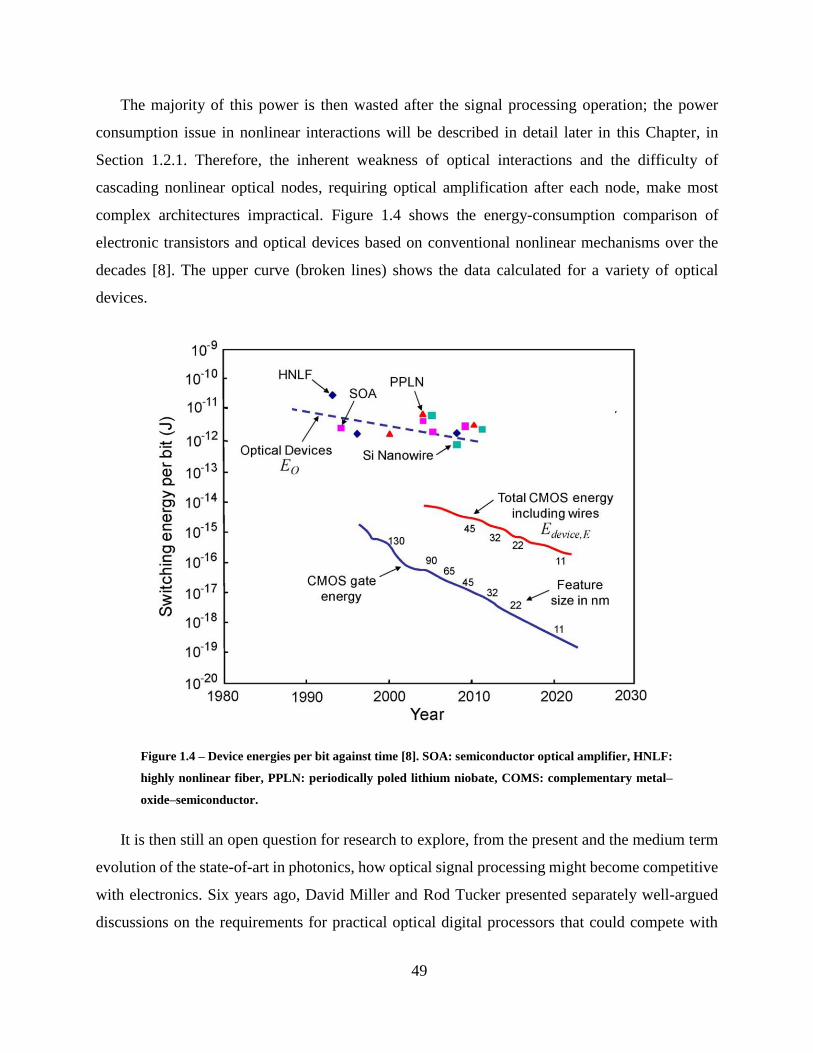
49
The majority of this power is then wasted after the signal processing operation; the power
consumption issue in nonlinear interactions will be described in detail later in this Chapter, in
Section 1.2.1. Therefore, the inherent weakness of optical interactions and the difficulty of
cascading nonlinear optical nodes, requiring optical amplification after each node, make most
complex architectures impractical. Figure 1.4 shows the energy-consumption comparison of
electronic transistors and optical devices based on conventional nonlinear mechanisms over the
decades [8]. The upper curve (broken lines) shows the data calculated for a variety of optical
devices.
Figure 1.4 – Device energies per bit against time [8]. SOA: semiconductor optical amplifier, HNLF:
highly nonlinear fiber, PPLN: periodically poled lithium niobate, COMS: complementary metal–
oxide–semiconductor.
It is then still an open question for research to explore, from the present and the medium term
evolution of the state-of-art in photonics, how optical signal processing might become competitive
with electronics. Six years ago, David Miller and Rod Tucker presented separately well-argued
discussions on the requirements for practical optical digital processors that could compete with
50
and surpass electronic devices [22, 23]. Unless, optical signal processors being at least as fast as
and more energy-efficient than their electronic counterparts, to the 10 fJ/bit level, are developed,
electronic technologies are likely to remain the technology of choice for the vast majority of signal
processors [23]. This may suggest that at least in the near future, optics will not become an
alternative to electronics in processing and computing.
However, despite this less hopeful outlook for optics in signal processing, some researchers
have remained optimistic. They argue that many advantages of optics in signal processing cannot
be overlooked and instead of abandoning it, new research should be conducted to resolve the
problems. Hence, for optical signal processing technologies to become a solid alternative to
electronics in information processing, switching and computing platforms, there is a strong need
for ground-breaking developments in optical science enabling novel breakthrough technologies
that will allow for increased capacity with a greatly reduced energy consumption. Indeed, optical
signal processing has been revisited during the last several years by addressing the remaining
limitations and (re)introducing (old)new optical signal processing techniques [24, 25, 26, 11, 27,
28, 29]. To this purpose, many approaches are being currently investigated for the possibility of
developing energy-efficienct optical signal processors. In particular, some research groups are
exploiting new optical waveguides with stronger nonlinearities to achieve a desired operation with
lower energy consumption [11, 30, 31, 32, 33]. Many researchers also believe that all-optical
processors may not be the most prudent goal [24, 34, 35, 36]. Instead, a hybrid approach, which
harvest the benefits from both electronics and optics to globally benefit from what is possible with
electronics and what is possible with optics, should be utilized. In addition, researchers are now
exploring the possibility of using purely passive and linear techniques for optical signal processing
[26, 25, 37, 38, 39, 40, 41], avoiding the use of conventional active and/or nonlinear mechanisms
in the signal-processing engines, potentially reducing the energy consumption significantly. In line
with these latest attempts, this Thesis deals with novel optical signal processing designs capable
of providing ultra-low-energy consumption. We have demonstrated energy efficient schemes,
comprising temporal and/or spectral phase manipulation of optical signals, for performing several
basic signal processing operations in the context of optical communications.
In this Chapter, we will first review the basis of optical signal processing technologies with an
emphasis on their energy-consumption performance. Finally, we conclude this introductory
51
Chapter with an outline of the state-of-the-art of a particular set of optical signal processing
functionalities of high relevance for this dissertation.
1.2 Optical signal processing and energy consumption
Optical signal processing is an enabling technology that encompasses the fundamental theory,
applications, algorithms, and implementations of processing or transferring information encoded
in a traveling light wave across the time and/or space domains — the optical signal. The main
focus of this Thesis is on time-domain optical signal processing, which is of great interest and use
in communication and computing systems.
Temporal optical signal processing has been under active investigation for many years,
bringing together various fields of optics and signal processing—namely, linear/nonlinear devices
and processes, the analog and digital signals—to achieve high-speed signal processing functions
that can potentially operate at the line rate of fiber optic communications. In particular, temporal
optical signal processing can generally be classified into two main categories: linear and nonlinear
signal processing, depending on whether they make use of optical nonlinear effects to perform
signal processing.
Within the context of optical signal processing, linear optical signal processing uses a rich
theoretical framework based on the early linear system theory and Fourier transforms, used
extensively in optics for the description of diffraction and spatial filtering. Linear signal processors
perform the target functionality on the input optical signal by deflecting, delaying and filtering the
signal but the frequency is unchanged and the fundamental principle of superposition holds.
Practice has shown that linear systems/processes emerge in a broad range of applications. In
contrast, nonlinear optics, known as the optics of intense light, is employed in optical processors
that require one or several optical beams to interact with each other without interference [42]. The
optical beams affect amplitude, phase, wavelength and polarization features of themselves or each
other’s as they propagate through the nonlinear medium and correspondingly, the superposition
principle is not valid.
There are many functionalities that are intrinsically nonlinear and we need a nonlinear
mechanisms to perform the related signal processing, such as wavelength conversion and
regeneration. However, there is a large number of functionalities that are either intrinsically linear,
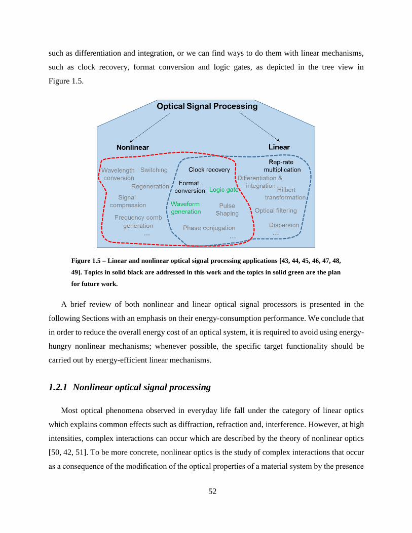
52
such as differentiation and integration, or we can find ways to do them with linear mechanisms,
such as clock recovery, format conversion and logic gates, as depicted in the tree view in
Figure 1.5.
Figure 1.5 – Linear and nonlinear optical signal processing applications [43, 44, 45, 46, 47, 48,
49]. Topics in solid black are addressed in this work and the topics in solid green are the plan
for future work.
A brief review of both nonlinear and linear optical signal processors is presented in the
following Sections with an emphasis on their energy-consumption performance. We conclude that
in order to reduce the overall energy cost of an optical system, it is required to avoid using energy-
hungry nonlinear mechanisms; whenever possible, the specific target functionality should be
carried out by energy-efficient linear mechanisms.
1.2.1 Nonlinear optical signal processing
Most optical phenomena observed in everyday life fall under the category of linear optics
which explains common effects such as diffraction, refraction and, interference. However, at high
intensities, complex interactions can occur which are described by the theory of nonlinear optics
[50, 42, 51]. To be more concrete, nonlinear optics is the study of complex interactions that occur
as a consequence of the modification of the optical properties of a material system by the presence

53
of an intense light. The light intensity levels that are required to observe optical nonlinear effects
are so high that they can usually not be observed in everyday life phenomena, and only can be
provided when using intense continuous-wave and pulsed lasers.
In a dielectric propagation medium, linear and nonlinear interactions with light can be
understood as an interaction between the light field and the atoms and molecules constituting the
medium. Materials are made up of atoms comprising charged particles (i.e. positive ions and
electrons) that are affected by the electric and magnetic fields. Dielectric materials have a neutral
charge distribution at a macroscopic scale and comprise an equal number of positive and negative
charges (positive ions and electrons) at the atomic scale. An incoming oscillating electric field E(t)
displaces the charges and exerts a separating action between the positive and negative charges
(dipole moment), changing the dipole moment per unit volume, or polarization P(t), of the material
(t is time variable). Notice that at visible/near-infrared frequencies, the electric field E(t) interacts
with dielectric materials mainly through negative charges (electrons). As long as the perturbation
of the initial trajectory of the charges is small, the displacement induced is linearly proportional to
the amplitude of the excitation field, E(t), described by
P(t) =ϵ0χ(1)E(t) (1.1)
where the constant of proportionality χ(1) is known as the linear susceptibility and ɛ0 is the
permittivity of free space. Stronger deformations of the charge distributions may lead to break this
proportional relationship and the optical response, polarization P(t), is then expressed by a power
series in the field strength E(t) as
P(t) =ϵ0[ χ(1)E(t) + χ(2)E2(t) + χ(3)E3(t) +…] (1.2)
The quantities χ(2) and χ(3) are known as the second- and third-order nonlinear optical
susceptibilities, respectively. For simplicity, we have taken the fields P(t) and E(t) to be scalar
quantities. We have also assumed that the polarization at time t depends only on the instantaneous
value of the electric field strength, implying (through the Kramers–Kronig relations) that the
medium must be lossless and dispersionless. We refer to P(2)(t) = ϵ0 χ(2)E2(t) as the second-order
nonlinear polarization and to P(3)(t) = ϵ0 χ(3)E3(t) as the third-order nonlinear polarization. Second-
order nonlinear optical interactions can occur only in noncentrosymmetric crystals such as Quartz

54
and lithium niobate (LiNbO3) —that is, in crystals that do not display inversion symmetry. Since
liquids, gases, amorphous solids (such as glass), and even many crystals display inversion
symmetry, χ(2) vanishes identically for such media, and consequently such materials cannot
produce second-order nonlinear optical interactions. On the other hand, third-order nonlinear
optical interactions (i.e., those described by a χ(3) susceptibility) can occur in centrosymmetric
media.
Nowadays, the application of nonlinear optics in the framework of information science has
two main motivations. Nonlinear effects are required for creating a substrate for processing optical
signals, whereas on the other hand, they cause detrimental distortions to long haul fibre optic
communication signals. Therefore, for signal processing applications, we require a propagation
medium with higher nonlinear effects to facilitate optical signal processing with lower cost in
energy. In sharp contrast, for optical signal transmission, one is interested in minimizing the effect
of nonlinearities of the propagation medium to increase transmission capacity. In the context of
optical signal processing, optical techniques employ a wide range of devices with various
nonlinear mechanisms to achieve multiple network functionalities. Several all-optical processing
technologies of significant interest are
- Semiconductor Optical Amplifiers (SOA) using χ(3) to excite cross-gain modulation
(XGM), self-phase modulation (SPM), cross phase modulation (XPM), and four-wave-
mixing (FWM) nonlinear effects [52, 53].
- Highly Nonlinear Fibers (HNLF) [54, 55, 56, 57] or other waveguides (Chalcogenide glass
[58], silicon-on-insulator (SOI) [59], and III-V semiconductor [60, 61]) using χ(3) to excite
SPM, XPM, FWM nonlinear effects.
- Periodically Poled Lithium Niobate (PPLN) using χ(2) to excite three wave mixing (TWM)
nonlinear effect [62, 63, 64].
All these platforms have been largely exploited, allowing to implement all-optical logic gates
[55], wavelength conversion [43], regeneration [44], frequency comb generation [45], etc. They
exhibit picosecond and sub-picosecond optical responses and therefore, potentially can construct
optical devices with a much faster dynamic than current electronic devices. But there is much more
to obtaining reliable high capacity optical systems than just high speed devices. The energy
consumption of the device is at least as important [8]. Because high intensity lights are required to
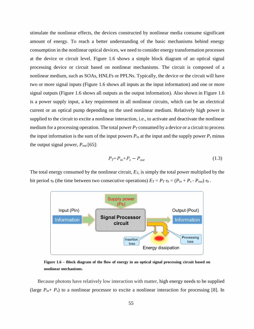
55
stimulate the nonlinear effects, the devices constructed by nonlinear media consume significant
amount of energy. To reach a better understanding of the basic mechanisms behind energy
consumption in the nonlinear optical devices, we need to consider energy transformation processes
at the device or circuit level. Figure 1.6 shows a simple block diagram of an optical signal
processing device or circuit based on nonlinear mechanisms. The circuit is composed of a
nonlinear medium, such as SOAs, HNLFs or PPLNs. Typically, the device or the circuit will have
two or more signal inputs (Figure 1.6 shows all inputs as the input information) and one or more
signal outputs (Figure 1.6 shows all outputs as the output information). Also shown in Figure 1.6
is a power supply input, a key requirement in all nonlinear circuits, which can be an electrical
current or an optical pump depending on the used nonlinear medium. Relatively high power is
supplied to the circuit to excite a nonlinear interaction, i.e., to activate and deactivate the nonlinear
medium for a processing operation. The total power PT consumed by a device or a circuit to process
the input information is the sum of the input powers Pin at the input and the supply power Ps minus
the output signal power, Pout [65]:
PT=Pin+Ps − Pout (1.3)
The total energy consumed by the nonlinear circuit, ET, is simply the total power multiplied by the
bit period τb (the time between two consecutive operations) ET = PT τb = (Pin + Ps - Pout) τb .
Figure 1.6 – Block diagram of the flow of energy in an optical signal processing circuit based on
nonlinear mechanisms.
Because photons have relatively low interaction with matter, high energy needs to be supplied
(large Pin+ Ps) to a nonlinear processor to excite a nonlinear interaction for processing [8]. In
56
addition to this large energy cost required to process the information, there are energy losses,
leading typically to heat generation. These are processing-energy loss and insertion loss [8].
Processing-energy loss comes from weak conversion of the input and supplied fields, Pin + Ps, into
the correct output information Pout. Because of light’s low interaction with matter, most of the
power in both the input and supplied fields, Pin +Ps, actually passes through the circuit unused, and
converted into heat, resulting in a small Pout (Pin +Ps >> Pout means large ET). Insertion loss comes
from the absorption and diffraction (spreading) of light when it propagates through the circuit, just
as any optical device cannot pass 100 percent of a lightwave. Additionally, optical signal
processing, in general, based on nonlinear interactions require continuous supply of energy,
regardless of whether that device is performing a processing operation or not [8].
In addition to energy concerns, the high degree of control required on the characteristics of the
input signals (e.g., power, central frequency, state of polarization, etc.) involved in a nonlinear
processing operation has hindered application of nonlinear optical signal processing beyond a
well-controlled laboratory environment. An additional drawback of nonlinear optical techniques
is that highly nonlinear fibers or waveguides with customized dispersion profiles are needed for an
efficient processing, making the system costly. Moreover, the implementation of more complex
systems relying on the concatenation of two or more nonlinear optical signal processors may
notably degrade the information signal’s quality. This degradation might be caused by the
reduction of the signal-to-noise ratio (associated to the low energy efficiency of these processors
and the requirement of amplification stages), and/or by the inclusion of spurious frequency
components in the bandwidth of the information signal.
1.2.2 Linear optical signal processing
Linear systems can be used to model and analyze a wide range of problems in science and
engineering. In particular, linear optical filters, which occupy a position of fundamental
importance in spatial and temporal optics have been studied extensively [41, 66, 67]. Linear optical
signal processing is founded in the rich theory of linear systems and in many applications, linear
processing methods prove to be optimal; two examples will be shown in Section 1.3. Moreover,
linear methods are inherently simple to implement, perhaps the dominant reason for their
widespread use in practice.
57
A processor is said to be linear if the transfer function, i.e. y = f(x), the function defining the
relationship between the input and output signals (x and y respectively), satisfies the principle of
superposition, such that f(x1+x2)=f(x1)+f(x2) and f(n x) = n f(x) [68]. That is, if an input to the system
consists of a weighted sum of several signals, the output of the system is the weighted sum (or
superposition) of the responses for each of the signals. The superposition property makes linear
systems easy to analyse, as it is possible to break down any linear signal into simple components
and analyse these separately.
If the parameters of the transfer function of the linear system are constant over the time of
interest, the signal processing operation is said to be time invariant [68]. A time shift in the input
signal causes the same time shift in the output signal. Sometimes such an operation is referred to
as a linear time invariant (LTI) processor. Quite often, such processors are assumed to be casual,
i.e. the present output signal depends on present and past signals, but not on future ones13.
Fourier analysis provides a set of powerful tools and insights for the design and understanding
of LTI systems. The impulse response and frequency response (spectral transfer function) are two
attributes that are useful for characterizing LTI systems. They provide two different complete ways
of calculating what an LTI system’s output will be for a given input signal. An LTI system’s
temporal impulse response, often annotated as h(t) with t being the time variable, is defined as the
output signal that results when an impulse is applied to the system input. By knowing the impulse
response, the output of the LTI system can be easily computed for any arbitrary input signal by
convolving the input signal with the impulse response function. Alternatively, the LTI system can
be characterized by a spectral transfer function H(ω) = V(ω)/U(ω) in the frequency domain where
U(ω) and V(ω) are the spectral Fourier transforms of the input and output signals of the system,
respectively, and ω is the angular frequency variable. There is a myriad of optical signal processing
functionalities that can be described by an LTI system response, see Figure 1.5, such as optical
13 A causal system (also known as a physical or nonanticipative system) is a system where the output depends on past
and current inputs but not future inputs, i.e., the output u(t0) only depends on the input v(t) for values of t ≤ t0 . In
general, the LTI systems operating on time-dependant signals are always casual and they cannot respond to the future
events. However, not all systems have time as an independent variable. If the independent variable is space, the system
does not need to be causal, i.e. the output u(x0) can depend on the input v(x) for all values of x, x ≤ x0 or x ≥ x0; for
example, a system that processes images.
58
clock recovery techniques, optical pulse shapers, optical differentiators/integrators, and pulse
processors such as Hilbert transformers, among many others.
In general, there exist two main procedures to implement linear optical signal processors, (i)
design of linear spectral filters, such as ring resonators, interferometers or fiber gratings, where the
filtering operation is realized by directly tailoring the input signal’s spectrum (Figure 1.7, left), (ii)
development of time-domain analogs of well-known spatial-domain filters in which the filtering
operation is carried out in the time domain via modulation processes (Figure 1.7, right). It is worth
mentioning that time-domain equivalents of spatial-domain optical filters have been identified and
created owing to the so-called space-time duality, which will be defined in detail in Chapter 2.
Using this duality, highly effective spatial-domain optical information processing techniques14 can
be applied on temporal domain signals, which ultimately enables more sophisticated and powerful
approaches to temporal processing and characterization of information [69]. Most notably, such
an approach has enabled development of the time-lens concept [69], temporal imaging/self-
imaging systems [41], real-time Fourier transformation and filtering [69], etc.
Linear temporal modulation and spectral filtering processes in turn can be divided in two
categories: amplitude and phase modulation/filtering. A desired signal manipulation can be
produced on the temporal (or spectral) amplitude or phase profile of the signal under test through
temporal (or spectral) intensity or phase modulation (filtering), as depicted in Figure 1.7.
An optical spectral amplitude filter with a transfer function of H(ω) = A(ω) exp[ jϕ(ω)], where
A(ω) and ϕ(ω) denote the amplitude and phase profiles of filter, respectively, modify the spectral
content of the input signal, and signal processing is typically carried out by attenuating and/or
removing some of the spectral components of the input signal, (Figure 1.7, left, top). Note that in
this type of filters, if ϕ(ω) = 0, the filter is called as an ideal amplitude-only filter, having an even
and non-casual impulse response. In practice, however, a spectral linear phase of ϕ(ω) = ω t0 is
typically introduced to satisfy the causality. This phase variation corresponds just to a temporal
delay of t0, so it does not affect the definition of the amplitude filter and it does not perform any
14 In spatial-domain processing, information is encoded in the spatial distribution of light, which propagates in free-
space. Processing of the spatial optical information is performed using free space optics [68], which involves the use
of optical lenses, diffraction gratings, spatial light modulators, etc.
59
other transformation on the input signal. Example of typical amplitude filters include ring
resonators [70, 49, 71], interferometers [72, 48] or periodic structures such as fiber or waveguide
gratings [73, 74]. On the other hand, an optical spectral phase-only (all-pass) filter is characterized
by a frequency response of H(ω) = A exp [ jϕ(ω)], where A is a constant amplitude, independent
of the frequency variable. Therefore, the spectral phase-only filter passes all spectral components
equally in amplitude; therefore, if the uniform spectral amplitude transfer function is designed for
100% transmission, fundamentally no signal energy is lost in the process (Figure 1.7, left, bottom).
Instead, the filter phase shifts the spectral components to carry out the target signal processing.
Typically, our intuition for the time-domain effects induced by a filter’s frequency response
amplitude on an incoming signal is rather well-developed, but in contrast, visualizing the effect of
the phase of the frequency response on the signal is subtler, but equally important. A dispersive
medium, such as a conventional single-mode optical fiber, is an example of a phase-only filter
[41].
Similarly, optical temporal intensity modulators with a modulation function of p(t) = A(t)
attenuates or eliminate some temporal components of the input signal to produce the target output
signal, see Figure 1.7, right, top. In contrast, as shown in Figure 1.7, right, bottom, a temporal
phase modulator with modulation function of p(t) = exp[ jϕ(t)] only modifies the phase of the light-
wave traversing it and, in essence, no signal energy is then lost in the process.
It should be noted that spectral filters are passive components, i.e., they do not require an
external source of energy to perform their intended functions. However, temporal modulators are
active components, which require an external energy source to operate and perform the target
functions. In this Thesis, whenever possible, we use energy-efficient passive linear spectral
filtering techniques to carry out a specific functionality. Nevertheless, not all functionalities can
be implemented using only passive systems and in many cases, we need to incorporate linear active
temporal modulation techniques. The simplest and most energy-efficient (i.e., the lowest
consuming energy) mechanism for temporal modulation of an optical signal can be achieved
through an electro-optic modulation scheme. In this scheme, the modulating signal is an electronic
signal, which intrinsically have lower energy than an optical signal. More importantly, electro-
optic modulation effect is induced using a second-order nonlinearity, which typically requires
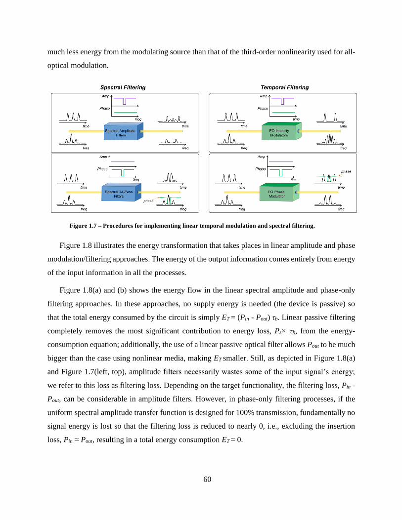
60
much less energy from the modulating source than that of the third-order nonlinearity used for all-
optical modulation.
Figure 1.7 – Procedures for implementing linear temporal modulation and spectral filtering.
Figure 1.8 illustrates the energy transformation that takes places in linear amplitude and phase
modulation/filtering approaches. The energy of the output information comes entirely from energy
of the input information in all the processes.
Figure 1.8(a) and (b) shows the energy flow in the linear spectral amplitude and phase-only
filtering approaches. In these approaches, no supply energy is needed (the device is passive) so
that the total energy consumed by the circuit is simply ET = (Pin - Pout) τb. Linear passive filtering
completely removes the most significant contribution to energy loss, Ps× τb, from the energy-
consumption equation; additionally, the use of a linear passive optical filter allows Pout to be much
bigger than the case using nonlinear media, making ET smaller. Still, as depicted in Figure 1.8(a)
and Figure 1.7(left, top), amplitude filters necessarily wastes some of the input signal’s energy;
we refer to this loss as filtering loss. Depending on the target functionality, the filtering loss, Pin -
Pout, can be considerable in amplitude filters. However, in phase-only filtering processes, if the
uniform spectral amplitude transfer function is designed for 100% transmission, fundamentally no
signal energy is lost so that the filtering loss is reduced to nearly 0, i.e., excluding the insertion
loss, Pin ≈ Pout, resulting in a total energy consumption ET ≈ 0.
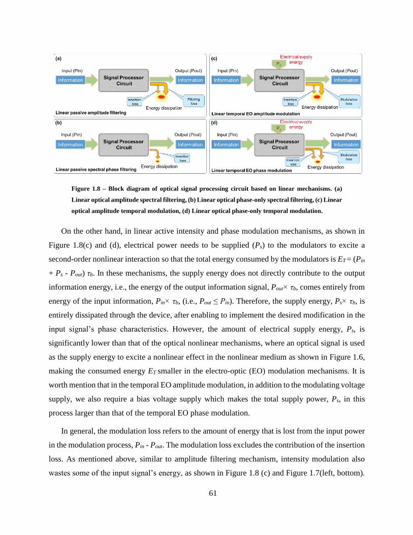
61
Figure 1.8 – Block diagram of optical signal processing circuit based on linear mechanisms. (a)
Linear optical amplitude spectral filtering, (b) Linear optical phase-only spectral filtering, (c) Linear
optical amplitude temporal modulation, (d) Linear optical phase-only temporal modulation.
On the other hand, in linear active intensity and phase modulation mechanisms, as shown in
Figure 1.8(c) and (d), electrical power needs to be supplied (Ps) to the modulators to excite a
second-order nonlinear interaction so that the total energy consumed by the modulators is ET = (Pin
+ Ps - Pout) τb. In these mechanisms, the supply energy does not directly contribute to the output
information energy, i.e., the energy of the output information signal, Pout× τb, comes entirely from
energy of the input information, Pin× τb, (i.e., Pout ≤ Pin). Therefore, the supply energy, Ps× τb, is
entirely dissipated through the device, after enabling to implement the desired modification in the
input signal’s phase characteristics. However, the amount of electrical supply energy, Ps, is
significantly lower than that of the optical nonlinear mechanisms, where an optical signal is used
as the supply energy to excite a nonlinear effect in the nonlinear medium as shown in Figure 1.6,
making the consumed energy ET smaller in the electro-optic (EO) modulation mechanisms. It is
worth mention that in the temporal EO amplitude modulation, in addition to the modulating voltage
supply, we also require a bias voltage supply which makes the total supply power, Ps, in this
process larger than that of the temporal EO phase modulation.
In general, the modulation loss refers to the amount of energy that is lost from the input power
in the modulation process, Pin - Pout. The modulation loss excludes the contribution of the insertion
loss. As mentioned above, similar to amplitude filtering mechanism, intensity modulation also
wastes some of the input signal’s energy, as shown in Figure 1.8 (c) and Figure 1.7(left, bottom).
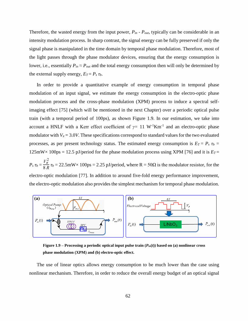
62
Therefore, the wasted energy from the input power, Pin - Pout, typically can be considerable in an
intensity modulation process. In sharp contrast, the signal energy can be fully preserved if only the
signal phase is manipulated in the time domain by temporal phase modulation. Therefore, most of
the light passes through the phase modulator devices, ensuring that the energy consumption is
lower, i.e., essentially Pin ≈ Pout and the total energy consumption then will only be determined by
the external supply energy, ET = Ps τb.
In order to provide a quantitative example of energy consumption in temporal phase
modulation of an input signal, we estimate the energy consumption in the electro-optic phase
modulation process and the cross-phase modulation (XPM) process to induce a spectral self-
imaging effect [75] (which will be mentioned in the next Chapter) over a periodic optical pulse
train (with a temporal period of 100ps), as shown Figure 1.9. In our estimation, we take into
account a HNLF with a Kerr effect coefficient of γ= 11 W-1Km-1 and an electro-optic phase
modulator with Vπ = 3.0V. These specifications correspond to standard values for the two evaluated
processes, as per present technology status. The estimated energy consumption is ET = Ps τb =
125mW× 100ps = 12.5 pJ/period for the phase modulation process using XPM [76] and it is ET =
Ps τb = Vπ
2
8 R τb = 22.5mW× 100ps = 2.25 pJ/period, where R = 50Ω is the modulator resistor, for the
electro-optic modulation [77]. In addition to around five-fold energy performance improvement,
the electro-optic modulation also provides the simplest mechanism for temporal phase modulation.
The use of linear optics allows energy consumption to be much lower than the case using
nonlinear mechanism. Therefore, in order to reduce the overall energy budget of an optical signal
Figure 1.9 – Processing a periodic optical input pulse train (Pin(t)) based on (a) nonlinear cross
phase modulation (XPM) and (b) electro-optic effect.
63
processing system, it is required to avoid the use of energy-hungry nonlinear mechanisms and to
implement the desired specific functionality using energy-efficient linear mechanisms.
1.3 Review of relevant optical signal processors studied in this
dissertation
Signal processing functions of importance studied in this dissertation are all-optical clock
recovery, optical format conversion and repetition-rate control of pulse lasers for telecom
applications. In this Section, we do a short and non-exhaustive review of some of the previously
demonstrated methods. The purpose of this discussion is to put our work into context.
1.3.1 Optical Clock Recovery
During the last 20 years a wide variety of optical “base-rate” and “sub-harmonic” clock
recovery (CR) methods based on different physical principles have been proposed and
demonstrated [78, 79, 46, 80, 81, 82, 83, 84, 85]. CR is a fundamental operation performed in all
digital communications devices ranging from ordinary mobile phones to high-speed optical
receivers. In optical telecommunications, the clock has traditionally been recovered with electrical
circuitry. For a conventional receiver converting the optical signal to an electrical one, the
electronic CR is the obvious choice. There are, however, locations and devices in the optical
network architecture, where the optical-to-electrical conversion is unnecessary. The preferred
choice would then be to preserve the signal in the optical domain. Such devices are, for example,
all-optical signal regenerators [44], time-division (de-) multiplexers [17], logical optical gates [55],
or, in general, locations where the transmitted signal needs to be (re-) timed but not terminated.
All digital telecommunications systems consist of three main building blocks: a transmitter, a
transmission path, and a receiver. The transmitter and the receiver are typically separated by a
considerable distance, therefore the receiver has no means to obtain direct information about the
transmitter clock. Naturally, the clock information could be sent through a separate communication
channel leading to reduced net bandwidth and increased costs of the system. Therefore, the receiver
typically recovers the clock from the incoming flow of bits.
64
Optical CR methods may be divided into two main categories: active/nonlinear and
passive/linear filtering techniques. In this Section, I provide a review of two optical CR methods,
one from each category.
A common active optical clock recovery technique is to use an optical phase-locked loop (PLL)
[86, 87]. The function of the optical PLL closely imitates a conventional electrical PLL that is
extensively used in applications of radio frequency (RF) and telecommunications technology. The
PLL synchronizes an internal oscillator with an external data signal. Through the synchronization
process the PLL obtains information about the frequency and the phase of the data signal, which
otherwise may be buried under the data modulation. Figure 1.10(a) shows the conventional
electrical PLL that is composed of four basic components: a phase detector (mixer), a low-pass
filter, a voltage-controlled oscillator (VCO), and a feedback loop [88, 89, 90]. Additionally, the
feedback loop may consist of a multiplication counter, when the resolved oscillation is a sub-
harmonic of the data signal.
The synchronization is made by adjusting the VCO such that the cross-correlation value of the
data and local signals is maximized. In a conventional electrical PLL, the input optical signal is
converted to the electronic signal in the input of the phase detector and mixed with the local signal
in order to realize the synchronization. However, in this configuration, the ultimate input bit rate
is limited by the phase detector response time [91, 46]. Alternative opto-electronic techniques have
been suggested to perform the required cross-correlation in the phase detector based on optical
nonlinear interactions to build an optical PLL. Figure 1.10(b) shows an example of an optical PLL
[92]. The required cross-correlation of the local optical clock and the data signals is performed
through four-wave mixing (FWM) in a nonlinear optical medium, such as an SOA [93], and three-
wave mixing (TWM) in periodically poled lithium niobate (PPLN) [78]. The pulses, depending on
the degree of overlap, interact through the FWM or TWM process and provide the cross-
correlation of the signals. The generated wavelength is bandpass filtered and the information about
the time averaged measured optical power is fed back to the VCO. Using this technique optical
clock recovery have been demonstrated at high data rates and de-multiplexing from a 320-Gbit/s
and a 640-Gbit/s OTDM stream [78, 94]. Recently, another nonlinear cross-correlation method
was introduced that is based on two-photon absorption in silicon avalanche photodiode [95]. The
time averaged photodiode response is dependent on the temporal overlap of the optical pulses and
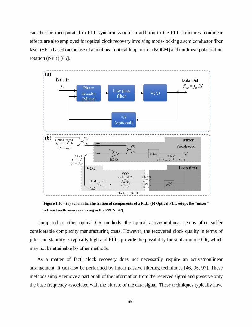
65
can thus be incorporated in PLL synchronization. In addition to the PLL structures, nonlinear
effects are also employed for optical clock recovery involving mode-locking a semiconductor fiber
laser (SFL) based on the use of a nonlinear optical loop mirror (NOLM) and nonlinear polarization
rotation (NPR) [85].
Figure 1.10 – (a) Schematic illustration of components of a PLL. (b) Optical PLL setup; the “mixer”
is based on three-wave mixing in the PPLN [92].
Compared to other optical CR methods, the optical active/nonlinear setups often suffer
considerable complexity manufacturing costs. However, the recovered clock quality in terms of
jitter and stability is typically high and PLLs provide the possibility for subharmonic CR, which
may not be attainable by other methods.
As a matter of fact, clock recovery does not necessarily require an active/nonlinear
arrangement. It can also be performed by linear passive filtering techniques [46, 96, 97]. These
methods simply remove a part or all of the information from the received signal and preserve only
the base frequency associated with the bit rate of the data signal. These techniques typically have
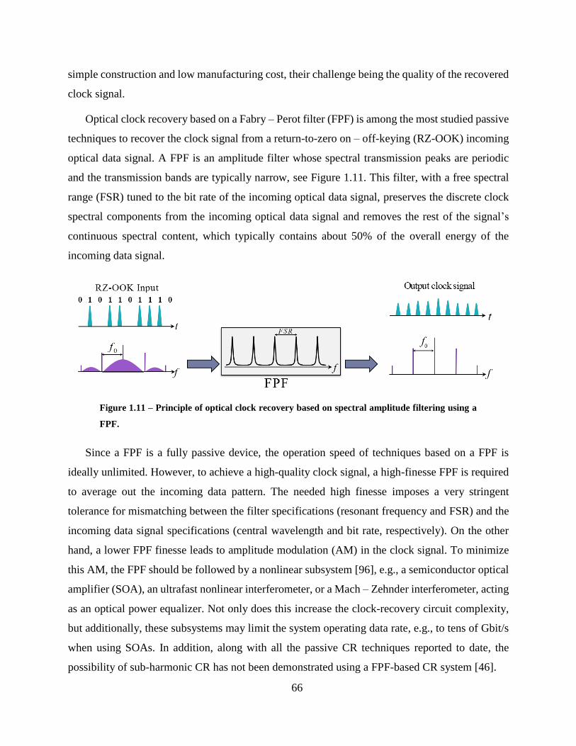
66
simple construction and low manufacturing cost, their challenge being the quality of the recovered
clock signal.
Optical clock recovery based on a Fabry – Perot filter (FPF) is among the most studied passive
techniques to recover the clock signal from a return-to-zero on – off-keying (RZ-OOK) incoming
optical data signal. A FPF is an amplitude filter whose spectral transmission peaks are periodic
and the transmission bands are typically narrow, see Figure 1.11. This filter, with a free spectral
range (FSR) tuned to the bit rate of the incoming optical data signal, preserves the discrete clock
spectral components from the incoming optical data signal and removes the rest of the signal’s
continuous spectral content, which typically contains about 50% of the overall energy of the
incoming data signal.
Figure 1.11 – Principle of optical clock recovery based on spectral amplitude filtering using a
FPF.
Since a FPF is a fully passive device, the operation speed of techniques based on a FPF is
ideally unlimited. However, to achieve a high-quality clock signal, a high-finesse FPF is required
to average out the incoming data pattern. The needed high finesse imposes a very stringent
tolerance for mismatching between the filter specifications (resonant frequency and FSR) and the
incoming data signal specifications (central wavelength and bit rate, respectively). On the other
hand, a lower FPF finesse leads to amplitude modulation (AM) in the clock signal. To minimize
this AM, the FPF should be followed by a nonlinear subsystem [96], e.g., a semiconductor optical
amplifier (SOA), an ultrafast nonlinear interferometer, or a Mach – Zehnder interferometer, acting
as an optical power equalizer. Not only does this increase the clock-recovery circuit complexity,
but additionally, these subsystems may limit the system operating data rate, e.g., to tens of Gbit/s
when using SOAs. In addition, along with all the passive CR techniques reported to date, the
possibility of sub-harmonic CR has not been demonstrated using a FPF-based CR system [46].

67
Fernández-Pousa et al [98] have proposed another linear passive CR scheme using a piece of
dispersive medium, whose dispersion is tuned to a value according to the temporal Talbot effect.
This proposal has been demonstrated experimentally later by Pudo et al [99, 100] and Oiwa et al
[101]. Temporal Talbot effect had already been used to process periodic input signals to generate
periodic output signals. However, Fernández-Pousa et al, showed that the temporal Talbot effect
has an inherent buffering ability to generate a periodic output, even from an aperiodic input pulse
train, i.e. data signal. The proposed technique offers similar advantages to those of the
conventional Talbot-based signal processors, namely simplicity, the potential for timing-jitter
mitigation and high energy efficiency. The latest is associated with the fact that fundamentally, no
energy is lost in the recovery process, since this involves only manipulations of the signal’s phase
information in the frequency domains. This technique will be described in deeper detail in
Section 3.3.
Figure 1.12 – Optical clock recovery technique through dispersion-induced temporal Talbot
effect [100].
1.3.2 Optical RZ to NRZ format conversion
Future optical networks are likely a hybrid scenario of various technologies owing to the large
variety of applications and to their hierarchical structure, which implies diverse specifications for
different networks’ segments. In this context, a specific network segment employs an adequate
modulation format that meets its requirements [102, 103]. Therefore, all-optical format converters
are of great importance to transparently and seamlessly interconnect different parts of the
networks, avoiding the use of optical-to-electrical (O/E) and electrical-to-optical (E/O) converters,
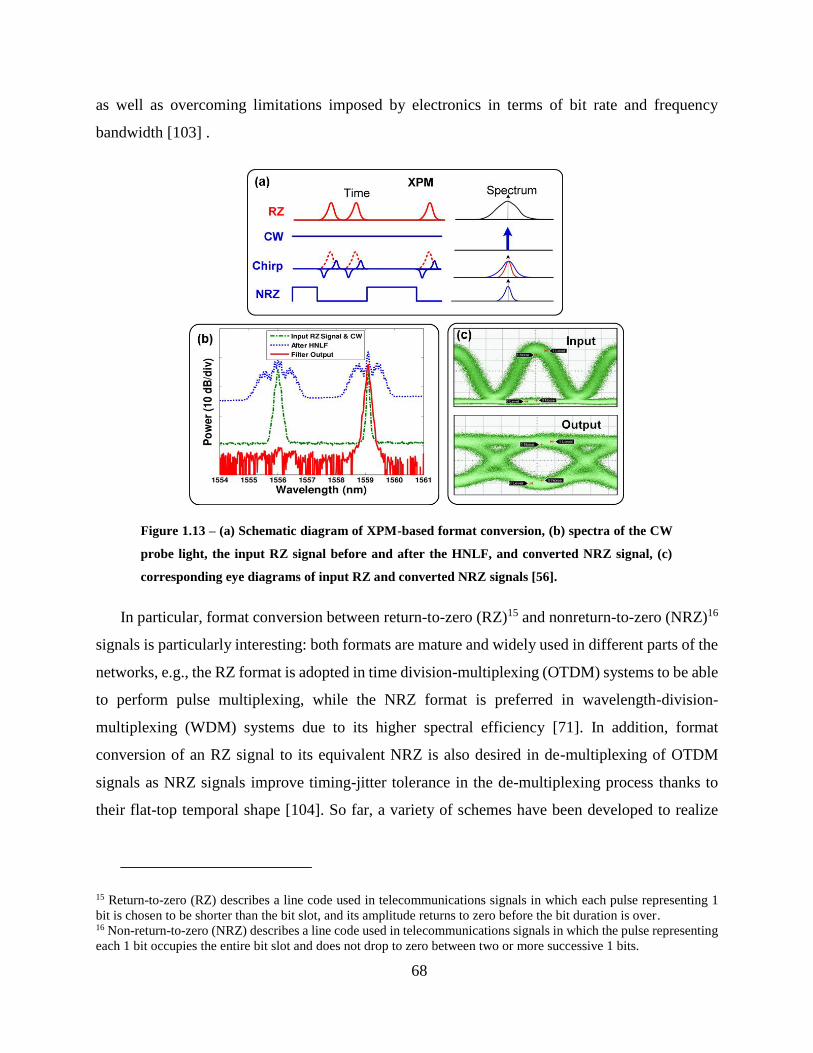
68
as well as overcoming limitations imposed by electronics in terms of bit rate and frequency
bandwidth [103] .
Figure 1.13 – (a) Schematic diagram of XPM-based format conversion, (b) spectra of the CW
probe light, the input RZ signal before and after the HNLF, and converted NRZ signal, (c)
corresponding eye diagrams of input RZ and converted NRZ signals [56].
In particular, format conversion between return-to-zero (RZ)15 and nonreturn-to-zero (NRZ)16
signals is particularly interesting: both formats are mature and widely used in different parts of the
networks, e.g., the RZ format is adopted in time division-multiplexing (OTDM) systems to be able
to perform pulse multiplexing, while the NRZ format is preferred in wavelength-division-
multiplexing (WDM) systems due to its higher spectral efficiency [71]. In addition, format
conversion of an RZ signal to its equivalent NRZ is also desired in de-multiplexing of OTDM
signals as NRZ signals improve timing-jitter tolerance in the de-multiplexing process thanks to
their flat-top temporal shape [104]. So far, a variety of schemes have been developed to realize
15 Return-to-zero (RZ) describes a line code used in telecommunications signals in which each pulse representing 1
bit is chosen to be shorter than the bit slot, and its amplitude returns to zero before the bit duration is over. 16 Non-return-to-zero (NRZ) describes a line code used in telecommunications signals in which the pulse representing
each 1 bit occupies the entire bit slot and does not drop to zero between two or more successive 1 bits.
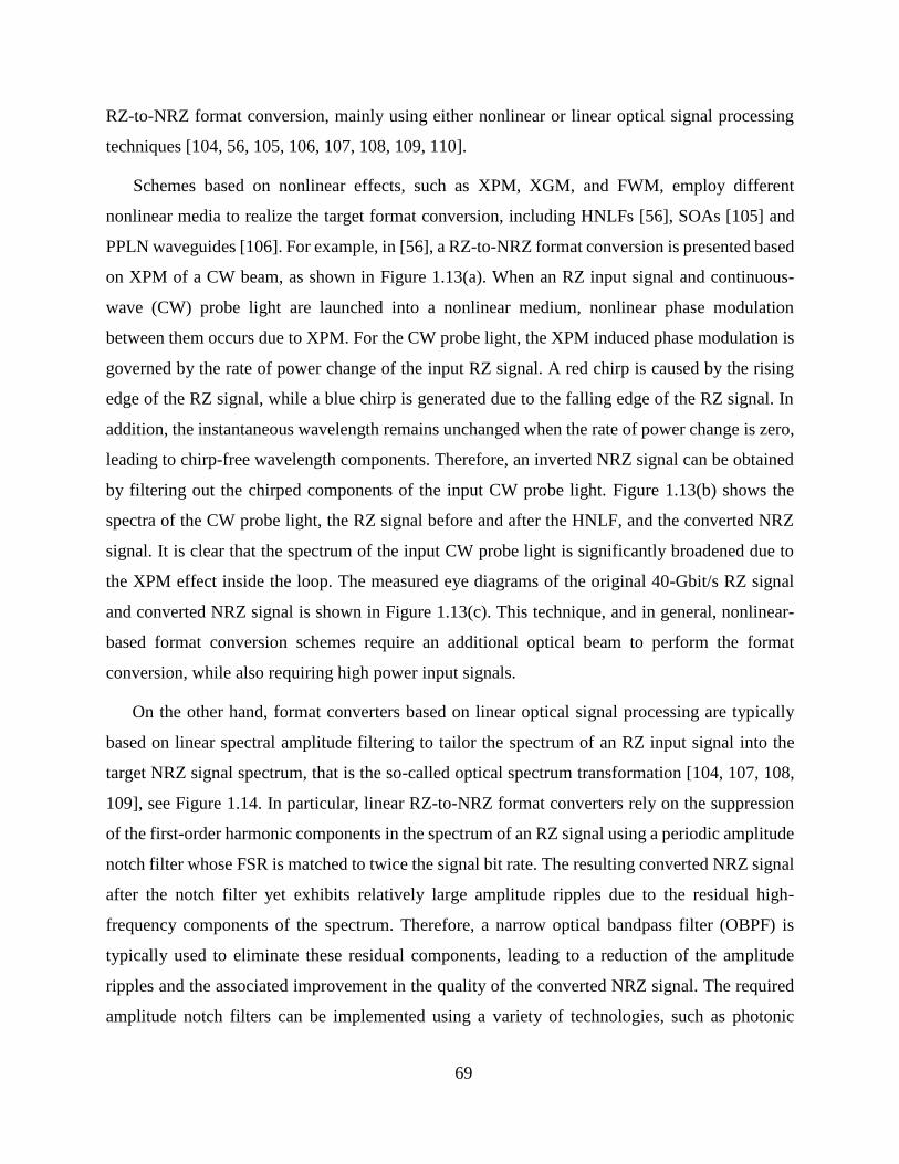
69
RZ-to-NRZ format conversion, mainly using either nonlinear or linear optical signal processing
techniques [104, 56, 105, 106, 107, 108, 109, 110].
Schemes based on nonlinear effects, such as XPM, XGM, and FWM, employ different
nonlinear media to realize the target format conversion, including HNLFs [56], SOAs [105] and
PPLN waveguides [106]. For example, in [56], a RZ-to-NRZ format conversion is presented based
on XPM of a CW beam, as shown in Figure 1.13(a). When an RZ input signal and continuous-
wave (CW) probe light are launched into a nonlinear medium, nonlinear phase modulation
between them occurs due to XPM. For the CW probe light, the XPM induced phase modulation is
governed by the rate of power change of the input RZ signal. A red chirp is caused by the rising
edge of the RZ signal, while a blue chirp is generated due to the falling edge of the RZ signal. In
addition, the instantaneous wavelength remains unchanged when the rate of power change is zero,
leading to chirp-free wavelength components. Therefore, an inverted NRZ signal can be obtained
by filtering out the chirped components of the input CW probe light. Figure 1.13(b) shows the
spectra of the CW probe light, the RZ signal before and after the HNLF, and the converted NRZ
signal. It is clear that the spectrum of the input CW probe light is significantly broadened due to
the XPM effect inside the loop. The measured eye diagrams of the original 40-Gbit/s RZ signal
and converted NRZ signal is shown in Figure 1.13(c). This technique, and in general, nonlinear-
based format conversion schemes require an additional optical beam to perform the format
conversion, while also requiring high power input signals.
On the other hand, format converters based on linear optical signal processing are typically
based on linear spectral amplitude filtering to tailor the spectrum of an RZ input signal into the
target NRZ signal spectrum, that is the so-called optical spectrum transformation [104, 107, 108,
109], see Figure 1.14. In particular, linear RZ-to-NRZ format converters rely on the suppression
of the first-order harmonic components in the spectrum of an RZ signal using a periodic amplitude
notch filter whose FSR is matched to twice the signal bit rate. The resulting converted NRZ signal
after the notch filter yet exhibits relatively large amplitude ripples due to the residual high-
frequency components of the spectrum. Therefore, a narrow optical bandpass filter (OBPF) is
typically used to eliminate these residual components, leading to a reduction of the amplitude
ripples and the associated improvement in the quality of the converted NRZ signal. The required
amplitude notch filters can be implemented using a variety of technologies, such as photonic
70
microring resonators [104, 107, 108], interferometers [109], and fiber Bragg gratings (FBGs)
[110].
Figure 1.14 – Spectra (top row) and temporal waveforms (bottom row) evolution of format
conversion from RZ to NRZ based on optical spectrum transformation. f: frequency, t: time.
Linear format conversion platforms are of greater interest due to their intrinsic simplicity,
suitability for high speed operation and stable performance. In addition, unlike nonlinear-based
schemes, linear converters do not require any additional optical beam to perform the format
conversion while also avoiding the need for high power input signals, as required otherwise to
excite optical nonlinear effects.
1.3.3 Optical picosecond pulse generation methods for high-speed optical systems
Picosecond optical pulse trains in the gigahertz (GHz) regime and beyond are of fundamental
interest for a very wide range of applications in the fields of fiber optics communications [111],
optical computing [112], microwave photonics [113], material processing [114], frequency combs
[115], nonlinear optics [116] and so on. In particular, in the context of optical communications,
OTDM systems require stable high repetition-rate optical pulse sources which can act both as a
data transmission source, and as an optical clock used to synchronize the signal and extract the
transmitted information. Temporal synchronization is also of great importance in optical signal
71
processors including regenerators and logic circuits [112, 44] . In order to ensure synchronization
in an optical signal processing circuit, a single reference optical clock, i.e., a high repetition-rate
pulse train, may be used throughout the circuit. Optical circuits are likely to consist of a number
of fast operations, synchronized to each other, but running at different rates depending on the
function that they perform. The central optical processing units may be expected to run at a
reference rate, while optical processing units in the periphery of the optical circuit may be run at
significantly higher or lower rates. Therefore, a reliable high repetition-rate optical pulse source
with the possibility of programming the repetition-rate from several GHz to hundreds of GHz is
required.
Another potential field of application for high speed optical pulse source is the microwave
photonics— the interface between optical components and devices whose operating spectrum
(frequency) resides well within and above the microwave range. [113]. Certain electronic systems
may require ultrahigh sampling rates in analog-to-digital converters [117]. In this context, optical
pulses can be used to generate short burst of electrons, which subsequently act as a sampling pulse
train in the sub-THz range.
Amongst many desirable characteristic of a high repetition-rate optical source used at the
aforementioned applications, one can include pulse stability, low timing jitter, and low amplitude
fluctuations, especially for applications using a pulse train as a reference or sampling clock signal.
A large number of short pulse, high repetition-rate laser sources have been demonstrated so
far. Ultrafast fiber lasers offer an immediate and attractive platform for generation of high
repetitive pulse trains [118]. In early demonstrations aimed at achieving high repetition-rate pulse
sources, actively mode-locking schemes have been used, with demonstrated repetition-rates up to
~40GHz. However, a further increase of the repetition-rate is limited by the available electrical
bandwidth of the modulator and its driving electronics. Previously, various approaches have been
explored to generate high repetition-rate pulses both from passively and actively mode-locked
fiber lasers, using mechanisms that enable overcoming electrical bandwidth limitations [118].
However, though impressive results have been demonstrated using these approaches, they
typically require a precise control of the optical properties of the laser cavity and they offer very
limited flexibility to program or tune the output repetition-rates. This precludes the potential use
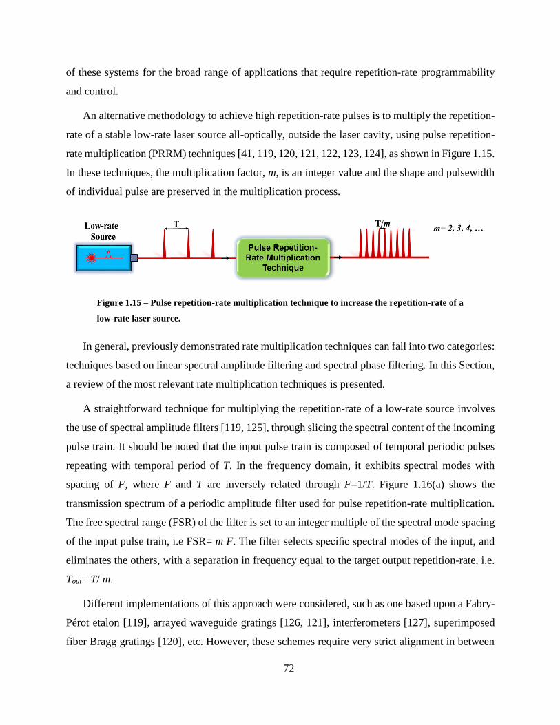
72
of these systems for the broad range of applications that require repetition-rate programmability
and control.
An alternative methodology to achieve high repetition-rate pulses is to multiply the repetition-
rate of a stable low-rate laser source all-optically, outside the laser cavity, using pulse repetition-
rate multiplication (PRRM) techniques [41, 119, 120, 121, 122, 123, 124], as shown in Figure 1.15.
In these techniques, the multiplication factor, m, is an integer value and the shape and pulsewidth
of individual pulse are preserved in the multiplication process.
Figure 1.15 – Pulse repetition-rate multiplication technique to increase the repetition-rate of a
low-rate laser source.
In general, previously demonstrated rate multiplication techniques can fall into two categories:
techniques based on linear spectral amplitude filtering and spectral phase filtering. In this Section,
a review of the most relevant rate multiplication techniques is presented.
A straightforward technique for multiplying the repetition-rate of a low-rate source involves
the use of spectral amplitude filters [119, 125], through slicing the spectral content of the incoming
pulse train. It should be noted that the input pulse train is composed of temporal periodic pulses
repeating with temporal period of T. In the frequency domain, it exhibits spectral modes with
spacing of F, where F and T are inversely related through F=1/T. Figure 1.16(a) shows the
transmission spectrum of a periodic amplitude filter used for pulse repetition-rate multiplication.
The free spectral range (FSR) of the filter is set to an integer multiple of the spectral mode spacing
of the input pulse train, i.e FSR= m F. The filter selects specific spectral modes of the input, and
eliminates the others, with a separation in frequency equal to the target output repetition-rate, i.e.
Tout= T/ m.
Different implementations of this approach were considered, such as one based upon a Fabry-
Pérot etalon [119], arrayed waveguide gratings [126, 121], interferometers [127], superimposed
fiber Bragg gratings [120], etc. However, these schemes require very strict alignment in between
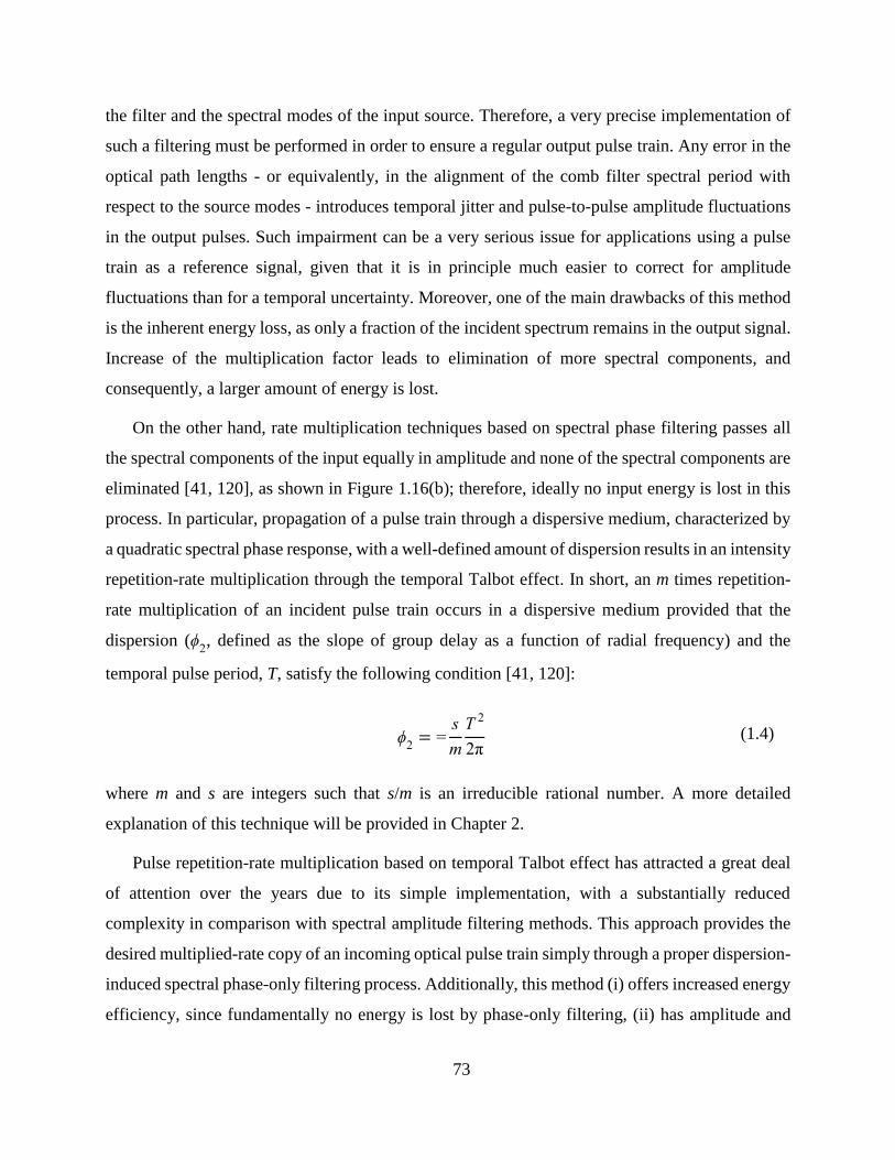
73
the filter and the spectral modes of the input source. Therefore, a very precise implementation of
such a filtering must be performed in order to ensure a regular output pulse train. Any error in the
optical path lengths - or equivalently, in the alignment of the comb filter spectral period with
respect to the source modes - introduces temporal jitter and pulse-to-pulse amplitude fluctuations
in the output pulses. Such impairment can be a very serious issue for applications using a pulse
train as a reference signal, given that it is in principle much easier to correct for amplitude
fluctuations than for a temporal uncertainty. Moreover, one of the main drawbacks of this method
is the inherent energy loss, as only a fraction of the incident spectrum remains in the output signal.
Increase of the multiplication factor leads to elimination of more spectral components, and
consequently, a larger amount of energy is lost.
On the other hand, rate multiplication techniques based on spectral phase filtering passes all
the spectral components of the input equally in amplitude and none of the spectral components are
eliminated [41, 120], as shown in Figure 1.16(b); therefore, ideally no input energy is lost in this
process. In particular, propagation of a pulse train through a dispersive medium, characterized by
a quadratic spectral phase response, with a well-defined amount of dispersion results in an intensity
repetition-rate multiplication through the temporal Talbot effect. In short, an m times repetition-
rate multiplication of an incident pulse train occurs in a dispersive medium provided that the
dispersion (ϕ2
, defined as the slope of group delay as a function of radial frequency) and the
temporal pulse period, T, satisfy the following condition [41, 120]:
ϕ2
= =s
m
T 2
2π (1.4)
where m and s are integers such that s/m is an irreducible rational number. A more detailed
explanation of this technique will be provided in Chapter 2.
Pulse repetition-rate multiplication based on temporal Talbot effect has attracted a great deal
of attention over the years due to its simple implementation, with a substantially reduced
complexity in comparison with spectral amplitude filtering methods. This approach provides the
desired multiplied-rate copy of an incoming optical pulse train simply through a proper dispersion-
induced spectral phase-only filtering process. Additionally, this method (i) offers increased energy
efficiency, since fundamentally no energy is lost by phase-only filtering, (ii) has amplitude and
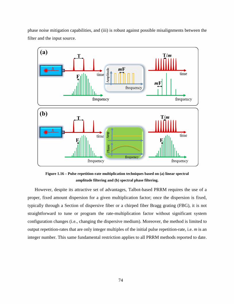
74
phase noise mitigation capabilities, and (iii) is robust against possible misalignments between the
filter and the input source.
Figure 1.16 – Pulse repetition-rate multiplication techniques based on (a) linear spectral
amplitude filtering and (b) spectral phase filtering.
However, despite its attractive set of advantages, Talbot-based PRRM requires the use of a
proper, fixed amount dispersion for a given multiplication factor; once the dispersion is fixed,
typically through a Section of dispersive fiber or a chirped fiber Bragg grating (FBG), it is not
straightforward to tune or program the rate-multiplication factor without significant system
configuration changes (i.e., changing the dispersive medium). Moreover, the method is limited to
output repetition-rates that are only integer multiples of the initial pulse repetition-rate, i.e. m is an
integer number. This same fundamental restriction applies to all PRRM methods reported to date.

75
1.4 Objective and Organization of the Thesis
Energy consumption, and the associated thermal issues, have been a driving consideration
behind much of the progress made by the electronic industry over the past half century. In
comparison, the optical signal processing research community has paid scant attention to the
question of energy consumption. It is often argued that optical signal processing will replace digital
signal processing because of its high-speed capabilities. However, simplistic arguments based on
speed alone often miss the critically important point that optical devices are generally very energy
hungry. Unless there are many-orders-of-magnitude improvement in the energy efficiency of
optical processors, electronics is likely to remain the technology of choice for the vast majority of
signal processing and switching applications in telecommunication networks.
A key objective of this dissertation is to highlight the importance of energy consumption as a
measure of performance in optical signal processing and to try to provide a technological solution
to the problem of energy consumption in relevant optical processors. In particular, in this
dissertation, we explore the possibility of using energy-efficient, passive/active linear techniques
for optical signal processing, avoiding the use of conventional energy-hungry optical active and/or
nonlinear mechanisms; we choose a linear active temporal modulation scheme, i.e., electro-optic
modulation, that provides the simplest and most energy-efficient (i.e., the lowest consuming
energy) mechanism for temporal modulation of an optical signal. In particular, we introduce novel
concepts and innovative approaches for implementation of important signal-processing operations
using temporal phase modulation and/or spectral phase filtering processes that inherently preserve
the entire input signal energy without requiring additional light sources. Through these concepts,
the incoming signal’s energy is effectively redistributed to build up the target output signal without
energy loss and without using any additional external optical power.
This dissertation is mainly focused on optical signal processing of periodic and aperiodic (data)
signals. Figure 1.17 shows a summary of the proposed functionalities in these two categories in
my PhD research program.
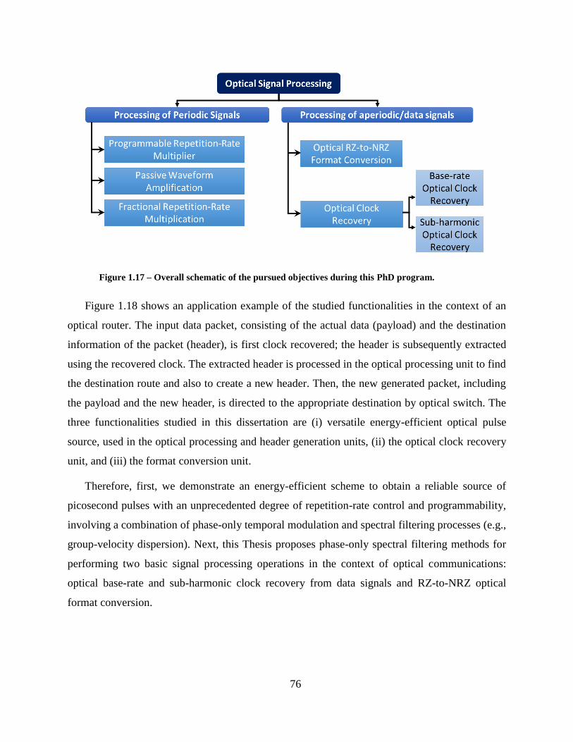
76
Figure 1.17 – Overall schematic of the pursued objectives during this PhD program.
Figure 1.18 shows an application example of the studied functionalities in the context of an
optical router. The input data packet, consisting of the actual data (payload) and the destination
information of the packet (header), is first clock recovered; the header is subsequently extracted
using the recovered clock. The extracted header is processed in the optical processing unit to find
the destination route and also to create a new header. Then, the new generated packet, including
the payload and the new header, is directed to the appropriate destination by optical switch. The
three functionalities studied in this dissertation are (i) versatile energy-efficient optical pulse
source, used in the optical processing and header generation units, (ii) the optical clock recovery
unit, and (iii) the format conversion unit.
Therefore, first, we demonstrate an energy-efficient scheme to obtain a reliable source of
picosecond pulses with an unprecedented degree of repetition-rate control and programmability,
involving a combination of phase-only temporal modulation and spectral filtering processes (e.g.,
group-velocity dispersion). Next, this Thesis proposes phase-only spectral filtering methods for
performing two basic signal processing operations in the context of optical communications:
optical base-rate and sub-harmonic clock recovery from data signals and RZ-to-NRZ optical
format conversion.
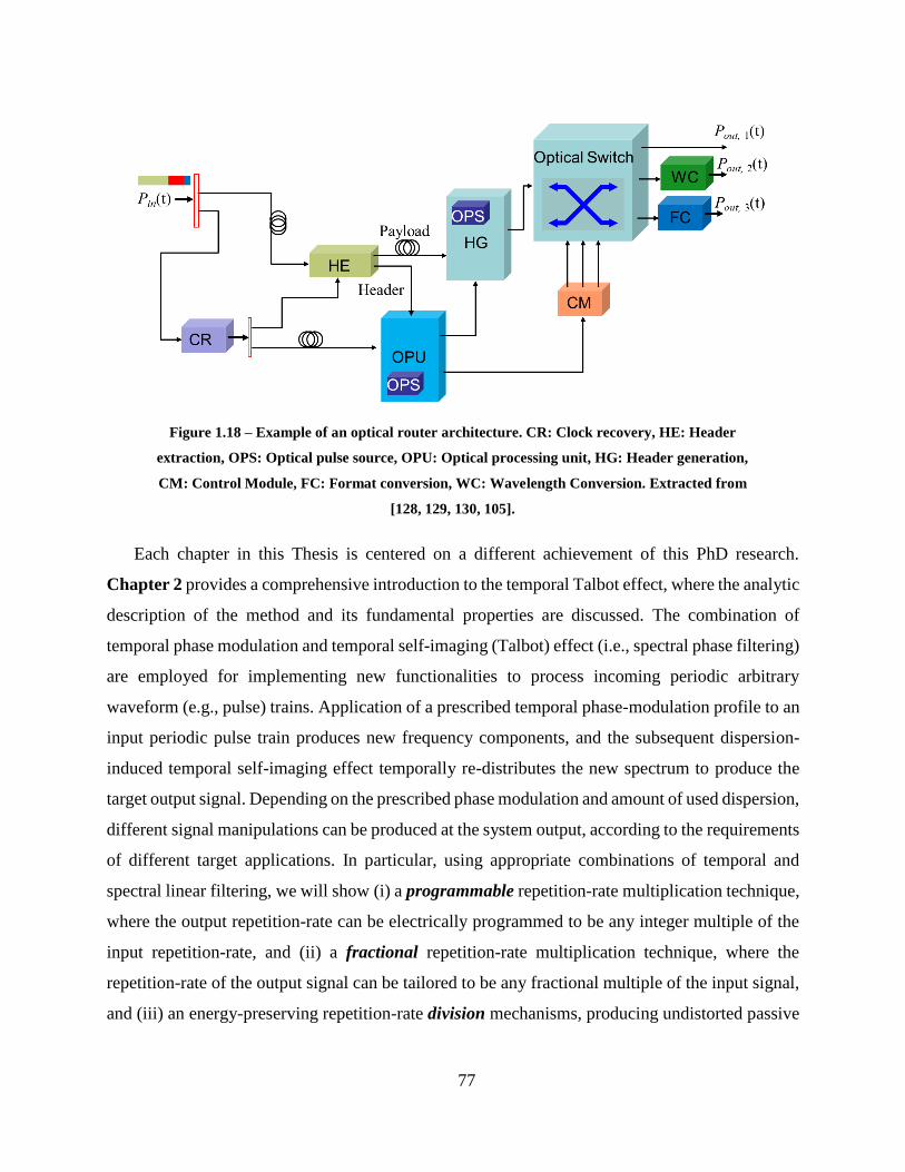
77
Figure 1.18 – Example of an optical router architecture. CR: Clock recovery, HE: Header
extraction, OPS: Optical pulse source, OPU: Optical processing unit, HG: Header generation,
CM: Control Module, FC: Format conversion, WC: Wavelength Conversion. Extracted from
[128, 129, 130, 105].
Each chapter in this Thesis is centered on a different achievement of this PhD research.
Chapter 2 provides a comprehensive introduction to the temporal Talbot effect, where the analytic
description of the method and its fundamental properties are discussed. The combination of
temporal phase modulation and temporal self-imaging (Talbot) effect (i.e., spectral phase filtering)
are employed for implementing new functionalities to process incoming periodic arbitrary
waveform (e.g., pulse) trains. Application of a prescribed temporal phase-modulation profile to an
input periodic pulse train produces new frequency components, and the subsequent dispersion-
induced temporal self-imaging effect temporally re-distributes the new spectrum to produce the
target output signal. Depending on the prescribed phase modulation and amount of used dispersion,
different signal manipulations can be produced at the system output, according to the requirements
of different target applications. In particular, using appropriate combinations of temporal and
spectral linear filtering, we will show (i) a programmable repetition-rate multiplication technique,
where the output repetition-rate can be electrically programmed to be any integer multiple of the
input repetition-rate, and (ii) a fractional repetition-rate multiplication technique, where the
repetition-rate of the output signal can be tailored to be any fractional multiple of the input signal,
and (iii) an energy-preserving repetition-rate division mechanisms, producing undistorted passive
78
amplification of each resulting individual waveform, i.e. a passive waveform amplifier without
using active gain.
Chapter 3 introduces novel energy-efficient signal processing concepts and technologies for
optical data signals. For this purpose, we define, design, and develop two relevant set of
processors: (i) A novel approach for all optical return-to-zero (RZ)-to-non-RZ (NRZ)
telecommunication data format conversion, which has been experimentally implemented at a bit
rate of 640 Gbit/s. In this approach, we show how a proper phase-only manipulation of the
frequency content of a RZ data signal can be used to implement conversion of the RZ signal into
the equivalent NRZ time-domain data. (ii) Novel approaches for base-rate and sub-harmonic clock
recovery from on-off-keying (OOK) data signals. The former is implemented based on phase-only
linear optical filtering of the incoming RZ signal whereas the latter exploits the so-called ‘inverse’
self-imaging effect.
Chapter 4 summarizes the work presented in this Thesis and proposes potential prospects for
future work.
79
Chapter 2
2 Energy-preserving pulse repetition-
rate control for high-speed optical
systems
2.1 Introduction
The Talbot (self-imaging) effect, also referred to as lensless imaging, is a concept with a
distinguished pedigree. The Talbot effect is a Fresnel (near-field) diffraction effect in which
incident plane waves on a periodic structure produce self-images or Talbot revivals. This effect
was originally discovered by Talbot more than 170 years ago [131]. Over the years, investigators
have come to understand different aspects of this phenomenon, and a theory of the Talbot effect
based upon classical diffraction theory has emerged that is capable of explaining various
observations. Additionally, in the framework of the space-time duality, the temporal analog of the
Talbot effect was first described in 1981 (about 35 years ago) [132] by propagating a periodic
temporal signal (for instance, a stream of short optical pulses) through a dispersive medium under
first-order dispersion conditions. Since then, the temporal Talbot effect has attracted considerable
interest and has found various applications [133, 41, 134, 135, 136, 137].
In this Chapter, we use the temporal Talbot effect as the basis of our proposed concepts and
methods for generation and repetition-rate control of picosecond pulse trains. As such, we first
provide an overview of the fundamentals of the temporal Talbot self-imaging effect (Section 2.2).
Next, this effect has been successfully employed for the design and realization of (i) a
programmable repet-ition-rate multiplication technique, where the output repetition-rate can be
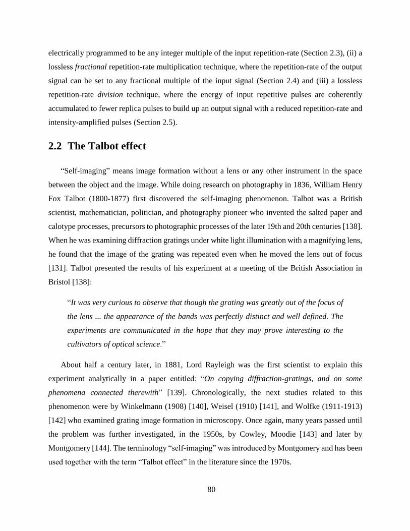
80
electrically programmed to be any integer multiple of the input repetition-rate (Section 2.3), (ii) a
lossless fractional repetition-rate multiplication technique, where the repetition-rate of the output
signal can be set to any fractional multiple of the input signal (Section 2.4) and (iii) a lossless
repetition-rate division technique, where the energy of input repetitive pulses are coherently
accumulated to fewer replica pulses to build up an output signal with a reduced repetition-rate and
intensity-amplified pulses (Section 2.5).
2.2 The Talbot effect
“Self-imaging” means image formation without a lens or any other instrument in the space
between the object and the image. While doing research on photography in 1836, William Henry
Fox Talbot (1800-1877) first discovered the self-imaging phenomenon. Talbot was a British
scientist, mathematician, politician, and photography pioneer who invented the salted paper and
calotype processes, precursors to photographic processes of the later 19th and 20th centuries [138].
When he was examining diffraction gratings under white light illumination with a magnifying lens,
he found that the image of the grating was repeated even when he moved the lens out of focus
[131]. Talbot presented the results of his experiment at a meeting of the British Association in
Bristol [138]:
“It was very curious to observe that though the grating was greatly out of the focus of
the lens ... the appearance of the bands was perfectly distinct and well defined. The
experiments are communicated in the hope that they may prove interesting to the
cultivators of optical science.”
About half a century later, in 1881, Lord Rayleigh was the first scientist to explain this
experiment analytically in a paper entitled: “On copying diffraction-gratings, and on some
phenomena connected therewith” [139]. Chronologically, the next studies related to this
phenomenon were by Winkelmann (1908) [140], Weisel (1910) [141], and Wolfke (1911-1913)
[142] who examined grating image formation in microscopy. Once again, many years passed until
the problem was further investigated, in the 1950s, by Cowley, Moodie [143] and later by
Montgomery [144]. The terminology “self-imaging” was introduced by Montgomery and has been
used together with the term “Talbot effect” in the literature since the 1970s.
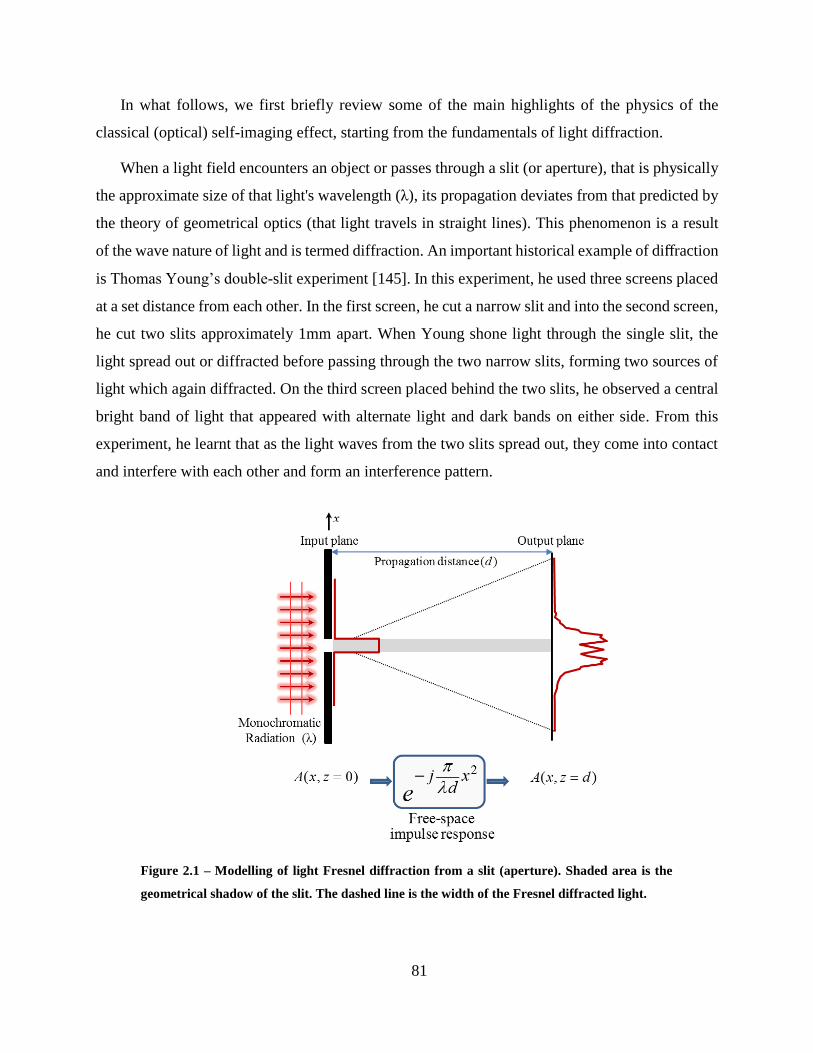
81
In what follows, we first briefly review some of the main highlights of the physics of the
classical (optical) self-imaging effect, starting from the fundamentals of light diffraction.
When a light field encounters an object or passes through a slit (or aperture), that is physically
the approximate size of that light's wavelength (λ), its propagation deviates from that predicted by
the theory of geometrical optics (that light travels in straight lines). This phenomenon is a result
of the wave nature of light and is termed diffraction. An important historical example of diffraction
is Thomas Young’s double-slit experiment [145]. In this experiment, he used three screens placed
at a set distance from each other. In the first screen, he cut a narrow slit and into the second screen,
he cut two slits approximately 1mm apart. When Young shone light through the single slit, the
light spread out or diffracted before passing through the two narrow slits, forming two sources of
light which again diffracted. On the third screen placed behind the two slits, he observed a central
bright band of light that appeared with alternate light and dark bands on either side. From this
experiment, he learnt that as the light waves from the two slits spread out, they come into contact
and interfere with each other and form an interference pattern.
Figure 2.1 – Modelling of light Fresnel diffraction from a slit (aperture). Shaded area is the
geometrical shadow of the slit. The dashed line is the width of the Fresnel diffracted light.

82
As detailed in classic treatments, the calculation of the light field immediately behind the
diffracting object or slit is a subject of great interest. Figure 2.1 shows a slit (aperture) at the input
plane illuminated by a plane-wavefront monochromatic light, and the resulting light diffraction at
the output plane behind the slit, with an x-z coordinate system where z is the optical propagation
axis and x is the transverse axis. For simplicity, only one transverse dimension is assumed, x-axis,
but the same behavior would be observed in the y-axis. The dynamics of the complex amplitude
of the light field behind the diffracting object A(x,z=0) (at the input plane) is described by the wave
equation approximation:
∂A
∂z=
i
2 k
∂2A
∂x2 (2.1)
where k=2π/λ is the propagation constant with λ being the light wavelength. Under the so-called
Fresnel approximation, this equation can be solved by the well-known Fresnel diffraction integral
[146, 147]. Mathematically, this integral can be also modelled as the convolution of the complex
amplitude function of the diffracting object A(x,z=0) and the impulse response of light propagation
in free space (sometimes called the impulse response of free space), displaying a rich set of
properties associated with general linear systems [147]. This description of light propagation in
free space, by an impulse response, implies that the diffraction imaging system is linear and shift
invariant. The amplitude impulse response of light propagation in free space is an expanding
quadratic-phase function [41]:
ℎ̃d(x) ∝ exp (-jk
2d x2) (2.2)
where z = d is the propagation distance (at the output plane) from the input plane. Figure 2.1 shows
the diffraction pattern at the distance d from the illuminated slit: The intensity of the light field just
behind the slit (|A(x,z=0)|2) and at a distance d away from the input plane (|A(x,z=d)|2) (i.e., the
diffraction pattern) are displayed as a function of the transverse position (x-axis) in the input and
output planes, respectively. As mentioned above, the resulting diffraction pattern can be predicted
by convolving the input field amplitude A(x,z=0) with the impulse response function of light
propagation ℎ̃d(x) (Eq. (2.2)).
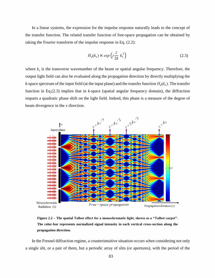
83
In a linear systems, the expression for the impulse response naturally leads to the concept of
the transfer function. The related transfer function of free-space propagation can be obtained by
taking the Fourier transform of the impulse response in Eq. (2.2):
Hd(kx) ∝ exp (jz
2k kx
2) (2.3)
where kx is the transverse wavenumber of the beam or spatial angular frequency. Therefore, the
output light field can also be evaluated along the propagation direction by directly multiplying the
k-space spectrum of the input field (at the input plane) and the transfer function Hd(kx). The transfer
function in Eq.(2.3) implies that in k-space (spatial angular frequency domain), the diffraction
imparts a quadratic phase shift on the light field. Indeed, this phase is a measure of the degree of
beam divergence in the x direction.
Figure 2.2 – The spatial Talbot effect for a monochromatic light, shown as a “Talbot carpet”.
The color-bar represents normalized signal intensity in each vertical cross-section along the
propagation direction.
In the Fresnel diffraction regime, a counterintuitive situation occurs when considering not only
a single slit, or a pair of them, but a periodic array of slits (or apertures), with the period of the
84
array Λ in the input plane, each contributing to the diffraction pattern. This is for instance the case
for a spatial diffraction grating, illuminated by a monochromatic light beam. By using Fresnel
diffraction theory, Eq.(2.2), one can still evaluate the transverse field amplitude along the direction
of propagation z. Figure 2.2 shows the resulting diffraction pattern behind the input plane.
Interestingly, we find that the original periodic pattern is reproduced exactly behind the input plane
at distances z = d:
d= sΛ
2
λ (2.4)
where s = 2, 4, 6, … (even integers), a formula first derived by Lord Rayleigh in 1881 [139]. This
is the basic “Talbot” or “self-imaging” effect. At distances, satisfying Eq.(2.4), but for s = 1, 3, 5,
… (odd integers), we find that the original pattern is also reproduced, but with a half-period (Λ/2)
shift. Originally, the Talbot effect was only described for this basic situation according to which
the field reproduces itself when z is a multiple of the so-called Talbot distance (dΛ = Λ2/λ). This
is what is known as the integer Talbot effect.
In addition to the described reconstruction images, there also exists another set of distances
where one finds other interesting diffraction patterns, Figure 2.2. At positions z = d, such that
d=s
mdΛ =
s
m
Λ2
λ (2.5)
with s = 1, 2, 3, … and m = 2, 3, 4,…, such that (s/m) is a noninteger and irreducible rational
number, the original periodic pattern reappears, but with a periodicity of Λ/m. This sub-images
were first identified by Winthrop and Worthington [148], and this effect now is known as the
fractional or sub-Talbot effect. For example, at distances z = dΛ/3 and z = dΛ/2, the periodicity of
the original pattern (in the input plane) is reduced by factors of m = 2 (to Λ/2) and m = 3 (to Λ/3),
respectively. Visualization of the intriguing wave patterns behind a periodic array of slits (such as
a diffraction grating ) due to Talbot effect is referred to as the “Talbot carpet”, resembling a Persian
rug in intricate but repeating patterns, as shown in Figure 2.2. A picture of the Talbot carpet is
displayed in the header of the Nature Physics website.
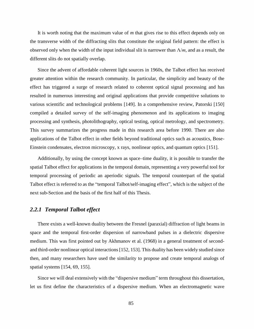
85
It is worth noting that the maximum value of m that gives rise to this effect depends only on
the transverse width of the diffracting slits that constitute the original field pattern: the effect is
observed only when the width of the input individual slit is narrower than Λ/m, and as a result, the
different slits do not spatially overlap.
Since the advent of affordable coherent light sources in 1960s, the Talbot effect has received
greater attention within the research community. In particular, the simplicity and beauty of the
effect has triggered a surge of research related to coherent optical signal processing and has
resulted in numerous interesting and original applications that provide competitive solutions to
various scientific and technological problems [149]. In a comprehensive review, Patorski [150]
compiled a detailed survey of the self-imaging phenomenon and its applications to imaging
processing and synthesis, photolithography, optical testing, optical metrology, and spectrometry.
This survey summarizes the progress made in this research area before 1990. There are also
applications of the Talbot effect in other fields beyond traditional optics such as acoustics, Bose-
Einstein condensates, electron microscopy, x rays, nonlinear optics, and quantum optics [151].
Additionally, by using the concept known as space–time duality, it is possible to transfer the
spatial Talbot effect for applications in the temporal domain, representing a very powerful tool for
temporal processing of periodic an aperiodic signals. The temporal counterpart of the spatial
Talbot effect is referred to as the “temporal Talbot/self-imaging effect”, which is the subject of the
next sub-Section and the basis of the first half of this Thesis.
2.2.1 Temporal Talbot effect
There exists a well-known duality between the Fresnel (paraxial) diffraction of light beams in
space and the temporal first-order dispersion of narrowband pulses in a dielectric dispersive
medium. This was first pointed out by Akhmanov et al. (1968) in a general treatment of second-
and third-order nonlinear optical interactions [152, 153]. This duality has been widely studied since
then, and many researchers have used the similarity to propose and create temporal analogs of
spatial systems [154, 69, 155].
Since we will deal extensively with the “dispersive medium” term throughout this dissertation,
let us first define the characteristics of a dispersive medium. When an electromagnetic wave
86
interacts with a dielectric, the medium response, in general, depends on the optical frequency ω.
This property, referred to as chromatic dispersion, manifests through the frequency dependence of
the refractive index n(ω). This dispersion plays a critical role in the problem of propagation of
short optical pulses because different spectral components associated with the pulse travel at
different speeds given by c/n(ω), c being the speed of light in free space, causing pulse broadening,
see Figure 2.3. Mathematically, the effects of dispersion are accounted for by expanding the
propagation constant β(ω)= n(ω) ω/c in a Taylor series [42]. As will be detailed later in this
Section, a dispersive medium can be modeled as an LTI system with a transfer function
H(ω)=|H(ω)| exp(j Φ(ω)), with Φ(ω) = β(ω) × z where z is the propagation distance in the
dispersive medium. The Taylor expansion of β(ω) over a spectral bandwidth Δω around the
frequency ω0 at which the pulse spectrum is centered may be written as
Φ(ω)=dβ(ω)
dω|ω= ω0
(ω- ω0)z + 1
2
d 2
β(ω)
dω2|ω= ω0
(ω- ω0)2z + 1
6
d 3β(ω)
dω3|ω= ω0
(ω-
ω0)3z…= β1(ω- ω0)z +
1
2 β
2(ω- ω0)2z +
1
6 β
3(ω- ω0)3z+…=
ϕ1(ω- ω0)+
1
2ϕ
2(ω- ω0)+
1
6 ϕ
3(ω- ω0)+…
(2.6)
where
ϕm
=βm
z=d
mβ(ω)
dωm|ω= ω0
z (2.7)
In particular, the parameters β1 and β2 are related to the refractive index n(ω) and its derivatives
through the relations
β1=
1
vg
=1
c(n+ω
dn
dω) (2.8)
β2=
1
c(2
dn
dω+ω
d2n
dω2) (2.9)
The first-order term, β1, contains the inverse group velocity, vg, (i.e., the group delay per unit
length) and describes an overall time delay without an effect on the pulse shape. The second-order
87
term parameter, β2, represents dispersion of the group velocity and is responsible for pulse
broadening. This phenomenon is known as group-velocity dispersion (GVD), and β2 is the GVD
parameter.
Figure 2.3 – Characterization of a first-order dispersion medium.
In addition to these two parameters, higher-order parameters also appears in Eq. (2.6). The
coefficient β3 appearing in Eq. (2.6) is called the third-order dispersion (TOD) parameter. Higher-
order dispersive effects can distort ultrashort optical pulses both in the linear and nonlinear
regimes. As the contribution of the higher-order dispersion terms in most typical dielectric media
and structures (e.g., optical fibers) is quite small for picosecond pulses, these terms can be
neglected in our following discussions. In the absence of higher-order dispersive effects, retaining
only the two first terms of the Taylor expansion of the dispersive medium, Φ(ω) is approximated
by a quadratic function, as shown in Figure 2.3. This approximation is referred to as first-order
dispersion approximation, leading to H(ω) having an all-pass amplitude with a quadratic phase
response. Therefore, the group delay of the dispersive medium, defined as τg= dΦ(ω) dω⁄ =
ϕ1+ ϕ
2(ω-ω0), exhibits a linear variation as a function of frequency. A first-order dispersive
medium is characterized by the slope of the group delay as function of ω, ϕ2, referred to as the
first-order dispersion coefficient. As mentioned above, the first-order dispersion coefficient is
related to the GVD parameter β2 through ϕ
2= β
2× z.
Now, going back to the space-time duality, let us consider the temporal analogue of a slit or
aperture. A good representation is provided by a short light pulse in the time domain. The pulse
88
width and shape correspond to the width and shape of the individual slit. The temporal analogue
of diffraction is group velocity dispersion, and the propagation of a pulse with amplitude A(t, z=0)
in a dispersive medium is described by
∂A
∂z=
iβ2
2
∂2A
∂t2 (2.10)
where t = τ - z/vg is the retarded time. As a matter of fact, equations (2.1) and (2.10) are
mathematically equivalent. It is important to note that both equations represent an approximated
form of the wave equation. The paraxial approximation is used in Eq. (2.1), which assumes that
the field amplitude A(x, z) varies slowly with z on the scale of a wavelength, whereas the derivation
of Eq. (2.10) uses the slowly varying envelope approximation, which assumes that the amplitude
A(t, z) varies slowly with z on the scale of an optical cycle. The only difference between diffraction
and dispersion is that the GVD parameter β2 in Eq. (2.10) can be positive or negative, whereas the
propagation constant k in Eq. (2.1) can be only positive. This implies that in the case of diffraction,
the free-space propagation necessarily exhibits a positive wavelength-distance product (λ×z), i.e.,
high spatial frequencies travel faster laterally than low spatial frequencies. In contrast, in case of
group velocity dispersion, a normal dispersive medium (β2 > 0), such as dispersion compensating
fibers, exhibits a positive frequency chirp (β2 z > 0) – low frequencies travel faster than high
frequencies – and an anomalous dispersive medium (β2 < 0), such as conventional single-mode
optical fibers, exhibits a negative group delay (β2 z < 0) – high frequencies travel faster than low
frequencies. The possibility of having positive or negative dispersion adds an important extra
degree of versatility to design and build optical information processors.
The duality between the temporal dynamics of optical waveforms and the spatial evolution of
optical beams is based on the mathematical equivalence between Eqs. (2.1) and (2.10). In
particular, the free-space propagation distance in the spatial-domain light propagation, which
determines by how much a beam is diffracted, is analogous to the total group delay dispersion, ϕ2,
in a dispersive medium.
As mentioned above, in the Fourier domain, the transfer function of free-space diffraction
imparts on the field a quadratic phase shift in k-space. Similarly, in the linear regime, the transfer
function of first-order dispersion imparts a quadratic spectral phase in the frequency domain:
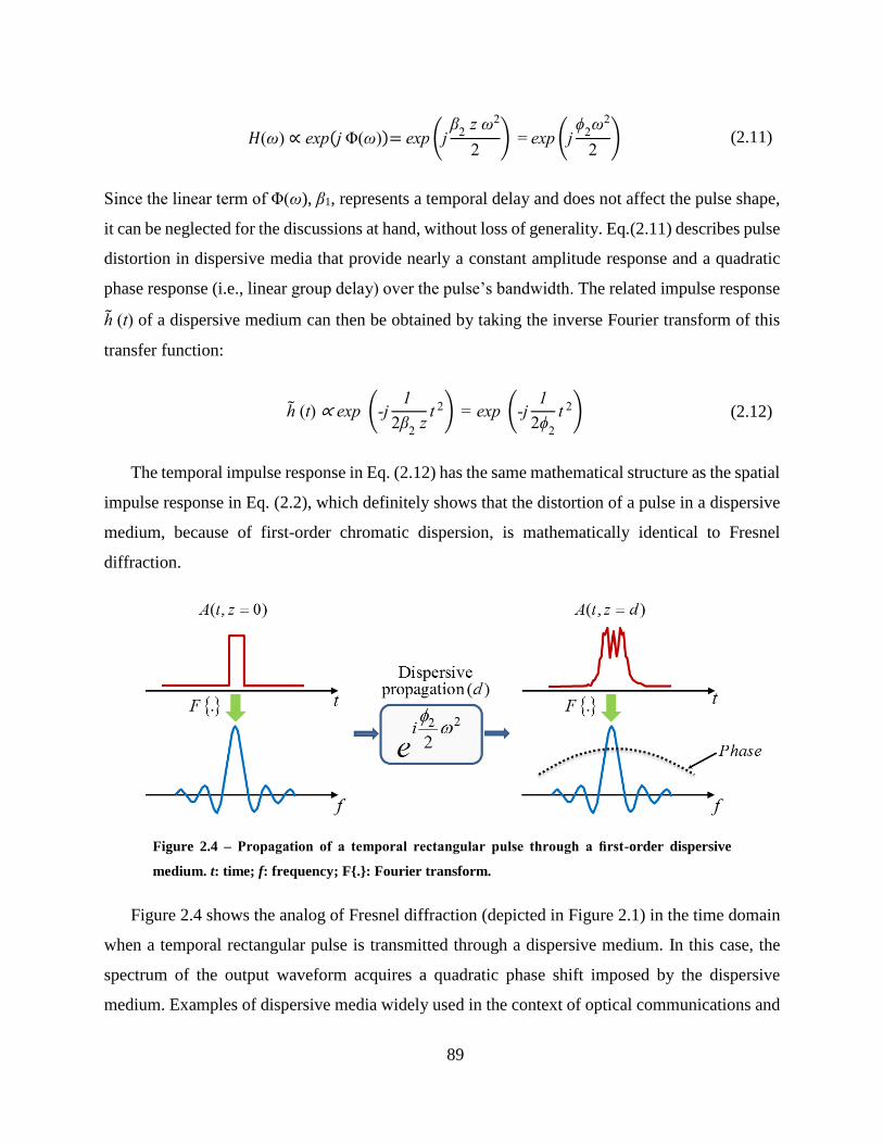
89
𝐻(ω) ∝ exp(j Φ(ω))= exp (jβ
2 z ω2
2) = exp (j
ϕ2ω2
2) (2.11)
Since the linear term of Φ(ω), β1, represents a temporal delay and does not affect the pulse shape,
it can be neglected for the discussions at hand, without loss of generality. Eq.(2.11) describes pulse
distortion in dispersive media that provide nearly a constant amplitude response and a quadratic
phase response (i.e., linear group delay) over the pulse’s bandwidth. The related impulse response
h̃ (t) of a dispersive medium can then be obtained by taking the inverse Fourier transform of this
transfer function:
h̃ (t) ∝ exp (-j1
2β2 z
t 2) = exp (-j1
2ϕ2
t 2) (2.12)
The temporal impulse response in Eq. (2.12) has the same mathematical structure as the spatial
impulse response in Eq. (2.2), which definitely shows that the distortion of a pulse in a dispersive
medium, because of first-order chromatic dispersion, is mathematically identical to Fresnel
diffraction.
Figure 2.4 – Propagation of a temporal rectangular pulse through a first-order dispersive
medium. t: time; f: frequency; F{.}: Fourier transform.
Figure 2.4 shows the analog of Fresnel diffraction (depicted in Figure 2.1) in the time domain
when a temporal rectangular pulse is transmitted through a dispersive medium. In this case, the
spectrum of the output waveform acquires a quadratic phase shift imposed by the dispersive
medium. Examples of dispersive media widely used in the context of optical communications and
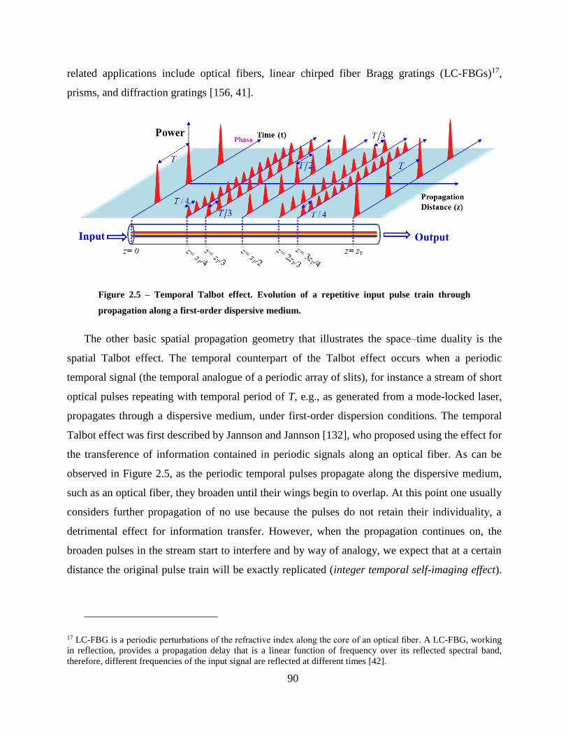
90
related applications include optical fibers, linear chirped fiber Bragg gratings (LC-FBGs)17,
prisms, and diffraction gratings [156, 41].
Figure 2.5 – Temporal Talbot effect. Evolution of a repetitive input pulse train through
propagation along a first-order dispersive medium.
The other basic spatial propagation geometry that illustrates the space–time duality is the
spatial Talbot effect. The temporal counterpart of the Talbot effect occurs when a periodic
temporal signal (the temporal analogue of a periodic array of slits), for instance a stream of short
optical pulses repeating with temporal period of T, e.g., as generated from a mode-locked laser,
propagates through a dispersive medium, under first-order dispersion conditions. The temporal
Talbot effect was first described by Jannson and Jannson [132], who proposed using the effect for
the transference of information contained in periodic signals along an optical fiber. As can be
observed in Figure 2.5, as the periodic temporal pulses propagate along the dispersive medium,
such as an optical fiber, they broaden until their wings begin to overlap. At this point one usually
considers further propagation of no use because the pulses do not retain their individuality, a
detrimental effect for information transfer. However, when the propagation continues on, the
broaden pulses in the stream start to interfere and by way of analogy, we expect that at a certain
distance the original pulse train will be exactly replicated (integer temporal self-imaging effect).
17 LC-FBG is a periodic perturbations of the refractive index along the core of an optical fiber. A LC-FBG, working
in reflection, provides a propagation delay that is a linear function of frequency over its reflected spectral band,
therefore, different frequencies of the input signal are reflected at different times [42].
91
At some other distances, the original pulse sequence reappears but with a repetition-rate that is an
integer multiple of the original one (fractional temporal self-imaging effect).
The derivation of the mathematics of temporal Talbot effects has been covered in deep detail
by Azaña et al (2001) [41]. We briefly review this derivation and conditions for the formation of
temporal Talbot images in a dispersive medium.
Figure 2.5 represents the evolution of an input periodic signal through propagation along a
first-order dispersive medium; here a piece of optical fiber is assumed, where the slope of group
delay increases linearly with the propagation distance, i.e., ϕ2= β
2× z. The complex envelope of
the input periodic signal Ain(t), shown in Figure 2.5 at z = 0 (where z represents the axial
propagation coordinate) can be expressed as
A(t, z=0)= Ain(t) = ∑ a0
∞
p=-∞
(t - pT ) (2.13)
where a0(t) (signal in each period or individual pulse) is an arbitrary complex function in the
interval |t| ≤ T/2, and a0(t) = 0, for |t| > T/2. Obviously, the corresponding average optical power is
also a periodic function, i.e., Pin(t) = | Ain(t) |2 =∑ P0(t-pT)∞
p=-∞ , with P0(t) = | a0(t) |2.
As mentioned above, the linear propagation through a dispersive medium under the first-order
dispersion approximation can be characterized by the spectral transfer function in Eq.(2.11), or the
related temporal impulse response in Eq.(2.12). In this way, the complex envelope Aout(t) of the
output pulse can be obtained by convolving the complex envelope of the input pulse Ain(t) with the
impulse response function Eq.(2.12). Alternatively, one can also operate in the frequency domain:
the output complex envelope spectrum Ȃout(ω)(=ℱ{Aout(t)}) (ℱ represents Fourier transform) can
be obtained by directly multiplying the spectrum of the input complex envelope Ȃin(ω)(=ℱ{Ain(t)})
and the spectral transfer function H(ω) in Eq.(2.11):
Ȃout(ω) = Ȃin(ω)× H(ω) (2.14)
The output signal complex envelope is simply found by taking the inverse Fourier transform
of the output spectrum Aout(t) = ℱ-1{ Ȃout(ω)} (ℱ-1 represents inverse Fourier transform). As
mentioned above, in the chosen dispersive medium, an optical fiber, the dispersion value increases
92
linearly with the propagation distance z (ϕ2= β
2× z) which in turn affects the spectral transfer
function H(ω). Therefore, for different propagation distances, we expect to observe various forms
of output signal. At some specific distances, the original signal is reconstructed (self-imaged)
either with the same or a multiplied repetition-rate. For instance, as shown in Figure 2.5, the input
pulse train is exactly self-imaged after dispersive propagation through an integer multiple of the
Talbot distance (integer Talbot self-images) defined as:
zT=sT 2
2π β2
(2.15)
where s = 1, 2, 3, …. Similar to spatial Talbot effect, for even values of s, we find that the output
signal is an exact replica of the input signal. For odd values of s, we find that the original periodic
signal is also reproduced but with a half-period shift T /2, recall that the time variable ‘t’ is relative
to group delay, therefore, the T/2 delay is in addition to the group delay. In summary, if the
repetition period of the input pulse train verifies condition (2.15), the signal is reproduced without
undergoing distortion. In addition to the described reconstruction images, one finds other
interesting patterns. At fractional distances of:
z =s
mzT=
s
m
T 2
2π β2
(2.16)
with s = 1, 2, 3, …, m = 2, 3, 4, . . ., such that s/m is a noninteger rational number, the output signal
is a copy of the periodic input signal (where an individual pulse maintains its shape and temporal
width), but with a repetition-rate m times that of the input signal. In this case, ideally the individual
pulse power is correspondingly decreased by the factor of m, ignoring the insertion losses of the
dispersive medium. Figure 2.5 shows examples of output pulse trains at the fractional Talbot
distances z = zT /4, zT /3 and zT /2 where the input repetition-rate has been multiplied by factors of
m = 4, 3 and 2, respectively. Note that this rate multiplication process only multiplies the repetition-
rate of the signal's intensity, while the spectrum magnitude remains unchanged, thus leaving a
deterministic pulse-to-pulse residual temporal phase structure on the output pulse train. It is also
worth mentioning that the maximum repetition-rate at the output is only limited to the input pulse
width. The input pulse width must be short enough to prevent pulse overlapping in the multiplied
output train; in particular, assuming that the Talbot condition is satisfied, then m ≤ Dout_max T/tin
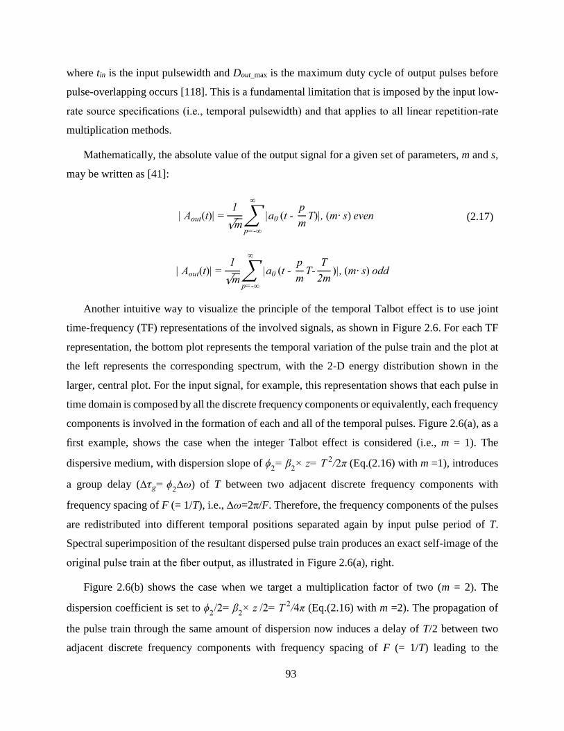
93
where tin is the input pulsewidth and Dout_max is the maximum duty cycle of output pulses before
pulse-overlapping occurs [118]. This is a fundamental limitation that is imposed by the input low-
rate source specifications (i.e., temporal pulsewidth) and that applies to all linear repetition-rate
multiplication methods.
Mathematically, the absolute value of the output signal for a given set of parameters, m and s,
may be written as [41]:
| Aout(t)| =1
√m∑ |a0
∞
p=-∞
(t - p
mT)|, (m· s) even (2.17)
| Aout(t)| =1
√m∑ |a0
∞
p=-∞
(t - p
mT-
T
2m)|, (m· s) odd
Another intuitive way to visualize the principle of the temporal Talbot effect is to use joint
time-frequency (TF) representations of the involved signals, as shown in Figure 2.6. For each TF
representation, the bottom plot represents the temporal variation of the pulse train and the plot at
the left represents the corresponding spectrum, with the 2-D energy distribution shown in the
larger, central plot. For the input signal, for example, this representation shows that each pulse in
time domain is composed by all the discrete frequency components or equivalently, each frequency
components is involved in the formation of each and all of the temporal pulses. Figure 2.6(a), as a
first example, shows the case when the integer Talbot effect is considered (i.e., m = 1). The
dispersive medium, with dispersion slope of ϕ2= β
2× z= T 2/2π (Eq.(2.16) with m =1), introduces
a group delay (∆𝜏g= ϕ2∆ω) of T between two adjacent discrete frequency components with
frequency spacing of F (= 1/T), i.e., Δω=2π/F. Therefore, the frequency components of the pulses
are redistributed into different temporal positions separated again by input pulse period of T.
Spectral superimposition of the resultant dispersed pulse train produces an exact self-image of the
original pulse train at the fiber output, as illustrated in Figure 2.6(a), right.
Figure 2.6(b) shows the case when we target a multiplication factor of two (m = 2). The
dispersion coefficient is set to ϕ2/2= β
2× z /2= T 2/4π (Eq.(2.16) with m =2). The propagation of
the pulse train through the same amount of dispersion now induces a delay of T/2 between two
adjacent discrete frequency components with frequency spacing of F (= 1/T) leading to the
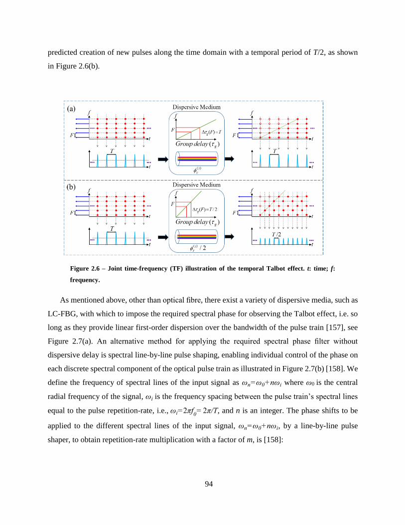
94
predicted creation of new pulses along the time domain with a temporal period of T/2, as shown
in Figure 2.6(b).
Figure 2.6 – Joint time-frequency (TF) illustration of the temporal Talbot effect. t: time; f:
frequency.
As mentioned above, other than optical fibre, there exist a variety of dispersive media, such as
LC-FBG, with which to impose the required spectral phase for observing the Talbot effect, i.e. so
long as they provide linear first-order dispersion over the bandwidth of the pulse train [157], see
Figure 2.7(a). An alternative method for applying the required spectral phase filter without
dispersive delay is spectral line-by-line pulse shaping, enabling individual control of the phase on
each discrete spectral component of the optical pulse train as illustrated in Figure 2.7(b) [158]. We
define the frequency of spectral lines of the input signal as ωn=ω0+nωi where ω0 is the central
radial frequency of the signal, ωi is the frequency spacing between the pulse train’s spectral lines
equal to the pulse repetition-rate, i.e., ωi=2πf0= 2π/T, and n is an integer. The phase shifts to be
applied to the different spectral lines of the input signal, ωn=ω0+nωi, by a line-by-line pulse
shaper, to obtain repetition-rate multiplication with a factor of m, is [158]:
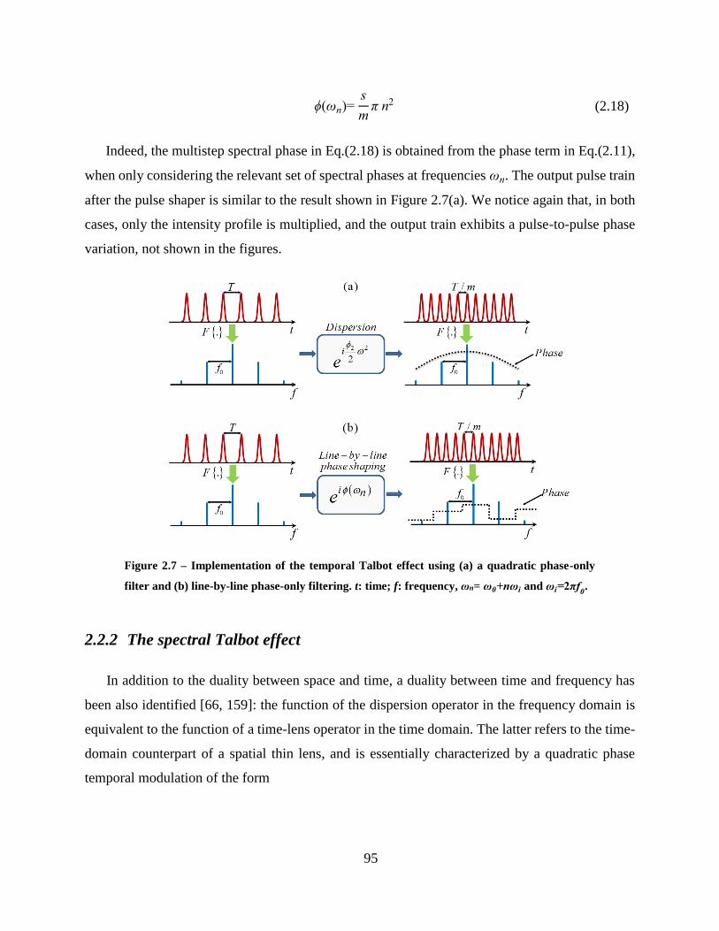
95
ϕ(ωn)=s
mπ n2 (2.18)
Indeed, the multistep spectral phase in Eq.(2.18) is obtained from the phase term in Eq.(2.11),
when only considering the relevant set of spectral phases at frequencies ωn. The output pulse train
after the pulse shaper is similar to the result shown in Figure 2.7(a). We notice again that, in both
cases, only the intensity profile is multiplied, and the output train exhibits a pulse-to-pulse phase
variation, not shown in the figures.
Figure 2.7 – Implementation of the temporal Talbot effect using (a) a quadratic phase-only
filter and (b) line-by-line phase-only filtering. t: time; f: frequency, ωn= ω0+nωi and ωi=2πf0.
2.2.2 The spectral Talbot effect
In addition to the duality between space and time, a duality between time and frequency has
been also identified [66, 159]: the function of the dispersion operator in the frequency domain is
equivalent to the function of a time-lens operator in the time domain. The latter refers to the time-
domain counterpart of a spatial thin lens, and is essentially characterized by a quadratic phase
temporal modulation of the form
96
𝑝(t) ∝ exp (jα
2t2) (2.19)
where α is the linear chirp coefficient of the time-lens process. An important consequence of this
duality is the frequency-domain counterpart of the temporal self-imaging effect, the so-called
spectral self-imaging (Talbot) effect [159]. Spectral self-imaging (Talbot) effect occurs when a
periodic sequence of optical pulses (periodic comb in the frequency domain) is linearly chirped by
a time-lens process. Under specific temporal linear chirping conditions, the input periodic
frequency comb is essentially unaffected by the time lens (integer spectral self-imaging), whereas
for other linear chirping conditions, the free spectral range (FSR) of the frequency comb is divided
by an integer factor (fractional spectral self-imaging), without undergoing any further distortion in
its spectral envelope, as shown in Figure 2.8(a).
Figure 2.8 – Illustration of the spectral Talbot effect (a) using quadratic phase modulation in
the time domain (time lens) and (b) by multilevel time phase modulation. t: time; f: frequency.
The spectral self-imaging condition on the linear chirp coefficient can be obtained from the
frequency-domain analog of the well-established temporal self-imaging theory [41] such that the
needed temporal phase modulation function is:
φ(t)=α
2t2=
s
m
π
T 2 t 2 (2.20)
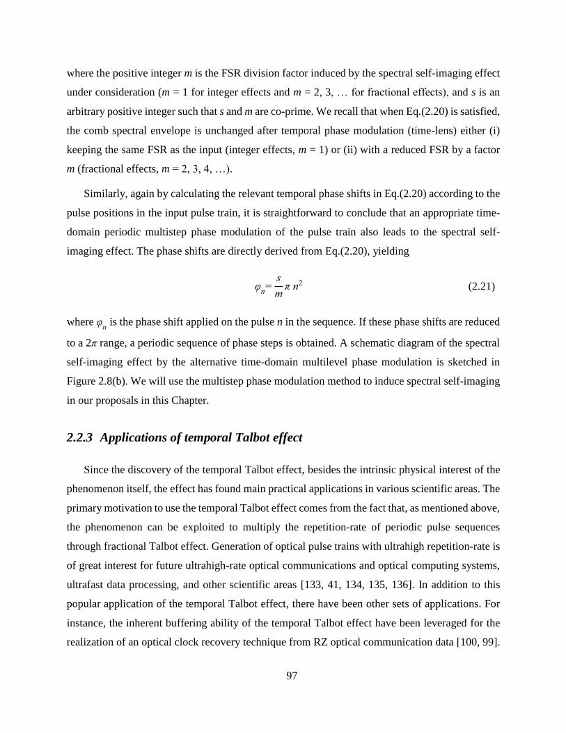
97
where the positive integer m is the FSR division factor induced by the spectral self-imaging effect
under consideration (m = 1 for integer effects and m = 2, 3, … for fractional effects), and s is an
arbitrary positive integer such that s and m are co-prime. We recall that when Eq.(2.20) is satisfied,
the comb spectral envelope is unchanged after temporal phase modulation (time-lens) either (i)
keeping the same FSR as the input (integer effects, m = 1) or (ii) with a reduced FSR by a factor
m (fractional effects, m = 2, 3, 4, …).
Similarly, again by calculating the relevant temporal phase shifts in Eq.(2.20) according to the
pulse positions in the input pulse train, it is straightforward to conclude that an appropriate time-
domain periodic multistep phase modulation of the pulse train also leads to the spectral self-
imaging effect. The phase shifts are directly derived from Eq.(2.20), yielding
φn=
s
mπ n2 (2.21)
where φn is the phase shift applied on the pulse n in the sequence. If these phase shifts are reduced
to a 2π range, a periodic sequence of phase steps is obtained. A schematic diagram of the spectral
self-imaging effect by the alternative time-domain multilevel phase modulation is sketched in
Figure 2.8(b). We will use the multistep phase modulation method to induce spectral self-imaging
in our proposals in this Chapter.
2.2.3 Applications of temporal Talbot effect
Since the discovery of the temporal Talbot effect, besides the intrinsic physical interest of the
phenomenon itself, the effect has found main practical applications in various scientific areas. The
primary motivation to use the temporal Talbot effect comes from the fact that, as mentioned above,
the phenomenon can be exploited to multiply the repetition-rate of periodic pulse sequences
through fractional Talbot effect. Generation of optical pulse trains with ultrahigh repetition-rate is
of great interest for future ultrahigh-rate optical communications and optical computing systems,
ultrafast data processing, and other scientific areas [133, 41, 134, 135, 136]. In addition to this
popular application of the temporal Talbot effect, there have been other sets of applications. For
instance, the inherent buffering ability of the temporal Talbot effect have been leveraged for the
realization of an optical clock recovery technique from RZ optical communication data [100, 99].

98
Additionally, the temporal Talbot effect was used as the central component of an invisibility
cloaking system proposed in [160], which exploits temporal interference to generate intensity gaps
about the time domain, and was also employed in pulsed fiber lasers for suppressing dispersion
effects [161]. This phenomenon has been also investigated theoretically to be an accurate technique
for measuring the first-order dispersion coefficient of dispersive media [135]. In quantum
mechanics realm, the temporal Talbot effect also has a potential application in the temporal domain
for multiplying the repetition-rate of two-photon pulse trains [162].
In this Section, we focus our attention on reviewing two of the Talbot effect’s most prominent
applications in the time domain: energy-preserving pulse repetition-rate control and clock recovery
from data signals.
As mentioned in the introduction Chapter, extensive research has been devoted to develop
techniques for generating optical pulse sequences at repetition-rates beyond those achievable by
conventional mode-locking techniques or by direct modulation of semiconductor lasers. The
fractional Talbot effect can be applied for increasing the repetition-rate of a periodic optical pulse
sequence, without affecting the individual pulse features (shape and duration) and essentially
without loss of energy, simply by propagating the original sequence through a suitable first-order
dispersive medium. Figure 2.9 shows the diagram of a repetition-rate multiplier based on the
temporal Talbot effect implemented by using either an optical fiber or a LC-FBG as the dispersive
medium.
Figure 2.9 – A repetition-rate multiplier based on temporal Talbot effect; rate multiplication
by a factor of m=2 is shown here. t: time.
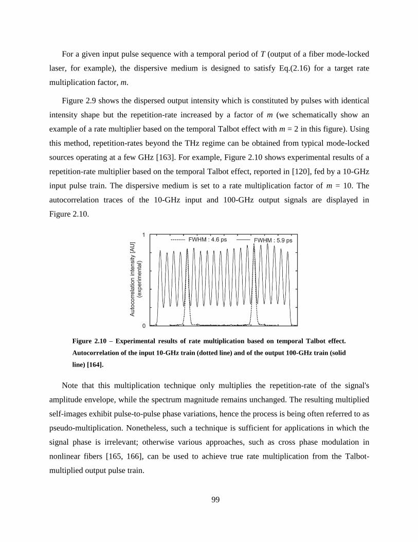
99
For a given input pulse sequence with a temporal period of T (output of a fiber mode-locked
laser, for example), the dispersive medium is designed to satisfy Eq.(2.16) for a target rate
multiplication factor, m.
Figure 2.9 shows the dispersed output intensity which is constituted by pulses with identical
intensity shape but the repetition-rate increased by a factor of m (we schematically show an
example of a rate multiplier based on the temporal Talbot effect with m = 2 in this figure). Using
this method, repetition-rates beyond the THz regime can be obtained from typical mode-locked
sources operating at a few GHz [163]. For example, Figure 2.10 shows experimental results of a
repetition-rate multiplier based on the temporal Talbot effect, reported in [120], fed by a 10-GHz
input pulse train. The dispersive medium is set to a rate multiplication factor of m = 10. The
autocorrelation traces of the 10-GHz input and 100-GHz output signals are displayed in
Figure 2.10.
Figure 2.10 – Experimental results of rate multiplication based on temporal Talbot effect.
Autocorrelation of the input 10-GHz train (dotted line) and of the output 100-GHz train (solid
line) [164].
Note that this multiplication technique only multiplies the repetition-rate of the signal's
amplitude envelope, while the spectrum magnitude remains unchanged. The resulting multiplied
self-images exhibit pulse-to-pulse phase variations, hence the process is being often referred to as
pseudo-multiplication. Nonetheless, such a technique is sufficient for applications in which the
signal phase is irrelevant; otherwise various approaches, such as cross phase modulation in
nonlinear fibers [165, 166], can be used to achieve true rate multiplication from the Talbot-
multiplied output pulse train.
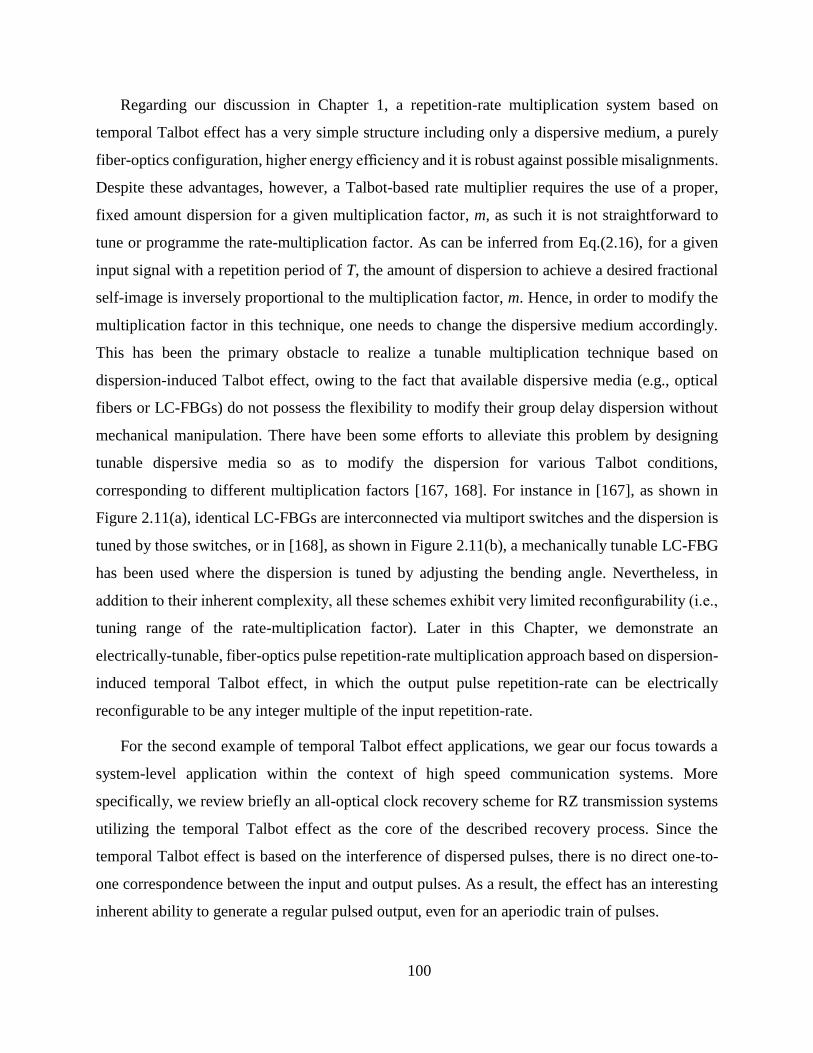
100
Regarding our discussion in Chapter 1, a repetition-rate multiplication system based on
temporal Talbot effect has a very simple structure including only a dispersive medium, a purely
fiber-optics configuration, higher energy efficiency and it is robust against possible misalignments.
Despite these advantages, however, a Talbot-based rate multiplier requires the use of a proper,
fixed amount dispersion for a given multiplication factor, m, as such it is not straightforward to
tune or programme the rate-multiplication factor. As can be inferred from Eq.(2.16), for a given
input signal with a repetition period of T, the amount of dispersion to achieve a desired fractional
self-image is inversely proportional to the multiplication factor, m. Hence, in order to modify the
multiplication factor in this technique, one needs to change the dispersive medium accordingly.
This has been the primary obstacle to realize a tunable multiplication technique based on
dispersion-induced Talbot effect, owing to the fact that available dispersive media (e.g., optical
fibers or LC-FBGs) do not possess the flexibility to modify their group delay dispersion without
mechanical manipulation. There have been some efforts to alleviate this problem by designing
tunable dispersive media so as to modify the dispersion for various Talbot conditions,
corresponding to different multiplication factors [167, 168]. For instance in [167], as shown in
Figure 2.11(a), identical LC-FBGs are interconnected via multiport switches and the dispersion is
tuned by those switches, or in [168], as shown in Figure 2.11(b), a mechanically tunable LC-FBG
has been used where the dispersion is tuned by adjusting the bending angle. Nevertheless, in
addition to their inherent complexity, all these schemes exhibit very limited reconfigurability (i.e.,
tuning range of the rate-multiplication factor). Later in this Chapter, we demonstrate an
electrically-tunable, fiber-optics pulse repetition-rate multiplication approach based on dispersion-
induced temporal Talbot effect, in which the output pulse repetition-rate can be electrically
reconfigurable to be any integer multiple of the input repetition-rate.
For the second example of temporal Talbot effect applications, we gear our focus towards a
system-level application within the context of high speed communication systems. More
specifically, we review briefly an all-optical clock recovery scheme for RZ transmission systems
utilizing the temporal Talbot effect as the core of the described recovery process. Since the
temporal Talbot effect is based on the interference of dispersed pulses, there is no direct one-to-
one correspondence between the input and output pulses. As a result, the effect has an interesting
inherent ability to generate a regular pulsed output, even for an aperiodic train of pulses.
101
Figure 2.11 – (a) Cascading LC-FBGs interconnected via multiport switches [167], (b)
Mechanically tunable LC-FBG [168].
This inherent property of the temporal Talbot effect has been applied toward a simple, passive,
and polarization-insensitive all-optical base-rate clock recovery scheme for RZ transmission
systems by Pudo et al [100, 99]. The term base-rate refers to the fact that, in the clock recovery
process, the repetition-rate of the output signal is equal to the input data signal’s bit rate. For this
purpose, the integer temporal Talbot effect (when m = 1) is used for designing the clock recovery
setup.
Figure 2.12 – Experimental setup used for proof-of-principle demonstration of all-optical clock
recovery using the temporal Talbot effect. The insets depict the autocorrelation and optical
spectrum of the input pulses [100, 99].
Figure 2.12 depicts the experimental setup of the clock recovery technique [100, 99]. The
output from a mode-locked fiber laser at 9.25 GHz is modulated by an electro-optic Mach–Zehnder
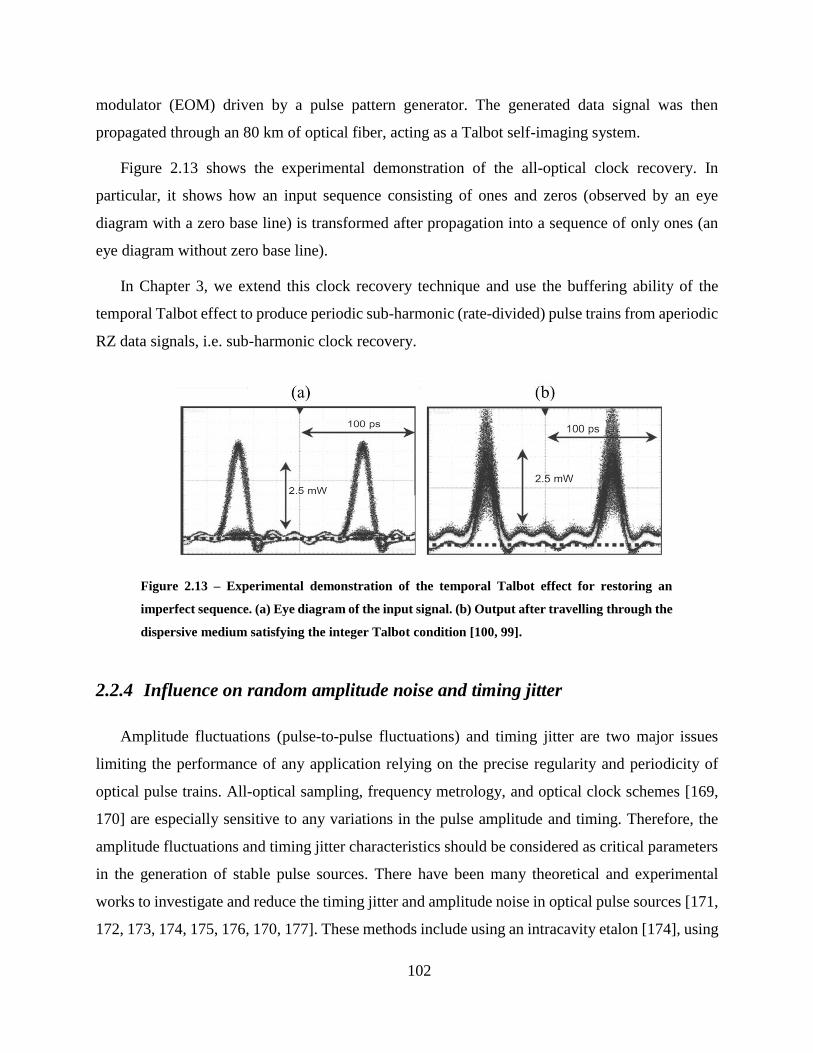
102
modulator (EOM) driven by a pulse pattern generator. The generated data signal was then
propagated through an 80 km of optical fiber, acting as a Talbot self-imaging system.
Figure 2.13 shows the experimental demonstration of the all-optical clock recovery. In
particular, it shows how an input sequence consisting of ones and zeros (observed by an eye
diagram with a zero base line) is transformed after propagation into a sequence of only ones (an
eye diagram without zero base line).
In Chapter 3, we extend this clock recovery technique and use the buffering ability of the
temporal Talbot effect to produce periodic sub-harmonic (rate-divided) pulse trains from aperiodic
RZ data signals, i.e. sub-harmonic clock recovery.
Figure 2.13 – Experimental demonstration of the temporal Talbot effect for restoring an
imperfect sequence. (a) Eye diagram of the input signal. (b) Output after travelling through the
dispersive medium satisfying the integer Talbot condition [100, 99].
2.2.4 Influence on random amplitude noise and timing jitter
Amplitude fluctuations (pulse-to-pulse fluctuations) and timing jitter are two major issues
limiting the performance of any application relying on the precise regularity and periodicity of
optical pulse trains. All-optical sampling, frequency metrology, and optical clock schemes [169,
170] are especially sensitive to any variations in the pulse amplitude and timing. Therefore, the
amplitude fluctuations and timing jitter characteristics should be considered as critical parameters
in the generation of stable pulse sources. There have been many theoretical and experimental
works to investigate and reduce the timing jitter and amplitude noise in optical pulse sources [171,
172, 173, 174, 175, 176, 170, 177]. These methods include using an intracavity etalon [174], using
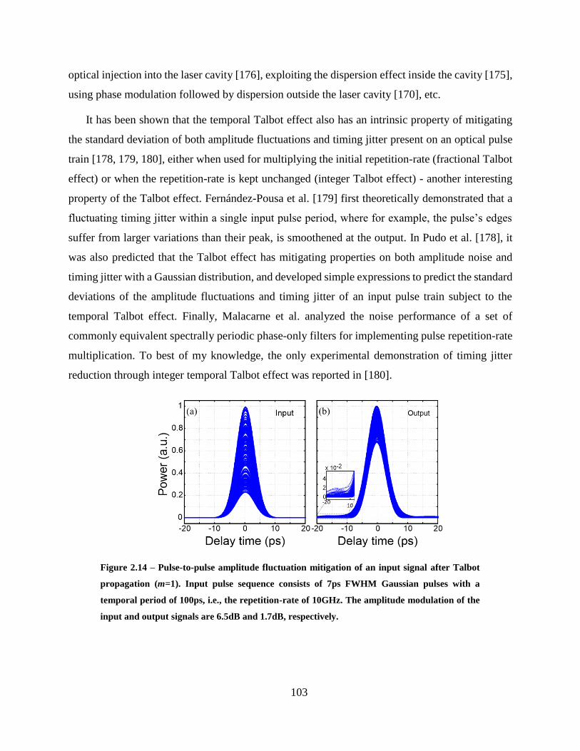
103
optical injection into the laser cavity [176], exploiting the dispersion effect inside the cavity [175],
using phase modulation followed by dispersion outside the laser cavity [170], etc.
It has been shown that the temporal Talbot effect also has an intrinsic property of mitigating
the standard deviation of both amplitude fluctuations and timing jitter present on an optical pulse
train [178, 179, 180], either when used for multiplying the initial repetition-rate (fractional Talbot
effect) or when the repetition-rate is kept unchanged (integer Talbot effect) - another interesting
property of the Talbot effect. Fernández-Pousa et al. [179] first theoretically demonstrated that a
fluctuating timing jitter within a single input pulse period, where for example, the pulse’s edges
suffer from larger variations than their peak, is smoothened at the output. In Pudo et al. [178], it
was also predicted that the Talbot effect has mitigating properties on both amplitude noise and
timing jitter with a Gaussian distribution, and developed simple expressions to predict the standard
deviations of the amplitude fluctuations and timing jitter of an input pulse train subject to the
temporal Talbot effect. Finally, Malacarne et al. analyzed the noise performance of a set of
commonly equivalent spectrally periodic phase-only filters for implementing pulse repetition-rate
multiplication. To best of my knowledge, the only experimental demonstration of timing jitter
reduction through integer temporal Talbot effect was reported in [180].
Figure 2.14 – Pulse-to-pulse amplitude fluctuation mitigation of an input signal after Talbot
propagation (m=1). Input pulse sequence consists of 7ps FWHM Gaussian pulses with a
temporal period of 100ps, i.e., the repetition-rate of 10GHz. The amplitude modulation of the
input and output signals are 6.5dB and 1.7dB, respectively.
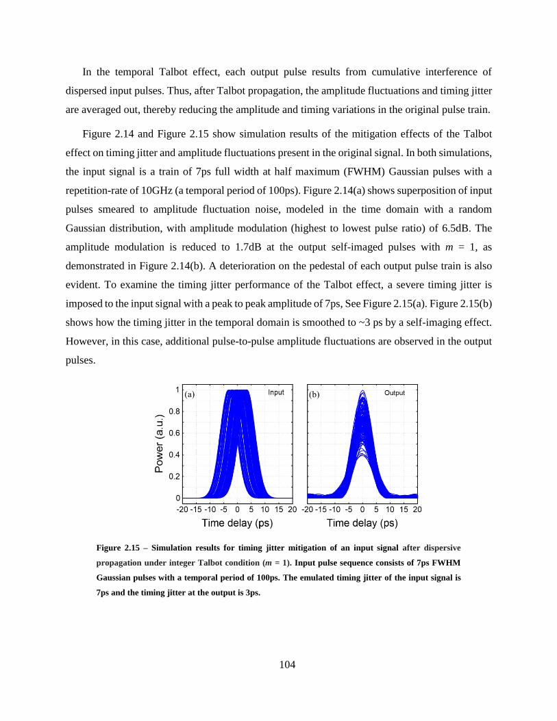
104
In the temporal Talbot effect, each output pulse results from cumulative interference of
dispersed input pulses. Thus, after Talbot propagation, the amplitude fluctuations and timing jitter
are averaged out, thereby reducing the amplitude and timing variations in the original pulse train.
Figure 2.14 and Figure 2.15 show simulation results of the mitigation effects of the Talbot
effect on timing jitter and amplitude fluctuations present in the original signal. In both simulations,
the input signal is a train of 7ps full width at half maximum (FWHM) Gaussian pulses with a
repetition-rate of 10GHz (a temporal period of 100ps). Figure 2.14(a) shows superposition of input
pulses smeared to amplitude fluctuation noise, modeled in the time domain with a random
Gaussian distribution, with amplitude modulation (highest to lowest pulse ratio) of 6.5dB. The
amplitude modulation is reduced to 1.7dB at the output self-imaged pulses with m = 1, as
demonstrated in Figure 2.14(b). A deterioration on the pedestal of each output pulse train is also
evident. To examine the timing jitter performance of the Talbot effect, a severe timing jitter is
imposed to the input signal with a peak to peak amplitude of 7ps, See Figure 2.15(a). Figure 2.15(b)
shows how the timing jitter in the temporal domain is smoothed to ~3 ps by a self-imaging effect.
However, in this case, additional pulse-to-pulse amplitude fluctuations are observed in the output
pulses.
Figure 2.15 – Simulation results for timing jitter mitigation of an input signal after dispersive
propagation under integer Talbot condition (m = 1). Input pulse sequence consists of 7ps FWHM
Gaussian pulses with a temporal period of 100ps. The emulated timing jitter of the input signal is
7ps and the timing jitter at the output is 3ps.
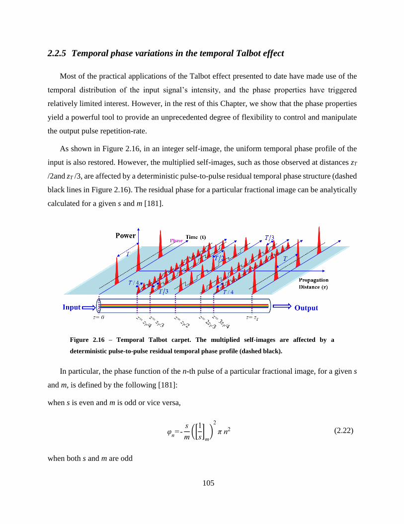
105
2.2.5 Temporal phase variations in the temporal Talbot effect
Most of the practical applications of the Talbot effect presented to date have made use of the
temporal distribution of the input signal’s intensity, and the phase properties have triggered
relatively limited interest. However, in the rest of this Chapter, we show that the phase properties
yield a powerful tool to provide an unprecedented degree of flexibility to control and manipulate
the output pulse repetition-rate.
As shown in Figure 2.16, in an integer self-image, the uniform temporal phase profile of the
input is also restored. However, the multiplied self-images, such as those observed at distances zT
/2and zT /3, are affected by a deterministic pulse-to-pulse residual temporal phase structure (dashed
black lines in Figure 2.16). The residual phase for a particular fractional image can be analytically
calculated for a given s and m [181].
Figure 2.16 – Temporal Talbot carpet. The multiplied self-images are affected by a
deterministic pulse-to-pulse residual temporal phase profile (dashed black).
In particular, the phase function of the n-th pulse of a particular fractional image, for a given s
and m, is defined by the following [181]:
when s is even and m is odd or vice versa,
φn=-
s
m([
1
s]
m
)2
π n2 (2.22)
when both s and m are odd
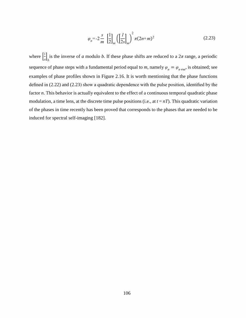
106
φn=-2
s
m [
1
2]
m
([1
2s]
m
)2
π(2n+m)2 (2.23)
where [1
a]
bis the inverse of a modulo b. If these phase shifts are reduced to a 2π range, a periodic
sequence of phase steps with a fundamental period equal to m, namely φn
= φn+m
, is obtained; see
examples of phase profiles shown in Figure 2.16. It is worth mentioning that the phase functions
defined in (2.22) and (2.23) show a quadratic dependence with the pulse position, identified by the
factor n. This behavior is actually equivalent to the effect of a continuous temporal quadratic phase
modulation, a time lens, at the discrete time pulse positions (i.e., at t = nT). This quadratic variation
of the phases in time recently has been proved that corresponds to the phases that are needed to be
induced for spectral self-imaging [182].


122
2.4 Lossless fractional repetition-rate multiplication of optical pulse
trains19
2.4.1 Abstract
We propose and experimentally demonstrate repetition-rate multiplication of picosecond
optical pulse trains by a fractional factor based on temporal self-imaging, involving temporal phase
modulation and first-order dispersion. Multiplication factors of 1.25, 1.33, 1.5, 1.6, 1.75, 2.25, 2.33
and 2.5 are achieved with high fidelity from a mode-locked laser with an input repetition-rate
between 10 and 20 GHz.
2.4.2 Introduction
The generation of high repetition-rate optical pulse trains is of great interest for high bit-rate
optical communications, optical computing systems, and both optical and microwave waveform
generation [190, 191]. One attractive method for generating high repetition-rate optical pulse trains
is to multiply the repetition-rate of a lower repetition-rate pulse train in the optical domain as
opposed to electronically, overcoming bandwidth limitations of high speed electronics [121, 123,
192, 124, 120, 41]. Among previously demonstrated pulse repetition-rate multiplication (PRRM)
techniques, the approach based on the temporal self-imaging (TSI) or Talbot effect [120, 41] has
attracted a great deal of attention over the years. This approach provides the desired multiplied
repetition-rate copy of an incoming optical pulse train without distorting the individual pulse
features (shape and time width) simply by applying a proper dispersion-induced spectral phase
profile on the original pulse train. Additionally, this method provides increased energy efficiency
since fundamentally no energy is lost in the phase-filtering process. However, despite the
advantages of TSI-based PRRM, the method is limited to output repetition-rates that are integer
multiples of the initial pulse repetition-rate. This same restriction applies to all PRRM methods
reported to date [121, 123, 192, 124, 120, 41].
19 R. Maram, J. Van Howe, M. Li, and J. Azaña, “Lossless fractional pulse repetition-rate multiplication of optical
pulse trains,” Optics Letters, vol. 40, no. 3, pp. 375-378, (2015).
123
In this Letter, we propose and experimentally demonstrate, for the first time to our knowledge,
“fractional” pulse repetition-rate multiplication (F-PRRM) based on TSI. Using our newly
proposed method, the output pulse train repetition-rate can ideally be designed to be any fractional
multiple of the input repetition-rate. The proposed concept shares the above-mentioned advantages
of TSI-based PRRM yet it provides an additional, unprecedented degree of flexibility to set the
output pulse repetition-rate.
2.4.3 The operation principle
The principle of our proposed fractional pulse repetition-rate multiplication concept is
illustrated in Figure 2.23. Figure 2.23(a) represents the well-known standard temporal self-imaging
(Talbot) effect in which a flat-phase repetitive input waveform (signal at z = 0) is self-imaged after
dispersive propagation through an integer number of Talbot distances, zT. In this representation,
first-order dispersive propagation, involving a linear group delay profile, is assumed. Moreover,
in addition to the mentioned ‘integer’ self-images, rate-multiplied self-images of the original input
waveform train are obtained at fractional values of the fundamental Talbot distance, zT, as defined
by the “Talbot Carpet” [41]; see examples in Figure 2.23(a) at the fractional Talbot distances zT
/2, 2zT /3 and 3zT /4. Dispersive propagation speeds up and slows down the different frequency-
components ‘colors’, originally in-phase that make up the waveform train, redistributing the
original signal energy into the mentioned different temporal intensity patterns. An integer self-
image exhibits the same repetition-rate as the input, whereas in the multiplied self-images, the
repetition-rate is increased by an integer factor. In particular, the repetition-rate multiplication
factors for the multiplied self-images shown in Figure 2.23(a) at zT /2, 2zT /3 and 3zT /4 are integer
numbers of 2, 3 and 4, respectively. We also recall that the term self-image refers to the fact that
the temporal shape of each individual waveform in the Talbot patterns is an exact, undistorted copy
of the input (under ideal conditions that the input is completely periodic and that the output is
generated by purely linear group delay). Additionally, in an integer self-image, the uniform
temporal phase profile of the input is also restored. However, in the multiplied self-images, such
as those observed at distances zT /2, 2zT /3 and 3zT /4, there exists a waveform-to-waveform residual
temporal phase structure (dashed black lines in the figure). This residual temporal phase represents
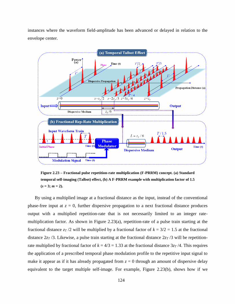
124
instances where the waveform field-amplitude has been advanced or delayed in relation to the
envelope center.
Figure 2.23 – Fractional pulse repetition-rate multiplication (F-PRRM) concept. (a) Standard
temporal self-imaging (Talbot) effect, (b) A F-PRRM example with multiplication factor of 1.5
(s = 3; m = 2).
By using a multiplied image at a fractional distance as the input, instead of the conventional
phase-free input at z = 0, further dispersive propagation to a next fractional distance produces
output with a multiplied repetition-rate that is not necessarily limited to an integer rate-
multiplication factor. As shown in Figure 2.23(a), repetition-rate of a pulse train starting at the
fractional distance zT /2 will be multiplied by a fractional factor of k = 3/2 = 1.5 at the fractional
distance 2zT /3. Likewise, a pulse train starting at the fractional distance 2zT /3 will be repetition-
rate multiplied by fractional factor of k = 4/3 = 1.33 at the fractional distance 3zT /4. This requires
the application of a prescribed temporal phase modulation profile to the repetitive input signal to
make it appear as if it has already propagated from z = 0 through an amount of dispersive delay
equivalent to the target multiple self-image. For example, Figure 2.23(b), shows how if we
125
condition a typical flat-phase repetitive input pulses to look like the waveform train at zT /2 by
proper temporal phase modulation (dashed black line), subsequent propagation through zT /6 more
of dispersive delay will give the output shown at 2zT /3, one and a half the input repetition-rate (k
= 1.5). Notice that the described processes involve only a suitable manipulation of the input signal
temporal and spectral phase profiles, not magnitude, ensuring that the original signal energy is
ideally preserved. According to the Talbot carpet, any desired fractional repetition-rate
multiplication factor can be obtained, as long as the output period is sufficiently long so that
individual pulse waveforms do not overlap along the time domain.
Notice that one can use the F-PRRM technique to also obtain integer factors, providing added
versatility in the PRRM process design. As an example, the repetition-rate of a pulse train starting
at the fractional distance zT /2 will be multiplied by an integer factor of 2 at the fractional distance
3zT /4. Moreover, the target PRRM factor can be smaller than 1, actually implementing a repetition-
rate division process [188].
2.4.4 System design
The required temporal phase modulation profile can be deduced from the self-imaging theory
[41]. Assume that we target increasing the original repetition-rate (F = 1/T ) by a desired fractional
factor k = (s/m) with s = 1, 2, 3, … and m = 2, 3, 4, …, where s and m are co-prime integers.
Accordingly, the temporal period of the output pulse train will be TOut = T / k = (m/s)T, (FOut =
1/TOut being the output repetition-rate). In this case, a temporal phase of
φn=
m-1
mπn2 (2.36)
must be applied on the n-th incoming temporal pulse (n = 0,1,2,…, m-1). The temporal phase φn
can be assumed to be applied on time slots equal to the pulse repetition-rate. In practice, however,
it is sufficient to apply the same phase over the pulse duration. If these phase shifts are reduced to
a 2π range, a periodic sequence of phase steps with a fundamental period equal to m, namely ϕn+m,
is obtained. These phase shifts have been shown to induce a spectral self-imaging effect on the
modulated pulse train [188, 75]. In particular, the temporal phase modulation process reduces the
comb frequency spacing of the input signal by m times [75]. As mentioned above, prescription of
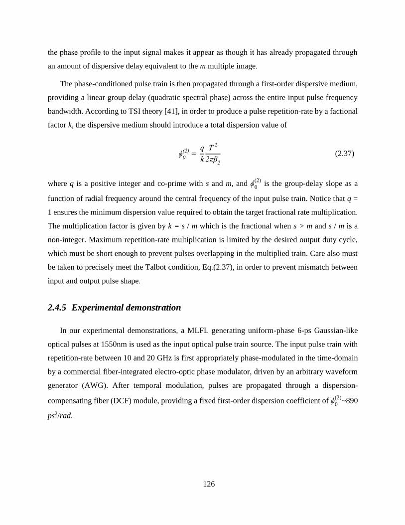
126
the phase profile to the input signal makes it appear as though it has already propagated through
an amount of dispersive delay equivalent to the m multiple image.
The phase-conditioned pulse train is then propagated through a first-order dispersive medium,
providing a linear group delay (quadratic spectral phase) across the entire input pulse frequency
bandwidth. According to TSI theory [41], in order to produce a pulse repetition-rate by a factional
factor k, the dispersive medium should introduce a total dispersion value of
ϕ0
(2) =
q
k
T 2
2πβ2
(2.37)
where q is a positive integer and co-prime with s and m, and ϕ0
(2) is the group-delay slope as a
function of radial frequency around the central frequency of the input pulse train. Notice that q =
1 ensures the minimum dispersion value required to obtain the target fractional rate multiplication.
The multiplication factor is given by k = s / m which is the fractional when s > m and s / m is a
non-integer. Maximum repetition-rate multiplication is limited by the desired output duty cycle,
which must be short enough to prevent pulses overlapping in the multiplied train. Care also must
be taken to precisely meet the Talbot condition, Eq.(2.37), in order to prevent mismatch between
input and output pulse shape.
2.4.5 Experimental demonstration
In our experimental demonstrations, a MLFL generating uniform-phase 6-ps Gaussian-like
optical pulses at 1550nm is used as the input optical pulse train source. The input pulse train with
repetition-rate between 10 and 20 GHz is first appropriately phase-modulated in the time-domain
by a commercial fiber-integrated electro-optic phase modulator, driven by an arbitrary waveform
generator (AWG). After temporal modulation, pulses are propagated through a dispersion-
compensating fiber (DCF) module, providing a fixed first-order dispersion coefficient of ϕ0
(2)~890
ps2/rad.
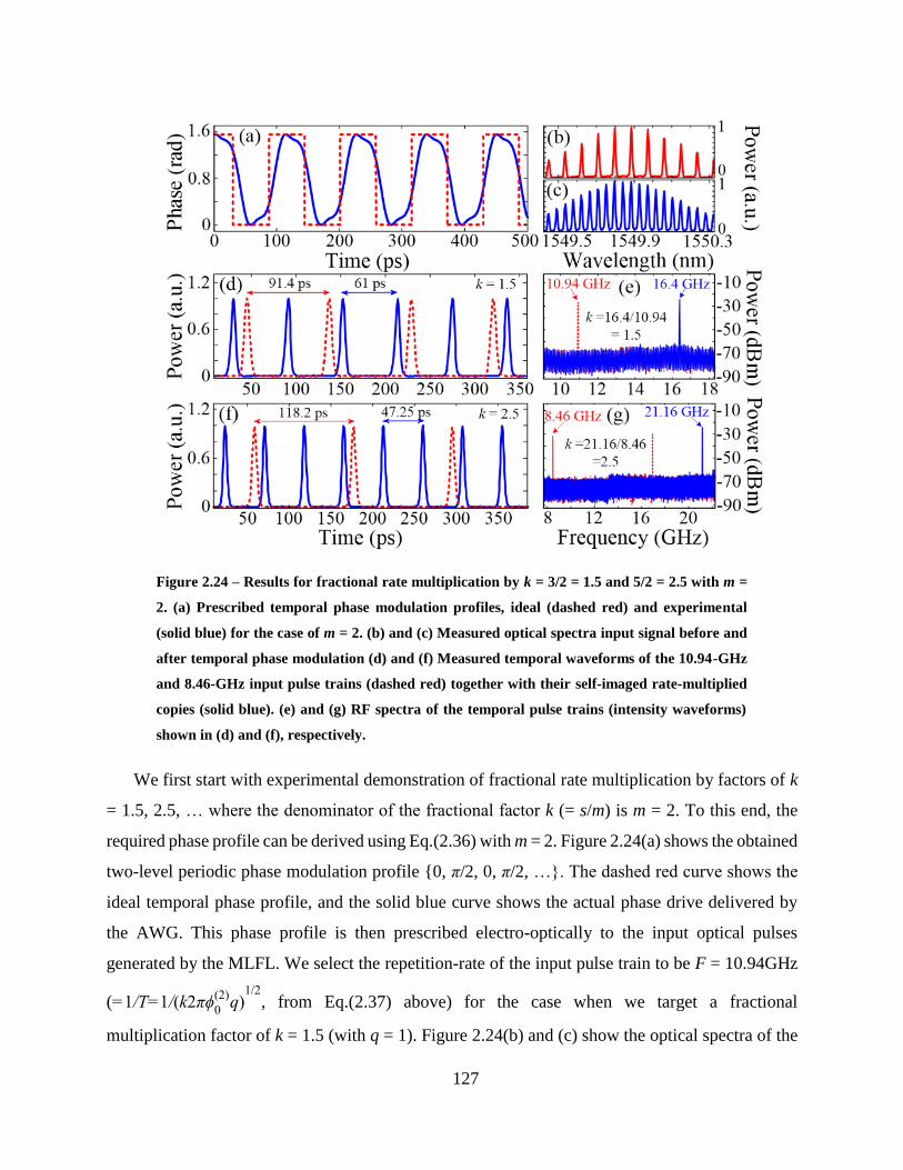
127
Figure 2.24 – Results for fractional rate multiplication by k = 3/2 = 1.5 and 5/2 = 2.5 with m =
2. (a) Prescribed temporal phase modulation profiles, ideal (dashed red) and experimental
(solid blue) for the case of m = 2. (b) and (c) Measured optical spectra input signal before and
after temporal phase modulation (d) and (f) Measured temporal waveforms of the 10.94-GHz
and 8.46-GHz input pulse trains (dashed red) together with their self-imaged rate-multiplied
copies (solid blue). (e) and (g) RF spectra of the temporal pulse trains (intensity waveforms)
shown in (d) and (f), respectively.
We first start with experimental demonstration of fractional rate multiplication by factors of k
= 1.5, 2.5, … where the denominator of the fractional factor k (= s/m) is m = 2. To this end, the
required phase profile can be derived using Eq.(2.36) with m = 2. Figure 2.24(a) shows the obtained
two-level periodic phase modulation profile {0, π/2, 0, π/2, …}. The dashed red curve shows the
ideal temporal phase profile, and the solid blue curve shows the actual phase drive delivered by
the AWG. This phase profile is then prescribed electro-optically to the input optical pulses
generated by the MLFL. We select the repetition-rate of the input pulse train to be F = 10.94GHz
(=1/T=1/(k2πϕ0
(2)q)
1/2, from Eq.(2.37) above) for the case when we target a fractional
multiplication factor of k = 1.5 (with q = 1). Figure 2.24(b) and (c) show the optical spectra of the
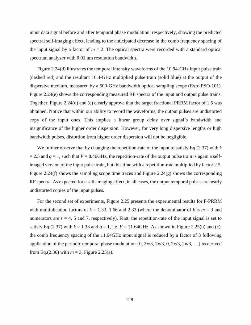
128
input data signal before and after temporal phase modulation, respectively, showing the predicted
spectral self-imaging effect, leading to the anticipated decrease in the comb frequency spacing of
the input signal by a factor of m = 2. The optical spectra were recorded with a standard optical
spectrum analyzer with 0.01 nm resolution bandwidth.
Figure 2.24(d) illustrates the temporal intensity waveforms of the 10.94-GHz input pulse train
(dashed red) and the resultant 16.4-GHz multiplied pulse train (solid blue) at the output of the
dispersive medium, measured by a 500-GHz bandwidth optical sampling scope (Exfo PSO-101).
Figure 2.24(e) shows the corresponding measured RF spectra of the input and output pulse trains.
Together, Figure 2.24(d) and (e) clearly approve that the target fractional PRRM factor of 1.5 was
obtained. Notice that within our ability to record the waveforms, the output pulses are undistorted
copy of the input ones. This implies a linear group delay over signal’s bandwidth and
insignificance of the higher order dispersion. However, for very long dispersive lengths or high
bandwidth pulses, distortion from higher order dispersion will not be negligible.
We further observe that by changing the repetition-rate of the input to satisfy Eq.(2.37) with k
= 2.5 and q = 1, such that F = 8.46GHz, the repetition-rate of the output pulse train is again a self-
imaged version of the input pulse train, but this time with a repetition-rate multiplied by factor 2.5.
Figure 2.24(f) shows the sampling scope time traces and Figure 2.24(g) shows the corresponding
RF spectra. As expected for a self-imaging effect, in all cases, the output temporal pulses are nearly
undistorted copies of the input pulses.
For the second set of experiments, Figure 2.25 presents the experimental results for F-PRRM
with multiplication factors of k = 1.33, 1.66 and 2.33 (where the denominator of k is m = 3 and
numerators are s = 4, 5 and 7, respectively). First, the repetition-rate of the input signal is set to
satisfy Eq.(2.37) with k = 1.33 and q = 1, i.e. F = 11.64GHz. As shown in Figure 2.25(b) and (c),
the comb frequency spacing of the 11.64GHz input signal is reduced by a factor of 3 following
application of the periodic temporal phase modulation {0, 2π/3, 2π/3, 0, 2π/3, 2π/3, …} as derived
from Eq.(2.36) with m = 3, Figure 2.25(a).
129
Figure 2.25 – Experimental results for fractional rate multiplication by k = 1.33, 2.33 and 1.66
with m = 3, with the same captions as for the Fig. 2.
The slight reduction in the fidelity of the Gaussian spectral envelope is due to the time-
resolution limitations of the AWG, which fails to reproduce the ideal temporal phase drive.
Because a constant phase is only required over the pulse width, it may be possible to synthesize
smoother phase profiles to relax the bandwidth requirement of the AWG. Figure 2.25(d) shows
that the output signal (solid blue) reproduces the input signal (dashed red) but with 1.33 times the
repetition-rate, confirmed further by the corresponding RF spectra in Figure 2.25(e). Next, we
consider input pulse trains with repetition-rates of F = 8.77GHz and 14.73GHz (calculated to
satisfy Eq.(2.37) with k = 2.33 (q = 1) and 1.66 (q = 2), respectively). At the output of the setup
we obtain the predicted 20.46-GHz and 24.52-GHz optical pulse trains, achieving the target
repetition-rate multiplication by 2.33 and 1.66, respectively, as illustrated in Figure 2.25(f),(h) and
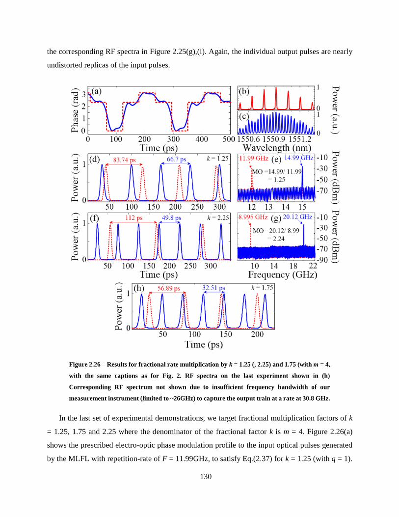
130
the corresponding RF spectra in Figure 2.25(g),(i). Again, the individual output pulses are nearly
undistorted replicas of the input pulses.
Figure 2.26 – Results for fractional rate multiplication by k = 1.25 (, 2.25) and 1.75 (with m = 4,
with the same captions as for Fig. 2. RF spectra on the last experiment shown in (h)
Corresponding RF spectrum not shown due to insufficient frequency bandwidth of our
measurement instrument (limited to ~26GHz) to capture the output train at a rate at 30.8 GHz.
In the last set of experimental demonstrations, we target fractional multiplication factors of k
= 1.25, 1.75 and 2.25 where the denominator of the fractional factor k is m = 4. Figure 2.26(a)
shows the prescribed electro-optic phase modulation profile to the input optical pulses generated
by the MLFL with repetition-rate of F = 11.99GHz, to satisfy Eq.(2.37) for k = 1.25 (with q = 1).
131
The periodic temporal phase profile is {0, 3π/4, π, 3 π/4, 0, 3 π/4, π, …} when m = 4 in Eq.(2.36),
Figure 2.26(a). Likewise our previous demonstrations, the comb frequency spacing of the input
signal is reduced after phase modulation, in this case, by a factor of m = 4, as depicted in
Figure 2.26(b) and (c). Figure 2.26(d) and (e) show experimental temporal scope traces and RF
spectra for both the input (F = 11.99GHz) and 1.25 times repetition-rate output (FOut = 14.99GHz).
Finally, by adjusting the repetition-rate of the input pulse train to 8.99GHz (with q = 1) and
17.6GHz (with q = 3), we would have the 2.25 and 1.75 multiplied pulse trains with 20.12 and
30.8GHz repetition-rates, respectively, as shown in Figure 2.26(f)-(h).
2.4.6 Conclusion
In summary, we have proposed and experimentally demonstrated a simple and practical
lossless method for undistorted optical PRRM by any desired fractional factor. The demonstrated
technique offers an unprecedented degree of flexibility compared with previously reported PRRM
approaches, which are generally limited to integer repetition-rate multiplication factors. The
method exploits temporal self-imaging effects and it involves temporal phase modulation
combined with dispersive (phase-only spectral) filtering, fundamentally preserving the input pulse
train energy.
132
2.5 Noiseless Intensity Amplification of Repetitive Signals by
Coherent Addition using the Temporal Talbot Effect20
2.5.1 Abstract
Amplification of signal intensity is essential for initiating physical processes, diagnostics,
sensing, communications, and measurement. During traditional amplification, the signal is
amplified by multiplying the signal carriers through an active gain process, requiring the use of an
external power source. Additionally, the signal is degraded by noise and distortions that typically
accompany active gain processes. We show noiseless intensity amplification of repetitive optical
pulse waveforms with gain from 2 to ~20 without using active gain. The proposed method uses a
dispersion-induced temporal self-imaging (Talbot) effect to re-distribute and coherently
accumulate energy of the original repetitive waveforms into fewer replica waveforms. In addition,
we show how our passive amplifier performs a real-time average of the wave-train to reduce its
original noise fluctuation, as well as enhances the extinction ratio of pulses to stand above the
noise floor. Our technique is applicable to repetitive waveforms in any spectral region or wave
system.
2.5.2 Introduction
Waveform amplification refers to a process by which the amplitude of the waveform is
increased without affecting its other signal features, particularly temporal shape. Intensity
amplification of waveforms is necessary for increasing the peak power of signals for initiating
physical processes, extracting information from the natural world, and communications. Almost
every information-bearing electronic signal used for diagnostics, sensing, or fundamental
measurement requires amplification between the source and the detector. Optical pulses amplified
to high-intensities are necessary for nonlinear microscopy [193], materials processing [194], and
relativistic optical processes [195] such as coherent x-ray generation, laser fusion, and particle
20 R. Maram, J. Van Howe, M. Li and J. Azaña, “Noiseless intensity amplification of repetitive signals by coherent
addition using the temporal Talbot effect” Nature Communications, vol. 5, 4827, (doi: 10.1038/ncomms6163), (2014).
133
acceleration. Additionally, optical amplification of signal intensity is critical for communications
and becoming increasingly important for current work in optical computing and optical
information processing [196, 197, 198]. During active amplification, the signal is amplified
directly by multiplying the signal carriers through an active gain process using an external power
source [199, 200, 201, 202, 203, 204, 205, 206]. Whereas active gain mechanisms are widely
available for electrical and optical signals, suitable active gain processes for direct waveform
amplification are limited over large regions of the electromagnetic spectrum and for other wave
systems, such as mechanical, acoustic, and quantum probability waves.
Furthermore, for applications involving high-peak power pulse generation [193, 194, 195],
traditional active amplification is extremely inefficient. In order to generate high-peak power
optical pulses, many pulses in a wave-train are intentionally thrown away, “pulse-picking,” either
prior to amplification [207] or during the amplification process (regenerative amplification) [208],
in order to concentrate energy from the external source in fewer remaining output pulses. In such
processes, typically more than 99% of the signal energy is thrown away prior to boosting. While
absolute power consumption in high-peak power amplification is dominated by the pumps on the
high-power boosting amplifier after pulse-picking, carelessly throwing away 99% of the signal
prior to active-amplification significantly reduces the signal-to-noise and is enough of a power hit
to be a problem for high-peak power applications [209].
Finally, in applications where active amplification is employed, the active-gain process
typically contributes amplitude and phase noise, such as amplified spontaneous emission (ASE)
noise or timing jitter, and other signal distortions induced by limited gain frequency bandwidth.
Because an active-gain process inherently amplifies input noise and also injects its own noise onto
a signal, the output signal-to-noise ratio (SNR) degrades. This degradation is encapsulated by a
common figure-of-merit of any active amplifier- the noise figure [210]. The noise figure of an
active amplifier is the ratio of the SNR of the input signal to the SNR of the output signal. Though
phase-sensitive amplifiers have been shown capable of realizing low-noise amplification (with
noise figures as low as 1 dB [206]), the amplification of weak signals by conventional amplifiers
typically renders the signal totally undetectable due to the amplification and injection of noise.
Coherent addition of repetitive optical pulses in a wave-train has been used in the past with the
aim of overcoming the drawbacks described above. However, controlled coherent addition of
134
many identical waveforms is an extremely challenging process. Previous methods are based on
precisely timing and storing pulses in a high-finesse cavity [209, 211]. As such, these methods
require ultra-precise active phase control of the input signal envelope and carrier, i.e., carrier-
envelope phase stabilization, in order to stabilize the input waveforms to cavity such that each
pulse will add constructively. Otherwise, small phase misalignment in each pulse tends towards
destructive interference. Though impressive results have been reported, these conditions are much
too restrictive to be applied beyond a controlled lab environment.
Using optical pulses, we demonstrate a noiseless waveform amplification method for repetitive
signals with experimental intensity gain from 2 to ~20, without using an active gain process,
through coherent addition. Our new concept of passive amplification exploits the intrinsic
coherence revival times of periodic waveform trains provided by passive dispersive broadening,
known as temporal “self-imaging” or the temporal Talbot effect [41] (illustrated in Fig. 1, top). In
particular, passive amplification is achieved by effectively re-distributing and coherently adding
the overall input energy of a repetitive waveform signal into fewer waveforms, resulting in each
output individual waveform to be an amplified copy of the input. Essentially, we implement a
“lossless” pulse picking process by using a suitable combination of phase-only temporal and
spectral modulation operations, in order to preserve the overall input signal energy. This can be
interpreted as coherently adding a desired number of identical copies on top of one another to
produce the desired amplified output. However, in sharp contrast to previous pulse coherent-
addition methods, our technique implements a similar process without using a cavity and therefore
without the associated stringent timing and stabilization conditions. The only condition on the
input waveform is that it is repetitive and maintains coherence over the output repetition-rate.
Because our passive amplification technique for repetitive signals is based upon the fundamental
process of linear superposition of waves, it can be applied to any wave system, introducing a
method for multiplying signal intensity in systems where active gain processes for waveform
amplification are limited or do not exist.
Last but not least, we report numerical and experimental results to demonstrate that during
passive intensity amplification, the SNR does not degrade. In fact, the proposed Talbot-based
amplification technique improves random (white) intensity noise, ASE-like fluctuations, present
on the input temporal signal, similarly to a real-time averaging process, as well as enhances the
135
extinction ratio compared to the input waveform train in the time-domain. In particular, consistent
with simulation, we show experimentally that Talbot-based passive amplification increases the
extinction ratio by approximately the passive gain factor, m, as well as performs a real-time
average of the waveform train by about m averages. These noise-mitigating effects allow us to
show in a side-by-side comparison in one of our experiments how Talbot-amplification can extract
a weak noisy signal nearly buried beneath a noisy background whereas a typical active amplifier
buries the signal further beneath the noise. We also anticipate that Talbot amplification improves
pulse-to-pulse fluctuation [212] and timing-jitter present on the input signal as the passive gain
factor increases. This is consistent with previous experiments which show improvement in timing-
jitter and pulse-to-pulse fluctuation for simple self-imaging (passive gain factor of 1m ) [178,
179]. Noise mitigation using Talbot passive amplification therefore shows promise for further
signal regeneration than the results presented in this report.
2.5.3 Concept and operation principle
Figure 2.27 illustrates the concept of our passive amplification technique. We effectively
exploit an “inverse temporal Talbot effect” in which the final amplified temporal image is
recovered from a previous multiplied self-image. As shown in Figure 2.27, top, in the standard
temporal Talbot effect, a flat-phase repetitive input waveform (signal at 0z ) is self-imaged,
after dispersive propagation through a distance zT (integer Talbot distances). There also exists an
infinite amount of fractional distances, given by the “Talbot Carpet” (a map of all possible
coherence revivals resembling a Persian rug in intricate but repeating patterns) [41] that give
multiplied self-images; see examples at the fractional Talbot distances zT /2 and 2zT /3, Figure 2.27,
top. Dispersive propagation speeds up and slows down the different frequency-components
‘colors’, originally in-phase that make up the waveform train, redistributing the original signal
energy into the mentioned different temporal intensity patterns. An integer self-image exhibits the
same repetition-rate and individual waveform intensity as the input, whereas in the multiplied self-
images, the repetition-rate is increased, and the individual waveform intensity is correspondingly
decreased by an integer factor. The repetition-rate-multiplication (intensity-division) factors for
the multiplied self-images shown in Figure 2.27 at zT /2 and 2zT /3 are 2 and 3, respectively. In an
integer self-image, the uniform temporal phase profile of the input is restored. However, in the
136
multiplied self-images, such as those observed at distances zT /2 and 2zT /3, there exists a
waveform-to-waveform residual temporal phase structure (dashed black). This residual temporal
phase represents instances where the waveform field-amplitude has been advanced or delayed in
relation to the envelope center.
By using a multiplied image at a fractional distance as the input instead of the conventional
phase-free input at 0z , further dispersive propagation to the distance zT produces an output with
an amplified intensity. As shown by Figure 2.27 top, a waveform starting at the fractional distance
zT /2 will be amplified in intensity by a factor of 2m at the output zT. Likewise, a waveform
starting at the fractional distance 2zT /3 will be amplified by a factor of 3m . This requires the
application of a prescribed temporal phase modulation profile to an input signal to make it appear
as though it has already propagated from 0z through an amount of dispersive delay equivalent
to the target multiple image. For example, Figure 2.27, bottom, shows how if we condition a typical
flat-phase input to look like the waveform train at 2zT /3 by proper temporal phase modulation
(dashed black line), subsequent propagation through zT /3 more of dispersive delay will give the
output shown at zT, one-third the repetition-rate and three times the intensity. Notice that the
described processes involve only a suitable manipulation of the input signal temporal and spectral
phase profiles, not magnitude, ensuring that the signal energy is ideally preserved. The full Talbot
carpet provides an infinite amount of fractional self-image locations and corresponding phase
profiles, so that any desired repetition-rate division and corresponding amplification factor can be
obtained, limited only practically by the control of temporal phase modulation and spectral phase
filtering from dispersive propagation.
To passively amplify any arbitrary repetitive input signal by m times ( 2,3,4,...m ), a
temporal phase of
φn=
m-1
mπn2 (2.38)
(where 1s m ) is applied on the n -th temporal pulse ( 0,1,2,...n ) of the input periodic signal.
This is followed by propagation through a first-order dispersive medium, ideally providing a linear
group-delay variation as a function of frequency over the signal spectral bandwidth. The dispersive
medium should introduce a total dispersion value:
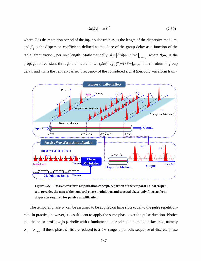
137
2π|β2| = mT 2 (2.39)
where T is the repetition period of the input pulse train, zA is the length of the dispersive medium,
and β2 is the dispersion coefficient, defined as the slope of the group delay as a function of the
radial frequency , per unit length. Mathematically, β2=[∂2
β(ω) / ∂ω2]ω=ω0
, where β(ω) is the
propagation constant through the medium, i.e. τg(ω)=zA[∂β(ω) / ∂ω]ω=ω0 is the medium’s group
delay, and 0 is the central (carrier) frequency of the considered signal (periodic waveform train).
Figure 2.27 – Passive waveform amplification concept. A portion of the temporal Talbot carpet,
top, provides the map of the temporal phase modulation and spectral phase-only filtering from
dispersion required for passive amplification.
The temporal phase φn can be assumed to be applied on time slots equal to the pulse repetition-
rate. In practice, however, it is sufficient to apply the same phase over the pulse duration. Notice
that the phase profile φnis periodic with a fundamental period equal to the gain-factor m , namely
φn
= φn+m
. If these phase shifts are reduced to a 2 range, a periodic sequence of discrete phase
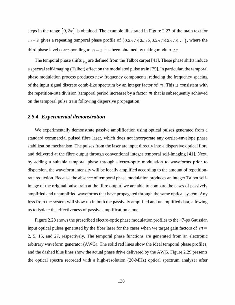
138
steps in the range 0, 2 is obtained. The example illustrated in Figure 2.27 of the main text for
3m gives a repeating temporal phase profile of 0, 2 / 3, 2 / 3, 0, 2 / 3,2 / 3, , where the
third phase level corresponding to 2n has been obtained by taking modulo 2 .
The temporal phase shifts φn are defined from the Talbot carpet [41]. These phase shifts induce
a spectral self-imaging (Talbot) effect on the modulated pulse train [75]. In particular, the temporal
phase modulation process produces new frequency components, reducing the frequency spacing
of the input signal discrete comb-like spectrum by an integer factor of m . This is consistent with
the repetition-rate division (temporal period increase) by a factor m that is subsequently achieved
on the temporal pulse train following dispersive propagation.
2.5.4 Experimental demonstration
We experimentally demonstrate passive amplification using optical pulses generated from a
standard commercial pulsed fibre laser, which does not incorporate any carrier-envelope phase
stabilization mechanism. The pulses from the laser are input directly into a dispersive optical fibre
and delivered at the fibre output through conventional integer temporal self-imaging [41]. Next,
by adding a suitable temporal phase through electro-optic modulation to waveforms prior to
dispersion, the waveform intensity will be locally amplified according to the amount of repetition-
rate reduction. Because the absence of temporal phase modulation produces an integer Talbot self-
image of the original pulse train at the fibre output, we are able to compare the cases of passively
amplified and unamplified waveforms that have propagated through the same optical system. Any
loss from the system will show up in both the passively amplified and unamplified data, allowing
us to isolate the effectiveness of passive amplification alone.
Figure 2.28 shows the prescribed electro-optic phase modulation profiles to the ~7-ps Gaussian
input optical pulses generated by the fiber laser for the cases when we target gain factors of m
2, 5, 15, and 27, respectively. The temporal phase functions are generated from an electronic
arbitrary waveform generator (AWG). The solid red lines show the ideal temporal phase profiles,
and the dashed blue lines show the actual phase drive delivered by the AWG. Figure 2.29 presents
the optical spectra recorded with a high-resolution (20-MHz) optical spectrum analyzer after
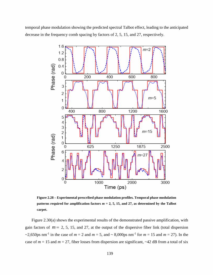
139
temporal phase modulation showing the predicted spectral Talbot effect, leading to the anticipated
decrease in the frequency comb spacing by factors of 2, 5, 15, and 27, respectively.
Figure 2.28 – Experimental prescribed phase modulation profiles. Temporal phase modulation
patterns required for amplification factors m = 2, 5, 15, and 27, as determined by the Talbot
carpet.
Figure 2.30(a) shows the experimental results of the demonstrated passive amplification, with
gain factors of m 2, 5, 15, and 27, at the output of the dispersive fiber link (total dispersion
~2,650ps nm-1 in the case of m = 2 and m = 5, and ~ 8,000ps nm-1 for m = 15 and m = 27). In the
case of m = 15 and m = 27, fiber losses from dispersion are significant, ~42 dB from a total of six
140
dispersion compensating fiber modules, so that we include active amplifiers, Erbium-doped fiber
amplifiers (EDFAs), in our system in order to detect the signal at the end of the span to show proof-
of-concept for these higher amplification factors. This practical limitation can be overcome by
using lower loss dispersive devices, such as chirped fiber gratings for losses as low as 3 dB for the
entire dispersive spectral phase employed [213]. Another low loss alternative method is spectral
line-by-line shaping [158], for which the desired spectral phase shifts can be restricted to the range
0, 2 .
Figure 2.29 – Measured optical spectra of the optical pulse trains. Optical spectra of the optical
pulse trains after phase modulation with the phase modulator turned off (blue, top plot) and
with the phase modulator turned on (red, bottom plot), demonstrating the expected decrease
in the frequency comb spacing by factors of (a) m = 2, (b) m = 5, (c) m = 15, and (d) m = 27,
respectively.
141
The original repetition-rates of the input pulse trains in the four reported experiments are 9.7
GHz, 15.43GHz, 15.43 GHz, and 19.75 GHz, respectively. The reduced rates after passive
amplification are 4.85 GHz, 3.08 GHz, 1.03 GHz, and 0.73 GHz, as measured by the radio
frequency (RF) spectra of the detected output optical pulse trains, Figure 2.31, in excellent
agreement with the desired amplification factors. Figure 2.30(a) shows the optical sampling
oscilloscope (OSO) trace (500-GHz measurement bandwidth) of the pulse train after dispersion in
the case with a phase-conditioned input (solid red) and without (dashed blue). For m = 2, the pulse
train intensity, as measured by the OSO, doubles as predicted. For m 5, 15 and 27 the ideal
amplification factors are nearly obtained, 98% of the desired m = 5, 96% of the desired m = 15,
and 75% of the desired m = 27.
In all cases, the amplified temporal waveforms are nearly undistorted replicas of the
unamplified Gaussian pulses. The reduction in the fidelity of the Gaussian spectral envelope
(Figure 2.29) for amplification factors 15m and 27m , and the associated slight decrease of
the expected gain, is mainly due to the time-resolution limitations of the AWG, which fails to
reproduce the ideal temporal phase drive for more complicated phase patterns, Figure 2.28.
Figure 2.30(b) further proves how Talbot passive amplification is achieved without affecting
the temporal shape of the input waveform. Here, the laser pulses are re-shaped prior to
amplification to exhibit a sinc-like pulse waveform in the time-domain. Using the same scheme
that was applied to Gaussian pulses for amplification by 15 times, we similarly demonstrate
passive amplification of the sinc-like pulses by a factor of ~12.6. The Talbot passive amplification
approach can be applied on any arbitrary waveform with no fundamental limitation on the signal
frequency bandwidth. It is only practically limited by the spectral bandwidth of the linear region
of the particular dispersive medium. In the case of dispersive delay provided by optical fiber as
employed in this work, linear dispersion around 1550 nm greatly exceeds the pulse bandwidth. For
other wavelength regions or wave systems care may need to be taken to ensure a linear chirp
provided by dispersive delay.
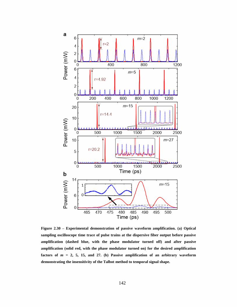
142
Figure 2.30 – Experimental demonstration of passive waveform amplification. (a) Optical
sampling oscilloscope time trace of pulse trains at the dispersive fiber output before passive
amplification (dashed blue, with the phase modulator turned off) and after passive
amplification (solid red, with the phase modulator turned on) for the desired amplification
factors of m = 2, 5, 15, and 27. (b) Passive amplification of an arbitrary waveform
demonstrating the insensitivity of the Talbot method to temporal signal shape.
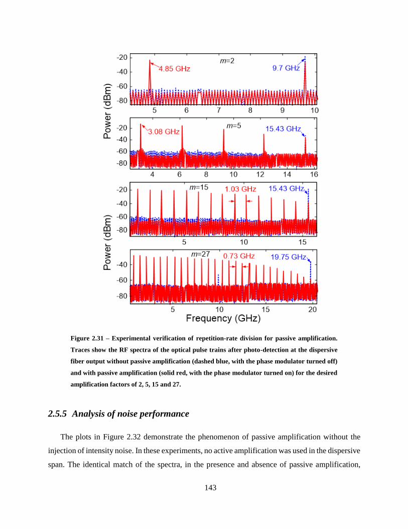
143
Figure 2.31 – Experimental verification of repetition-rate division for passive amplification.
Traces show the RF spectra of the optical pulse trains after photo-detection at the dispersive
fiber output without passive amplification (dashed blue, with the phase modulator turned off)
and with passive amplification (solid red, with the phase modulator turned on) for the desired
amplification factors of 2, 5, 15 and 27.
2.5.5 Analysis of noise performance
The plots in Figure 2.32 demonstrate the phenomenon of passive amplification without the
injection of intensity noise. In these experiments, no active amplification was used in the dispersive
span. The identical match of the spectra, in the presence and absence of passive amplification,
144
particularly at the noise-floor, indicates our technique does not contribute any measurable intensity
noise, consistent with what one would expect from a passive system. Using the spectral linear
interpolation method, the data show that the optical signal to noise ratio (OSNR) remains the same
in the presence of amplification. To be more concrete, Figure 2.32(a) shows the OSNR, in a 1 nm
resolution bandwidth of the optical spectrum analyzer, to be 50 dB without passive amplification,
PM-OFF (dashed blue), and 50 dB with passive amplification, PM-ON (red), indicating a noise
figure of 0 dB. Within our ability to measure OSNR, we show there is no injected intensity noise
from passive amplification.
On the other hand, when an active amplifier (EDFA) is used at the end of the same network
instead of passive amplification, the OSNR degrades from 50 dB to 36 dB, PM-OFF + EDFA (dot-
dashed green), due to the injected ASE noise from the active amplifier. Notice that all the spectra
traces are normalized to their respective amplitude peaks. The injected noise from active
amplification can also be inferred from the time traces shown in Figure 2.32(b). Although both
active and passive amplification amplify the peak of the signal by approximately 7 dB
(corresponding to passive gain of 5m and the equivalent active gain of 5), the active
amplification also raises the average noise floor by 7 dB (dot-dashed green) whereas passive
amplification leaves the floor at its original level (red). Figure 6c shows optical oscilloscope traces
with zero averaging, clearly confirming an increased fluctuation when active amplification is
employed (top trace) as compared to passive amplification (bottom trace).
Figure 2.33 shows enhancement of extinction ratio (ER) as the passive amplification factor m
increases for a noisy input with OSNR=10. In this experiment, ASE noise was injected onto the
pulse train in a controlled fashion using an EDFA, paired with a variable attenuator, at the input
of the phase modulator and placing two more EDFAs in the dispersive span. We define ER
enhancement as the ratio of the ER of the Talbot-amplified signal with respect to the ER of the
input train, where ER is given by the ratio of the average peak intensity of the waveform to the
average intensity of the noise floor.

145
Figure 2.32 – Experimental verification of noiseless amplification. (a) Optical spectra of the
pulse trains measured at the dispersive fiber output before passive amplification (phase
modulator turned off, PM-OFF), (dashed blue), after passive amplification (phase modulator
turned on, PM-ON) with m=5 (red), and with active amplification (EDFA) with gain of 5 (dot-
dashed green). Notice that all the spectra are normalized to their respective amplitude peaks.
(b)-(c) Corresponding optical sampling scope time traces in averaging mode and sampling
mode (no averaging), respectively.
Figure 2.33(a) shows simulated data (blue squares) of how the ER scales linearly with m , and
experimental data points for m 2, 5 and 15 overlaid (red triangles). The dashed blue line shows
the expected linear trend for ER enhancement. Passive amplification increases the waveform peak
146
intensity by m times, while leaving the noise floor at its average value. After phase modulation,
energy is distributed into m -times more frequency tones. After temporal redistribution by
dispersive delay, the individual frequency components of the waveform will add coherently to give
an average peak-power that is m -times the original signal. The noise floor, however, will remain
the same. This is shown clearly in the optical sampling scope trace in Figure 2.32(b), as well as
Figure 2.33(b) and (c), which show the optical sampling oscilloscope time traces with passive
amplification (red) and without (dashed blue) for 5m and 15m , respectively. Note that traces
in Figure 2.33(b) and (c) have been normalized to the same peak power rather than the noise floor
to better show ER enhancement. So long as the new frequency components generated during phase
modulation are the correct ones (dictated by a correct phase drive), the noise floor will have the
same average level from the destructive interference as before. Intensity noise present at the top of
the waveform signal will also keep the same average value through the passive amplification
process, in such a way that the ER enhancement actually increases linearly by a factor lower than
m (approaching m for a higher input OSNR).
Talbot amplification is not simply a time-domain equivalent of band-pass filtering (BPF) but
does actually redistribute signal energy from in-band noise. In order to show this important feature
of our technique, we additionally show data of Talbot amplification used in conjunction with band-
pass filtering and compare it to Talbot amplification without band-pass filtering, and to band-pass
filtering alone. Figure 2.33(a) shows the experimentally expected enhancement to ER when band-
pass filtering is employed without Talbot-amplification (solid violet). Here the filter used had a
nearly flat-top spectral response with a 40 dB bandwidth of 2.8nm. For this case of OSNR=10,
Figure 2.33(a) shows that BPF is better at enhancing the ER than passive amplification alone for
5m , and that it is equivalent for 15m . This can be also seen in the difference between the
solid red and dot-dashed green curves in Figure 2.33(b) and (c). However, when a BPF is used in
conjunction with Talbot amplification, the ER improves drastically since the BPF gets rid of the
out-of-band noise, and the passive amplification additionally enhances the resulting ER as
discussed above.
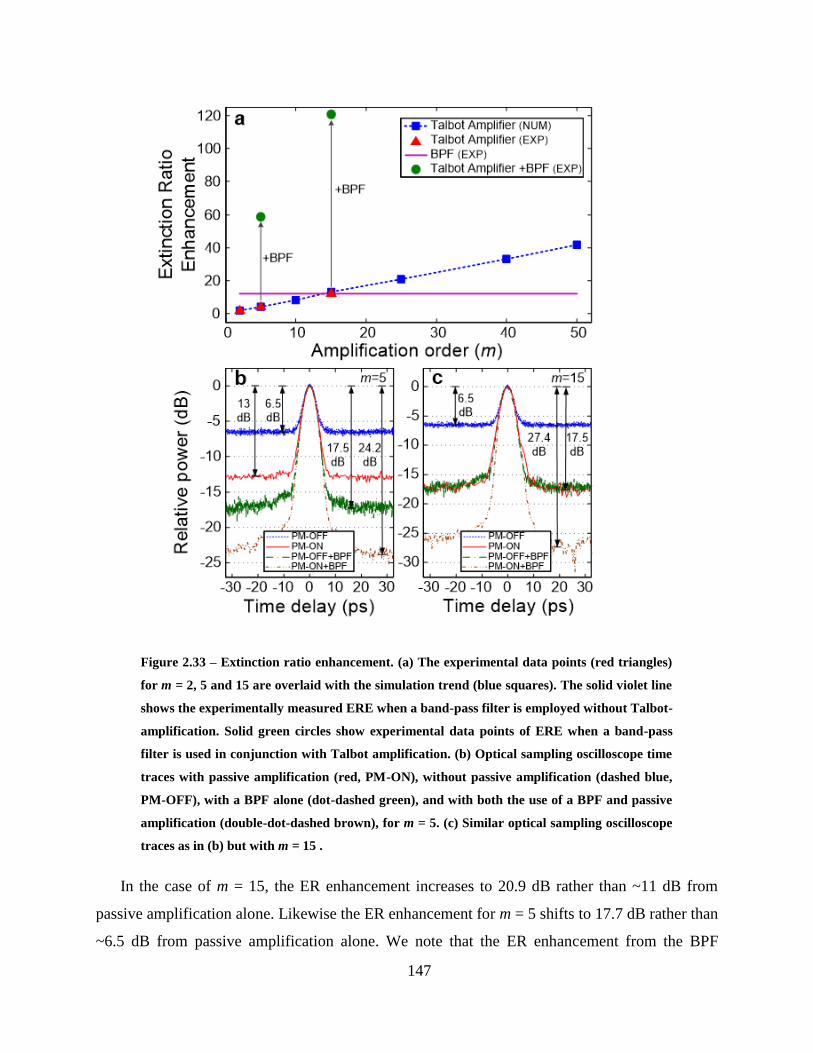
147
Figure 2.33 – Extinction ratio enhancement. (a) The experimental data points (red triangles)
for m = 2, 5 and 15 are overlaid with the simulation trend (blue squares). The solid violet line
shows the experimentally measured ERE when a band-pass filter is employed without Talbot-
amplification. Solid green circles show experimental data points of ERE when a band-pass
filter is used in conjunction with Talbot amplification. (b) Optical sampling oscilloscope time
traces with passive amplification (red, PM-ON), without passive amplification (dashed blue,
PM-OFF), with a BPF alone (dot-dashed green), and with both the use of a BPF and passive
amplification (double-dot-dashed brown), for m = 5. (c) Similar optical sampling oscilloscope
traces as in (b) but with m = 15 .
In the case of m = 15, the ER enhancement increases to 20.9 dB rather than ~11 dB from
passive amplification alone. Likewise the ER enhancement for m = 5 shifts to 17.7 dB rather than
~6.5 dB from passive amplification alone. We note that the ER enhancement from the BPF
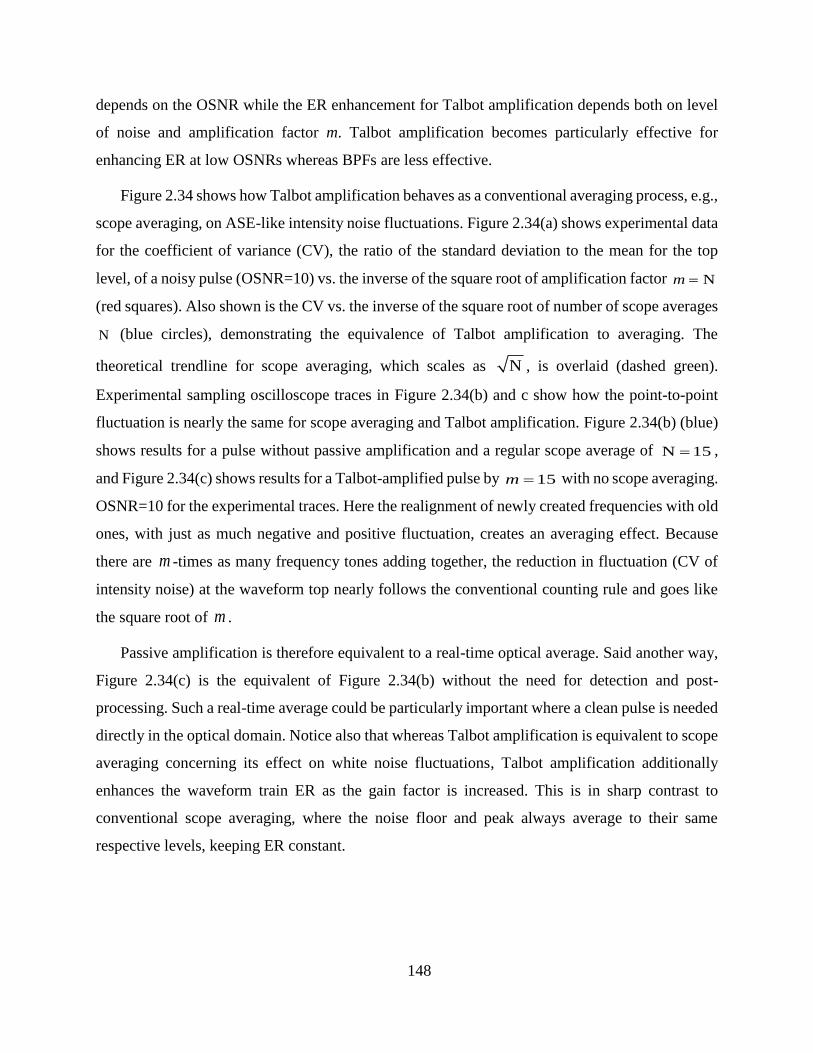
148
depends on the OSNR while the ER enhancement for Talbot amplification depends both on level
of noise and amplification factor m. Talbot amplification becomes particularly effective for
enhancing ER at low OSNRs whereas BPFs are less effective.
Figure 2.34 shows how Talbot amplification behaves as a conventional averaging process, e.g.,
scope averaging, on ASE-like intensity noise fluctuations. Figure 2.34(a) shows experimental data
for the coefficient of variance (CV), the ratio of the standard deviation to the mean for the top
level, of a noisy pulse (OSNR=10) vs. the inverse of the square root of amplification factor Nm
(red squares). Also shown is the CV vs. the inverse of the square root of number of scope averages
N (blue circles), demonstrating the equivalence of Talbot amplification to averaging. The
theoretical trendline for scope averaging, which scales as N , is overlaid (dashed green).
Experimental sampling oscilloscope traces in Figure 2.34(b) and c show how the point-to-point
fluctuation is nearly the same for scope averaging and Talbot amplification. Figure 2.34(b) (blue)
shows results for a pulse without passive amplification and a regular scope average of N 15 ,
and Figure 2.34(c) shows results for a Talbot-amplified pulse by 15m with no scope averaging.
OSNR=10 for the experimental traces. Here the realignment of newly created frequencies with old
ones, with just as much negative and positive fluctuation, creates an averaging effect. Because
there are m -times as many frequency tones adding together, the reduction in fluctuation (CV of
intensity noise) at the waveform top nearly follows the conventional counting rule and goes like
the square root of m .
Passive amplification is therefore equivalent to a real-time optical average. Said another way,
Figure 2.34(c) is the equivalent of Figure 2.34(b) without the need for detection and post-
processing. Such a real-time average could be particularly important where a clean pulse is needed
directly in the optical domain. Notice also that whereas Talbot amplification is equivalent to scope
averaging concerning its effect on white noise fluctuations, Talbot amplification additionally
enhances the waveform train ER as the gain factor is increased. This is in sharp contrast to
conventional scope averaging, where the noise floor and peak always average to their same
respective levels, keeping ER constant.
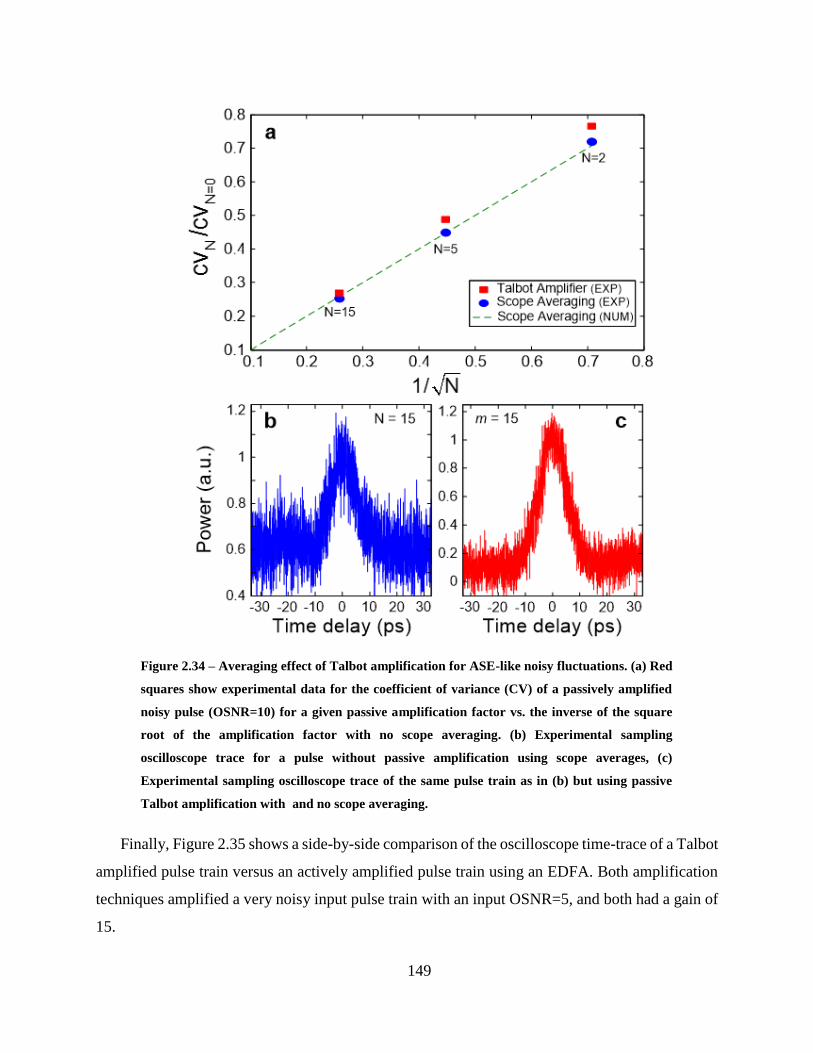
149
Figure 2.34 – Averaging effect of Talbot amplification for ASE-like noisy fluctuations. (a) Red
squares show experimental data for the coefficient of variance (CV) of a passively amplified
noisy pulse (OSNR=10) for a given passive amplification factor vs. the inverse of the square
root of the amplification factor with no scope averaging. (b) Experimental sampling
oscilloscope trace for a pulse without passive amplification using scope averages, (c)
Experimental sampling oscilloscope trace of the same pulse train as in (b) but using passive
Talbot amplification with and no scope averaging.
Finally, Figure 2.35 shows a side-by-side comparison of the oscilloscope time-trace of a Talbot
amplified pulse train versus an actively amplified pulse train using an EDFA. Both amplification
techniques amplified a very noisy input pulse train with an input OSNR=5, and both had a gain of
15.
150
Figure 2.35 – Comparison of passive and active amplification. Oscilloscope time-traces of (a) a
noisy pulse train (OSNR = 5) measured at the dispersive span output before passive
amplification (PM-OFF), (b) Oscilloscope time-trace of the noisy signal shown in trace (a) after
active amplification using an EDFA with a gain of 15, and (c) Oscilloscope time-trace of the
noisy signal shown in trace (a) after passive Talbot amplification (PM-ON) with passive gain
of 15.
The noisy input is shown in the top trace, and after active amplification, bottom trace, the pulse
is significantly degraded. Noise is injected onto the already-noisy train, and both the noise floor
and pulse peak are amplified about the same amount, negatively affecting the pulse quality.
However, in the case of passive amplification, no noise is injected, the ER is enhanced by a factor
approaching m - the peak is amplified while the noise floor is not, and the point-to-point
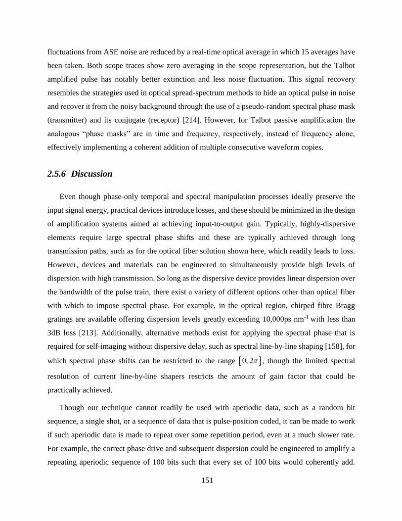
151
fluctuations from ASE noise are reduced by a real-time optical average in which 15 averages have
been taken. Both scope traces show zero averaging in the scope representation, but the Talbot
amplified pulse has notably better extinction and less noise fluctuation. This signal recovery
resembles the strategies used in optical spread-spectrum methods to hide an optical pulse in noise
and recover it from the noisy background through the use of a pseudo-random spectral phase mask
(transmitter) and its conjugate (receptor) [214]. However, for Talbot passive amplification the
analogous “phase masks” are in time and frequency, respectively, instead of frequency alone,
effectively implementing a coherent addition of multiple consecutive waveform copies.
2.5.6 Discussion
Even though phase-only temporal and spectral manipulation processes ideally preserve the
input signal energy, practical devices introduce losses, and these should be minimized in the design
of amplification systems aimed at achieving input-to-output gain. Typically, highly-dispersive
elements require large spectral phase shifts and these are typically achieved through long
transmission paths, such as for the optical fiber solution shown here, which readily leads to loss.
However, devices and materials can be engineered to simultaneously provide high levels of
dispersion with high transmission. So long as the dispersive device provides linear dispersion over
the bandwidth of the pulse train, there exist a variety of different options other than optical fiber
with which to impose spectral phase. For example, in the optical region, chirped fibre Bragg
gratings are available offering dispersion levels greatly exceeding 10,000ps nm-1 with less than
3dB loss [213]. Additionally, alternative methods exist for applying the spectral phase that is
required for self-imaging without dispersive delay, such as spectral line-by-line shaping [158], for
which spectral phase shifts can be restricted to the range 0, 2 , though the limited spectral
resolution of current line-by-line shapers restricts the amount of gain factor that could be
practically achieved.
Though our technique cannot readily be used with aperiodic data, such as a random bit
sequence, a single shot, or a sequence of data that is pulse-position coded, it can be made to work
if such aperiodic data is made to repeat over some repetition period, even at a much slower rate.
For example, the correct phase drive and subsequent dispersion could be engineered to amplify a
repeating aperiodic sequence of 100 bits such that every set of 100 bits would coherently add.
152
Alternatively, one could purposely modulate data at a faster rate in order to use Talbot-
amplification to coherently add and amplify it at a slower desired output rate. Though our
technique cannot generally be applied to data sequences, there are important exceptions where it
can be engineered to work.
Because dispersion in many wave systems can be controlled along wave propagation (as in the
case of optical fibre links shown here), our method can also be used to tailor amplification to occur
only at specific locations far away from any power source, offering the unique possibility of remote
or localized waveform amplification. Perhaps of greater significance is how passive amplification
using our method can be readily applied to other spectral regions or wave systems. Passive
amplification by self-imaging is applicable to any wave system in which the temporal and
dispersive spectral phase can be controlled. Such control is not only available throughout the entire
electromagnetic spectrum [215], but also for many other wave systems, such as acoustic [216] and
matter waves [217, 218], for which active gain mechanisms are extremely challenging to
implement or simply not available. For example, direct passive amplification of acoustic and
vibrational waveforms without the need for transducers could be useful in micro-electro-
mechanical systems (MEMS) design [219], sonar, and ultrasonic sensing and imaging.
Additionally, passive probability amplification of matter-waves could provide another tool for
atom optics to control and manipulate quantum states of matter [217, 218] as well as single photon
pulses [220].
2.5.7 Conclusion
In summary, we have proposed and experimentally demonstrated a new concept for waveform
intensity amplification without using active gain by recycling energy already stored in the input
signal. Our method uses dispersive self-imaging phenomena, temporal Talbot effects, which
exploit the intrinsic repetitive nature of waveform signals to precisely redistribute the input signal
energy into fewer waveforms in order to achieve noiseless amplification of each individual
waveform. This technique allows us to overcome critical limitations of present active-gain based
amplification methods. In particular, our demonstrated passive waveform amplification technique
represents an amplification method that can be potentially applied to repetitive signals in all wave
systems, eliminates the wasted power inherent in applications requiring peak-power amplification,
153
does not amplify or inject noise in the output signal, and even enhances the extinction ratio and
reduces noise fluctuation of the input waveform train.
2.5.8 Methods
A. Optical waveform generation and phase modulation
We used a commercial actively mode-locked fibre laser (Pritel - Ultrafast Optical Clock) to
generate a repetitive input optical pulse train with tunable repetition-rate. Temporal pulses directly
generated from the laser are Gaussian in shape, approximately 7.0 ps intensity full width at half
maximum (FWHM). Generation of optical pulses with a sinc-like temporal shape was achieved by
filtering the input pulse train with a square-spectrum filtering function using an optical wave-
shaper (Finisar 4000S). The appropriate multilevel temporal phase modulation required for a
desired amplification factor was applied to the optical pulses with a commercial fibre-integrated
electro-optic phase modulator (EOspace, 25 GHz bandwidth) driven by an electronic arbitrary
waveform generator (Tektronix AWG7122C, 7.5 GHz analog bandwidth).
B. Dispersive medium
The subsequent first-order dispersion was provided by six dispersion-compensating fibre
modules (Corning PureForm DCM-D-080-04), with a total of ~8,000ps nm-1 for m = 15 and m =
27 and ~2,650ps nm-1 for m = 2 and m = 5. Each module had a loss of 7 dB. Because the amount
of dispersion required for coherent addition grows linearly with the desired amplification factor
and quadratically with the temporal period of the repeating input waveform, changing the
repetition-rate of the input pulse train allowed us the experimental convenience of demonstrating
different amplification factors at the output of the similar length of dispersive optical fibre link.
C. Noise emulation
For noise mitigation experiments, ASE noise was purposely injected onto the pulse train using
an EDFA at the input of the phase modulator and placing two additional EDFAs in the dispersive
span. Using a variable attenuator prior to the input EDFA, we controlled the input power, versus
the fixed amount of injected ASE noise from the EDFAs in the system, thereby implementing a
desired value of OSNR. For simulation, noise was modeled in the frequency-domain as random
Gaussian fluctuation in both phase and amplitude, with mean spectral amplitude- and phase-noise
154
components as zero and a standard deviation per frequency point normalized to sum to the desired
average noise power, and corresponding desired OSNR.
D. Optical characterization
All optical time-traces were recorded with a 500-GHz bandwidth optical sampling oscilloscope
(Exfo PSO-100), the optical spectra were recorded with high-resolution (20-MHz) optical
spectrum analyzer (Apex, AP2440A), the RF phase drive was recorded with a 40-GHz bandwidth
electrical sampling oscilloscope (Tektronix CSA8200), and RF spectra were recorded by detecting
the optical pulse train with a 45-GHz photo-detector (New Focus Model 1014) which was then
input into a 26-GHz RF spectrum analyzer (HP 8563E).

155
Chapter 3
3 Energy-Efficient Optical Signal
Processors
3.1 Introduction
In this Chapter, we develop novel energy-efficient signal processing concepts and technologies
for optical data signals used for telecom applications. For this purpose, we define, design, and
develop two relevant set of processing approaches: (i) novel approaches for base-rate and sub-
harmonic clock recovery of on-off-keying (OOK) data signals. The former is implemented based
on phase-only linear optical filtering of the incoming RZ signal (Section 3.2), whereas the latter
exploits the so-called ‘inverse’ self-imaging effect (Section 3.3). (ii) a novel approach for all
optical return-to-zero (RZ)-to-non-RZ (NRZ) telecommunication data format conversion, which
has been experimentally implemented at a bit rate of 640 Gbit/s. In this approach, we show how a
proper phase-only manipulation of the frequency content of a RZ data signal can be used to
implement conversion of the RZ signal into the equivalent NRZ time-domain data (Section 3.4).
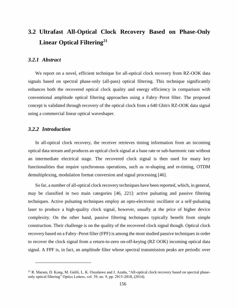
156
3.2 Ultrafast All-Optical Clock Recovery Based on Phase-Only
Linear Optical Filtering21
3.2.1 Abstract
We report on a novel, efficient technique for all-optical clock recovery from RZ-OOK data
signals based on spectral phase-only (all-pass) optical filtering. This technique significantly
enhances both the recovered optical clock quality and energy efficiency in comparison with
conventional amplitude optical filtering approaches using a Fabry–Perot filter. The proposed
concept is validated through recovery of the optical clock from a 640 Gbit/s RZ-OOK data signal
using a commercial linear optical waveshaper.
3.2.2 Introduction
In all-optical clock recovery, the receiver retrieves timing information from an incoming
optical data stream and produces an optical clock signal at a base rate or sub-harmonic rate without
an intermediate electrical stage. The recovered clock signal is then used for many key
functionalities that require synchronous operations, such as re-shaping and re-timing, OTDM
demultiplexing, modulation format conversion and signal processing [46].
So far, a number of all-optical clock recovery techniques have been reported, which, in general,
may be classified in two main categories [46, 221]: active pulsating and passive filtering
techniques. Active pulsating techniques employ an opto-electronic oscillator or a self-pulsating
laser to produce a high-quality clock signal, however, usually at the price of higher device
complexity. On the other hand, passive filtering techniques typically benefit from simple
construction. Their challenge is on the quality of the recovered clock signal though. Optical clock
recovery based on a Fabry–Perot filter (FPF) is among the most studied passive techniques in order
to recover the clock signal from a return-to-zero on-off-keying (RZ OOK) incoming optical data
signal. A FPF is, in fact, an amplitude filter whose spectral transmission peaks are periodic over
21 R. Maram, D. Kong, M. Galili, L. K. Oxenløwe and J. Azaña, “All-optical clock recovery based on spectral phase-
only optical filtering” Optics Letters, vol. 39, no. 9, pp. 2815-2818, (2014).
157
the optical frequency bandwidth of interest and where the transmission spectral bands are typically
narrow. This filter, with a free spectral range (FSR) tuned to the bit rate of the incoming optical
data signal, preserves the discrete clock spectral components from the incoming optical data signal
and removes the rest of the signal’s continuous spectral content, which typically contains around
50% of the overall energy of the incoming data signal. Since a FPF is a fully passive device, the
operation speed of techniques based on FPF is ideally unlimited. However, to achieve a high-
quality clock signal, a high finesse FPF is required to average out the incoming data pattern. The
needed high finesse imposes a very stringent tolerance for mismatching between the filter
specifications (resonant frequency and FSR) and the incoming data signal specifications (central
wavelength and bit rate, respectively). On the other hand, a lower FPF finesse leads to amplitude
modulation (AM) in the clock signal. To minimize this AM, the FPF should be followed by a
nonlinear subsystem [46], e.g., a semiconductor optical amplifier (SOA), an ultrafast nonlinear
interferometer or a Mach–Zehnder interferometer, acting as an optical power equalizer. Not only
does this increase the clock-recovery circuit complexity but additionally, these subsystems may
limit the system operating data rate, e.g. to tens of Gbit/s when using SOAs.
In this paper, we demonstrate a novel, simple passive all-optical clock recovery technique
based on spectral phase-only (all-pass) optical filtering for RZ-OOK data signals. This technique
overcomes the above-mentioned crucial drawbacks of the FPF method. In particular, the proposed
technique offers a significantly improved performance, e.g. leading to significantly smaller AM in
the recovered clock signal for similar filter specifications (particularly finesse), in comparison to
an amplitude filter, such as a FPF. It also provides higher energy efficiency, at least a two-fold
improvement, since fundamentally no signal energy is lost in the phase-only optical filtering
process. The novel scheme is demonstrated using numerical simulations and through a successful
proof-of-concept all-optical clock recovery experiment on a 640 Gbit/s data signal using a
commercial linear optical waveshaper.
3.2.3 The operation principle
All-optical clock recovery of an RZ-OOK data signal can be achieved by extracting the discrete
clock spectral components of the incoming signal, which implies suppressing the continuous
frequency content of the signal optical spectrum. A periodic optical amplitude filter whose FSR is
158
matched to the signal bit rate (f0) and a sufficiently narrow spectral line-width (Fb), i.e., high finesse
(= FSR/Fb), can effectively implement this operation, as shown in Figure 3.1, left.
Amplitude Filter
RZ Input
t
f
0f
.F
t
f
0f
1 .F
Phase-only Filter
Output
t
f
0f
1 .F
Output
f
FSRbF
Amplitude Phase f
FSRbF
Amplitude Phase
Figure 3.1 – Principle of the optical clock recovery methods based on amplitude (left) and
phase-only (right) filtering. F stands for Fourier transform.
In this clock recovery process, approximately 50% of the energy of the input optical signal is
lost in order to extract the desired optical clock signal. Additionally, the extracted signal also
suffers from an increased amplitude modulation (AM: highest to lowest pulse ratio) as the finesse
of the filter is decreased, i.e. as the spectral line-width Fb is increased. However, we show here
that a spectrally periodic phase-only filter can be properly designed to achieve the same clock
recovery result with significantly reduced AM, for the same value of filter finesse (defined now as
the spectral phase line-width), and without removing any spectral component of the input signal
and hence, without fundamentally losing any energy in the filtering process. Figure 3.1, right,
shows schematically the spectral phase profile of the proposed all-pass filter: the discrete clock
spectral components in the input optical signal must be phase shifted by π/2 with respect to the rest
of the signal spectrum. Thus, the FSR of the spectral phase profile must be also fixed to match the
data signal bit rate. Indeed, the operation principle of the phase filtering technique is inspired from
the amplitude filtering approach, in which the extraction of either the discrete clock spectral
159
components or continuous spectral content leads to the creation of periodic optical pulse trains
along the time domain. However, in the former, all pulses are in-phase whereas in the latter, pulses
are phase-shifted by π in the temporal locations corresponding to the “zeros” of the input signal.
In the reverse direction, summation of these pulse trains will retrieve the input signal. However,
in the phase filtering approach, the temporal periodic pulses corresponding to the discrete clock
components and continuous spectral content are all phase-shifted by π/2 with respect to each other.
Thus, the two components beat in intensity leading to the observed generation of the periodic
optical clock pulse train. The defined phase filtering can be practically implemented using a variety
of technologies such as line-by-line optical pulse shapers, Fiber Bragg Gratings (FBG), thin film
filters, photonic ring resonators, and photonic crystals, among others [222]. Polarization-
independent clock recovery can be achieved as long as a polarization-insensitive optical filtering
technology is used. In the experiment reported here, we use a line-by-line optical pulse shaper,
which allows for high-resolution, independent manipulation of the phase of the individual spectral
lines. Line-by-line pulse shapers with frequency resolutions (Fb) as low as ~890 MHz have been
reported [223].
3.2.4 Performance analysis and simulation results
The described operation principle has been first validated and compared with the use of a FPF
with similar filtering specifications (shape, FSR and finesse, ignoring insertion loss) through
numerical simulations based on the standard frequency-domain method for linear processes.
Figure 3.2 shows the transmission spectrum and spectral phase of the used (a) FPF and (b) phase
filter, respectively. The finesse of the two filters is assumed to be 103. As for the input data signal,
we assume RZ-OOK data with a pseudorandom bit sequence (PRBS) of 27-1 bits, 400-fs FWHM
Gaussian pulses, with peak power of 100 mW, and a bit rate of 640 Gbit/s.
Figure 3.3 presents the simulation results of all-optical clock recovery from the 640 Gbit/s
input signal. Each row shows temporal waveform and optical spectrum of the input signal ((a) and
(b)), the recovered optical clock after the FPF ((c) and (d)), and the recovered clock after the phase
filter ((e) and (f)), respectively.
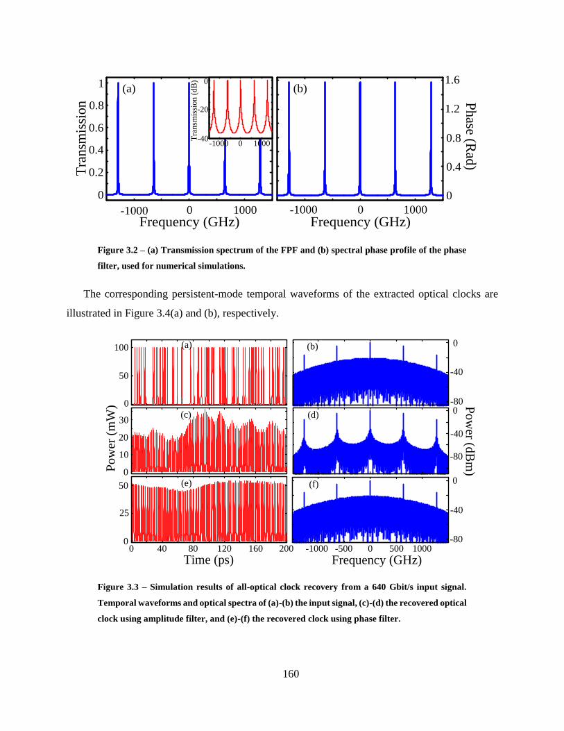
160
(a) (b)
-1000 0 1000
0
0.2
0.4
0.6
0.8
1
-1000 0 1000-40
-20
0T
ransm
issi
on
Tra
nsm
issi
on
(d
B)
-1000 0 1000
0
0.4
0.8
1.2
1.6
Phase (R
ad)
Frequency (GHz)Frequency (GHz)
Figure 3.2 – (a) Transmission spectrum of the FPF and (b) spectral phase profile of the phase
filter, used for numerical simulations.
The corresponding persistent-mode temporal waveforms of the extracted optical clocks are
illustrated in Figure 3.4(a) and (b), respectively.
Pow
er (
mW
)
Time (ps) Frequency (GHz)
0
50
100
0
10
20
30
0 40 80 120 160 2000
25
50
-80
-40
0
-80
-40
0
-1000 -500 0 500 1000-80
-40
0
Pow
er (dB
m)
(e) (f)
(c) (d)
(b)(a)
Figure 3.3 – Simulation results of all-optical clock recovery from a 640 Gbit/s input signal.
Temporal waveforms and optical spectra of (a)-(b) the input signal, (c)-(d) the recovered optical
clock using amplitude filter, and (e)-(f) the recovered clock using phase filter.
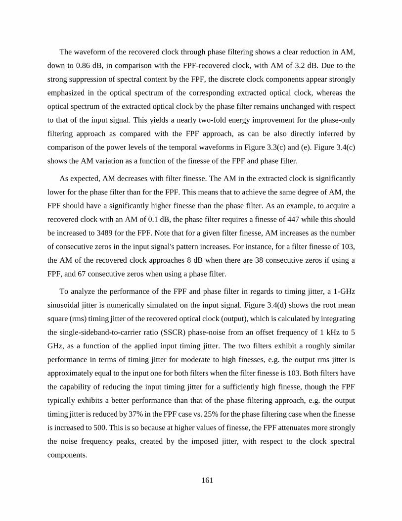
161
The waveform of the recovered clock through phase filtering shows a clear reduction in AM,
down to 0.86 dB, in comparison with the FPF-recovered clock, with AM of 3.2 dB. Due to the
strong suppression of spectral content by the FPF, the discrete clock components appear strongly
emphasized in the optical spectrum of the corresponding extracted optical clock, whereas the
optical spectrum of the extracted optical clock by the phase filter remains unchanged with respect
to that of the input signal. This yields a nearly two-fold energy improvement for the phase-only
filtering approach as compared with the FPF approach, as can be also directly inferred by
comparison of the power levels of the temporal waveforms in Figure 3.3(c) and (e). Figure 3.4(c)
shows the AM variation as a function of the finesse of the FPF and phase filter.
As expected, AM decreases with filter finesse. The AM in the extracted clock is significantly
lower for the phase filter than for the FPF. This means that to achieve the same degree of AM, the
FPF should have a significantly higher finesse than the phase filter. As an example, to acquire a
recovered clock with an AM of 0.1 dB, the phase filter requires a finesse of 447 while this should
be increased to 3489 for the FPF. Note that for a given filter finesse, AM increases as the number
of consecutive zeros in the input signal's pattern increases. For instance, for a filter finesse of 103,
the AM of the recovered clock approaches 8 dB when there are 38 consecutive zeros if using a
FPF, and 67 consecutive zeros when using a phase filter.
To analyze the performance of the FPF and phase filter in regards to timing jitter, a 1-GHz
sinusoidal jitter is numerically simulated on the input signal. Figure 3.4(d) shows the root mean
square (rms) timing jitter of the recovered optical clock (output), which is calculated by integrating
the single-sideband-to-carrier ratio (SSCR) phase-noise from an offset frequency of 1 kHz to 5
GHz, as a function of the applied input timing jitter. The two filters exhibit a roughly similar
performance in terms of timing jitter for moderate to high finesses, e.g. the output rms jitter is
approximately equal to the input one for both filters when the filter finesse is 103. Both filters have
the capability of reducing the input timing jitter for a sufficiently high finesse, though the FPF
typically exhibits a better performance than that of the phase filtering approach, e.g. the output
timing jitter is reduced by 37% in the FPF case vs. 25% for the phase filtering case when the finesse
is increased to 500. This is so because at higher values of finesse, the FPF attenuates more strongly
the noise frequency peaks, created by the imposed jitter, with respect to the clock spectral
components.
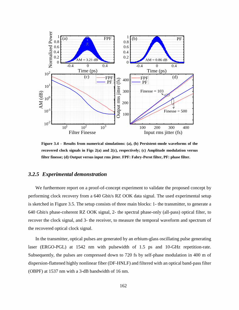
162
(b)
Filter Finesse
AM
(d
B)
310110
2
10-1
100
101
10
102
10-2
FPFPF
(c)
100 200 300 400
100
200
300
400
Ou
tpu
t rm
s ji
tter
(fs
)
Finesse = 103
Finesse = 500
FPFPF
Input rms jitter (fs)
AM = 0.86 dB0
0.2
0.4
0.6
0.8
1
Time (ps)-0.4 0 0.4N
orm
aliz
ed P
ow
er
(a) FPF
AM = 3.21 dB0
0.2
0.4
0.6
0.8
1
Time (ps)-0.4 0 0.4
(d)
PF
Figure 3.4 – Results from numerical simulations: (a), (b) Persistent-mode waveforms of the
recovered clock signals in Figs 2(a) and 2(c), respectively; (c) Amplitude modulation versus
filter finesse; (d) Output versus input rms jitter. FPF: Fabry-Perot filter, PF: phase filter.
3.2.5 Experimental demonstration
We furthermore report on a proof-of-concept experiment to validate the proposed concept by
performing clock recovery from a 640 Gbit/s RZ OOK data signal. The used experimental setup
is sketched in Figure 3.5. The setup consists of three main blocks: 1- the transmitter, to generate a
640 Gbit/s phase-coherent RZ OOK signal, 2- the spectral phase-only (all-pass) optical filter, to
recover the clock signal, and 3- the receiver, to measure the temporal waveform and spectrum of
the recovered optical clock signal.
In the transmitter, optical pulses are generated by an erbium-glass oscillating pulse generating
laser (ERGO-PGL) at 1542 nm with pulsewidth of 1.5 ps and 10-GHz repetition-rate.
Subsequently, the pulses are compressed down to 720 fs by self-phase modulation in 400 m of
dispersion-flattened highly nonlinear fiber (DF-HNLF) and filtered with an optical band-pass filter
(OBPF) at 1537 nm with a 3-dB bandwidth of 16 nm.
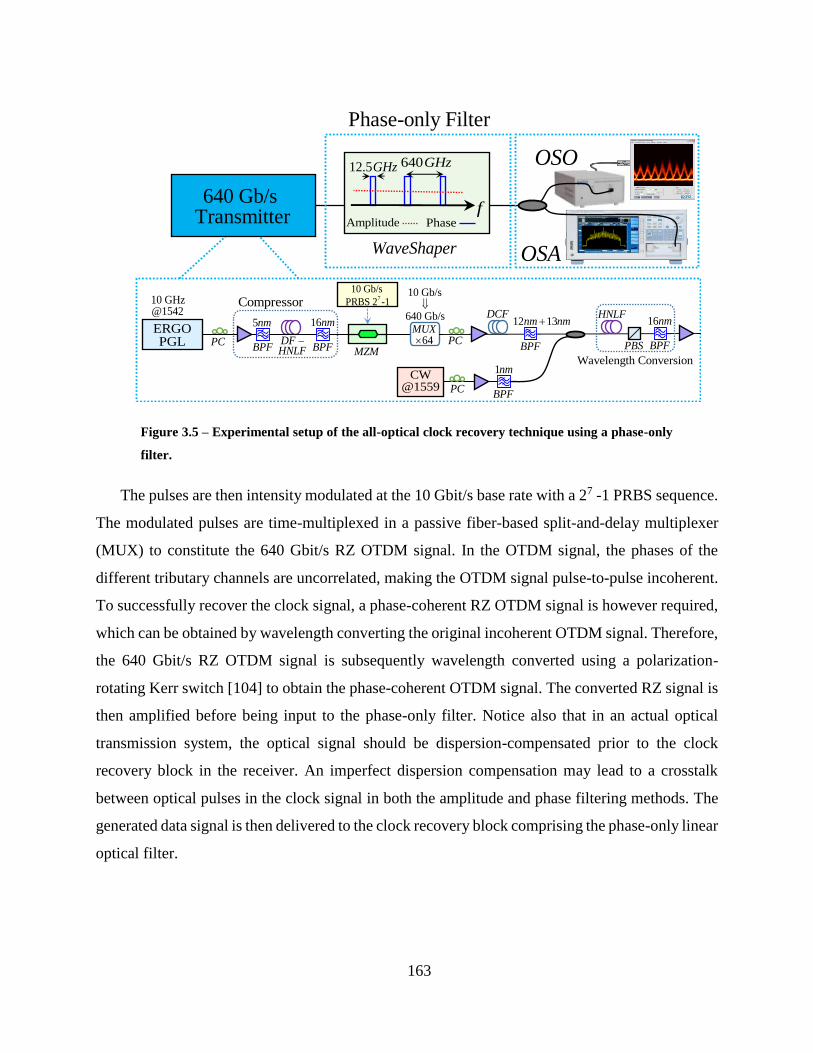
163
OSO
Phase-only Filter
WaveShaper OSA
f
640GHz
Amplitude Phase
12.5GHz
640 Gb/s Transmitter
ERGOPGL
10 GHz@1542
Compressor
5nm 16nm
BPF BPFPC
7
10 Gb/s
PRBS 2 -110 Gb/s
640 Gb/s
DFHNLF
MZM
64MUX
CW@1559
Wavelength Conversion
DCF
BPF
12 13nm nm
BPF
1nm
HNLF
PBS BPF
16nm
PC
PC
Figure 3.5 – Experimental setup of the all-optical clock recovery technique using a phase-only
filter.
The pulses are then intensity modulated at the 10 Gbit/s base rate with a 27 -1 PRBS sequence.
The modulated pulses are time-multiplexed in a passive fiber-based split-and-delay multiplexer
(MUX) to constitute the 640 Gbit/s RZ OTDM signal. In the OTDM signal, the phases of the
different tributary channels are uncorrelated, making the OTDM signal pulse-to-pulse incoherent.
To successfully recover the clock signal, a phase-coherent RZ OTDM signal is however required,
which can be obtained by wavelength converting the original incoherent OTDM signal. Therefore,
the 640 Gbit/s RZ OTDM signal is subsequently wavelength converted using a polarization-
rotating Kerr switch [104] to obtain the phase-coherent OTDM signal. The converted RZ signal is
then amplified before being input to the phase-only filter. Notice also that in an actual optical
transmission system, the optical signal should be dispersion-compensated prior to the clock
recovery block in the receiver. An imperfect dispersion compensation may lead to a crosstalk
between optical pulses in the clock signal in both the amplitude and phase filtering methods. The
generated data signal is then delivered to the clock recovery block comprising the phase-only linear
optical filter.
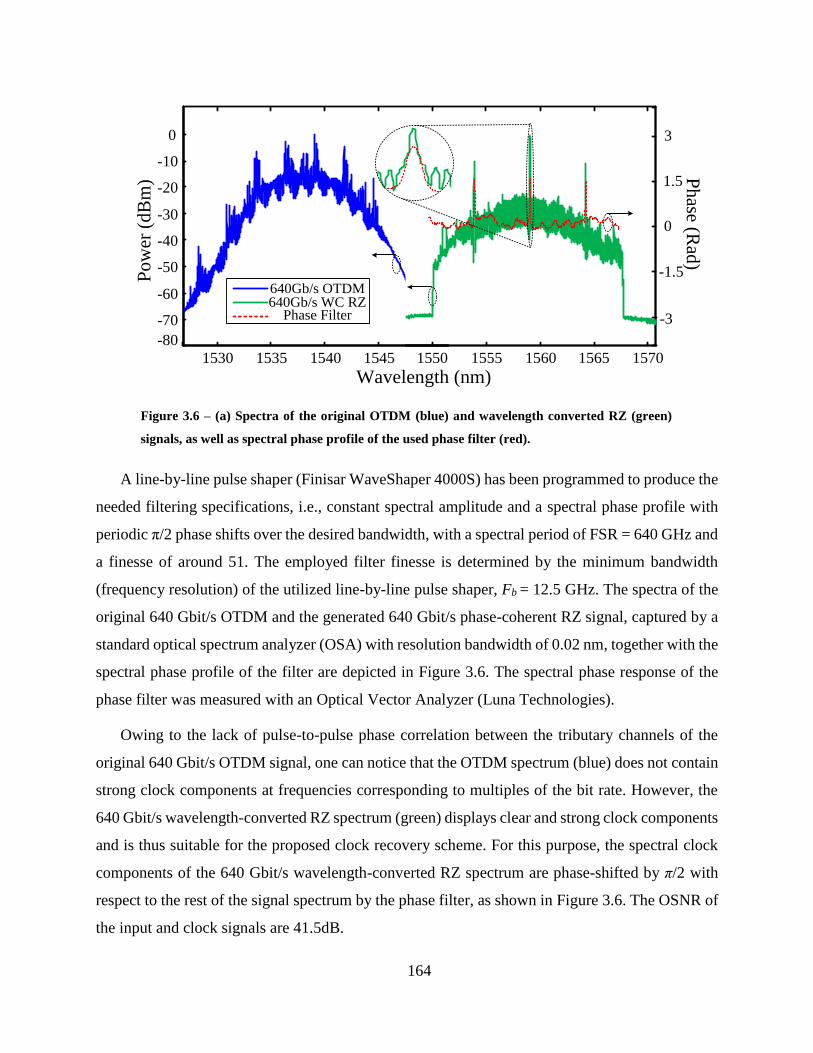
164
-80
-70
-60
-50
-40
-30
-20
-10
0
1550 1555 1560 1565 15701545154015351530
Wavelength (nm)
Po
wer
(d
Bm
) Ph
ase (Rad
)
0
1.5
-1.5
-3
3
640Gb/s OTDM640Gb/s WC RZ
Phase Filter
Figure 3.6 – (a) Spectra of the original OTDM (blue) and wavelength converted RZ (green)
signals, as well as spectral phase profile of the used phase filter (red).
A line-by-line pulse shaper (Finisar WaveShaper 4000S) has been programmed to produce the
needed filtering specifications, i.e., constant spectral amplitude and a spectral phase profile with
periodic π/2 phase shifts over the desired bandwidth, with a spectral period of FSR = 640 GHz and
a finesse of around 51. The employed filter finesse is determined by the minimum bandwidth
(frequency resolution) of the utilized line-by-line pulse shaper, Fb = 12.5 GHz. The spectra of the
original 640 Gbit/s OTDM and the generated 640 Gbit/s phase-coherent RZ signal, captured by a
standard optical spectrum analyzer (OSA) with resolution bandwidth of 0.02 nm, together with the
spectral phase profile of the filter are depicted in Figure 3.6. The spectral phase response of the
phase filter was measured with an Optical Vector Analyzer (Luna Technologies).
Owing to the lack of pulse-to-pulse phase correlation between the tributary channels of the
original 640 Gbit/s OTDM signal, one can notice that the OTDM spectrum (blue) does not contain
strong clock components at frequencies corresponding to multiples of the bit rate. However, the
640 Gbit/s wavelength-converted RZ spectrum (green) displays clear and strong clock components
and is thus suitable for the proposed clock recovery scheme. For this purpose, the spectral clock
components of the 640 Gbit/s wavelength-converted RZ spectrum are phase-shifted by π/2 with
respect to the rest of the signal spectrum by the phase filter, as shown in Figure 3.6. The OSNR of
the input and clock signals are 41.5dB.
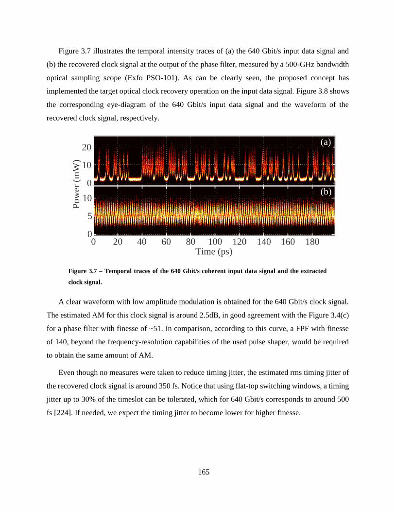
165
Figure 3.7 illustrates the temporal intensity traces of (a) the 640 Gbit/s input data signal and
(b) the recovered clock signal at the output of the phase filter, measured by a 500-GHz bandwidth
optical sampling scope (Exfo PSO-101). As can be clearly seen, the proposed concept has
implemented the target optical clock recovery operation on the input data signal. Figure 3.8 shows
the corresponding eye-diagram of the 640 Gbit/s input data signal and the waveform of the
recovered clock signal, respectively.
0
Time (ps)
Po
wer
(m
W)
0 20 40 60 80 100 120 140 160 180
10
5
0
20
10
(a)
(b)
Figure 3.7 – Temporal traces of the 640 Gbit/s coherent input data signal and the extracted
clock signal.
A clear waveform with low amplitude modulation is obtained for the 640 Gbit/s clock signal.
The estimated AM for this clock signal is around 2.5dB, in good agreement with the Figure 3.4(c)
for a phase filter with finesse of ~51. In comparison, according to this curve, a FPF with finesse
of 140, beyond the frequency-resolution capabilities of the used pulse shaper, would be required
to obtain the same amount of AM.
Even though no measures were taken to reduce timing jitter, the estimated rms timing jitter of
the recovered clock signal is around 350 fs. Notice that using flat-top switching windows, a timing
jitter up to 30% of the timeslot can be tolerated, which for 640 Gbit/s corresponds to around 500
fs [224]. If needed, we expect the timing jitter to become lower for higher finesse.
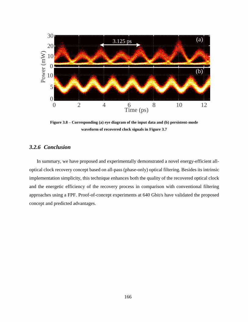
166
Time (ps)
Po
wer
(m
W)
0 2 4 6 8 10 12
10
5
0
30
20
10
0
(a)
(b)
3.125 ps
Figure 3.8 – Corresponding (a) eye diagram of the input data and (b) persistent-mode
waveform of recovered clock signals in Figure 3.7
3.2.6 Conclusion
In summary, we have proposed and experimentally demonstrated a novel energy-efficient all-
optical clock recovery concept based on all-pass (phase-only) optical filtering. Besides its intrinsic
implementation simplicity, this technique enhances both the quality of the recovered optical clock
and the energetic efficiency of the recovery process in comparison with conventional filtering
approaches using a FPF. Proof-of-concept experiments at 640 Gbit/s have validated the proposed
concept and predicted advantages.

167
3.3 Sub-harmonic periodic pulse train recovery from aperiodic
optical pulse sequences through dispersion-induced temporal
self-imaging22
3.3.1 Abstract
Temporal self-imaging effects (TSIs) are observed when a periodic pulse train propagates
through a first-order dispersive medium. Under specific dispersion conditions, either an exact, rate
multiplied or rate divided image of the input signal is reproduced at the output. TSI possesses an
interesting self-restoration capability even when acting over an aperiodic train of pulses. In this
work, we investigate and demonstrate, for the first time to our knowledge, the capability of TSI to
produce periodic sub-harmonic (rate-divided) pulse trains from aperiodic sequences. We use this
inherent property of the TSI to implement a novel, simple and reconfigurable sub-harmonic optical
clock recovery technique from RZ-OOK data signals. The proposed technique features a very
simple realization, involving only temporal phase modulation and first-order dispersion and it
allows one to set the repetition-rate of the reconstructed clock signal in integer fractions (sub-
harmonics) of the input bit rate. Proof-of-concept experiments are reported to validate the proposed
technique and guidelines for optimization of the clock-recovery process are also outlined.
3.3.2 Introduction
The temporal self-imaging effect (TSI), also referred to as temporal Talbot effect, is the time-
domain counterpart of the well-known spatial self-imaging phenomenon [41, 135]. This space-
time duality is related to the mathematical isomorphism existing between the equations describing
the paraxial diffraction of beams in space and the first-order temporal dispersion of optical pulses.
The TSI occurs when a periodic train of optical pulses propagates through a dispersive medium in
a first-order approximation; such a dispersive medium is characterized by a linear all-pass
amplitude response and a quadratic phase variation in frequency. An appropriate amount of
22 R. Maram, L. Romero Cortés and J. Azaña, “Sub-harmonic periodic pulse train recovery from aperiodic pulse trains
through dispersion-induced temporal self-imaging,” Optics Express, vol. 23, no. 3, pp. 3602-3613, (2015).
168
dispersion, given by the so-called self-imaging condition [41, 135], leads to either an exact
reproduction of the original pulse train (integer TSI) or to repetition-rate multiplication by an
integer factor (fractional TSI).
Besides the intrinsic physical interest of the TSI phenomenon, it has also been put into practical
use in several areas. In particular, TSI has been extensively studied as a lossless mean to multiply
the repetition-rate of a periodic pulse train, through fractional TSI [41, 135, 158, 185, 225, 226,
227]. This phenomenon also has been investigated theoretically to be an accurate technique for
measuring the first-order dispersion coefficient of dispersive media [135]. Moreover, Pudo et al.
[100, 99] have shown the inherent buffering ability of TSI to generate a periodic output, even from
an aperiodic input pulse train. They have used this property to perform base-rate clock recovery
(BRCR) of a return-to-zero on–off keying (RZ-OOK) optical data signal by utilizing single-mode
fibers (SMFs) or linearly chirped fiber Bragg gratings (LCFBGs) as dispersive media.
Very recently a new feature of TSI, referred here to as inverse temporal self-imaging (I-TSI),
has been reported to demonstrate passive amplification of repetitive optical signals [188]. I-TSI
involves repetition-rate division of an incoming repetitive pulse train by an integer factor (m = 2,
3, …) through an ideally lossless redistribution of the input signal energy, effectively
implementing a process equivalent to coherent addition of each m individual consecutive pulses.
Similar to the TSI, the I-TSI is based on the distributed interference of dispersed pulses, i.e., there
is no direct one-to-one correspondence between the input and output pulses. As a consequence, we
anticipate that this effect should also possess the inherent property to generate a periodic output
(with sub-harmonic repetition-rate), yet from an aperiodic input pulse train. This feature, therefore,
could be appropriately used to recover the m-sub-harmonic clock signal of a RZ-OOK data signal.
In optical communications, optical sub-harmonic clock recovery (SHCR) is a fundamental
functionality for de-multiplexing optical time-division multiplexed (OTDM) systems and
subsequent processing operations [228, 229, 94, 230].
In this paper, we propose and experimentally demonstrate the realization of a reconfigurable
SHCR technique based on I-TSI. The proposed concept can be implemented using a very simple
setup, involving a suitable combination of temporal phase modulation and dispersive spectral
phase filtering of the original aperiodic (data) pulse train. This setup can be designed to reconstruct
a periodic optical pulse train (clock) in which the pulses are spaced by m times the bit period of
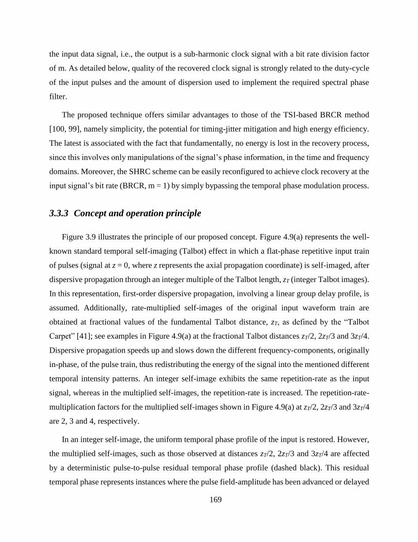
169
the input data signal, i.e., the output is a sub-harmonic clock signal with a bit rate division factor
of m. As detailed below, quality of the recovered clock signal is strongly related to the duty-cycle
of the input pulses and the amount of dispersion used to implement the required spectral phase
filter.
The proposed technique offers similar advantages to those of the TSI-based BRCR method
[100, 99], namely simplicity, the potential for timing-jitter mitigation and high energy efficiency.
The latest is associated with the fact that fundamentally, no energy is lost in the recovery process,
since this involves only manipulations of the signal’s phase information, in the time and frequency
domains. Moreover, the SHRC scheme can be easily reconfigured to achieve clock recovery at the
input signal’s bit rate (BRCR, m = 1) by simply bypassing the temporal phase modulation process.
3.3.3 Concept and operation principle
Figure 3.9 illustrates the principle of our proposed concept. Figure 4.9(a) represents the well-
known standard temporal self-imaging (Talbot) effect in which a flat-phase repetitive input train
of pulses (signal at z = 0, where z represents the axial propagation coordinate) is self-imaged, after
dispersive propagation through an integer multiple of the Talbot length, zT (integer Talbot images).
In this representation, first-order dispersive propagation, involving a linear group delay profile, is
assumed. Additionally, rate-multiplied self-images of the original input waveform train are
obtained at fractional values of the fundamental Talbot distance, zT, as defined by the “Talbot
Carpet” [41]; see examples in Figure 4.9(a) at the fractional Talbot distances zT/2, 2zT/3 and 3zT/4.
Dispersive propagation speeds up and slows down the different frequency-components, originally
in-phase, of the pulse train, thus redistributing the energy of the signal into the mentioned different
temporal intensity patterns. An integer self-image exhibits the same repetition-rate as the input
signal, whereas in the multiplied self-images, the repetition-rate is increased. The repetition-rate-
multiplication factors for the multiplied self-images shown in Figure 4.9(a) at zT/2, 2zT/3 and 3zT/4
are 2, 3 and 4, respectively.
In an integer self-image, the uniform temporal phase profile of the input is restored. However,
the multiplied self-images, such as those observed at distances zT/2, 2zT/3 and 3zT/4 are affected
by a deterministic pulse-to-pulse residual temporal phase profile (dashed black). This residual
temporal phase represents instances where the pulse field-amplitude has been advanced or delayed
170
in relation to the envelope center [41, 188]. The residual phase for a particular fractional image
can be mathematically calculated and pre-introduced to the input signal by means of a phase-
modulation mechanism. This emulates the effect of a previous propagation through dispersion of
the input signal. Further dispersive propagation of such signals to the distance zT produces an
output with a reduced repetition-rate. The repetition-rate of a pulse train starting at the fractional
distance zT/2 will be reduced by a factor of m = 2 at the output as depicted in Figure 4.9(b).
Likewise, the repetition-rate of a pulse train starting at the fractional distance 2zT/3 will be reduced
by a factor of m = 3.
Similarly, we anticipate that an aperiodic input pulse train (e.g. a RZ-OOK data signal)
undergoing similar processing steps will also produce a periodic pulse train output, with a
repetition-rate that is reduced by an integer factor of m with respect to the input bit rate, as shown
in Figure 4.9(c). In this paper, we demonstrate and study this interesting property of the temporal
Talbot effect, for the first time to our knowledge. We also show how this property can be applied
towards a simple, passive optical sub-harmonic clock recovery scheme for OOK-RZ transmission
systems. Notice that the required processes involve only a suitable manipulation of the input signal
temporal and spectral phase profiles, ensuring that the signal energy is ideally preserved.
The complete Talbot carpet provides an infinite amount of fractional self-image conditions and
corresponding phase profiles, so that any desired repetition-rate division factor can be obtained,
only limited in practice by the degree of control that one can achieve on the temporal phase
modulation mechanism and dispersion-induced spectral phase filtering.
The required temporal phase modulation profile can be deduced from the self-imaging theory
[41, 188] so that in order to recover the sub-harmonic clock signal of a RZ-OOK input signal with
clock division factor of m (= 2, 3, 4, …), a quadratic temporal phase variation must be applied, i.e.
φ
n=
m-1
mπn2
(3.1)
where φn is the amount of temporal phase-shift to be applied on the n-th bit (n = 0,1,2,…, m-1) of
the input data signal. If these phase shifts are reduced to a 2π range, a periodic sequence of phase
steps with a fundamental period equal to the clock division factor m, (i.e. φn = φn+m) is obtained.
These phase shifts induce a spectral self-imaging effect on the modulated data signal [75, 189]. In
171
particular, the temporal phase modulation process reduces the spectral comb spacing of the clock
component (i.e. the spectral separation between two adjacent lines) of the input data signal by an
integer factor of m.
Figure 3.9 – (a) Standard temporal Talbot effect. Evolution of a repetitive input pulse train
through propagation along a first-order dispersive medium. (b) Repetition-rate division by
temporal self-imaging assisted [188]. (b) Illustration of the principle of operation of the
proposed SHCR concept.
As per the TSI theory [41, 188], the subsequent dispersive medium should introduce a total
dispersion value given by equation (3.2):
172
ϕT
(2)= (s×m+1)
mT 2
2π (3.2)
where s = 0,1,2,…, T is the bit period of the input data signal (inverse of the input bit rate), and
ϕT
(2) is the slope of the medium’s group delay vs. radial frequency. Notice that s = 0 ensures the
minimum dispersion value required to obtain the target sub-harmonic clock signal. It should be
mentioned that in the absence of temporal phase-modulation, the dispersion ϕT
(2) will produce an
integer Talbot self-image of the original pulse train at the output of the dispersive medium. This
fact allows one to re-program the scheme to achieve also clock recovery at the basic input bit rate
(BRCR) by simply bypassing the temporal phase-modulation mechanism.
In order to present a more intuitive insight into the operation principle of the proposed sub-
harmonic clock recovery technique, we use joint time-frequency (TF) representations of the
involved signals, first for a periodic input pulse train as shown in Figure 3.10, and then for an
aperiodic input pulse train (e.g. a RZ-OOK data signal), as shown in Figure 3.11. For each TF
representation, the bottom plot represents the temporal variation of the pulse train and the plot at
the left represents the corresponding spectrum, with the 2D energy distribution shown in the larger
central plot.
Figure 3.10 shows the case when the input signal is a periodic pulse train and we target a
repetition-rate division factor of two (m = 2), for example. In the absence of temporal phase-
modulation, each repeating pulse of the input pulse train along the temporal domain is composed
by all the discrete frequency components of the original pulse train, as shown in Figure 3.10(a),
left. The dispersive medium, with dispersion coefficient of ϕT
(2)=2T 2/ 2π [from Eq.(3.2), with s =
0]ϕT(2)
= T2/2π, introduces a group delay difference of 2T between two adjacent discrete
frequency components with frequency spacing of F = 1/T. Spectral superimposition of the resultant
dispersed pulse train produces an exact (integer) Talbot self-image of the original pulse train at the
fiber output, as illustrated in Figure 3.10(a), right. Application of the prescribed temporal phase-
modulation profile for the case m = 2, φn = {0, π/2, 0, π/2,…}, derived from Eq.(3.1), to the input
periodic pulse train, produces new frequency components, reducing the comb frequency spacing
of the input signal by a factor of 2 (i.e. to F/2), as illustrated in Figure 3.10(b), left.
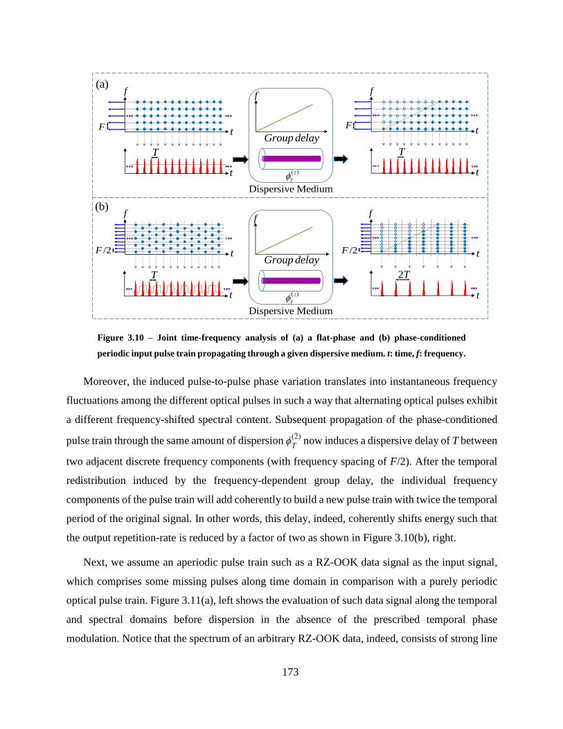
173
Group delay
t
Dispersive Medium
(a)
(b)
2
T
T
F
f
t
t
t
t
t
t
t
f
f f
T
F
/2F /2F
f
f
Group delay
Dispersive Medium
2
T
T 2T
Figure 3.10 – Joint time-frequency analysis of (a) a flat-phase and (b) phase-conditioned
periodic input pulse train propagating through a given dispersive medium. t: time, f: frequency.
Moreover, the induced pulse-to-pulse phase variation translates into instantaneous frequency
fluctuations among the different optical pulses in such a way that alternating optical pulses exhibit
a different frequency-shifted spectral content. Subsequent propagation of the phase-conditioned
pulse train through the same amount of dispersion ϕT
(2) now induces a dispersive delay of T between
two adjacent discrete frequency components (with frequency spacing of F/2). After the temporal
redistribution induced by the frequency-dependent group delay, the individual frequency
components of the pulse train will add coherently to build a new pulse train with twice the temporal
period of the original signal. In other words, this delay, indeed, coherently shifts energy such that
the output repetition-rate is reduced by a factor of two as shown in Figure 3.10(b), right.
Next, we assume an aperiodic pulse train such as a RZ-OOK data signal as the input signal,
which comprises some missing pulses along time domain in comparison with a purely periodic
optical pulse train. Figure 3.11(a), left shows the evaluation of such data signal along the temporal
and spectral domains before dispersion in the absence of the prescribed temporal phase
modulation. Notice that the spectrum of an arbitrary RZ-OOK data, indeed, consists of strong line
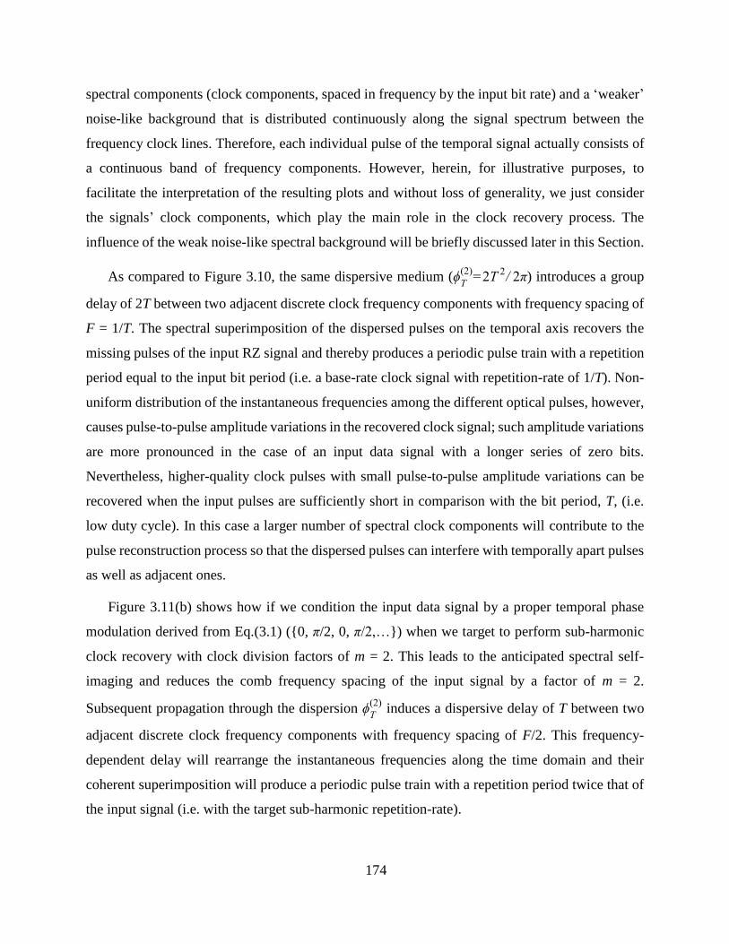
174
spectral components (clock components, spaced in frequency by the input bit rate) and a ‘weaker’
noise-like background that is distributed continuously along the signal spectrum between the
frequency clock lines. Therefore, each individual pulse of the temporal signal actually consists of
a continuous band of frequency components. However, herein, for illustrative purposes, to
facilitate the interpretation of the resulting plots and without loss of generality, we just consider
the signals’ clock components, which play the main role in the clock recovery process. The
influence of the weak noise-like spectral background will be briefly discussed later in this Section.
As compared to Figure 3.10, the same dispersive medium (ϕT
(2)=2T 2/ 2π) introduces a group
delay of 2T between two adjacent discrete clock frequency components with frequency spacing of
F = 1/T. The spectral superimposition of the dispersed pulses on the temporal axis recovers the
missing pulses of the input RZ signal and thereby produces a periodic pulse train with a repetition
period equal to the input bit period (i.e. a base-rate clock signal with repetition-rate of 1/T). Non-
uniform distribution of the instantaneous frequencies among the different optical pulses, however,
causes pulse-to-pulse amplitude variations in the recovered clock signal; such amplitude variations
are more pronounced in the case of an input data signal with a longer series of zero bits.
Nevertheless, higher-quality clock pulses with small pulse-to-pulse amplitude variations can be
recovered when the input pulses are sufficiently short in comparison with the bit period, T, (i.e.
low duty cycle). In this case a larger number of spectral clock components will contribute to the
pulse reconstruction process so that the dispersed pulses can interfere with temporally apart pulses
as well as adjacent ones.
Figure 3.11(b) shows how if we condition the input data signal by a proper temporal phase
modulation derived from Eq.(3.1) ({0, π/2, 0, π/2,…}) when we target to perform sub-harmonic
clock recovery with clock division factors of m = 2. This leads to the anticipated spectral self-
imaging and reduces the comb frequency spacing of the input signal by a factor of m = 2.
Subsequent propagation through the dispersion ϕT
(2) induces a dispersive delay of T between two
adjacent discrete clock frequency components with frequency spacing of F/2. This frequency-
dependent delay will rearrange the instantaneous frequencies along the time domain and their
coherent superimposition will produce a periodic pulse train with a repetition period twice that of
the input signal (i.e. with the target sub-harmonic repetition-rate).
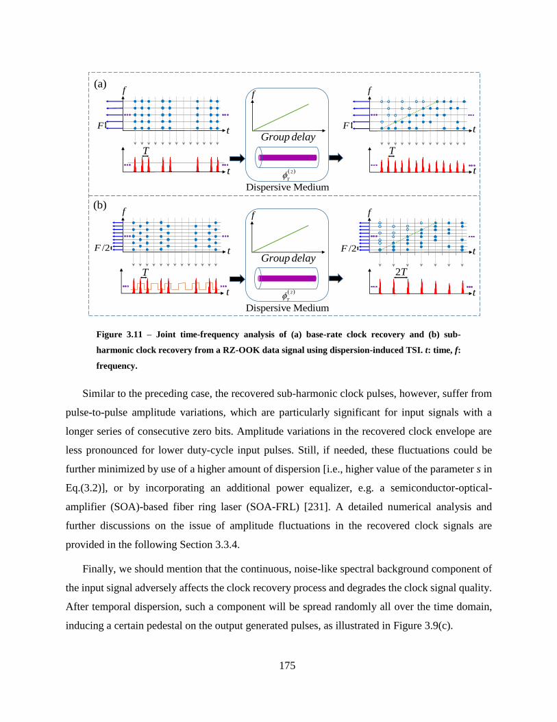
175
(a)
(b)
Group delay
t
Dispersive Medium
2
T
T
F
f
t
t
t
t
t
t
t
f
f f
T
F
/2F /2F
f
f
Group delay
Dispersive Medium
2
T
T 2T
Figure 3.11 – Joint time-frequency analysis of (a) base-rate clock recovery and (b) sub-
harmonic clock recovery from a RZ-OOK data signal using dispersion-induced TSI. t: time, f:
frequency.
Similar to the preceding case, the recovered sub-harmonic clock pulses, however, suffer from
pulse-to-pulse amplitude variations, which are particularly significant for input signals with a
longer series of consecutive zero bits. Amplitude variations in the recovered clock envelope are
less pronounced for lower duty-cycle input pulses. Still, if needed, these fluctuations could be
further minimized by use of a higher amount of dispersion [i.e., higher value of the parameter s in
Eq.(3.2)], or by incorporating an additional power equalizer, e.g. a semiconductor-optical-
amplifier (SOA)-based fiber ring laser (SOA-FRL) [231]. A detailed numerical analysis and
further discussions on the issue of amplitude fluctuations in the recovered clock signals are
provided in the following Section 3.3.4.
Finally, we should mention that the continuous, noise-like spectral background component of
the input signal adversely affects the clock recovery process and degrades the clock signal quality.
After temporal dispersion, such a component will be spread randomly all over the time domain,
inducing a certain pedestal on the output generated pulses, as illustrated in Figure 3.9(c).
176
3.3.4 Experimental demonstration and discussion
We next report on a proof-of-concept experiment to validate the proposed concept by
performing SHCR with clock division factors of m = 2, m = 3 and m =4, as well as BRCR from a
9.7Gbit/s data signal. Notice that, any desired repetition-rate division factor can be essentially
obtained in practice by appropriate control of the temporal phase modulation and dispersion-
induced spectral phase filtering. Nevertheless, to obtain higher SHCR orders, higher dispersion
values are required to realize the desired spectral phase filter. In this experiment, the highest
repetition-rate division factor (m = 4) was practically limited by the available dispersive medium
in our laboratories.
9.7 Gb/s Transmitter Sub-Harmonic Clock Recovery
9.7 GHz@1550
MLFL
AWG
Output
t
f f
MZMPC
PMPC
TODL
DCF
f
79.7 Gb/s
2 -1 PRBS
t
t
F F/2
F/2
RF AmpRF Amp
TT
2T
Figure 3.12 – Experimental setup of the sub-harmonic clock recovery technique through
dispersion-induced temporal self-imaging. MLFL: Mode-Locked Fiber Laser, MZM: Mach-
Zehnder Modulator, PC: Polarization Controller, AWG: Arbitrary Waveform Generator,
DCF: Dispersion-Compensating Fiber, PM: Phase Modulator, TODL: Tunable Optical Delay
Line, RF Amp: Radio-Frequency Amplifier, t: time, f: frequency.
The experimental setup used in our demonstration is sketched in Figure 3.12. The RZ-OOK
data signal is produced by intensity modulation of ~4 ps (intensity FWHM) optical pulses
generated by a mode-locked laser with a 9.7GHz repetition-rate at a central wavelength of 1550nm.
The modulator driver is a 27-1 pseudo-random bit sequence (PRBS), thus generating a RZ-OOK
modulated signal. The generated data signal is then delivered to the clock recovery circuit,
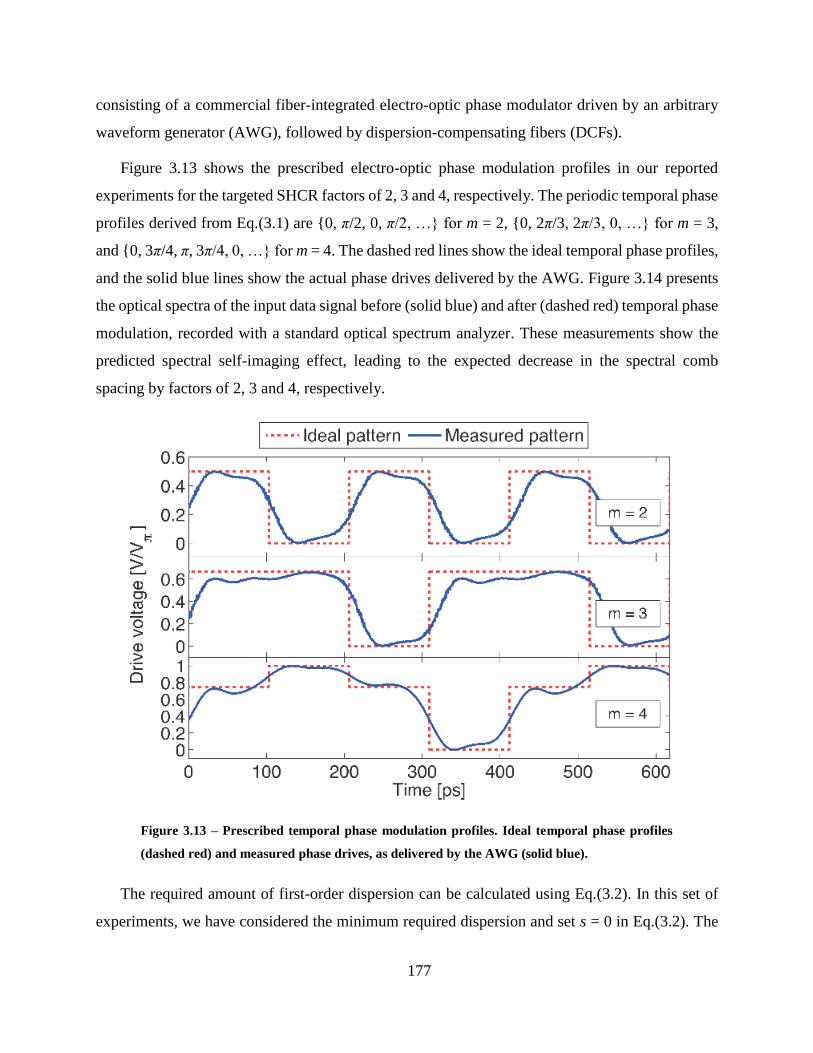
177
consisting of a commercial fiber-integrated electro-optic phase modulator driven by an arbitrary
waveform generator (AWG), followed by dispersion-compensating fibers (DCFs).
Figure 3.13 shows the prescribed electro-optic phase modulation profiles in our reported
experiments for the targeted SHCR factors of 2, 3 and 4, respectively. The periodic temporal phase
profiles derived from Eq.(3.1) are {0, π/2, 0, π/2, …} for m = 2, {0, 2π/3, 2π/3, 0, …} for m = 3,
and {0, 3π/4, π, 3π/4, 0, …} for m = 4. The dashed red lines show the ideal temporal phase profiles,
and the solid blue lines show the actual phase drives delivered by the AWG. Figure 3.14 presents
the optical spectra of the input data signal before (solid blue) and after (dashed red) temporal phase
modulation, recorded with a standard optical spectrum analyzer. These measurements show the
predicted spectral self-imaging effect, leading to the expected decrease in the spectral comb
spacing by factors of 2, 3 and 4, respectively.
Figure 3.13 – Prescribed temporal phase modulation profiles. Ideal temporal phase profiles
(dashed red) and measured phase drives, as delivered by the AWG (solid blue).
The required amount of first-order dispersion can be calculated using Eq.(3.2). In this set of
experiments, we have considered the minimum required dispersion and set s = 0 in Eq.(3.2). The
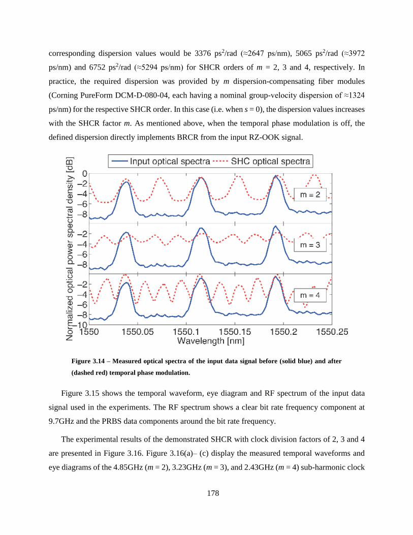
178
corresponding dispersion values would be 3376 ps2/rad (≈2647 ps/nm), 5065 ps2/rad (≈3972
ps/nm) and 6752 ps2/rad (≈5294 ps/nm) for SHCR orders of m = 2, 3 and 4, respectively. In
practice, the required dispersion was provided by m dispersion-compensating fiber modules
(Corning PureForm DCM-D-080-04, each having a nominal group-velocity dispersion of ≈1324
ps/nm) for the respective SHCR order. In this case (i.e. when s = 0), the dispersion values increases
with the SHCR factor m. As mentioned above, when the temporal phase modulation is off, the
defined dispersion directly implements BRCR from the input RZ-OOK signal.
Figure 3.14 – Measured optical spectra of the input data signal before (solid blue) and after
(dashed red) temporal phase modulation.
Figure 3.15 shows the temporal waveform, eye diagram and RF spectrum of the input data
signal used in the experiments. The RF spectrum shows a clear bit rate frequency component at
9.7GHz and the PRBS data components around the bit rate frequency.
The experimental results of the demonstrated SHCR with clock division factors of 2, 3 and 4
are presented in Figure 3.16. Figure 3.16(a)– (c) display the measured temporal waveforms and
eye diagrams of the 4.85GHz (m = 2), 3.23GHz (m = 3), and 2.43GHz (m = 4) sub-harmonic clock
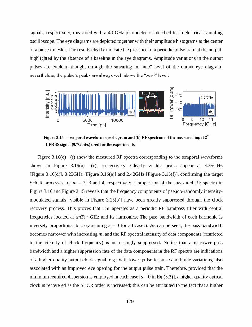
179
signals, respectively, measured with a 40-GHz photodetector attached to an electrical sampling
oscilloscope. The eye diagrams are depicted together with their amplitude histograms at the center
of a pulse timeslot. The results clearly indicate the presence of a periodic pulse train at the output,
highlighted by the absence of a baseline in the eye diagrams. Amplitude variations in the output
pulses are evident, though, through the smearing in “one” level of the output eye diagram;
nevertheless, the pulse’s peaks are always well above the “zero” level.
Figure 3.15 – Temporal waveform, eye diagram and (b) RF spectrum of the measured input 27
–1 PRBS signal (9.7Gbit/s) used for the experiments.
Figure 3.16(d)– (f) show the measured RF spectra corresponding to the temporal waveforms
shown in Figure 3.16(a)– (c), respectively. Clearly visible peaks appear at 4.85GHz
[Figure 3.16(d)], 3.23GHz [Figure 3.16(e)] and 2.42GHz [Figure 3.16(f)], confirming the target
SHCR processes for m = 2, 3 and 4, respectively. Comparison of the measured RF spectra in
Figure 3.16 and Figure 3.15 reveals that the frequency components of pseudo-randomly intensity-
modulated signals [visible in Figure 3.15(b)] have been greatly suppressed through the clock
recovery process. This proves that TSI operates as a periodic RF bandpass filter with central
frequencies located at (mT)-1 GHz and its harmonics. The pass bandwidth of each harmonic is
inversely proportional to m (assuming s = 0 for all cases). As can be seen, the pass bandwidth
becomes narrower with increasing m, and the RF spectral intensity of data components (restricted
to the vicinity of clock frequency) is increasingly suppressed. Notice that a narrower pass
bandwidth and a higher suppression rate of the data components in the RF spectra are indications
of a higher-quality output clock signal, e.g., with lower pulse-to-pulse amplitude variations, also
associated with an improved eye opening for the output pulse train. Therefore, provided that the
minimum required dispersion is employed in each case [s = 0 in Eq.(3.2)], a higher quality optical
clock is recovered as the SHCR order is increased; this can be attributed to the fact that a higher
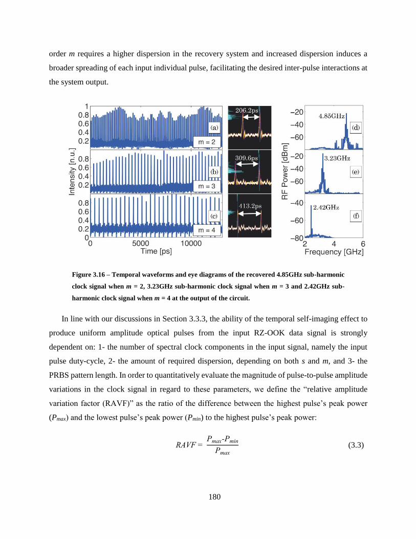
180
order m requires a higher dispersion in the recovery system and increased dispersion induces a
broader spreading of each input individual pulse, facilitating the desired inter-pulse interactions at
the system output.
Figure 3.16 – Temporal waveforms and eye diagrams of the recovered 4.85GHz sub-harmonic
clock signal when m = 2, 3.23GHz sub-harmonic clock signal when m = 3 and 2.42GHz sub-
harmonic clock signal when m = 4 at the output of the circuit.
In line with our discussions in Section 3.3.3, the ability of the temporal self-imaging effect to
produce uniform amplitude optical pulses from the input RZ-OOK data signal is strongly
dependent on: 1- the number of spectral clock components in the input signal, namely the input
pulse duty-cycle, 2- the amount of required dispersion, depending on both s and m, and 3- the
PRBS pattern length. In order to quantitatively evaluate the magnitude of pulse-to-pulse amplitude
variations in the clock signal in regard to these parameters, we define the “relative amplitude
variation factor (RAVF)” as the ratio of the difference between the highest pulse’s peak power
(Pmax) and the lowest pulse’s peak power (Pmin) to the highest pulse’s peak power:
RAVF = Pmax-Pmin
Pmax
(3.3)
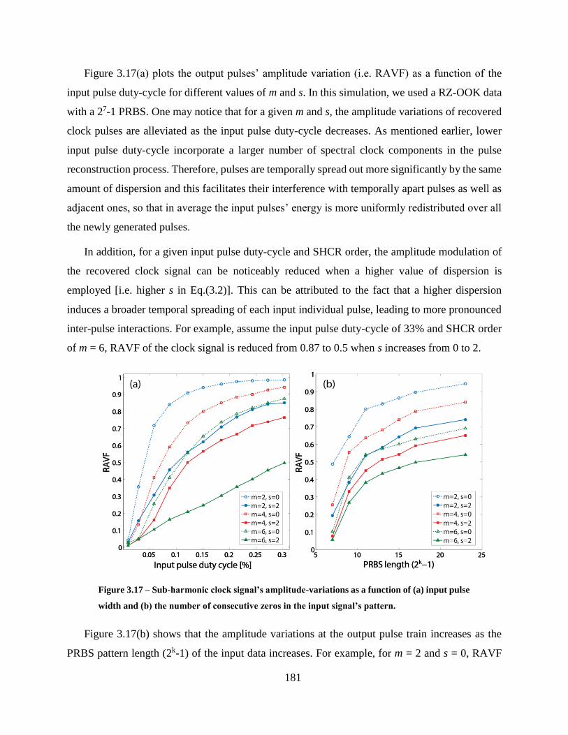
181
Figure 3.17(a) plots the output pulses’ amplitude variation (i.e. RAVF) as a function of the
input pulse duty-cycle for different values of m and s. In this simulation, we used a RZ-OOK data
with a 27-1 PRBS. One may notice that for a given m and s, the amplitude variations of recovered
clock pulses are alleviated as the input pulse duty-cycle decreases. As mentioned earlier, lower
input pulse duty-cycle incorporate a larger number of spectral clock components in the pulse
reconstruction process. Therefore, pulses are temporally spread out more significantly by the same
amount of dispersion and this facilitates their interference with temporally apart pulses as well as
adjacent ones, so that in average the input pulses’ energy is more uniformly redistributed over all
the newly generated pulses.
In addition, for a given input pulse duty-cycle and SHCR order, the amplitude modulation of
the recovered clock signal can be noticeably reduced when a higher value of dispersion is
employed [i.e. higher s in Eq.(3.2)]. This can be attributed to the fact that a higher dispersion
induces a broader temporal spreading of each input individual pulse, leading to more pronounced
inter-pulse interactions. For example, assume the input pulse duty-cycle of 33% and SHCR order
of m = 6, RAVF of the clock signal is reduced from 0.87 to 0.5 when s increases from 0 to 2.
Figure 3.17 – Sub-harmonic clock signal’s amplitude-variations as a function of (a) input pulse
width and (b) the number of consecutive zeros in the input signal’s pattern.
Figure 3.17(b) shows that the amplitude variations at the output pulse train increases as the
PRBS pattern length (2k-1) of the input data increases. For example, for m = 2 and s = 0, RAVF
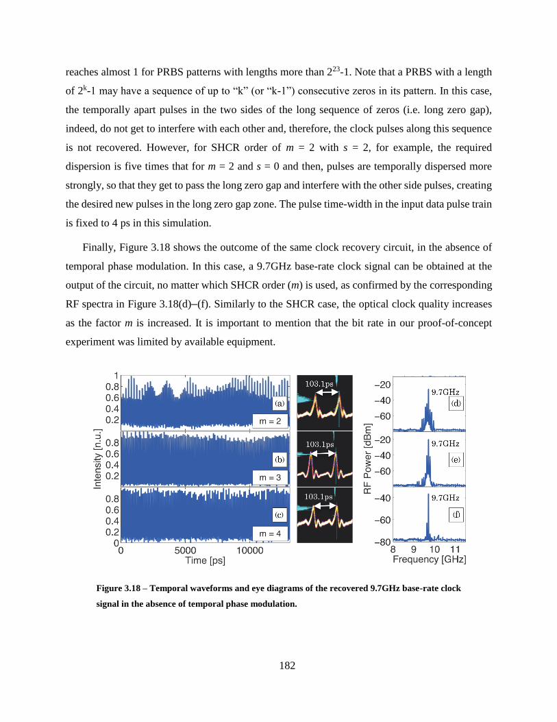
182
reaches almost 1 for PRBS patterns with lengths more than 223-1. Note that a PRBS with a length
of 2k-1 may have a sequence of up to “k” (or “k-1”) consecutive zeros in its pattern. In this case,
the temporally apart pulses in the two sides of the long sequence of zeros (i.e. long zero gap),
indeed, do not get to interfere with each other and, therefore, the clock pulses along this sequence
is not recovered. However, for SHCR order of m = 2 with s = 2, for example, the required
dispersion is five times that for m = 2 and s = 0 and then, pulses are temporally dispersed more
strongly, so that they get to pass the long zero gap and interfere with the other side pulses, creating
the desired new pulses in the long zero gap zone. The pulse time-width in the input data pulse train
is fixed to 4 ps in this simulation.
Finally, Figure 3.18 shows the outcome of the same clock recovery circuit, in the absence of
temporal phase modulation. In this case, a 9.7GHz base-rate clock signal can be obtained at the
output of the circuit, no matter which SHCR order (m) is used, as confirmed by the corresponding
RF spectra in Figure 3.18(d)–(f). Similarly to the SHCR case, the optical clock quality increases
as the factor m is increased. It is important to mention that the bit rate in our proof-of-concept
experiment was limited by available equipment.
Figure 3.18 – Temporal waveforms and eye diagrams of the recovered 9.7GHz base-rate clock
signal in the absence of temporal phase modulation.
183
It is well known that TSI is more easily observable as the pulse bit rate is increased since a
lower dispersion amount is then required. Moreover, alternatively, the quadratic time phase
modulation can be applied using non-linear optical processes, e.g. cross-phase-modulation with a
parabolic pump pulse train, overcoming the intrinsic speed limitations of electro-optic phase
modulation [232].
3.3.5 Conclusions
In summary, the effect of inverse temporal self-imaging (I-TSI) on aperiodic pulse trains have
been investigated and studied. Results on this study suggest a novel scheme for reconfigurable
sub-harmonic optical clock recovery based on I-TSI, involving phase-only temporal modulation
and dispersive spectral filtering of the input data pulse train. The scheme can be easily reconfigured
to achieve base-rate clock recovery by simply bypassing the temporal phase-modulation step. The
proposed scheme has been validated through experimental demonstrations, and in particular, we
have reported successful extraction of 4.85-GHz and 3.23-GHz sub-harmonic clock signals as well
as the 9.7-GHz base-rate clock signal from a 9.7-Gbit/s RZ-OOK data signal under a 27-1 PRBS
pattern. The quality of the recovered optical clock signal is improved for a higher sub-harmonic
rate factor, a higher dispersion amount for temporal self-imaging [higher ‘s’ in Eq. (2)], or lower
duty-cycle input pulses.
184
3.4 640 Gbit/s return-to-zero to non-return-to-zero format
conversion based on optical linear spectral phase filtering23
3.4.1 Abstract
We propose a novel approach for all-optical return-to-zero (RZ)-to-non-RZ (NRZ)
telecommunication data format conversion based on linear spectral phase manipulation of an RZ
data signal. The operation principle is numerically analyzed and experimentally validated through
successful format conversion of a 640 Gbit/s coherent RZ signal into the equivalent NRZ time-
domain data using a simple phase filter implemented by a commercial optical wave-shaper.
3.4.2 Introduction
Future optical networks are likely a hybrid scenario of various technologies owing to the large
variety of applications and to their hierarchical structure, which implies diverse specifications for
the networks’ segments. In this context, a specific network segment employs an adequate
modulation format that meets its requirements [102, 103]. Therefore, all-optical format converters
are of great importance to transparently and seamlessly interconnect different parts of the
networks, avoiding the use of optical-to-electrical (O/E) and electrical-to-optical (E/O) converters,
as well as overcoming limitations imposed by electronics in terms of bit rate and frequency
bandwidth [103]. In particular, format conversion between RZ and NRZ signals is particularly
interesting: both formats are mature and widely used in different parts of the networks, e.g., the
RZ format is adopted in time division-multiplexing (OTDM) systems to be able to perform pulse
multiplexing, while the NRZ format is preferred in wavelength-division-multiplexing (WDM)
systems due to its higher spectral efficiency [71]. In addition, format conversion of an RZ signal
to its equivalent NRZ is also desired in de-multiplexing of OTDM signals as NRZ signals improve
timing-jitter tolerance in the de-multiplexing process thanks to their flat-top temporal shape [104].
23 R. Maram, D. Kong, M. Galili, L. K. Oxenløwe and J. Azaña, “640 Gbit/s return-to-zero to non-return-to-zero
format conversion based on optical linear spectral phase filtering,” Optics Letters, vol. 41, no. 1, pp. 64-67 (2016).
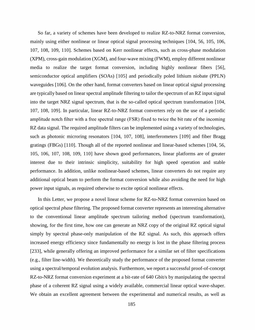
185
So far, a variety of schemes have been developed to realize RZ-to-NRZ format conversion,
mainly using either nonlinear or linear optical signal processing techniques [104, 56, 105, 106,
107, 108, 109, 110]. Schemes based on Kerr nonlinear effects, such as cross-phase modulation
(XPM), cross-gain modulation (XGM), and four-wave mixing (FWM), employ different nonlinear
media to realize the target format conversion, including highly nonlinear fibers [56],
semiconductor optical amplifiers (SOAs) [105] and periodically poled lithium niobate (PPLN)
waveguides [106]. On the other hand, format converters based on linear optical signal processing
are typically based on linear spectral amplitude filtering to tailor the spectrum of an RZ input signal
into the target NRZ signal spectrum, that is the so-called optical spectrum transformation [104,
107, 108, 109]. In particular, linear RZ-to-NRZ format converters rely on the use of a periodic
amplitude notch filter with a free spectral range (FSR) fixed to twice the bit rate of the incoming
RZ data signal. The required amplitude filters can be implemented using a variety of technologies,
such as photonic microring resonators [104, 107, 108], interferometers [109] and fiber Bragg
gratings (FBGs) [110]. Though all of the reported nonlinear and linear-based schemes [104, 56,
105, 106, 107, 108, 109, 110] have shown good performances, linear platforms are of greater
interest due to their intrinsic simplicity, suitability for high speed operation and stable
performance. In addition, unlike nonlinear-based schemes, linear converters do not require any
additional optical beam to perform the format conversion while also avoiding the need for high
power input signals, as required otherwise to excite optical nonlinear effects.
In this Letter, we propose a novel linear scheme for RZ-to-NRZ format conversion based on
optical spectral phase filtering. The proposed format converter represents an interesting alternative
to the conventional linear amplitude spectrum tailoring method (spectrum transformation),
showing, for the first time, how one can generate an NRZ copy of the original RZ optical signal
simply by spectral phase-only manipulation of the RZ signal. As such, this approach offers
increased energy efficiency since fundamentally no energy is lost in the phase filtering process
[233], while generally offering an improved performance for a similar set of filter specifications
(e.g., filter line-width). We theoretically study the performance of the proposed format converter
using a spectral/temporal evolution analysis. Furthermore, we report a successful proof-of-concept
RZ-to-NRZ format conversion experiment at a bit-rate of 640 Gbit/s by manipulating the spectral
phase of a coherent RZ signal using a widely available, commercial linear optical wave-shaper.
We obtain an excellent agreement between the experimental and numerical results, as well as
186
provide preliminary bit-error-rate (BER) measurements, validating the performance of the newly
proposed format-conversion concept.
3.4.3 Operation principle and simulation results
Optical spectrum transformation method [104, 107, 108, 109] relies on the suppression of the
first-order harmonic components in the spectrum of an RZ signal using a periodic amplitude notch
filter whose FSR is matched to twice the signal bit rate. The resulting converted NRZ signal after
the notch filter yet exhibits relatively large amplitude ripples due to the residual high-frequency
components of the spectrum [104, 109]. Therefore, a narrow optical band-pass filter (OBPF) is
typically used to eliminate these residual components, leading to a reduction of the amplitude
ripples and the associated improvement in the quality of the converted NRZ signal.
Herein, we show that a properly designed optical phase filter can also perform the RZ-to-NRZ
format conversion by simply phase-shifting the first-order harmonic components in the spectrum
of the RZ signal, instead of entirely suppressing them.
The operation principle of the proposed approach is shown in Figure 3.19(a)-(f). To analyze
the principle of format conversion, we study progressively the evolution of the RZ signal in the
frequency domain and time domain through numerical simulations based on the standard
frequency-domain method for linear processes. By definition, the Fourier transform of the input
signal is multiplied by the frequency-domain transfer function of the linear filters under test, and
the output is inverse-Fourier-transformed to produce the time-domain signal. Figure 3.19(a)–(c)
show evolution of the relevant spectra, while Figure 3.19(d)–(f) are the corresponding time-
domain eye diagrams.
Figure 3.19(a) and (d) show the spectrum and eye diagram of a RZ data signal consisting of
700-fs (FWHM) optical pulses at a bit rate of 640 Gbit/s, coded under a pseudorandom bit
sequence (PRBS) of 27 – 1. In Figure 3.19(a), the red curve shows the spectral phase of the used
phase filter with a spectral line-width of Fb =10 GHz and a free spectral range (FSR) of 1,280
GHz, which is twice the input signal bit rate. The phase filter π-phase-shifts the first-order
harmonic components of the RZ signal with respect to the rest of the signal spectrum.
187
Po
wer
(d
Bm
) P
ow
er (
dB
m)/
T(d
B)
Po
wer
(d
Bm
)
Po
wer (a.u
.)P
ow
er (a.u.)
Time (ps)
Po
wer (a.u
.)
Ph
ase (Rad
)
-80
-60
-40
-20
0
-1000 -500 0 500 1000
(b) OBPF
-80
-60
-40
-20
0
-1000 -500 0 500 1000
Frequency (GHz)
(c)
0 1 2 3
0
0.2
0.4
0.6
0.8
1(f)
0
4(a)
-80
-60
-40
-20
0
-1000 -500 0 500 1000
PF
0 1 2 3
0
0.2
0.4
0.6
0.8
1(d)
0 1 2 3
0
0.2
0.4
0.6
0.8
1(e)
Figure 3.19 – Numerical simulation results. (a)-(f): spectra and eye diagrams evolution of the
proposed method for format conversion from RZ to NRZ at 640 Gbit/s. (a) and (d) are the
spectrum and eye diagram of the input RZ signal, respectively. (b) and (e) are the spectrum
and eye diagram of the RZ signal filtered by a suitable phase filter (PF), respectively. (c) and
(f) are the spectrum and eye diagram of the converted NRZ signal, after filtering by an OBPF,
respectively.
In Figure 3.19(b), the solid blue curve shows the spectrum of the RZ signal after phase filtering
– the filtered spectrum remains unchanged with respect to that of the input signal as the phase-
only filtering process does not alter the energy spectrum shape. However, the time-domain eye
diagram (shown in Figure 3.19(e)) reveals realization of the target format conversion from RZ to
NRZ. It is worth mentioning that the amplitude ripples of the converted NRZ signal after the phase
filter are significantly lower than those obtained using the amplitude notch filter approach in
188
previous reports [104, 109]. The quality of the converted NRZ signal can be further enhanced by
an additional OBPF to remove spectral components associated to the fast temporal features of the
signal that can be observed in the base-line of the eye diagram shown in Figure 3.19(e). The 3-dB
bandwidth of the OBPF used in this example, which is modeled as a Gaussian type filter, is
800GHz, as depicted in Figure 3.19(b). Figure 3.19(c) and (f) show the spectrum and eye diagram
of the converted NRZ signal, respectively, after filtering by the OBPF, confirming a clear quality
enhancement of the NRZ signal. It is noteworthy that the defined phase filter can be practically
implemented using a variety of technologies, such as line-by-line optical pulse shapers (e.g., the
wave shaper used in the experiments reported here), Fiber Bragg Gratings (FBG), thin film filters,
photonic ring resonators, and photonic crystals, among others [222, 223].
For a good format conversion, both a high Q-factor (defined as Q = (P1-P0) / (σ1+σ0), where
P1 and P0 are the means and σ1 and σ0 denote the standard deviations of the logic “one” and “zero”
levels, respectively) and low amplitude ripples (defined as the peak-to-peak power deviation of
the high level (logic “one” level) rail in the converted NRZ normalized eye diagram) are
simultaneously required for the converted NRZ signal [71]. Figure 3.20(a) and (b) show the
simulated Q-factor and amplitude ripples of the converted NRZ signal as a function of spectral
line-width of the phase filter and the OBPF 3-dB bandwidth at a bit-rate of 640 Gbit/s.
One can find optimal regions for bandwidth of the OBPF and spectral line-width of the phase
filter, which are denoted by the ellipses in Figure 3.20(a) and (b). A phase filter with a line-width
Fb narrower than ~10 GHz and an OBPF with a bandwidth around 800 GHz will result in an
optimum RZ-to-NRZ format conversion performance, with high Q-factor and low amplitude
ripples. In the presented numerical example, shown in Fig. 1, the Q-factor and amplitude ripple of
the converted NRZ data signal are 27.7 and 0.073, respectively, for a phase filter spectral line-
width of 10GHz and an OBPF 3-dB bandwidth of 800GHz. Recall that these values are feasible
with present filter technologies. It is worth restating that the results presented in Figure 3.20 are
obtained for an input data signal with a PRBS length of 27 – 1 and a bit-rate of 640Gbit/s. By
changing the PRBS length and/or the bit-rate, the required filtering specifications will change
accordingly. In particular, by increasing the PRBS length and/or reducing the bit-rate, a narrower
line-width is required for the phase filter.
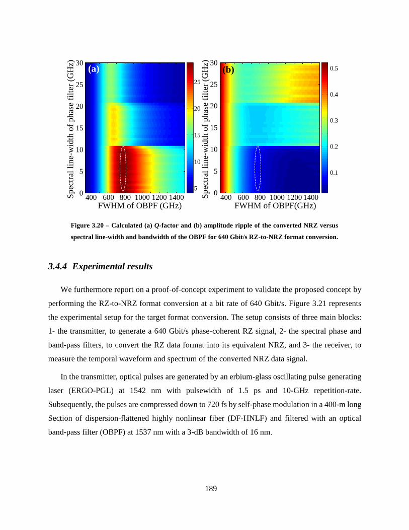
189
0
5
10
15
20
25
30
FWHM of OBPF (GHz)400 600 800 1000 1200 1400S
pec
tral
lin
e-w
idth
of
ph
ase
filt
er (
GH
z)
5
10
15
20
25
(a)
0.1
0.2
0.3
0.4
0.5
0
5
10
15
20
25
30
FWHM of OBPF(GHz)400 600 800 1000 1200 1400S
pec
tral
lin
e-w
idth
of
ph
ase
filt
er (
GH
z)
(b)
Figure 3.20 – Calculated (a) Q-factor and (b) amplitude ripple of the converted NRZ versus
spectral line-width and bandwidth of the OBPF for 640 Gbit/s RZ-to-NRZ format conversion.
3.4.4 Experimental results
We furthermore report on a proof-of-concept experiment to validate the proposed concept by
performing the RZ-to-NRZ format conversion at a bit rate of 640 Gbit/s. Figure 3.21 represents
the experimental setup for the target format conversion. The setup consists of three main blocks:
1- the transmitter, to generate a 640 Gbit/s phase-coherent RZ signal, 2- the spectral phase and
band-pass filters, to convert the RZ data format into its equivalent NRZ, and 3- the receiver, to
measure the temporal waveform and spectrum of the converted NRZ data signal.
In the transmitter, optical pulses are generated by an erbium-glass oscillating pulse generating
laser (ERGO-PGL) at 1542 nm with pulsewidth of 1.5 ps and 10-GHz repetition-rate.
Subsequently, the pulses are compressed down to 720 fs by self-phase modulation in a 400-m long
Section of dispersion-flattened highly nonlinear fiber (DF-HNLF) and filtered with an optical
band-pass filter (OBPF) at 1537 nm with a 3-dB bandwidth of 16 nm.
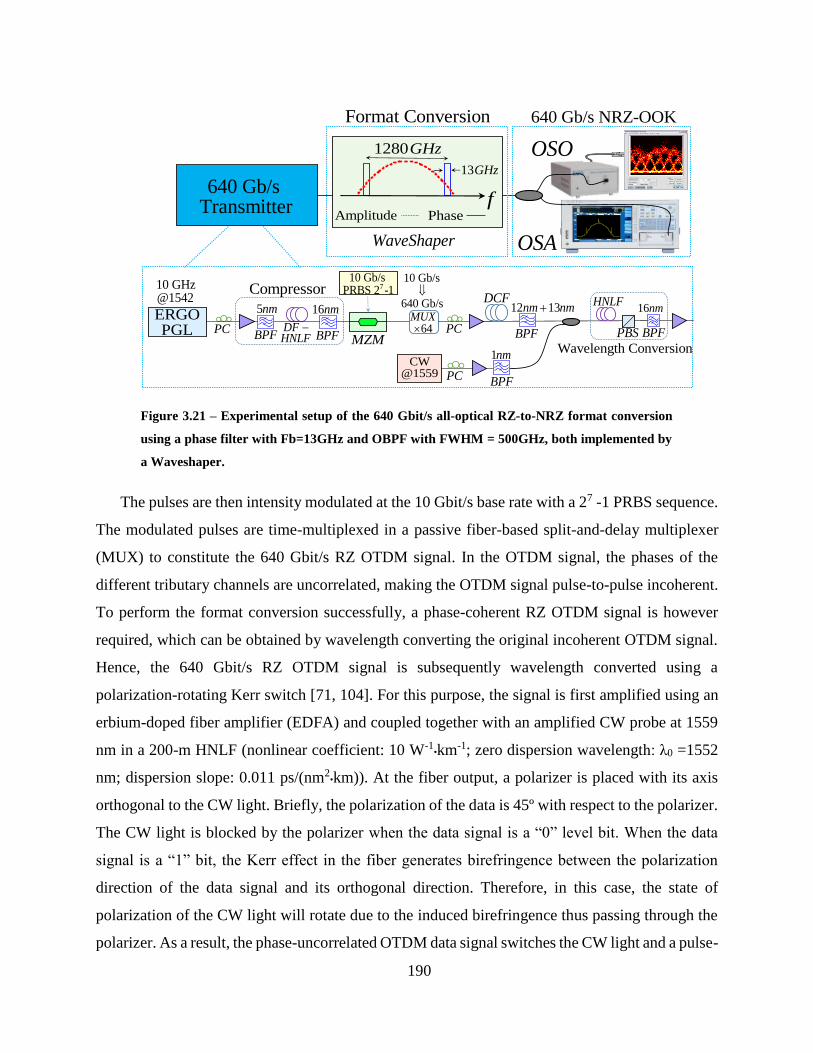
190
OSO
WaveShaper OSA
640 Gb/s Transmitter
ERGOPGL
10 GHz@1542
Compressor
5nm 16nm
BPFPC
710 Gb/s
PRBS 2 -110 Gb/s
640 Gb/s
DFHNLF
MZM
64MUX
CW@1559
Wavelength Conversion
DCF12 13nm nm
1nm
HNLF
PBS
16nm
f
1280GHz
Amplitude Phase
13GHz
Format Conversion 640 Gb/s NRZ-OOK
BPF BPF
BPF
BPFPC
PC
Figure 3.21 – Experimental setup of the 640 Gbit/s all-optical RZ-to-NRZ format conversion
using a phase filter with Fb=13GHz and OBPF with FWHM = 500GHz, both implemented by
a Waveshaper.
The pulses are then intensity modulated at the 10 Gbit/s base rate with a 27 -1 PRBS sequence.
The modulated pulses are time-multiplexed in a passive fiber-based split-and-delay multiplexer
(MUX) to constitute the 640 Gbit/s RZ OTDM signal. In the OTDM signal, the phases of the
different tributary channels are uncorrelated, making the OTDM signal pulse-to-pulse incoherent.
To perform the format conversion successfully, a phase-coherent RZ OTDM signal is however
required, which can be obtained by wavelength converting the original incoherent OTDM signal.
Hence, the 640 Gbit/s RZ OTDM signal is subsequently wavelength converted using a
polarization-rotating Kerr switch [71, 104]. For this purpose, the signal is first amplified using an
erbium-doped fiber amplifier (EDFA) and coupled together with an amplified CW probe at 1559
nm in a 200-m HNLF (nonlinear coefficient: 10 W-1•km-1; zero dispersion wavelength: λ0 =1552
nm; dispersion slope: 0.011 ps/(nm2•km)). At the fiber output, a polarizer is placed with its axis
orthogonal to the CW light. Briefly, the polarization of the data is 45º with respect to the polarizer.
The CW light is blocked by the polarizer when the data signal is a “0” level bit. When the data
signal is a “1” bit, the Kerr effect in the fiber generates birefringence between the polarization
direction of the data signal and its orthogonal direction. Therefore, in this case, the state of
polarization of the CW light will rotate due to the induced birefringence thus passing through the
polarizer. As a result, the phase-uncorrelated OTDM data signal switches the CW light and a pulse-
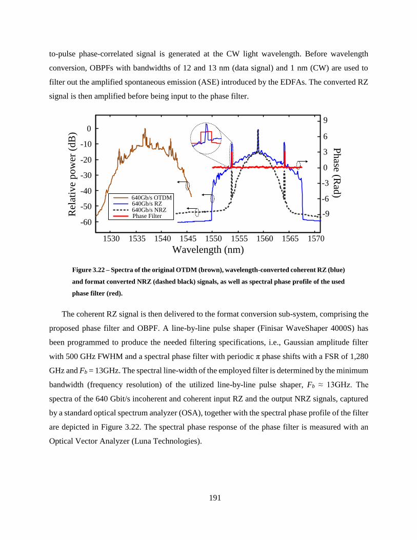
191
to-pulse phase-correlated signal is generated at the CW light wavelength. Before wavelength
conversion, OBPFs with bandwidths of 12 and 13 nm (data signal) and 1 nm (CW) are used to
filter out the amplified spontaneous emission (ASE) introduced by the EDFAs. The converted RZ
signal is then amplified before being input to the phase filter.
1530 1535 1540 1545 1550 1555 1560 1565 1570
-60
Rel
ativ
e pow
er (
dB
)
Wavelength (nm)
-50
-40
-30
-20
-10
0
-6
-3
0
3
6
-9
9
640Gb/s OTDM640Gb/s RZ
Phase Filter640Gb/s NRZ
Phase (R
ad)
Figure 3.22 – Spectra of the original OTDM (brown), wavelength-converted coherent RZ (blue)
and format converted NRZ (dashed black) signals, as well as spectral phase profile of the used
phase filter (red).
The coherent RZ signal is then delivered to the format conversion sub-system, comprising the
proposed phase filter and OBPF. A line-by-line pulse shaper (Finisar WaveShaper 4000S) has
been programmed to produce the needed filtering specifications, i.e., Gaussian amplitude filter
with 500 GHz FWHM and a spectral phase filter with periodic π phase shifts with a FSR of 1,280
GHz and Fb = 13GHz. The spectral line-width of the employed filter is determined by the minimum
bandwidth (frequency resolution) of the utilized line-by-line pulse shaper, Fb ≈ 13GHz. The
spectra of the 640 Gbit/s incoherent and coherent input RZ and the output NRZ signals, captured
by a standard optical spectrum analyzer (OSA), together with the spectral phase profile of the filter
are depicted in Figure 3.22. The spectral phase response of the phase filter is measured with an
Optical Vector Analyzer (Luna Technologies).
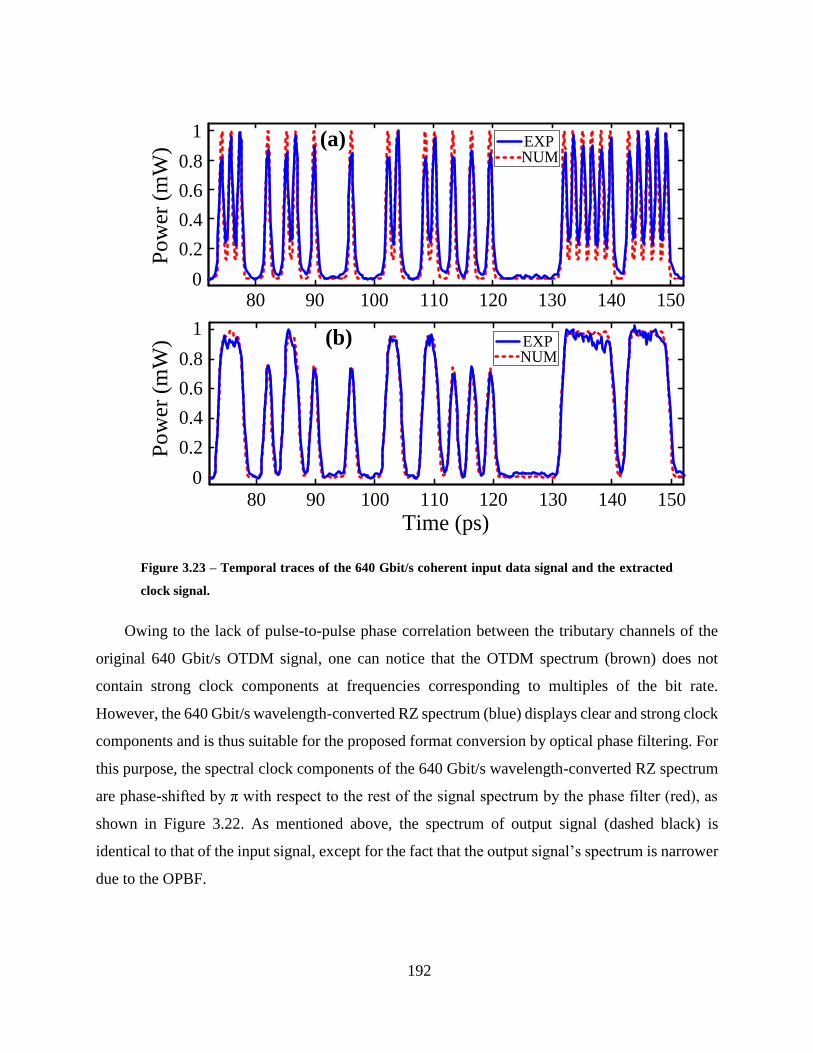
192
80 90 100 110 120 130 140 1500
0.2
0.4
0.6
0.8
1
Pow
er (
mW
)
Time (ps)
(a) EXPNUM
80 90 100 110 120 130 140 1500
0.2
0.4
0.6
0.8
1
Pow
er (
mW
) (b) EXPNUM
Figure 3.23 – Temporal traces of the 640 Gbit/s coherent input data signal and the extracted
clock signal.
Owing to the lack of pulse-to-pulse phase correlation between the tributary channels of the
original 640 Gbit/s OTDM signal, one can notice that the OTDM spectrum (brown) does not
contain strong clock components at frequencies corresponding to multiples of the bit rate.
However, the 640 Gbit/s wavelength-converted RZ spectrum (blue) displays clear and strong clock
components and is thus suitable for the proposed format conversion by optical phase filtering. For
this purpose, the spectral clock components of the 640 Gbit/s wavelength-converted RZ spectrum
are phase-shifted by π with respect to the rest of the signal spectrum by the phase filter (red), as
shown in Figure 3.22. As mentioned above, the spectrum of output signal (dashed black) is
identical to that of the input signal, except for the fact that the output signal’s spectrum is narrower
due to the OPBF.
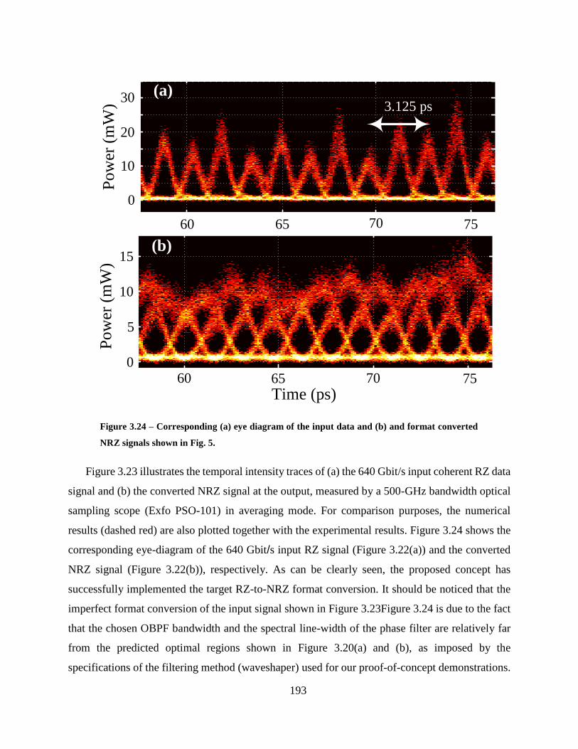
193
Time (ps)
Pow
er (
mW
)
60 70
15
10
5
0
65 75
(b)
Pow
er (
mW
)
60 70
30
20
10
0
65 75
(a)3.125 ps
Figure 3.24 – Corresponding (a) eye diagram of the input data and (b) and format converted
NRZ signals shown in Fig. 5.
Figure 3.23 illustrates the temporal intensity traces of (a) the 640 Gbit/s input coherent RZ data
signal and (b) the converted NRZ signal at the output, measured by a 500-GHz bandwidth optical
sampling scope (Exfo PSO-101) in averaging mode. For comparison purposes, the numerical
results (dashed red) are also plotted together with the experimental results. Figure 3.24 shows the
corresponding eye-diagram of the 640 Gbit/s input RZ signal (Figure 3.22(a)) and the converted
NRZ signal (Figure 3.22(b)), respectively. As can be clearly seen, the proposed concept has
successfully implemented the target RZ-to-NRZ format conversion. It should be noticed that the
imperfect format conversion of the input signal shown in Figure 3.23Figure 3.24 is due to the fact
that the chosen OBPF bandwidth and the spectral line-width of the phase filter are relatively far
from the predicted optimal regions shown in Figure 3.20(a) and (b), as imposed by the
specifications of the filtering method (waveshaper) used for our proof-of-concept demonstrations.
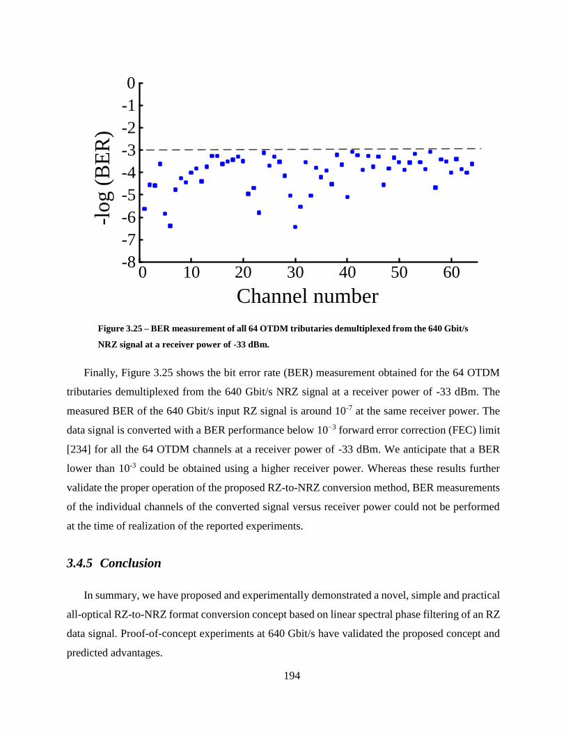
194
0 10 20 30 40 50 60-8
-7
-6
-5
-4
-3
-2
-1
0
Channel number
-log (
BE
R)
Figure 3.25 – BER measurement of all 64 OTDM tributaries demultiplexed from the 640 Gbit/s
NRZ signal at a receiver power of -33 dBm.
Finally, Figure 3.25 shows the bit error rate (BER) measurement obtained for the 64 OTDM
tributaries demultiplexed from the 640 Gbit/s NRZ signal at a receiver power of -33 dBm. The
measured BER of the 640 Gbit/s input RZ signal is around 10-7 at the same receiver power. The
data signal is converted with a BER performance below 10−3 forward error correction (FEC) limit
[234] for all the 64 OTDM channels at a receiver power of -33 dBm. We anticipate that a BER
lower than 10-3 could be obtained using a higher receiver power. Whereas these results further
validate the proper operation of the proposed RZ-to-NRZ conversion method, BER measurements
of the individual channels of the converted signal versus receiver power could not be performed
at the time of realization of the reported experiments.
3.4.5 Conclusion
In summary, we have proposed and experimentally demonstrated a novel, simple and practical
all-optical RZ-to-NRZ format conversion concept based on linear spectral phase filtering of an RZ
data signal. Proof-of-concept experiments at 640 Gbit/s have validated the proposed concept and
predicted advantages.

195

196
Chapter 4
4 Conclusions and Perspectives
4.1 Conclusions of the Thesis
Energy consumption is a key consideration in the development of practical circuits for optical
signal processing. From an energy consumption point of view, optical signal processing is
presently much more inefficient than electronic signal processing, which is a potentially significant
barrier to the practical use of optical circuits. Therefore, more attention needs to be paid to energy
consumption issues in the research and development of new optical technologies.
In this dissertation, we have directly addressed energy consumption issues by developing novel
signal-processing scheme to realize energy-efficient optical signal processors at high bit rates and
with energy consumption significantly lower than present optical counterparts. The demonstrated
schemes are based on the use of purely linear processes to manipulate the temporal and spectral
profiles of the signal under test, namely linear temporal modulation and/or linear spectral filtering,
respectively, to realize the target processing. The energy consumption is significantly reduced in
the desired functionalities due to the fact that the input signal energy can be fully preserved if only
the signal phase is manipulated in the time and spectral domains. In the newly proposed processors,
the incoming signal’s energy is effectively redistributed to build up the target output signal without
using any additional external optical power.
In Chapter 2, we use the combination of temporal and spectral Talbot effects, i.e., temporal
phase modulation and spectral phase filtering, to control and program the repetition rate of an input
pulse laser source. In particular, we have proposed a pulse repetition-rate multiplier that is simpler,
and far more flexible, and energy efficient than current approaches. For this proposed scheme, we
have provided a full analytical methodology to design and determine the system specifications. In
particular, we have derived an analytical equation for the temporal phase modulation profile that
197
is required to achieve a desired multiplication factor. The key feature of the proposed design is
that the dispersive medium is fixed and the multiplication factor can be programmed by simply
modifying the temporal phase modulation profile according to the derived formulation; the
repetition rate of the output signal can be tuned to be any integer multiple of the input repetition
rate. An experimental proof-of-concept has been successfully carried out by constructing a
programmable and stable fiber-optics source that can be tuned to operate at rates that are integer
multiples of ∼ 10GHz (input pulse repetition-rate) up to 40GHz. This all-fiber rate-multiplier can
be a simple and reliable source for fiber optics communications, optical computing, material
processing, frequency combs and nonlinear optics.
As the next step in Chapter 2, we have proposed and experimentally demonstrated, for the
first time to our knowledge, a lossless “fractional” pulse repetition-rate multiplication technique.
Using this proposed method, the output pulse train repetition rate can ideally be designed to be any
fractional multiple of the input repetition rate. This offers an unprecedented degree of flexibility
compared with previously reported PRRM approaches, which are generally limited to integer
repetition-rate multiplication factors. As an example, we experimentally demonstrated
multiplication factors of 1.25, 1.33, 1.5, 1.6, 1.75, 2.25, 2.33, and 2.5 with high fidelity from a
mode-locked laser with an input repetition rate between 10 and 20 GHz.
As the last step in Chapter 2, a new feature of the temporal Talbot effect, referred to as
“inverse” temporal Talbot effect, has been reported to demonstrate a passive amplification
technique for repetitive optical signals, where the energy of input repetitive pulses is coherently
accumulated to fewer replica pulses to build up an output signal with a reduced repetition rate and
intensity-amplified pulses. We have shown experimentally intensity amplification of repetitive
optical pulse waveforms with a gain from 2 to ~20, with the corresponding repetition-rate division.
This was, to my knowledge, the first report of a passive amplification method that does not amplify
or inject noise in the output signal and even enhances the extinction ratio and reduces noise
fluctuation of the input waveform train through its real-time averaging attribute. These noise-
mitigating effects allowed us to show in a side-by-side comparison in one of our experiments how
Talbot amplification can extract a weak noisy signal nearly buried beneath a noisy background,
whereas a typical active amplifier buries the signal further beneath the noise. Perhaps another,
greater significance of this work is how passive amplification using our method can be readily
198
applied to other spectral regions or wave systems, such as acoustic, electronic, and quantum. This
passive amplification technique is applicable to any wave system in which the temporal and
dispersive spectral phase can be controlled. Such control is not only available throughout the entire
electromagnetic spectrum, but also for many other wave systems, such as acoustic and matter
waves for which active gain mechanisms are extremely challenging to implement or simply not
available. For example, passive probability amplification of matter-waves could provide another
tool for atom optics to control and manipulate quantum states of matter as well as single photon
pulses.
In Chapter 3, we have developed novel approaches for base-rate and sub-harmonic clock
recovery of on-off-keying (OOK) data signals. In particular, the base-rate clock recovery technique
is based on spectral phase-only (all-pass) optical filtering. Besides its intrinsic implementation
simplicity, this technique significantly enhances both the recovered optical clock quality and
energy efficiency in comparison with conventional amplitude optical filtering approaches using a
Fabry–Perot filter. The proposed concept and predicted advantages were validated through
recovery of the optical clock from a 640 Gbit/s RZ-OOK data signal using a commercial linear
optical waveshaper. Furthermore, we proposed and experimentally demonstrated the realization
of a reconfigurable subharmonic clock recovery technique based on the inverse temporal Talbot
effect, involving temporal phase modulation and dispersive spectral filtering of the input data
signal. The scheme can be easily reconfigured to achieve base-rate clock recovery by simply
bypassing the temporal phase-modulation step. The proposed scheme has been validated through
experimental demonstrations, and in particular, we have reported successful extraction of 4.85-
GHz and 3.23-GHz sub-harmonic clock signals as well as the 9.7-GHz base-rate clock signal from
a 9.7-Gbit/s RZ-OOK data signal.
Finally, in Chapter 3, we have introduced a novel energy-efficient approach for all-optical
return-to-zero (RZ) to non-return-to-zero (NRZ) telecommunication data format conversion based
on linear spectral phase manipulation of an RZ data signal. The proposed format converter
represents an interesting alternative to the conventional linear amplitude spectrum tailoring method
(spectrum transformation), showing, for the first time, to my knowledge, how one can generate an
NRZ copy of the original RZ optical signal simply by spectral phase-only manipulation of the RZ
signal. The operation principle is numerically analyzed and experimentally validated through

199
successful format conversion of a 640 Gbit/s coherent RZ signal into the equivalent NRZ time-
domain data using a simple phase filter implemented by a commercial optical waveshaper. An
excellent agreement between the experimental and numerical results was achieved.
This research line to create energy-efficient optical functionalities may open new, important
perspectives for implementing other critical optical signal processors with unprecedented energy
efficiency, overcoming the energy-consumption limitations of present optical technologies without
trading their processing speed advantage.
4.2 Future perspectives
Next, we briefly discuss several potential lines of future research considered as of higher
relevance by the author:
1. In Chapter 1, we have proposed an implementation of a programmable fiber-optics pulse
repetition-rate multiplication approach. The dispersive medium is fixed to satisfy an integer Talbot
condition. However, in this approach, the maximum demonstrated multiplication factor is still
limited by two main problems. First, the needed amount of dispersion is generally very high, e.g.,
requiring the use of long fiber-optics dispersive lines, such that distortions induced by high-order
dispersion terms on picosecond-long pulses may not be negligible. Second, the ultimate
multiplication factor is additionally limited by the available electrical bandwidth of the arbitrary
waveform generator used to generate the multi-level phase modulation profile, which becomes
more complex (larger number of discrete phase levels) for higher multiplication factors. To
alleviate these problems, it should be possible to employ a more practical design using the
fractional Talbot condition for the dispersive medium. As such, this new design could be used to
electrically tune the repetition-rate of the output pulse train to higher multiplication factors with
lower amount of dispersion and a notably simpler phase modulation profile than that of the scheme
presented in this Thesis.
2. In Chapter 2, we used the combination of the temporal and spectral Talbot effect, i.e.,
temporal phase modulation and spectral phase filtering, to control and program the repetition-rate
of a low-rate laser source. We particularly derived specific formulations for the temporal phase
modulation profile and spectral filter to be able to generate uniform pulse trains at the output.
However, for many applications, including ultrahigh-speed optical communications and
200
photonically assisted generation of millimeter-wave and microwave electromagnetic waveforms,
it is desirable to generate high repetition-rate pulse trains with additional control on the amplitude
of each pulse. An extension of our work on programmable repetition-rate multiplication can be
investigated to design a programmable pulse repetition-rate multiplication with additional control
on the relative peak power of the output pulses. Using this envisioned scheme, the amplitude of
each single pulse in a period could be arbitrarily tailored by simply changing the temporal phase
modulation profile.
3. As mentioned in Chapter 2, one of the distinct characteristics of the Talbot-based passive
waveform amplification method is that it improves noise present on the input temporal signal,
effectively implementing a real-time averaging process. We have already demonstrated
experimentally this averaging effect for random (white) intensity noise (i.e. ASE-like noise). We
also predict that Talbot amplification can improve other important forms of noise, such as pulse-
to-pulse intensity fluctuation and timing-jitter, present on the input signal. A comprehensive
theoretical and experimental study needs to be conducted to examine these predictions.
4. The phase-only filtering technique used in Chapter 3 can also be applied for other crucial
signal processors, including logic gates. Logic gates are fundamental building blocks in digital
signal processing (DSP) circuits. In the last decade, a vast surge of research has been undertaken
to build optical logic gates. Though many optical logic gates have been demonstrated with speeds
thousands of times faster than the best electronics, the power required for most proposals is
approximately one thousand times higher than their electronic counterparts. As it is, the solutions
proposed for optical logic gates are much more inefficient from an energy consumption viewpoint
than current state-of-the-art electronics. General thermodynamic arguments show that
fundamentally, one should be able to design a logic gate that can consume arbitrarily low energy
(no lower limit), so-called “zero-energy” logic gates. In particular, several researchers recently
have proposed that a “zero-energy” gate could be designed with optics. In spite of many attempts,
the practical realization of a high-speed “zero energy” logic-gate has remained elusive. As an
extension of proposed optical functionalities proposed in this Thesis for processing optical data
signals, we envision the design and demonstration of zero-switching-energy logic gates using a
purely passive and phase-only linear process, a process that inherently preserves the entire input
signal energy, thus approaching the predicted “zero-energy” paradigm. The result of this follow-

201
up research may represent a new paradigm shift in gate design to implement optical logic with
significantly reduced energy consumption at ultrahigh speeds.
202
Chapitre 4
4 Conclusions ET Perspectives (en
français)
4.1 Conclusions de la Thèse
La consommation de l’énergie est un facteur clé dans le développement de circuits pratiques
pour le traitement du signal optique. En matière de consommation d’énergie, le traitement du
signal optique est actuellement beaucoup plus inefficace que le traitement de signal électronique,
qui est un obstacle important pour l’utilisation pratique des circuits optiques. Par conséquent, une
plus grande attention doit être accordée aux questions de consommation d’énergie dans la
recherche et le développement de nouvelles technologies optiques.
Dans cette thèse, nous avons abordé les problèmes de consommation d’énergie en développant
un nouveau système de traitement de signaux pour la réalisation des processeurs de signaux
optiques à haute efficacité énergétique travaillant à des débits élevés et avec une consommation
d’énergie nettement plus faible que celle des solutions optiques existantes actuellement. Ces
systèmes proposés sont basés sur l’utilisation de procédés purement linéaires pour manipuler les
profils temporels et spectraux du signal sous test, à savoir, la modulation temporelle linéaire et/ou
le filtrage spectral linéaire, respectivement, pour réaliser le traitement visé. La consommation
d’énergie est considérablement réduite dans les fonctionnalités souhaitées car l’énergie du signal
d’entrée peut être entièrement préservée si seule la phase du signal est manipulée dans les
domaines temporel et spectral. Dans les processeurs nouvellement proposés, l’énergie du signal
entrant est efficacement redistribuée pour construire le signal de sortie ciblé sans l’utilisation d’une
puissance optique externe supplémentaire.
203
Dans le Chapitre 2, nous avons utilisé la combinaison de l’effet Talbot temporel et spectral, à
savoir la modulation de phase temporelle et le filtrage de phase spectrale, pour contrôler et
programmer le taux de répétition et l’énergie par impulsion associée d’une source laser
impulsionnelle à faible taux de répétition. En particulier, nous avons proposé un multiplicateur de
taux de répétition d’impulsions qui est plus simple et beaucoup plus flexible et économe en énergie
que les approches actuelles. Pour ce système proposé, nous avons fourni une méthodologie
analytique complète pour concevoir et déterminer les exigences du système. En particulier, nous
avons établi une équation analytique pour le profil de modulation de phase temporelle requis pour
atteindre un facteur de multiplication souhaité. La principale caractéristique de la conception
proposée est que le milieu dispersif est fixé et le facteur de multiplication peut être programmé en
modifiant simplement le profil de la modulation de phase temporelle selon la formulation dérivée;
le taux de répétition du signal de sortie peut être réglé pour être un multiple entier quelconque du
taux répétition d’entrée. Une démonstration de faisabilité expérimentale a été réalisée avec succès
en construisant une source à fibre optique programmable et stable qui peut être réglé pour
fonctionner à des taux qui sont des multiples entiers de ~ 10GHz (taux de répétition d’entrée)
jusqu’à 40GHz. Ce multiplicateur de taux de répétition tout-fibre peut être une source simple et
fiable pour les communications par fibres optiques, l’informatique optique, le traitement des
matériaux, les peignes de fréquences et l’optique non linéaire.
Dans l’étape suivante dans le Chapitre 2, nous avons proposé et démontré expérimentalement,
pour la première fois à notre connaissance, une technique de multiplication sans perte et
fractionnaire du taux de répétition des impulsions. En utilisant cette méthode, le taux de répétition
du train d’impulsion de sortie peut être idéalement conçu pour être un multiple fractionnaire du
taux de répétition d’entrée, offrant un degré de flexibilité sans précédent par rapport aux approches
de multiplication rapportées précédemment, qui sont généralement limités à des facteurs de
multiplication entiers. A titre d’exemple, nous avons démontré expérimentalement des facteurs de
multiplication de 1,25, 1,33, 1,5, 1,6, 1,75, 2,25, 2,33 et 2,5 avec une haute fidélité à partir d’un
laser à verrouillage de mode et un taux de répétition d’entrée entre 10 et 20 GHz.
Dans la dernière étape du Chapitre 2, une nouvelle propriété de l’effet Talbot temporel
appelée ‘effet Talbot temporel inverse’, a été étudiée pour démontrer une technique
d’amplification passive des signaux optiques répétitifs, où l’énergie d’entrée des impulsions est
204
additionnée de manière cohérente pour construire un signal de sortie avec un taux de répétition
réduit et une intensité d’impulsions amplifiée. Nous avons montré expérimentalement
l’amplification de l’intensité de trains d’impulsions avec un gain de 2 à ~ 20, avec les divisions de
taux de répétition correspondantes. Ce fut, à notre connaissance, la première démonstration d’une
méthode d’amplification passive qui n’amplifie et n’introduit pas de bruit dans le signal de sortie,
et améliore même, le taux d’extinction et réduit le bruit de fluctuation du train de forme d’onde
d’entrée grâce à sa propriété de moyenne en temps réel. Ces effets d’atténuation du bruit ont permis
de montrer dans une comparaison côte à côte dans une de nos expériences comment l’amplification
par effet Talbot inverse permet d’extraire un signal faible et bruité presque enterré sous un fond
bruyant, alors qu’un amplificateur actif typique enfouit plus le signal sous le bruit. Une autre
signification possible plus grande de ce travail peut être de savoir comment appliquer facilement
l’amplification passive développée dans ce travail à d’autres régions spectrales ou des systèmes
d’ondes, comme l’acoustique, L’électronique et le domaine quantique. Cette technique
d’amplification passive est applicable à tout système d’onde dans lequel la phase temporelle et la
phase spectrale dispersive peuvent être contrôlées. Un tel contrôle est non seulement disponible
dans l’ensemble du spectre électromagnétique, mais aussi dans de nombreux autres systèmes
d’ondes, comme l’acoustique et les ondes de matière pour lesquels les mécanismes de gain actifs
sont extrêmement difficiles à mettre en œuvre ou tout simplement inexistants. Par exemple,
l’amplification passive de la probabilité des ondes de matière pourrait fournir un autre outil pour
l’optique atomique pour contrôler et manipuler les états quantiques de la matière ainsi que des
impulsions de photons uniques.
Dans le chapitre 3 nous avons développé des approches pour la récupération des signaux
d’horloge de base et sous-harmonique dans les signaux de données de type tout-ou-rien (OOK for
on-off-keying en anglais). En particulier, la technique de récupération des signaux d’horloge de
base est basée sur le filtrage optique (passe-tout) de la phase-seule dans le domaine spectral. Outre
sa simplicité intrinsèque de mise en œuvre, cette technique améliore considérablement la qualité
de l’horloge optique récupérée et l’efficacité énergétique par rapport aux approches classiques de
filtrage optique d’amplitude utilisant un filtre Fabry-Perot. Le concept proposé et ces avantages
prévus ont été validés par la récupération de l’horloge optique à partir d’un signal de données RZ
OOK à 640 Gbit/s en utilisant un façonneur d’onde (waveshaper) optique linéaire commercial.
205
En outre, nous avons proposé et démontré expérimentalement la réalisation d’une technique
reconfigurable de récupération d’horloge sub-harmonique basée sur l’effet Talbot inverse,
impliquant une modulation de phase temporelle et un filtrage spectral dispersif du signal de
données d’entrée. Ce système peut être facilement reconfiguré pour réaliser la récupération du
signal d’horloge de base en omettant l’étape de modulation de phase temporelle. Le système
proposé a été validé par des démonstrations expérimentales, en particulier, nous avons démontré
l’extraction avec succès des signaux d’horloge sous-harmoniques de 4.85 GHz et 3.23 GHz ainsi
qu’un signal d’horloge de base de 9.7 GHz à partir d’un signal de données RZ-OOK à 9.7 Gbit/s.
Enfin, dans le Chapitre 3, nous avons introduit une nouvelle approche efficace
énergétiquement pour la conversion tout-optique de format de données de télécommunication :
retour-à-zéro (RZ) au non-retour-à-zéro (NRZ), basée sur la manipulation linéaire de la phase
spectrale du signal de données RZ. Le convertisseur de format proposé représente une alternative
intéressante à la méthode linéaire classique d’adaptation du spectre d’amplitude (transformation
du spectre), montrant pour la première fois, à notre connaissance, comment on peut générer une
copie NRZ du signal optique RZ d’origine simplement par la manipulation de la phase spectrale-
seule du signal RZ d’origine. Le principe de fonctionnement est analysé numériquement et validé
expérimentalement par une conversion de format d’un signal RZ cohérent de 640 Gbit/s vers son
équivalent NRZ en utilisant un filtre de phase simple mis en œuvre à l’aide d’un façonneur d’onde
(waveshaper) optique commercial. Un excellent accord entre les résultats expérimentaux et
numériques a été atteint.
Cette ligne de recherche visant à créer des fonctionnalités optiques efficace énergétiquement
peut ouvrir de nouvelles perspectives, importantes pour la mise en œuvre d’autres processeurs de
signaux optiques critiques avec une efficacité énergétique sans précédent, surmontant ainsi les
problèmes de consommation d’énergie des technologies optiques actuelles sans compromis sur
leur avantage en matière de vitesse de traitement.
4.2 Perspectives
Dans ce qui suit, nous discutons brièvement plusieurs futures lignes de recherches potentielles
considérées comme hautement pertinentes par l’auteur:
206
1. Dans le Chapitre 1, nous avons proposé une mise en œuvre d’une approche programmable
de multiplication du taux de répétition d’impulsions impulsion basée sur des fibres optique. Le
milieu dispersif est fixé pour satisfaire la condition de l’effet Talbot entier. Cependant, dans cette
approche, le facteur de multiplication maximal démontré est limité par deux problèmes principaux.
Tout d’abord, la quantité nécessaire de dispersion est généralement très élevée, par exemple,
nécessitant l’utilisation de longues lignes dispersives à fibres optiques, de façon que les distorsions
induites par les termes de dispersion d’ordre élevé sur des longues impulsions picosecondes ne
puissent plus être négligées. Ensuite, le facteur de multiplication ultime est limité également par
la bande passante électrique disponible du générateur de forme d’onde arbitraire utilisé pour
générer le profil de modulation de phase multi-niveau, qui devient plus complexe (plus grand
nombre de niveaux de phase discrets) pour les facteurs de multiplication élevés. Pour pallier à ces
problèmes, on pourrait utiliser une conception plus pratique en se servant de la condition Talbot
fractionnaire pour le milieu dispersif. Ce nouveau design pourrait être utilisé pour régler
électriquement le taux de répétition du train d’impulsions de sortie à des facteurs de multiplication
plus élevés avec une dispersion plus faible et un profil de modulation de phase plus simple que
celui du système présenté dans cette thèse.
2. Dans le Chapitre 2, nous avons utilisé la combinaison de l’effet Talbot temporel et spectral,
c.-à-d. la modulation de phase temporelle et le filtrage de phase spectrale, pour contrôler et
programmer le taux de répétition d’une source laser impulsionnelle à faible taux répétition. Nous
avons en particulier établi des formulations spécifiques pour le profil de modulation de la phase
temporelle et le filtre spectral pour être en mesure de générer des trains d’impulsions uniformes à
la sortie. Cependant, pour de nombreuses applications, y compris les communications optiques
ultra-rapides et la génération des formes d’ondes électromagnétiques millimétriques et micro-
ondes assistée par la photonique, il est souhaitable de générer des trains d’impulsions à un taux de
répétition élevé avec un contrôle supplémentaire sur l’amplitude de chaque impulsion. Une
extension de notre travail sur la multiplication programmable du taux de répétition peut être
étudiée pour concevoir une multiplication avec un contrôle supplémentaire sur la puissance de
crête relative des impulsions de sortie. En utilisant ce système, l’amplitude de chaque impulsion
dans une période pourrait être arbitrairement contrôlée simplement en changeant le profil de la
modulation de phase temporelle.
207
3. Comme mentionné dans le Chapitre 2, l’une des caractéristiques distinctes de la méthode
d’amplification passive à base d’effet Talbot, est qu’elle améliore le bruit présent sur le signal
temporel d’entrée, en réalisant une moyenne temporelle de manière efficace en temps réel. Nous
avons déjà démontré expérimentalement cet effet de moyenne pour le bruit aléatoire (blanc)
d’intensité (comme celui de l’ESA: émission spontanée amplifiée). Nous prévoyant également que
l’amplification-Talbot peut améliorer d’autres types de bruits présents dans le signal d’entrée, tels
que les fluctuations d’intensité d’impulsion à impulsion et la gigue temporelle. Une étude
théorique et expérimentale approfondie doit être menée pour examiner ces perspectives.
4. La technique de filtrage de phase-seule utilisée dans le Chapitre 3 peut également être
appliquée à d’autres processeurs de signaux cruciaux, y compris des portes logiques. Les portes
logiques sont des éléments fondamentaux dans les circuits de traitement numérique du signal. Dans
la dernière décennie, un effort de recherche considérable a été investi pour construire des portes
logiques optiques. Bien que beaucoup de portes optiques logiques aient été démontrées avec des
vitesses des milliers de fois plus rapide que les meilleurs circuits électroniques, la puissance
nécessaire pour la plupart des dispositifs proposés est d’environ un millier de fois plus élevée que
leurs homologues électroniques. Les solutions proposées pour les portes logiques optiques sont
beaucoup moins efficaces en matière de consommation d’énergie que les dispositifs électronique
à l’état de l’art actuel. Des arguments généraux de la thermodynamique montrent que
fondamentalement, on devrait être en mesure de concevoir une porte logique qui consomme une
quantité d’énergie arbitrairement faible dite portes logiques "zéro-énergie". En particulier,
plusieurs chercheurs ont récemment proposé qu’une porte "zéro énergie" pourrait être conçu à
l’aide de l’optique. Malgré de nombreuses tentatives, la réalisation pratique d’une porte logique
grande vitesse " zéro- énergie" est restée inaccessible. Dans le prolongement des fonctionnalités
optiques pour le traitement des signaux de données optiques proposées dans cette thèse, nous
envisageons la conception et la démonstration de portes logiques à zéro-énergie de commutation
en utilisant un processus linéaire purement passif et agissant sur la phase-seule, un tel processus
préserve intrinsèquement L’entière énergie du signal à l’entrée, se rapprochant ainsi du paradigme
"zéro énergie". Le résultat de cette recherche de suivi pourrait représenter un nouveau changement
de paradigme dans la conception de porte logiques pour mettre en œuvre des portes logiques
optiques avec une consommation d’énergie considérablement réduite à des vitesses ultrahautes.

208
209
5 References
[1] C. Kao and G. Hockham, “Dielectric-fibre surface waveguides for optical frequencies,”
Proc. IEE, vol. 113, p. 1151–1158, 1966.
[2] L. N. Binh, Digital processing optical transmission and coherent receiving techniques, Boca
Raton, FL: CRC Press, 2014.
[3] T. Richter, E. Palushani, C. Schmidt-Langhorst, M. Nölle, R. Ludwig and C. Schubert,
“Single wavelength channel 10.2 Tb/s TDM-data capacity using 16-QAM and coherent
detection,” in Optical Fiber Communication (OFC), Los Angeles, 2011.
[4] D. Hillerkuss, R. Schmogrow, T. Schellinger, M. Jordan, M. Winter, G. Huber, T. Vallaitis,
R. Bonk, P. Kleinow, F. Frey, M. Roeger, A. L. S. Koenig, A. Marculescu, J. Li, M. Hoh,
M. Dreschmann, J. Meyer, S. B. Ezra, N. Narkiss and B. Nebendahl, “26 Tbit/s line-rate
super-channel transmission utilizing all-optical fast Fourier transform processing,” Nat.
Photonics, vol. 5, pp. 364–371, 2011.
[5] A. Sano, H. Masuda, Y. Kisaka, S. Aisawa, E. Yoshida, Y. Miyamoto, M. Koga, K.
Hagimoto, T. Yamada, T. Furuta and H. Fukuyama, “14-Tb/s (140 × 111-Gb/s
PDM/WDM) CSRZ-DQPSK transmission over 160 km using 7 THz bandwidth extended
L-band EDFAs,”,” in Proceedings of European Conference on Optical Communications
(ECOC), Cannes, France, 2006.
[6] Cisco, “Cisco Visual Networking Index: Forecast and Methodology, 2014–2019,” [Online].
Available: http://www.cisco.com/c/en/us/solutions/collateral/service-provider/visual-
networking-index-vni/VNI_Hyperconnectivity_WP.html. [Accessed 01 06 2016].
[7] R. Ramaswami and K. Sivarajan, Optical networks: A practical perspective, London:
Morgan Kaufmann Publishers, 1998.
[8] R. Tucker and K. Hinton, “Energy consumption and energy density in optical and electronic
signal processing,” IEEE Photonics J., vol. 3, pp. 821–833, 2011.
[9] P. Stavroulakis, Reliability, survivability and quality of large scale telecommunication
systems: case study: olympic games, West Sussex, England: Wiley, 2003.
[10] K. Tatas, K. Siozios, A. Bartzas, C. Kyriacou and D. Soudris, “A novel prototyping and
evaluation framework for NoC-based MPSoC,” Int. J. Adapt. Resilient Auto. Syst., vol. 4,
pp. 1-24, 2013.
[11] S. Wabnitz and B. J. Eggleton, All-optical signal processing data communication and
storage applications, New York, US: Springer, 2015, pp. 157-183.
[12] E. Desurvire, “ Capacity demand and technology challenges for lightwave systems in the
next two decades,” J. Lightwave Technol., vol. 24, pp. 4697–4710, 2006.
210
[13] K. Samdanis, P. Rost, A. Maeder, M. Meo and C. Verikoukis, Green Communications:
Principles, Concepts and Practice, Sussex: Wiley, 2015.
[14] L. LeBlond, “Models Show That Internet Produces Vast Amounts Of Greenhouse Gas,”
Red Orbit, [Online]. Available:
http://www.redorbit.com/news/science/1112756793/internet-produces-greenhouse-gas-
010313/. [Accessed 05 08 2016].
[15] “SMART 2020: Enabling the low carbon,” Global engagement studies institute (GeSi),
[Online]. Available: http://gesi.org/article/43. [Accessed 05 08 2016].
[16] J. Baliga, R. Ayre, K. Hinton and R. S. Tucker, “Photonic switching and the energy
bottleneck,” in Photonics in Switching, San Francisco, US, 2007.
[17] L. Oxenløwe, M. Galili, H. H. Mulvad, H. Hu, J. L. Areal, E. Palushani, H. Ji, A. Clausen
and P. Jeppesen, “Nonlinear optical signal processing for Tbit/s Ethernet applications,” Int.
J. Opt., vol. 11, pp. 573843(1-14), 2012.
[18] S. J. B. Yoo, “Optical packet and burst switching technologies for the future photonic
internet,” IEEE J. lightwave technol. let., vol. 24, pp. 4468–4492, 2006.
[19] Y. Paquot, Novel linear and nonlinear optical signal processing for ultra-high bandwidth
communications, Sydney: University of Sydney, 2014.
[20] K. Hinton, P. M. Farrell and R. S. Tucker, “The photonic bottleneck,” in Optical Fiber
Communication (OFC), Anaheim, US, 2007.
[21] K. Hinton, G. Raskutti, P. M. Farrell and R. S. Tucker, “Switching energy and device size
limits on digital photonic signal processing technologies,” IEEE J. Sel. Top. Quantum
Electron., vol. 14, pp. 938-945, 2008.
[22] D. A. B. Miller, “Are optical transistors the logical next step?,” Nat. Photonics, vol. 4, pp.
3-5, 2010.
[23] R. S. Tucker, “Energy consumption and energy density in optical and electronic signal
processing,” IEEE Photonics J., vol. 3, pp. 821-833, 2011.
[24] D. Solli and B. Jalali, “Analog optical computing,” Nat. Photonics, vol. 9, pp. 704-706 ,
2015.
[25] H. J. Caulfield and S. Dolev, “Why future supercomputing requires optics,” Nat. Photonics,
vol. 4, pp. 261-263, 2010.
[26] H. J. Caulfield, A. Zavalin and L. Qian, “Zero-energy optical logic: can it be practical?,”
Supercomput., vol. 62, pp. 681–688, 2012.
[27] P. Del'Haye, A. Schliesser, O. Arcizet, T. Wilken, R. Holzwarth and T. J. Kippenberg,
“Optical frequency comb generation from a monolithic microresonator,” Nature, vol. 450,
pp. 1214–1217, 2007.
[28] A. Turner, M. Foster, A. Gaeta and M. Lipson, “Ultra-low power parametric frequency
conversion in a silicon microring resonator,” Opt. Express, vol. 16, pp. 4881–4887 , 2008.
211
[29] F. Li, T. Vo, C. Husko, M. Pelusi, D.-X. Xu, A. Densmore, R. Ma, S. Janz, B. Eggleton and
D. Moss, “All-optical XOR logic gate for 40 Gb/s DPSK signals via FWM in a silicon
nanowire,” Opt. Express, vol. 19, pp. 20364–20371, 2011.
[30] B. Corcoran, C. Monat, M. Pelusi, C. Grillet, T. P. White, L. O’Faolain, T. F. Krauss, B. J.
Eggleton and D. J. Moss, “Optical signal processing on a silicon chip at 640Gb/s using
slow-light,” Opt. Express, vol. 18, pp. 7770-7781, 2010.
[31] L. K. Oxenlowe, M. Pu, Y. Ding, H. Hu, F. D. Ros, D. Vukovic, A. S. Jensen, H. Ji, M.
Galili, C. Peucheret and K. Yvind, “All-optical signal processing using silicon devices,” in
The European Conference on Optical Communication (ECOC), Cannes, France, 2014.
[32] H. Ji, H. Hu, M. Pu, Y. Ding, A. S. Jensen, M. Galili, K. Yvind and L. K. Oxenløwe,
“Silicon nanowires for ultra-fast and ultrabroadband optical signal processing,” in Opto-
Electronics and Communications Conference (OECC), Shanghai, China, 2015.
[33] A. R. Motamedi, A. H. Nejadmalayeri, A. Khilo, F. X. Kartner and E. P. Ippen, “Ultrafast
nonlinear optical studies of silicon nanowaveguides,” Opt. Express, vol. 20, pp. 4085–4101,
2012.
[34] S. Y. R. J. R. W. Loh and P. W. Juodawlkis, “A nonlinear optoelectronic filter for electronic
signal processing,” Sci. Rep., vol. 4, pp. 3613(1-5), 2014.
[35] M. Kuschnerov, T. Bex and P. Kainzmaier, “Energy efficient digital signal processing,” in
Optical Fiber Communications (OFC), Los Angeles, US, 2014.
[36] R. Stabile, A. Albores-Mejia, A. Rohit and K. A. Williams, “Integrated optical switch
matrices for packet data networks,” Nat. Microsys. & Nanoengin., vol. 2, pp. 15042(1-10),
2016.
[37] M. R. Fernández-Ruiz, A. Carballar and J. Azaña, “Design of ultrafast all-optical signal
processing devices based on fiber Bragg gratings in transmission,” IEEE J. Lightwave
Technol., vol. 31, pp. 1593-1600, 2013.
[38] R. Ashrafi, M. Li and a. J. Azaña, “Coupling-strength-independent long-period grating
designs for THz-bandwidth optical differentiators,” IEEE Photonics J., vol. 5, pp.
7100311(1-11), 2013.
[39] X. Fang, K. F. MacDonald and N. I. Zheludev, “Controlling light with light using coherent
metadevices: all-optical transistor, summator and invertor,” Nat. Light Sci. Appl., vol. 4,
pp. e292(1-7), 2015.
[40] J. Azana, “Ultrafast analog all-optical signal processors based on fiber-grating devices,”
IEEE Photon. J, vol. 2, pp. 359-386, 2010.
[41] J. Azaña and M. A. Muriel, “Temporal self-imaging effects: theory and application for
multiplying pulse repetition rates,” IEEE J. Sel. Top. Quant. Electron., vol. 7, pp. 728–744,
2001.
[42] G. P. Agrawal, Nonlinear fiber optics, Burlington, US: Elsevier, 2006.
212
[43] J. Gong, J. Xu, M. Luo, X. Li, Y. Qiu, Q. Yang, X. Zhang and S. Yu, “All-optical
wavelength conversion for mode division multiplexed superchannels,” Opt. Express, vol.
24, pp. 8926-8939, 2016.
[44] N. Andriolli, S. Faralli, X. J. M. Leijtens, J. Bolk and G. Contestabile, “Monolithically
integrated all-optical regenerator for constant envelope WDM signals,” Opt. Express, vol.
31, pp. 322-327, 2013.
[45] A. Pasquazi, L. Caspani, M. Peccianti, M. Clerici, M. Ferrera, L. Razzari, D. Duchesne, B.
E. Little, S. T. Chu, D. J. Moss and R. Morandotti, “Self-locked optical parametric
oscillation in a CMOS compatible microring resonator: a route to robust optical frequency
comb generation on a chip,” Opt. Express, vol. 21, pp. 13333-13341, 2013.
[46] T. Von-Lerber, S. Honkanen, A. Tervonen, H. Ludvigsen and F. Küppers, “Optical clock
recovery methods: Review,” Opt. Fiber Technol., vol. 15, pp. 363–372, 2009.
[47] J. Azaña and M. A. Muriel, “Temporal self-imaging effects: theory and application for
multiplying pulse repetition rates,” IEEE J. Sel. Top. Quant. Electron., vol. 7, pp. 728–744,
2001.
[48] R. Gutiérrez-Castrejón, “Turbo-switched Mach-Zehnder interferometer performance as all-
optical signal processing element at 160 Gb/s,” Opt. Commun., vol. 282, pp. 4345–4352,
2009.
[49] T. Yang, J. Dong, L. Lu, L. Zhou, A. Zheng, X. Zhang and J. Chen, “All-optical differential
equation solver with constant-coefficient tunable based on a single microring resonator,”
Sci. Rep., vol. 4, pp. 5581(1-6), 2014.
[50] G. New, Introduction to Nonlinear Optics, Cambridge : University Press, 2011.
[51] R. W. Boyd, Nonlinear optics, Cambridge: Academic Press, 2008.
[52] A. Rostami, H. Baghban and R. Maram, Nanostructure semiconductor optical amplifiers:
building blocks for all-optical processing, Berlin, Genmany: Springer-Verlag, 2011.
[53] X. Zhao, C. Lou and Y. Feng, “Optical signal processing based on semiconductor optical
amplifier and tunable delay interferometer,” Front. Optoelectron. China, vol. 4, pp. 308–
314, 2011.
[54] J. Qiu, K. Sun, M. Rochette and L. R. Chen, “Reconfigurable all-optical multilogic gate
(XOR,AND, and or) based on cross-phase modulation in a highly nonlinear fiber,” IEEE
Photonics Technol. Lett., vol. 22, pp. 1199–1201, 2010.
[55] L. Li, J. Wu, J. Qiu, B. Wu, K. Xu, X. Hong, Y. Li and J. Lin, “Reconfigurable all-optical
logic gate using four-wave mixing (FWM) in HNLF for NRZ-PolSK signal,” Opt.
Commun., vol. 283, pp. 3608–3612, 2010.
[56] A. L. Yi, L. S. Yan, B. L. W. Pan, J. Ye, Z. Y. Chen and J. H. Lee, “Simultaneous all-
optical RZ-to-NRZ format conversion for two tributaries in PDM signal using a single
section of highly nonlinear fiber,” Opt. Express , vol. 20, pp. 9890-9896, 2012.
213
[57] A. E. Willner, S. Khaleghi, M. R. Chitgarha and O. F. Yilmaz, “All-optical signal
processing,” IEEE J. Lightwave Technol., vol. 32, pp. 660-680, 2014.
[58] R. Neo, J. Schröder, Y. Paquot, D. Choi, S. Madden, B. Luther-Davies and B. J. Eggleton,
“Phase-sensitive amplification of light in a χ(3) photonic chip using a dispersion engineered
chalcogenide ridge waveguide,” Opt. Express, vol. 21, pp. 7926-7933, 2013.
[59] A. Hussain, F. Adeel, J. Ahmed and M. Y. Siyal, Optical signal processing by silicon
photonics, Singapore: Springer , 2013.
[60] O. Wada, “Advances in III–V semiconductor photonics: Nanostructures and integrated
chips,” in International Conference on Indium Phosphide and Related Materials (IPRM),
Kobe, South Korea, 2013.
[61] M. Hopkinson, T. Martin and P. Smowton, “III–V semiconductor devices integrated with
silicon,” Semicond. Sci. Technol., vol. 28, pp. 090301, 2013.
[62] A. Bogoni, X. Wu, Z. Bakhtiari, S. Nuccio and A. E. Willner, “640 Gbits/s photonic logic
gates,” Opt. Lett., vol. 35, pp. 3955–3957, 2010.
[63] A. Malacarne, G. Meloni, G. Berrettini, N. Sambo, L. Potì and A. Bogoni, “Optical
multicasting of 16QAM signals in periodically-poled lithium niobate waveguide,” J.
Lightwave Technol., vol. 31, pp. 1797-1803, 2013.
[64] A. Yang, L. Zuo, J. Zhou, Y. Qiao and Y. Sun, “Periodically poled lithium niobate based
ultra-wide bandwidth optical sampling oscilloscope,” in International Conference on
Optical Instruments and Technology: Optoelectronic Devices and Optical Signal
Processing, Beijing, China, 2013.
[65] K. Hinton, G. Raskutti, P. M. Farrell and R. S. Tucker, “Switching energy and device size
limits on digital photonic signal processing technologies,” IEEE J. Sel. Topics Quantum
Electron., vol. 14, pp. 938-945, 2008.
[66] J. Azaña, N. K. Berger, B. Levit and B. Fischer, “Spectral Fraunhofer regime: time-to-
frequency conversion by the action of a single time lens on an optical pulse,” Appl. Opt.,
vol. 43, pp. 483–490 , 2004.
[67] B. E. A. Saleh and M. C. Teich, Fundamentals of Photonics, New York, US: Wiley, 2007.
[68] A. V. Oppenheim, S. W. A and S. Hamid, Signals and systems, Essex, England: Pearson,
1996.
[69] R. Salem, M. A. Foster and A. L. Gaeta, “Application of space–time duality to ultrahigh-
speed optical signal processing,” Adv. Opt. Photonics, vol. 5, pp. 274–317, 2013.
[70] W. S. Fegadolli, L. Feng, M. Mujeeb-U-Rahman, J. E. B. Oliveira, V. R. Almeida and A.
Scherer, “Experimental demonstration of a reconfigurable silicon thermo-optical device
based on spectral tuning of ring resonators for optical signal processing,” Opt. Express, vol.
22, pp. 3425–3431, 2014.
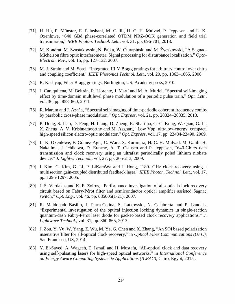
214
[71] H. Hu, P. Münster, E. Palushani, M. Galili, H. C. H. Mulvad, P. Jeppesen and L. K.
Oxenløwe, “640 GBd phase-correlated OTDM NRZ-OOK generation and field trial
transmission,” IEEE Photon. Technol. Lett., vol. 31, pp. 696-701, 2013.
[72] M. Kondrat, M. Szustakowski, N. Pałka, W. Ciurapiński and M. Życzkowski, “A Sagnac-
Michelson fibre optic interferometer: Signal processing for disturbance localization,” Opto-
Electron. Rev., vol. 15, pp. 127-132, 2007.
[73] M. J. Strain and M. Sorel, “Integrated III-V Bragg gratings for arbitrary control over chirp
and coupling coefficient,” IEEE Photonics Technol. Lett., vol. 20, pp. 1863–1865, 2008.
[74] R. Kashyap, Fiber Bragg gratings, Burlington, US: Academy press, 2010.
[75] J. Caraquitena, M. Beltrán, R. Llorente, J. Martí and M. A. Muriel, “Spectral self-imaging
effect by time-domain multilevel phase modulation of a periodic pulse train,” Opt. Lett.,
vol. 36, pp. 858–860, 2011.
[76] R. Maram and J. Azaña, “Spectral self-imaging of time-periodic coherent frequency combs
by parabolic cross-phase modulation,” Opt. Express, vol. 21, pp. 28824–28835, 2013.
[77] P. Dong, S. Liao, D. Feng, H. Liang, D. Zheng, R. Shafiiha, C.-C. Kung, W. Qian, G. Li,
X. Zheng, A. V. Krishnamoorthy and M. Asghari, “Low Vpp, ultralow-energy, compact,
high-speed silicon electro-optic modulator,” Opt. Express, vol. 17, pp. 22484-22490, 2009.
[78] L. K. Oxenløwe, F. Gómez-Agis, C. Ware, S. Kurimura, H. C. H. Mulvad, M. Galili, H.
Nakajima, J. Ichikawa, D. Erasme, A. T. Clausen and P. Jeppesen, “640-Gbit/s data
transmission and clock recovery using an ultrafast periodically poled lithium niobate
device,” J. Lightw. Technol., vol. 27, pp. 205-213, 2009.
[79] I. Kim, C. Kim, G. Li, P. LiKamWa and J. Hong, “180- GHz clock recovery using a
multisection gain-coupled distributed feedback laser,” IEEE Photon. Technol. Lett., vol. 17,
pp. 1295-1297, 2005.
[80] J. S. Vardakas and K. E. Zoiros, “Performance investigation of all-optical clock recovery
circuit based on Fabry-Pérot filter and semiconductor optical amplifier assisted Sagnac
switch,” Opt. Eng., vol. 46, pp. 085005(1-21), 2007.
[81] R. Maldonado-Basilio, J. Parra-Cetina, S. Latkowski, N. Calabretta and P. Landais,
“Experimental investigation of the optical injection locking dynamics in single-section
quantum-dash Fabry-Pérot laser diode for packet-based clock recovery applications,” J.
Lightwave Technol., vol. 31, pp. 860-865, 2013.
[82] J. Zou, Y. Yu, W. Yang, Z. Wu, M. Ye, G. Chen and X. Zhang, “An SOI based polarization
insensitive filter for all-optical clock recovery,” in Optical Fiber Communications (OFC),
San Francisco, US, 2014.
[83] Y. El-Sayed, A. Wageeh, T. Ismail and H. Mostafa, “All-optical clock and data recovery
using self-pulsating lasers for high-speed optical networks,” in International Conference
on Energy Aware Computing Systems & Applications (ICEAC), Cairo, Egypt, 2015 .
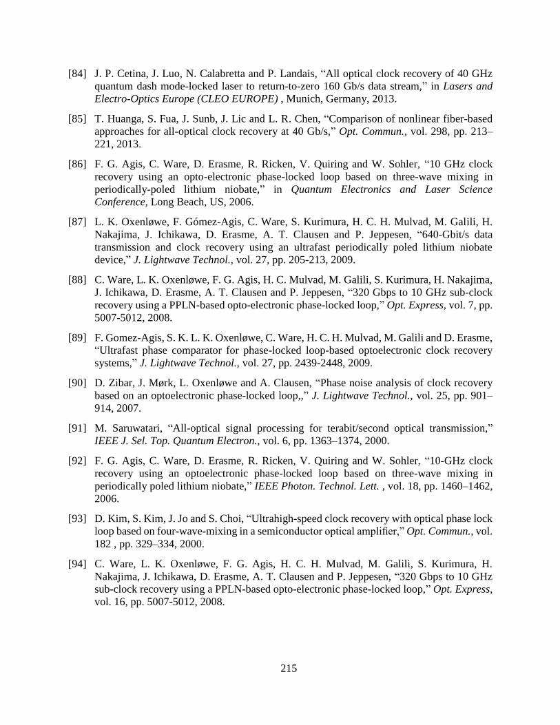
215
[84] J. P. Cetina, J. Luo, N. Calabretta and P. Landais, “All optical clock recovery of 40 GHz
quantum dash mode-locked laser to return-to-zero 160 Gb/s data stream,” in Lasers and
Electro-Optics Europe (CLEO EUROPE) , Munich, Germany, 2013.
[85] T. Huanga, S. Fua, J. Sunb, J. Lic and L. R. Chen, “Comparison of nonlinear fiber-based
approaches for all-optical clock recovery at 40 Gb/s,” Opt. Commun., vol. 298, pp. 213–
221, 2013.
[86] F. G. Agis, C. Ware, D. Erasme, R. Ricken, V. Quiring and W. Sohler, “10 GHz clock
recovery using an opto-electronic phase-locked loop based on three-wave mixing in
periodically-poled lithium niobate,” in Quantum Electronics and Laser Science
Conference, Long Beach, US, 2006.
[87] L. K. Oxenløwe, F. Gómez-Agis, C. Ware, S. Kurimura, H. C. H. Mulvad, M. Galili, H.
Nakajima, J. Ichikawa, D. Erasme, A. T. Clausen and P. Jeppesen, “640-Gbit/s data
transmission and clock recovery using an ultrafast periodically poled lithium niobate
device,” J. Lightwave Technol., vol. 27, pp. 205-213, 2009.
[88] C. Ware, L. K. Oxenløwe, F. G. Agis, H. C. Mulvad, M. Galili, S. Kurimura, H. Nakajima,
J. Ichikawa, D. Erasme, A. T. Clausen and P. Jeppesen, “320 Gbps to 10 GHz sub-clock
recovery using a PPLN-based opto-electronic phase-locked loop,” Opt. Express, vol. 7, pp.
5007-5012, 2008.
[89] F. Gomez-Agis, S. K. L. K. Oxenløwe, C. Ware, H. C. H. Mulvad, M. Galili and D. Erasme,
“Ultrafast phase comparator for phase-locked loop-based optoelectronic clock recovery
systems,” J. Lightwave Technol., vol. 27, pp. 2439-2448, 2009.
[90] D. Zibar, J. Mørk, L. Oxenløwe and A. Clausen, “Phase noise analysis of clock recovery
based on an optoelectronic phase-locked loop,,” J. Lightwave Technol., vol. 25, pp. 901–
914, 2007.
[91] M. Saruwatari, “All-optical signal processing for terabit/second optical transmission,”
IEEE J. Sel. Top. Quantum Electron., vol. 6, pp. 1363–1374, 2000.
[92] F. G. Agis, C. Ware, D. Erasme, R. Ricken, V. Quiring and W. Sohler, “10-GHz clock
recovery using an optoelectronic phase-locked loop based on three-wave mixing in
periodically poled lithium niobate,” IEEE Photon. Technol. Lett. , vol. 18, pp. 1460–1462,
2006.
[93] D. Kim, S. Kim, J. Jo and S. Choi, “Ultrahigh-speed clock recovery with optical phase lock
loop based on four-wave-mixing in a semiconductor optical amplifier,” Opt. Commun., vol.
182 , pp. 329–334, 2000.
[94] C. Ware, L. K. Oxenløwe, F. G. Agis, H. C. H. Mulvad, M. Galili, S. Kurimura, H.
Nakajima, J. Ichikawa, D. Erasme, A. T. Clausen and P. Jeppesen, “320 Gbps to 10 GHz
sub-clock recovery using a PPLN-based opto-electronic phase-locked loop,” Opt. Express,
vol. 16, pp. 5007-5012, 2008.
216
[95] R. Salem, A. Ahmadi, G. Tudury, G. Carter and T. Murphy, “Two-photon absorption for
optical clock recovery in OTDM networks,” J. Lightwave Technol., vol. 24, pp. 3353-3362,
2006.
[96] F. Wang, Y. Yu, Y. Zhang and X. Zhang, “All-optical clock recovery using a single Fabry–
Perot semiconductor optical amplifier,” J. Lightwave Technol., vol. 30, pp. 1632-1637,
2012.
[97] X. Zhou, C. Lu, P. Shum, H. Shalaby, T. Cheng and P. Ye, “A performance analysis of an
all-optical clock extraction circuit based on Fabry–Perot filter,” J. Lightwave Technol., vol.
19, pp. 603–613, 2001.
[98] C. R. Fernández-Pousa, F. Mateos, L. Chantada, M. T. Flores-Arias, C. Bao, M. V. Pérez
and C. Gómez-Reino, “Broadband noise filtering in random sequences of coherent pulses
using the temporal Talbot effect,” J. Opt. Soc. Am. B, vol. 21, pp. 914-922, 2004.
[99] D. Pudo, M. Depa and L. R. Chen, “All-optical clock recovery using the temporal Talbot
effect,” in Optical Fiber Communication (OFC) Conference, Anaheim, USA, 2007.
[100] D. Pudo, M. Depa and L. Chen, “Single and multiwavelength all-optical clock recovery in
single-mode fiber using the temporal Talbot effect,” J. Lightw. Technol., vol. 25, pp. 2898-
2903, 2007.
[101] M. Oiwa, S. Minami, K. Tsuji, N. Onodera and M. Saruwatari, “Study of all-optical clock
recovery performance by the primary and the secondary temporal Talbot effects in a
second-order dispersive medium,” Opt. Fiber Technol., vol. 16, pp. 192–204, 2010.
[102] P. J. Winzer and R. Essiambre, “Advanced modulation formats for high-capacity optical
transport networks,” IEEE Photon. Technol. Lett. , vol. 24, pp. 4711-4728, 2006.
[103] E. Lazzeri, A. T. Nguyen, G. Serafino, N. Kataoka, N. Wada, L. Ascari, A. Bogoni and L.
Potì, “All-optical NRZ-DPSK to RZ-OOK format conversion using optical delay line
interferometer and semiconductor optical amplifier,” in Photonics in Switching Conference,
Monterey, US, 2010.
[104] Y. Ding, H. Hu, M. Galili, J. Xu, L. Liu, M. Pu, H. C. H. Mulvad, L. K. Oxenløwe, C.
Peucheret, P. Jeppesen, X. Zhang, D. Huang and H. Ou, “Generation of a 640 Gbit/s NRZ
OTDM signal using a silicon microring resonator,” Opt. Express, vol. 19, pp. 6471-6477,
2011.
[105] A. Rostami, H. Baghban and R. Maram, Nanostructure semiconductor optical amplifiers:
building blocks for all-optical processing, Berlin, Genmany: Springer-Verlag, 2011.
[106] J. Wang, J. Sun, X. Zhang, D. Huang and M. M. Fejer, “Optical phase erasure and its
application to format conversion through cascaded second-order processes in periodically
poled lithium niobate,” Opt. Lett., vol. 33, pp. 1804-1806, 2008.
[107] Y. Ding, C. Peucheret, M. Pu, B. Zsigri, J. Seoane, L. Liu, J. Xu, H. Ou, X. Zhang and D.
Huang, “Multi-channel WDM RZ-to-NRZ format conversion at 50 Gbit/s based on single
silicon microring resonator,” Opt. Express , vol. 18, pp. 21121-21130, 2010.
217
[108] Y. Zhang, E. Xu, D. Huang and X. Zhang, “All-optical format conversion from RZ to NRZ
utilizing microfiber resonator,” IEEE Photon. Technol. Lett., vol. 21, pp. 1202-1204, 2009.
[109] X. Zhang, Y. Yu, H. Dexiu, L. Lijun and F. Wei, “20-Gb/s all-optical format conversions
from RZ signals with different duty cycles to NRZ signals,” IEEE Photon. Technol. Lett.,
vol. 19, pp. 1027-1029, 2007.
[110] H. Cao, X. Shu, J. Atai, A. Gbadebo, B. Xiong, T. Fan, H. Tang, W. Yang and Y. Yu,
“Optimally-designed single fiber Bragg grating filter scheme for RZ-OOK/DPSK/DQPSK
to NRZ-OOK/DPSK/DQPSK format conversion,” Opt. Express, vol. 22, pp. 30442-30460,
2014.
[111] Z. Y. Zhang, A. E. H. Oehler, B. Resan, S. Kurmulis, K. J. Zhou, Q. Wang, M. Mangold,
T. Süedmeyer, U. Keller, K. J. Weingarten and R. A. Hogg, “1.55 mm InAs/GaAs quantum
dots and high repetition rate quantum dot SESAM mode-locked laser,” Sci. Rep., vol. 2, pp.
477.1-447.5, 2012.
[112] S. Ma, H. S. Z. Chen and N. K. Dutta, “High speed all optical logic gates based on quantum
dot semiconductor optical amplifiers,” Opt. Express, vol. 18, pp. 6417–6422, 2010.
[113] F. Ferdous, H. Miao, D. E. Leaird, K. Srinivasan, J. Wang, L. Chen, L. T. Varghese and A.
M. Weiner, “Spectral line-by-line pulse shaping of on-chip microresonator frequency
combs,” Nat. Photonics, vol. 5, pp. 770–776, 2011.
[114] R. R. Gattass and E. Mazur, “Femtosecond laser micromachining in transparent materials,”
Nat. Photonics, vol. 2, pp. 219–225, 2008.
[115] S. A. Diddams, L. Hollberg and V. Mbele, “Molecular fingerprinting with the resolved
modes of a femtosecond laser frequency comb,” Nature, vol. 445, pp. 627–630, 2007.
[116] P. Grelu and N. Akhmediev, “Dissipative solitons for mode-locked lasers,” Nat. Photonics,
vol. 6, pp. 84–92, 2012.
[117] W. Ng, R. Stephens, O. Persechini and K. V. Reddy, “Ultra-Iow jitter modelocking of Er-
fibre laser at 10 GHz and its application in photonic sampling for analogue-to-digital
conversion,” Electron. Lett. , vol. 37, pp. 113-115, 2001.
[118] L. N. Binh and N. Q. Ngo, Ultra-fast fiber lasers, principles and applications with
MATLAB Models, Boca Raton, FL, USA: CRC Press, 2011.
[119] K. Yiannopoulos, K. Vyrsokinos, E. Kehayas, N. Pleros, K. Vlachos, H. Avramopoulos and
G. Guekos, “Rate multiplication by double-passing Fabry–Pérot filtering,” IEEE Photon.
Technol. Lett., vol. 15, pp. 1294–1296, 2003.
[120] J. Magn, J. Bolger, M. Rochette, S. LaRochelle, L. R. Chen, B. J. Eggleton and J. Azaña,
“Generation of a 4 × 100 GHz Pulse-Train From a Single-Wavelength 10-GHz Mode-
Locked Laser Using Superimposed Fiber Bragg Gratings and Nonlinear Conversion,” IEEE
J. Lightwave Technol., vol. 24, pp. 2091-2099, 2006.
218
[121] H. Tsuda, Y. Tanaka, T. Shioda and T. Kurokawa, “Analog and digital optical pulse
synthesizers using arrayed-waveguide gratings for high-speed optical signal processing,”
IEEE J. Lightwave Technol., vol. 26, pp. 670–677, 2008.
[122] A. Haboucha, W. Zhang, T. Li, M. Lours, A. N. Luiten, Y. L. Coq and G. Santarelli,
“Optical-fiber pulse rate multiplier for ultralow phase-noise signal generation,” Opt. Lett.,
vol. 36, pp. 3654-3656, 2011.
[123] I. Kim, H. Sung and D. Seo, “High-speed optical pulse train generation by line-by-line
spectral intensity and phase coding,” in Opto-Electronics and Communications Conference
(OECC), Busan, Korea, 2012.
[124] D. Kielpinski and O. Gat, “Phase-coherent repetition rate multiplication of a mode-locked
laser from 40 MHz to 1 GHz by injection locking,” Opt. Express, vol. 20, pp. 2717–2724,
2012.
[125] M. Pu, H. Ji, L. H. Frandsen, M. Galili, L. K. Oxenlowe and J. M. Hvam, “High-Q
microring resonator with narrow free spectral range for pulse repetition rate multiplication,”
in Conference on Lasers and Electro-Optics (CLEO), Baltimore, US, 2009.
[126] D. E. Leaird, A. M. Weiner, S. Kamei, M. Ishii, A. Sugita and K. Okamoto, “Generation of
flat-topped 500 GHz pulse bursts using loss engineered arrayed waveguide gratings,” IEEE
Photon. Technol. Lett., vol. 14, pp. 816–818, 2002.
[127] A. Haboucha, W. Zhang, T. Li, M. Lours, A. N. Luiten, Y. L. Coq and G. Santarelli,
“Optical-fiber pulse rate multiplier for ultralow phase-noise signal generation,” Opt. Lett.,
vol. 36, pp. 3654-3656, 2011.
[128] P. D. Heyn, J. Luo, S. D. Lucente, N. Calabretta, H. J. S. Dorren and D. Van-Thourhout,
“In-band label extractor based on cascaded si ring resonators enabling 160Gb/s optical
packet switching modules,” J. Lightwave Technol., vol. 32, pp. 1647-1653, 2014.
[129] H. Teimoori, J. D.Topomondzo, C. Ware and D. Erasme, “Optical packet header processing
using time-to-wavelength mapping in semiconductor optical amplifiers,” J. Lightwave
Technol., vol. 25, pp. 2149-2158, 2007.
[130] M. F. Chiang, Z. Ghassemlooy, H. L. Minh and W. P. Ng, “All-optical packet-switched
routing based on pulse-position-modulated header,” in 7th IASTED International
Conferences on Wireless and Optical Communications (WOC 2007), Montreal, Canada,
2007.
[131] H. F. Talbot, “Facts relating to optical science,” Philos. Mag., vol. 9, pp. 401–407, 1836.
[132] T. Jannson and J. Jannson, “Temporal self-imaging effect in single-mode fibers,” J. Opt.
Soc. Am., vol. 71, pp. 1373–1376, 1981.
[133] F. Mitschke and U. Morgner, “The temporal Talbot effect,” Opt. Photon. News, vol. 9, pp.
45–47, 1998.
219
[134] J. Azaña and M. A. Muriel, “Technique for multiplying the repetition rates of periodic trains
of pulses by means of a temporal self-imaging effect in chirped fiber gratings,” Opt. Lett.,
vol. 24, pp. 1672–1674, 1999.
[135] J. Azaña and M. A. Muriel, “Temporal Talbot effect in fiber gratings and its applications,”
Appl. Opt., vol. 38, pp. 6700–6704, 1999.
[136] J. A. Bolger, P. Hu, J. T. Mok, J. L. Blows and B. J. Eggleton, “Talbot self-imaging and
cross-phase modulation for generation of tunable high repetition rate pulse trains,” Opt.
Commun., vol. 249, pp. 431–439, 2005.
[137] P. A. Andrekson, “Linear propagation of optical picosecond pulse trains over oceanic
distances,” Opt. Lett., vol. 18, pp. 1621-1623 , 1993.
[138] J. J. O'Connor and E. F. Robertson, “William Henry Fox Talbot,” MacTutor History of
Mathematics , 2005. [Online]. Available: http://www-groups.dcs.st-
and.ac.uk/history/Biographies/Talbot.html. [Accessed 10 05 2016].
[139] L. Rayleigh, “On copying diffraction-gratings, and on some phenomenon connected
therewith,” Phil. Mag., vol. 11, pp. 196–205 , 1881.
[140] A. Winkelmann, “Ubereinige erscheinungen, die bei der beugung des lichtesdurch gitter
auftreten,” Ann. Phys. (Leipzig), vol. 332, pp. 905–954, 1908.
[141] H. Weisel, “Uber die nach Fresnelscher art beobachteten beugungser-scheninungen der
gitter,” Ann. Phys. (Leipzig), vol. 338, pp. 995–1031, 1910.
[142] M. Wolfke, “Uber die abbidung eines gitters a erhald der einstellebene,” Ann. Phys.
(Leipzig), vol. 345, pp. 194–200, 1913.
[143] J. M. Cowley and A. F. Moodie, “Fourier images II. The out-of-focus patterns,” Proc. Phys.
Soc. (London), vol. B 70, pp. 497–504, 1957.
[144] W. D. Montgomery, “Self-imaging objects of infinite aperture,” J. Opt. Soc. Am., vol. 57,
pp. 772–778, 1967.
[145] T. Young, “On the theory of light and colours,” Philos. Trans. R. Soc. London, vol. 92, pp.
12-48, 1802.
[146] J. W. Goodman, Introduction to Fourier optics, 2nd ed., New York: McGraw-Hill, 1996.
[147] F. Träger, Springer handbook of lasers and optics, London: Springer, 2012.
[148] J. T. Winthrop and C. R. Worthington, “Theory of Fresnel images. I. Plane periodic objects
in monochromatic light,” J. Opt. Soc. Am., vol. 55, pp. 373–381, 1965.
[149] J. Wen, Y. Zhang and M. Xiao, “The Talbot effect: recent advances in classical optics,
nonlinear optics, and quantum optics,” Adv. Opt. Photonics, vol. 5, pp. 83-130, 2013.
[150] K. Patorski, “The self-imaging phenomenon and its applications,” in Progress in Optics,
vol. 27, Amsterdam, North-Holland, 1989, pp. 1–108.
[151] J. M. Cowley, Diffraction Physics, Amsterdam: North-Holland, 1995.
220
[152] S. A. Akhmanov, A. S. Chirkin, K. N. Drabovich, A. I. Kovrigin, R. V. Khokhlov and A.
P. Sukhorukov, “Nonstationary nonlinear optical effects and ultrashort light pulse
formation,” IEEE J. Quantum Electron., Vols. QE-4, pp. 598-605, 1968.
[153] S. A. Akhmanov, A. P. Sukhorukov and A. S. Chirkin, “Nonstationary phenomena and
space-time analogy in nonlinear optics,” SOU. Phys.-JETP , vol. 28, pp. 748-757, 1969.
[154] B. E. A. Saleh and M. I. Irshid, “Collet–Wolf equivalence theorem and propagation of a
pulse in a single-mode optical fiber,” Opt. Lett., vol. 7, pp. 342–343, 1982.
[155] B. H. Kolner, “Space-time duality and the theory of temporal imaging,” IEEE J. Quantum
Electron., vol. 30, pp. 1951-1963, 1994.
[156] S. Longhi, M. Marano, P. Laporta, O. Svelto, M. Belmonte, B. Agogliati, L. Arcangeli, V.
Pruneri, M. N. Zervas and M. Ibsen, “40-GHz pulse train generation at 1.5 m with a chirped
fiber grating as a frequency multiplier,” Opt. Lett., vol. 25, pp. 1481–1483, 2000.
[157] S. Arahira, S. Kutsuzawa, Y. Matsui, D. Kunimatsu and a. Y. Ogawa, “Repetition-
frequency multiplication of mode-locked pulses using fiber dispersion,” IEEE J. Lightwave
Technol., vol. 16, p. 405–409, 1998.
[158] J. Caraquitena, Z. Jiang, D. E. Leaird and A. M. Weiner, “Tunable pulse repetition-rate
multiplication using phase-only line-by-line pulse shaping,” Opt. Lett., vol. 32, pp. 716–
718, 2007.
[159] J. Azaña, “Spectral Talbot phenomena of frequency combs induced by cross-phase
modulation in optical fibers,” Opt. Lett., vol. 30, pp. 227–229, 2005.
[160] J. M. Lukens, D. E. Leaird and A. M. Weiner, “A temporal cloak at telecommunication data
rate,” Nature, vol. 498, pp. 205–208, 2013.
[161] B. Fischer, B. Vodonos, S. Atkins and A. Bekker, “Dispersion-mode pulsed laser,” Opt.
Lett., vol. 25, pp. 728–730, 2000.
[162] J. Lukens, O. Odele, C. Langrock, M. Fejer, D. Leaird and A. Weiner, “Generation of
biphoton correlation trains through spectral filtering,” Opt. Express, vol. 22, pp. 9585-9596,
2014.
[163] G. Meloni, G. Berrettini, M. Scaffardi and A. Bogoni, “250-times repetition frequency
multiplication for 2.5 THz clock signal generation,” IEEE Electron. Lett., vol. 41, pp. 1294
- 1295, 2005.
[164] J. Magné, J. Bolger, M. Rochette, S. LaRochelle, L. R. Chen, B. J. Eggleton and J. Azaña,
“Generation of a 4 × 100 GHz pulse-train from a single-wavelength 10-GHz mode-locked
laser using superimposed fiber Bragg gratings and nonlinear conversion,” IEEE J.
Lightwave Technol., vol. 24, pp. 2091 - 2099, 2006.
[165] J. Magne, J. Bolger, M. Rochette, S. LaRochelle, L. Chen, B. Eggleton and J. Azana,
“Generation of a 4 × 100 GHz pulse-train from a single-wavelength 10-GHz mode-locked
laser using superimposed fiber Bragg gratings and nonlinear conversion,” IEEE J.
Lightwave Technol., vol. 24, pp. 2091-2099, 2006.
221
[166] J. A. Boiger, P. Hu, J. T. Mok, J. L. Blows and B. J. Eggleton, “Talbot self-imaging and
cross-phase modulation for generation of tunable high repetition rate pulse trains,” Opt.
Commun., vol. 249, pp. 431-439, 2005.
[167] D. Pudo and L. R. Chen, “Tunable passive all-optical pulse repetition rate multiplier using
fiber Bragg gratings,” J. Lightw. Technol., vol. 23, pp. 1729–1733, 2005.
[168] J. H. Lee, Y. Chang, Y. G. Han, S. Kim and S. Lee, “2~5 times tunable repetition-rate
multiplication of a 10 GHz pulse source using a linearly tunable, chirped fiber Bragg
grating,” Opt. Express, vol. 12, pp. 3900–3905, 2004.
[169] P. J. Delfyett, S. Gee, S. Ozharar, F. Quinlan, K. Kim, S. Lee and W. Lee, “Ultrafast
modelocked semiconductor laser - techniques and applications in networking,
instrumentation and signal processing,” in 18th Lasers and Electro-Optics Society Annual
Meeting, 2005.
[170] L. A. Jiang, M. E. Grein, H. A. Haus, E. P. Ippen and H. Yokoyama, “Timing jitter eater
for optical pulse trains,” Opt. Lett., vol. 28, pp. 78-80, 2003.
[171] H. A. Haus and A. Mecozzi, “Noise of mode-locked lasers,” IEEE J. Quantum Electron.,
vol. 29, pp. 983-996, 1993.
[172] M. E. Grein, H. A. Haus, Y. Chen and E. P. Ippen, “Quantum-limited timing jitter in
actively modelocked lasers,” IEEE J. Quantum Electron., vol. 40, pp. 1458-1470, 2004.
[173] T. Yilmaz, C. M. Depriest, A. Braun, J. H. Abeles and P. J. Delfyett, “Noise in fundamental
and harmonic modelocked semiconductor lasers: experiments and simulations,” IEEE J.
Quantum Electron., vol. 39, pp. 838-849, 2003.
[174] S. Gee, F. Quinlan, S. Ozharar and P. J. Delfyett, “Simultaneous optical comb frequency
stabilization and super-mode noise suppression of harmonically mode-locked
semiconductor ring laser using an intracavity etalon,” IEEE Photon. Technol. Lett., vol. 17,
pp. 199-201, 2005.
[175] S. Gee, S. Ozharar, F. Quinlan, J. J. Plant, P. W. Juodawlkis and P. J. Delfyett, “Self-
stabilization of an actively mode-locked semiconductor-based fiber-ring laser for ultralow
jitter,” IEEE Photon. Technol. Lett., vol. 19, pp. 498-500, 2007.
[176] F. Quinlan, S. Gee, S. Ozharar and P. J. Delfyett, “Greater than 20-dB supermode noise
suppression and timing Jitter reduction via CW injection of a harmonically mode-locked
laser,” IEEE Photon. Technol. Lett., vol. 19, pp. 1221-1223, 2007.
[177] M. Mangold, S. M. Link, A. Klenner, C. A. Zaugg, M. Golling, B. W. Tilma and U. Keller,
“Amplitude noise and timing jitter characterization of a high-power mode-locked integrated
external-cavity surface emitting laser,” IEEE Photonics J., vol. 6, pp. 1500309(1-9), 2014.
[178] D. Pudo and L. R. Chen, “Simple estimation of pulse amplitude noise and timing jitter
evolution through the temporal Talbot effect,” Opt. Express, vol. 15, pp. 6351–6357, 2007.
222
[179] C. R. Fernandez-Pousa, F. Mateos, L. Chantada, M. T. Flores-Arias, C. Bao, M. V. Pérez
and C. Gómez-Reino, “Timing jitter smoothing by Talbot effect. I. Variance,” J. Opt. Soc.
Am. B, vol. 21, pp. 1170-1177, 2004.
[180] M. Oiwa, J. Kim, K. Tsuji, N. Onodera and M. Saruwatari, “Experimental demonstration
of timing jitter reduction based on the temporal Talbot effect using LCFBGs,” in
Conference on Lasers and Electro-Optics and Conference on Quantum Electronics and
Laser Science (CLEO/QELS), 2008.
[181] H. G. d. Chatellus, E. Lacot, O. Hugon, O. Jacquin, N. Khebbache and J. Azaña, “Phases
of Talbot patterns in angular self-imaging,” J. Opt. Soc. Am. A, vol. 32, pp. 1132-1139,
2015.
[182] L. R. Cortés, H. G. d. Chatellus and J. Azaña, “On the generality of the Talbot condition
for inducing self-imaging effects on periodic objects,” Opt. Lett., vol. 41, pp. 340-343,
2016.
[183] H. A. Haus and W. S. Wong, “Solitons in optical communications,” Rev. Mod. Phys., vol.
68, pp. 423–444, 1996.
[184] D. R. Solli, C. Ropers, P. Koonath and B. Jalali, “Optical rogue waves,” Nature, vol. 450,
pp. 1054–1057, 2007.
[185] D. Pudo and L. R. Chen, “Tunable passive all-optical pulse repetition rate multiplier using
fiber Bragg gratings,” J. Lightw. Technol., vol. 23, pp. 1729–1733, 2005.
[186] R. Maram, D. Kong, M. Galili, L. K. Oxenløwe and J. Azaña, “Ultrafast all-optical clock
recovery based on phase-only linear optical filtering,” Opt. Lett., vol. 39, pp. 2815–2818,
2014.
[187] S. Tainta, M. Erro, W. Amaya, M. J. Garde, S. Sales and M. A. Muriel, “Periodic time-
domain modulation for the electrically tunable control of optical pulse train envelope and
repetition rate multiplication,” J. Sel. Top. Quantum., vol. 18, pp. 377-383, 2012.
[188] R. Maram, J. V. Howe, M. Li and J. Azaña, “Noiseless intensity amplification of repetitive
signals by coherent addition using the temporal Talbot effect,” Nat. Commun., vol. 5, pp.
4827(1-10), 2014.
[189] A. Malacarne and J. Azaña, “Discretely tunable comb spacing of a frequency comb by
multilevel phase modulation of a periodic pulse train,” Opt. Express, vol. 21, pp. 4139–
4144, 2013.
[190] R. J. Essiambre, G. Kramer, P. J. Winzer, G. J. Foschini and B. Goebel, “Capacity limits of
optical fibre networks,” J. Lightwave Technol., vol. 28, pp. 662-701, 2010.
[191] F. Ferdous, H. Miao, D. E. Leaird, K. Srinivasan, J. Wang, L. Chen, L. T. Varghese and A.
M. Weiner, “Spectral line-by-line pulse shaping of on-chip microresonator frequency
combs,” Nat. Photonics, vol. 5, pp. 770-776, 2011.
223
[192] A. Haboucha, W. Zhang, T. Li, M. Lours, A. N. Luiten, Y. Le Coq and G. Santarelli,
“Optical-fiber pulse rate multiplier for ultralow phase-noise signal generation,” Opt. Lett.,
vol. 36, pp. 3654-3656, 2011.
[193] F. Helmchen and W. Denk, “Deep tissue two-photon microscopy,” Nat. Methods, vol. 2,
pp. 932-940, 2005.
[194] J. Cheng, C. Liua, S. Shangb, D. Liub, W. Perrieb, G. Deardenb and K. Watkinsb, “A
review of ultrafast laser materials micromachining,” Opt. & Laser Technol., vol. 46, pp.
88-102, 2013.
[195] G. A. Mourou, T. Tajima and S. V. Bulanov, “Optics in the relativistic regime,” Rev. Mod.
Phys. , vol. 78, pp. 309-371, 2006.
[196] L. Yan, A. E. Willner, X. Wu, A. Yi, A. Bogoni, Z.-Y. Chen and H.-Y. Jiang, “All-optical
signal processing for ultrahigh speed optical systems and networks,” J. Lightwave Technol.,
vol. 30, pp. 3760-3770, 2012.
[197] R. S. Tucker, “Green optical communications—Part I: Energy limitations in transport,”
IEEE J. Sel. Top. Quant. Electron., vol. 17, pp. 245-260, 2011.
[198] B. Jalali and S. Fathpour, “Silicon photonics,” J. Lightwave Technol., vol. 24, pp. 4600-
4615, 2006.
[199] L. De Forest, “The audion-detector and amplifier,” Proc. of the IEEE, vol. 2, pp. 19-25,
1914.
[200] J. Bardeen and W. H. Brattain, “The transistor, a semi-conductor triode,” Phys. Rev. Lett.,
vol. 74, pp. 230-231, 1948.
[201] R. J. Mears, L. Reekie, M. Jauncey and D. N. Payne, “Low-noise erbium-doped fiber
amplifier operating at 1.54 μm,” Electron. Lett., vol. 26, pp. 1026-1028, 1987.
[202] M. Kozuma, Y. Suzuki, Y. Torii, T. Sugiura, T. Kuga, E. W. Hagley and L. Deng, “Phase-
coherent amplification of matter waves,” Science , vol. 286, pp. 2309-2312, 1999.
[203] C. Joachim, J. K. Gimzewski and A. Aviram, “Electronics using hybrid-molecular and
mono-molecular devices,” Nature , vol. 408, pp. 541-548, 2000.
[204] M. A. Foster, A. C. Turner, J. E. Sharping, B. S. Schmidt, M. Lipson and A. L. Gaeta,
“Broad-band optical parametric gain on a silicon photonic chip,” Nature , vol. 441, pp. 960-
963, 2006.
[205] R. P. Beardsley, A. V. Akimov, M. Henini and A. J. Kent, “Coherent terahertz sound
amplification and spectral line narrowing in a Stark ladder superlattice,” Phys. Rev. Lett.,
vol. 104, pp. 085501(1-4), 2010.
[206] Z. Tong, C. Lundström, P. A. Andrekson, C. J. McKinstrie, M. Karlsson, D. J. Blessing, E.
Tipsuwannakul, B. J. Puttnam, H. Toda and L. Grüner-Nielsen, “Towards ultrasensitive
optical links enabled by low-noise phase-sensitive amplifiers,” Nat. Photonics, vol. 5, pp.
430-436, 2011.
224
[207] T. Eidam, J. Rothhardt, F. Stutzki, F. Jansen, S. Hädrich, H. Carstens, C. Jauregui, J.
Limpert and A. Tünnermann, “Fiber chirped-pulse amplification system emitting 3.8 GW
peak power,” Opt. Express, vol. 19, pp. 255-260, 2011.
[208] J. Tümmler, R. Jung, H. Stiel, P. V. Nickles and W. Sandner, “High-repetition-rate chirped-
pulse-amplification thin-disk laser system with joule-level pulse energy,” Opt. Lett., vol.
34, pp. 1378-1380, 2009.
[209] Y. Vidne, M. Rosenbluh and T. W. Hansch, “Pulse picking by phase-coherent additive
pulse generation in an external cavity,” Opt. Lett., vol. 28, pp. 2396-2398, 2003.
[210] H. A. Haus, “The proper definition of noise figure of optical amplifiers,” in Optical
Amplifiers and Their Applications, OSA/OAA, Québec, Canada, 2000.
[211] J. R. Jones and J. Ye, “Femtosecond pulse amplification by coherent addition in a passive
optical cavity,” Opt. Lett., vol. 27, pp. 1848-1850, 2002.
[212] R. Maram, J. Van Howe and J. Azaña, “Noise-eating amplifier for repetitive signals,” in
IEEE photonic conference (IPC), San Diego, USA, 2014.
[213] P. AB, “http://www.proximion.com/Products/DCM-HDC,” 2014.
[214] J. P. Heritage and A. M. Weiner, “Advances in spectral code-division multiple access
communications,” IEEE J. Sel. Top. Quantum Electron., vol. 13, pp. 1351-1369, 2007.
[215] J. D. Jackson, Classical Electrodynamics, New York, US: Wiley, 1998.
[216] W. M. Robertson, C. Baker and C. B. Bennett, “Slow group velocity propagation of sound
via defect coupling in a one-dimensional acoustic band gap array,” Am. J. Phys., vol. 72,
pp. 255-257, 2004.
[217] A. D. Cronin, J. Schmiedmayer and D. E. Pritchard, “Optics and interferometry with atoms
and molecules,” Rev. Mod. Phys., vol. 81, pp. 1051-1129, 2009.
[218] L. Deng, E. W. Hagley, J. Denschlag, J. E. Simsarian, M. Edwards, C. W. Clark, K.
Helmerson, S. L. Rolston and W. D. Phillips, “Temporal, matter-wave-dispersion Talbot
effect,” Phys. Rev. Lett., vol. 83, pp. 5407-5411, 1999.
[219] M. J. Madou, From MEMS to Bio-MEMS and Bio-NEMS: manufacturing techniques and
applications, Boca Raton, FL, USA: CRC Press, 2011.
[220] P. Kolchin, C. Belthangady, S. Du, G. Y. Yin and S. E. Harris, “Electro-optic modulation
of single photons,” Phys. Rev. Lett., vol. 101, pp. 103601(1-4), 2008.
[221] J. Luo, N. Calabretta, J. Parra-Cetina, S. Latkowski, R. Maldonado-Basilio, P. Landais and
H. J. S. Dorren, “320 Gb/s all-optical clock recovery and time de-multiplexing after
transmission enabled bysingle quantum dash mode-locked laser,” Opt. Lett., vol. 38, pp.
4805-4808, 2013.
[222] Z. Wang and S. Fan, “Compact all-pass filters in photonic crystals as the building block for
high-capacity optical delay lines,” Phys. Rev., vol. 68, pp. 066616 , 2003.
225
[223] J. T. Willits, A. M. Weiner and S. T. Cundiff, “Line-by-line pulse shaping with spectral
resolution below 890 MHz,” Opt. Express, vol. 20, pp. 3110-3117, 2012.
[224] L. K. Oxenløwe, R. Slavık, M. Galili, H. C. H. Mulvad, A. T. Clausen, Y. Park, J. Azana
and P. Jeppesen, “640 Gb/s timing jitter-tolerant data processing using a long-period fiber-
Grating-based flat-top pulse shaper,” IEEE J. Sel. Top. Quant. Electron., vol. 14, pp. 566-
572, 2008.
[225] J. H. Lee, Y. Chang, Y.-G. Han, S. Kim and S. Lee, “2~5 times tunable repetition-rate
multiplication of a 10 GHz pulse source using a linearly tunable, chirped fiber Bragg
grating,” Opt. Express, vol. 12, pp. 3900–3905, 2004.
[226] C. J. S. de-Matos and J. R. Taylor, “Tunable repetition-rate multiplication of a 10 GHz
pulse train using linear and nonlinear fiber propagation,” Appl. Phys. Lett., vol. 38, pp.
5356–5358, 2003.
[227] J. Caraquitena and J. Martí, “High-rate pulse-train generation by phase-only filtering of an
electrooptic frequency comb: analysis and optimization,” Opt. Commun., vol. 282, pp.
3686–3692, 2009.
[228] H. Hu, H. C. H. Mulvad, M. Galili, E. Palushani, J. Xu, A. T. Clausen, L. K. Oxenlowe and
P. Jeppesen, “Polarization- insensitive 640Gb/s demultiplexing based on four wave mixing
in a polarization-maintaining fibre loop,” J. Lightw. Technol., vol. 28, pp. 1789-1795, 2010.
[229] A. M. de-Melo, S. Randel and K. Petermann, “Mach–Zehnder interferometer-based high-
speed OTDM add–drop multiplexing,” J. Lightw. Technol., vol. 25, pp. 1017–1026, 2007.
[230] J. Parra-Cetina, J. Luo, N. Calabretta, S. Latkowski, H. J. S. Dorren and P. Landais,
“Subharmonic all-optical clock recovery of up to 320 Gb/s signal using a quantum dash
Fabry–Perot mode-locked laser,” Electron. Lett., vol. 31, pp. 3127–3134, 2013.
[231] M. Oiwa, S. Minami, K. Tsuji, N. Onodera and M. Saruwatari, “Temporal-Talbot-effect-
based preprocessing for pattern-effect reduction in all-optical clock recovery using a
semiconductor-optical-amplifier-based fiber ring laser,” Optical Fiber Technol., vol. 16,
pp. 63-71, 2010.
[232] R. Maram and J. Azaña, “Spectral self-imaging of time-periodic coherent frequency combs
by parabolic cross-phase modulation,” Opt. Express, vol. 21, pp. 28824–28835, 2013.
[233] R. Maram, D. Kong, M. Galili, L. K. Oxenløwe and J. Azaña, “Ultrafast all-optical cock
recovery based on phase-only linear optical filtering,” Opt. Lett., vol. 39, pp. 2815-2818,
2014.
[234] I. P. Kaminow, T. Li and A. E. Willner, Optical fiber telecommunications VB: systems and
networks, San Diego, US: Academic press, 2010.