Embed Size (px)
Citation preview
preliminary
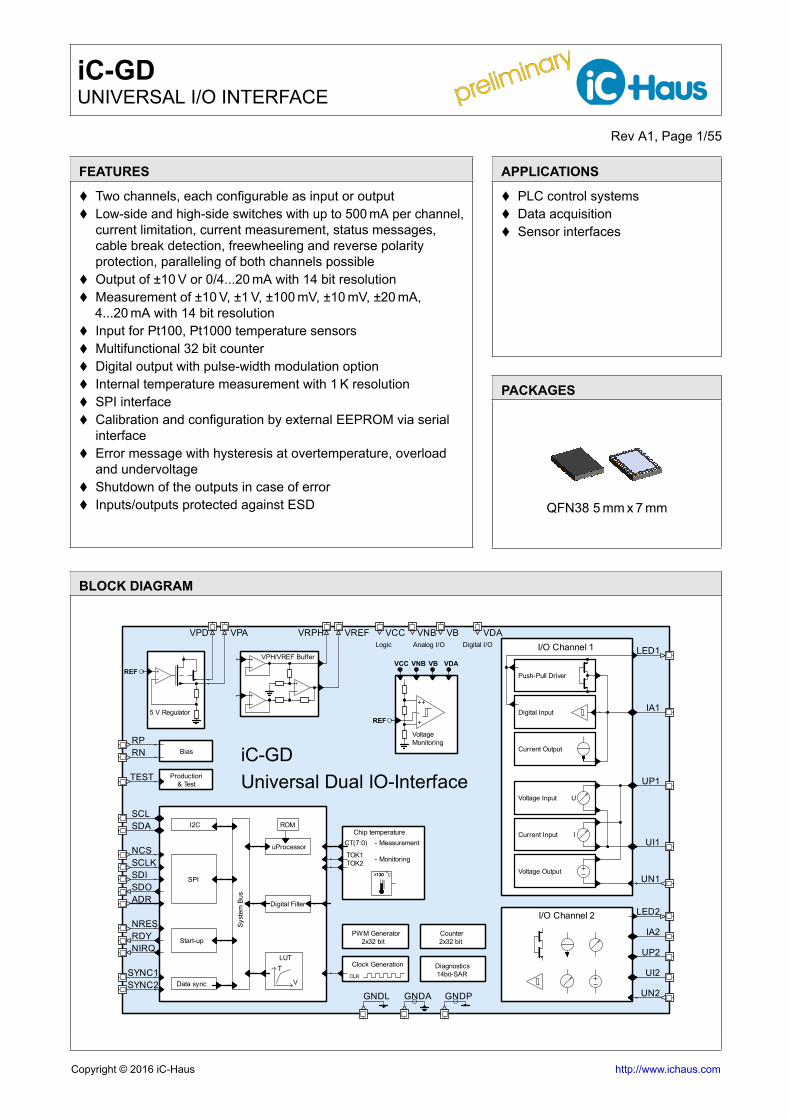
preliminary iC-GDUNIVERSAL I/O INTERFACE
Rev A1, Page 1/55
FEATURES
Two channels, each configurable as input or output Low-side and high-side switches with up to 500 mA per channel,
current limitation, current measurement, status messages,cable break detection, freewheeling and reverse polarityprotection, paralleling of both channels possible
Output of ±10 V or 0/4...20 mA with 14 bit resolution Measurement of ±10 V, ±1 V, ±100 mV, ±10 mV, ±20 mA,
4...20 mA with 14 bit resolution Input for Pt100, Pt1000 temperature sensors Multifunctional 32 bit counter Digital output with pulse-width modulation option Internal temperature measurement with 1 K resolution SPI interface Calibration and configuration by external EEPROM via serial
interface Error message with hysteresis at overtemperature, overload
and undervoltage Shutdown of the outputs in case of error Inputs/outputs protected against ESD
APPLICATIONS
PLC control systems Data acquisition Sensor interfaces
PACKAGES
dra_qfn38-1_pack_2, 2.4:1
QFN38 5 mm x 7 mm
BLOCK DIAGRAM
ROM
I/O Channel 1Analog I/OLogic
Syst
em B
us
V
iC-GD
Digital Filter
Bias
Chip temperature
- Monitoring
Voltage Output
Push-Pull Driver
Digital Input
Voltage Input
Current Input
U
I
Digital I/O
I/O Channel 2
Start-up
Data sync
Universal Dual IO-Interface
T
Monitoring
LUT
SPI
Counter2x32 bit
PWM Generator2x32 bit
I2C
Clock Generation14bit-SARDiagnostics
VPH/VREF Buffer
& Test
- MeasurementuProcessor
RN
SDA
UI1
Current Output
5 V Regulator
Production
Voltage
VNB VDAVCCVREF VB
RP
SDO
CLK
SDI UN1
TOK2TOK1
RDY
VRPH
CT(7:0)
UI2
LED2
UP2
UN2
TEST
ADR
IA1
VPA
SYNC1
GNDL GNDPGNDA
NRESIA2
VPD
SYNC2
SCLK
LED1
NIRQ
NCS
UP1
SCL
++-+
>130
VCC VNBREF
REF
VDAVB
C>130
Copyright © 2016 iC-Haus http://www.ichaus.com
preliminary
preliminary iC-GDUNIVERSAL I/O INTERFACE
Rev A1, Page 2/55
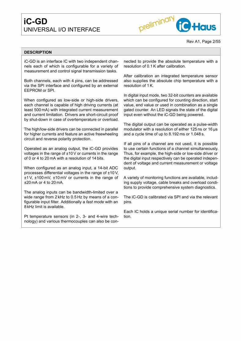
DESCRIPTION
iC-GD is an interface IC with two independent chan-nels each of which is configurable for a variety ofmeasurement and control signal transmission tasks.
Both channels, each with 4 pins, can be addressedvia the SPI interface and configured by an externalEEPROM or SPI.
When configured as low-side or high-side drivers,each channel is capable of high driving currents (atleast 500 mA) with integrated current measurementand current limitation. Drivers are short-circuit proofby shut-down in case of overtemperature or overload.
The high/low-side drivers can be connected in parallelfor higher currents and feature an active freewheelingcircuit and reverse polarity protection.
Operated as an analog output, the iC-GD providesvoltages in the range of ±10 V or currents in the rangeof 0 or 4 to 20 mA with a resolution of 14 bits.
When configured as an analog input, a 14-bit ADCprocesses differential voltages in the range of ±10 V,±1 V, ±100 mV, ±10 mV or currents in the range of±20 mA or 4 to 20 mA.
The analog inputs can be bandwidth-limited over awide range from 2 kHz to 0.5 Hz by means of a con-figurable input filter. Additionally a fast mode with an8 kHz limit is available.
Pt temperature sensors (in 2-, 3- and 4-wire tech-nology) and various thermocouples can also be con-
nected to provide the absolute temperature with aresolution of 0.1 K after calibration.
After calibration an integrated temperature sensoralso supplies the absolute chip temperature with aresolution of 1 K.
In digital input mode, two 32-bit counters are availablewhich can be configured for counting direction, startvalue, end value or used in combination as a singlegated counter. An LED signals the state of the digitalinput even without the iC-GD being powered.
The digital output can be operated as a pulse-widthmodulator with a resolution of either 125 ns or 16µsand a cycle time of up to 8.192 ms or 1.048 s.
If all pins of a channel are not used, it is possibleto use certain functions of a channel simultaneously.Thus, for example, the high-side or low-side driver orthe digital input respectively can be operated indepen-dent of voltage and current measurement or voltageoutput.
A variety of monitoring functions are available, includ-ing supply voltage, cable breaks and overload condi-tions to provide comprehensive system diagnostics.
The iC-GD is calibrated via SPI and via the relevantpins.
Each IC holds a unique serial number for identifica-tion.
preliminary
preliminary iC-GDUNIVERSAL I/O INTERFACE
Rev A1, Page 3/55
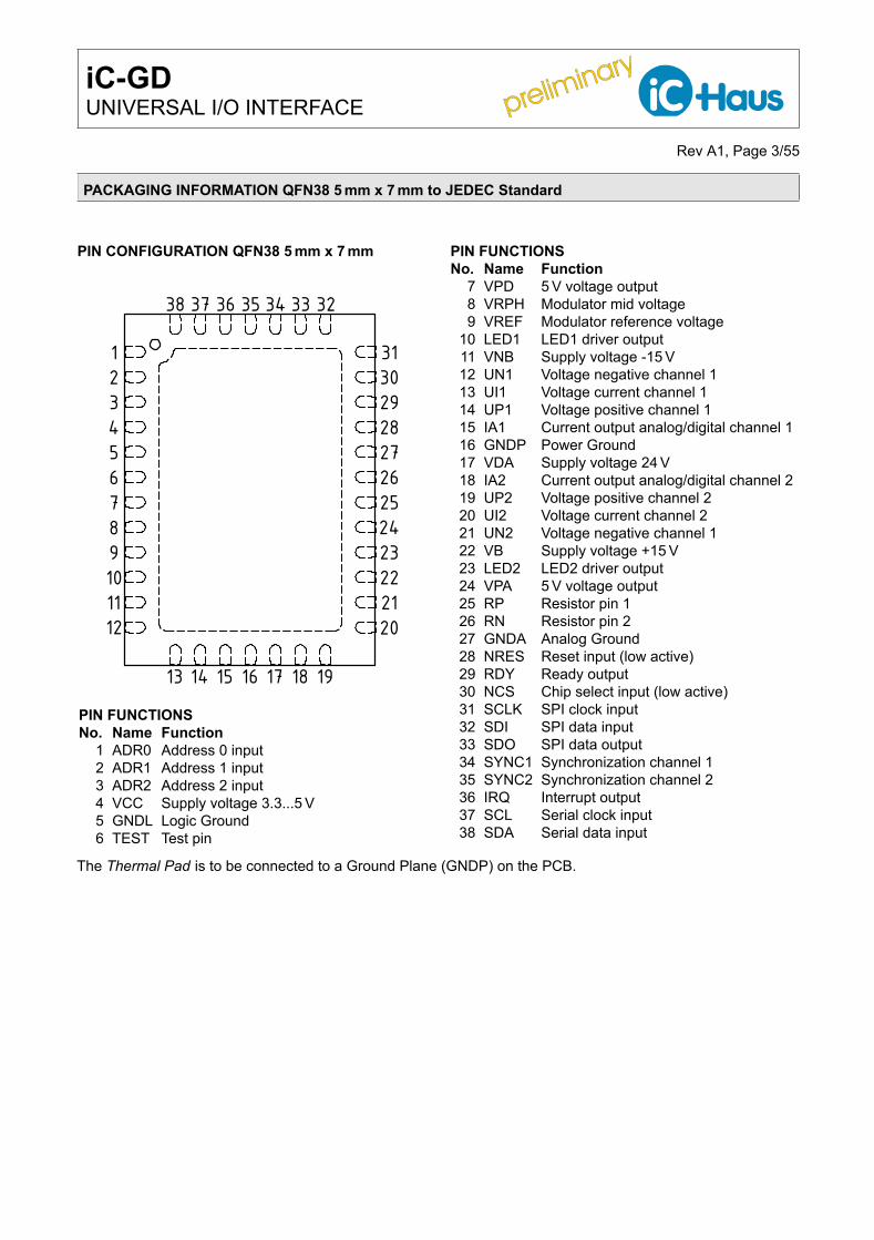
PACKAGING INFORMATION QFN38 5 mm x 7 mm to JEDEC Standard
PIN CONFIGURATION QFN38 5 mm x 7 mm
123456789101112
13 14 15 16 17 18 19
202122232425262728293031
32333435363738
PIN FUNCTIONSNo. Name Function
1 ADR0 Address 0 input2 ADR1 Address 1 input3 ADR2 Address 2 input4 VCC Supply voltage 3.3...5 V5 GNDL Logic Ground6 TEST Test pin
PIN FUNCTIONSNo. Name Function
7 VPD 5 V voltage output8 VRPH Modulator mid voltage9 VREF Modulator reference voltage
10 LED1 LED1 driver output11 VNB Supply voltage -15 V12 UN1 Voltage negative channel 113 UI1 Voltage current channel 114 UP1 Voltage positive channel 115 IA1 Current output analog/digital channel 116 GNDP Power Ground17 VDA Supply voltage 24 V18 IA2 Current output analog/digital channel 219 UP2 Voltage positive channel 220 UI2 Voltage current channel 221 UN2 Voltage negative channel 122 VB Supply voltage +15 V23 LED2 LED2 driver output24 VPA 5 V voltage output25 RP Resistor pin 126 RN Resistor pin 227 GNDA Analog Ground28 NRES Reset input (low active)29 RDY Ready output30 NCS Chip select input (low active)31 SCLK SPI clock input32 SDI SPI data input33 SDO SPI data output34 SYNC1 Synchronization channel 135 SYNC2 Synchronization channel 236 IRQ Interrupt output37 SCL Serial clock input38 SDA Serial data input
The Thermal Pad is to be connected to a Ground Plane (GNDP) on the PCB.
preliminary
preliminary iC-GDUNIVERSAL I/O INTERFACE
Rev A1, Page 4/55
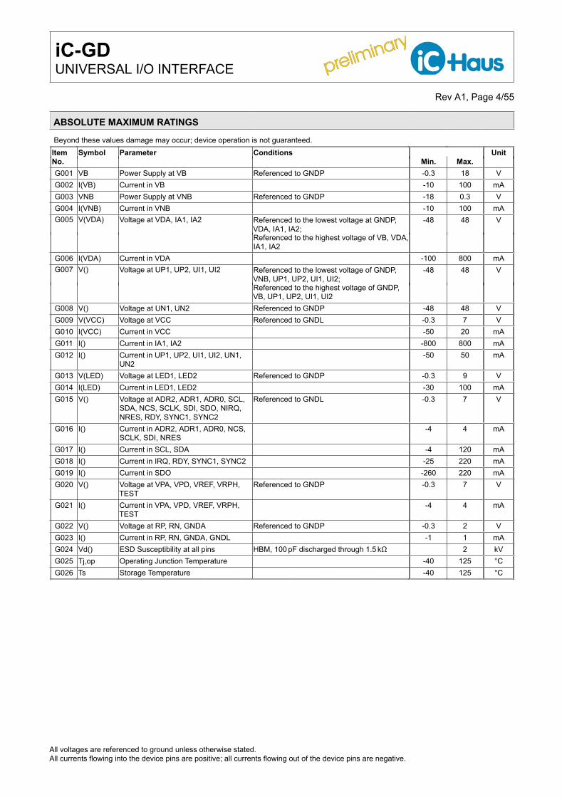
ABSOLUTE MAXIMUM RATINGS
Beyond these values damage may occur; device operation is not guaranteed.Item Symbol Parameter Conditions UnitNo. Min. Max.G001 VB Power Supply at VB Referenced to GNDP -0.3 18 VG002 I(VB) Current in VB -10 100 mAG003 VNB Power Supply at VNB Referenced to GNDP -18 0.3 VG004 I(VNB) Current in VNB -10 100 mAG005 V(VDA) Voltage at VDA, IA1, IA2 Referenced to the lowest voltage at GNDP,
VDA, IA1, IA2;-48 48 V
Referenced to the highest voltage of VB, VDA,IA1, IA2
G006 I(VDA) Current in VDA -100 800 mAG007 V() Voltage at UP1, UP2, UI1, UI2 Referenced to the lowest voltage of GNDP,
VNB, UP1, UP2, UI1, UI2;-48 48 V
Referenced to the highest voltage of GNDP,VB, UP1, UP2, UI1, UI2
G008 V() Voltage at UN1, UN2 Referenced to GNDP -48 48 VG009 V(VCC) Voltage at VCC Referenced to GNDL -0.3 7 VG010 I(VCC) Current in VCC -50 20 mAG011 I() Current in IA1, IA2 -800 800 mAG012 I() Current in UP1, UP2, UI1, UI2, UN1,
UN2-50 50 mA
G013 V(LED) Voltage at LED1, LED2 Referenced to GNDP -0.3 9 VG014 I(LED) Current in LED1, LED2 -30 100 mAG015 V() Voltage at ADR2, ADR1, ADR0, SCL,
SDA, NCS, SCLK, SDI, SDO, NIRQ,NRES, RDY, SYNC1, SYNC2
Referenced to GNDL -0.3 7 V
G016 I() Current in ADR2, ADR1, ADR0, NCS,SCLK, SDI, NRES
-4 4 mA
G017 I() Current in SCL, SDA -4 120 mAG018 I() Current in IRQ, RDY, SYNC1, SYNC2 -25 220 mAG019 I() Current in SDO -260 220 mAG020 V() Voltage at VPA, VPD, VREF, VRPH,
TESTReferenced to GNDP -0.3 7 V
G021 I() Current in VPA, VPD, VREF, VRPH,TEST
-4 4 mA
G022 V() Voltage at RP, RN, GNDA Referenced to GNDP -0.3 2 VG023 I() Current in RP, RN, GNDA, GNDL -1 1 mAG024 Vd() ESD Susceptibility at all pins HBM, 100 pF discharged through 1.5 kΩ 2 kVG025 Tj,op Operating Junction Temperature -40 125 °CG026 Ts Storage Temperature -40 125 °C
All voltages are referenced to ground unless otherwise stated.All currents flowing into the device pins are positive; all currents flowing out of the device pins are negative.
preliminary
preliminary iC-GDUNIVERSAL I/O INTERFACE
Rev A1, Page 5/55
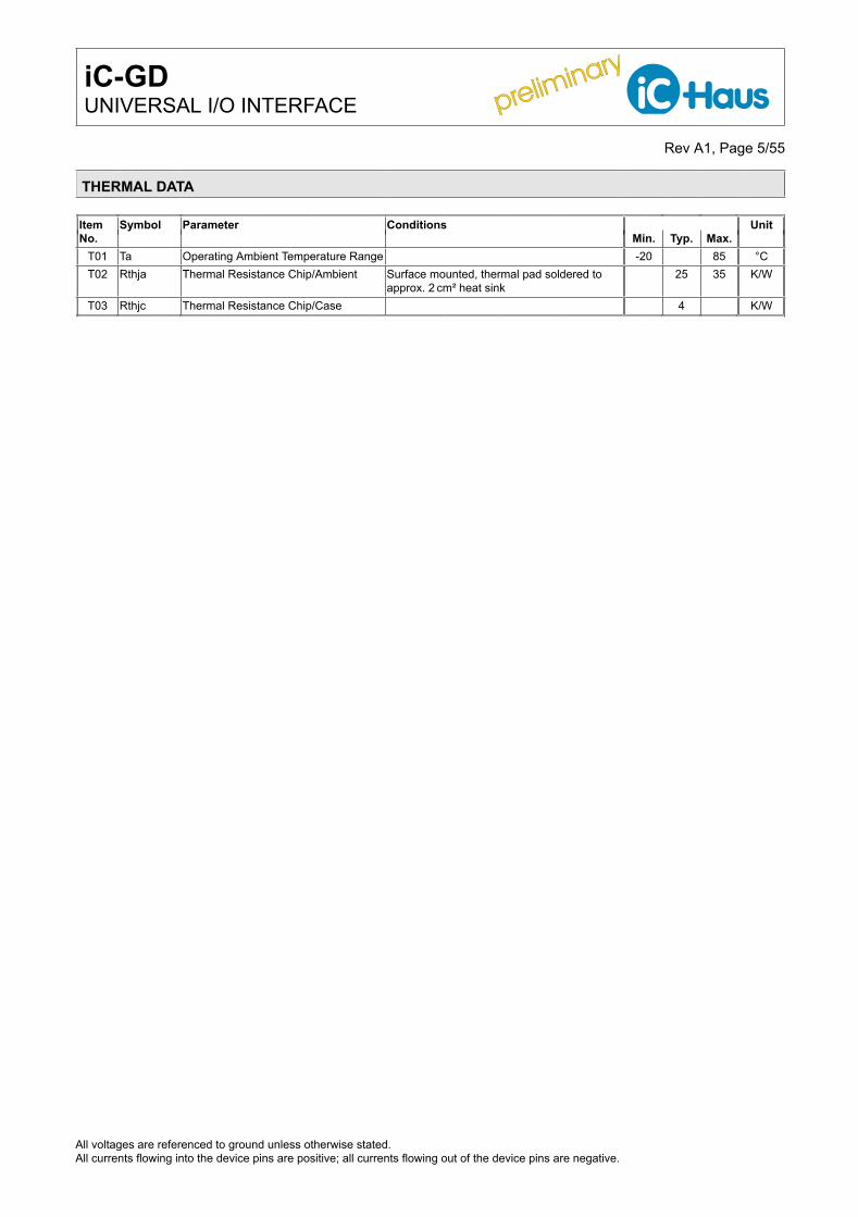
THERMAL DATA
Item Symbol Parameter Conditions UnitNo. Min. Typ. Max.
T01 Ta Operating Ambient Temperature Range -20 85 °CT02 Rthja Thermal Resistance Chip/Ambient Surface mounted, thermal pad soldered to
approx. 2 cm² heat sink25 35 K/W
T03 Rthjc Thermal Resistance Chip/Case 4 K/W
All voltages are referenced to ground unless otherwise stated.All currents flowing into the device pins are positive; all currents flowing out of the device pins are negative.
preliminary
preliminary iC-GDUNIVERSAL I/O INTERFACE
Rev A1, Page 6/55
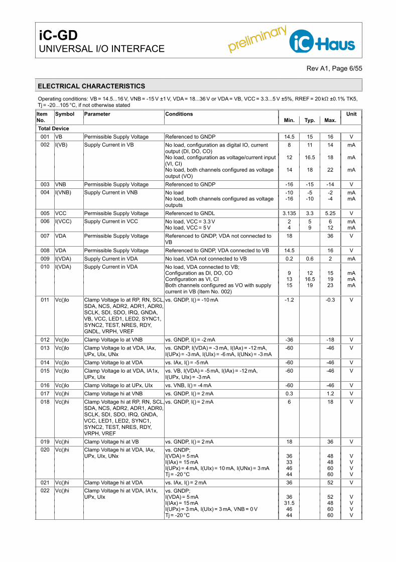
ELECTRICAL CHARACTERISTICS
Operating conditions: VB = 14.5...16 V, VNB = -15 V ±1 V, VDA = 18...36 V or VDA = VB, VCC = 3.3...5 V ±5%, RREF = 20 kΩ ±0.1% TK5,Tj = -20...105 °C, if not otherwise statedItem Symbol Parameter Conditions UnitNo. Min. Typ. Max.Total Device001 VB Permissible Supply Voltage Referenced to GNDP 14.5 15 16 V002 I(VB) Supply Current in VB No load, configuration as digital IO, current
output (DI, DO, CO)8 11 14 mA
No load, configuration as voltage/current input(VI, CI)
12 16.5 18 mA
No load, both channels configured as voltageoutput (VO)
14 18 22 mA
003 VNB Permissible Supply Voltage Referenced to GNDP -16 -15 -14 V004 I(VNB) Supply Current in VNB No load -10 -5 -2 mA
No load, both channels configured as voltageoutputs
-16 -10 -4 mA
005 VCC Permissible Supply Voltage Referenced to GNDL 3.135 3.3 5.25 V006 I(VCC) Supply Current in VCC No load, VCC = 3.3 V 2 5 6 mA
No load, VCC = 5 V 4 9 12 mA007 VDA Permissible Supply Voltage Referenced to GNDP, VDA not connected to
VB18 36 V
008 VDA Permissible Supply Voltage Referenced to GNDP, VDA connected to VB 14.5 16 V009 I(VDA) Supply Current in VDA No load, VDA not connected to VB 0.2 0.6 2 mA010 I(VDA) Supply Current in VDA No load, VDA connected to VB;
Configuration as DI, DO, CO 9 12 15 mAConfiguration as VI, CI 13 16.5 19 mABoth channels configured as VO with supplycurrent in VB (Item No. 002)
15 19 23 mA
011 Vc()lo Clamp Voltage lo at RP, RN, SCL,SDA, NCS, ADR2, ADR1, ADR0,SCLK, SDI, SDO, IRQ, GNDA,VB, VCC, LED1, LED2, SYNC1,SYNC2, TEST, NRES, RDY,GNDL, VRPH, VREF
vs. GNDP, I() = -10 mA -1.2 -0.3 V
012 Vc()lo Clamp Voltage lo at VNB vs. GNDP, I() = -2 mA -36 -18 V013 Vc()lo Clamp Voltage lo at VDA, IAx,
UPx, UIx, UNxvs. GNDP, I(VDA) = -3 mA, I(IAx) = -12 mA,I(UPx) = -3 mA, I(UIx) = -6 mA, I(UNx) = -3 mA
-60 -46 V
014 Vc()lo Clamp Voltage lo at VDA vs. IAx, I() = -5 mA -60 -46 V015 Vc()lo Clamp Voltage lo at VDA, IA1x,
UPx, UIxvs. VB, I(VDA) = -5 mA, I(IAx) = -12 mA,I(UPx, UIx) = -3 mA
-60 -46 V
016 Vc()lo Clamp Voltage lo at UPx, UIx vs. VNB, I() = -4 mA -60 -46 V017 Vc()hi Clamp Voltage hi at VNB vs. GNDP, I() = 2 mA 0.3 1.2 V018 Vc()hi Clamp Voltage hi at RP, RN, SCL,
SDA, NCS, ADR2, ADR1, ADR0,SCLK, SDI, SDO, IRQ, GNDA,VCC, LED1, LED2, SYNC1,SYNC2, TEST, NRES, RDY,VRPH, VREF
vs. GNDP, I() = 2 mA 6 18 V
019 Vc()hi Clamp Voltage hi at VB vs. GNDP, I() = 2 mA 18 36 V020 Vc()hi Clamp Voltage hi at VDA, IAx,
UPx, UIx, UNxvs. GNDP;I(VDA) = 5 mA 36 48 VI(IAx) = 15 mA 33 48 VI(UPx) = 4 mA, I(UIx) = 10 mA, I(UNx) = 3 mA 46 60 VTj = -20 °C 44 60 V
021 Vc()hi Clamp Voltage hi at VDA vs. IAx, I() = 2 mA 36 52 V022 Vc()hi Clamp Voltage hi at VDA, IA1x,
UPx, UIxvs. GNDP;I(VDA) = 5 mA 36 52 VI(IAx) = 15 mA 31.5 48 VI(UPx) = 3 mA, I(UIx) = 3 mA, VNB = 0 V 46 60 VTj = -20 °C 44 60 V
preliminary
preliminary iC-GDUNIVERSAL I/O INTERFACE
Rev A1, Page 7/55
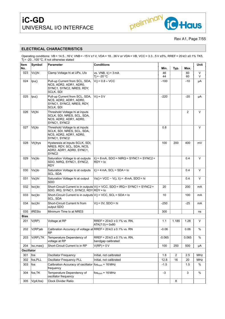
ELECTRICAL CHARACTERISTICS
Operating conditions: VB = 14.5...16 V, VNB = -15 V ±1 V, VDA = 18...36 V or VDA = VB, VCC = 3.3...5 V ±5%, RREF = 20 kΩ ±0.1% TK5,Tj = -20...105 °C, if not otherwise statedItem Symbol Parameter Conditions UnitNo. Min. Typ. Max.
023 Vc()hi Clamp Voltage hi at UPx, UIx vs. VNB, I() = 3 mA 46 60 VTj = -20 °C 44 60 V
024 Ipu() Pull-up Current from SCL, SDA,NCS, ADR2, ADR1, ADR0,SYNC1, SYNC2, NRES, RDY,SCLK, SDI
V() = 0.8 ∗ VCC -100 -10 µA
025 Ipu() Pull-up Current from SCL, SDA,NCS, ADR2, ADR1, ADR0,SYNC1, SYNC2, NRES, RDY,SCLK, SDI
V() = 0 V -220 -20 µA
026 Vt()hi Threshold Voltage hi at inputsSCLK, SDI, NRES, SCL, SDA,NCS, ADR2, ADR1, ADR0,SYNC1, SYNC2
2 V
027 Vt()lo Threshold Voltage lo at inputsSCLK, SDI, NRES, SCL, SDA,NCS, ADR2, ADR1, ADR0,SYNC1, SYNC2
0.8 V
028 Vt()hys Hysteresis at inputs SCLK, SDI,NRES, RDY, SCL, SDA, NCS,ADR2, ADR1, ADR0, SYNC1,SYNC2
100 200 400 mV
029 Vs()lo Saturation Voltage lo at outputsSDO, NIRQ, SYNC1, SYNC2,RDY
I() = 8 mA, SDO = NIRQ = SYNC1 = SYNC2 =RDY = lo
0.4 V
030 Vs()lo Saturation Voltage lo at outputsSCL, SDA
I() = 4 mA, SCL = SDA = lo 0.4 V
031 Vs()hi Saturation Voltage hi at outputSDO
Vs() = VCC − V(), I() = -8 mA, SDO = hi 0.4 V
032 Isc()lo Short-Circuit Current lo in outputsSDO, IRQ, SYNC1, SYNC2, RDY
V() = VCC, SDO = IRQ = SYNC1 = SYNC2 =RDY = lo
20 200 mA
033 Isc()lo Short-Circuit Current lo in outputsSCL, SDA
V() = VCC, SCL = SDA = lo 10 100 mA
034 Isc()hi Short-Circuit Current hi fromoutput SDO
V() = 0V, SDO = hi -250 -25 mA
035 tRESlo Minimum Time lo at NRES 300 nsBias201 V(RP) Voltage at RP RREF = 20 kΩ ±0.1% vs. RN,
ATK(7:0) = 0x801.1 1.185 1.28 V
202 V(RP)ab Calibration Accuracy of voltage atRP
RREF = 20 kΩ ±0.1% vs. RN -0.06 0.06 %
203 V(RP),TK Temperature Dependency ofvoltage at RP
RREF = 20 kΩ ±0.1% vs. RN,bandgap calibrated
-0.065 0.065 %
204 Isc,max() Short-Circuit Current lo in RP V(RP) = 0 V 100 250 500 µAOscillator301 fos Oscillator Frequency Initial, not calibrated 1.6 2 2.5 MHz302 fos,PLL Oscillator Frequency PLL Initial, not calibrated 12.8 16 20 MHz303 fos Calibration Accuracy of oscillator
frequencyfosnom = 16 MHz -1.5 1.5 %
304 fos,TK Temperature Dependency ofoscillator frequency
fosnom = 16 MHz -3 3 %
305 V(pll,fos) Clock Divider Ratio 8
preliminary
preliminary iC-GDUNIVERSAL I/O INTERFACE
Rev A1, Page 8/55
ELECTRICAL CHARACTERISTICS
Operating conditions: VB = 14.5...16 V, VNB = -15 V ±1 V, VDA = 18...36 V or VDA = VB, VCC = 3.3...5 V ±5%, RREF = 20 kΩ ±0.1% TK5,Tj = -20...105 °C, if not otherwise statedItem Symbol Parameter Conditions UnitNo. Min. Typ. Max.SPI Interface501 fscl Maximum Permissible Clock
Frequency I2C100 kHz
502 fclk Maximum Permissible ClockFrequency SPI
Internal oscillator calibrated 12.5 MHz
503 fclk_na Maximum Permissible ClockFrequency SPI
Internal oscillator not calibrated 6.0 MHz
504 tCL Minimum Time SCLK low Low defined by TTL threshold Vt()lo 32.5 ns505 tCH Minimum Time SCLK high High defined by TTL threshold Vt()hi 22 ns506 tSU Setup Time: SDI valid before
SCLK → lowValidity defined by Vt()lo or Vt()hi 3 ns
507 tH Hold Time: SDI valid to SCLK →low
Validity defined by Vt()lo or Vt()hi 15 ns
508 tPOmin Output Delay SDO → valid toSCLK → high
Validity defined by Vs()lo or Vs()hi,CL(SDO) ≤ 30 pF
0 ns
509 tPOmax Output Delay SDO → valid toSCLK → high
Validity defined by Vs()lo or Vs()hi,CL(SDO) ≤ 30 pF
30 ns
510 tPOT Output Delay SDO → tri-state toNCS → high
50 ns
511 tCSU Setup Time: NCS → low beforeSCLK → low
Internal oscillator calibrated 50 ns
512 tCSU_na Setup-Time: NCS → low beforeSCLK → low
Internal oscillator not calibrated 75 ns
513 tCSH Hold Time: NCS → high to SCLK→ high
Internal oscillator calibrated 200 ns
514 tCSH_na Hold Time: NCS → high to SCLK→ high
Internal oscillator not calibrated 300 ns
515 tD Minimum Time NCS high hi defined by TTL threshold Vt()hi,internal oscillator calibrated
100 ns
516 tD_na Minimum Time NCS high hi defined by TTL threshold Vt()hi,internal oscillator not calibrated
150 ns
5 V Regulator VPA, VPD601 V(VPA) Voltage at VPA CVPA = 100 nF, bandgap calibrated 5 5.25 5.5 V602 Isc(VPA) Short-Circuit Current from VPA VPA = 0 V -100 -10 mA603 VtUlo Lower Undervoltage Threshold
VPA3.5 4 V
604 VtUhi Upper Undervoltage ThresholdVPA
4.4 4.75 V
605 VtUhys Hysteresis Undervoltage VPA 200 400 800 mV606 V(VPD) Voltage at VPD CVPD = 100 nF, bandgap calibrated 5 5.25 5.5 V607 Isc(VPD) Short-Circuit Current from VPD VPD = 0 V -120 -15 mA608 VtUlo Lower Undervoltage Threshold
VPD3.3 3.8 V
609 VtUhi Upper Undervoltage ThresholdVPD
4.2 4.6 V
610 VtHys Hysteresis Undervoltage VPD 200 400 800 mVVoltage Monitor VB, VNB, VCC, VDA701 Vt(VB)lo Lower Undervoltage Threshold
VB12.6 13.3 V
702 Vt(VB)hi Upper Undervoltage ThresholdVB
13.9 14.4 V
703 V(VB)hys Hysteresis Undervoltage VB VBhys = Vt(VB)hi − Vt(VB)lo 200 500 800 mV704 Vt(VNB)lo Upper Undervoltage Threshold
VNB-13 -12.3 V
preliminary
preliminary iC-GDUNIVERSAL I/O INTERFACE
Rev A1, Page 9/55
ELECTRICAL CHARACTERISTICS
Operating conditions: VB = 14.5...16 V, VNB = -15 V ±1 V, VDA = 18...36 V or VDA = VB, VCC = 3.3...5 V ±5%, RREF = 20 kΩ ±0.1% TK5,Tj = -20...105 °C, if not otherwise statedItem Symbol Parameter Conditions UnitNo. Min. Typ. Max.
705 Vt(VNB)hi Lower Undervoltage ThresholdVNB
-13.9 -13.5 V
706 V(VNB)hys Hysteresis Undervoltage VNB VNBhys = Vt(VNB)hi − Vt(VNB)lo -800 -500 -200 mV707 Vt(VCC)lo Lower Undervoltage Threshold
VCC2.8 2.9 V
708 Vt(VCC)hi Upper Undervoltage ThresholdVCC
3 3.13 V
709 V(VCC)hys Hysteresis Undervoltage VCC VCChys = Vt(VCC)hi − Vt(VCC)lo 50 100 300 mV710 Vt(VDA)lo Lower Undervoltage Threshold
VDABit VDA_VB = lo 15 16 V
711 Vt(VDA)hi Upper Undervoltage ThresholdVDA
Bit VDA_VB = lo 16.5 17.5 V
712 V(VDA)hys Hysteresis Undervoltage VDA VDAhys = Vt(VDA)hi − Vt(VDA)lo,bit VDA_VB = lo
250 500 1000 mV
713 ∆(VB,VDA) Error Message at voltage differ-ence between VB and VDA
∆V(VB,VDA) = MAX(|VB − VDA|),bit VDA_VB = hi
0.75 V
Temperature Monitor901 T1off Thermal Shutdown Temperature Increasing temperature Tj 125 140 155 °C902 T1on Thermal Shutdown Reset Tem-
peratureDecreasing temperature Tj 115 130 145 °C
903 T1hys Thermal Hysteresis 1 T1hys = T1off − T1on 5 10 20 °C904 T2off Thermal Shutdown Temperature
2Increasing temperature Tj 145 160 175 °C
905 T2on Thermal Shutdown Reset Tem-perature 2
Decreasing temperature Tj 135 150 165 °C
906 T2hys Thermal Hysteresis 2 T2hys = T2off − T2on 5 10 25 °C907 dToff Difference Thermal Shutdown
TemperaturedToff = T2off − T1off 10 20 40 °C
908 dTon Difference Thermal ShutdownReset Temperature
dTon = T2on − T1on 10 20 40 °C
909 R() Temperature Converter Resolu-tion
Range -64...191 °C 8 Bit
910 R() Temperature Converter Range Minimum usable temperature range -41 183 °C911 Toffset Maximum Temperature Offset Calibration via AOCT(4:0) -16 15 LSB912 Tdiff() Temperature Converter
DifferenceAfter calibration;Tj = 25 °C -1 1 °CTj = -20...105 °C -2 2 °C
Digital Outputs IAx, x = 1, 2B01 Vs()hi Saturation Voltage hi at IAx Vs(IAx)hi = VDA − V(), I(IAx) = -200 mA,
T < T2on;-20 °C 0.5 V27 °C 0.7 V105 °C 0.9 V
B02 Vs()hi Saturation Voltage hi at IAx Vs(IAx)hi = VDA − V(), I(IAx) = -500 mA,high-side driver active, T < T2on
2 V
B03 Isc()hi Short-Circuit Current hi from IAx VDA − 36 V < V(IAx) < VDA − 3 V,high-side driver active, T < T1on
-800 -505 mA
B04 Ipu() Pull-up Current Hi-side driver configuration, IAx = lo,VDA = 18...32 V;V() = VDA − 2 V...VB -100 -10 µAV() = VB...VB − 3 V -120 -40 µAV() = VB −3 V...0 V -120 -80 µA
B05 Vpu() Pull-up Voltage Vpu() = V() − VDA, I() = -5...5µA, hi-side driverconfiguration, IAx = lo, pull-up current active
-1.8 V
B06 Vto()hi Upper Trigger Threshold hi at IAx Vto() = VDA − V(IAx) 2.2 2.45 2.9 VB07 Vtu()hi Lower Trigger Threshold hi at IAx Vtu() = VDA − V(IAx) 2.3 2.7 3 V
preliminary
preliminary iC-GDUNIVERSAL I/O INTERFACE
Rev A1, Page 10/55
ELECTRICAL CHARACTERISTICS
Operating conditions: VB = 14.5...16 V, VNB = -15 V ±1 V, VDA = 18...36 V or VDA = VB, VCC = 3.3...5 V ±5%, RREF = 20 kΩ ±0.1% TK5,Tj = -20...105 °C, if not otherwise statedItem Symbol Parameter Conditions UnitNo. Min. Typ. Max.
B08 Vhys()hi Hysteresis Trigger Threshold hiat IAx
Vhys,hi = Vto()hi − Vtu()hi 100 250 600 mV
B09 Vs()lo Saturation Voltage lo at IAx I(IAx) = 200 mA, low-side driver active,T < T2on;Tj = -20 °C 0.6 VTj = 25 °C 0.8 VTj = 105 °C 0.94 V
B10 Vs()lo Saturation Voltage lo at IAx I(IAx) = 500 mA, low-side driver active,T < T2on
2.35 V
B11 Isc()lo Short-Circuit Current lo from IAx 3 V < V(IAx) < 36 V, low-side driver active,T < T1on
505 800 mA
B12 Ipd() Pull-down Current Lo-side driver configuration, IAx = hi,VDA = 18...32 VV() = 2 V...VB − 3 V, V(LED) < 3 V 15 20 25 µAV() = VB − 3 V...VB, 15 80 µAV() = VB...VDA 30 160 µA
B13 Vpd() Pull-down Voltage I() = -5...5µA, lo-side driver configuration,IAx = hi, pull-down current active
1 V
B14 Vs()lo,r Saturation Voltage lo at IAx I(IAx) = -200 mA, low-side driver active,T < T2on
-1.2 -0.6 0 V
B15 Ir,max() Maximum Reverse Current fromIAx
-2 V < V() < GNDP, low-side driver active -800 0 mAVB − 36 V < V() < -2 V -10 0 mA
B16 Vto()lo Upper Trigger Threshold lo at IAx ENDOSC_x = lo 2.35 2.7 3 VB17 Vtu()lo Lower Trigger Threshold lo at IAx ENDOSC_x = lo 2.2 2.5 2.9 VB18 Vhys()lo Hysteresis Trigger Threshold lo
at IAxENDOSC_x = lo, Vhys,lo = Vto()lo − Vtu()lo 100 300 500 mV
B19 Ilk() Leakage Current in IAx Output, pull-up, pull-down current inactive;V(IAx) = 0 V...VB − 3 V -1 1 µAV(IAx) = VB − 3 V...VDA -1 120 µA
B20 Ir() Reverse Current in IAx V(IAx) > VDA + 0.1 V 0 2 mAB21 f()max,out Maximum Output Frequency Digital output as output 125 kHzB22 f()max,in Maximum Input Frequency Digital output as input 125 kHzB23 td(),ol Delay to open-load detection 1 2 msB24 Vf()hi Free-Wheeling Voltage hi at IAx Low-side driver configuration, vs. GND,
I(IAx) = 80 mA, IAx = hi, L = 10 mH36 41 48 V
B25 Vf()lo Free-Wheeling Voltage lo at IAx High-side driver configuration, vs. VDA,I(IAx) = -80 mA, IAx = lo, L = 10 mH
-54 -44 -40 V
B26 tr Rise Time IAx: 3 V → 13 V 869 nsB27 tf Fall time IAx: VDA − 3 V → 8 V, VDA = 18...30 V 869 nsB28 Vto()lo Upper Threshold lo at IAx ENDOSC_x = hi 1 1.3 1.6 VB29 Vtu()lo Lower Threshold lo at IAx ENDOSC_x = hi 0.8 1 1.4 VB30 Vhys()lo Hysteresis Threshold lo at IAx ENDOSC_x = hi, Vhys,lo = Vto()lo − Vtu()lo 100 300 500 mV
Digital Inputs IAx, x = 1, 2C01 Vt()hi Upper Input Threshold 10 11 VC02 Vt()lo Lower Input Threshold 5 8 VC03 Vhys() Hysteresis at IAx Vhys() = Vt()hi − Vt()lo 1 2 3 VC04 Ipu() Pull-up Current V() = VDA − 3... 0 V, DI_SEL_x = 00
VDA = 18...32 V -6 -3 -2 mAVDA = 18...36 V -6 -3 -1 mA
C05 Vpu() Pull-up Voltage Vpu() = V() − VDA, I() = -1 mA, DI_SEL_x = 00 -2.5 V
preliminary
preliminary iC-GDUNIVERSAL I/O INTERFACE
Rev A1, Page 11/55
ELECTRICAL CHARACTERISTICS
Operating conditions: VB = 14.5...16 V, VNB = -15 V ±1 V, VDA = 18...36 V or VDA = VB, VCC = 3.3...5 V ±5%, RREF = 20 kΩ ±0.1% TK5,Tj = -20...105 °C, if not otherwise statedItem Symbol Parameter Conditions UnitNo. Min. Typ. Max.
C06 Ipd() Pull-down Current Type 1, V() > 15...30 V, DI_SEL_x = 01 0.2 1 mAType 1, V() > 30...36 V, DI_SEL_x = 01 0.4 6 mAType 2, V() > 11...30 V, DI_SEL_x = 10 4 6 mAType 2, V() > 30...36 V, DI_SEL_x = 10 4 8 mAType 3, V() > 11...30 V, DI_SEL_x = 11, default(after startup)
0.2 1 mA
Type 3, V() > 30...36 V, DI_SEL_x = 11, default(after startup)
0.4 6 mA
C07 Ipd() Pull-down Current Type 1, V() > 15..30 V, DI_SEL_x = 01 2 2.8 6 mAType 1, V() > 30...36 V, DI_SEL_x = 01 2 8 mAType 2, V() > 11...30 V, DI_SEL_x = 10 6 7 10 mAType 2, V() > 30...36 V, DI_SEL_x = 10 6 12 mAType 3, V() > 11...30 V, DI_SEL_x = 11, default(after startup)
2 2.8 6 mA
Type 3, V() > 30...36 V, DI_SEL_x = 11, default(after startup), external LED connected at PinLED to GND or Pin LED connected to GND
2 8 mA
C08 Ipd() Pull-down Current Type 1, V() = 5..15 V, DI_SEL_x = 01 1.5 6 mAType 2, V() = 5..11 V, DI_SEL_x = 10 5 10 mAType 3, V() = 5..11 V, DI_SEL_x = 11, default(after startup)
1.5 6 mA
C09 Vpd() Pull-down Voltage Type 1..3, I() = 100µA, DI_SEL_x = 01, 10, 11 3 VC10 Ipd() Pull-down Current V() = 5...11 V, no supply voltage VDA 2 15 mA
V() > 11...30 V, no supply voltage VDA 2 8 mAV() > 30..36 V, no supply voltage VDA 2 10 mAadditionally Item No. E05 applies, if an LED atpin LED vs. GNDP is connected or pin LED isconnected to GNDP
C11 f()max Maximum Input Frequency 150 kHzLED Output LEDx x = 1, 2E01 Vo()lo Open-loop Voltage lo at LEDx Digital input: V(IAx) < 5 V,
digital output: V(IAx) < 2.2 V0 0.2 V
E02 Vo()hi Open-loop Voltage hi at LEDx Digital input: V(IAx) < 11 V,digital output: V(IAx) > VDA − 2.2 V
3.5 8.5 V
E03 Vs()lo Saturation Voltage lo at LEDx I(LEDx) = 5 mA,digital input: V(IAx) = 0...5 V,digital output: V(IAx) = 0...2.2 V
0 0.2 0.4 V
E04 Isc()hi Short-Circuit Current hi fromLEDx
0 V < V(LEDx) < 3 V, type 1..3 or pull-up currentselected by DI_SEL_x,digital input: V(IAx) > 11 V,digital output: V(IAx) > VDA − 2.2 V
-4 -2.5 -2 mA
E05 Isc()hi Short-Circuit Current hi fromLEDx
No supply voltage,digital input: 0 V < V(LEDx) < 3 V, V(IAx) > 11 V
-7 -3.5 -1.8 mA
E06 Isc()lo Short-Circuit Current lo in LEDx V(LEDx) = 0.5...4 V,digital input: V(IAx) = 0...5 V,digital output: V(IAx) = 0...2.2 V
10 100 mA
Analog Outputs IAx, UPx, UNx, UIx, x = 1, 2I01 Vo() Voltage-Output Range at UPx,
UNxVoltage output configuration, I(UPx) = ±10 mAor -20...10 mA in extended current mode(VO_EC_x = 1), after calibration
-10.5 10.499 V
I02 Io(UPx)hi Short-Circuit Current hi Voltage output configuration, UPx = VNB -16 -13 -10.5 mAI03 Io(UPx)hi Short-Circuit Current hi Voltage output configuration, UPx = VNB,
extended current range (VO_EC_x = 1)-30 -25 -21 mA
I04 Io(UPx)lo Short-Circuit Current lo Voltage output configuration, UPx = VB 10.5 13 16 mAI05 Vs(UNx)lo Saturation Voltage lo at UNx I(UNx) = 21.5 mA 0 0.9 1.5 VI06 Vs(UNx)lo Saturation Voltage lo at UNx I(UNx) = -21.5 mA -1.5 -0.8 0 VI07 Isc(UNx)lo Short-Circuit Current in UNx vs. GNDP, V(UNx) = 2...40 V, T < Toff2 22 28 35 mAI08 Isc(UNx)lo Short-Circuit Current in UNx vs. GNDP, V(UNx) = -40...-2 V, T < Toff2 -100 -40 -22 mA
preliminary
preliminary iC-GDUNIVERSAL I/O INTERFACE
Rev A1, Page 12/55
ELECTRICAL CHARACTERISTICS
Operating conditions: VB = 14.5...16 V, VNB = -15 V ±1 V, VDA = 18...36 V or VDA = VB, VCC = 3.3...5 V ±5%, RREF = 20 kΩ ±0.1% TK5,Tj = -20...105 °C, if not otherwise statedItem Symbol Parameter Conditions UnitNo. Min. Typ. Max.
I09 Isc(UNx)lo Short-Circuit Current from UNx vs. GNDP, V(UNx) = -40...-2 V, T > Toff2 -50 -1 mAI10 Ior(IAx) Current-Output Range Range 1, current output configuration,
V(IAx) = 0...12 V, after calibration0 20.999 mA
I11 Ior(IAx) Current-Output Range Range 2, current output configuration,V(IAx) = 0...12 V, after calibration
4 20.999 mA
I12 Ior(IAx) Current-Output Range Range 3, current output configuration,V(IAx) = 0...12 V, after calibration
0 2.0999 mA
I13 Ior(IAx) Current-Output Range Range 4, current output configuration,V(IAx) = 0...12 V, after calibration
0 209.99 µA
I14 Io(IAx) Output Current PT100 measurement, VDA = 24 V ±1 V,V(IAx) = 0.1...0.64 V, after calibrationTj = -40 °C 1.6975 1.7025 mATj = 25 °C 1.6995 1.7 1.7005 mATj = 100 °C 1.6975 1.7025 mATj = 120 °C 1.6925 1.7075 mA
I15 Io(IAx) Output Current PT1000 measurement, VDA = 24 V ±1 V,V(IAx) = 0.1...0.64 V, after calibrationTj = -40°C 169.75 170.25 µATj = 25°C 169.95 170 170.05 µATj = 100°C 169.75 170.25 µATj = 120°C 169.25 170.75 µA
I16 Ir(IAx,UIx) Output Current-Ratio PT 3-wire measurement,V(IAx) − V(UIx) = 0...1 V
0.99 1 1.02
I17 Ilor(IAx) Load Regulation Output current range 1 to 3, V() = 0...10 V -0.1 0.1 %FSOutput current range 4, V() = 0...10 V -0.15 0.15 %FSOutput current range 4, V() = 0.1...0.64 V -0.1 0.1 %FS
I18 Vto()hi Upper Trigger Threshold hi at IAx,UIx
Current output configuration,Vto()hi = VB − V(IAx), three-terminal mode:Vto()hi = VB − V(UIx)
1.6 1.9 2.2 V
I19 Vtu()hi Lower Trigger Threshold hi at IAx,UIx
Current output configuration,Vtu()hi = VB − V(IAx), three-terminal mode:Vto()hi = VB − V(UIx)
1.8 2.2 2.6 V
I20 Vhys()hi Hysteresis Trigger Threshold hiat IAx, UIx
Vhys,hi = Vto()hi − Vtu()hi 100 300 600 mV
I21 C Permissible Capacitor at IAx,UPx, UIx, UNx
Voltage output configuration 1 µF
I22 L Permissible Inductor at IAx, UIx Current output configuration 10 mHVRP Reference VoltageJ01 V(VRP)ab Calibration Accuracy of Voltage
Reference VRPvs. VRN, VRPnom = 5.25 V -0.02 0.02 %
J02 Ioff Calibration Accuracy of CurrentOutput (offset, 4 mA)
Bandgap calibrated, RREF = 20 kΩ ±0.1%,Inom = 4 mA
-0.05 0.05 %
J03 Igain Calibration Accuracy of CurrentOutput (gain, 21 mA)
Bandgap calibrated, RREF = 20 kΩ ±0.1%,Inom = 21 mA
-0.05 0.05 %
Analog Inputs UPx, UNx, UIx, x = 1, 2M01 Vm()U1 Permissible Voltage Range Measurement range 1, after calibration -10.5 10.499 VM02 Vm()U2 Permissible Voltage Range Measurement range 2, after calibration -1.05 1.0499 VM03 Vm()U3 Permissible Voltage Range Measurement range 3, after calibration -105 104.99 mVM04 Vm()U4 Permissible Voltage Range Measurement range 4, after calibration -10.5 10.499 mVM05 Vm()U5 Permissible Voltage Range Measurement range 5, after calibration -17.5 87.5 mVM06 Vm()U6 Permissible Voltage Range Measurement range 6, after calibration -4.375 21.875 mVM07 Vm()I1 Permissible Current Range Measurement range 1, after calibration -21 20.999 mAM08 Vm()I2 Permissible Current Range Measurement range 2, after calibration -13 20.999 mAM09 Ri()U Input Resistor between UP1 and
UI1 or UP2 and UI2Voltage input configuration 10 15 20 MΩ
preliminary
preliminary iC-GDUNIVERSAL I/O INTERFACE
Rev A1, Page 13/55
ELECTRICAL CHARACTERISTICS
Operating conditions: VB = 14.5...16 V, VNB = -15 V ±1 V, VDA = 18...36 V or VDA = VB, VCC = 3.3...5 V ±5%, RREF = 20 kΩ ±0.1% TK5,Tj = -20...105 °C, if not otherwise statedItem Symbol Parameter Conditions UnitNo. Min. Typ. Max.
M10 Ri() Input Resistance between UPxand UIx
Current input configuration 200 250 300 Ω
M11 Rm()I Input Resistance between UP1and UI1 or UP2 and UI2
Current input configuration, measurementrange 1
115 144 175 Ω
M12 Rm()I Input Resistance between UP1and UI1 or UP2 and UI2
Current input configuration, measurementrange 2
140 178 215 Ω
M13 Imax() Input Current limitation Current input configuration;positive, in UPx 25 35 50 mAnegative, from UPx -80 -55 -30 mA
M14 Ipu(UPx) Pull-Up Current from UPx V() = VNB...VNB + 3 V -200 -0.33 µAV() = VNB + 3 V...VB − 1.5 V -1 -0.7 -0.33 µAV() = VB − 1.5 V...VB -1 0 µA
M15 Ipd(UIx) Pull-Down Current in UIx ENVIF_x = lo, voltage measurement,V() = -4...4 V, V() = -4 V...VB − 3 V
0.15 0.3 0.5 µA
M16 dI() Difference Pull-up/Pull-downcurrent
ENVIF_x = lo, current measurement,I() = |Ipu(UPx)| − Ipd(UIx),V(UPx) = V(UIx) = VNB + 3 V...VB − 3 V
0.1 0.4 0.8 µA
M17 Irev(UPx),n Current from UPx V() = VB − 46 V...VNB, V(UIx) = 0 V -10 0 mAM18 Irev(UPx),p Current in UPx V() = VB...VNB + 46 V 0 2 mAM19 Irev(UIx),p Current in UIx ENVIF_x = lo;
V() = VB − 3 V...VB, V(UPx) = 0 V 0.15 100 µAV() = VB...VNB + 46 V, V(UPx) = 0 V 1 2000 µA
M20 Irev(UIx),n Current from UIx ENVIF_x = lo, V() = VB − 46 V... 4 V -10000 +0.5 µAM21 Vto(UPx) Upper Threshold at UPx Voltage/current measurement configuration,
Vto(UPx) = VB − V(UPx)0.8 1.3 1.8 V
M22 Vtu(UPx) Lower Threshold at UPx Voltage/current measurement configuration,Vtu(UPx) = VB − V(UPx)
0.9 1.4 1.9 V
M23 Vhys(UPx) Hysteresis Threshold at UPx Vhys(UPx) = Vto(UPx) − Vtu(UPx) 40 150 400 mVM24 Vto(UIx) Upper Threshold at UIx Voltage measurement configuration -5 -4.3 -3.6 VM25 Vtu(UIx) Lower Threshold at UIx Voltage measurement configuration -5.1 -4.4 -3.7 VM26 Vhys(UIx) Hysteresis Threshold at UIx Voltage measurement configuration 40 150 400 mVM27 Vto(UIx) Upper Threshold at UIx Current measurement configuration,
Vto(UIx) = V(UIx) − VNB0.8 1.3 1.8 V
M28 Vtu(UIx) Lower Threshold at UIx Current measurement configuration,Vtu(UIx) = V(UIx) − VNB
0.9 1.4 1.9 V
M29 Vhys(UIx) Hysteresis Threshold at UIx Current measurement configuration,Vhys(UIx) = Vto(UIx) − Vtu(UIx)
40 150 400 mV
M30 Vgl()U Common-Mode Range Voltage measurement (range 1, 2) -1 1 VM31 Vgl() Common-Mode Range Voltage measurement (range 3) -1 4 VM32 Vgl() Common-Mode Range Voltage measurement (range 4...6) -3 3 VM33 Vgl()I Common-Mode Range Current measurement -6 6 VM34 R(UIx) Input Resistance at UIx ENVIF_x = hi;
V(UIx) = VNB...0 V 20k 50k kΩV(UIx) = 0...1 V 20k 100k kΩ
M35 Ipd(UIx) Pull-Down Current at UIx ENVIF_x = hi, V(UIx) = 1 V... VB 15 200 µASAR A/D-ConverterN01 R() Resolution SAR-Converter 14 BitN02 Offerr() Offset-Error Voltage Measure-
mentMeasurement referenced to pin RN -0.5 0.5 %FS
N03 Offerr() Offset-ErrorCurrent-Measurement DigitalOutput Hi-Side or Lo-Side driver
Tj = 25 °C -1 0.2 1 %FSTj = -20...100 °C -2 2 %FSTj = -20...120 °C -3 3 %FS
N04 Verr() Gain-Error Voltage Measurement Measurement Range 0...2.625 V,referenced to pin RN
-4 4 %FS
preliminary
preliminary iC-GDUNIVERSAL I/O INTERFACE
Rev A1, Page 14/55
ELECTRICAL CHARACTERISTICS
Operating conditions: VB = 14.5...16 V, VNB = -15 V ±1 V, VDA = 18...36 V or VDA = VB, VCC = 3.3...5 V ±5%, RREF = 20 kΩ ±0.1% TK5,Tj = -20...105 °C, if not otherwise statedItem Symbol Parameter Conditions UnitNo. Min. Typ. Max.
N05 Verr() Gain-Error Current-MeasurementDigital Output Hi-Side or Lo-Sidedriver
Measurement Range |0...200 mA|,%FS = 200 mA
-10 10 %FS
N06 Verr() Gain-Error Current-MeasurementDigital Output Hi-Side or Lo-Sidedriver
Measurement Range |200...500 mA|,%FS = 500 mA
-10 10 %FS
N07 Tct Conversion Rate One channel 30 kHzTwo channels 15 kHzThree channels 10 kHzFour channels 7.5 kHzFive channels 6 kHzAll analog channels count (inputs, outputs,PT-elements count double) as well as diagnos-tics measurement
D/A-ConverterO01 R() Resolution 14 BitO02 Offerr()U Offset-Error Voltage Output Tj = 25 °C, input: 0x0000 -0.015 0.015 %FS
Tj = -20...100 °C, input: 0x0000 -0.03 0.03 %FSTj = -20...120 °C, input: 0x0000 -0.06 0.06 %FS
O03 Tc()off Temperature-Coefficient Off-set-Error
Tj = 100...120 °C, referenced to 100 °C,input: 0x0000
-0.0015 0.0015 %FS/°C
O04 Gainerr()U Gain-Error Voltage Output Tj = 25 °C, input: 0xE000, 0x1FFF -0.025 0.025 %FSTj = -20...100 °C, input: 0xE000, 0x1FFF -0.07 0.07 %FSTj = -20...120 °C, input: 0xE000, 0x1FFF -0.14 0.14 %FS
O05 Tc()gain Temperature-Coefficient Gain-Er-ror
Tj = 100...120 °C, referenced to 100 °C,input: 0xE000, 0x1FFF
-0.0035 0.0035 %FS/°C
O06 Offerr()I Offset-Error Current Output Range 1...3, Tj = 25 °C, input: 0x0000 -0.06 0.06 %FSRange 1...3, Tj = -20...100 °C, input: 0x0000 -0.12 0.12 %FSRange 1...3, Tj = -20...120 °C, input: 0x0000 -0.24 0.24 %FSRange 4, Tj = 25 °C, input: 0x0000 0 0.6 %FSRange 4, Tj = -20...100 °C, input: 0x0000 0 0.6 %FSRange 4 Tj = -20...120 °C, input: 0x0000 0 1.0 %FS
O07 Tc()off Temperature-CoefficientOffset-Error Current Output
Range 1...3, Tj = 100...120 °C,referenced to 100 °C, input: 0x0000
-0.006 0.006 %FS/°C
Range 4, Tj = 100...120 °C,referenced to 100 °C, Eingang: 0x0000
0 0.02 %FS/°C
O08 Gainerr()I Gain-Error Current Output Range 1...3, Tj = 25 °C, input: 0x3FFF -0.14 0.14 %FSRange 1...3, Tj = -20...100 °C, input: 0x3FFF -0.28 0.28 %FSRange 1...3, Tj = -20...120 °C, input: 0x3FFF -0.56 0.56 %FSRange 4, Tj = 25 °C, input: 0x3FFF -0.6 0 %FSRange 4, Tj = -20...100 °C, input: 0x3FFF -0.6 0 %FSRange 4, Tj = -20...120 °C, input: 0x3FFF -1.0 0 %FS
O09 Tc()gain Temperature-CoefficientGain-Error Current Output
Range 1...3, Tj = 100...120 °C,referenced to 100 °C, input: 0x3FFF
-0.014 0.014 %FS/°C
Range 4, Tj = 100...120 °C,referenced 100 °C, input: 0x3FFF
-0.02 0 %FS/°C
O10 DNL Differential Nonlinearity -0.25 0.25 LSBO11 Tcr Conversion Rate One channel 30 kHz
Two channels 15 kHzThree channels 10 kHzFour channels 7.5 kHzFive channels 6 kHzAll analog channels count (inputs, outputs,PT-elements count double) as well as diagnos-tics measurement
O12 Tov()U Overshoot -2 2 %FSO13 Tov()I -1 1 %FSO14 Tsu Settling Time to > 99% full-scale 20 µs
preliminary
preliminary iC-GDUNIVERSAL I/O INTERFACE
Rev A1, Page 15/55
ELECTRICAL CHARACTERISTICS
Operating conditions: VB = 14.5...16 V, VNB = -15 V ±1 V, VDA = 18...36 V or VDA = VB, VCC = 3.3...5 V ±5%, RREF = 20 kΩ ±0.1% TK5,Tj = -20...105 °C, if not otherwise statedItem Symbol Parameter Conditions UnitNo. Min. Typ. Max.∆Σ A/D-WandlerS01 R() Resolution 14 BitS02 Err()U Voltage-Measurement Error Tj = 25 °C -0.05 0.05 %FS
Tj = -20...100 °C -0.15 0.15 %FSTj = -20...120 °C -0.2 0.2 %FS
S03 Tc()off Voltage-Measurement Tempera-ture-Coefficient Error
Tj = 100...120 °C, referenced to 100 °C -0.0025 0.0025 %FS/°C
S04 CMerr()U Voltage-MesurementCommon-Mode Error
Range 1 -0.04 0 0.04 %FS/VRange 2 -0.08 0 0.08 %FS/VRange 3 -0.20 0 0.20 %FS/VRange 4 -0.25 0 0.25 %FS/VRange 5 -0.20 0 0.20 %FS/VRange 6 -0.20 0 0.20 %FS/V
S05 Err()I1 Current-Measurement Error Range 1, Tj = 25 °C -0.1 0.1 %FSRange 1, Tj = -20...100 °C -0.2 0.2 %FSRange 1, Tj = -20...120 °C -0.3 0.3 %FSRange 2, Tj = 25 °C -0.2 0.2 %FSRange 2, Tj = -20...100 °C -0.4 0.4 %FSRange 2, Tj = -20...120 °C -0.6 0.6 %FS
S06 Tc()off Current-MeasurementTemperature-Coefficient Error
Range 1, Tj = 100...120 °C,referenced to 100 °C
-0.005 0.005 %FS/°C
Range 2, Tj = 100...120 °C,referenced to 100 °C
-0.01 0.01 %FS/°C
S07 CMerr()I Current-MeasurementCommon-Mode Error
Range 1 -0.08 0 0.08 %FS/VRange 2 -0.16 0 0.16 %FS/V
S08 Err()T Temperature-Mesurement Error Type J, K, N, E, PTxxx, Tj = 25 °C -0.15 0.15 %FSType J, K, N, E, PTxxx, Tj = -20...100 °C -0.3 0.3 %FSType J, K, N, E, PTxxx, Tj = -20...120 °C -0.5 0.5 %FSType R, S, B, Tj = 25 °C -0.2 0.2 %FSType R, S, B, Tj = -20...100 °C -0.4 0.4 %FSType R, S, B, Tj = -20...120 °C -0.7 0.7 %FSType T, Tj = 25 °C -0.3 0.3 %FSType T, Tj = -20...100 °C -0.6 0.6 %FSType T, Tj = -20...120 °C -1.2 1.2 %FS
S09 Tc() Temperature-CoefficientTemperature-Mesurement Error
Type J, K, N, E, PTxxx Tj = 100...120 °C,referenced to 100 °C
-0.01 0.01 %FS/°C
Type R, S, B, Tj = 100...120 °C,referenced to 100 °C
-0.015 0.015 %FS/°C
Type T, Tj = 100...120 °C,referenced to 100 °C
-0.03 0.03 %FS/°C
S10 CMerr()T Thermo-Couples Common-ModeError
Range J -0.36 0 0.36 %FS/VRange K -0.43 0 0.43 %FS/VRange T -1.38 0 1.38 %FS/VRange N -0.64 0 0.64 %FS/VRange E -0.39 0 0.39 %FS/VRange R -0.65 0 0.65 %FS/VRange S -0.62 0 0.62 %FS/VRange B -0.68 0 0.68 %FS/V
S11 FIL Filter Settings Maximum cut-off frequency for achieving thestated accuracy (variance of measured valuessignificantly smaller than permissible measure-ment error at Tj = 25 °C)±10 V, ±1 V, ±100 mV, ±20 mA, 4...20 mA, PTxxx arbitrary Hz-17.5...87.5 mV, TE JKTNE 1000 Hz±10 mV 250 Hz-4.375...21.875 mV, TE RSB 125 Hz
S12 DNL Differential Nonlinearity -1 1 LSBS13 INL Integrale Nonlinearity -1 1 LSBS14 Tov Overshoot -1 1 %FSS15 V(VRPH) Voltage at VRPH 2.5 2.625 2.75 V
preliminary
preliminary iC-GDUNIVERSAL I/O INTERFACE
Rev A1, Page 16/55
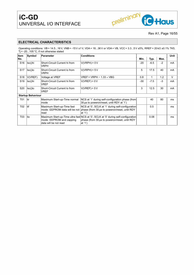
ELECTRICAL CHARACTERISTICS
Operating conditions: VB = 14.5...16 V, VNB = -15 V ±1 V, VDA = 18...36 V or VDA = VB, VCC = 3.3...5 V ±5%, RREF = 20 kΩ ±0.1% TK5,Tj = -20...105 °C, if not otherwise statedItem Symbol Parameter Conditions UnitNo. Min. Typ. Max.
S16 Isc()hi Short-Circuit Current hi fromVRPH
V(VRPH) = 0 V -20 -6.5 -2 mA
S17 Isc()lo Short-Circuit Current lo fromVRPH
V(VRPH) = 5 V 5 17.5 40 mA
S18 V(VREF) Voltage at VREF VREF = VRPH − 1.33 ∗ VBG 0.8 1 1.2 VS19 Isc()hi Short-Circuit Current hi from
VREFV(VREF) = 0 V -30 -7.5 -3 mA
S20 Isc()lo Short-Circuit Current lo fromVREF
V(VREF) = 5 V 3 12.5 30 mA
Startup BehaviourT01 tir Maximum Start-up-Time normal
modeNCS at ’1’ during self-configuration phase (from30µs to poweron/reset, until RDY at ’1’)
40 80 ms
T02 tif Maximum Start-up-Time fastmode: EEPROM data will be notread
NCS at ’0’, SCLK at ’1’ during self-configurationphase (from 30µs to poweron/reset, until RDYat ’1’)
0.5 ms
T03 tix Maximum Start-up-Time ultra fastmode: EEPROM and zappingdata will be not read
NCS at ’0’, SCLK at ’0’ during self-configurationphase (from 30µs to poweron/reset, until RDYat ’1’)
0.08 ms
preliminary
preliminary iC-GDUNIVERSAL I/O INTERFACE
Rev A1, Page 17/55
EXTERNAL CIRCUITRY
uProcessor
ROM
Syst
em B
us
V
TLUT
Counter2x32 bit
PWM Generator2x32 bit
Universal Dual IO-Interface& Test
Digital Filter
iC-GD
EEPR
OM
uCon
trolle
r / F
PGA
do not
5 V Regulator
3.3V
Voltage
VPH/VREF Buffer
Chip temperature- Measurement
Current Output
I/O Channel 1
Monitoring
Clock Generation
Data sync
Start-up
I2C
-15V 15V 24V
connect!
chan
nel 1
chan
nel 2
0.1%
+
low TK
SPI
Bias
Production
- Monitoring
Voltage Output
Push-Pull Driver
Digital Input
Voltage Input
Current Input
U
I
I/O Channel 2
Diagnostics14bit-SAR
TOK2
LED2
UP2
UI2
VPD VCC VB
SYNC1SYNC2
IA1
LED1
UP1
UI1
TEST
GNDPGNDAGNDL
NCSSCLKSDI
NIRQRDYNRES
VREFVPA
RP
CLK
RN
UN1
VDAVNBVRPH
SCLSDA
ADR
CT(7:0)
UN2
IA2
SDO
TOK1
>130
CVPD11nF
CVPD2100nF
+
++-
CVB21μF
CVB1100nF
CVPA100nFCVR
10μFCVCC21μF
CVNB21μF100nF 100nF
CVDA1CVCC1100nF
CVDA2
20K
3.3KRSCL RSDA
3.3K
100nFCVNB1
RREF
VNBREF
REF
VCC VDAVB
C>130
1nFCVPD1
100nFCVPD2
1μFCVB2
100nFCVB1CVNB1
100nF
20KRREF
RSCL3.3K 3.3K
RSDA
CVDA1100nF100nF
CVCC110μFCVDA2
1μFCVCC2
1μFCVNB2CVPA
100nF
CVR100nF
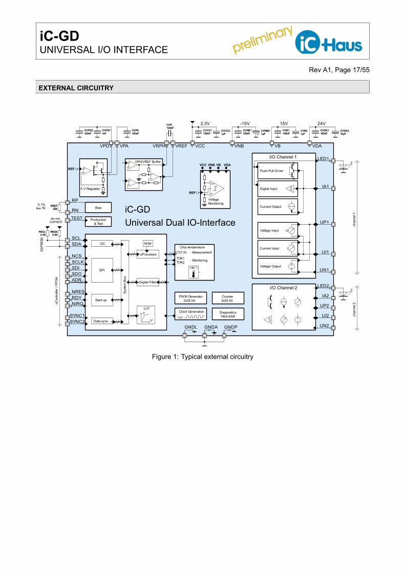
Figure 1: Typical external circuitry
preliminary
preliminary iC-GDUNIVERSAL I/O INTERFACE
Rev A1, Page 18/55
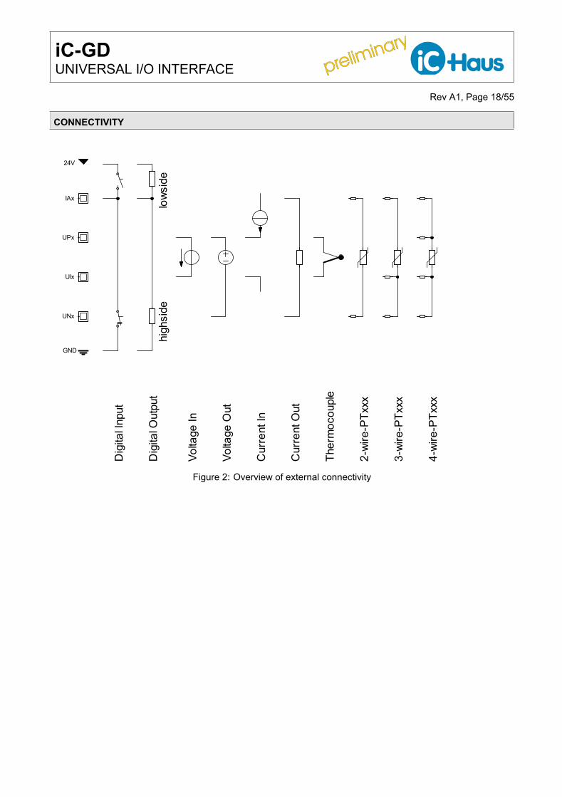
CONNECTIVITY
UNx
Dig
ital I
nput
Dig
ital O
utpu
t
Volta
ge In
Volta
ge O
ut
Cur
rent
In
Cur
rent
Out
2-wi
re-P
Txxx
3-wi
re-P
Txxx
4-wi
re-P
Txxx
Ther
moc
oupl
e
high
side
lows
ide
GND
24V
IAx
UPx
UIx
Figure 2: Overview of external connectivity
preliminary
preliminary iC-GDUNIVERSAL I/O INTERFACE
Rev A1, Page 19/55
FUNCTION DESCRIPTION
Power supplyThe iC is supplied via the following pins:
Power SupplyPin Name Function Range typ. Value
VB positive analog supply 14.5...16 V +15 VVNB negative analog supply -16...-14 V -15 VVCC positive digital supply 3.135...5.25 V 3.3 or 5 VVDA positive power supply 18...36 V 24 V
GNDP power ground 0 V 0 VGNDL logic ground 0 V 0 VGNDA analog ground 0 V 0 V
Table 4: Power Supply
The pins GNDP, GNDL and GNDA are to be connectedexternally via a neutral point.
Default state of IO pins• IAx: Configured as digital type 3 inputs according to
DIN/EN 61131-2• UPx: Configured as voltage outputs with 0 V vs. UNx• UIx: Pulldown current vs. VNB• UNx: Pulldown current vs. GNDDigital inputs IAxFor the digital inputs several pull-down currents accord-ing to DIN/EN61131-2 and a pull-up current can be set.The status of the digital inputs can be indicated viaLEDs to ground at the pins LEDx even if the iC is notsupplied with voltage. In order to reduce power dissi-pation, the pull-down current flows through the LEDs toground. If no LED is used, the corresponding LEDx pinmust be connected to ground.
Digital outputs IAxThe digital outputs can be configured as low-side, high-side or push-pull drivers. If they are not configured asdigital outputs they remain high-impedance.
The outputs are current-limited and switch off when theupper over-temperature limit T2 is reached. When thelower over-temperature limit T1 is exceeded, only thechannel with excessive ouput current is disconnected.
A freewheeling circuit for inductive loads limits the pos-itive voltage versus GNDP and the negative voltageversus VDA.
Diagnostics allow measuring and monitoring the outputcurrent in the output transistors directly. With appro-priately configured pull-up or pulldown currents andvoltage comparators, the status (output on or off, linebreak or short circuit to GNDP or VDA) can be detected.
Analog inputs (UPx, UIx)Table 5 shows the possible measuring ranges. Themaximum ratings marked by (*) only apply, if the chan-nel is configured as plain voltage input (IO_SEL_x = VI).Then the entire range is valid. If the channel is con-figured as temperature sensor (IO_SEL_x = TM), themaximum ratings in table 10 apply. The inputs includecable-break detection. The current inputs are currentlimited to protect the measuring resistor. In addition,it is possible to implement floating voltage or currentmeasurements (e.g. floating thermocouples).
The individual measuring range must be calibrated toreach the specified accuracy. The accuracy accord-ing to the characteristics S02 to S05 is summarized intable 6.
preliminary
preliminary iC-GDUNIVERSAL I/O INTERFACE
Rev A1, Page 20/55
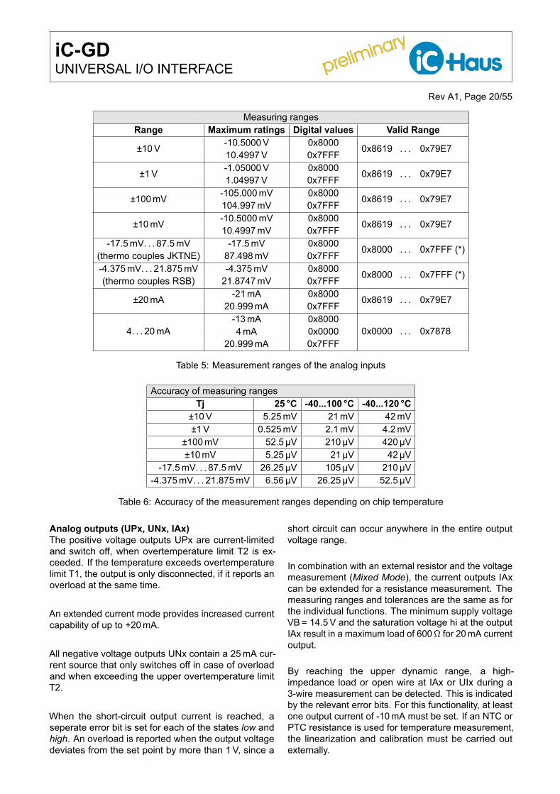
Measuring rangesRange Maximum ratings Digital values Valid Range
±10 V -10.5000 V 0x8000 0x8619 . . . 0x79E710.4997 V 0x7FFF
±1 V -1.05000 V 0x8000 0x8619 . . . 0x79E71.04997 V 0x7FFF
±100 mV -105.000 mV 0x8000 0x8619 . . . 0x79E7104.997 mV 0x7FFF
±10 mV -10.5000 mV 0x8000 0x8619 . . . 0x79E710.4997 mV 0x7FFF
-17.5 mV. . . 87.5 mV -17.5 mV 0x8000 0x8000 . . . 0x7FFF (*)(thermo couples JKTNE) 87.498 mV 0x7FFF-4.375 mV. . . 21.875 mV -4.375 mV 0x8000 0x8000 . . . 0x7FFF (*)(thermo couples RSB) 21.8747 mV 0x7FFF
±20 mA -21 mA 0x8000 0x8619 . . . 0x79E720.999 mA 0x7FFF
4. . . 20 mA-13 mA 0x8000
0x0000 . . . 0x78784 mA 0x000020.999 mA 0x7FFF
Table 5: Measurement ranges of the analog inputs
Accuracy of measuring rangesTj 25 °C -40...100 °C -40...120 °C
±10 V 5.25 mV 21 mV 42 mV±1 V 0.525 mV 2.1 mV 4.2 mV
±100 mV 52.5µV 210µV 420µV±10 mV 5.25µV 21µV 42µV
-17.5 mV. . . 87.5 mV 26.25µV 105µV 210µV-4.375 mV. . . 21.875 mV 6.56µV 26.25µV 52.5µV
Table 6: Accuracy of the measurement ranges depending on chip temperature
Analog outputs (UPx, UNx, IAx)The positive voltage outputs UPx are current-limitedand switch off, when overtemperature limit T2 is ex-ceeded. If the temperature exceeds overtemperaturelimit T1, the output is only disconnected, if it reports anoverload at the same time.
An extended current mode provides increased currentcapability of up to +20 mA.
All negative voltage outputs UNx contain a 25 mA cur-rent source that only switches off in case of overloadand when exceeding the upper overtemperature limitT2.
When the short-circuit output current is reached, aseperate error bit is set for each of the states low andhigh. An overload is reported when the output voltagedeviates from the set point by more than 1 V, since a
short circuit can occur anywhere in the entire outputvoltage range.
In combination with an external resistor and the voltagemeasurement (Mixed Mode), the current outputs IAxcan be extended for a resistance measurement. Themeasuring ranges and tolerances are the same as forthe individual functions. The minimum supply voltageVB = 14.5 V and the saturation voltage hi at the outputIAx result in a maximum load of 600Ω for 20 mA currentoutput.
By reaching the upper dynamic range, a high-impedance load or open wire at IAx or UIx during a3-wire measurement can be detected. This is indicatedby the relevant error bits. For this functionality, at leastone output current of -10 mA must be set. If an NTC orPTC resistance is used for temperature measurement,the linearization and calibration must be carried outexternally.
preliminary
preliminary iC-GDUNIVERSAL I/O INTERFACE
Rev A1, Page 21/55
Both voltage and current outputs must be calibratedto reach the specified accuracy. The accuracy accord-ing to the characteristics O02 to O05 is summarized intable 8.
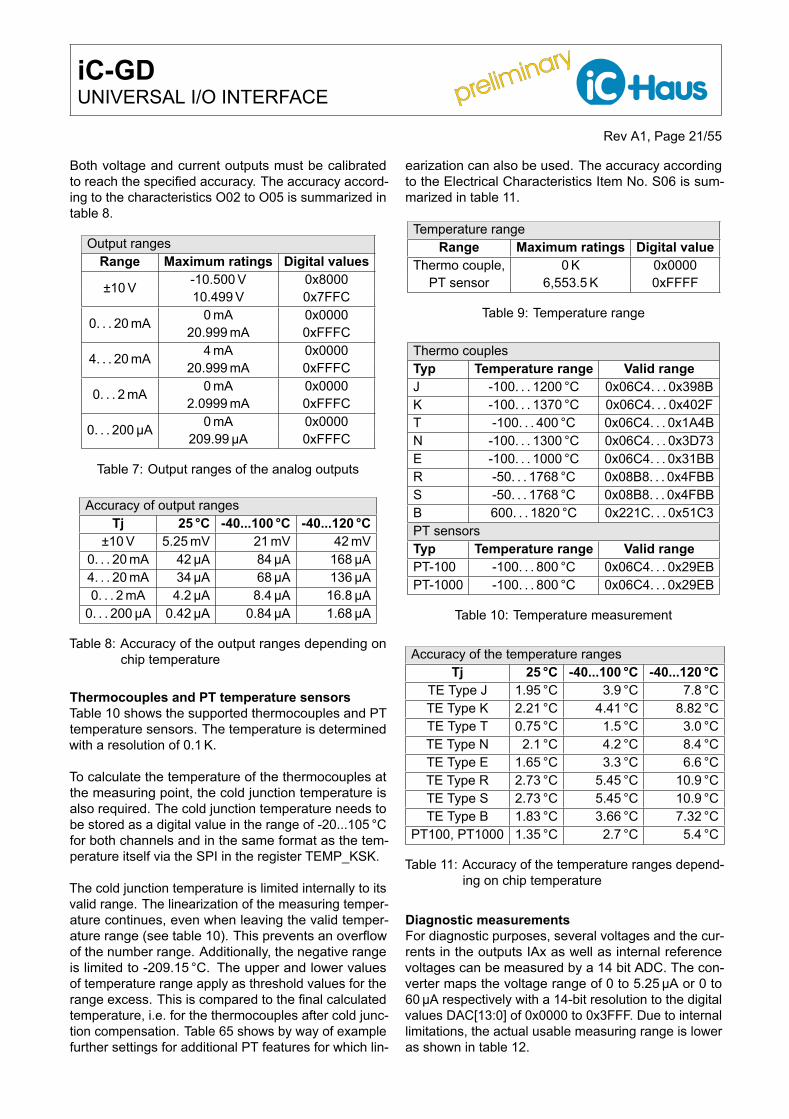
Output rangesRange Maximum ratings Digital values
±10 V -10.500 V 0x800010.499 V 0x7FFC
0. . . 20 mA 0 mA 0x000020.999 mA 0xFFFC
4. . . 20 mA 4 mA 0x000020.999 mA 0xFFFC
0. . . 2 mA 0 mA 0x00002.0999 mA 0xFFFC
0. . . 200µA 0 mA 0x0000209.99µA 0xFFFC
Table 7: Output ranges of the analog outputs
Accuracy of output rangesTj 25 °C -40...100 °C -40...120 °C
±10 V 5.25 mV 21 mV 42 mV0. . . 20 mA 42µA 84µA 168µA4. . . 20 mA 34µA 68µA 136µA0. . . 2 mA 4.2µA 8.4µA 16.8µA
0. . . 200µA 0.42µA 0.84µA 1.68µA
Table 8: Accuracy of the output ranges depending onchip temperature
Thermocouples and PT temperature sensorsTable 10 shows the supported thermocouples and PTtemperature sensors. The temperature is determinedwith a resolution of 0.1 K.
To calculate the temperature of the thermocouples atthe measuring point, the cold junction temperature isalso required. The cold junction temperature needs tobe stored as a digital value in the range of -20...105 °Cfor both channels and in the same format as the tem-perature itself via the SPI in the register TEMP_KSK.
The cold junction temperature is limited internally to itsvalid range. The linearization of the measuring temper-ature continues, even when leaving the valid temper-ature range (see table 10). This prevents an overflowof the number range. Additionally, the negative rangeis limited to -209.15 °C. The upper and lower valuesof temperature range apply as threshold values for therange excess. This is compared to the final calculatedtemperature, i.e. for the thermocouples after cold junc-tion compensation. Table 65 shows by way of examplefurther settings for additional PT features for which lin-
earization can also be used. The accuracy accordingto the Electrical Characteristics Item No. S06 is sum-marized in table 11.
Temperature rangeRange Maximum ratings Digital value
Thermo couple, 0 K 0x0000PT sensor 6,553.5 K 0xFFFF
Table 9: Temperature range
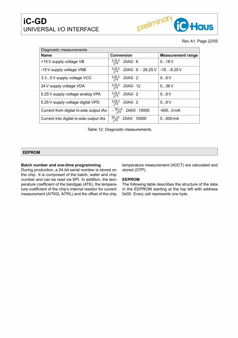
Thermo couplesTyp Temperature range Valid rangeJ -100. . . 1200 °C 0x06C4. . . 0x398BK -100. . . 1370 °C 0x06C4. . . 0x402FT -100. . . 400 °C 0x06C4. . . 0x1A4BN -100. . . 1300 °C 0x06C4. . . 0x3D73E -100. . . 1000 °C 0x06C4. . . 0x31BBR -50. . . 1768 °C 0x08B8. . . 0x4FBBS -50. . . 1768 °C 0x08B8. . . 0x4FBBB 600. . . 1820 °C 0x221C. . . 0x51C3PT sensorsTyp Temperature range Valid rangePT-100 -100. . . 800 °C 0x06C4. . . 0x29EBPT-1000 -100. . . 800 °C 0x06C4. . . 0x29EB
Table 10: Temperature measurement
Accuracy of the temperature rangesTj 25 °C -40...100 °C -40...120 °C
TE Type J 1.95 °C 3.9 °C 7.8 °CTE Type K 2.21 °C 4.41 °C 8.82 °CTE Type T 0.75 °C 1.5 °C 3.0 °CTE Type N 2.1 °C 4.2 °C 8.4 °CTE Type E 1.65 °C 3.3 °C 6.6 °CTE Type R 2.73 °C 5.45 °C 10.9 °CTE Type S 2.73 °C 5.45 °C 10.9 °CTE Type B 1.83 °C 3.66 °C 7.32 °C
PT100, PT1000 1.35 °C 2.7 °C 5.4 °C
Table 11: Accuracy of the temperature ranges depend-ing on chip temperature
Diagnostic measurementsFor diagnostic purposes, several voltages and the cur-rents in the outputs IAx as well as internal referencevoltages can be measured by a 14 bit ADC. The con-verter maps the voltage range of 0 to 5.25µA or 0 to60µA respectively with a 14-bit resolution to the digitalvalues DAC[13:0] of 0x0000 to 0x3FFF. Due to internallimitations, the actual usable measuring range is loweras shown in table 12.
preliminary
preliminary iC-GDUNIVERSAL I/O INTERFACE
Rev A1, Page 22/55
Diagnostic measurementsName Conversion Measurement range+15 V supply voltage VB 5.25 V
214 · DIAG · 6 0...18 V
-15 V supply voltage VNB 5.25 V214 · DIAG · 6 − 26.25 V -18...-8.25 V
3.3...5 V supply voltage VCC 5.25 V214 · DIAG · 2 0...6 V
24 V supply voltage VDA 5.25 V214 · DIAG · 12 0...36 V
5.25 V supply voltage analog VPA 5.25 V214 · DIAG · 2 0...6 V
5.25 V supply voltage digital VPD 5.25 V214 · DIAG · 2 0...6 V
Current from digital hi-side output IAx − 60 µA214 · DIAG · 10000 -600...0 mA
Current into digital lo-side output IAx 60 µA214 · DIAG · 10000 0...600 mA
Table 12: Diagnostic measurements
EEPROM
Batch number and one-time programmingDuring production, a 24-bit serial number is stored onthe chip. It is composed of the batch, wafer and chipnumber and can be read via SPI. In addition, the tem-perature coefficient of the bandgap (ATK), the tempera-ture coefficient of the chip’s internal resistor for currentmeasurement (AITKQ, AITKL) and the offset of the chip
temperature measurement (AOCT) are calculated andstored (OTP).
EEPROMThe following table describes the structure of the datain the EEPROM starting at the top left with address0x00. Every cell represents one byte.
preliminary
preliminary iC-GDUNIVERSAL I/O INTERFACE
Rev A1, Page 23/55
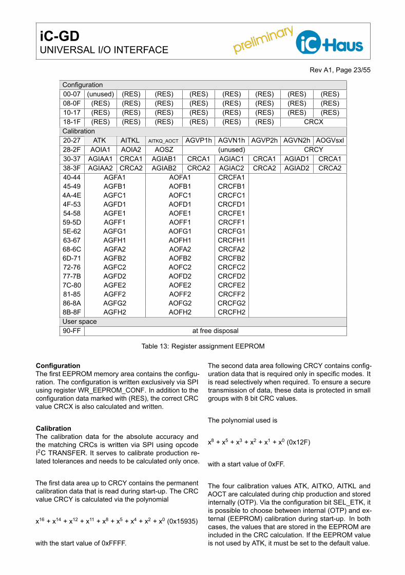
Configuration00-07 (unused) (RES) (RES) (RES) (RES) (RES) (RES) (RES)08-0F (RES) (RES) (RES) (RES) (RES) (RES) (RES) (RES)10-17 (RES) (RES) (RES) (RES) (RES) (RES) (RES) (RES)18-1F (RES) (RES) (RES) (RES) (RES) (RES) CRCXCalibration20-27 ATK AITKL AITKQ_AOCT AGVP1h AGVN1h AGVP2h AGVN2h AOGVsxl28-2F AOIA1 AOIA2 AOSZ (unused) CRCY30-37 AGIAA1 CRCA1 AGIAB1 CRCA1 AGIAC1 CRCA1 AGIAD1 CRCA138-3F AGIAA2 CRCA2 AGIAB2 CRCA2 AGIAC2 CRCA2 AGIAD2 CRCA240-44 AGFA1 AOFA1 CRCFA145-49 AGFB1 AOFB1 CRCFB14A-4E AGFC1 AOFC1 CRCFC14F-53 AGFD1 AOFD1 CRCFD154-58 AGFE1 AOFE1 CRCFE159-5D AGFF1 AOFF1 CRCFF15E-62 AGFG1 AOFG1 CRCFG163-67 AGFH1 AOFH1 CRCFH168-6C AGFA2 AOFA2 CRCFA26D-71 AGFB2 AOFB2 CRCFB272-76 AGFC2 AOFC2 CRCFC277-7B AGFD2 AOFD2 CRCFD27C-80 AGFE2 AOFE2 CRCFE281-85 AGFF2 AOFF2 CRCFF286-8A AGFG2 AOFG2 CRCFG28B-8F AGFH2 AOFH2 CRCFH2User space90-FF at free disposal
Table 13: Register assignment EEPROM
ConfigurationThe first EEPROM memory area contains the configu-ration. The configuration is written exclusively via SPIusing register WR_EEPROM_CONF. In addition to theconfiguration data marked with (RES), the correct CRCvalue CRCX is also calculated and written.
CalibrationThe calibration data for the absolute accuracy andthe matching CRCs is written via SPI using opcodeI2C TRANSFER. It serves to calibrate production re-lated tolerances and needs to be calculated only once.
The first data area up to CRCY contains the permanentcalibration data that is read during start-up. The CRCvalue CRCY is calculated via the polynomial
x16 + x14 + x12 + x11 + x8 + x5 + x4 + x2 + x0 (0x15935)
with the start value of 0xFFFF.
The second data area following CRCY contains config-uration data that is required only in specific modes. Itis read selectively when required. To ensure a securetransmission of data, these data is protected in smallgroups with 8 bit CRC values.
The polynomial used is
x8 + x5 + x3 + x2 + x1 + x0 (0x12F)
with a start value of 0xFF.
The four calibration values ATK, AITKO, AITKL andAOCT are calculated during chip production and storedinternally (OTP). Via the configuration bit SEL_ETK, itis possible to choose between internal (OTP) and ex-ternal (EEPROM) calibration during start-up. In bothcases, the values that are stored in the EEPROM areincluded in the CRC calculation. If the EEPROM valueis not used by ATK, it must be set to the default value.
preliminary
preliminary iC-GDUNIVERSAL I/O INTERFACE
Rev A1, Page 24/55
Description of the data in the EEPROMIn the register AOGVsxl, the LSBs of each 9 bit registerAGVP1, AGVN1, AGVP2, and AGVN2 are organizedas follows:
AGVP1 = AGVP1h & Bit3 (AOGVsxl)AGVN1 = AGVN1h & Bit2 (AOGVsxl)AGVP2 = AGVP2h & Bit1 (AOGVsxl)AGVN2 = AGVN2h & Bit0 (AOGVsxl)
In addition, the register AOGVsxl contains the registerAOV as follows:
AOV = Bit6:4 (AOGVsxl)
The register AITKQ_AOCT is divided as follows:
AITKQ = Bit7:5 (AITKQ_AOCT)AOCT = Bit4:0 (AITKQ_AOCT)
Description mA Current output 0...20 mAB Current output 4...20 mAC Current output 0...2.0 mA (= PT100)D Current output 0...200µA (= PT1000)
Table 14: Description m (Tab. 16)
Description nA Voltage input ±10 VB Voltage input ±1 VC Voltage input ±100 mVD Voltage input ±10m VE Voltage input -17.5...87.5 mVF Voltage input -4.375...21.875 mVG Current input -20...20 mAH Current input 4...20 mA
Table 15: Description n (Tab. 16)
preliminary
preliminary iC-GDUNIVERSAL I/O INTERFACE
Rev A1, Page 25/55
Name Description Default value Digit Interpretation/correction faktorATK Bandgap temperature coef-
ficient0x40 unsigned 1 LSB ≈ -0.6...-0.2 mV (non-linear)
AITKL,AITKQ
Current measurement (lin-ear, square) temperaturecoefficients
0x00 unsigned1 + AITKL ∗ CHIP_TEMP
218
−AITKQ ∗ CHIP_TEMP2
222
AOCT Chip temperature offset 0b00000 signed (2 K) 1 LSB = 1 KAOSZ Oscillator offset,
left-aligned (i.e. 0xFE inEEPROM)
0x7F Bit 6 = signBit 5:0 = value
1 + AOSZc1
, c1 = 192 for AOSZ ≥ 0
11 − AOSZ
c2
, c2 = 180 for AOSZ < 0
AGVPx Positive voltage outputgain
0x100 unsignedRGRA
+ 0.5RGRA
+ AGVPx29
, RG
RA= 19.2
AGVNx Negative voltage outputgain
0x100 unsignedRGRA
+ 0.5RGRA
+ AGVNx29
, RG
RA= 19.2
AOIAx Current output 4...20 mAoffset
0x80 unsignedRGRA
+ 0.5RGRA
+ AOIAx28
, RG
RA= 15.5
AOV Voltage output offset(valid for CH_1 and CH_2)
0b000 unsigned 1 LSB = 1.28 mV
AGIAmx Current output gain,for m see Tab. 14, minusoffset at 4...20 mA
0x80 unsignedRGRA
+ 0.5RGRA
+ AGIAmx28
, RG
RA= 16.6
AGFnx Voltage/current input gain,for n see Tab. 15
0xDE7A signed (2 K)
X =(
1.5 + AGFnx215
)∗(X ′ + AOFnx
)AOFnx Voltage/current input off-
set,for n see Tab. 15
0x0000 signed (2 K) (see AGFnx)
Table 16: Description of EEPROM data
preliminary
preliminary iC-GDUNIVERSAL I/O INTERFACE
Rev A1, Page 26/55
CALIBRATION
BandgapThe adjustable on-chip, second-order temperature-com-pensated bandgap is the voltage reference of the iC-GD.For adjusting the voltage reference, the parameter withthe lowest temperature coefficient is calculated. Thisvalue is calculated during the production process andstored on-chip (OTP). It can be overwritten by a valuestored in the external EEPROM. A bandgap voltagevoltage that is too low is indicated in the supervisoryregister SPV_INT.
BiasThe reference current of the iC-GD is generated byan external resistor, RREF, between the pins RP andRN. To achieve a high accuracy of the current out-puts, a resistor with a low temperature coefficient isrequired. The absolute value is not critical, but mustnot exceed ±1% to remain within the calibration rangeof the current outputs. The current in the resistor ismonitored and the status is indicated in the supervisoryregister SPV_REG. When leaving the tolerance range,it switches to an on-chip generated current. To preventvoltage drop on the supply line and bond wire at pin RN,this pin must not be connected externally to ground.
ClockAn adjustable, internal oscillator generates a 2 MHzclock with a low temperature coefficient. A PLL multi-plies this by the factor of 8 for use as the µC system
clock. This PLL is also monitored and its status sig-nalled in the supervisory register SPV_INT.
CalibrationThe required calibration values can be transferred tothe iC-GD in two different ways:
1. The calibration values are written via I2C directlyinto the EEPROM. These changes are not directlytransfered to the chip and require a restart (chang-ing the mode will only be sufficed for calibrationdata that is reloaded selectively on demand i.e.AGIAmx, AGFnx, AOFnx).
2. The calibration values are written directly into theon-chip registers via SPI. Since these registersare not accessible in regular operation, the cali-bration mode must be activated. After all requiredcalibration data have been calculated, they arealso written into the EEPROM.
Calibration mode is activated by the registerSPI_LOCK_RESET. If calibration mode is active, theinternal register addresses used for the SPI communi-cation differ partly from the valid addresses. If registersother than the calibration registers must be used, cali-bration mode must be deactivated again by the registerSPI_LOCK_RESET. The remaining opcodes, includingthose for the transmission of process data, remain fullyfunctional. Table 17 shows the valid internal addressesfor calibration mode.
preliminary
preliminary iC-GDUNIVERSAL I/O INTERFACE
Rev A1, Page 27/55
Name Internal address Hints and further settingsATK 0x2CAITKL 0x69AITKQ, AOCT 0x7F AITKQ: bits(7:5), AOCT: bits(4:0)AOSZ 0x68 Requires a waiting time of 200µs after writingAGVP1h 0x28AGVN1h 0x29AGVP2h 0x2AAGVN2h 0x2BAGVsxl 0x1FAOIA1 0x1EAOIA2 0x2FAGIAm1 0x1DAGIAm2 0x2EAGFn1 0x0E – 0x0F REG(0x0C) = 0x5C, REG(0x3A) = 0xFF (*)AGFn2 0x0E – 0x0F REG(0x0C) = 0x5D, REG(0x3A) = 0xFF (*)AOFn1 0x0E – 0x0F REG(0x0C) = 0x5E, REG(0x3A) = 0xFF (*)AOFn2 0x0E – 0x0F REG(0x0C) = 0x5F, REG(0x3A) = 0xFF (*)
Table 17: Internal calibration register addresses
(*) The order is relevant. First, the date, then the fur-ther settings in order as shown in table 15 must be set.Register 0x3A acts as trigger.
ATK – Bandgap TKAOCT – Chip temperature measurement offsetAITKQ, AITKL – Current measurement resistor TKThe calibration of the bandgap, the chip temperatureand the current- measurement resistor is performedduring chip-production. The values are stored on-chip(OTP). A read access is possible via the register tableaccording to table 17.
AOSZ oscillatorThe calibration of the oscillator is done via the registerAOSZ(6:0) in the range of approx. ±31.5% with a res-olution of approx. 0.5%. To this end, a divided integerfrequency of the internal clock (PWM) can either beoutput at the digital output IA1 or at pin SYNC1.
For output at IA1, the counter can be used in PWMmode. The output at the SYNC1 pin requires an ad-ditional command according to table 18. It shows theoutput of a 10 kHz signal at pin SYNC1 by way of ex-ample. Determined by the system, the first period isapprox. 80 ns shorter when output at pin SYNC1.
The oscillator must not be operated over its nominal fre-quency, since this can crash the internal µC and causedata errors. Thus during start-up, the lowest possiblefrequency is used. When reading the frequency fromthe EEPROM after start-up, the value is only acceptedif the respective CRC is correct.
There are no limitations for the calibration mode. Forcalibration, two iterations of the following equationwith a start value of AOSZ0 = -63 are usually required.Based on AOSZn and fmess, the respective valid equa-tion must be selected (4 cases).
Attention should be paid to the format of AOSZ accord-ing to table 16 which does not represent a two’s com-plement value. The start value corresponds to 0xFE(left-aligned, LSB unused, MSB = sign, remainder =value) in the EEPROM.
Command EffectBX 00 06 IO_SEL_1P = CNTBX 01 43 SYNC_SEL_1 = DISOBX 03 31 Counter value 1 = PWM in HS
modeDX 28 03200190 Tges = 100µs, Thigh = 50µs0X 80 PROCESS DATA 1 = ’1’ (PWM
on)
For additional output via SYNC1 only:BX 39 AA Activate calibration modeBX 25 80 Start output PWM → SYNC1
* Measurement *BX 25 00 Stop output PWM → SYNC1BX 39 A5 Deactivate calibration mode
Table 18: Calibration AOSZ
preliminary
preliminary iC-GDUNIVERSAL I/O INTERFACE
Rev A1, Page 28/55
Case 1: AOSZn ≥ 0, AOSZn ≥ c1 ∗(
fmeasfset
− 1)
AOSZn+1 = AOSZn ∗f set
f meas+ c1 ∗
(f set
f meas− 1)
Case 2: AOSZn ≥ 0, AOSZn < c1 ∗(
fmeasfset
− 1)
AOSZn+1 =
1 − f meas
f set∗ 1
1 + AOSZnc1
∗ c2
Case 3: AOSZn < 0, AOSZn ≥ c2 ∗(
1 − fsetfmeas
)AOSZn+1 =
f set
f meas∗ 1
1 − AOSZnc2
− 1
∗ c1
Case 4: AOSZn < 0, AOSZn < c2 ∗(
1 − fsetfmeas
)AOSZn+1 = AOSZn ∗
f meas
f set+ c2 ∗
(1 − f meas
f set
)
withc1 = 192, c2 = 180
AOV – Voltage output offsetThe output voltage offset calibration, UPx − UNx, isdone for both channels via the 3-bit register AOV.The calibration range covers approx. 9 mV in stepsof 1.28 mV.
With AOV = 0b000 at channel 1, a voltage of 0 mV(0x0000) is output and the (negative) offset is deter-mined. The calibration value AOV then results in:
AOV = − Vmeas
1.28 mV
AGVsx – Voltage output gainThe output voltage gain calibration, UPx − UNx, iscentrally carried out via the internal 5.25 V voltage ref-erence of the 14-bit D/A converter. The calibrationrange based on the output voltage of ±10.5 V is approx.512 mV in steps of approx. 1 mV.
For this, a previous calibration of the offset (AOV) isrequired.
The four calibration values AGVPx(8:0) andAGVNx(8:0) must be calculated for both channels andseparately for the positive and negative output range.For start value AGVsx0 = 0x100 and the maximummagnitude of voltage Vset must be performed:
AGVsxn+1 = AGVsxn ∗Vmeas
Vset+29 ∗19.2∗
(Vmeas
Vset− 1)
AOIAx – Current output offsetThe current output offset applies to the 4 to 20 mA rangeonly. The calibration range is approx. 0.25 mA. Thecalibration steps are approx. 1µA.
The calibration is performed with IAx at 4 mA (0x0000)via AOIAx(7:0). For this, two iterations according to thefollowing equation with the start value AOIAx0 = 0x80are performed:
AOIAxn+1 = AOIAxn ∗Imeas
Iset+ 28 ∗ 15.5 ∗
(Imeas
Iset− 1)
AGIAmx – Current output gainThe calibration range for the current output gain is ap-prox. 6.1% (minus offset of the 4 to 20 mA range). Thecalibration steps are 1/256 (i.e. e.g. selected in the 0to 20 mA range with 21 mA: calibration range approx.1.28 mA, calibration steps approx. 5µA).
For the calibration of the current output gain, a previouscalibration of the current output offset (AOIAx, only inthe range of 4 to 20 mA) is required.
The output current calibration at IAx is carried out forboth output ranges of 0 to 20 mA as gain of the fullscalevalue of approx. 21 mA (0xFFC) via AGIAAx(7:0) orAGIABx(7:0).
For the ranges 0 to 2 mA or 0 to 200µA, that are primar-ily intended for the PT100 or PT1000 measurement, thegain is calculated at 1.7 mA or 170µA (both 0xCF3C)via AGIACx(7:0) or AGIADx(7:0). This value is used forenergizing the PT elements and is stored on the chip.The calibration is made with in each case 2 iterationsaccording to the following equation with the start valueAGIAmx0 = 0x80:
AGIAmxn+1 = AGIAmxn ∗Imeas−Ioffset
Iset−Ioffset
+28 ∗ 16.6 ∗(
Imeas−IoffsetIset−Ioffset
− 1)
AGFnx, AOFnxThe current/voltage measurement calibration is madefor the different measuring ranges by setting the offset(AOFnx) and the gain (AGFnx). Required is a previoussuccessful calibration of the voltage outputs.
At AGFnx = 0xC000 and AOFnx = 0x000, several volt-age/current values are externally applied (Xset) and
preliminary
preliminary iC-GDUNIVERSAL I/O INTERFACE
Rev A1, Page 29/55
read back via the SPI (Xmeas). The two maximum val-ues are used for all measuring ranges (value 1 and 2).In addition, for the symmetric measuring ranges, the off-set at 0 V/0 mA (value 0) is determined. For the currentmeasurement offset, also the current chip temperatureand the temperature coefficient values AITKQ, AITKLare required. The latter are stored on the chip, see table17. The required values are used unitless in the formatof the process data: Xset und Xmeas as signed numbers,and additionally for the current measurement AITKQ,AITKL and CHIP_TEMP, all as unsigned numbers.
The following four conditions must be kept:(1.5 + AGFnx
215
)∗(AOFnx + 215) > 215 − 1
(1.5 + AGFnx
215
)∗(AOFnx − 215) < −215
(1.5 + AGFnx
215
)∗ AOFnx < 215 − 1
(1.5 + AGFnx
215
)∗ AOFnx > −215
3-point calibration (symmetrical ranges)The following formulae are valid for the ranges ±10 V,±1 V, ±100 mV, ±10 mV, ±20 mA.
Point 0 is calibrated exactly (to use for offset), point 1and point 2 are calibrated best possible. The pointsshould be distributed equidistantly.
ExamplePoint 0: 0 V, point 1: +10 V, point 2: -10 V.
AGFnx =(
Xset 1 − Xset 0
Xmeas 1 − Xmeas 0+ Xset 2 − Xset 0
Xmeas 2 − Xmeas 0− 3)∗ 214
AOFnx(VI) = Xset 0
1.5 + AGFnx215
− Xmeas 0
AOFnx(CI) =
(Xset 0
1.5 + AGFnx215
− Xmeas 0
)∗ 1
f T
2-point calibration (asymmetrical ranges)The following formulae are valid for the ranges -17.5 mVto 87.5 mV, -4.375 mV to 21.875 mV, 4 to 20 mA. Point1 and point 2 are to be adjusted exactly.
ExamplePoint 1: 4 mA, point 2: 20 mA.
AGFnx =(
Xset 2 − Xset 1
Xmeas 2 − Xmeas 1− 1.5
)∗ 215
AOFnx(VI) = Xset 1 ∗ Xmeas 2 − Xset 2 ∗ Xmeas 1
Xset 2 − Xset 1
AOFnx(CI) = Xset 1 ∗ Xmeas 2 − Xset 2 ∗ Xmeas 1 + c0 ∗ (f T − 1) ∗ (Xset 2 − Xset 1 + Xmeas 1 − Xmeas 2)(Xset 2 − Xset 1) ∗ f T
with c0 = 7710, f T = 1 + AITKL ∗ CHIP_TEMP218 − AITKQ ∗ CHIP_TEMP2
222
preliminary
preliminary iC-GDUNIVERSAL I/O INTERFACE
Rev A1, Page 30/55
STARTUP, RESET, WATCHDOGS
When the supply voltages are applied and VCC ex-ceeds the undervoltage reset threshold (Vtu(VCC)hi),the iC-GD starts with the self-configuration. The inter-nal registers are initialized and the configuration andcalibration data from the EEPROM are read. Duringthe phase of self-configuration, (RDY = lo), SPI commu-nication is blocked.
The EEPROM is read via the I2C interface. Here, theconfiguration and calibration data are read from theEEPROM and written into the internal registers. Dur-ing the entire configuration, a 16-bit CRC checksumis calculated and compared with the checksum that isalso stored in the EEPROM. If these do not match, theconfiguration will be rejected and the chip returns toits default state. The error status is stored in registerSPV_REG, bit ST_CONF. Also, a 16-bit checksum iscalculated for the calibration data and compared withthe checksum stored in the EEPROM. If those do notmatch, only the error status is stored in the registerSPV_REG, bit ST_CALIB. The read data is kept, ex-cept for the frequency calibration. Additionally, in cer-tain modes further calibration data from the EEPROM isread and protected by a separate 8-bit CRC if required.
The iC uses the memory area of the EEPROM shownin table 13. The subsequent memory area is freelyavailable to the user.
The chip then provides several possibilities for internaland external resetting. The cause of the last reset isstored in a status register.
• Supply voltage: If the supply voltage VCC dropsbelow the undervoltage reset threshold (Vtu(VCC)lo),the chip is reset. As stated above, it restarts whenthe supply voltage is restored.
• NRES pin: If the NRES pin is low for at least tRESlo,the chip is reset. Shorter pulses may but do not haveto cause a reset.
• Reset via SPI: The chip can be reset immediatelyby writing into the register SPI_LOCK_RESET therelevant command.
• Watchdog SPI: An internal watchdog timer can beoptionally enabled, to monitor the SPI communication.If no valid SPI communication takes place during acertain time period (see table 19), the watchdog re-sets the iC. A valid communication is one of theopcodes "PROCESS DATA 1/2/1 and 2".
• Watchdog µC: An internal watchdog monitors the in-ternal processor. The processor operates the watch-dog regularly during its main routine. If the watchdogis not operated within the the µC time-out (see table19), it resets the iC.
Reset timesWatchdog µC 125 ms ±5 msWatchdog SPI 53 ms ±3 ms
Table 19: Watchdogs (times are only valid with cali-brated oscillator)
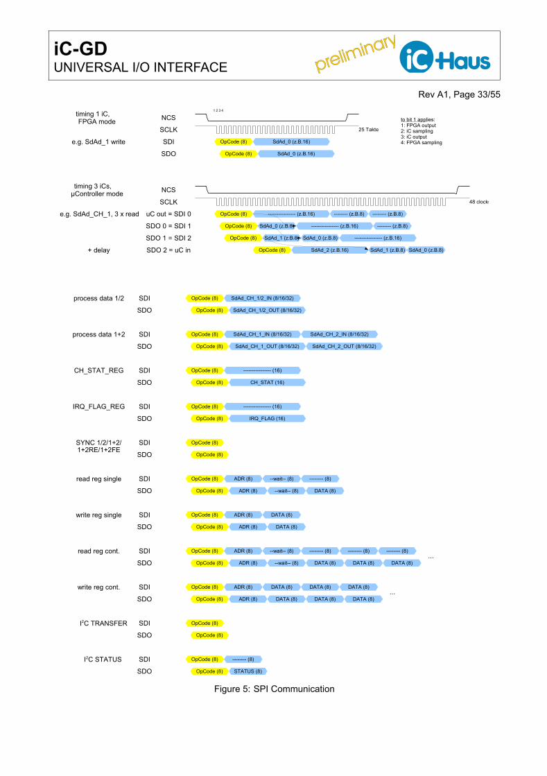
SPI
The iC-GD is controlled via an SPI interface. The SPIinterface allows fast reading of measurement data andthe setting of actuator values as well as reading andwriting of configuration registers. The SPI provides abridge to the I2C interface and thus also to the con-nected EEPROM.
The SPI operates synchronously with the supplied clock.To this end, it samples the input data with the fallingedge and outputs the data with the rising edge. Bydefault, it outputs the input data with half a clock delay.The iC is activated by the NCS pin, so that the subse-quent 8 bits can be interpreted as control code. Thiscontains a 4-bit opcode, a 3-bit address and a broad-cast bit. If the iC as such is not addressed, it hibernatesand only relays the input data. Otherwise, it interpretsthe opcode.
An additional delay in the signal path (SDO) between0 and 7 clocks can be set via the configuration bitEN_UCM. Thus, the total delay of a daisy chain ofup to 8 iCs can be set up to a multiple of 8 clocks. Thishas to be carried out in the last iC of the SPI chain.This iC automatically determines the required numberof clocks of additional delay by means of its address.This allows proper control by a µC.
The SPI protocol is optimized for the transfer of sensorand actuator data. Sensor data is available directly fol-lowing the opcode and can be clocked out subsequently.Actuator data can be sent directly following the opcode.To read data from internal registers, a provisioning timeof 8 clocks following the opcode and the address isrequired, which can be filled with optional data. To writeregister data, no padding is required by the SPI. When
preliminary
preliminary iC-GDUNIVERSAL I/O INTERFACE
Rev A1, Page 31/55
reading and writing data via I2C, e.g. to the EEPROM,one has to poll for the end of this process before a newI2C communication can be started.
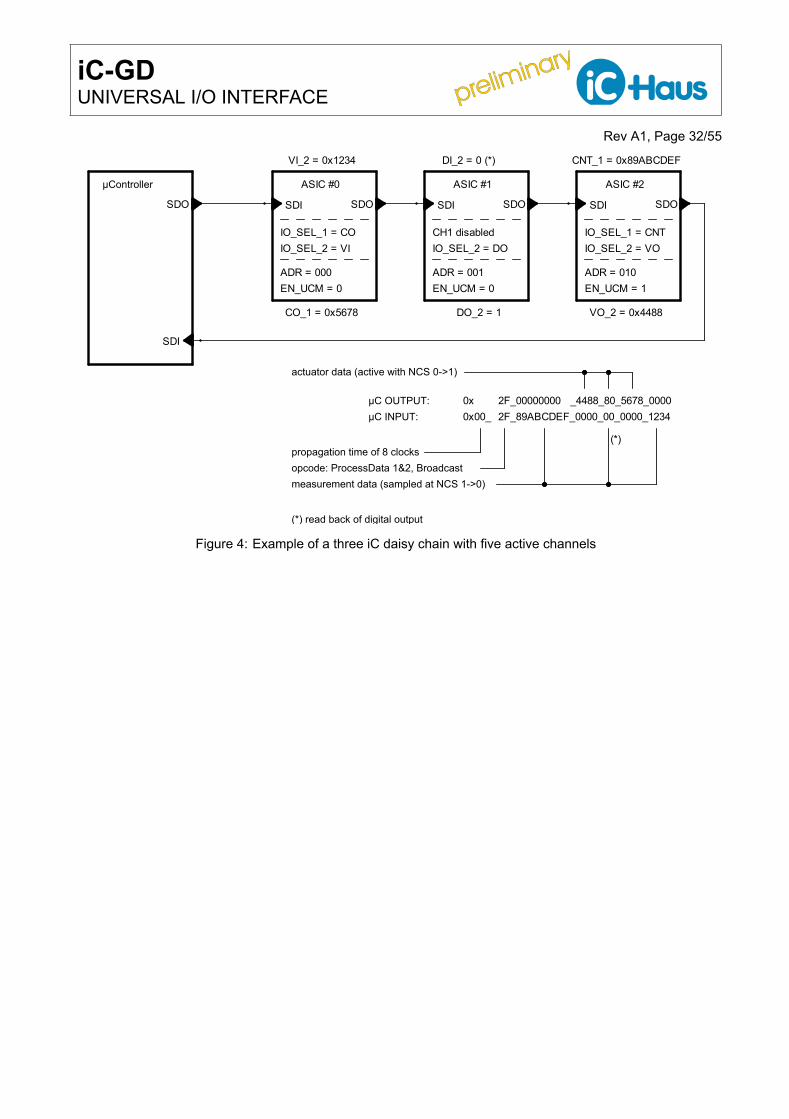
In addition, the SPI provides opcodes as respectiveSYNC signals (edges and channels) and opcodesfor fast reading of the registers CH_STAT_REG andIRQ_FLAG_REG. Figure 5 shows the SPI communica-tion.
The SPI is blocked during the startup (RDY = 0). Nocommunication is possible during this time. In normaloperation, 30µs after the beginning of startup at thelatest (usually with the rising edge of NRES), NCS mustbe high. Otherwise the iC performs a quickstart thatskips reading the EEPROM and the internal calibration
data. In this case, both CRC error bits are set (seechapter Calibration).
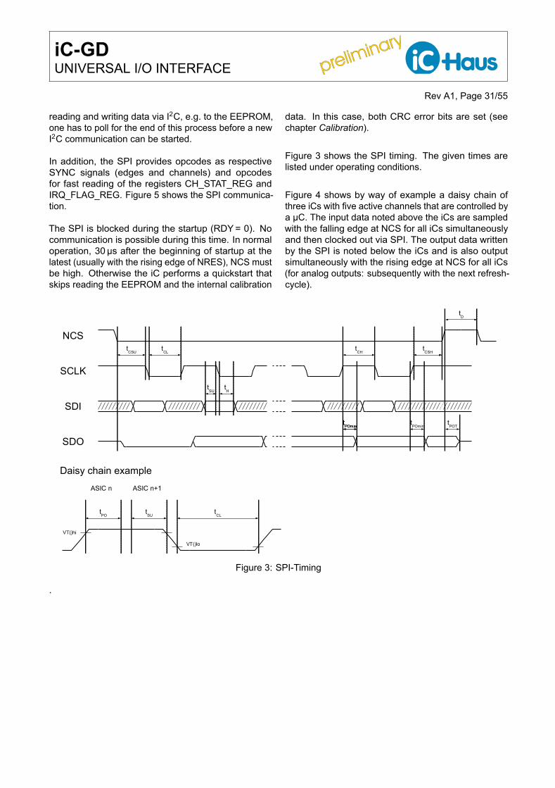
Figure 3 shows the SPI timing. The given times arelisted under operating conditions.
Figure 4 shows by way of example a daisy chain ofthree iCs with five active channels that are controlled bya µC. The input data noted above the iCs are sampledwith the falling edge at NCS for all iCs simultaneouslyand then clocked out via SPI. The output data writtenby the SPI is noted below the iCs and is also outputsimultaneously with the rising edge at NCS for all iCs(for analog outputs: subsequently with the next refresh-cycle).
SCLK
SDI
SDO
NCStCSU
tCL
tCSH
tD
tH
tSU
tPOmax
tPOT
tPOmin
tPOmax
tCL
tPO
tSU
ASIC n ASIC n+1
VT()hi
VT()lo
tCH
Daisy chain example
Figure 3: SPI-Timing
.
preliminary
preliminary iC-GDUNIVERSAL I/O INTERFACE
Rev A1, Page 32/55
UOT
measurementPdataPUsampledPatPNCSP4w9=T
=x
propagationPtimePofP5Pclocks
opcode7PProcessDataP4µAvPBroadcast
µCPINPUT7
µCPOUTPUT7
=x==_
actuatorPdataPUactivePwithPNCSP=w94T
VO_APbP=xEE55
ADRPbP===
EN_UCMPbP=
IO_SEL_APbPVI
IO_SEL_4PbPCO
SDO
SDI
SDO
VI_APbP=x4ARE
CO_4PbP=xML35
ASICP24
ADRPbP==4
EN_UCMPbP=
IO_SEL_APbPDO
CH4Pdisabled
DO_APbP4
ASICP2A
ADRPbP=4=
EN_UCMPbP4
IO_SEL_APbPVO
IO_SEL_4PbPCNT
CNT_4PbP=x56ABCDEF
AF_========P _EE55_5=_ML35_====
AF_56ABCDEF_====_==_====_4ARE
µController
DI_APbP=PUOT
ASICP2=
UOTPreadPbackPofPdigitalPoutput
SDOSDISDOSDI SDI
Figure 4: Example of a three iC daisy chain with five active channels
preliminary
preliminary iC-GDUNIVERSAL I/O INTERFACE
Rev A1, Page 33/55
SCLK
SDI
SDO
NCS
OpCodeHQxF SdAd_wHQzlBlmµF
OpCodeHQxF SdAd_wHQzlBlmµF
processHdataHm-, SDI
SDO
OpCodeHQxF SdAd_CH_m-,_INHQx-mµ-P,F
OpCodeHQxF SdAd_CH_m-,_OUTHQx-mµ-P,F
processHdataHmg, SDI
SDO
OpCodeHQxF SdAd_CH_m_INHQx-mµ-P,F
OpCodeHQxF SdAd_CH_m_OUTHQx-mµ-P,F
CH_STAT_REG SDI
SDO
OpCodeHQxF
OpCodeHQxF
IRQ_FLAG_REG SDI
SDO
OpCodeHQxF
OpCodeHQxF
SYNCHm-,-mg,- SDI
SDO
OpCodeHQxF
OpCodeHQxF
readHregHsingle SDI
SDO
OpCodeHQxF
OpCodeHQxF
ADRHQxF
ADRHQxF
nnwaitnnHQxF
timingHmHiCiFPGAHmode
nnwaitnnHQxF
writeHregHsingle SDI
SDO
OpCodeHQxF
OpCodeHQxF
ADRHQxF
ADRHQxF
DATAHQxF
DATAHQxF
nnnnnnnnHQxF
DATAHQxF
readHregHcontl SDI
SDO
OpCodeHQxF
OpCodeHQxF
ADRHQxF
ADRHQxF
writeHregHcontl SDI
SDO
OpCodeHQxF
OpCodeHQxF
ADRHQxF
ADRHQxF
DATAHQxF
DATAHQxF
nnnnnnnnHQxF
DATAHQxF
nnnnnnnnHQxF
DATAHQxF
nnnnnnnnHQxF
DATAHQxFlll
DATAHQxF
DATAHQxF
DATAHQxF
DATAHQxFlll
I,CHTRANSFER SDI
SDO
OpCodeHQxF
OpCodeHQxF
nnwaitnnHQxF
nnwaitnnHQxF
SCLK
uCHoutH:HSDIHw
NCS
OpCodeHQxF
timingHPHiCsiµControllerHmode
SDOHwH:HSDIHm
OpCodeHQxF
gHdelay
SdAd_mHQzlBlxF
nnnnnnnnHQzlBlxF
SDOHmH:HSDIH,
OpCodeHQxF SdAd_,HQzlBlmµF SdAd_mHQzlBlxF SdAd_wHQzlBlxF
elglHSdAd_mHwrite
elglHSdAd_CH_miHPHxHread OpCodeHQxF nnnnnnnnnnnnnnnnHQzlBlmµF nnnnnnnnHQzlBlxF nnnnnnnnHQzlBlxF
m , P u
,=HTakte
toHbitHmHapplies5m5HFPGAHoutput,5HiCHsamplingP5HiCHoutputu5HFPGAHsampling
SDOH,H:HuCHin
uxHclocks
SdAd_CH_,_INHQx-mµ-P,F
SdAd_CH_,_OUTHQx-mµ-P,F
I,CHSTATUS SDI
SDO
OpCodeHQxF
OpCodeHQxF
nnnnnnnnHQxF
STATUSHQxF
mg,RE-mg,FE
nnnnnnnnnnnnnnnnHQmµF
CH_STATHQmµF
nnnnnnnnnnnnnnnnHQmµF
IRQ_FLAGHQmµF
SdAd_wHQzlBlxF nnnnnnnnnnnnnnnnHQzlBlmµF
SdAd_wHQzlBlxF nnnnnnnnnnnnnnnnHQzlBlmµF
Figure 5: SPI Communication
preliminary
preliminary iC-GDUNIVERSAL I/O INTERFACE
Rev A1, Page 34/55
COUNTER
Via the two digital inputs with their following spike filters,two 32-bit wide counters can be operated. In singlemode, the counters are operated independently. Indual mode (see below), one counter is controlled byboth inputs. The counters can also be used as PWMgenerators.
For each counter, one reference value can be config-ured that sets a status bit and causes an interrupt, whenreached. In addition, a bit can be configured that de-termines whether an interrupt is caused once or everytime the reference value is reached. In the latter case itcan be reset via the register SPI_LOCK_RESET. Thisprevents the setting of a status bit and the triggering ofan interrupt in case the counter fluctuates around thereference value or is at the reference value. The samefunctions are available for the second reference valueand the overflow and underflow of the counter.
The bit CNT_RAR allows the configuration of a counterto be reset when the reference value is reached (resetat reference). The reference value itself is not reachedthough. Additionally, the input signal can be invertedprior to internal processing and the counting direction(up/down) be set in most counter modes.
The counters operate synchronously with the SYNC sig-nal or asynchronously so that the current value is sup-plied. Some modes do not allow external synchroniza-tion because the respective synchronization is carriedout internally. This affects the time measurement andthe synchronization triggered by the second channel.The synchronous mode also allows reading the asyn-chronous (current) counter value by sending a SYNCcommand to the relevant iC via the SPI and reading thevalue as regular sensor data. Tab. 21 gives an overviewof usable configuration bits depending on the selectedmode. ’X’ means ’possible’, ’-’ means ’not possible’ (bitis ignored), ’(-)’ means ’possible but not useful’.
Additionally, the counter allows the generation of apulse-width modulated signal in two different modes.
• Simple PWM: The PWM mode is selected and both16 bit periods t_high and t_ges as in Table 20 andFigure 6 are written to the reference register. ThePWM can be switched on and off via the processdata. When switched on, it re-starts its period with ’1’.In addition, the pulse-width can be changed duringrun-time by writing the lower half of the reference reg-ister. In this case, a period that has already startedinternally is completed and then the new value isadopted. When the cycle time is changed, the current
period is terminated immediately and a new period isstarted.
• PWM with activation pulse: Unlike in simple PWMmode, an activation pulse is generated at startup be-fore the PWM automatically switches to the regularPWM mode. Note: The registers are interpreted dif-ferently than the simple PWM mode (see Figure 6). Achange of the pulse width is not intended in this mode.It is possible though by writing the entire SET_CNTregister with 0x0000 in the upper half. In contrast tothe simple PWM mode, here the period will not becompleted but starts immediately with a new period.When the cycle time is changed, the current period isterminated immediately and a new period is startedwithout a new activation pulse.
In both modes, the PWM mode supports a high-speedmode (HS) with a resolution of 125 ns, a cycle time ofup to 8.192 ms and a low-speed mode (LS) with a res-olution of 16 ns and a cycle time of up to 1.048 s (seeTable 20). The initial pulse may be up to 1 LSB shorterdue to the temporal resolution of the internal clock inlow-speed mode. The reference register can either bewritten completely (4 bytes) or only its low-order part(2 bytes). For simple PWM, the latter complies with achange of t_high. The PWM then is output at IAx (X =1, 2). Time t_ges must not be 0x0000.
These following modes are supported by the counters:
Single mode
• Pulse counter: Counts pulses (= rising edges) of therespective channel.
• Time measurement period: Measures the time be-tween two rising edges. No external sync possiblebecause it is synchronized with the rising edge.
• Time measurement pulse width: Measures thetime that the respective channel is high. No exter-nal sync possible because it is synchronized with thefalling edge.
• Pulse-width modulation: Generates a PWM signalwith a duty cycle depending on REF_CNT_x. TheHigh-time, cycle time and, if necessary, the activationpulse time are configurable (see figure 6).
Dual Mode
• Pulse counter with trigger: Counts pulses on CH_1.CH_2 serves as a trigger to enable the counter valueto be output. The counter value CH_1 is not reset.Since CH_2 performs the function of synchronization,no external sync is possible.
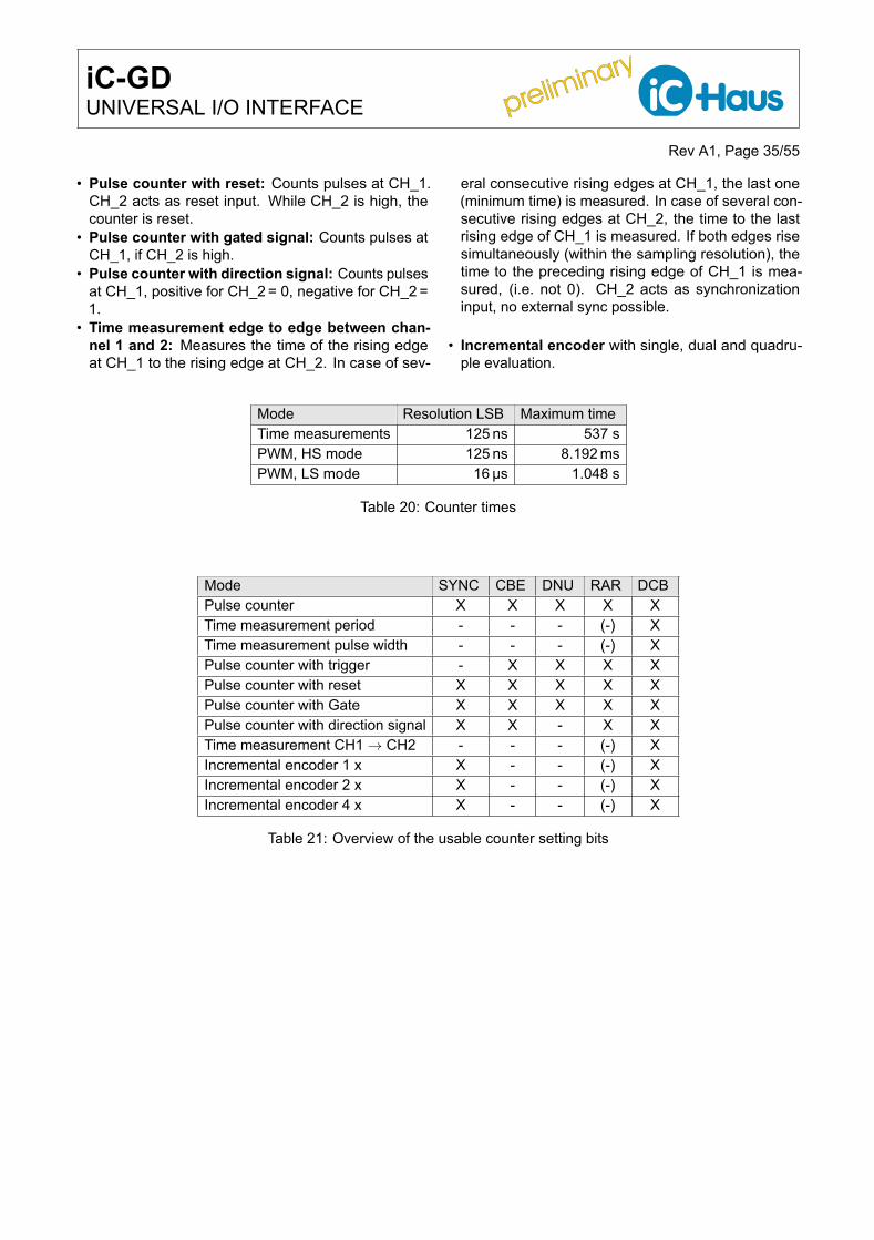
preliminary
preliminary iC-GDUNIVERSAL I/O INTERFACE
Rev A1, Page 35/55
• Pulse counter with reset: Counts pulses at CH_1.CH_2 acts as reset input. While CH_2 is high, thecounter is reset.
• Pulse counter with gated signal: Counts pulses atCH_1, if CH_2 is high.
• Pulse counter with direction signal: Counts pulsesat CH_1, positive for CH_2 = 0, negative for CH_2 =1.
• Time measurement edge to edge between chan-nel 1 and 2: Measures the time of the rising edgeat CH_1 to the rising edge at CH_2. In case of sev-
eral consecutive rising edges at CH_1, the last one(minimum time) is measured. In case of several con-secutive rising edges at CH_2, the time to the lastrising edge of CH_1 is measured. If both edges risesimultaneously (within the sampling resolution), thetime to the preceding rising edge of CH_1 is mea-sured, (i.e. not 0). CH_2 acts as synchronizationinput, no external sync possible.
• Incremental encoder with single, dual and quadru-ple evaluation.
Mode Resolution LSB Maximum timeTime measurements 125 ns 537 sPWM, HS mode 125 ns 8.192 msPWM, LS mode 16µs 1.048 s
Table 20: Counter times
Mode SYNC CBE DNU RAR DCBPulse counter X X X X XTime measurement period - - - (-) XTime measurement pulse width - - - (-) XPulse counter with trigger - X X X XPulse counter with reset X X X X XPulse counter with Gate X X X X XPulse counter with direction signal X X - X XTime measurement CH1 → CH2 - - - (-) XIncremental encoder 1 x X - - (-) XIncremental encoder 2 x X - - (-) XIncremental encoder 4 x X - - (-) X
Table 21: Overview of the usable counter setting bits
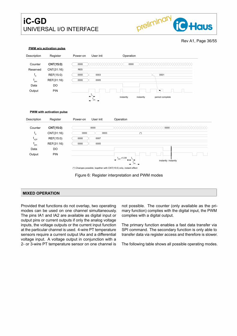
preliminary
preliminary iC-GDUNIVERSAL I/O INTERFACE
Rev A1, Page 36/55
BBBB
lmy
BBBB
RES
CNTlh5:By
CNTl,h:h6y
REFlh5:By
REFl,h:h6y
Counter
Reserved
tH
tges
RegisterDescription Power7on UserPinit Operation
BBBB
BBBB
BBBB
BBB,
BBB5
DO
PIN
BBBh
CNTlh5:By
instantly instantly periodPcomplete
Data
Output
PWM w/o activation pulse
CNTlh5:By
CNTl,h:h6y
REFlh5:By
REFl,h:h6y
Counter
tAZP
tges
RegisterDescription Power7on UserPinit Operation
BBBB
BBBB
BBB7
BBB5
DO
PIN
CNTlh5:By
instantly
Data
Output
PWM with activation pulse
tH
BBBB BBB,
BBBB
tAZP
±hLSB tH
tges
lmyPChangesPpossibleZPtogetherPwithPCNTlh5:ByPonlyZPinstantPeffect
instantly
tH
tges
Figure 6: Register interpretation and PWM modes
MIXED OPERATION
Provided that functions do not overlap, two operatingmodes can be used on one channel simultaneously.The pins IA1 and IA2 are available as digital input oroutput pins or current outputs if only the analog voltageinputs, the voltage outputs or the current input functionat the particular channel is used. 4-wire PT temperaturesensors require a current output IAx and a differentialvoltage input. A voltage output in conjunction with a2- or 3-wire PT temperature sensor on one channel is
not possible. The counter (only available as the pri-mary function) complies with the digital input, the PWMcomplies with a digital output.
The primary function enables a fast data transfer viaSPI command. The secondary function is only able totransfer data via register access and therefore is slower.
The following table shows all possible operating modes.
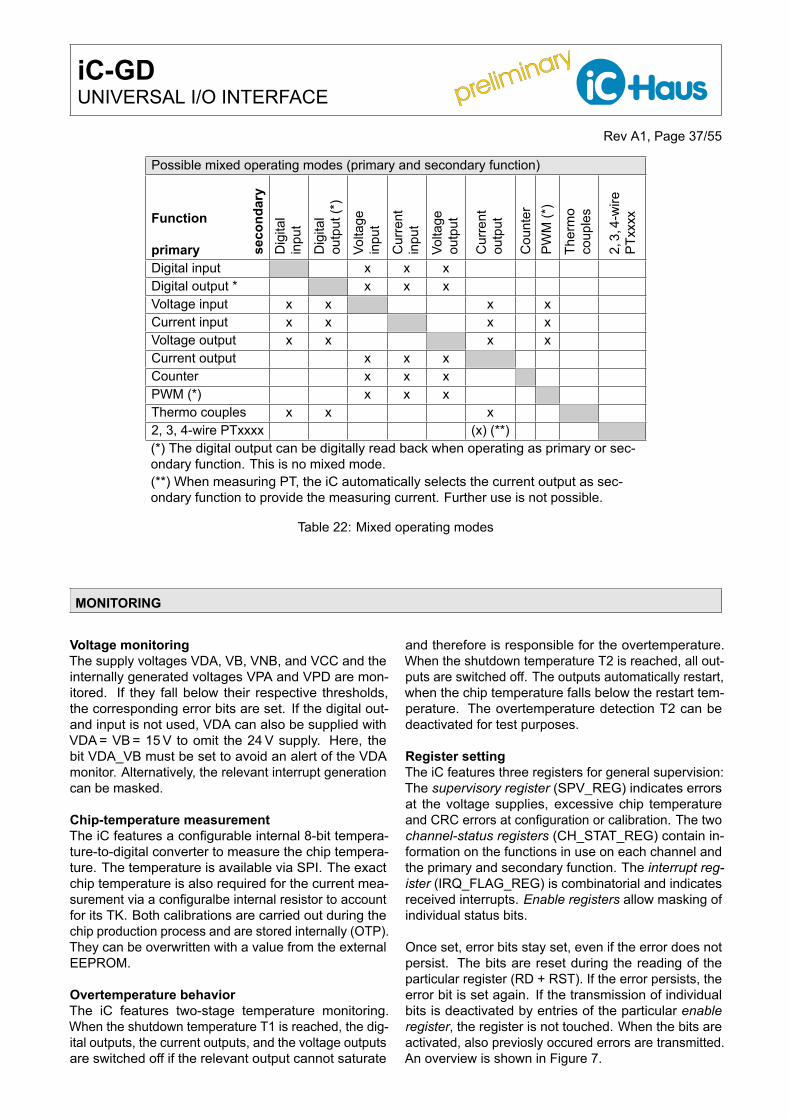
preliminary
preliminary iC-GDUNIVERSAL I/O INTERFACE
Rev A1, Page 37/55
Possible mixed operating modes (primary and secondary function)
Function
primary seco
ndar
yD
igita
lin
put
Dig
ital
outp
ut(*
)
Volta
gein
put
Cur
rent
inpu
t
Volta
geou
tput
Cur
rent
outp
ut
Cou
nter
PWM
(*)
Ther
mo
coup
les
2,3,
4-w
irePT
xxxx
Digital input x x xDigital output * x x xVoltage input x x x xCurrent input x x x xVoltage output x x x xCurrent output x x xCounter x x xPWM (*) x x xThermo couples x x x2, 3, 4-wire PTxxxx (x) (**)(*) The digital output can be digitally read back when operating as primary or sec-ondary function. This is no mixed mode.(**) When measuring PT, the iC automatically selects the current output as sec-ondary function to provide the measuring current. Further use is not possible.
Table 22: Mixed operating modes
MONITORING
Voltage monitoringThe supply voltages VDA, VB, VNB, and VCC and theinternally generated voltages VPA and VPD are mon-itored. If they fall below their respective thresholds,the corresponding error bits are set. If the digital out-and input is not used, VDA can also be supplied withVDA = VB = 15 V to omit the 24 V supply. Here, thebit VDA_VB must be set to avoid an alert of the VDAmonitor. Alternatively, the relevant interrupt generationcan be masked.
Chip-temperature measurementThe iC features a configurable internal 8-bit tempera-ture-to-digital converter to measure the chip tempera-ture. The temperature is available via SPI. The exactchip temperature is also required for the current mea-surement via a configuralbe internal resistor to accountfor its TK. Both calibrations are carried out during thechip production process and are stored internally (OTP).They can be overwritten with a value from the externalEEPROM.
Overtemperature behaviorThe iC features two-stage temperature monitoring.When the shutdown temperature T1 is reached, the dig-ital outputs, the current outputs, and the voltage outputsare switched off if the relevant output cannot saturate
and therefore is responsible for the overtemperature.When the shutdown temperature T2 is reached, all out-puts are switched off. The outputs automatically restart,when the chip temperature falls below the restart tem-perature. The overtemperature detection T2 can bedeactivated for test purposes.
Register settingThe iC features three registers for general supervision:The supervisory register (SPV_REG) indicates errorsat the voltage supplies, excessive chip temperatureand CRC errors at configuration or calibration. The twochannel-status registers (CH_STAT_REG) contain in-formation on the functions in use on each channel andthe primary and secondary function. The interrupt reg-ister (IRQ_FLAG_REG) is combinatorial and indicatesreceived interrupts. Enable registers allow masking ofindividual status bits.
Once set, error bits stay set, even if the error does notpersist. The bits are reset during the reading of theparticular register (RD + RST). If the error persists, theerror bit is set again. If the transmission of individualbits is deactivated by entries of the particular enableregister, the register is not touched. When the bits areactivated, also previosly occured errors are transmitted.An overview is shown in Figure 7.
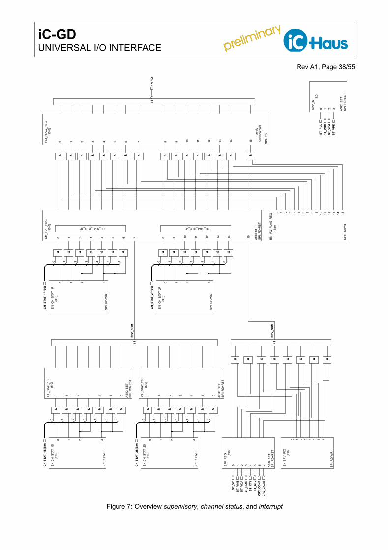
preliminary
preliminary iC-GDUNIVERSAL I/O INTERFACE
Rev A1, Page 38/55
4
1 6 7 8
AS
IC: S
ET
SP
I: R
D+R
ST
0
5
3
EN
_CH
_STA
T_2P
EN
_CH
_STA
T_2S
SP
I: R
D/W
R
0 1 2
9 10 11 12
0
4 5
6
5 13 15
14 15
3
5
7
7
9 10 11 12
2 3
AS
IC: S
ET
SP
I: R
D+R
ST
0 1 2 3 4 7
2
IRQ
_FLA
G_R
EG
pure
ly
147C
H_S
TAT_
2S
AS
IC: S
ET
0
com
bina
toria
l
(15:
0)
SP
I: R
D
(15:
0)
0 1 2 3
(7:0
)
0
(3:0
)(6
:0)
(3:0
)
(3:0
)
SP
I: R
D/W
R
(15:
0)
3 4 5 6
EN
_IR
Q_F
LAG
_RE
G
3
EN
_CH
_STA
T_1P
SP
I: R
D/W
R
0 1 2
6 13
13
CH_STAT_REG_1P
1 2
EN
_CH
_STA
T_1S
31 2
SP
I: R
D/W
R
SP
V_R
EG
AS
IC: S
ET
SP
I: R
D+R
ST
1
12
3 4 5
6
CH
_STA
T_R
EG
0SP
V_I
NT
AS
IC: S
ET
SP
I: R
D+R
ST
1 2 3
(3:0
)
2
0
EN
_SP
V_I
RQ
SP
I: R
D/W
R
1
15
SP
I: R
D/W
R
0
SP
I: R
D+R
ST
0 1
13 4
2 3
(3:0
)(6
:0)
4
2
84 5
6 14
6CH
_STA
T_1S
CH_STAT_REG_2P
(7:0
)
8 9 10 11& &
0 1
&&
&&
4
&
0
1
&
& &
&
&
&
&
&
2
1
1
&&
5
&
&
& & &5
&
&
&5
1
&&
&
0 1
&6
&6
&
&
&& &
&
2
&
&
&6
&
6&
&
3 4
&
& &
5
3
&
3
210
&
2 3 4
&
& &
&
&
SEC_SUM
ST_VB
ST_VNB
SPV_SUM
ST_VDA
ST_BIAS
ST_CT1
ST_CT2
CH_STAT_1P(6:0)
CH_STAT_1S(6:0)
CH_STAT_2S(6:0)
CH_STAT_2P(6:0)
CRC_CONF
CRC_CALIB
ST_PLL
ST_VBG
ST_VPA
ST_VPD
NIRQ
& &
&&
& &
& &
& & &
1
& &
1
&
&
& &
&& &
1
&
&
& && &
& &
&
& & &
&& &
&& &
& &
&
&
&
&
& &&
& &
&
&
&
Figure 7: Overview supervisory, channel status, and interrupt
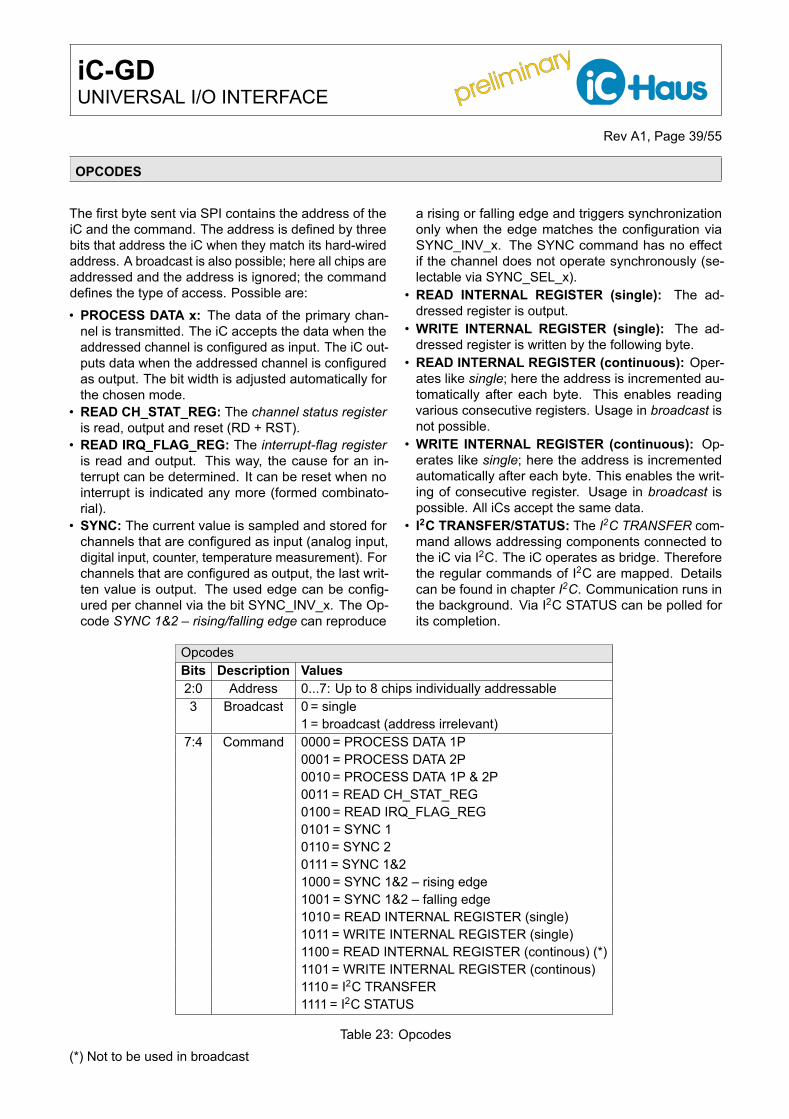
preliminary
preliminary iC-GDUNIVERSAL I/O INTERFACE
Rev A1, Page 39/55
OPCODES
The first byte sent via SPI contains the address of theiC and the command. The address is defined by threebits that address the iC when they match its hard-wiredaddress. A broadcast is also possible; here all chips areaddressed and the address is ignored; the commanddefines the type of access. Possible are:• PROCESS DATA x: The data of the primary chan-
nel is transmitted. The iC accepts the data when theaddressed channel is configured as input. The iC out-puts data when the addressed channel is configuredas output. The bit width is adjusted automatically forthe chosen mode.
• READ CH_STAT_REG: The channel status registeris read, output and reset (RD + RST).
• READ IRQ_FLAG_REG: The interrupt-flag registeris read and output. This way, the cause for an in-terrupt can be determined. It can be reset when nointerrupt is indicated any more (formed combinato-rial).
• SYNC: The current value is sampled and stored forchannels that are configured as input (analog input,digital input, counter, temperature measurement). Forchannels that are configured as output, the last writ-ten value is output. The used edge can be config-ured per channel via the bit SYNC_INV_x. The Op-code SYNC 1&2 – rising/falling edge can reproduce
a rising or falling edge and triggers synchronizationonly when the edge matches the configuration viaSYNC_INV_x. The SYNC command has no effectif the channel does not operate synchronously (se-lectable via SYNC_SEL_x).
• READ INTERNAL REGISTER (single): The ad-dressed register is output.
• WRITE INTERNAL REGISTER (single): The ad-dressed register is written by the following byte.
• READ INTERNAL REGISTER (continuous): Oper-ates like single; here the address is incremented au-tomatically after each byte. This enables readingvarious consecutive registers. Usage in broadcast isnot possible.
• WRITE INTERNAL REGISTER (continuous): Op-erates like single; here the address is incrementedautomatically after each byte. This enables the writ-ing of consecutive register. Usage in broadcast ispossible. All iCs accept the same data.
• I2C TRANSFER/STATUS: The I2C TRANSFER com-mand allows addressing components connected tothe iC via I2C. The iC operates as bridge. Thereforethe regular commands of I2C are mapped. Detailscan be found in chapter I2C. Communication runs inthe background. Via I2C STATUS can be polled forits completion.
OpcodesBits Description Values2:0 Address 0...7: Up to 8 chips individually addressable3 Broadcast 0 = single
1 = broadcast (address irrelevant)7:4 Command 0000 = PROCESS DATA 1P
0001 = PROCESS DATA 2P0010 = PROCESS DATA 1P & 2P0011 = READ CH_STAT_REG0100 = READ IRQ_FLAG_REG0101 = SYNC 10110 = SYNC 20111 = SYNC 1&21000 = SYNC 1&2 – rising edge1001 = SYNC 1&2 – falling edge1010 = READ INTERNAL REGISTER (single)1011 = WRITE INTERNAL REGISTER (single)1100 = READ INTERNAL REGISTER (continous) (*)1101 = WRITE INTERNAL REGISTER (continous)1110 = I2C TRANSFER1111 = I2C STATUS
Table 23: Opcodes(*) Not to be used in broadcast
preliminary
preliminary iC-GDUNIVERSAL I/O INTERFACE
Rev A1, Page 40/55
OPCODE-BASED DATA
PROCESS_DATA_xThe register PROCESS_DATA_x is controlled via theopcode and therefore does not contain a register ad-dress itself.
The meaning and length of the opcode complies withthe selected mode of the IO_SEL_x register and otherinvolved registers if applicable. The register can trans-mit 32-bit, 16-bit, and 8-bit data and optionally can beswitched off entirely. It contains the data of the primarychannels.
PROCESS_DATA_x (DI) P R - /bit 6:0 0000000bit 7 Digital input after spike filter, optionally inverted
Table 24: Process data primary channel in DI mode
PROCESS_DATA_x (DO/PWM) P RW - 0x00bit 6:0 0000000bit 7 OUT Output, depending on DO_SEL, optionally inverted:
PUSH-PULL: Output bitLOW-SIDE: 0 = line low (driver active)HIGH-SIDE: 1 = line high (driver active)
bit 7 IN(*) Reading of the physical line: digital input after spikefilter, optionally inverted
Table 25: Process data primary channel in DO mode
(*) No overlapping since there are different byes whenwriting and reading back.
PROCESS_DATA_x (VI/CI) P R - /bit 15:0 Analog input value, see Tab. 5
Table 26: Process data primary channel in VI/CI mode
PROCESS_DATA_x (VO/CO) P W - 0x0000bit 1:0 Unusedbit 15:2 Analog output value, see Tab. 7
Table 27: Process data primary channel in VO/COmode
PROCESS_DATA_x (CNT) P R(*) - 0x00000000
bit 31:0 Counter value (1 LSB = 125 ns)
Table 28: Process data primary channel in CNT mode
(*) Setting of the counter possible via register communi-cation.
PROCESS_DATA_x (TM) P R - /bit 15:0 Temperature, see Tab. 10
Table 29: Process data primary channel in TM mode
CH_STAT_REGThe register CH_STAT_REG is controlled directly viathe opcode and therefore does not contain a registeraddress.
The states of both primary channels and other sta-tus bits are stored in this register. The states of thechannels depend on the selected mode (IO_SEL_xP)and can be activated via the EN_CH_STAT_xP register.When reading, the bits are reset automatically.
Note that bit 2, 3, 4, 5, and 6 can only be (de-)activatedtogether because they are controlled by the same bitof the EN_CH_STAT_xP register. They assume theirstatus independently though. In the following tables thisis marked by horizontal lines.
Figure 7 explains the connection between the regis-ters CH_STAT, SPV_REG, IRQ_FLAG_REG, and theirenable registers.
CH_STAT_REG P+ R+RST - 0x0000bit 6:0 CH_STAT_1P, see Table 31 to 37bit 7 CH_STAT_12S_SUM – Sum of CH_STAT_1S and
CH_STAT_2Sbit 14:8 CH_STAT_2P, see Table 31 to 37bit 15 SPV_REG_SUM – Sum of SPV_REG
Table 30: Channel status register
CH_STAT_x (DI) P R+RST -0000000
bit 0 Mapping of digital input to spike filter and optionalinvertion (*)
bit 6 1 = Overcurrent UNx
Table 31: CH_STAT_x in DI mode
(*) When bit ENDOSC_x is activated, the output of thecomparator that is also available for SPI is mappedinstead.
preliminary
preliminary iC-GDUNIVERSAL I/O INTERFACE
Rev A1, Page 41/55
CH_STAT_x (DO / CNT(PWM)) P R+RST -0000000
bit 0 1 = Cable break (*)bit 1 1 = Channel overtemperature (***)bit 2 1 = Overcurrent IAx (**)bit 6 1 = Overcurrent UNx
Table 32: CH_STAT_x in DO/PWM mode
(*) Cable break detection is based on the pull-up/pull-down currents according to Item No. B04/B12.A cable break will only be detected when the driver isinactive and the connected load cannot pull away thecurrent, i.e. in the following operating conditions:
1) Low-side driver configured and switched off (i.e. out-put at ’1’).
2) High-side driver configured and switched off (i.e. out-put at ’0’).
The identification has a dead time of td(),ol, to alsoenable high-resistance loads to discharge the line.
(**) The status bit for overcurrent is activated when anactive driver cannot saturate anymore. This conditioncan be long-lasting, provided that the overtemperaturemonitoring remains inactive.
(***) The channel overtemperature, as defined inovertemperature behavior, switches off the digital driver.When the restart temperature is underrun, the driver isactivated automatically. Therefore the driver oscillateswith a thermal time-constant.
CH_STAT_x (VI/CI/TM(TE)) P R+RST -0000000
bit 0 1 = lower range underrunbit 1 1 = upper range overrunbit 2 1 = lower limit underrunbit 3 1 = upper limit overrunbit 4 1 = cable break UPx/current underrun (CI at
4...20 mA only)bit 5 1 = cable break UIxbit 6 1 = overcurrent UNx
Table 33: CH_STAT_x in mode VI/CI/TE
(*) The current underrun is only active during currentmeasurement operation with a configured 4 to 20 mArange and monitors the digital value for falling below0xFD00 = 3.602 mA.
CH_STAT_x (TM(PT)) P R+RST -0000000
bit 0 1 = lower range underrunbit 1 1 = upper range overrunbit 2 1 = lower limit underrunbit 3 1 = upper limit overrunbit 4 1 = cable break UPx (4-wire only)/cable break IA
(2/3/4-wire)bit 5 1 = cable break UIx (3/4-wire only)bit 6 1 = overcurrent UNx
Table 34: CH_STAT_x in mode TM(PT)
CH_STAT_x (VO) P R+RST -0000000
bit 0 1 = overcurrent UPx (pin higher than nominal)bit 1 1 = overcurrent UPx (pin lower than nominal)bit 6 1 = overcurrent UNx
Table 35: CH_STAT_x in mode VO
CH_STAT_x (CO) P R+RST -0000000
bit 0 1 = cable break/R_load(*) IAxbit 6 1 = overcurrent UNx
Table 36: CH_STAT_x in mode CO
(*) This bit is set if the cable at the relevant pin is bro-ken or the combination of load resistance and currentprevents the driver from saturatiing.
CH_STAT_x (CNT except PWM) P R+RST -0000000
bit 0 Mapping of digital input to spike filter and optionalinversion (*)
bit 1 1 = counter underrunbit 2 1 = counter overrunbit 4 1 = counter reached reference valuebit 5 1 = counter reached reference value #2 (CH_1 only,
see bit CNT_E2R)bit 6 1 = overcurrent UNx
Table 37: CH_STAT_x in mode CNT
(*) When bit ENDOSC_x is activated, the output ofthe comparator that is also available for the counter ismapped instead.
IRQ_FLAG_REGThe register IRQ_FLAG_REG is controlled directly viathe opcode and therefore does not contain a registeraddress.
The bits of the CH_STAT_REG register that were acti-vated via EN_IRQ_FLAG_REG are mapped to this reg-ister. IRQ_FLAG_REG is no register as such. It is gen-
preliminary
preliminary iC-GDUNIVERSAL I/O INTERFACE
Rev A1, Page 42/55
erated combinatorial and therefore can neither be writ-ten nor reset. To clear these bits, either CH_STAT_REGmust be read whereby set bits are reset or the detectionmust be deactivated in EN_IRQ_FLAG_REG. Figure 7
shows the connection between the registers CH_STAT,SPV and IRQ_FLAGS.
IRQ_FLAG_REG / R - NAbit 6:0 Active interrupts of CH_STAT_REG_1Pbit 7 Sum of active interrupts of
CH_STAT_REG_1S and CH_STAT_REG_2Sbit 14:8 Active interrupts of CH_STAT_REG_2Pbit 15 Sum of activen interrupts of SPV_REG
Table 38: IRQ-Flag-Register
REGISTER MAPAddr Bit 7 Bit 6 Bit 5 Bit 4 Bit 3 Bit 2 Bit 1 Bit 0
Configuration channel 10x00 ENVIF_1 IO_SEL_1S(2:0) DO_12 IO_SEL_1P(2:0)0x01 SYNC_INV_1 SYNC_SEL_1(1:0) DIO_INV_1 DO_SEL_1(1:0) DI_SEL_1(1:0)0x02 ENDOSC_1 CNT_E2R_1 VO_EC_1 CO_SEL_1(1:0) VICI_SEL_1(2:0)0x03(A) CNT_DUAL CNT_SEL_1(2:0) CNT_CBE_1 CNT_DNU_1 CNT_RAR_1 CNT_DCB_10x03(B) CNT_DUAL CNT_SEL_1(2:0) (unused) PWM_LAP_1 PWM_AZP_1 PWM_HS_10x03(C) TM_SEL_1(4:0)0x04 AI_LOWER_1(15:8)0x05 AI_LOWER_1(7:0)0x06 AI_UPPER_1(15:8)0x07 AI_UPPER_1(7:0)0x08 EN_CH_STAT_1S(3:0) EN_CH_STAT_1P(3:0)0x09 SPIKE_FIL_1(3:0) DIG_FIL_1(3:0)Configuration channel 20x10 ENVIF_2 IO_SEL_2S(2:0) DO_ADR0_2 IO_SEL_2P(2:0)0x11 SYNC_INV_2 SYNC_SEL_2(1:0) DIO_INV_2 DO_SEL_2(1:0) DI_SEL_2(1:0)0x12 ENDOSC_2 (unused) VO_EC_2 CO_SEL_2(1:0) VICI_SEL_2(2:0)0x13(A) (unused) CNT_SEL_2(2:0) CNT_CBE_2 CNT_DNU_2 CNT_RAR_2 CNT_DCB_20x13(B) (unused) CNT_SEL_2(2:0) (unused) (unused) PWM_AZP_2 PWM_HS_20x13(C) TM_SEL_2(4:0)0x14 AI_LOWER_2(15:8)0x15 AI_LOWER_2(7:0)0x16 AI_UPPER_2(15:8)0x17 AI_UPPER_2(7:0)0x18 EN_CH_STAT_2S(3:0) EN_CH_STAT_2P(3:0)0x19 SPIKE_FIL_2(3:0) DIG_FIL_2(3:0)Digital filter setting0x1B FIL_ITP_1 FIL_HB_1 FIL_ITP_2 FIL_HB_2
SPV_INT0x1F ST_VPD ST_VPA ST_VBG ST_PLL
preliminary
preliminary iC-GDUNIVERSAL I/O INTERFACE
Rev A1, Page 43/55
REGISTER MAPAddr Bit 7 Bit 6 Bit 5 Bit 4 Bit 3 Bit 2 Bit 1 Bit 0
Counter0x20 SET_CNT_1(31:24)0x21 SET_CNT_1(23:16)0x22 SET_CNT_1(15:8)0x23 SET_CNT_1(7:0)0x24 SET_CNT_2(31:24)0x25 SET_CNT_2(23:16)0x26 SET_CNT_2(15:8)0x27 SET_CNT_2(7:0)0x28 REF_CNT_1(31:24)0x29 REF_CNT_1(23:16)0x2A REF_CNT_1(15:8)0x2B REF_CNT_1(7:0)0x2C REF_CNT_2(31:24)0x2D REF_CNT_2(23:16)0x2E REF_CNT_2(15:8)0x2F REF_CNT_2(7:0)General configuration0x30 SEL_ETK VDA_VB EN_SS DIS_CAL DIS_SPI2 DIS_SPI1 EN_SPI_WD EN_UCM
EN_SPV_IRQ0x31 EN_CALIB EN_CONF EN_CT2 EN_CT1 EN_BIAS EN_VDA EN_VNB EN_VB
Interrupt enable0x32 EN_IRQ_FLAG_REG(15:8)0x33 EN_IRQ_FLAG_REG(7:0)Secondary channel data0x34 DATA_1S(15:8)0x35 DATA_1S(7:0)0x36 DATA_2S(15:8)0x37 DATA_2S(7:0)Watchdog0x38 WATCHDOG(7:0)SPI_LOCK, software reset0x39 SPI_LOCK_RESET(7:0)Cold-junction temperature0x3A TEMP_KSK(15:8)0x3B TEMP_KSK(7:0)Chip temperature0x3C CHIP_TEMP(7:0)Diagnostics measurements0x3D EN_DIAG DIAG_SEL_CH(3:0)0x3E DIAG(13:6)0x3F DIAG(5:0)Write EEPROM configuration0x40 WR_EEPROM_CONF(7:0)
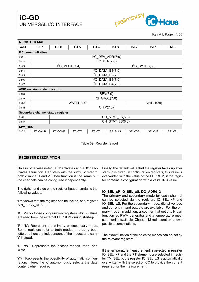
preliminary
preliminary iC-GDUNIVERSAL I/O INTERFACE
Rev A1, Page 44/55
REGISTER MAPAddr Bit 7 Bit 6 Bit 5 Bit 4 Bit 3 Bit 2 Bit 1 Bit 0
I2C communikation0x41 I2C_DEV_ADR(7:0)0x42 I2C_PTR(7:0)0x43 I2C_MODE(7:4) I2C_BYTES(3:0)0x44 I2C_DATA_B1(7:0)0x45 I2C_DATA_B2(7:0)0x46 I2C_DATA_B3(7:0)0x47 I2C_DATA_B4(7:0)ASIC revision & identification0x48 REV(7:0)0x49 CHARGE(7:0)0x4A WAFER(4:0) CHIP(10:8)0x4B CHIP(7:0)Secondary channel status register0x4E CH_STAT_1S(6:0)0x4F CH_STAT_2S(6:0)SPV_REG0x52 ST_CALIB ST_CONF ST_CT2 ST_CT1 ST_BIAS ST_VDA ST_VNB ST_VB
Table 39: Register layout
REGISTER DESCRIPTION
Unless otherwise noted, a ’1’ activates and a ’0’ deac-tivates a function. Registers with the suffix _x refer toboth channel 1 and 2. Their function is the same butthe channels can be configured independently.
The right hand side of the register header contains thefollowing values:
’L’: Shows that the register can be locked, see registerSPI_LOCK_RESET.
’K’: Marks those configuration registers which valuesare read from the external EEPROM during start-up.
’P’, ’S’: Represent the primary or secondary mode.Some registers refer to both modes and carry bothletters, others are independent of the modes and carry’/’ instead.
’R’, ’W’: Represents the access modes ’read’ and’write’.
’(*)’: Represents the possibility of automatic configu-ration. Here, the iC autonomously selects the datacontent when required.
Finally, the default value that the register takes up afterstart-up is given. In configuration registers, this value isoverwritten with the value of the EEPROM, if the regis-ter contains a configuration with a valid CRC value.
IO_SEL_xP, IO_SEL_xS, DO_ADR0_2The primary and secondary mode for each channelcan be selected via the registers IO_SEL_xP andIO_SEL_xS. For the secondary mode, digital voltageand current in- and outputs are available. For the pri-mary mode, in addition, a counter that optionally canfunction as PWM generator and a temperature mea-surement is available. Chapter ’Mixed operation’ showspossible combinations.
The exact function of the selected modes can be set bythe relevant registers.
If the temperature measurement is selected in registerIO_SEL_xP and the PT elements are selected in regis-ter TM_SEL_x, the register IO_SEL_xS is automaticallyoverwritten with the selection CO to provide the currentrequired for the measurement.
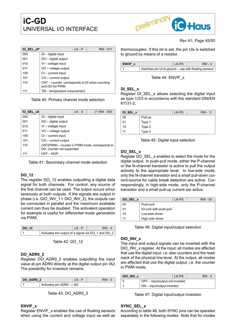
preliminary
preliminary iC-GDUNIVERSAL I/O INTERFACE
Rev A1, Page 45/55
IO_SEL_xP LK - P RW - 011000 DI – digital input001 DO – digital output010 VI – voltage input011 VO – voltage output100 CI – current input101 CO – current output110 CNT – counter, corresponds to DI when counting
and DO for PWM111 TM – temperature mesurement
Table 40: Primary channel mode selection
IO_SEL_xS LK - S (*) RW - 000000 DI – digital input001 DO – digital output010 VI – voltage input011 VO – voltage output100 CI – current input101 CO – current output110 CNT(PWM) – counter in PWM mode, corresponds to
DO; counter not supported111 OFF – NOP
Table 41: Secondary channel mode selection
DO_12The register DO_12 enables outputting a digital datasignal for both channels. For control, any source ofthe first channel can be used. The output occurs simul-taneously at both outputs. If the signals are output inphase (i.e. DIO_INV_1 = DIO_INV_2), the outputs canbe connected in parallel and the maximum availablecurrent can thus be doubled. The antivalent operationfor example is useful for differential mode generationvia PWM.
DO_12 LK - P RW - 01 Activates the output of a signal via DO_1 and DO_2
Table 42: DO_12
DO_ADR0_2Register DO_ADR0_2 enables outputting the inputvalue at pin ADR0 directly at the digital output pin IA2.The possibility for inversion remains.
DO_ADR0_2 LK - P RW - 01 Activates pin ADR0 → IA2
Table 43: DO_ADR0_2
ENVIF_xRegister ENVIF_x enables the use of floating sensorswhen using the current and voltage input as well as
thermocouples. If this bit is set, the pin UIx is switchedto ground by means of a resistor.
ENVIF_x LK-PS RW - 01 Switches pin UI to ground – use with floating sensors
Table 44: ENVIF_x
DI_SEL_xRegister DI_SEL_x allows selecting the digital inputas type 1/2/3 in accordance with the standard DIN/EN61131-2.
DI_SEL_x LK-PS RW - 1100 Pull-up01 Type 110 Type 211 Type 3
Table 45: Digital input selection
DO_SEL_xRegister DO_SEL_x enables to select the mode for thedigital output. In push-pull mode, either the P-channelor the N-channel transistor is active to pull the outputactively to the appropriate level. In low-side mode,only the N-channel transistor and a small pull-down cur-rent-source for cable break detection are active. Cor-respondingly, in high-side mode, only the P-channeltransistor and a small pull-up current are active.
DO_SEL_x LK-PS RW - 0000 Push-pull01 IO-Link with push-pull10 Low-side driver11 High-side driver
Table 46: Digital input/output selection
DIO_INV_xThe input and output signals can be inverted with theDIO_INV_x register. At the input, all modes are affectedthat use the digital input, i.e. also counters and the read--back of the physical line level. At the output, all modesare affected that use the digital output, i.e. the counterin PWM mode.
DIO_INV_x LK-PS RW - 00 OFF – input/output not inverted1 ON – input/output inverted
Table 47: Digital input/output inversion
SYNC_SEL_xAccording to table 48, both SYNC pins can be operatedseparately in the following modes. Note that for modes
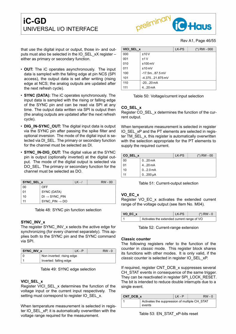
preliminary
preliminary iC-GDUNIVERSAL I/O INTERFACE
Rev A1, Page 46/55
that use the digital input or output, those in- and out-puts must also be selected in the IO_SEL_xX register –either as primary or secondary function.
• OUT: The iC operates asynchronously. The inputdata is sampled with the falling edge at pin NCS (SPIaccess), the output data is set after writing (risingedge at NCS; the analog outputs are updated afterthe next refresh cycle).
• SYNC (DATA): The iC operates synchronously. Theinput data is sampled with the rising or falling edgeof the SYNC pin and can be read via SPI at anytime. The output data written via SPI is output then(the analog outputs are updated after the next refreshcycle).
• DIG_IN-SYNC_OUT: The digital input data is outputvia the SYNC pin after passing the spike filter andoptional inversion. The mode of the digital input is se-lected via DI_SEL. The primary or secondary functionfor the channel must be selected as DI.
• SYNC_IN-DIG_OUT: The digital value at the SYNCpin is output (optionally inverted) at the digital out-put. The mode of the digital output is selected viaDO_SEL. The primary or secondary function for thechannel must be selected as DO.
SYNC_SEL_x LK - / RW - 0000 OFF01 SYNC (DATA)10 DI → SYNC_PIN11 SYNC_PIN → DO
Table 48: SYNC pin function selection
SYNC_INV_xThe register SYNC_INV_x selects the active edge forsynchronizing (for every channel separately). This ap-plies both to the SYNC pin and the SYNC commandvia SPI.
SYNC_INV_x LK - P RW - 00 Non inverted: rising edge1 Inverted: falling edge
Table 49: SYNC edge selection
VICI_SEL_xRegister VICI_SEL_x determines the function of thevoltage input or the current input respectively. Thesetting must correspond to register IO_SEL_x.
When temperature measurement is selected in regis-ter IO_SEL_xP, it is automatically overwritten with thevoltage range required for the measurement.
VICI_SEL_x LK-PS (*) RW - 000000 ±10 V001 ±1 V010 ±100 mV011 ±10 mV100 -17.5m...87.5 mV101 -4.375...21.875 mV110 -20...20 mA111 4...20 mA
Table 50: Voltage/current input selection
CO_SEL_xRegister CO_SEL_x determines the function of the cur-rent output.
When temperature measurement is selected in registerIO_SEL_xP and the PT elements are selected in regis-ter TM_SEL_x, this register is automatically overwrittenwith the selection appropriate for the PT elements tosupply the required current.
CO_SEL_x LK-PS (*) RW - 0000 0...20 mA01 4...20 mA10 0...2.0 mA11 0...200µA
Table 51: Current-output selection
VO_EC_xRegister VO_EC_x activates the extended currentrange of the voltage output (see Item No. M04).
VO_EC_x LK-PS (*) RW - 01 Activates the extended current range of VO
Table 52: Current-range extension
Classic counterThe following registers refer to the function of thecounter in classic mode. This register block sharesits functions with other modes. It is only valid, if theclassic counter is selected in register IO_SEL_xP.
If required, register CNT_DCB_x suppresses severalCH_STAT events in consequence of the same trigger.They can be reactivated in register SPI_LOCK_RESET.The bit is intended to reduce double interrupts due to asingle event.
CNT_DCB_x LK - P RW - 01 Activates the suppression of multiple CH_STAT
events
Table 53: EN_STAT_xP-bits reset
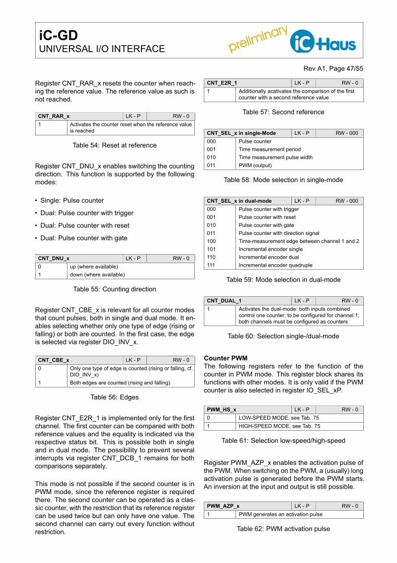
preliminary
preliminary iC-GDUNIVERSAL I/O INTERFACE
Rev A1, Page 47/55
Register CNT_RAR_x resets the counter when reach-ing the reference value. The reference value as such isnot reached.
CNT_RAR_x LK - P RW - 01 Activates the counter reset when the reference value
is reached
Table 54: Reset at reference
Register CNT_DNU_x enables switching the countingdirection. This function is supported by the followingmodes:
• Single: Pulse counter
• Dual: Pulse counter with trigger
• Dual: Pulse counter with reset
• Dual: Pulse counter with gate
CNT_DNU_x LK - P RW - 00 up (where available)1 down (where available)
Table 55: Counting direction
Register CNT_CBE_x is relevant for all counter modesthat count pulses, both in single and dual mode. It en-ables selecting whether only one type of edge (rising orfalling) or both are counted. In the first case, the edgeis selected via register DIO_INV_x.
CNT_CBE_x LK - P RW - 00 Only one type of edge is counted (rising or falling, cf.
DIO_INV_x)1 Both edges are counted (rising and falling)
Table 56: Edges
Register CNT_E2R_1 is implemented only for the firstchannel. The first counter can be compared with bothreference values and the equality is indicated via therespective status bit. This is possible both in singleand in dual mode. The possibility to prevent severalinterrupts via register CNT_DCB_1 remains for bothcomparisons separately.
This mode is not possible if the second counter is inPWM mode, since the reference register is requiredthere. The second counter can be operated as a clas-sic counter, with the restriction that its reference registercan be used twice but can only have one value. Thesecond channel can carry out every function withoutrestriction.
CNT_E2R_1 LK - P RW - 01 Additionally acativates the comparison of the first
counter with a second reference value
Table 57: Second reference
CNT_SEL_x in single-Mode LK - P RW - 000000 Pulse counter001 Time measurement period010 Time measurement pulse width011 PWM (output)
Table 58: Mode selection in single-mode
CNT_SEL_x in dual-mode LK - P RW - 000000 Pulse counter with trigger001 Pulse counter with reset010 Pulse counter with gate011 Pulse counter with direction signal100 Time-measurement edge between channel 1 and 2101 Incremental encoder single110 Incremental encoder dual111 Incremental encoder quadruple
Table 59: Mode selection in dual-mode
CNT_DUAL_1 LK - P RW - 01 Activates the dual-mode: both inputs combined
control one counter; to be configured for channel 1;both channels must be configured as counters
Table 60: Selection single-/dual-mode
Counter PWMThe following registers refer to the function of thecounter in PWM mode. This register block shares itsfunctions with other modes. It is only valid if the PWMcounter is also selected in register IO_SEL_xP.
PWM_HS_x LK - P RW - 00 LOW-SPEED MODE, see Tab. 751 HIGH-SPEED MODE, see Tab. 75
Table 61: Selection low-speed/high-speed
Register PWM_AZP_x enables the activation pulse ofthe PWM. When switching on the PWM, a (usually) longactivation pulse is generated before the PWM starts.An inversion at the input and output is still possible.
PWM_AZP_x LK - P RW - 01 PWM generates an activation pulse
Table 62: PWM activation pulse
preliminary
preliminary iC-GDUNIVERSAL I/O INTERFACE
Rev A1, Page 48/55
The bit PWM_LAP_1 (only present in the first channel)is intended for operation of the PWM in antivalent mode.If it is active and a channel is inverted in active mode(DO = ’1’), both outputs operate in antivalent mode. Ininactive mode, (DO = ’0’) both outputs are set to thesame state depending on DIO_INV_1 and _2 either ’0’or ’1’. The use of this bit requires the bit DO_12.
PWM_LAP_1 LK - P RW - 01 PWM_2 anitvalent or in phase with PWM_1 when off
Table 63: PWM antivalent gating
TM_SEL_xThe following registers refer to the function of tempera-ture measurement. This register block shares its func-tions with other modes. It is only valid if the temperaturemeasurement is also selected in the IO_SEL_xP regis-ter.
The thermocouples do not require any further settingsexcept the selection of the temperature measurement inregister IO_SEL_x, i.e. the voltage measurement range
is selected automatically by the iC. The same applies tothe PT-temperature sensors, whereas, additionally, therequired current must be set as secondary function, i.e.both registers CO_SEL_x and DATA_xS. The currentmust be selected in such a way that the nominal valuei.e. at 0 °C results in a voltage of exactly 170 mV. Table65 helps selecting appropriate output currents.
TM_SEL_x LK - P RW - 0000000000 Thermo-couple J00001 Thermo-couple K00010 Thermo-couple T00011 Thermo-couple N00100 Thermo-couple E00101 Thermo-couple R00110 Thermo-couple S00111 Thermo-couple B11000 PT sensor, 2-wire11001 PT sensor, 3-wire11010 PT sensor, 4-wire
Table 64: Temperature measurement selection
PT-Element CO_SEL_x DATA_xSPT100 0...2 mA (10) 1.7 mA (0xCF3C)PT200 0...2 mA (10) 0.85 mA (0x67A0)PT300 0...2 mA (10) 0.5667 mA (0x4514)PT500 0...2 mA (10) 0.34 mA (0x2974)PT1000 0...200µA (11) 170µA (0xCF3C)PT2000 0...200µA (11) 85µA (0x67A0)PT3000 0...200µA (11) 56.67µA (0x4514)PT5000 0...200µA (11) 34µA (0x2974)PT9000 0...200µA (11) 18.89µA (0x1708)
Table 65: PT current selection examples
EN_CH_STAT_xXRegister EN_CH_STAT_xX activates the bits of regis-ter CH_STAT_xX. Note that bits 2, 3, 4, 5, and 6 canonly be activated en masse. This is relevant for thelimit detection. This limit can easily be restricted to justexceeding or falling below by setting the appropriatelimit value to the maximum or minimum of the range.Figure 7 shows the connection between the registersCH_STAT, SPV and IRQ_FLAG_REG.
CH_STAT_xX LK-PS RW - 0x0bit0 activates relevant CH_STAT_xX, bit 0bit1 activates relevant CH_STAT_xX, bit 1bit2 activates relevant CH_STAT_xX, bits 2, 3bit3 activates relevant CH_STAT_xX, bits 4, 5, 6
Table 66: CH status
DIG_FIL_xVia register DIG_FIL_x, the cut-off frequency of the dig-ital filter can be set to filter the analog signals after theAD converter. The cut-off frequencies also depend onregister FIL_HB_x.
preliminary
preliminary iC-GDUNIVERSAL I/O INTERFACE
Rev A1, Page 49/55
DIG_FIL_x LK-PS RW - 0x0valid for FIL_HB_x = ’0’
0x0 2 kHz0x1 1 kHz0x2 500 Hz0x3 250 Hz0x4 125 Hz0x5 62.5 Hz0x6 31.2 Hz0x7 15.6 Hz0x8 7.8 Hz0x9 3.9 Hz0xA 1.9 Hz0xB 0.97 Hz0xC 0.50 Hz
valid for FIL_HB_x = ’1’0x0 3.50 kHz (only with voltage measurement)0x1 1.75 kHz (only with voltage measurement)0x2 875 Hz0x3 440 Hz0x4 220 Hz0x5 110 Hz0x6 55 Hz0x7 27.5 Hz0x8 14 Hz0x9 7 Hz0xA 3.5 Hz0xB 1.75 Hz0xC 0.875 Hz
Table 67: Digitale filter cut-off frequencies (rounded)
FIL_HB_xVia register FIL_HB_x, the digital input filter for the ana-log signals can be switched into a faster mode withreduced latency but flatter amplitude response. Thisinvolves an internal deactivation of the half-band filters.See register ’DIG_FIL_x’.
FIL_HB LK-PS RW - 00 Steeper amplitude response with higher latency1 Flatter amplitude response with lower latency
Table 68: FIL_HB_x
FIL_ITP_xVia register FIL_ITP_x, the digital input filter for theanalog signals can be switched into a faster mode withreduced latency but much lower sample rate. This in-volves a deactivation of the interpolation which resultsin about halving the latency.
FIL_ITP LK-PS RW - 00 Active interpolation with higher latency1 Deactive interpolation with lower latency
Table 69: FIL_ITP_x
SPIKE_FIL_xThe digital spike filter can be set for every channel sep-arately. It serves to filter the digital input for spuriouspulses up to a configurable length.
The digital spike filter can be set via the 4-bit-wide regis-ter SPIKE_FIL_x in the range of 0 up to approx. 262 ms.To deactivate the filter, the time can be set to 0. Inter-nally, the filter operates with an 8-bit counter. If the inputis 0, the counter is counted down, if it is 1, it is countedup. If the counter reaches 0, the output is set to 0. Ifthe counter achieves its maximum value dependent onthe filter width, it is set to 1.
Table 70 summarizes the settings of SPIKE_FIL_x, theresulting filter time and in brackets the internal samplerate and filter width. The given times have an accuracyof ±1 clock. This is equal to an accuracy e.g. at 8 MHzsampling of ±125 ns.
SPIKE_FIL_x LK-PS RW - 0x70x0 0µs . . . . . . . . . . . . . . . . . . . . . . . . . (8 MHz, spike-filter off)0x1 16µs . . . . . . . . . . . . . . . . . . . . . . . . (8 MHz, 7-bit counter)0x2 32µs . . . . . . . . . . . . . . . . . . . . . . . . (8 MHz, 8-bit counter)0x3 64µs . . . . . . . . . . . . . . . . . . . . . . . . (4 MHz, 8-bit counter)0x4 128µs . . . . . . . . . . . . . . . . . . . . . . . (2 MHz, 8-bit counter)0x5 256µs . . . . . . . . . . . . . . . . . . . . . . . (1 MHz, 8-bit counter)0x6 512µs . . . . . . . . . . . . . . . . . . . . . (500 kHz, 8-bit counter)0x7 1.024 ms . . . . . . . . . . . . . . . . . . . (250 kHz, 8-bit counter)0x8 2.048 ms . . . . . . . . . . . . . . . . . . . (125 kHz, 8-bit counter)0x9 4.096 ms . . . . . . . . . . . . . . . . . . (62.5 kHz, 8-bit counter)0xA 8.192 ms . . . . . . . . . . . . . . . . . (31.25 kHz, 8-bit counter)0xB 16.38 ms . . . . . . . . . . . . . . . . . (15.63 kHz, 8-bit counter)0xC 32.77 ms . . . . . . . . . . . . . . . . . (7.813 kHz, 8-bit counter)0xD 65.54 ms . . . . . . . . . . . . . . . . . (3.906 kHz, 8-bit counter)0xE 131.1 ms . . . . . . . . . . . . . . . . . (1.953 kHz, 8-bit counter)0xF 262.1 ms . . . . . . . . . . . . . . . . . (0.977 kHz, 8-bit counter)
Table 70: Spike-filtertime setting
AI_LOWER_x, AI_UPPER_xRegisters AI_LOWER_x and AI_UPPER_x describethe valid range in which the analog input should stay. Ifthe detection in the EN_CH_STAT_xX register is acti-vated, a status bit indicates when this range is left. Thestatus bit remains set until the status register is read toensure that temporarily leaving the range will also bedetected.
preliminary
preliminary iC-GDUNIVERSAL I/O INTERFACE
Rev A1, Page 50/55
AI_LOWER_x LK-PS RW - 0x8000bits 15:0 Lower limit (last valid value)
Table 71: Lower limit
AI_UPPER_x LK-PS RW - 0x7FFFbits 15:0 Upper limit (last valid value)
Table 72: Upper limit
SPV_INTRegister SPV_INT monitors the internal status. In caseof an error, the relevant bit is set to ’1’ and remainsset until the register is read via SPI. The register isshown in figure 7. It is not linked to the others registersthough.
SPV_INT / R - 0x00ST_PLL Status PLLST_VBG Status band-gap voltage VBGST_VPA Status internal supply voltage VDPST_VPD Status internal supply voltage VPD
Table 73: Internal monitor bits status
SET_CNT_xRegister SET_CNT_x enables setting the particularcounter to a specific value. Via the register communica-tion, the register can be set both in single or continuousmode. When writing the last register byte, the written16/32-bit-wide word is taken as a whole. In regularcounter modes, only setting the register as a whole isuseful. In PWM mode or with activation pulse mode,either the entire register or only the lower half (bits 15:0)can be set. Except for this, a partial writing of the regis-ter is not possible. The meaning of the register dependson the selected mode (see chapter ’Counter’).
SET_CNT_x P W - 0x00000000bits 31:0 Counter value
Table 74: Set counter
REF_CNT_xRegister REF_CNT_x enables setting the counter ref-erence value. Via the register communication, theregister can be set both in single and in continuousmode. When writing on the last register byte, the written16/32-bit-wide word is taken as a whole. It is possibleto set the register as a whole (bits 31:0) or to set onlythe lower half (bits 15:0). In PWM mode, it is usefulto set only the lower half (bits 15:0). Except for this, apartial writing of the register is not possible. The mean-ing of the register depends on the selected mode (seechapter ’Counter’).
REF_CNT_x P RW -0x00000000
Bits 31:0 Reference value
Table 75: Set counter reference
MonitoringThe bits of the monitoring register signal errors of indi-vidual supply voltages and overtemperature. In caseof an error, the relevant bit is set to ’1’ and remains setuntil the register is read out via the SPI. This enablesto detect voltage dips that occurred temporarily.
SPV_REG / R - 0x00ST_VB Supply voltage VBST_VNB Supply voltage VNBST_VDA Supply voltage VDAST_BIAS Bias (RREF)ST_CT1 Chip temperature 1 (cf. Toff1)ST_CT2 Chip temperature 2 (cf. Toff2)ST_CONF Configuration (CRC error)ST_CALIB Configuration (CRC error)
Table 76: Supervisory bits
EN_SPV_IRQ LK - / RW - 0x00EN_VB VB monitor activationEN_VNB VNB monitor activationEN_VDA VDA monitor activationEN_BIAS Bias monitor activationEN_CT1 CT1 monitor activationEN_CT2 CT2 monitor activationEN_CONF Configuration monitor activationEN_CALIB Configuration monitor activation
Table 77: Supervisory bits activation
EN_IRQ_FLAG_REGThe bits in register EN_IRQ_FLAG_REG activate therelevant bits in register IRQ_FLAG individually.
EN_IRQ_FLAG_REG LK - / RW - 0x0000bit 15:0 Activates individual bits of register
IRQ_FLAG_REG(15:0)
Table 78: IRQ flag activation
DATA_xSRegisters DATA_xS contain data of the secondary chan-nel. If the secondary channel operates as input, thecurrent values of the secondary channel can be read. Ifthe secondary channel operates as output, output datacan be written to the register. The communication pro-ceeds via the regular register communication in singleor continuous mode.
preliminary
preliminary iC-GDUNIVERSAL I/O INTERFACE
Rev A1, Page 51/55
Applying for modes using 16-bit wide values:
When the data is read, the lower half of the registerword is latched to ensure that a valid word is read out.When the data is written, the word is assumed as awhole only after transmission of the lower half.
Applying for modes using 8 bit wide values:
The values must be written or read left-aligned, i.e. onlythe bits 15:8 are used.
Usually, data is formatted identically to the data of theprimary channels.
DATA_xS S (*) RW - 0x0000Secondary channel data (in/out)
Table 79: Secondary channel data
EN_UCMVia register EN_UCM, SPI communication can be se-lected between FPGA and µC mode. In FPGA mode,the bit is ’0’ for all iCs. In µC mode, the bit is ’0’ for alliCs except the last iC which must be ’1’.
EN_UCM LK - / RW - 00 FPGA modus: no additional delay1 µC mode: additional clocks
Table 80: µC mode
EN_SPI_WDRegister EN_SPI_WD activates the watchdog which isused for SPI communication. If the watchdog is activeand no valid SPI communication takes place during adetermined period, the watchdog resets the chip. De-tails can be found in chapter ’Startup, reset, watchdogs,and EEPROM’.
EN_SPI_WD LK - / RW - 00 SPI watchdog inactive1 SPI watchdog active
Table 81: SPI watchdog
DIS_SPI_xWhen required, register DIS_SPI_x deactivates the pro-cess data of the SPI communication for channel x. Thisbit affects only the opcodes "Process Data 1/2/1&2". Ifa channel is not used, it does not require time by settingthis bit during the SPI communication. An interestinguse is in broadcast operation with chains of iCs withpartially unused channels.
DIS_SPI_x LK - P RW - 00 Channel x active1 Channel x inactive
Table 82: Disable SPI CH_x
DIS_CALWhen required, register DIS_CAL deactivates the cali-bration of the chip. This register is checked only whenthe chip starts up, therefore its state must be stored inthe EEPROM.
DIS_CAL LK-PS RW - 00 Calibration active1 Calibration inactive
Table 83: Disable channel calibration
EN_SSWhen required, register EN_SS activates the spectrumspread of the internal oscillator.
EN_SS LK - / RW - 00 Spread spectrum inactive1 Spread spectrum active
Table 84: Enable spread spectrum
VDA_VBWhen the digital output is not used, register VDA_VBenables to omit the 24 V digital supply voltage. Instead,the analog voltage VB can be connected to the pin VDA.In this case this bit should be set to adapt the internalvoltage monitoring accordingly.
VDA_VB LK - / RW - 00 VDA = 24 V, digital output used1 VDA = VB, digital output not used
Table 85: VDA at VB
SEL_ETKRegister SEL_ETK selects the calibration values thatare used for the TK compensation and chip-temper-ature calibration (ATK, AITK, and AOCT). These caneither be taken from the internal chip, if they were spec-ified in the chip production process, or they can betaken from the external EEPROM where they can bespecified subsequently. Independent of their use, thevalues that are stored in the EEPROM are used for thecalculation of the CRC value.
preliminary
preliminary iC-GDUNIVERSAL I/O INTERFACE
Rev A1, Page 52/55
SEL_ETK LK - / RW - 00 Internal calibration values are used1 External calibration values are used
Table 86: SEL_ETK
SPI_LOCK_RESETRegister SPI_LOCK_RESET is not a classical register.It possesses multiple functions that can be activated bywriting keywords: When writing 0xCA, a software resetis triggered – the chip restarts. When writing 0xA5, theSPI access for all registers is enabled in accordancewith the register overview. Writing 0x00 (and furtherbytes) disables writing access of the SPI to the configu-ration registers marked with ’L’. After configuration, thishelps to prevent accidental writing on the configurationregisters in regular operation.
When writing 0xC5, the counter enables a one-shotCH_STAT event (prevention of multiple interrupts at oneevent). This only affects the counter if the bit CNT_DCBis set.
Writing with 0xAA activates a special calibration modewhere registers that are usually inaccessible are addi-tionally unlocked. In this process, the usually activeaddress translation is switched off so that some regis-ters change their addresses. This function should onlybe activated during calibration and only according tothe extent described in chapter ’Calibration’.
When reading, this register returns four bits of sta-tus information. These bits are reset by read access(RD+RST). The first status bit is set if an illegal readaccess occured. The second status bit is set if an ille-gal write access occured. This relates both to lockedregisters and the access of non-existing addresses.
Note that a prefetching proceeds in modeREAD_REG_CONTINOUS. As a result, illegal readaccesses that already occur internally may be indicatedwithout being deliberately controlled by the SPI. Thethird status bit indicates the condition of the lock.
(*) The initial state of this ’register’ depends on the va-lidity of the configuration data. If a valid configuration isstored in the EEPROM, the SPI is locked after startingup the chip. If the configuration is invalid, the SPI is notlocked.
SPI_LOCK_RESET / RW+RST - (*)bit 0 read Status illegal read, 1 = detectedbit 1 read Status illegal write, 1 = detectedbit 2 read Status lock, 1 = lockedbit 3 read Status calibration mode, 1 = activebit 7:4 read 00000xCA write Software reset0xA5 write Configuration register write enabled0xC5 write CNT_STAT_REARM: signle CH_STAT
counter event enabled (*)0xAA write Calibration mode enabled. Caution! Further
parts of the register map become invalid, seesection ’Calibration’.
0x00 write Configuration register write disabled
Table 87: SPI lock/reset
(*) Unlocking refers to the following 4 states: overflow,underflow, REF_1 reached, REF_2 reached.
TEMP_KSKRegister TEMP_KSK contains the cold junction tem-perature that is necessary for the thermocouple mea-surement. The register can be written both in singleand continuous mode. It accepts its value internallyonly when the writing process of the second half is com-pleted so that a consistent value is processed. It canonly be written to as a whole.
TEMP_KSK P RW - 0x0BA6(=25°C)
bits 15:0 Cold-position temperature,0x0000 = 0K, 1 LSB = 0.1 K
Table 88: Cold-position temperature
CHIP_TEMPCHIP_TEMP / R - /bits 7:0 Chip temperature, 0x00 = -64 °C, 1 LSB = 1 °C
Table 89: Chip temperature
EN_DIAGRegister EN_DIAG activates the diagnostic measure-ment. The channel for analysis is selected via registerDIAG_SEL_CH. The result is continuously updated inregister DIAG_CH with an update frequency in accor-dance with the analog output. The first valid measure-ment value must be waited for accordingly.
EN_DIAG / RW - 01 Diagnostic modus active
Table 90: Diagnostics channel selection
preliminary
preliminary iC-GDUNIVERSAL I/O INTERFACE
Rev A1, Page 53/55
DIAG_SEL_CHDIAG_SEL_CH / RW - 00000000 VB0001 VNB0010 VCC0011 VDA0100 VPA0101 VPD0110 VI0111 V0201000 V4201001 Channel 1: Digital output current1010 Channel 2: Digital output current
Table 91: Diagnostics selection
DIAG_CH / R - /see Tab. 12
Table 92: Diagnostics channel
WR_EEPROM_CONFRegister WR_EEPROM_CONF stores the current con-figuration. After writing 0x96 to this register, the chipautomatically writes the current configuration, i.e. allregisters marked with ’K’, to the EEPROM. Subse-quently, also the valid CRC checksum is written. Whenthe writing process is completed, the register is set;0 signifies error-free writing, 1 signifies an error. Thisregister can be polled for the end of the writing process.
WR_EEPROM_CONF L - / RW - 0x000x96 write Starts write0x96 read Write in progress0x00 read Last write succesfull0x01 read Last write failed
Table 93: Write configuration
I2CThe chip contains an I2C interface. An external EEP-ROM must be connected to it which contains the con-figuration and calibration data required for operation.Additionally, it enables accessing other chips in the formof a bridge between SPI and I2C. For example temper-ature sensors with I2C interface can be controlled andtheir temperature data can be written via SPI on theregisters of the cold junction compensation.
The currently valid configuration data can be trans-mitted automatically to the EEPROM via registerWR_EEPROM_CONF. The calibration data must bewritten to the EEPROM in bridge mode and the match-ing checksums must be transmitted.
In all cases, the chip operates as an I2C master at upto 100 kbit/s. The interface is not capable of multi-mas-ter operation. The 7-bit addressing mode is supported.Note that an EEPROM with a page size of at least 2bytes is required for operation. When writing severalbytes to EEPROM it must be additionally ensured thatthe page limit is not exceeded. More information canbe found in the relevant datasheet.
The following registers are of importance to use thebridge:
• I2C_DEV_ADR: This register contains the address ofthe chips to be addressed, e.g. 0xA0 for EEPROMs
• I2C_PTR: This register operates as pointer. It ad-dresses a particular register at the addressed chip.
• I2C_MODE: According to table 96, it can be selectedbetween the modes RD; RD[PTR], and WR[PTR].
• I2C_BYTES: This register indicates the number ofbytes that are to be read or written. Values between1 and 4 are valid.
• I2C_DATA_Bx: During the writing process, the bytesstored here are written; during read process the bytesthat are read are stored here.
Except for the data bytes, no I2C register is changedduring I2C communication. A valid setting can be main-tained for an infinite time. If the registers are set cor-rectly, the communication can be started via opcodeI2C-TRANSFER. Opcode I2C Status can be polled forits end. Note that after successful writing accesses,EEPROMs require time for the internal writing. Withinthis time-window it does not respond to requests. Whenwriting, a waiting period in accordance with the EEP-ROM specification is to be maintained.
I2C_DEV_ADR / RW - undefChip address
Table 94: I2C device address
I2C_PTR / RW - undefPointer to address the chip
Table 95: I2C pointer
I2C_MODE / RW - undef0x1 RD: Read from current address0x2 RD[PTR]: Write from [PTR]0x4 WR[PTR]: Read from [PTR]
Table 96: I2C mode
I2C_DATA_Bx / RW - undefData bytes for I2C communikation
Table 97: I2C data bytes
preliminary
preliminary iC-GDUNIVERSAL I/O INTERFACE
Rev A1, Page 54/55
Feedback opcode I2C status / R - undef0x00 Communication ended successful0x01 Communication running0x03 Communication failed
Table 98: Opcode I2C status
Revision and identificationRegister REV contains the hardware revision numberof the iC, beginning with 1. The registers LOT, WAFERand CHIP set up a unique identification number definedduring chip production.
REV / R - /bits 7:0 Hardware revision number
Table 99: Revision number
LOT / R - /bits 7:0 Lot number
Table 100: Lot number
WAFER / R - /bits 4:0 Wafer number
Table 101: Wafer number
CHIP / R - /bits 10:0 Chip number
Table 102: Chip number
WATCHDOGRegister WATCHDOG provides information on thecause of the last reset. If all bits are 0, the iC restartedbecause of a power-on reset. Otherwise, exactly onebit is set according to table 103. Details can be foundin chapter ’Startup, Reset, Watchdogs, and EEPROM’.
WATCHDOG / R - 0x0bit 0 NRES pinbit 1 SW resetbit 2 SPI watchdogbit 3 µP watchdog
Table 103: Watchdog
CH_STAT_xSRegister CH_STAT_xS contains the status bits of thesecondary channel. The meaning of the bits dependson the selected mode IO_SEL_xS. The meaning isidentical with the meaning of the primary channel.
CH_STAT_xS S R - 0000000bits 6:0 see Tab. 31 to 37
Table 104: Secondary channel status register
iC-Haus expressly reserves the right to change its products and/or specifications. An Infoletter gives details as to any amendments and additions made to therelevant current specifications on our internet website www.ichaus.com/infoletter and is automatically generated and shall be sent to registered users by email.Copying – even as an excerpt – is only permitted with iC-Haus’ approval in writing and precise reference to source.
The data specified is intended solely for the purpose of product description and shall represent the usual quality of the product. In case the specifications containobvious mistakes e.g. in writing or calculation, iC-Haus reserves the right to correct the specification and no liability arises insofar that the specification was froma third party view obviously not reliable. There shall be no claims based on defects as to quality in cases of insignificant deviations from the specifications or incase of only minor impairment of usability.No representations or warranties, either expressed or implied, of merchantability, fitness for a particular purpose or of any other nature are made hereunderwith respect to information/specification or the products to which information refers and no guarantee with respect to compliance to the intended use is given. Inparticular, this also applies to the stated possible applications or areas of applications of the product.
iC-Haus products are not designed for and must not be used in connection with any applications where the failure of such products would reasonably beexpected to result in significant personal injury or death (Safety-Critical Applications) without iC-Haus’ specific written consent. Safety-Critical Applicationsinclude, without limitation, life support devices and systems. iC-Haus products are not designed nor intended for use in military or aerospace applications orenvironments or in automotive applications unless specifically designated for such use by iC-Haus.iC-Haus conveys no patent, copyright, mask work right or other trade mark right to this product. iC-Haus assumes no liability for any patent and/or other trademark rights of a third party resulting from processing or handling of the product and/or any other use of the product.
Software and its documentation is provided by iC-Haus GmbH or contributors "AS IS" and is subject to the ZVEI General Conditions for the Supply of Productsand Services with iC-Haus amendments and the ZVEI Software clause with iC-Haus amendments (www.ichaus.com/EULA).
preliminary
preliminary iC-GDUNIVERSAL I/O INTERFACE
Rev A1, Page 55/55
ORDERING INFORMATION
Type Package Order Designation
iC-GD QFN38 5 mm x 7 mm iC-GD QFN38-5x7
Please send your purchase orders to our order handling team:
Fax: +49 (0) 61 35 - 92 92 - 692E-Mail: [email protected]
For technical support, information about prices and terms of delivery please contact:
iC-Haus GmbH Tel.: +49 (0) 61 35 - 92 92 - 0Am Kuemmerling 18 Fax: +49 (0) 61 35 - 92 92 - 192D-55294 Bodenheim Web: http://www.ichaus.comGERMANY E-Mail: [email protected]
Appointed local distributors: http://www.ichaus.com/sales_partners