Embed Size (px)
Citation preview
IEEE TRANSACTIONS ON ANTENNAS AND PROPAGATION, VOL. 58, NO. 4, APRIL 2010 1093
CMOS Phased Array Transceiver Technology for60 GHz Wireless Applications
Mohammad Fakharzadeh, Member, IEEE, Mohammad-Reza Nezhad-Ahmadi,Behzad Biglarbegian, Student Member, IEEE, Javad Ahmadi-Shokouh, Member, IEEE, and Safieddin Safavi-Naeini
Abstract—Based on the indoor radio-wave propagation analysis,and the fundamental limits of CMOS technology it is shown thatphased array technology is the ultimate solution for the radioand physical layer of the millimeter wave multi-Gb/s wirelessnetworks. A low-cost, single-receiver array architecture with RFphase-shifting is proposed and design, analysis and measurementsof its key components are presented. A high-gain, two-stage, lownoise amplifier in 90 nm-CMOS technology with more than 20dB gain over the 60 GHz spectrum is designed. Furthermore,a broadband analog phase shifter with a linear phase and lowinsertion loss variation is designed, and its measured characteris-tics are presented. Moreover, two novel beamforming techniquesfor millimeter wave phased array receivers are developed in thispaper. The performance of these methods for line-of-sight andmultipath signal propagation conditions is studied. It is shownthat one of the proposed beamforming methods has an excess gainof up to 14 dB when the line of sight link is obstructed by a human.
Index Terms—Beam-forming, CMOS, millimeter wave, phasedarray antenna, 60 GHz.
I. INTRODUCTION
I N the endless pursuit of higher bandwidth for wirelesscommunications, researchers and industries are becoming
more and more interested in millimeter wave (MMW) spectrum[1]–[7]. Recently, 60 GHz frequency band has been releasedand proposed for short-range wireless applications such aswireless personal area network (WPAN) [8], [9], and wirelessmultimedia/high-definition (HD) streaming. IEEE 802.15.3task group 3c (TG3c) is working on standardization of thisfrequency band for short range wireless applications. At thesame time, Wireless HD Consortium is defining a wireless pro-tocol to create a 60 GHz wireless video network for consumerelectronic audio and video devices [10]. High-volume marketsfor 60 GHz systems are promising if compact, low cost, highperformance transceivers become available.
Manuscript received July 16, 2008; revised August 16, 2009; acceptedNovember 10, 2009. Date of publication January 22, 2010; date of currentversion April 07, 2010. This work was supported in part by the National Scienceand Engineering Research Council (NSERC) of Canada, RIM (Research InMotion), Ontario Center of Excellence (OCE), and in part by Nortel.
M. Fakharzadeh, M.-R. Nezhad-Ahmadi, B. Biglarbegian, and S. Safavi-Naeini are with the Department of Electrical and Computer Engineering, Uni-versity of Waterloo, Waterloo, ON, Canada (e-mail:[email protected]; [email protected]; [email protected];[email protected]; [email protected]).
J. Ahmadi-Shokouh is with the Electrical Engineering Department, Univer-sity of Sistan and Baluchestan, Zahedan, Iran (e-mail: [email protected]).
Color versions of one or more of the figures in this paper are available onlineat http://ieeexplore.ieee.org.
Digital Object Identifier 10.1109/TAP.2010.2041140
Complementary metal-oxide semiconductor (CMOS) is thedominating technology for most wireless products below 10GHz. This dominance has been achieved by reliability, lowcost, and high device count advantages of CMOS comparedto the other semiconductor technologies such as SiGe andGaAs. Today, with the aggressive scaling of gate length, CMOStechnology is pushing further into the MMW region. Moreover,CMOS is the most promising technology for system-on-chipdesign, because it enables integration of the analog RF circuitsas well as the digital signal processing and baseband circuits inthe lowest possible chip area, which leads to a lower cost andmore compact solution. Therefore, the nano-scale CMOS tech-nology, such as 90 nm, 65 nm and 45 nm, offers commercialMMW solutions for short range and high data rate applications.However, several system and circuit level challenges must bemet, such as lack of the efficient and low cost antenna andpackaging solutions, low output power and nonlinearity ofpower amplifiers, severe path loss, shadowing loss, limited gainof the low noise amplifier (LNA) and its high noise figure. Fora wide range of emerging applications in the 60 GHz spectrum,as will be discussed in this paper, use of multiple antennaswith beam steering capabilities is a key enabling technology toaddress most of these challenges. However the efficiency of aphased array depends on the performance of power amplifier orLNA as well as phase shifter. Furthermore, to lower the overallcost, all microwave components must be implemented in alow-cost technology and possibly on a single chip. Thereforeone objective of this paper is to present a high-performancephase shifter and LNA in CMOS technology.
So far, the reported MMW systems at 52, 60 and 77 GHzbands in CMOS and SiGe are either simple receiver [4], [5],[11], two-element receiver [12], transmitter only [13], [14],or transceivers which are not able to meet some of the abovementioned challenges [2], [15]. Moreover, the proposed phasedarray solutions are costly and complex requiring large chiparea and high power consumption [6], [12]. The situation isworsened if a large number of array elements are needed tomeet the link budget and network coverage specification.
In this paper, feasibility, system architecture and the keycomponents of a low-cost and low-noise CMOS phased arraytransceiver for a broadband wireless network at 60 GHz, areanalyzed. Another objective of this paper is to show that thekey microwave components, i.e. high-gain LNA and linearphase shifter, can be implemented in CMOS technology at 60GHz. Furthermore, we will show that a 9 or 16 element CMOSphased array can achieve the required signal to noise ratio formulti-Gb/s wireless communication in a picocell (such as aregular office), if a powerful beamforming algorithm is used.
0018-926X/$26.00 © 2010 IEEE
Authorized licensed use limited to: University of Waterloo. Downloaded on April 05,2010 at 15:25:13 EDT from IEEE Xplore. Restrictions apply.
1094 IEEE TRANSACTIONS ON ANTENNAS AND PROPAGATION, VOL. 58, NO. 4, APRIL 2010
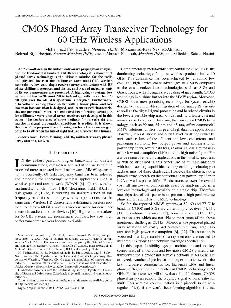
Fig. 1. (a) Simulated 3D view, and (b) top view of the propagation environment (CAD Lab at the University of Waterloo).
The organization of this paper is as follows. In Section II theindoor 60 GHz propagation channel is studied and a test set-upfor measuring the shadowing loss of a human body is described.A low-cost architecture for 60 GHz phased array transceiveris presented in Section III and the design, analysis and mea-surements of its key components are presented in Section IV.Finally, novel beamforming algorithms for the phased arrayreceiver are introduced in Section V and Section VI concludesthis paper.
II. INDOOR 60 GHz PROPAGATION CHANNEL: MODELING AND
MEASUREMENT
A. Modeling
Indoor propagation at MMW frequencies can be modeledusing geometrical optics (GO) ray-tracing method enhancedby uniform asymptotic diffraction theories and experimentalmodels. The reliability of channel characterization resultsobtained by ray-tracing method at microwave frequencieshas been confirmed by different measurements [16]–[18]. Forindoor applications at 60 GHz, the high penetration loss of thematerial isolates adjacent rooms and significantly limits thereceived interference, so only those objects inside the roomneed to be included in ray-tracing simulation. In this in-roompropagation channel, both line of sight (LOS) and non line ofsight (NLOS) rays must be considered. The NLOS rays arecaused by reflections from the objects inside the room as well assome significant first order diffracted rays. Furthermore, prop-agation loss in the ray-tracing modeling consists of free-spaceloss according to Friis formula, gaseous loss, and reflection,transmission and diffraction losses.
In this work, a 3D ray-tracing modeling (GO plus diffrac-tion) is employed to assess the signal coverage at 60 GHz fora regular office area. The CAD Laboratory, located in the EITbuilding at the University of Waterloo, is used as a typical in-door wireless environment (see Fig. 1(a)). The lab is furnishedwith tables, chairs and shelves mostly constructed of wooden
TABLE IMEASURED PERMITTIVITY OF INDOOR MATERIALS AT 60 GHz
and plastic material. The walls consist of layers of different ma-terial such as plasterboard, concrete, and wood. Moreover, var-ious electronic equipments such as computers, printers and testdevices are placed in this lab. The empirical data reported in [19]and [20] is used to calculate the reflection coefficients of the ma-terial. Moreover, to evaluate the human body shadowing effectthe measured permittivity data for biological tissues in [21] isused. Table I summarizes the measured permittivity data at 60GHz used in this work.
The transmitter antenna in Fig. 1 is located 10 cm below thecenter of the ceiling (facing down) which is 3.45 m above thefloor. The receiver is located on a wooden table 75 cm above thefloor. To simulate the shadowing effect, a human-body blocksthe LOS path between the transmitter and the receiver as shownin Fig. 1(b). To model a mobile user (portable end-device), thereceiver antenna moves within a 2 m 1.75 m grid located 1m above the floor (25 cm above the table). The resolution of thegrid-cells varies from to .
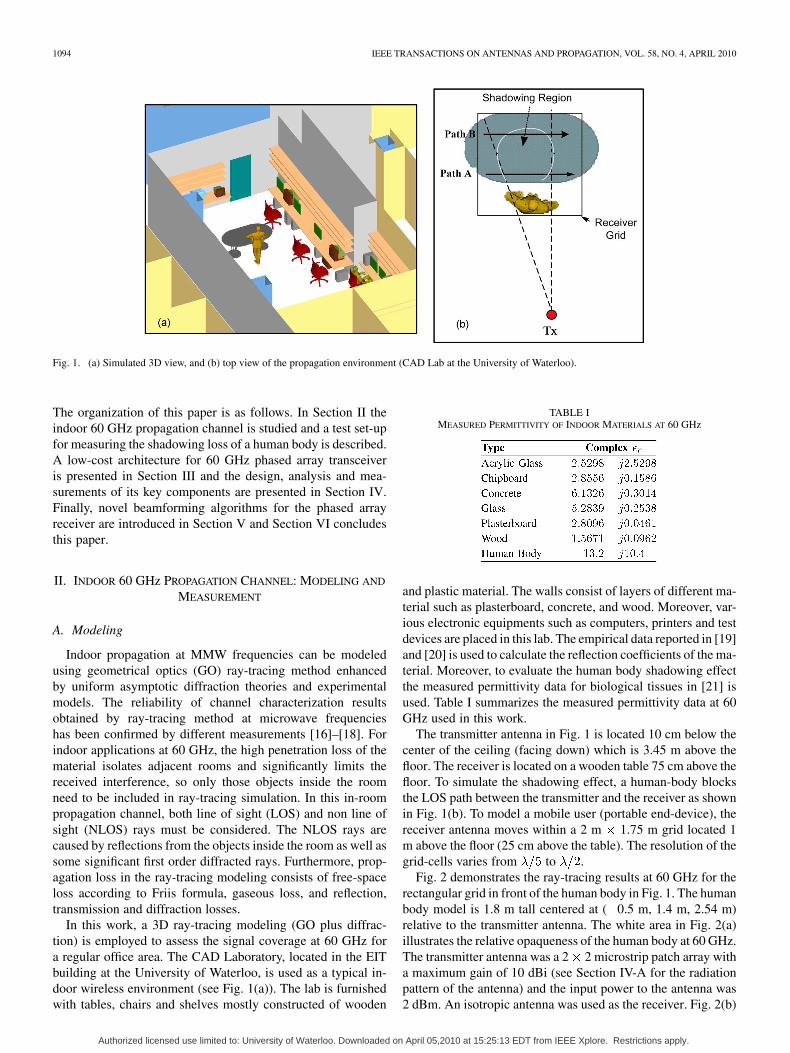
Fig. 2 demonstrates the ray-tracing results at 60 GHz for therectangular grid in front of the human body in Fig. 1. The humanbody model is 1.8 m tall centered at ( 0.5 m, 1.4 m, 2.54 m)relative to the transmitter antenna. The white area in Fig. 2(a)illustrates the relative opaqueness of the human body at 60 GHz.The transmitter antenna was a 2 2 microstrip patch array witha maximum gain of 10 dBi (see Section IV-A for the radiationpattern of the antenna) and the input power to the antenna was2 dBm. An isotropic antenna was used as the receiver. Fig. 2(b)
Authorized licensed use limited to: University of Waterloo. Downloaded on April 05,2010 at 15:25:13 EDT from IEEE Xplore. Restrictions apply.
FAKHARZADEH et al.: CMOS PHASED ARRAY TRANSCEIVER TECHNOLOGY FOR 60 GHz WIRELESS APPLICATIONS 1095
Fig. 2. (a) Received power over the rectangular grid in Fig. 1(b) around the human body. (b) Received power on Path A and Path B shown in Fig. 1(b).
shows the received power on two horizontal lines, named Path Aand Path B, in the region shown in Fig. 2(a). Path A and Path Bare respectively 20 cm and 80 cm in front of the human body and1.7 m and 2.3 m away from the projected transmitter position inFig. 1(b). The shadowing effect attenuates the received powerlevel by 10 to 40 dB for Path A and by 15 to 30 dB for Path B.The other objects in the room cause up to 5 dB fluctuationsin the received signal level. In calculating the received powerthe time-delay and phase of all rays, which their magnitudesare above 120 dBm, have been considered. This threshold isalmost 40 dB below the thermal noise power with 2.16 GHzequivalent bandwidth.
B. Measurements
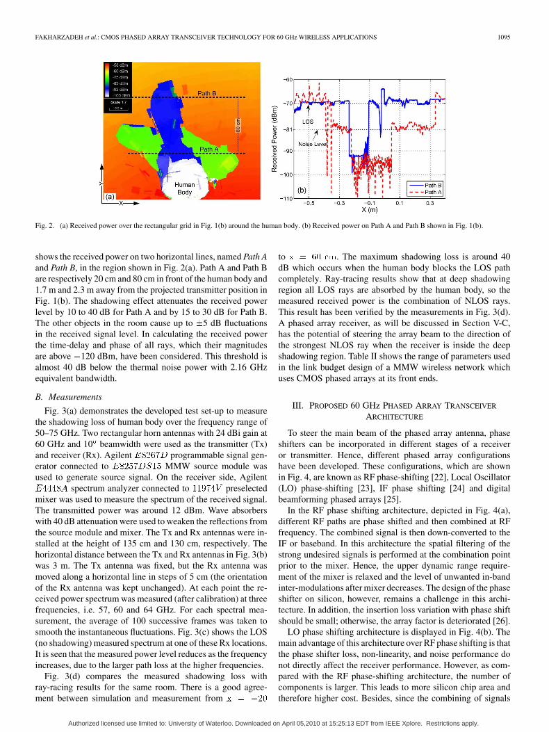
Fig. 3(a) demonstrates the developed test set-up to measurethe shadowing loss of human body over the frequency range of50–75 GHz. Two rectangular horn antennas with 24 dBi gain at60 GHz and 10 beamwidth were used as the transmitter (Tx)and receiver (Rx). Agilent programmable signal gen-erator connected to MMW source module wasused to generate source signal. On the receiver side, Agilent
spectrum analyzer connected to preselectedmixer was used to measure the spectrum of the received signal.The transmitted power was around 12 dBm. Wave absorberswith 40 dB attenuation were used to weaken the reflections fromthe source module and mixer. The Tx and Rx antennas were in-stalled at the height of 135 cm and 130 cm, respectively. Thehorizontal distance between the Tx and Rx antennas in Fig. 3(b)was 3 m. The Tx antenna was fixed, but the Rx antenna wasmoved along a horizontal line in steps of 5 cm (the orientationof the Rx antenna was kept unchanged). At each point the re-ceived power spectrum was measured (after calibration) at threefrequencies, i.e. 57, 60 and 64 GHz. For each spectral mea-surement, the average of 100 successive frames was taken tosmooth the instantaneous fluctuations. Fig. 3(c) shows the LOS(no shadowing) measured spectrum at one of these Rx locations.It is seen that the measured power level reduces as the frequencyincreases, due to the larger path loss at the higher frequencies.
Fig. 3(d) compares the measured shadowing loss withray-racing results for the same room. There is a good agree-ment between simulation and measurement from
to . The maximum shadowing loss is around 40dB which occurs when the human body blocks the LOS pathcompletely. Ray-tracing results show that at deep shadowingregion all LOS rays are absorbed by the human body, so themeasured received power is the combination of NLOS rays.This result has been verified by the measurements in Fig. 3(d).A phased array receiver, as will be discussed in Section V-C,has the potential of steering the array beam to the direction ofthe strongest NLOS ray when the receiver is inside the deepshadowing region. Table II shows the range of parameters usedin the link budget design of a MMW wireless network whichuses CMOS phased arrays at its front ends.
III. PROPOSED 60 GHz PHASED ARRAY TRANSCEIVER
ARCHITECTURE
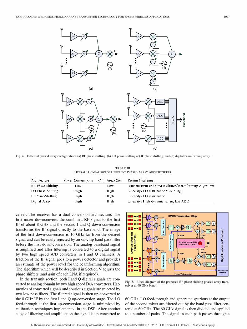
To steer the main beam of the phased array antenna, phaseshifters can be incorporated in different stages of a receiveror transmitter. Hence, different phased array configurationshave been developed. These configurations, which are shownin Fig. 4, are known as RF phase-shifting [22], Local Oscillator(LO) phase-shifting [23], IF phase shifting [24] and digitalbeamforming phased arrays [25].
In the RF phase shifting architecture, depicted in Fig. 4(a),different RF paths are phase shifted and then combined at RFfrequency. The combined signal is then down-converted to theIF or baseband. In this architecture the spatial filtering of thestrong undesired signals is performed at the combination pointprior to the mixer. Hence, the upper dynamic range require-ment of the mixer is relaxed and the level of unwanted in-bandinter-modulations after mixer decreases. The design of the phaseshifter on silicon, however, remains a challenge in this archi-tecture. In addition, the insertion loss variation with phase shiftshould be small; otherwise, the array factor is deteriorated [26].
LO phase shifting architecture is displayed in Fig. 4(b). Themain advantage of this architecture over RF phase shifting is thatthe phase shifter loss, non-linearity, and noise performance donot directly affect the receiver performance. However, as com-pared with the RF phase-shifting architecture, the number ofcomponents is larger. This leads to more silicon chip area andtherefore higher cost. Besides, since the combining of signals
Authorized licensed use limited to: University of Waterloo. Downloaded on April 05,2010 at 15:25:13 EDT from IEEE Xplore. Restrictions apply.
1096 IEEE TRANSACTIONS ON ANTENNAS AND PROPAGATION, VOL. 58, NO. 4, APRIL 2010
Fig. 3. Measurement environment and results. (a) Test set-up with transmitter and receiver. (b) Tx and Rx antenna locations in the room. (c) One sample of themeasured spectrum at 57, 60 and 64 GHz. (d) Comparison of the measured and simulation results.
TABLE IILINK-BUDGET DESIGN FOR A 60 GHz WIRELESS NETWORK USING CMOS
TECHNOLOGY
and beamforming are performed after mixers, in-band intermod-ulations are stronger. Also the upper dynamic range of the mixermust be high enough to stand strong interference signals.
Fig. 4(c) shows the IF phase shifting architecture. The phaseshifters are placed at the first IF stage. The phase-shifted IF sig-nals are combined before downconversion to baseband. As com-pared to RF phase shifting architecture, some of the challenges
in phase shifter design are relaxed. However, since it needs mul-tiple mixers, this architecture is not a proper option for low costand low power phased array transceiver. Fig. 4(d) illustratesdigital array architecture. Down-converted to a suitable IF fre-quency, each RF path is digitized by an analog-to-digital con-verter (ADC) and all outputs are passed to a digital signal pro-cessing (DSP) unit, which executes all tasks of beamformingand recovering the desired signal from the undesired interfer-ences. The dynamic ranges of mixers and ADCs must be highenough to withstand the probable strong interferences. In case ofWPAN since the data rate may exceed 2 Gb/s, very high-speedADC’s are required and to accommodate the required dynamicrange each ADC must have a large number of bits which in-creases the ADC cost and power consumption extensively.
Table III summarizes the comparison of different phasedarray architectures in terms of power consumption, chip areaand design challenges. To overcome the high path loss andshadowing loss at 60 GHz as well as CMOS output power andnoise figure limitations multiple antennas and phase shifters arerequired. Considering Table III, the most appropriate config-uration to lower the cost and power consumption and achievea compact CMOS phased array transceiver is the RF phaseshifting architecture. However, designing an efficient front-endas well as developing fast, efficient beamforming algorithmsare the keys to overcome the phase shifter non-idealities andchallenges in RF path. Fig. 5 demonstrates the proposed blockdiagram of an RF phase shifting 60 GHz phased array trans-
Authorized licensed use limited to: University of Waterloo. Downloaded on April 05,2010 at 15:25:13 EDT from IEEE Xplore. Restrictions apply.
FAKHARZADEH et al.: CMOS PHASED ARRAY TRANSCEIVER TECHNOLOGY FOR 60 GHz WIRELESS APPLICATIONS 1097
Fig. 4. Different phased array configurations (a) RF phase shifting, (b) LO phase shifting (c) IF phase shifting, and (d) digital beamforming array.
TABLE IIIOVERALL COMPARISON OF DIFFERENT PHASED ARRAY ARCHITECTURES
ceiver. The receiver has a dual conversion architecture. Thefirst mixer downconverts the combined RF signal to the firstIF of about 8 GHz and the second I and Q down-conversiontransforms the IF signal directly to the baseband. The imageof the first down-conversion is 16 GHz far from the desiredsignal and can be easily rejected by an on-chip band pass filterbefore the first down-conversion. The analog baseband signalis amplified and after filtering is converted to a digital signalby two high speed A/D converters in I and Q channels. Afraction of the IF signal goes to a power detector and providesan estimate of the power level for the beamforming algorithm.The algorithm which will be described in Section V adjusts thephase shifters (and gain of each LNA if required).
In the transmit section, both I and Q digital signals are con-verted to analog domain by two high speed D/A converters. Har-monics of converted signals and spurious signals are rejected bytwo low pass filters. The filtered signal is then up-converted tothe 8 GHz IF by the first I and Q up-conversion stage. The LOfeed-through at the first up-conversion stage is minimized bycalibration techniques implemented in the DSP. After anotherstage of filtering and amplification the signal is up-converted to
Fig. 5. Block diagram of the proposed RF phase shifting phased array trans-ceiver at 60 GHz band.
60 GHz. LO feed-through and generated spurious at the outputof the second mixer are filtered out by the band pass filter cen-tered at 60 GHz. The 60 GHz signal is then divided and appliedto a number of paths. The signal in each path passes through a
Authorized licensed use limited to: University of Waterloo. Downloaded on April 05,2010 at 15:25:13 EDT from IEEE Xplore. Restrictions apply.
1098 IEEE TRANSACTIONS ON ANTENNAS AND PROPAGATION, VOL. 58, NO. 4, APRIL 2010
Fig. 6. Configuration and radiation pattern of two designs for 2 � 2 patch arrays. (a) The maximum gain design. (b) The maximum beamwidth design. (c)Reflection coefficients of the patch arrays.
phase shifter block. The phase shifted signals are then amplifiedby power amplifier (PA) stages and applied to the transmit an-tenna array. The saturated output power of a 90 nm CMOS PAis around 10 dBm but to accommodate sufficient linearity forthe complex amplitude sensitive modulations such as QAM, theoutput power of power amplifier is set to 2 dBm to keep the PAin its linear operation region.
IV. DESIGN AND MEASUREMENT OF 60 GHz PHASED ARRAY
COMPONENTS
In this section the design and analysis of the key componentsof a 60 GHz phased array receiver, namely antenna element,LNA and phase shifter, are described, and measured results forLNA and phase shifter are presented.
A. Off-Chip Wide-Beam Antenna Design
A substantial body of research on millimeter-wave antennahas been conducted [2], [27]–[30]. For fixed wireless access(FWA) applications, a high gain antenna is preferred to relaxthe performance requirements of the front-end elements. A highgain antenna has a narrow beam. Thus, for mobile applications,where a wide antenna coverage is required (see Table II), asingle high-gain antenna is not an appropriate choice. ForMMW wireless networking applications ,assuming the base station has been located at the center ofthe ceiling, almost 2.5 m above the user, the antenna beamcoverage should be greater than to cover the whole areaof a room or office. A wide beam coverage and a high radiationgain cannot be achieved at the same time unless a phased arrayantenna with beam steering capability is used. Even in thiscase the 3 dB beamwidth of each array element must be morethan 65 to limit the beam steering loss. For this beamwidth theelement gain is limited to 10.2 dBi [31]. Thus, designing the
appropriate antenna element for 60 GHz WPAN is a delicatetask.
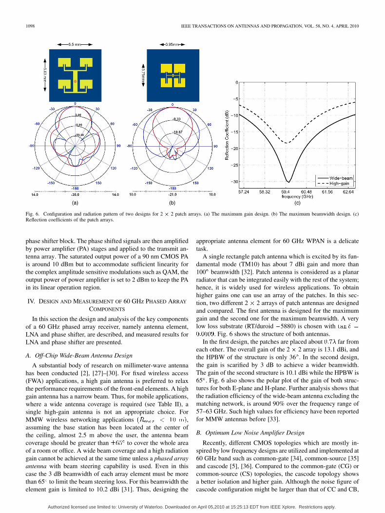
A single rectangle patch antenna which is excited by its fun-damental mode (TM10) has about 7 dBi gain and more than100 beamwidth [32]. Patch antenna is considered as a planarradiator that can be integrated easily with the rest of the system;hence, it is widely used for wireless applications. To obtainhigher gains one can use an array of the patches. In this sec-tion, two different 2 2 arrays of patch antennas are designedand compared. The first antenna is designed for the maximumgain and the second one for the maximum beamwidth. A verylow loss substrate (RT/duroid 5880) is chosen with
. Fig. 6 shows the structure of both antennas.In the first design, the patches are placed about far from
each other. The overall gain of the 2 2 array is 13.1 dBi, andthe HPBW of the structure is only 36 . In the second design,the gain is scarified by 3 dB to achieve a wider beamwidth.The gain of the second structure is 10.1 dBi while the HPBW is65 . Fig. 6 also shows the polar plot of the gain of both struc-tures for both E-plane and H-plane. Further analysis shows thatthe radiation efficiency of the wide-beam antenna excluding thematching network, is around 90% over the frequency range of57–63 GHz. Such high values for efficiency have been reportedfor MMW antennas before [33].
B. Optimum Low Noise Amplifier Design
Recently, different CMOS topologies which are mostly in-spired by low frequency designs are utilized and implemented at60 GHz band such as common-gate [34], common-source [35]and cascode [5], [36]. Compared to the common-gate (CG) orcommon-source (CS) topologies, the cascode topology showsa better isolation and higher gain. Although the noise figure ofcascode configuration might be larger than that of CC and CB,
Authorized licensed use limited to: University of Waterloo. Downloaded on April 05,2010 at 15:25:13 EDT from IEEE Xplore. Restrictions apply.
FAKHARZADEH et al.: CMOS PHASED ARRAY TRANSCEIVER TECHNOLOGY FOR 60 GHz WIRELESS APPLICATIONS 1099
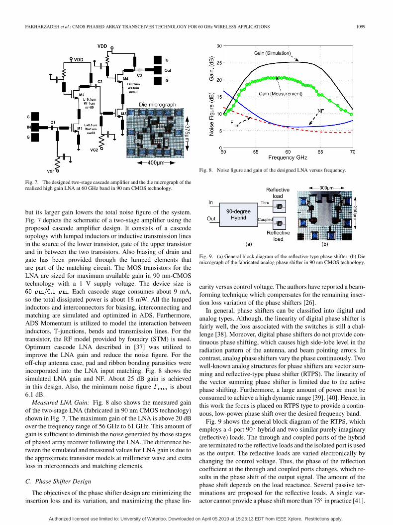
Fig. 7. The designed two-stage cascade amplifier and the die micrograph of therealized high gain LNA at 60 GHz band in 90 nm CMOS technology.
but its larger gain lowers the total noise figure of the system.Fig. 7 depicts the schematic of a two-stage amplifier using theproposed cascode amplifier design. It consists of a cascodetopology with lumped inductors or inductive transmission linesin the source of the lower transistor, gate of the upper transistorand in between the two transistors. Also biasing of drain andgate has been provided through the lumped elements thatare part of the matching circuit. The MOS transistors for theLNA are sized for maximum available gain in 90 nm-CMOStechnology with a 1 V supply voltage. The device size is
. Each cascode stage consumes about 9 mA,so the total dissipated power is about 18 mW. All the lumpedinductors and interconnectors for biasing, interconnecting andmatching are simulated and optimized in ADS. Furthermore,ADS Momentum is utilized to model the interaction betweeninductors, T-junctions, bends and transmission lines. For thetransistor, the RF model provided by foundry (STM) is used.Optimum cascode LNA described in [37] was utilized toimprove the LNA gain and reduce the noise figure. For theoff-chip antenna case, pad and ribbon bonding parasitics wereincorporated into the LNA input matching. Fig. 8 shows thesimulated LNA gain and NF. About 25 dB gain is achievedin this design. Also, the minimum noise figure is about6.1 dB.
Measured LNA Gain: Fig. 8 also shows the measured gainof the two-stage LNA (fabricated in 90 nm CMOS technology)shown in Fig. 7. The maximum gain of the LNA is above 20 dBover the frequency range of 56 GHz to 61 GHz. This amount ofgain is sufficient to diminish the noise generated by those stagesof phased array receiver following the LNA. The difference be-tween the simulated and measured values for LNA gain is due tothe approximate transistor models at millimeter wave and extraloss in interconnects and matching elements.
C. Phase Shifter Design
The objectives of the phase shifter design are minimizing theinsertion loss and its variation, and maximizing the phase lin-
Fig. 8. Noise figure and gain of the designed LNA versus frequency.
Fig. 9. (a) General block diagram of the reflective-type phase shifter. (b) Diemicrograph of the fabricated analog phase shifter in 90 nm CMOS technology.
earity versus control voltage. The authors have reported a beam-forming technique which compensates for the remaining inser-tion loss variation of the phase shifters [26].
In general, phase shifters can be classified into digital andanalog types. Although, the linearity of digital phase shifter isfairly well, the loss associated with the switches is still a chal-lenge [38]. Moreover, digital phase shifters do not provide con-tinuous phase shifting, which causes high side-lobe level in theradiation pattern of the antenna, and beam pointing errors. Incontrast, analog phase shifters vary the phase continuously. Twowell-known analog structures for phase shifters are vector sum-ming and reflective-type phase shifter (RTPS). The linearity ofthe vector summing phase shifter is limited due to the activephase shifting. Furthermore, a large amount of power must beconsumed to achieve a high dynamic range [39], [40]. Hence, inthis work the focus is placed on RTPS type to provide a contin-uous, low-power phase shift over the desired frequency band.
Fig. 9 shows the general block diagram of the RTPS, whichemploys a 4-port 90 -hybrid and two similar purely imaginary(reflective) loads. The through and coupled ports of the hybridare terminated to the reflective loads and the isolated port is usedas the output. The reflective loads are varied electronically bychanging the control voltage. Thus, the phase of the reflectioncoefficient at the through and coupled ports changes, which re-sults in the phase shift of the output signal. The amount of thephase shift depends on the load reactance. Several passive ter-minations are proposed for the reflective loads. A single var-actor cannot provide a phase shift more than 75 in practice [41].
Authorized licensed use limited to: University of Waterloo. Downloaded on April 05,2010 at 15:25:13 EDT from IEEE Xplore. Restrictions apply.
1100 IEEE TRANSACTIONS ON ANTENNAS AND PROPAGATION, VOL. 58, NO. 4, APRIL 2010
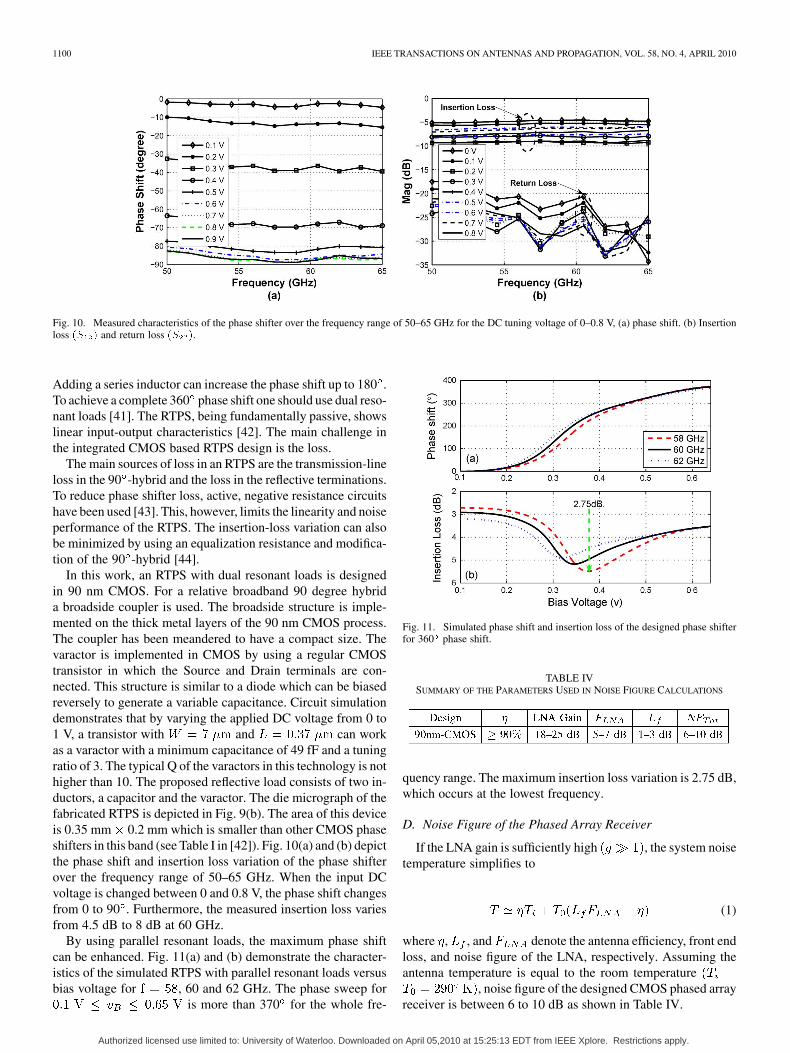
Fig. 10. Measured characteristics of the phase shifter over the frequency range of 50–65 GHz for the DC tuning voltage of 0–0.8 V, (a) phase shift. (b) Insertionloss �� � and return loss �� �.
Adding a series inductor can increase the phase shift up to 180 .To achieve a complete 360 phase shift one should use dual reso-nant loads [41]. The RTPS, being fundamentally passive, showslinear input-output characteristics [42]. The main challenge inthe integrated CMOS based RTPS design is the loss.
The main sources of loss in an RTPS are the transmission-lineloss in the 90 -hybrid and the loss in the reflective terminations.To reduce phase shifter loss, active, negative resistance circuitshave been used [43]. This, however, limits the linearity and noiseperformance of the RTPS. The insertion-loss variation can alsobe minimized by using an equalization resistance and modifica-tion of the 90 -hybrid [44].
In this work, an RTPS with dual resonant loads is designedin 90 nm CMOS. For a relative broadband 90 degree hybrida broadside coupler is used. The broadside structure is imple-mented on the thick metal layers of the 90 nm CMOS process.The coupler has been meandered to have a compact size. Thevaractor is implemented in CMOS by using a regular CMOStransistor in which the Source and Drain terminals are con-nected. This structure is similar to a diode which can be biasedreversely to generate a variable capacitance. Circuit simulationdemonstrates that by varying the applied DC voltage from 0 to1 V, a transistor with and can workas a varactor with a minimum capacitance of 49 fF and a tuningratio of 3. The typical Q of the varactors in this technology is nothigher than 10. The proposed reflective load consists of two in-ductors, a capacitor and the varactor. The die micrograph of thefabricated RTPS is depicted in Fig. 9(b). The area of this deviceis 0.35 mm 0.2 mm which is smaller than other CMOS phaseshifters in this band (see Table I in [42]). Fig. 10(a) and (b) depictthe phase shift and insertion loss variation of the phase shifterover the frequency range of 50–65 GHz. When the input DCvoltage is changed between 0 and 0.8 V, the phase shift changesfrom 0 to 90 . Furthermore, the measured insertion loss variesfrom 4.5 dB to 8 dB at 60 GHz.
By using parallel resonant loads, the maximum phase shiftcan be enhanced. Fig. 11(a) and (b) demonstrate the character-istics of the simulated RTPS with parallel resonant loads versusbias voltage for , 60 and 62 GHz. The phase sweep for
is more than 370 for the whole fre-
Fig. 11. Simulated phase shift and insertion loss of the designed phase shifterfor 360 phase shift.
TABLE IVSUMMARY OF THE PARAMETERS USED IN NOISE FIGURE CALCULATIONS
quency range. The maximum insertion loss variation is 2.75 dB,which occurs at the lowest frequency.
D. Noise Figure of the Phased Array Receiver
If the LNA gain is sufficiently high , the system noisetemperature simplifies to
(1)
where , , and denote the antenna efficiency, front endloss, and noise figure of the LNA, respectively. Assuming theantenna temperature is equal to the room temperature
, noise figure of the designed CMOS phased arrayreceiver is between 6 to 10 dB as shown in Table IV.
Authorized licensed use limited to: University of Waterloo. Downloaded on April 05,2010 at 15:25:13 EDT from IEEE Xplore. Restrictions apply.
FAKHARZADEH et al.: CMOS PHASED ARRAY TRANSCEIVER TECHNOLOGY FOR 60 GHz WIRELESS APPLICATIONS 1101
V. BEAMFORMING
In this section, two novel beamforming algorithms for theMMW receiver phased array antenna are proposed, and theachieved improvement in the signal to noise ratio at the arrayoutput is presented.
A. Beamforming Algorithms for MMW Receiver Phased Array
The goal of the beamforming algorithm is to increase thearray factor and consequently provide the SNR determined byBit Error Rate (BER) constrains. The ideal limit of the arrayfactor is equal to the number of array elements; however, as itwill be shown, the practical maximum array factor is smallerthan that due to the variable insertion loss of phase shifter.
1) Signal Model: Let denotethe received signals by all elements of the array. Then it con-sists of three parts: source signal , interference , andbackground noise ,
(2)
The background noise is assumed to be spatially white. Assumethe source (transmitter) is located at direction inthe receiver array coordinate system, transmitting RF signals atfrequency . The RF signal received by an element of the arraylocated at is given by
(3)
where , and are respectively the RF wave numberand the source waveform. The path loss is included in .The array output for a single receiver array structure shown inFig. 4(a) is
(4)
where is the array weights vector and denotes the Hermi-tian operator. If analog phase shifters, such as the one shown inFig. 11, were used to adjust the array weights for beamformingthe wight vector would be [45]
(5)
where is the control voltage of the phase shifter, and anddenote the amplitude (insertion loss) and phase-shift functions
of the phase shifter. The total received power by the array is then
(6)
2) Statement of the Problem: In the absence of co-channelinterference, beamforming for a MMW receiver array is a con-strained optimization problem with the objective of maximizing
the total received power by the array. The voltage dependentcharacteristics of the phase shifters form the constrains of theoptimization problem. Hence, the beamforming problem can bestated as
(7)
In [45], [46], the authors have shown that an efficient way tosolve this problem is to use a gradient estimation approach suchas zero-knowledge beamforming algorithm. In this case the con-trol voltages are updated in an iterative manner
(8)
where is an internal algorithm parameter called the step size,and is the gradient of power with respect to . Sincethe exact calculation of the gradient is not practical it is replacedby an estimated vector:
(9)
where each component is the approximate partial deriva-tive of w.r.t. .
3) Reverse-Channel Aided Beamforming: The size and costconstrains of the 60 GHz receiver do not allow for incorpo-rating a complex processor in the portable node. However, theaccess point (fixed node) can handle more elaborate signal pro-cessing tasks. Moreover, in MMW networking standards suchas WPAN, 50 MHz of the spectrum is reserved for the reversechannel to carry the control signals between the access pointsand mobile nodes. Access point can be equipped with direc-tion-of arrival (DOA) estimation unit. This unit can calculatethe relative position of the mobile nodes and send this informa-tion to them. The mobile node can use this information to adjustits beam. Although this method is very fast, in the case of shad-owing it is not efficient. In this case the beamformer must beable to maintain the array beam on the direction of the strongestcomponent of the multipath signal.
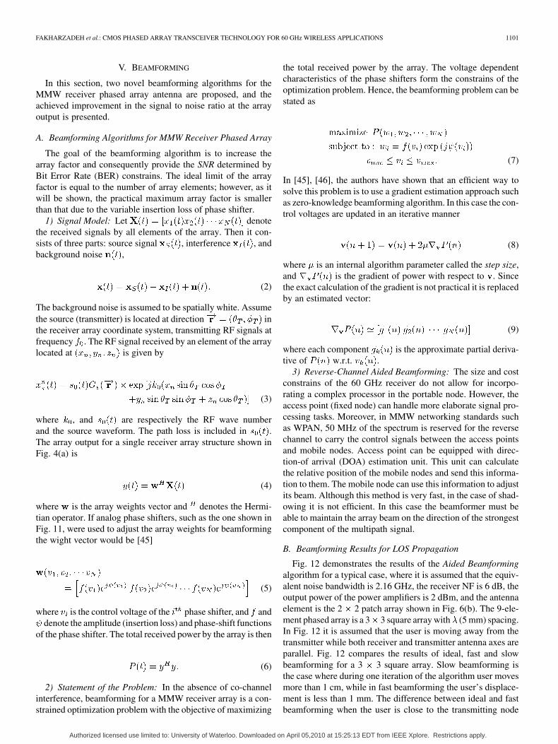
B. Beamforming Results for LOS Propagation
Fig. 12 demonstrates the results of the Aided Beamformingalgorithm for a typical case, where it is assumed that the equiv-alent noise bandwidth is 2.16 GHz, the receiver NF is 6 dB, theoutput power of the power amplifiers is 2 dBm, and the antennaelement is the 2 2 patch array shown in Fig. 6(b). The 9-ele-ment phased array is a 3 3 square array with (5 mm) spacing.In Fig. 12 it is assumed that the user is moving away from thetransmitter while both receiver and transmitter antenna axes areparallel. Fig. 12 compares the results of ideal, fast and slowbeamforming for a 3 3 square array. Slow beamforming isthe case where during one iteration of the algorithm user movesmore than 1 cm, while in fast beamforming the user’s displace-ment is less than 1 mm. The difference between ideal and fastbeamforming when the user is close to the transmitting node
Authorized licensed use limited to: University of Waterloo. Downloaded on April 05,2010 at 15:25:13 EDT from IEEE Xplore. Restrictions apply.
1102 IEEE TRANSACTIONS ON ANTENNAS AND PROPAGATION, VOL. 58, NO. 4, APRIL 2010
Fig. 12. Received SNR by a 3 � 3 square phased array antenna for differentbeamforming scenarios.
m is 2 dB. As the distance increases to thisdifference raises to more than 3.5 dB.
Another important result of Fig. 12 is that the beamforminggain depends on the received power. So, as the distance be-tween the portable receiver and the transmitting node increases,the performance of the beamforming degrades. Moreover, thebeamforming speed affects the beamforming gain. A similarversion of this algorithm has been successfully applied to a 34element Ku-band phase array antenna [46]. The duration of eachbeamforming iteration was measured to be less than 5 ms witha 125 KHz Digital-to-Analog convertor.
C. Beamforming Results for NLOS Propagation
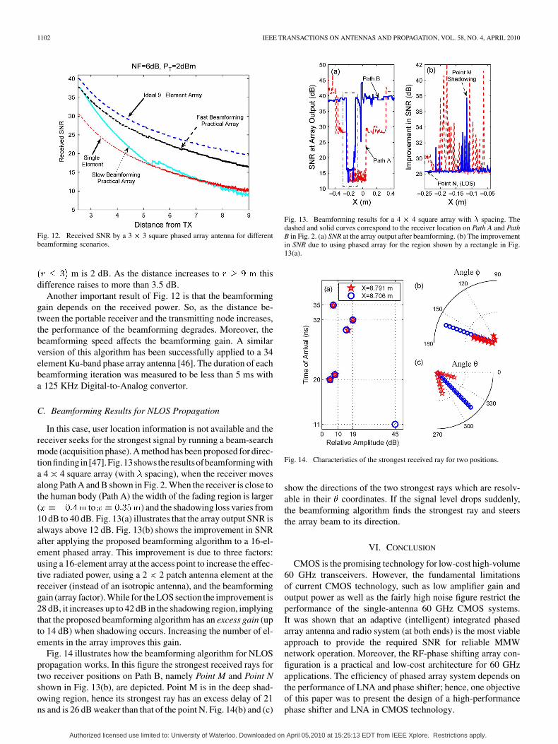
In this case, user location information is not available and thereceiver seeks for the strongest signal by running a beam-searchmode (acquisition phase). A method has been proposed for direc-tionfindingin[47].Fig.13showstheresultsofbeamformingwitha 4 4 square array (with spacing), when the receiver movesalong Path A and B shown in Fig. 2. When the receiver is close tothe human body (Path A) the width of the fading region is larger( to ) and the shadowing loss varies from10 dB to 40 dB. Fig. 13(a) illustrates that the array output SNR isalways above 12 dB. Fig. 13(b) shows the improvement in SNRafter applying the proposed beamforming algorithm to a 16-el-ement phased array. This improvement is due to three factors:using a 16-element array at the access point to increase the effec-tive radiated power, using a 2 2 patch antenna element at thereceiver (instead of an isotropic antenna), and the beamforminggain (array factor). While for the LOS section the improvement is28 dB, it increases up to 42 dB in the shadowing region, implyingthat the proposed beamforming algorithm has an excess gain (upto 14 dB) when shadowing occurs. Increasing the number of el-ements in the array improves this gain.
Fig. 14 illustrates how the beamforming algorithm for NLOSpropagation works. In this figure the strongest received rays fortwo receiver positions on Path B, namely Point M and Point Nshown in Fig. 13(b), are depicted. Point M is in the deep shad-owing region, hence its strongest ray has an excess delay of 21ns and is 26 dB weaker than that of the point N. Fig. 14(b) and (c)
Fig. 13. Beamforming results for a 4 � 4 square array with � spacing. Thedashed and solid curves correspond to the receiver location on Path A and PathB in Fig. 2. (a) SNR at the array output after beamforming. (b) The improvementin SNR due to using phased array for the region shown by a rectangle in Fig.13(a).
Fig. 14. Characteristics of the strongest received ray for two positions.
show the directions of the two strongest rays which are resolv-able in their coordinates. If the signal level drops suddenly,the beamforming algorithm finds the strongest ray and steersthe array beam to its direction.
VI. CONCLUSION
CMOS is the promising technology for low-cost high-volume60 GHz transceivers. However, the fundamental limitationsof current CMOS technology, such as low amplifier gain andoutput power as well as the fairly high noise figure restrict theperformance of the single-antenna 60 GHz CMOS systems.It was shown that an adaptive (intelligent) integrated phasedarray antenna and radio system (at both ends) is the most viableapproach to provide the required SNR for reliable MMWnetwork operation. Moreover, the RF-phase shifting array con-figuration is a practical and low-cost architecture for 60 GHzapplications. The efficiency of phased array system depends onthe performance of LNA and phase shifter; hence, one objectiveof this paper was to present the design of a high-performancephase shifter and LNA in CMOS technology.
Authorized licensed use limited to: University of Waterloo. Downloaded on April 05,2010 at 15:25:13 EDT from IEEE Xplore. Restrictions apply.
FAKHARZADEH et al.: CMOS PHASED ARRAY TRANSCEIVER TECHNOLOGY FOR 60 GHz WIRELESS APPLICATIONS 1103
To design the link budget for 60 GHz network, the propaga-tion of the MMW signal in an indoor environment was studiedfor LOS and NLOS scenarios, and verified by measurements.It was found that the shadowing loss of a human body can beas high as 40 dB. In this case all LOS rays are absorbed by thehuman body and only NLOS rays are received.
A low noise amplifier using cascode topology, was designedand fabricated in 90 nm CMOS technology. The measured gainof this two stage LNA exceeded 20 dB at the frequency rangeof 56–61 GHz. Furthermore, to meet the beamforming require-ments, a broadband reflective type phase shifter in 90 nm CMOSwith a linear phase and low insertion loss, was designed, fabri-cated and successfully tested.
Finally, a fast beamforming algorithm was developed to re-alize the potentials of phased array for both LOS and multi-path signal propagation. The imbalanced insertion loss of phaseshifters results in a margin between the ideal and practical arraygain, which reduces the effective range or transmitted/receivedpower by the array. Moreover, the beamforming gain is pro-portional to the input SNR. In the case of shadowing, the pro-posed beamforming algorithm seeks for the strongest ray. Itwas shown an excess gain up to 14 dB can be obtained by thismethod.
ACKNOWLEDGMENT
The authors would like to acknowledge CMC (Canadian Mi-croelectronics Corporation) for device fabrication. The authorsare thankful to Mr. J. Dietrich at CMC Advanced RF Lab at theUniversity of Manitoba for on-wafer measurements, and Mr. H.Mirzaei.
REFERENCES
[1] K. Ohata et al., “Sixty-GHz-band ultra-miniature monolithic T/R mod-ules for multimedia wireless communication systems,” IEEE Trans.Microw. Theory Tech., vol. 44, no. 12, pp. 2354–2360, Dec. 1996.
[2] S. Reynolds et al., “A silicon 60 GHz receiver and transmitter chipsetfor broadband communications,” IEEE J. Solid-State Circuits, vol. 41,no. 12, pp. 2820–2830, Dec. 2006.
[3] S. E. Gunnarsson et al., “60 GHz single-chip front-end MMICs andsystems for multi-Gb/s wireless communication,” IEEE J. Solid-StateCircuits, vol. 42, no. 5, pp. 1143–1157, May 2007.
[4] T. Mitomo et al., “A 60-GHz CMOS receiver front-end with fre-quency synthesizer,” IEEE J. Solid-State Circuits, vol. 43, no. 4, pp.1030–1037, Apr. 2008.
[5] C. H. Doan, S. Emami, A. M. Niknejad, and R. W. Brodersen, “Mil-limeter-wave CMOS design,” IEEE J. Solid-State Circuits, vol. 40, no.1, pp. 144–155, Jan. 2005.
[6] A. Babakhani et al., “A 77-GHz phased-array transceiver with on-chipantennas in silicon: Receiver and antennas,” IEEE J. Solid-State Cir-cuits, vol. 41, no. 12, pp. 2795–2806, Dec. 2006.
[7] B. Razavi, “Gadgets gab at 60 GHz,” IEEE Spectrum, vol. 45, no. 2,pp. 46–58, Feb. 2008.
[8] P. Smulders, “Exploiting the 60 GHz band for local wireless multi-media access: Prospects and future directions,” Commun. Mag., IEEE,vol. 40, no. 1, pp. 140–147, Jan. 2002.
[9] C. Park and T. Rappaport, “Short-range wireless communications fornext-generation networks: UWB, 60 GHz millimeter-wave WPAN, andZigBee,” IEEE Wireless Commun., vol. 14, no. 4, pp. 70–78, Aug.2007.
[10] Wirelesshd Specification Version 1.0 Overview 2007 [Online].Available: http://www.wirelesshd.org/WirelessHD-Full-Overview-071009.pdf
[11] B. Razavi, “A 60-GHz CMOS receiver front-end,” IEEE J. Solid-StateCircuits, vol. 41, no. 1, pp. 17–22, Jan. 2006.
[12] K. Scheir, S. Bronckers, J. Borremans, P. Wambacq, and Y. Rolain, “A52 GHz phased-array receiver front-end in 90 nm digital CMOS,” IEEEJ. Solid-State Circuits, vol. 43, no. 12, pp. 2651–2659, Dec. 2008.
[13] S. R. Alberto Valdes-Garcia and J.-O. Plouchart, “60 GHz transmittercircuits in 65 nm CMOS,” in Proc. IEEE Radio Frequency IntegratedCircuits Symp., Jun. 2008, pp. 641–644.
[14] A. P. M. Boers and N. Weste, “A 60 GHz transmitter in 0.18 �� sil-icon germanium,” in Proc. Wireless Broadband and Ultra WidebandCommunications, Aug. 27–30, 2007, p. 36.
[15] B. Razavi, “CMOS transceivers for the 60-GHz band,” presented at theIEEE Radio Frequency Integrated Circuits Symp., Jun. 2006.
[16] T. Manabe, Y. Miura, and T. Ihara, “Effects of antenna directivityand polarization on indoor multipath propagation characteristics at 60GHz,” IEEE J. Selec. Area Commun., vol. 14, no. 3, pp. 1441–1448,Apr. 1996.
[17] C.-P. Lim, M. Lee, R. J. Burkholder, J. L. Volakis, and R. J. Marhefka,“60 GHz indoor propagation studies for wireless communicationsbased on a Ray-tracing method,” EURASIP J. Wireless Commun. Net.,2007, article ID 73928.
[18] P. F. M. Smulders, C. F. Li, H. Yang, E. F. T. Martijn, and M. H. A.J. Herben, “60 GHz indoor radio propagation—Comparison of simu-lation and measurement results,” presented at the IEEE 11th Symp. onCommun. and Veh. Technol., 2004.
[19] B. Langen, G. Lober, and W. Herzig, “Reflection and transmission be-haviour of building materials at 60 GHZ,” in Proc. IEEE Int. Symp.Personal, Indoor and Mobile Radio Commun., 1994, pp. 505–509.
[20] L. M. Correia and P. O. Frances, “Estimation of materials characteris-tics from power measurements at 60 GHz,” in Proc. IEEE Int. Symp.Personal, Indoor and Mobile Radio Commun., 1994, pp. 510–513.
[21] C. M. Alabaster, “Permittivity of human skin in millimetre wave band,”Electron. Lett., vol. 39, no. 21, pp. 1521–1522, Oct. 2003, article ID73928.
[22] R. J. Mailloux, Phased Array Antenna Handbook—Chapter 1, 2nded. Boston, MA: Artech House, 2005.
[23] H. Hashemi, X. Guan, A. Komijani, and A. Hajimiri, “A 24-GHz SiGephased-array receiver LO phase-shifting approach,” IEEE Trans. Mi-crow. Theory Tech., vol. 53, no. 2, pp. 614–626, Feb. 2005.
[24] S. Raman, N. Barker, and G. Rebeiz, “A w-band dielectric-lens-basedintegrated monopulse radar receiver,” IEEE Trans. Microw. TheoryTech., vol. 46, no. 12, pp. 2308–2316, Dec. 1998.
[25] R. Miura, T. Tanaka, I. Chiba, A. Horie, and Y. Karasawa, “Beam-forming experiment with a DBF multibeam antenna in a mobile satel-lite environment,” IEEE Trans. Antennas Propag., vol. 45, no. 4, pp.707–714, Apr. 1997.
[26] M. Fakharzadeh, P. Mousavi, S. Safavi-Naeini, and S. H. Jamali, “Theeffects of imbalanced phase shifters loss on phased array gain,” IEEEAntennas Wireless Propag. Lett., vol. 7, pp. 192–196.
[27] T. Zwick, D. Liu, and B. P. Gaucher, “Broadband planar superstrateantenna for integrated millimeterwave transceivers,” IEEE Trans. An-tennas Propag., vol. 54, no. 10, pp. 2790–2796, Oct. 2006.
[28] E. Ojefors, H. Kratz, K. Grenier, R. Plana, and A. Rydberg, “Microma-chined loop antennas on low resistivity silicon substrates,” IEEE Trans.Antennas Propag., vol. 54, no. 12, pp. 3593–3601, Dec. 2006.
[29] C. Karnfelt, P. Hallbjorner, H. Zirath, and A. Alping, “High gain ac-tive microstrip antenna for 60-GHz WLAN/WPAN applications,” IEEETrans. Microw. Theory Tech., vol. 54, no. 6, pt. 2, pp. 2593–2603, Jun.2006.
[30] A. Lamminen, J. Saily, and A. R. Vimpari, “60-GHz patch antennasand arrays on LTCC with embedded-cavity substrates,” IEEE Trans.Antennas Propag., vol. 56, no. 9, pp. 2865–2874, Sep. 2006.
[31] R. C. Johnson and H. Jasik, Antenna Engineering Handbook. NewYork: McGraw-Hill, 1961.
[32] J. R. James and P. S. Hall, Handbook of Microstrip Antennas.London, U.K.: Inst. Elec. Eng., 1989.
[33] R. A. Alhalabi and G. M. Rebeiz, “High-efficiency angled-dipole an-tennas for millimeter-wave phased array applications,” IEEE Trans.Antennas Propag., vol. 56, no. 10, pp. 3136–3142, Oct. 2008.
[34] B. Razavi, “A 60-GHz direct-conversion CMOS receiver,” in IEEEISSCC. Proc., Feb. 2005, pp. 400–401.
[35] B. Heydari, P. Reynaert, E. Adabi, M. Bohsali, B. Afshar, M. A.Arbabian, and A. M. Niknejad, “A 60-GHz 90-nm CMOS cascodeamplifier with interstage matching,” IEEE J. Solid-State Circuits, vol.42, no. 12, pp. 2893–2904, Dec. 2007.
[36] C.-M. Lo, C.-S. Lin, and H. Wang, “A miniature V-band 3-stage cas-code LNA in 0.13 �� CMOS,” in IEEE ISSCC Dig. Tech. Papers, Feb.2006, pp. 322–323.
[37] M. R. Nezhad Ahmadi, B. Biglarbegian, H. Mirzaei, and S. Safavi-Naeini, “An optimum cascode topology for high gain micro/millimeterwave CMOS amplifier design,” in Proc. Eur. Microwave IntegratedCircuit Conf. (EuMIC), Netherlands, Oct. 2008, pp. 394–397.
Authorized licensed use limited to: University of Waterloo. Downloaded on April 05,2010 at 15:25:13 EDT from IEEE Xplore. Restrictions apply.
1104 IEEE TRANSACTIONS ON ANTENNAS AND PROPAGATION, VOL. 58, NO. 4, APRIL 2010
[38] B.-W. Min and G. M. Rebeiz, “Ka-band BiCMOS 4-bit phase shifterwith integrated LNA for phased array T/R modules,” in Proc. IEEE/MTT-S Int. Microwave Symp., Jun. 2007, pp. 479–482.
[39] S. Alalusi and R. Brodersen, “A 60 GHz phased array in CMOS,” inProc. IEEE Custom Integrated Circuits Conf., Sep. 2006, pp. 393–396.
[40] K.-J. Koh and G. M. Rebeiz, “An X- and Ku-band 8-element linearphased array receiver,” in Proc. IEEE Custom Integrated Circuits Conf.,Sep. 2007, pp. 761–764.
[41] R. V. F. Ellinger and W. Bächtold, “Ultracompact reflective-typephase shifter MMIC at C-band with 360? Phase-control range forsmart antenna combining,” IEEE J. Solid-State Circuits, vol. 37, no.4, pp. 481–486, Apr. 2002.
[42] B. Biglarbegian, M. R. Nezhad-Ahmadi, M. Fakharzadeh, and S.Safavi-Naeini, “Millimeter-wave reflective-type phase shifter inCMOS technology,” IEEE Microw. Wireless Compon. Lett., vol. 19,no. 9, pp. 560–562, Sep. 2009.
[43] H. Zarei and D. J. Allstot, “A low-loss phase shifter in 180 nm CMOSfor multiple-antenna receivers,” in Proc. IEEE Int. Solid-State CircuitsConf., Feb. 2004, pp. 382–534.
[44] C. S. Lin, S. F. Chang, C. C. Chang, and Y. H. Shu, “Design of areflection-type phase shifter with wide relative phase shift and constantinsertion loss,” IEEE Trans. Microw. Theory Tech., vol. 55, no. 9, pp.1862–1868, Sep. 2007.
[45] M. Fakharzadeh, S. H. Jamali, P. Mousavi, and S. Safavi-Naeini,“Fast beamforming for mobile satellite receiver phased arrays: Theoryand experiment,” IEEE Trans. Antennas Propag., vol. 57, no. 6, pp.1645–1654, Jun. 2009.
[46] P. Mousavi, M. Fakharzadeh, S. H. Jamali, K. Narimani, M. Hossu,H. Bolandhemmat, and S. Safavi-Naeini, “A low-cost ultra low profilephased array system for mobile satellite reception using zero-knowl-edge beam-forming algorithm,” IEEE Trans. Antennas Propag., vol.56, no. 12, pp. 3667–3679, Dec. 2008.
[47] H. Bolandhemmat, M. Fakharzadeh, P. Mousavi, S. H. Jamali, G.Rafi, and S. Safavi-Naeini, “Active stabilization of vehicle-mountedphased-array antennas,” IEEE Trans. Veh. Technol., vol. 58, no. 6, pp.2638–2650, Jul. 2009.
Mohammad Fakharzadeh (S’05–M’09) receivedthe B.Sc. degree (honors) from Shiraz University,Shiraz, Iran and the M.Sc. degree from SharifUniversity of Technology, Tehran, Iran, in 2000 and2002, respectively, all in electrical engineering.
From 2004 to 2008, he was a Ph.D student at the In-telligent Integrated Radio and Photonics Group, Uni-versity of Waterloo, ON, Canada, where he is cur-rently a Postdoctoral Researcher and Coordinator ofthe Millimeter-wave Group. From January 2003 toSeptember 2004, he was a Researcher and Instructor
at the Electrical Engineering Department, Chamran University of Ahvaz, Iran.Since June 2005, he has been a consultant to Intelwaves Technologies, devel-oping the beamforming, signal processing and tracking algorithms for mobilesatellite receiver phased array antennas. His areas of interest include phasedarray design, beamforming and signal processing, millimeter wave systems forshort range wireless networks, integrated antennas, and miniaturized opticaldelay lines.
Dr. Fakharzadeh is the recipient of the University of Waterloo OutstandingGraduate Studies Award, and the 2008 Khwarizimi International Award for hisPh.D. research.
Mohammad-Reza Nezhad-Ahmadi received theB.Sc. degree in electrical engineering, from IsfahanUniversity of Technology, Isfahan, Iran, and theM.Sc. degree in electrical engineering from SharifUniversity of Technology, Tehran, Iran in 1998 and2000, respectively. He is currently working towardthe Ph.D. degree at the University of Waterloo,Waterloo, ON, Canada.
He joined ON semiconductor Canada in 2006,where he is now a senior RF/Analog IC and SystemEngineer and involved with ultra low power radio
circuit and architecture for wireless medical applications. From 1999 to 2003,he was a Design Engineer with Unistar-Micro Technology, Tehran, wherehe was involved with the design of a full CMOS RF chip for GPS and aBiCMOS WLAN chipset. From 2003 to 2005, he was a senior RF DesignEngineer with Ameri-Tech Co., Tehran, where he was involved with the designand development of integrated digital microwave radio systems. His researchinterests are silicon millimeter phased array systems, miniaturized on-chipantennas, and ultra low power radios.
Behzad Biglarbegian (S’07) was born in Tehran,Iran, in August 1980. He received the undergrad-uate and Master’s degree in electromagnetics andantennas from the University of Tehran and IranUniversity of Science and Technology, Tehran, in2002 and 2005, respectively.
He then joined AmeriTech telecommunicationCo., Tehran, where he was a Senior Engineer indesigning digital microwave radios for point topoint wireless links. In 2007, he joined Universityof Waterloo, Waterloo, ON, Canada, to pursue his
academic career as a Ph.D. program in the area of intelligent integrated wirelesssystems. He is currently investigating novel ideas for the implementation of lowcost integrated millimeter-wave phased array wireless devices. His researchis mainly to design and implement smart antennas in CMOS technologyconsidering the packaging issues.
Mr. Biglarbegian is the recipient of IEEE Antennas and Propagation Societypredoctoral/doctoral research award in 2009.
Javad Ahmadi-Shokouh (S’04–M’08) received theB.Sc. degree in electrical engineering from FerdowsiUniversity of Mashad, Mashad, Iran, in 1993, theM.Sc. degree in electrical engineering from theUniversity of Tehran, Tehran, Iran, in 1995, andthe Ph.D. degree in electrical engineering from theUniversity of Waterloo, Waterloo, ON, Canada, in2008.
From 1998 to 2003, he was with the Departmentof Electrical Engineering, University of Sistan andBaluchestan, Zahedan, Iran, as a Lecturer, where he is
currently an Assistant Professor . He was also with the Department of ElectricalEngineering University of Manitoba, Winnipeg, MB, Canada (2008–2009) as aPostdoctoral Fellow. His research interests are RF-baseband co-design for wire-less communication systems, millimeter wave and ultrawideband (UWB) sys-tems, smart antennas, statistical and array signal processing, optimal and adap-tive MIMO systems, and Underwater-acoustic hydrophone-array signal pro-cessing.
Safieddin Safavi-Naeini received the B.Sc. degree inelectrical engineering from the University of Tehran,Tehran, Iran, 1974 and M.Sc. and Ph.D. in electricalengineering both from the University of Illinois at Ur-bana-Champaign, in 1975 and 1979 respectively.
He joined the University of Waterloo, Waterloo,ON, Canada, in 1996 where he is now a Professorin the Department of Electrical and Computer En-gineering and holds the RIM/NSERC Industrial Re-search Chair in Intelligent Radio/Antenna and Pho-tonics. He has more than 30 years of research experi-
ence in antenna, RF/microwave technologies, integrated photonics, and compu-tational electromagnetics. He has published more than 70 journal publicationsand 200 conference papers in international conferences. He has led several in-ternational collaborative research programs with research institutes in Germany(DAAD fund), Finland (Nokia), Japan, China (BVERI, Institute of Optics), andUSA, which have resulted in novel technologies and efficient design methodolo-gies. He has been a scientific and technical consultant to many North American,European, and Asian international companies.
Authorized licensed use limited to: University of Waterloo. Downloaded on April 05,2010 at 15:25:13 EDT from IEEE Xplore. Restrictions apply.
![IEEE TRANSACTIONS ON MICROWAVE THEORY AND …Program “Advanced Study for Upgrades of the Atacama Large Millime- ... Array (ALMA) [1] is the largest astronomical project currently](https://img.pdfslide.fr/doc/110x75/5e6bcd3939a95d07fc117f32/ieee-transactions-on-microwave-theory-and-program-aoeadvanced-study-for-upgrades.jpg)


![2170 IEEE TRANSACTIONS ON MICROWAVE THEORY AND …jchae2/Publications_files/NR... · miniaturization [2], [5], [8]Z[12], elastic material platforms ... implant, the antenna takes](https://img.pdfslide.fr/doc/110x75/5edf70e8ad6a402d666ac9e5/2170-ieee-transactions-on-microwave-theory-and-jchae2publicationsfilesnr.jpg)