Embed Size (px)
Citation preview
Highly transparent low capacitance plasma enhanced atomic layer deposition Al2O3-HfO2 tunnel junction engineering
Khalil El Hajjam, Nicolas Baboux, Francis Calmon, Abdelkader Souifi, Olivier Poncelet, Laurent A. Francis, SergeEcoffey, and Dominique Drouin
Citation: Journal of Vacuum Science & Technology A: Vacuum, Surfaces, and Films 32, 01A132 (2014); doi:10.1116/1.4853075View online: http://dx.doi.org/10.1116/1.4853075View Table of Contents: http://avs.scitation.org/toc/jva/32/1Published by the American Vacuum Society
Articles you may be interested inEffects of crystallization on the electrical properties of ultrathin dielectrics grown by atomic layer depositionApplied Physics Letters 82, 106 (2002); 10.1063/1.1533117
Atomic layer deposition by reaction of molecular oxygen with tetrakisdimethylamido-metal precursorsJournal of Vacuum Science & Technology A: Vacuum, Surfaces, and Films 34, 01A138 (2015);10.1116/1.4937991
Highly transparent low capacitance plasma enhanced atomic layerdeposition Al2O3-HfO2 tunnel junction engineering
Khalil El Hajjama)
INL, INSA, UMR CNRS 5270, 7 Avenue Jean Capelle, 69621 Villeurbanne Cedex, France and InstitutInterdisciplinaire d’Innovation Technologique (3IT), Universit�e de Sherbrooke, 3000 Boulevard Universit�e,Sherbrooke, J1K OA5, Qu�ebec, Canada
Nicolas Baboux and Francis CalmonINL, INSA, UMR CNRS 5270, 7 Avenue Jean Capelle, 69621 Villeurbanne Cedex, France
Abdelkader SouifiLaboratoire Nanotechnologies Nanosystemes (LN2)-CNRS UMI-3463, Universit�e de Sherbrooke,3000 Boulevard Universit�e, Sherbrooke, J1K OA5, Qu�ebec, Canada
Olivier Poncelet and Laurent A. FrancisICTEAM, ELEN, UCL, Place du Levant 3, 1348 Louvain-la-Neuve, Belgium
Serge Ecoffey and Dominique DrouinLaboratoire Nanotechnologies Nanosystemes (LN2)-CNRS UMI-3463, Universit�e de Sherbrooke,3000 Boulevard Universit�e, Sherbrooke, J1K OA5, Qu�ebec, Canada and Institut Interdisciplinaired’Innovation Technologique (3IT), Universit�e de Sherbrooke, 3000 Boulevard Universit�e, Sherbrooke,J1K OA5, Qu�ebec, Canada
(Received 9 September 2013; accepted 9 December 2013; published 30 December 2013)
The development of metallic single electron transistor (SET) depends on the downscaling and the
electrical properties of its tunnel junctions. These tunnel junctions should insure high tunnel current
levels, low thermionic current, and low capacitance. The authors use atomic layer deposition to
fabricate Al2O3 and HfO2 thin layers. Tunnel barrier engineering allows the achievement of low
capacitance Al2O3 and HfO2 tunnel junctions using optimized annealing and plasma exposure
conditions. Different stacks were designed and fabricated to increase the transparency of the tunnel
junction while minimizing thermionic current. This tunnel junction is meant to be integrated in
SET to enhance its electrical properties (e.g., operating temperature, ION/IOFF ratio). VC 2014American Vacuum Society. [http://dx.doi.org/10.1116/1.4853075]
I. INTRODUCTION
Dielectric stacks have become a suitable solution to con-
tinue the gate dielectric down-scaling, without deteriorating
the field effect transistor characteristics.1–3 Several dielectric
stacks have been proposed as great candidates for nonvola-
tile memory applications (flash memory, etc.).2,4 Metal–
insulator–metal capacitors with HfO2 and Al2O3 dielectric
stacks have been subject to different studies in RF and ana-
log circuits applications.5–7 The development of single elec-
tron memory could benefit from the on-going development
in tunnel barrier engineering. Indeed, considering crested
barriers would help ameliorate the writing process necessary
for bit-addressable applications.4
In the case of a single electron transistor (SET), the tunnel
junction dielectric requirements are different compared to
nonvolatile memory or CMOS gate dielectric (high transpar-
ency and low capacitance are required). One of the condi-
tions to observe Coulomb oscillations in SET at room
temperature is having e2/Ctot> 5kBT (with 5kBT� 0.13 eV
at room temperature), where e is the elementary charge, Ctot
is total capacitance of the SET island, kB is Boltzmann
constant, and T is the temperature.4,8 Consequently, the
SET requires extreme miniaturization and a low dielectric
constant junction in order to minimize Ctot. Furthermore,
SET suffers from low tunnel current levels (ON current) and
high thermionic current (OFF current).
In this work, we tackle SET requirements using atomic
layer deposition (ALD). First, we investigate the effect of insitu O2 plasma exposure and ex situ annealing in N2 atmos-
phere on Al2O3 and HfO2 thin films deposited by plasma
enhanced ALD (PEALD) in order to achieve low tunnel
junctions capacitances. Second, we study engineered tunnel
junctions composed of Al2O3 and HfO2 layers to increase
tunnel transparency while keeping low thermionic current.
These tunnel junctions will be integrated in SET to enhance
its electrical properties (e.g., operating temperature, ION/IOFF
ratio). Conformability and thin film uniformity of deposited
films are additional motivation behind the use of PEALD.9
II. EXPERIMENTAL SET UP
A. Test structures
All structures were fabricated on a p-type Si substrate
with 500 nm of grown thermal SiO2 and 100 nm of Pt evapo-
rated on top (bottom electrode). Then, Al2O3 and HfO2 were
deposited by PEALD using trimethyl aluminum (TMA)
(AlMe3) and Hf(NMe2)4 precursors, respectively. Both pre-
cursors were heated at 75 �C while the depositions were con-
ducted at 250 �C. Prior to deposition, H2O and O2 residualsa)Electronic mail: [email protected]
01A132-1 J. Vac. Sci. Technol. A 32(1), Jan/Feb 2014 0734-2101/2014/32(1)/01A132/6/$30.00 VC 2014 American Vacuum Society 01A132-1
are pumped away for 1200 s. The deposition cycle starts
with a precursor pulse [TMA or Hf(NMe2)4] and precursor
purge time. While Ar flow is kept at 200 sccm, the O2 flow
is increased from 0 to 20 sccm and the plasma exposition at
300 W is carried during 20, 30, or 40 s. After the plasma ex-
posure, the O2 flow is restored to 0 sccm; this is followed by
a waiting time to purge the reaction product. In addition to
the deposition of single thin Al2O3 or HfO2 layers, different
stacks of HfO2 and Al2O3 were considered. After dielectric
deposition, a lift-off process was used to define a 50 nm Pt
top electrode deposited by sputtering with surfaces ranging
between 40� 40 lm2 and 100� 100 lm2. On the sample pe-
riphery, the dielectric stacks were etched in an hydrofluoric
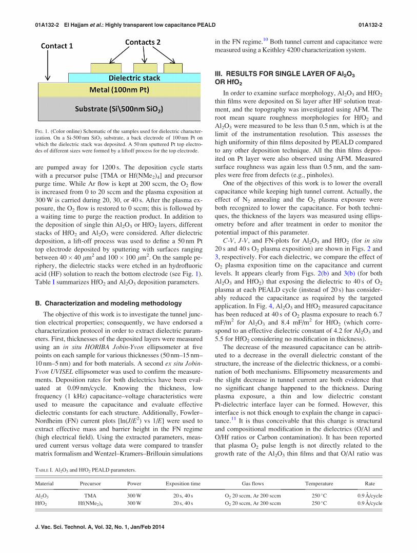
acid (HF) solution to reach the bottom electrode (see Fig. 1).
Table I summarizes HfO2 and Al2O3 deposition parameters.
B. Characterization and modeling methodology
The objective of this work is to investigate the tunnel junc-
tion electrical properties; consequently, we have endorsed a
characterization protocol in order to extract dielectric param-
eters. First, thicknesses of the deposited layers were measured
using an in situ HORIBA Jobin-Yvon ellipsometer at five
points on each sample for various thicknesses (50 nm–15 nm–
10 nm–5 nm) and for both materials. A second ex situ Jobin-Yvon UVISEL ellipsometer was used to confirm the measure-
ments. Deposition rates for both dielectrics have been eval-
uated at 0.09 nm/cycle. Knowing the thickness, low
frequency (1 kHz) capacitance–voltage characteristics were
used to measure the capacitance and evaluate effective
dielectric constants for each structure. Additionally, Fowler–
Nordheim (FN) current plots [ln(J/E2) vs 1/E] were used to
extract effective mass and barrier height in the FN regime
(high electrical field). Using the extracted parameters, meas-
ured current versus voltage data were compared to transfer
matrix formalism and Wentzel–Kramers–Brillouin simulations
in the FN regime.10 Both tunnel current and capacitance were
measured using a Keithley 4200 characterization system.
III. RESULTS FOR SINGLE LAYER OF Al2O3
OR HfO2
In order to examine surface morphology, Al2O3 and HfO2
thin films were deposited on Si layer after HF solution treat-
ment, and the topography was investigated using AFM. The
root mean square roughness morphologies for HfO2 and
Al2O3 were measured to be less than 0.5 nm, which is at the
limit of the instrumentation resolution. This assesses the
high uniformity of thin films deposited by PEALD compared
to any other deposition technique. All the thin films depos-
ited on Pt layer were also observed using AFM. Measured
surface roughness was again less than 0.5 nm, and the sam-
ples were free from defects (e.g., pinholes).
One of the objectives of this work is to lower the overall
capacitance while keeping high tunnel current. Actually, the
effect of N2 annealing and the O2 plasma exposure were
both recognized to lower the capacitance. For both techni-
ques, the thickness of the layers was measured using ellips-
ometry before and after treatment in order to monitor the
potential impact of this parameter.
C-V, J-V, and FN-plots for Al2O3 and HfO2 (for in situ20 s and 40 s O2 plasma exposition) are shown in Figs. 2 and
3, respectively. For each dielectric, we compare the effect of
O2 plasma exposition time on the capacitance and current
levels. It appears clearly from Figs. 2(b) and 3(b) (for both
Al2O3 and HfO2) that exposing the dielectric to 40 s of O2
plasma at each PEALD cycle (instead of 20 s) has consider-
ably reduced the capacitance as required by the targeted
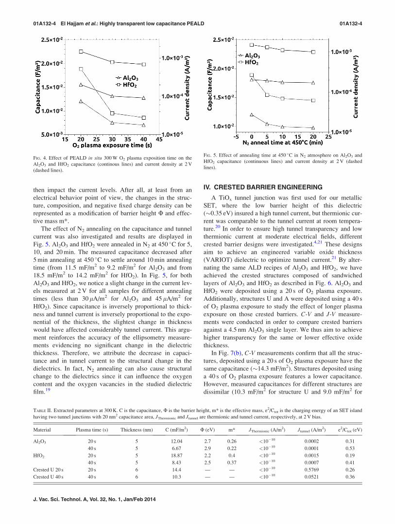
application. In Fig. 4, Al2O3 and HfO2 measured capacitance
has been reduced at 40 s of O2 plasma exposure to reach 6.7
mF/m2 for Al2O3 and 8.4 mF/m2 for HfO2 (which corre-
spond to an effective dielectric constant of 4.2 for Al2O3 and
5.5 for HfO2 considering no modification in thickness).
The decrease of the measured capacitance can be attrib-
uted to a decrease in the overall dielectric constant of the
structure, the increase of the dielectric thickness, or a combi-
nation of both mechanisms. Ellipsometry measurements and
the slight decrease in tunnel current are both evidence that
no significant change happened to the thickness. During
plasma exposure, a thin and low dielectric constant
Pt-dielectric interface layer can be formed. However, this
interface is not thick enough to explain the change in capaci-
tance.11 It is thus conceivable that this change is structural
and compositional modification in the dielectrics (O/Al and
O/Hf ratios or Carbon contamination). It has been reported
that plasma O2 pulse length is not directly related to the
growth rate of the Al2O3 thin films and that O/Al ratio was
FIG. 1. (Color online) Schematic of the samples used for dielectric character-
ization. On a Si-500 nm SiO2 substrate, a back electrode of 100 nm Pt on
which the dielectric stack was deposited. A 50 nm sputtered Pt top electro-
des of different sizes were formed by a liftoff process for the top electrode.
TABLE I. Al2O3 and HfO2 PEALD parameters.
Material Precursor Power Exposition time Gas flows Temperature Rate
Al2O3 TMA 300 W 20 s, 40 s O2 20 sccm, Ar 200 sccm 250 �C 0.9 A/cycle
HfO2 Hf(NMe2)4 300 W 20 s, 40 s O2 20 sccm, Ar 200 sccm 250 �C 0.9 A/cycle
01A132-2 El Hajjam et al.: Highly transparent low capacitance PEALD 01A132-2
J. Vac. Sci. Technol. A, Vol. 32, No. 1, Jan/Feb 2014
reduced with increasing pulse length.12 This means that in
addition to the removal of -CH3 group by oxygen radicals,
which happens during the first 20 s of exposure, the extended
exposure may have formed a denser and amorphous Al-O-Al
network, which is in agreement with the O/Al ratio.13
Currents for Al2O3 and HfO2 films were plotted versus
applied voltage in Figs. 2(a) and 3(a). From FN plots in Figs.
2(c) and 3(c), slopes were calculated at high electric field for
the four studied dielectrics. Those slopes were used to
extract barrier height U and effective mass m*, which were
then verified against J-V characteristics at high electric field
[in Figs. 2(a) and 3(a)]. The extracted parameters are
described in Table II. It can be noticed that tunnel current
was reduced (about 1 decade), which is marked by a shift to
the right in positive voltage in Figs. 2(a) and 3(a). As addi-
tional negative charges within the dielectric would increase
the potential barrier, this shift can be attributed to the
increase in negative fixed charges.14 It is known that Al2O3
and HfO2 films can have important negative fixed charges
density.15,16 Negative fixed charges can be partially
explained by the impact of vacuum ultraviolet radiation
from the plasma. In fact, negative charge density is propor-
tional to the plasma exposure time.17,18 In Figs. 2(a) and
3(a), the third fit shows that the addition of negative charge
density (0.0015 C/m2 for Al2O3 and 0.0021 C/m2 for HfO2)
to the studied films can explain the decrease in tunnel cur-
rent. However, decrease in permittivity suggests change in
the structure and composition of the material, which can
FIG. 2. (Color online) Effect of 20 s and 40 s exposure of Al2O3 to O2 plasma
on electrical properties; (a) J-V, (b) C-V, and (c) FN-plot (measurement at
300 K).
FIG. 3. (Color online) Effect of 20 s and 40 s exposure of HfO2 to O2 plasma
on electrical properties; (a) J-V, (b) C-V, and (c) FN-plot (measurement at
300 K).
01A132-3 El Hajjam et al.: Highly transparent low capacitance PEALD 01A132-3
JVST A - Vacuum, Surfaces, and Films
then impact the current levels. After all, at least from an
electrical behavior point of view, the changes in the struc-
ture, composition, and negative fixed charge density can be
represented as a modification of barrier height U and effec-
tive mass m*.
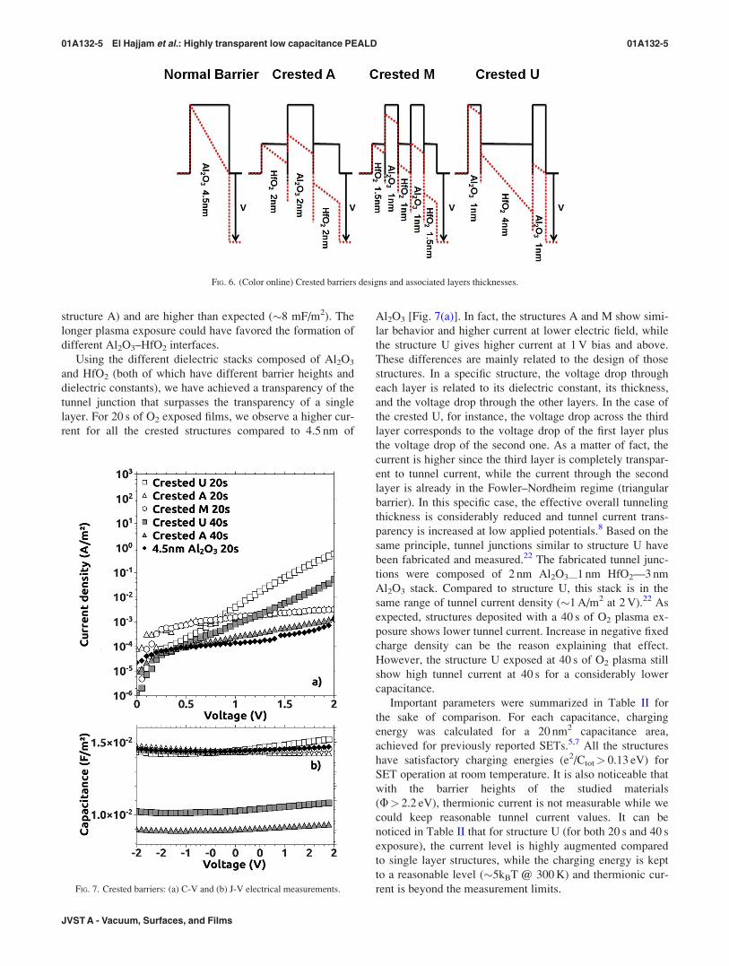
The effect of N2 annealing on the capacitance and tunnel
current was also investigated and results are displayed in
Fig. 5. Al2O3 and HfO2 were annealed in N2 at 450 �C for 5,
10, and 20 min. The measured capacitance decreased after
5 min annealing at 450 �C to settle around 10 min annealing
time (from 11.5 mF/m2 to 9.2 mF/m2 for Al2O3 and from
18.5 mF/m2 to 14.2 mF/m2 for HfO2). In Fig. 5, for both
Al2O3 and HfO2, we notice a slight change in the current lev-
els measured at 2 V for all samples for different annealing
times (less than 30 lA/m2 for Al2O3 and 45 lA/m2 for
HfO2). Since capacitance is inversely proportional to thick-
ness and tunnel current is inversely proportional to the expo-
nential of the thickness, the slightest change in thickness
would have affected considerably tunnel current. This argu-
ment reinforces the accuracy of the ellipsometry measure-
ments evidencing no significant change in the dielectric
thickness. Therefore, we attribute the decrease in capaci-
tance and in tunnel current to the structural change in the
dielectrics. In fact, N2 annealing can also cause structural
change to the dielectrics since it can influence the oxygen
content and the oxygen vacancies in the studied dielectric
film.19
IV. CRESTED BARRIER ENGINEERING
A TiOx tunnel junction was first used for our metallic
SET, where the low barrier height of this dielectric
(�0.35 eV) insured a high tunnel current, but thermionic cur-
rent was comparable to the tunnel current at room tempera-
ture.20 In order to ensure high tunnel transparency and low
thermionic current at moderate electrical fields, different
crested barrier designs were investigated.4,21 These designs
aim to achieve an engineered variable oxide thickness
(VARIOT) dielectric to optimize tunnel current.21 By alter-
nating the same ALD recipes of Al2O3 and HfO2, we have
achieved the crested structures composed of sandwiched
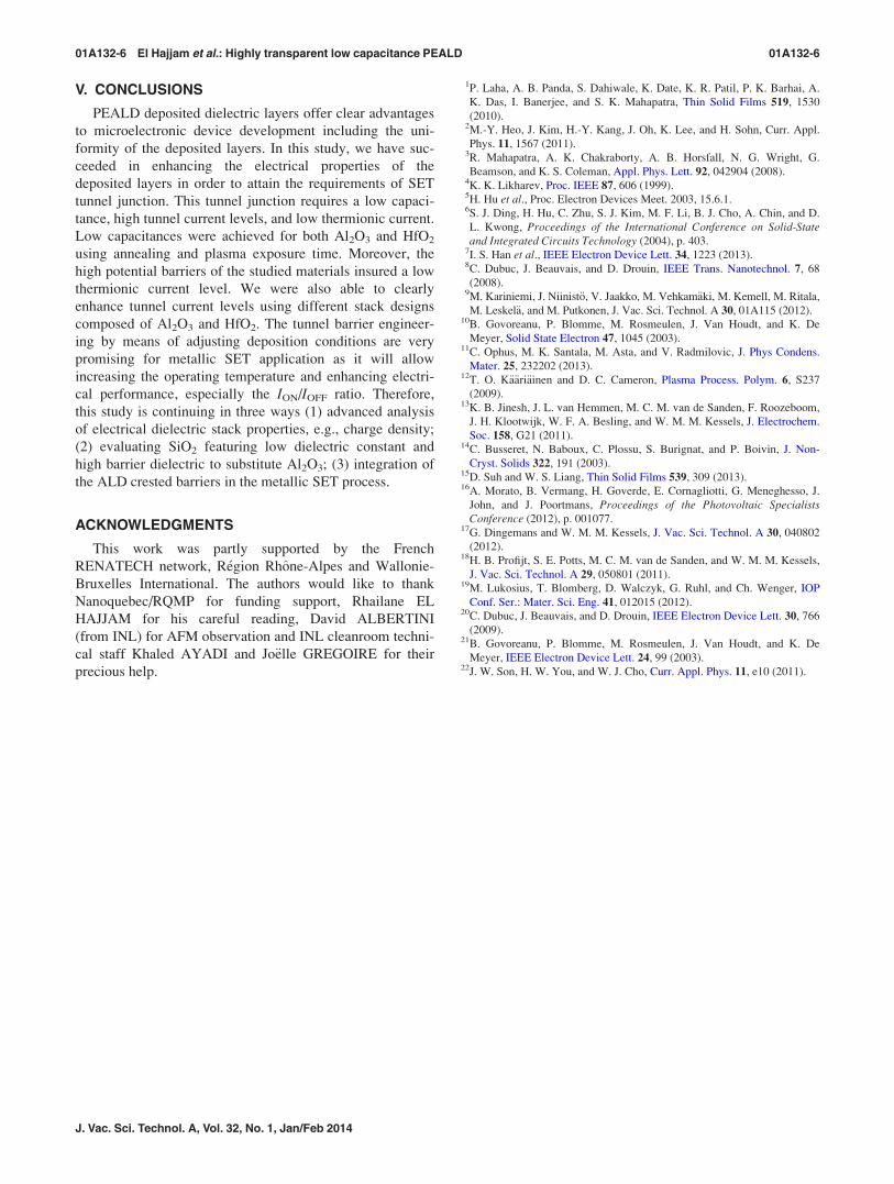
layers of Al2O3 and HfO2 as described in Fig. 6. Al2O3 and
HfO2 were deposited using a 20 s of O2 plasma exposure.
Additionally, structures U and A were deposited using a 40 s
of O2 plasma exposure to study the effect of longer plasma
exposure on those crested barriers. C-V and J-V measure-
ments were conducted in order to compare crested barriers
against a 4.5 nm Al2O3 single layer. We thus aim to achieve
higher transparency for the same or lower effective oxide
thickness.
In Fig. 7(b), C-V measurements confirm that all the struc-
tures, deposited using a 20 s of O2 plasma exposure have the
same capacitance (�14.3 mF/m2). Structures deposited using
a 40 s of O2 plasma exposure features a lower capacitance.
However, measured capacitances for different structures are
dissimilar (10.3 mF/m2 for structure U and 9.0 mF/m2 for
FIG. 4. Effect of PEALD in situ 300 W O2 plasma exposition time on the
Al2O3 and HfO2 capacitance (continous lines) and current density at 2 V
(dashed lines).
TABLE II. Extracted parameters at 300 K. C is the capacitance, U is the barrier height, m* is the effective mass, e2/Ctot is the charging energy of an SET island
having two tunnel junctions with 20 nm2 capacitance area, JThermionic and Jtunnel are thermionic and tunnel current, respectively, at 2 V bias.
Material Plasma time (s) Thickness (nm) C (mF/m2) U (eV) m* JThermionic (A/m2) Jtunnel (A/m2) e2/Ctot (eV)
Al2O3 20 s 5 12.04 2.7 0.26 <10�10 0.0002 0.31
40 s 5 6.67 2.9 0.22 <10�10 0.0001 0.53
HfO2 20 s 5 18.87 2.2 0.4 <10�10 0.0015 0.19
40 s 5 8.43 2.5 0.37 <10�10 0.0007 0.41
Crested U 20 s 20 s 6 14.4 — — <10�10 0.5769 0.26
Crested U 40 s 40 s 6 10.3 — — <10�10 0.0521 0.36
FIG. 5. Effect of annealing time at 450 �C in N2 atmosphere on Al2O3 and
HfO2 capacitance (continuous lines) and current density at 2 V (dashed
lines).
01A132-4 El Hajjam et al.: Highly transparent low capacitance PEALD 01A132-4
J. Vac. Sci. Technol. A, Vol. 32, No. 1, Jan/Feb 2014
structure A) and are higher than expected (�8 mF/m2). The
longer plasma exposure could have favored the formation of
different Al2O3–HfO2 interfaces.
Using the different dielectric stacks composed of Al2O3
and HfO2 (both of which have different barrier heights and
dielectric constants), we have achieved a transparency of the
tunnel junction that surpasses the transparency of a single
layer. For 20 s of O2 exposed films, we observe a higher cur-
rent for all the crested structures compared to 4.5 nm of
Al2O3 [Fig. 7(a)]. In fact, the structures A and M show simi-
lar behavior and higher current at lower electric field, while
the structure U gives higher current at 1 V bias and above.
These differences are mainly related to the design of those
structures. In a specific structure, the voltage drop through
each layer is related to its dielectric constant, its thickness,
and the voltage drop through the other layers. In the case of
the crested U, for instance, the voltage drop across the third
layer corresponds to the voltage drop of the first layer plus
the voltage drop of the second one. As a matter of fact, the
current is higher since the third layer is completely transpar-
ent to tunnel current, while the current through the second
layer is already in the Fowler–Nordheim regime (triangular
barrier). In this specific case, the effective overall tunneling
thickness is considerably reduced and tunnel current trans-
parency is increased at low applied potentials.8 Based on the
same principle, tunnel junctions similar to structure U have
been fabricated and measured.22 The fabricated tunnel junc-
tions were composed of 2 nm Al2O3—1 nm HfO2—3 nm
Al2O3 stack. Compared to structure U, this stack is in the
same range of tunnel current density (�1 A/m2 at 2 V).22 As
expected, structures deposited with a 40 s of O2 plasma ex-
posure shows lower tunnel current. Increase in negative fixed
charge density can be the reason explaining that effect.
However, the structure U exposed at 40 s of O2 plasma still
show high tunnel current at 40 s for a considerably lower
capacitance.
Important parameters were summarized in Table II for
the sake of comparison. For each capacitance, charging
energy was calculated for a 20 nm2 capacitance area,
achieved for previously reported SETs.5,7 All the structures
have satisfactory charging energies (e2/Ctot> 0.13 eV) for
SET operation at room temperature. It is also noticeable that
with the barrier heights of the studied materials
(U> 2.2 eV), thermionic current is not measurable while we
could keep reasonable tunnel current values. It can be
noticed in Table II that for structure U (for both 20 s and 40 s
exposure), the current level is highly augmented compared
to single layer structures, while the charging energy is kept
to a reasonable level (�5kBT @ 300 K) and thermionic cur-
rent is beyond the measurement limits.
FIG. 6. (Color online) Crested barriers designs and associated layers thicknesses.
FIG. 7. Crested barriers: (a) C-V and (b) J-V electrical measurements.
01A132-5 El Hajjam et al.: Highly transparent low capacitance PEALD 01A132-5
JVST A - Vacuum, Surfaces, and Films
V. CONCLUSIONS
PEALD deposited dielectric layers offer clear advantages
to microelectronic device development including the uni-
formity of the deposited layers. In this study, we have suc-
ceeded in enhancing the electrical properties of the
deposited layers in order to attain the requirements of SET
tunnel junction. This tunnel junction requires a low capaci-
tance, high tunnel current levels, and low thermionic current.
Low capacitances were achieved for both Al2O3 and HfO2
using annealing and plasma exposure time. Moreover, the
high potential barriers of the studied materials insured a low
thermionic current level. We were also able to clearly
enhance tunnel current levels using different stack designs
composed of Al2O3 and HfO2. The tunnel barrier engineer-
ing by means of adjusting deposition conditions are very
promising for metallic SET application as it will allow
increasing the operating temperature and enhancing electri-
cal performance, especially the ION/IOFF ratio. Therefore,
this study is continuing in three ways (1) advanced analysis
of electrical dielectric stack properties, e.g., charge density;
(2) evaluating SiO2 featuring low dielectric constant and
high barrier dielectric to substitute Al2O3; (3) integration of
the ALD crested barriers in the metallic SET process.
ACKNOWLEDGMENTS
This work was partly supported by the French
RENATECH network, R�egion Rhone-Alpes and Wallonie-
Bruxelles International. The authors would like to thank
Nanoquebec/RQMP for funding support, Rhailane EL
HAJJAM for his careful reading, David ALBERTINI
(from INL) for AFM observation and INL cleanroom techni-
cal staff Khaled AYADI and Jo€elle GREGOIRE for their
precious help.
1P. Laha, A. B. Panda, S. Dahiwale, K. Date, K. R. Patil, P. K. Barhai, A.
K. Das, I. Banerjee, and S. K. Mahapatra, Thin Solid Films 519, 1530
(2010).2M.-Y. Heo, J. Kim, H.-Y. Kang, J. Oh, K. Lee, and H. Sohn, Curr. Appl.
Phys. 11, 1567 (2011).3R. Mahapatra, A. K. Chakraborty, A. B. Horsfall, N. G. Wright, G.
Beamson, and K. S. Coleman, Appl. Phys. Lett. 92, 042904 (2008).4K. K. Likharev, Proc. IEEE 87, 606 (1999).5H. Hu et al., Proc. Electron Devices Meet. 2003, 15.6.1.6S. J. Ding, H. Hu, C. Zhu, S. J. Kim, M. F. Li, B. J. Cho, A. Chin, and D.
L. Kwong, Proceedings of the International Conference on Solid-Stateand Integrated Circuits Technology (2004), p. 403.
7I. S. Han et al., IEEE Electron Device Lett. 34, 1223 (2013).8C. Dubuc, J. Beauvais, and D. Drouin, IEEE Trans. Nanotechnol. 7, 68
(2008).9M. Kariniemi, J. Niinist€o, V. Jaakko, M. Vehkam€aki, M. Kemell, M. Ritala,
M. Leskel€a, and M. Putkonen, J. Vac. Sci. Technol. A 30, 01A115 (2012).10B. Govoreanu, P. Blomme, M. Rosmeulen, J. Van Houdt, and K. De
Meyer, Solid State Electron 47, 1045 (2003).11C. Ophus, M. K. Santala, M. Asta, and V. Radmilovic, J. Phys Condens.
Mater. 25, 232202 (2013).12T. O. K€a€ari€ainen and D. C. Cameron, Plasma Process. Polym. 6, S237
(2009).13K. B. Jinesh, J. L. van Hemmen, M. C. M. van de Sanden, F. Roozeboom,
J. H. Klootwijk, W. F. A. Besling, and W. M. M. Kessels, J. Electrochem.
Soc. 158, G21 (2011).14C. Busseret, N. Baboux, C. Plossu, S. Burignat, and P. Boivin, J. Non-
Cryst. Solids 322, 191 (2003).15D. Suh and W. S. Liang, Thin Solid Films 539, 309 (2013).16A. Morato, B. Vermang, H. Goverde, E. Cornagliotti, G. Meneghesso, J.
John, and J. Poortmans, Proceedings of the Photovoltaic SpecialistsConference (2012), p. 001077.
17G. Dingemans and W. M. M. Kessels, J. Vac. Sci. Technol. A 30, 040802
(2012).18H. B. Profijt, S. E. Potts, M. C. M. van de Sanden, and W. M. M. Kessels,
J. Vac. Sci. Technol. A 29, 050801 (2011).19M. Lukosius, T. Blomberg, D. Walczyk, G. Ruhl, and Ch. Wenger, IOP
Conf. Ser.: Mater. Sci. Eng. 41, 012015 (2012).20C. Dubuc, J. Beauvais, and D. Drouin, IEEE Electron Device Lett. 30, 766
(2009).21B. Govoreanu, P. Blomme, M. Rosmeulen, J. Van Houdt, and K. De
Meyer, IEEE Electron Device Lett. 24, 99 (2003).22J. W. Son, H. W. You, and W. J. Cho, Curr. Appl. Phys. 11, e10 (2011).
01A132-6 El Hajjam et al.: Highly transparent low capacitance PEALD 01A132-6
J. Vac. Sci. Technol. A, Vol. 32, No. 1, Jan/Feb 2014


![Présentation1 [Enregistré automatiquement]...album en (Francis Saucisson contre rage bête de Nicolas Pinet), Biscoto devient parallèlement au journal une maison dédition qui éditera](https://img.pdfslide.fr/doc/110x75/5f68b6fedb8b9f27e508482e/prsentation1-enregistr-automatiquement-album-en-francis-saucisson-contre.jpg)