Embed Size (px)
Citation preview
Lien optique transcutané pour l’enregistrement designaux neuronaux haute résolution
Mémoire
Mouhamad Al Yassine
Maitrise en Génie ÉlectriqueMaître ès sciences (M.Sc.)
Québec, Canada
© Mouhamad Al Yassine, 2015

Résumé
L’enregistrement des données de neurones a connu d’énormes progrès au cours des dernières années ;
il aide à diagnostiquer les maladies à l’intérieur du cerveau comme la maladie de Parkinson et la
dépression clinique. Un grand nombre de patients atteints de Parkinson utilisent un implant neuronal
pour réduire les tumeurs et le mouvement rigide. Afin de contrôler le mouvement, une petite électrode
est placée sur le cerveau pour réduire et même éliminer les symptômes de Parkinson au moment où
une simulation électrique arrive.
Le système d’enregistrement de données de neurones exige un lien complet. En utilisant des micro-
électrodes, on prend les données provenant des neurones dans le cerveau, on les convertis en données
numériques et ensuite on transmet ces données numérisées en utilisant une liaison sans fil. Dans ce
travail, nous nous concentrons sur l’envoi de données de neurones à partir d’un dispositif implanté à
travers la peau en utilisant la lumière. Il y’a différentes façons de transmettre les données sans fil, soit
avec antenne, soit avec un émetteur optique ; nous discutons à propos de ces méthodes dans le chapitre
de la revue de la littérature. Nous avons choisi de travailler avec Émettant VCSEL ou Vertical Cavity
Surface lasers ; une diode laser spécialisée avec une meilleure efficacité et une vitesse élevée par rap-
port à d’autres dispositifs optiques. La première partie de la recherche était d’étudier la meilleure
façon de transmettre des données à travers la peau humaine, le mode de transmission et les propriétés
du milieu à travers lequel la lumière se propage. Après avoir choisi le mode de transmission, nous
avons conçu un lien intégré en utilisant la technologie de 0,18 um CMOS. Ce lien intégré est constitué
de deux parties, du côté de l’émetteur, qui est un moteur apte à entraîner le VCSEL avec un dB bande
passante à 3 de 1,3 GHz et une faible consommation de puissance de 12 mW, et un côté récepteur qui
se compose d’une photodiode reliée à un VCSEL CMOS amplificateur d’adaptation d’impédance à
gain élevé (90 dB) et haute vitesse de (250 Mbps).
La deuxième partie était de construire une liaison optique discrète avec des composants à faible coût
commercial, donc nous avons conçu deux PCB (Printed Circuit Board) pour le côté émetteur ainsi que
le côté récepteur, et nous avons conçu un système mécanique pour aligner l’émetteur et la photodiode.
Nous avons ensuite testé notre liaison optique, ce qui a démontré la capacité de transmettre des don-
nées par le biais de 3 mm de tissu de porc à un débit binaire de 20 Mbps avec une faible consommation
d’énergie de 3 MW en utilisant OOK (On Off Keying) la transmission de données, et enfin nous avons
fait une comparaison entre nos résultats et d’autres œuvres.
iii

Abstract
Neural data recording has seen huge progress during the past few years; it helps for diagnosing dis-
eases inside the brain like Parkinson disease and clinical depression. A big number of Parkinson’s
patients use a neural implant to lessen tumors and rigid movement. A small electrode will be placed
on the brain. It helps to control motion and when an electrical simulation happens, it helps reduce
and even eliminate Parkinson symptoms. The neural data recording system requires a complete link
starting by recording neural data using electrodes, convert this data onto digital data and transmit the
digitized data using a wireless link. In this work we are focusing on sending neural data from an im-
planted device through the skin using light. There are different ways to transmit data wirelessly with
either antenna or with an optical transmitter; we discuss about those methods in the literature review
chapter. We choose to work with VCSEL or Vertical Cavity Surface Emitting Lasers; a specialized
laser diode with improved efficiency and high speed compared to other optical devices.
The first part of the research was to study the best way to transmit data through the human skin, the
method of transmission and the properties of the medium through which the light will propagate.
After choosing the method of transmission, we designed an integrated link using 0.18 um CMOS
technology. This integrated link consists of two parts, the transmitter side which is a VCSEL driver
able to drive the VCSEL with a 3 dB bandwidth of 1.3 GHz and low power-consumption of 12 mW,
and a receiver side that consists of a photodiode connected to a CMOS transimpedance amplifier with
high gain (90 dB) and high speed of (250 Mbps).
The second part was to build a discrete optical link with commercial low cost components, so we
designed two PCBs (Printed Circuit Board) for the transmitter and receiver side, and we designed a
mechanical system to align the transmitter and the photodiode. We then tested our optical link, and it
demonstrated the capability to transmit data through 3 mm of pork tissue at a bit-rate of 20 Mbps with
low power consumption of 3 mW using OOK (On Off Keying) data transmission, and finally we did
a comparison between our results and other works.
v

Table des matières
Résumé iii
Abstract v
Table des matières vii
Liste des tableaux ix
Liste des figures xi
Abréviations xiii
Remerciements xv
Introduction 1
1 Literature Review 31.1 Introduction . . . . . . . . . . . . . . . . . . . . . . . . . . . . . . . . . . . . . 31.2 Transcutaneous link . . . . . . . . . . . . . . . . . . . . . . . . . . . . . . . . . 41.3 Transimpedance Amplifier . . . . . . . . . . . . . . . . . . . . . . . . . . . . . 61.4 Data modulation . . . . . . . . . . . . . . . . . . . . . . . . . . . . . . . . . . . 7
2 Transcutaneous optical link design methodology 132.1 Design specifications . . . . . . . . . . . . . . . . . . . . . . . . . . . . . . . . 132.2 Method of data transmission . . . . . . . . . . . . . . . . . . . . . . . . . . . . 142.3 Essentials of optical communication . . . . . . . . . . . . . . . . . . . . . . . . 142.4 Skin’s Optical properties . . . . . . . . . . . . . . . . . . . . . . . . . . . . . . 162.5 Safety hazards . . . . . . . . . . . . . . . . . . . . . . . . . . . . . . . . . . . . 192.6 Conclusion . . . . . . . . . . . . . . . . . . . . . . . . . . . . . . . . . . . . . 20
3 Integrated Link Design Using 0.18 um CMOS Technology 213.1 CMOS Transimpedance Amplifier . . . . . . . . . . . . . . . . . . . . . . . . . 213.2 VCSEL driver . . . . . . . . . . . . . . . . . . . . . . . . . . . . . . . . . . . . 253.3 Conclusion . . . . . . . . . . . . . . . . . . . . . . . . . . . . . . . . . . . . . 30
4 Discrete Link Design 334.1 Introduction . . . . . . . . . . . . . . . . . . . . . . . . . . . . . . . . . . . . . 334.2 Link Design . . . . . . . . . . . . . . . . . . . . . . . . . . . . . . . . . . . . . 334.3 Experimental setup . . . . . . . . . . . . . . . . . . . . . . . . . . . . . . . . . 36
vii

4.4 Experimental Results . . . . . . . . . . . . . . . . . . . . . . . . . . . . . . . . 374.5 Comparison . . . . . . . . . . . . . . . . . . . . . . . . . . . . . . . . . . . . . 39
Conclusion 41
A In Air Optical Link 43
Bibliographie 45
viii
Liste des tableaux
3.1 Transistors Aspect Ratio (W/L) . . . . . . . . . . . . . . . . . . . . . . . . . . . . . 233.2 components values used in the simulation . . . . . . . . . . . . . . . . . . . . . . . 243.3 Transistors Aspect Ratio (W/L) . . . . . . . . . . . . . . . . . . . . . . . . . . . . . 273.4 components values used in the simulation. . . . . . . . . . . . . . . . . . . . . . . . 283.5 TIA performance summary . . . . . . . . . . . . . . . . . . . . . . . . . . . . . . . 313.6 VCSEL driver performance summary. . . . . . . . . . . . . . . . . . . . . . . . . . 31
4.1 components values used in the circuit. . . . . . . . . . . . . . . . . . . . . . . . . . 364.2 Comparison between different optical transmitters. . . . . . . . . . . . . . . . . . . 394.3 Summary of the some TOLs using different Optical transmitter. . . . . . . . . . . . . 40
ix

Liste des figures
0.1 Patient receiving treatment at Braingate laboratory reprinted from [1]. . . . . . . . . 2
1.1 TIA schematic. . . . . . . . . . . . . . . . . . . . . . . . . . . . . . . . . . . . . . 71.2 Transmission power comparison reprinted from[2]. . . . . . . . . . . . . . . . . . . 91.3 Bandwidth required comparison reprinted from [2]. . . . . . . . . . . . . . . . . . . 101.4 Transmission capacity comparison reprinted from[2]. . . . . . . . . . . . . . . . . . 11
2.1 Section through human skin and underlying structures [3]. . . . . . . . . . . . . . . 172.2 chromophores absorption coefficient with respect to wavelenghts [4]. . . . . . . . . . 172.3 The absorption coefficients for human skin reprinted from [5]. . . . . . . . . . . . . 182.4 The scattering coefficients for human skin reprinted from [5]. . . . . . . . . . . . . . 19
3.1 current-mode TIA topology[6] . . . . . . . . . . . . . . . . . . . . . . . . . . . . . 223.2 Schematic of three-stage current-mode TIA . . . . . . . . . . . . . . . . . . . . . . . 223.3 AC performance of the current-mode TIA. . . . . . . . . . . . . . . . . . . . . . . . 253.4 input referred noise of the TIA. . . . . . . . . . . . . . . . . . . . . . . . . . . . . . 253.5 The input current pulse and the output voltage at the 3rd stage for a 10 nF capacitive
load. . . . . . . . . . . . . . . . . . . . . . . . . . . . . . . . . . . . . . . . . . . . 263.6 inverter output for a 10 nF capacitive load. . . . . . . . . . . . . . . . . . . . . . . . 263.7 The VCSEL driver schematic. . . . . . . . . . . . . . . . . . . . . . . . . . . . . . 283.8 The 3−dBBandwidth of the VCSEL driver for a 10 nF capacitive load. . . . . . . . 293.9 The output pulse at the input of the VCSEL. . . . . . . . . . . . . . . . . . . . . . . 293.10 The output current versus the input bias voltage. . . . . . . . . . . . . . . . . . . . . 30
4.1 NPN VCSEL driver circuit. . . . . . . . . . . . . . . . . . . . . . . . . . . . . . . . 354.2 PCB layout for the Transmitter side. . . . . . . . . . . . . . . . . . . . . . . . . . . 354.3 Receiver side schematic. . . . . . . . . . . . . . . . . . . . . . . . . . . . . . . . . 364.4 PCB layout for the receiver side. . . . . . . . . . . . . . . . . . . . . . . . . . . . . 364.5 The builded symstem to align The VCSEL and the Photodiode. . . . . . . . . . . . . 374.6 Three holes of 1mm separating distance to get 1, 2mm of misalignment. . . . . . . . 38
A.1 conceptual representation of the Optical link inside the cage . . . . . . . . . . . . . 43
xi


Abréviations
TOL Transcutaneous Optical Link
VCSEL Vertical Cavity Surface Emitting Laser
LED Light Emitting Diode
BER Bit Error Rate
ANSI American National Standards Institute
UWB Ultra Wide Band
RF Radio Frequency
MICS Medical Implant Communication Service
OOK ON OFF Keying
TIA Transimpedance Amplifier
Rd photodiode dark resistance, typically greater than 100 MΩ
Cd photodiode junction capacitance
PPM pulse position modulation
DPIM Digital Pulse Interval Modulation
Rb Bit Rate
IR Infra-Red
NRZ Non Return to Zero
RZ Return to Zero
BW Bandwidth
SNR Signal to Noise Ratio
FSK Frequency Shift Keying
IRN Input Referred Noise
xiii

Remerciements
Foremost, i would like to express my sincere gratitude to my advisor Prof. Benoit Gosselin for his
continuous support and guidance in those 2 years, it has been a great pleasure to work with you. You
have a set an example of exellence as a researcher, instructor and role model.
I would like to thank my Co-Director Prof.Younes Messadeq for his kindness and his comprehension
and for his endless support. I could not have imagined having a better co-director and mentor for my
master study.
I would like to thank my thesis comitte members.
I would like to thank my colleagues Abdullah Mirbozorgi, Masoud, Ali Reza and many other. You
really showed a great support and you helped me a lot.
I would specialy like to thank my familly and my friends for always being next to me and encouraging
me through the 2 years. In particular i would like to thank my mom Yemen El-Mourad and my dad
Omar Al Yassine for being the most supportive, loving and driven people I have ever known. They
truly push me beyond all of the boundaries I thought I’ve never be able to reach. I would like also to
thank my uncle Prof. Walid EL-Mourad for his no limited guidance and help, i undoubtedly could not
have done this without you.
xv

Introduction
Prosthetic, referring to the prosthesis is an artificial replacement for a missing part in the body as a
tooth, leg or an arm, etc. A prosthetic device is designed generally even for a cosmetic reason involving
a treatment intended to restore or improve person’s appearance or in the main goal for a functional
reason to restore the ability of a patient who has loss a part of his body. This prosthetic device can be
permanently implanted like a tooth, an artificial hip or a cardiac prosthetic, etc., or it can be removable,
which is the case for most prosthetic arms and legs is.
The evolution of prosthetics is a long history from its beginnings to nowadays where during this
evolution period, we saw a lot of progress that increases the quality of life for patients. Till nowadays
and this field is still under progress, a lot of problems were solved with those prosthetic devices, the
improvement is shown now with adding small implanted chips and micro-controller to the devices
to let the patient return to his old lifestyle, he used to live rather than simply provide to him basic
functionality.
In the past years, there has been great progress in implantable medical devices. A lot of diseases and
disabilities can be treated by implanting an electronic chip inside the human body ; these implanted
devices have greatly improved the life of patients. For example, now, we can replace the amputated
arm with a prosthetic and provide the patient the ability to move his prosthetic arm the way he wants
simply by adding some microelectrode on the neural centre of the brain to receive the order that the
brain sends and programs the prosthetic arm to move simply under this order. Braingate group is a
research team which includes neurologists, neuroscientists, engineers and other researchers from dif-
ferent universities as Brown University, Cas western Reserve university and Stanford university in
collaboration with Massachusetts General Hospitala in America. All focused on developing technolo-
gies to sense, transmit, analyze, and apply the language of neurons. As shown in Fig 0.1 a photo of
a patient receiving treatment at Braingate laboratory, Recently they improved and developed several
options for people with disabilities, so they can, for example, control a robotic arm or control their
television and computer.
As for neural recording system, it helps for diagnosing brain diseases and gives a way to overcome
these diseases. Neural recording Systems require simultaneous recording from a large number of
neurons and high speed communication between the implanted device and the external receiver. A
data rate from Mbps to tens Mbps is required, which brings a great challenge when realized with low
1
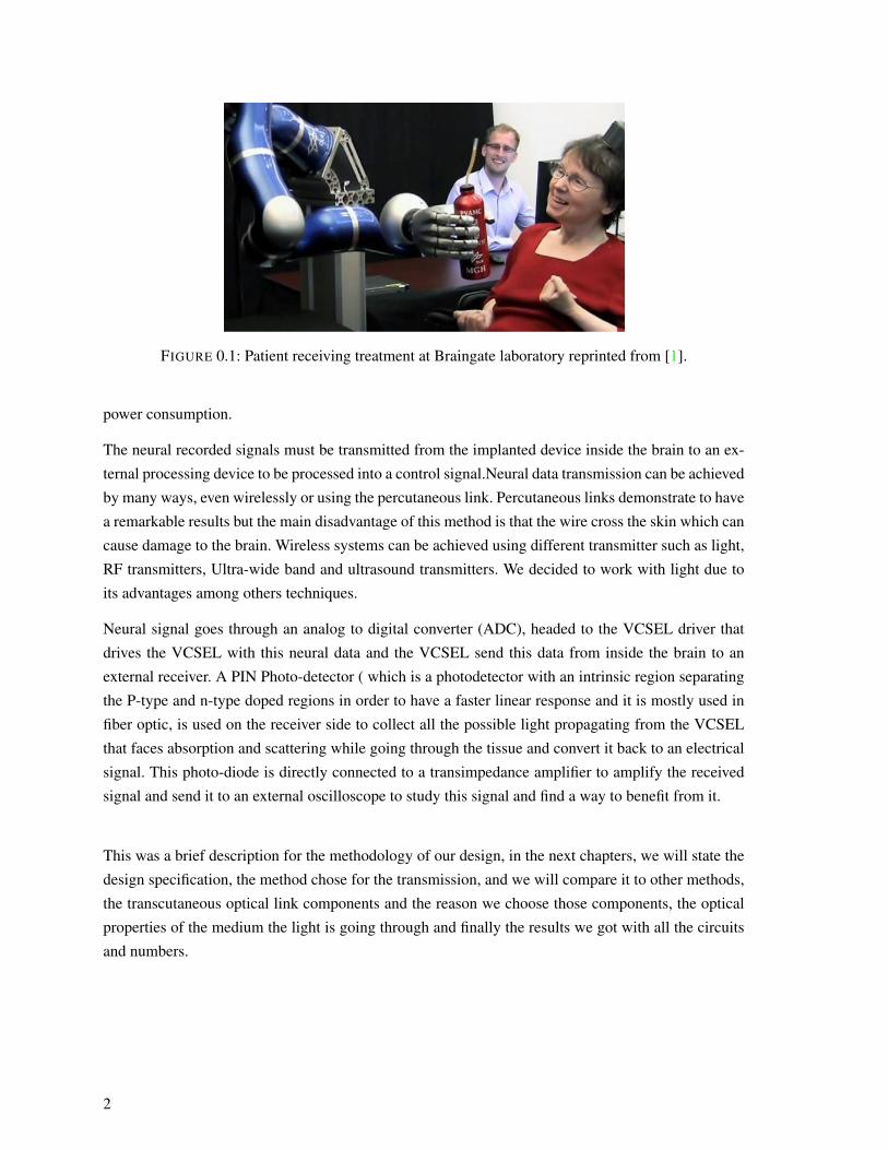
FIGURE 0.1: Patient receiving treatment at Braingate laboratory reprinted from [1].
power consumption.
The neural recorded signals must be transmitted from the implanted device inside the brain to an ex-
ternal processing device to be processed into a control signal.Neural data transmission can be achieved
by many ways, even wirelessly or using the percutaneous link. Percutaneous links demonstrate to have
a remarkable results but the main disadvantage of this method is that the wire cross the skin which can
cause damage to the brain. Wireless systems can be achieved using different transmitter such as light,
RF transmitters, Ultra-wide band and ultrasound transmitters. We decided to work with light due to
its advantages among others techniques.
Neural signal goes through an analog to digital converter (ADC), headed to the VCSEL driver that
drives the VCSEL with this neural data and the VCSEL send this data from inside the brain to an
external receiver. A PIN Photo-detector ( which is a photodetector with an intrinsic region separating
the P-type and n-type doped regions in order to have a faster linear response and it is mostly used in
fiber optic, is used on the receiver side to collect all the possible light propagating from the VCSEL
that faces absorption and scattering while going through the tissue and convert it back to an electrical
signal. This photo-diode is directly connected to a transimpedance amplifier to amplify the received
signal and send it to an external oscilloscope to study this signal and find a way to benefit from it.
This was a brief description for the methodology of our design, in the next chapters, we will state the
design specification, the method chose for the transmission, and we will compare it to other methods,
the transcutaneous optical link components and the reason we choose those components, the optical
properties of the medium the light is going through and finally the results we got with all the circuits
and numbers.
2
Chapitre 1
Literature Review
1.1 Introduction
Nowadays, sensory or motor modalities that are lost due to an injury or diseases [7] are to be replaced
by a group of medical devices that have a job to rescue and help the patient to recover the lost, for that
"Transcutaneous data link" plays an important role for the functioning of the implantable medical de-
vices [8]. Percutaneous Link has taken place at first as a link to deliver and receive data from and to the
implantable devices. It shows a great performance due to its high rate and accurate data transmitting,
but since it will cross the skin with a small wire then we are taking a risk to put the patient on danger
because that may cause an infection and brain damage. Visual prostheses and cochlear implants need
a big amount of data from the external devices to interface with the largest possible number of neurons
and produce clear sensation that can support the patient such as speech recognition[7]. In this case, the
information comes mainly from the external device to an implanted receiver inside the body, and this
is what it called forward telemetry. And the same implanted device has to inform the external device
about the neural response after the simulation to adjust if needed the simulation parameters[9][10].
This direction of data flow is called uplink. Another group of Neuroprosthetic devices, where the role
of the device is to record the largest possible amount of neural data using microelectrodes[11] and
sends it through the skin to the external components to be processed in order to know the patient
intentions[12][13]. Those processed data can be used to access several devices in order to drive them,
for example, we can drive a prosthetic arm with the neural data of the patient, so he can move the
arm in the way he wants to just by thinking about that, the brain will send an order to the prosthetic
arm that is programed to work with these neural data[14]. For the uplink and downlink dataflow there
are several common design challenges among both categories. Some of these challenges is the limited
space available for the device implantation, the power available inside the human body to feed the
implantable device. Other challenges like tissue absorption of a different kind of data transmission
wither electromagnetic waves or optical transmission, there will be some absorption and scattering for
the transmitted data.
3
1.2 Transcutaneous link
Although in the past few years, there has been a great progress in developing an optical link, starting
from increasing the speed of the link to decrease the power consumption and the bit error rate in order
to get a better link that serves our demands.
Neural data transmission can be achieved by many ways, even wirelessly or using the percutaneous
link. The percutaneous link demonstrates that this way can achieve remarkable results in BW and SNR
but the main problem of this method that it needs to pan the skin with some wires, which can damage
the brain and increase the possibility of infection, as we said before we are looking for a safety way
to send those neural data without putting any danger on the patient.
So we have to search for a method that can be done wirelessly without affecting the patient skin. Also
many methods have been released for such a goal like RF links, Ultra Wide Band (UWB), ultrasound
or infrared optical light ; all of them have some advantages and disadvantages. Ultrasonic acoustic link
can be used, and it offers high bandwidth, but it is not ideal for implanted devices because of the need
of high-voltage drivers.
Ming Yin [15] with his 100-channel fully implantable wireless broadband neural recording system
with an inductively rechargeable battery and RF data transfer has demonstrated that it is possible
to achieve high bit rate with RF transmission, a data telemetry that used 3.2 GHz to 3.8 GHz FSK
modulated wireless link to achieve a total rate of 48 Mbps Manchester encoded data with a 96 mW of
power consumption, external active cooling method were used to decrease the temperature produced
from the power consumption of the system to a safe level.
[16] mention that implantable microsystems cannot use batteries as a primary source and instead of
that we have to deliver the energy wirelessly across the skin using a inductive link formed by a pair of
coils, which is a safe method to power up our circuit. also it presents all the energy-efficient sensory
circuits to retrieve signals from neural probes and compare them.
Shahrokhi [17] reported a 128-channel integrated neural interface. It has a low-noise signal recording
and generation circuit for electrical neural activities’ monitoring and stimulation, respectively. It has
a 9.3 mW power consumption, and it use a wireless telemetry model for broadcasting the data to an
external receiving unit.
Moo sung Chae [18] reported on a 128-channel neural recording integrated circuit with a wireless
telemetry. This system was based on a UWB telemetry to wirelessly deliver the neural data from
128 recording channels at a data rate of 90 Mbps with a 6 mW power consumption by employing a
sequential turn-on architecture that selectively powers off idle components.
At the first Joseph L. Abita [19] starts his work with a goal to achieve just 1 Mbps optical link wi-
thout taking into consideration the power consumption and its disadvantages when working on the
4
sensitive part of the human body,Because when the power consumption is very low the lifetime of the
implantable device will increase, this means that the patient will not have to change it after a short
time. In this work, they start using LED as a transmitter and a porcine sample as a tissue to send the
data through, the LED of 800 nm has optimal penetration because this wavelength is in the optical
window but the maximum speed they achieved before observing errors was 115 Kbps, which is a very
low speed for an optical link but on his time, it was a great achievement. Okamoto also in [20] tried
to use two different kind of LEDs, to create a bidirectional optical link for sending and receiving data
from both sides of the body. LED with a peak output wavelength of 590 nm were used to transmit
data from inside the body to outside the body, and a narrow directional near-infrared LED with a peak
output wavelength of 940 nm was used for transmission from outside the body to inside the body.
The amplitude shift keying modulation was used, and the modulator employs a carrier pulse signal to
support a maximum data rate of 9600 bps with a power consumption of 122 mW, which is relatively
high. However, this system was not used for the brain it was used to control artificial heart so it may
be suitable for such an application. Some other used the UWB transmission, so they used an antenna
to send neural recorded from the brain through tissue, and they achieved very good results but with
high-power consumption and when looking for skin properties, we can see that there are more absorp-
tion and reflection for an RF signal then optical ones. Researchers decided to start looking for another
emitter source to increase the speed of the optical link, so they started to use 850 nm IR emitter and
[21] demonstrates the ability of creating a transcutaneous IR data link that can operate in 10-100 Mbps
range using commercially available components, but the power consumption was about 120 mW. It
was a little bit high but reasonable for a small implantable package. Tianyi Liu published a work [22],
where a low-power optical link was presented by using a VCSEL as an emitter.
VCSEL or "Vertical Cavity Surface Emitting Laser" is a type of semi-conductor laser that consists
of several layers of semiconductor material, one on top of each other. Lately VCSEL operating at
850 nm has taken a big place in applications, whether in storage networks, high data rate links, fiber
communication or in biomedical applications. The low operating current, on-wafer testing and the
ease of its fabrication allow the VCSEL to be a low-cost solution for all applications. Today VCSEL
can serve all Data communication applications at several Gbps. The Aluminium gallium arsenide
AlGaAs layer provides current and photon confinement, parasitic capacitance and the device size are
to be optimized for high data rate applications.
Modified “ON OFF keying” (OOK) modulation with an easy current mirror based driver were used.
The modified OOK is used to decrease the power consumption, it cancels the biasing current that
biases the VCSEL to operate over the laser threshold region, which minimizes the turn-on time, and
thus makes the VCSEL have a faster response and use the modulation current only which is respon-
sible for modulating the data onto the VCSEL’s optical output, and thereby to OOK the optical output.
This optical transcutaneous link is capable of transmitting data at 50 Mbps through a sufficiently thick
pork tissue of 3 mm with also sufficient tolerance against misalignment. It can sustain a transcutaneous
communication with a low BER. While the total power consumption is up to 6.4 mW depending on
5
misalignment and thickness.
Later on, the same author [23] has modified his work by increasing the size on the silicon photo-
diode on the receiver side to increase the transmission efficiency as well as misalignment tolerance.
Additionally, he builds a custom-designed TIA with low input referred noise.
A large-size photodiode was used to increase transmission efficiency and collect more scattering pho-
tons but on the other hand, this large-size photodiode creates some input referred noise, therefore the
size of the photodiode should be chosen carefully in order to obtain a low Input Referred Noise (IRN)
at the receiver.
To choose the optimum size of the photodiode resulting from an SNR and bandwidth optimization,
respectively, if the incoming data rate is low, e.g., below 10 Mbps, the optimum size is limited by the
SNR constraint. If the data rate is high, e.g., above 50 Mbps, the size of the photodiode is limited by
the achievable bandwidth. In the latter case, it is recommended lowering the bandwidth to data rate
ratio to allow for a larger photodiode size. So they choose a P-I-N photodiode that has an area of
22mm2 and a bandwidth of 55 MHz, and connects the photodiode to a shunt-shunt feedback TIA.
Great improvements were achieved by the author, by increasing the data rate and decreasing the power
consumption comparing to his last work, where in this paper a 75 Mbps TOL was demonstrated with
a 2.8 mW transmitter power for 4 mm of misalignment.
1.3 Transimpedance Amplifier
The TIA is a current to voltage converter that can be used to amplify the output current of a photo-
diode or several other sensors to a usable voltage. As shown in Figure 1.1 the schematic of the TIA
consists of an operational amplifier, a feedback resistor to choose the gain and the bandwidth of the
amplifier and a capacitor in parallel with the resistor to stabilize the circuit. It is very important to
wisely choose the values of both feedback resistor and the capacitor to ensure that the design has the
largest possible bandwidth and will still be stable.
The photo-diode has a current response better than the voltage response, so we need a TIA to convert
the photo current to a voltage usable signal. A simple optical communication receiver consists of
two main components, the photodiode to detect the light and convert it to current and an amplifier to
convert the photo-current generated from the photodiode to a voltage signal. Recently, there has been a
big demand on higher bit rate for all wireless communication systems. In optical transcutaneous link,
the TIA represents an essential block that affects the performance of the whole system. For that we
have to be careful selecting our amplifier to achieve the higher bit rate considering several important
factors for the amplifier like the gain, the bandwidth and the input referred noise. TIAs were widely
used in the past few years in a large number of applications, including optical communication. So
there is a large set of designs that could be used by the designer depending on the application and the
specific design challenges for that application.
6
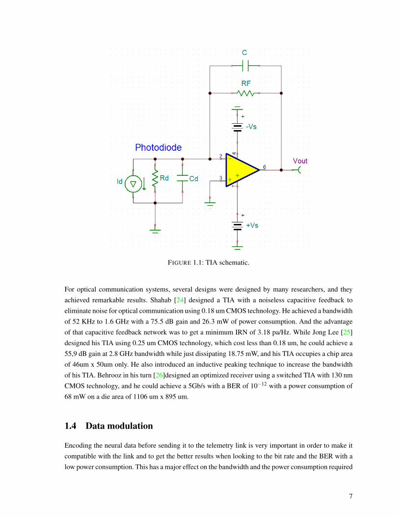
FIGURE 1.1: TIA schematic.
For optical communication systems, several designs were designed by many researchers, and they
achieved remarkable results. Shahab [24] designed a TIA with a noiseless capacitive feedback to
eliminate noise for optical communication using 0.18 um CMOS technology. He achieved a bandwidth
of 52 KHz to 1.6 GHz with a 75.5 dB gain and 26.3 mW of power consumption. And the advantage
of that capacitive feedback network was to get a minimum IRN of 3.18 pa/Hz. While Jong Lee [25]
designed his TIA using 0.25 um CMOS technology, which cost less than 0.18 um, he could achieve a
55,9 dB gain at 2.8 GHz bandwidth while just dissipating 18.75 mW, and his TIA occupies a chip area
of 46um x 50um only. He also introduced an inductive peaking technique to increase the bandwidth
of his TIA. Behrooz in his turn [26]designed an optimized receiver using a switched TIA with 130 nm
CMOS technology, and he could achieve a 5Gb/s with a BER of 10−12 with a power consumption of
68 mW on a die area of 1106 um x 895 um.
1.4 Data modulation
Encoding the neural data before sending it to the telemetry link is very important in order to make it
compatible with the link and to get the better results when looking to the bit rate and the BER with a
low power consumption. This has a major effect on the bandwidth and the power consumption required
7
for the whole system. Different types of data modulation were used widely for the optical transmission,
and each type has its own characteristics. Bandwidth efficiency, power efficiency, spectral efficiency,
clock and data recognition and the BER are the main features of a data modulation used in the optical
system. Thus an efficient data modulation scheme is desired. There are several modulation schemes
that can be compatible with an optical wireless system.
1.4.1 OOK
On-Off keying is One of the simplest modulation techniques that are used widely in optical communi-
cation systems. It is simply implemented by turning ON and OFF the optical transmitter depending on
the serial binary, if we have a 1 the transmitter will turns on when it is 0 the transmitter will turn off.
And this modulation is divided into two general types ; we have the RZ and the NRZ. OOK with RZ in
which the signal drops to zero between each pulse, even if we have two consecutive zeros or ones, this
means that the signal is self-clocking and there is no need for a clock signal to be sent with the signal,
but the main disadvantage is that this scheme required twice the bandwidth to get the same data rate as
the NRZ. Now for the OOK NRZ, it utilizes positive voltage to represent ones and negative voltages
to represent zeros without the use of the rest state, and here we need a clock for the synchronization.
Among those two techniques, the OOK-NRZ is mostly used, the transmitter sends square wave pulses
of duration 1/Rb (where Rb is the bit rate), and an intensity that is equal twice the transmission
power[27] when the bit is one and no pulse when it represents zero.
1.4.2 PPM
Pulse position modulation or also known as pulse phase modulation, it is a form of signal modulation
that has been used widely in wired or wireless fibre-optic communication, RF communication and
occasionally for IR communication because it has a little multi-path interference. In PPM in which
M message bits are encoded by transmitting a single pulse in one of 2M possible required time-shifts
[28] [29], it is repeated every T seconds, such that the transmitted bit rate is M/T bits per second [30].
Each symbol interval of duration T is divided into L chips each of duration T/L, and the transmitter
sends an optical pulse during exclusively one chip. If we have more than two chips, then PPM will
require less power than OOK[27]. Which means for a large number of chips’ L, we have fewer optical
power requirements.
1.4.3 DPIM
DPIM is an "anisochronous pulse time modulation" technique that encodes data into a number of
discrete time intervals between adjacent pulses. The information content of the symbol determines the
symbol length, and to avoid adjacent symbols with zero time between them, we should add a guard
slot to each symbol [2]. This technique offers a higher transmission capacity due to the elimination of
all unused time slots in each symbol, and it requires no symbol synchronization because each symbol
is initiated with a pulse [31].
8
1.4.4 Comparison
As mentioned before OOK is the simplest modulation techniques between them, but they are still not
the best choice for optical data transmission. Let’s start with the power efficiency comparison. From
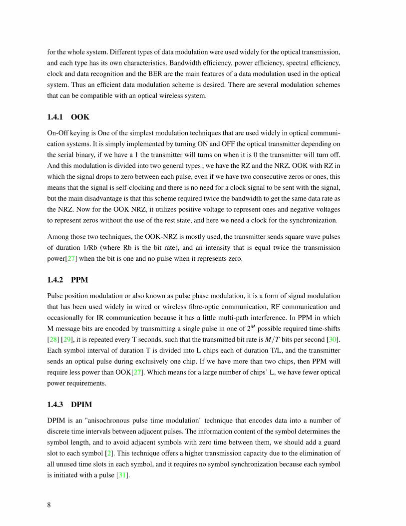
[2] the average power requirement is given by :
Pppm/Pook =dook/dmin =√
2/(L∗Log(L))
So, for L bigger than 2, OOK consume more optical power than PPM.Figure 1.2 shows the comparison
in power efficiency between the three techniques, as we can see OOK has the worst power efficiency,
and DPIM needs little more power than PPM. For example if we take M=5, PPM requires 9.7 dB less
than OOK and approximately 3 dB less than DPIM.
FIGURE 1.2: Transmission power comparison reprinted from[2].
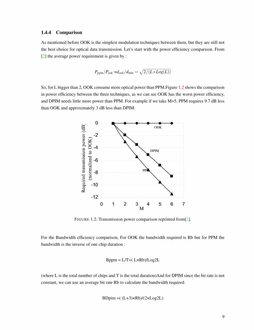
For the Bandwidth efficiency comparison, For OOK the bandwidth required is Rb but for PPM the
bandwidth is the inverse of one chip duration :
Bppm = L/T=( L×Rb)/Log2L
(where L is the total number of chips and T is the total duration)And for DPIM since the bit rate is not
constant, we can use an average bit rate Rb to calculate the bandwidth required.
BDpim =( (L+3)×Rb)/(2×Log2L)
9
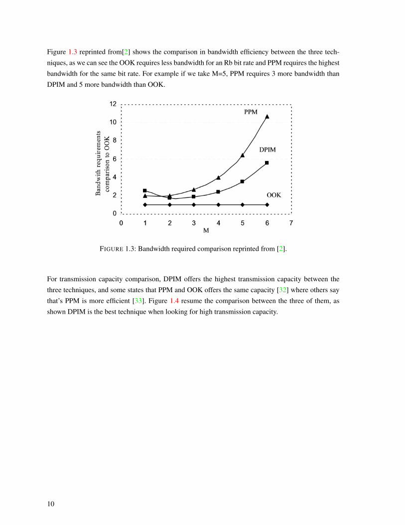
Figure 1.3 reprinted from[2] shows the comparison in bandwidth efficiency between the three tech-
niques, as we can see the OOK requires less bandwidth for an Rb bit rate and PPM requires the highest
bandwidth for the same bit rate. For example if we take M=5, PPM requires 3 more bandwidth than
DPIM and 5 more bandwidth than OOK.
FIGURE 1.3: Bandwidth required comparison reprinted from [2].
For transmission capacity comparison, DPIM offers the highest transmission capacity between the
three techniques, and some states that PPM and OOK offers the same capacity [32] where others say
that’s PPM is more efficient [33]. Figure 1.4 resume the comparison between the three of them, as
shown DPIM is the best technique when looking for high transmission capacity.
10
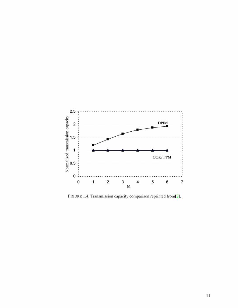
FIGURE 1.4: Transmission capacity comparison reprinted from[2].
11

Chapitre 2
Transcutaneous optical link designmethodology
This chapter fully describes our transcutaneous optical link design methodology, starting by the design
specifications, to the method of transmission used and the reason we used it in comparison to other
methods, the components of the TOL and their properties, the properties of the medium the light is
going through, the obstacles that will faces such as absorption and scattering, and finally state the
optical safety.
2.1 Design specifications
To build the transcutaneous optical link, the design should meet some specifications.
1. The link should be designed wirelessly.
2. The power consumption of the implanted device should be less than 100 mW in order to be
capable to work for a long time and without damaging the tissue.
3. The device should transmit data of high quality for accurate detection, for that a low BER of
10−5 errors/bit is needed.
4. The link should be able to operate at high bit rate for high speed communication.
5. The Link should be able to send data through a sufficiently thick tissue of 3 mm with sufficient
tolerance against misalignment.
6. The optical emitter must not expose the skin to radiation of intensity greater than that allowed
by the ANSI national standards [34].
7. The link should use high-quality components that are commercially available when needed.
So we have to design an optical link which ensures that all the listed specifications are met, so first we
have to select a proper optical transmitter that will be able to deliver the neural signals through the skin
at a high bit rate and with low BER, which will need a special driver with low power consumption.
13
2.2 Method of data transmission
Neural data transmission can be achieved by many ways, even wirelessly or using a percutaneous
link. Starting by the percutaneous link, it demonstrates that this way can achieve remarkable results
in Bandwidth and SNR but the main problem of this method that it needs to cross the skin with some
wires, which can damage the brain and increase the possibility of infection, as we said before we are
looking for a safety way to send those neural data without putting any danger on the patient.
So we have to search for a method that can be done wirelessly without affecting the patient skin. Ad-
ditionally, many methods have been released for such a goal like RF links, Ultra Wide Band (UWB),
Ultrasound or infrared optical light. All of them have some advantages and disadvantages.
RF technology is now used worldwide in most implantable systems. It depends on an antenna that
acts as a transmitter inside the brain and sends data with RF through the brain tissue to an external
receiver, and there has been a huge progress in this field.
[35] has shown that bit rate of several Mbps can be achievable ; they reached 24 Mbps with a power
consumption of 30 mW, which is relatively high to such a Bit Rate. A disadvantage of this transmitting
technology is that it is limited with a specific range of frequencies between 402-405 MHz, which is
known as MICS band and getting a sufficient SNR for the system which can be affected by many
factors, including the transmitter power, the noise coming from other RF sources, the separation of
the transmitter and receiver, and the absorption of the signal by the tissue.
Ultrasonic transmission also affords a large bandwidth but on the other side :
1. The major drawback is the level of miniaturization that the system can achieve.
2. The absence of ultrasonic telemetry component.
3. The high voltage required for this technique. [36]
Optical link could be also useful for our system, due to the large bandwidth that it can afford, minor
interference that could come from other optical sources and the ease of modulation and demodulation.
Optical telemetry link has been used worldwide, first for low data rate transmission to provide data
from neuromuscular stimulators [37] artificial hearts [38] and as well in neural recording systems [39]
[40]. A higher data rate was achievable later showing the possibility of high data rates in optical link
[22] where they achieve 75 Mbps with very low power consumption. All these factors made the optical
transcutaneous link the ideal way for high data rate transcutaneous transmission.
2.3 Essentials of optical communication
After selecting the optical link to be the ideal way for transmitting our neural recorded data through
the brain, the TOL that was constructed is this work depends on many components, techniques and
studies. All the TOLs are similar in the design, he only thing that differs is the components used
14
and the medium of transmission. So it is important to understand and identify every part of this TOL
design.
2.3.1 Optical transmitter
A Semiconductor photo-emitters that converts an electrical signal into an optical signal has to be used
to transmit neural signal from the brain through the skin, such like LED, LD or VCSEL.
These entire optical transmitters can be used, but we have to take into consideration the high speed
and high-power efficiency with large modulation bandwidth. The LED is commonly used in optical
communication due to its wide availability and simplicity with very low-cost and reasonable low
power consumption, but we cannot use it in our case because it has a poor electrical-optical power
efficiency which doesn’t meet our specifications. [41]
Lasers tend to have a better performance than LED when looking to the bandwidth and the electrical-
optical power efficiency but their power efficiency is less than that of the VCSEL.
VCSELs have a very large modulation bandwidth and are becoming truly common in optical com-
munication, but the main disadvantage is that it costs a bit higher than other components but it is
still considered as low cost component. Now the emitter wavelength is quite important and should be
chosen to maximize power transfer through the skin, which means we have to limit absorption and
scattering coefficient. The skin does scatter and absorbs light but wavelengths in the range of 750-1300
nm represents a “skin optical window” where absorption and scattering are minimal [42].
For that we choose an 850 nm VCSEL because its wavelength is in the optimal range, and it is the
wavelength at which efficient VCSEL is manufactured, so the operation at this wavelength ensures the
highest power efficiency possible.
2.3.2 Optical receiver
Semiconductor photo detectors convert an optical signal into an electrical signal. There is a large
number of photo detectors that can be used in optical communication, including the p-n photodiode,
the p-i-n photodiode, the metal-semiconductor photodiode and the avalanche photodiode [43].
The photodiode selected for a TOL should have a bandwidth sufficient for the data rate needed and
should have a large active area to compensate the misalignment effects and to collect as much as pos-
sible of scattering light.
P-i-n photodiode was chosen for the TOL because its most commonly used photo-detector for optical
communications, it’s inexpensive, has a large optically responsive area and generally has a high quan-
tum efficiency.
There is a high need for an amplifier to amplify the electrical signal from the Photodiode for getting a
clean and clear signal to be able to distinguish between the zeros and ones in the digital data.
15

2.3.3 Skin and misalignment effects
Any medium through which light propagate absorbs and scatters photons, except for a complete va-
cuum space. Accurate understanding for the optical properties of the human skin still a challenge to
biomedical optics, but we know when light propagates through the skin, it will be significantly absor-
bed and scattered by the layer of the human skin that we will describe in details in the next section ;
those effects on the light vary with the thickness of the tissue.
All these factors affect the amount of efficient power transferred through the skin. Another factor is
the misalignment between transmitter and the receiver, for that the two of them should be perfectly
aligned, and a design should be tolerant of some misalignment because when a patient wants to put
his own device, it won’t be placed with high accuracy and no misalignment. This design could be
done with several methods to tolerate misalignment, either by increasing the size of the photo-diode
so it can capture more propagating photons, or by increasing the power of the transmitter which is not
a very good idea, or by using optical cleaning, which is a non-well known method that we will talk
about later.
2.4 Skin’s Optical properties
As mentioned before, human skin layers greatly affect the distribution and the path of light propagating
from the transmitter to the receiving photo-diode, it’s important to understand the optical property of
the medium light is propagating through and to clearly identify the amount of light absorbed and
scattered before reaching the receiver. For that we are going to state the structure of the human skin
and its effect at different wavelengths.
2.4.1 Human skin layers
The skin consists of three primary layers of tissue and each of these layers is divided into several
layers [3] as shown in Figure 2.1 :
1. The epidermis : an outermost layer that contains the primary protective structure, the stratum
corneum.
2. The dermis : a fibrous layer that supports and strengthens the epidermis.
3. The subcutis : a subcutaneous layer of fat beneath the dermis that supplies nutrients to the other
two layers and that cushions and insulates the body.
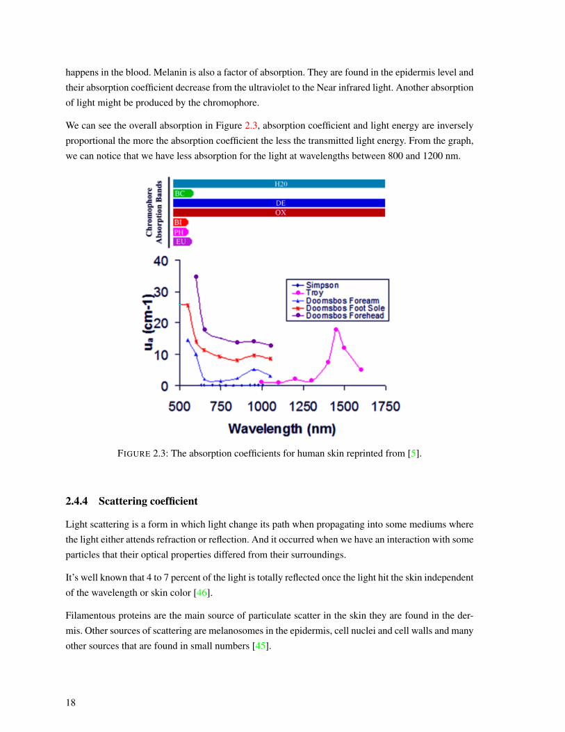
2.4.2 Chromophores effects
Human skin, especially the epidermis, contains several major chromophores including DNA, urocanic
acid, amino acids, melanins and their precursors and metabolites, that absorb light in the visible or
near IR spectrum. These chromophores tend to have a higher absorption coefficients for the shorter
wavelength [44] as shown in Figure 2.2
16
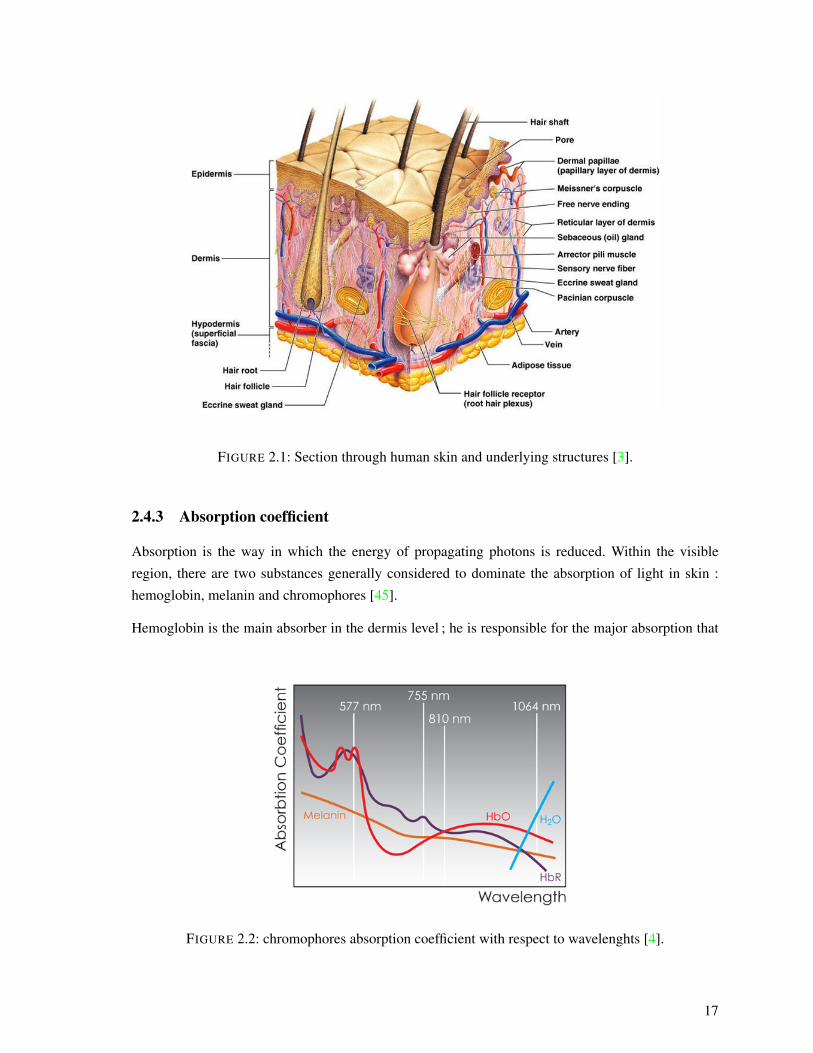
FIGURE 2.1: Section through human skin and underlying structures [3].
2.4.3 Absorption coefficient
Absorption is the way in which the energy of propagating photons is reduced. Within the visible
region, there are two substances generally considered to dominate the absorption of light in skin :
hemoglobin, melanin and chromophores [45].
Hemoglobin is the main absorber in the dermis level ; he is responsible for the major absorption that
FIGURE 2.2: chromophores absorption coefficient with respect to wavelenghts [4].
17
happens in the blood. Melanin is also a factor of absorption. They are found in the epidermis level and
their absorption coefficient decrease from the ultraviolet to the Near infrared light. Another absorption
of light might be produced by the chromophore.
We can see the overall absorption in Figure 2.3, absorption coefficient and light energy are inversely
proportional the more the absorption coefficient the less the transmitted light energy. From the graph,
we can notice that we have less absorption for the light at wavelengths between 800 and 1200 nm.
FIGURE 2.3: The absorption coefficients for human skin reprinted from [5].
2.4.4 Scattering coefficient
Light scattering is a form in which light change its path when propagating into some mediums where
the light either attends refraction or reflection. And it occurred when we have an interaction with some
particles that their optical properties differed from their surroundings.
It’s well known that 4 to 7 percent of the light is totally reflected once the light hit the skin independent
of the wavelength or skin color [46].
Filamentous proteins are the main source of particulate scatter in the skin they are found in the der-
mis. Other sources of scattering are melanosomes in the epidermis, cell nuclei and cell walls and many
other sources that are found in small numbers [45].
18
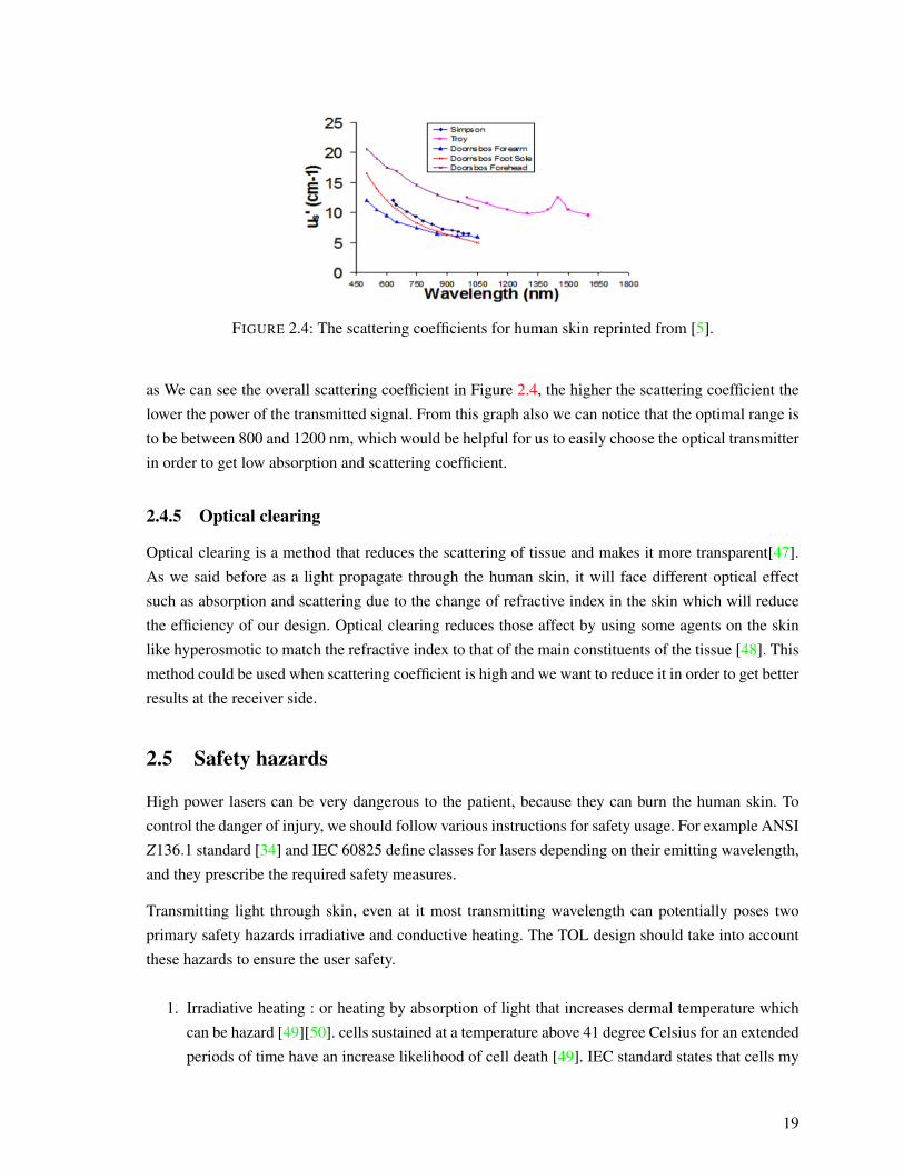
FIGURE 2.4: The scattering coefficients for human skin reprinted from [5].
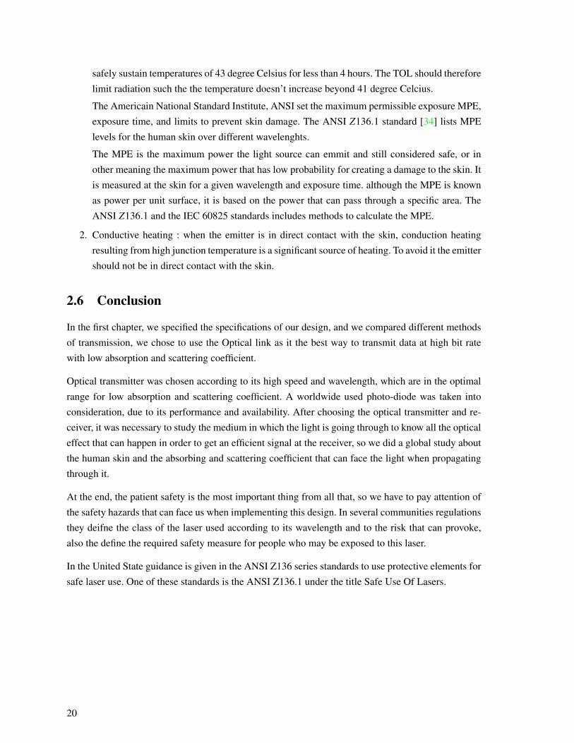
as We can see the overall scattering coefficient in Figure 2.4, the higher the scattering coefficient the
lower the power of the transmitted signal. From this graph also we can notice that the optimal range is
to be between 800 and 1200 nm, which would be helpful for us to easily choose the optical transmitter
in order to get low absorption and scattering coefficient.
2.4.5 Optical clearing
Optical clearing is a method that reduces the scattering of tissue and makes it more transparent[47].
As we said before as a light propagate through the human skin, it will face different optical effect
such as absorption and scattering due to the change of refractive index in the skin which will reduce
the efficiency of our design. Optical clearing reduces those affect by using some agents on the skin
like hyperosmotic to match the refractive index to that of the main constituents of the tissue [48]. This
method could be used when scattering coefficient is high and we want to reduce it in order to get better
results at the receiver side.
2.5 Safety hazards
High power lasers can be very dangerous to the patient, because they can burn the human skin. To
control the danger of injury, we should follow various instructions for safety usage. For example ANSI
Z136.1 standard [34] and IEC 60825 define classes for lasers depending on their emitting wavelength,
and they prescribe the required safety measures.
Transmitting light through skin, even at it most transmitting wavelength can potentially poses two
primary safety hazards irradiative and conductive heating. The TOL design should take into account
these hazards to ensure the user safety.
1. Irradiative heating : or heating by absorption of light that increases dermal temperature which
can be hazard [49][50]. cells sustained at a temperature above 41 degree Celsius for an extended
periods of time have an increase likelihood of cell death [49]. IEC standard states that cells my
19
safely sustain temperatures of 43 degree Celsius for less than 4 hours. The TOL should therefore
limit radiation such the the temperature doesn’t increase beyond 41 degree Celcius.
The Americain National Standard Institute, ANSI set the maximum permissible exposure MPE,
exposure time, and limits to prevent skin damage. The ANSI Z136.1 standard [34] lists MPE
levels for the human skin over different wavelenghts.
The MPE is the maximum power the light source can emmit and still considered safe, or in
other meaning the maximum power that has low probability for creating a damage to the skin. It
is measured at the skin for a given wavelength and exposure time. although the MPE is known
as power per unit surface, it is based on the power that can pass through a specific area. The
ANSI Z136.1 and the IEC 60825 standards includes methods to calculate the MPE.
2. Conductive heating : when the emitter is in direct contact with the skin, conduction heating
resulting from high junction temperature is a significant source of heating. To avoid it the emitter
should not be in direct contact with the skin.
2.6 Conclusion
In the first chapter, we specified the specifications of our design, and we compared different methods
of transmission, we chose to use the Optical link as it the best way to transmit data at high bit rate
with low absorption and scattering coefficient.
Optical transmitter was chosen according to its high speed and wavelength, which are in the optimal
range for low absorption and scattering coefficient. A worldwide used photo-diode was taken into
consideration, due to its performance and availability. After choosing the optical transmitter and re-
ceiver, it was necessary to study the medium in which the light is going through to know all the optical
effect that can happen in order to get an efficient signal at the receiver, so we did a global study about
the human skin and the absorbing and scattering coefficient that can face the light when propagating
through it.
At the end, the patient safety is the most important thing from all that, so we have to pay attention of
the safety hazards that can face us when implementing this design. In several communities regulations
they deifne the class of the laser used according to its wavelength and to the risk that can provoke,
also the define the required safety measure for people who may be exposed to this laser.
In the United State guidance is given in the ANSI Z136 series standards to use protective elements for
safe laser use. One of these standards is the ANSI Z136.1 under the title Safe Use Of Lasers.
20
Chapitre 3
Integrated Link Design Using 0.18 umCMOS Technology
3.1 CMOS Transimpedance Amplifier
Light detectors have been used significantly during the last period. They convert light or the change of
light into a current. As in my project the goal is to receive the data from the VCSEL and convert it to
digital data thats meant that a typical instrumentation included a Light source (VCSEL) and a Photo-
detector. However, the photo-detector convert light into a small current, so we need to amplify this
current and convert it to a readable voltage, here it comes the need of a Transimpedance amplifier with
a good gain and a sufficient bandwidth. TIA is a current to voltage converter, most often implemented
using an operational amplifier. The TIA can be used to amplify the current output of photo detectors
and other types of sensors and convert it to a sufficient voltage.
Nowadays, CMOS technology has turned out to be the leading technology in circuit design due to its
striking advantages of high scaling factor, low power, and low cost [1]. These advantages of CMOS
technology have motivated work in high speed circuit designs, especially in optical transceivers where
high speed is recommended. Optical sensors have been used significantly during the last period. Ty-
pical instrumentation includes a Light source (VCSEL), a Photo-detector PD and an amplifier. TIA
designs face challenges due to the trade off between gain/noise and linearity performances. Different
topologies are considered to achieve high performances [51]. Now for the PD current, high gain with
high bandwidth and low noise is required. Among various TIA, the current mode TIA is the most
commonly used topology. Typically, the current-mode TIA uses current mirror topology, for the input
stage to sustain small input impedance and high bandwidth. Fig 3.1 shows the current mode topology.
It is attractive for wide bandwidth TIA design since stability is not an issue [6].
In this part, a TIA that converts the photo-current and converts it to a usable voltage signal with a
sufficient bandwidth, low power consumption and low input-referred noise that fit our system is to be
designed and simulated.
21
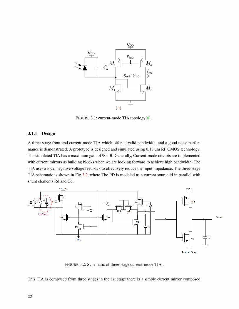
FIGURE 3.1: current-mode TIA topology[6] .
3.1.1 Design
A three-stage front-end current-mode TIA which offers a valid bandwidth, and a good noise perfor-
mance is demonstrated. A prototype is designed and simulated using 0.18 um RF CMOS technology.
The simulated TIA has a maximum gain of 90 dB. Generally, Current-mode circuits are implemented
with current mirrors as building blocks when we are looking forward to achieve high bandwidth. The
TIA uses a local negative voltage feedback to effectively reduce the input impedance. The three-stage
TIA schematic is shown in Fig 3.2, where The PD is modeled as a current source id in parallel with
shunt elements Rd and Cd.
FIGURE 3.2: Schematic of three-stage current-mode TIA .
This TIA is composed from three stages in the 1st stage there is a simple current mirror composed
22
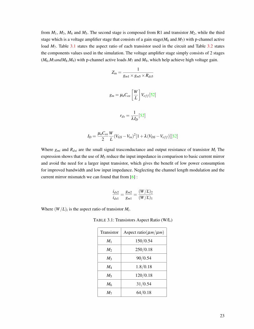
from M1, M3, M4 and M5. The second stage is composed from R1 and transistor M2, while the third
stage which is a voltage amplifier stage that consists of a gain stage(M6 and M7) with p-channel active
load M7. Table 3.1 states the aspect ratio of each transistor used in the circuit and Table 3.2 states
the components values used in the simulation. The voltage amplifier stage simply consists of 2 stages
(M6,M7andM8,M9) with p-channel active loads M7 and M9, which help achieve high voltage gain.
Zin =1
gm1×gm5×Rds5
gm = µnCox
[WL
]Ve f f [52]
rds =1
λ ID[52]
ID =µnCox
2WL(VGS−Vtn)
2[1+λ (VDS−Ve f f )][52]
Where gmi and Rdsi are the small signal trasconductance and output resistance of transistor Mi The
expression shows that the use of M5 reduce the input impedance in comparison to basic current mirror
and avoid the need for a larger input transistor, which gives the benefit of low power consumption
for improved bandwidth and low input impedance. Neglecting the channel length modulation and the
current mirror mismatch we can found that from [6] :
ids2
ids1=
gm2
gm1=
(W/L)2
(W/L)1
Where (W/L)i is the aspect ratio of transistor Mi.
TABLE 3.1: Transistors Aspect Ratio (W/L)
Transistor Aspect ratio(µm/µm)
M1 150/0.54
M2 250/0.18
M3 90/0.54
M4 1.8/0.18
M5 120/0.18
M6 31/0.54
M7 64/0.18
23
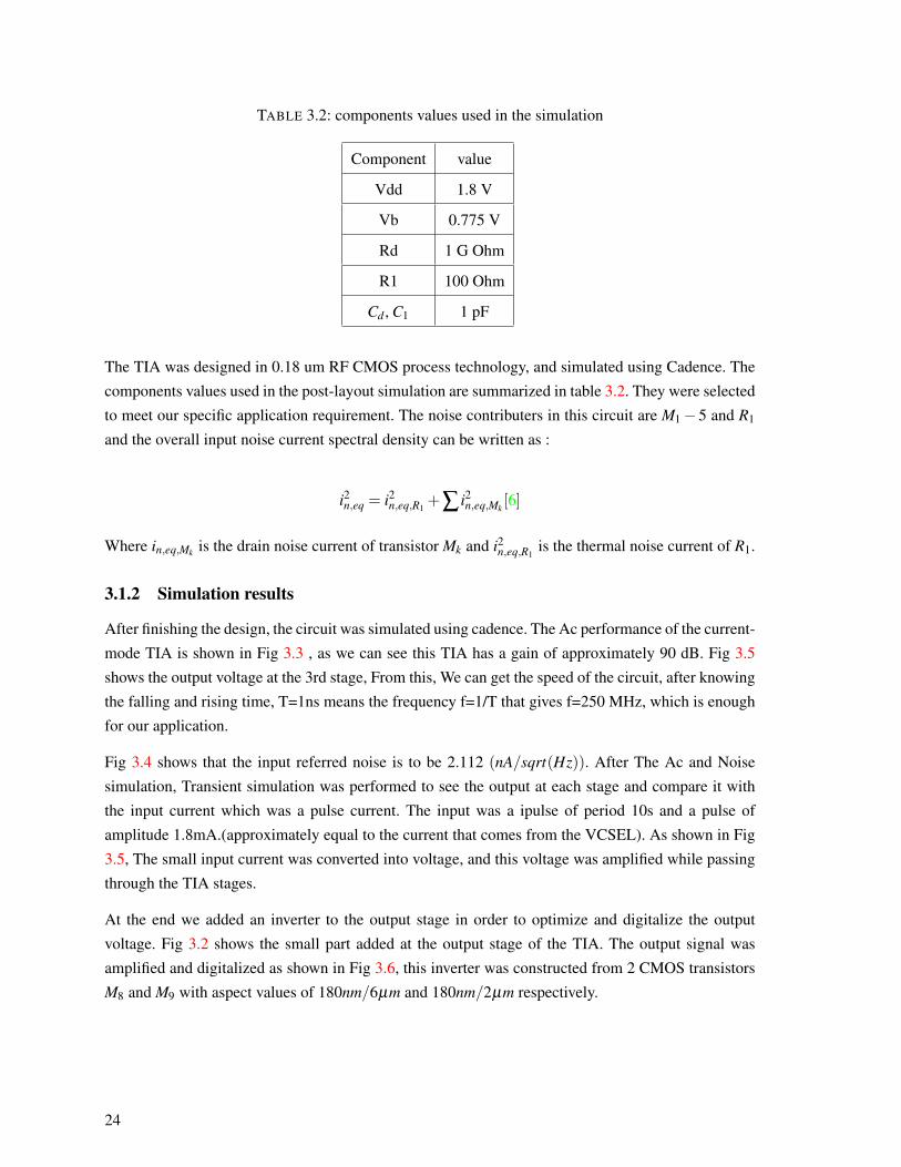
TABLE 3.2: components values used in the simulation
Component value
Vdd 1.8 V
Vb 0.775 V
Rd 1 G Ohm
R1 100 Ohm
Cd , C1 1 pF
The TIA was designed in 0.18 um RF CMOS process technology, and simulated using Cadence. The
components values used in the post-layout simulation are summarized in table 3.2. They were selected
to meet our specific application requirement. The noise contributers in this circuit are M1−5 and R1
and the overall input noise current spectral density can be written as :
i2n,eq = i2n,eq,R1+∑ i2n,eq,Mk
[6]
Where in,eq,Mk is the drain noise current of transistor Mk and i2n,eq,R1is the thermal noise current of R1.
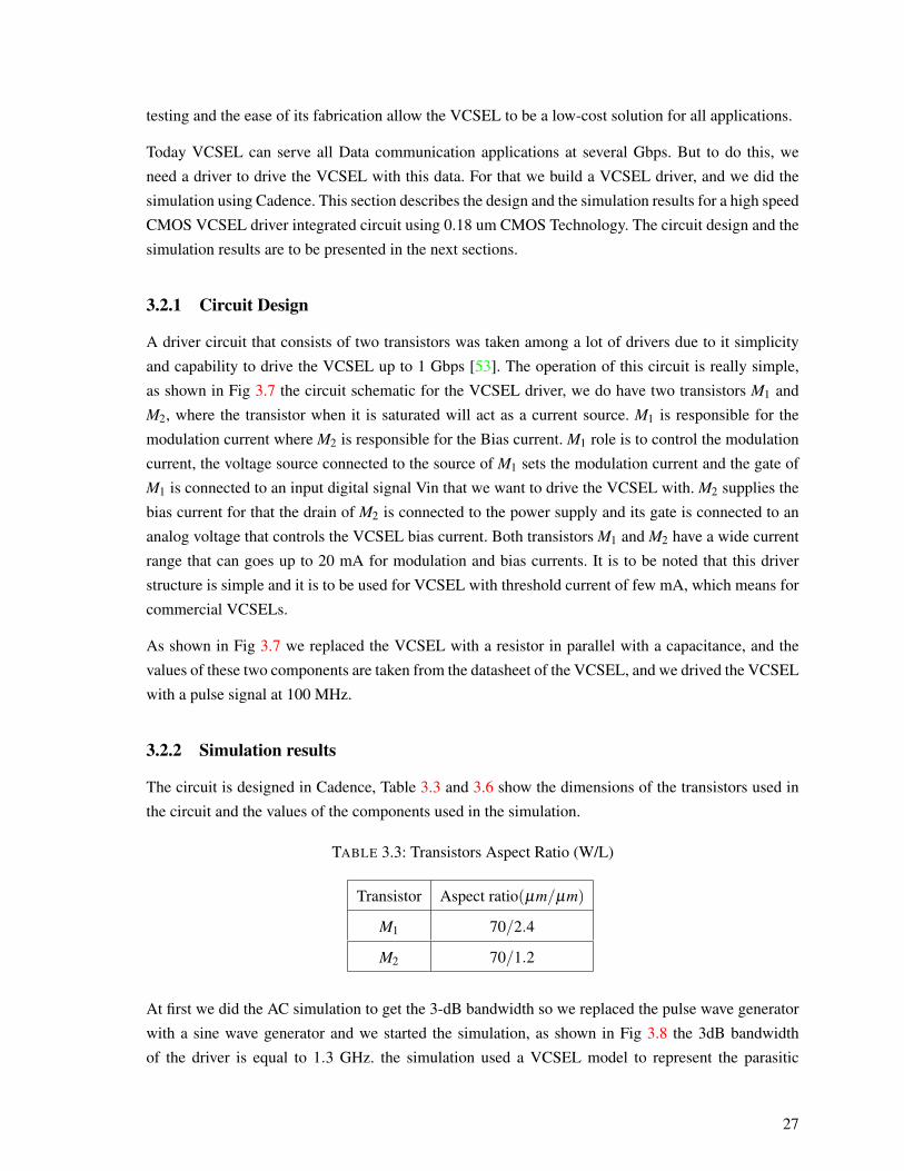
3.1.2 Simulation results
After finishing the design, the circuit was simulated using cadence. The Ac performance of the current-
mode TIA is shown in Fig 3.3 , as we can see this TIA has a gain of approximately 90 dB. Fig 3.5
shows the output voltage at the 3rd stage, From this, We can get the speed of the circuit, after knowing
the falling and rising time, T=1ns means the frequency f=1/T that gives f=250 MHz, which is enough
for our application.
Fig 3.4 shows that the input referred noise is to be 2.112 (nA/sqrt(Hz)). After The Ac and Noise
simulation, Transient simulation was performed to see the output at each stage and compare it with
the input current which was a pulse current. The input was a ipulse of period 10s and a pulse of
amplitude 1.8mA.(approximately equal to the current that comes from the VCSEL). As shown in Fig
3.5, The small input current was converted into voltage, and this voltage was amplified while passing
through the TIA stages.
At the end we added an inverter to the output stage in order to optimize and digitalize the output
voltage. Fig 3.2 shows the small part added at the output stage of the TIA. The output signal was
amplified and digitalized as shown in Fig 3.6, this inverter was constructed from 2 CMOS transistors
M8 and M9 with aspect values of 180nm/6µm and 180nm/2µm respectively.
24
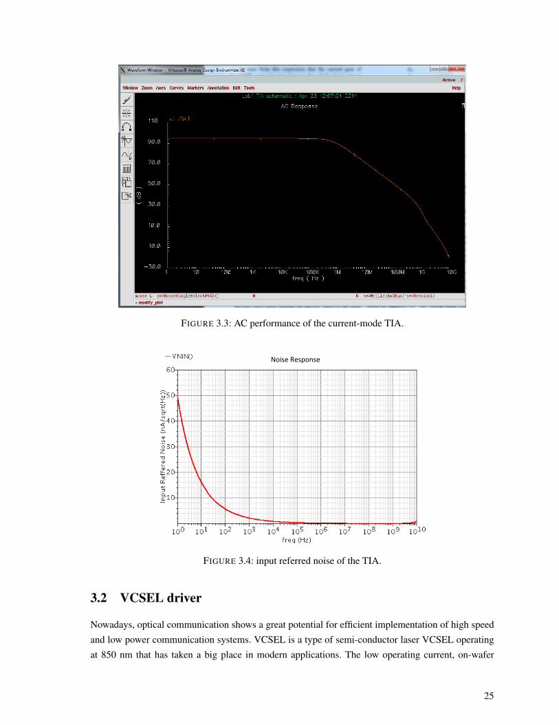
FIGURE 3.3: AC performance of the current-mode TIA.
Noise Response
FIGURE 3.4: input referred noise of the TIA.
3.2 VCSEL driver
Nowadays, optical communication shows a great potential for efficient implementation of high speed
and low power communication systems. VCSEL is a type of semi-conductor laser VCSEL operating
at 850 nm that has taken a big place in modern applications. The low operating current, on-wafer
25
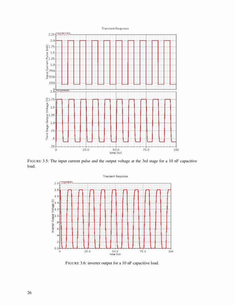
FIGURE 3.5: The input current pulse and the output voltage at the 3rd stage for a 10 nF capacitiveload.
FIGURE 3.6: inverter output for a 10 nF capacitive load.
26
testing and the ease of its fabrication allow the VCSEL to be a low-cost solution for all applications.
Today VCSEL can serve all Data communication applications at several Gbps. But to do this, we
need a driver to drive the VCSEL with this data. For that we build a VCSEL driver, and we did the
simulation using Cadence. This section describes the design and the simulation results for a high speed
CMOS VCSEL driver integrated circuit using 0.18 um CMOS Technology. The circuit design and the
simulation results are to be presented in the next sections.
3.2.1 Circuit Design
A driver circuit that consists of two transistors was taken among a lot of drivers due to it simplicity
and capability to drive the VCSEL up to 1 Gbps [53]. The operation of this circuit is really simple,
as shown in Fig 3.7 the circuit schematic for the VCSEL driver, we do have two transistors M1 and
M2, where the transistor when it is saturated will act as a current source. M1 is responsible for the
modulation current where M2 is responsible for the Bias current. M1 role is to control the modulation
current, the voltage source connected to the source of M1 sets the modulation current and the gate of
M1 is connected to an input digital signal Vin that we want to drive the VCSEL with. M2 supplies the
bias current for that the drain of M2 is connected to the power supply and its gate is connected to an
analog voltage that controls the VCSEL bias current. Both transistors M1 and M2 have a wide current
range that can goes up to 20 mA for modulation and bias currents. It is to be noted that this driver
structure is simple and it is to be used for VCSEL with threshold current of few mA, which means for
commercial VCSELs.
As shown in Fig 3.7 we replaced the VCSEL with a resistor in parallel with a capacitance, and the
values of these two components are taken from the datasheet of the VCSEL, and we drived the VCSEL
with a pulse signal at 100 MHz.
3.2.2 Simulation results
The circuit is designed in Cadence, Table 3.3 and 3.6 show the dimensions of the transistors used in
the circuit and the values of the components used in the simulation.
TABLE 3.3: Transistors Aspect Ratio (W/L)
Transistor Aspect ratio(µm/µm)
M1 70/2.4
M2 70/1.2
At first we did the AC simulation to get the 3-dB bandwidth so we replaced the pulse wave generator
with a sine wave generator and we started the simulation, as shown in Fig 3.8 the 3dB bandwidth
of the driver is equal to 1.3 GHz. the simulation used a VCSEL model to represent the parasitic
27
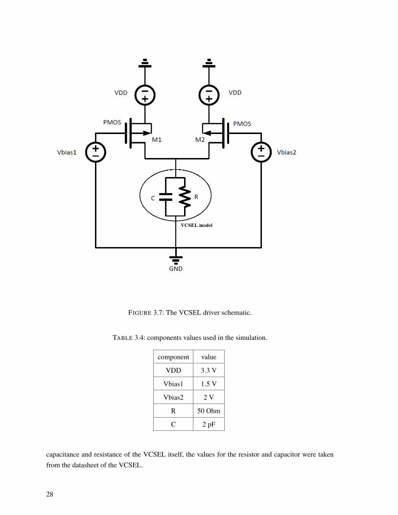
FIGURE 3.7: The VCSEL driver schematic.
TABLE 3.4: components values used in the simulation.
component value
VDD 3.3 V
Vbias1 1.5 V
Vbias2 2 V
R 50 Ohm
C 2 pF
capacitance and resistance of the VCSEL itself, the values for the resistor and capacitor were taken
from the datasheet of the VCSEL.
28
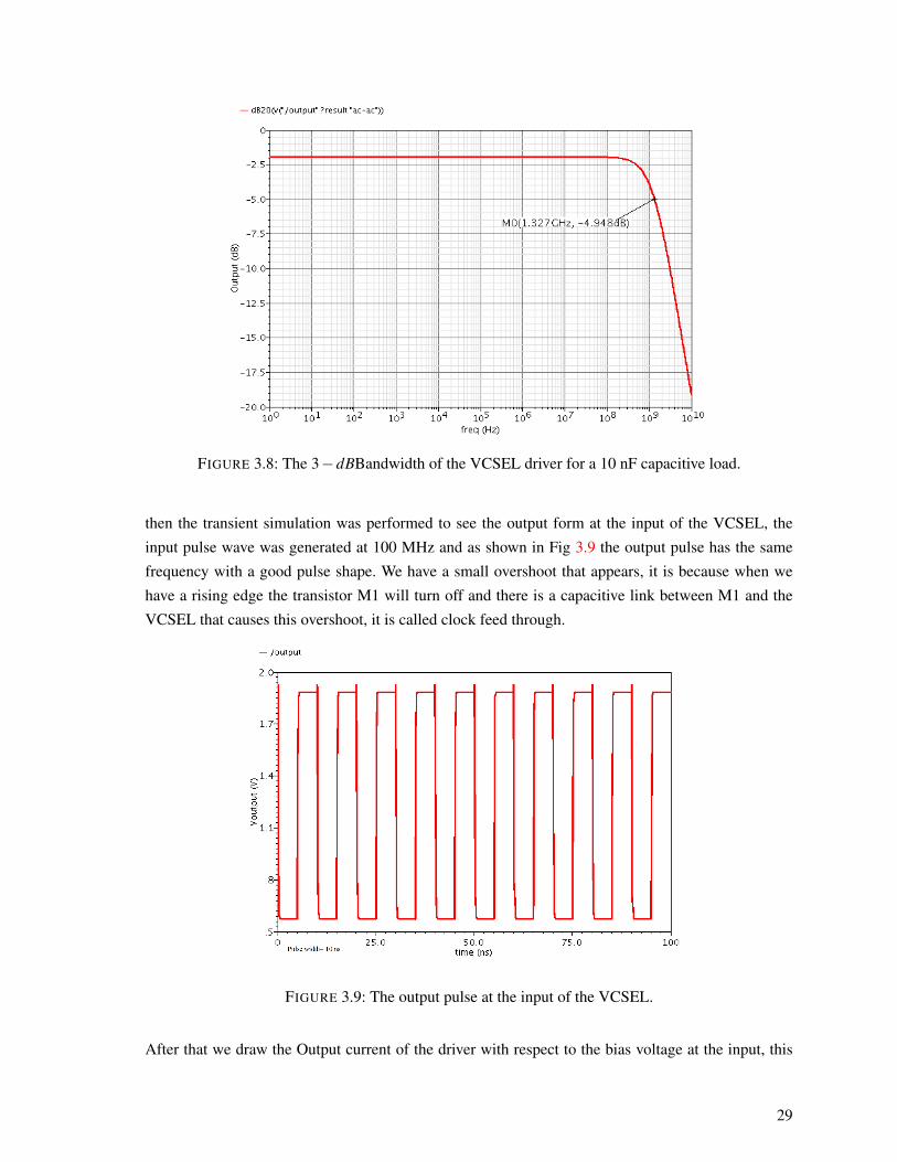
FIGURE 3.8: The 3−dBBandwidth of the VCSEL driver for a 10 nF capacitive load.
then the transient simulation was performed to see the output form at the input of the VCSEL, the
input pulse wave was generated at 100 MHz and as shown in Fig 3.9 the output pulse has the same
frequency with a good pulse shape. We have a small overshoot that appears, it is because when we
have a rising edge the transistor M1 will turn off and there is a capacitive link between M1 and the
VCSEL that causes this overshoot, it is called clock feed through.
FIGURE 3.9: The output pulse at the input of the VCSEL.
After that we draw the Output current of the driver with respect to the bias voltage at the input, this
29
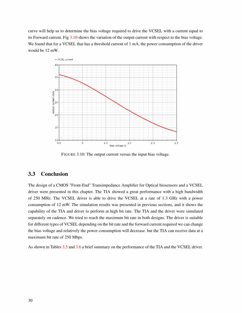
curve will help us to determine the bias voltage required to drive the VCSEL with a current equal to
its Forward current. Fig 3.10 shows the variation of the output current with respect to the bias voltage.
We found that for a VCSEL that has a threshold current of 1 mA, the power consumption of the driver
would be 12 mW.
FIGURE 3.10: The output current versus the input bias voltage.
3.3 Conclusion
The design of a CMOS "Front-End" Transimpedance Amplifier for Optical biosensors and a VCSEL
driver were presented in this chapter. The TIA showed a great performance with a high bandwidth
of 250 MHz. The VCSEL driver is able to drive the VCSEL at a rate of 1.3 GHz with a power
consumption of 12 mW. The simulation results was presented in previous sections, and it shows the
capability of the TIA and driver to perform at high bit rate. The TIA and the driver were simulated
separately on cadence. We tried to reach the maximum bit rate in both designs. The driver is suitable
for different types of VCSEL depending on the bit rate and the forward current required we can change
the bias voltage and relatively the power consumption will decrease. but the TIA can receive data at a
maximum bit rate of 250 Mbps.
As shown in Tables 3.5 and 3.6 a brief summary on the performance of the TIA and the VCSEL driver.
30
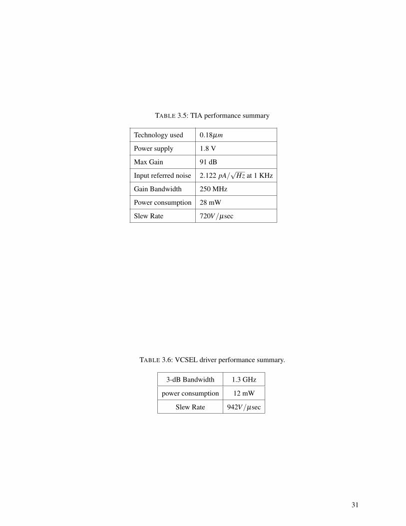
TABLE 3.5: TIA performance summary
Technology used 0.18µm
Power supply 1.8 V
Max Gain 91 dB
Input referred noise 2.122 pA/√
Hz at 1 KHz
Gain Bandwidth 250 MHz
Power consumption 28 mW
Slew Rate 720V/µsec
TABLE 3.6: VCSEL driver performance summary.
3-dB Bandwidth 1.3 GHz
power consumption 12 mW
Slew Rate 942V/µsec
31

Chapitre 4
Discrete Link Design
4.1 Introduction
The need for a high bit rate with low power consumption increases the number of researchers in this
domain using different methods trying to achieve the best bit rate and power consumption ratio. As
mentioned before data transmission can be done with several methods, it can be percutaneous, which
is unsuitable and may cause damage to the skin, or wirelessly which is a better way not to put the
skin in danger. For the transcutaneous optical link ; the design of the driver, the optical transmitters
chosen and the Photodiode used in the receiver side are the main factors for achieving good results for
high data rate and low power consumption. First, we chose the transmitter to be used considering the
wavelength, the speed of transmission and the forward current needed to turn ON of this transmitter,
then we designed a suitable driver that doesnt consume much power and has a high switching speed,
and finally we picked up the photodiode for the receiver side that has the same wavelength of the
transmitter with a sufficient speed of switching and a large active area to be able to receive as much as
possible of the transmitted light. In this chapter, we will describe the design of the optical link which
is capable of transmit data at a rate of 20 Mbps generated normally from the cortical microelectrode
recording array but in this project, we are just using the signal generator because of the absence of
some neural data. This chapter presents the design specifications and includes simulation to know
the BER of the system. The experiment was made with a pork tissue of 3 mm thickness, and the
system shows the ability of transmitting data at a rate of 20 Mbps with a sufficient BER and a power
consumption of 10 mW, which satisfy the system specifications for a high bit rate and a low-power
consumption.
4.2 Link Design
4.2.1 Transmitter
In our optical link, it is important to take into consideration the transmitter size that will be implemen-
ted in the brain and its power consumption. For that a simple VCSEL driver is to be designed and a
33
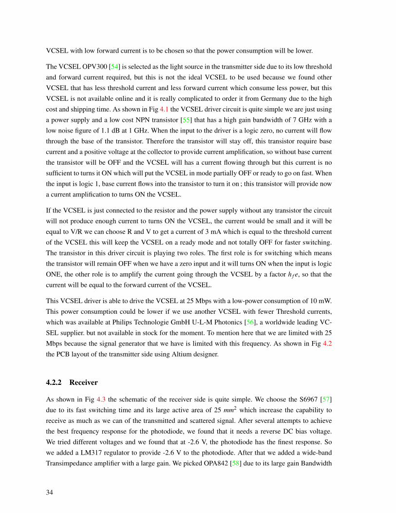
VCSEL with low forward current is to be chosen so that the power consumption will be lower.
The VCSEL OPV300 [54] is selected as the light source in the transmitter side due to its low threshold
and forward current required, but this is not the ideal VCSEL to be used because we found other
VCSEL that has less threshold current and less forward current which consume less power, but this
VCSEL is not available online and it is really complicated to order it from Germany due to the high
cost and shipping time. As shown in Fig 4.1 the VCSEL driver circuit is quite simple we are just using
a power supply and a low cost NPN transistor [55] that has a high gain bandwidth of 7 GHz with a
low noise figure of 1.1 dB at 1 GHz. When the input to the driver is a logic zero, no current will flow
through the base of the transistor. Therefore the transistor will stay off, this transistor require base
current and a positive voltage at the collector to provide current amplification, so without base current
the transistor will be OFF and the VCSEL will has a current flowing through but this current is no
sufficient to turns it ON which will put the VCSEL in mode partially OFF or ready to go on fast. When
the input is logic 1, base current flows into the transistor to turn it on ; this transistor will provide now
a current amplification to turns ON the VCSEL.
If the VCSEL is just connected to the resistor and the power supply without any transistor the circuit
will not produce enough current to turns ON the VCSEL, the current would be small and it will be
equal to V/R we can choose R and V to get a current of 3 mA which is equal to the threshold current
of the VCSEL this will keep the VCSEL on a ready mode and not totally OFF for faster switching.
The transistor in this driver circuit is playing two roles. The first role is for switching which means
the transistor will remain OFF when we have a zero input and it will turns ON when the input is logic
ONE, the other role is to amplify the current going through the VCSEL by a factor h f e, so that the
current will be equal to the forward current of the VCSEL.
This VCSEL driver is able to drive the VCSEL at 25 Mbps with a low-power consumption of 10 mW.
This power consumption could be lower if we use another VCSEL with fewer Threshold currents,
which was available at Philips Technologie GmbH U-L-M Photonics [56], a worldwide leading VC-
SEL supplier. but not available in stock for the moment. To mention here that we are limited with 25
Mbps because the signal generator that we have is limited with this frequency. As shown in Fig 4.2
the PCB layout of the transmitter side using Altium designer.
4.2.2 Receiver
As shown in Fig 4.3 the schematic of the receiver side is quite simple. We choose the S6967 [57]
due to its fast switching time and its large active area of 25 mm2 which increase the capability to
receive as much as we can of the transmitted and scattered signal. After several attempts to achieve
the best frequency response for the photodiode, we found that it needs a reverse DC bias voltage.
We tried different voltages and we found that at -2.6 V, the photodiode has the finest response. So
we added a LM317 regulator to provide -2.6 V to the photodiode. After that we added a wide-band
Transimpedance amplifier with a large gain. We picked OPA842 [58] due to its large gain Bandwidth
34
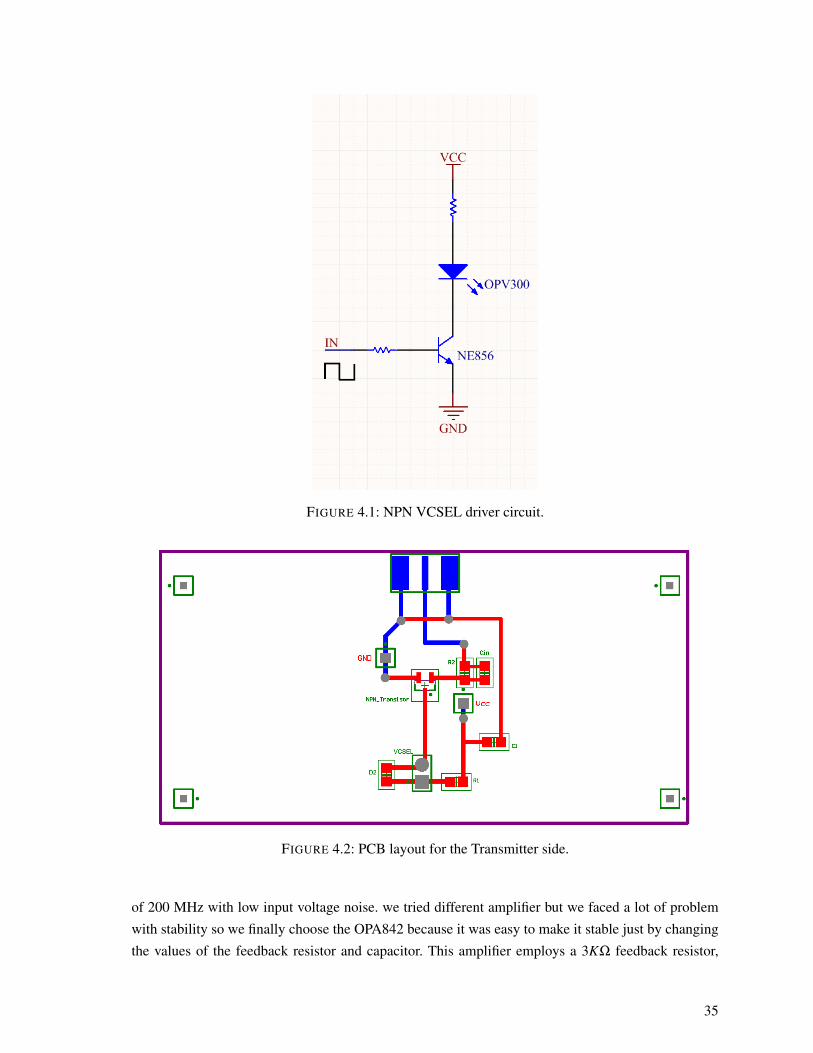
FIGURE 4.1: NPN VCSEL driver circuit.
FIGURE 4.2: PCB layout for the Transmitter side.
of 200 MHz with low input voltage noise. we tried different amplifier but we faced a lot of problem
with stability so we finally choose the OPA842 because it was easy to make it stable just by changing
the values of the feedback resistor and capacitor. This amplifier employs a 3KΩ feedback resistor,
35
combined with a small capacitor in parallel to stabilize the feedback system. Fig 4.4 represents the
PCB layout for the receiver side in altium designer and table states the values of the used components.
FIGURE 4.3: Receiver side schematic.
FIGURE 4.4: PCB layout for the receiver side.
TABLE 4.1: components values used in the circuit.
component RF R2,3 R4 CF C2,3,4,5
Value 3.3KΩ 1KΩ 10KΩ 2 pF 47 uF
4.3 Experimental setup
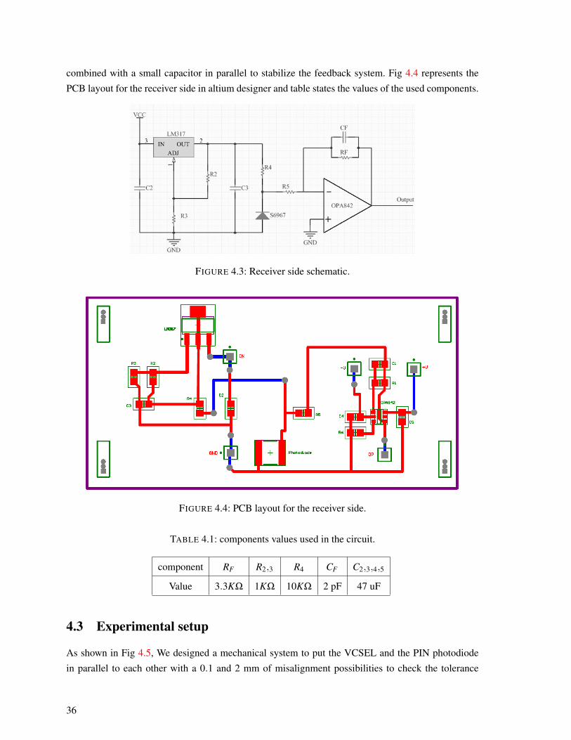
As shown in Fig 4.5, We designed a mechanical system to put the VCSEL and the PIN photodiode
in parallel to each other with a 0.1 and 2 mm of misalignment possibilities to check the tolerance
36
to the misalignment of this link. The distance that separates them can be changed from 2mm to 6mm
depending on the thickness of the pork tissue that will be hold between the transmitter and the receiver.
FIGURE 4.5: The builded symstem to align The VCSEL and the Photodiode.
A mechanical system was constructed in our laboratory with the help of our technicians, 2 PCBS of
the same size for the transmitter, and the receiver were designed. We designed two big PCBs just
for the measurements because we want to test the link at different misalignment between VCSEL
and Photodiode, otherwise the Transmitter size would be very small of 3x3 mm2. The location of
the transmitter and Receiver is the same on both PCBs so that we can ensure that they are perfectly
aligned. We added 3 extra pins to the receiver PCB of 1mm separating distance so that we can change
the position of the transmitter in order to have 1, 2 and 3mm of misalignment. We used big pins so that
we can also change the separating distance between the transmitter and receiver, it can vary between
1 and 6mm. As you can see in Fig 4.6, We can switch the pins between those 3 holes to get 1 and 2
mm of misalignment.
4.4 Experimental Results
At first, we bought a fresh pork skin of 3 mm and we put it between the VCSEL and the photodiode.
This skin should be in contact with the VCSEL. We choose pork skin due to its resemblance to the
human skin as mentioned before in chapter 2. We started with 0 mm of misalignment and the distance
to separate the VCSEL from the Photodiode was 6mm.
After the simulation, we found that at a rate of 20 Mbps the link could send and receive data at a BER
of 10−5, and with 1 and 2mm misalignment tolerance. For the 3mm of misalignment the BER tends
to be bigger but the bit rate and the power consumption remain the same. we had a 20 Mbps with a
BER of 10−3. We were limited with these numbers due to the unavailability to the desired VCSEL
that consumes much less power and achieves higher bit rate.
37
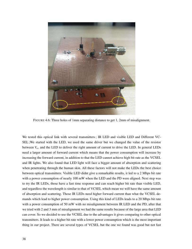
FIGURE 4.6: Three holes of 1mm separating distance to get 1, 2mm of misalignment.
We tested this optical link with several transmitters ; IR LED and visible LED and Different VC-
SEL ;We started with the LED, we used the same driver but we changed the value of the resistor
between Vcc and the LED to deliver the right amount of current to drive the LED. In general LEDs
need a larger amount of forward current which means that the power consumption will increase by
increasing the forward current, in addition to that the LED cannot achieve high bit rate as the VCSEL
and IR lights. We also found that LED light will face a bigger amount of absorption and scattering
when penetrating through the human skin. All these factors will not make the LEDs the best choice
between optical transmitters. Visible LED didnt give a remarkable results, it led to a 2 Mbps bit rate
with a power consumption of nearly 100 mW when the LED and the PD were aligned. Next step was
to try the IR LEDs, those have a fast time response and can reach higher bit rate than visible LED,
and regardless the wavelength is similar to that of VCSEL which mean we will have the same amount
of absorption and scattering. Those IR LEDs need higher forward current than what the VCSEL de-
mands which lead to higher power consumption. Using this kind of LEDs leads to a 20 Mbps bit rate
with a power consumption of 50 mW with no misalignment between IR LED and the PD, after that
we tried with 2 and 3 mm of misalignment we had the same results because of the large area that LED
can cover. So we decided to use the VCSEL due to the advantages it gives comparing to other optical
transmitters. It leads to a higher bit rate with a lower power consumption which is the most important
thing in our project. There are several types of VCSEL but the one we found was good but not fast
38
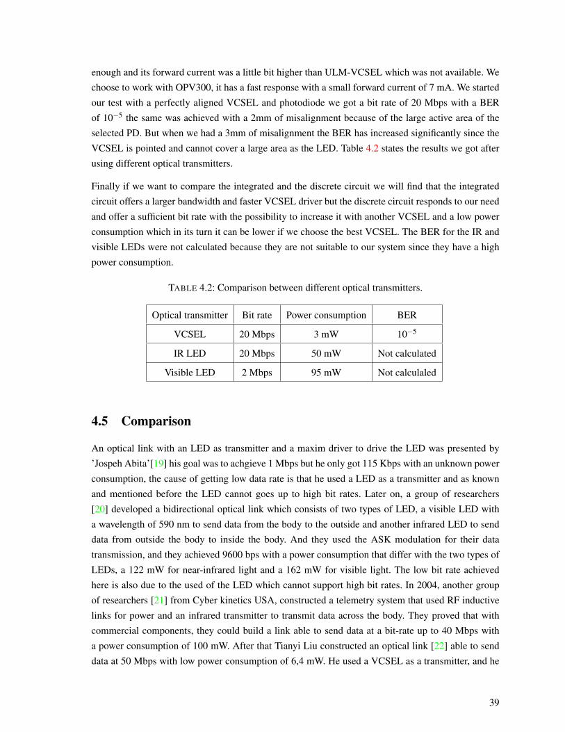
enough and its forward current was a little bit higher than ULM-VCSEL which was not available. We
choose to work with OPV300, it has a fast response with a small forward current of 7 mA. We started
our test with a perfectly aligned VCSEL and photodiode we got a bit rate of 20 Mbps with a BER
of 10−5 the same was achieved with a 2mm of misalignment because of the large active area of the
selected PD. But when we had a 3mm of misalignment the BER has increased significantly since the
VCSEL is pointed and cannot cover a large area as the LED. Table 4.2 states the results we got after
using different optical transmitters.
Finally if we want to compare the integrated and the discrete circuit we will find that the integrated
circuit offers a larger bandwidth and faster VCSEL driver but the discrete circuit responds to our need
and offer a sufficient bit rate with the possibility to increase it with another VCSEL and a low power
consumption which in its turn it can be lower if we choose the best VCSEL. The BER for the IR and
visible LEDs were not calculated because they are not suitable to our system since they have a high
power consumption.
TABLE 4.2: Comparison between different optical transmitters.
Optical transmitter Bit rate Power consumption BER
VCSEL 20 Mbps 3 mW 10−5
IR LED 20 Mbps 50 mW Not calculated
Visible LED 2 Mbps 95 mW Not calculaled
4.5 Comparison
An optical link with an LED as transmitter and a maxim driver to drive the LED was presented by
’Jospeh Abita’[19] his goal was to achgieve 1 Mbps but he only got 115 Kbps with an unknown power
consumption, the cause of getting low data rate is that he used a LED as a transmitter and as known
and mentioned before the LED cannot goes up to high bit rates. Later on, a group of researchers
[20] developed a bidirectional optical link which consists of two types of LED, a visible LED with
a wavelength of 590 nm to send data from the body to the outside and another infrared LED to send
data from outside the body to inside the body. And they used the ASK modulation for their data
transmission, and they achieved 9600 bps with a power consumption that differ with the two types of
LEDs, a 122 mW for near-infrared light and a 162 mW for visible light. The low bit rate achieved
here is also due to the used of the LED which cannot support high bit rates. In 2004, another group
of researchers [21] from Cyber kinetics USA, constructed a telemetry system that used RF inductive
links for power and an infrared transmitter to transmit data across the body. They proved that with
commercial components, they could build a link able to send data at a bit-rate up to 40 Mbps with
a power consumption of 100 mW. After that Tianyi Liu constructed an optical link [22] able to send
data at 50 Mbps with low power consumption of 6,4 mW. He used a VCSEL as a transmitter, and he
39
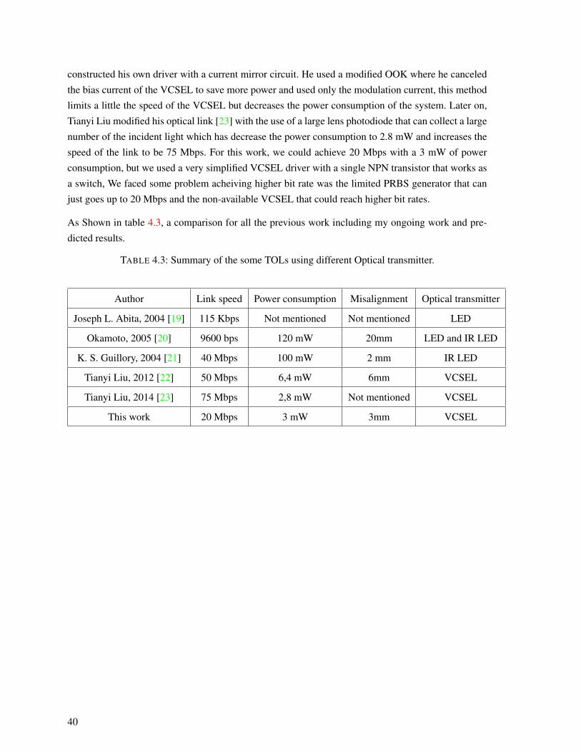
constructed his own driver with a current mirror circuit. He used a modified OOK where he canceled
the bias current of the VCSEL to save more power and used only the modulation current, this method
limits a little the speed of the VCSEL but decreases the power consumption of the system. Later on,
Tianyi Liu modified his optical link [23] with the use of a large lens photodiode that can collect a large
number of the incident light which has decrease the power consumption to 2.8 mW and increases the
speed of the link to be 75 Mbps. For this work, we could achieve 20 Mbps with a 3 mW of power
consumption, but we used a very simplified VCSEL driver with a single NPN transistor that works as
a switch, We faced some problem acheiving higher bit rate was the limited PRBS generator that can
just goes up to 20 Mbps and the non-available VCSEL that could reach higher bit rates.
As Shown in table 4.3, a comparison for all the previous work including my ongoing work and pre-
dicted results.
TABLE 4.3: Summary of the some TOLs using different Optical transmitter.
Author Link speed Power consumption Misalignment Optical transmitter
Joseph L. Abita, 2004 [19] 115 Kbps Not mentioned Not mentioned LED
Okamoto, 2005 [20] 9600 bps 120 mW 20mm LED and IR LED
K. S. Guillory, 2004 [21] 40 Mbps 100 mW 2 mm IR LED
Tianyi Liu, 2012 [22] 50 Mbps 6,4 mW 6mm VCSEL
Tianyi Liu, 2014 [23] 75 Mbps 2,8 mW Not mentioned VCSEL
This work 20 Mbps 3 mW 3mm VCSEL
40
Conclusion
In the past years, there has been great progress in implantable medical devices. A lot of diseases and
disabilities can be treated by implanting an electronic chip inside the human body ; these implanted
devices have greatly improved the life of patients. As for neural recording system, it helps for diag-
nosing brain diseases and gives a way to overcome these diseases, but this type of systems requires a
detailed study on how to record neural data and how to transmit the data to an external receiver. Our
focus was on the second part.
In chapter one, we listed all the specifications that our design has to respect. We found that the link
should be wireless in order not to damage the human tissue, so we compared different methods of data
transmission, and we choose to work with optical links due to several advantages. We did a detailed
study on the human skin which is the medium that will separate the transmitter and the receiver to
choose the best optical transmitter. We finally choose the VCSEL due to its speed and its wavelength
of 850 nm because at this wavelength, light propagates with less absorption and scattering comparing
to other wavelengths.
In chapter two, we did a literature review on some techniques used for wide-band wireless communi-
cation links through the skin, the data modulation used in those techniques and finally the Amplifier
used on the receiver side. We found that there is a bunch of researchers that are working on the sub-
ject with different methods of transmission, and they all have advantages and disadvantages. After a
group found the technique to use for the link, they will have to choose the way to encode data to make
compatible with the link, for that there are several ways, so we did a brief description on types of data
modulation used, and we compared them together. Finally, we reported some TIA designs that could
be used in our receiver side.
In chapter three, we designed an integrated Link Using 0.18 um CMOS Technology. This integrated
link consists of 2 parts, the transmitter side which is a VCSEL driver able to drive the VCSEL at high
bit rate with low power consumption and a receiver side that consists of a photodiode connected to a
CMOS transimpedance amplifier. This link shows better results, because when designing the discrete
link the VCSEL we were looking for was out of stock and this VCSEL has a higher bit rate with lower
power consumption.
In the last chapter,we designed a Discrete link with commercial components. We tried different optical
41
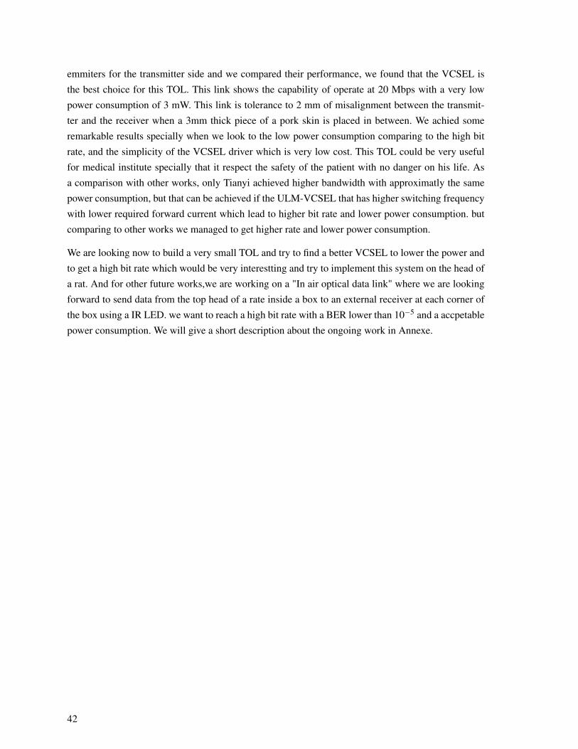
emmiters for the transmitter side and we compared their performance, we found that the VCSEL is
the best choice for this TOL. This link shows the capability of operate at 20 Mbps with a very low
power consumption of 3 mW. This link is tolerance to 2 mm of misalignment between the transmit-
ter and the receiver when a 3mm thick piece of a pork skin is placed in between. We achied some
remarkable results specially when we look to the low power consumption comparing to the high bit
rate, and the simplicity of the VCSEL driver which is very low cost. This TOL could be very useful
for medical institute specially that it respect the safety of the patient with no danger on his life. As
a comparison with other works, only Tianyi achieved higher bandwidth with approximatly the same
power consumption, but that can be achieved if the ULM-VCSEL that has higher switching frequency
with lower required forward current which lead to higher bit rate and lower power consumption. but
comparing to other works we managed to get higher rate and lower power consumption.
We are looking now to build a very small TOL and try to find a better VCSEL to lower the power and
to get a high bit rate which would be very interestting and try to implement this system on the head of
a rat. And for other future works,we are working on a "In air optical data link" where we are looking
forward to send data from the top head of a rate inside a box to an external receiver at each corner of
the box using a IR LED. we want to reach a high bit rate with a BER lower than 10−5 and a accpetable
power consumption. We will give a short description about the ongoing work in Annexe.
42
Annexe A
In Air Optical Link
In this chapter, we describe the ongoing work of a "In air optical data link" in which we tend to
build an optical link that would be able to send data in free space from a moving body to some fixed
photodetectors inside a small cage [59] using IR LED at a high bit rate of 20 Mbps with a low power
consumption less than 50 mW.
As shown in Figure we want to build the free air optical link in a small cage of 27x27 cm2, our
transmitter we be held on the head of a moving mouse and we will fix a large areas photodiode on
each top corner of the cage so we will make ensure that the transmitted signal will reach at least one of
the fixed photodetectors. This link has to be able to send data at 20 Mbps with a power consumption
of 40 mW.
FIGURE A.1: conceptual representation of the Optical link inside the cage
43
The LED driver is similar to the VCSEL driver we used before, we just changed the values of the
resistors so that the input current of the LED will be enough to turn it ON. Same thing for the receiver
side, the same receiver will be used due to its large bandwidth and the large area that covers. We had
the choice between 3 kinds of transmitters visible LED, IR LED and VCSEL. It is true that the VCSEL
will consume a lot less power than the IR LED but the problem with VCSEL since the Transmitter
will always be moving and the area covered with the VCSEL won’t be as big as the area covered with
an LED. But for LEDS even that the visible LEDs can cover large areas but its switching time is not
as fast as IR LED and it consumes more power. So we decided to choose IR LED because it meets our
specifications.
On the receiver side, we want to place a photodetector at each top corner of the cage, this photode-
tector will have the same amplification stage as before and we will use an adder for the 4 receiver to
have a clear signal because every photodetector will receive a small amount of the transmitted signal
depending on the direction of the mouse so we have to add all the received signals in order to have a
clear signal at the output. This is an ongoing work.
44
Bibliographie
[1] J. Savoj, B. Razavi, “High-Speed CMOS Circuits For Optical Receivers,” Kluer Acadamic Pu-
blishers.
[2] G.Mahdiraji and E. Zahedi, “Comparison Of Selected Digital Modulation Schemes (OOK, PPM
and DPIM) For Wireless Optical Communications,” 4th Student Conference On Research and
Development, June 2006.
[3] Encyclopaedia, “Human Skin.” htt p : //www.britannica.com/EBchecked/topic/547591/human−skin.
[4] Laserandhealthacademy, “Chromophores Absorption Coefficient.” htt p :
//www.laserandhealthacademy.com/en/public/lasers−medicine.
[5] C. R. Simpson, M. Kohl, M. Essenpreis, and M. Cope, “Near-infrared Optical Properties Of
Ex Vivo Human Skin And Subcutaneous Tissues Measured Using The Monte Carlo inversion
Technique,” Physics In Medicine And Biology, vol. 43, no. 9, p. 2465, 1998.
[6] A. Trabelsi, “Comparison Of Two CMOS Front-End Transimpedance Amplifiers for Optical
Biosensors,” IEEE Sensors Journal, vol. 13, February 2013.
[7] R. Normann, B. Greger, P. House, S. Romero, F. Pelayo, E. Fernandez, “Toward The Deve-
lopment Of A Cortically Based Visual Neuroprostheses,” Joural of Neural Engineering, vol. 6,
pp. 1–8, 2009.
[8] B. Gosselin, A. E. Ayoub, J.-F. Roy, M. Sawan, F. Lepore, A. Chaudhuri, and D. Guitton, “A
Mixed-Signal Multichip Neural Recording Interface With Bandwidth Reduction,” Biomedical
Circuits and Systems, IEEE Transactions on, vol. 3, no. 3, p. 129–141, 2009.
[9] H. McDermott, “An Advanced Multiple Channel Cochlear Implant,” IEEE Transactions On Bio-
medical Engineering, vol. 36, no. 7, pp. 789–797, 1989.
[10] M. Kiani, M. Ghovanloo, “An RFID-based Closed Loop Wireless Power Transmission System
For Biomedical Applications,” IEEE Transactions On Biomedical Circuits And Systems, vol. 57,
no. 4, pp. 260–264, 2010.
45

[11] S. Venkatraman, “In Vivo And In Vitro Evaluation Of PEDOT Microelectrodes For Neural Sti-
mulation And Recording,” IEEE Transactions On Neural Systems And Rehabilitation Enginee-
ring, vol. 19, no. 3, pp. 307–316, 2011.
[12] M. Yin, M. Ghovanloo, “Using Pulse Width Modulation For Wireless Transmission Of Neural
Signals In Multichannel Neural Recording Systems,” IEEE Transactions On Neural Systems And
Rehabilitation Engineering, vol. 17, no. 4, pp. 354–363, 2009.
[13] A. Sodagar, G. Perlin, Y. Yao, K. Najafi, K. Wise, “An Implantable 64-Channel Wireless Micro-
system for Single-Unit Neural Recording,” IEEE J Solid-State Circuits, vol. 44, no. 9, pp. 2591–
2604, 2009.
[14] M. Lebedev, M. Nicolelis, “Brain–Machine Interfaces : Past, Present and Future.,” Trends In
Neurosciences, vol. 29, no. 9, pp. 536–546, 2006.
[15] M. Yin, D. A. Borton, J. Aceros, W. R. Patterson and A. V. Nurmikko, “A 100-Channel Her-
metically Sealed Implantable Device for Chronic Wireless Neurosensing Applications,” IEEE
Transactions On Biomedical Circuits And Systems, vol. 7, pp. 115–128, April 2013.
[16] B. Gosselin, “Recent Advances in Neural Recording Microsystems,” Sensors, no. 11, pp. 4572–
7597, 2011.
[17] F. Shahrokhi, K. Abdelhalim, D. Serletis, P. Carlen, and R. Genov, “128-Channel Fully Diffe-
rential Digital Integrated Neural Recording And Stimulation Interface,” IEEE Transactions On
Biomedical Circuits And Systems, vol. 7, pp. 149–161, June 2010.
[18] M. Chae, W. T. Liu, Z. Yang, T.C. Chen, J. Kim, M. Sivaprakasam, and M. Yuce, “A 128-Channel
6mW Wireless Neural Recording IC with On-the-Fly Spike Sorting and UWB Transmitter,”
Solid-State Circuits Conference, vol. 7, pp. 146 – 603, 2008.
[19] J.L. Abita and W. Schneider, “Transdermal Optical Communications.,” .
[20] E. Okamoto, Y. Yamamoto, Y. Inoue, T. Makino, and Y. Mitamura, “Development Of A Bi-
directional Transcutaneous Optical Data Transmission System For Artificial Hearts Allowing
Long-Distance Data Communication With Low Electric Power Consumption,” The Japanese
Society For Articial Organs, vol. 8, no. 3, pp. 149–153, 2005.
[21] K. S. Guillory, A. K. Misener, A. Pungor, “Hybrid RF/IR Transcutaneous Telemetry For Power
And High-Bandwidth Data.,” Engineering in Medicine and Biology Society, vol. 2, pp. 4338–
4340, September 2004.
[22] T. Liu, U. Bihr, S. M. Anis and M. Ortmanns, “Optical Transcutaneous Link for Low Power,
High Data Rate Telemetry,” 34th Annual International Conference of the IEEE EMBS, pp. 3535
– 3538, 2012.
[23] T. Liu, U. Bihr, J. Anders and M. Ortmanns, “Performance Evaluation Of a Low Power Optical
Wireless Link For Biomedical Data Transfer,” Circuits and Systems (ISCAS), vol. 14, pp. 870–
873, June 2014.
46
[24] S. Shahdoost, B. Bozorgzade, A. Medi, N. Saniei, “Low Noise Transimpedance Amplifier
Design Procedure For Optical Communication,” Microelectronics (Austrochip), 22nd Austrian
Workshop, pp. 1–5, 2014.
[25] J. Lee, S. Jeong, S. B. Cho, S. M. Park, “TIA For Optical Communication,” Science And Tech-
nology, vol. 1, pp. 229–233, 2004.
[26] B. Nakhkoob, M.M. Hella, “A 5-Gb/s Noise Optimized Receiver Using a Switched TIA For Wi-
reless Optical Communications,” IEEE Transactions On Circuits And Systems, vol. 61, pp. 1255–
1268, April 2014.
[27] J. M. Kahn, J. R. Barry, “Wireless Infrared Communications.,” Proceedings of IEEE, vol. 85,
pp. 265–298, February 1997.
[28] J. Hamkins, “Pulse Position Modulation,” Data Transmission, and Digital and Optical Networks,
pp. 492–506, 2008.
[29] Y. Fujiwara, “Self-Synchronizing Pulse Position Modulation With Error Tolerance,” IEEE Tran-
sactions on Information Theory , vol. 59, pp. 5352–5362, 2013.
[30] K.T. Wong, “Narrowband PPM Semi-Blind Spatial-Rake Receiver and Co-Channel Interference
Suppression,” European Transactions on Telecommunications, vol. 18, pp. 193–197, 2007.
[31] Ghassemloy, Hayes, N.L. Seed and E.D. Kaluarachchi, “Digital Pulse Interval Modulation For
Optical Communication,” IEEE Communication Magazine , vol. 36, pp. 95–99, December 1998.
[32] U. Sethakaset and T. A. Gulliver, “Differential Amplitude Pulse-Position Modulation For Indoor
Wireless Optical Channels,” IEEE Global Telecommunications Conference, vol. 3, pp. 1867–
1871, December 2004.
[33] J. Zhang, “Modulation Analysis For Outdoors Applications Of Opticalwireless Communica-
tions,” IEEE Communication Technology Proceedings, vol. 2, pp. 1483–1487, August 2000.
[34] Laser Institute Of America, “American National Standard for Safe Use of Lasers.” htt ps :
//www.lia.org/PDF/Z1361s.pd f .
[35] H. Miranda, V. Gilja, C. A. Chestek, K. V. Shenoy and T. H. Meng, “A High-Rate Long-range
Wireless Transmission System for Simultaneous Multichannel Neural Recording Applications,”
IEEE Transactions on Biomedical Circuits and Systems, vol. 4, pp. 181–191, June 2010.
[36] B. Odom, “Ultrasound Analog Electronics Primer,” Analog Dialogue, vol. 5, p. 33, 1999.
[37] J. Jarvis, S. Salmons, “A family Of Neuromuscular Stimulators With Optical Transcutaneous
Control,” Journal of Medical Engineering and Technology, vol. 15, no. 2, pp. 53–57, 1991.
[38] Y. Mitamura, E. Okamoto, M. Tomohisa, “A transcutaneous Optical Information Transmission
System For Implantable Motor-driven Artificial Hearts,” ASAIO Transactions, vol. 36, pp. 278–
280, 1990.
47
[39] K. Goto, T. Nakagawa, “A 100-channel hermetically sealed implantable device for wireless
neurosensing applications,” IEEE Transsactions On Biomedical Circuits And Systems, vol. 7,
pp. 2629–2632, April 2013.
[40] K. Goto, T. Nakagawa, “Transcutaneous Photocoupler For Transmission Of Biological Signals,”
Optics Letters, vol. 27, no. 22, pp. 1797–1799, 2002.
[41] T. Vo-Dinh, Biomedical Photonics. CRC Press, 1998.
[42] T.L. Troy, S.N. Thennadil, “Optical Properties Of Human Skin In The Near-Infrared Wavelength
Range of 1000 To 2200 nm,” Biomedical Optics, vol. 6, no. 2, pp. 167–176, 2001.
[43] S.B. Alexander, “Optical Communication Receiver Design,” SPIE Optical Engineering Press,
1997.
[44] Krishnaswamy, G. Baranoski, “A Study On Skin Optics,” Technical Report, January 2004.
[45] T. Lister, P.A. Wright, P.H. Chappell, “Optical Properties Of Human Skin,” Journal Of Biomedi-
cal Optics, vol. 9, pp. 1–15, September 2012.
[46] R. R. Anderson and J. A. Parrish, “The optics Of Human Skin,” J. Invest.Dermatol., vol. 77,
no. 1, pp. 13–19, 1981.
[47] D. Zhu, K.V. Larin, Q. Luo and V.V. Tuchin, “Recent Progress In Tissue Optical Clearing,” Laser
Photonics, vol. 7, no. 5, p. 732–757, 2013.
[48] Y. He, R.K. Wang, “Dynamic Optical Clearing Effect Of Tissue Impregnated With Hyperosmos-
tic Agents And Studied With Optical Coherence Tomography,” Journal Of Biomedical Optics,
vol. 9, pp. 200–206, January 2004.
[49] Y. Ito, R.P. Kennan, E. Watanabe, H. Koizumi, “Assessment Of Heating Effects In Skin During
Continuous Near Infrared Spectroscopy,” Journal of Biomedical Optics, vol. 5, pp. 383–390,
October 2000.
[50] Bozkurt, B. Onaral, “Safety Assessment Of Near Infrared Light Emitting Diodes For Diffuse
Optical Measurements,” Biomedical Engineering Online, vol. 3, no. 9, 2004.
[51] B. Razavi, “Design Integrated Circuit For Optical Communication,” McGraW Hill, September
2012.
[52] T. C. Carusone, D. A. Johns, K. W. Martin, “Analog Integrated Circuit Design,” 2nd Edition,
2011.
[53] F.E. Kiamilev, A.V. Krishnamoorthy, “A High-Speed 32-Channel CMOS VCSEL Driver With
Built-In Self-Test And Clock Generation Circuitry,” Quantum Electronics, vol. 5, April 1999.
[54] OPTEK Technology, “Vertical Cavity Surface Emitting Laser.” htt p :
//optekinc.com/datasheets/OPV 300.pd f .
48
[55] California Eastern Laboratories, “NPN Silicon High Frequency Transistor.” htt p :
//www.cel.com/pd f/datasheets/ne856.pd f .
[56] ULM-Photonics, “Philips photonics.” htt p : //www.photonics.philips.com/.
[57] Hamamatsu, “S6967.” htt p : //www.hamamatsu.com/resources/pd f/ssd/s2506− 02− etc−kpin1048e.pd f .
[58] Texas Instruments, “Operational Amplifier.” htt p : //www.ti.com/lit/ds/symlink/opa842.pd f .
[59] S. A. Mirbozorgi, H. Bahrami, M. Sawan, and B. Gosselin, “A Smart Cage With Uniform Wire-
less Power Distribution in 3D for Enabling Long-Term Experiments With Freely Moving Ani-
mals,” EEE Transactions on Biomedical Circuits and Systems, 2015.
49