Embed Size (px)
Citation preview
Sun Microsystems, Inc. Fujitsu Limited901 San Antonio Road 4-1-1 KamikodanakaPalo Alto, CA 94303 Nahahara-ku, Kawasaki, 211-8588U.S.A. 650-960-1300 Japan
SPARC® Joint Programming Specification (JPS1): Commonality
Sun Microsystems and Fujitsu Limited
Release 1.0.4, 31 May 2002
Part No. 806-6753-1.0Release 1.0.4, 31 May 2002

PleaseRecycle
Copyright 2001 Sun Microsystems, Inc., 901 San Antonio Road, Palo Alto, California 94303 U.S.A. All rights reserved. Portions of this document are protected by copyright 1994 SPARC International, Inc.This product or document is protected by copyright and distributed under licenses restricting its use, copying, distribution, and decompilation. No part of this product or document may be reproduced in any form by any means without prior written authorization of Sun and its licensors, if any. Third-party software, including font technology, is copyrighted and licensed from Sun suppliers.Parts of the product may be derived from Berkeley BSD systems, licensed from the University of California. UNIX is a registered trademark in the U.S. and other countries, exclusively licensed through X/Open Company, Ltd.Sun, Sun Microsystems, the Sun logo, SunSoft, SunDocs, SunExpress, and Solaris are trademarks, registered trademarks, or service marks of Sun Microsystems, Inc. in the U.S. and other countries. All SPARC trademarks are used under license and are trademarks or registered trademarks of SPARC International, Inc. in the U.S. and other countries. Products bearing SPARC trademarks are based upon an architecture developed by Sun Microsystems, Inc. The OPEN LOOK and Sun™ Graphical User Interface was developed by Sun Microsystems, Inc. for its users and licensees. Sun acknowledges the pioneering efforts of Xerox in researching and developing the concept of visual or graphical user interfaces for the computer industry. Sun holds a non-exclusive license from Xerox to the Xerox Graphical User Interface, which license also covers Sun’s licensees who implement OPEN LOOK GUIs and otherwise comply with Sun’s written license agreements.RESTRICTED RIGHTS: Use, duplication, or disclosure by the U.S. Government is subject to restrictions of FAR 52.227-14(g)(2)(6/87) and FAR 52.227-19(6/87), or DFAR 252.227-7015(b)(6/95) and DFAR 227.7202-3(a).
DOCUMENTATION IS PROVIDED “AS IS” AND ALL EXPRESS OR IMPLIED CONDITIONS, REPRESENTATIONS AND WARRANTIES, INCLUDING ANY IMPLIED WARRANTY OF MERCHANTABILITY, FITNESS FOR A PARTICULAR PURPOSE OR NON-INFRINGEMENT, ARE DISCLAIMED, EXCEPT TO THE EXTENT THAT SUCH DISCLAIMERS ARE HELD TO BE LEGALLY INVALID.
Copyright 2001 Sun Microsystems, Inc., 901 San Antonio Road • Palo Alto, CA 94303-4900 Etats-Unis. Tous droits réservés. Ce produit ou document est protégé par un copyright et distribué avec des licences qui en restreignent l’utilisation, la copie, la distribution, et la décompilation. Aucune partie de ce produit ou document ne peut être reproduite sous aucune forme, par quelque moyen que ce soit, sans l’autorisation préalable et écrite de Sun et de ses bailleurs de licence, s’il y en a. Le logiciel détenu par des tiers, et qui comprend la technologie relative aux polices de caractères, est protégé par un copyright et licencié par des fournisseurs de Sun.Des parties de ce produit pourront être dérivées des systèmes Berkeley BSD licenciés par l’Université de Californie. UNIX est une marque déposée aux Etats-Unis et dans d’autres pays et licenciée exclusivement par X/Open Company, Ltd. La notice suivante est applicable à Netscape Communicator™: Copyright 1995 Netscape Communications Corporation. Tous droits réservés. Sun, Sun Microsystems, the Sun logo, AnswerBook2, docs.sun.com, et Solaris sont des marques de fabrique ou des marques déposées, ou marques de service, de Sun Microsystems, Inc. aux Etats-Unis et dans d’autres pays. Toutes les marques SPARC sont utilisées sous licence et sont des marques de fabrique ou des marques déposées de SPARC International, Inc. aux Etats-Unis et dans d’autres pays. Les produits portant les marques SPARC sont basés sur une architecture développée par Sun Microsystems, Inc.L’interface d’utilisation graphique OPEN LOOK et Sun™ a été développée par Sun Microsystems, Inc. pour ses utilisateurs et licenciés. Sun reconnaît les efforts de pionniers de Xerox pour la recherche et le développement du concept des interfaces d’utilisation visuelle ou graphique pour l’industrie de l’informatique. Sun détient une licence non exclusive de Xerox sur l’interface d’utilisation graphique Xerox, cette licence couvrant également les licenciés de Sun qui mettent en place l’interface d’utilisation graphique OPEN LOOK et qui en outre se conforment aux licences écrites de Sun.
CETTE PUBLICATION EST FOURNIE "EN L’ETAT" ET AUCUNE GARANTIE, EXPRESSE OU IMPLICITE, N’EST ACCORDEE, Y COMPRIS DES GARANTIES CONCERNANT LA VALEUR MARCHANDE, L’APTITUDE DE LA PUBLICATION A REPONDRE A UNE UTILISATION PARTICULIERE, OU LE FAIT QU’ELLE NE SOIT PAS CONTREFAISANTE DE PRODUIT DE TIERS. CE DENI DE GARANTIE NE S’APPLIQUERAIT PAS, DANS LA MESURE OU IL SERAIT TENU JURIDIQUEMENT NUL ET NON AVENU.
Copyright© 2001 Fujitsu Limited, 4-1-1 Kamikodanaka, Nahahara-ku, Kawasaki, 211-8588, Japan. All rights reserved.This product and related documentation are protected by copyright and distributed under licenses restricting their use, copying, distribution, and decompilation. No part of this product or related documentation may be reproduced in any form by any means without prior written authorization of Fujitsu Limited and HAL Computer Systems, Inc., and its licensors, if any.Portions of this product may be derived from the UNIX and Berkeley 4.3 BSD Systems, licensed from UNIX System Laboratories, Inc., a wholly owned subsidiary of Novell, Inc., and the University of California, respectively.The product described in this book may be protected by one or more U.S. patents, foreign patents, or pending applications.TRADEMARKSHAL and the HAL logo are registered trademarks of HAL Computer Systems, Inc. SPARC64® is a registered trademark of SPARC International, Inc., licensed exclusively to Fujitsu Limited and HAL Computer Systems, Inc.Fujitsu and the Fujitsu logo are trademarks of Fujitsu Limited.This publication is provided “as is” without warranty of any kind, either express or implied, including, but not limited to, the implied warranties of merchantability, fitness for a particular purpose, or noninfringement.This publication could include technical inaccuracies or typographical errors. changes are periodically added to the information herein; these changes will be incorporated in new editions of the publication. hal computer systems, inc. may make improvements and/or changes in the product(s) and/or the program(s) described in this publication at any time.Sun Microsystems, Inc. Fujitsu Limited901 San Antonio 4-1-1 KamikodanakaPalo Alto, California, 94303 Nahahara-ku, Kawasaki, 211-8588U.S.A. Japanhttp://www.sun.com http://www.fujitsu.com/
Contents
Preface xv
1. Overview 1
1.1 Navigating the SPARC Joint Programming Specification 2
1.2 Fonts and Notational Conventions 31.2.1 Implementation Dependencies 41.2.2 Notation for Numbers 41.2.3 Informational Notes 4
1.3 SPARC V9 Architecture 51.3.1 Features 51.3.2 Attributes 61.3.3 System Components 61.3.4 Architectural Definition 71.3.5 SPARC V9 Compliance 8
2. Definitions 9
3. Architectural Overview 19
3.1 SPARC V9 Processor Architecture 193.1.1 Integer Unit (IU) 203.1.2 Floating-Point Unit (FPU) 20
3.2 Instructions 203.2.1 Memory Access 213.2.2 Arithmetic / Logical / Shift Instructions 23
Contents i
3.2.3 Control Transfer 233.2.4 State Register Access 243.2.5 Floating-Point Operate 243.2.6 Conditional Move 253.2.7 Register Window Management 25
3.3 Traps 25
4. Data Formats 27
4.1 Signed, Unsigned, and Tagged Integer Data Formats 284.1.1 Signed Integer Data Types 294.1.2 Unsigned Integer Data Types 314.1.3 Tagged Word 32
4.2 Floating-Point Data Types 324.2.1 Floating Point, Single Precision 334.2.2 Floating Point, Double Precision 334.2.3 Floating Point, Quad Precision 344.2.4 Floating-Point Data Alignment in Memory and Registers 35
4.3 Graphics Data Formats 364.3.1 Pixel Graphics Format 364.3.2 Fixed16 Graphics Format 364.3.3 Fixed32 Graphics Format 37
5. Registers 39
5.1 Nonprivileged Registers 405.1.1 General-Purpose r Registers 405.1.2 Special r Registers 465.1.3 IU Control/Status Registers 465.1.4 Floating-Point Registers 485.1.5 Integer Condition Codes Register (CCR) 545.1.6 Floating-Point Registers State (FPRS) Register 555.1.7 Floating-Point State Register (FSR) 565.1.8 Address Space Identifier (ASI) Register 675.1.9 Tick (TICK) Register 68
5.2 Privileged Registers 695.2.1 Processor State (PSTATE) Register 69
ii SPARC® Joint Programming Specification (JPS1): Commonality • Release 1.0.4, 31 May 2002
5.2.2 Trap Level Register (TL) 745.2.3 Processor Interrupt Level (PIL) Register 755.2.4 Trap Program Counter (TPC) Registers 755.2.5 Trap Next Program Counter (TNPC) Registers 765.2.6 Trap State (TSTATE) Registers 775.2.7 Trap Type (TT) Registers 775.2.8 Trap Base Address (TBA) Register 785.2.9 Version (VER) Register 795.2.10 Register-Window State Registers 805.2.11 Ancillary State Registers (ASRs) 835.2.12 Registers Referenced Through ASIs 915.2.13 Floating-Point Deferred-Trap Queue (FQ) 985.2.14 Integer Unit Deferred-Trap Queue 99
6. Instructions 101
6.1 Instruction Execution 101
6.2 Instruction Formats and Fields 102
6.3 Instruction Categories 1066.3.1 Memory Access Instructions 1076.3.2 Integer Arithmetic Instructions 1136.3.3 Control-Transfer Instructions (CTIs) 1146.3.4 Register Window Management Instructions 1206.3.5 State Register Access 1226.3.6 Privileged Register Access 1236.3.7 Floating-Point Operate (FPop) Instructions 1236.3.8 Implementation-Dependent Instructions 1246.3.9 Reserved Opcodes and Instruction Fields 1256.3.10 Summary of Unimplemented Instructions 125
6.4 Register Window Management 1266.4.1 Register Window State Definition 1266.4.2 Register Window Traps 127
7. Traps 131
7.1 Processor States, Normal and Special Traps 1327.1.1 RED_state 1337.1.2 Error_state 136
Release 1.0.4, 31 May 2002 Contents iii
7.2 Trap Categories 1377.2.1 Precise Traps 1377.2.2 Deferred Traps 1377.2.3 Disrupting Traps 1387.2.4 Reset Traps 1397.2.5 Uses of the Trap Categories 139
7.3 Trap Control 1407.3.1 PIL Control 1417.3.2 TEM Control 141
7.4 Trap-Table Entry Addresses 1417.4.1 Trap Table Organization 1427.4.2 Trap Type (TT) 1427.4.3 Trap Priorities 1477.4.4 Details of Supported Traps 148
7.5 Trap Processing 1497.5.1 Normal Trap Processing 1517.5.2 Fast MMU Trap Processing 1527.5.3 Interrupt Vector Trap Processing 1547.5.4 Special Trap Processing 155
7.6 Exception and Interrupt Descriptions 1617.6.1 Traps Defined by SPARC V9 As Mandatory 1627.6.2 SPARC V9 Optional Traps That Are Mandatory in SPARC JPS1
1657.6.3 SPARC V9 Optional Traps That Are Optional in SPARC JPS1 1667.6.4 SPARC V9 Implementation-Dependent, Optional Traps That Are
Mandatory in SPARC JPS1 1677.6.5 SPARC JPS1 Implementation-Dependent Traps 167
8. Memory Models 169
8.1 Overview 170
8.2 Memory, Real Memory, and I/O Locations 171
8.3 Addressing and Alternate Address Spaces 173
8.4 SPARC V9 Memory Model 1758.4.1 SPARC V9 Program Execution Model 1758.4.2 Processor/Memory Interface Model 177
iv SPARC® Joint Programming Specification (JPS1): Commonality • Release 1.0.4, 31 May 2002
8.4.3 MEMBAR Instruction 1798.4.4 Memory Models 1818.4.5 Mode Control 1828.4.6 Hardware Primitives for Mutual Exclusion 1828.4.7 Synchronizing Instruction and Data Memory 183
A. Instruction Definitions 185
A.1 Add 192A.2 Alignment Instructions (VIS I) 194A.3 Three-Dimensional Array Addressing Instructions (VIS I) 196A.4 Block Load and Store (VIS I) 199A.5 Byte Mask and Shuffle Instructions (VIS II) 203A.6 Branch on Integer Register with Prediction (BPr) 205A.7 Branch on Floating-Point Condition Codes with Prediction (FBPfcc) 207A.8 Branch on Integer Condition Codes with Prediction (BPcc) 210A.9 Call and Link 213A.10 Compare and Swap 214A.11 DONE and RETRY 217A.12 Edge Handling Instructions (VIS I, II) 218A.13 Floating-Point Add and Subtract 221A.14 Floating-Point Compare 223A.15 Convert Floating-Point to Integer 225A.16 Convert Between Floating-Point Formats 227A.17 Convert Integer to Floating-Point 229A.18 Floating-Point Move 231A.19 Floating-Point Multiply and Divide 233A.20 Floating-Point Square Root 235A.21 Flush Instruction Memory 236A.22 Flush Register Windows 238A.23 Illegal Instruction Trap 239A.24 Implementation-Dependent Instructions 240A.25 Jump and Link 241A.26 Load Floating-Point 242A.27 Load Floating-Point from Alternate Space 244A.28 Load Integer 247A.29 Load Integer from Alternate Space 249
Release 1.0.4, 31 May 2002 Contents v
A.30 Load Quadword, Atomic (VIS I) 251A.31 Load-Store Unsigned Byte 253A.32 Load-Store Unsigned Byte to Alternate Space 254A.33 Logical Operate Instructions (VIS I) 256A.34 Logical Operations 259A.35 Memory Barrier 261A.36 Move Floating-Point Register on Condition (FMOVcc) 264A.37 Move Floating-Point Register on Integer Register Condition (FMOVr) 270A.38 Move Integer Register on Condition (MOVcc) 272A.39 Move Integer Register on Register Condition (MOVr) 277A.40 Multiply and Divide (64-bit) 279A.41 No Operation 281A.42 Partial Store (VIS I) 282A.43 Partitioned Add/Subtract Instructions (VIS I) 284A.44 Partitioned Multiply Instructions (VIS I) 286
A.44.1 FMUL8x16 Instruction 287A.44.2 FMUL8x16AU Instruction 288A.44.3 FMUL8x16AL Instruction 288A.44.4 FMUL8SUx16 Instruction 289A.44.5 FMUL8ULx16 Instruction 289A.44.6 FMULD8SUx16 Instruction 290A.44.7 FMULD8ULx16 Instruction 291
A.45 Pixel Compare (VIS I) 292A.46 Pixel Component Distance (PDIST) (VIS I) 294A.47 Pixel Formatting (VIS I) 295
A.47.1 FPACK16 296A.47.2 FPACK32 297A.47.3 FPACKFIX 298A.47.4 FEXPAND 299A.47.5 FPMERGE 300
A.48 Population Count 301A.49 Prefetch Data 303
A.49.1 SPARC V9 Prefetch Variants 305A.49.2 SPARC JPS1 Prefetch Variants (fcn = 20–23) 307A.49.3 Implementation-Dependent Prefetch Variants (fcn = 16–19, 24–
31) 308
vi SPARC® Joint Programming Specification (JPS1): Commonality • Release 1.0.4, 31 May 2002
A.49.4 General Comments 309A.50 Read Privileged Register 311A.51 Read State Register 313A.52 RETURN 316A.53 SAVE and RESTORE 318A.54 SAVED and RESTORED 321A.55 Set Interval Arithmetic Mode (VIS II) 322A.56 SETHI 323A.57 Shift 324A.58 Short Floating-Point Load and Store
(VIS I) 326A.59 SHUTDOWN (VIS I) 328A.60 Software-Initiated Reset 329A.61 Store Floating-Point 330A.62 Store Floating-Point into Alternate Space 333A.63 Store Integer 336A.64 Store Integer into Alternate Space 338A.65 Subtract 340A.66 Tagged Add 342A.67 Tagged Subtract 343A.68 Trap on Integer Condition Codes (Tcc) 344A.69 Write Privileged Register 347A.70 Write State Register 350A.71 Deprecated Instructions 353
A.71.1 Branch on Floating-Point Condition Codes (FBfcc) 355A.71.2 Branch on Integer Condition Codes (Bicc) 358A.71.3 Divide (64-bit / 32-bit) 361A.71.4 Load Floating-Point Status Register 364A.71.5 Load Integer Doubleword 365A.71.6 Load Integer Doubleword from Alternate Space 367A.71.7 Multiply (32-bit) 369A.71.8 Multiply Step 371A.71.9 Read Y Register 373A.71.10 Store Barrier 374A.71.11 Store Floating-Point Status Register Lower 375A.71.12 Store Integer Doubleword 377
Release 1.0.4, 31 May 2002 Contents vii
A.71.13 Store Integer Doubleword into Alternate Space 379A.71.14 Swap Register with Memory 381A.71.15 Swap Register with Alternate Space Memory 383A.71.16 Tagged Add and Trap on Overflow 385A.71.17 Tagged Subtract and Trap on Overflow 387A.71.18 Write Y Register 389
B. IEEE Std 754-1985 Requirements for SPARC V9 391
B.1 Traps Inhibiting Results 392B.2 NaN Operand and Result Definitions 392
B.2.1 Untrapped Result in Different Format from Operands 393B.2.2 Untrapped Result in Same Format as Operands 393
B.3 Trapped Underflow Definition (UFM = 1) 394B.4 Untrapped Underflow Definition (UFM = 0) 395B.5 Integer Overflow Definition 396B.6 Floating-Point Nonstandard Mode 396
C. Implementation Dependencies 397
C.1 Definition of an Implementation Dependency 398C.2 Hardware Characteristics 398C.3 Implementation Dependency Categories 399C.4 List of Implementation Dependencies 399
D. Formal Specification of the Memory Models 413
D.1 Processors and Memory 413D.2 Overview of the Memory Model Specification 414D.3 Memory Transactions 415
D.3.1 Memory Transactions 415D.3.2 Program Order 416D.3.3 Dependence Order 417D.3.4 Memory Order 418
D.4 Specification of Relaxed Memory Order (RMO) 418D.4.1 Value Atomicity 418D.4.2 Store Atomicity 419D.4.3 Atomic Memory Transactions 419D.4.4 Memory Order Constraints 419
viii SPARC® Joint Programming Specification (JPS1): Commonality • Release 1.0.4, 31 May 2002
D.4.5 Value of Memory Transactions 419D.4.6 Termination of Memory Transactions 420D.4.7 Flush Memory Transaction 420
D.5 Specification of Partial Store Order (PSO) 420D.6 Specification of Total Store Order (TSO) 420D.7 Examples of Program Executions 421
D.7.1 Observation of Store Atomicity 421D.7.2 Dekker’s Algorithm 423D.7.3 Indirection Through Processors 424D.7.4 PSO Behavior 425D.7.5 Application to Compilers 426D.7.6 Verifying Memory Models 426
E. Opcode Maps 427
F. Memory Management Unit 437
F.1 Virtual Address Translation 437F.2 Translation Table Entry (TTE) 440F.3 Translation Storage Buffer 443
F.3.1 TSB Indexing Support 443F.3.2 TSB Cacheability 444F.3.3 TSB Organization 444
F.4 Hardware Support for TSB Access 445F.4.1 Typical TLB Miss/Refill Sequence 445F.4.2 TSB Pointer Formation 445F.4.3 Required TLB Conditions 448F.4.4 Required TSB Conditions 448F.4.5 MMU Global Registers Selection 448
F.5 Faults and Traps 449F.6 MMU Operation Summary 451F.7 ASI Value, Context, and Endianness Selection for Translation 453F.8 Reset, Disable, and RED_state Behavior 455F.9 SPARC V9 “MMU Requirements” Annex 457F.10 Internal Registers and ASI Operations 457
F.10.1 Accessing MMU Registers 458F.10.2 Context Registers 459F.10.3 Instruction/Data MMU TLB Tag Access Registers 460
Release 1.0.4, 31 May 2002 Contents ix
F.10.4 I/D TLB Data In, Data Access, and Tag Read Registers 461F.10.5 I/D TSB Tag Target Registers 464F.10.6 I/D TSB Base Registers 464F.10.7 I/D TSB Extension Registers 466F.10.8 I/D TSB 8-Kbyte and 64-Kbyte Pointer and Direct Pointer
Registers 466F.10.9 I/D Synchronous Fault Status Registers (I-SFSR, D-SFSR) 467F.10.10 Synchronous Fault Addresses 469F.10.11 I/D MMU Demap 470
F.11 MMU Bypass 472F.12 Translation Lookaside Buffer Hardware 473
F.12.1 TLB Operations 473F.12.2 TLB Replacement Policy 473F.12.3 TSB Pointer Logic Hardware Description 474
G. Assembly Language Syntax 475
G.1 Notation Used 475G.1.1 Register Names 476G.1.2 Special Symbol Names 477G.1.3 Values 480G.1.4 Labels 481G.1.5 Other Operand Syntax 481G.1.6 Comments 483
G.2 Syntax Design 483G.3 Synthetic Instructions 484
H. Software Considerations 487
H.1 Nonprivileged Software 487H.1.1 Registers 487H.1.2 Leaf-Procedure Optimization 491H.1.3 Example Code for a Procedure Call 493H.1.4 Register Allocation Within a Window 494H.1.5 Other Register-Window-Usage Models 494H.1.6 Self-Modifying Code 495H.1.7 Thread Management 495H.1.8 Minimizing Branch Latency 496
x SPARC® Joint Programming Specification (JPS1): Commonality • Release 1.0.4, 31 May 2002
H.1.9 Prefetch 497H.1.10 Nonfaulting Load 500
H.2 Supervisor Software 503H.2.1 Trap Handling 503H.2.2 Example Code for Spill Handler 504H.2.3 Client-Server Model 504H.2.4 User Trap Handlers 505
I. Extending the SPARC V9 Architecture 509
I.1 Read/Write Ancillary State Registers (ASRs) 509I.2 Implementation-Dependent and Reserved Opcodes 510
J. Programming with the Memory Models 511
J.1 Memory Operations 512J.2 Memory Model Selection 512J.3 Processors and Processes 513J.4 Higher-Level Programming Languages and Memory Models 513J.5 Portability and Recommended Programming Style 514J.6 Spin Locks 516J.7 Producer-Consumer Relationship 517J.8 Process Switch Sequence 519J.9 Dekker’s Algorithm 520J.10 Code Patching 521J.11 Fetch_and_Add 523J.12 Barrier Synchronization 524J.13 Linked List Insertion and Deletion 525J.14 Communicating with I/O Devices 526
J.14.1 I/O Registers with Side Effects 527J.14.2 The Control and Status Register (CSR) 528J.14.3 The Descriptor 529J.14.4 Lock-Controlled Access to a Device Register 529
K. Changes from SPARC V8 to SPARC V9 531
K.1 Trap Model 531K.2 Data Formats 532K.3 Little-Endian Support 532
Release 1.0.4, 31 May 2002 Contents xi
K.4 Little-Endian Byte Order 532K.5 Registers 532K.6 Alternate Space Access 534K.7 Instruction Set 534K.8 Memory Model 536
L. Address Space Identifiers 537
L.1 Address Space Identifiers and Address Spaces 537L.2 ASI Values 538L.3 ASI Assignments 538
L.3.1 Supported ASIs 538L.3.2 Special Memory Access ASIs 546
M. Caches and Cache Coherency 551
N. Interrupt Handling 553
N.1 Interrupt Vector Dispatch 554N.2 Interrupt Vector Receive 555N.3 Interrupt Global Registers 556N.4 Interrupt ASI Registers 556
N.4.1 Outgoing Interrupt Vector Data<7:0> Register 556N.4.2 Interrupt Vector Dispatch Register 557N.4.3 Interrupt Vector Dispatch Status Register 558N.4.4 Incoming Interrupt Vector Data<7:0> 558N.4.5 Interrupt Vector Receive Register 559
N.5 Software Interrupt Register (SOFTINT) 560N.5.1 Setting the Software Interrupt Register 560N.5.2 Clearing the Software Interrupt Register 561
O. Reset, RED_state, and Error_state 563
O.1 RED_state Characteristics 563O.2 Resets 564
O.2.1 Externally Initiated Reset (XIR) 564O.2.2 error_state and Watchdog Reset (WDR) 565O.2.3 Software-Initiated Reset (SIR) 565
O.3 RED_state Trap Vector 565O.4 Machine States 565
xii SPARC® Joint Programming Specification (JPS1): Commonality • Release 1.0.4, 31 May 2002
P. Error Handling 569
P.1 Error Classes and Signalling 570P.1.1 Error Classes in Severity 570P.1.2 Errors Asynchronous to Instruction Execution 570
P.2 Corrective Actions 571P.2.1 Reset-Inducing ERROR Signal 573P.2.2 Precise Traps 574P.2.3 Deferred Traps 574P.2.4 Disrupting Traps 577
P.3 Related Traps 578P.4 Related Registers/Error Logging 579P.5 Signalling/Special ECC 580
Q. Performance Instrumentation 581
Bibliography 583
Release 1.0.4, 31 May 2002 Contents xiii

xiv SPARC® Joint Programming Specification (JPS1): Commonality • Release 1.0.4, 31 May 2002
Preface
SPARC® V9 is the standard instruction set architecture developed by SPARC International for 64-bit SPARC processors. Although the standard serves the needs of application programmers, some processor functions that primarily affect system programmers are left uncovered or implementation dependent in the standard. Sun Microsystems, with its UltraSPARC® III implementation, and Fujitsu, with its SPARC64® V implementation, jointly worked to increase the commonalities between their processors in the areas that SPARC V9 does not cover. Both companies intend to continue this collaborative effort for future processor generations.
The SPARC Joint Programming Specification is based on SPARC V9. It first defines the programmer's model and the hardware behavior common to the processors from both companies. These aspects of the processors conform to the instruction set architecture, memory model, error and trap handling specified by The SPARC Architecture Manual-Version 9 and also conform to additional feature conventions jointly established by Sun and Fujitsu. Some features, especially initialization, error detection, error recovery, etc., strongly depend on the specific implementation and cannot be common. Such features and specific implementation-dependent deviations from common definitions are detailed in Implementation Supplements that are companions to this document.
Who Should Use This BookProgrammers who write code for the UltraSPARC III processor, the SPARC64 V processor, and the successors of both processor lines will find this book, combined with Implementation Supplements, the single depository of information that logic designers, operating system programmers, or application software programmers can share to gain a common understanding of the features of SPARC processors from both Sun Microsystems, Inc., and Fujitsu.
Release 1.0.4, 31 May 2002 Preface xv
How This Book Is OrganizedThe book is organized in major sections: Commonality, which contains information that is common to all implementations, and Implementation Supplements. At present, we describe two implementations: SPARC64 V, the Fujitsu implementation of SPARC V9, and UltraSPARC III, the Sun Microsystems implementation. Other implementations may be added in the future.
The Commonality section and the Implementation Supplements begin at Chapter 1, page 1, each supplement contains its own index, and all supplements in general follow the organization of the The SPARC Architecture Manual-Version 9, as follows.
Chapter 1, Overview, describes features, attributes, and components and provides a high-level view of SPARC V9 and the implementations.
Chapter 2, Definitions, defines terms you should know before reading the book or parts.
Chapter 3, Architectural Overview, describes processors and instructions.
Chapter 4, Data Formats, presents data types.
Chapter 5, Registers, discusses the two types of registers: general-purpose (working data) registers and control/status registers.
Chapter 6, Instructions, details nuts and bolts of instructions.
Chapter 7, Traps, describes types, behavior, control, and processing of traps.
Chapter 8, Memory Models, discusses three types of memory models: Total Store Order, Partial Store Order, and Relaxed Memory Order.
An extensive set of appendixes complements the chapters. Appendixes D, H, I, J, and K contain material from The SPARC Architecture Manual-Version 9.
Appendix A, Instruction DefinitionsAppendix B, IEEE Std 754-1985 Requirements for SPARC V9Appendix C, Implementation DependenciesAppendix D, Formal Specification of the Memory ModelsAppendix E, Opcode MapsAppendix F, Memory Management UnitAppendix G, Assembly Language SyntaxAppendix H, Software Considerations (Informative)Appendix I, Extending the SPARC V9 Architecture (Informative)Appendix J, Programming with the Memory Models (Informative)Appendix K, Changes from SPARC V8 to SPARC V9Appendix L, Address Space Identifiers
xvi SPARC® Joint Programming Specification (JPS1): Commonality • Release 1.0.4, 31 May 2002
Appendix N, Interrupt HandlingAppendix O, Reset, RED_state, and Error_stateAppendix P, Error Handling
The Implementation Supplements to the book contain additional appendixes on implementation-specific topics such as cache organization, performance instrumentation, and interconnect programming model.
For navigation suggestions, see Chapter 1, Overview.
Editorial ConventionsFor editorial conventions, see Chapter 1, Overview. Notational conventions of SPARC Joint Programming Specification generally follow those of The SPARC Architecture Manual-Version 9 and differ slightly from the standard Sun Microsystems notational conventions.
Related ReadingThe SPARC Joint Programming Specification refers to these related books:
■ The SPARC Architecture Manual-Version 9■ UltraSPARC™ User’s Manual■ Implementation Characteristics of Current SPARC-V9-based Products, Revision 9.x
(SPARC International)■ SPARC64™ Processor User’s Guide
See also the bibliography section of Commonality and Implementations.
Release 1.0.4, 31 May 2002 Preface xvii

xviii SPARC® Joint Programming Specification (JPS1): Commonality • Release 1.0.4, 31 May 2002
C.CHAPTER 1
Overview
The SPARC Joint Programming Specification (SPARC JPS1) specifies a particular subset of SPARC V9 implementations, including Fujitsu’s SPARC64 V, Sun Microsystem’s UltraSPARC III, and certain successors to those processors.
SPARC JPS1 was derived directly from the source text of The SPARC Architecture Manual-Version 9. Some theoretical material contained in The SPARC Architecture Manual-Version 9 has been omitted, but for some implementors, this theoretical information is important. In particular, operating system programmers who write memory management software, compiler writers who write machine-specific optimizers, and anyone who writes code to run on all SPARC V9-compatible machines should obtain and use The SPARC Architecture Manual-Version 9. Readers of SPARC Joint Programming Specification could profit from using The SPARC Architecture Manual-Version 9 as a companion text.
Software that is intended to be portable across all SPARC V9 processors should adhere to The SPARC Architecture Manual-Version 9.
Material in this document identified as relevant to SPARC JPS1 (or just “JPS1”) processors may not apply to other SPARC V9 processors. Therefore, in Appendixes D, H, I, J, and K, we duplicated the information contained in the same appendixes of The SPARC Architecture Manual-Version 9. Because we have added and deleted a significant number of tables and figures, the table and figure numbers in this guide are not parallel with the numbers in The SPARC Architecture Manual-Version 9.
In this book, the word architecture refers to the machine details that are visible to an assembly language programmer or to the compiler code generator. It does not include details of the implementation that are not visible or easily observable by software.
In this chapter, we discuss:
■ Navigating the SPARC Joint Programming Specification on page 2■ Fonts and Notational Conventions on page 3■ SPARC V9 Architecture on page 5
Release 1.0.4, 31 May 2002 C. Chapter 1 • Overview 1
1.1 Navigating the SPARC Joint Programming SpecificationIf you are new to SPARC, read Chapter 3, Architectural Overview, study the definitions in Chapter 2, Definitions, then look into the subsequent s and appendixes for more details in areas of interest to you.
If you are familiar with SPARC V8 but not SPARC V9, you should review the list of changes in Appendix K. For additional details of architectural changes, review the following s:
■ Chapter 4, Data Formats, for a description of the supported data formats
■ Chapter 5, Registers, for a description of the register set
■ Chapter 6, Instructions, for a description of the new instructions
■ Chapter 7, Traps, for a description of the trap model
■ Chapter 8, Memory Models, for a description of the memory models
■ Appendix A, Instruction Definitions, for descriptions of the instructions
Finally, if you are familiar with the SPARC V9 architecture and want to familiarize yourself with the Sun- and Fujitsu-specific implementations, study the following chapters and appendices in the Sun- and Fujitsu-specific Implementation Supplements:
■ Chapter 2, Definitions
■ Appendix A, Instruction Definitions, for descriptions of specific instruction extensions
■ Appendix C, Implementation Dependencies, for descriptions of resolutions of all SPARC V9 implementation dependencies
■ Appendix E, Opcode Maps, to see how opcode extensions fit into the SPARC V9 opcode maps
■ Appendix F, Memory Management Unit, to see the common features of the SPARC JPS1 Memory Management Unit and the implementation-specific features of that MMU.
■ Appendix G, Assembly Language Syntax, to see extensions to the SPARC V9 assembly language syntax; in particular, synthetic instructions are documented in this appendix
2 SPARC® Joint Programming Specification (JPS1): Commonality • Release 1.0.4, 31 May 2002
1.2 Fonts and Notational ConventionsFonts are used as follows:
■ Italic font is used for emphasis, book titles, and the first instance of a word that is defined.
■ Italic font is also used for assembly language terms.
■ Italic sans serif font is used for exception and trap names. For example, “The privileged_action exception....”
■ Typewriter font (Courier) is used for register fields (named bits), instruction fields, and read-only register fields. For example: “The rs1 field contains....”
■ Typewriter font is used for literals, instruction names, register names, and software examples.
■ UPPERCASE items are acronyms, instruction names, or writable register fields. Some common acronyms appear in the glossary in Chapter 2, Definitions. Note: Names of some instructions contain both upper- and lowercase letters.
■ Underbar characters join words in register, register field, exception, and trap names. Note: Such words can be split across lines at the underbar without an intervening hyphen. For example: “This is true whenever the integer_condition_code field....”
The following notational conventions are used:
■ Square brackets, [ ], indicate a numbered register in a register file. For example: “r[0] contains....”
■ Angle brackets, < >, indicate a bit number or colon-separated range of bit numbers within a field. For example: “Bits FSR<29:28> and FSR<12> are....”
■ Curly braces, { }, indicate textual substitution. For example, the string “ASI_PRIMARY{_LITTLE}” expands to “ASI_PRIMARY” and “ASI_PRIMARY_LITTLE.”
■ The symbol designates concatenation of bit vectors. A comma (,) on the left side of an assignment separates quantities that are concatenated for the purpose of assignment. For example, if X, Y, and Z are 1-bit vectors and the 2-bit vector T equals 112, then
(X, Y, Z) ← 0 T
results in X = 0, Y = 1, and Z = 1.
Release 1.0.4, 31 May 2002 C. Chapter 1 • Overview 3
1.2.1 Implementation DependenciesThe implementors of SPARC V9 processors are allowed to resolve some aspects of the architecture in machine-dependent ways. Each possible implementation dependency is indicated in The SPARC Architecture Manual-Version 9 by the notation “IMPL. DEP. #nn: Some descriptive text.” The number nn enumerates the dependencies in Appendix C. References to SPARC V9 implementation dependencies are indicated, as in The SPARC Architecture Manual-Version 9, by the notation “(impl. dep. #nn).” In SPARC Joint Programming Specification, we have replaced all definitions of and references to SPARC V9 implementation dependencies with implementation-specific descriptions.
1.2.2 Notation for NumbersNumbers throughout this specification are decimal (base-10) unless otherwise indicated. Numbers in other bases are followed by a numeric subscript indicating their base (for example, 10012, FFFF 000016). Long binary and hex numbers within the text have spaces inserted every four characters to improve readability. Within C or assembly language examples, numbers may be preceded by “0x” to indicate base-16 (hexadecimal) notation (for example, 0xFFFF0000).
1.2.3 Informational NotesThis guide provides several different types of information in notes, as follows:
Programming Note – Programming notes contain incidental information about implementation-specific programming.
Implementation Note – Implementation notes contain information that is specific to a particular implementation. Such information may not pertain to other SPARC V9 implementations.
Compatibility Note – Compatibility notes contain information relevant to the previous SPARC V8 architecture.
4 SPARC® Joint Programming Specification (JPS1): Commonality • Release 1.0.4, 31 May 2002
1.3 SPARC V9 ArchitectureThis section briefly describes features, attributes, and components of the SPARC V9 architecture and, further, describes correct implementation of the architecture specification and SPARC V9-compliance levels.
1.3.1 FeaturesSPARC V9 includes the following principal features:
■ A linear 64-bit address space with 64-bit addressing.
■ 32-bit wide instructions — These are aligned on 32-bit boundaries in memory. Only load and store instructions access memory and perform I/O.
■ Few addressing modes — A memory address is given as either “register + register” or “register + immediate.”
■ Triadic register addresses — Most computational instructions operate on two register operands or one register and a constant and place the result in a third register.
■ A large windowed register file — At any one instant, a program sees 8 global integer registers plus a 24-register window of a larger register file. The windowed registers can be used as a cache of procedure arguments, local values, and return addresses.
■ Floating point — The architecture provides an IEEE 754-compatible floating-point instruction set, operating on a separate register file that provides 32 single-precision (32-bit), 32 double-precision (64-bit), 16 quad-precision (128-bit) registers, or a mixture thereof.
■ Fast trap handlers — Traps are vectored through a table.
■ Multiprocessor synchronization instructions — One instruction performs an atomic read-then-set-memory operation; another performs an atomic exchange-register-with-memory operation; another compares the contents of a register with a value in memory and exchanges memory with the contents of another register if the comparison was equal (compare and swap); two others synchronize the order of shared memory operations as observed by processors.
■ Predicted branches — The branch with prediction instructions allows the compiler or assembly language programmer to give the hardware a hint about whether a branch will be taken.
■ Branch elimination instructions — Several instructions can be used to eliminate branches altogether (for example, Move on Condition). Eliminating branches increases performance in superscalar and superpipelined implementations.
Release 1.0.4, 31 May 2002 C. Chapter 1 • Overview 5
■ Hardware trap stack — A hardware trap stack is provided to allow nested traps. It contains all of the machine state necessary to return to the previous trap level. The trap stack makes the handling of faults and error conditions simpler, faster, and safer.
■ Relaxed memory order (RMO) model — In addition to the TSO and PSO memory models defined for SPARC V8, SPARC JPS1 offers a weak memory model called Relaxed Memory Order, or RMO. RMO allows the hardware to schedule memory accesses in any order as long as the program computes the correct result (adheres to processor consistency).
1.3.2 AttributesSPARC V9 is a processor instruction set architecture (ISA) derived from SPARC V8; both architectures come from a reduced instruction set computer (RISC) lineage. As architectures, SPARC V9 and SPARC V8 allow for a spectrum of chip and system implementations at a variety of price/performance points for a range of applications, including scientific/engineering, programming, real-time, and commercial applications.
Design Goals
SPARC JPS1 is designed to be a target for optimizing compilers and high-performance hardware implementations. Implementations of SPARC JPS1 provide exceptionally high execution rates and short time-to-market development schedules.
Register Windows
The JPS1 processor is derived from SPARC®, which was formulated at Sun Microsystems in 1985. SPARC is based on the RISC I and II designs engineered at the University of California at Berkeley from 1980 through 1982. The SPARC “register window” architecture, pioneered in the UC Berkeley designs, allows for straightforward, high-performance compilers and a reduction in memory load/store instructions.
Note that supervisor software, not user programs, manages the register windows. The supervisor can save a minimum number of registers (approximately 24) during a context switch, thereby optimizing context-switch latency.
1.3.3 System ComponentsThe SPARC V9 architecture allows for a spectrum of I/O, memory management unit (MMU), and cache system subarchitectures.
6 SPARC® Joint Programming Specification (JPS1): Commonality • Release 1.0.4, 31 May 2002
SPARC JPS1 MMU
The SPARC V9 ISA does not mandate a single MMU design for all system implementations. Rather, designers are free to use the MMU that is most appropriate for their application or no MMU at all, if they wish.
Although SPARC V9 allows its implementations freedom in their MMU designs, SPARC JPS1 defines a common MMU architecture (see Appendix F, Memory Management Unit) with some specifics left to implementations (see Appendix F in each Implementation Supplement).
Privileged Software
SPARC V9 does not assume that all implementations must execute identical privileged software. Thus, certain traits that are visible to privileged software have been tailored to the requirements of the system.
Binary Compatibility
The most important SPARC V9 architectural mandate is binary compatibility of nonprivileged programs across implementations. Binaries executed in nonprivileged mode should behave identically on all SPARC V9 systems when those systems are running an operating system known to provide a standard execution environment. One example of such a standard environment is the SPARC V9 Application Binary Interface (ABI).
Although different SPARC V9 systems can execute nonprivileged programs at different rates, they will generate the same results as long as they are run under the same memory model. See Chapter 8, Memory Models, for more information.
Additionally, SPARC V9 is binary upward-compatible from SPARC V8 for applications running in nonprivileged mode that conform to the SPARC V8 ABI.
1.3.4 Architectural DefinitionThe SPARC V9 architecture is defined by the s and normative appendixes of The SPARC Architecture Manual-Version 9. A correct implementation of the architecture interprets a program strictly according to the rules and algorithms specified in the s and normative appendixes.
SPARC Joint Programming Specification defines a set of conforming implementations of the SPARC V9 architecture.
Release 1.0.4, 31 May 2002 C. Chapter 1 • Overview 7
1.3.5 SPARC V9 ComplianceSPARC International is responsible for certifying that implementations comply with the SPARC V9 Architecture. Two levels of compliance are distinguished; an implementation may be certified at either level.
■ Level 1 – The implementation correctly interprets all of the nonprivileged instructions by any method, including direct execution, simulation, or emulation. This level supports user applications and is the architecture component of the SPARC V9 ABI.
■ Level 2 – The implementation correctly interprets both nonprivileged and privileged instructions by any method, including direct execution, simulation, or emulation. A Level 2 implementation includes all hardware, supporting software, and firmware necessary to provide a complete and correct implementation.
Note that a Level-2-compliant implementation is also Level-1 compliant.
IMPL. DEP. #1: Whether an instruction is implemented directly by hardware, simulated by software, or emulated by firmware is implementation dependent.
SPARC International publishes a document, Implementation Characteristics of Current SPARC-V9-based Products, Revision 9.x, listing which instructions are simulated or emulated in existing SPARC V9 implementations.
Compliant implementations shall not add to or deviate from this standard except in aspects described as implementation dependent. See Appendix C, Implementation Dependencies.
An implementation may be claimed to be compliant only if it has been
1. Submitted to SPARC International for testing, and
2. Issued a Certificate of Compliance by SPARC International.
A system incorporating a certified implementation may also claim compliance. A claim of compliance must designate the level of compliance.
Prior to testing, a statement must be submitted for each implementation; this statement must:
■ Resolve the implementation dependencies listed in Appendix C, Implementation Dependencies
■ Identify the presence (but not necessarily the function) of any extensions
■ Designate any instructions that require emulation
These statements become the property of SPARC International and may be released publicly.
Appendix C of each Implementation Supplement describes the manner in which implementation dependencies have been resolved.
8 SPARC® Joint Programming Specification (JPS1): Commonality • Release 1.0.4, 31 May 2002
C.CHAPTER 2
Definitions
This chapter defines concepts and terminology common to all implementations of SPARC V9.
AFAR Asynchronous Fault Address Register.
AFSR Asynchronous Fault Status Register.
aliased Said of each of two virtual addresses that refer to the same physical address.
address space identifier(ASI) An 8-bit value that identifies an address space. For each instruction or data
access, the integer unit appends an ASI to the address. See also implicit ASI.
application program A program executed with the processor in nonprivileged mode. Note: Statements made in this specification regarding application programs may not be applicable to programs (for example, debuggers) that have access to privileged processor state (for example, as stored in a memory-image dump).
ASI Address space identifier.
ASR Ancillary State Register.
big-endian An addressing convention. Within a multiple-byte integer, the byte with the smallest address is the most significant; a byte’s significance decreases as its address increases.
BLD Block load.
BST Block store.
bypass ASI An ASI that refers to memory and for which the MMU does not perform address translation (that is, memory is accessed using a direct physical address).
byte Eight consecutive bits of data.
clean window A register window in which all of the registers contain 0, a valid address from the current address space, or valid data from the current address space.
Release 1.0.4, 31 May 2002 C. Chapter 2 • Definitions 9
coherence A set of protocols guaranteeing that all memory accesses are globally visible to all caches on a shared-memory bus.
completed A memory transaction is said to be completed when an idealized memory has executed the transaction with respect to all processors. A load is considered completed when no subsequent memory transaction can affect the value returned by the load. A store is considered completed when no subsequent load can return the value that was overwritten by the store.
consistency See coherence.
context A set of translations that supports a particular address space. See also Memory Management Unit (MMU).
copyback The process of copying back a dirty cache line in response to a cache hit while snooping.
CPI Cycles per instruction. The number of clock cycles it takes to execute an instruction.
cross-call An interprocessor call in a multiprocessor system.
current window The block of 24 r registers that is currently in use. The Current Window Pointer (CWP) register points to the current window.
DCTI Delayed control transfer instruction,
demap To invalidate a mapping in the MMU.
deprecated The term applied to an architectural feature (such as an instruction or register) for which a SPARC V9 implementation provides support only for compatibility with previous versions of the architecture. Use of a deprecated feature must generate correct results but may compromise software performance. Deprecated features should not be used in new SPARC V9 software and may not be supported in future versions of the architecture.
dispatch To send a previously fetched instruction to one or more functional units for execution. Typically, the instruction is dispatched from a reservation station or other buffer of instructions waiting to be executed. (Other conventions for this term exist, but the JPS1 document attempts to use dispatch consistently as defined here.)See also issued.
doublet Two bytes (16 bits) of data.
doubleword An aligned octlet. Note: The definition of this term is architecture dependent and may differ from that used in other processor architectures.
exception A condition that makes it impossible for the processor to continue executing the current instruction stream without software intervention. See also trap.
extended word An aligned octlet, nominally containing integer data. Note: The definition of this term is architecture dependent and may differ from that used in other processor architectures.
10 SPARC® Joint Programming Specification (JPS1): Commonality • Release 1.0.4, 31 May 2002
f register A floating-point register. SPARC V9 includes single-, double-, and quad-precision f registers.
fccN One of the floating-point condition code fields fcc0, fcc1, fcc2, or fcc3.
floating-pointexception An exception that occurs during the execution of an FPop instruction while the
corresponding bit in FSR.TEM is set to 1. The exceptions are unfinished_FPop, unimplemented_FPop, sequence_error, hardware_error, invalid_fp_register, or IEEE_754_exception.
floating-point IEEE-754exception A floating-point exception, as specified by IEEE Std 754-1985. Listed within
this specification as IEEE_754_exception.
floating-point operate(FPop) instructions Instructions that perform floating-point calculations, as defined by the FPop1
and FPop2 opcodes. FPop instructions do not include FBfcc instructions or loads and stores between memory and the floating-point unit.
floating-point traptype The specific type of a floating-point exception, encoded in the FSR.ftt field.
floating-point unit A processing unit that contains the floating-point registers and performs floating-point operations, as defined by this specification.
FPRS Floating Point Register State (register).
FSR Floating-Point Status Register.
FPU Floating-point unit.
halfword An aligned doublet. Note: The definition of this term is architecture dependent and may differ from that used in other processor architectures.
hexlet Sixteen bytes (128 bits) of data.
implementation Hardware or software that conforms to all of the specifications of an instruction set architecture (ISA).
implementationdependent An aspect of the architecture that can legitimately vary among
implementations. In many cases, the permitted range of variation is specified in the SPARC V9 standard. When a range is specified, compliant implementations must not deviate from that range.
implicit ASI The address space identifier that is supplied by the hardware on all instruction accesses and on data accesses that do not contain an explicit ASI or a reference to the contents of the ASI register.
informative appendix An appendix containing information that is useful but not required to create an implementation that conforms to the SPARC V9 specification. See also normative appendix.
initiated Synonym: issued.
Release 1.0.4, 31 May 2002 C. Chapter 2 • Definitions 11
instruction field A bit field within an instruction word.
instruction group One or more independent instructions that can be dispatched for simultaneous execution.
instruction setarchitecture A set that defines instructions, registers, instruction and data memory, the
effect of executed instructions on the registers and memory, and an algorithm for controlling instruction execution. Does not define clock cycle times, cycles per instruction, data paths, etc. This specification defines the SPARC JPS1 ISA.
integer unit A processing unit that performs integer and control-flow operations and contains general-purpose integer registers and processor state registers, as defined by this specification.
interrupt request A request for service presented to the processor by an external device.
ISA Instruction set architecture.
issued (1) A memory transaction (load, store, or atomic load-store) is said to be “issued” when a processor has sent the transaction to the memory subsystem and the completion of the request is out of the processor’s control. Synonym: initiated.(2) An instruction (or sequence of instructions) is said to be issued when released from the processor's in-order instruction fetch unit. Typically, instructions are issued to a reservation station or other buffer of instructions waiting to be executed. (Other conventions for this term exist, but the JPS1 document attempts to use "issue" consistently as defined here.) See also dispatched.
IU Integer Unit.
leaf procedure A procedure that is a leaf in the program’s call graph; that is, one that does not call (by using CALL or JMPL) any other procedures.
little-endian An addressing convention. Within a multiple-byte integer, the byte with the smallest address is the least significant; a byte’s significance increases as its address increases.
load An instruction that reads (but does not write) memory or reads (but does not write) location(s) in an alternate address space. Load includes loads into integer or floating-point registers, block loads, Load Quadword Atomic, and alternate address space variants of those instructions. See also load-store and store, the definitions of which are mutually exclusive with load.
load-store An instruction that explicitly both reads and writes memory or explicitly reads and writes location(s) in an alternate address space. Load-store includes instructions such as CASA, CASXA, LDSTUB, and the deprecated SWAP instruction. See also load and store, the definitions of which are mutually exclusive with load-store.
12 SPARC® Joint Programming Specification (JPS1): Commonality • Release 1.0.4, 31 May 2002
may A keyword indicating flexibility of choice with no implied preference. Note: “May” indicates that an action or operation is allowed; “can” indicates that it is possible.
Memory ManagementUnit (MMU) The address translation hardware in the SPARC JPS1 implementation that
translates 64-bit virtual address into physical addresses. The MMU is composed of the TLBs, ASRs, and ASI registers used to manage address translation. See also context, physical address, and virtual address.
must Synonym: shall.
next program counter(nPC) A register that contains the address of the instruction to be executed next if a
trap does not occur.
NFO Nonfault access only.
nonfaulting load A load operation that, in the absence of faults or in the presence of a recoverable fault, completes correctly, and in the presence of a nonrecoverable fault returns (with the assistance of system software) a known data value (nominally zero). See speculative load.
nonprivileged An adjective that describes:(1) the state of the processor when PSTATE.PRIV = 0, that is, nonprivileged mode;(2) processor state information that is accessible to software while the processor is in either privileged mode or nonprivileged mode; for example, nonprivileged registers, nonprivileged ASRs, or, in general, nonprivileged state; (3) an instruction that can be executed when the processor is in either privileged mode or nonprivileged mode.
nonprivileged mode The mode in which a processor is operating when PSTATE.PRIV = 0. See also privileged.
normative appendix An appendix containing specifications that must be met by an implementation conforming to the SPARC V9 specification. See also informative appendix.
nontranslating ASI An ASI that does not refer to memory (for example, refers to control/status register(s)) and for which the MMU does not perform address translation.
nPC Next program counter.
NPT Nonprivileged trap.
NWINDOWS The number of register windows present in a particular implementation.
OBP OpenBoot PROM.
octlet Eight bytes (64 bits) of data. Not to be confused with “octet,” which has been commonly used to describe eight bits of data. In this document, the term byte, rather than octet, is used to describe eight bits of data.
Release 1.0.4, 31 May 2002 C. Chapter 2 • Definitions 13
opcode A bit pattern that identifies a particular instruction.
optional A feature not required for SPARC V9 compliance.
PA Physical address.
Page Table Entry(PTE) Describes the virtual-to-physical translation and page attributes for a specific
page. A PTE generally means an entry in the page table or in the TLB, but it is sometimes used as an entry in the TSB (translation storage buffer). In general, a PTE contains fewer fields than does a TTE. See also TLB and TSB.
PC Program counter.
PCR Performance Control Register.
physical address An address that maps real physical memory or I/O device space. See also virtual address.
PIC Performance Instrumentation Counter.
PIO Programmed I/O.
PIPT Physically indexed, physically tagged.
POR Power-on reset.
prefetchable (1) An attribute of a memory location that indicates to an MMU that PREFETCH operations to that location may be applied.(2) A memory location condition for which the system designer has determined that no undesirable effects will occur if a PREFETCH operation to that location is allowed to succeed. Typically, normal memory is prefetchable.
Nonprefetchable locations include those that, when read, change state or cause external events to occur. For example, some I/O devices are designed with registers that clear on read; others have registers that initiate operations when read. See side effect.
privileged An adjective that describes:(1) the state of the processor when PSTATE.PRIV = 1, that is, privileged mode; (2) processor state that is only accessible to software while the processor is in privileged mode; for example, privileged registers, privileged ASRs, or, in general, privileged state; (3) an instruction that can be executed only when the processor is in privileged mode.
privileged mode The mode in which a processor is operating when PSTATE.PRIV = 1. See also nonprivileged.
processor The combination of the integer unit and the floating-point unit.
program counter (PC) A register that contains the address of the instruction currently being executed by the IU.
PSO Partial store order.
14 SPARC® Joint Programming Specification (JPS1): Commonality • Release 1.0.4, 31 May 2002
PTE Page Table Entry.
quadlet Four bytes (32 bits) of data.
quadword Aligned hexlet. Note: The definition of this term is architecture dependent and may be different from that used in other processor architectures.
r register An integer register. Also called a general-purpose register or working register.
RD Rounding direction.
RDPR Read Privileged Register.
RED_state Reset, Error, and Debug state. The processor state when PSTATE.RED = 1. A restricted execution environment used to process resets and traps that occur when TL = MAXTL – 1.
reserved Describing an instruction field, certain bit combinations within an instruction field, or a register field that is reserved for definition by future versions of the architecture. Reserved instruction fields shall read as 0, unless the implementation supports extended instructions within the field. The behavior of SPARC V9 processors when they encounter nonzero values in reserved instruction fields is undefined. Reserved bit combinations within instruction fields are defined in Appendix A, Instruction Definitions. In all cases, SPARC V9 processors shall decode and trap on these reserved combinations. Reserved register fields should always be written by software with values of those fields previously read from that register or with zeroes; they should read as zero in hardware. Software intended to run on future versions of SPARC V9 should not assume that these fields will read as 0 or any other particular value. Throughout this specification, figures and tables illustrating registers and instruction encodings indicate reserved fields and combinations with an em dash (—).
reset trap A vectored transfer of control to privileged software through a fixed-address reset trap table. Reset traps cause entry into RED_state.
restricted Describing an address space identifier (ASI) that may be accessed only while the processor is operating in privileged mode.
rs1, rs2, rd The integer or floating-point register operands of an instruction. rs1 and rs2 are the source registers; rd is the destination register.
RMO Relaxed memory order.
SFAR Synchronous Fault Address Register.
SFSR Synchronous Fault Status Register.
shall A keyword indicating a mandatory requirement. Designers shall implement all such mandatory requirements to ensure interoperability with other SPARC V9-compliant products. Synonym: must.
Release 1.0.4, 31 May 2002 C. Chapter 2 • Definitions 15
should A keyword indicating flexibility of choice with a strongly preferred implementation. Synonym: it is recommended.
SIAM Set interval arithmetic mode instruction.
side effect The result of a memory location having additional actions beyond the reading or writing of data. A side effect can occur when a memory operation on that location is allowed to succeed. Locations with side effects include those that, when accessed, change state or cause external events to occur. For example, some I/O devices contain registers that clear on read; others have registers that initiate operations when read. See also prefetchable.
SIR Software-initiated reset.
speculative load A load operation that is issued by the processor speculatively, that is, before it is known whether the load will be executed in the flow of the program. Speculative accesses are used by hardware to speed program execution and are transparent to code. An implementation, through a combination of hardware and system software, must nullify speculative loads on memory locations that have side effects; otherwise, such accesses produce unpredictable results. Contrast with nonfaulting load, which is an explicit load that always completes, even in the presence of recoverable faults.
snooping The process of maintaining coherency between caches in a shared-memory bus architecture. All cache controllers monitor (snoop) the bus to determine whether they have a copy of the shared cache block.
store An instruction that writes (but does not explicitly read) memory or writes (but does not explicitly read) location(s) in an alternate address space. Store includes stores from either integer or floating-point registers, block stores, Partial Store, and alternate address space variants of those instructions. See also load and load-store, the definitions of which are mutually exclusive with store.
superscalar An implementation that allows several instructions to be issued, executed, and committed in one clock cycle.
supervisor software Software that executes when the processor is in privileged mode.
TBA Trap base address.
TLB Translation lookaside buffer.
TLB hit The desired translation is present in the on-chip TLB.
TLB miss The desired translation is not present in the on-chip TLB.
TPC Trap-saved PC.
Translation LookasideBuffer (TLB) A cache within an MMU that contains recent partial translations. TLBs speed
up closely following translations by often eliminating the need to reread Page Table Entries from memory.
16 SPARC® Joint Programming Specification (JPS1): Commonality • Release 1.0.4, 31 May 2002
trap The action taken by the processor when it changes the instruction flow in response to the presence of an exception, a Tcc instruction, or an interrupt. The action is a vectored transfer of control to supervisor software through a table, the address of which is specified by the privileged Trap Base Address (TBA) register. See also exception.
TSB Translation storage buffer. A table of the address translations that is maintained by software in system memory and that serves as a cache of the address translations.
TSO Total store order.
TTE Translation table entry. Describes the virtual-to-physical translation and page attributes for a specific page in the Page Table. In some cases, the term is explicitly used for the entries in the TSB.
unassigned A value (for example, an ASI number), the semantics of which are not architecturally mandated and which may be determined independently by each implementation within any guidelines given.
undefined An aspect of the architecture that has deliberately been left unspecified. Software should have no expectation of, nor make any assumptions about, an undefined feature or behavior. Use of such a feature can deliver unexpected results, may or may not cause a trap, can vary among implementations, and can vary with time on a given implementation.Notwithstanding any of the above, undefined aspects of the architecture shall not cause security holes (such as allowing user software to access privileged state), put the processor into supervisor mode, or put the processor into an unrecoverable state.
unimplemented An architectural feature that is not directly executed in hardware because it is optional or is emulated in software.
unpredictable Synonym: undefined.
unrestricted Describing an address space identifier (ASI) that can be used regardless of the processor mode; that is, regardless of the value of PSTATE.PRIV.
user applicationprogram Synonym: application program.
VA Virtual address.
virtual address An address produced by a processor that maps all systemwide, program-visible memory. Virtual addresses usually are translated by a combination of hardware and software to physical addresses, which can be used to access physical memory.
VIS Visual instruction set.
WDR Watchdog reset.
word An aligned quadlet. Note: The definition of this term is architecture dependent and may differ from that used in other processor architectures.
Release 1.0.4, 31 May 2002 C. Chapter 2 • Definitions 17
writeback The process of writing a dirty cache line back to memory before it is refilled.
WRPR Write Privileged Register.
XIR Externally initiated reset.
18 SPARC® Joint Programming Specification (JPS1): Commonality • Release 1.0.4, 31 May 2002
C.CHAPTER 3
Architectural Overview
SPARC V9 architecture supports 32- and 64-bit integer and 32- 64-, and 128-bit floating-point as its principal data types. The 32- and 64-bit floating-point types conform to IEEE Std 754-1985. The 128-bit floating-point type conforms to IEEE Std 1596.5-1992. The JPS1 processor defines general-purpose integer, floating-point, and special state/status register instructions, all encoded in 32-bit-wide instruction formats. The load/store instructions address a linear, 264-byte virtual address space.
Text in this chapter is excerpted from The SPARC Architecture Manual, Version 9, edited by David L. Weaver and Tom Germond. Even though the implementation-specific processor architecture is beginning to differ more significantly from this earlier, simpler model, the following sections still provide some useful background for understanding the implementation-specific discussion of the processor architecture.
■ SPARC V9 Processor Architecture on page 19■ Instructions on page 20■ Traps on page 25
3.1 SPARC V9 Processor ArchitectureA SPARC V9 processor logically consists of an integer unit (IU) and a floating-point unit (FPU), each with its own registers. This organization allows for implementations with concurrent integer and floating-point instruction execution. Integer registers are 64 bits wide; floating-point registers are 32, 64, or 128 bits wide. Instruction operands are single registers, register pairs, register quadruples, or immediate constants.
The processor can run in either of two modes: privileged or nonprivileged. In privileged mode, the processor can execute any instruction, including privileged instructions. In nonprivileged mode, an attempt to execute a privileged instruction causes a trap to privileged software.
Release 1.0.4, 31 May 2002 C. Chapter 3 • Architectural Overview 19
3.1.1 Integer Unit (IU)The integer unit contains the general-purpose registers and controls the overall operation of the processor. The IU executes the integer arithmetic instructions and computes memory addresses for loads and stores. It also maintains the program counters and controls instruction execution for the FPU.
In addition, SPARC JPS1 processors implement two additional sets of alternate global registers: one for MMU handling and another for interrupt handling.
IMPL. DEP. #2: An implementation of the SPARC V9 IU may contain from 64 to 528 general-purpose 64-bit r registers. This corresponds to a grouping of the registers into 8 global r registers, 8 alternate global r registers, plus a circular stack of from 3 to 32 sets of 16 registers each, known as register windows. The number of register windows present (NWINDOWS) is implementation dependent in SPARC V9.
NWINDOWS = 8 in SPARC JPS1 processors.
3.1.2 Floating-Point Unit (FPU)The FPU has thirty-two 32-bit (single-precision) floating-point registers, thirty-two 64-bit (double-precision) floating-point registers, and sixteen 128-bit (quad-precision) floating-point registers, some of which overlap. Double-precision values occupy an even-odd pair of single-precision register, and quad-precision values occupy a quad-aligned group of four single-precision registers.
If an FPU is not present or is not enabled, then an attempt to execute a floating-point instruction generates an fp_disabled trap. In either case, privileged-mode software must do the following:
■ Enable the FPU and reexecute the trapping instruction, or ■ Emulate the trapping instruction
3.2 InstructionsInstructions fall into the following basic categories:
■ Memory access■ Integer arithmetic / logical / shift■ Control transfer■ State register access■ Floating-point operate■ Conditional move■ Register window management
These classes are discussed in the following subsections.
20 SPARC® Joint Programming Specification (JPS1): Commonality • Release 1.0.4, 31 May 2002
3.2.1 Memory AccessLoad, store, load-store, and PREFETCH instructions are the only instructions that access memory. They use two r registers or an r register and a signed 13-bit immediate value to calculate a 64-bit, byte-aligned memory address. The Integer Unit appends an ASI to this address.
The destination field of the load/store instruction specifies either one or two r registers or one, two, or four f registers that supply the data for a store or that receive the data from a load.
Integer load and store instructions support byte, halfword (16-bit), word (32-bit), and doubleword (64-bit) accesses. Some versions of integer load instructions perform sign extension on 8-, 16-, and 32-bit values as they are loaded into a 64-bit destination register. Floating-point load and store instructions support word, doubleword, and quadword memory accesses.
CASA/CASXA, SWAP, and LDSTUB are special atomic memory access instructions that concurrent processes use for synchronization and memory updates.
The Atomic Quad Load instruction supplies an indivisible 128-bit (16-byte) load that is important in certain system software applications.
Memory Alignment Restrictions
Halfword accesses are aligned on 2-byte boundaries; word accesses (which include instruction fetches) are aligned on 4-byte boundaries; extended-word and doubleword accesses are aligned on 8-byte boundaries. An improperly aligned address in a load, store, or load-store instruction causes a trap to occur, with the possible exception of cases described in Memory Alignment Restrictions on page 108.
Addressing Conventions
SPARC V9 uses big-endian byte order by default: the address of a quadword, doubleword, word, or halfword is the address of its most significant byte. Increasing the address means decreasing the significance of the unit being accessed. All instruction accesses are performed using big-endian byte order. SPARC V9 also can support little-endian byte order for data accesses only: the address of a quadword, doubleword, word, or halfword is the address of its least significant byte. Increasing the address means increasing the significance of the unit being accessed. See Processor State (PSTATE) Register on page 69 for information about changing the implicit byte order to little-endian.
Addressing conventions are illustrated in FIGURE 6-4 on page 109 and FIGURE 6-5 on page 111.
Release 1.0.4, 31 May 2002 C. Chapter 3 • Architectural Overview 21
Load/Store Alternate
Versions of load/store instructions, the load/store alternate instructions, can specify an arbitrary 8-bit address space identifier for the load/store data access. Access to alternate spaces 0016–7F16 is restricted, and access to alternate spaces 8016–FF16 is unrestricted. Some of the ASIs are available for implementation-dependent uses. Supervisor software can use the implementation-dependent ASIs to access special protected registers, such as MMU, cache control, and processor state registers, and other processor- or system-dependent values. See Address Space Identifiers (ASIs) on page 112 for more information.
Alternate space addressing is also provided for the atomic memory access instructions LDSTUB, SWAP, and CASA/CASXA.
Separate I and D Memories
The interpretation of address can be unified, in which case the same translations and caching are applied to both instructions and data. Alternatively, addresses can be split, in which case instruction references use one translation mechanism and cache and data references use another, although the same main memory is shared.
In such split-memory systems, the coherency mechanism may be split, so that a write into data memory is not immediately reflected in instruction memory. For this reason, programs that modify their own code (self-modifying code) and that wish to be portable across all SPARC V9 processors must issue FLUSH instructions, or a system call with a similar effect, to bring the instruction and data caches into a consistent state. SPARC JPS1 processors have coherent instruction and data caches. Therefore, FLUSH instructions are required for self-modifying code on those processors to flush pipeline instruction buffers that possibly contain modified instructions but are not required for cache coherency.
Input/Output (I/O)
SPARC V9 assumes that input/output registers are accessed through load/store alternate instructions, normal load/store instructions, or read/write Ancillary State Register instructions (RDASR, WRASR).
IMPL. DEP. #123: The semantic effect of accessing input/output (I/O) locations is implementation dependent.
IMPL. DEP. #6: Whether the I/O registers can be accessed by nonprivileged code is implementation dependent.
IMPL. DEP. #7: The addresses and contents of I/O registers are implementation dependent.
22 SPARC® Joint Programming Specification (JPS1): Commonality • Release 1.0.4, 31 May 2002
Memory Synchronization
Two instructions are used for synchronization of memory operations: FLUSH and MEMBAR. Their operation is explained in Flush Instruction Memory on page 236 and Memory Barrier on page 261, respectively. Note: STBAR is also available, but it is deprecated and should not be used in newly developed software.
3.2.2 Arithmetic / Logical / Shift InstructionsThe arithmetic/logical/shift instructions perform arithmetic, tagged arithmetic, logical, and shift operations. With one exception, these instructions compute a result that is a function of two source operands; the result is either written into a destination register or discarded. The exception, SETHI, can be used in combination with another arithmetic or logical instruction to create a 32-bit constant in an r register.
Shift instructions shift the contents of an r register left or right by a given count. The shift distance is specified by a constant in the instruction or by the contents of an r register.
The integer multiply instruction performs a 64 × 64 → 64-bit operation. The integer division instructions perform 64 ÷ 64 → 64-bit operations. Division by zero causes a trap. Some versions of the 32-bit multiply and divide instructions set the condition codes.
The tagged arithmetic instructions assume that the least-significant two bits of each operand are a data-type tag. These instructions set the integer condition code (icc) and extended integer condition code (xcc) overflow bits on 32-bit (icc) or 64-bit (xcc) arithmetic overflow. In addition, if any of the operands’ tag bits are nonzero, icc is set. The xcc overflow bit is not affected by the tag bits.
3.2.3 Control TransferControl-transfer instructions (CTIs) include PC-relative branches and calls, register-indirect jumps, and conditional traps. Most of the control-transfer instructions are delayed; that is, the instruction immediately following a control-transfer instruction in logical sequence is dispatched before the control transfer to the target address is completed. Note that the next instruction in logical sequence may not be the instruction following the control-transfer instruction in memory.
The instruction following a delayed control-transfer instruction is called a delay instruction. A bit in a delayed control-transfer instruction (the annul bit) can cause the delay instruction to be annulled (that is, to have no effect) if the branch is not taken (or in the “branch always” case if the branch is taken).
Release 1.0.4, 31 May 2002 C. Chapter 3 • Architectural Overview 23
Note – SPARC V8 specified that the delay instruction was always fetched, even if annulled, and that an annulled instruction could not cause any traps. SPARC V9 does not require the delay instruction to be fetched if it is annulled.
Branch and CALL instructions use PC-relative displacements. The jump and link (JMPL) and return (RETURN) instructions use a register-indirect target address. They compute their target addresses either as the sum of two r registers or as the sum of an r register and a 13-bit signed immediate value. The “branch on condition codes without prediction” instruction provides a displacement of ±8 Mbytes; the “branch on condition codes with prediction” instruction provides a displacement of ±1 Mbyte; the “branch on register contents” instruction provides a displacement of ±128 Kbytes; and the CALL instruction’s 30-bit word displacement allows a control transfer to any address within ±2 gigabytes (±231 bytes).
Note – The return from privileged trap instructions (DONE and RETRY) get their target address from the appropriate TPC or TNPC register.
3.2.4 State Register AccessThe read and write state register instructions read and write the contents of state registers visible to nonprivileged software (Y, CCR, ASI, PC, TICK, and FPRS). The read and write privileged register instructions read and write the contents of state registers visible only to privileged software (TPC, TNPC, TSTATE, TT, TICK, TBA, PSTATE, TL, PIL, CWP, CANSAVE, CANRESTORE, CLEANWIN, OTHERWIN, WSTATE, and VER).
IMPL. DEP. #8: Software can use read/write ancillary state register instructions to read/write implementation-dependent processor registers (ASRs 16–31).
IMPL. DEP. #9: Whether each of the implementation-dependent read/write ancillary state register instructions (for ASRs 16–31) is privileged is implementation dependent.
3.2.5 Floating-Point OperateFloating-point operate (FPop) instructions perform all floating-point calculations; they are register-to-register instructions that operate on the floating-point registers. Like arithmetic/logical/shift instructions, FPops compute a result that is a function of one or two source operands. Specific floating-point operations are selected by a subfield of the FPop1/FPop2 instruction formats.
24 SPARC® Joint Programming Specification (JPS1): Commonality • Release 1.0.4, 31 May 2002
Although not part of JPS1 commonality, the floating-point multiply-add and multiply-subtract instructions described in A.24 of the SPARC64 V supplement to JPS1 are expected to be part of the commonality in a future JPS.
3.2.6 Conditional MoveConditional move instructions conditionally copy a value from a source register to a destination register, depending on an integer or floating-point condition code or upon the contents of an integer register. These instructions increase performance by reducing the number of branches.
3.2.7 Register Window ManagementRegister window instructions manage the register windows. SAVE and RESTORE are nonprivileged and cause a register window to be pushed or popped. FLUSHW is nonprivileged and causes all of the windows except the current one to be flushed to memory. SAVED and RESTORED are used by privileged software to end a window spill or fill trap handler.
3.3 TrapsA trap is a vectored transfer of control to privileged software through a trap table that may contain the first 8 instructions (32 for fill/spill traps) of each trap handler. The base address of the table is established by software in a state register (the Trap Base Address Register, TBA). The displacement within the table is encoded in the type number of each trap and the level of the trap. One-half of the table is reserved for hardware traps; one-quarter is reserved for software traps generated by trap (Tcc) instructions; the final quarter is reserved for future expansion of the architecture.
A trap causes the current PC and nPC to be saved in the TPC and TNPC registers. It also causes the CCR, ASI, PSTATE, and CWP registers to be saved in TSTATE. TPC, TNPC, and TSTATE are entries in a hardware trap stack, where the number of entries in the trap stack is equal to the number of trap levels supported (which is 5 in a JPS1 processor). A trap also sets bits in the PSTATE register, one of which can enable an alternate set of global registers for use by the trap handler. Normally, the CWP is not changed by a trap; on a window spill or fill trap; however, the CWP is changed to point to the register window to be saved or restored.
Release 1.0.4, 31 May 2002 C. Chapter 3 • Architectural Overview 25
A trap can be caused by a Tcc instruction, an asynchronous exception, an instruction-induced exception, or an interrupt request not directly related to a particular instruction. Before executing each instruction, the processor determines if there are any pending exceptions or interrupt requests. If any are pending, the processor selects the highest-priority exception or interrupt request and causes a trap.
See Chapter 7, Traps, for a complete description of traps.
26 SPARC® Joint Programming Specification (JPS1): Commonality • Release 1.0.4, 31 May 2002
C.CHAPTER 4
Data Formats
The SPARC V9 architecture recognizes these fundamental data types:
■ Signed integer: 8, 16, 32, and 64 bits■ Unsigned integer: 8, 16, 32, and 64 bits■ Graphics data formats: pixel (32-bits), fixed16 (64-bits), and fixed32 (64 bits)■ Floating point: 32, 64, and 128 bits
The widths of the data types are as follows:
■ Byte: 8 bits■ Halfword: 16 bits■ Word: 32 bits■ Extended word: 64 bits■ Tagged word: 32 bits (30-bit value plus 2-bit tag) (deprecated)■ Doubleword: 64 bits■ Quadword: 128 bits
The signed integer values are stored as two’s-complement numbers with a width commensurate with their range. Unsigned integer values, bit vectors, Boolean values, character strings, and other values representable in binary form are stored as unsigned integers with a width commensurate with their range. The floating-point formats conform to the IEEE Standard for Binary Floating-point Arithmetic, IEEE Std 754-1985. In tagged words, the least significant two bits are treated as a tag; the remaining 30 bits are treated as a signed integer.
Data formats are described in these sections:
■ Signed, Unsigned, and Tagged Integer Data Formats on page 28■ Floating-Point Data Types on page 32■ Graphics Data Formats on page 36
Names are assigned to individual subwords of the multiword data formats as described in these sections:
■ Signed Integer Double on page 30■ Unsigned Integer Double on page 32■ Floating Point, Double Precision on page 33■ Floating Point, Quad Precision on page 34
Release 1.0.4, 31 May 2002 C. Chapter 4 • Data Formats 27
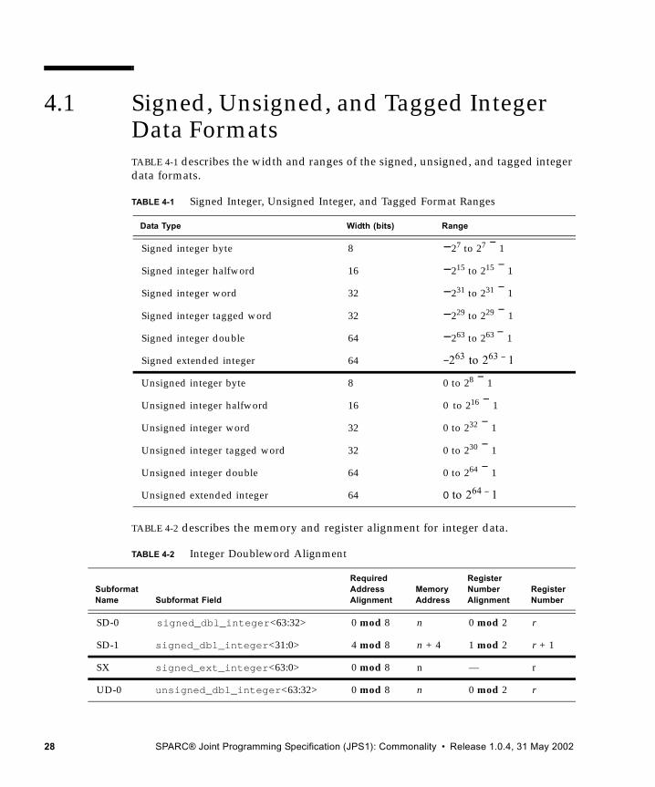
4.1 Signed, Unsigned, and Tagged Integer Data FormatsTABLE 4-1 describes the width and ranges of the signed, unsigned, and tagged integer data formats.
TABLE 4-2 describes the memory and register alignment for integer data.
TABLE 4-1 Signed Integer, Unsigned Integer, and Tagged Format Ranges
Data Type Width (bits) Range
Signed integer byte 8 −27 to 27 − 1
Signed integer halfword 16 −215 to 215 − 1
Signed integer word 32 −231 to 231 − 1
Signed integer tagged word 32 −229 to 229 − 1
Signed integer double 64 −263 to 263 − 1
Signed extended integer 64 −263 to 263 − 1
Unsigned integer byte 8 0 to 28 − 1
Unsigned integer halfword 16 0 to 216 − 1
Unsigned integer word 32 0 to 232 − 1
Unsigned integer tagged word 32 0 to 230 − 1
Unsigned integer double 64 0 to 264 − 1
Unsigned extended integer 64 0 to 264 − 1
TABLE 4-2 Integer Doubleword Alignment
Subformat Name Subformat Field
Required Address Alignment
MemoryAddress
Register Number Alignment
RegisterNumber
SD-0 signed_dbl_integer<63:32> 0 mod 8 n 0 mod 2 r
SD-1 signed_dbl_integer<31:0> 4 mod 8 n + 4 1 mod 2 r + 1
SX signed_ext_integer<63:0> 0 mod 8 n — r
UD-0 unsigned_dbl_integer<63:32> 0 mod 8 n 0 mod 2 r
28 SPARC® Joint Programming Specification (JPS1): Commonality • Release 1.0.4, 31 May 2002
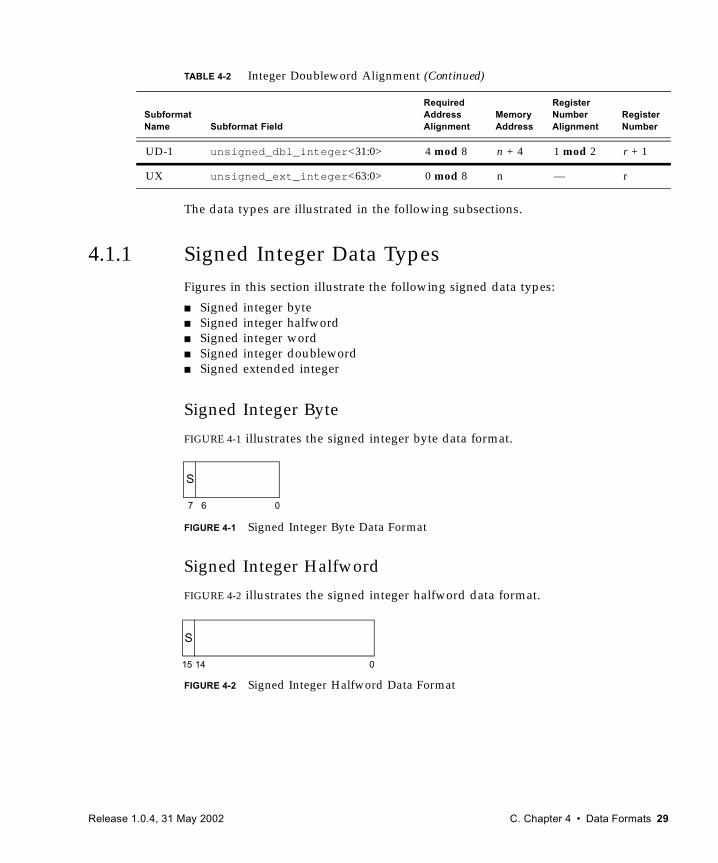
The data types are illustrated in the following subsections.
4.1.1 Signed Integer Data TypesFigures in this section illustrate the following signed data types:
■ Signed integer byte■ Signed integer halfword■ Signed integer word■ Signed integer doubleword■ Signed extended integer
Signed Integer Byte
FIGURE 4-1 illustrates the signed integer byte data format.
FIGURE 4-1 Signed Integer Byte Data Format
Signed Integer Halfword
FIGURE 4-2 illustrates the signed integer halfword data format.
FIGURE 4-2 Signed Integer Halfword Data Format
UD-1 unsigned_dbl_integer<31:0> 4 mod 8 n + 4 1 mod 2 r + 1
UX unsigned_ext_integer<63:0> 0 mod 8 n — r
TABLE 4-2 Integer Doubleword Alignment (Continued)
Subformat Name Subformat Field
Required Address Alignment
MemoryAddress
Register Number Alignment
RegisterNumber
7 6 0
S
15 14 0
S
Release 1.0.4, 31 May 2002 C. Chapter 4 • Data Formats 29
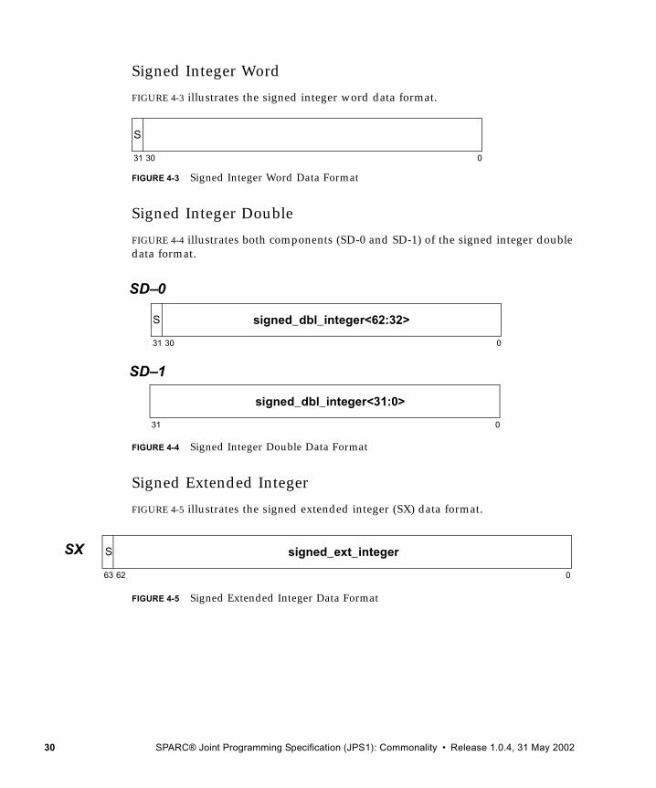
Signed Integer Word
FIGURE 4-3 illustrates the signed integer word data format.
FIGURE 4-3 Signed Integer Word Data Format
Signed Integer Double
FIGURE 4-4 illustrates both components (SD-0 and SD-1) of the signed integer double data format.
FIGURE 4-4 Signed Integer Double Data Format
Signed Extended Integer
FIGURE 4-5 illustrates the signed extended integer (SX) data format.
FIGURE 4-5 Signed Extended Integer Data Format
31 30 0
S
31 30 0
S signed_dbl_integer<62:32>
SD–0
SD–1
31 0
signed_dbl_integer<31:0>
63 62 0
S signed_ext_integerSX
30 SPARC® Joint Programming Specification (JPS1): Commonality • Release 1.0.4, 31 May 2002
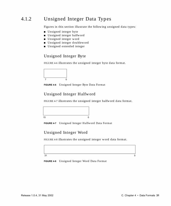
4.1.2 Unsigned Integer Data TypesFigures in this section illustrate the following unsigned data types:
■ Unsigned integer byte■ Unsigned integer halfword■ Unsigned integer word■ Unsigned integer doubleword■ Unsigned extended integer
Unsigned Integer Byte
FIGURE 4-6 illustrates the unsigned integer byte data format.
FIGURE 4-6 Unsigned Integer Byte Data Format
Unsigned Integer Halfword
FIGURE 4-7 illustrates the unsigned integer halfword data format.
FIGURE 4-7 Unsigned Integer Halfword Data Format
Unsigned Integer Word
FIGURE 4-8 illustrates the unsigned integer word data format.
FIGURE 4-8 Unsigned Integer Word Data Format
7 0
15 0
31 0
Release 1.0.4, 31 May 2002 C. Chapter 4 • Data Formats 31
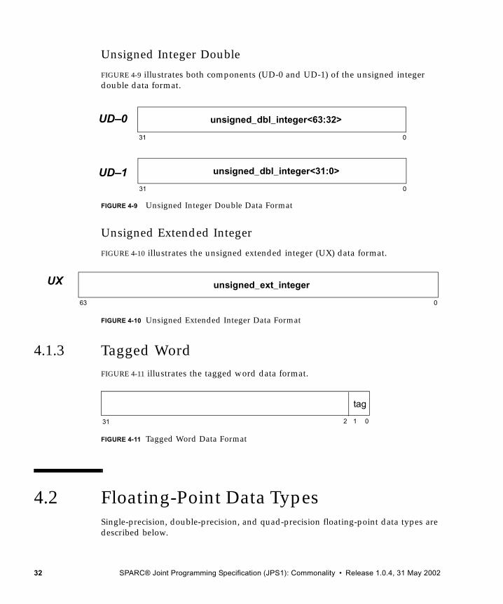
Unsigned Integer Double
FIGURE 4-9 illustrates both components (UD-0 and UD-1) of the unsigned integer double data format.
FIGURE 4-9 Unsigned Integer Double Data Format
Unsigned Extended Integer
FIGURE 4-10 illustrates the unsigned extended integer (UX) data format.
FIGURE 4-10 Unsigned Extended Integer Data Format
4.1.3 Tagged WordFIGURE 4-11 illustrates the tagged word data format.
FIGURE 4-11 Tagged Word Data Format
4.2 Floating-Point Data TypesSingle-precision, double-precision, and quad-precision floating-point data types are described below.
31 0
unsigned_dbl_integer<63:32>UD–0
UD–131 0
unsigned_dbl_integer<31:0>
63 0
unsigned_ext_integerUX
31 0
tag
2 1
32 SPARC® Joint Programming Specification (JPS1): Commonality • Release 1.0.4, 31 May 2002
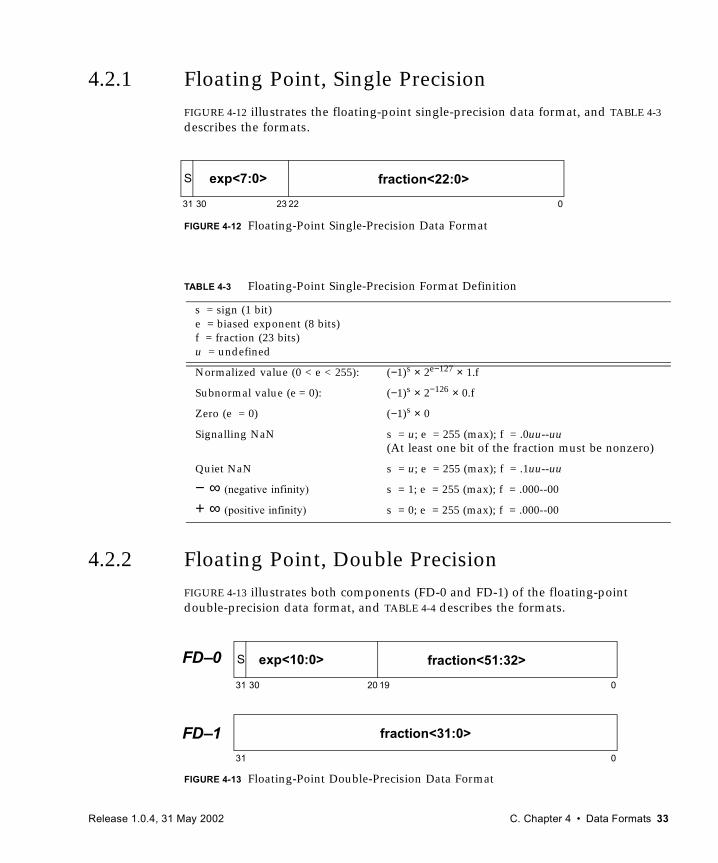
4.2.1 Floating Point, Single PrecisionFIGURE 4-12 illustrates the floating-point single-precision data format, and TABLE 4-3 describes the formats.
FIGURE 4-12 Floating-Point Single-Precision Data Format
4.2.2 Floating Point, Double PrecisionFIGURE 4-13 illustrates both components (FD-0 and FD-1) of the floating-point double-precision data format, and TABLE 4-4 describes the formats.
FIGURE 4-13 Floating-Point Double-Precision Data Format
TABLE 4-3 Floating-Point Single-Precision Format Definition
s = sign (1 bit)e = biased exponent (8 bits)f = fraction (23 bits)u = undefined
Normalized value (0 < e < 255): (−1)s × 2e−127 × 1.f
Subnormal value (e = 0): (−1)s × 2−126 × 0.f
Zero (e = 0) (−1)s × 0
Signalling NaN s = u; e = 255 (max); f = .0uu--uu(At least one bit of the fraction must be nonzero)
Quiet NaN s = u; e = 255 (max); f = .1uu--uu
− ∞ (negative infinity) s = 1; e = 255 (max); f = .000--00
+ ∞ (positive infinity) s = 0; e = 255 (max); f = .000--00
31 30 0
S exp<7:0> fraction<22:0>
2223
31 30 0
S exp<10:0> fraction<51:32>
1920
FD–0
FD–131 0
fraction<31:0>
Release 1.0.4, 31 May 2002 C. Chapter 4 • Data Formats 33
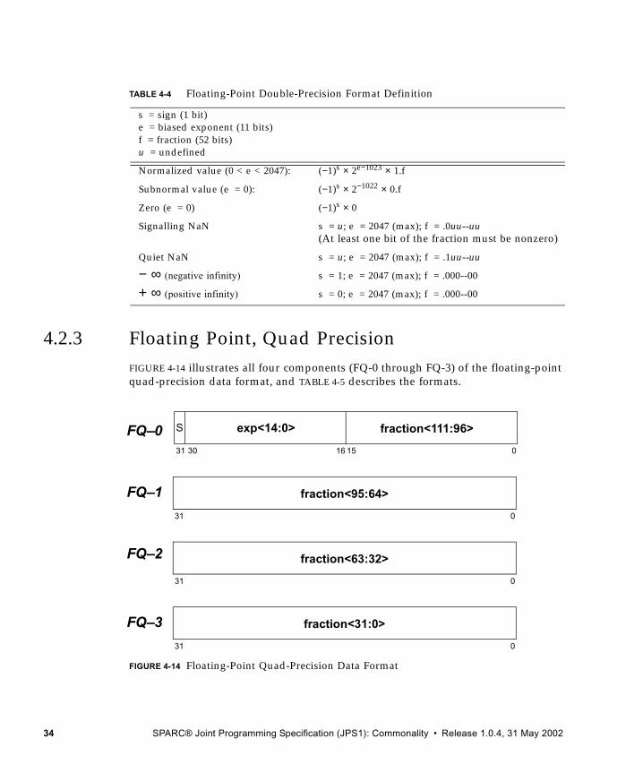
4.2.3 Floating Point, Quad PrecisionFIGURE 4-14 illustrates all four components (FQ-0 through FQ-3) of the floating-point quad-precision data format, and TABLE 4-5 describes the formats.
FIGURE 4-14 Floating-Point Quad-Precision Data Format
TABLE 4-4 Floating-Point Double-Precision Format Definition
s = sign (1 bit)e = biased exponent (11 bits)f = fraction (52 bits)u = undefined
Normalized value (0 < e < 2047): (−1)s × 2e−1023 × 1.f
Subnormal value (e = 0): (−1)s × 2−1022 × 0.f
Zero (e = 0) (−1)s × 0
Signalling NaN s = u; e = 2047 (max); f = .0uu--uu(At least one bit of the fraction must be nonzero)
Quiet NaN s = u; e = 2047 (max); f = .1uu--uu
− ∞ (negative infinity) s = 1; e = 2047 (max); f = .000--00
+ ∞ (positive infinity) s = 0; e = 2047 (max); f = .000--00
31 30 0
S exp<14:0> fraction<111:96>
1516
FQ–0
FQ–1
FQ–2
FQ–3
31 0
fraction<95:64>
31 0
fraction<63:32>
31 0
fraction<31:0>
34 SPARC® Joint Programming Specification (JPS1): Commonality • Release 1.0.4, 31 May 2002
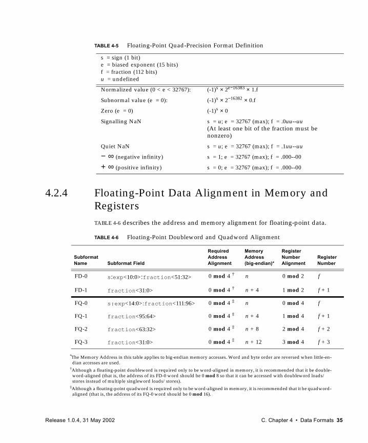
4.2.4 Floating-Point Data Alignment in Memory and RegistersTABLE 4-6 describes the address and memory alignment for floating-point data.
*The Memory Address in this table applies to big-endian memory accesses. Word and byte order are reversed when little-en-dian accesses are used.
†Although a floating-point doubleword is required only to be word-aligned in memory, it is recommended that it be double-word-aligned (that is, the address of its FD-0 word should be 0 mod 8 so that it can be accessed with doubleword loads/stores instead of multiple singleword loads/stores).
‡Although a floating-point quadword is required only to be word-aligned in memory, it is recommended that it be quadword-aligned (that is, the address of its FQ-0 word should be 0 mod 16).
TABLE 4-5 Floating-Point Quad-Precision Format Definition
s = sign (1 bit)e = biased exponent (15 bits)f = fraction (112 bits)u = undefined
Normalized value (0 < e < 32767): (-1)s × 2e−16383 × 1.f
Subnormal value (e = 0): (-1)s × 2−16382 × 0.f
Zero (e = 0) (-1)s × 0
Signalling NaN s = u; e = 32767 (max); f = .0uu--uu(At least one bit of the fraction must be nonzero)
Quiet NaN s = u; e = 32767 (max); f = .1uu--uu
− ∞ (negative infinity) s = 1; e = 32767 (max); f = .000--00
+ ∞ (positive infinity) s = 0; e = 32767 (max); f = .000--00
TABLE 4-6 Floating-Point Doubleword and Quadword Alignment
Subformat Name Subformat Field
Required Address Alignment
MemoryAddress (big-endian)*
Register Number Alignment
RegisterNumber
FD-0 s:exp<10:0>:fraction<51:32> 0 mod 4 † n 0 mod 2 f
FD-1 fraction<31:0> 0 mod 4 † n + 4 1 mod 2 f + 1
FQ-0 s:exp<14:0>:fraction<111:96> 0 mod 4 ‡ n 0 mod 4 f
FQ-1 fraction<95:64> 0 mod 4 ‡ n + 4 1 mod 4 f + 1
FQ-2 fraction<63:32> 0 mod 4 ‡ n + 8 2 mod 4 f + 2
FQ-3 fraction<31:0> 0 mod 4 ‡ n + 12 3 mod 4 f + 3
Release 1.0.4, 31 May 2002 C. Chapter 4 • Data Formats 35
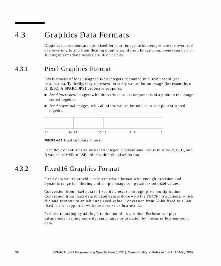
4.3 Graphics Data FormatsGraphics instructions are optimized for short integer arithmetic, where the overhead of converting to and from floating point is significant. Image components can be 8 or 16 bits; intermediate results are 16 or 32 bits.
4.3.1 Pixel Graphics FormatPixels consist of four unsigned 8-bit integers contained in a 32-bit word (see FIGURE 4-15). Typically, they represent intensity values for an image (for example, α, G, B, R). A SPARC JPS1 processor supports:
■ Band interleaved images, with the various color components of a point in the image stored together
■ Band sequential images, with all of the values for one color component stored together
FIGURE 4-15 Pixel Graphics Format
Each 8-bit quantity is an unsigned integer. Conventional use is to store α, R, G, and B values in MSB to LSB order within the pixel format.
4.3.2 Fixed16 Graphics FormatFixed data values provide an intermediate format with enough precision and dynamic range for filtering and simple image computations on pixel values.
Conversion from pixel data to fixed data occurs through pixel multiplication. Conversion from fixed data to pixel data is done with the FPACK instructions, which clip and truncate to an 8-bit unsigned value. Conversion from 32-bit fixed to 16-bit fixed is also supported with the FPACKFIX instruction.
Perform rounding by adding 1 to the round bit position. Perform complex calculations needing more dynamic range or precision by means of floating-point data.
31 24 023 16 15 8 716
36 SPARC® Joint Programming Specification (JPS1): Commonality • Release 1.0.4, 31 May 2002
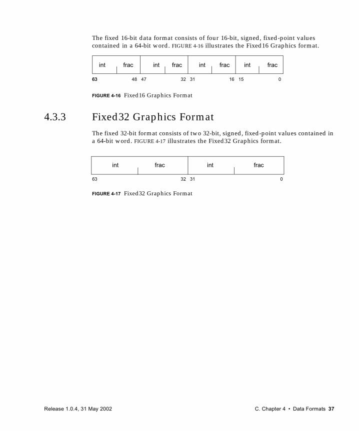
The fixed 16-bit data format consists of four 16-bit, signed, fixed-point values contained in a 64-bit word. FIGURE 4-16 illustrates the Fixed16 Graphics format.
FIGURE 4-16 Fixed16 Graphics Format
4.3.3 Fixed32 Graphics FormatThe fixed 32-bit format consists of two 32-bit, signed, fixed-point values contained in a 64-bit word. FIGURE 4-17 illustrates the Fixed32 Graphics format.
FIGURE 4-17 Fixed32 Graphics Format
63 48 0
int frac int frac int frac int frac
47 32 31 16 1563
63 0
int frac int
32 31
frac
Release 1.0.4, 31 May 2002 C. Chapter 4 • Data Formats 37

38 SPARC® Joint Programming Specification (JPS1): Commonality • Release 1.0.4, 31 May 2002
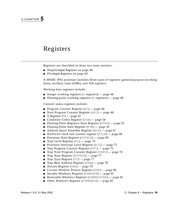
C.CHAPTER 5
Registers
Registers are described in these two main sections:
■ Nonprivileged Registers on page 40■ Privileged Registers on page 69
A SPARC JPS1 processor includes three types of registers: general-purpose (working data), ancillary state (ASRs), and ASI registers.
Working data registers include:
■ Integer working registers (r registers) — page 46■ Floating-point working registers (f registers) — page 48
Control/status registers include:
■ Program Counter Register (PC) — page 46■ Next Program Counter Register (nPC) — page 46■ Y Register (Y) — page 47■ Condition Codes Register (CCR) — page 54■ Floating-Point Registers State Register (FPRS) — page 55■ Floating-Point State Register (FSR) — page 56■ Address Space Identifier Register (ASI) — page 67■ Hardware clock-tick counter register (TICK) — page 68■ Processor State Register (PSTATE) — page 69■ Trap Level Register (TL) — page 74■ Processor Interrupt Level Register (PIL) — page 75■ Trap Program Counter Register (TPC) — page 75■ Trap Next Program Counter Register (TNPC) — page 76■ Trap State Register (TSTATE) — page 77■ Trap Type Register (TT) — page 77■ Trap Base Address Register (TBA) — page 78■ Version Register (VER) — page 79■ Current Window Pointer Register (CWP) — page 80■ Savable Windows Register (CANSAVE) — page 81■ Restorable Windows Register (CANRESTORE) — page 81■ Other Windows Register (OTHERWIN) — page 82
Release 1.0.4, 31 May 2002 C. Chapter 5 • Registers 39
■ Window State Register (WSTATE) — page 82■ Clean Windows Register (CLEANWIN) — page 83■ Performance Control Register (PCR) (ASR 16) — page 84■ Performance Instrumentation Counters (PIC) (ASR 17) — page 85■ Dispatch Control Register (DCR) (ASR 18) — page 86■ Graphics Status Register (GSR) (ASR 19) — page 87■ Set Bit(s) in Per-processor Soft Interrupt Register (SET_SOFTINT) (ASR 20) —
page 88■ Clear Bit(s) in per-processor Soft Interrupt Register (CLEAR_SOFTINT) (ASR 21)
— page 88■ Per-processor Soft Interrupt Register (SOFTINT) (ASR 22) — page 89■ Tick Compare (TICK_COMPARE) (ASR 23) — page 90■ System hardware clock-tick counter (STICK) (ASR 24) — page 90■ System Tick Compare (STICK_COMPARE) (ASR 25) — page 91■ Data Cache Unit Control Register (DCUCR) (ASI 4516) — page 92■ Virtual Address Data Watchpoint Register (ASI 5816) —page 95■ Physical Address Data Watchpoint Register (ASI 5816) — page 96■ Instruction Trap Register — page 96
The ASI registers are defined in Appendix L, Address Space Identifiers.
For convenience, some registers in this are illustrated as fewer than 64 bits wide. Any bits not shown are reserved for future extensions to the architecture. Such reserved bits are read as zeroes and, when written by software, should be written with the values of those bits previously read from that register or with zeroes.
Figures and tables in this chapter are reproduced from The SPARC Architecture Manual-Version 9.
5.1 Nonprivileged RegistersThe registers described in this subsection are visible to nonprivileged (application or “user mode”) software.
5.1.1 General-Purpose r RegistersA SPARC JPS1 processor contains 160 general-purpose 64-bit r registers. They are partitioned into eight global registers, three sets of eight alternate global registers, plus eight 16-register sets. A register window consists of the current eight in registers, eight local registers, and eight out registers. See FIGURE 5-1.
At any moment, general-purpose registers appear to nonprivileged software as shown in FIGURE 5-1.
40 SPARC® Joint Programming Specification (JPS1): Commonality • Release 1.0.4, 31 May 2002
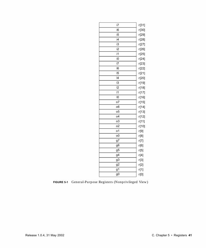
i7 r[31]
i6 r[30]
i5 r[29]
i4 r[28]
i3 r[27]
i2 r[26]
i1 r[25]
i0 r[24]
r[23]
r[22]
r[21]
r[20]
r[19]
r[18]
r[17]
r[16]
r[15]
r[14]
r[13]
r[12]
r[11]
r[10]
r[9]
r[8]
r[7]
r[6]
r[5]
r[4]
r[3]
r[2]
r[1]
r[0]
l7
l6
l5
l4
l3
l2
l1
l0
o7
o6
o5
o4
o3
o2
o1
o0
g7
g6
g5
g4
g3
g2
g1
g0
FIGURE 5-1 General-Purpose Registers (Nonprivileged View)
Release 1.0.4, 31 May 2002 C. Chapter 5 • Registers 41
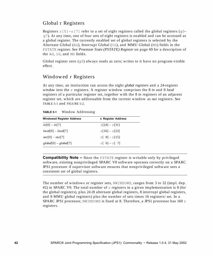
Global r Registers
Registers r[0]–r[7] refer to a set of eight registers called the global registers (g0–g7). At any time, one of four sets of eight registers is enabled and can be accessed as a global register. The currently enabled set of global registers is selected by the Alternate Global (AG), Interrupt Global (IG), and MMU Global (MG) fields in the PSTATE register. See Processor State (PSTATE) Register on page 69 for a description of the AG, IG, and MG fields.
Global register zero (g0) always reads as zero; writes to it have no program-visible effect.
Windowed r Registers
At any time, an instruction can access the eight global registers and a 24-register window into the r registers. A register window comprises the 8 in and 8 local registers of a particular register set, together with the 8 in registers of an adjacent register set, which are addressable from the current window as out registers. See TABLE 5-1 and FIGURE 5-2.
Compatibility Note – Since the PSTATE register is writable only by privileged software, existing nonprivileged SPARC V8 software operates correctly on a SPARC JPS1 processor if supervisor software ensures that nonprivileged software sees a consistent set of global registers.
The number of windows or register sets, NWINDOWS, ranges from 3 to 32 (impl. dep. #2) in SPARC V9. The total number of r registers in a given implementation is 8 (for the global registers), plus 24 (8 alternate global registers, 8 interrupt global registers, and 8 MMU global registers) plus the number of sets times 16 registers/set. In a SPARC JPS1 processor, NWINDOWS is fixed at 8. Therefore, a JPS1 processor has 160 r registers.
TABLE 5-1 Window Addressing
Windowed Register Address r Register Address
in[0] – in[7] r[24] – r[31]
local[0] – local[7] r[16] – r[23]
out[0] – out[7] r[ 8] – r[15]
global[0] – global[7] r[ 0] – r[ 7]
42 SPARC® Joint Programming Specification (JPS1): Commonality • Release 1.0.4, 31 May 2002
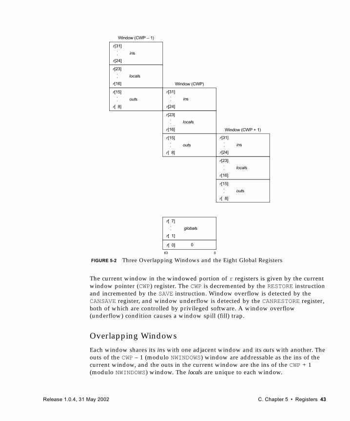
The current window in the windowed portion of r registers is given by the current window pointer (CWP) register. The CWP is decremented by the RESTORE instruction and incremented by the SAVE instruction. Window overflow is detected by the CANSAVE register, and window underflow is detected by the CANRESTORE register, both of which are controlled by privileged software. A window overflow (underflow) condition causes a window spill (fill) trap.
Overlapping Windows
Each window shares its ins with one adjacent window and its outs with another. The outs of the CWP – 1 (modulo NWINDOWS) window are addressable as the ins of the current window, and the outs in the current window are the ins of the CWP + 1 (modulo NWINDOWS) window. The locals are unique to each window.
Window (CWP – 1)
r[31]
r[24]
ins..
r[23]
r[16]
locals..
r[15]
r[ 8]
outs..
Window (CWP)
r[31]
r[24]
ins..
r[23]
r[16]
locals..
r[15]
r[ 8]
outs..
Window (CWP + 1)
r[31]
r[24]
ins..
r[23]
r[16]
locals..
r[15]
r[ 8]
outs..
r[ 7]
r[ 1]
globals..
r[ 0] 0
63 0
FIGURE 5-2 Three Overlapping Windows and the Eight Global Registers
Release 1.0.4, 31 May 2002 C. Chapter 5 • Registers 43
An outs register with address o, where 8 ≤ o ≤ 15, refers to exactly the same register as (o+16) does after the CWP is incremented by 1 (modulo NWINDOWS). Likewise, an in register with address i, where 24 ≤ i ≤ 31, refers to exactly the same register as address (i−16) does after the CWP is decremented by 1 (modulo NWINDOWS). See FIGURE 5-2 on page 43 and FIGURE 5-3 on page 45.
Since CWP arithmetic is performed modulo NWINDOWS, the highest-numbered implemented window (window 7 in SPARC JPS1) overlaps with window 0. The outs of window NWINDOWS − 1 are the ins of window 0. Implemented windows are numbered contiguously from 0 through NWINDOWS −1.
Programming Note – Since the procedure call instructions (CALL and JMPL) do not change the CWP, a procedure can be called without changing the window. See Leaf-Procedure Optimization on page 491.
Because the windows overlap, the number of windows available to software is one less than the number of implemented windows; that is, NWINDOWS – 1 or 7 in SPARC JPS1. When the register file is full, the outs of the newest window are the ins of the oldest window, which still contains valid data.
The local and out registers of a register window are guaranteed to contain either zeroes or an old value that belongs to the current context upon reentering the window through a SAVE instruction. If a program executes a RESTORE followed by a SAVE, then the resulting window’s locals and outs may not be valid after the SAVE, since a trap may have occurred between the RESTORE and the SAVE. However, if the clean_window protocol is being used, system software must guarantee that registers in the current window after a SAVE always contains only zeroes or valid data from that context. See Clean Windows (CLEANWIN) Register on page 83, Savable Windows (CANSAVE) Register on page 81, and Restorable Windows (CANRESTORE) Register on page 81.
Register Window Management Instructions on page 120 describes how the windowed integer registers are managed.
44 SPARC® Joint Programming Specification (JPS1): Commonality • Release 1.0.4, 31 May 2002
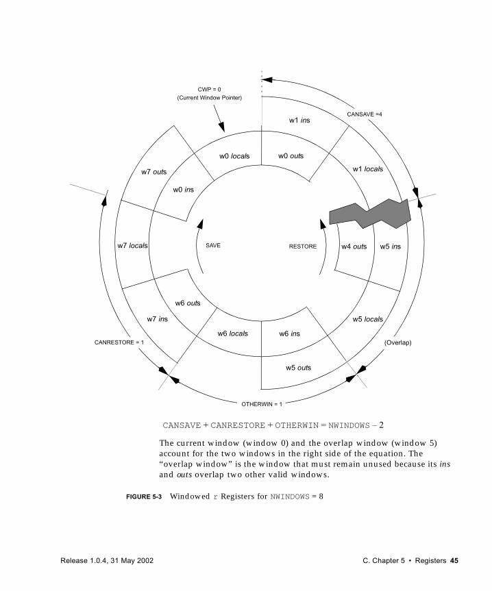
FIGURE 5-3 Windowed r Registers for NWINDOWS = 8
w4 outs
w5 outs
w6 outs
w0 outs
w7 locals
w0 ins
w1 locals
w1 ins
w6 locals w6 ins
w5 locals
OTHERWIN = 1
CANRESTORE = 1
CANSAVE + CANRESTORE + OTHERWIN = NWINDOWS – 2
The current window (window 0) and the overlap window (window 5) account for the two windows in the right side of the equation. The “overlap window” is the window that must remain unused because its ins and outs overlap two other valid windows.
SAVE RESTORE w5 ins
CANSAVE =4
(Overlap)
w0 locals
w7 outs
w7 ins
CWP = 0(Current Window Pointer)
Release 1.0.4, 31 May 2002 C. Chapter 5 • Registers 45
5.1.2 Special r RegistersThe use of two of the r registers is fixed, in whole or in part, by the architecture:
■ The value of r[0] is always zero; writes to it have no program-visible effect.
■ The CALL instruction writes its own address into register r[15] (out register 7).
Register-Pair Operands
LDD, LDDA, STD, and STDA instructions access a pair of words in adjacent r registers and require even-odd register alignment. The least significant bit of an r register number in these instructions is reserved and should be supplied as 0 by software.
When the r[0]–r[1] register pair is used as a destination in LDD or LDDA, only r[1] is modified. When the r[0]–r[1] register pair is used as a source in STD or STDA, a 0 is written to the 32-bit word at the lowest address, and the least significant 32 bits of r[1] are written to the 32-bit word at the highest address.
An attempt to execute an LDD, LDDA, STD, or STDA instruction that refers to a misaligned (odd) destination register number causes an illegal_instruction trap.
Register Usage
See General-Purpose r Registers on page 40 for information about the conventional usage of the r registers.
In FIGURE 5-3, NWINDOWS = 8. The eight global registers are not illustrated. CWP = 0, CANSAVE = 4, OTHERWIN = 1, and CANRESTORE = 1. If the procedure using window w0 executes a RESTORE, then window w7 becomes the current window. If the procedure using window w0 executes a SAVE, then window w1 becomes the current window.
5.1.3 IU Control/Status RegistersThe nonprivileged IU control/status registers include the program counters (PC and nPC), the 32-bit multiply/divide (Y) register, and several implementation-dependent Ancillary State Registers (ASRs), which are defined in Ancillary State Registers (ASRs) on page 83.
Program Counters (PC, nPC)
The PC contains the address of the instruction currently being executed. The nPC holds the address of the next instruction to be executed if a trap does not occur. The low-order two bits of PC and nPC always contain 0.
46 SPARC® Joint Programming Specification (JPS1): Commonality • Release 1.0.4, 31 May 2002
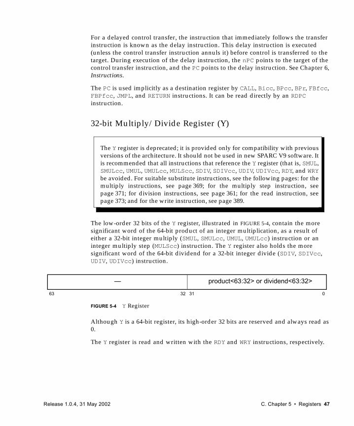
For a delayed control transfer, the instruction that immediately follows the transfer instruction is known as the delay instruction. This delay instruction is executed (unless the control transfer instruction annuls it) before control is transferred to the target. During execution of the delay instruction, the nPC points to the target of the control transfer instruction, and the PC points to the delay instruction. See Chapter 6, Instructions.
The PC is used implicitly as a destination register by CALL, Bicc, BPcc, BPr, FBfcc, FBPfcc, JMPL, and RETURN instructions. It can be read directly by an RDPC instruction.
32-bit Multiply/Divide Register (Y)
The low-order 32 bits of the Y register, illustrated in FIGURE 5-4, contain the more significant word of the 64-bit product of an integer multiplication, as a result of either a 32-bit integer multiply (SMUL, SMULcc, UMUL, UMULcc) instruction or an integer multiply step (MULScc) instruction. The Y register also holds the more significant word of the 64-bit dividend for a 32-bit integer divide (SDIV, SDIVcc, UDIV, UDIVcc) instruction.
FIGURE 5-4 Y Register
Although Y is a 64-bit register, its high-order 32 bits are reserved and always read as 0.
The Y register is read and written with the RDY and WRY instructions, respectively.
The Y register is deprecated; it is provided only for compatibility with previousversions of the architecture. It should not be used in new SPARC V9 software. Itis recommended that all instructions that reference the Y register (that is, SMUL,SMULcc, UMUL, UMULcc, MULScc, SDIV, SDIVcc, UDIV, UDIVcc, RDY, and WRYbe avoided. For suitable substitute instructions, see the following pages: for themultiply instructions, see page 369; for the multiply step instruction, seepage 371; for division instructions, see page 361; for the read instruction, seepage 373; and for the write instruction, see page 389.
63 032 31
— product<63:32> or dividend<63:32>
Release 1.0.4, 31 May 2002 C. Chapter 5 • Registers 47
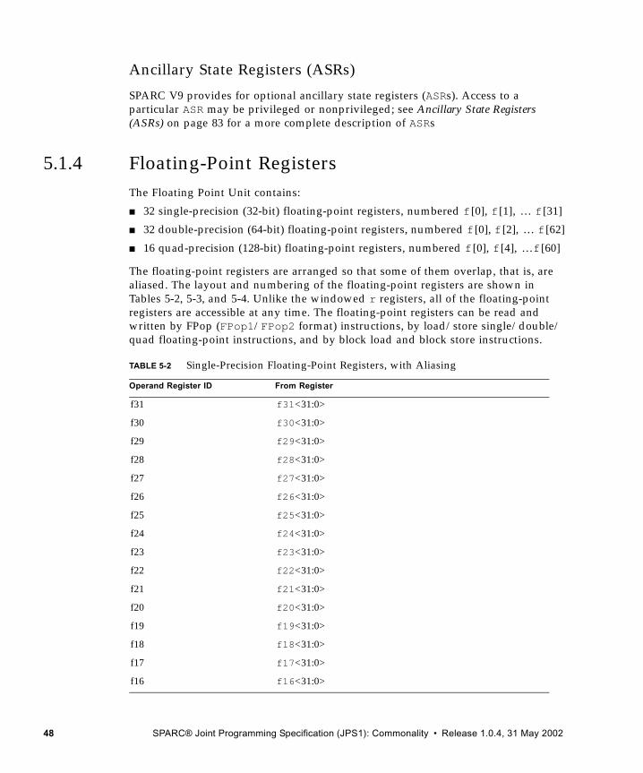
Ancillary State Registers (ASRs)
SPARC V9 provides for optional ancillary state registers (ASRs). Access to a particular ASR may be privileged or nonprivileged; see Ancillary State Registers (ASRs) on page 83 for a more complete description of ASRs
5.1.4 Floating-Point RegistersThe Floating Point Unit contains:
■ 32 single-precision (32-bit) floating-point registers, numbered f [0], f[1], … f[31]
■ 32 double-precision (64-bit) floating-point registers, numbered f[0], f [2], … f[62]
■ 16 quad-precision (128-bit) floating-point registers, numbered f [0], f[4], …f [60]
The floating-point registers are arranged so that some of them overlap, that is, are aliased. The layout and numbering of the floating-point registers are shown in Tables 5-2, 5-3, and 5-4. Unlike the windowed r registers, all of the floating-point registers are accessible at any time. The floating-point registers can be read and written by FPop (FPop1/FPop2 format) instructions, by load/store single/double/quad floating-point instructions, and by block load and block store instructions.
TABLE 5-2 Single-Precision Floating-Point Registers, with Aliasing
Operand Register ID From Register
f31 f31<31:0>
f30 f30<31:0>
f29 f29<31:0>
f28 f28<31:0>
f27 f27<31:0>
f26 f26<31:0>
f25 f25<31:0>
f24 f24<31:0>
f23 f23<31:0>
f22 f22<31:0>
f21 f21<31:0>
f20 f20<31:0>
f19 f19<31:0>
f18 f18<31:0>
f17 f17<31:0>
f16 f16<31:0>
48 SPARC® Joint Programming Specification (JPS1): Commonality • Release 1.0.4, 31 May 2002
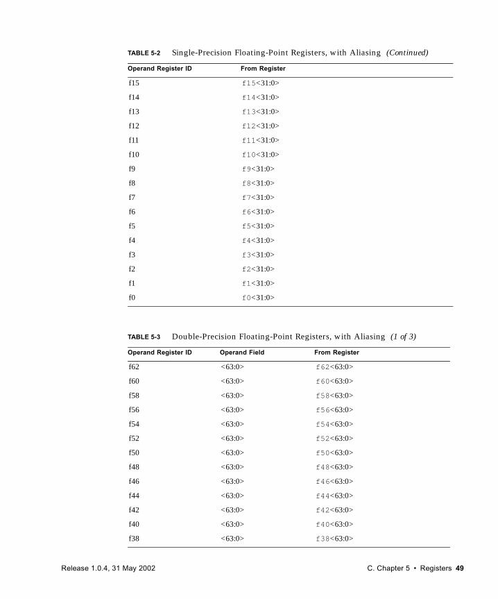
f15 f15<31:0>
f14 f14<31:0>
f13 f13<31:0>
f12 f12<31:0>
f11 f11<31:0>
f10 f10<31:0>
f9 f9<31:0>
f8 f8<31:0>
f7 f7<31:0>
f6 f6<31:0>
f5 f5<31:0>
f4 f4<31:0>
f3 f3<31:0>
f2 f2<31:0>
f1 f1<31:0>
f0 f0<31:0>
TABLE 5-3 Double-Precision Floating-Point Registers, with Aliasing (1 of 3)
Operand Register ID Operand Field From Register
f62 <63:0> f62<63:0>
f60 <63:0> f60<63:0>
f58 <63:0> f58<63:0>
f56 <63:0> f56<63:0>
f54 <63:0> f54<63:0>
f52 <63:0> f52<63:0>
f50 <63:0> f50<63:0>
f48 <63:0> f48<63:0>
f46 <63:0> f46<63:0>
f44 <63:0> f44<63:0>
f42 <63:0> f42<63:0>
f40 <63:0> f40<63:0>
f38 <63:0> f38<63:0>
TABLE 5-2 Single-Precision Floating-Point Registers, with Aliasing (Continued)
Operand Register ID From Register
Release 1.0.4, 31 May 2002 C. Chapter 5 • Registers 49
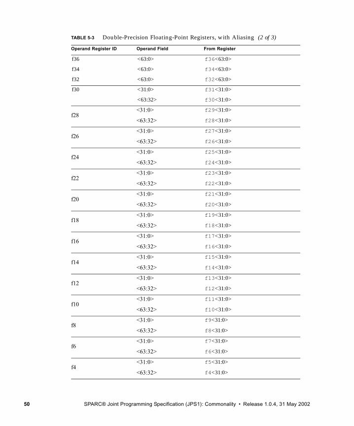
f36 <63:0> f36<63:0>
f34 <63:0> f34<63:0>
f32 <63:0> f32<63:0>
f30 <31:0> f31<31:0>
<63:32> f30<31:0>
f28<31:0> f29<31:0>
<63:32> f28<31:0>
f26<31:0> f27<31:0>
<63:32> f26<31:0>
f24<31:0> f25<31:0>
<63:32> f24<31:0>
f22<31:0> f23<31:0>
<63:32> f22<31:0>
f20<31:0> f21<31:0>
<63:32> f20<31:0>
f18<31:0> f19<31:0>
<63:32> f18<31:0>
f16<31:0> f17<31:0>
<63:32> f16<31:0>
f14<31:0> f15<31:0>
<63:32> f14<31:0>
f12<31:0> f13<31:0>
<63:32> f12<31:0>
f10<31:0> f11<31:0>
<63:32> f10<31:0>
f8<31:0> f9<31:0>
<63:32> f8<31:0>
f6<31:0> f7<31:0>
<63:32> f6<31:0>
f4<31:0> f5<31:0>
<63:32> f4<31:0>
TABLE 5-3 Double-Precision Floating-Point Registers, with Aliasing (2 of 3)
Operand Register ID Operand Field From Register
50 SPARC® Joint Programming Specification (JPS1): Commonality • Release 1.0.4, 31 May 2002
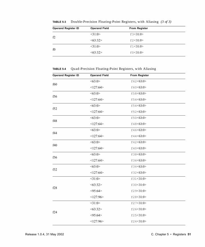
f2<31:0> f3<31:0>
<63:32> f2<31:0>
f0<31:0> f1<31:0>
<63:32> f0<31:0>
TABLE 5-4 Quad-Precision Floating-Point Registers, with Aliasing
Operand Register ID Operand Field From Register
f60<63:0> f62<63:0>
<127:64> f60<63:0>
f56<63:0> f58<63:0>
<127:64> f56<63:0>
f52<63:0> f54<63:0>
<127:64> f52<63:0>
f48<63:0> f50<63:0>
<127:64> f48<63:0>
f44<63:0> f46<63:0>
<127:64> f44<63:0>
f40<63:0> f42<63:0>
<127:64> f40<63:0>
f36<63:0> f38<63:0>
<127:64> f36<63:0>
f32<63:0> f34<63:0>
<127:64> f32<63:0>
f28
<31:0> f31<31:0>
<63:32> f30<31:0>
<95:64> f29<31:0>
<127:96> f28<31:0>
f24
<31:0> f27<31:0>
<63:32> f26<31:0>
<95:64> f25<31:0>
<127:96> f24<31:0>
TABLE 5-3 Double-Precision Floating-Point Registers, with Aliasing (3 of 3)
Operand Register ID Operand Field From Register
Release 1.0.4, 31 May 2002 C. Chapter 5 • Registers 51
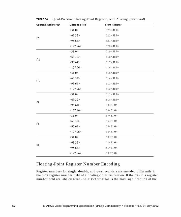
Floating-Point Register Number Encoding
Register numbers for single, double, and quad registers are encoded differently in the 5-bit register number field of a floating-point instruction. If the bits in a register number field are labeled b<4>–b<0> (where b<4> is the most significant bit of the
f20
<31:0> f23<31:0>
<63:32> f22<31:0>
<95:64> f21<31:0>
<127:96> f20<31:0>
f16
<31:0> f19<31:0>
<63:32> f18<31:0>
<95:64> f17<31:0>
<127:96> f16<31:0>
f12
<31:0> f15<31:0>
<63:32> f14<31:0>
<95:64> f13<31:0>
<127:96> f12<31:0>
f8
<31:0> f11<31:0>
<63:32> f10<31:0>
<95:64> f9<31:0>
<127:96> f8<31:0>
f4
<31:0> f7<31:0>
<63:32> f6<31:0>
<95:64> f5<31:0>
<127:96> f4<31:0>
f0
<31:0> f3<31:0>
<63:32> f2<31:0>
<95:64> f1<31:0>
<127:96> f0<31:0>
TABLE 5-4 Quad-Precision Floating-Point Registers, with Aliasing (Continued)
Operand Register ID Operand Field From Register
52 SPARC® Joint Programming Specification (JPS1): Commonality • Release 1.0.4, 31 May 2002
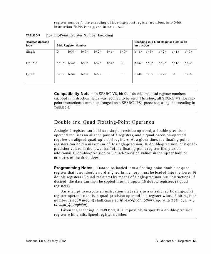
register number), the encoding of floating-point register numbers into 5-bit instruction fields is as given in TABLE 5-5.
Compatibility Note – In SPARC V8, bit 0 of double and quad register numbers encoded in instruction fields was required to be zero. Therefore, all SPARC V8 floating-point instructions can run unchanged on a SPARC JPS1 processor, using the encoding in TABLE 5-5.
Double and Quad Floating-Point Operands
A single f register can hold one single-precision operand; a double-precision operand requires an aligned pair of f registers, and a quad-precision operand requires an aligned quadruple of f registers. At a given time, the floating-point registers can hold a maximum of 32 single-precision, 16 double-precision, or 8 quad-precision values in the lower half of the floating-point register file, plus an additional 16 double-precision or 8 quad-precision values in the upper half, or mixtures of the three sizes.
Programming Notes – Data to be loaded into a floating-point double or quad register that is not doubleword aligned in memory must be loaded into the lower 16 double registers (8 quad registers) by means of single-precision LDF instructions. If desired, the data can then be copied into the upper 16 double registers (8 quad registers).
An attempt to execute an instruction that refers to a misaligned floating-point register operand (that is, a quad-precision operand in a register whose 6-bit register number is not 0 mod 4) shall cause an fp_exception_other trap, with FSR.ftt = 6 (invalid_fp_register).
Given the encoding in TABLE 5-5, it is impossible to specify a double-precision register with a misaligned register number.
TABLE 5-5 Floating-Point Register Number Encoding
Register Operand Type 6-bit Register Number
Encoding in a 5-bit Register Field in an Instruction
Single 0 b<4> b<3> b<2> b<1> b<0> b<4> b<3> b<2> b<1> b<0>
Double b<5> b<4> b<3> b<2> b<1> 0 b<4> b<3> b<2> b<1> b<5>
Quad b<5> b<4> b<3> b<2> 0 0 b<4> b<3> b<2> 0 b<5>
Release 1.0.4, 31 May 2002 C. Chapter 5 • Registers 53
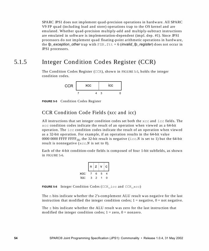
SPARC JPS1 does not implement quad-precision operations in hardware. All SPARC V9 FP quad (including load and store) operations trap to the OS kernel and are emulated. Whether quad-precision multiply-add and multiply-subtract instructions are emulated in software is implementation-dependent (impl. dep. #1). Since JPS1 processors do not implement quad floating-point arithmetic operations in hardware, the fp_exception_other trap with FSR.ftt = 6 (invalid_fp_register) does not occur in JPS1 processors.
5.1.5 Integer Condition Codes Register (CCR)The Condition Codes Register (CCR), shown in FIGURE 5-5, holds the integer condition codes.
FIGURE 5-5 Condition Codes Register
CCR Condition Code Fields (xcc and icc)
All instructions that set integer condition codes set both the xcc and icc fields. The xcc condition codes indicate the result of an operation when viewed as a 64-bit operation. The icc condition codes indicate the result of an operation when viewed as a 32-bit operation. For example, if an operation results in the 64-bit value 0000 0000 FFFF FFFF16, the 32-bit result is negative (icc.N is set to 1) but the 64-bit result is nonnegative (xcc.N is set to 0).
Each of the 4-bit condition-code fields is composed of four 1-bit subfields, as shown in FIGURE 5-6.
FIGURE 5-6 Integer Condition Codes (CCR_icc and CCR_xcc)
The n bits indicate whether the 2’s-complement ALU result was negative for the last instruction that modified the integer condition codes; 1 = negative, 0 = not negative.
The z bits indicate whether the ALU result was zero for the last instruction that modified the integer condition codes; 1 = zero, 0 = nonzero.
7 4 03
xcc iccCCR
7 5 4
0
6
13 2
xcc:icc:
cvn z
54 SPARC® Joint Programming Specification (JPS1): Commonality • Release 1.0.4, 31 May 2002
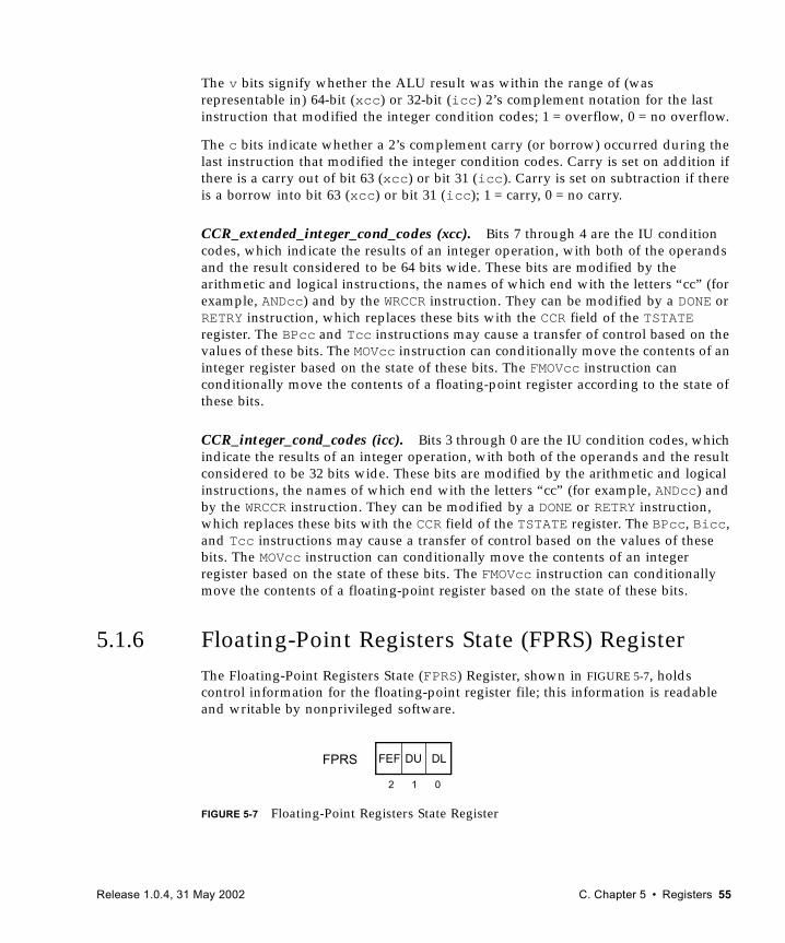
The v bits signify whether the ALU result was within the range of (was representable in) 64-bit (xcc) or 32-bit (icc) 2’s complement notation for the last instruction that modified the integer condition codes; 1 = overflow, 0 = no overflow.
The c bits indicate whether a 2’s complement carry (or borrow) occurred during the last instruction that modified the integer condition codes. Carry is set on addition if there is a carry out of bit 63 (xcc) or bit 31 (icc). Carry is set on subtraction if there is a borrow into bit 63 (xcc) or bit 31 (icc); 1 = carry, 0 = no carry.
CCR_extended_integer_cond_codes (xcc). Bits 7 through 4 are the IU condition codes, which indicate the results of an integer operation, with both of the operands and the result considered to be 64 bits wide. These bits are modified by the arithmetic and logical instructions, the names of which end with the letters “cc” (for example, ANDcc) and by the WRCCR instruction. They can be modified by a DONE or RETRY instruction, which replaces these bits with the CCR field of the TSTATE register. The BPcc and Tcc instructions may cause a transfer of control based on the values of these bits. The MOVcc instruction can conditionally move the contents of an integer register based on the state of these bits. The FMOVcc instruction can conditionally move the contents of a floating-point register according to the state of these bits.
CCR_integer_cond_codes (icc). Bits 3 through 0 are the IU condition codes, which indicate the results of an integer operation, with both of the operands and the result considered to be 32 bits wide. These bits are modified by the arithmetic and logical instructions, the names of which end with the letters “cc” (for example, ANDcc) and by the WRCCR instruction. They can be modified by a DONE or RETRY instruction, which replaces these bits with the CCR field of the TSTATE register. The BPcc, Bicc, and Tcc instructions may cause a transfer of control based on the values of these bits. The MOVcc instruction can conditionally move the contents of an integer register based on the state of these bits. The FMOVcc instruction can conditionally move the contents of a floating-point register based on the state of these bits.
5.1.6 Floating-Point Registers State (FPRS) RegisterThe Floating-Point Registers State (FPRS) Register, shown in FIGURE 5-7, holds control information for the floating-point register file; this information is readable and writable by nonprivileged software.
FIGURE 5-7 Floating-Point Registers State Register
012
DLFEF DUFPRS
Release 1.0.4, 31 May 2002 C. Chapter 5 • Registers 55
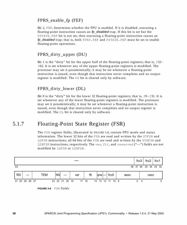
FPRS_enable_fp (FEF)
Bit 2, FEF, determines whether the FPU is enabled. If it is disabled, executing a floating-point instruction causes an fp_disabled trap. If this bit is set but the PSTATE.PEF bit is not set, then executing a floating-point instruction causes an fp_disabled trap; that is, both FPRS.FEF and PSTATE.PEF must be set to enable floating-point operations.
FPRS_dirty_upper (DU)
Bit 1 is the “dirty” bit for the upper half of the floating-point registers; that is, f32–f62. It is set whenever any of the upper floating-point registers is modified. The processor may set it pessimistically; it may be set whenever a floating-point instruction is issued, even though that instruction never completes and no output register is modified. The DU bit is cleared only by software.
FPRS_dirty_lower (DL)
Bit 0 is the “dirty” bit for the lower 32 floating-point registers; that is, f0–f31. It is set whenever any of the lower floating-point registers is modified. The processor may set it pessimistically; it may be set whenever a floating-point instruction is issued, even though that instruction never completes and no output register is modified. The DL bit is cleared only by software.
5.1.7 Floating-Point State Register (FSR)The FSR register fields, illustrated in FIGURE 5-8, contain FPU mode and status information. The lower 32 bits of the FSR are read and written by the STFSR and LDFSR instructions; all 64 bits of the FSR are read and written by the STXFSR and LDXFSR instructions, respectively. The ver, ftt, and reserved (“—”) fields are not modified by LDFSR or LDXFSR.
FIGURE 5-8 FSR Fields
63 3235 34 3338 37
31 141923 13 12 11 5 4 091017 162730 29 28 22 21 20
36
fcc3 fcc2 fcc1—
RD — TEM NS — ver ftt qne — fcc0 aexc cexc
56 SPARC® Joint Programming Specification (JPS1): Commonality • Release 1.0.4, 31 May 2002
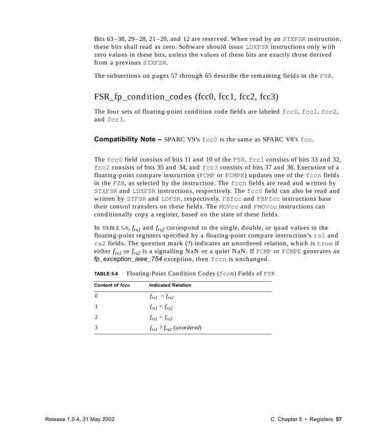
Bits 63–38, 29–28, 21–20, and 12 are reserved. When read by an STXFSR instruction, these bits shall read as zero. Software should issue LDXFSR instructions only with zero values in these bits, unless the values of these bits are exactly those derived from a previous STXFSR.
The subsections on pages 57 through 65 describe the remaining fields in the FSR.
FSR_fp_condition_codes (fcc0, fcc1, fcc2, fcc3)
The four sets of floating-point condition code fields are labeled fcc0, fcc1, fcc2, and fcc3.
Compatibility Note – SPARC V9’s fcc0 is the same as SPARC V8’s fcc.
The fcc0 field consists of bits 11 and 10 of the FSR, fcc1 consists of bits 33 and 32, fcc2 consists of bits 35 and 34, and fcc3 consists of bits 37 and 36. Execution of a floating-point compare instruction (FCMP or FCMPE) updates one of the fccn fields in the FSR, as selected by the instruction. The fccn fields are read and written by STXFSR and LDXFSR instructions, respectively. The fcc0 field can also be read and written by STFSR and LDFSR, respectively. FBfcc and FBPfcc instructions base their control transfers on these fields. The MOVcc and FMOVcc instructions can conditionally copy a register, based on the state of these fields.
In TABLE 5-6, frs1 and frs2 correspond to the single, double, or quad values in the floating-point registers specified by a floating-point compare instruction’s rs1 and rs2 fields. The question mark (?) indicates an unordered relation, which is true if either frs1 or frs2 is a signalling NaN or a quiet NaN. If FCMP or FCMPE generates an fp_exception_ieee_754 exception, then fccn is unchanged.
TABLE 5-6 Floating-Point Condition Codes (fccn) Fields of FSR
Content of fccn Indicated Relation
0 frs1 = frs2
1 frs1 < frs2
2 frs1 > frs2
3 frs1 ? frs2 (unordered)
Release 1.0.4, 31 May 2002 C. Chapter 5 • Registers 57
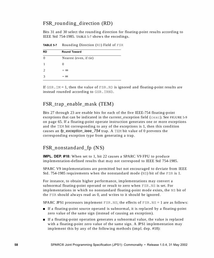
FSR_rounding_direction (RD)
Bits 31 and 30 select the rounding direction for floating-point results according to IEEE Std 754-1985. TABLE 5-7 shows the encodings.
If GSR.IM = 1, then the value of FSR.RD is ignored and floating-point results are instead rounded according to GSR.IRND.
FSR_trap_enable_mask (TEM)
Bits 27 through 23 are enable bits for each of the five IEEE-754 floating-point exceptions that can be indicated in the current_exception field (cexc). See FIGURE 5-9 on page 65. If a floating-point operate instruction generates one or more exceptions and the TEM bit corresponding to any of the exceptions is 1, then this condition causes an fp_exception_ieee_754 trap. A TEM bit value of 0 prevents the corresponding exception type from generating a trap.
FSR_nonstandard_fp (NS)
IMPL. DEP. #18: When set to 1, bit 22 causes a SPARC V9 FPU to produce implementation-defined results that may not correspond to IEEE Std 754-1985.
SPARC V9 implementations are permitted but not encouraged to deviate from IEEE Std. 754-1985 requirements when the nonstandard mode (NS) bit of the FSR is 1.
For instance, to obtain higher performance, implementations may convert a subnormal floating-point operand or result to zero when FSR.NS is set. For implementations in which no nonstandard floating-point mode exists, the NS bit of the FSR should always read as 0, and writes to it should be ignored.
SPARC JPS1 processors implement FSR.NS; the effects of FSR.NS = 1 are as follows:
■ If a floating-point source operand is subnormal, it is replaced by a floating-point zero value of the same sign (instead of causing an exception).
■ If a floating-point operation generates a subnormal value, the value is replaced with a floating-point zero value of the same sign. A JPS1 implementation may implement this by any of the following methods (impl. dep. #18):
TABLE 5-7 Rounding Direction (RD) Field of FSR
RD Round Toward
0 Nearest (even, if tie)
1 0
2 + ∞
3 − ∞
58 SPARC® Joint Programming Specification (JPS1): Commonality • Release 1.0.4, 31 May 2002
■ Always perform the replacement in hardware, never causing an exception.
■ Always perform the replacement in hardware, but also cause an fp_exception__ieee754 “inexact,” ”underflow,” or “division-by-zero” exception (which may be masked with FSR.TEM).
■ Sometimes perform the replacement in hardware, and sometimes cause an fp_exception_other exception with FSR.ftt = 2 (unfinished_FPop) so that trap handler software can perform the replacement.
If GSR.IM = 1, then the value of FSR.NS is ignored and the processor operates as if FSR.NS = 0.
FSR_version (ver)
IMPL. DEP. #19: Bits 19 through 17 identify one or more particular implementations of the FPU architecture.
For each SPARC V9 IU implementation (as identified by its VER.impl field), there may be one or more FPU implementations, or none. This field identifies the particular FPU implementation present. The value in FSR.ver for each implementation is strictly implementation dependent. Consult the appropriate document for each implementation for its setting of FSR.ver.
Version number 7 is reserved to indicate that no hardware floating-point controller is present.
The ver field is read-only; it cannot be modified by the LDFSR and LDXFSR instructions.
FSR_floating-point_trap_type (ftt)
Several conditions can cause a floating-point exception trap. When a floating-point exception trap occurs, ftt (bits 16 through 14 of the FSR) identifies the cause of the exception, the “floating-point trap type.” After a floating-point exception occurs, the ftt field encodes the type of the floating-point exception until an STFSR or an FPop is executed.
The ftt field can be read by the STFSR and STXFSR instructions. The LDFSR and LDXFSR instructions do not affect ftt.
Privileged software that handles floating-point traps must execute an STFSR (or STXFSR) to determine the floating-point trap type. STFSR and STXFSR shall zero ftt after the store completes without error. If the store generates an error and does not complete, ftt remains unchanged.
Release 1.0.4, 31 May 2002 C. Chapter 5 • Registers 59
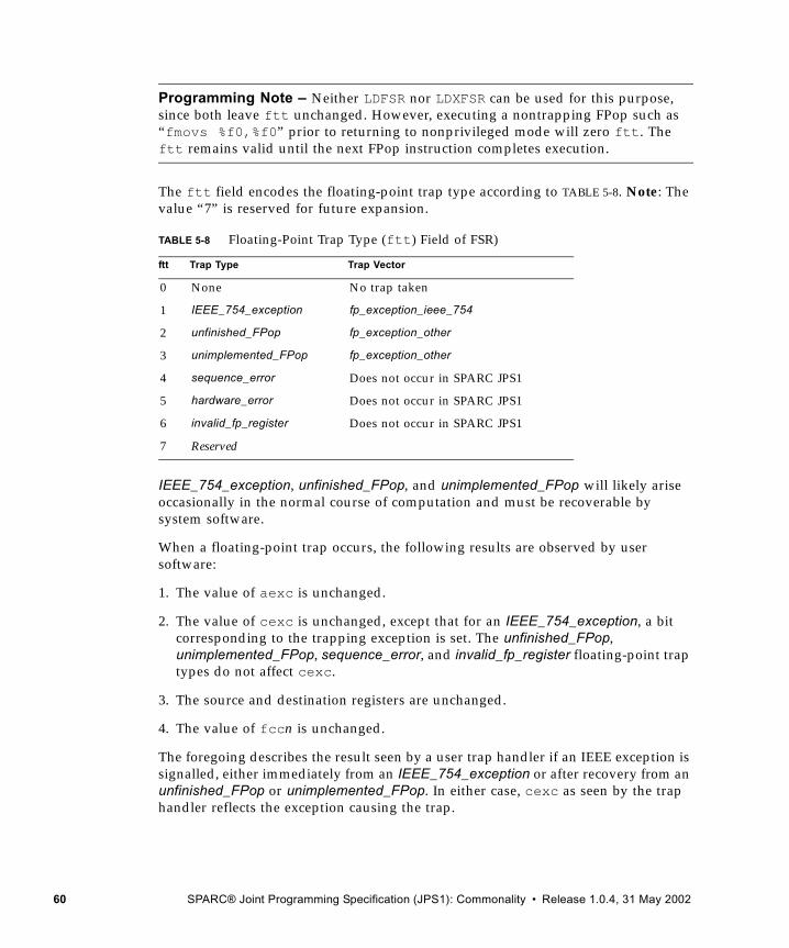
Programming Note – Neither LDFSR nor LDXFSR can be used for this purpose, since both leave ftt unchanged. However, executing a nontrapping FPop such as “fmovs %f0,%f0” prior to returning to nonprivileged mode will zero ftt. The ftt remains valid until the next FPop instruction completes execution.
The ftt field encodes the floating-point trap type according to TABLE 5-8. Note: The value “7” is reserved for future expansion.
IEEE_754_exception, unfinished_FPop, and unimplemented_FPop will likely arise occasionally in the normal course of computation and must be recoverable by system software.
When a floating-point trap occurs, the following results are observed by user software:
1. The value of aexc is unchanged.
2. The value of cexc is unchanged, except that for an IEEE_754_exception, a bit corresponding to the trapping exception is set. The unfinished_FPop, unimplemented_FPop, sequence_error, and invalid_fp_register floating-point trap types do not affect cexc.
3. The source and destination registers are unchanged.
4. The value of fccn is unchanged.
The foregoing describes the result seen by a user trap handler if an IEEE exception is signalled, either immediately from an IEEE_754_exception or after recovery from an unfinished_FPop or unimplemented_FPop. In either case, cexc as seen by the trap handler reflects the exception causing the trap.
TABLE 5-8 Floating-Point Trap Type (ftt) Field of FSR)
ftt Trap Type Trap Vector
0 None No trap taken
1 IEEE_754_exception fp_exception_ieee_754
2 unfinished_FPop fp_exception_other
3 unimplemented_FPop fp_exception_other
4 sequence_error Does not occur in SPARC JPS1
5 hardware_error Does not occur in SPARC JPS1
6 invalid_fp_register Does not occur in SPARC JPS1
7 Reserved
60 SPARC® Joint Programming Specification (JPS1): Commonality • Release 1.0.4, 31 May 2002
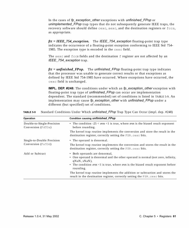
In the cases of fp_exception_other exceptions with unfinished_FPop or unimplemented_FPop trap types that do not subsequently generate IEEE traps, the recovery software should define cexc, aexc, and the destination registers or fccs, as appropriate.
ftt = IEEE_754_exception. The IEEE_754_exception floating-point trap type indicates the occurrence of a floating-point exception conforming to IEEE Std 754-1985. The exception type is encoded in the cexc field.
The aexc and fccs fields and the destination f register are not affected by an IEEE_754_exception trap.
ftt = unfinished_FPop. The unfinished_FPop floating-point trap type indicates that the processor was unable to generate correct results or that exceptions as defined by IEEE Std 754-1985 have occurred. Where exceptions have occurred, the cexc field is unchanged.
IMPL. DEP. #248: The conditions under which an fp_exception_other exception with floating-point trap type of unfinished_FPop can occur are implementation dependent. The standard (recommended) set of conditions is listed in TABLE 5-9. An implementation may cause fp_exception_other with unfinished_FPop under a different (but specified) set of conditions.
TABLE 5-9 Standard Conditions Under Which unfinished_FPop Trap Type Can Occur (impl. dep. #248)
Operation Condition causing unfinished_FPop
Double-to-Single-Precision Conversion (FdTOs)
• The condition -25 < eres <1 is true, where eres is the biased result exponent before rounding.
The kernel trap routine implements the conversion and store the result in the destination register, correctly setting the FSR.cexc bits.
Single-to-Double Precision Conversion (FsTOd)
• The operand is denormal.The kernel trap routine implements the conversion and stores the result in the destination register, correctly setting the FSR.cexc bits.
Add or Subtract • Both operands are denormal,• One operand is denormal and the other operand is normal (not zero, infinity,
qNaN, sNaN),• The condition eres <1 is true, where eres is the biased result exponent before
rounding.The kernel trap routine implements the addition or subtraction and stores the result in the destination register, correctly setting the FSR.cexc bits.
Release 1.0.4, 31 May 2002 C. Chapter 5 • Registers 61
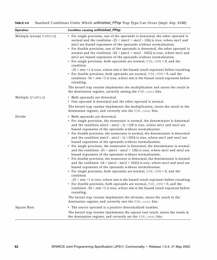
Multiply (except FsMULd) • For single precision, one of the operands is denormal, the other operand is normal and the condition -25 < (esrc1 + esrc2 - 126) is true, where esrc1 and esrc2 are biased exponents of the operands without normalization.
• For double precision, one of the operands is denormal, the other operand is normal and the condition -54 < (esrc1 + esrc2 - 1022) is true, where esrc1 and esrc2 are biased exponents of the operands without normalization.
• For single precision, both operands are normal, FSR.UFM = 0, and the condition -25 < eres <1 is true, where eres is the biased result exponent before rounding.
• For double precision, both operands are normal, FSR.UFM = 0, and the condition -54 < eres <1 is true, where eres is the biased result exponent before rounding.
The kernel trap routine implements the multiplication and stores the result in the destination register, correctly setting the FSR.cexc bits.
Multiply (FsMULd) • Both operands are denormal.• One operand is denormal and the other operand is normal.The kernel trap routine implements the multiplication, stores the result in the destination register, and correctly sets the FSR.cexc bits.
Divide • Both operands are denormal.• For single precision, the numerator is normal, the denominator is denormal
and the condition (esrc1 - esrc2 - 1) <128 is true, where esrc1 and esrc2 are biased exponents of the operands without normalization.
• For double precision, the numerator is normal, the denominator is denormal and the condition (esrc1 - esrc2 - 1) <1024 is true, where esrc1 and esrc2 are biased exponents of the operands without normalization.
• For single precision, the numerator is denormal, the denominator is normal and the condition -25 < (esrc1 - esrc2 + 126) is true, where esrc1 and esrc2 are biased exponents of the operands without normalization.
• For double precision, the numerator is denormal, the denominator is normal and the condition -54 < (esrc1 - esrc2 + 1022) is true, where esrc1 and esrc2 are biased exponents of the operands without normalization.
• For single precision, both operands are normal, FSR.UFM = 0, and the condition -25 < eres <1 is true, where eres is the biased result exponent before rounding.
• For double precision, both operands are normal, FSR.UFM = 0, and the condition -54 < eres <1 is true, where eres is the biased result exponent before rounding.
The kernel trap routine implements the division, stores the result in the destination register, and correctly sets the FSR.cexc bits.
Square Root • The source operand is a positive denormalized number.The kernel trap routine implements the square root result, stores the result in the destination register, and correctly set the FSR.cexc bits.
TABLE 5-9 Standard Conditions Under Which unfinished_FPop Trap Type Can Occur (impl. dep. #248)
Operation Condition causing unfinished_FPop
62 SPARC® Joint Programming Specification (JPS1): Commonality • Release 1.0.4, 31 May 2002
ftt = unimplemented_FPop. The unimplemented_FPop floating-point trap type indicates that the processor decoded an FPop that it does not implement. In this case, the cexc field is unchanged.
All quad FPop variations in a SPARC JPS1 processor set ftt = unimplemented_FPop.
ftt = sequence_error. The sequence_error floating-point trap type indicates the occurrence of one of three abnormal error conditions in the FPU. The sequence_error floating-point trap type can never occur in a SPARC JPS1 processor.
IMPL. DEP. #25: On implementations without a floating-point queue, an attempt to read the fq with an RDPR instruction shall cause either an illegal_instruction exception or an fp_exception_other exception with FSR.ftt set to 4 (sequence_error).
ftt = hardware_error. The hardware_error floating-point trap type indicates that the FPU detected a catastrophic internal error, such as an illegal state or a parity error on an f register access. The hardware_error floating-point trap type can never occur in SPARC JPS1.
ftt = invalid_fp_register. This trap never occurs in a SPARC JPS1 processor since JPS1 processors do not implement quad floating-point FPops in hardware.
Implementation Note – SPARC JPS1 processors do not implement quad FPops in hardware, so a quad FPop generates an unimplemented_FPop trap regardless of the specified f registers. ftt = invalid_fp_register never occurs in SPARC JPS1 processors.
This trap indicates that one or more operands of an FPop are misaligned; that is, a quad-precision register number in not 0 mod 4. An implementation shall generate an fp_exception_other trap with FSR.ftt = invalid_fp_register in this case.
FSR_FQ_not_empty (qne)
Since SPARC JPS1 processors do not implement a floating-point queue, FSR.qne always reads as zero and writes to FSR.qne are ignored.
FSR_accrued_exception (aexc)
Bits 9 through 5 accumulate IEEE_754 floating-point exceptions as long as floating-point exception traps are disabled through the TEM field. See FIGURE 5-10 on page 66. After an FPop completes with ftt = 0, the TEM and cexc fields are logically ANDed together. If the result is nonzero, aexc is left unchanged and an
Release 1.0.4, 31 May 2002 C. Chapter 5 • Registers 63
fp_exception_ieee_754 trap is generated; otherwise, the new cexc field is ORed into the aexc field and no trap is generated. Thus, while (and only while) traps are masked, exceptions are accumulated in the aexc field.
This field is also written with the appropriate value when an LDFSR or LDXFSR instruction is executed.
FSR_current_exception (cexc)
Bits 4 through 0 indicate that one or more IEEE_754 floating-point exceptions were generated by the most recently executed FPop instruction. The absence of an exception causes the corresponding bit to be cleared. See FIGURE 5-11 on page 66.
Note – If the FPop traps and software emulate or finish the instruction, the system software in the trap handler is responsible for creating a correct FSR.cexc value before returning to a nonprivileged program.
The cexc bits are set as described in , “Floating-Point Exception Fields,” by the execution of an FPop that either does not cause a trap or causes an fp_exception_ieee_754 exception with FSR.ftt = IEEE_754_exception. An IEEE 754 exception that traps shall cause exactly one bit in FSR.cexc to be set, corresponding to the detected IEEE Std 754-1985 exception.
Floating-point operations which cause an overflow or underflow condition may also cause an "inexact" condition. For overflow and underflow conditions, FSR.cexc bits are set and trapping occurs as follows:
■ If an IEEE 754 overflow condition occurs:
■ if OFM=0 and NXM=0, the cexc.ofc and cexc.nxc bits are both set to 1, the other three bits of cexc are set to 0, and an fp_exception_ieee_754 trap does not occur.
■ if OFM=0 and NXM=1,the cexc.nxc bit is set to 1,the other four bits of cexc are set to 0, and an fp_exception_ieee_754 trap does occur.
■ if OFM=1, the cexc.ofc bit is set to 1, the other four bits of cexc are set to 0, and an fp_exception_ieee_754 trap does occur,
■ If an IEEE 754 underflow condition occurs:
■ if UFM=0 and NXM=0, the cexc.ufc and cexc.nxc bits are both set to 1, the other three bits of cexc are set to 0, and an fp_exception_ieee_754 trap does not occur.
■ if UFM=0 and NXM=1, the cexc.nxc bit is set to 1, the other four bits of cexc are set to 0, and an fp_exception_ieee_754 trap does occur.
■ if UFM=1, the cexc.ufc bit is set to 1, the other four bits of cexc are set to 0, and an fp_exception_ieee_754 trap does occur.
64 SPARC® Joint Programming Specification (JPS1): Commonality • Release 1.0.4, 31 May 2002
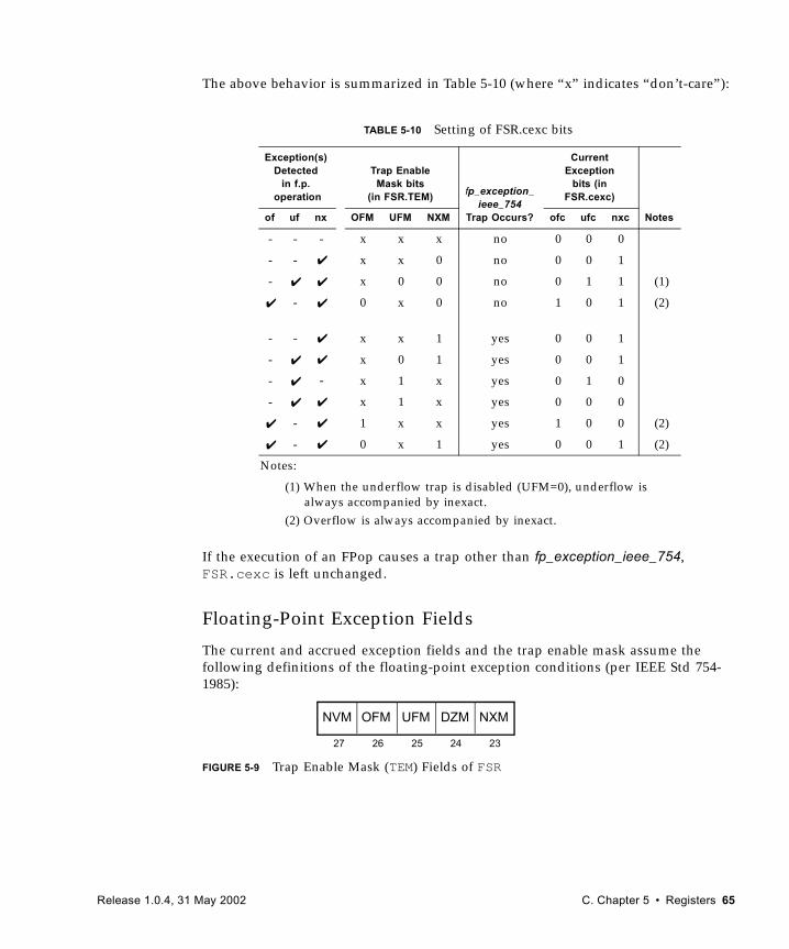
The above behavior is summarized in Table 5-10 (where “x” indicates “don’t-care”):
If the execution of an FPop causes a trap other than fp_exception_ieee_754, FSR.cexc is left unchanged.
Floating-Point Exception Fields
The current and accrued exception fields and the trap enable mask assume the following definitions of the floating-point exception conditions (per IEEE Std 754-1985):
FIGURE 5-9 Trap Enable Mask (TEM) Fields of FSR
TABLE 5-10 Setting of FSR.cexc bits
Exception(s)Detected
in f.p. operation
Trap EnableMask bits
(in FSR.TEM) fp_exception_ieee_754
Trap Occurs?
CurrentException
bits (inFSR.cexc)
of uf nx OFM UFM NXM ofc ufc nxc Notes
- - - x x x no 0 0 0
- - ✔ x x 0 no 0 0 1
- ✔ ✔ x 0 0 no 0 1 1 (1)
✔ - ✔ 0 x 0 no 1 0 1 (2)
- - ✔ x x 1 yes 0 0 1
- ✔ ✔ x 0 1 yes 0 0 1
- ✔ - x 1 x yes 0 1 0
- ✔ ✔ x 1 x yes 0 0 0
✔ - ✔ 1 x x yes 1 0 0 (2)
✔ - ✔ 0 x 1 yes 0 0 1 (2)
Notes:
(1) When the underflow trap is disabled (UFM=0), underflow is always accompanied by inexact.(2) Overflow is always accompanied by inexact.
24 2327 26 25
NVM OFM UFM DZM NXM
Release 1.0.4, 31 May 2002 C. Chapter 5 • Registers 65
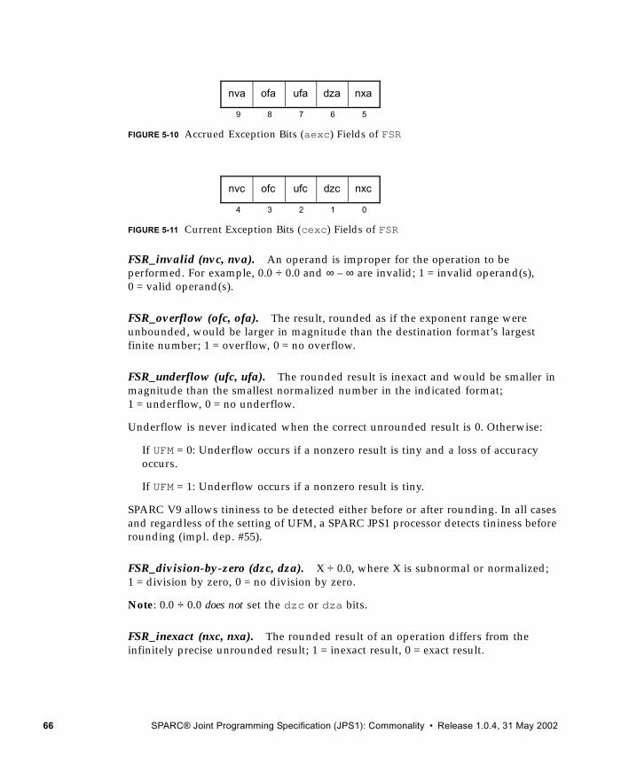
FIGURE 5-10 Accrued Exception Bits (aexc) Fields of FSR
FIGURE 5-11 Current Exception Bits (cexc) Fields of FSR
FSR_invalid (nvc, nva). An operand is improper for the operation to be performed. For example, 0.0 ÷ 0.0 and ∞ – ∞ are invalid; 1 = invalid operand(s), 0 = valid operand(s).
FSR_overflow (ofc, ofa). The result, rounded as if the exponent range were unbounded, would be larger in magnitude than the destination format’s largest finite number; 1 = overflow, 0 = no overflow.
FSR_underflow (ufc, ufa). The rounded result is inexact and would be smaller in magnitude than the smallest normalized number in the indicated format; 1 = underflow, 0 = no underflow.
Underflow is never indicated when the correct unrounded result is 0. Otherwise:
If UFM = 0: Underflow occurs if a nonzero result is tiny and a loss of accuracy occurs.
If UFM = 1: Underflow occurs if a nonzero result is tiny.
SPARC V9 allows tininess to be detected either before or after rounding. In all cases and regardless of the setting of UFM, a SPARC JPS1 processor detects tininess before rounding (impl. dep. #55).
FSR_division-by-zero (dzc, dza). X ÷ 0.0, where X is subnormal or normalized; 1 = division by zero, 0 = no division by zero.
Note: 0.0 ÷ 0.0 does not set the dzc or dza bits.
FSR_inexact (nxc, nxa). The rounded result of an operation differs from the infinitely precise unrounded result; 1 = inexact result, 0 = exact result.
6 59 8 7
nva ofa ufa dza nxa
1 04 3 2
nvc ofc ufc dzc nxc
66 SPARC® Joint Programming Specification (JPS1): Commonality • Release 1.0.4, 31 May 2002
Programming Note – Software must be capable of simulating the operation of the FPU in order to properly handle the unimplemented_FPop, unfinished_FPop, and IEEE_754_exception floating-point trap types. Thus, a user application program always sees an FSR that is fully compliant with IEEE Std 754-1985.
FSR Conformance
IMPL. DEP. #22: An implementation may choose to implement the TEM, cexc, and aexc fields in hardware in either of two ways (both of which comply with IEEE Std 754-1985):
1. Implement all three fields conformant to IEEE Std 754-1985.
2. Implement the inexact (NXM, nxa, and nxc) bits of these fields conformant to IEEE Std 754-1985, plus implement each of the remaining bits in the three fields (for invalid, overflow, under, and division-by-zero conditions) either:
a. Conformant to IEEE Std 754-1985, or
b. as a state bit that may be set by software that calculates the IEEE Std 754-1985 value of the bit. For any bit implemented as a state bit:
i. The IEEE exception corresponding to the state bit must always cause an exception (specifically, an unfinished_FPop exception). During exception processing in the trap handler, the bit in the state field can be written to the appropriate value by an LDFSR or LDXFSR instruction.
ii. The state bit must be implemented in such a way that if it is written to a particular value by an LDFSR or LDXFSR instruction, it will be read back as the same value by a subsequent STFSR or STXFSR.
Programming Note – Privileged software (or a combination of privileged and nonprivileged software) must be capable of simulating the operation of the FPU in order to handle the unimplemented_FPop, unfinished_FPop, and IEEE_754_exception floating-point trap types properly. Thus, a user application program always sees an FSR that is fully compliant with IEEE Std 754-1985.
5.1.8 Address Space Identifier (ASI) Register The Address Space Identifier Register (FIGURE 5-12) specifies the address space identifier to be used for load and store alternate instructions that use the “rs1 + simm13” addressing form. Nonprivileged (user-mode) software may write any value into the ASI register; however, values with bit 7 = 0 indicate restricted ASIs.
Release 1.0.4, 31 May 2002 C. Chapter 5 • Registers 67
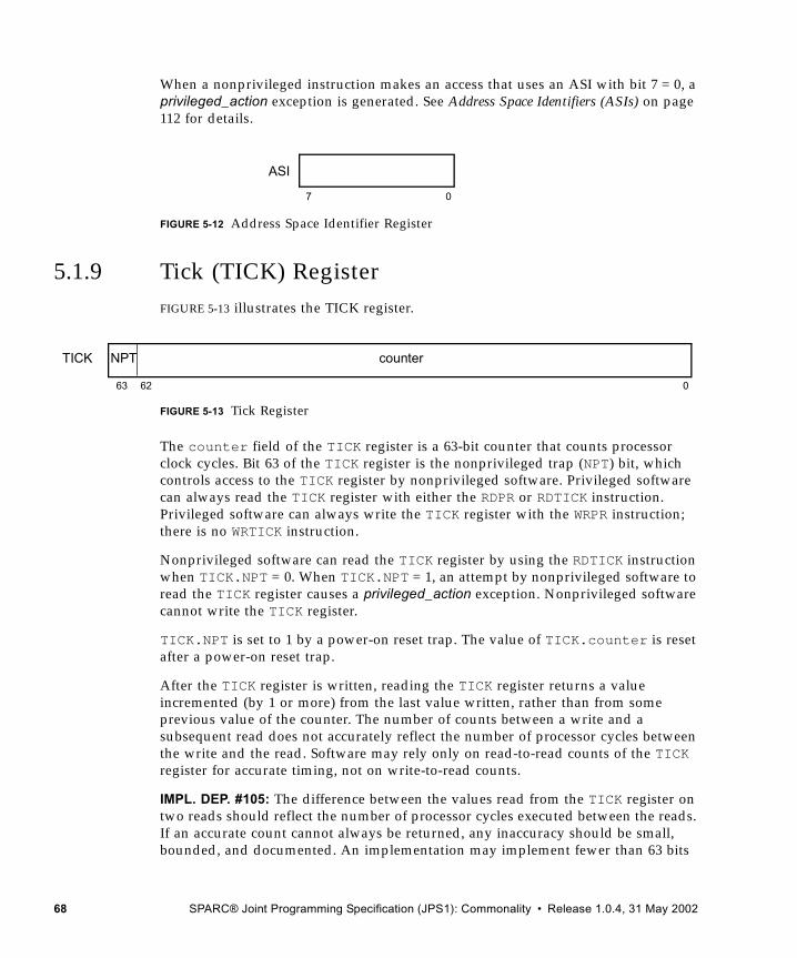
When a nonprivileged instruction makes an access that uses an ASI with bit 7 = 0, a privileged_action exception is generated. See Address Space Identifiers (ASIs) on page 112 for details.
FIGURE 5-12 Address Space Identifier Register
5.1.9 Tick (TICK) RegisterFIGURE 5-13 illustrates the TICK register.
FIGURE 5-13 Tick Register
The counter field of the TICK register is a 63-bit counter that counts processor clock cycles. Bit 63 of the TICK register is the nonprivileged trap (NPT) bit, which controls access to the TICK register by nonprivileged software. Privileged software can always read the TICK register with either the RDPR or RDTICK instruction. Privileged software can always write the TICK register with the WRPR instruction; there is no WRTICK instruction.
Nonprivileged software can read the TICK register by using the RDTICK instruction when TICK.NPT = 0. When TICK.NPT = 1, an attempt by nonprivileged software to read the TICK register causes a privileged_action exception. Nonprivileged software cannot write the TICK register.
TICK.NPT is set to 1 by a power-on reset trap. The value of TICK.counter is reset after a power-on reset trap.
After the TICK register is written, reading the TICK register returns a value incremented (by 1 or more) from the last value written, rather than from some previous value of the counter. The number of counts between a write and a subsequent read does not accurately reflect the number of processor cycles between the write and the read. Software may rely only on read-to-read counts of the TICK register for accurate timing, not on write-to-read counts.
IMPL. DEP. #105: The difference between the values read from the TICK register on two reads should reflect the number of processor cycles executed between the reads. If an accurate count cannot always be returned, any inaccuracy should be small, bounded, and documented. An implementation may implement fewer than 63 bits
7 0
ASI
063 62
TICK NPT counter
68 SPARC® Joint Programming Specification (JPS1): Commonality • Release 1.0.4, 31 May 2002
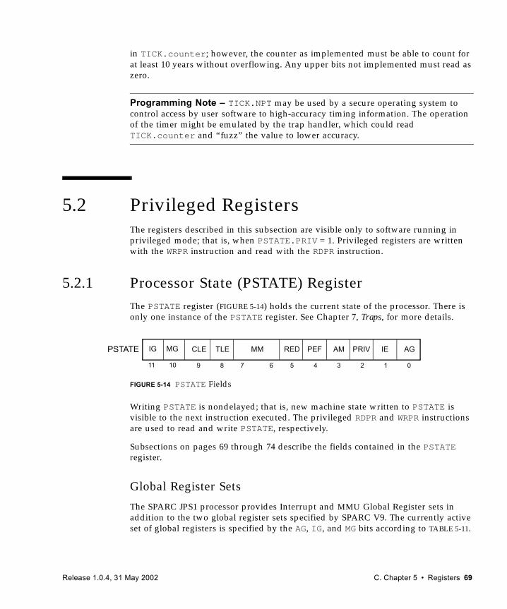
in TICK.counter; however, the counter as implemented must be able to count for at least 10 years without overflowing. Any upper bits not implemented must read as zero.
Programming Note – TICK.NPT may be used by a secure operating system to control access by user software to high-accuracy timing information. The operation of the timer might be emulated by the trap handler, which could read TICK.counter and “fuzz” the value to lower accuracy.
5.2 Privileged RegistersThe registers described in this subsection are visible only to software running in privileged mode; that is, when PSTATE.PRIV = 1. Privileged registers are written with the WRPR instruction and read with the RDPR instruction.
5.2.1 Processor State (PSTATE) RegisterThe PSTATE register (FIGURE 5-14) holds the current state of the processor. There is only one instance of the PSTATE register. See Chapter 7, Traps, for more details.
FIGURE 5-14 PSTATE Fields
Writing PSTATE is nondelayed; that is, new machine state written to PSTATE is visible to the next instruction executed. The privileged RDPR and WRPR instructions are used to read and write PSTATE, respectively.
Subsections on pages 69 through 74 describe the fields contained in the PSTATE register.
Global Register Sets
The SPARC JPS1 processor provides Interrupt and MMU Global Register sets in addition to the two global register sets specified by SPARC V9. The currently active set of global registers is specified by the AG, IG, and MG bits according to TABLE 5-11.
4 0
PSTATE PEF AM PRIV IE AG
3 2 16 5
MM RED
7
TLECLE
9 8
MGIG
1011
Release 1.0.4, 31 May 2002 C. Chapter 5 • Registers 69
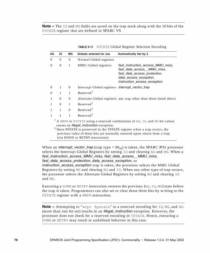
Note – The IG and MG fields are saved on the trap stack along with the 10 bits of the PSTATE register that are defined in SPARC V9.
When an interrupt_vector_trap (trap type = 6016) is taken, the SPARC JPS1 processor selects the Interrupt Global Registers by setting IG and clearing AG and MG. When a fast_instruction_access_MMU_miss, fast_data_access__MMU_miss, fast_data_access_protection, data_access_exception, or instruction_access_exception trap is taken, the processor selects the MMU Global Registers by setting MG and clearing AG and IG. When any other type of trap occurs, the processor selects the Alternate Global Registers by setting AG and clearing IG and MG.
Executing a DONE or RETRY instruction restores the previous {AG, IG, MG} state before the trap is taken. Programmers can also set or clear these three bits by writing to the PSTATE register with a WRPR instruction.
Note – Attempting to “wrpr %pstate” to a reserved encoding for IG, MG, and AG (more than one bit set) results in an illegal_instruction exception. However, the processor does not check for a reserved encoding in TSTATE. Hence, executing a DONE or RETRY may result in undefined behavior in this case.
TABLE 5-11 PSTATE Global Register Selection Encoding
AG IG MG Globals selected for use Automatically Set by ‡
0 0 0 Normal Global registers
0 0 1 MMU Global registers fast_instruction_access_MMU_miss,fast_data_access__MMU_miss,fast_data_access_protection,data_access_exception,instruction_access_exception
0 1 0 Interrupt Global registers interrupt_vector_trap
0 1 1 Reserved†
1 0 0 Alternate Global registers any trap other than those listed above
1 0 1 Reserved†
1 1 0 Reserved†
1 1 1 Reserved†
† A WRPR to PSTATE using a reserved combination of AG, IG, and MG bit values causes an illegal_instruction exception.‡ Since PSTATE is preserved in the TSTATE register when a trap occurs, the previous value of these bits are normally restored upon return from a trap (via DONE or RETRY instruction)
70 SPARC® Joint Programming Specification (JPS1): Commonality • Release 1.0.4, 31 May 2002
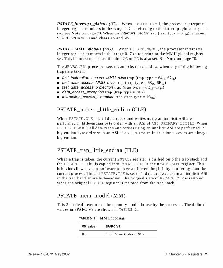
PSTATE_interrupt_globals (IG). When PSTATE.IG = 1, the processor interprets integer register numbers in the range 0–7 as referring to the interrupt global register set. See Note on page 70. When an interrupt_vector trap (trap type = 6016) is taken, SPARC V9 sets IG and clears AG and MG.
PSTATE_MMU_globals (MG). When PSTATE.MG = 1, the processor interprets integer register numbers in the range 0–7 as referring to the MMU global register set. This bit must not be set if either AG or IG is also set. See Note on page 70.
The SPARC JPS1 processor sets MG and clears IG and AG when any of the following traps are taken:
■ fast_instruction_access_MMU_miss trap (trap type = 6416–6716)■ fast_data_access_MMU_miss trap (trap type = 6816–6B16)■ fast_data_access_protection trap (trap type = 6C16–6F16)■ data_access_exception trap (trap type = 3016)■ instruction_access_exception trap (trap type = 0816)
PSTATE_current_little_endian (CLE)
When PSTATE.CLE = 1, all data reads and writes using an implicit ASI are performed in little-endian byte order with an ASI of ASI_PRIMARY_LITTLE. When PSTATE.CLE = 0, all data reads and writes using an implicit ASI are performed in big-endian byte order with an ASI of ASI_PRIMARY. Instruction accesses are always big-endian.
PSTATE_trap_little_endian (TLE)
When a trap is taken, the current PSTATE register is pushed onto the trap stack and the PSTATE.TLE bit is copied into PSTATE.CLE in the new PSTATE register. This behavior allows system software to have a different implicit byte ordering than the current process. Thus, if PSTATE.TLE is set to 1, data accesses using an implicit ASI in the trap handler are little-endian. The original state of PSTATE.CLE is restored when the original PSTATE register is restored from the trap stack.
PSTATE_mem_model (MM)
This 2-bit field determines the memory model in use by the processor. The defined values in SPARC V9 are shown in TABLE 5-12.
TABLE 5-12 MM Encodings
MM Value SPARC V9
00 Total Store Order (TSO)
Release 1.0.4, 31 May 2002 C. Chapter 5 • Registers 71
The current memory model is determined by the value of PSTATE.MM. Software should always refrain from using the combination 11 because it is reserved for future SPARC V9 extensions.
■ Total Store Order (TSO) — Loads are ordered with respect to earlier loads. Stores are ordered with respect to earlier loads and stores. Thus, loads can bypass earlier stores but cannot bypass earlier loads; stores cannot bypass earlier loads and stores. Programs that execute correctly in either PSO or RMO will execute correctly in the TSO model.
■ Partial Store Order (PSO) — Loads and stores ordered with respect to earlier loads; atomic load-stores are ordered with respect to loads. Explicit MEMBAR instructions are required to order store and atomic load-store instructions with respect to each other.
■ Relaxed Memory Order (RMO) — Hardware can schedule memory accesses in any order, as long as the program computes the correct result. In other words, RMO places no ordering constraints on memory references beyond those required for processor self-consistency. When ordering is required, it must be provided explicitly in the programs by MEMBAR instructions.
IMPL. DEP. #113: Whether the PSO or RMO models are supported by SPARC V9 systems is implementation dependent.
IMPL. DEP. #119: The effect of writing an unimplemented memory mode designation into PSTATE.MM is implementation dependent.
PSTATE_RED_state (RED)
PSTATE.RED (Reset, Error, and Debug state) is set whenever the SPARC JPS1 processor takes a RED state disrupting or nondisrupting trap. See RED_state on page 133. The IU sets PSTATE.RED when any hardware reset occurs. It also sets PSTATE.RED when a trap is taken while TL = (MAXTL − 1). Software can exit RED_state by one of two methods:
1. Execute a DONE or RETRY instruction, which restores the stacked copy of PSTATE and clears PSTATE.RED if it was 0 in the stacked copy.
2. Write a 0 to PSTATE.RED with a WRPR instruction.
01 Partial Store Order (PSO)
10 Relaxed Memory Order (RMO)
11 Reserved
TABLE 5-12 MM Encodings
MM Value SPARC V9
72 SPARC® Joint Programming Specification (JPS1): Commonality • Release 1.0.4, 31 May 2002
Programming Note – Changing PSTATE.RED may cause a change in address mapping on some systems. It is recommended that writes of PSTATE.RED be placed in the delay slot of a JMPL; the target of this JMPL should be in the new address mapping. The JMPL sets the nPC, which becomes the PC for the instruction that follows the 'WRPR' in its delay slot. The effect of the WRPR instruction is immediate.
PSTATE_enable_floating-point (PEF)
When set to 1, the PEF bit enables the floating-point unit, which allows privileged software to manage the FPU. For the FPU to be usable, both PSTATE.PEF and FPRS.FEF must be set. Otherwise, any floating-point instruction (including the future JPS-specific multiply-add and multiply-subtract instructions) that tries to reference the FPU causes an fp_disabled trap.
PSTATE_address_mask (AM)
When PSTATE.AM = 1, the high-order 32 bits of all instruction and data addresses are set to 0 in the following cases:
■ Before data addresses are sent out of the processor
■ For instruction accesses to caches (both internal and external)
■ Before being stored to a general-purpose register for CALL, JMPL, and RDPC instructions (impl. dep. #125; see below)
■ Before being stored to TPC[n] and TNPC[n] when a trap occurs (impl. dep. #125; see specific SPARC JPS1 Implementation Supplements)
When an ASI_PHYS_* ASI is used in a load or store instruction, the setting of PSTATE.AM is ignored and the full 64-bit address is used. (See ASI 1416, ASI_PHYS_USE_EC, for an example.)
IMPL. DEP. #125: When PSTATE.AM = 1, the value of the high-order 32-bits of the PC transmitted to the specified destination register(s) by CALL, JMPL, RDPC, and saved during a trap is implementation dependent.
IMPL. DEP. #241: When PSTATE.AM = 1 and an exception occurs, the value written to the more-significant 32 bits of the Data Synchronous Fault Address Register (DSFAR) is implementation dependent.
The PSTATE.AM bit must be set when 32-bit software is executed.
PSTATE_privileged_mode (PRIV)
When PSTATE.PRIV = 1, the processor is in privileged mode.
Release 1.0.4, 31 May 2002 C. Chapter 5 • Registers 73
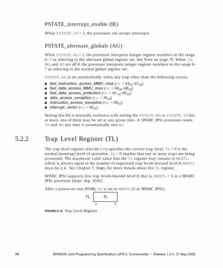
PSTATE_interrupt_enable (IE)
When PSTATE.IE = 1, the processor can accept interrupts.
PSTATE_alternate_globals (AG)
When PSTATE.AG = 1, the processor interprets integer register numbers in the range 0–7 as referring to the alternate global register set. See Note on page 70. When IG, MG, and AG are all 0, the processor interprets integer register numbers in the range 0–7 as referring to the normal global register set.
PSTATE.AG is set automatically when any trap other than the following occurs:
■ fast_instruction_access_MMU_miss (tt = 6416–6716)■ fast_data_access_MMU_miss (tt = 6816–6B16)■ fast_data_access_protection (tt = 6C16–6F16)■ data_access_exception (tt = 3016)■ instruction_access_exception (tt = 0816)■ interrupt_vector (tt = 6016)
Setting this bit is mutually exclusive with setting the PSTATE.MG or PSTATE.IG bit; at most, one of them may be set at any given time. A SPARC JPS1 processor resets IG and MG any time it automatically sets AG.
5.2.2 Trap Level Register (TL)The trap level register (FIGURE 5-15) specifies the current trap level. TL = 0 is the normal (nontrap) level of operation. TL > 0 implies that one or more traps are being processed. The maximum valid value that the TL register may contain is MAXTL, which is always equal to the number of supported trap levels beyond level 0; MAXTL must be ≥ 4. See Chapter 7, Traps, for more details about the TL register.
SPARC JPS1 supports five trap levels beyond level 0; that is, MAXTL = 5 in a SPARC JPS1 processor (impl. dep. #101).
After a power-on rest (POR), TL is set to MAXTL (5 in SPARC JPS1).
FIGURE 5-15 Trap Level Register
2 0
TL TL
74 SPARC® Joint Programming Specification (JPS1): Commonality • Release 1.0.4, 31 May 2002
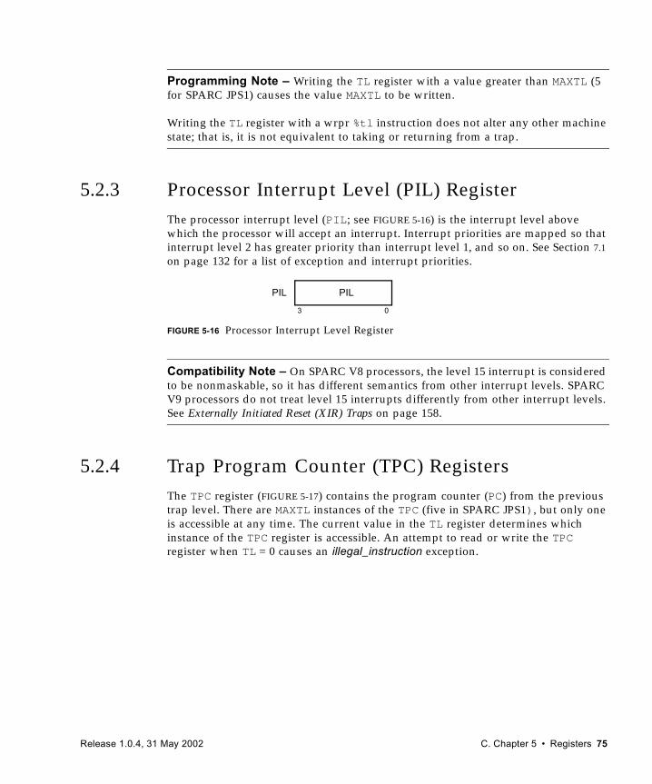
Programming Note – Writing the TL register with a value greater than MAXTL (5 for SPARC JPS1) causes the value MAXTL to be written.
Writing the TL register with a wrpr %tl instruction does not alter any other machine state; that is, it is not equivalent to taking or returning from a trap.
5.2.3 Processor Interrupt Level (PIL) RegisterThe processor interrupt level (PIL; see FIGURE 5-16) is the interrupt level above which the processor will accept an interrupt. Interrupt priorities are mapped so that interrupt level 2 has greater priority than interrupt level 1, and so on. See Section 7.1 on page 132 for a list of exception and interrupt priorities.
FIGURE 5-16 Processor Interrupt Level Register
Compatibility Note – On SPARC V8 processors, the level 15 interrupt is considered to be nonmaskable, so it has different semantics from other interrupt levels. SPARC V9 processors do not treat level 15 interrupts differently from other interrupt levels. See Externally Initiated Reset (XIR) Traps on page 158.
5.2.4 Trap Program Counter (TPC) RegistersThe TPC register (FIGURE 5-17) contains the program counter (PC) from the previous trap level. There are MAXTL instances of the TPC (five in SPARC JPS1), but only one is accessible at any time. The current value in the TL register determines which instance of the TPC register is accessible. An attempt to read or write the TPC register when TL = 0 causes an illegal_instruction exception.
3 0
PIL PIL
Release 1.0.4, 31 May 2002 C. Chapter 5 • Registers 75
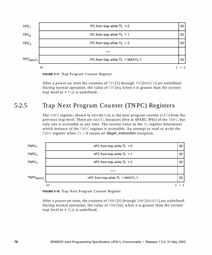
After a power-on reset the contents of TPC[1] through TPC[MAXTL] are undefined. During normal operation, the value of TPC[n], when n is greater than the current trap level (n > TL), is undefined.
5.2.5 Trap Next Program Counter (TNPC) RegistersThe TNPC register, shown in FIGURE 5-18, is the next program counter (nPC) from the previous trap level. There are MAXTL instances (five in SPARC JPS1) of the TNPC, but only one is accessible at any time. The current value in the TL register determines which instance of the TNPC register is accessible. An attempt to read or write the TNPC register when TL = 0 causes an illegal_instruction exception.
FIGURE 5-18 Trap Next Program Counter Register
After a power-on reset, the contents of TNPC[1] through TNPC[MAXTL] are undefined. During normal operation, the value of TNPC[n], when n is greater than the current trap level (n > TL), is undefined.
TPC1 PC from trap while TL = 0
2
00
63 1 0
TPC2 PC from trap while TL = 1 00
TPC3 PC from trap while TL = 2 00
…
PC from trap while TL = MAXTL-1 00TPCMAXTL
FIGURE 5-17 Trap Program Counter Register
TNPC1 nPC from trap while TL = 0
2
00
63 1 0
TNPC2 nPC from trap while TL = 1 00
TNPC3 nPC from trap while TL = 2 00
…
nPC from trap while TL = MAXTL-1 00TNPCMAXTL
76 SPARC® Joint Programming Specification (JPS1): Commonality • Release 1.0.4, 31 May 2002
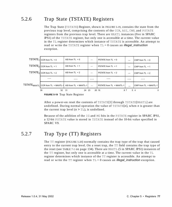
5.2.6 Trap State (TSTATE) Registers
The Trap State (TSTATE) Register, shown in FIGURE 5-19, contains the state from the previous trap level, comprising the contents of the CCR, ASI, CWP, and PSTATE registers from the previous trap level. There are MAXTL instances (five in SPARC JPS1) of the TSTATE register, but only one is accessible at a time. The current value in the TL register determines which instance of TSTATE is accessible. An attempt to read or write the TSTATE register when TL = 0 causes an illegal_instruction exception.
FIGURE 5-19 Trap State Register
After a power-on reset the contents of TSTATE[1] through TSTATE[MAXTL] are undefined. During normal operation the value of TSTATE[n], when n is greater than the current trap level (n > TL), is undefined.
Because of the addition of the IG and MG bits in the PSTATE register in SPARC JPS1, a 12-bit PSTATE value is stored in TSTATE instead of the 10-bit value specified in SPARC V9.
5.2.7 Trap Type (TT) Registers The TT register (FIGURE 5-20) normally contains the trap type of the trap that caused entry to the current trap level. On a reset trap, the TT field contains the trap type of the reset (see TABLE 7-1 on page 134). There are MAXTL (5 in SPARC JPS1) instances of the TT register, but only one is accessible at a time. The current value in the TL register determines which instance of the TT register is accessible. An attempt to read or write the TT register when TL = 0 causes an illegal_instruction exception.
39 0
TSTATE1 CCR from TL = 0 CWP from TL = 0ASI from TL = 0 PSTATE from TL = 0— —
432 31 24 23 20 8 7 519
TSTATE2 CCR from TL = 1 CWP from TL = 1ASI from TL = 1 PSTATE from TL = 1— —
TSTATE3 CCR from TL = 2 CWP from TL = 2ASI from TL = 2 PSTATE from TL = 2— —
…
TSTATEMAXTL CCR from TL = MAXTL-1 CWP from TL = MAXTL-1ASI from TL = MAXTL-1 PSTATE from TL = MAXTL-1— —
… … …… …
Release 1.0.4, 31 May 2002 C. Chapter 5 • Registers 77
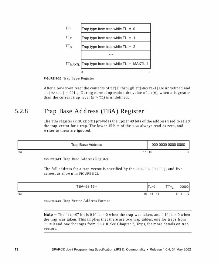
FIGURE 5-20 Trap Type Register
After a power-on reset the contents of TT[1] through TT[MAXTL-1] are undefined and TT[MAXTL] = 00116. During normal operation the value of TT[n], when n is greater than the current trap level (n > TL) is undefined.
5.2.8 Trap Base Address (TBA) RegisterThe TBA register (FIGURE 5-21) provides the upper 49 bits of the address used to select the trap vector for a trap. The lower 15 bits of the TBA always read as zero, and writes to them are ignored.
FIGURE 5-21 Trap Base Address Register
The full address for a trap vector is specified by the TBA, TL, TT[TL], and five zeroes, as shown in FIGURE 5-22.
FIGURE 5-22 Trap Vector Address Format
Note – The “TL>0” bit is 0 if TL = 0 when the trap was taken, and 1 if TL > 0 when the trap was taken. This implies that there are two trap tables: one for traps from TL = 0 and one for traps from TL > 0. See Chapter 7, Traps, for more details on trap vectors.
TT1 Trap type from trap while TL = 0
8 0
TT2 Trap type from trap while TL = 1
TT3 Trap type from trap while TL = 2
…
TTMAXTL Trap type from trap while TL = MAXTL-1
63 15 14 0
000 0000 0000 0000Trap Base Address
63 15 14 0
TBA<63:15>
13 45
TL>0 TTTL 00000
78 SPARC® Joint Programming Specification (JPS1): Commonality • Release 1.0.4, 31 May 2002
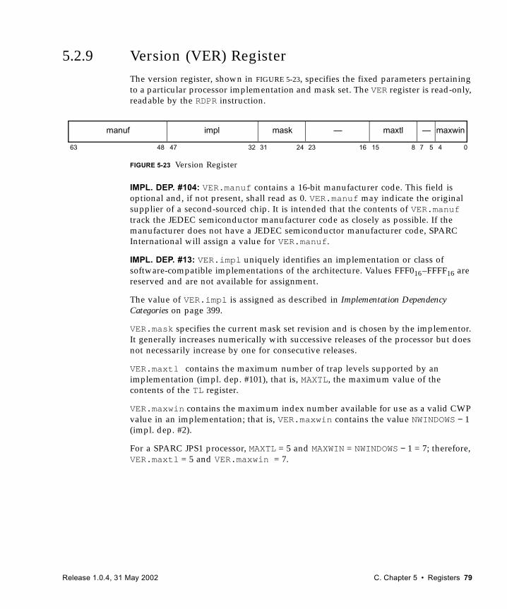
5.2.9 Version (VER) RegisterThe version register, shown in FIGURE 5-23, specifies the fixed parameters pertaining to a particular processor implementation and mask set. The VER register is read-only, readable by the RDPR instruction.
FIGURE 5-23 Version Register
IMPL. DEP. #104: VER.manuf contains a 16-bit manufacturer code. This field is optional and, if not present, shall read as 0. VER.manuf may indicate the original supplier of a second-sourced chip. It is intended that the contents of VER.manuf track the JEDEC semiconductor manufacturer code as closely as possible. If the manufacturer does not have a JEDEC semiconductor manufacturer code, SPARC International will assign a value for VER.manuf.
IMPL. DEP. #13: VER.impl uniquely identifies an implementation or class of software-compatible implementations of the architecture. Values FFF016–FFFF16 are reserved and are not available for assignment.
The value of VER.impl is assigned as described in Implementation Dependency Categories on page 399.
VER.mask specifies the current mask set revision and is chosen by the implementor. It generally increases numerically with successive releases of the processor but does not necessarily increase by one for consecutive releases.
VER.maxtl contains the maximum number of trap levels supported by an implementation (impl. dep. #101), that is, MAXTL, the maximum value of the contents of the TL register.
VER.maxwin contains the maximum index number available for use as a valid CWP value in an implementation; that is, VER.maxwin contains the value NWINDOWS − 1 (impl. dep. #2).
For a SPARC JPS1 processor, MAXTL = 5 and MAXWIN = NWINDOWS − 1 = 7; therefore, VER.maxtl = 5 and VER.maxwin = 7.
63 48 47 24 23 16 15 8 7 05 432 31
maxwin—maxtl—maskimplmanuf
Release 1.0.4, 31 May 2002 C. Chapter 5 • Registers 79
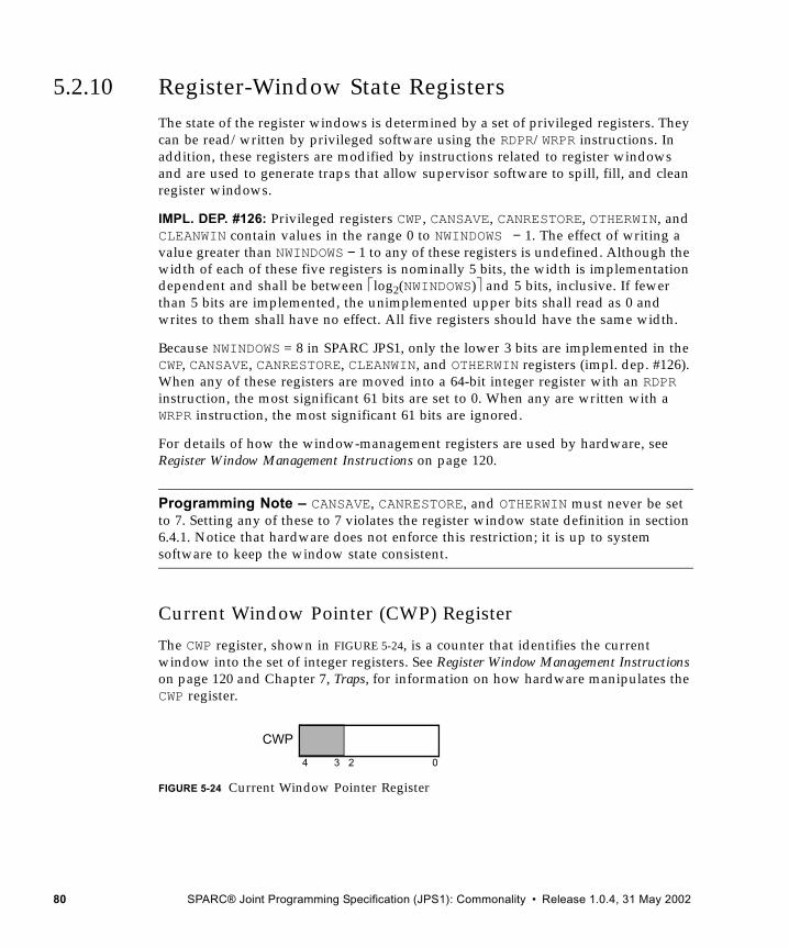
5.2.10 Register-Window State RegistersThe state of the register windows is determined by a set of privileged registers. They can be read/written by privileged software using the RDPR/WRPR instructions. In addition, these registers are modified by instructions related to register windows and are used to generate traps that allow supervisor software to spill, fill, and clean register windows.
IMPL. DEP. #126: Privileged registers CWP, CANSAVE, CANRESTORE, OTHERWIN, and CLEANWIN contain values in the range 0 to NWINDOWS − 1. The effect of writing a value greater than NWINDOWS − 1 to any of these registers is undefined. Although the width of each of these five registers is nominally 5 bits, the width is implementation dependent and shall be between log2(NWINDOWS) and 5 bits, inclusive. If fewer than 5 bits are implemented, the unimplemented upper bits shall read as 0 and writes to them shall have no effect. All five registers should have the same width.
Because NWINDOWS = 8 in SPARC JPS1, only the lower 3 bits are implemented in the CWP, CANSAVE, CANRESTORE, CLEANWIN, and OTHERWIN registers (impl. dep. #126). When any of these registers are moved into a 64-bit integer register with an RDPR instruction, the most significant 61 bits are set to 0. When any are written with a WRPR instruction, the most significant 61 bits are ignored.
For details of how the window-management registers are used by hardware, see Register Window Management Instructions on page 120.
Programming Note – CANSAVE, CANRESTORE, and OTHERWIN must never be set to 7. Setting any of these to 7 violates the register window state definition in section 6.4.1. Notice that hardware does not enforce this restriction; it is up to system software to keep the window state consistent.
Current Window Pointer (CWP) Register
The CWP register, shown in FIGURE 5-24, is a counter that identifies the current window into the set of integer registers. See Register Window Management Instructions on page 120 and Chapter 7, Traps, for information on how hardware manipulates the CWP register.
FIGURE 5-24 Current Window Pointer Register
4 0
CWP
3 2
80 SPARC® Joint Programming Specification (JPS1): Commonality • Release 1.0.4, 31 May 2002
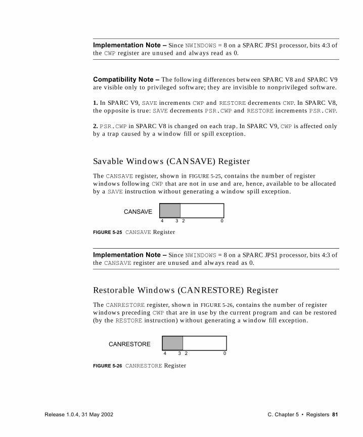
Implementation Note – Since NWINDOWS = 8 on a SPARC JPS1 processor, bits 4:3 of the CWP register are unused and always read as 0.
Compatibility Note – The following differences between SPARC V8 and SPARC V9 are visible only to privileged software; they are invisible to nonprivileged software.
1. In SPARC V9, SAVE increments CWP and RESTORE decrements CWP. In SPARC V8, the opposite is true: SAVE decrements PSR.CWP and RESTORE increments PSR.CWP.
2. PSR.CWP in SPARC V8 is changed on each trap. In SPARC V9, CWP is affected only by a trap caused by a window fill or spill exception.
Savable Windows (CANSAVE) Register
The CANSAVE register, shown in FIGURE 5-25, contains the number of register windows following CWP that are not in use and are, hence, available to be allocated by a SAVE instruction without generating a window spill exception.
FIGURE 5-25 CANSAVE Register
Implementation Note – Since NWINDOWS = 8 on a SPARC JPS1 processor, bits 4:3 of the CANSAVE register are unused and always read as 0.
Restorable Windows (CANRESTORE) Register
The CANRESTORE register, shown in FIGURE 5-26, contains the number of register windows preceding CWP that are in use by the current program and can be restored (by the RESTORE instruction) without generating a window fill exception.
FIGURE 5-26 CANRESTORE Register
CANSAVE4 03 2
CANRESTORE4 03 2
Release 1.0.4, 31 May 2002 C. Chapter 5 • Registers 81
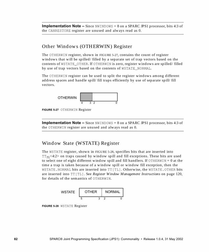
Implementation Note – Since NWINDOWS = 8 on a SPARC JPS1 processor, bits 4:3 of the CANRESTORE register are unused and always read as 0.
Other Windows (OTHERWIN) Register
The OTHERWIN register, shown in FIGURE 5-27, contains the count of register windows that will be spilled/filled by a separate set of trap vectors based on the contents of WSTATE_OTHER. If OTHERWIN is zero, register windows are spilled/filled by use of trap vectors based on the contents of WSTATE_NORMAL.
The OTHERWIN register can be used to split the register windows among different address spaces and handle spill/fill traps efficiently by use of separate spill/fill vectors.
FIGURE 5-27 OTHERWIN Register
Implementation Note – Since NWINDOWS = 8 on a SPARC JPS1 processor, bits 4:3 of the OTHERWIN register are unused and always read as 0.
Window State (WSTATE) Register
The WSTATE register, shown in FIGURE 5-28, specifies bits that are inserted into TTTL<4:2> on traps caused by window spill and fill exceptions. These bits are used to select one of eight different window spill and fill handlers. If OTHERWIN = 0 at the time a trap is taken because of a window spill or window fill exception, then the WSTATE.NORMAL bits are inserted into TT[TL]. Otherwise, the WSTATE.OTHER bits are inserted into TT[TL]. See Register Window Management Instructions on page 120, for details of the semantics of OTHERWIN.
FIGURE 5-28 WSTATE Register
OTHERWIN4 03 2
WSTATE
05 3 2
OTHER NORMAL
82 SPARC® Joint Programming Specification (JPS1): Commonality • Release 1.0.4, 31 May 2002
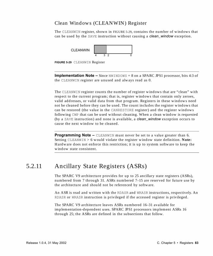
Clean Windows (CLEANWIN) Register
The CLEANWIN register, shown in FIGURE 5-29, contains the number of windows that can be used by the SAVE instruction without causing a clean_window exception.
FIGURE 5-29 CLEANWIN Register
Implementation Note – Since NWINDOWS = 8 on a SPARC JPS1 processor, bits 4:3 of the CLEANWIN register are unused and always read as 0.
The CLEANWIN register counts the number of register windows that are “clean” with respect to the current program; that is, register windows that contain only zeroes, valid addresses, or valid data from that program. Registers in these windows need not be cleaned before they can be used. The count includes the register windows that can be restored (the value in the CANRESTORE register) and the register windows following CWP that can be used without cleaning. When a clean window is requested (by a SAVE instruction) and none is available, a clean_window exception occurs to cause the next window to be cleaned.
Programming Note – CLEANWIN must never be set to a value greater than 6. Setting CLEANWIN > 6 would violate the register window state definition. Note: Hardware does not enforce this restriction; it is up to system software to keep the window state consistent.
5.2.11 Ancillary State Registers (ASRs)The SPARC V9 architecture provides for up to 25 ancillary state registers (ASRs), numbered from 7 through 31. ASRs numbered 7–15 are reserved for future use by the architecture and should not be referenced by software.
An ASR is read and written with the RDASR and WRASR instructions, respectively. An RDASR or WRASR instruction is privileged if the accessed register is privileged.
The SPARC V9 architecture leaves ASRs numbered 16–31 available for implementation-dependent uses. SPARC JPS1 processors implement ASRs 16 through 25; the ASRs are defined in the subsections that follow.
CLEANWIN4 03 2
Release 1.0.4, 31 May 2002 C. Chapter 5 • Registers 83
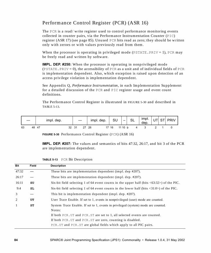
Performance Control Register (PCR) (ASR 16)
The PCR is a read/write register used to control performance monitoring events collected in counter pairs, via the Performance Instrumentation Counter (PIC) register (ASR 17) (see page 85). Unused PCR bits read as zero; they should be written only with zeroes or with values previously read from them.
When the processor is operating in privileged mode (PSTATE.PRIV = 1), PCR may be freely read and written by software.
IMPL. DEP. #250: When the processor is operating in nonprivileged mode (PSTATE.PRIV = 0), the accessibility of PCR as a unit and of individual fields of PCR is implementation dependent. Also, which exception is raised upon detection of an access privilege violation is implementation dependent.
See Appendix Q, Performance Instrumentation, in each Implementation Supplement for a detailed discussion of the PCR and PIC register usage and event count definitions.
The Performance Control Register is illustrated in FIGURE 5-30 and described in TABLE 5-13.
FIGURE 5-30 Performance Control Register (PCR) (ASR 16)
IMPL. DEP. #207: The values and semantics of bits 47:32, 26:17, and bit 3 of the PCR are implementation dependent.
TABLE 5-13 PCR Bit Description
Bit Field Description
47:32 — These bits are implementation dependent (impl. dep #207).
26:17 — These bits are implementation dependent (impl. dep. #207).
16:11 SU Six-bit field selecting 1 of 64 event counts in the upper half (bits <63:32>) of the PIC.
9:4 SL Six-bit field selecting 1 of 64 event counts in the lower half (bits <31:0>) of the PIC.
3 — This bit is implementation dependent (impl. dep. #207).
2 UT User Trace Enable. If set to 1, events in nonprivileged (user) mode are counted.
1 ST System Trace Enable. If set to 1, events in privileged (system) mode are counted.
Notes: If both PCR.UT and PCR.ST are set to 1, all selected events are counted. If both PCR.UT and PCR.ST are zero, counting is disabled.PCR.UT and PCR.ST are global fields which apply to all PIC pairs.
63 16 11 10 9 4 0
– SLSU
174748
— UT ST PRIV
123
impl. dep. impl.dep.
impl. dep.
3132 27 26
—
84 SPARC® Joint Programming Specification (JPS1): Commonality • Release 1.0.4, 31 May 2002
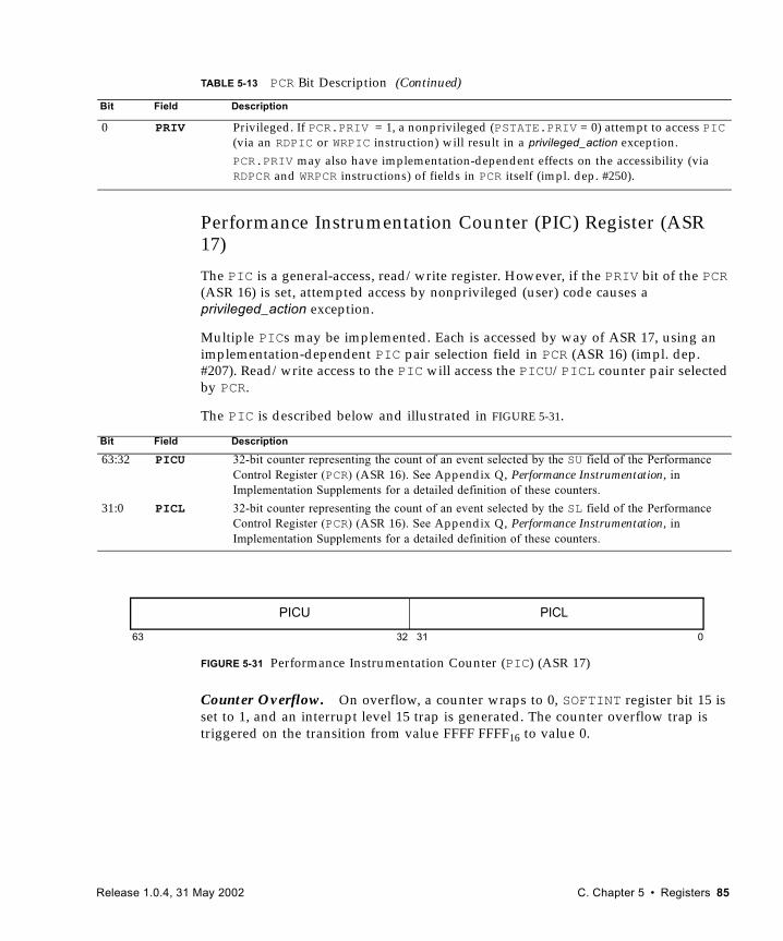
Performance Instrumentation Counter (PIC) Register (ASR 17)
The PIC is a general-access, read/write register. However, if the PRIV bit of the PCR (ASR 16) is set, attempted access by nonprivileged (user) code causes a privileged_action exception.
Multiple PICs may be implemented. Each is accessed by way of ASR 17, using an implementation-dependent PIC pair selection field in PCR (ASR 16) (impl. dep. #207). Read/write access to the PIC will access the PICU/PICL counter pair selected by PCR.
The PIC is described below and illustrated in FIGURE 5-31.
FIGURE 5-31 Performance Instrumentation Counter (PIC) (ASR 17)
Counter Overflow. On overflow, a counter wraps to 0, SOFTINT register bit 15 is set to 1, and an interrupt level 15 trap is generated. The counter overflow trap is triggered on the transition from value FFFF FFFF16 to value 0.
0 PRIV Privileged. If PCR.PRIV = 1, a nonprivileged (PSTATE.PRIV = 0) attempt to access PIC (via an RDPIC or WRPIC instruction) will result in a privileged_action exception.PCR.PRIV may also have implementation-dependent effects on the accessibility (via RDPCR and WRPCR instructions) of fields in PCR itself (impl. dep. #250).
Bit Field Description
63:32 PICU 32-bit counter representing the count of an event selected by the SU field of the Performance Control Register (PCR) (ASR 16). See Appendix Q, Performance Instrumentation, in Implementation Supplements for a detailed definition of these counters.
31:0 PICL 32-bit counter representing the count of an event selected by the SL field of the Performance Control Register (PCR) (ASR 16). See Appendix Q, Performance Instrumentation, in Implementation Supplements for a detailed definition of these counters.
TABLE 5-13 PCR Bit Description (Continued)
Bit Field Description
063 3132
PICU PICL
Release 1.0.4, 31 May 2002 C. Chapter 5 • Registers 85
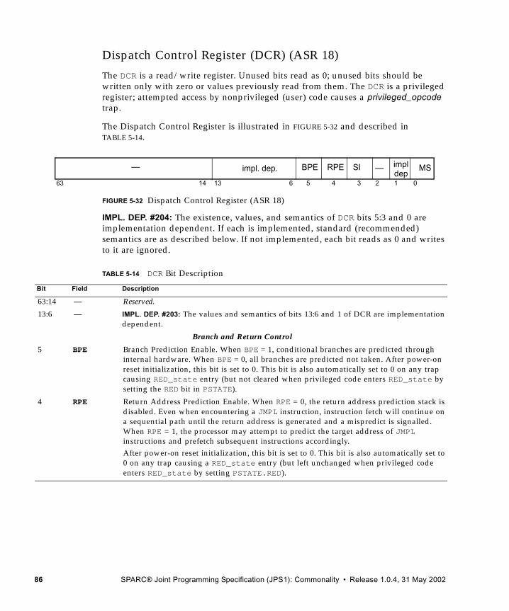
Dispatch Control Register (DCR) (ASR 18)
The DCR is a read/write register. Unused bits read as 0; unused bits should be written only with zero or values previously read from them. The DCR is a privileged register; attempted access by nonprivileged (user) code causes a privileged_opcode trap.
The Dispatch Control Register is illustrated in FIGURE 5-32 and described in TABLE 5-14.
FIGURE 5-32 Dispatch Control Register (ASR 18)
IMPL. DEP. #204: The existence, values, and semantics of DCR bits 5:3 and 0 are implementation dependent. If each is implemented, standard (recommended) semantics are as described below. If not implemented, each bit reads as 0 and writes to it are ignored.
TABLE 5-14 DCR Bit Description
Bit Field Description
63:14 — Reserved.
13:6 — IMPL. DEP. #203: The values and semantics of bits 13:6 and 1 of DCR are implementation dependent.
Branch and Return Control
5 BPE Branch Prediction Enable. When BPE = 1, conditional branches are predicted through internal hardware. When BPE = 0, all branches are predicted not taken. After power-on reset initialization, this bit is set to 0. This bit is also automatically set to 0 on any trap causing RED_state entry (but not cleared when privileged code enters RED_state by setting the RED bit in PSTATE).
4 RPE Return Address Prediction Enable. When RPE = 0, the return address prediction stack is disabled. Even when encountering a JMPL instruction, instruction fetch will continue on a sequential path until the return address is generated and a mispredict is signalled. When RPE = 1, the processor may attempt to predict the target address of JMPL instructions and prefetch subsequent instructions accordingly.After power-on reset initialization, this bit is set to 0. This bit is also automatically set to 0 on any trap causing a RED_state entry (but left unchanged when privileged code enters RED_state by setting PSTATE.RED).
0
—
63 1
MSSI
26
—RPEBPE
3451314
impl. dep. impldep
86 SPARC® Joint Programming Specification (JPS1): Commonality • Release 1.0.4, 31 May 2002
Graphics Status Register (GSR) (ASR 19)
The Graphics Status Register is a nonprivileged read/write registerimplicitly referenced by many VIS instructions1. The GSR can be read through RDGSR (see A.51 on page 313) and written through WRGSR (see A.70 on page 350).
The GSR is illustrated in FIGURE 5-33 and described in TABLE 5-15.
FIGURE 5-33 Graphic Status Register (GSR) (ASR 19)
Instruction Dispatch Control
3 SI Single Issue Disable. When SI = 0, only one instruction will be outstanding at a time. Superscalar instruction dispatch is disabled, and only one instruction is executed at a time. When SI = 1, normal pipelining is enabled. The processor can issue new instructions prior to the completion of previously issued instructions. After power-on reset initialization, this bit is set to 0. This bit is also automatically zeroed on any trap causing RED_state entry (but left unchanged when privileged code enters RED_state by setting PSTATE.RED).
2 — Reserved.
1 — IMPL. DEP. #203: The values and semantics of bits 13:6 and 1 of DCR are implementation dependent.
0 MS Multiscalar Dispatch Enable. When MS = 0, the processor operates in scalar mode, issuing and executing one instruction at a time. Pipelined operation is still controlled by the SI bit. MS = 1 enables superscalar (normal) instruction issue.After power-on reset initialization, this bit is set to 0. The bit is also zeroed automatically on any trap causing RED_state entry (but left unchanged when privileged code enters RED_state by setting PSTATE.RED).
1. Sun Microsystems’ “Visual Instruction Set”
TABLE 5-15 GSR Bit Description
Bit Field Description
63:32 MASK<31:0> This field specifies the mask used by the BSHUFFLE instruction. The field contents are set by the BMASK instruction.
31:28 Reserved27 IM Interval Mode: When IM = 1, the values in FSR.RD and FSR.NS are ignored; the
processor operates as if FSR.NS = 0 and rounds floating-point results according to GSR.IRND.
TABLE 5-14 DCR Bit Description (Continued)
Bit Field Description
0
—63 2325 24 8 7
SCALE ALIGNIRNDIMMASK
27283132 26
—
Release 1.0.4, 31 May 2002 C. Chapter 5 • Registers 87
Accesses to the Graphics Status Register cause an fp_disabled trap if PSTATE.PEF or FPRS.FEF is 0.
SET_SOFTINT (Set Bit(s) in Per-Processor SOFTINT Register) (ASR 20)
A Write State Register instruction (WRSOFTINT_SET) to ASR 20 sets the corresponding bits in the SOFTINT Register (ASR 22) (see page 89); that is, when set, bits 16:0 in ASR 20 set the corresponding bits in ASR 22. Other bits in ASR 20 are ignored.
ASR 20 is a privileged, write-only register.
FIGURE 5-34 illustrates the SET_SOFTINT Register.
FIGURE 5-34 SET_SOFTINT Register (ASR 20)
CLEAR_SOFTINT (Clear Bit(s) in Per-Processor SOFTINT Register) (ASR 21)
A Write State Register instruction (WRSOFTINT_CLR) to ASR 21 clears the corresponding bits in the SOFTINT register(ASR 22) (see page 89); that is, when set, bits 16:0 in ASR 21 clear the corresponding bits in ASR 22. Other bits in ASR 21 are ignored.
26:25 IRND<1:0> IEEE Std 754-1985 rounding direction to use in Interval Mode (GSR.IM = 1), as follows:
When GSR.IM = 1, the value in GSR.IRND overrides the value in FSR.RD.24:8 Reserved
7:3 SCALE<4:0> Shift count in the range 0–31, used by the PACK instructions for formatting.2:0 ALIGN<2:0> Least three significant bits of the address computed by the last executed
ALIGNADDRESS or ALIGNADDRESS_LITTLE instruction.
TABLE 5-15 GSR Bit Description (Continued)
Bit Field Description
IRND Round toward …
0 Nearest (even if tie)
1 0
2 + ∞3 − ∞
0
—
63 17 16
ASR 22 Bits to be set
88 SPARC® Joint Programming Specification (JPS1): Commonality • Release 1.0.4, 31 May 2002
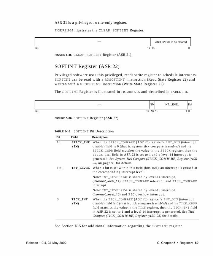
ASR 21 is a privileged, write-only register.
FIGURE 5-35 illustrates the CLEAR_SOFTINT Register.
FIGURE 5-35 CLEAR_SOFTINT Register (ASR 21)
SOFTINT Register (ASR 22)
Privileged software uses this privileged, read/write register to schedule interrupts. SOFTINT can be read with a RDSOFTINT instruction (Read State Register 22) and written with a WRSOFTINT instruction (Write State Register 22).
The SOFTINT Register is illustrated in FIGURE 5-36 and described in TABLE 5-16.
FIGURE 5-36 SOFTINT Register (ASR 22)
See Section N.5 for additional information regarding the SOFTINT register.
TABLE 5-16 SOFTINT Bit Description
Bit Field Description
16 STICK_INT (SM)
When the STICK_COMPARE (ASR 25) register’s INT_DIS (interrupt disable) field is 0 (that is, system tick compare is enabled) and its STICK_CMPR field matches the value in the STICK register, then the STICK_INT field in ASR 22 is set to 1 and a level 14 interrupt is generated. See System Tick Compare (STICK_COMPARE) Register (ASR 25) on page 91 for details.
15:1 INT_LEVEL When a bit is set within this field (bits 15:1), an interrupt is caused at the corresponding interrupt level. Note: INT_LEVEL<14> is shared by level-14 interrupt, (interrupt_level_14), STICK_COMPARE interrupt, and TICK_COMPARE interrupt. Note: INT_LEVEL<15> is shared by level-15 interrupt (interrupt_level_15) and PIC overflow interrupt.
0 TICK_INT (TM)
When the TICK_COMPARE (ASR 23) register’s INT_DIS (interrupt disable) field is 0 (that is, tick compare is enabled) and its TICK_CMPR field matches the value in the TICK register, then the TICK_INT field in ASR 22 is set to 1 and a level-14 interrupt is generated. See Tick Compare (TICK_COMPARE) Register (ASR 23) for details.
0
—
63 17 16
ASR 22 Bits to be cleared
0
—
63 11516
INT_LEVEL
17
SM TM
Release 1.0.4, 31 May 2002 C. Chapter 5 • Registers 89

Tick Compare (TICK_COMPARE) Register (ASR 23)
The TICK register is used for fine-grained measurements of time in processor cycles. The TICK_COMPARE register allows system software to cause a trap when the TICK register reaches a specified value. Nonprivileged accesses to this register cause a privileged_opcode trap (see Exception and Interrupt Descriptions on page 161). After a power-on reset trap, the INT_DIS bit is set to 1 (disabling tick compare interrupts) and the TICK_CMPR value is set to 0.
The TICK_COMPARE Register is described below and illustrated in FIGURE 5-37.
FIGURE 5-37 TICK_COMPARE Register
System Tick (STICK) Register (ASR 24)
The counter field of the STICK register is a 63-bit counter that increments at a rate determined by a clock signal external to the processor. Bit 63 of the STICK register is the nonprivileged trap (NPT) bit, which controls access to the STICK register by nonprivileged software. Privileged software can always read the STICK register with RDSTICK instruction. Privileged software can always write the STICK register with the WRSTICK instruction.
The STICK register is illustrated in FIGURE 5-38 and described below.
FIGURE 5-38 STICK Register
Nonprivileged software can read the STICK register by using the RDSTICK instruction when STICK.NPT = 0. When STICK.NPT = 1, an attempt by nonprivileged software to read the STICK register causes a privileged_action
Bit Field Description
63 INT_DIS Interrupt Disable. If set, tick compare interrupts are disabled.62:0 TICK_CMPR Tick Compare Field. When this field exactly matches TICK.counter and
TICK_COMPARE.INT_DIS = 0, a TICK_INT is posted in the SOFTINT register. This has the effect of posting a level-14 interrupt to the processor when the processor has (PIL < 14) and (PSTATE.IE = 1). The level-14 interrupt handler must check SOFTINT<14>, TICK_INT, and STICK_INT to determine which was the source of the level-14 interrupt.
063 62
TICK_COMPARE INT_DIS TICK_CMPR
063 62
STICK NPT counter
90 SPARC® Joint Programming Specification (JPS1): Commonality • Release 1.0.4, 31 May 2002
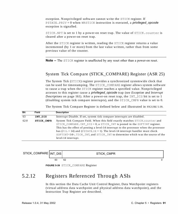
exception. Nonprivileged software cannot write the STICK register. If PSTATE.PRIV = 0 when WRSTICK instruction is executed, a privileged_opcode exception is signalled.
STICK.NPT is set to 1 by a power-on reset trap. The value of STICK.counter is cleared after a power-on reset trap.
After the STICK register is written, reading the STICK register returns a value incremented (by 1 or more) from the last value written, rather than from some previous value of the counter.
Note – The STICK register is unaffected by any reset other than a power-on reset.
System Tick Compare (STICK_COMPARE) Register (ASR 25)
The System Tick (STICK) register provides a synchronized systemwide clock that can be used for timestamping. The STICK_COMPARE register allows system software to cause a trap when the STICK register reaches a specified value. Nonprivileged accesses to this register cause a privileged_opcode trap (see Exception and Interrupt Descriptions on page 161). After a power-on reset trap, the INT_DIS bit is set to 1 (disabling system tick compare interrupts), and the STICK_CMPR value is set to 0.
The System Tick Compare Register is defined below and illustrated in FIGURE 5-39.
FIGURE 5-39 STICK_COMPARE Register
5.2.12 Registers Referenced Through ASIsIn this section the Data Cache Unit Control Register, Data Watchpoint registers (virtual address data watchpoint and physical address data watchpoint), and the Instruction Trap Register are described.
Bit Field Description
63 INT_DIS Interrupt Disable. If set, system tick compare interrupts are disabled.62:0 STICK_CMPR System Tick Compare Field. When this field exactly matches STICK.counter and
STICK_COMPARE.INT_DIS = 0, a STICK_INT is posted in the SOFTINT register. This has the effect of posting a level-14 interrupt to the processor when the processor has (PIL < 14) and (PSTATE.IE = 1). The level-14 interrupt handler must check SOFTINT<14>, TICK_INT, and STICK_INT to determine which was the source of the level-14 interrupt.
063 62
STICK_COMPARE INT_DIS STICK_CMPR
Release 1.0.4, 31 May 2002 C. Chapter 5 • Registers 91
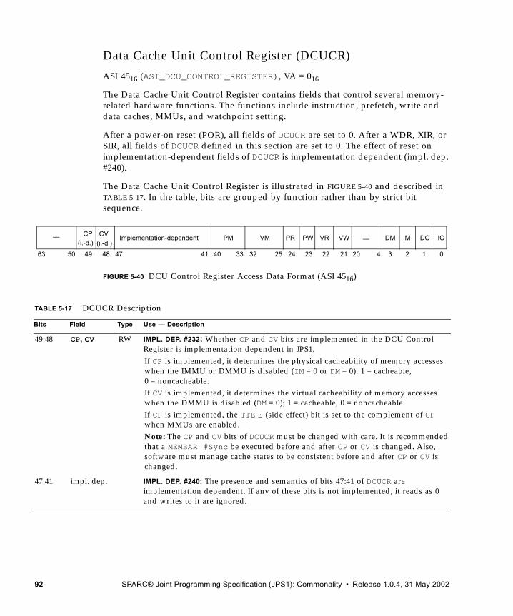
Data Cache Unit Control Register (DCUCR)
ASI 4516 (ASI_DCU_CONTROL_REGISTER), VA = 016
The Data Cache Unit Control Register contains fields that control several memory-related hardware functions. The functions include instruction, prefetch, write and data caches, MMUs, and watchpoint setting.
After a power-on reset (POR), all fields of DCUCR are set to 0. After a WDR, XIR, or SIR, all fields of DCUCR defined in this section are set to 0. The effect of reset on implementation-dependent fields of DCUCR is implementation dependent (impl. dep. #240).
The Data Cache Unit Control Register is illustrated in FIGURE 5-40 and described in TABLE 5-17. In the table, bits are grouped by function rather than by strict bit sequence.
FIGURE 5-40 DCU Control Register Access Data Format (ASI 4516)
TABLE 5-17 DCUCR Description
Bits Field Type Use — Description
49:48 CP, CV RW IMPL. DEP. #232: Whether CP and CV bits are implemented in the DCU Control Register is implementation dependent in JPS1. If CP is implemented, it determines the physical cacheability of memory accesses when the IMMU or DMMU is disabled (IM = 0 or DM = 0). 1 = cacheable, 0 = noncacheable.If CV is implemented, it determines the virtual cacheability of memory accesses when the DMMU is disabled (DM = 0); 1 = cacheable, 0 = noncacheable.If CP is implemented, the TTE E (side effect) bit is set to the complement of CP when MMUs are enabled.Note: The CP and CV bits of DCUCR must be changed with care. It is recommended that a MEMBAR #Sync be executed before and after CP or CV is changed. Also, software must manage cache states to be consistent before and after CP or CV is changed.
47:41 impl. dep. IMPL. DEP. #240: The presence and semantics of bits 47:41 of DCUCR are implementation dependent. If any of these bits is not implemented, it reads as 0 and writes to it are ignored.
Implementation-dependent PM VM PR PW VR DM DC
012342122234041 20
VW
2425323347
IM ICCP
4849
CV
5063
—(i.-d.) (i.-d.)
—
92 SPARC® Joint Programming Specification (JPS1): Commonality • Release 1.0.4, 31 May 2002
Watchpoint Control
40:33 PM<7:0> DCU Physical Address Data Watchpoint Mask. The Physical Address Data Watchpoint Register contains the physical address of a 64-bit word to be watched. The 8-bit Physical Address Data Watch Point Mask controls which byte(s) within the 64-bit word should be watched. If all 8 bits are cleared, the physical watchpoint is disabled. If the watchpoint is enabled and a data reference overlaps any of the watched bytes in the watchpoint mask, then a physical watchpoint trap is generated. Watchpoint behavior for a Partial Store instruction may differ (see impl. dep. #249).Please see the table in the VM field description.
32:25 VM<7:0> DCU Virtual Address Data Watchpoint Mask. The Virtual Address Data Watchpoint Register contains the virtual address of a 64-bit word to be watched. This 8-bit mask controls which byte(s) within the 64-bit word should be watched. If all 8 bits are cleared, then the virtual watchpoint is disabled. If watchpoint is enabled and a data reference overlaps any of the watched bytes in the watchpoint mask, then a virtual watchpoint trap is generated. Watchpoint behavior for a Partial Store instruction may differ (see impl. dep. #249).VA/PA data watchpoint byte mask examples are shown below.
24, 23 PR, PW DCU Physical Address Data Watchpoint Enable. If PR (PW) is 1, then a data read (write) that matches the range of addresses in the Physical Watchpoint Register causes a watchpoint trap. If both PR and PW are set, a watchpoint trap will occur on either a read or write access.
22, 21 VR, VW DCU Virtual Address Data Watchpoint Enable. If VR (VW) is 1, then a data read (write) that matches the range of addresses in the Virtual Watchpoint Register causes a watchpoint trap. If both VR and VW are set, a watchpoint trap will occur on either a read or write access.
20:4 — Reserved.
MMU Control
3 DM DMMU Enable. If DM = 0, the DMMU is disabled (pass-through mode).Note: When the MMU/TLB is disabled, a virtual address is passed through as a physical address.
2 IM IMMU Enable. If IM = 0, the IMMU is disabled (pass-through mode).
TABLE 5-17 DCUCR Description (Continued)
Bits Field Type Use — Description
Watchpoint Mask(PM or VM)
Least Significant 3 Bits ofAddress of Bytes Watched7654 3210
0016 Watchpoint disabled0116 0000 00013216 0011 0010FF16 1111 1111
Release 1.0.4, 31 May 2002 C. Chapter 5 • Registers 93
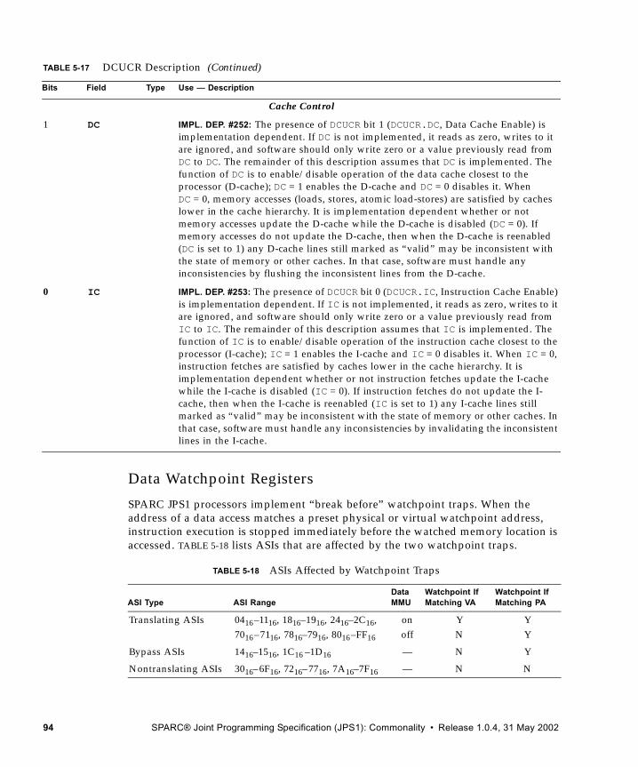
Data Watchpoint Registers
SPARC JPS1 processors implement “break before” watchpoint traps. When the address of a data access matches a preset physical or virtual watchpoint address, instruction execution is stopped immediately before the watched memory location is accessed. TABLE 5-18 lists ASIs that are affected by the two watchpoint traps.
Cache Control
1 DC IMPL. DEP. #252: The presence of DCUCR bit 1 (DCUCR.DC, Data Cache Enable) is implementation dependent. If DC is not implemented, it reads as zero, writes to it are ignored, and software should only write zero or a value previously read from DC to DC. The remainder of this description assumes that DC is implemented. The function of DC is to enable/disable operation of the data cache closest to the processor (D-cache); DC = 1 enables the D-cache and DC = 0 disables it. When DC = 0, memory accesses (loads, stores, atomic load-stores) are satisfied by caches lower in the cache hierarchy. It is implementation dependent whether or not memory accesses update the D-cache while the D-cache is disabled (DC = 0). If memory accesses do not update the D-cache, then when the D-cache is reenabled (DC is set to 1) any D-cache lines still marked as “valid” may be inconsistent with the state of memory or other caches. In that case, software must handle any inconsistencies by flushing the inconsistent lines from the D-cache.
0 IC IMPL. DEP. #253: The presence of DCUCR bit 0 (DCUCR.IC, Instruction Cache Enable) is implementation dependent. If IC is not implemented, it reads as zero, writes to it are ignored, and software should only write zero or a value previously read from IC to IC. The remainder of this description assumes that IC is implemented. The function of IC is to enable/disable operation of the instruction cache closest to the processor (I-cache); IC = 1 enables the I-cache and IC = 0 disables it. When IC = 0, instruction fetches are satisfied by caches lower in the cache hierarchy. It is implementation dependent whether or not instruction fetches update the I-cache while the I-cache is disabled (IC = 0). If instruction fetches do not update the I-cache, then when the I-cache is reenabled (IC is set to 1) any I-cache lines still marked as “valid” may be inconsistent with the state of memory or other caches. In that case, software must handle any inconsistencies by invalidating the inconsistent lines in the I-cache.
TABLE 5-18 ASIs Affected by Watchpoint Traps
ASI Type ASI RangeData MMU
Watchpoint If Matching VA
Watchpoint If Matching PA
Translating ASIs 0416–1116, 1816–1916, 2416–2C16,7016–7116, 7816–7916, 8016–FF16
onoff
YN
YY
Bypass ASIs 1416–1516, 1C16 –1D16 — N Y
Nontranslating ASIs 3016–6F16, 7216–7716, 7A16–7F16 — N N
TABLE 5-17 DCUCR Description (Continued)
Bits Field Type Use — Description
94 SPARC® Joint Programming Specification (JPS1): Commonality • Release 1.0.4, 31 May 2002
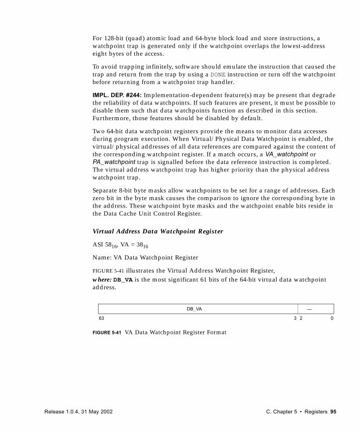
For 128-bit (quad) atomic load and 64-byte block load and store instructions, a watchpoint trap is generated only if the watchpoint overlaps the lowest-address eight bytes of the access.
To avoid trapping infinitely, software should emulate the instruction that caused the trap and return from the trap by using a DONE instruction or turn off the watchpoint before returning from a watchpoint trap handler.
IMPL. DEP. #244: Implementation-dependent feature(s) may be present that degrade the reliability of data watchpoints. If such features are present, it must be possible to disable them such that data watchpoints function as described in this section. Furthermore, those features should be disabled by default.
Two 64-bit data watchpoint registers provide the means to monitor data accesses during program execution. When Virtual/Physical Data Watchpoint is enabled, the virtual/physical addresses of all data references are compared against the content of the corresponding watchpoint register. If a match occurs, a VA_watchpoint or PA_watchpoint trap is signalled before the data reference instruction is completed. The virtual address watchpoint trap has higher priority than the physical address watchpoint trap.
Separate 8-bit byte masks allow watchpoints to be set for a range of addresses. Each zero bit in the byte mask causes the comparison to ignore the corresponding byte in the address. These watchpoint byte masks and the watchpoint enable bits reside in the Data Cache Unit Control Register.
Virtual Address Data Watchpoint Register
ASI 5816, VA = 3816
Name: VA Data Watchpoint Register
FIGURE 5-41 illustrates the Virtual Address Watchpoint Register, where: DB_VA is the most significant 61 bits of the 64-bit virtual data watchpoint address.
FIGURE 5-41 VA Data Watchpoint Register Format
63 23 0
—DB_VA
Release 1.0.4, 31 May 2002 C. Chapter 5 • Registers 95
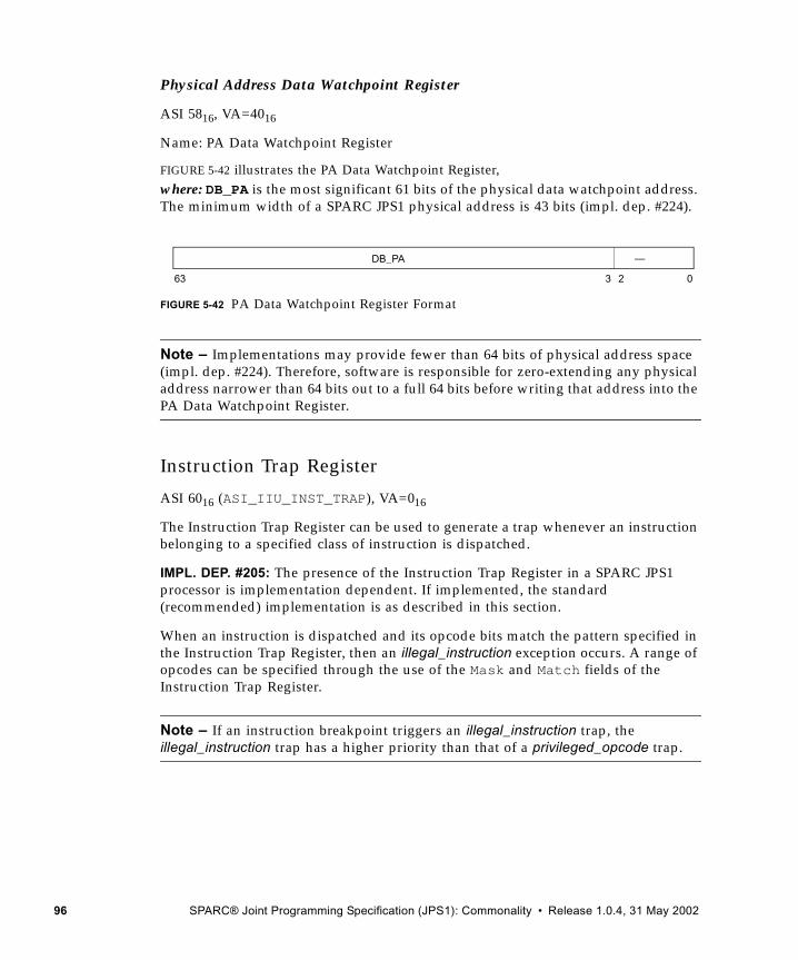
Physical Address Data Watchpoint Register
ASI 5816, VA=4016
Name: PA Data Watchpoint Register
FIGURE 5-42 illustrates the PA Data Watchpoint Register, where: DB_PA is the most significant 61 bits of the physical data watchpoint address. The minimum width of a SPARC JPS1 physical address is 43 bits (impl. dep. #224).
FIGURE 5-42 PA Data Watchpoint Register Format
Note – Implementations may provide fewer than 64 bits of physical address space (impl. dep. #224). Therefore, software is responsible for zero-extending any physical address narrower than 64 bits out to a full 64 bits before writing that address into the PA Data Watchpoint Register.
Instruction Trap Register
ASI 6016 (ASI_IIU_INST_TRAP), VA=016
The Instruction Trap Register can be used to generate a trap whenever an instruction belonging to a specified class of instruction is dispatched.
IMPL. DEP. #205: The presence of the Instruction Trap Register in a SPARC JPS1 processor is implementation dependent. If implemented, the standard (recommended) implementation is as described in this section.
When an instruction is dispatched and its opcode bits match the pattern specified in the Instruction Trap Register, then an illegal_instruction exception occurs. A range of opcodes can be specified through the use of the Mask and Match fields of the Instruction Trap Register.
Note – If an instruction breakpoint triggers an illegal_instruction trap, the illegal_instruction trap has a higher priority than that of a privileged_opcode trap.
63 23 0
—DB_PA
96 SPARC® Joint Programming Specification (JPS1): Commonality • Release 1.0.4, 31 May 2002
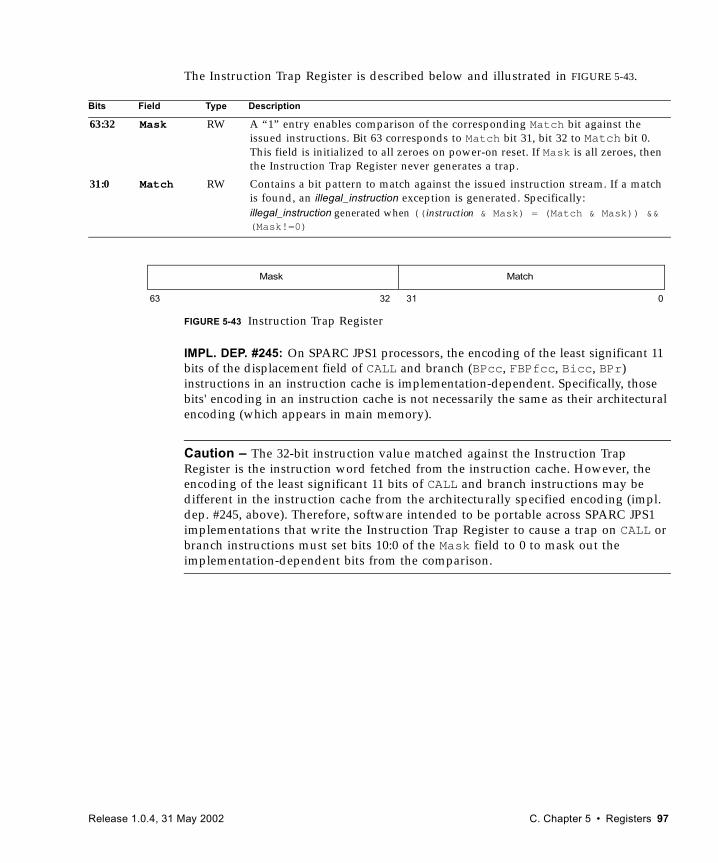
The Instruction Trap Register is described below and illustrated in FIGURE 5-43.
FIGURE 5-43 Instruction Trap Register
IMPL. DEP. #245: On SPARC JPS1 processors, the encoding of the least significant 11 bits of the displacement field of CALL and branch (BPcc, FBPfcc, Bicc, BPr) instructions in an instruction cache is implementation-dependent. Specifically, those bits' encoding in an instruction cache is not necessarily the same as their architectural encoding (which appears in main memory).
Caution – The 32-bit instruction value matched against the Instruction Trap Register is the instruction word fetched from the instruction cache. However, the encoding of the least significant 11 bits of CALL and branch instructions may be different in the instruction cache from the architecturally specified encoding (impl. dep. #245, above). Therefore, software intended to be portable across SPARC JPS1 implementations that write the Instruction Trap Register to cause a trap on CALL or branch instructions must set bits 10:0 of the Mask field to 0 to mask out the implementation-dependent bits from the comparison.
Bits Field Type Description
63:32 Mask RW A “1” entry enables comparison of the corresponding Match bit against the issued instructions. Bit 63 corresponds to Match bit 31, bit 32 to Match bit 0. This field is initialized to all zeroes on power-on reset. If Mask is all zeroes, then the Instruction Trap Register never generates a trap.
31:0 Match RW Contains a bit pattern to match against the issued instruction stream. If a match is found, an illegal_instruction exception is generated. Specifically:illegal_instruction generated when ((instruction & Mask) = (Match & Mask)) && (Mask!=0)
Mask
63 32 31 0
Match
Release 1.0.4, 31 May 2002 C. Chapter 5 • Registers 97
Notes – (1) The Instruction Trap Register generates an exception based on instruction opcodes, not on their addresses (as do traditional breakpoints).
(2) A store to the Instruction Trap Register requires MEMBAR #Sync plus either FLUSH, DONE, or RETRY before the point that its effect must be visible to instruction accesses. That is, MEMBAR #Sync alone is not sufficient. In either case, one of these instructions must be executed before the next noninternal store or load of any type, to avoid data corruption.
As a historical note: This mechanism was designed to provide a way around hardware errors that may be found in silicon during bringup. For example, if an instruction is failing on a particular mask set, it can be trapped and emulated in software with the Instruction Trap Register mechanism.
Interrupt ASI Registers
See Interrupt ASI Registers on page 556 for detailed descriptions of ASI register used in handling interrupts.
5.2.13 Floating-Point Deferred-Trap Queue (FQ)If present in an implementation, the FQ contains sufficient state information to implement resumable, deferred floating-point traps.
IMPL. DEP. #23: Floating-point traps may be precise or deferred. If deferred, a floating-point deferred-trap queue (FQ) shall be present.
The FQ can be read with the read privileged register (RDPR) floating-point queue instruction. In a given implementation, it may also be readable or writable through privileged load/store double alternate instructions (LDDA, STDA) or by read/write ancillary state register instructions (RDASR, WRASR).
IMPL. DEP. #24: The presence, contents of, and operations upon the FQ are implementation dependent.
If an FQ is present, supervisor software must be able to deduce the exception-causing instruction’s opcode, operands, and address from its FQ entry. This also must be true of any other pending floating-point operation in the queue.
In an implementation with a floating-point queue, an attempt to read the FQ with a RDPR instruction when the FQ is empty (FSR.qne = 0) shall cause an fp_exception_other trap with FSR.ftt set to 4 (sequence_error).
In an implementation without an FQ, the qne bit in the FSR is always 0 and an attempt to read FQ with an RDPR instruction causes an illegal_instruction exception.
98 SPARC® Joint Programming Specification (JPS1): Commonality • Release 1.0.4, 31 May 2002
No SPARC JPS1 implementations are expected to make use of deferred traps for floating-point exceptions or to implement a floating-point deferred-trap queue.
5.2.14 Integer Unit Deferred-Trap QueueAn implementation may contain zero or more IU deferred-trap queues. Such a queue contains sufficient state to implement resumable deferred traps caused by the IU. Note: Deferred floating-point traps are handled by the floating-point deferred-trap queue.
IMPL. DEP. #16: The existence, contents, and operation of an IU deferred-trap queue are implementation dependent; it is not visible to user application programs under normal conditions.
No SPARC JPS1 implementations are expected to implement an IU deferred-trap queue.
Release 1.0.4, 31 May 2002 C. Chapter 5 • Registers 99

100 SPARC® Joint Programming Specification (JPS1): Commonality • Release 1.0.4, 31 May 2002
C.CHAPTER 6
Instructions
Instructions are accessed by the processor from memory and are executed, annulled, or trapped. Instructions are encoded in 4 major formats and partitioned into 11 general categories. We describe instructions in these sections:
■ Instruction Execution on page 101■ Instruction Formats and Fields on page 102■ Instruction Categories on page 106■ Register Window Management on page 126
6.1 Instruction ExecutionThe instruction at the memory location specified by the program counter is fetched and then executed. Instruction execution may change program-visible processor and/or memory state. As a side effect of its execution, new values are assigned to the program counter (PC) and the next program counter (nPC).
An instruction may generate an exception if it encounters some condition that makes it impossible to complete normal execution. Such an exception may in turn generate a precise trap. Other events may also cause traps: an exception caused by a previous instruction (a deferred trap), an interrupt or asynchronous error (a disrupting trap), or a reset request (a reset trap). If a trap occurs, control is vectored into a trap table. See Chapter 7, Traps, for a detailed description of exception and trap processing.
If a trap does not occur and the instruction is not a control transfer, the next program counter is copied into the PC, and the nPC is incremented by 4 (ignoring overflow, if any). If the instruction is a control-transfer instruction, the next program counter is copied into the PC and the target address is written to nPC. Thus, the two program counters provide for a delayed-branch execution model.
Release 1.0.4, 31 May 2002 C. Chapter 6 • Instructions 101
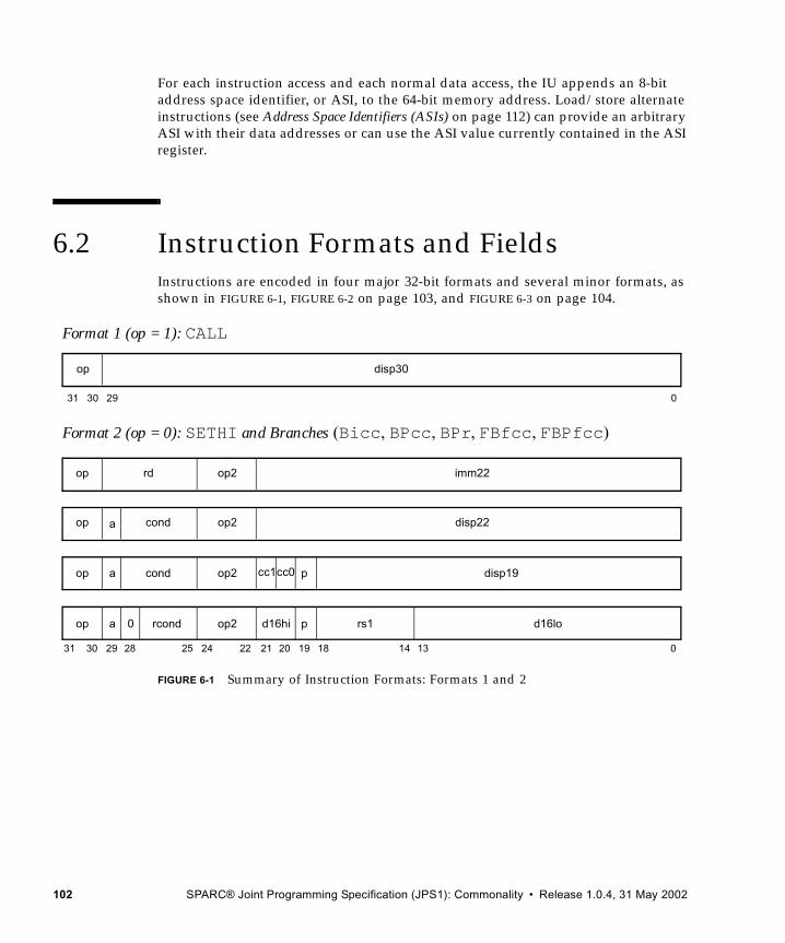
For each instruction access and each normal data access, the IU appends an 8-bit address space identifier, or ASI, to the 64-bit memory address. Load/store alternate instructions (see Address Space Identifiers (ASIs) on page 112) can provide an arbitrary ASI with their data addresses or can use the ASI value currently contained in the ASI register.
6.2 Instruction Formats and FieldsInstructions are encoded in four major 32-bit formats and several minor formats, as shown in FIGURE 6-1, FIGURE 6-2 on page 103, and FIGURE 6-3 on page 104.
FIGURE 6-1 Summary of Instruction Formats: Formats 1 and 2
31 030 29
disp30op
Format 1 (op = 1): CALL
Format 2 (op = 0): SETHI and Branches (Bicc, BPcc, BPr, FBfcc, FBPfcc)
31 2224 21 02530 29
disp22op2condop a
disp19op2condop a
d16loop2rcondop a
20 19 1828
0
cc1cc0 p
pd16hi
14 13
rs1
imm22op2rdop
102 SPARC® Joint Programming Specification (JPS1): Commonality • Release 1.0.4, 31 May 2002
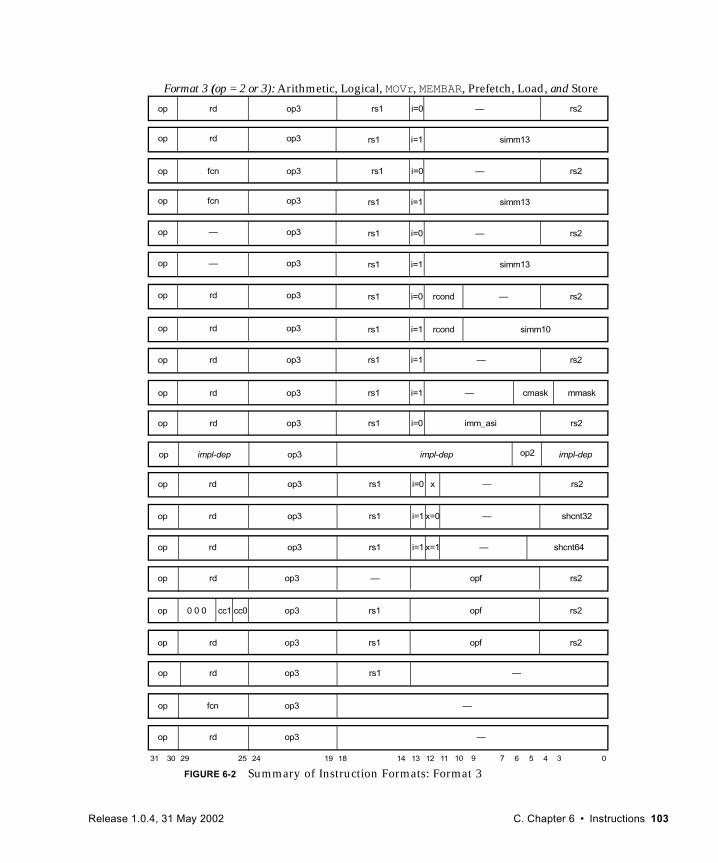
FIGURE 6-2 Summary of Instruction Formats: Format 3
op3rdop rs1 i=1 mmask
Format 3 (op = 2 or 3): Arithmetic, Logical, MOVr, MEMBAR, Prefetch, Load, and Store
op3rdop —rs1 i=0 rs2
op3rdop rs1 i=1 simm13
op3rdop rcondrs1 i=0 rs2
op3rdop rs1 i=1 simm10rcond
—
—
op3rdop rs1 i=1 rs2—
op3—op —rs1 i=0 rs2
op3—op rs1 i=1 simm13
cmask
op rd op3 rs1 i=0 imm_asi rs2
op3impl-depop impl-dep
31 24 02530 29 19 18
rdop op3 —
14 13 12 5 4
rs1 rs2i=0 x
rdop op3 —rs1 shcnt32i=1 x=0
rdop op3 —rs1 shcnt64i=1 x=1
6
op fcn op3 —
11
op3rdop rs1 —
op3rdop —
op3rdop rs2opf—
op3rdop rs1 rs2opf
op op3 rs20 0 0 rs1 opfcc1 cc0
10 9 8 7 3
op3fcnop —rs1 i=0 rs2
op3fcnop rs1 i=1 simm13
op2 impl-dep
Release 1.0.4, 31 May 2002 C. Chapter 6 • Instructions 103
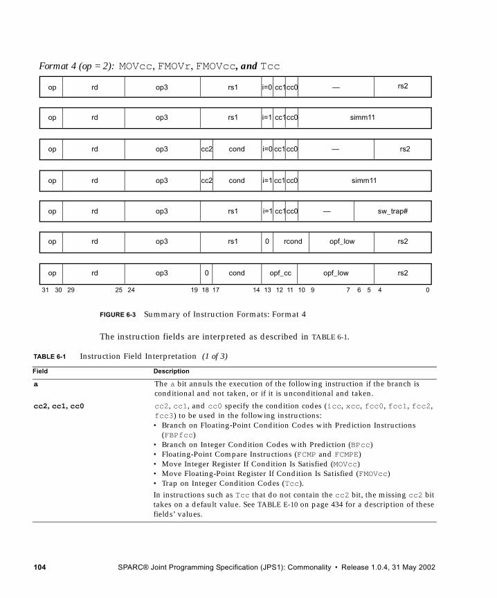
FIGURE 6-3 Summary of Instruction Formats: Format 4
The instruction fields are interpreted as described in TABLE 6-1.
TABLE 6-1 Instruction Field Interpretation (1 of 3)
Field Description
a The a bit annuls the execution of the following instruction if the branch is conditional and not taken, or if it is unconditional and taken.
cc2, cc1, cc0 cc2, cc1, and cc0 specify the condition codes (icc, xcc, fcc0, fcc1, fcc2, fcc3) to be used in the following instructions: • Branch on Floating-Point Condition Codes with Prediction Instructions
(FBPfcc)• Branch on Integer Condition Codes with Prediction (BPcc)• Floating-Point Compare Instructions (FCMP and FCMPE)• Move Integer Register If Condition Is Satisfied (MOVcc)• Move Floating-Point Register If Condition Is Satisfied (FMOVcc)• Trap on Integer Condition Codes (Tcc). In instructions such as Tcc that do not contain the cc2 bit, the missing cc2 bit takes on a default value. See TABLE E-10 on page 434 for a description of these fields’ values.
op3rdop rs1 i=0 rs2
op3rdop rs1 i=1 sw_trap#
cc1cc0 —
cc1cc0
Format 4 (op = 2): MOVcc, FMOVr, FMOVcc, and Tcc
op3rdop rs1 i=1 simm11
31 141924 18 13 12 5 4 02530 29 11 10 9
cc1cc0
7 6
—
op rd op3 cond opf_cc opf_low rs2
op rd op3 0 rcond opf_low rs2rs1
0
17
rdop op3 —cond rs2i=0
rdop op3 cond simm11i=1
cc2
cc2
cc1
cc1
cc0
cc0
104 SPARC® Joint Programming Specification (JPS1): Commonality • Release 1.0.4, 31 May 2002
cmask This 3-bit field specifies sequencing constraints on the order of memory references and the processing of instructions before and after a MEMBAR instruction.
cond This 4-bit field selects the condition tested by a branch instruction. See Appendix E, Opcode Maps, for descriptions of its values.
d16hi, d16lo These 2-bit and 14-bit fields together comprise a word-aligned, sign-extended, PC-relative displacement for a branch-on-register-contents with prediction (BPr) instruction.
disp19 This 19-bit field is a word-aligned, sign-extended, PC-relative displacement for an integer branch-with-prediction (BPcc) instruction or a floating-point branch-with-prediction (FBPfcc) instruction.
disp22, disp30 These 22-bit and 30-bit fields are word-aligned, sign-extended, PC-relative displacements for a branch or call, respectively.
fcn This 5-bit field provides additional opcode bits to encode the DONE, RETRY, and PREFETCH(A) instructions.
i The i bit selects the second operand for integer arithmetic and load/store instructions. If i = 0, then the operand is r[rs2]. If i = 1, then the operand is simm10, simm11, or simm13, depending on the instruction, sign-extended to 64 bits.
imm22 This 22-bit field is a constant that SETHI places in bits 31:10 of a destination register.
imm_asi This 8-bit field is the address space identifier in instructions that access alternate space.
impl-dep The meaning of these fields is completely implementation dependent for IMPDEP2A and IMPDEP2B instructions.
mmask This 4-bit field imposes order constraints on memory references appearing before and after a MEMBAR instruction.
op, op2 These 2- and 3-bit fields encode the three major formats and the Format 2 instructions. See Appendix E, Opcode Maps, for descriptions of their values.
op3 This 6-bit field (together with one bit from op) encodes the Format 3 instructions. See Appendix E, Opcode Maps, for descriptions of its values.
opf This 9-bit field encodes the operation for a floating-point operate (FPop) instruction. See Appendix E, Opcode Maps, for possible values and their meanings.
opf_cc Specifies the condition codes to be used in FMOVcc instructions. See cc0, cc1, and cc2 above for details.
opf_low This 6-bit field encodes the specific operation for a Move Floating-Point Register if condition is satisfied (FMOVcc) or Move Floating-Point Register if contents of integer register match condition (FMOVr) instruction.
TABLE 6-1 Instruction Field Interpretation (2 of 3)
Field Description
Release 1.0.4, 31 May 2002 C. Chapter 6 • Instructions 105
6.3 Instruction CategoriesSPARC V9 instructions can be grouped into the following categories:
■ Memory access■ Memory synchronization■ Integer arithmetic■ Control transfer (CTI)■ Conditional moves■ Register window management■ State register access
p This 1-bit field encodes static prediction for BPcc and FBPfcc instructions; branch prediction bit (p) encodings are shown below.
rcond This 3-bit field selects the register-contents condition to test for a move, based on register contents (MOVr or FMOVr) instruction or a Branch on Register Contents with Prediction (BPr) instruction. See Appendix E, Opcode Maps, for descriptions of its values.
rd This 5-bit field is the address of the destination (or source) r or f register(s) for a load, arithmetic, or store instruction.
rs1 This 5-bit field is the address of the first r or f register(s) source operand.
rs2 This 5-bit field is the address of the second r or f register(s) source operand with i = 0.
shcnt32 This 5-bit field provides the shift count for 32-bit shift instructions.
shcnt64 This 6-bit field provides the shift count for 64-bit shift instructions.
simm10 This 10-bit field is an immediate value that is sign-extended to 64 bits and used as the second ALU operand for a MOVr instruction when i = 1.
simm11 This 11-bit field is an immediate value that is sign-extended to 64 bits and used as the second ALU operand for a MOVcc instruction when i = 1.
simm13 This 13-bit field is an immediate value that is sign-extended to 64 bits and used as the second ALU operand for an integer arithmetic instruction or for a load/store instruction when i = 1.
sw_trap# This 7-bit field is an immediate value that is used as the second ALU operand for a Trap on Condition Code instruction.
x The x bit selects whether a 32- or 64-bit shift will be performed.
TABLE 6-1 Instruction Field Interpretation (3 of 3)
Field Description
p Branch Prediction
0 Predict that branch will not be taken
1 Predict that branch will be taken
106 SPARC® Joint Programming Specification (JPS1): Commonality • Release 1.0.4, 31 May 2002
■ Privileged register access■ Floating-point operate■ Implementation dependent■ Reserved
Each of these categories is described in the following subsections.
6.3.1 Memory Access InstructionsLoad, store, load-store, and PREFETCH instructions are the only instructions that access memory. All of the instructions except Compare and Swap use either two r registers or an r register and simm13 to calculate a 64-bit byte memory address. Compare and Swap uses a single r register to specify a 64-bit byte memory address. To this 64-bit address, the IU appends an ASI that encodes address space information.
The destination field of a memory reference instruction specifies the r or f register(s) that supply the data for a store or that receive the data from a load or LDSTUB. For SWAP, the destination register identifies the r register to be exchanged atomically with the calculated memory location. For Compare and Swap, an r register is specified, the value of which is compared with the value in memory at the computed address. If the values are equal, then the destination field specifies the r register that is to be exchanged atomically with the addressed memory location. If the values are unequal, then the destination field specifies the r register that is to receive the value at the addressed memory location; in this case, the addressed memory location remains unchanged.
The destination field of a PREFETCH instruction (fcn) is used to encode the type of the prefetch.
Integer load and store instructions support byte (8-bit), halfword (16-bit), word (32-bit), and doubleword (64-bit) accesses. Floating-point load and store instructions support word, doubleword, and quadword memory accesses. LDSTUB accesses bytes, SWAP accesses words, CASA accesses words, and CASXA accesses doublewords. The Atomic Quad Load instruction accesses a quadword (16 bytes) Block load and store access eight consecutive doublewords. PREFETCH accesses at least 64 bytes.
Release 1.0.4, 31 May 2002 C. Chapter 6 • Instructions 107
Programming Note – By setting i = 1 and rs1 = 0, you can access any location in the lowest or highest 4 Kbytes of an address space without using a register to hold part of the address.
Memory Alignment Restrictions
Halfword accesses must be aligned on 2-byte boundaries, word accesses (which include instruction fetches) must be aligned on 4-byte boundaries, extended word and doubleword accesses must be aligned on 8-byte boundaries, quadword accesses must be aligned on 16-byte boundaries, and Block load and Block store accesses must be aligned on 64-byte boundaries.
Double-precision floating-point values may be aligned on word boundaries. However, if so aligned, doubleword loads/stores may not be used to access them, resulting in less efficient and nonatomic accesses.
An improperly aligned address in a load, store, or load-store instruction causes a mem_address_not_aligned exception to occur, with these exceptions:
■ An LDDF or LDDFA instruction accessing an address that is word aligned but not doubleword aligned causes an LDDF_mem_address_not_aligned exception.
■ An STDF or STDFA instruction accessing an address that is word aligned but not doubleword aligned causes an STDF_mem_address_not_aligned exception.
Addressing Conventions
The processor uses big-endian byte order for all instruction accesses and, by default, for data accesses. It is possible to access data in little-endian format by using selected ASIs. It is also possible to change the default byte order for implicit data accesses. See Processor State (PSTATE) Register on page 69 for more information.1
1. See also Cohen, D., “On Holy Wars and a Plea for Peace,” Computer 14:10 (October 1981), pp. 48-54.
108 SPARC® Joint Programming Specification (JPS1): Commonality • Release 1.0.4, 31 May 2002
Big-endian Addressing Convention. Within a multiple-byte integer, the byte with the smallest address is the most significant; a byte’s significance decreases as its address increases. The big-endian addressing conventions are illustrated in FIGURE 6-4 and described below the figure.
FIGURE 6-4 Big-endian Addressing Conventions
byte A load/store byte instruction accesses the addressed byte in both big- and little-endian modes.
halfword For a load/store halfword instruction, two bytes are accessed. The most significant byte (bits 15–8) is accessed at the address specified in the instruction; the least significant byte (bits 7–0) is accessed at the address + 1.
Byte7 0
Halfword15 0
Word31 0
Doubleword /63 32
31 0
78
15 78162324
47 3940485556
15 78162324
0 1
00 01 10 11
Address
Address<0> =
Address<1:0> =
Address<2:0> =
Address<2:0> =
000 001 010 011
100 101 110 111
Quadword127 96
95 64
111 103104112119120
79 7172808788
Address<3:0> =
Address<3:0> =
0000 0001 0010 0011
0100 0101 0110 0111
63 32
31 0
47 3940485556
15 78162324
Address<3:0> =
Address<3:0> =
1000 1001 1010 1011
1100 1101 1110 1111
Extended word
Release 1.0.4, 31 May 2002 C. Chapter 6 • Instructions 109
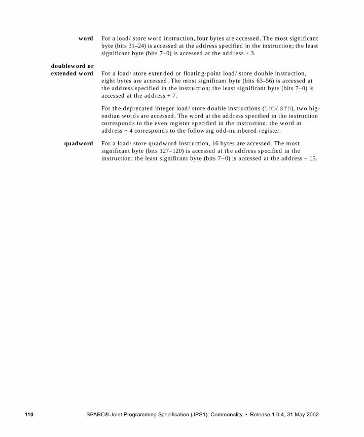
word For a load/store word instruction, four bytes are accessed. The most significant byte (bits 31–24) is accessed at the address specified in the instruction; the least significant byte (bits 7–0) is accessed at the address + 3.
doubleword orextended word For a load/store extended or floating-point load/store double instruction,
eight bytes are accessed. The most significant byte (bits 63–56) is accessed at the address specified in the instruction; the least significant byte (bits 7–0) is accessed at the address + 7.
For the deprecated integer load/store double instructions (LDD/STD), two big-endian words are accessed. The word at the address specified in the instruction corresponds to the even register specified in the instruction; the word at address + 4 corresponds to the following odd-numbered register.
quadword For a load/store quadword instruction, 16 bytes are accessed. The most significant byte (bits 127–120) is accessed at the address specified in the instruction; the least significant byte (bits 7–0) is accessed at the address + 15.
110 SPARC® Joint Programming Specification (JPS1): Commonality • Release 1.0.4, 31 May 2002
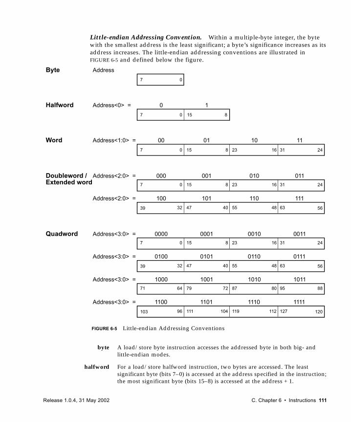
Little-endian Addressing Convention. Within a multiple-byte integer, the byte with the smallest address is the least significant; a byte’s significance increases as its address increases. The little-endian addressing conventions are illustrated in FIGURE 6-5 and defined below the figure.
byte A load/store byte instruction accesses the addressed byte in both big- and little-endian modes.
halfword For a load/store halfword instruction, two bytes are accessed. The least significant byte (bits 7–0) is accessed at the address specified in the instruction; the most significant byte (bits 15–8) is accessed at the address + 1.
Byte7 0
Halfword7 8
Word7 24
Doubleword /
150
23 31168150
0 1
00 01 10 11
Address
Address<0> =
Address<1:0> =
Address<2:0> =
Address<2:0> =
000 001 010 011
100 101 110 111
Quadword Address<3:0> =
Address<3:0> =
0000 0001 0010 0011
0100 0101 0110 0111
Address<3:0> =
Address<3:0> =
1000 1001 1010 1011
1100 1101 1110 1111
39 5655 6348404732
7 2423 31168150
39 5655 6348404732
7 2423 31168150
103 120119 12711210411196
71 8887 9580727964
Extended word
FIGURE 6-5 Little-endian Addressing Conventions
Release 1.0.4, 31 May 2002 C. Chapter 6 • Instructions 111
word For a load/store word instruction, four bytes are accessed. The least significant byte (bits 7–0) is accessed at the address specified in the instruction; the most significant byte (bits 31–24) is accessed at the address + 3.
doubleword orextended word For a load/store extended or floating-point load/store double instruction,
eight bytes are accessed. The least significant byte (bits 7–0) is accessed at the address specified in the instruction; the most significant byte (bits 63–56) is accessed at the address + 7.
For the deprecated integer load/store double instructions (LDD/STD), two little-endian words are accessed. The word at the address specified in the instruction corresponds to the even register in the instruction; the word at the address specified in the instruction +4 corresponds to the following odd-numbered register. With respect to little endian memory, an LDD (STD} instruction behaves as if it is composed of two 32-bit loads (stores), each of which is byte-swapped independently before being written into each destination register (memory word).
quadword For a load/store quadword instruction, 16 bytes are accessed. The least significant byte (bits 7–0) is accessed at the address specified in the instruction; the most significant byte (bits 127–120) is accessed at the address + 15.
Address Space Identifiers (ASIs)
Load and store instructions provide an implicit ASI value of ASI_PRIMARY, ASI_PRIMARY_LITTLE, ASI_NUCLEUS, or ASI_NUCLEUS_LITTLE (see Addressing and Alternate Address Spaces on page 173). Load and store alternate instructions provide an explicit ASI, specified by the imm_asi instruction field when i = 0, or the contents of the ASI register when i = 1.
ASIs 0016 through 7F16 are restricted; only privileged software is allowed to access them. An attempt to access a restricted ASI by nonprivileged software results in a privileged_action exception. ASIs 8016 through FF16 are unrestricted; software is allowed to access them whether the processor is operating in privileged or nonprivileged mode, as summarized in TABLE 6-2.
TABLE 6-2 Allowed Accesses to ASIs
Value Access TypeProcessor State(PSTATE.PRIV) Result of ASI Access
0016–7F16 Restricted Nonprivileged (0) privileged_action exception
Privileged (1) Valid access
8016–FF16 Unrestricted Nonprivileged (0) Valid access
Privileged (1) Valid access
112 SPARC® Joint Programming Specification (JPS1): Commonality • Release 1.0.4, 31 May 2002
IMPL. DEP. #29: In SPARC V9, many ASIs were defined to be implementation dependent. Some of those ASIs have been allocated for standard uses in SPARC JPS1. Others remain implementation dependent in SPARC JPS1. See TABLE L-1 on page 539 for details.
IMPL. DEP. #30: In SPARC V9, an implementation could choose to decode only a subset of the 8-bit ASI specifier. In SPARC JPS1 implementations, all 8 bits of each ASI specifier must be decoded. Refer to Appendix L, Address Space Identifiers, of this specification for details.
Separate Instruction Memory
A SPARC V9 implementation may choose to access instruction and data through the same address space and use hardware to keep data and instruction memory consistent at all times. It may also choose to overload independent address spaces for data and instructions and allow them to become inconsistent when data writes are made to addresses shared with the instruction space.
A SPARC V9 program containing self-modifying code should use FLUSH instruction(s) after executing stores to modify instruction memory and before executing the modified instruction(s), to ensure the consistency of program execution.
Memory Synchronization Instructions
Two forms of memory barrier (MEMBAR) instructions allow programs to manage the order and completion of memory references. Ordering MEMBARs induce a partial ordering between sets of loads and stores and future loads and stores. Sequencing MEMBARs exert explicit control over completion of loads and stores (or other instructions). Both barrier forms are encoded in a single instruction, with subfunctions bit-encoded in an immediate field.
6.3.2 Integer Arithmetic InstructionsThe integer arithmetic instructions are generally triadic-register-address instructions that compute a result that is a function of two source operands. They either write the result into the destination register r[rd] or discard it. One of the source operands is always r[rs1]. The other source operand depends on the i bit in the instruction; if i = 0, then the operand is r[rs2]; if i = 1, then the operand is the constant simm10, simm11, or simm13 sign-extended to 64 bits.
Note: The value of r[0] always reads as zero, and writes to it are ignored.
Release 1.0.4, 31 May 2002 C. Chapter 6 • Instructions 113
Setting Condition Codes
Most integer arithmetic instructions have two versions: one sets the integer condition codes (icc and xcc) as a side effect; the other does not affect the condition codes. A special comparison instruction for integer values is not needed since it is easily synthesized with the “subtract and set condition codes” (SUBcc) instruction. See Synthetic Instructions on page 484 for details.
Shift Instructions
Shift instructions shift an r register left or right by a constant or variable amount. None of the shift instructions change the condition codes.
Set High 22 Bits of Low Word
The “set high 22 bits of low word of an r register” instruction (SETHI) writes a 22-bit constant from the instruction into bits 31 through 10 of the destination register. It clears the low-order 10 bits and high-order 32 bits, and it does not affect the condition codes. Its primary use is to construct constants in registers.
Integer Multiply/Divide
The integer multiply instruction performs a 64 × 64 → 64-bit operation; the integer divide instructions perform 64 ÷ 64 → 64-bit operations. For compatibility with SPARC V8, 32 × 32 → 64-bit multiply instructions, 64 ÷ 32 → 32-bit divide instructions, and the multiply step instruction are provided. Division by zero causes a division_by_zero exception.
Tagged Add/Subtract
The tagged add/subtract instructions assume tagged-format data, in which the tag is the two low-order bits of each operand. If either of the two operands has a nonzero tag or if 32-bit arithmetic overflow occurs, tag overflow is detected. If tag overflow occurs, then TADDcc and TSUBcc set the CCR.icc.V bit; if 64-bit arithmetic overflow occurs, then they set the CCR.xcc.V bit.
The trapping versions (TADDccTV, TSUBccTV) are deprecated. See A.71.16 and A.71.17 for details.
6.3.3 Control-Transfer Instructions (CTIs)These are the basic control-transfer instruction types:
■ Conditional branch (Bicc, BPcc, BPr, FBfcc, FBPfcc)
114 SPARC® Joint Programming Specification (JPS1): Commonality • Release 1.0.4, 31 May 2002
■ Unconditional branch ■ Call and link (CALL)■ Jump and link (JMPL, RETURN)■ Return from trap (DONE, RETRY)■ Trap (Tcc)
A control-transfer instruction functions by changing the value of the next program counter (nPC) or by changing the value of both the program counter (PC) and the next program counter (nPC). When only the next program counter, nPC, is changed, the effect of the transfer of control is delayed by one instruction. Most control transfers in SPARC V9 are of the delayed variety. The instruction following a delayed control transfer instruction is said to be in the delay slot of the control transfer instruction. Some control transfer instructions (branches) can optionally annul, that is, not execute, the instruction in the delay slot, depending upon whether the transfer is taken or not taken. Annulled instructions have no effect upon the program-visible state, nor can they cause a trap.
Programming Note – The annul bit increases the likelihood that a compiler can find a useful instruction to fill the delay slot after a branch, thereby reducing the number of instructions executed by a program. For example, the annul bit can be used to move an instruction from within a loop to fill the delay slot of the branch that closes the loop.
Likewise, the annul bit can be used to move an instruction from either the “else” or “then” branch of an “if-then-else” program block to the delay slot of the branch that selects between them. Since a full set of conditions is provided, a compiler can arrange the code (possibly reversing the sense of the condition) so that an instruction from either the “else” branch or the “then” branch can be moved to the delay slot.
Use of annulled branches provided some benefit in older, single-issue SPARC implementations. JPS1 processors are superscalar SPARC implementations, on which the only benefit of annulled branches might be a slight reduction in code size. Therefore, the use of annulled branch instructions is no longer encouraged.
TABLE 6-3 defines the value of the program counter and the value of the next program counter after execution of each instruction. Conditional branches have two forms: branches that test a condition (including branch-on-register), represented in the table by Bcc, and branches that are unconditional, that is, always or never taken,
Release 1.0.4, 31 May 2002 C. Chapter 6 • Instructions 115
represented in the table by B. The effect of an annulled branch is shown in the table through explicit transfers of control, rather than by fetching and annulling the instruction.
The effective address, EA in TABLE 6-3, specifies the target of the control transfer instruction. The effective address is computed in different ways, depending on the particular instruction.
■ PC-relative effective address — A PC-relative effective address is computed by sign extending the instruction’s immediate field to 64-bits, left-shifting the word displacement by two bits to create a byte displacement, and adding the result to the contents of the PC.
■ Register-indirect effective address — A register-indirect effective address computes its target address as either r[rs1] + r[rs2] if i = 0, or r[rs1] + sign_ext(simm13) if i = 1.
■ Trap vector effective address — A trap vector effective address first computes the software trap number as the least significant 7 bits of r[rs1] + r[rs2] if i = 0, or as the least significant 7 bits of r[rs1] + sw_trap# if i = 1. The trap level, TL, is incremented. The hardware trap type is computed as 256 + sw_trap# and stored in TT[TL]. The effective address is generated by concatenation of the contents of the TBA register, the “TL > 0” bit, and the contents of TT[TL]. See Trap Base Address (TBA) Register on page 78 for details.
TABLE 6-3 Control Transfer Characteristics
Instruction Group Address Form Delayed Taken Annul Bit New PC New nPC
Non-CTIs — — — — nPC nPC + 4
Bcc PC-relative Yes Yes 0 nPC EA
Bcc PC-relative Yes No 0 nPC nPC + 4
Bcc PC-relative Yes Yes 1 nPC EA
Bcc PC-relative Yes No 1 nPC + 4 nPC + 8
B PC-relative Yes Yes 0 nPC EA
B PC-relative Yes No 0 nPC nPC + 4
B PC-relative Yes Yes 1 EA EA + 4
B PC-relative Yes No 1 nPC + 4 nPC + 8
CALL PC-relative Yes — — nPC EA
JMPL, RETURN Register-indirect Yes — — nPC EA
DONE Trap state No — — TNPC[TL] TNPC[TL] + 4
RETRY Trap state No — — TPC[TL] TNPC[TL]
Tcc Trap vector No Yes — EA EA + 4
Tcc Trap vector No No — nPC nPC + 4
116 SPARC® Joint Programming Specification (JPS1): Commonality • Release 1.0.4, 31 May 2002
■ Trap state effective address — A trap state effective address is not computed but is taken directly from either TPC[TL] or TNPC[TL].
Compatibility Note – SPARC V8 specified that the delay instruction was always fetched, even if annulled, and that an annulled instruction could not cause any traps. SPARC V9 does not require the delay instruction to be fetched if it is annulled.
SPARC V8 left as undefined the result of executing a delayed conditional branch that had a delayed control transfer in its delay slot. For this reason, programmers should avoid such constructs when backward compatibility is an issue.
Conditional Branches
A conditional branch transfers control if the specified condition is true. If the annul bit is 0, the instruction in the delay slot is always executed. If the annul bit is 1, the instruction in the delay slot is not executed unless the conditional branch is taken. Note: The annul behavior of a taken conditional branch is different from that of an unconditional branch.
Unconditional Branches
An unconditional branch transfers control unconditionally if its specified condition is “always”; it never transfers control if its specified condition is “never.” If the annul bit is 0, then the instruction in the delay slot is always executed. If the annul bit is 1, then the instruction in the delay slot is never executed. Note: The annul behavior of an unconditional branch is different from that of a taken conditional branch.
CALL and JMPL Instructions
The CALL instruction writes the contents of the PC, which points to the CALL instruction itself, into r[15] (out register 7) and then causes a delayed transfer of control to a PC-relative effective address. The value written into r[15] is visible to the instruction in the delay slot.
The JMPL instruction writes the contents of the PC, which points to the JMPL instruction itself, into r[rd] and then causes a register-indirect delayed transfer of control to the address given by “r[rs1] + r[rs2]” or “r[rs1] + a signed immediate value.” The value written into r[rd] is visible to the instruction in the delay slot.
When PSTATE.AM = 1, the value of the high-order 32 bits transmitted to r[15] by the CALL instruction or to r[rd] by the JMPL instruction is zero.
Release 1.0.4, 31 May 2002 C. Chapter 6 • Instructions 117
RETURN Instruction
The RETURN instruction is used to return from a trap handler executing in nonprivileged mode. RETURN combines the control-transfer characteristics of a JMPL instruction with r[0] specified as the destination register and the register-window semantics of a RESTORE instruction.
DONE and RETRY Instructions
The DONE and RETRY instructions are used by privileged software to return from a trap. These instructions restore the machine state to values saved in the TSTATE register.
RETRY returns to the instruction that caused the trap in order to reexecute it. DONE returns to the instruction pointed to by the value of nPC associated with the instruction that caused the trap, that is, the next logical instruction in the program. DONE presumes that the trap handler did whatever was requested by the program and that execution should continue.
Trap Instruction (Tcc)
The Tcc instruction initiates a trap if the condition specified by its cond field matches the current state of the condition code register specified by its cc field; otherwise, it executes as a NOP. If the trap is taken, it increments the TL register, computes a trap type that is stored in TT[TL], and transfers to a computed address in the trap table pointed to by TBA. See Trap Base Address (TBA) Register on page 78.
A Tcc instruction can specify one of 128 software trap types. When a Tcc is taken, 256 plus the 7 least significant bits of the sum of the Tcc’s source operands is written to TT[TL]. The only visible difference between a software trap generated by a Tcc instruction and a hardware trap is the trap number in the TT register. See Chapter 7, Traps, for more information.
Programming Note – Tcc can be used to implement breakpointing, tracing, and calls to supervisor software. Tcc can also be used for runtime checks, such as out-of-range array index checks or integer overflow checks.
Conditional Move Instructions
This subsection describes two groups of instructions that copy or move the contents of any integer or floating-point register.
118 SPARC® Joint Programming Specification (JPS1): Commonality • Release 1.0.4, 31 May 2002
MOVcc and FMOVcc Instructions. The MOVcc and FMOVcc instructions copy the contents of any integer or floating-point register to a destination integer or floating-point register if a condition is satisfied. The condition to test is specified in the instruction and may be any of the conditions allowed in conditional delayed control-transfer instructions. This condition is tested against one of the 6 sets of condition codes (icc, xcc, fcc0, fcc1, fcc2, and fcc3), as specified by the instruction. For example:
fmovdg %fcc2, %f20, %f22
moves the contents of the double-precision floating-point register %f20 to register %f22 if floating-point condition code number 2 (fcc2) indicates a greater-than relation (FSR.fcc2 = 2). If fcc2 does not indicate a greater-than relation (FSR.fcc2 ≠ 2), then the move is not performed.
The MOVcc and FMOVcc instructions can be used to eliminate some branches in programs. In most implementations, branches will be more expensive than the MOVcc or FMOVcc instructions. For example, the following C statement:
if (A > B) X = 1; else X = 0;
can be coded as
cmp %i0, %i2 ! (A > B)or %g0, 0, %i3 ! set X = 0movg %xcc, %g0,1, %i3 ! overwrite X with 1 if A > B
which eliminates the need for a branch.
MOVr and FMOVr Instructions. The MOVr and FMOVr instructions allow the contents of any integer or floating-point register to be moved to a destination integer or floating-point register if the contents of a register satisfy a specified condition. The conditions to test are enumerated in TABLE 6-4.
TABLE 6-4 MOVr and FMOVr Test Conditions
Condition Description
NZ Nonzero
Z Zero
GEZ Greater than or equal to zero
LZ Less than zero
LEZ Less than or equal to zero
GZ Greater than zero
Release 1.0.4, 31 May 2002 C. Chapter 6 • Instructions 119
Any of the integer registers may be tested for one of the conditions, and the result used to control the move. For example,
movrnz %i2, %l4, %l6
moves integer register %l4 to integer register %l6 if integer register %i2 contains a nonzero value.
MOVr and FMOVr can be used to eliminate some branches in programs or can emulate multiple unsigned condition codes by using an integer register to hold the result of a comparison.
6.3.4 Register Window Management InstructionsThis subsection describes the instructions that manage register windows in SPARC JPS1. The privileged registers affected by these instructions are described in Register-Window State Registers on page 80.
SAVE Instruction
The SAVE instruction allocates a new register window and saves the caller’s register window by incrementing the CWP register.
If CANSAVE = 0, then execution of a SAVE instruction causes a window_spill exception.
If CANSAVE ≠ 0 but the number of clean windows is zero, that is,
(CLEANWIN – CANRESTORE) = 0
then SAVE causes a clean_window exception.
If SAVE does not cause an exception, it performs an ADD operation, decrements CANSAVE, and increments CANRESTORE. The source registers for the ADD are from the old window (the one to which CWP pointed before the SAVE), while the result is written into a register in the new window (the one to which the incremented CWP points).
RESTORE Instruction
The RESTORE instruction restores the previous register window by decrementing the CWP register.
If CANRESTORE = 0, execution of a RESTORE instruction causes a window_fill exception.
120 SPARC® Joint Programming Specification (JPS1): Commonality • Release 1.0.4, 31 May 2002
If RESTORE does not cause an exception, it performs an ADD operation, decrements CANRESTORE, and increments CANSAVE. The source registers for the ADD are from the old window (the one to which CWP pointed before the RESTORE), and the result is written into a register in the new window (the one to which the decremented CWP points).
Programming Note – This note describes a common convention for use of register windows, SAVE, RESTORE, CALL, and JMPL instructions.
A procedure is invoked by executing a CALL (or a JMPL) instruction. If the procedure requires a register window, it executes a SAVE instruction. A routine that does not allocate a register window of its own (possibly a leaf procedure) should not modify any windowed registers except out registers 0 through 6. See Leaf-Procedure Optimization on page 491.
A procedure that uses a register window returns by executing both a RESTORE and a JMPL instruction. A procedure that has not allocated a register window returns by executing a JMPL only. The target address for the JMPL instruction is normally 8 plus the address saved by the calling instruction, that is, the instruction after the instruction in the delay slot of the calling instruction.
The SAVE and RESTORE instructions can be used to atomically establish a new memory stack pointer in an r register and switch to a new or previous register window. See Register Allocation Within a Window on page 494.
SAVED Instruction
The SAVED instruction should be used by a spill trap handler to indicate that a window spill has completed successfully. It increments CANSAVE:
CANSAVE ← (CANSAVE + 1)
If the saved window belongs to a different address space (OTHERWIN ≠ 0), it decrements OTHERWIN:
OTHERWIN ← (OTHERWIN – 1)
Otherwise, the saved window belongs to the current address space (OTHERWIN = 0), so SAVED decrements CANRESTORE:
CANRESTORE ← (CANRESTORE – 1)
RESTORED Instruction
The RESTORED instruction should be used by a fill trap handler to indicate that a window has been filled successfully. It increments CANRESTORE:
Release 1.0.4, 31 May 2002 C. Chapter 6 • Instructions 121
CANRESTORE ← (CANRESTORE + 1)
If the restored window replaces a window that belongs to a different address space (OTHERWIN ≠ 0), it decrements OTHERWIN:
OTHERWIN ← (OTHERWIN – 1)
Otherwise, the restored window belongs to the current address space (OTHERWIN = 0), so RESTORED decrements CANSAVE:
CANSAVE ← (CANSAVE – 1)
If CLEANWIN is less than NWINDOWS – 1, the RESTORED instruction increments CLEANWIN:
if (CLEANWIN < (NWINDOWS – 1)) then CLEANWIN ← (CLEANWIN + 1)
Flush Windows Instruction
The FLUSHW instruction flushes all of the register windows, except the current window, by performing repetitive spill traps. The FLUSHW instruction causes a spill trap if any register window (other than the current window) has valid contents. The number of windows with valid contents is computed as
NWINDOWS – 2 – CANSAVE
If this number is nonzero, the FLUSHW instruction causes a spill trap. Otherwise, FLUSHW has no effect. If the spill trap handler exits with a RETRY instruction, the FLUSHW instruction continues causing spill traps until all the register windows except the current window have been flushed.
6.3.5 State Register AccessThe read/write state register instructions access program-visible state and status registers. These instructions read/write the state registers into/from r registers. A read/write Ancillary State Register instruction is privileged only if the accessed register is privileged.
The supported RDASR and WRASR instructions are described in TABLE 6-5; for more information see Ancillary State Registers (ASRs) on page 83.
TABLE 6-5 Supported RDASR and WRASR Instructions
ASR # ASR Name Description R, W? Priv?
0 YD Y register (deprecated) RW No
2 CCR Condition Codes Register RW No
3 ASI ASI RW No
122 SPARC® Joint Programming Specification (JPS1): Commonality • Release 1.0.4, 31 May 2002
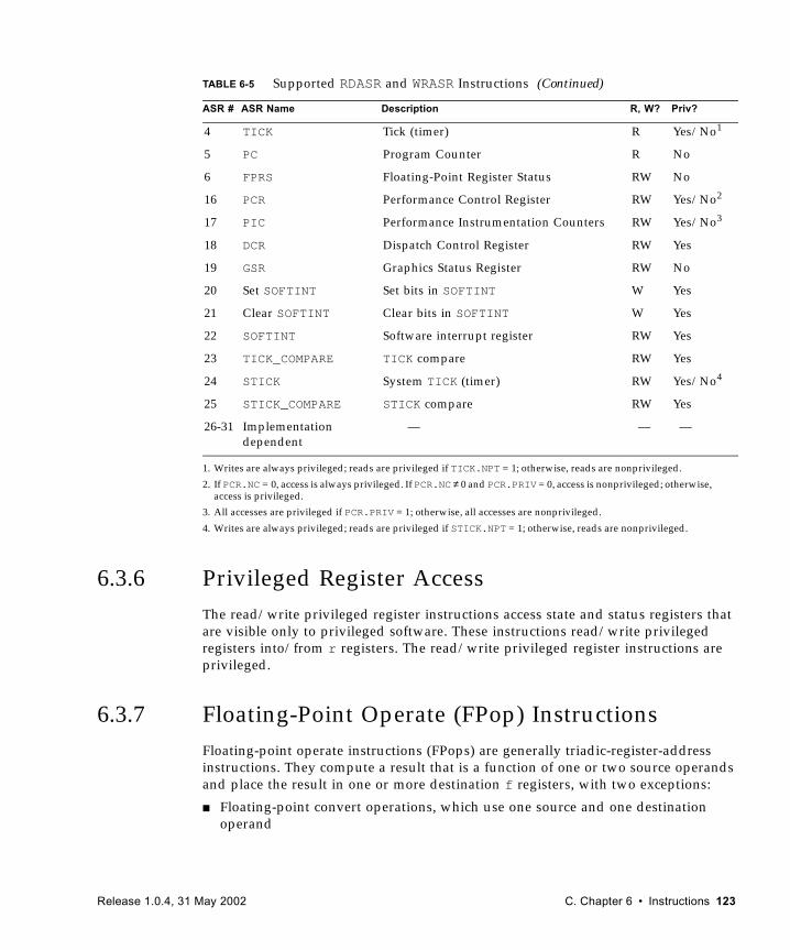
6.3.6 Privileged Register AccessThe read/write privileged register instructions access state and status registers that are visible only to privileged software. These instructions read/write privileged registers into/from r registers. The read/write privileged register instructions are privileged.
6.3.7 Floating-Point Operate (FPop) InstructionsFloating-point operate instructions (FPops) are generally triadic-register-address instructions. They compute a result that is a function of one or two source operands and place the result in one or more destination f registers, with two exceptions:
■ Floating-point convert operations, which use one source and one destination operand
4 TICK Tick (timer) R Yes/No1
5 PC Program Counter R No
6 FPRS Floating-Point Register Status RW No
16 PCR Performance Control Register RW Yes/No2
17 PIC Performance Instrumentation Counters RW Yes/No3
18 DCR Dispatch Control Register RW Yes
19 GSR Graphics Status Register RW No
20 Set SOFTINT Set bits in SOFTINT W Yes
21 Clear SOFTINT Clear bits in SOFTINT W Yes
22 SOFTINT Software interrupt register RW Yes
23 TICK_COMPARE TICK compare RW Yes
24 STICK System TICK (timer) RW Yes/No4
25 STICK_COMPARE STICK compare RW Yes
26-31 Implementation dependent
— — —
1. Writes are always privileged; reads are privileged if TICK.NPT = 1; otherwise, reads are nonprivileged.
2. If PCR.NC = 0, access is always privileged. If PCR.NC ≠ 0 and PCR.PRIV = 0, access is nonprivileged; otherwise,access is privileged.
3. All accesses are privileged if PCR.PRIV = 1; otherwise, all accesses are nonprivileged.
4. Writes are always privileged; reads are privileged if STICK.NPT = 1; otherwise, reads are nonprivileged.
TABLE 6-5 Supported RDASR and WRASR Instructions (Continued)
ASR # ASR Name Description R, W? Priv?
Release 1.0.4, 31 May 2002 C. Chapter 6 • Instructions 123
■ Floating-point compare operations, which do not write to an f register but update one of the fccn fields of the FSR instead
The term “FPop” refers to those instructions encoded by the FPop1 and FPop2 opcodes and does not include branches based on the floating-point condition codes (FBfcc and FBPfcc) or the load/store floating-point instructions.
The FMOVcc instructions function for the floating-point registers as the MOVcc instructions do for the integer registers. See MOVcc and FMOVcc Instructions on page 119.
The FMOVr instructions function for the floating-point registers as the MOVr instructions do for the integer registers. See MOVr and FMOVr Instructions on page 119.
If no floating-point unit is present or if PSTATE.PEF = 0 or FPRS.FEF = 0, then any instruction, including an FPop instruction, that attempts to access an FPU register generates an fp_disabled exception.
All FPop instructions clear the ftt field and set the cexc field unless they generate an exception. Floating-point compare instructions also write one of the fccn fields. All FPop instructions that can generate IEEE exceptions set the cexc and aexc fields unless they generate an exception. FABS(s,d,q), FMOV(s,d,q), FMOVcc(s,d,q), FMOVr(s,d,q), and FNEG(s,d,q) cannot generate IEEE exceptions, so they clear cexc and leave aexc unchanged.
IMPL. DEP. #3: An implementation may indicate that a floating-point instruction did not produce a correct IEEE Std 754-1985 result by generating an fp_exception_other exception with FSR.ftt = unfinished_FPop or unimplemented FPop. In this case, privileged software must emulate any functionality not present in the hardware.
SPARC JPS1 processors do not implement any quad-precision floating-point operations in hardware. Instead, these operations cause an fp_exception_other trap with FSR.ftt = unimplemented_FPop, and system software emulates quad operations (impl. dep. #1).
See ftt = unfinished_FPop on page 61 to see which instructions can produce an unfinished_FPop exception. See ftt = unimplemented_FPop on page 63 to see which instructions can produce an unimplemented_FPop exception.
6.3.8 Implementation-Dependent InstructionsSPARC V9 provides two instructions that are entirely implementation dependent: IMPDEP1 and IMPDEP2.
In SPARC JPS1, the IMPDEP1 opcode space is used by graphics instructions.
124 SPARC® Joint Programming Specification (JPS1): Commonality • Release 1.0.4, 31 May 2002
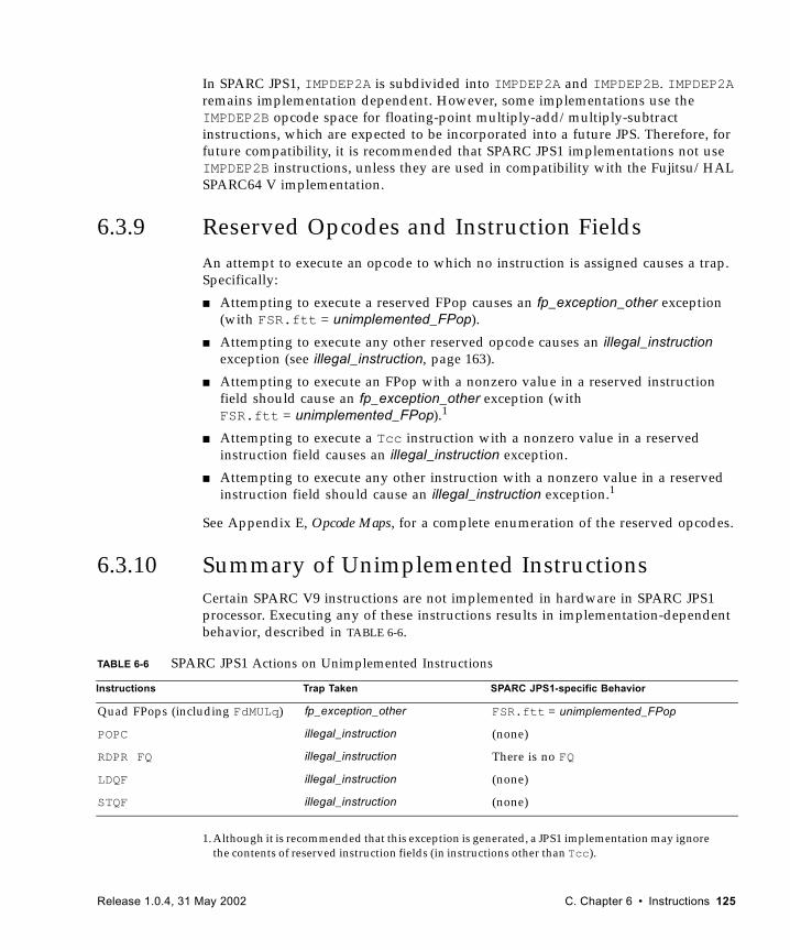
In SPARC JPS1, IMPDEP2A is subdivided into IMPDEP2A and IMPDEP2B. IMPDEP2A remains implementation dependent. However, some implementations use the IMPDEP2B opcode space for floating-point multiply-add/multiply-subtract instructions, which are expected to be incorporated into a future JPS. Therefore, for future compatibility, it is recommended that SPARC JPS1 implementations not use IMPDEP2B instructions, unless they are used in compatibility with the Fujitsu/HAL SPARC64 V implementation.
6.3.9 Reserved Opcodes and Instruction FieldsAn attempt to execute an opcode to which no instruction is assigned causes a trap. Specifically:
■ Attempting to execute a reserved FPop causes an fp_exception_other exception (with FSR.ftt = unimplemented_FPop).
■ Attempting to execute any other reserved opcode causes an illegal_instruction exception (see illegal_instruction, page 163).
■ Attempting to execute an FPop with a nonzero value in a reserved instruction field should cause an fp_exception_other exception (with FSR.ftt = unimplemented_FPop).1
■ Attempting to execute a Tcc instruction with a nonzero value in a reserved instruction field causes an illegal_instruction exception.
■ Attempting to execute any other instruction with a nonzero value in a reserved instruction field should cause an illegal_instruction exception.1
See Appendix E, Opcode Maps, for a complete enumeration of the reserved opcodes.
6.3.10 Summary of Unimplemented InstructionsCertain SPARC V9 instructions are not implemented in hardware in SPARC JPS1 processor. Executing any of these instructions results in implementation-dependent behavior, described in TABLE 6-6.
1. Although it is recommended that this exception is generated, a JPS1 implementation may ignore the contents of reserved instruction fields (in instructions other than Tcc).
TABLE 6-6 SPARC JPS1 Actions on Unimplemented Instructions
Instructions Trap Taken SPARC JPS1-specific Behavior
Quad FPops (including FdMULq) fp_exception_other FSR.ftt = unimplemented_FPop
POPC illegal_instruction (none)
RDPR FQ illegal_instruction There is no FQ
LDQF illegal_instruction (none)
STQF illegal_instruction (none)
Release 1.0.4, 31 May 2002 C. Chapter 6 • Instructions 125
Programming Note – The operating system emulates all of these instructions except RDPR FQ.
6.4 Register Window ManagementThe state of the register windows is determined by the contents of the set of privileged registers described in Register Window Management Instructions on page 120. Those registers are affected by the instructions described in Register Window Management on page 126. Privileged software can read/write these state registers directly by using RDPR/WRPR instructions.
6.4.1 Register Window State DefinitionFor the state of the register windows to be consistent, the following must always be true:
CANSAVE + CANRESTORE + OTHERWIN = NWINDOWS – 2
FIGURE 5-3 on page 45 shows how the register windows are partitioned to obtain the above equation. The partitions are as follows:
■ The current window and the window that overlaps two other valid windows and so must not be used (in FIGURE 5-3, windows 0 and 5, respectively). They are always present and account for the 2 subtracted from NWINDOWS in the right side of the equation.
■ Windows that do not have valid contents and can be used (through a SAVE instruction) without causing a spill trap. These windows (windows 1–4 in FIGURE 5-3) are counted in CANSAVE.
■ Windows that have valid contents for the current address space and that can be used (through the RESTORE instruction) without causing a fill trap. These windows (window 7 in FIGURE 5-3) are counted in CANRESTORE.
■ Windows that have valid contents for an address space other than the current address space. An attempt to use these windows through a SAVE (RESTORE) instruction results in a spill (fill) trap to a separate set of trap vectors, as discussed in the following subsection. These windows (window 6 in FIGURE 5-3) are counted in OTHERWIN.
126 SPARC® Joint Programming Specification (JPS1): Commonality • Release 1.0.4, 31 May 2002
In addition,
CLEANWIN ≥ CANRESTORE
since CLEANWIN is the sum of CANRESTORE and the number of clean windows following CWP.
For the window-management features of the architecture described in this section to be used, the state of the register windows must be kept consistent at all times, except within the trap handlers for window spilling, filling, and cleaning. While window traps are being handled, the state may be inconsistent. Window spill/fill trap handlers should be written so that a nested trap can be taken without destroying state.
Programming Note – System software is responsible for keeping the state of the register windows consistent at all times. Failure to do so will cause undefined behavior. For example, CANSAVE, CANRESTORE, and OTHERWIN must never be greater than or equal to 7 (NWINDOWS – 1).
6.4.2 Register Window TrapsWindow traps are used to manage overflow and underflow conditions in the register windows, support clean windows, and implement the FLUSHW instruction.
Window Spill and Fill Traps
A window overflow occurs when a SAVE instruction is executed and the next register window is occupied (CANSAVE = 0). An overflow causes a spill trap that allows privileged software to save the occupied register window in memory, thereby making it available for use.
A window underflow occurs when a RESTORE instruction is executed and the previous register window is not valid (CANRESTORE = 0). An underflow causes a fill trap that allows privileged software to load the registers from memory.
Clean-Window Trap
The processor provides the clean_window trap so that software can create a secure environment in which it is guaranteed that register windows contain only data from the same address space.
A clean register window is one in which all of the registers, including uninitialized registers, contain either 0 or data assigned by software executing in the address space to which the window belongs. A clean window cannot contain register values from another process, that is, software operating in a different address space.
Release 1.0.4, 31 May 2002 C. Chapter 6 • Instructions 127
Supervisor software specifies the number of windows that are clean with respect to the current address space in the CLEANWIN register. This number includes register windows that can be restored (the value in the CANRESTORE register) and the register windows following CWP that can be used without cleaning. Therefore, the number of clean windows that are available to be used by the SAVE instruction is
CLEANWIN – CANRESTORE
The SAVE instruction causes a clean_window exception if this value is 0. This behavior allows supervisor software to clean a register window before it is accessed by a user.
Vectoring of Fill/Spill Traps
To make handling of fill and spill traps efficient, SPARC V9 provides multiple trap vectors for the fill and spill traps. These trap vectors are determined as follows:
■ Supervisor software can mark a set of contiguous register windows as belonging to an address space different from the current one. The count of these register windows is kept in the OTHERWIN register. A separate set of trap vectors (fill_n_other and spill_n_other) is provided for spill and fill traps for these register windows (as opposed to register windows that belong to the current address space).
■ Supervisor software can specify the trap vectors for fill and spill traps by presetting the fields in the WSTATE register. This register contains two subfields, each three bits wide. The WSTATE.NORMAL field determines one of eight spill (fill) vectors to be used when the register window to be spilled (filled) belongs to the current address space (OTHERWIN = 0). If the OTHERWIN register is nonzero, the WSTATE.OTHER field selects one of eight fill_n_other (spill_n_other) trap vectors.
See Chapter 7, Traps, for more details on how the trap address is determined.
CWP on Window Traps
On a window trap, the CWP is set to point to the window that must be accessed by the trap handler, as follows. (Note: All arithmetic on CWP is done modulo NWINDOWS.)
■ If the spill trap occurs because of a SAVE instruction (when CANSAVE = 0), there is an overlap window between the CWP and the next register window to be spilled:
CWP ← (CWP + 2) mod NWINDOWS
If the spill trap occurs because of a FLUSHW instruction, there can be unused windows (CANSAVE) in addition to the overlap window between the CWP and the window to be spilled:
128 SPARC® Joint Programming Specification (JPS1): Commonality • Release 1.0.4, 31 May 2002
CWP ← (CWP + CANSAVE + 2) mod NWINDOWS
Implementation Note – All spill traps can useCWP ← (CWP + CANSAVE + 2) mod NWINDOWSsince CANSAVE is 0 whenever a trap occurs because of a SAVE instruction.
■ On a fill trap, the window preceding CWP must be filled:
CWP ← (CWP – 1) mod NWINDOWS
■ On a clean_window trap, the window following CWP must be cleaned. Then
CWP ← (CWP + 1) mod NWINDOWS
Window Trap Handlers
The trap handlers for fill, spill, and clean_window traps must handle the trap appropriately and return, by using the RETRY instruction, to reexecute the trapped instruction. The state of the register windows must be updated by the trap handler, and the relationships among CLEANWIN, CANSAVE, CANRESTORE, and OTHERWIN must remain consistent. Follow these recommendations:
■ A spill trap handler should execute the SAVED instruction for each window that it spills.
■ A fill trap handler should execute the RESTORED instruction for each window that it fills.
■ A clean_window trap handler should increment CLEANWIN for each window that it cleans:
CLEANWIN ← (CLEANWIN + 1)
Window trap handlers in SPARC JPS1 can be very efficient. See Example Code for Spill Handler on page 504 for details and sample code.
Release 1.0.4, 31 May 2002 C. Chapter 6 • Instructions 129

130 SPARC® Joint Programming Specification (JPS1): Commonality • Release 1.0.4, 31 May 2002
C.CHAPTER 7
Traps
A trap is a vectored transfer of control to supervisor software through a trap table that contains the first eight (32 for clean_window, spill, fill, fast_instruction_access_MMU_miss, fast_data_access_MMU_miss, and fast_data_access_protection traps) instructions of each trap handler. The base address of the table is established by supervisor software, by writing the Trap Base Address (TBA) register. The displacement within the table is determined by the trap type and the current trap level (TL). One-half of the table is reserved for hardware traps; one-quarter is reserved for software traps generated by Tcc instructions; the remaining quarter is reserved for future use.
A trap behaves like an unexpected procedure call. It causes the hardware to do the following:
1. Save certain processor state (program counters, CWP, ASI, CCR, PSTATE, and the trap type) on a hardware register stack.
2. Enter privileged execution mode with a predefined PSTATE.
3. Begin executing trap handler code in the trap vector.
When the trap handler has finished, it uses either a DONE or RETRY instruction to return.
A trap may be caused by a Tcc instruction, an instruction-induced exception, a reset, an asynchronous error, or an interrupt request not directly related to a particular instruction. The processor must appear to behave as though, before executing each instruction, it determines if there are any pending exceptions or interrupt requests. If there are pending exceptions or interrupt requests, the processor selects the highest-priority exception or interrupt request and causes a trap.
Thus, an exception is a condition that makes it impossible for the processor to continue executing the current instruction stream without software intervention. A trap is the action taken by the processor when it changes the instruction flow in response to the presence of an exception, interrupt, or Tcc instruction.
Release 1.0.4, 31 May 2002 C. Chapter 7 • Traps 131
A catastrophic error exception is due to the detection of a hardware malfunction from which, due to the nature of the error, the state of the machine at the time of the exception cannot be restored. Since the machine state cannot be restored, execution after such an exception may not be resumable. An example of such an error is an uncorrectable bus parity error.
IMPL. DEP. #31: The causes and effects of catastrophic errors are implementation-dependent. They may cause precise, deferred, or disrupting traps.
Traps are described in these sections:
■ Processor States, Normal and Special Traps on page 132■ Trap Categories on page 137■ Trap Control on page 140■ Trap-Table Entry Addresses on page 141■ Trap Processing on page 149■ Exception and Interrupt Descriptions on page 161
7.1 Processor States, Normal and Special TrapsThe processor is always in one of three discrete states:
■ execute_state, which is the normal execution state of the processor
■ RED_state (Reset, Error, and Debug state), which is a restricted execution state reserved for processing traps that occur when TL = MAXTL – 1, and for processing hardware- and software-initiated resets
■ error_state, which is a halted state that is entered as a result of a trap when TL = MAXTL
Traps processed in execute_state are called normal traps. Traps processed in RED_state are called special traps.
132 SPARC® Joint Programming Specification (JPS1): Commonality • Release 1.0.4, 31 May 2002
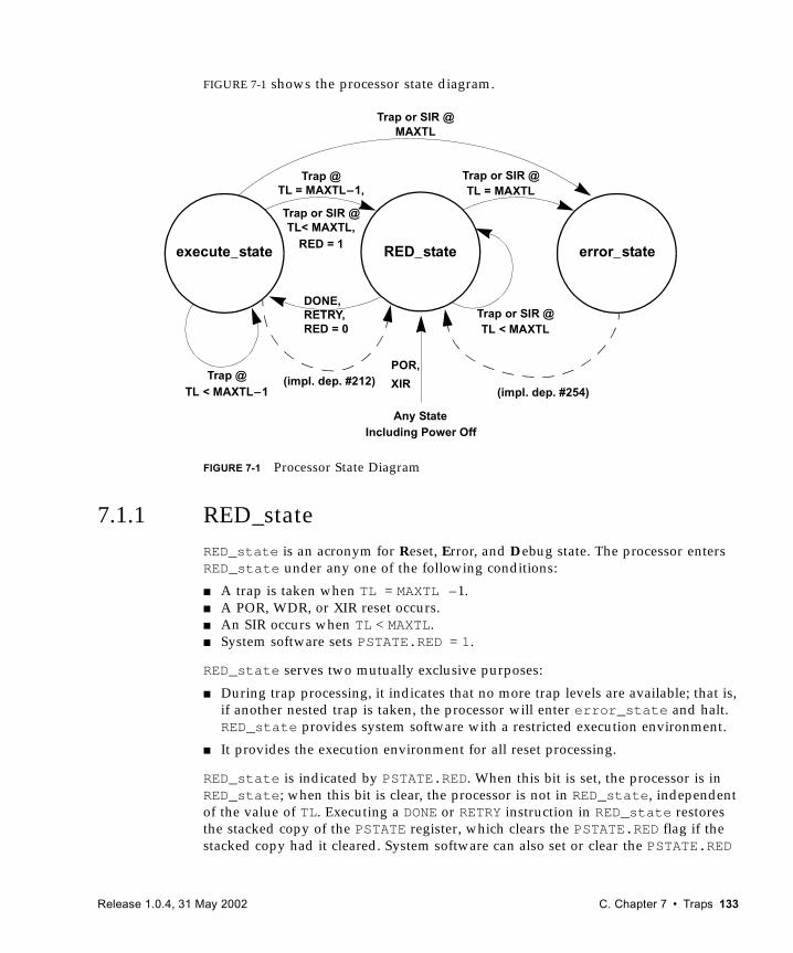
FIGURE 7-1 shows the processor state diagram.
FIGURE 7-1 Processor State Diagram
7.1.1 RED_stateRED_state is an acronym for Reset, Error, and Debug state. The processor enters RED_state under any one of the following conditions:
■ A trap is taken when TL = MAXTL –1.■ A POR, WDR, or XIR reset occurs.■ An SIR occurs when TL < MAXTL. ■ System software sets PSTATE.RED = 1.
RED_state serves two mutually exclusive purposes:
■ During trap processing, it indicates that no more trap levels are available; that is, if another nested trap is taken, the processor will enter error_state and halt. RED_state provides system software with a restricted execution environment.
■ It provides the execution environment for all reset processing.
RED_state is indicated by PSTATE.RED. When this bit is set, the processor is in RED_state; when this bit is clear, the processor is not in RED_state, independent of the value of TL. Executing a DONE or RETRY instruction in RED_state restores the stacked copy of the PSTATE register, which clears the PSTATE.RED flag if the stacked copy had it cleared. System software can also set or clear the PSTATE.RED
RED_stateexecute_state error_state
POR,
Including Power Off
Trap or SIR @
Trap or SIR @MAXTL
Trap @TL = MAXTL–1,
DONE,
TL = MAXTL
RED = 1
RED = 0
XIR
Any State
Trap or SIR @TL < MAXTL
Trap @TL < MAXTL–1
Trap or SIR @TL< MAXTL,
(impl. dep. #254)(impl. dep. #212)
RETRY,
Release 1.0.4, 31 May 2002 C. Chapter 7 • Traps 133
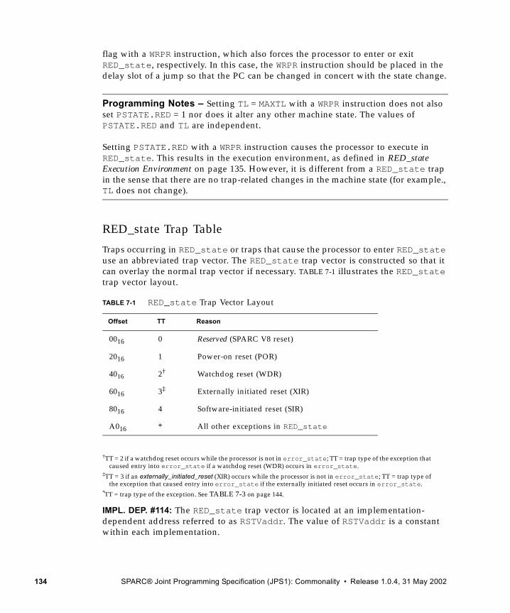
flag with a WRPR instruction, which also forces the processor to enter or exit RED_state, respectively. In this case, the WRPR instruction should be placed in the delay slot of a jump so that the PC can be changed in concert with the state change.
Programming Notes – Setting TL = MAXTL with a WRPR instruction does not also set PSTATE.RED = 1 nor does it alter any other machine state. The values of PSTATE.RED and TL are independent.
Setting PSTATE.RED with a WRPR instruction causes the processor to execute in RED_state. This results in the execution environment, as defined in RED_state Execution Environment on page 135. However, it is different from a RED_state trap in the sense that there are no trap-related changes in the machine state (for example., TL does not change).
RED_state Trap Table
Traps occurring in RED_state or traps that cause the processor to enter RED_state use an abbreviated trap vector. The RED_state trap vector is constructed so that it can overlay the normal trap vector if necessary. TABLE 7-1 illustrates the RED_state trap vector layout.
†TT = 2 if a watchdog reset occurs while the processor is not in error_state; TT = trap type of the exception thatcaused entry into error_state if a watchdog reset (WDR) occurs in error_state.
‡TT = 3 if an externally_initiated_reset (XIR) occurs while the processor is not in error_state; TT = trap type ofthe exception that caused entry into error_state if the externally initiated reset occurs in error_state.
*TT = trap type of the exception. See TABLE 7-3 on page 144.
IMPL. DEP. #114: The RED_state trap vector is located at an implementation-dependent address referred to as RSTVaddr. The value of RSTVaddr is a constant within each implementation.
TABLE 7-1 RED_state Trap Vector Layout
Offset TT Reason
0016 0 Reserved (SPARC V8 reset)
2016 1 Power-on reset (POR)
4016 2† Watchdog reset (WDR)
6016 3‡ Externally initiated reset (XIR)
8016 4 Software-initiated reset (SIR)
A016 * All other exceptions in RED_state
134 SPARC® Joint Programming Specification (JPS1): Commonality • Release 1.0.4, 31 May 2002
RED_state Execution Environment
In RED_state, the processor is forced to execute in a restricted environment by overriding the values of some processor controls and state registers.
The values are overridden, not set, allowing them to be switched atomically.
IMPL. DEP. #115: A processor’s behavior in RED_state is implementation dependent.
When RED_state is entered because of component failures, the handler should attempt to recover from potentially catastrophic error conditions or to disable the failing components. When RED_state is entered after a reset, the software should create the environment necessary to restore the system to a running state.
RED_state Entry Traps
The following traps are processed in RED_state in all cases.
■ Power-on reset (POR) — Implemented in hardware in SPARC JPS1 processors; not really a trap.
■ Watchdog reset (WDR) — Implemented in hardware in SPARC JPS1; this trap is used as a recovery mechanism from error_state in SPARC JPS1. Upon an entry to error_state, the processor automatically invokes a watchdog reset to enter RED_state.
■ Externally initiated reset (XIR) — Implemented in hardware in SPARC JPS1; typically used as a nonmaskable interrupt method for debug.
In addition, the following trap is processed in RED_state if TL < MAXTL when the trap is taken. Otherwise, it is processed in error_state.
■ Software-initiated reset (SIR)
Traps that occur when TL = MAXTL – 1 also set PSTATE.RED = 1; that is, any trap handler entered with TL = MAXTL runs in RED_state.
Any non-reset trap that sets PSTATE.RED = 1 or that occurs when PSTATE.RED = 1 branches to a special entry in the RED_state trap vector at RSTVaddr + A016.
RED_state Software Considerations
In effect, RED_state reserves one level of the trap stack for recovery and reset processing. Software should be designed to require only MAXTL – 1 trap levels for normal processing. That is, any trap that causes TL = MAXTL is an exceptional condition that should cause entry to RED_state.
Release 1.0.4, 31 May 2002 C. Chapter 7 • Traps 135
The architected value for MAXTL in SPARC JPS1 is 5; typical usage of the trap levels is shown in TABLE 7-2.
Programming Note – To log the state of the processor, RED_state-handler software needs either a spare register or a preloaded pointer to a save area. To support recovery, the operating system might reserve one of the alternate global registers (for example, %a7) for use in RED_state.
7.1.2 Error_stateThe processor enters error_state when a trap occurs while the processor is already at its maximum supported trap level, that is, when TL = MAXTL.
IMPL. DEP. #39: The processor may enter error_state when an implementation dependent error condition occurs.
IMPL. DEP. #40: Effects when error_state is entered are implementation-dependent, but it is recommended that as much processor state as possible be preserved upon entry to error_state. In addition, a SPARC JPS1 processor may have other error_state entry traps that are implementation dependent.
IMPL. DEP. #254: The means of exiting error_state are implementation dependent. A suggested method is for the processor, upon entering error_state, to automatically generate a watchdog_reset (WDR).
TABLE 7-2 Typical Usage for Trap Levels
TL Usage
0 Normal execution
1 System calls; interrupt handlers; instruction emulation
2 Window spill/fill
3 Page-fault handler
4 Reserved for error handling
5 RED_state handler
136 SPARC® Joint Programming Specification (JPS1): Commonality • Release 1.0.4, 31 May 2002
7.2 Trap CategoriesAn exception or interrupt request can cause any of the following trap types:
■ Precise trap■ Deferred trap■ Disrupting trap■ Reset trap
7.2.1 Precise TrapsA precise trap is induced by a particular instruction and occurs before any program-visible state has been changed by the trap-inducing instructions. When a precise trap occurs, several conditions must be true.
■ The PC saved in TPC[TL] points to the instruction that induced the trap and the nPC saved in TNPC[TL] points to the instruction that was to be executed next.
■ All instructions issued before the one that induced the trap have completed execution.
■ Any instructions issued after the one that induced the trap remain unexecuted.
Among the actions the trap handler software might take after a precise trap are these:
■ Return to the instruction that caused the trap and reexecute it by executing a RETRY instruction (PC ← old PC, nPC ← old nPC).
■ Emulate the instruction that caused the trap and return to the succeeding instruction by executing a DONE instruction (PC ← old nPC, nPC← old nPC + 4).
■ Terminate the program or process associated with the trap.
7.2.2 Deferred TrapsA deferred trap is also induced by a particular instruction, but unlike a precise trap, a deferred trap may occur after program-visible state has been changed. Such state may have been changed by the execution of either the trap-inducing instruction itself or by one or more other instructions.
Associated with a particular deferred-trap implementation, the following must exist:
■ An instruction that causes a potentially outstanding deferred-trap exception to be taken as a trap
■ Privileged instructions that access the state information needed by the supervisor software to emulate the deferred-trap-inducing instruction and to resume execution of the trapped instruction stream
Release 1.0.4, 31 May 2002 C. Chapter 7 • Traps 137
Programming Note – Resuming execution may require the emulation of instructions that had not completed execution at the time of the deferred trap, that is, those instructions in the deferred-trap queue.
IMPL. DEP. #32: Whether any deferred traps (and, possibly, associated deferred-trap queues) are present is implementation dependent.
Among the actions software can take after a deferred trap are these:
■ Emulate the instruction that caused the exception, emulate or cause to execute any other execution-deferred instructions that were in an associated deferred-trap state queue, and use RETRY to return control to the instruction at which the deferred trap was invoked.
■ Terminate the program or process associated with the trap.
7.2.3 Disrupting TrapsA disrupting trap is neither a precise trap nor a deferred trap. A disrupting trap is caused by a condition (for example, an interrupt) rather than directly by a particular instruction; that cause distinguishes it from precise and deferred traps. When a disrupting trap has been serviced, trap handler software normally arranges for program execution to resume where it left off. That differentiates disrupting traps from reset traps, which trap to a unique reset address from which execution of the program that was running when the reset occurred is never expected to resume.
Disrupting traps are controlled by a combination of the Processor Interrupt Level (PIL) register and the Interrupt Enable (IE) field of PSTATE. A disrupting trap condition is ignored when interrupts are disabled (PSTATE.IE = 0) or when the condition’s interrupt level is less than or equal to that specified in PIL.
A disrupting trap may be due either to an interrupt request not directly related to a previously executed instruction or to an exception related to a previously executed instruction. Interrupt requests may be either internal or external. An interrupt request can be induced by the assertion of a signal not directly related to any particular processor or memory state, for example, the assertion of an “I/O done” signal.
A disrupting trap related to an earlier instruction causing an exception is similar to a deferred trap in that it occurs after instructions following the trap-inducing instruction have modified the processor or memory state. The difference is that the condition that caused the instruction to induce the disrupting trap may lead to unrecoverable errors, since the implementation may not preserve the necessary state. An example is an ECC data-access error reported after the corresponding load instruction has completed.
Disrupting trap conditions should persist until the corresponding trap is taken.
138 SPARC® Joint Programming Specification (JPS1): Commonality • Release 1.0.4, 31 May 2002
Among the actions that trap-handler software might take after a disrupting trap are these:
■ Use RETRY to return to the instruction at which the trap was invoked(PC ← old PC, nPC ← old nPC).
■ Terminate the program or process associated with the trap.
7.2.4 Reset TrapsA reset trap occurs when supervisor software or the implementation’s hardware determines that the machine must be reset to a known state. Reset traps differ from disrupting traps in that trap handler software for resets is never expected to resume execution of the program that was running when the reset trap occurred.
IMPL. DEP. #37: Some of a processor’s behavior during a reset trap is implementation dependent. See Special Trap Processing on page 155 for details.
The following reset traps are defined for SPARC V9:
■ Software-initiated reset (SIR) — Initiated by software by executing the SIR instruction.
■ Power-on reset (POR) — Initiated when power is applied (or reapplied) to the processor.
■ Watchdog reset (WDR) — Initiated in response to watchdog timer overflow or entry into error_state (impl. dep. #254).
■ Externally initiated reset (XIR) — Initiated in response to an external signal. This reset trap is normally used for critical system events, such as power failure.
7.2.5 Uses of the Trap CategoriesThe SPARC V9 trap model makes the following stipulations:
1. Reset traps, except software_initiated_reset traps, occur asynchronously to program execution.
2. When recovery from an exception can affect the interpretation of subsequent instructions, such exceptions shall be precise. These exceptions are:■ software_initiated_reset■ instruction_access_exception■ privileged_action■ privileged_opcode■ trap_instruction■ instruction_access_error■ clean_window■ fp_disabled■ LDDF_mem_address_not_aligned
Release 1.0.4, 31 May 2002 C. Chapter 7 • Traps 139
■ STDF_mem_address_not_aligned■ LDQF_mem_address_not_aligned (not used in SPARC JPS1)■ STQF_mem_address_not_aligned (not used in SPARC JPS1)■ tag_overflow■ spill_n_normal■ spill_n_other■ fill_n_normal■ fill_n_other
3. IMPL. DEP. #33: Exceptions that occur as the result of program execution may be precise or deferred, although it is recommended that such exceptions be precise. Examples are mem_address_not_aligned, division_by_zero.
4. An exception caused after the initial access of a multiple-access load or store instruction (load/store doubleword, block load, block store, LDSTUB, CASA, CASXA, or SWAP) that causes a catastrophic exception may be precise, deferred, or disrupting. Thus, a trap due to the second memory access can occur after the processor or memory state has been modified by the first access.
5. Implementation-dependent catastrophic exceptions may cause precise, deferred, or disrupting traps (impl. dep. #31).
6. Exceptions caused by external events unrelated to the instruction stream, such as interrupts, are disrupting.
A deferred trap may occur one or more instructions after the trap-inducing instruction is dispatched.
7.3 Trap ControlSeveral registers control how any given trap is processed:
■ The interrupt enable (IE) field in PSTATE and the processor interrupt level (PIL) register control interrupt processing.
■ The enable floating-point unit (FEF) field in FPRS, the floating-point unit enable (PEF) field in PSTATE, and the trap enable mask (TEM) in the FSR control floating-point traps.
■ The TL register, which contains the current level of trap nesting, controls whether a trap causes entry to execute_state, RED_state, or error_state.
■ PSTATE.TLE determines whether implicit data accesses in the trap routine will be performed with the big- or little-endian byte order.
140 SPARC® Joint Programming Specification (JPS1): Commonality • Release 1.0.4, 31 May 2002
7.3.1 PIL ControlBetween the execution of instructions, the IU prioritizes the outstanding exceptions and interrupt requests. At any given time, only the highest priority exception or interrupt request is taken as a trap. When there are multiple outstanding exceptions or interrupt requests, SPARC V9 assumes that lower-priority interrupt requests will persist and lower-priority exceptions will recur if an exception-causing instruction is reexecuted.
For interrupt requests, the IU compares the interrupt request level against the processor interrupt level (PIL) register. If the interrupt request level is greater than PIL, then the processor takes the interrupt request trap, assuming there are no higher-priority exceptions outstanding.
IMPL. DEP. #34: How quickly a processor responds to an interrupt request and the method by which an interrupt request is removed are implementation dependent.
7.3.2 TEM ControlThe occurrence of floating-point traps of type IEEE_754_exception can be controlled with the user-accessible trap enable mask (TEM) field of the FSR. If a particular bit of TEM is 1, the associated IEEE_754_exception can cause an fp_exception_ieee_754 trap.
If a particular bit of TEM is 0, the associated IEEE_754_exception does not cause an fp_exception_ieee_754 trap. Instead, the occurrence of the exception is recorded in the FSR’s accrued exception field (aexc).
If an IEEE_754_exception results in an fp_exception_ieee_754 trap, then the destination f register, fccn, and aexc fields remain unchanged. However, if an IEEE_754_exception does not result in a trap, then the f register, fccn, and aexc fields are updated to their new values.
7.4 Trap-Table Entry AddressesPrivileged software initializes the trap base address (TBA) register to the upper 49 bits of the trap-table base address. Bit 14 of the vector address (the TL>0 field) is set based on the value of TL at the time the trap is taken; that is, to 0 if TL = 0 and to 1
Release 1.0.4, 31 May 2002 C. Chapter 7 • Traps 141
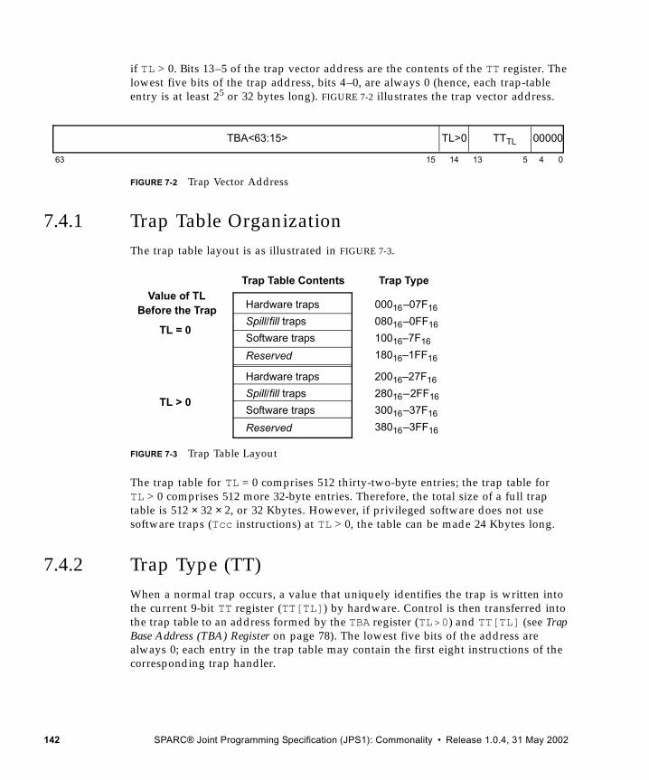
if TL > 0. Bits 13–5 of the trap vector address are the contents of the TT register. The lowest five bits of the trap address, bits 4–0, are always 0 (hence, each trap-table entry is at least 25 or 32 bytes long). FIGURE 7-2 illustrates the trap vector address.
FIGURE 7-2 Trap Vector Address
7.4.1 Trap Table OrganizationThe trap table layout is as illustrated in FIGURE 7-3.
FIGURE 7-3 Trap Table Layout
The trap table for TL = 0 comprises 512 thirty-two-byte entries; the trap table for TL > 0 comprises 512 more 32-byte entries. Therefore, the total size of a full trap table is 512 × 32 × 2, or 32 Kbytes. However, if privileged software does not use software traps (Tcc instructions) at TL > 0, the table can be made 24 Kbytes long.
7.4.2 Trap Type (TT)When a normal trap occurs, a value that uniquely identifies the trap is written into the current 9-bit TT register (TT[TL]) by hardware. Control is then transferred into the trap table to an address formed by the TBA register (TL>0) and TT[TL] (see Trap Base Address (TBA) Register on page 78). The lowest five bits of the address are always 0; each entry in the trap table may contain the first eight instructions of the corresponding trap handler.
63 15 14 0
TBA<63:15>
13 45
TL>0 TTTL 00000
Value of TLBefore the Trap
Trap Table Contents Trap Type
TL = 0
Hardware traps
Spill/fill traps
Software traps
Reserved
00016–07F16
08016–0FF16
10016–7F16
18016–1FF16
TL > 0
Hardware traps
Spill/fill traps
Software traps
Reserved
20016–27F16
28016–2FF16
30016–37F16
38016–3FF16
142 SPARC® Joint Programming Specification (JPS1): Commonality • Release 1.0.4, 31 May 2002
Programming Notes – The trap type for the clean_window exception is 02416. Three subsequent trap vectors (02516–02716) are reserved to allow for an inline (branchless) trap handler. Three subsequent trap vectors are reserved for each spill/fill vector, to allow for an inline (branchless) trap handler.
The spill/fill, clean_window, and MMU-related traps (fast_instruction_access_MMU_miss, fast_data_access_MMU_miss, and fast_data_access_protection) trap types are spaced such that their trap-table entries are 128 bytes (32 instructions) long in SPARC JPS1. This length allows the complete code for one spill/fill routine, a clean_window routine, or a normal MMU miss handling routine to reside in one trap-table entry.
When a special trap occurs, the TT register is set as described in RED_state on page 133. Control is then transferred into the RED_state trap table to an address formed by the RSTVaddr and an offset depending on the condition.
TT values 00016–0FF16 are reserved for hardware traps. TT values 10016–17F16 are reserved for software traps (traps caused by execution of a Tcc instruction). TT values 18016–1FF16 are reserved for future uses.
IMPL. DEP. #35: TT values 06016 to 07F16 are reserved for implementation-dependent exceptions. The existence of implementation_dependent_n traps and whether any that do exist are precise, deferred, or disrupting is implementation dependent. TT values 06016 through 06F16 are defined for JPS1 processors and 07016 through 07F16 remain implemenation-dependent; see TABLE 7-3 and Appendix C, Implementation Dependencies.
The assignment of TT values to traps is shown in TABLE 7-3; TABLE 7-4 lists the traps in priority order. Traps marked with an open bullet (❍ ) are optional and possibly implementation dependent. Traps marked with a closed bullet (● ) are mandatory; that is, hardware must detect and trap these exceptions and interrupts and must set the defined TT values. In the table, AG = alternate globals, MG = MMU globals, and IG = interrupt globals. “-NA-” means “not applicable”.
Release 1.0.4, 31 May 2002 C. Chapter 7 • Traps 143
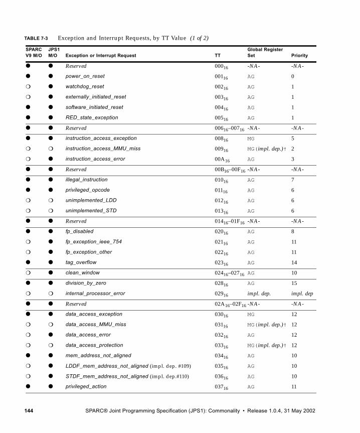
TABLE 7-3 Exception and Interrupt Requests, by TT Value (1 of 2)
SPARCV9 M/O
JPS1 M/O Exception or Interrupt Request TT
Global Register Set Priority
● ● Reserved 00016 -NA- -NA-
● ● power_on_reset 00116 AG 0
❍ ● watchdog_reset 00216 AG 1
❍ ● externally_initiated_reset 00316 AG 1
● ● software_initiated_reset 00416 AG 1
● ● RED_state_exception 00516 AG 1
● ● Reserved 00616–00716 -NA- -NA-
● ● instruction_access_exception 00816 MG 5
❍ ❍ instruction_access_MMU_miss 00916 MG(impl. dep.)† 2
❍ ● instruction_access_error 00A16 AG 3
● ● Reserved 00B16–00F16 -NA- -NA-
● ● illegal_instruction 01016 AG 7
● ● privileged_opcode 01116 AG 6
❍ ❍ unimplemented_LDD 01216 AG 6
❍ ❍ unimplemented_STD 01316 AG 6
● ● Reserved 01416–01F16 -NA- -NA-
● ● fp_disabled 02016 AG 8
❍ ● fp_exception_ieee_754 02116 AG 11
❍ ● fp_exception_other 02216 AG 11
● ● tag_overflow 02316 AG 14
❍ ● clean_window 02416–02716 AG 10
● ● division_by_zero 02816 AG 15
❍ ❍ internal_processor_error 02916 impl. dep. impl. dep
● ● Reserved 02A16–02F16 -NA- -NA-
● ● data_access_exception 03016 MG 12
❍ ❍ data_access_MMU_miss 03116 MG(impl. dep.)† 12
❍ ● data_access_error 03216 AG 12
❍ ❍ data_access_protection 03316 MG(impl. dep.)† 12
● ● mem_address_not_aligned 03416 AG 10
❍ ● LDDF_mem_address_not_aligned (impl. dep. #109) 03516 AG 10
❍ ● STDF_mem_address_not_aligned (impl. dep.#110) 03616 AG 10
● ● privileged_action 03716 AG 11
144 SPARC® Joint Programming Specification (JPS1): Commonality • Release 1.0.4, 31 May 2002
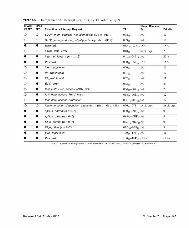
❍ ❍ LDQF_mem_address_not_aligned (impl. dep. #111) 03816 AG 10
❍ ❍ STQF_mem_address_not_aligned (impl. dep. #112) 03916 AG 10
● ● Reserved 03A16–03F16 -NA- -NA-
❍ ❍ async_data_error 04016 impl. dep. 2
● ● interrupt_level_n (n = 1–15) 04116–04F16 AG 32-n
● ● Reserved 05016–05F16 -NA- -NA-
❍ ● interrupt_vector 06016 IG 16
❍ ● PA_watchpoint 06116 AG 12
❍ ● VA_watchpoint 06216 AG 11
❍ ● ECC_error 06316 AG 33
❍ ● fast_instruction_access_MMU_miss 06416–06716 MG 2
❍ ● fast_data_access_MMU_miss 06816–06B16 MG 12
❍ ● fast_data_access_protection 06C16–06F16 MG 12
❍ ❍ implementation_dependent_exception_n (impl. dep. #35) 07016–07F impl. dep. impl. dep.
● ● spill_n_normal (n = 0–7) 08016–09F16 AG 9
● ● spill_n_other (n = 0–7) 0A016–0BF16AG 9
● ● fill_n_normal (n = 0–7) 0C016–0DF16AG 9
● ● fill_n_other (n = 0–7) 0E016–0FF16 AG 9
● ● trap_instruction 10016–17F16 AG 16
● ● Reserved 18016–1FF16 -NA- -NA-
† Global register set is implementation-dependent, but use of MMU Globals (MG) is recommended
TABLE 7-3 Exception and Interrupt Requests, by TT Value (2 of 2)
SPARCV9 M/O
JPS1 M/O Exception or Interrupt Request TT
Global Register Set Priority
Release 1.0.4, 31 May 2002 C. Chapter 7 • Traps 145
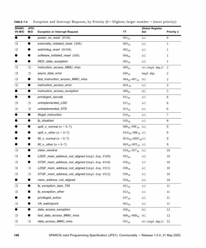
TABLE 7-4 Exception and Interrupt Requests, by Priority (0 = Highest; larger number = lower priority)
SPARCV9 M/O
JPS1M/O Exception or Interrupt Request TT
Global Register Set Priority ‡
● ● power_on_reset (POR) 00116 AG 0
❍ ● externally_initiated_reset (XIR) 00316 AG 1
❍ ● watchdog_reset (WDR) 00216 AG 1
● ● software_initiated_reset (SIR) 00416 AG 1
● ● RED_state_exception 00516 AG 1
❍ ❍ instruction_access_MMU_miss 00916 MG(impl. dep.)† 2
❍ ❍ async_data_error 04016 impl. dep. 2
❍ ● fast_instruction_access_MMU_miss 06416–06716 MG 2
❍ ● instruction_access_error 00A16 AG 3
● ● instruction_access_exception 00816 MG 5
● ● privileged_opcode 01116 AG 6
❍ ❍ unimplemented_LDD 01216 AG 6
❍ ❍ unimplemented_STD 01316 AG 6
● ● illegal_instruction 01016 AG 7
● ● fp_disabled 02016 AG 8
● ● spill_n_normal (n = 0–7) 08016–09F16 AG 9
● ● spill_n_other (n = 0–7) 0A016–0BF16 AG 9
● ● fill_n_normal (n = 0–7) 0C016–0DF16AG 9
● ● fill_n_other (n = 0–7) 0E016–0FF16 AG 9
❍ ● clean_window 02416–02716 AG 10
❍ ● LDDF_mem_address_not_aligned (impl. dep. #109) 03516 AG 10
❍ ● STDF_mem_address_not_aligned (impl. dep. #110) 03616 AG 10
❍ ❍ LDQF_mem_address_not_aligned (impl. dep. #111) 03816 AG 10
❍ ❍ STQF_mem_address_not_aligned (impl. dep. #112) 03916 AG 10
● ● mem_address_not_aligned 03416 AG 10
❍ ● fp_exception_ieee_754 02116 AG 11
❍ ● fp_exception_other 02216 AG 11
● ● privileged_action 03716 AG 11
❍ ● VA_watchpoint 06216 AG 11
● ● data_access_exception 03016 MG 12
❍ ● fast_data_access_MMU_miss 06816–06B16 MG 12
❍ ❍ data_access_MMU_miss 03116 MG(impl. dep.)† 12
146 SPARC® Joint Programming Specification (JPS1): Commonality • Release 1.0.4, 31 May 2002
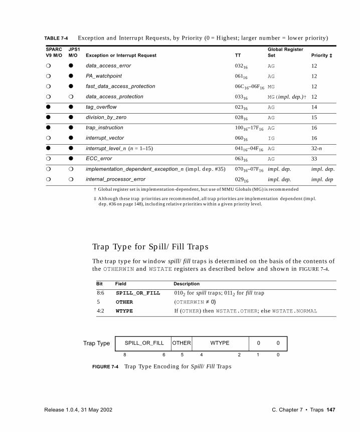
Trap Type for Spill/Fill Traps
The trap type for window spill/fill traps is determined on the basis of the contents of the OTHERWIN and WSTATE registers as described below and shown in FIGURE 7-4.
FIGURE 7-4 Trap Type Encoding for Spill/Fill Traps
❍ ● data_access_error 03216 AG 12
❍ ● PA_watchpoint 06116 AG 12
❍ ● fast_data_access_protection 06C16–06F16 MG 12
❍ ❍ data_access_protection 03316 MG(impl. dep.)† 12
● ● tag_overflow 02316 AG 14
● ● division_by_zero 02816 AG 15
● ● trap_instruction 10016–17F16 AG 16
❍ ● interrupt_vector 06016 IG 16
● ● interrupt_level_n (n = 1–15) 04116–04F16 AG 32-n
❍ ● ECC_error 06316 AG 33
❍ ❍ implementation_dependent_exception_n (impl. dep. #35) 07016–07F16 impl. dep. impl. dep.
❍ ❍ internal_processor_error 02916 impl. dep. impl. dep
† Global register set is implementation-dependent, but use of MMU Globals (MG) is recommended
‡ Although these trap priorities are recommended, all trap priorities are implementation dependent (impl. dep. #36 on page 148), including relative priorities within a given priority level.
Bit Field Description
8:6 SPILL_OR_FILL 0102 for spill traps; 0112 for fill trap
5 OTHER (OTHERWIN ≠ 0)4:2 WTYPE If (OTHER) then WSTATE.OTHER; else WSTATE.NORMAL
TABLE 7-4 Exception and Interrupt Requests, by Priority (0 = Highest; larger number = lower priority)
SPARCV9 M/O
JPS1M/O Exception or Interrupt Request TT
Global Register Set Priority ‡
Trap Type
05 2
0SPILL_OR_FILL
1468
0WTYPEOTHER
Release 1.0.4, 31 May 2002 C. Chapter 7 • Traps 147
7.4.3 Trap PrioritiesTABLE 7-3 on page 144 and TABLE 7-4 on page 146 show the assignment of traps to TT values and the relative priority of traps and interrupt requests. Priority 0 is highest and greater priority numbers indicate lower priority; that is, if X < Y, a pending exception or interrupt request with priority X is taken instead of a pending exception or interrupt request with priority Y.
IMPL. DEP. #36: The priorities of particular traps are relative and are implementation dependent, because a future version of the architecture may define new traps, and an implementation may define implementation-dependent traps that establish new relative priorities.
However, the TT values for the exceptions and interrupt requests shown in TABLE 7-3 and TABLE 7-4 must remain the same for every implementation.
The trap priorities given above always need to be considered in light of how the processor actually issues and executes instructions. For example, if an instruction_access_error occurs (priority 3), it will be taken even if the instruction was an SIR (priority 1). This situation occurs because the processor gets the instruction_access_error during instruction fetch and never actually issues or executes the instruction, so the SIR instruction is never seen by the execution units of the processor. This is an obvious case, but there are other more subtle cases.
In summary, the trap priorities are used to prioritize traps that occur in the same clock cycle. They do not take into consideration that an instruction may be alive for multiple cycles and that a trap may be detected and initiated early in the life of an instruction. Once the early trap is taken, any errors that might have occurred later in the instruction’s life will not be seen.
7.4.4 Details of Supported Traps
MMU Traps
SPARC JPS1 supports three 32-instruction traps for handling the most performance sensitive MMU traps:■ fast_instruction_access_MMU_miss■ fast_data_access_MMU_miss■ fast_data_access_protection
The first two traps are taken when the TLBs miss on an instruction or data access. The third type of trap is taken when a protection violation occurs. The common case of this trap occurs when a write request is made to a page marked as clean in the TLB.
148 SPARC® Joint Programming Specification (JPS1): Commonality • Release 1.0.4, 31 May 2002
Each of these trap vectors takes up 4 slots in the trap table; this means that each trap handler can contain up to 32 instructions before a branch is needed.
Other SPARC JPS1 Implementation-Specific Traps
SPARC JPS1 supports the following trap types in addition to those in SPARC V9:■ interrupt_vector_trap■ PA_watchpoint■ VA_watchpoint■ ECC_error
Unimplemented SPARC V9 Traps in SPARC JPS1■ instruction_access_MMU_miss■ unimplemented_LDD■ unimplemented_STD■ data_access_MMU_miss■ data_access_protection■ async_data_error■ LDQF_mem_address_not_aligned■ STQF_mem_address_not_aligned
7.5 Trap ProcessingThe processor’s action during trap processing depends on the trap type, the current level of trap nesting (given in the TL register), and the processor state. When a trap occurs, the global registers are replaced with one of three sets of trap global register—MMU globals, interrupt globals, or alternate globals—based on the type of trap.
All traps use normal trap processing, except those due to reset requests, catastrophic errors, traps taken when TL = MAXTL – 1, and traps taken when the processor is in RED_state. These traps use special RED_state trap processing.
During normal operation, the processor is in execute_state. It processes traps in execute_state and continues.
When a normal trap or software-initiated reset (SIR) occurs with TL = MAXTL, there are no more levels on the trap stack, so the processor enters error_state and halts. To avoid this catastrophic failure, SPARC V9 provides the RED_state processor state. Traps processed in RED_state use a special trap vector and a special trap-vectoring algorithm. RED_state vectoring and the setting of the TT value for RED_state traps are described in RED_state Trap Table on page 134.
Release 1.0.4, 31 May 2002 C. Chapter 7 • Traps 149
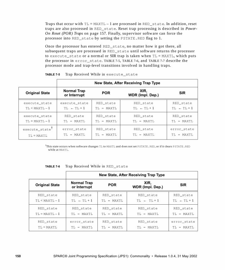
Traps that occur with TL = MAXTL – 1 are processed in RED_state. In addition, reset traps are also processed in RED_state. Reset trap processing is described in Power-On Reset (POR) Traps on page 157. Finally, supervisor software can force the processor into RED_state by setting the PSTATE.RED flag to 1.
Once the processor has entered RED_state, no matter how it got there, all subsequent traps are processed in RED_state until software returns the processor to execute_state or a normal or SIR trap is taken when TL = MAXTL, which puts the processor in error_state. TABLE 7-5, TABLE 7-6, and TABLE 7-7 describe the processor mode and trap-level transitions involved in handling traps.
†This state occurs when software changes TL to MAXTL and does not set PSTATE.RED, or if it clears PSTATE.REDwhile at MAXTL.
TABLE 7-5 Trap Received While in execute_state
New State, After Receiving Trap Type
Original State Normal Trapor Interrupt POR XIR,
WDR (Impl. Dep.) SIR
execute_state
TL < MAXTL – 1execute_state
TL ← TL + 1RED_state
TL = MAXTL
RED_state
TL ← TL + 1RED_state
TL ← TL + 1
execute_state
TL = MAXTL – 1RED_state
TL = MAXTL
RED_state
TL = MAXTL
RED_state
TL = MAXTL
RED_state
TL = MAXTL
execute_state†
TL = MAXTL
error_state
TL = MAXTL
RED_state
TL = MAXTL
RED_state
TL = MAXTL
error_state
TL = MAXTL
TABLE 7-6 Trap Received While in RED_state
New State, After Receiving Trap Type
Original State Normal Trapor Interrupt POR XIR,
WDR (Impl. Dep.) SIR
RED_state
TL < MAXTL – 1
RED_state
TL ← TL + 1
RED_state
TL = MAXTL
RED_state
TL ← TL + 1
RED_state
TL ← TL + 1
RED_state
TL = MAXTL – 1
RED_state
TL = MAXTL
RED_state
TL = MAXTL
RED_state
TL = MAXTL
RED_state
TL = MAXTL
RED_state
TL = MAXTL
error_state
TL = MAXTL
RED_state
TL = MAXTL
RED_state
TL = MAXTL
error_state
TL = MAXTL
150 SPARC® Joint Programming Specification (JPS1): Commonality • Release 1.0.4, 31 May 2002

Implementation Note – The processor does not recognize interrupts while it is in error_state.
7.5.1 Normal Trap Processing A trap other than a fast MMU trap (see Section 7.5.2 on page 153) or an interrupt vector trap (see Section 7.5.3 on page 154) causes the following state changes to occur:
■ If the processor is already in RED_state, the new trap is processed in RED_state unless TL = MAXTL. See Normal Traps When the Processor Is in RED_state on page 160.
■ If the processor is in execute_state and the trap level is one less than its maximum value, that is, TL = MAXTL–1, then the processor enters RED_state. See RED_state on page 133 and Normal Traps with TL = MAXTL – 1 on page 155.
■ If the processor is in either execute_state or RED_state and the trap level is already at its maximum value, that is, TL = MAXTL, then the processor enters error_state. See Error_state on page 136.
Otherwise, the trap uses normal trap processing, and the following state changes occur:
■ The trap level is set. This provides access to a fresh set of privileged trap-state registers used to save the current state, in effect, pushing a frame on the trap stack.
TL ← TL + 1
TABLE 7-7 Reset Received While in error_state
New State, After Receiving Trap Type
Original State Normal Trapor Interrupt POR XIR,
WDR (Impl. Dep.) SIR
error_state
TL < MAXTL – 1—
RED_state
TL = MAXTL
RED_state
TL ← TL + 1—
error_state
TL = MAXTL – 1—
RED_state
TL = MAXTL
RED_state
TL = MAXTL—
error_state
TL = MAXTL—
RED_state
TL = MAXTL
RED_state
TL = MAXTL—
Release 1.0.4, 31 May 2002 C. Chapter 7 • Traps 151
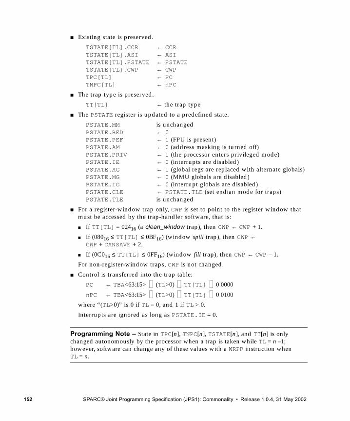
■ Existing state is preserved.
TSTATE[TL].CCR ← CCRTSTATE[TL].ASI ← ASITSTATE[TL].PSTATE ← PSTATETSTATE[TL].CWP ← CWPTPC[TL] ← PCTNPC[TL] ← nPC
■ The trap type is preserved.
TT[TL] ← the trap type
■ The PSTATE register is updated to a predefined state.
PSTATE.MM is unchangedPSTATE.RED ← 0PSTATE.PEF ← 1 (FPU is present)PSTATE.AM ← 0 (address masking is turned off)PSTATE.PRIV ← 1 (the processor enters privileged mode)PSTATE.IE ← 0 (interrupts are disabled)PSTATE.AG ← 1 (global regs are replaced with alternate globals)PSTATE.MG ← 0 (MMU globals are disabled)PSTATE.IG ← 0 (interrupt globals are disabled)PSTATE.CLE ← PSTATE.TLE (set endian mode for traps)PSTATE.TLE is unchanged
■ For a register-window trap only, CWP is set to point to the register window that must be accessed by the trap-handler software, that is:
■ If TT[TL] = 02416 (a clean_window trap), then CWP ← CWP + 1.
■ If (08016 ≤ TT[TL] ≤ 0BF16) (window spill trap), then CWP ←CWP + CANSAVE + 2.
■ If (0C016 ≤ TT[TL] ≤ 0FF16) (window fill trap), then CWP ← CWP – 1.
For non-register-window traps, CWP is not changed.
■ Control is transferred into the trap table:
PC ← TBA<63:15> (TL>0) TT[TL] 0 0000
nPC ← TBA<63:15> (TL>0) TT[TL] 0 0100
where “(TL>0)” is 0 if TL = 0, and 1 if TL > 0.
Interrupts are ignored as long as PSTATE.IE = 0.
Programming Note – State in TPC[n], TNPC[n], TSTATE[n], and TT[n] is only changed autonomously by the processor when a trap is taken while TL = n –1; however, software can change any of these values with a WRPR instruction when TL = n.
152 SPARC® Joint Programming Specification (JPS1): Commonality • Release 1.0.4, 31 May 2002
7.5.2 Fast MMU Trap ProcessingFast MMU traps (fast_instruction_access_MMU_miss, fast_data_access_MMU_miss, and fast_data_access_protection) cause the following state changes to occur:
■ If the processor is already in RED_state, the new trap is processed in RED_state unless TL = MAXTL. See Normal Traps When the Processor Is in RED_state on page 160.
■ If the processor is in execute_state and the trap level is one less than its maximum value, that is, TL = MAXTL–1, then the processor enters RED_state. See RED_state on page 133 and Normal Traps with TL = MAXTL – 1 on page 155.
■ If the processor is in either execute_state or RED_state and the trap level is already at its maximum value, that is, TL = MAXTL, then the processor enters error_state. See Error_state on page 136.
Otherwise, the trap uses normal trap processing, and the following state changes occur:
■ The trap level is set. This provides access to a fresh set of privileged trap-state registers used to save the current state, in effect, pushing a frame on the trap stack.
TL ← TL + 1
■ Existing state is preserved:
TSTATE[TL].CCR ← CCRTSTATE[TL].ASI ← ASITSTATE[TL].PSTATE ← PSTATETSTATE[TL].CWP ← CWPTPC[TL] ← PCTNPC[TL] ← nPC
■ The trap type is preserved.
TT[TL] ← the trap type
■ The PSTATE register is updated to a predefined state.
PSTATE.MM is unchangedPSTATE.RED ← 0PSTATE.PEF ← 1 (FPU is present)PSTATE.AM ← 0 (address masking is turned off)PSTATE.PRIV ← 1 (the processor enters privileged mode)PSTATE.IE ← 0 (interrupts are disabled)PSTATE.AG ← 0 (alternate globals are disabled)PSTATE.MG ← 1 (global regs are replaced with MMU globals)PSTATE.IG ← 0 (interrupt globals are disabled)PSTATE.CLE ← PSTATE.TLE (set endian mode for traps)PSTATE.TLE is unchanged
Release 1.0.4, 31 May 2002 C. Chapter 7 • Traps 153
■ For non-register-window traps, CWP is not changed.
■ Control is transferred into the trap table:
PC ← TBA<63:15> (TL>0) TT[TL] 0 0000
nPC ← TBA<63:15> (TL>0) TT[TL] 0 0100
where “(TL>0)” is 0 if TL = 0, and 1 if TL > 0.
Interrupts are ignored as long as PSTATE.IE = 0.
Programming Note – State in TPC[n], TNPC[n], TSTATE[n], and TT[n] is only changed autonomously by the processor when a trap is taken while TL = n – 1; however, software can change any of these values with a WRPR instruction when TL = n.
7.5.3 Interrupt Vector Trap Processing An interrupt_vector trap causes the following state changes to occur:
■ If the processor is already in RED_state, the new trap is processed in RED_state unless TL = MAXTL. See Normal Traps When the Processor Is in RED_state on page 160.
■ If the processor is in execute_state and the trap level is one less than its maximum value, that is, TL = MAXTL – 1, the processor enters RED_state. See RED_state on page 133 and Normal Traps with TL = MAXTL – 1 on page 155.
■ If the processor is in either execute_state or RED_state and the trap level is already at its maximum value, that is, TL = MAXTL, then the processor enters error_state. See Error_state on page 136.
Otherwise, the trap uses normal trap processing, and the following state changes occur:
■ The trap level is set. This provides access to a fresh set of privileged trap-state registers used to save the current state, in effect, pushing a frame on the trap stack.
TL ← TL + 1
■ Existing state is preserved.
TSTATE[TL].CCR ← CCRTSTATE[TL].ASI ← ASITSTATE[TL].PSTATE ← PSTATETSTATE[TL].CWP ← CWPTPC[TL] ← PCTNPC[TL] ← nPC
■ The trap type is preserved.
TT[TL] ← the trap type
154 SPARC® Joint Programming Specification (JPS1): Commonality • Release 1.0.4, 31 May 2002
■ The PSTATE register is updated to a predefined state.
PSTATE.MM is unchangedPSTATE.RED ← 0PSTATE.PEF ← 1 (FPU is present)PSTATE.AM ← 0 (address masking is turned off)PSTATE.PRIV ← 1 (the processor enters privileged mode)PSTATE.IE ← 0 (interrupts are disabled)PSTATE.AG ← 0 (alternate globals are disabled)PSTATE.MG ← 0 (MMU globals are disabled)PSTATE.IG ← 1 (global regs are replaced with interrupt globals)PSTATE.CLE ← PSTATE.TLE (set endian mode for traps)PSTATE.TLE is unchanged
■ For non-register-window traps, CWP is not changed.
■ Control is transferred into the trap table:
PC ← TBA<63:15> (TL>0) TT[TL] 0 0000
nPC ← TBA<63:15> (TL>0) TT[TL] 0 0100
where “(TL>0)” is 0 if TL = 0, and 1 if TL > 0.
Interrupts are ignored as long as PSTATE.IE = 0.
Programming Note – State in TPC[n], TNPC[n], TSTATE[n], and TT[n] is only changed autonomously by the processor when a trap is taken while TL = n – 1; however, software can change any of these values with a WRPR instruction when TL = n.
7.5.4 Special Trap ProcessingThe following conditions invoke special trap processing:
■ Traps taken with TL = MAXTL – 1■ Power-on reset traps■ Watchdog reset traps■ Externally initiated reset traps■ Software-initiated reset traps■ Traps taken when the processor is already in RED_state
IMPL. DEP. #38: Implementation-dependent registers may or may not be affected by the various reset traps.
Normal Traps with TL = MAXTL – 1
Normal traps that occur when TL = MAXTL – 1 are processed in RED_state. The following state changes occur:
Release 1.0.4, 31 May 2002 C. Chapter 7 • Traps 155
■ The trap level is advanced.
TL ← MAXTL
■ Existing state is preserved.
TSTATE[TL].CCR ← CCRTSTATE[TL].ASI ← ASITSTATE[TL].PSTATE ← PSTATETSTATE[TL].CWP ← CWPTPC[TL] ← PCTNPC[TL] ← nPC
■ The trap type is preserved.
TT[TL] ← the trap type
■ The PSTATE register is set as follows:
PSTATE.MM ← 002 (TSO)PSTATE.RED ← 1 (enter RED_state)PSTATE.PEF ← 1 (FPU is present)PSTATE.AM ← 0 (address masking is turned off)PSTATE.PRIV ← 1 (the processor enters privileged mode)PSTATE.IE ← 0 (interrupts are disabled)PSTATE.AG ← 1 (global regs are replaced with alternate globals)PSTATE.MG ← 0 (MMU globals are disabled)PSTATE.IG ← 0 (interrupt globals are disabled)PSTATE.CLE ← PSTATE.TLE (set endian mode for traps)PSTATE.TLE ← undefined1
■ For a register-window trap only, CWP is set to point to the register window that must be accessed by the trap-handler software, that is:
If TT[TL] = 02416 (a clean_window trap), then CWP ← CWP + 1.
If (08016 ≤ TT[TL] ≤ 0BF16) (window spill trap), then CWP ←CWP + CANSAVE + 2.
If (0C016 ≤ TT[TL] ≤ 0FF16) (window fill trap), then CWP ← CWP – 1.
For non-register-window traps, CWP is not changed.
■ Implementation-specific state changes; for example, disabling an MMU.
■ Control is transferred into the RED_state trap table.
PC ← RSTVaddr<63:8> 1010 00002
nPC ← RSTVaddr<63:8> 1010 01002
1. Note that this differs from SPARC V9.
156 SPARC® Joint Programming Specification (JPS1): Commonality • Release 1.0.4, 31 May 2002
Power-On Reset (POR) Traps
POR traps occur when power is applied to the processor. If the processor is in error_state, a POR brings the processor out of error_state and places it in RED_state. Processor state is undefined after POR, except for the following:
■ The trap level is set.
TL ← MAXTL
■ The trap type is set.
TT[TL] ← 00116
■ The PSTATE register is set as follows:
PSTATE.MM ← 002 (TSO)PSTATE.RED ← 1 (enter RED_state)PSTATE.PEF ← 1 (FPU is present)PSTATE.AM ← 0 (address masking is turned off)PSTATE.PRIV ← 1 (the processor enters privileged mode)PSTATE.IE ← 0 (interrupts are disabled)PSTATE.AG ← 1 (global regs are replaced with alternate globals)PSTATE.MG ← 0 (MMU globals are disabled)PSTATE.IG ← 0 (interrupt globals are disabled)PSTATE.CLE ← 0 (big-endian mode for nontraps)PSTATE.TLE ← 0 (big-endian mode for traps)
■ The TICK register is protected.
TICK.NPT ← 1 (TICK unreadable by nonprivileged software)
■ Implementation-specific state changes; for example, disabling an MMU.
■ Control is transferred into the RED_state trap table.
PC ← RSTVaddr<63:8> 0010 00002
nPC ← RSTVaddr<63:8> 0010 01002
For any reset when TL = MAXTL, for all n<MAXTL, the values in TPC[n], TNPC[n], and TSTATE[n] are undefined.
See SPARC JPS1 Implementation Supplements for more details.
Watchdog Reset (WDR) Traps
The WDR reset in SPARC JPS1 occurs when a watchdog timer overflows or to provide automatic recovery from error_state (impl. dep. #254). There are several causes of error_state entry (impl. dep. #39), including but not limited to SIR with TL = MAXTL and implementation-dependent watchdog timeout.
Processor state is undefined after WDR, except for the following:
■ The trap level is set.
Release 1.0.4, 31 May 2002 C. Chapter 7 • Traps 157
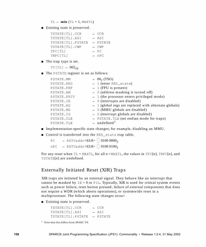
TL ← min (TL + 1, MAXTL)
■ Existing state is preserved.
TSTATE[TL].CCR ← CCRTSTATE[TL].ASI ← ASITSTATE[TL].PSTATE ← PSTATETSTATE[TL].CWP ← CWPTPC[TL] ← PCTNPC[TL] ← nPC
■ The trap type is set.
TT[TL] ← 00216
■ The PSTATE register is set as follows:
PSTATE.MM ← 002 (TSO)PSTATE.RED ← 1 (enter RED_state)PSTATE.PEF ← 1 (FPU is present)PSTATE.AM ← 0 (address masking is turned off)PSTATE.PRIV ← 1 (the processor enters privileged mode)PSTATE.IE ← 0 (interrupts are disabled)PSTATE.AG ← 1 (global regs are replaced with alternate globals)PSTATE.MG ← 0 (MMU globals are disabled)PSTATE.IG ← 0 (interrupt globals are disabled)PSTATE.CLE ← PSTATE.TLE (set endian mode for traps)PSTATE.TLE ← undefined1
■ Implementation-specific state changes; for example, disabling an MMU.
■ Control is transferred into the RED_state trap table.
PC ← RSTVaddr<63:8> 0100 00002
nPC ← RSTVaddr<63:8> 0100 01002
For any reset when TL = MAXTL, for all n<MAXTL, the values in TPC[n], TNPC[n], and TSTATE[n] are undefined.
Externally Initiated Reset (XIR) Traps
XIR traps are initiated by an external signal. They behave like an interrupt that cannot be masked by IE = 0 or PIL. Typically, XIR is used for critical system events such as power failure, reset button pressed, failure of external components that does not require a WDR (which aborts operations), or systemwide reset in a multiprocessor. The following state changes occur:
■ Existing state is preserved.
TSTATE[TL].CCR ← CCRTSTATE[TL].ASI ← ASITSTATE[TL].PSTATE ← PSTATE
1. Note that this differs from SPARC V9.
158 SPARC® Joint Programming Specification (JPS1): Commonality • Release 1.0.4, 31 May 2002
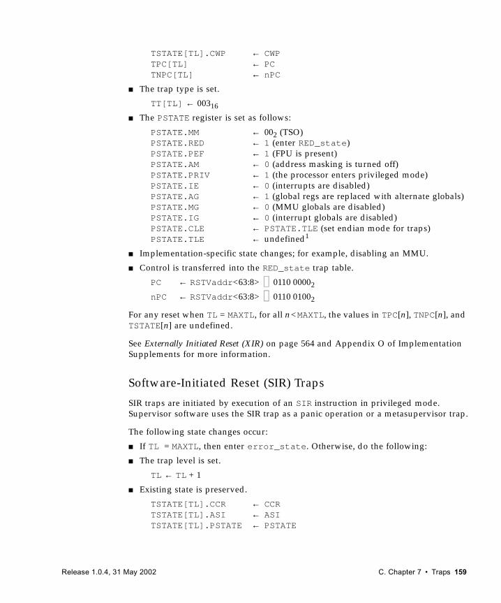
TSTATE[TL].CWP ← CWPTPC[TL] ← PCTNPC[TL] ← nPC
■ The trap type is set.
TT[TL] ← 00316
■ The PSTATE register is set as follows:
PSTATE.MM ← 002 (TSO)PSTATE.RED ← 1 (enter RED_state)PSTATE.PEF ← 1 (FPU is present)PSTATE.AM ← 0 (address masking is turned off)PSTATE.PRIV ← 1 (the processor enters privileged mode)PSTATE.IE ← 0 (interrupts are disabled)PSTATE.AG ← 1 (global regs are replaced with alternate globals)PSTATE.MG ← 0 (MMU globals are disabled)PSTATE.IG ← 0 (interrupt globals are disabled)PSTATE.CLE ← PSTATE.TLE (set endian mode for traps)PSTATE.TLE ← undefined1
■ Implementation-specific state changes; for example, disabling an MMU.
■ Control is transferred into the RED_state trap table.
PC ← RSTVaddr<63:8> 0110 00002
nPC ← RSTVaddr<63:8> 0110 01002
For any reset when TL = MAXTL, for all n<MAXTL, the values in TPC[n], TNPC[n], and TSTATE[n] are undefined.
See Externally Initiated Reset (XIR) on page 564 and Appendix O of Implementation Supplements for more information.
Software-Initiated Reset (SIR) Traps
SIR traps are initiated by execution of an SIR instruction in privileged mode. Supervisor software uses the SIR trap as a panic operation or a metasupervisor trap.
The following state changes occur:
■ If TL = MAXTL, then enter error_state. Otherwise, do the following:
■ The trap level is set.
TL ← TL + 1
■ Existing state is preserved.
TSTATE[TL].CCR ← CCRTSTATE[TL].ASI ← ASITSTATE[TL].PSTATE ← PSTATE
Release 1.0.4, 31 May 2002 C. Chapter 7 • Traps 159
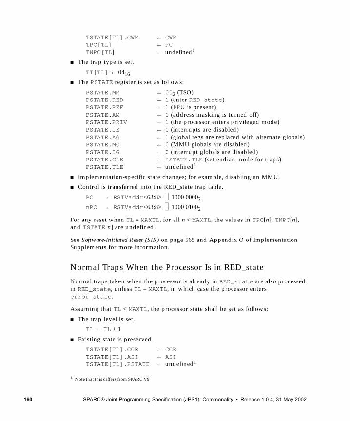
TSTATE[TL].CWP ← CWPTPC[TL] ← PCTNPC[TL] ← undefined1
■ The trap type is set.
TT[TL] ← 0416
■ The PSTATE register is set as follows:
PSTATE.MM ← 002 (TSO)PSTATE.RED ← 1 (enter RED_state)PSTATE.PEF ← 1 (FPU is present)PSTATE.AM ← 0 (address masking is turned off)PSTATE.PRIV ← 1 (the processor enters privileged mode)PSTATE.IE ← 0 (interrupts are disabled)PSTATE.AG ← 1 (global regs are replaced with alternate globals)PSTATE.MG ← 0 (MMU globals are disabled)PSTATE.IG ← 0 (interrupt globals are disabled)PSTATE.CLE ← PSTATE.TLE (set endian mode for traps)PSTATE.TLE ← undefined1
■ Implementation-specific state changes; for example, disabling an MMU.
■ Control is transferred into the RED_state trap table.
PC ← RSTVaddr<63:8> 1000 00002
nPC ← RSTVaddr<63:8> 1000 01002
For any reset when TL = MAXTL, for all n < MAXTL, the values in TPC[n], TNPC[n], and TSTATE[n] are undefined.
See Software-Initiated Reset (SIR) on page 565 and Appendix O of Implementation Supplements for more information.
Normal Traps When the Processor Is in RED_state
Normal traps taken when the processor is already in RED_state are also processed in RED_state, unless TL = MAXTL, in which case the processor enters error_state.
Assuming that TL < MAXTL, the processor state shall be set as follows:
■ The trap level is set.
TL ← TL + 1
■ Existing state is preserved.
TSTATE[TL].CCR ← CCRTSTATE[TL].ASI ← ASITSTATE[TL].PSTATE ← undefined1
1. Note that this differs from SPARC V9.
160 SPARC® Joint Programming Specification (JPS1): Commonality • Release 1.0.4, 31 May 2002
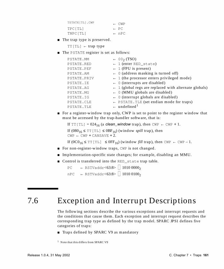
TSTATE[TL].CWP ← CWPTPC[TL] ← PCTNPC[TL] ← nPC
■ The trap type is preserved.
TT[TL] ← trap type
■ The PSTATE register is set as follows:
PSTATE.MM ← 002 (TSO)PSTATE.RED ← 1 (enter RED_state)PSTATE.PEF ← 1 (FPU is present)PSTATE.AM ← 0 (address masking is turned off)PSTATE.PRIV ← 1 (the processor enters privileged mode)PSTATE.IE ← 0 (interrupts are disabled)PSTATE.AG ← 1 (global regs are replaced with alternate globals)PSTATE.MG ← 0 (MMU globals are disabled)PSTATE.IG ← 0 (interrupt globals are disabled)PSTATE.CLE ← PSTATE.TLE (set endian mode for traps)PSTATE.TLE ← undefined1
■ For a register-window trap only, CWP is set to point to the register window that must be accessed by the trap-handler software, that is:
If TT[TL] = 02416 (a clean_window trap), then CWP ← CWP + 1.
If (08016 ≤ TT[TL] ≤ 0BF16) (window spill trap), thenCWP ← CWP + CANSAVE + 2.
If (0C016 ≤ TT[TL] ≤ 0FF16) (window fill trap), then CWP ← CWP – 1.
■ For non-register-window traps, CWP is not changed.
■ Implementation-specific state changes; for example, disabling an MMU.
■ Control is transferred into the RED_state trap table.
PC ← RSTVaddr<63:8> 1010 00002
nPC ← RSTVaddr<63:8> 1010 01002
7.6 Exception and Interrupt DescriptionsThe following sections describe the various exceptions and interrupt requests and the conditions that cause them. Each exception and interrupt request describes the corresponding trap type as defined by the trap model. SPARC JPS1 defines five categories of traps:
■ Traps defined by SPARC V9 as mandatory
1. Note that this differs from SPARC V9
Release 1.0.4, 31 May 2002 C. Chapter 7 • Traps 161
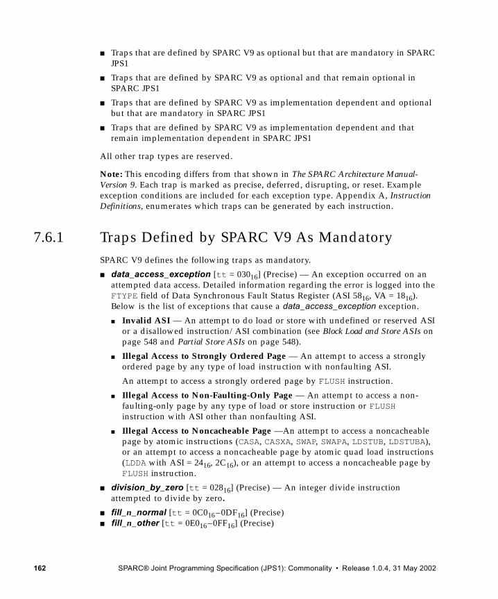
■ Traps that are defined by SPARC V9 as optional but that are mandatory in SPARC JPS1
■ Traps that are defined by SPARC V9 as optional and that remain optional in SPARC JPS1
■ Traps that are defined by SPARC V9 as implementation dependent and optional but that are mandatory in SPARC JPS1
■ Traps that are defined by SPARC V9 as implementation dependent and that remain implementation dependent in SPARC JPS1
All other trap types are reserved.
Note: This encoding differs from that shown in The SPARC Architecture Manual-Version 9. Each trap is marked as precise, deferred, disrupting, or reset. Example exception conditions are included for each exception type. Appendix A, Instruction Definitions, enumerates which traps can be generated by each instruction.
7.6.1 Traps Defined by SPARC V9 As MandatorySPARC V9 defines the following traps as mandatory.
■ data_access_exception [tt = 03016] (Precise) — An exception occurred on an attempted data access. Detailed information regarding the error is logged into the FTYPE field of Data Synchronous Fault Status Register (ASI 5816, VA = 1816). Below is the list of exceptions that cause a data_access_exception exception.
■ Invalid ASI — An attempt to do load or store with undefined or reserved ASI or a disallowed instruction/ASI combination (see Block Load and Store ASIs on page 548 and Partial Store ASIs on page 548).
■ Illegal Access to Strongly Ordered Page — An attempt to access a strongly ordered page by any type of load instruction with nonfaulting ASI.
An attempt to access a strongly ordered page by FLUSH instruction.
■ Illegal Access to Non-Faulting-Only Page — An attempt to access a non-faulting-only page by any type of load or store instruction or FLUSH instruction with ASI other than nonfaulting ASI.
■ Illegal Access to Noncacheable Page —An attempt to access a noncacheable page by atomic instructions (CASA, CASXA, SWAP, SWAPA, LDSTUB, LDSTUBA), or an attempt to access a noncacheable page by atomic quad load instructions (LDDA with ASI = 2416, 2C16), or an attempt to access a noncacheable page by FLUSH instruction.
■ division_by_zero [tt = 02816] (Precise) — An integer divide instruction attempted to divide by zero.
■ fill_n_normal [tt = 0C016–0DF16] (Precise)■ fill_n_other [tt = 0E016–0FF16] (Precise)
162 SPARC® Joint Programming Specification (JPS1): Commonality • Release 1.0.4, 31 May 2002
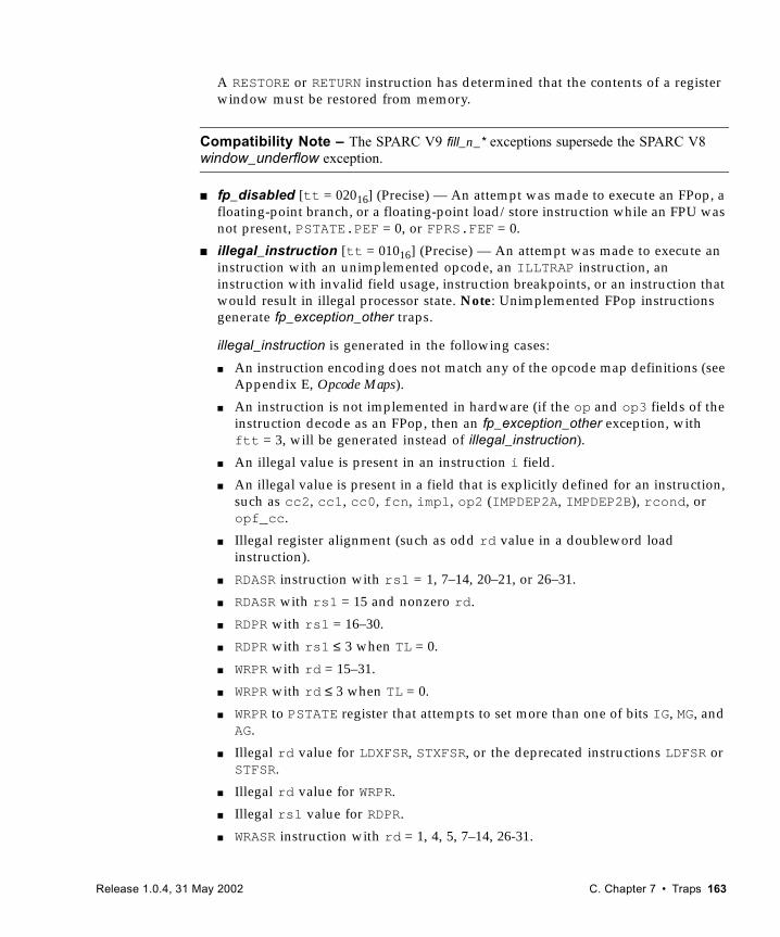
A RESTORE or RETURN instruction has determined that the contents of a register window must be restored from memory.
Compatibility Note – The SPARC V9 fill_n_* exceptions supersede the SPARC V8 window_underflow exception.
■ fp_disabled [tt = 02016] (Precise) — An attempt was made to execute an FPop, a floating-point branch, or a floating-point load/store instruction while an FPU was not present, PSTATE.PEF = 0, or FPRS.FEF = 0.
■ illegal_instruction [tt = 01016] (Precise) — An attempt was made to execute an instruction with an unimplemented opcode, an ILLTRAP instruction, an instruction with invalid field usage, instruction breakpoints, or an instruction that would result in illegal processor state. Note: Unimplemented FPop instructions generate fp_exception_other traps.
illegal_instruction is generated in the following cases:
■ An instruction encoding does not match any of the opcode map definitions (see Appendix E, Opcode Maps).
■ An instruction is not implemented in hardware (if the op and op3 fields of the instruction decode as an FPop, then an fp_exception_other exception, with ftt = 3, will be generated instead of illegal_instruction).
■ An illegal value is present in an instruction i field.
■ An illegal value is present in a field that is explicitly defined for an instruction, such as cc2, cc1, cc0, fcn, impl, op2 (IMPDEP2A, IMPDEP2B), rcond, or opf_cc.
■ Illegal register alignment (such as odd rd value in a doubleword load instruction).
■ RDASR instruction with rs1 = 1, 7–14, 20–21, or 26–31.
■ RDASR with rs1 = 15 and nonzero rd.
■ RDPR with rs1 = 16–30.
■ RDPR with rs1 ≤ 3 when TL = 0.
■ WRPR with rd = 15–31.
■ WRPR with rd ≤ 3 when TL = 0.
■ WRPR to PSTATE register that attempts to set more than one of bits IG, MG, and AG.
■ Illegal rd value for LDXFSR, STXFSR, or the deprecated instructions LDFSR or STFSR.
■ Illegal rd value for WRPR.
■ Illegal rs1 value for RDPR.
■ WRASR instruction with rd = 1, 4, 5, 7–14, 26-31.
Release 1.0.4, 31 May 2002 C. Chapter 7 • Traps 163
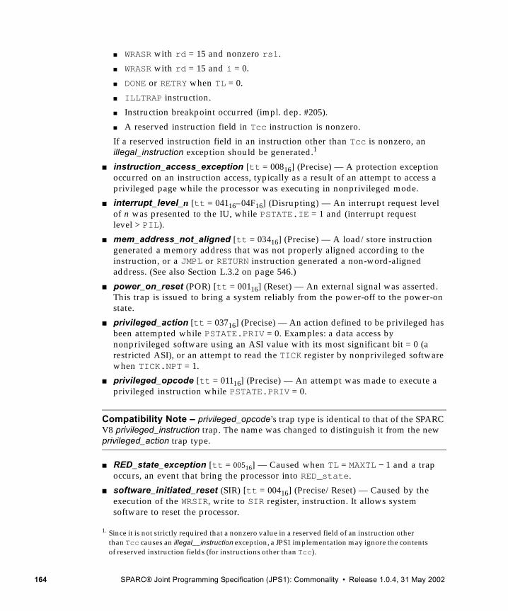
■ WRASR with rd = 15 and nonzero rs1.
■ WRASR with rd = 15 and i = 0.
■ DONE or RETRY when TL = 0.
■ ILLTRAP instruction.
■ Instruction breakpoint occurred (impl. dep. #205).
■ A reserved instruction field in Tcc instruction is nonzero.
If a reserved instruction field in an instruction other than Tcc is nonzero, an illegal_instruction exception should be generated.1
■ instruction_access_exception [tt = 00816] (Precise) — A protection exception occurred on an instruction access, typically as a result of an attempt to access a privileged page while the processor was executing in nonprivileged mode.
■ interrupt_level_n [tt = 04116–04F16] (Disrupting) — An interrupt request level of n was presented to the IU, while PSTATE.IE = 1 and (interrupt request level > PIL).
■ mem_address_not_aligned [tt = 03416] (Precise) — A load/store instruction generated a memory address that was not properly aligned according to the instruction, or a JMPL or RETURN instruction generated a non-word-aligned address. (See also Section L.3.2 on page 546.)
■ power_on_reset (POR) [tt = 00116] (Reset) — An external signal was asserted. This trap is issued to bring a system reliably from the power-off to the power-on state.
■ privileged_action [tt = 03716] (Precise) — An action defined to be privileged has been attempted while PSTATE.PRIV = 0. Examples: a data access by nonprivileged software using an ASI value with its most significant bit = 0 (a restricted ASI), or an attempt to read the TICK register by nonprivileged software when TICK.NPT = 1.
■ privileged_opcode [tt = 01116] (Precise) — An attempt was made to execute a privileged instruction while PSTATE.PRIV = 0.
Compatibility Note – privileged_opcode’s trap type is identical to that of the SPARC V8 privileged_instruction trap. The name was changed to distinguish it from the new privileged_action trap type.
■ RED_state_exception [tt = 00516] — Caused when TL = MAXTL − 1 and a trap occurs, an event that bring the processor into RED_state.
■ software_initiated_reset (SIR) [tt = 00416] (Precise/Reset) — Caused by the execution of the WRSIR, write to SIR register, instruction. It allows system software to reset the processor.
1. Since it is not strictly required that a nonzero value in a reserved field of an instruction other than Tcc causes an illegal__instruction exception, a JPS1 implementation may ignore the contents of reserved instruction fields (for instructions other than Tcc).
164 SPARC® Joint Programming Specification (JPS1): Commonality • Release 1.0.4, 31 May 2002
■ spill_n_normal [tt = 08016–09F16] (Precise)■ spill_n_other [tt = 0A016–0BF16] (Precise)
A SAVE or FLUSHW instruction has determined that the contents of a register window must be saved to memory.
Compatibility Note – The SPARC V9 spill_n_* exceptions supersede the SPARC V8 window_overflow exception.
■ tag_overflow [tt = 02316] (Precise) — A TADDccTV or TSUBccTV instruction was executed, and either 32-bit arithmetic overflow occurred or at least one of the tag bits of the operands was nonzero.
■ trap_instruction [tt = 10016–17F16] (Precise) — A Tcc instruction was executed and the trap condition evaluated to TRUE.
7.6.2 SPARC V9 Optional Traps That Are Mandatory in SPARC JPS1SPARC V9 defines the following traps as optional. However, the traps are mandatory in SPARC JPS1.
■ clean_window [tt = 02416–02716] (Precise) — A SAVE instruction discovered that the window about to be used contains data from another address space; the window must be cleaned before it can be used.
IMPL. DEP. #102: An implementation may choose either to implement automatic cleaning of register windows in hardware or to generate a clean_window trap, when needed, so that window(s) can be cleaned by software. If an implementation chooses the latter option, then support for this trap type is mandatory.
■ data_access_error [tt = 03216] (Precise or Deferred) — An error occurred on a data access.
■ externally_initiated_reset (XIR) [tt = 00316] (Reset) — An external signal was asserted. This trap is used for catastrophic events such as power failure, reset button pressed, and systemwide reset in multiprocessor systems.
■ fp_exception_ieee_754 [tt = 02116] (Precise) — An FPop instruction generated an IEEE_754_exception and its corresponding trap enable mask (TEM) bit was 1. The floating-point exception type, IEEE_754_exception, is encoded in the FSR.ftt, and specific IEEE_754_exception information is encoded in FSR.cexc.
■ fp_exception_other [tt = 02216] (Precise) — An FPop instruction generated an exception other than an IEEE_754_exception. Examples: the FPop is unimplemented, or there was a sequence or hardware error in the FPU. The floating-point exception type is encoded in the FSR’s ftt field.
Release 1.0.4, 31 May 2002 C. Chapter 7 • Traps 165
■ instruction_access_error [tt = 00A16] (Precise) — An error occurred on an instruction access.
■ LDDF_mem_address_not_aligned [tt = 03516] (Precise) — An attempt was made to execute an LDDF instruction and the effective address was not doubleword aligned. See Section A.26, Load Floating-Point and Section A.27, Load Floating-Point from Alternate Space.
■ STDF_mem_address_not_aligned [tt = 03616] (Precise) — An attempt was made to execute an STDF instruction and the effective address was not doubleword aligned. See A.61, Store Floating-Point on page 330.
■ watchdog reset (WDR) [tt = 00216] (Reset) — This trap occurs when the watchdog timer overflows or as a transition from error_state to RED_state (impl. dep. #254).
7.6.3 SPARC V9 Optional Traps That Are Optional in SPARC JPS1SPARC V9 defines the following traps as optional. The traps remain optional in SPARC JPS1.
■ data_access_MMU_miss [tt = 03116] (Precise or Deferred) (impl. dep. #) — This exception is generally superseded by fast_data_access_MMU_miss (see section 7.6.4).
■ data_access_protection [tt = 03316] (Precise or Deferred) (impl. dep. #) — This exception is generally superseded by fast_data_access_protection (see section 7.6.4).
■ LDQF_mem_address_not_aligned [tt = 03816] (Precise or Deferred) — An attempt was made to execute an LDQF instruction and the effective address was word aligned but not quadword aligned. Use of this exception is implementation dependent (impl. dep. #111). A separate trap entry for this exception supports fast software emulation of the LDQF instruction when the effective address is word aligned but not quadword aligned. See A.26, Load Floating-Point on page 242.
■ STQF_mem_address_not_aligned [tt = 03916] (Precise) — An attempt was made to execute an STQF instruction and the effective address was word aligned but not quadword aligned. Use of this exception is implementation dependent (impl. dep. #112). A separate trap entry for the exception supports fast software emulation of the STQF instruction when the effective address is word aligned but not quadword aligned. See A.61, Store Floating-Point on page 330.
■ instruction_access_MMU_miss [tt = 00916] (Precise, Deferred, or Disrupting) (impl. dep. #) — This exception is generally superseded by fast_instruction_access_MMU_miss (see section 7.6.4).
■ unimplemented_LDD [tt = 01216] (Precise) — An attempt was made to execute an LDD instruction, which is not implemented in hardware on this implementation (impl. dep. #107).
166 SPARC® Joint Programming Specification (JPS1): Commonality • Release 1.0.4, 31 May 2002
■ unimplemented_STD [tt = 01316] (Precise) — An attempt was made to execute an STD instruction, which is not implemented in hardware on this implementation (impl. dep. #108).
7.6.4 SPARC V9 Implementation-Dependent, Optional Traps That Are Mandatory in SPARC JPS1SPARC V9 defines the following traps as implementation dependent and optional. The traps are mandatory in SPARC JPS1.
■ ECC_error [tt = 06316] (Disrupting) — The trap to signal the detection of hardware errors asynchronous to the instruction execution, or to request to save the information logged for the error that was detected and corrected by the processor.
Implementation Note – Some implementations may refer to this trap by the name “corrected_ECC_error.”
■ fast_data_access_MMU_miss [tt = 06816 –06B16] (Precise) — During an attempted data access, the MMU detected that a translation lookaside buffer did not contain a translation for the virtual address (that is, a TLB miss occurred). Four trap vectors are allocated for this trap, allowing a TLB miss handler of up to 32 instructions to fit within the trap vector area.
■ fast_data_access_protection [tt = 06C16–06F16] (Precise) — During an attempted data write access (by a store or load-store instruction), the instruction had appropriate access privilege but the MMU signalled that the location was write-protected (write to a read-only location). Note that on a JPS1 processor, an attempt to read or write to a privileged location while in nonprivileged mode causes the higher-priority data_access_exception instead of this exception. Four trap vectors are allocated for this trap, allowing a trap handler of up to 32 instructions to fit within the trap vector area.
■ fast_instruction_access_MMU_miss [tt = 06416 –06716] (Precise) — During an attempted instruction access, the MMU detected a TLB miss. Four trap vectors are allocated for this trap, allowing a trap handler of up to 32 instructions to fit within the trap vector area.
■ interrupt_vector_trap [tt = 06016] (Disrupting) — The processor has received an interrupt request.
■ PA_watchpoint [tt = 06116] (Precise) — The processor has detected a physical-address breakpoint.
■ VA_watchpoint [tt = 06216] (Precise) — The processor has detected a virtual-address breakpoint.
Release 1.0.4, 31 May 2002 C. Chapter 7 • Traps 167
7.6.5 SPARC JPS1 Implementation-Dependent TrapsThe following traps are implementation dependent in SPARC JPS1.
■ async_data_error [tt = 04016] (Precise, Deferred, or Disrupting) — An implementation-dependent exception (impl. dep. #31, #218) that indicates that one or more unrecoverable or uncorrectable but recoverable errors have been detected in the processor. This may include errors detected in the architectural registers (general-purpose registers, floating-point registers, ASRs, or ASI registers) and other core processor hardware. A single async_data_error exception may indicate multiple errors and may occur asynchronously to instruction execution. An async_data_error exception may cause a precise, deferred, or disrupting trap. When async_data_error causes a disrupting trap, the TPC and TNPC stacked by the trap do not necessarily indicate the instruction or data access that caused the error.
Compatibility Note – The SPARC V9 async_data_error supersedes the less general SPARC V8 data_store_error exception.
IMPL. DEP. #218: Whether async_data_error exception is implemented is implementation dependent. If it does exist, it indicates that an error is detected in a processor core and its trap type is 4016. The SPARC V9 async_data_error supersedes the less general SPARC V8 data_store_error exception.
■ fast_ECC_error [tt = 07016] (Precise) — A single-bit or multiple-bit ECC error is detected.
IMPL. DEP. #: Whether or not a fast_ECC_error trap exists is implementation dependent. If it does exist, it indicates that an ECC error was detected in an external cache and its trap type is 07016.
■ internal_processor_error [tt = 02916] (Precise, Deferred, or Disrupting) — A serious internal error occurred in the main processor (impl. dep. #).
168 SPARC® Joint Programming Specification (JPS1): Commonality • Release 1.0.4, 31 May 2002
C.CHAPTER 8
Memory Models
The SPARC V9 memory models define the semantics of memory operations. The instruction set semantics require that loads and stores seem to be performed in the order in which they appear in the dynamic control flow of the program. The actual order in which they are processed by the memory may be different. The purpose of the memory models is to specify what constraints, if any, are placed on the order of memory operations.
The memory models apply both to uniprocessor and to shared memory multiprocessors. Formal memory models are necessary for precise definitions of the interactions between multiple processors and input/output devices in a shared memory configuration. Programming shared memory multiprocessors requires a detailed understanding of the operative memory model and the ability to specify memory operations at a low level in order to build programs that can safely and reliably coordinate their activities. See Appendix J, Programming with the Memory Models, for additional information on the use of the models in programming real systems.
Although this chapter contains a great deal of theoretical information, we have included that information so the discussion of the implementation-specific memory models has sufficient background.
We describe memory models in these sections:
■ Overview on page 170■ Memory, Real Memory, and I/O Locations on page 171■ Addressing and Alternate Address Spaces on page 173■ SPARC V9 Memory Model on page 175
Release 1.0.4, 31 May 2002 C. Chapter 8 • Memory Models 169
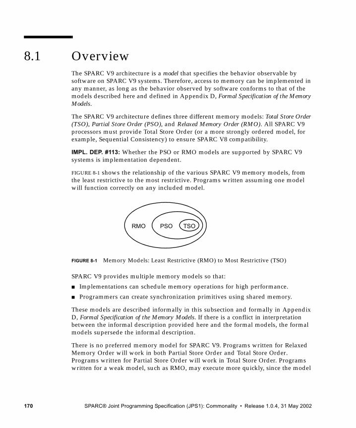
8.1 OverviewThe SPARC V9 architecture is a model that specifies the behavior observable by software on SPARC V9 systems. Therefore, access to memory can be implemented in any manner, as long as the behavior observed by software conforms to that of the models described here and defined in Appendix D, Formal Specification of the Memory Models.
The SPARC V9 architecture defines three different memory models: Total Store Order (TSO), Partial Store Order (PSO), and Relaxed Memory Order (RMO). All SPARC V9 processors must provide Total Store Order (or a more strongly ordered model, for example, Sequential Consistency) to ensure SPARC V8 compatibility.
IMPL. DEP. #113: Whether the PSO or RMO models are supported by SPARC V9 systems is implementation dependent.
FIGURE 8-1 shows the relationship of the various SPARC V9 memory models, from the least restrictive to the most restrictive. Programs written assuming one model will function correctly on any included model.
FIGURE 8-1 Memory Models: Least Restrictive (RMO) to Most Restrictive (TSO)
SPARC V9 provides multiple memory models so that:
■ Implementations can schedule memory operations for high performance.
■ Programmers can create synchronization primitives using shared memory.
These models are described informally in this subsection and formally in Appendix D, Formal Specification of the Memory Models. If there is a conflict in interpretation between the informal description provided here and the formal models, the formal models supersede the informal description.
There is no preferred memory model for SPARC V9. Programs written for Relaxed Memory Order will work in both Partial Store Order and Total Store Order. Programs written for Partial Store Order will work in Total Store Order. Programs written for a weak model, such as RMO, may execute more quickly, since the model
RMO PSO TSO
170 SPARC® Joint Programming Specification (JPS1): Commonality • Release 1.0.4, 31 May 2002
exposes more scheduling opportunities, but may also require extra instructions to ensure synchronization. Multiprocessor programs written for a stronger model will behave unpredictably if run in a weaker model.
Machines that implement sequential consistency (also called strong ordering or strong consistency) automatically support programs written for TSO, PSO, and RMO. Sequential consistency is not a SPARC V9 memory model. In sequential consistency, the loads, stores, and atomic load-stores of all processors are performed by memory in a serial order that conforms to the order in which these instructions are issued by individual processors. A machine that implements sequential consistency may deliver lower performance than an equivalent machine that implements a weaker model. Although particular SPARC V9 implementations may support sequential consistency, portable software must not rely on having this model available.
Notes About the Implementation of the Memory Models
From the programmer’s point of view, a SPARC V9 implementation completely supports the memory models specified in SPARC V9.
SPARC V9 does not specify exactly how the hardware must support a particular SPARC V9 memory model, except that the hardware support for the V9 memory model must guarantee that a correct program written for that memory model will run correctly on the hardware. For example, a slightly stronger (more restrictive) hardware memory model might be used than that required by the SPARC V9 memory model.
8.2 Memory, Real Memory, and I/O LocationsMemory is the collection of locations accessed by the load and store instructions (described in Appendix A, Instruction Definitions). Each location is identified by an address consisting of two elements: an address space identifier (ASI), which identifies an address space, and a 64-bit address, which is a byte offset into that address space. Memory addresses may be interpreted by the memory subsystem to be either physical addresses or virtual addresses; addresses may be remapped and values cached, provided that memory properties are preserved transparently and coherency is maintained.
When two or more data addresses refer to the same datum, the address is said to be aliased. In this case, the processor and memory system must cooperate to maintain consistency; that is, a store to an aliased address must change all values aliased to that address.
Release 1.0.4, 31 May 2002 C. Chapter 8 • Memory Models 171
Memory addresses identify either real memory or I/O locations.
Real memory stores information without side effects. A load operation returns the value most recently stored. Operations are side-effect-free in the sense that a load, store, or atomic load-store to a location in real memory has no program-observable effect, except upon that location.
I/O locations may not behave like memory and may have side effects. Load, store, and atomic load-store operations performed on I/O locations may have observable side effects, and loads may not return the value most recently stored. The value semantics of operations on I/O locations are not defined by the memory models, but the constraints on the order in which operations are performed is the same as it would be if the I/O locations were real memory. The storage properties, contents, semantics, ASI assignments, and addresses of I/O registers are implementation dependent.
IMPL. DEP. #118: The manner in which I/O locations are identified is implementation dependent.
IMPL. DEP. #120: The coherence and atomicity of memory operations between processors and I/O DMA memory accesses are implementation dependent.
Implementation Note – Operations to I/O locations are not guaranteed to be sequentially consistent among themselves, as they are in SPARC V8.
SPARC V9 does not distinguish real memory from I/O locations in terms of ordering. All references, both to I/O locations and real memory, conform to the memory model’s order constraints. References to I/O locations may need to be interspersed with MEMBAR instructions to guarantee the desired ordering.
Systems supporting SPARC V8 applications that use memory mapped I/O locations must ensure that SPARC V8 sequential consistency of I/O locations can be maintained when those locations are referenced by a SPARC V8 application. The MMU either must enforce such consistency or cooperate with system software or the processor to provide it.
IMPL. DEP. #121: An implementation may choose to identify certain addresses and use an implementation-dependent memory model for references to them.
172 SPARC® Joint Programming Specification (JPS1): Commonality • Release 1.0.4, 31 May 2002
8.3 Addressing and Alternate Address SpacesAn address in SPARC V9 is a tuple consisting of an 8-bit address space identifier (ASI) and a 64-bit byte-address offset in the specified address space. Memory is byte-addressed, with halfword accesses aligned on 2-byte boundaries, word accesses (which include instruction fetches) aligned on 4-byte boundaries, extended-word and doubleword accesses aligned on 8-byte boundaries, and quadword quantities aligned on 16-byte boundaries. With the possible exception of the cases described in Memory Alignment Restrictions on page 108, an improperly aligned address in a load, store, or load-store instruction always causes a trap to occur. The largest datum that is guaranteed to be atomically read or written is an aligned doubleword.1 Also, memory references to different bytes, halfwords, and words in a given doubleword are treated for ordering purposes as references to the same location. Thus, the unit of ordering for memory is a doubleword.
Notes – The doubleword is the coherency unit for update, but programmers should not assume that doubleword floating-point values are updated as a unit unless they are doubleword-aligned and always updated with double-precision loads and stores. Some programs use pairs of single-precision operations to load and store double-precision floating-point values when the compiler cannot determine that they are doubleword aligned.
Also, although quad-precision operations are defined in the SPARC V9 architecture, the granularity of loads and stores for quad-precision floating-point values may be word or doubleword.
The processor provides an address space identifier with every address. This ASI may serve several purposes:
■ To identify which of several distinguished address spaces the 64-bit address offset is addressing
■ To provide additional access control and attribute information, for example, to identify the processing that is to be performed if an access fault occurs, or to specify the endianness of the reference
■ To specify the address of an internal control register in the processor, cache, or memory management hardware
1. Two exceptions to this are the special ASI_NUCLEUS_QUAD_LDD[_L] and ASI_QUAD_LDD_PHYS[_L] which provide hardware support for an atomic quad load to be used for TTE loads from TSBs.
Release 1.0.4, 31 May 2002 C. Chapter 8 • Memory Models 173
The memory management hardware can associate an independent 264-byte memory address space with each ASI. If this is done, it becomes possible to allow system software easy access to the address space of the faulting program when processing exceptions or to implement access to a client program’s memory space by a server program.
The architecturally specified ASIs are listed in Appendix L, Address Space Identifiers.
When TL = 0, normal accesses by the processor to memory when fetching instructions and performing loads and stores implicitly specify ASI_PRIMARY or ASI_PRIMARY_LITTLE, depending on the setting of the PSTATE.CLE bit.
When TL > 0, the implicit ASI for instruction fetches is ASI_NUCLEUS; loads and stores will use ASI_NUCLEUS if PSTATE.CLE = 0 or ASI_NUCLEUS_LITTLE if PSTATE.CLE = 1 (impl. dep. #124).
SPARC V9 supports the PRIMARY{_LITTLE}, SECONDARY{_LITTLE}, and NUCLEUS{_LITTLE} address spaces.
Accesses to other address spaces use the load/store alternate instructions. For these accesses, the ASI is either contained in the instruction (for the register-register addressing mode) or taken from the ASI register (for register-immediate addressing).
ASIs are either nonrestricted or restricted. A nonrestricted ASI is one that may be used independently of the privilege level (PSTATE.PRIV) at which the processor is running. Restricted ASIs require that the processor be in privileged mode for a legal access to occur. Restricted ASIs have their high-order bit equal to 0. The relationship between processor state and ASI restriction is shown in TABLE 6-2 on page 112.
Several restricted ASIs are provided as mandated by SPARC V9: ASI_AS_IF_USER_PRIMARY{_LITTLE} and ASI_AS_IF_USER_SECONDARY{_LITTLE}. The intent of these ASIs is to give system software efficient access to the memory space of a program.
The normal address space is primary address space, which is accessed by the unrestricted ASI_PRIMARY{_LITTLE}. The secondary address space, which is accessed by the unrestricted ASI_SECONDARY{_LITTLE}, is provided to allow a server program to access a client program’s address space.
ASI_PRIMARY_NOFAULT{_LITTLE} and ASI_SECONDARY_NOFAULT{_LITTLE} support nonfaulting loads. These ASIs are aliased to ASI_PRIMARY{_LITTLE} and ASI_SECONDARY{_LITTLE}, respectively, and have exactly the same action. They may be used to color (that is, distinguish into classes) loads in the instruction stream so that, in combination with a judicious mapping of low memory and a specialized trap handler, an optimizing compiler can move loads outside of conditional control structures.
174 SPARC® Joint Programming Specification (JPS1): Commonality • Release 1.0.4, 31 May 2002

Notes – Nonfaulting loads allow optimizations that move loads ahead of conditional control structures that guard their use; thus, they can minimize the effects of load latency by improving instruction scheduling. The semantics of nonfaulting loads are the same as for any other load, except when nonrecoverable catastrophic faults occur (for example, a reference to a nonexisting or invalid page). When such a fault occurs, it is ignored and the hardware and system software cooperate to make the load appear to complete normally, returning a zero result. The compiler’s optimizer generates load-alternate instructions with the ASI field or register set to ASI_PRIMARY_NOFAULT{_LITTLE} or ASI_SECONDARY_NOFAULT{_LITTLE} for those loads it determines should be nonfaulting.
To minimize unnecessary processing if a fault does occur, map low addresses (especially address zero) to a page of all zeroes, so that references through a NULL pointer do not cause unnecessary traps.
8.4 SPARC V9 Memory ModelThe SPARC V9 processor architecture specifies the organization and structure of a SPARC V9 central processing unit but does not specify a memory system architecture. Appendix F, Memory Management Unit, summarizes the MMU support required by a SPARC JPS1 processor. Appendix F of the Implementation Supplements describe implementations.
The memory models specify the possible order relationships between memory-reference instructions issued by a processor and the order and visibility of those instructions as seen by other processors. The memory model is intimately intertwined with the program execution model for instructions.
8.4.1 SPARC V9 Program Execution ModelThe SPARC V9 processor model consists of three units: an Issue Unit, a Reorder Unit, and an Execute Unit, as shown in FIGURE 8-2.
The Issue Unit reads instructions over the instruction path from memory and issues them in program order to the Reorder Unit. Program order is precisely the order determined by the control flow of the program and the instruction semantics, under the assumption that each instruction is performed independently and sequentially.
Release 1.0.4, 31 May 2002 C. Chapter 8 • Memory Models 175
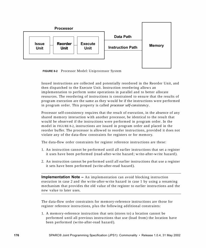
Issued instructions are collected and potentially reordered in the Reorder Unit, and then dispatched to the Execute Unit. Instruction reordering allows an implementation to perform some operations in parallel and to better allocate resources. The reordering of instructions is constrained to ensure that the results of program execution are the same as they would be if the instructions were performed in program order. This property is called processor self-consistency.
Processor self-consistency requires that the result of execution, in the absence of any shared memory interaction with another processor, be identical to the result that would be observed if the instructions were performed in program order. In the model in FIGURE 8-2, instructions are issued in program order and placed in the reorder buffer. The processor is allowed to reorder instructions, provided it does not violate any of the data-flow constraints for registers or for memory.
The data-flow order constraints for register reference instructions are these:
1. An instruction cannot be performed until all earlier instructions that set a register it uses have been performed (read-after-write hazard; write-after-write hazard).
2. An instruction cannot be performed until all earlier instructions that use a register it sets have been performed (write-after-read hazard).
Implementation Note – An implementation can avoid blocking instruction execution in case 2 and the write-after-write hazard in case 1 by using a renaming mechanism that provides the old value of the register to earlier instructions and the new value to later uses.
The data-flow order constraints for memory-reference instructions are those for register reference instructions, plus the following additional constraints:
1. A memory-reference instruction that sets (stores to) a location cannot be performed until all previous instructions that use (load from) the location have been performed (write-after-read hazard).
Processor
Memory
Data Path
Instruction PathIssue Reorder Execute
FIGURE 8-2 Processor Model: Uniprocessor System
Unit Unit UnitReorder
Unit
176 SPARC® Joint Programming Specification (JPS1): Commonality • Release 1.0.4, 31 May 2002
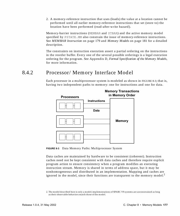
2. A memory-reference instruction that uses (loads) the value at a location cannot be performed until all earlier memory-reference instructions that set (store to) the location have been performed (read-after-write hazard).
Memory-barrier instructions (MEMBAR and STBAR) and the active memory model specified by PSTATE.MM also constrain the issue of memory-reference instructions. See MEMBAR Instruction on page 179 and Memory Models on page 181 for a detailed description.
The constraints on instruction execution assert a partial ordering on the instructions in the reorder buffer. Every one of the several possible orderings is a legal execution ordering for the program. See Appendix D, Formal Specification of the Memory Models, for more information.
8.4.2 Processor/Memory Interface ModelEach processor in a multiprocessor system is modeled as shown in FIGURE 8-3; that is, having two independent paths to memory: one for instructions and one for data.
FIGURE 8-3 Data Memory Paths: Multiprocessor System
Data caches are maintained by hardware to be consistent (coherent). Instruction caches need not be kept consistent with data caches and therefore require explicit program action to ensure consistency when a program modifies an executing instruction stream. Memory is shared in terms of address space, but it may be nonhomogeneous and distributed in an implementation. Mapping and caches are ignored in the model, since their functions are transparent to the memory model.2
2. The model described here is only a model; implementations of SPARC V9 systems are unconstrained as long as their observable behaviors match those of the model.
Processors
Memory Transactionsin Memory Order
Memory
Instructions
Data
Release 1.0.4, 31 May 2002 C. Chapter 8 • Memory Models 177
In real systems, addresses may have attributes that the processor must respect. The processor executes loads, stores, and atomic load-stores in whatever order it chooses, as constrained by program order and the current memory model. The ASI-address couples it generates are translated by a memory management unit (MMU), which associates attributes with the address and may, in some instances, abort the memory transaction and signal an exception to the CPU.
For example, a region of memory may be marked as nonprefetchable, noncacheable, read-only, or restricted. It is the MMU’s responsibility, working in conjunction with system software, to ensure that memory attribute constraints are not violated. See Appendix F of the Implementation Supplements for more information.
Instructions are performed in an order constrained by local dependencies. Using this dependency ordering, an execution unit submits one or more pending memory transactions to the memory. The memory performs transactions in memory order. The memory unit may perform transactions submitted to it out of order; hence, the execution unit must not concurrently submit two or more transactions that are required to be ordered.
The memory accepts transactions, performs them, and then acknowledges their completion. Multiple memory operations may be in progress at any time and may be initiated in a nondeterministic fashion in any order, provided that all transactions to a location preserve the per-processor partial orders. Memory transactions may complete in any order. Once initiated, all memory operations are performed atomically: loads from one location all see the same value, and the result of stores is visible to all potential requestors at the same instant.
The order of memory operations observed at a single location is a total order that preserves the partial orderings of each processor’s transactions to this address. There may be many legal total orders for a given program’s execution.
178 SPARC® Joint Programming Specification (JPS1): Commonality • Release 1.0.4, 31 May 2002
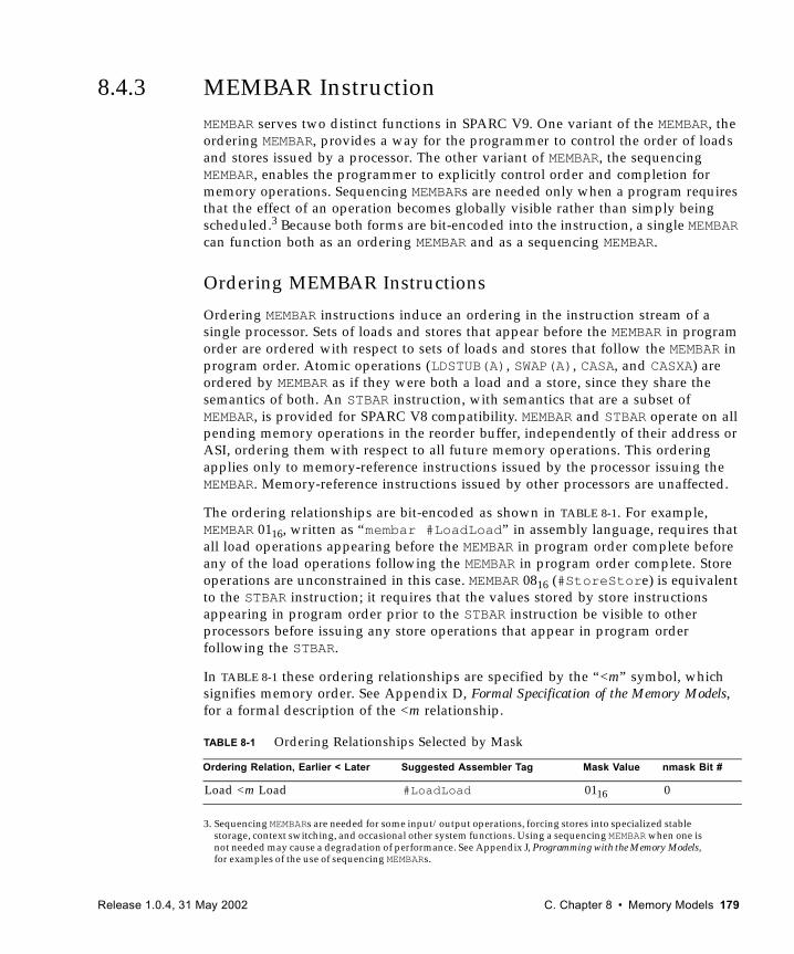
8.4.3 MEMBAR InstructionMEMBAR serves two distinct functions in SPARC V9. One variant of the MEMBAR, the ordering MEMBAR, provides a way for the programmer to control the order of loads and stores issued by a processor. The other variant of MEMBAR, the sequencing MEMBAR, enables the programmer to explicitly control order and completion for memory operations. Sequencing MEMBARs are needed only when a program requires that the effect of an operation becomes globally visible rather than simply being scheduled.3 Because both forms are bit-encoded into the instruction, a single MEMBAR can function both as an ordering MEMBAR and as a sequencing MEMBAR.
Ordering MEMBAR Instructions
Ordering MEMBAR instructions induce an ordering in the instruction stream of a single processor. Sets of loads and stores that appear before the MEMBAR in program order are ordered with respect to sets of loads and stores that follow the MEMBAR in program order. Atomic operations (LDSTUB(A), SWAP(A), CASA, and CASXA) are ordered by MEMBAR as if they were both a load and a store, since they share the semantics of both. An STBAR instruction, with semantics that are a subset of MEMBAR, is provided for SPARC V8 compatibility. MEMBAR and STBAR operate on all pending memory operations in the reorder buffer, independently of their address or ASI, ordering them with respect to all future memory operations. This ordering applies only to memory-reference instructions issued by the processor issuing the MEMBAR. Memory-reference instructions issued by other processors are unaffected.
The ordering relationships are bit-encoded as shown in TABLE 8-1. For example, MEMBAR 0116, written as “membar #LoadLoad” in assembly language, requires that all load operations appearing before the MEMBAR in program order complete before any of the load operations following the MEMBAR in program order complete. Store operations are unconstrained in this case. MEMBAR 0816 (#StoreStore) is equivalent to the STBAR instruction; it requires that the values stored by store instructions appearing in program order prior to the STBAR instruction be visible to other processors before issuing any store operations that appear in program order following the STBAR.
In TABLE 8-1 these ordering relationships are specified by the “<m” symbol, which signifies memory order. See Appendix D, Formal Specification of the Memory Models, for a formal description of the <m relationship.
3. Sequencing MEMBARs are needed for some input/output operations, forcing stores into specialized stable storage, context switching, and occasional other system functions. Using a sequencing MEMBAR when one is not needed may cause a degradation of performance. See Appendix J, Programming with the Memory Models, for examples of the use of sequencing MEMBARs.
TABLE 8-1 Ordering Relationships Selected by Mask
Ordering Relation, Earlier < Later Suggested Assembler Tag Mask Value nmask Bit #
Load <m Load #LoadLoad 0116 0
Release 1.0.4, 31 May 2002 C. Chapter 8 • Memory Models 179
Selections may be combined to form more powerful barriers. For example, a MEMBAR instruction with a mask of 0916 (#LoadLoad | #StoreStore) orders loads with respect to loads and stores with respect to stores, but it does not order loads with respect to stores, or vice versa.
Sequencing MEMBAR Instructions
A sequencing MEMBAR exerts explicit control over the completion of operations. The three sequencing MEMBAR options each have a different degree of control and a different application.
■ Lookaside Barrier — Ensures that loads following this MEMBAR are from memory and not from a lookaside into a write buffer. Lookaside Barrier requires that pending stores issued prior to the MEMBAR be completed before any load from that address following the MEMBAR may be issued. A Lookaside Barrier MEMBAR may be needed to provide lock fairness and to support some plausible I/O location semantics. See the example in J.14.2, The Control and Status Register (CSR).
■ Memory Issue Barrier — Ensures that all memory operations appearing in program order before the sequencing MEMBAR complete before any new memory operation may be initiated. See the example in J.14.1, I/O Registers with Side Effects.
■ Synchronization Barrier — Ensures that all instructions (memory reference and others) preceding the MEMBAR complete and that the effects of any fault or error have become visible before any instruction following the MEMBAR in program order is initiated. A Synchronization Barrier MEMBAR fully synchronizes the processor that issues it.
TABLE 8-2 shows the encoding of these functions in the MEMBAR instruction.
Store <m Load #StoreLoad 0216 1
Load <m Store #LoadStore 0416 2
Store <m Store #StoreStore 0816 3
TABLE 8-2 Sequencing Barrier Selected by Mask
Sequencing Function Assembler Tag Mask Value cmask Bit #
Lookaside Barrier #Lookaside 1016 0
Memory Issue Barrier #MemIssue 2016 1
Synchronization Barrier #Sync 4016 2
TABLE 8-1 Ordering Relationships Selected by Mask
Ordering Relation, Earlier < Later Suggested Assembler Tag Mask Value nmask Bit #
180 SPARC® Joint Programming Specification (JPS1): Commonality • Release 1.0.4, 31 May 2002
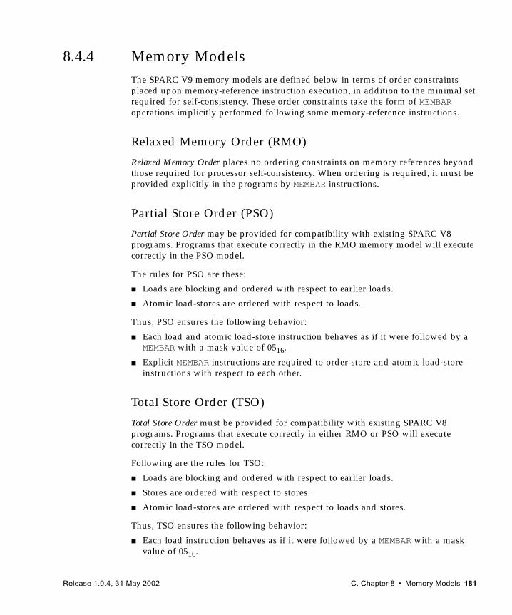
8.4.4 Memory ModelsThe SPARC V9 memory models are defined below in terms of order constraints placed upon memory-reference instruction execution, in addition to the minimal set required for self-consistency. These order constraints take the form of MEMBAR operations implicitly performed following some memory-reference instructions.
Relaxed Memory Order (RMO)
Relaxed Memory Order places no ordering constraints on memory references beyond those required for processor self-consistency. When ordering is required, it must be provided explicitly in the programs by MEMBAR instructions.
Partial Store Order (PSO)
Partial Store Order may be provided for compatibility with existing SPARC V8 programs. Programs that execute correctly in the RMO memory model will execute correctly in the PSO model.
The rules for PSO are these:
■ Loads are blocking and ordered with respect to earlier loads.
■ Atomic load-stores are ordered with respect to loads.
Thus, PSO ensures the following behavior:
■ Each load and atomic load-store instruction behaves as if it were followed by a MEMBAR with a mask value of 0516.
■ Explicit MEMBAR instructions are required to order store and atomic load-store instructions with respect to each other.
Total Store Order (TSO)
Total Store Order must be provided for compatibility with existing SPARC V8 programs. Programs that execute correctly in either RMO or PSO will execute correctly in the TSO model.
Following are the rules for TSO:
■ Loads are blocking and ordered with respect to earlier loads.
■ Stores are ordered with respect to stores.
■ Atomic load-stores are ordered with respect to loads and stores.
Thus, TSO ensures the following behavior:
■ Each load instruction behaves as if it were followed by a MEMBAR with a mask value of 0516.
Release 1.0.4, 31 May 2002 C. Chapter 8 • Memory Models 181
■ Each store instruction behaves as if it were followed by a MEMBAR with a mask of 0816.
■ Each atomic load-store behaves as if it were followed by a MEMBAR with a mask of 0D16.
8.4.5 Mode ControlThe memory model is specified by the 2-bit state in PSTATE.MM, described in PSTATE_mem_model (MM) on page 71.
Writing a new value into PSTATE.MM causes subsequent memory reference instructions to be performed with the order constraints of the specified memory model.
SPARC V9 processors need not provide all three memory models; undefined values of PSTATE.MM have implementation-dependent effects.
IMPL. DEP. #119: The effect of writing an unimplemented memory mode designation into PSTATE.MM is implementation dependent.
Except when a trap enters RED_state, PSTATE.MM is left unchanged when a trap is entered and the old value is stacked. When RED_state is entered, the value of PSTATE.MM is set to TSO.
8.4.6 Hardware Primitives for Mutual ExclusionIn addition to providing memory-ordering primitives that allow programmers to construct mutual-exclusion mechanisms in software, SPARC V9 provides three hardware primitives for mutual exclusion:
■ Compare and Swap (CASA and CASXA)■ Load Store Unsigned Byte (LDSTUB and LDSTUBA)■ Swap (SWAP and SWAPA)
Each of these instructions has the semantics of both a load and a store in all three memory models. They are all atomic, in the sense that no other store to the same location can be performed between the load and store elements of the instruction. All of the hardware mutual-exclusion operations conform to the memory models and may require barrier instructions to ensure proper data visibility.
When the hardware mutual-exclusion primitives address I/O locations, the results are implementation dependent. In addition, the atomicity of hardware mutual-exclusion primitives is guaranteed only for processor memory references and not when the memory location is simultaneously being addressed by an I/O device such as a channel or DMA.
182 SPARC® Joint Programming Specification (JPS1): Commonality • Release 1.0.4, 31 May 2002
Compare-and-Swap (CASA, CASXA)
Compare-and-swap is an atomic operation that compares a value in a processor register to a value in memory and, if and only if they are equal, swaps the value in memory with the value in a second processor register. Both 32-bit (CASA) and 64-bit (CASXA) operations are provided. The compare-and-swap operation is atomic in the sense that once it begins, no other processor can access the memory location specified until the compare has completed and the swap (if any) has also completed and is potentially visible to all other processors in the system.
Compare-and-swap is substantially more powerful than the other hardware synchronization primitives. It has an infinite consensus number; that is, it can resolve, in a wait-free fashion, an infinite number of contending processes. Because of this property, compare-and-swap can be used to construct wait-free algorithms that do not require the use of locks. See Appendix J, Programming with the Memory Models, for examples.
Swap (SWAP)
SWAP atomically exchanges the lower 32 bits in a processor register with a word in memory. SWAP has a consensus number of two; that is, it cannot resolve more than two contending processes in a wait-free fashion.
Load Store Unsigned Byte (LDSTUB)
LDSTUB loads a byte value from memory to a register and writes the value FF16 into the addressed byte atomically. LDSTUB is the classic test-and-set instruction. Like SWAP, it has a consensus number of two and so cannot resolve more than two contending processes in a wait-free fashion.
8.4.7 Synchronizing Instruction and Data MemoryThe SPARC V9 memory models do not require that instruction and data memory images be consistent at all times. The instruction and data memory images may become inconsistent if a program writes into the instruction stream. As a result, whenever instructions are modified by a program in a context where the data (that is, the instructions) in the memory and the data cache hierarchy may be inconsistent with instructions in the instruction cache hierarchy, some special programmatic action must be taken.
The FLUSH instruction will ensure consistency between the in-flight instruction stream and the data references in the processor executing FLUSH. The programmer must ensure that the modification sequence is robust under multiple updates and
Release 1.0.4, 31 May 2002 C. Chapter 8 • Memory Models 183
concurrent execution. Since, in general, loads and stores may be performed out of order, appropriate MEMBAR and FLUSH instructions must be interspersed as needed to control the order in which the instruction data are mutated.
The FLUSH instruction ensures that subsequent instruction fetches from the doubleword target of the FLUSH by the processor executing the FLUSH appear to execute after any loads, stores, and atomic load-stores issued by the processor to that address prior to the FLUSH. FLUSH acts as a barrier for instruction fetches in the processor on which it executes and has the properties of a store with respect to MEMBAR operations.
FLUSH has zero latency on the issuing processor; the modified instruction stream is immediately available.4
IMPL. DEP. #122: The latency between the execution of FLUSH on one processor and the point at which the modified instructions have replaced outdated instructions in a multiprocessor is implementation dependent.
Programming Note – Because FLUSH is designed to act on a doubleword and because, on some implementations, FLUSH may trap to system software, it is recommended that system software provide a user-callable service routine for flushing arbitrarily sized regions of memory. On some implementations, this routine would issue a series of FLUSH instructions; on others, it might issue a single trap to system software that would then flush the entire region.
On a SPARC JPS1 processor:
■ A FLUSH instruction flushes the processor pipeline and synchronizes the processor.
■ Coherency between instruction and data memories is maintained with hardware; therefore, the address in the operands of a FLUSH instruction may be ignored (but must be supplied by software for SPARC V9 compatibility).
Programming Note – Although SPARC JPS1 processors maintain coherency between instruction and data caches in hardware, SPARC V9 implementations in general are not required to do so (and some do not). Therefore, portable SPARC V9 software:(1) must always assume that store instructions (except Block Store with Commit) do not coherently update I-cache(s);(2) must, in every FLUSH instruction, supply the address of the instruction or instructions that were modified.
4. SPARC V8 specified a five-instruction latency. Invalidation of instructions in the instruction cache during their execution is likely to force an instruction-cache fault.
184 SPARC® Joint Programming Specification (JPS1): Commonality • Release 1.0.4, 31 May 2002
C.APPENDIX A
Instruction Definitions
The SPARC Joint Programming Specification extends the standard SPARC V9 instruction set with four classes of instructions:
■ Low-power mode: SHUTDOWN (A.59)
■ Enhanced graphics functionality: instructions for alignment (A.2); array handling (A.3); BMASK and BSHUFFLE (A.5); edge handling (A.12); logical operations on floating-point registers (A.33); and partitioned arithmetic and pixel manipulation (A.43 to A.47)
■ Efficient memory access: partial store (A.42); short floating-point loads and stores (A.58); atomic load quadword (A.30); and block load and store (A.4)
■ Efficient interval arithmetic: SIAM (A.55) and all instructions that reference GSR.IM
Related instructions are grouped into subsections. Each subsection consists of these parts:
1. A table of the opcodes defined in the subsection with the values of the field(s) that uniquely identify the instruction(s).
2. An illustration of the applicable instruction format(s). In these illustrations a dash (—) indicates that the field is reserved for future versions of the architecture and shall be 0 in any instance of the instruction. If a conforming SPARC V9 implementation encounters nonzero values in these fields, its behavior is undefined. See Appendix I, Extending the SPARC V9 Architecture, for information about extending the SPARC V9 instruction set.
3. A list of the suggested assembly language syntax; the syntax notation is described in Appendix G, Assembly Language Syntax.
4. A description of the features, restrictions, and exception-causing conditions.
5. A list of exceptions that can occur as a consequence of attempting to execute the instruction(s). Exceptions due to an instruction_access_error, instruction_access_exception, fast_instruction_access_MMU_miss, fast_ECC_error†, async_data_error†, ECC_error (corrected ECC_error), WDR, and interrupts are not listed because they can occur on any instruction. A
Release 1.0.4, 31 May 2002 C. Appendix A • Instruction Definitions 185
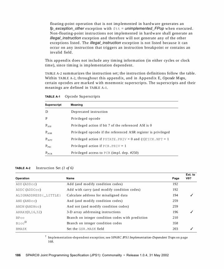
floating-point operation that is not implemented in hardware generates an fp_exception_other exception with ftt = unimplemented_FPop when executed. Non-floating-point instructions not implemented in hardware shall generate an illegal_instruction exception and therefore will not generate any of the other exceptions listed. The illegal_instruction exception is not listed because it can occur on any instruction that triggers an instruction breakpoint or contains an invalid field.
This appendix does not include any timing information (in either cycles or clock time), since timing is implementation dependent.
TABLE A-2 summarizes the instruction set; the instruction definitions follow the table. Within TABLE A-2, throughout this appendix, and in Appendix E, Opcode Maps, certain opcodes are marked with mnemonic superscripts. The superscripts and their meanings are defined in TABLE A-1.
† Implementation-dependent exception; see SPARC JPS1 Implementation-Dependent Traps on page 168.
TABLE A-1 Opcode Superscripts
Superscript Meaning
D Deprecated instruction
P Privileged opcode
PASI Privileged action if bit 7 of the referenced ASI is 0
PASR Privileged opcode if the referenced ASR register is privileged
PNPT Privileged action if PSTATE.PRIV = 0 and (S)TICK.NPT = 1
PPIC Privileged action if PCR.PRIV = 1
PPCR Privileged access to PCR (impl. dep. #250)
TABLE A-2 Instruction Set (1 of 6)
Operation Name PageExt. to V9?
ADD (ADDcc) Add (and modify condition codes) 192
ADDC (ADDCcc) Add with carry (and modify condition codes) 192
ALIGNADDRESS{_LITTLE} Calculate address for misaligned data 194 ✓
AND (ANDcc) And (and modify condition codes) 259
ANDN (ANDNcc) And not (and modify condition codes) 259
ARRAY(8,16,32) 3-D array addressing instructions 196 ✓
BPcc Branch on integer condition codes with prediction 210
BiccD Branch on integer condition codes 358
BMASK Set the GSR.MASK field 203 ✓
186 SPARC® Joint Programming Specification (JPS1): Commonality • Release 1.0.4, 31 May 2002
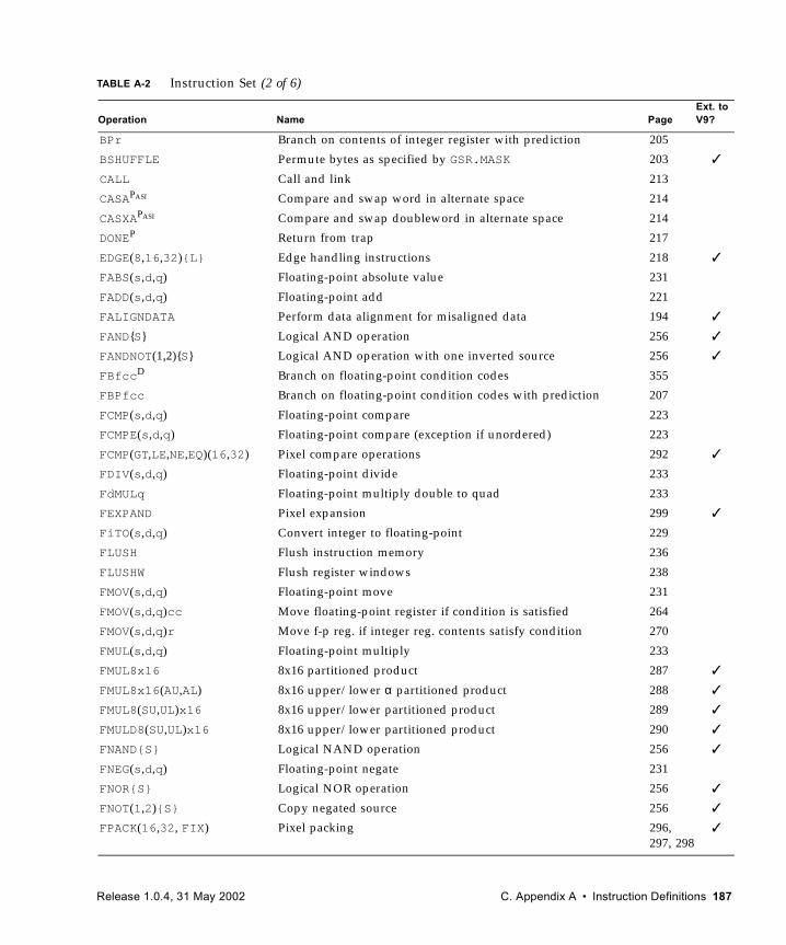
BPr Branch on contents of integer register with prediction 205
BSHUFFLE Permute bytes as specified by GSR.MASK 203 ✓
CALL Call and link 213
CASAPASI Compare and swap word in alternate space 214
CASXAPASI Compare and swap doubleword in alternate space 214
DONEP Return from trap 217
EDGE(8,16,32){L} Edge handling instructions 218 ✓
FABS(s,d,q) Floating-point absolute value 231
FADD(s,d,q) Floating-point add 221
FALIGNDATA Perform data alignment for misaligned data 194 ✓
FAND{S} Logical AND operation 256 ✓
FANDNOT(1,2){S} Logical AND operation with one inverted source 256 ✓
FBfccD Branch on floating-point condition codes 355
FBPfcc Branch on floating-point condition codes with prediction 207
FCMP(s,d,q) Floating-point compare 223
FCMPE(s,d,q) Floating-point compare (exception if unordered) 223
FCMP(GT,LE,NE,EQ)(16,32) Pixel compare operations 292 ✓
FDIV(s,d,q) Floating-point divide 233
FdMULq Floating-point multiply double to quad 233
FEXPAND Pixel expansion 299 ✓
FiTO(s,d,q) Convert integer to floating-point 229
FLUSH Flush instruction memory 236
FLUSHW Flush register windows 238
FMOV(s,d,q) Floating-point move 231
FMOV(s,d,q)cc Move floating-point register if condition is satisfied 264
FMOV(s,d,q)r Move f-p reg. if integer reg. contents satisfy condition 270
FMUL(s,d,q) Floating-point multiply 233
FMUL8x16 8x16 partitioned product 287 ✓
FMUL8x16(AU,AL) 8x16 upper/lower α partitioned product 288 ✓
FMUL8(SU,UL)x16 8x16 upper/lower partitioned product 289 ✓
FMULD8(SU,UL)x16 8x16 upper/lower partitioned product 290 ✓
FNAND{S} Logical NAND operation 256 ✓
FNEG(s,d,q) Floating-point negate 231
FNOR{S} Logical NOR operation 256 ✓
FNOT(1,2){S} Copy negated source 256 ✓
FPACK(16,32, FIX) Pixel packing 296, 297, 298
✓
TABLE A-2 Instruction Set (2 of 6)
Operation Name PageExt. to V9?
Release 1.0.4, 31 May 2002 C. Appendix A • Instruction Definitions 187
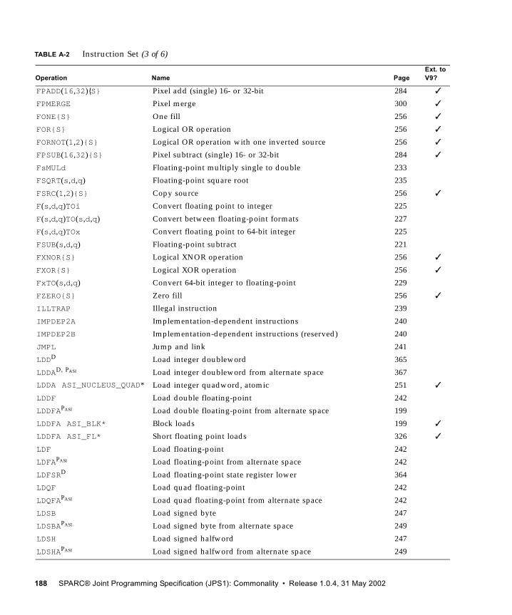
FPADD(16,32){S} Pixel add (single) 16- or 32-bit 284 ✓
FPMERGE Pixel merge 300 ✓
FONE{S} One fill 256 ✓
FOR{S} Logical OR operation 256 ✓
FORNOT(1,2){S} Logical OR operation with one inverted source 256 ✓
FPSUB(16,32){S} Pixel subtract (single) 16- or 32-bit 284 ✓
FsMULd Floating-point multiply single to double 233
FSQRT(s,d,q) Floating-point square root 235
FSRC(1,2){S} Copy source 256 ✓
F(s,d,q)TOi Convert floating point to integer 225
F(s,d,q)TO(s,d,q) Convert between floating-point formats 227
F(s,d,q)TOx Convert floating point to 64-bit integer 225
FSUB(s,d,q) Floating-point subtract 221
FXNOR{S} Logical XNOR operation 256 ✓
FXOR{S} Logical XOR operation 256 ✓
FxTO(s,d,q) Convert 64-bit integer to floating-point 229
FZERO{S} Zero fill 256 ✓
ILLTRAP Illegal instruction 239
IMPDEP2A Implementation-dependent instructions 240
IMPDEP2B Implementation-dependent instructions (reserved) 240
JMPL Jump and link 241
LDDD Load integer doubleword 365
LDDAD, PASI Load integer doubleword from alternate space 367
LDDA ASI_NUCLEUS_QUAD* Load integer quadword, atomic 251 ✓
LDDF Load double floating-point 242
LDDFAPASI Load double floating-point from alternate space 199
LDDFA ASI_BLK* Block loads 199 ✓
LDDFA ASI_FL* Short floating point loads 326 ✓
LDF Load floating-point 242
LDFAPASI Load floating-point from alternate space 242
LDFSRD Load floating-point state register lower 364
LDQF Load quad floating-point 242
LDQFAPASI Load quad floating-point from alternate space 242
LDSB Load signed byte 247
LDSBAPASI Load signed byte from alternate space 249
LDSH Load signed halfword 247
LDSHAPASI Load signed halfword from alternate space 249
TABLE A-2 Instruction Set (3 of 6)
Operation Name PageExt. to V9?
188 SPARC® Joint Programming Specification (JPS1): Commonality • Release 1.0.4, 31 May 2002
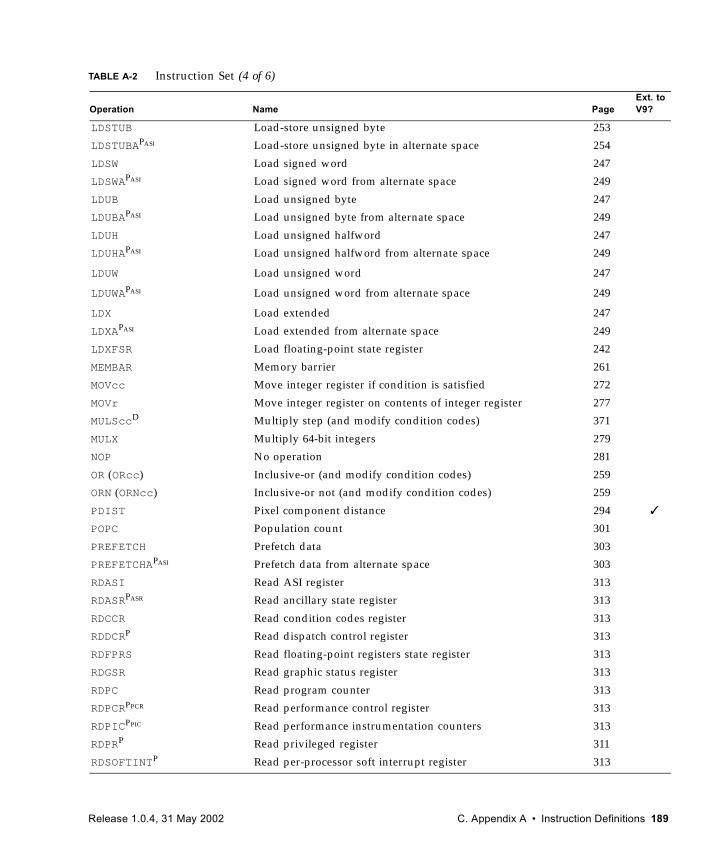
LDSTUB Load-store unsigned byte 253
LDSTUBAPASI Load-store unsigned byte in alternate space 254
LDSW Load signed word 247
LDSWAPASI Load signed word from alternate space 249
LDUB Load unsigned byte 247
LDUBAPASI Load unsigned byte from alternate space 249
LDUH Load unsigned halfword 247
LDUHAPASI Load unsigned halfword from alternate space 249
LDUW Load unsigned word 247
LDUWAPASI Load unsigned word from alternate space 249
LDX Load extended 247
LDXAPASI Load extended from alternate space 249
LDXFSR Load floating-point state register 242
MEMBAR Memory barrier 261
MOVcc Move integer register if condition is satisfied 272
MOVr Move integer register on contents of integer register 277
MULSccD Multiply step (and modify condition codes) 371
MULX Multiply 64-bit integers 279
NOP No operation 281
OR (ORcc) Inclusive-or (and modify condition codes) 259
ORN (ORNcc) Inclusive-or not (and modify condition codes) 259
PDIST Pixel component distance 294 ✓
POPC Population count 301
PREFETCH Prefetch data 303
PREFETCHAPASI Prefetch data from alternate space 303
RDASI Read ASI register 313
RDASRPASR Read ancillary state register 313
RDCCR Read condition codes register 313
RDDCRP Read dispatch control register 313
RDFPRS Read floating-point registers state register 313
RDGSR Read graphic status register 313
RDPC Read program counter 313
RDPCRPPCR Read performance control register 313
RDPICPPIC Read performance instrumentation counters 313
RDPRP Read privileged register 311
RDSOFTINTP Read per-processor soft interrupt register 313
TABLE A-2 Instruction Set (4 of 6)
Operation Name PageExt. to V9?
Release 1.0.4, 31 May 2002 C. Appendix A • Instruction Definitions 189
RDSTICKPNPT Read system TICK register 313
RDSTICK_CMPRP Read system TICK compare register 313
RDTICKPNPT Read TICK register 313
RDTICK_CMPRP Read TICK compare register 313
RDYD Read Y register 373
RESTORE Restore caller’s window 318
RESTOREDP Window has been restored 321
RETRYP Return from trap and retry 217
RETURN Return 316
SAVE Save caller’s window 318
SAVEDP Window has been saved 321
SDIVD (SDIVccD) 32-bit signed integer divide (and modify condition codes) 361
SDIVX 64-bit signed integer divide 279
SETHI Set high 22 bits of low word of integer register 323
SHUTDOWN Shut down the processor 328 ✓
SIAM Set Interval Arithmetic Mode 322 ✓
SIR Software-initiated reset 329
SLL Shift left logical 324
SLLX Shift left logical, extended 324
SMULD (SMULccD) Signed integer multiply (and modify condition codes) 369
SRA Shift right arithmetic 324
SRAX Shift right arithmetic, extended 324
SRL Shift right logical 324
SRLX Shift right logical, extended 324
STB Store byte 336
STBAPASI Store byte into alternate space 338
STBARD Store barrier 374
STDD Store doubleword 377
STDAD, PASI Store doubleword into alternate space 379
STDF Store double floating-point 330
STDFAPASI Store double floating-point into alternate space 333
STDFA ASI_BLK* Block stores 199 ✓
STDFA ASI_FL* Short floating point stores 326 ✓
STDFA ASI_PST* Partial Store instructions 282 ✓
STF Store floating-point 330
STFAPASI Store floating-point into alternate space 333
STFSRD Store floating-point state register 375
TABLE A-2 Instruction Set (5 of 6)
Operation Name PageExt. to V9?
190 SPARC® Joint Programming Specification (JPS1): Commonality • Release 1.0.4, 31 May 2002
STH Store halfword 336
STHAPASI Store halfword into alternate space 338
STQF Store quad floating-point 330
STQFAPASI Store quad floating-point into alternate space 333
STW Store word 336
STWAPASI Store word into alternate space 338
STX Store extended 336
STXAPASI Store extended into alternate space 338
STXFSR Store extended floating-point state register 330
SUB (SUBcc) Subtract (and modify condition codes) 340
SUBC (SUBCcc) Subtract with carry (and modify condition codes) 340
SWAPD Swap integer register with memory 381
SWAPAD, PASI Swap integer register with memory in alternate space 383
TADDcc (TADDccTVD) Tagged add and modify condition codes (trap on overflow) 342, 385
Tcc Trap on integer condition codes 344
TSUBcc (TSUBccTVD) Tagged subtract and modify condition codes (trap on overflow) 343, 387
UDIVD (UDIVccD) Unsigned integer divide (and modify condition codes) 361
UDIVX 64-bit unsigned integer divide 279
UMULD (UMULccD) Unsigned integer multiply (and modify condition codes) 369
WRASI Write ASI register 350
WRASRPASR Write ancillary state register 350
WRCCR Write condition codes register 350
WRDCRP Write dispatch control register 350
WRFPRS Write floating-point registers state register 350
WRGSR Write graphic status register 350
WRPCRPPCR Write performance control register 350
WRPICPPIC Write performance instrumentation counters register 350
WRPRP Write privileged register 347
WRSOFTINTP Write per-processor soft interrupt register 350
WRSOFTINT_CLRP Clear bits of per-processor soft interrupt register 350
WRSOFTINT_SETP Set bits of per-processor soft interrupt register 350
WRTICK_CMPRP Write TICK compare register 350
WRSTICKP Write System TICK register 350
WRSTICK_CMPRP Write System TICK compare register 350
WRYD Write Y register 389
XNOR (XNORcc) Exclusive-nor (and modify condition codes) 259
XOR (XORcc) Exclusive-or (and modify condition codes) 259
TABLE A-2 Instruction Set (6 of 6)
Operation Name PageExt. to V9?
Release 1.0.4, 31 May 2002 C. Appendix A • Instruction Definitions 191
Add
A.1 Add
Format (3)
Description: ADD and ADDcc compute “r[rs1] + r[rs2]” if i = 0, or “r[rs1] + sign_ext(simm13)” if i = 1, and write the sum into r[rd].
ADDC and ADDCcc (“ADD with carry”) also add the CCR register’s 32-bit carry (icc.c) bit; that is, they compute “r[rs1] + r[rs2] + icc.c” or “r[rs1] + sign_ext(simm13) + icc.c” and write the sum into r[rd].
ADDcc and ADDCcc modify the integer condition codes (CCR.icc and CCR.xcc). Overflow occurs on addition if both operands have the same sign and the sign of the sum is different.
Opcode Op3 Operation
ADD 00 0000 Add
ADDcc 01 0000 Add and modify cc’s
ADDC 00 1000 Add with Carry
ADDCcc 01 1000 Add with Carry and modify cc’s
Assembly Language Syntax
add regrs1, reg_or_imm, regrd
addcc regrs1, reg_or_imm, regrd
addc regrs1, reg_or_imm, regrd
addccc regrs1, reg_or_imm, regrd
31 24 02530 29 19 18
rd10 op3 —
14 13 12 5 4
rs1 rs2i=0
rd10 op3 rs1 simm13i=1
192 SPARC® Joint Programming Specification (JPS1): Commonality • Release 1.0.4, 31 May 2002
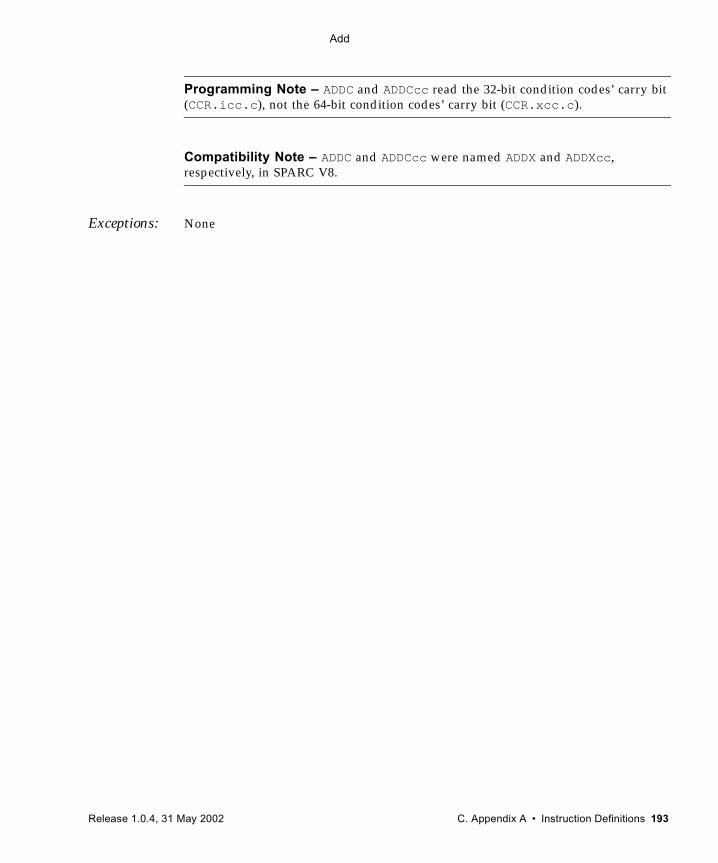
Add
Programming Note – ADDC and ADDCcc read the 32-bit condition codes’ carry bit (CCR.icc.c), not the 64-bit condition codes’ carry bit (CCR.xcc.c).
Compatibility Note – ADDC and ADDCcc were named ADDX and ADDXcc, respectively, in SPARC V8.
Exceptions: None
Release 1.0.4, 31 May 2002 C. Appendix A • Instruction Definitions 193
Alignment Instructions (VIS I)
A.2 Alignment Instructions (VIS I)
Format (3)
Description: ALIGNADDRESS adds two integer values, r[rs1] and r[rs2], and stores the result (with the least significant 3 bits forced to 0) in the integer register r[rd]. The least significant 3 bits of the result are stored in the GSR.align field.
ALIGNADDRESS_LITTLE is the same as ALIGNADDRESS except that the 2’s complement of the least significant 3 bits of the result is stored in GSR.align.
Note – ALIGNADDR_LITTLE generates the opposite-endian byte ordering for a subsequent FALIGNDATA operation.
FALIGNDATA concatenates the two 64-bit floating-point registers specified by rs1 and rs2 to form a 128-bit (16-byte) intermediate value. The contents of the first source operand form the more-significant 8 bytes of the intermediate value, and the contents of the second source operand form the less significant 8 bytes of the intermediate value. Bytes in the intermediate value are numbered from most significant (byte 0) to least significant (byte 15). Eight bytes are extracted from the
Opcode opf Operation
ALIGNADDRESS 0 0001 1000 Calculate address for misaligned data access
ALIGNADDRESS_LITTLE 0 0001 1010 Calculate address for misaligned data access little-endian
FALIGNDATA 0 0100 1000 Perform data alignment for misaligned data
Assembly Language Syntax
alignaddr regrs1, regrs2, regrd
alignaddrl regrs1, regrs2, regrd
faligndata fregrs1, fregrs2, fregrd
31 24 02530 29 19 18 14 13 5 4
rd10 110110 opfrs1 rs2
194 SPARC® Joint Programming Specification (JPS1): Commonality • Release 1.0.4, 31 May 2002
Alignment Instructions (VIS I)
intermediate value and stored in the 64-bit floating-point destination register specified by rd. GSR.align specifies the number of the most significant byte to extract (and, therefore, the least significant byte extracted from the intermediate value is numbered GSR.align+7).
A byte-aligned 64-bit load can be performed as shown in CODE EXAMPLE A-1.
Exceptions: fp_disabled
CODE EXAMPLE A-1 Byte-Aligned 64-Bit Load
alignaddr Address, Offset, Address
ldd [Address], %f0
ldd [Address + 8], %f2
faligndata %f0, %f2, %f4
Release 1.0.4, 31 May 2002 C. Appendix A • Instruction Definitions 195
Three-Dimensional Array Addressing Instructions (VIS I)
A.3 Three-Dimensional Array Addressing Instructions (VIS I)
Format (3)
Description These instructions convert three-dimensional (3D) fixed-point addresses contained in r[rs1] to a blocked-byte address; they store the result in r[rd]. Fixed-point addresses typically are used for address interpolation for planar reformatting operations. Blocking is performed at the 64-byte level to maximize external cache block reuse, and at the 64-Kbyte level to maximize TLB entry reuse, regardless of the orientation of the address interpolation. These instructions specify an element size of 8 bits (ARRAY8), 16 bits (ARRAY16), or 32 bits (ARRAY32). The second operand, r[rs2], specifies the power-of-2 size of the X and Y dimensions of a 3D image array. The legal values for rs2 and their meanings are shown in TABLE A-3. Illegal values produce undefined results in the destination register, r[rd].
Opcode opf Operation
ARRAY8 0 0001 0000 Convert 8-bit 3D address to blocked byte address
ARRAY16 0 0001 0010 Convert 16-bit 3D address to blocked byte address
ARRAY32 0 0001 0100 Convert 32-bit 3D address to blocked byte address
Assembly Language Syntax
array8 regrs1, regrs2, regrd
array16 regrs1, regrs2, regrd
array32 regrs1, regrs2, regrd
TABLE A-3 3D r[rs2] Array X/Y Dimensions
r[rs2] value Number of elements
0 64
1 128
31 24 02530 29 19 18 14 13 5 4
rd10 110110 opfrs1 rs2
196 SPARC® Joint Programming Specification (JPS1): Commonality • Release 1.0.4, 31 May 2002
Three-Dimensional Array Addressing Instructions (VIS I)
FIGURE A-1 Three-Dimensional Array Fixed-Point Address Format
The integer parts of X, Y, and Z are converted to the following blocked-address formats.
FIGURE A-2 Three-Dimensional Array Blocked-Address Format (Array8)
FIGURE A-3 Three-Dimensional Array Blocked-Address Format (Array16)
FIGURE A-4 Three Dimensional Array Blocked-Address Format (Array32)
2 256
3 512
4 1024
5 2048
TABLE A-3 3D r[rs2] Array X/Y Dimensions (Continued)
r[rs2] value Number of elements
0323363 55 54 44 43 22 21 11 10
X fractionX integerY fractionY integerZ fractionZ integer
04 2
XYZ
Lower
513 9
XYZ
Middle
1717 17
XYZ
Upper
+ isrc2+ 2 isrc220+ 2 isrc2
15 3
XYZ
Lower
614 10
XYZ
Middle
1818 18
XYZ
Upper
+ isrc2+ 2 isrc221+ 2 isrc2
0
0
26 4
XYZ
Lower
715 11
XYZ
Middle
1919 19
XYZ
Upper
+ isrc2+ 2 isrc222+ 2 isrc2
00
0
Release 1.0.4, 31 May 2002 C. Appendix A • Instruction Definitions 197
Three-Dimensional Array Addressing Instructions (VIS I)
The bits above Z upper are set to 0. The number of zeroes in the least significant bits is determined by the element size. An element size of 8 bits has no zeroes, an element size of 16 bits has one zero, and an element size of 32 bits has two zeroes. Bits in X and Y above the size specified by r[rs2] are ignored.
The code fragment in CODE EXAMPLE A-2 shows assembly of components along an interpolated line at the rate of one component per clock.
Exceptions None
CODE EXAMPLE A-2 Assembly of Components Along an Interpolated Line
add Addr, DeltaAddr, Addr
array8 Addr, %g0, bAddr
ldda [bAddr] ASI_FL8_PRIMARY, data
faligndata data, accum, accum
198 SPARC® Joint Programming Specification (JPS1): Commonality • Release 1.0.4, 31 May 2002
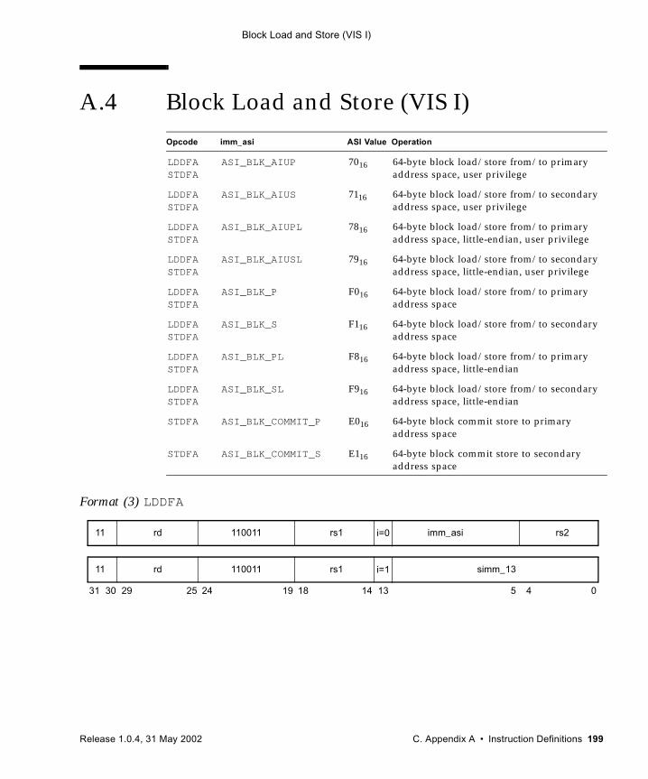
Block Load and Store (VIS I)
A.4 Block Load and Store (VIS I)
Format (3) LDDFA
Opcode imm_asi ASI Value Operation
LDDFASTDFA
ASI_BLK_AIUP 7016 64-byte block load/store from/to primary address space, user privilege
LDDFASTDFA
ASI_BLK_AIUS 7116 64-byte block load/store from/to secondary address space, user privilege
LDDFASTDFA
ASI_BLK_AIUPL 7816 64-byte block load/store from/to primary address space, little-endian, user privilege
LDDFASTDFA
ASI_BLK_AIUSL 7916 64-byte block load/store from/to secondary address space, little-endian, user privilege
LDDFASTDFA
ASI_BLK_P F016 64-byte block load/store from/to primary address space
LDDFASTDFA
ASI_BLK_S F116 64-byte block load/store from/to secondary address space
LDDFASTDFA
ASI_BLK_PL F816 64-byte block load/store from/to primary address space, little-endian
LDDFASTDFA
ASI_BLK_SL F916 64-byte block load/store from/to secondary address space, little-endian
STDFA ASI_BLK_COMMIT_P E016 64-byte block commit store to primary address space
STDFA ASI_BLK_COMMIT_S E116 64-byte block commit store to secondary address space
31 24 02530 29 19 18 14 13 5 4
rd11 110011 simm_13rs1 i=1
rd11 110011 imm_asirs1 rs2i=0
Release 1.0.4, 31 May 2002 C. Appendix A • Instruction Definitions 199
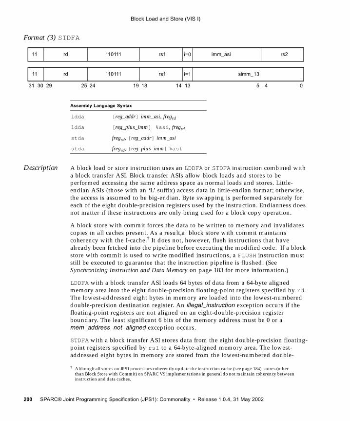
Block Load and Store (VIS I)
Format (3) STDFA
Description A block load or store instruction uses an LDDFA or STDFA instruction combined with a block transfer ASI. Block transfer ASIs allow block loads and stores to be performed accessing the same address space as normal loads and stores. Little-endian ASIs (those with an ‘L’ suffix) access data in little-endian format; otherwise, the access is assumed to be big-endian. Byte swapping is performed separately for each of the eight double-precision registers used by the instruction. Endianness does not matter if these instructions are only being used for a block copy operation.
A block store with commit forces the data to be written to memory and invalidates copies in all caches present. As a result,a block store with commit maintains coherency with the I-cache.† It does not, however, flush instructions that have already been fetched into the pipeline before executing the modified code. If a block store with commit is used to write modified instructions, a FLUSH instruction must still be executed to guarantee that the instruction pipeline is flushed. (See Synchronizing Instruction and Data Memory on page 183 for more information.)
LDDFA with a block transfer ASI loads 64 bytes of data from a 64-byte aligned memory area into the eight double-precision floating-point registers specified by rd. The lowest-addressed eight bytes in memory are loaded into the lowest-numbered double-precision destination register. An illegal_instruction exception occurs if the floating-point registers are not aligned on an eight-double-precision register boundary. The least significant 6 bits of the memory address must be 0 or a mem_address_not_aligned exception occurs.
STDFA with a block transfer ASI stores data from the eight double-precision floating-point registers specified by rs1 to a 64-byte-aligned memory area. The lowest-addressed eight bytes in memory are stored from the lowest-numbered double-
Assembly Language Syntax
ldda [reg_addr] imm_asi, fregrd
ldda [reg_plus_imm] %asi, fregrd
stda fregrd, [reg_addr] imm_asi
stda fregrd, [reg_plus_imm] %asi
† Although all stores on JPS1 processors coherently update the instruction cache (see page 184), stores (other than Block Store with Commit) on SPARC V9 implementations in general do not maintain coherency between instruction and data caches.
31 24 02530 29 19 18 14 13 5 4
rd11 110111 simm_13rs1 i=1
rd11 110111 imm_asirs1 rs2i=0
200 SPARC® Joint Programming Specification (JPS1): Commonality • Release 1.0.4, 31 May 2002
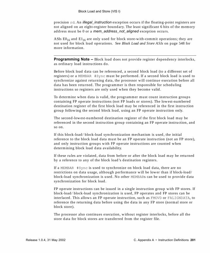
Block Load and Store (VIS I)
precision rd. An illegal_instruction exception occurs if the floating-point registers are not aligned on an eight-register boundary. The least significant 6 bits of the memory address must be 0 or a mem_address_not_aligned exception occurs.
ASIs E016 and E116 are only used for block store-with-commit operations; they are not used for block load operations. See Block Load and Store ASIs on page 548 for more information.
Programming Note – Block load does not provide register dependency interlocks, as ordinary load instructions do.
Before block load data can be referenced, a second block load (to a different set of registers) or a MEMBAR #Sync must be performed. If a second block load is used to synchronize against returning data, the processor will continue execution before all data has been returned. The programmer is then responsible for scheduling instructions so registers are only used when they become valid.
To determine when data is valid, the programmer must count instruction groups containing FP operate instructions (not FP loads or stores). The lowest-numbered destination register of the first block load may be referenced in the first instruction group following the second block load, using an FP operate instruction only.
The second-lowest-numbered destination register of the first block load may be referenced in the second instruction group containing an FP operate instruction, and so on.
If this block-load/block-load synchronization mechanism is used, the initial reference to the block load data must be an FP operate instruction (not an FP store), and only instruction groups with FP operate instructions are counted when determining block load data availability.
If these rules are violated, data from before or after the block load may be returned by a reference to any of the block load’s destination registers.
If a MEMBAR #Sync is used to synchronize on block load data, there are no restrictions on data usage, although performance will be lower than if block-load/block-load synchronization is used. No other MEMBARs can be used to provide data synchronization for block load.
FP operate instructions can be issued in a single instruction group with FP stores. If block-load/block-load synchronization is used, FP operates and FP stores can be interlaced. This allows an FP operate instruction, such as FMOVD or FALIGNDATA, to reference the returning data before using the data in any FP store (normal store or block store).
The processor also continues execution, without register interlocks, before all the store data for block stores are transferred from the register file.
Release 1.0.4, 31 May 2002 C. Appendix A • Instruction Definitions 201
Block Load and Store (VIS I)
If store source registers are overwritten before the next block store or MEMBAR #Sync instruction, then the following rule must be observed: The first register can be overwritten in the same instruction group as the block store, the second register can be overwritten in the instruction group following the block store, and so on. If this rule is violated, the block store may use the old or the new (overwritten) data.
When determining correctness for a code sample, note that JPS1 implementations may interlock more than required above. For example, there may be partial register interlocks, such as on the lowest-number register.
Code that does not meet the above constraints may appear to work on a particular implementation. However, to be portable across all SPARC JPS1 implementations, all of the above rules should be followed.
Exceptions fp_disabledPA_watchpoint (recognized on only the first 8 bytes of a transfer)VA_watchpoint (recognized on only the first 8 bytes of a transfer)illegal_instruction (misaligned rd)mem_address_not_aligneddata_access_exceptiondata_access_errorfast_data_access_MMU_missfast_data_access_protection
202 SPARC® Joint Programming Specification (JPS1): Commonality • Release 1.0.4, 31 May 2002
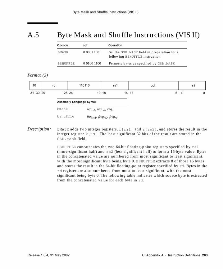
Byte Mask and Shuffle Instructions (VIS II)
A.5 Byte Mask and Shuffle Instructions (VIS II)
Format (3)
Description: BMASK adds two integer registers, r[rs1] and r[rs2], and stores the result in the integer register r[rd]. The least significant 32 bits of the result are stored in the GSR.mask field.
BSHUFFLE concatenates the two 64-bit floating-point registers specified by rs1 (more-significant half) and rs2 (less significant half) to form a 16-byte value. Bytes in the concatenated value are numbered from most significant to least significant, with the most significant byte being byte 0. BSHUFFLE extracts 8 of those 16 bytes and stores the result in the 64-bit floating-point register specified by rd. Bytes in the rd register are also numbered from most to least significant, with the most significant being byte 0. The following table indicates which source byte is extracted from the concatenated value for each byte in rd.
Opcode opf Operation
BMASK 0 0001 1001 Set the GSR.MASK field in preparation for a following BSHUFFLE instruction
BSHUFFLE 0 0100 1100 Permute bytes as specified by GSR.MASK
Assembly Language Syntax
bmask regrs1, regrs2, regrd
bshuffle fregrs1, fregrs2, fregrd
31 24 02530 29 19 18 14 13 5 4
rd10 110110 opfrs1 rs2
Release 1.0.4, 31 May 2002 C. Appendix A • Instruction Definitions 203
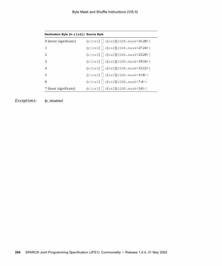
Byte Mask and Shuffle Instructions (VIS II)
Exceptions: fp_disabled
Destination Byte (in r[rd]) Source Byte
0 (most significant) (r[rs1] r[rs2])[GSR.mask<31:28>]
1 (r[rs1] r[rs2])[GSR.mask<27:24>]
2 (r[rs1] r[rs2])[GSR.mask<23:20>]
3 (r[rs1] r[rs2])[GSR.mask<19:16>]
4 (r[rs1] r[rs2])[GSR.mask<15:12>]
5 (r[rs1] r[rs2])[GSR.mask<11:8>]
6 (r[rs1] r[rs2])[GSR.mask<7:4>]
7 (least significant) (r[rs1] r[rs2])[GSR.mask<3:0>]
204 SPARC® Joint Programming Specification (JPS1): Commonality • Release 1.0.4, 31 May 2002
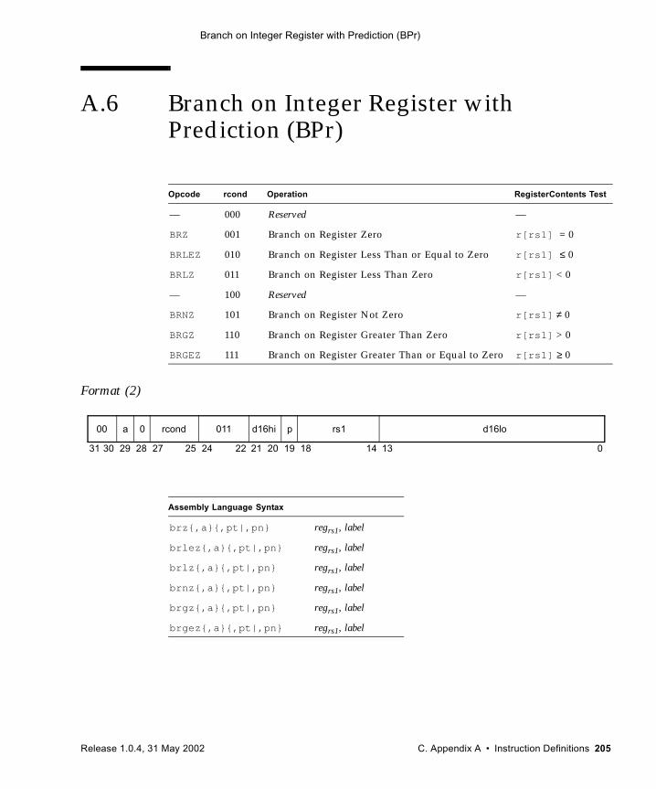
Branch on Integer Register with Prediction (BPr)
A.6 Branch on Integer Register with Prediction (BPr)
Format (2)
Opcode rcond Operation RegisterContents Test
— 000 Reserved —
BRZ 001 Branch on Register Zero r[rs1] = 0
BRLEZ 010 Branch on Register Less Than or Equal to Zero r[rs1] ≤ 0
BRLZ 011 Branch on Register Less Than Zero r[rs1] < 0
— 100 Reserved —
BRNZ 101 Branch on Register Not Zero r[rs1] ≠ 0
BRGZ 110 Branch on Register Greater Than Zero r[rs1] > 0
BRGEZ 111 Branch on Register Greater Than or Equal to Zero r[rs1] ≥ 0
Assembly Language Syntax
brz{,a}{,pt|,pn} regrs1, label
brlez{,a}{,pt|,pn} regrs1, label
brlz{,a}{,pt|,pn} regrs1, label
brnz{,a}{,pt|,pn} regrs1, label
brgz{,a}{,pt|,pn} regrs1, label
brgez{,a}{,pt|,pn} regrs1, label
31 141924 18 13 027 2530 29 28 22 21 20
00 a 0 rcond 011 d16hi p rs1 d16lo
Release 1.0.4, 31 May 2002 C. Appendix A • Instruction Definitions 205
Branch on Integer Register with Prediction (BPr)
Programming Note – To set the annul bit for BPr instructions, append “,a” to the opcode mnemonic. For example, use “brz,a %i3,label.” In the preceding table, braces signify that the “,a” is optional. To set the branch prediction bit p, append either “,pt” for predict taken or “,pn” for predict not taken to the opcode mnemonic. If neither “,pt” nor “,pn” is specified, the assembler shall default to “,pt”.
Description These instructions branch based on the contents of r[rs1]. They treat the register contents as a signed integer value.
A BPr instruction examines all 64 bits of r[rs1] according to the rcond field of the instruction, producing either a TRUE or FALSE result. If TRUE, the branch is taken; that is, the instruction causes a PC-relative, delayed control transfer to the address “PC + (4 * sign_ext(d16hi d16lo)).” If FALSE, the branch is not taken.
If the branch is taken, the delay instruction is always executed, regardless of the value of the annul bit. If the branch is not taken and the annul bit (a) is 1, the delay instruction is annulled (not executed).
The predict bit (p) gives the hardware a hint about whether the branch is expected to be taken. A 1 in the p bit indicates that the branch is expected to be taken; a 0 indicates that the branch is expected not to be taken.
Annulment, delay instructions, prediction, and delayed control transfers are described further in Chapter 6, Instructions.
Implementation Note – If this instruction is implemented by tagging each register value with an N (negative) bit and Z (zero) bit, use the table below to determine if rcond is TRUE:
Branch TestBRNZ not ZBRZ ZBRGEZ not NBRLZ NBRLEZ N or ZBRGZ not (N or Z)
Exceptions illegal_instruction (if rcond = 0002 or 1002)
206 SPARC® Joint Programming Specification (JPS1): Commonality • Release 1.0.4, 31 May 2002
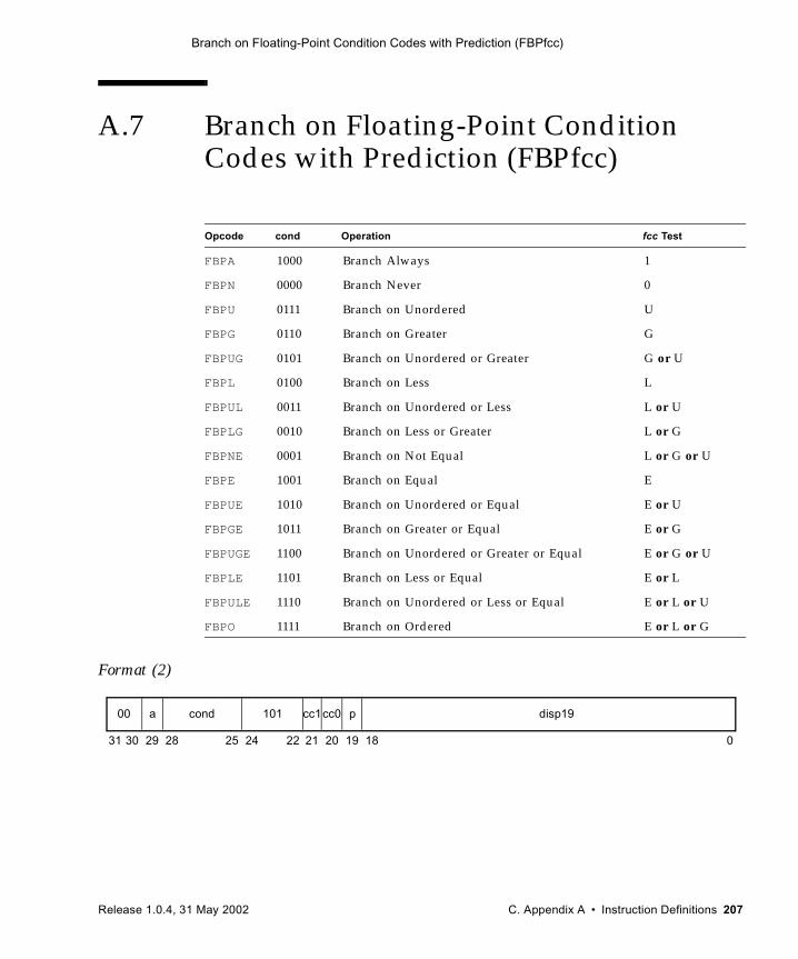
Branch on Floating-Point Condition Codes with Prediction (FBPfcc)
A.7 Branch on Floating-Point Condition Codes with Prediction (FBPfcc)
Format (2)
Opcode cond Operation fcc Test
FBPA 1000 Branch Always 1
FBPN 0000 Branch Never 0
FBPU 0111 Branch on Unordered U
FBPG 0110 Branch on Greater G
FBPUG 0101 Branch on Unordered or Greater G or U
FBPL 0100 Branch on Less L
FBPUL 0011 Branch on Unordered or Less L or U
FBPLG 0010 Branch on Less or Greater L or G
FBPNE 0001 Branch on Not Equal L or G or U
FBPE 1001 Branch on Equal E
FBPUE 1010 Branch on Unordered or Equal E or U
FBPGE 1011 Branch on Greater or Equal E or G
FBPUGE 1100 Branch on Unordered or Greater or Equal E or G or U
FBPLE 1101 Branch on Less or Equal E or L
FBPULE 1110 Branch on Unordered or Less or Equal E or L or U
FBPO 1111 Branch on Ordered E or L or G
31 1924 18 02530 29 28 22 21 20
00 a cond 101 cc1 p disp19cc0
Release 1.0.4, 31 May 2002 C. Appendix A • Instruction Definitions 207
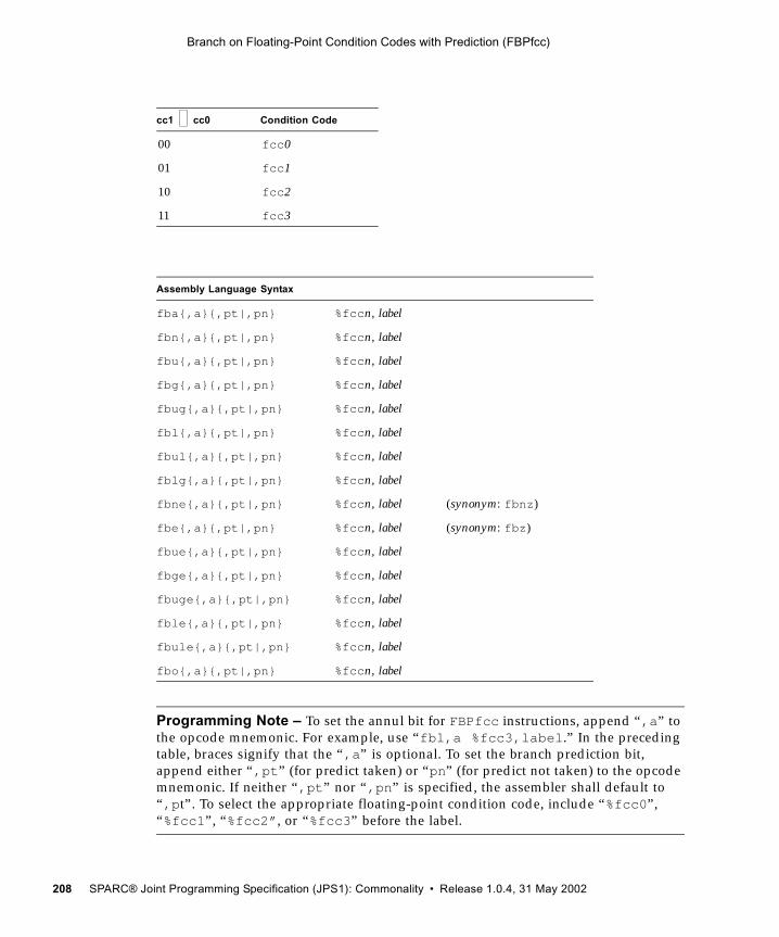
Branch on Floating-Point Condition Codes with Prediction (FBPfcc)
Programming Note – To set the annul bit for FBPfcc instructions, append “,a” to the opcode mnemonic. For example, use “fbl,a %fcc3,label.” In the preceding table, braces signify that the “,a” is optional. To set the branch prediction bit, append either “,pt” (for predict taken) or “pn” (for predict not taken) to the opcode mnemonic. If neither “,pt” nor “,pn” is specified, the assembler shall default to “,pt”. To select the appropriate floating-point condition code, include “%fcc0”, “%fcc1”, “%fcc2”, or “%fcc3” before the label.
cc1 cc0 Condition Code
00 fcc0
01 fcc1
10 fcc2
11 fcc3
Assembly Language Syntax
fba{,a}{,pt|,pn} %fccn, label
fbn{,a}{,pt|,pn} %fccn, label
fbu{,a}{,pt|,pn} %fccn, label
fbg{,a}{,pt|,pn} %fccn, label
fbug{,a}{,pt|,pn} %fccn, label
fbl{,a}{,pt|,pn} %fccn, label
fbul{,a}{,pt|,pn} %fccn, label
fblg{,a}{,pt|,pn} %fccn, label
fbne{,a}{,pt|,pn} %fccn, label (synonym: fbnz)
fbe{,a}{,pt|,pn} %fccn, label (synonym: fbz)
fbue{,a}{,pt|,pn} %fccn, label
fbge{,a}{,pt|,pn} %fccn, label
fbuge{,a}{,pt|,pn} %fccn, label
fble{,a}{,pt|,pn} %fccn, label
fbule{,a}{,pt|,pn} %fccn, label
fbo{,a}{,pt|,pn} %fccn, label
208 SPARC® Joint Programming Specification (JPS1): Commonality • Release 1.0.4, 31 May 2002
Branch on Floating-Point Condition Codes with Prediction (FBPfcc)
Description: Unconditional branches and Fcc-conditional branches are described below.
■ Unconditional branches (FBPA, FBPN) — If its annul field is 0, an FBPN (Floating-Point Branch Never with Prediction) instruction acts like a NOP. If the Branch Never’s annul field is 0, the following (delay) instruction is executed; if the annul field is 1, the following instruction is annulled (not executed). In no case does an FBPN cause a transfer of control to take place.
FBPA (Floating-Point Branch Always with Prediction) causes an unconditional PC-relative, delayed control transfer to the address “PC + (4 × sign_ext(disp19)).” If the annul field of the branch instruction is 1, the delay instruction is annulled (not executed). If the annul field is 0, the delay instruction is executed.
■ Fcc-conditional branches — Conditional FBPfcc instructions (except FBPA and FBPN) evaluate one of the four floating-point condition codes (fcc0, fcc1, fcc2, fcc3) as selected by cc0 and cc1, according to the cond field of the instruction, producing either a TRUE or FALSE result. If TRUE, the branch is taken, that is, the instruction causes a PC-relative, delayed control transfer to the address “PC + (4 × sign_ext(disp19)).” If FALSE, the branch is not taken.
If a conditional branch is taken, the delay instruction is always executed, regardless of the value of the annul field. If a conditional branch is not taken and the a (annul) field is 1, the delay instruction is annulled (not executed). Note: The annul bit has a different effect on conditional branches than it does on unconditional branches.
The predict bit (p) gives the hardware a hint about whether the branch is expected to be taken. A 1 in the p bit indicates that the branch is expected to be taken. A 0 indicates that the branch is expected not to be taken.
Annulment, delay instructions, and delayed control transfers are described further in Chapter 6, Instructions.
If FPRS.FEF = 0 or PSTATE.PEF = 0, or if an FPU is not present, an FBPfcc instruction is not executed and instead, an fp_disabled exception is generated.
Compatibility Note – Unlike SPARC V8, SPARC V9 does not require an instruction between a floating-point compare operation and a floating-point branch (FBfcc, FBPfcc).
Exceptions fp_disabled
Release 1.0.4, 31 May 2002 C. Appendix A • Instruction Definitions 209
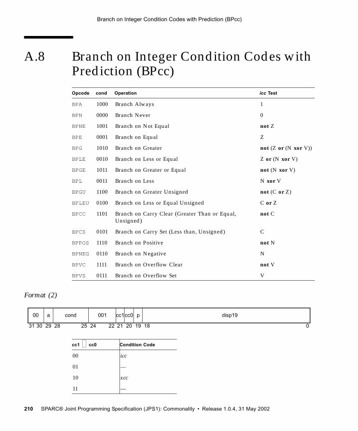
Branch on Integer Condition Codes with Prediction (BPcc)
A.8 Branch on Integer Condition Codes with Prediction (BPcc)
Format (2)
Opcode cond Operation icc Test
BPA 1000 Branch Always 1
BPN 0000 Branch Never 0
BPNE 1001 Branch on Not Equal not Z
BPE 0001 Branch on Equal Z
BPG 1010 Branch on Greater not (Z or (N xor V))
BPLE 0010 Branch on Less or Equal Z or (N xor V)
BPGE 1011 Branch on Greater or Equal not (N xor V)
BPL 0011 Branch on Less N xor V
BPGU 1100 Branch on Greater Unsigned not (C or Z)
BPLEU 0100 Branch on Less or Equal Unsigned C or Z
BPCC 1101 Branch on Carry Clear (Greater Than or Equal, Unsigned)
not C
BPCS 0101 Branch on Carry Set (Less than, Unsigned) C
BPPOS 1110 Branch on Positive not N
BPNEG 0110 Branch on Negative N
BPVC 1111 Branch on Overflow Clear not V
BPVS 0111 Branch on Overflow Set V
cc1 cc0 Condition Code
00 icc
01 —
10 xcc
11 —
31 1924 18 02530 29 28 22 21 20
00 a cond 001 cc1 p disp19cc0
210 SPARC® Joint Programming Specification (JPS1): Commonality • Release 1.0.4, 31 May 2002
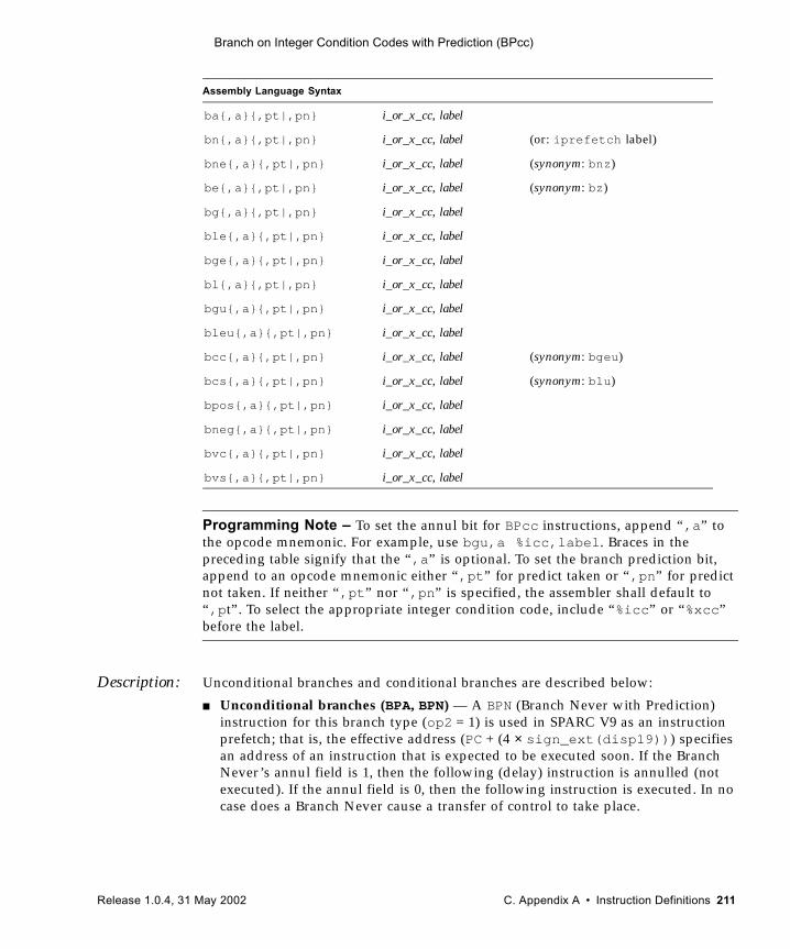
Branch on Integer Condition Codes with Prediction (BPcc)
Programming Note – To set the annul bit for BPcc instructions, append “,a” to the opcode mnemonic. For example, use bgu,a %icc,label. Braces in the preceding table signify that the “,a” is optional. To set the branch prediction bit, append to an opcode mnemonic either “,pt” for predict taken or “,pn” for predict not taken. If neither “,pt” nor “,pn” is specified, the assembler shall default to “,pt”. To select the appropriate integer condition code, include “%icc” or “%xcc” before the label.
Description: Unconditional branches and conditional branches are described below:
■ Unconditional branches (BPA, BPN) — A BPN (Branch Never with Prediction) instruction for this branch type (op2 = 1) is used in SPARC V9 as an instruction prefetch; that is, the effective address (PC + (4 × sign_ext(disp19))) specifies an address of an instruction that is expected to be executed soon. If the Branch Never’s annul field is 1, then the following (delay) instruction is annulled (not executed). If the annul field is 0, then the following instruction is executed. In no case does a Branch Never cause a transfer of control to take place.
Assembly Language Syntax
ba{,a}{,pt|,pn} i_or_x_cc, label
bn{,a}{,pt|,pn} i_or_x_cc, label (or: iprefetch label)
bne{,a}{,pt|,pn} i_or_x_cc, label (synonym: bnz)
be{,a}{,pt|,pn} i_or_x_cc, label (synonym: bz)
bg{,a}{,pt|,pn} i_or_x_cc, label
ble{,a}{,pt|,pn} i_or_x_cc, label
bge{,a}{,pt|,pn} i_or_x_cc, label
bl{,a}{,pt|,pn} i_or_x_cc, label
bgu{,a}{,pt|,pn} i_or_x_cc, label
bleu{,a}{,pt|,pn} i_or_x_cc, label
bcc{,a}{,pt|,pn} i_or_x_cc, label (synonym: bgeu)
bcs{,a}{,pt|,pn} i_or_x_cc, label (synonym: blu)
bpos{,a}{,pt|,pn} i_or_x_cc, label
bneg{,a}{,pt|,pn} i_or_x_cc, label
bvc{,a}{,pt|,pn} i_or_x_cc, label
bvs{,a}{,pt|,pn} i_or_x_cc, label
Release 1.0.4, 31 May 2002 C. Appendix A • Instruction Definitions 211
Branch on Integer Condition Codes with Prediction (BPcc)
BPA (Branch Always with Prediction) causes an unconditional PC-relative, delayed control transfer to the address “PC + (4 × sign_ext(disp19)).” If the annul field of the branch instruction is 1, then the delay instruction is annulled (not executed). If the annul field is 0, then the delay instruction is executed.
■ Conditional branches — Conditional BPcc instructions (except BPA and BPN) evaluate one of the two integer condition codes (icc or xcc), as selected by cc0 and cc1, according to the cond field of the instruction, producing either a TRUE or FALSE result. If TRUE, the branch is taken; that is, the instruction causes a PC-relative, delayed control transfer to the address “PC + (4 × sign_ext(disp19)).” If FALSE, the branch is not taken.
If a conditional branch is taken, the delay instruction is always executed regardless of the value of the annul field. If a conditional branch is not taken and the a (annul) field is 1, the delay instruction is annulled (not executed). Note: The annul bit has a different effect for conditional branches than it does for unconditional branches.
The predict bit (p) is used to give the hardware a hint about whether the branch is expected to be taken. A 1 in the p bit indicates that the branch is expected to be taken; a 0 indicates that the branch is expected not to be taken.
Annulment, delay instructions, prediction, and delayed control transfers are described further in Chapter 6, Instructions.
Exceptions illegal_instruction (cc1 cc0 = 012 or 112)
212 SPARC® Joint Programming Specification (JPS1): Commonality • Release 1.0.4, 31 May 2002
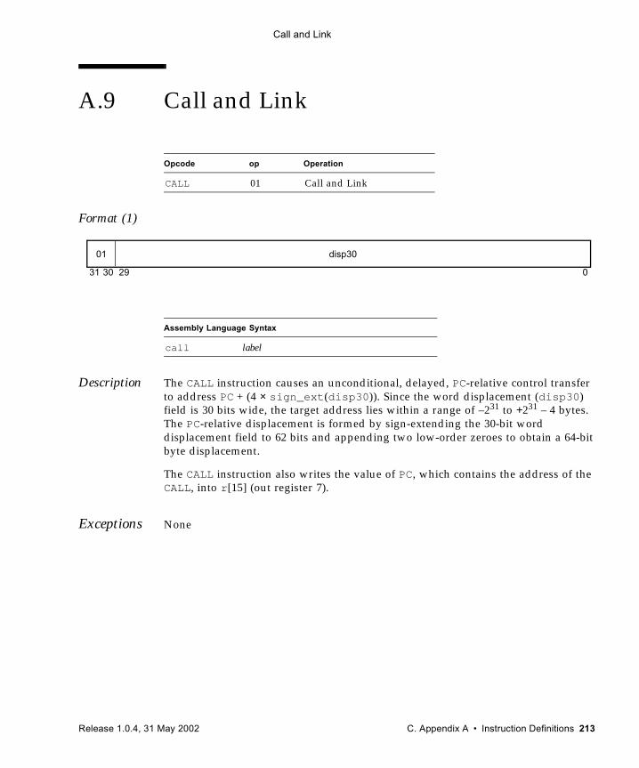
Call and Link
A.9 Call and Link
Format (1)
Description The CALL instruction causes an unconditional, delayed, PC-relative control transfer to address PC + (4 × sign_ext(disp30)). Since the word displacement (disp30) field is 30 bits wide, the target address lies within a range of –231 to +231 – 4 bytes. The PC-relative displacement is formed by sign-extending the 30-bit word displacement field to 62 bits and appending two low-order zeroes to obtain a 64-bit byte displacement.
The CALL instruction also writes the value of PC, which contains the address of the CALL, into r[15] (out register 7).
Exceptions None
Opcode op Operation
CALL 01 Call and Link
Assembly Language Syntax
call label
31 030 29
01 disp30
Release 1.0.4, 31 May 2002 C. Appendix A • Instruction Definitions 213
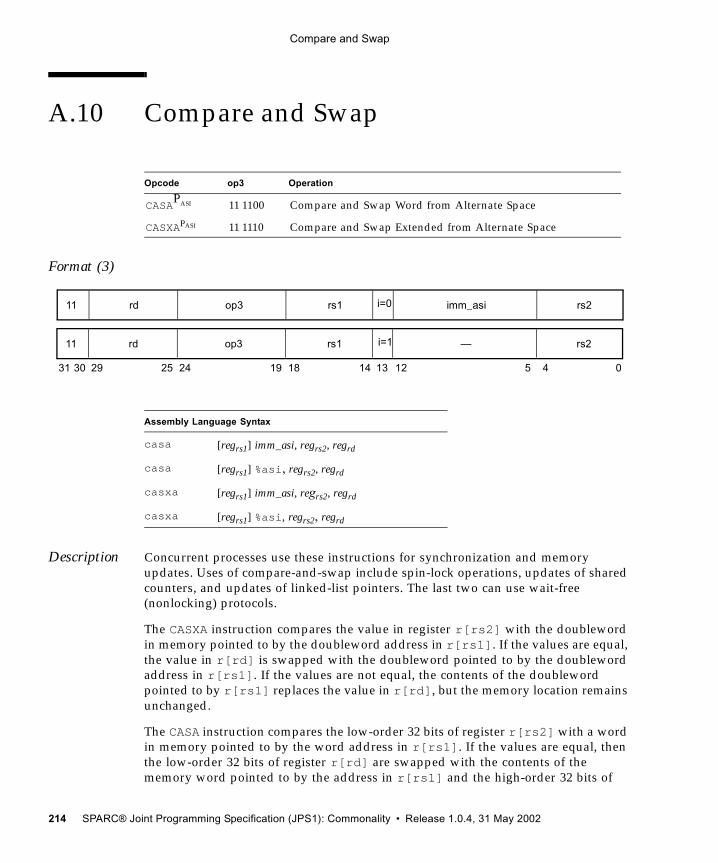
Compare and Swap
A.10 Compare and Swap
Format (3)
Description Concurrent processes use these instructions for synchronization and memory updates. Uses of compare-and-swap include spin-lock operations, updates of shared counters, and updates of linked-list pointers. The last two can use wait-free (nonlocking) protocols.
The CASXA instruction compares the value in register r[rs2] with the doubleword in memory pointed to by the doubleword address in r[rs1]. If the values are equal, the value in r[rd] is swapped with the doubleword pointed to by the doubleword address in r[rs1]. If the values are not equal, the contents of the doubleword pointed to by r[rs1] replaces the value in r[rd], but the memory location remains unchanged.
The CASA instruction compares the low-order 32 bits of register r[rs2] with a word in memory pointed to by the word address in r[rs1]. If the values are equal, then the low-order 32 bits of register r[rd] are swapped with the contents of the memory word pointed to by the address in r[rs1] and the high-order 32 bits of
Opcode op3 Operation
CASAPASI 11 1100 Compare and Swap Word from Alternate Space
CASXAPASI 11 1110 Compare and Swap Extended from Alternate Space
Assembly Language Syntax
casa [regrs1] imm_asi, regrs2, regrd
casa [regrs1] %asi, regrs2, regrd
casxa [regrs1] imm_asi, regrs2, regrd
casxa [regrs1] %asi, regrs2, regrd
31 141924 18 13 12 5 4 02530 29
11 rd op3 rs1 i=0 imm_asi rs2
11 rd op3 rs1 i=1 — rs2
214 SPARC® Joint Programming Specification (JPS1): Commonality • Release 1.0.4, 31 May 2002
Compare and Swap
register r[rd] are set to 0. If the values are not equal, the memory location remains unchanged, but the zero-extended contents of the memory word pointed to by r[rs1] replace the low-order 32 bits of r[rd] and the high-order 32 bits of register r[rd] are set to 0.
A compare-and-swap instruction comprises three operations: a load, a compare, and a swap. The overall instruction is atomic; that is, no intervening interrupts or deferred traps are recognized by the processor and no intervening update resulting from a compare-and-swap, swap, load, load-store unsigned byte, or store instruction to the doubleword containing the addressed location, or any portion of it, is performed by the memory system.
A compare-and-swap operation does not imply any memory barrier semantics. When compare-and-swap is used for synchronization, the same consideration should be given to memory barriers as if a load, store, or swap instruction were used.
A compare-and-swap operation behaves as if it performs a store, either of a new value from r[rd] or of the previous value in memory. The addressed location must be writable, even if the values in memory and r[rs2] are not equal.
If i = 0, the address space of the memory location is specified in the imm_asi field; if i = 1, the address space is specified in the ASI register.
A mem_address_not_aligned exception is generated if the address in r[rs1] is not properly aligned. CASXA and CASA cause a privileged_action exception if PSTATE.PRIV = 0 and bit 7 of the ASI is 0.
The coherence and atomicity of memory operations between processors and I/O DMA memory accesses are implementation dependent (impl. dep. #120).
Implementation Note – An implementation might cause an exception because of an error during the store memory access, even though there was no error during the load memory access.
Programming Note – Compare and Swap (CAS) and Compare and Swap Extended (CASX) synthetic instructions are available for “big endian” memory accesses. Compare and Swap Little (CASL) and Compare and Swap Extended Little (CASXL) synthetic instructions are available for “little endian” memory accesses. See Synthetic Instructions on page 484 for the syntax of these synthetic instructions.
The compare-and-swap instructions do not affect the condition codes.
Release 1.0.4, 31 May 2002 C. Appendix A • Instruction Definitions 215
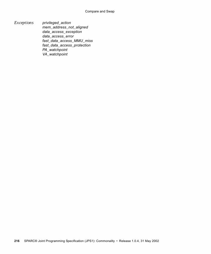
Compare and Swap
Exceptions privileged_action mem_address_not_aligneddata_access_exceptiondata_access_errorfast_data_access_MMU_missfast_data_access_protectionPA_watchpointVA_watchpoint
216 SPARC® Joint Programming Specification (JPS1): Commonality • Release 1.0.4, 31 May 2002
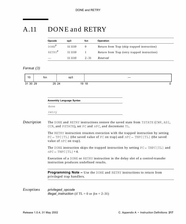
DONE and RETRY
A.11 DONE and RETRY
Format (3)
Description The DONE and RETRY instructions restore the saved state from TSTATE (CWP, ASI, CCR, and PSTATE), set PC and nPC, and decrement TL.
The RETRY instruction resumes execution with the trapped instruction by setting PC←TPC[TL] (the saved value of PC on trap) and nPC←TNPC[TL] (the saved value of nPC on trap).
The DONE instruction skips the trapped instruction by setting PC←TNPC[TL] and nPC←TNPC[TL]+4.
Execution of a DONE or RETRY instruction in the delay slot of a control-transfer instruction produces undefined results.
Programming Note – Use the DONE and RETRY instructions to return from privileged trap handlers.
Exceptions privileged_opcode illegal_instruction (if TL = 0 or fcn = 2–31)
Opcode op3 fcn Operation
DONEP 11 1110 0 Return from Trap (skip trapped instruction)
RETRYP 11 1110 1 Return from Trap (retry trapped instruction)
— 11 1110 2–31 Reserved
Assembly Language Syntax
done
retry
10 op3fcn —
31 1924 18 02530 29
Release 1.0.4, 31 May 2002 C. Appendix A • Instruction Definitions 217
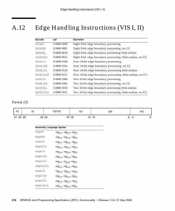
Edge Handling Instructions (VIS I, II)
A.12 Edge Handling Instructions (VIS I, II)
Format (3)
Opcode opf Operation
EDGE8 0 0000 0000 Eight 8-bit edge boundary processing
EDGE8N 0 0000 0001 Eight 8-bit edge boundary processing, no CC
EDGE8L 0 0000 0010 Eight 8-bit edge boundary processing little-endian
EDGE8LN 0 0000 0011 Eight 8-bit edge boundary processing, little-endian, no CC
EDGE16 0 0000 0100 Four 16-bit edge boundary processing
EDGE16N 0 0000 0101 Four 16-bit edge boundary processing, no CC
EDGE16L 0 0000 0110 Four 16-bit edge boundary processing little-endian
EDGE16LN 0 0000 0111 Four 16-bit edge boundary processing, little-endian, no CC
EDGE32 0 0000 1000 Two 32-bit edge boundary processing
EDGE32N 0 0000 1001 Two 32-bit edge boundary processing, no CC
EDGE32L 0 0000 1010 Two 32-bit edge boundary processing little-endian
EDGE32LN 0 0000 1011 Two 32-bit edge boundary processing, little-endian, no CC
Assembly Language Syntax
edge8 regrs1, regrs2, regrd
edge8n regrs1, regrs2, regrd
edge8l regrs1, regrs2, regrd
edge8ln regrs1, regrs2, regrd
edge16 regrs1, regrs2, regrd
edge16n regrs1, regrs2, regrd
edge16l regrs1, regrs2, regrd
edge16ln regrs1, regrs2, regrd
edge32 regrs1, regrs2, regrd
edge32n regrs1, regrs2, regrd
edge32l regrs1, regrs2, regrd
edge32ln regrs1, regrs2, regrd
31 24 02530 29 19 18 14 13 5 4
rd10 110110 opfrs1 rs2
218 SPARC® Joint Programming Specification (JPS1): Commonality • Release 1.0.4, 31 May 2002
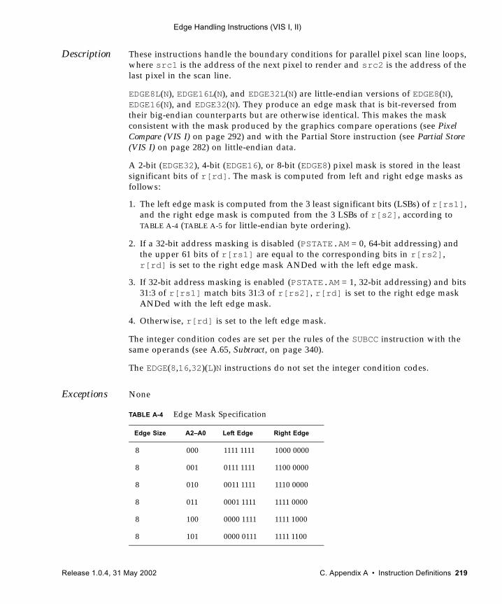
Edge Handling Instructions (VIS I, II)
Description These instructions handle the boundary conditions for parallel pixel scan line loops, where src1 is the address of the next pixel to render and src2 is the address of the last pixel in the scan line.
EDGE8L(N), EDGE16L(N), and EDGE32L(N) are little-endian versions of EDGE8(N), EDGE16(N), and EDGE32(N). They produce an edge mask that is bit-reversed from their big-endian counterparts but are otherwise identical. This makes the mask consistent with the mask produced by the graphics compare operations (see Pixel Compare (VIS I) on page 292) and with the Partial Store instruction (see Partial Store (VIS I) on page 282) on little-endian data.
A 2-bit (EDGE32), 4-bit (EDGE16), or 8-bit (EDGE8) pixel mask is stored in the least significant bits of r[rd]. The mask is computed from left and right edge masks as follows:
1. The left edge mask is computed from the 3 least significant bits (LSBs) of r[rs1], and the right edge mask is computed from the 3 LSBs of r[s2], according to TABLE A-4 (TABLE A-5 for little-endian byte ordering).
2. If a 32-bit address masking is disabled (PSTATE.AM = 0, 64-bit addressing) and the upper 61 bits of r[rs1] are equal to the corresponding bits in r[rs2], r[rd] is set to the right edge mask ANDed with the left edge mask.
3. If 32-bit address masking is enabled (PSTATE.AM = 1, 32-bit addressing) and bits 31:3 of r[rs1] match bits 31:3 of r[rs2], r[rd] is set to the right edge mask ANDed with the left edge mask.
4. Otherwise, r[rd] is set to the left edge mask.
The integer condition codes are set per the rules of the SUBCC instruction with the same operands (see A.65, Subtract, on page 340).
The EDGE(8,16,32)(L)N instructions do not set the integer condition codes.
Exceptions None
TABLE A-4 Edge Mask Specification
Edge Size A2–A0 Left Edge Right Edge
8 000 1111 1111 1000 0000
8 001 0111 1111 1100 0000
8 010 0011 1111 1110 0000
8 011 0001 1111 1111 0000
8 100 0000 1111 1111 1000
8 101 0000 0111 1111 1100
Release 1.0.4, 31 May 2002 C. Appendix A • Instruction Definitions 219
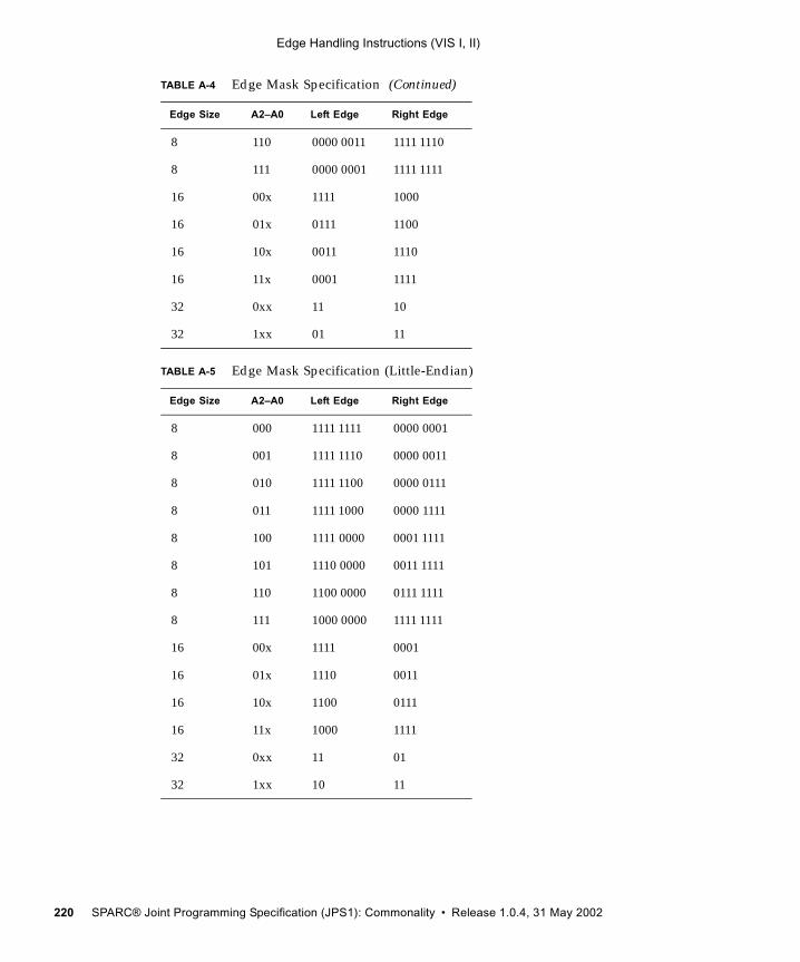
Edge Handling Instructions (VIS I, II)
8 110 0000 0011 1111 1110
8 111 0000 0001 1111 1111
16 00x 1111 1000
16 01x 0111 1100
16 10x 0011 1110
16 11x 0001 1111
32 0xx 11 10
32 1xx 01 11
TABLE A-5 Edge Mask Specification (Little-Endian)
Edge Size A2–A0 Left Edge Right Edge
8 000 1111 1111 0000 0001
8 001 1111 1110 0000 0011
8 010 1111 1100 0000 0111
8 011 1111 1000 0000 1111
8 100 1111 0000 0001 1111
8 101 1110 0000 0011 1111
8 110 1100 0000 0111 1111
8 111 1000 0000 1111 1111
16 00x 1111 0001
16 01x 1110 0011
16 10x 1100 0111
16 11x 1000 1111
32 0xx 11 01
32 1xx 10 11
TABLE A-4 Edge Mask Specification (Continued)
Edge Size A2–A0 Left Edge Right Edge
220 SPARC® Joint Programming Specification (JPS1): Commonality • Release 1.0.4, 31 May 2002
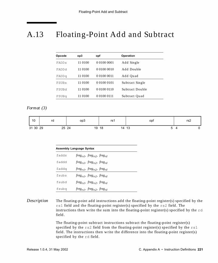
Floating-Point Add and Subtract
A.13 Floating-Point Add and Subtract
Format (3)
Description The floating-point add instructions add the floating-point register(s) specified by the rs1 field and the floating-point register(s) specified by the rs2 field. The instructions then write the sum into the floating-point register(s) specified by the rd field.
The floating-point subtract instructions subtract the floating-point register(s) specified by the rs2 field from the floating-point register(s) specified by the rs1 field. The instructions then write the difference into the floating-point register(s) specified by the rd field.
Opcode op3 opf Operation
FADDs 11 0100 0 0100 0001 Add Single
FADDd 11 0100 0 0100 0010 Add Double
FADDq 11 0100 0 0100 0011 Add Quad
FSUBs 11 0100 0 0100 0101 Subtract Single
FSUBd 11 0100 0 0100 0110 Subtract Double
FSUBq 11 0100 0 0100 0111 Subtract Quad
Assembly Language Syntax
fadds fregrs1, fregrs2, fregrd
faddd fregrs1, fregrs2, fregrd
faddq fregrs1, fregrs2, fregrd
fsubs fregrs1, fregrs2, fregrd
fsubd fregrs1, fregrs2, fregrd
fsubq fregrs1, fregrs2, fregrd
10 op3 rs2rd rs1
31 141924 18 13 02530 29 4
opf
5
Release 1.0.4, 31 May 2002 C. Appendix A • Instruction Definitions 221
Floating-Point Add and Subtract
Rounding is performed as specified by the FSR.RD field.
Notes – 1) SPARC JPS1 processors do not implement in hardware the instructions that refer to a quad floating-point register. Execution of such an instruction generates fp_exception_other (with ftt = unimplemented_FPop), which causes a trap. Supervisor software then emulates these instructions.
2) For FADDs, FADDd, FSUBs, FSUBd, an fp_exception_other with ftt = unfinished_FPop can occur if the add/subtract operation detects certain unusual conditions. See TABLE 5-9 on page 61 for details.
Exceptions fp_disabled fp_exception_ieee_754 (OF, UF, NX, NV) fp_exception_other (ftt = unimplemented_FPop (FADDq and FSUBq only))fp_exception_other (ftt = unifinished_FPop (FADDs, FADDd, FSUBs, FSUBd only))
222 SPARC® Joint Programming Specification (JPS1): Commonality • Release 1.0.4, 31 May 2002
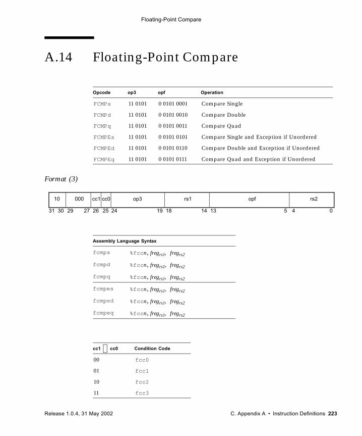
Floating-Point Compare
A.14 Floating-Point Compare
Format (3)
Opcode op3 opf Operation
FCMPs 11 0101 0 0101 0001 Compare Single
FCMPd 11 0101 0 0101 0010 Compare Double
FCMPq 11 0101 0 0101 0011 Compare Quad
FCMPEs 11 0101 0 0101 0101 Compare Single and Exception if Unordered
FCMPEd 11 0101 0 0101 0110 Compare Double and Exception if Unordered
FCMPEq 11 0101 0 0101 0111 Compare Quad and Exception if Unordered
Assembly Language Syntax
fcmps %fccn, fregrs1, fregrs2
fcmpd %fccn, fregrs1, fregrs2
fcmpq %fccn, fregrs1, fregrs2
fcmpes %fccn, fregrs1, fregrs2
fcmped %fccn, fregrs1, fregrs2
fcmpeq %fccn, fregrs1, fregrs2
cc1 cc0 Condition Code
00 fcc0
01 fcc1
10 fcc2
11 fcc3
10 op3 rs2000 rs1
31 141924 18 13 02530 29 4
opf
52627
cc1 cc0
Release 1.0.4, 31 May 2002 C. Appendix A • Instruction Definitions 223
Floating-Point Compare
Description These instructions compare the floating-point register(s) specified by the rs1 field with the floating-point register(s) specified by the rs2 field, and set the selected floating-point condition code (fccn) as shown below.
The “?” in the preceding table means that the comparison is unordered. The unordered condition occurs when one or both of the operands to the compare is a signalling or quiet NaN.
The “compare and cause exception if unordered” (FCMPEs, FCMPEd, and FCMPEq) instructions cause an invalid (NV) exception if either operand is a NaN.
FCMP causes an invalid (NV) exception if either operand is a signalling NaN.
Compatibility Note – Unlike SPARC V8, SPARC V9 does not require an instruction between a floating-point compare operation and a floating-point branch (FBfcc, FBPfcc).
SPARC V8 floating-point compare instructions are required to have a 0 in the r[rd] field. In SPARC V9, bits 26 and 25 of the r[rd] field specify the floating-point condition code to be set. Legal SPARC V8 code will work on SPARC V9 because the zeroes in the r[rd] field are interpreted as fcc0 and the FBfcc instruction branches according to fcc0.
Note – SPARC V9 JPS1 instructions do not implement in hardware the instructions that refer to a quad floating-point register. Execution of such an instruction generates fp_exception_other (with ftt = unimplemented_FPop), which causes a trap. Supervisor software then emulates these instructions.
Exceptions fp_disabledfp_exception_ieee_754 (NV)fp_exception_other (ftt = unimplemented_FPop (FCMPq, FCMPEq only))
fcc value Relation
0 fregrs1 = fregrs2
1 fregrs1 < fregrs2
2 fregrs1 > fregrs2
3 fregrs1 ? fregrs2 (unordered)
224 SPARC® Joint Programming Specification (JPS1): Commonality • Release 1.0.4, 31 May 2002
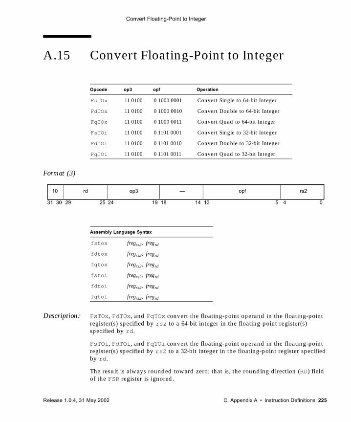
Convert Floating-Point to Integer
A.15 Convert Floating-Point to Integer
Format (3)
Description: FsTOx, FdTOx, and FqTOx convert the floating-point operand in the floating-point register(s) specified by rs2 to a 64-bit integer in the floating-point register(s) specified by rd.
FsTOi, FdTOi, and FqTOi convert the floating-point operand in the floating-point register(s) specified by rs2 to a 32-bit integer in the floating-point register specified by rd.
The result is always rounded toward zero; that is, the rounding direction (RD) field of the FSR register is ignored.
Opcode op3 opf Operation
FsTOx 11 0100 0 1000 0001 Convert Single to 64-bit Integer
FdTOx 11 0100 0 1000 0010 Convert Double to 64-bit Integer
FqTOx 11 0100 0 1000 0011 Convert Quad to 64-bit Integer
FsTOi 11 0100 0 1101 0001 Convert Single to 32-bit Integer
FdTOi 11 0100 0 1101 0010 Convert Double to 32-bit Integer
FqTOi 11 0100 0 1101 0011 Convert Quad to 32-bit Integer
Assembly Language Syntax
fstox fregrs2, fregrd
fdtox fregrs2, fregrd
fqtox fregrs2, fregrd
fstoi fregrs2, fregrd
fdtoi fregrs2, fregrd
fqtoi fregrs2, fregrd
10 op3 rs2rd —
31 141924 18 13 02530 29 4
opf
5
Release 1.0.4, 31 May 2002 C. Appendix A • Instruction Definitions 225
Convert Floating-Point to Integer
If the floating-point operand’s value is too large to be converted to an integer of the specified size or is a NaN or infinity, then an fp_exception_ieee_754 “invalid” exception occurs. The value written into the floating-point register(s) specified by rd in these cases is as defined in Integer Overflow Definition on page 396.
Note – SPARC V9 JPS1 instructions do not implement in hardware the instructions that refer to a quad floating-point register. Execution of such an instruction generates fp_exception_other (with ftt = unimplemented_FPop), which causes a trap. Supervisor software then emulates these instructions.
Exceptions fp_disabled fp_exception_ieee_754 (NV, NX) fp_exception_other (ftt = unimplemented_FPop (FqTOi, FqTOx only))
226 SPARC® Joint Programming Specification (JPS1): Commonality • Release 1.0.4, 31 May 2002
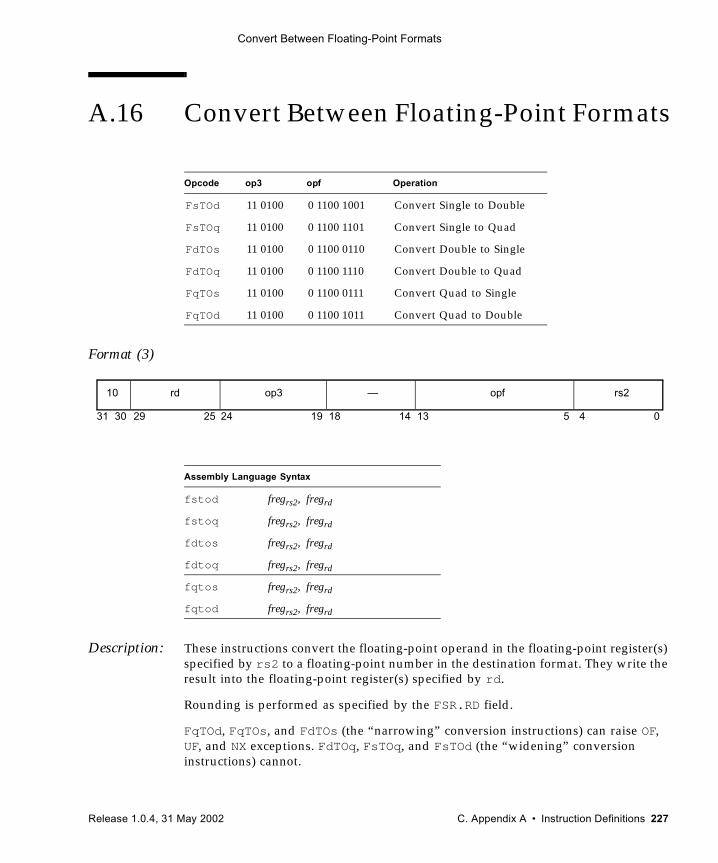
Convert Between Floating-Point Formats
A.16 Convert Between Floating-Point Formats
Format (3)
Description: These instructions convert the floating-point operand in the floating-point register(s) specified by rs2 to a floating-point number in the destination format. They write the result into the floating-point register(s) specified by rd.
Rounding is performed as specified by the FSR.RD field.
FqTOd, FqTOs, and FdTOs (the “narrowing” conversion instructions) can raise OF, UF, and NX exceptions. FdTOq, FsTOq, and FsTOd (the “widening” conversion instructions) cannot.
Opcode op3 opf Operation
FsTOd 11 0100 0 1100 1001 Convert Single to Double
FsTOq 11 0100 0 1100 1101 Convert Single to Quad
FdTOs 11 0100 0 1100 0110 Convert Double to Single
FdTOq 11 0100 0 1100 1110 Convert Double to Quad
FqTOs 11 0100 0 1100 0111 Convert Quad to Single
FqTOd 11 0100 0 1100 1011 Convert Quad to Double
Assembly Language Syntax
fstod fregrs2, fregrd
fstoq fregrs2, fregrd
fdtos fregrs2, fregrd
fdtoq fregrs2, fregrd
fqtos fregrs2, fregrd
fqtod fregrs2, fregrd
10 op3 rs2rd —
31 141924 18 13 02530 29 4
opf
5
Release 1.0.4, 31 May 2002 C. Appendix A • Instruction Definitions 227
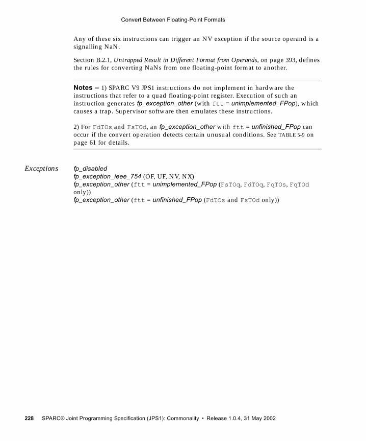
Convert Between Floating-Point Formats
Any of these six instructions can trigger an NV exception if the source operand is a signalling NaN.
Section B.2.1, Untrapped Result in Different Format from Operands, on page 393, defines the rules for converting NaNs from one floating-point format to another.
Notes – 1) SPARC V9 JPS1 instructions do not implement in hardware the instructions that refer to a quad floating-point register. Execution of such an instruction generates fp_exception_other (with ftt = unimplemented_FPop), which causes a trap. Supervisor software then emulates these instructions.
2) For FdTOs and FsTOd, an fp_exception_other with ftt = unfinished_FPop can occur if the convert operation detects certain unusual conditions. See TABLE 5-9 on page 61 for details.
Exceptions fp_disabled fp_exception_ieee_754 (OF, UF, NV, NX) fp_exception_other (ftt = unimplemented_FPop (FsTOq, FdTOq, FqTOs, FqTOd only))fp_exception_other (ftt = unfinished_FPop (FdTOs and FsTOd only))
228 SPARC® Joint Programming Specification (JPS1): Commonality • Release 1.0.4, 31 May 2002
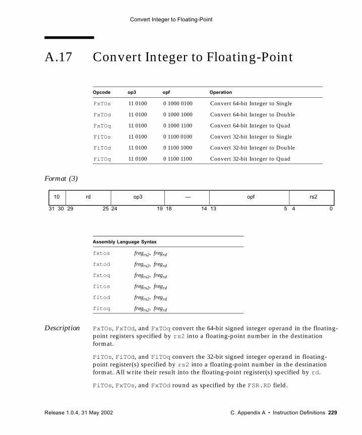
Convert Integer to Floating-Point
A.17 Convert Integer to Floating-Point
Format (3)
Description FxTOs, FxTOd, and FxTOq convert the 64-bit signed integer operand in the floating-point registers specified by rs2 into a floating-point number in the destination format.
FiTOs, FiTOd, and FiTOq convert the 32-bit signed integer operand in floating-point register(s) specified by rs2 into a floating-point number in the destination format. All write their result into the floating-point register(s) specified by rd.
FiTOs, FxTOs, and FxTOd round as specified by the FSR.RD field.
Opcode op3 opf Operation
FxTOs 11 0100 0 1000 0100 Convert 64-bit Integer to Single
FxTOd 11 0100 0 1000 1000 Convert 64-bit Integer to Double
FxTOq 11 0100 0 1000 1100 Convert 64-bit Integer to Quad
FiTOs 11 0100 0 1100 0100 Convert 32-bit Integer to Single
FiTOd 11 0100 0 1100 1000 Convert 32-bit Integer to Double
FiTOq 11 0100 0 1100 1100 Convert 32-bit Integer to Quad
Assembly Language Syntax
fxtos fregrs2, fregrd
fxtod fregrs2, fregrd
fxtoq fregrs2, fregrd
fitos fregrs2, fregrd
fitod fregrs2, fregrd
fitoq fregrs2, fregrd
10 op3 rs2rd —
31 141924 18 13 02530 29 4
opf
5
Release 1.0.4, 31 May 2002 C. Appendix A • Instruction Definitions 229
Convert Integer to Floating-Point
Note – SPARC V9 JPS1 instructions do not implement in hardware the instructions that refer to a quad floating-point register. Execution of such an instruction generates fp_exception_other (with ftt = unimplemented_FPop), which causes a trap. Supervisor software then emulates these instructions.
Exceptions fp_disabled fp_exception_ieee_754 (NX (FiTOs, FxTOs, FxTOd only)) fp_exception_other (ftt = unimplemented_FPop (FiTOq, FxTOq only))
230 SPARC® Joint Programming Specification (JPS1): Commonality • Release 1.0.4, 31 May 2002
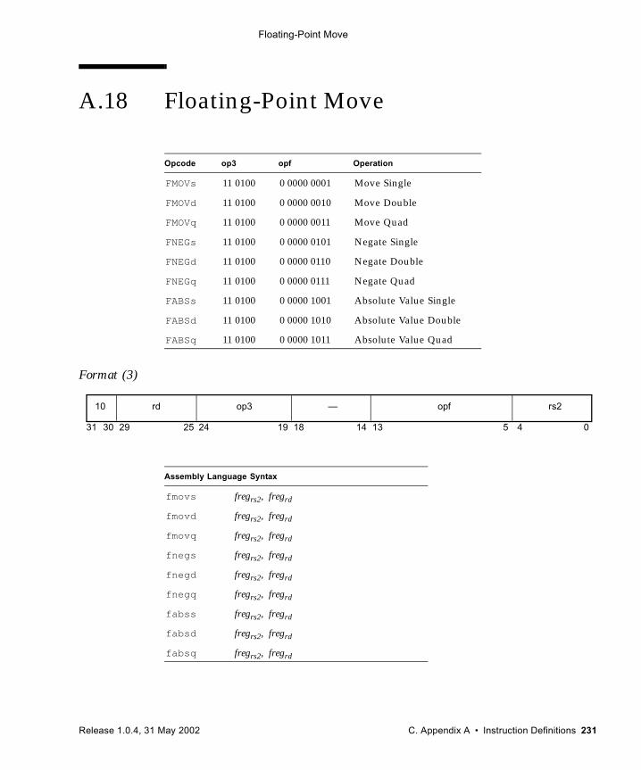
Floating-Point Move
A.18 Floating-Point Move
Format (3)
Opcode op3 opf Operation
FMOVs 11 0100 0 0000 0001 Move Single
FMOVd 11 0100 0 0000 0010 Move Double
FMOVq 11 0100 0 0000 0011 Move Quad
FNEGs 11 0100 0 0000 0101 Negate Single
FNEGd 11 0100 0 0000 0110 Negate Double
FNEGq 11 0100 0 0000 0111 Negate Quad
FABSs 11 0100 0 0000 1001 Absolute Value Single
FABSd 11 0100 0 0000 1010 Absolute Value Double
FABSq 11 0100 0 0000 1011 Absolute Value Quad
Assembly Language Syntax
fmovs fregrs2, fregrd
fmovd fregrs2, fregrd
fmovq fregrs2, fregrd
fnegs fregrs2, fregrd
fnegd fregrs2, fregrd
fnegq fregrs2, fregrd
fabss fregrs2, fregrd
fabsd fregrs2, fregrd
fabsq fregrs2, fregrd
10 op3 rs2rd —
31 141924 18 13 02530 29 4
opf
5
Release 1.0.4, 31 May 2002 C. Appendix A • Instruction Definitions 231
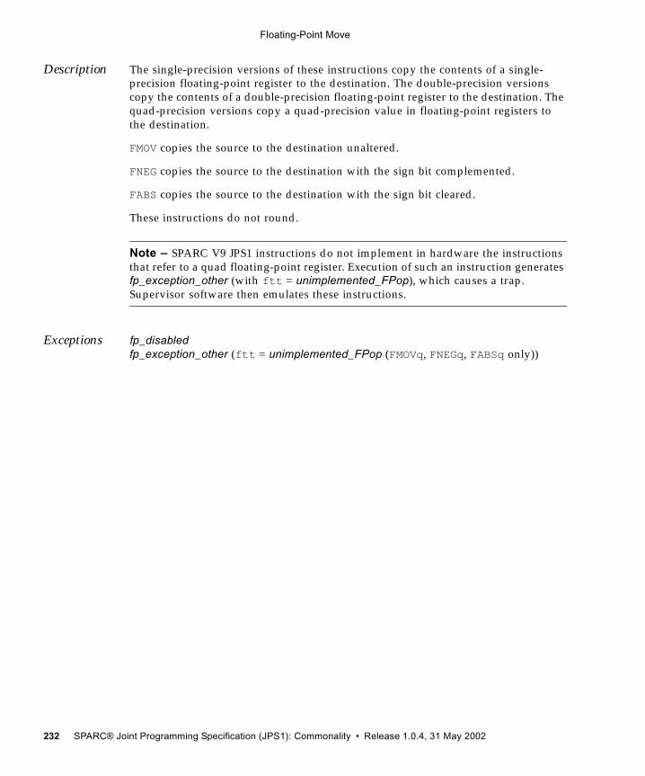
Floating-Point Move
Description The single-precision versions of these instructions copy the contents of a single-precision floating-point register to the destination. The double-precision versions copy the contents of a double-precision floating-point register to the destination. The quad-precision versions copy a quad-precision value in floating-point registers to the destination.
FMOV copies the source to the destination unaltered.
FNEG copies the source to the destination with the sign bit complemented.
FABS copies the source to the destination with the sign bit cleared.
These instructions do not round.
Note – SPARC V9 JPS1 instructions do not implement in hardware the instructions that refer to a quad floating-point register. Execution of such an instruction generates fp_exception_other (with ftt = unimplemented_FPop), which causes a trap. Supervisor software then emulates these instructions.
Exceptions fp_disabled fp_exception_other (ftt = unimplemented_FPop (FMOVq, FNEGq, FABSq only))
232 SPARC® Joint Programming Specification (JPS1): Commonality • Release 1.0.4, 31 May 2002
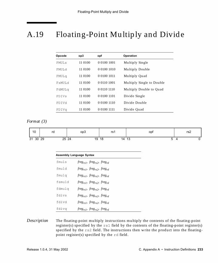
Floating-Point Multiply and Divide
A.19 Floating-Point Multiply and Divide
Format (3)
Description The floating-point multiply instructions multiply the contents of the floating-point register(s) specified by the rs1 field by the contents of the floating-point register(s) specified by the rs2 field. The instructions then write the product into the floating-point register(s) specified by the rd field.
Opcode op3 opf Operation
FMULs 11 0100 0 0100 1001 Multiply Single
FMULd 11 0100 0 0100 1010 Multiply Double
FMULq 11 0100 0 0100 1011 Multiply Quad
FsMULd 11 0100 0 0110 1001 Multiply Single to Double
FdMULq 11 0100 0 0110 1110 Multiply Double to Quad
FDIVs 11 0100 0 0100 1101 Divide Single
FDIVd 11 0100 0 0100 1110 Divide Double
FDIVq 11 0100 0 0100 1111 Divide Quad
Assembly Language Syntax
fmuls fregrs1, fregrs2, fregrd
fmuld fregrs1, fregrs2, fregrd
fmulq fregrs1, fregrs2, fregrd
fsmuld fregrs1, fregrs2, fregrd
fdmulq fregrs1, fregrs2, fregrd
fdivs fregrs1, fregrs2, fregrd
fdivd fregrs1, fregrs2, fregrd
fdivq fregrs1, fregrs2, fregrd
10 op3 rs2rd rs1
31 141924 18 13 02530 29 4
opf
5
Release 1.0.4, 31 May 2002 C. Appendix A • Instruction Definitions 233
Floating-Point Multiply and Divide
The FsMULd instruction provides the exact double-precision product of two single-precision operands, without underflow, overflow, or rounding error. Similarly, FdMULq provides the exact quad-precision product of two double-precision operands.
The floating-point divide instructions divide the contents of the floating-point register(s) specified by the rs1 field by the contents of the floating-point register(s) specified by the rs2 field. The instructions then write the quotient into the floating-point register(s) specified by the rd field.
Rounding is performed as specified by the FSR.RD field.
Notes – 1) SPARC V9 JPS1 instructions do not implement in hardware the instructions that refer to a quad floating-point register. Execution of such an instruction generates fp_exception_other (with ftt = unimplemented_FPop), which causes a trap. Supervisor software then emulates these instructions.
2) For FDIVs and FDIVd, an fp_exception_other with ftt = unfinished_FPop can occur if the divide unit detects certain unusual conditions. See TABLE 5-9 on page 61 for details.
Exceptions fp_disabled fp_exception_ieee_754 (OF, UF, DZ (FDIV only), NV, NX) fp_exception_other (ftt = unimplemented_FPop (FMULq, FdMULq, FDIVq) fp_exception_other (ftt = unifinished_FPop (FMULs, FMULd, FSMULd, FDIVs, FDIV))
234 SPARC® Joint Programming Specification (JPS1): Commonality • Release 1.0.4, 31 May 2002
Floating-Point Square Root
A.20 Floating-Point Square Root
Format (3)
Description These SPARC V9 instructions generate the square root of the floating-point operand in the floating-point register(s) specified by the rs2 field and place the result in the destination floating-point register(s) specified by the rd field. Rounding is performed as specified by the FSR.RD field.
Note – SPARC V9 JPS1 instructions do not implement in hardware the instructions that refer to a quad floating-point register. Execution of such an instruction generates fp_exception_other (with ftt = unimplemented_FPop), which causes a trap. Supervisor software then emulates these instructions.
For FSQRTs and FSQRTd an fp_exception_other (with ftt = unfinished_FPop) can occur if the operand to the square root is positive denormalized. See FSR_floating-point_trap_type (ftt) on page 59 for additional details.
Exceptions fp_disabledfp_exception_ieee_754 (IEEE_754_exception (NV, NX))fp_exception_other (unimplemented_FPop) (Quad forms)fp_exception_other (unfinished_FPop) (FSQRTs, FSQRTd)
Opcode op3 opf Operation
FSQRTs 11 0100 0 0010 1001 Square Root Single
FSQRTd 11 0100 0 0010 1010 Square Root Double
FSQRTq 11 0100 0 0010 1011 Square Root Quad
Assembly Language Syntax
fsqrts fregrs2, fregrd
fsqrtd fregrs2, fregrd
fsqrtq fregrs2, fregrd
10 op3 rs2rd —
31 141924 18 13 02530 29 4
opf
5
Release 1.0.4, 31 May 2002 C. Appendix A • Instruction Definitions 235
Flush Instruction Memory
A.21 Flush Instruction Memory
Format (3)
Description FLUSH ensures that the doubleword specified as the effective address is consistent across any local caches and, in a multiprocessor system, will eventually become consistent everywhere.
In the following discussion PFLUSH refers to the processor that executed the FLUSH instruction.
FLUSH ensures that instruction fetches from the specified effective address by PFLUSH appear to execute after any loads, stores, and atomic load-stores to that address issued by PFLUSH prior to the FLUSH. In a multiprocessor system, FLUSH also ensures that these values will eventually become visible to the instruction fetches of all other processors. FLUSH behaves as if it were a store with respect to MEMBAR-induced orderings. See A.35, Memory Barrier.
The effective address operand for the FLUSH instruction is “r[rs1] + r[rs2]” if i = 0, or “r[rs1] + sign_ext(simm13)” if i = 1. The least significant two address bits of the effective address are unused and should be supplied as zeroes by software. Bit 2 of the address is ignored because FLUSH operates on at least a doubleword.
Opcode op3 Operation
FLUSH 11 1011 Flush Instruction Memory
Assembly Language Syntax
flush address
31 24 02530 29 19 18
—10 op3 —
14 13 12 5 4
rs1 rs2i=0
10 op3 rs1 simm13i=1—
236 SPARC® Joint Programming Specification (JPS1): Commonality • Release 1.0.4, 31 May 2002
Flush Instruction Memory
Programming Notes –
1. Typically, FLUSH is used in self-modifying code. See H.1.6, Self-Modifying Code, for information about use of the FLUSH instruction in portable self-modifying code. The use of self-modifying code is discouraged.
2. The order in which memory is modified can be controlled by means of FLUSH and MEMBAR instructions interspersed appropriately between stores and atomic load-stores. FLUSH is needed only between a store and a subsequent instruction fetch from the modified location. When multiple processes may concurrently modify live (that is, potentially executing) code, the programmer must ensure that the order of update maintains the program in a semantically correct form at all times.
3. The memory model guarantees in a uniprocessor that data loads observe the results of the most recent store, even if there is no intervening FLUSH.
4. FLUSH may be time consuming.
5. In a multiprocessor system, the time it takes for a FLUSH to take effect is implementation dependent. No mechanism is provided to ensure or test completion.
6. Because FLUSH is designed to act on a doubleword and because, on some implementations, FLUSH may trap to system software, system software should provide a user-callable service routine for flushing arbitrarily sized regions of memory. On some implementations, this routine would issue a series of FLUSH instructions; on others, it might issue a single trap to system software that would then flush the entire region.
IMPL. DEP. #42: If FLUSH is not implemented in hardware, it causes an illegal_instruction exception and the function of FLUSH is performed by system software. Whether FLUSH traps is implementation dependent.
Implementation Note – The effect of a FLUSH instruction as observed from the processor on which FLUSH executes is immediate. Other processors in a multiprocessor system eventually will see the effect of the FLUSH, but the latency is implementation dependent.
On a SPARC JPS1 processor:
■ A FLUSH instruction flushes the processor pipeline and synchronizes the processor.
■ Coherency between instruction and data memories is maintained by hardware; therefore, a JPS1 implementation may ignore the address in a FLUSH instruction’s operands. However, for portability across all SPARC V9 implementations, software must supply the target effective address in FLUSH instructions.
Exceptions None
Release 1.0.4, 31 May 2002 C. Appendix A • Instruction Definitions 237
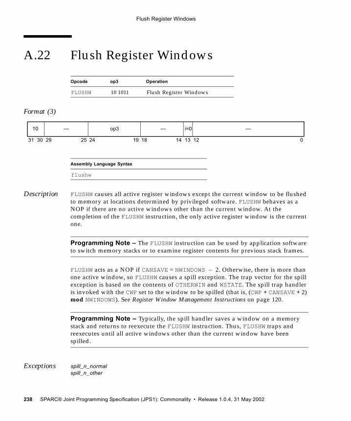
Flush Register Windows
A.22 Flush Register Windows
Format (3)
Description FLUSHW causes all active register windows except the current window to be flushed to memory at locations determined by privileged software. FLUSHW behaves as a NOP if there are no active windows other than the current window. At the completion of the FLUSHW instruction, the only active register window is the current one.
Programming Note – The FLUSHW instruction can be used by application software to switch memory stacks or to examine register contents for previous stack frames.
FLUSHW acts as a NOP if CANSAVE = NWINDOWS – 2. Otherwise, there is more than one active window, so FLUSHW causes a spill exception. The trap vector for the spill exception is based on the contents of OTHERWIN and WSTATE. The spill trap handler is invoked with the CWP set to the window to be spilled (that is, (CWP + CANSAVE + 2) mod NWINDOWS). See Register Window Management Instructions on page 120.
Programming Note – Typically, the spill handler saves a window on a memory stack and returns to reexecute the FLUSHW instruction. Thus, FLUSHW traps and reexecutes until all active windows other than the current window have been spilled.
Exceptions spill_n_normalspill_n_other
Opcode op3 Operation
FLUSHW 10 1011 Flush Register Windows
Assembly Language Syntax
flushw
31 24 02530 29 19 18
—10 op3 —
14 13 12
— i=0
238 SPARC® Joint Programming Specification (JPS1): Commonality • Release 1.0.4, 31 May 2002
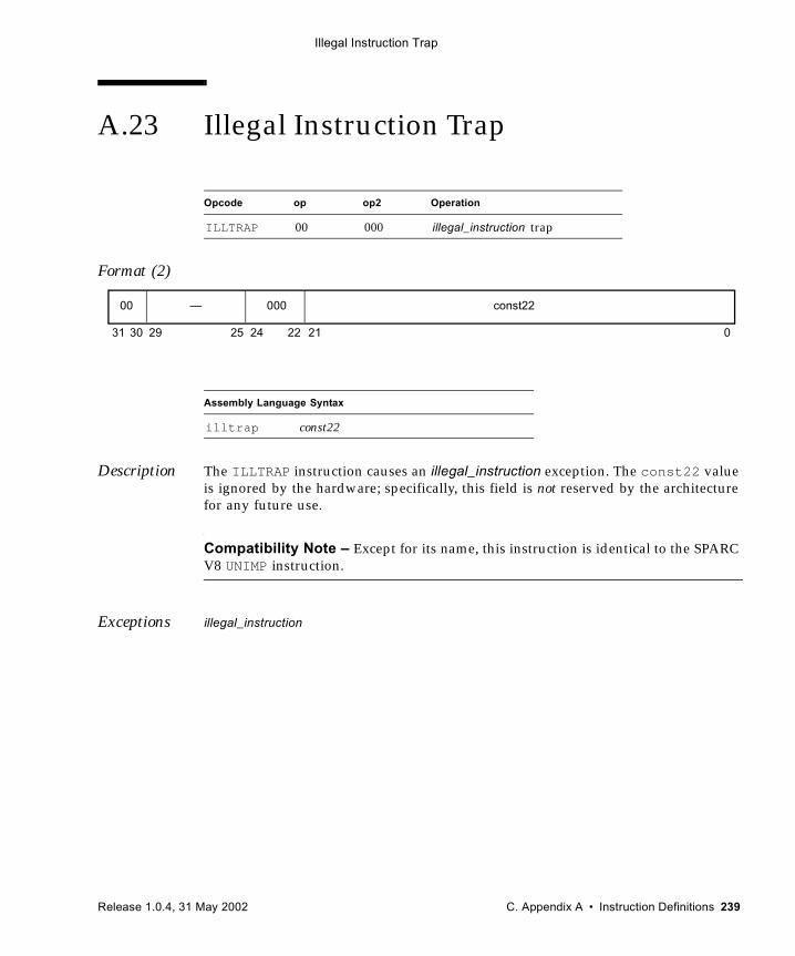
Illegal Instruction Trap
A.23 Illegal Instruction Trap
Format (2)
Description The ILLTRAP instruction causes an illegal_instruction exception. The const22 value is ignored by the hardware; specifically, this field is not reserved by the architecture for any future use.
Compatibility Note – Except for its name, this instruction is identical to the SPARC V8 UNIMP instruction.
Exceptions illegal_instruction
Opcode op op2 Operation
ILLTRAP 00 000 illegal_instruction trap
Assembly Language Syntax
illtrap const22
00 000 const22—
31 2124 02530 29 22
Release 1.0.4, 31 May 2002 C. Appendix A • Instruction Definitions 239
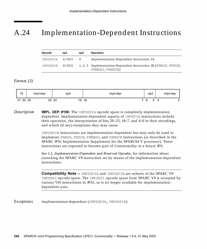
Implementation-Dependent Instructions
A.24 Implementation-Dependent Instructions
Format (3)
Description IMPL. DEP. #106: The IMPDEP2A opcode space is completely implementation dependent. Implementation-dependent aspects of IMDEP2A instructions include their operation, the interpretation of bits 29–25, 18–7, and 4–0 in their encodings, and which (if any) exceptions they may cause.
IMPDEP2B instructions are implementation dependent but may only be used to implement FMADD, FMSUB, FNMADD, and FNMSUB instructions (as described in the SPARC JPS1 Implementation Supplement for the SPARC64 V processor). These instructions are expected to become part of Commonality in a future JPS.
See I.2, Implementation-Dependent and Reserved Opcodes, for information about extending the SPARC V9 instruction set by means of the implementation-dependent instructions.
Compatibility Note – IMPDEP2A and IMPDEP2B are subsets of the SPARC V9 IMPDEP2 opcode space. The IMPDEP1 opcode space from SPARC V9 is occupied by various VIS instructions in JPS1, so is no longer available for implementation-dependent uses.
Exceptions implementation-dependent (IMPDEP2A, IMPDEP2B)
Opcode op3 op2 Operation
IMPDEP2A 11 0111 0 Implementation-Dependent Instruction 2A
IMPDEP2B 11 0111 1, 2, 3 Implementation-Dependent Instruction 2B (FMADD, FMSUB, FNMADD, FNMSUB)
10 op3 impl-depimpl-dep
31 1824 02530 29 19
impl-dep
7 6 5 4
op2
240 SPARC® Joint Programming Specification (JPS1): Commonality • Release 1.0.4, 31 May 2002
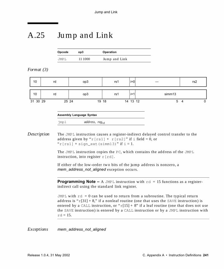
Jump and Link
A.25 Jump and Link
Format (3)
Description The JMPL instruction causes a register-indirect delayed control transfer to the address given by “r[rs1] + r[rs2]” if i field = 0, or “r[rs1] + sign_ext(simm13)” if i = 1.
The JMPL instruction copies the PC, which contains the address of the JMPL instruction, into register r[rd].
If either of the low-order two bits of the jump address is nonzero, a mem_address_not_aligned exception occurs.
Programming Note – A JMPL instruction with rd = 15 functions as a register-indirect call using the standard link register.
JMPL with rd = 0 can be used to return from a subroutine. The typical return address is “r[31] + 8,” if a nonleaf routine (one that uses the SAVE instruction) is entered by a CALL instruction, or “r[15] + 8” if a leaf routine (one that does not use the SAVE instruction) is entered by a CALL instruction or by a JMPL instruction with rd = 15.
Exceptions mem_address_not_aligned
Opcode op3 Operation
JMPL 11 1000 Jump and Link
Assembly Language Syntax
jmpl address, regrd
31 24 02530 29 19 18
rd10 op3
14 13 12 5 4
rs1 rs2i=0
rd10 op3 rs1 simm13i=1
—
Release 1.0.4, 31 May 2002 C. Appendix A • Instruction Definitions 241
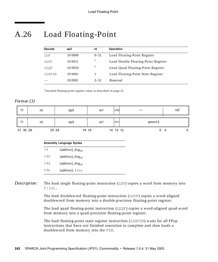
Load Floating-Point
A.26 Load Floating-Point
† Encoded floating-point register value, as described on page 52.
Format (3)
Description: The load single floating-point instruction (LDF) copies a word from memory into f[rd].
The load doubleword floating-point instruction (LDDF) copies a word-aligned doubleword from memory into a double-precision floating-point register.
The load quad floating-point instruction (LDQF) copies a word-aligned quad-word from memory into a quad-precision floating-point register.
The load floating-point state register instruction (LDXFSR) waits for all FPop instructions that have not finished execution to complete and then loads a doubleword from memory into the FSR.
Opcode op3 rd Operation
LDF 10 0000 0–31 Load Floating-Point Register
LDDF 10 0011 † Load Double Floating-Point Register
LDQF 10 0010 † Load Quad Floating-Point Register
LDXFSR 10 0001 1 Load Floating-Point State Register
— 10 0001 2–31 Reserved
Assembly Language Syntax
ld [address], fregrd
ldd [address], fregrd
ldq [address], fregrd
ldx [address], %fsr
31 24 02530 29 19 18 14 13 12 5 4
rd11 op3 rs1 simm13i=1
rd11 op3 rs1 i=0 — rs2
242 SPARC® Joint Programming Specification (JPS1): Commonality • Release 1.0.4, 31 May 2002
Load Floating-Point
Load floating-point instructions access the primary address space (ASI = 8016). The effective address for these instructions is “r[rs1] + r[rs2]” if i = 0, or “r[rs1] + sign_ext(simm13)” if i = 1.
LDF causes a mem_address_not_aligned exception if the effective memory address is not word aligned. LDXFSR causes a mem_address_not_aligned exception if the address is not doubleword aligned. If the floating-point unit is not enabled (per FPRS.FEF and PSTATE.PEF) or if no FPU is present, then a load floating-point instruction causes an fp_disabled exception.
IMPL. DEP. #109(1): LDDF requires only word alignment. However, if the effective address is word aligned but not doubleword aligned, LDDF may cause an LDDF_mem_address_not_aligned exception. In this case, the trap handler software shall emulate the LDDF instruction and return.
IMPL. DEP. #111(1): LDQF requires only word alignment. However, if the effective address is word aligned but not quadword aligned, LDQF may cause an LDQF_mem_address_not_aligned exception. In this case, the trap handler software shall emulate the LDQF instruction and return.
Programming Note – In SPARC V8, some compilers issued sequences of single-precision loads when they could not determine that doubleword or quadword operands were properly aligned. For SPARC V9, since emulation of misaligned loads is expected to be fast, we recommend that compilers issue sets of single-precision loads only when they can determine that doubleword or quadword operands are not properly aligned.
IMPL. DEP. #44 (1): If a load floating-point instruction traps with any type of access error, the contents of the destination floating-point register(s) remain unchanged or are undefined.
Exceptions illegal_instruction (op3=2116 and rd = 2–31)fp_disabled LDDF_mem_address_not_aligned (LDDF only)LDQF_mem_address_not_aligned (LDQF only) (not used in JPS1)mem_address_not_aligned data_access_exceptionPA_watchpointVA_watchpointdata_access_errorfast_data_access_MMU_missfast_data_access_protection
Release 1.0.4, 31 May 2002 C. Appendix A • Instruction Definitions 243
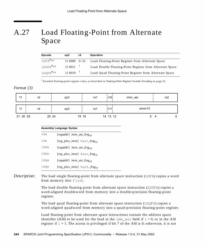
Load Floating-Point from Alternate Space
A.27 Load Floating-Point from Alternate Space
† Encoded floating-point register value, as described in Floating-Point Register Number Encoding on page 52.
Format (3)
Description: The load single floating-point from alternate space instruction (LDFA) copies a word from memory into f[rd].
The load double floating-point from alternate space instruction (LDDFA) copies a word-aligned doubleword from memory into a double-precision floating-point register.
The load quad floating-point from alternate space instruction (LDQFA) copies a word-aligned quadword from memory into a quad-precision floating-point register.
Load floating-point from alternate space instructions contain the address space identifier (ASI) to be used for the load in the imm_asi field if i = 0, or in the ASI register if i = 1. The access is privileged if bit 7 of the ASI is 0; otherwise, it is not
Opcode op3 rd Operation
LDFAPASI 11 0000 0–31 Load Floating-Point Register from Alternate Space
LDDFAPASI 11 0011 † Load Double Floating-Point Register from Alternate Space
LDQFAPASI 11 0010 † Load Quad Floating-Point Register from Alternate Space
Assembly Language Syntax
lda [regaddr] imm_asi, fregrd
lda [reg_plus_imm] %asi, fregrd
ldda [regaddr] imm_asi, fregrd
ldda [reg_plus_imm] %asi, fregrd
ldqa [regaddr] imm_asi, fregrd
ldqa [reg_plus_imm] %asi, fregrd
31 24 02530 29 19 18
rd11 op3 imm_asi
14 13 12 5 4
rs1 rs2i=0
rd11 op3 rs1 i=1 simm13
244 SPARC® Joint Programming Specification (JPS1): Commonality • Release 1.0.4, 31 May 2002
Load Floating-Point from Alternate Space
privileged. The effective address for these instructions is “r[rs1] + r[rs2]” if i = 0, or “r[rs1] + sign_ext(simm13)” if i = 1.
LDFA causes a mem_address_not_aligned exception if the effective memory address is not word aligned. If the floating-point unit is not enabled (per FPRS.FEF and PSTATE.PEF) or if no FPU is present, then load floating-point from alternate space instructions cause an fp_disabled exception.
LDDFA with certain target ASIs is defined to be a 64-byte block-load instruction. See Block Load and Store (VIS I) on page 199 for details.
LDDFA with certain target ASIs is defined to be a Short Floating-point Load instruction. See Short Floating-Point Load and Store (VIS I) on page 326 for details.
Implementation Note – LDFA, LDDFA, and LDQFA cause a privileged_action exception if PSTATE.PRIV = 0 and bit 7 of the ASI is 0.
IMPL. DEP. #109(2): LDDFA requires only word alignment. However, if the effective address is word aligned but not doubleword aligned, LDDFA may cause an LDDF_mem_address_not_aligned exception. In this case, the trap handler software shall emulate the LDDF instruction and return.
IMPL. DEP. #111(2): LDQFA requires only word alignment. However, if the effective address is word aligned but not quadword aligned, LDQFA may cause an LDQF_mem_address_not_aligned exception. In this case, the trap handler software shall emulate the LDQF instruction and return.
Programming Note – In SPARC V8, some compilers issued sequences of single-precision loads when they could not determine that doubleword or quadword operands were properly aligned. For SPARC V9, since emulation of misaligned loads is expected to be fast, compilers should issue sets of single-precision loads only when they can determine that doubleword or quadword operands are not properly aligned.
IMPL. DEP. #44 (2): If a load floating-point instruction traps with any type of access error, the destination floating-point register(s) remain unchanged or are undefined.
Exceptions illegal_instruction (LDQFA only)fp_disabled LDDF_mem_address_not_aligned (LDDFA only)LDQF_mem_address_not_aligned (LDQFA only) (not used in JPS1)mem_address_not_aligned privileged_action data_access_exceptiondata_access_errorfast_data_access_MMU_miss
Release 1.0.4, 31 May 2002 C. Appendix A • Instruction Definitions 245
Load Floating-Point from Alternate Space
fast_data_access_protectionVA_watchpointPA_watchpoint
246 SPARC® Joint Programming Specification (JPS1): Commonality • Release 1.0.4, 31 May 2002
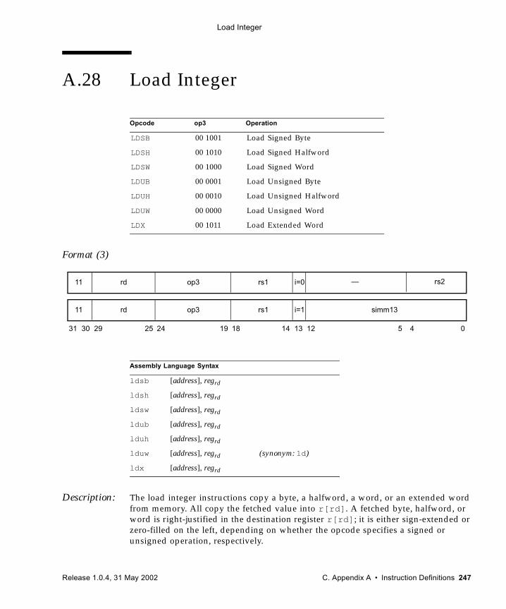
Load Integer
A.28 Load Integer
Format (3)
Description: The load integer instructions copy a byte, a halfword, a word, or an extended word from memory. All copy the fetched value into r[rd]. A fetched byte, halfword, or word is right-justified in the destination register r[rd]; it is either sign-extended or zero-filled on the left, depending on whether the opcode specifies a signed or unsigned operation, respectively.
Opcode op3 Operation
LDSB 00 1001 Load Signed Byte
LDSH 00 1010 Load Signed Halfword
LDSW 00 1000 Load Signed Word
LDUB 00 0001 Load Unsigned Byte
LDUH 00 0010 Load Unsigned Halfword
LDUW 00 0000 Load Unsigned Word
LDX 00 1011 Load Extended Word
Assembly Language Syntax
ldsb [address], regrd
ldsh [address], regrd
ldsw [address], regrd
ldub [address], regrd
lduh [address], regrd
lduw [address], regrd (synonym: ld)
ldx [address], regrd
31 24 02530 29 19 18 14 13 12 5 4
rd11 op3 rs1 simm13i=1
rd11 op3 rs1 i=0 — rs2
Release 1.0.4, 31 May 2002 C. Appendix A • Instruction Definitions 247
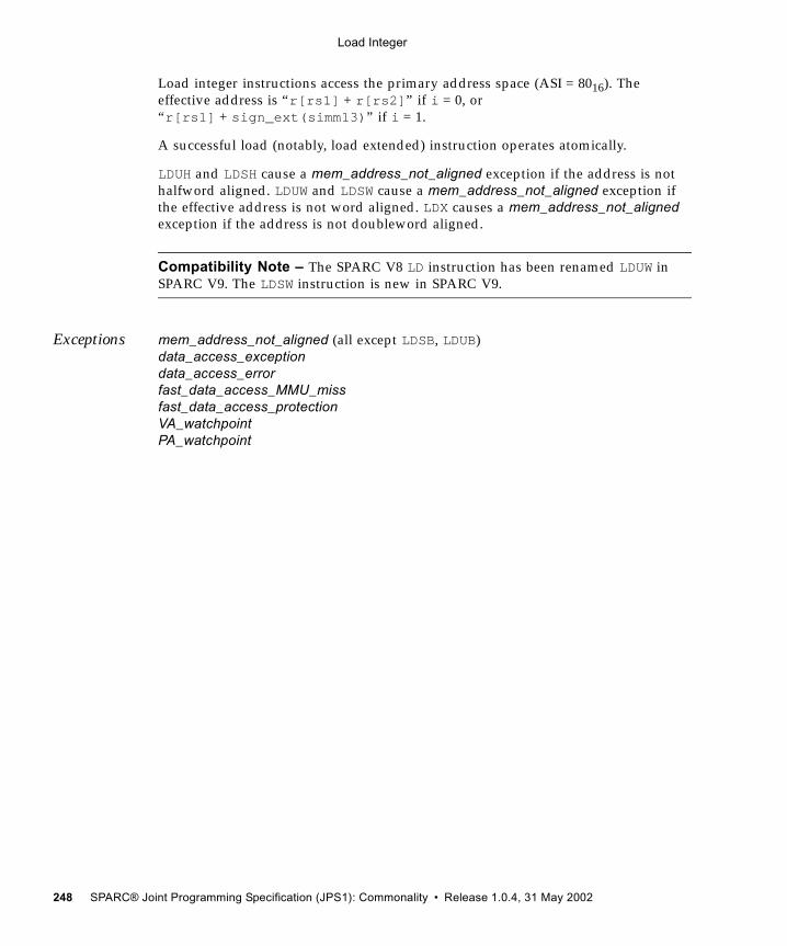
Load Integer
Load integer instructions access the primary address space (ASI = 8016). The effective address is “r[rs1] + r[rs2]” if i = 0, or “r[rs1] + sign_ext(simm13)” if i = 1.
A successful load (notably, load extended) instruction operates atomically.
LDUH and LDSH cause a mem_address_not_aligned exception if the address is not halfword aligned. LDUW and LDSW cause a mem_address_not_aligned exception if the effective address is not word aligned. LDX causes a mem_address_not_aligned exception if the address is not doubleword aligned.
Compatibility Note – The SPARC V8 LD instruction has been renamed LDUW in SPARC V9. The LDSW instruction is new in SPARC V9.
Exceptions mem_address_not_aligned (all except LDSB, LDUB)data_access_exceptiondata_access_errorfast_data_access_MMU_missfast_data_access_protectionVA_watchpointPA_watchpoint
248 SPARC® Joint Programming Specification (JPS1): Commonality • Release 1.0.4, 31 May 2002
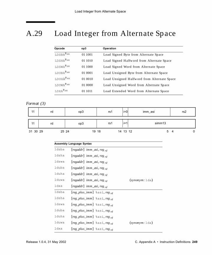
Load Integer from Alternate Space
A.29 Load Integer from Alternate Space
Format (3)
Opcode op3 Operation
LDSBAPASI 01 1001 Load Signed Byte from Alternate Space
LDSHAPASI 01 1010 Load Signed Halfword from Alternate Space
LDSWAPASI 01 1000 Load Signed Word from Alternate Space
LDUBAPASI 01 0001 Load Unsigned Byte from Alternate Space
LDUHAPASI 01 0010 Load Unsigned Halfword from Alternate Space
LDUWAPASI 01 0000 Load Unsigned Word from Alternate Space
LDXAPASI 01 1011 Load Extended Word from Alternate Space
Assembly Language Syntax
ldsba [regaddr] imm_asi, reg rd
ldsha [regaddr] imm_asi, reg rd
ldswa [regaddr] imm_asi, reg rd
lduba [regaddr] imm_asi, reg rd
lduha [regaddr] imm_asi, reg rd
lduwa [regaddr] imm_asi, reg rd (synonym: lda)
ldxa [regaddr] imm_asi, reg rd
ldsba [reg_plus_imm] %asi, reg rd
ldsha [reg_plus_imm] %asi, reg rd
ldswa [reg_plus_imm] %asi, reg rd
lduba [reg_plus_imm] %asi, reg rd
lduha [reg_plus_imm] %asi, reg rd
lduwa [reg_plus_imm] %asi, reg rd (synonym: lda)
ldxa [reg_plus_imm] %asi, reg rd
31 24 02530 29 19 18
rd11 op3 imm_asi
14 13 12 5 4
rs1 rs2i=0
rd11 op3 rs1 i=1 simm13
Release 1.0.4, 31 May 2002 C. Appendix A • Instruction Definitions 249
Load Integer from Alternate Space
Description The load integer from alternate space instructions copy a byte, a halfword, a word, or an extended word from memory. All copy the fetched value into r[rd]. A fetched byte, halfword, or word is right-justified in the destination register r[rd]; it is either sign-extended or zero-filled on the left, depending on whether the opcode specifies a signed or unsigned operation, respectively.
The load integer from alternate space instructions contain the address space identifier (ASI) to be used for the load in the imm_asi field if i = 0, or in the ASI register if i = 1. The access is privileged if bit 7 of the ASI is 0; otherwise, it is not privileged. The effective address for these instructions is “r[rs1] + r[rs2]” if i = 0, or “r[rs1] + sign_ext(simm13)” if i = 1.
A successful load (notably, load extended) instruction operates atomically.
LDUHA and LDSHA cause a mem_address_not_aligned exception if the address is not halfword aligned. LDUWA and LDSWA cause a mem_address_not_aligned exception if the effective address is not word aligned; LDXA causes a mem_address_not_aligned exception if the address is not doubleword aligned.
These instructions cause a privileged_action exception if PSTATE.PRIV = 0 and bit 7 of the ASI is 0.
Exceptions privileged_actionmem_address_not_aligned (all except LDSBA and LDUBA)data_access_exceptionPA_watchpointVA_watchpointfast_data_access_MMU_missfast_data_access_protectiondata_access_error
250 SPARC® Joint Programming Specification (JPS1): Commonality • Release 1.0.4, 31 May 2002
Load Quadword, Atomic (VIS I)
A.30 Load Quadword, Atomic (VIS I)
Format (3) LDDA
Description ASIs 2416 and 2C16 are used with the LDDA instruction to atomically read a 128-bit, virtually addressed data item. They are intended to be used by a TLB miss handler to access TSB entries without requiring locks. The data are placed in an even/odd pair of 64-bit registers. The lowest-address 64 bits are placed in the even register; the highest-address 64 bits are placed in the odd-numbered register. The reference is made from the nucleus context.
In addition to the usual traps for LDDA using a privileged ASI, a data_access_exception trap occurs for a noncacheable access or if a quadword-load ASI is used with any instruction other than LDDA. A mem_address_not_aligned trap is taken if the access is not aligned on a 16-byte boundary.
With respect to little endian memory, a Load Quadword Atomic instruction behaves as if it comprises two 64-bit loads, each of which is byte-swapped independently before being written into its respective destination register.
Exceptions: privileged_actionPA_watchpoint (recognized on only the first 8 bytes of an access)VA_watchpoint (recognized on only the first 8 bytes of an access)illegal_instruction (misaligned rd)mem_address_not_aligned
Opcode imm_asi ASI Value Operation
LDDA ASI_NUCLEUS_QUAD_LDD 2416 128-bit atomic load
LDDA ASI_NUCLEUS_QUAD_LDD_L 2C16 128-bit atomic load, little-endian
Assembly Language Syntax
ldda [reg_addr] imm_asi, regrd
ldda [reg_plus_imm] %asi, regrd
31 24 02530 29 19 18 14 13 5 4
rd11 010011 simm_13rs1 i=1
rd11 010011 imm_asirs1 rs2i=0
Release 1.0.4, 31 May 2002 C. Appendix A • Instruction Definitions 251
Load Quadword, Atomic (VIS I)
data_access_exception (an attempt to access a page marked as noncacheable)data_access_errorfast_data_access_MMU_missfast_data_access_protection
252 SPARC® Joint Programming Specification (JPS1): Commonality • Release 1.0.4, 31 May 2002
Load-Store Unsigned Byte
A.31 Load-Store Unsigned Byte
Format (3)
Description The load-store unsigned byte instruction copies a byte from memory into r[rd], then rewrites the addressed byte in memory to all 1’s. The fetched byte is right-justified in the destination register r[rd] and zero-filled on the left.
The operation is performed atomically, that is, without allowing intervening interrupts or deferred traps. In a multiprocessor system, two or more processors executing LDSTUB, LDSTUBA, CASA, CASXA, SWAP, or SWAPA instructions addressing all or parts of the same doubleword simultaneously are guaranteed to execute them in an undefined, but serial, order.
The effective address for these instructions is “r[rs1] + r[rs2]” if i = 0, or “r[rs1] + sign_ext(simm13)” if i = 1.
The coherence and atomicity of memory operations between processors and I/O DMA memory accesses are implementation dependent (impl. dep. #120).
Exceptions data_access_exceptiondata_access_errorfast_data_access_MMU_missfast_data_access_protectionVA_watchpointPA_watchpoint
Opcode op3 Operation
LDSTUB 00 1101 Load-Store Unsigned Byte
Assembly Language Syntax
ldstub [address], regrd
31 24 02530 29 19 18 14 13 12 5 4
rd11 op3 rs1 simm13i=1
rd11 op3 rs1 i=0 — rs2
Release 1.0.4, 31 May 2002 C. Appendix A • Instruction Definitions 253
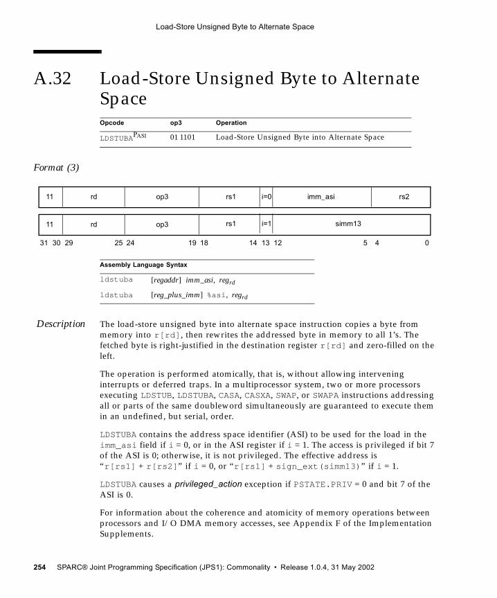
Load-Store Unsigned Byte to Alternate Space
A.32 Load-Store Unsigned Byte to Alternate Space
Format (3)
Description The load-store unsigned byte into alternate space instruction copies a byte from memory into r[rd], then rewrites the addressed byte in memory to all 1’s. The fetched byte is right-justified in the destination register r[rd] and zero-filled on the left.
The operation is performed atomically, that is, without allowing intervening interrupts or deferred traps. In a multiprocessor system, two or more processors executing LDSTUB, LDSTUBA, CASA, CASXA, SWAP, or SWAPA instructions addressing all or parts of the same doubleword simultaneously are guaranteed to execute them in an undefined, but serial, order.
LDSTUBA contains the address space identifier (ASI) to be used for the load in the imm_asi field if i = 0, or in the ASI register if i = 1. The access is privileged if bit 7 of the ASI is 0; otherwise, it is not privileged. The effective address is “r[rs1] + r[rs2]” if i = 0, or “r[rs1] + sign_ext(simm13)” if i = 1.
LDSTUBA causes a privileged_action exception if PSTATE.PRIV = 0 and bit 7 of the ASI is 0.
For information about the coherence and atomicity of memory operations between processors and I/O DMA memory accesses, see Appendix F of the Implementation Supplements.
Opcode op3 Operation
LDSTUBAPASI 01 1101 Load-Store Unsigned Byte into Alternate Space
Assembly Language Syntax
ldstuba [regaddr] imm_asi, regrd
ldstuba [reg_plus_imm] %asi, regrd
31 24 02530 29 19 18
rd11 op3 imm_asi
14 13 12 5 4
rs1 rs2i=0
rd11 op3 rs1 i=1 simm13
254 SPARC® Joint Programming Specification (JPS1): Commonality • Release 1.0.4, 31 May 2002
Load-Store Unsigned Byte to Alternate Space
Exceptions privileged_action data_access_exceptiondata_access_errorfast_data_access_MMU_missfast_data_access_protectionVA_watchpointPA_watchpoint
Release 1.0.4, 31 May 2002 C. Appendix A • Instruction Definitions 255
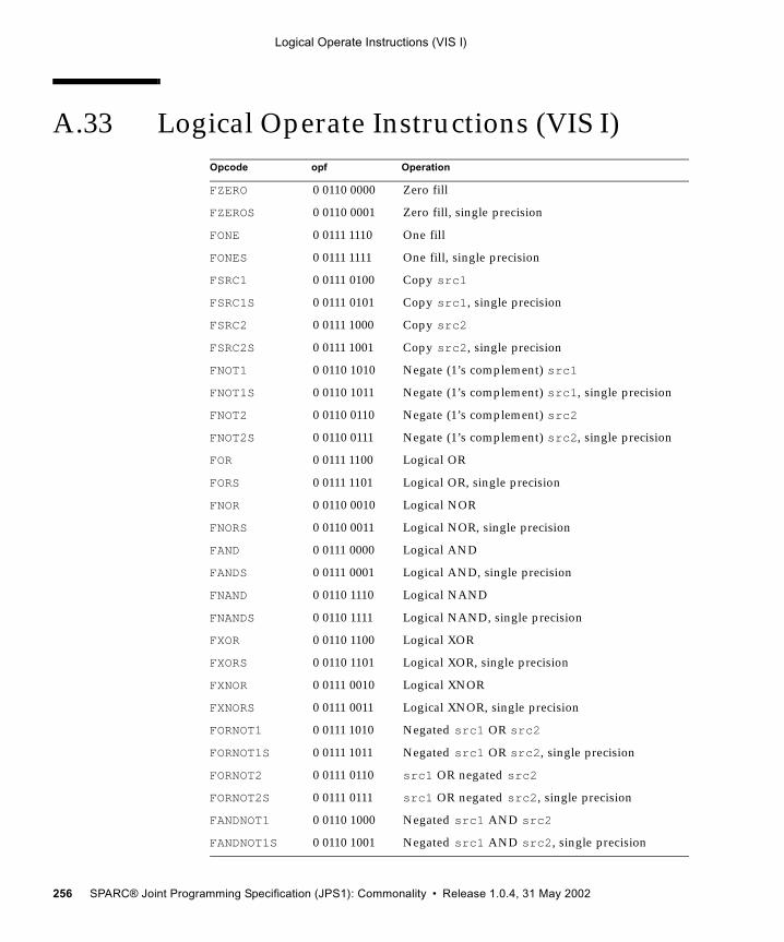
Logical Operate Instructions (VIS I)
A.33 Logical Operate Instructions (VIS I) Opcode opf Operation
FZERO 0 0110 0000 Zero fill
FZEROS 0 0110 0001 Zero fill, single precision
FONE 0 0111 1110 One fill
FONES 0 0111 1111 One fill, single precision
FSRC1 0 0111 0100 Copy src1
FSRC1S 0 0111 0101 Copy src1, single precision
FSRC2 0 0111 1000 Copy src2
FSRC2S 0 0111 1001 Copy src2, single precision
FNOT1 0 0110 1010 Negate (1’s complement) src1
FNOT1S 0 0110 1011 Negate (1’s complement) src1, single precision
FNOT2 0 0110 0110 Negate (1’s complement) src2
FNOT2S 0 0110 0111 Negate (1’s complement) src2, single precision
FOR 0 0111 1100 Logical OR
FORS 0 0111 1101 Logical OR, single precision
FNOR 0 0110 0010 Logical NOR
FNORS 0 0110 0011 Logical NOR, single precision
FAND 0 0111 0000 Logical AND
FANDS 0 0111 0001 Logical AND, single precision
FNAND 0 0110 1110 Logical NAND
FNANDS 0 0110 1111 Logical NAND, single precision
FXOR 0 0110 1100 Logical XOR
FXORS 0 0110 1101 Logical XOR, single precision
FXNOR 0 0111 0010 Logical XNOR
FXNORS 0 0111 0011 Logical XNOR, single precision
FORNOT1 0 0111 1010 Negated src1 OR src2
FORNOT1S 0 0111 1011 Negated src1 OR src2, single precision
FORNOT2 0 0111 0110 src1 OR negated src2
FORNOT2S 0 0111 0111 src1 OR negated src2, single precision
FANDNOT1 0 0110 1000 Negated src1 AND src2
FANDNOT1S 0 0110 1001 Negated src1 AND src2, single precision
256 SPARC® Joint Programming Specification (JPS1): Commonality • Release 1.0.4, 31 May 2002
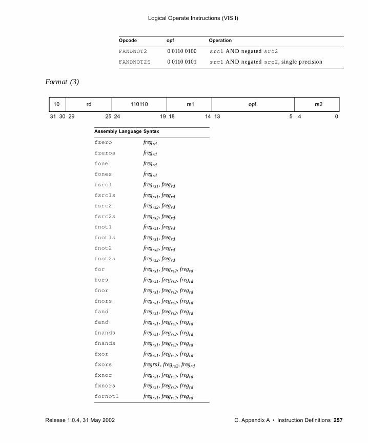
Logical Operate Instructions (VIS I)
Format (3)
FANDNOT2 0 0110 0100 src1 AND negated src2
FANDNOT2S 0 0110 0101 src1 AND negated src2, single precision
Assembly Language Syntax
fzero fregrd
fzeros fregrd
fone fregrd
fones fregrd
fsrc1 fregrs1, fregrd
fsrc1s fregrs1, fregrd
fsrc2 fregrs2, fregrd
fsrc2s fregrs2, fregrd
fnot1 fregrs1, fregrd
fnot1s fregrs1, fregrd
fnot2 fregrs2, fregrd
fnot2s fregrs2, fregrd
for fregrs1, fregrs2, fregrd
fors fregrs1, fregrs2, fregrd
fnor fregrs1, fregrs2, fregrd
fnors fregrs1, fregrs2, fregrd
fand fregrs1, fregrs2, fregrd
fand fregrs1, fregrs2, fregrd
fnands fregrs1, fregrs2, fregrd
fnands fregrs1, fregrs2, fregrd
fxor fregrs1, fregrs2, fregrd
fxors fregrs1, fregrs2, fregrd
fxnor fregrs1, fregrs2, fregrd
fxnors fregrs1, fregrs2, fregrd
fornot1 fregrs1, fregrs2, fregrd
Opcode opf Operation
31 24 02530 29 19 18 14 13 5 4
rd10 110110 opfrs1 rs2
Release 1.0.4, 31 May 2002 C. Appendix A • Instruction Definitions 257
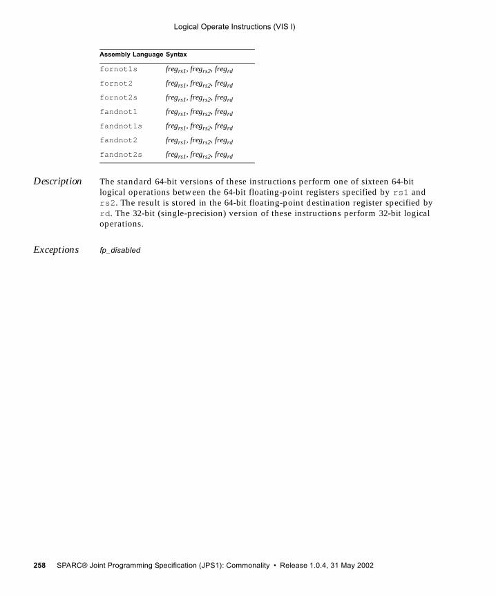
Logical Operate Instructions (VIS I)
Description The standard 64-bit versions of these instructions perform one of sixteen 64-bit logical operations between the 64-bit floating-point registers specified by rs1 and rs2. The result is stored in the 64-bit floating-point destination register specified by rd. The 32-bit (single-precision) version of these instructions perform 32-bit logical operations.
Exceptions fp_disabled
fornot1s fregrs1, fregrs2, fregrd
fornot2 fregrs1, fregrs2, fregrd
fornot2s fregrs1, fregrs2, fregrd
fandnot1 fregrs1, fregrs2, fregrd
fandnot1s fregrs1, fregrs2, fregrd
fandnot2 fregrs1, fregrs2, fregrd
fandnot2s fregrs1, fregrs2, fregrd
Assembly Language Syntax
258 SPARC® Joint Programming Specification (JPS1): Commonality • Release 1.0.4, 31 May 2002
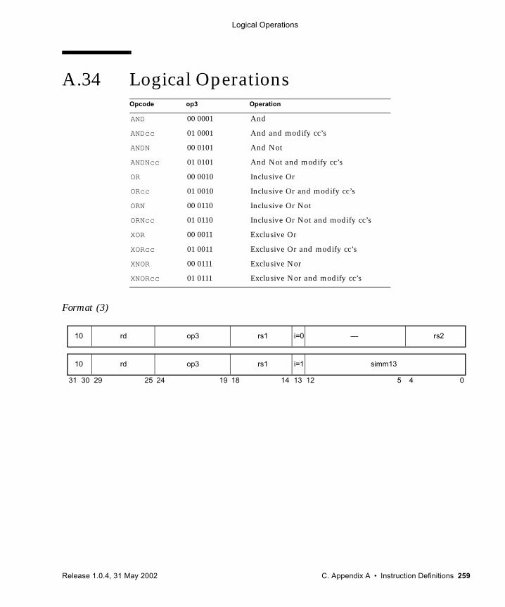
Logical Operations
A.34 Logical Operations
Format (3)
Opcode op3 Operation
AND 00 0001 And
ANDcc 01 0001 And and modify cc’s
ANDN 00 0101 And Not
ANDNcc 01 0101 And Not and modify cc’s
OR 00 0010 Inclusive Or
ORcc 01 0010 Inclusive Or and modify cc’s
ORN 00 0110 Inclusive Or Not
ORNcc 01 0110 Inclusive Or Not and modify cc’s
XOR 00 0011 Exclusive Or
XORcc 01 0011 Exclusive Or and modify cc’s
XNOR 00 0111 Exclusive Nor
XNORcc 01 0111 Exclusive Nor and modify cc’s
31 24 02530 29 19 18
rd10 op3 —
14 13 12 5 4
rs1 rs2i=0
rd10 op3 rs1 simm13i=1
Release 1.0.4, 31 May 2002 C. Appendix A • Instruction Definitions 259
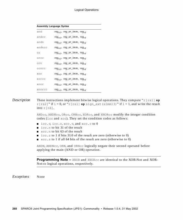
Logical Operations
Description These instructions implement bitwise logical operations. They compute “r[rs1] op r[rs2]” if i = 0, or “r[rs1] op sign_ext(simm13)” if i = 1, and write the result into r[rd].
ANDcc, ANDNcc, ORcc, ORNcc, XORcc, and XNORcc modify the integer condition codes (icc and xcc). They set the condition codes as follows:
■ icc.v, icc.c, xcc.v, and xcc.c to 0■ icc.n to bit 31 of the result■ xcc.n to bit 63 of the result■ icc.z to 1 if bits 31:0 of the result are zero (otherwise to 0)■ xcc.z to 1 if all 64 bits of the result are zero (otherwise to 0)
ANDN, ANDNcc, ORN, and ORNcc logically negate their second operand before applying the main (AND or OR) operation.
Programming Note – XNOR and XNORcc are identical to the XOR-Not and XOR-Not-cc logical operations, respectively.
Exceptions None
Assembly Language Syntax
and regrs1, reg_or_imm, regrd
andcc regrs1, reg_or_imm, regrd
andn regrs1, reg_or_imm, regrd
andncc regrs1, reg_or_imm, regrd
or regrs1, reg_or_imm, regrd
orcc regrs1, reg_or_imm, regrd
orn regrs1, reg_or_imm, regrd
orncc regrs1, reg_or_imm, regrd
xor regrs1, reg_or_imm, regrd
xorcc regrs1, reg_or_imm, regrd
xnor regrs1, reg_or_imm, regrd
xnorcc regrs1, reg_or_imm, regrd
260 SPARC® Joint Programming Specification (JPS1): Commonality • Release 1.0.4, 31 May 2002
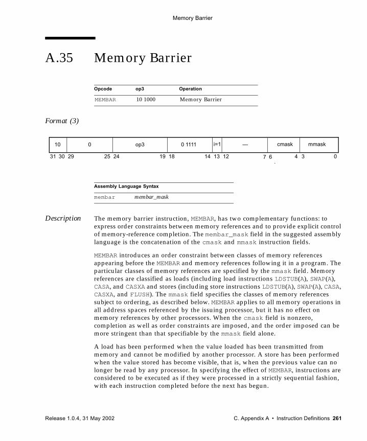
Memory Barrier
A.35 Memory Barrier
Format (3)
Description The memory barrier instruction, MEMBAR, has two complementary functions: to express order constraints between memory references and to provide explicit control of memory-reference completion. The membar_mask field in the suggested assembly language is the concatenation of the cmask and mmask instruction fields.
MEMBAR introduces an order constraint between classes of memory references appearing before the MEMBAR and memory references following it in a program. The particular classes of memory references are specified by the mmask field. Memory references are classified as loads (including load instructions LDSTUB(A), SWAP(A), CASA, and CASXA and stores (including store instructions LDSTUB(A), SWAP(A), CASA, CASXA, and FLUSH). The mmask field specifies the classes of memory references subject to ordering, as described below. MEMBAR applies to all memory operations in all address spaces referenced by the issuing processor, but it has no effect on memory references by other processors. When the cmask field is nonzero, completion as well as order constraints are imposed, and the order imposed can be more stringent than that specifiable by the mmask field alone.
A load has been performed when the value loaded has been transmitted from memory and cannot be modified by another processor. A store has been performed when the value stored has become visible, that is, when the previous value can no longer be read by any processor. In specifying the effect of MEMBAR, instructions are considered to be executed as if they were processed in a strictly sequential fashion, with each instruction completed before the next has begun.
Opcode op3 Operation
MEMBAR 10 1000 Memory Barrier
Assembly Language Syntax
membar membar_mask
31 141924 18 13 12 02530 29
10 0 op3 0 1111 i=1 —
4 3
mmask
6
4
7
cmask
Release 1.0.4, 31 May 2002 C. Appendix A • Instruction Definitions 261
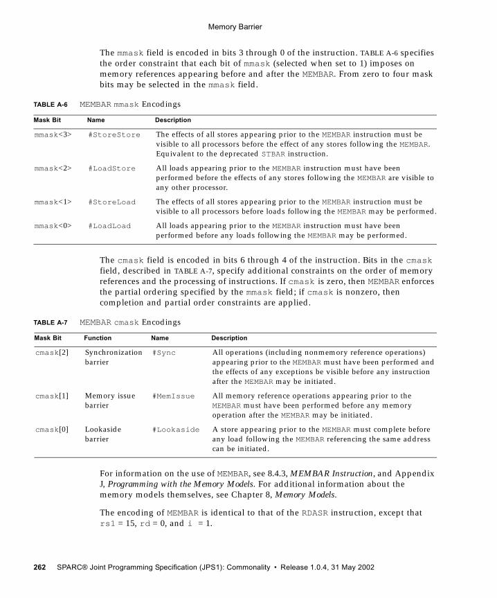
Memory Barrier
The mmask field is encoded in bits 3 through 0 of the instruction. TABLE A-6 specifies the order constraint that each bit of mmask (selected when set to 1) imposes on memory references appearing before and after the MEMBAR. From zero to four mask bits may be selected in the mmask field.
The cmask field is encoded in bits 6 through 4 of the instruction. Bits in the cmask field, described in TABLE A-7, specify additional constraints on the order of memory references and the processing of instructions. If cmask is zero, then MEMBAR enforces the partial ordering specified by the mmask field; if cmask is nonzero, then completion and partial order constraints are applied.
For information on the use of MEMBAR, see 8.4.3, MEMBAR Instruction, and Appendix J, Programming with the Memory Models. For additional information about the memory models themselves, see Chapter 8, Memory Models.
The encoding of MEMBAR is identical to that of the RDASR instruction, except that rs1 = 15, rd = 0, and i = 1.
TABLE A-6 MEMBAR mmask Encodings
Mask Bit Name Description
mmask<3> #StoreStore The effects of all stores appearing prior to the MEMBAR instruction must be visible to all processors before the effect of any stores following the MEMBAR. Equivalent to the deprecated STBAR instruction.
mmask<2> #LoadStore All loads appearing prior to the MEMBAR instruction must have been performed before the effects of any stores following the MEMBAR are visible to any other processor.
mmask<1> #StoreLoad The effects of all stores appearing prior to the MEMBAR instruction must be visible to all processors before loads following the MEMBAR may be performed.
mmask<0> #LoadLoad All loads appearing prior to the MEMBAR instruction must have been performed before any loads following the MEMBAR may be performed.
TABLE A-7 MEMBAR cmask Encodings
Mask Bit Function Name Description
cmask[2] Synchronizationbarrier
#Sync All operations (including nonmemory reference operations) appearing prior to the MEMBAR must have been performed and the effects of any exceptions be visible before any instruction after the MEMBAR may be initiated.
cmask[1] Memory issuebarrier
#MemIssue All memory reference operations appearing prior to the MEMBAR must have been performed before any memory operation after the MEMBAR may be initiated.
cmask[0] Lookasidebarrier
#Lookaside A store appearing prior to the MEMBAR must complete before any load following the MEMBAR referencing the same address can be initiated.
262 SPARC® Joint Programming Specification (JPS1): Commonality • Release 1.0.4, 31 May 2002
Memory Barrier
The coherence and atomicity of memory operations between processors and I/O DMA memory accesses are implementation dependent (impl. dep. #120).
Compatibility Note – MEMBAR with mmask = 816 and cmask = 016 (“membar #StoreStore”) is identical in function to the SPARC V8 STBAR instruction, which is deprecated.
Exceptions None
Release 1.0.4, 31 May 2002 C. Appendix A • Instruction Definitions 263
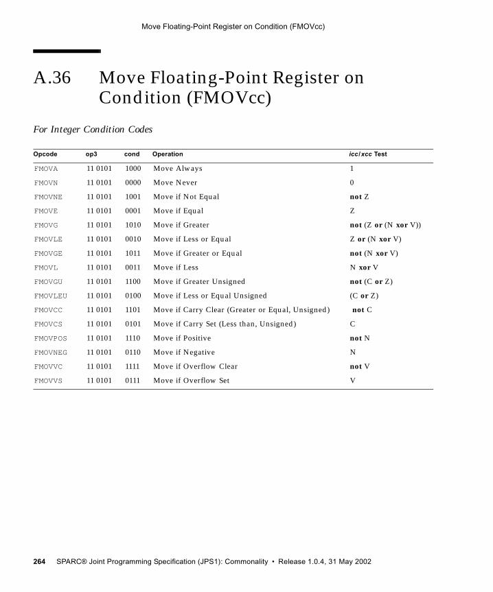
Move Floating-Point Register on Condition (FMOVcc)
A.36 Move Floating-Point Register on Condition (FMOVcc)
For Integer Condition Codes
Opcode op3 cond Operation icc /xcc Test
FMOVA 11 0101 1000 Move Always 1
FMOVN 11 0101 0000 Move Never 0
FMOVNE 11 0101 1001 Move if Not Equal not Z
FMOVE 11 0101 0001 Move if Equal Z
FMOVG 11 0101 1010 Move if Greater not (Z or (N xor V))
FMOVLE 11 0101 0010 Move if Less or Equal Z or (N xor V)
FMOVGE 11 0101 1011 Move if Greater or Equal not (N xor V)
FMOVL 11 0101 0011 Move if Less N xor V
FMOVGU 11 0101 1100 Move if Greater Unsigned not (C or Z)
FMOVLEU 11 0101 0100 Move if Less or Equal Unsigned (C or Z)
FMOVCC 11 0101 1101 Move if Carry Clear (Greater or Equal, Unsigned) not C
FMOVCS 11 0101 0101 Move if Carry Set (Less than, Unsigned) C
FMOVPOS 11 0101 1110 Move if Positive not N
FMOVNEG 11 0101 0110 Move if Negative N
FMOVVC 11 0101 1111 Move if Overflow Clear not V
FMOVVS 11 0101 0111 Move if Overflow Set V
264 SPARC® Joint Programming Specification (JPS1): Commonality • Release 1.0.4, 31 May 2002
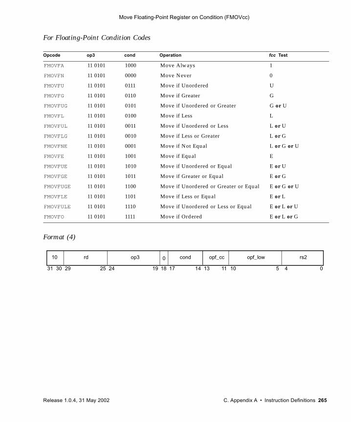
Move Floating-Point Register on Condition (FMOVcc)
For Floating-Point Condition Codes
Format (4)
Opcode op3 cond Operation fcc Test
FMOVFA 11 0101 1000 Move Always 1
FMOVFN 11 0101 0000 Move Never 0
FMOVFU 11 0101 0111 Move if Unordered U
FMOVFG 11 0101 0110 Move if Greater G
FMOVFUG 11 0101 0101 Move if Unordered or Greater G or U
FMOVFL 11 0101 0100 Move if Less L
FMOVFUL 11 0101 0011 Move if Unordered or Less L or U
FMOVFLG 11 0101 0010 Move if Less or Greater L or G
FMOVFNE 11 0101 0001 Move if Not Equal L or G or U
FMOVFE 11 0101 1001 Move if Equal E
FMOVFUE 11 0101 1010 Move if Unordered or Equal E or U
FMOVFGE 11 0101 1011 Move if Greater or Equal E or G
FMOVFUGE 11 0101 1100 Move if Unordered or Greater or Equal E or G or U
FMOVFLE 11 0101 1101 Move if Less or Equal E or L
FMOVFULE 11 0101 1110 Move if Unordered or Less or Equal E or L or U
FMOVFO 11 0101 1111 Move if Ordered E or L or G
31 1924 18 1314 11 5 4 010172530 29
10 rd op3 cond opf_cc opf_low rs20
Release 1.0.4, 31 May 2002 C. Appendix A • Instruction Definitions 265
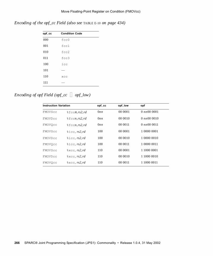
Move Floating-Point Register on Condition (FMOVcc)
Encoding of the opf_cc Field (also see TABLE E-10 on page 434)
Encoding of opf Field (opf_cc opf_low)
opf_cc Condition Code
000 fcc0
001 fcc1
010 fcc2
011 fcc3
100 icc
101 —
110 xcc
111 —
Instruction Variation opf_cc opf_low opf
FMOVScc %fccn,rs2,rd 0nn 00 0001 0 nn00 0001
FMOVDcc %fccn,rs2,rd 0nn 00 0010 0 nn00 0010
FMOVQcc %fccn,rs2,rd 0nn 00 0011 0 nn00 0011
FMOVScc %icc, rs2,rd 100 00 0001 1 0000 0001
FMOVDcc %icc, rs2,rd 100 00 0010 1 0000 0010
FMOVQcc %icc, rs2,rd 100 00 0011 1 0000 0011
FMOVScc %xcc, rs2,rd 110 00 0001 1 1000 0001
FMOVDcc %xcc, rs2,rd 110 00 0010 1 1000 0010
FMOVQcc %xcc, rs2,rd 110 00 0011 1 1000 0011
266 SPARC® Joint Programming Specification (JPS1): Commonality • Release 1.0.4, 31 May 2002
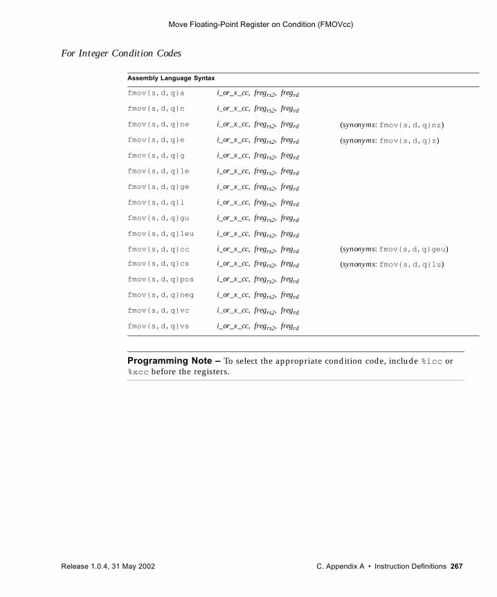
Move Floating-Point Register on Condition (FMOVcc)
For Integer Condition Codes
Programming Note – To select the appropriate condition code, include %icc or %xcc before the registers.
Assembly Language Syntax
fmov{s,d,q}a i_or_x_cc, fregrs2, fregrd
fmov{s,d,q}n i_or_x_cc, fregrs2, fregrd
fmov{s,d,q}ne i_or_x_cc, fregrs2, fregrd (synonyms: fmov{s,d,q}nz)
fmov{s,d,q}e i_or_x_cc, fregrs2, fregrd (synonyms: fmov{s,d,q}z)
fmov{s,d,q}g i_or_x_cc, fregrs2, fregrd
fmov{s,d,q}le i_or_x_cc, fregrs2, fregrd
fmov{s,d,q}ge i_or_x_cc, fregrs2, fregrd
fmov{s,d,q}l i_or_x_cc, fregrs2, fregrd
fmov{s,d,q}gu i_or_x_cc, fregrs2, fregrd
fmov{s,d,q}leu i_or_x_cc, fregrs2, fregrd
fmov{s,d,q}cc i_or_x_cc, fregrs2, fregrd (synonyms: fmov{s,d,q}geu)
fmov{s,d,q}cs i_or_x_cc, fregrs2, fregrd (synonyms: fmov{s,d,q}lu)
fmov{s,d,q}pos i_or_x_cc, fregrs2, fregrd
fmov{s,d,q}neg i_or_x_cc, fregrs2, fregrd
fmov{s,d,q}vc i_or_x_cc, fregrs2, fregrd
fmov{s,d,q}vs i_or_x_cc, fregrs2, fregrd
Release 1.0.4, 31 May 2002 C. Appendix A • Instruction Definitions 267
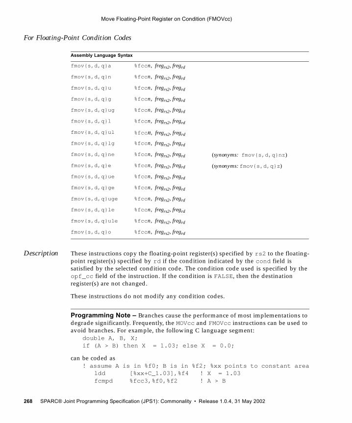
Move Floating-Point Register on Condition (FMOVcc)
For Floating-Point Condition Codes
Description These instructions copy the floating-point register(s) specified by rs2 to the floating-point register(s) specified by rd if the condition indicated by the cond field is satisfied by the selected condition code. The condition code used is specified by the opf_cc field of the instruction. If the condition is FALSE, then the destination register(s) are not changed.
These instructions do not modify any condition codes.
Programming Note – Branches cause the performance of most implementations to degrade significantly. Frequently, the MOVcc and FMOVcc instructions can be used to avoid branches. For example, the following C language segment:
double A, B, X;if (A > B) then X = 1.03; else X = 0.0;
can be coded as! assume A is in %f0; B is in %f2; %xx points to constant area
ldd [%xx+C_1.03],%f4 ! X = 1.03fcmpd %fcc3,%f0,%f2 ! A > B
Assembly Language Syntax
fmov{s,d,q}a %fccn, fregrs2, fregrd
fmov{s,d,q}n %fccn, fregrs2, fregrd
fmov{s,d,q}u %fccn, fregrs2, fregrd
fmov{s,d,q}g %fccn, fregrs2, fregrd
fmov{s,d,q}ug %fccn, fregrs2, fregrd
fmov{s,d,q}l %fccn, fregrs2, fregrd
fmov{s,d,q}ul %fccn, fregrs2, fregrd
fmov{s,d,q}lg %fccn, fregrs2, fregrd
fmov{s,d,q}ne %fccn, fregrs2, fregrd (synonyms: fmov{s,d,q}nz)
fmov{s,d,q}e %fccn, fregrs2, fregrd (synonyms: fmov{s,d,q}z)
fmov{s,d,q}ue %fccn, fregrs2, fregrd
fmov{s,d,q}ge %fccn, fregrs2, fregrd
fmov{s,d,q}uge %fccn, fregrs2, fregrd
fmov{s,d,q}le %fccn, fregrs2, fregrd
fmov{s,d,q}ule %fccn, fregrs2, fregrd
fmov{s,d,q}o %fccn, fregrs2, fregrd
268 SPARC® Joint Programming Specification (JPS1): Commonality • Release 1.0.4, 31 May 2002
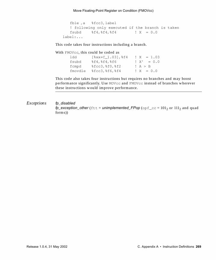
Move Floating-Point Register on Condition (FMOVcc)
fble ,a %fcc3,label! following only executed if the branch is takenfsubd %f4,%f4,%f4 ! X = 0.0
label:...
This code takes four instructions including a branch.
With FMOVcc, this could be coded asldd [%xx+C_1.03],%f4 ! X = 1.03fsubd %f4,%f4,%f6 ! X’ = 0.0 fcmpd %fcc3,%f0,%f2 ! A > Bfmovdle %fcc3,%f6,%f4 ! X = 0.0
This code also takes four instructions but requires no branches and may boost performance significantly. Use MOVcc and FMOVcc instead of branches wherever these instructions would improve performance.
Exceptions fp_disabledfp_exception_other (ftt = unimplemented_FPop (opf_cc = 1012 or 1112 and quad forms))
Release 1.0.4, 31 May 2002 C. Appendix A • Instruction Definitions 269
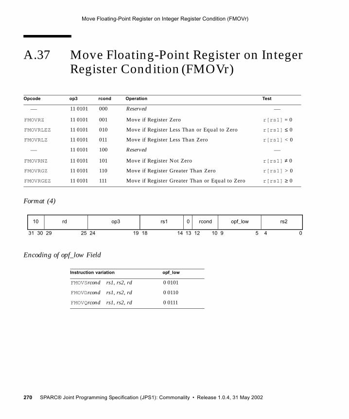
Move Floating-Point Register on Integer Register Condition (FMOVr)
A.37 Move Floating-Point Register on Integer Register Condition (FMOVr)
Format (4)
Encoding of opf_low Field
Opcode op3 rcond Operation Test
— 11 0101 000 Reserved —
FMOVRZ 11 0101 001 Move if Register Zero r[rs1] = 0
FMOVRLEZ 11 0101 010 Move if Register Less Than or Equal to Zero r[rs1] ≤ 0
FMOVRLZ 11 0101 011 Move if Register Less Than Zero r[rs1] < 0
— 11 0101 100 Reserved —
FMOVRNZ 11 0101 101 Move if Register Not Zero r[rs1] ≠ 0
FMOVRGZ 11 0101 110 Move if Register Greater Than Zero r[rs1] > 0
FMOVRGEZ 11 0101 111 Move if Register Greater Than or Equal to Zero r[rs1] ≥ 0
Instruction variation opf_low
FMOVSrcond rs1, rs2, rd 0 0101
FMOVDrcond rs1, rs2, rd 0 0110
FMOVQrcond rs1, rs2, rd 0 0111
31 141924 18 13 12 9 5 4 0102530 29
10 rd op3 0 rcond opf_low rs2rs1
270 SPARC® Joint Programming Specification (JPS1): Commonality • Release 1.0.4, 31 May 2002
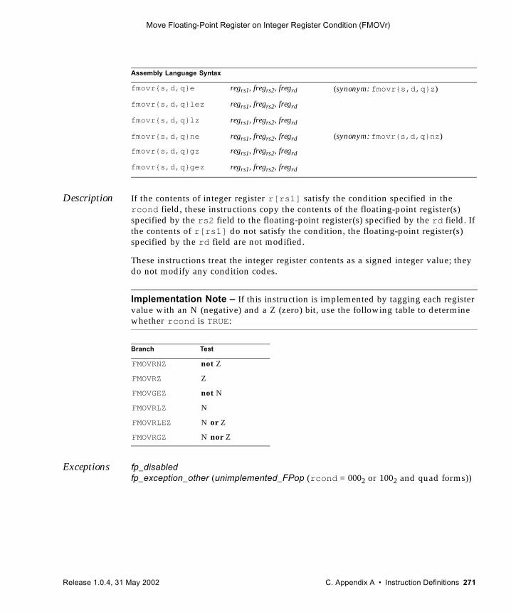
Move Floating-Point Register on Integer Register Condition (FMOVr)
Description If the contents of integer register r[rs1] satisfy the condition specified in the rcond field, these instructions copy the contents of the floating-point register(s) specified by the rs2 field to the floating-point register(s) specified by the rd field. If the contents of r[rs1] do not satisfy the condition, the floating-point register(s) specified by the rd field are not modified.
These instructions treat the integer register contents as a signed integer value; they do not modify any condition codes.
Implementation Note – If this instruction is implemented by tagging each register value with an N (negative) and a Z (zero) bit, use the following table to determine whether rcond is TRUE:
Exceptions fp_disabledfp_exception_other (unimplemented_FPop (rcond = 0002 or 1002 and quad forms))
Assembly Language Syntax
fmovr{s,d,q}e regrs1, fregrs2, fregrd (synonym: fmovr{s,d,q}z)
fmovr{s,d,q}lez regrs1, fregrs2, fregrd
fmovr{s,d,q}lz regrs1, fregrs2, fregrd
fmovr{s,d,q}ne regrs1, fregrs2, fregrd (synonym: fmovr{s,d,q}nz)
fmovr{s,d,q}gz regrs1, fregrs2, fregrd
fmovr{s,d,q}gez regrs1, fregrs2, fregrd
Branch Test
FMOVRNZ not Z
FMOVRZ Z
FMOVGEZ not N
FMOVRLZ N
FMOVRLEZ N or Z
FMOVRGZ N nor Z
Release 1.0.4, 31 May 2002 C. Appendix A • Instruction Definitions 271
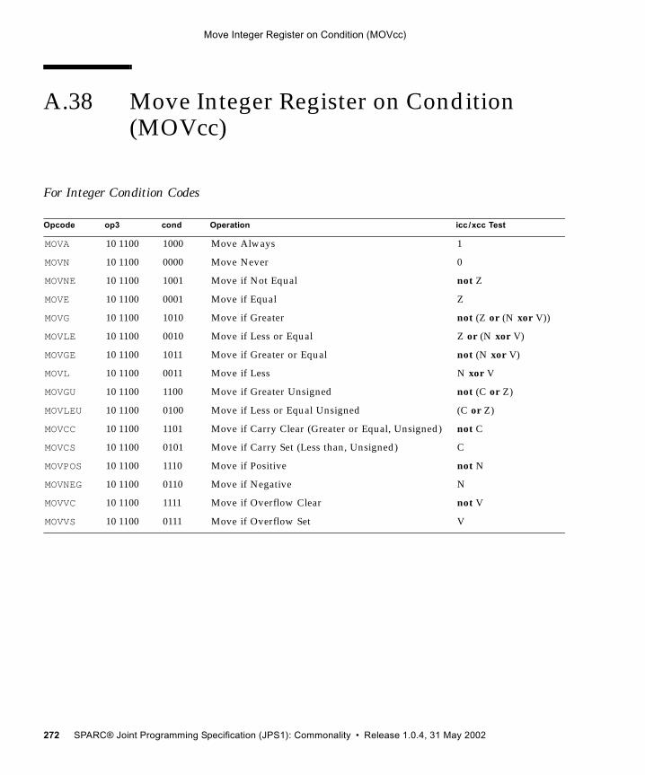
Move Integer Register on Condition (MOVcc)
A.38 Move Integer Register on Condition (MOVcc)
For Integer Condition Codes
Opcode op3 cond Operation icc/xcc Test
MOVA 10 1100 1000 Move Always 1
MOVN 10 1100 0000 Move Never 0
MOVNE 10 1100 1001 Move if Not Equal not Z
MOVE 10 1100 0001 Move if Equal Z
MOVG 10 1100 1010 Move if Greater not (Z or (N xor V))
MOVLE 10 1100 0010 Move if Less or Equal Z or (N xor V)
MOVGE 10 1100 1011 Move if Greater or Equal not (N xor V)
MOVL 10 1100 0011 Move if Less N xor V
MOVGU 10 1100 1100 Move if Greater Unsigned not (C or Z)
MOVLEU 10 1100 0100 Move if Less or Equal Unsigned (C or Z)
MOVCC 10 1100 1101 Move if Carry Clear (Greater or Equal, Unsigned) not C
MOVCS 10 1100 0101 Move if Carry Set (Less than, Unsigned) C
MOVPOS 10 1100 1110 Move if Positive not N
MOVNEG 10 1100 0110 Move if Negative N
MOVVC 10 1100 1111 Move if Overflow Clear not V
MOVVS 10 1100 0111 Move if Overflow Set V
272 SPARC® Joint Programming Specification (JPS1): Commonality • Release 1.0.4, 31 May 2002
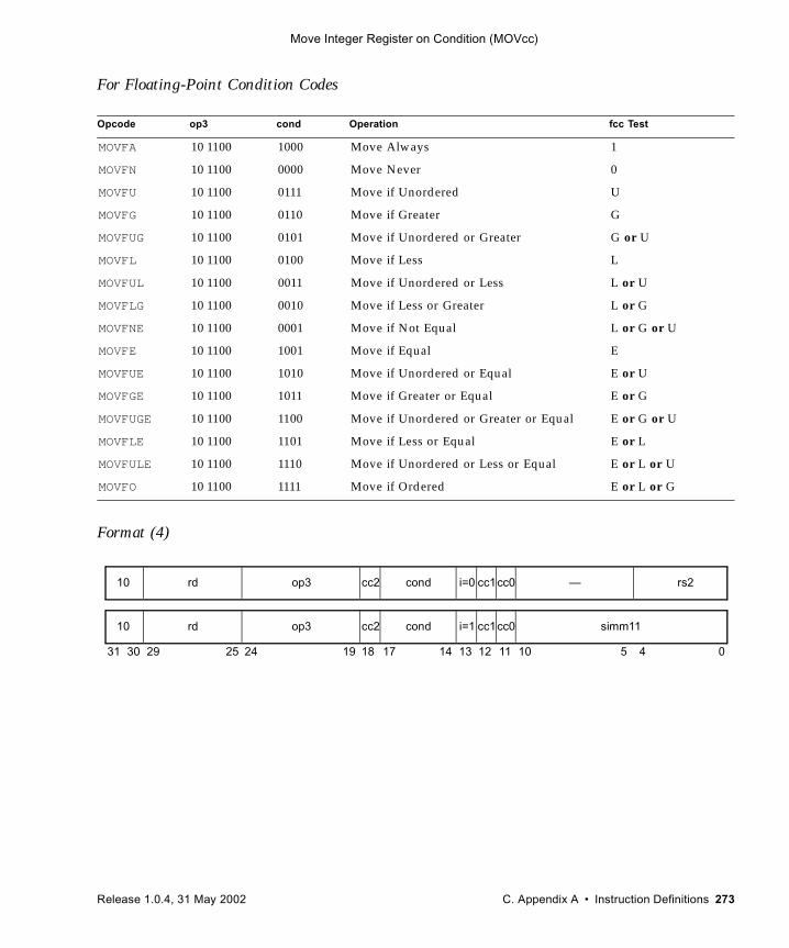
Move Integer Register on Condition (MOVcc)
For Floating-Point Condition Codes
Format (4)
Opcode op3 cond Operation fcc Test
MOVFA 10 1100 1000 Move Always 1
MOVFN 10 1100 0000 Move Never 0
MOVFU 10 1100 0111 Move if Unordered U
MOVFG 10 1100 0110 Move if Greater G
MOVFUG 10 1100 0101 Move if Unordered or Greater G or U
MOVFL 10 1100 0100 Move if Less L
MOVFUL 10 1100 0011 Move if Unordered or Less L or U
MOVFLG 10 1100 0010 Move if Less or Greater L or G
MOVFNE 10 1100 0001 Move if Not Equal L or G or U
MOVFE 10 1100 1001 Move if Equal E
MOVFUE 10 1100 1010 Move if Unordered or Equal E or U
MOVFGE 10 1100 1011 Move if Greater or Equal E or G
MOVFUGE 10 1100 1100 Move if Unordered or Greater or Equal E or G or U
MOVFLE 10 1100 1101 Move if Less or Equal E or L
MOVFULE 10 1100 1110 Move if Unordered or Less or Equal E or L or U
MOVFO 10 1100 1111 Move if Ordered E or L or G
31 24 02530 29 19 18
rd10 op3 —
14 13 12 5 4
cond rs2i=0
rd10 op3 cond simm11i=1
17
cc2
cc2
11
cc1
cc1
10
cc0
cc0
Release 1.0.4, 31 May 2002 C. Appendix A • Instruction Definitions 273
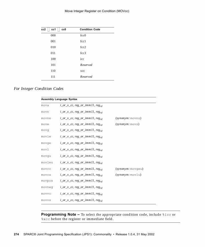
Move Integer Register on Condition (MOVcc)
For Integer Condition Codes
Programming Note – To select the appropriate condition code, include %icc or %xcc before the register or immediate field.
cc2 cc1 cc0 Condition Code
000 fcc0
001 fcc1
010 fcc2
011 fcc3
100 icc
101 Reserved
110 xcc
111 Reserved
Assembly Language Syntax
mova i_or_x_cc, reg_or_imm11, regrd
movn i_or_x_cc, reg_or_imm11, regrd
movne i_or_x_cc, reg_or_imm11, regrd (synonym: movnz)
move i_or_x_cc, reg_or_imm11, regrd (synonym: movz)
movg i_or_x_cc, reg_or_imm11, regrd
movle i_or_x_cc, reg_or_imm11, regrd
movge i_or_x_cc, reg_or_imm11, regrd
movl i_or_x_cc, reg_or_imm11, regrd
movgu i_or_x_cc, reg_or_imm11, regrd
movleu i_or_x_cc, reg_or_imm11, regrd
movcc i_or_x_cc, reg_or_imm11, regrd (synonym: movgeu)
movcs i_or_x_cc, reg_or_imm11, regrd (synonym: movlu)
movpos i_or_x_cc, reg_or_imm11, regrd
movneg i_or_x_cc, reg_or_imm11, regrd
movvc i_or_x_cc, reg_or_imm11, regrd
movvs i_or_x_cc, reg_or_imm11, regrd
274 SPARC® Joint Programming Specification (JPS1): Commonality • Release 1.0.4, 31 May 2002
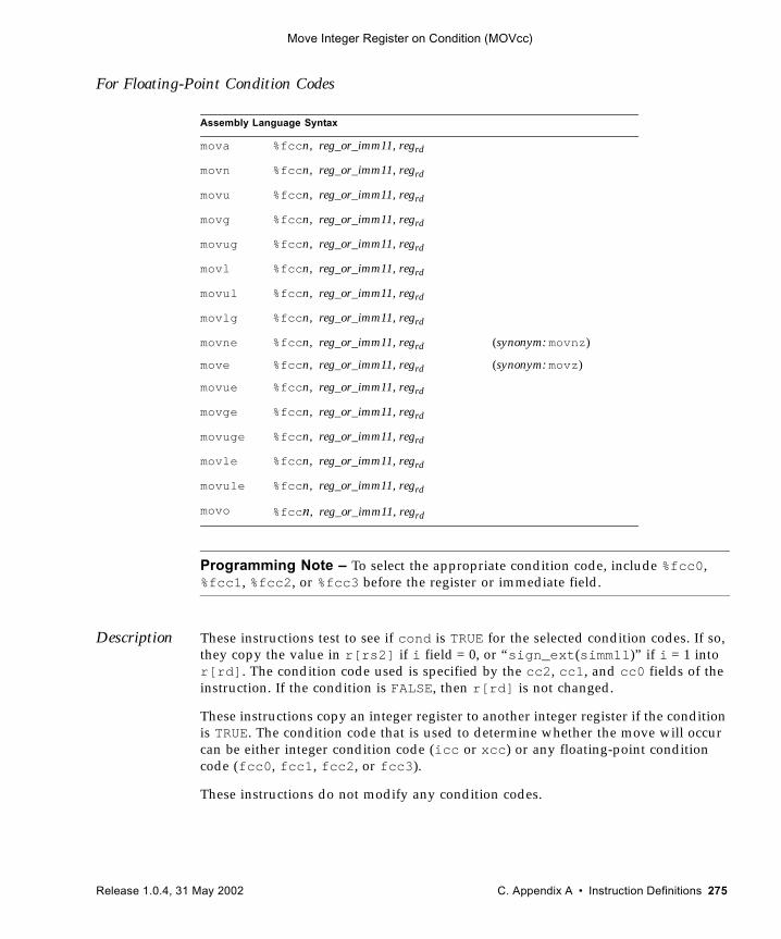
Move Integer Register on Condition (MOVcc)
For Floating-Point Condition Codes
Programming Note – To select the appropriate condition code, include %fcc0, %fcc1, %fcc2, or %fcc3 before the register or immediate field.
Description These instructions test to see if cond is TRUE for the selected condition codes. If so, they copy the value in r[rs2] if i field = 0, or “sign_ext(simm11)” if i = 1 into r[rd]. The condition code used is specified by the cc2, cc1, and cc0 fields of the instruction. If the condition is FALSE, then r[rd] is not changed.
These instructions copy an integer register to another integer register if the condition is TRUE. The condition code that is used to determine whether the move will occur can be either integer condition code (icc or xcc) or any floating-point condition code (fcc0, fcc1, fcc2, or fcc3).
These instructions do not modify any condition codes.
Assembly Language Syntax
mova %fccn, reg_or_imm11, regrd
movn %fccn, reg_or_imm11, regrd
movu %fccn, reg_or_imm11, regrd
movg %fccn, reg_or_imm11, regrd
movug %fccn, reg_or_imm11, regrd
movl %fccn, reg_or_imm11, regrd
movul %fccn, reg_or_imm11, regrd
movlg %fccn, reg_or_imm11, regrd
movne %fccn, reg_or_imm11, regrd (synonym: movnz)
move %fccn, reg_or_imm11, regrd (synonym: movz)
movue %fccn, reg_or_imm11, regrd
movge %fccn, reg_or_imm11, regrd
movuge %fccn, reg_or_imm11, regrd
movle %fccn, reg_or_imm11, regrd
movule %fccn, reg_or_imm11, regrd
movo %fccn, reg_or_imm11, regrd
Release 1.0.4, 31 May 2002 C. Appendix A • Instruction Definitions 275
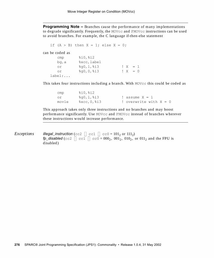
Move Integer Register on Condition (MOVcc)
Programming Note – Branches cause the performance of many implementations to degrade significantly. Frequently, the MOVcc and FMOVcc instructions can be used to avoid branches. For example, the C language if-then-else statement
if (A > B) then X = 1; else X = 0;
can be coded ascmp %i0,%i2bg,a %xcc,labelor %g0,1,%i3 ! X = 1or %g0,0,%i3 ! X = 0
label:...
This takes four instructions including a branch. With MOVcc this could be coded as
cmp %i0,%i2or %g0,1,%i3 ! assume X = 1movle %xcc,0,%i3 ! overwrite with X = 0
This approach takes only three instructions and no branches and may boost performance significantly. Use MOVcc and FMOVcc instead of branches wherever these instructions would increase performance.
Exceptions illegal_instruction (cc2 cc1 cc0 = 1012 or 1112)fp_disabled (cc2 cc1 cc0 = 0002 , 0012, 0102 , or 0112 and the FPU is disabled)
276 SPARC® Joint Programming Specification (JPS1): Commonality • Release 1.0.4, 31 May 2002
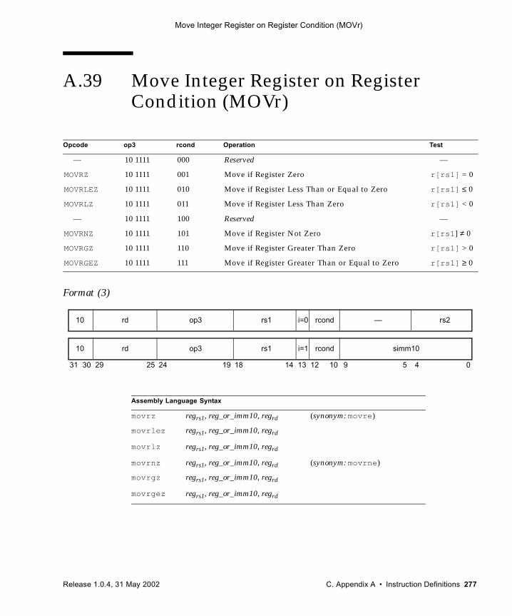
Move Integer Register on Register Condition (MOVr)
A.39 Move Integer Register on Register Condition (MOVr)
Format (3)
Opcode op3 rcond Operation Test
— 10 1111 000 Reserved —
MOVRZ 10 1111 001 Move if Register Zero r[rs1] = 0
MOVRLEZ 10 1111 010 Move if Register Less Than or Equal to Zero r[rs1] ≤ 0
MOVRLZ 10 1111 011 Move if Register Less Than Zero r[rs1] < 0
— 10 1111 100 Reserved —
MOVRNZ 10 1111 101 Move if Register Not Zero r[rs1] ≠ 0
MOVRGZ 10 1111 110 Move if Register Greater Than Zero r[rs1] > 0
MOVRGEZ 10 1111 111 Move if Register Greater Than or Equal to Zero r[rs1] ≥ 0
Assembly Language Syntax
movrz regrs1, reg_or_imm10, regrd (synonym: movre)
movrlez regrs1, reg_or_imm10, regrd
movrlz regrs1, reg_or_imm10, regrd
movrnz regrs1, reg_or_imm10, regrd (synonym: movrne)
movrgz regrs1, reg_or_imm10, regrd
movrgez regrs1, reg_or_imm10, regrd
31 24 02530 29 19 18
rd10 op3 —
14 13 12 5 4
rs1 rs2i=0
rd10 op3 rs1 simm10i=1
rcond
rcond
10 9
Release 1.0.4, 31 May 2002 C. Appendix A • Instruction Definitions 277
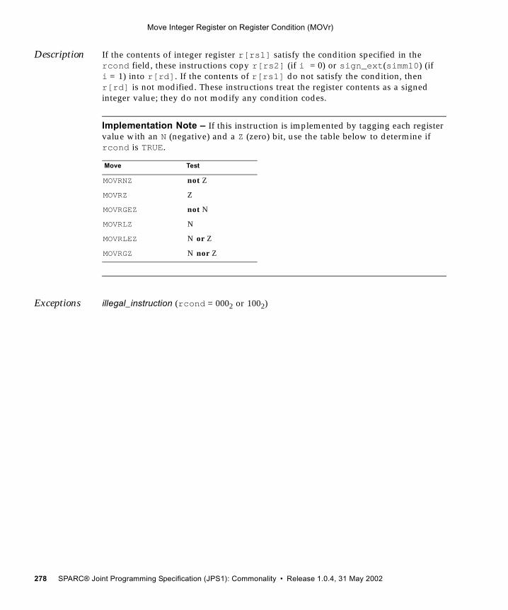
Move Integer Register on Register Condition (MOVr)
Description If the contents of integer register r[rs1] satisfy the condition specified in the rcond field, these instructions copy r[rs2] (if i = 0) or sign_ext(simm10) (if i = 1) into r[rd]. If the contents of r[rs1] do not satisfy the condition, then r[rd] is not modified. These instructions treat the register contents as a signed integer value; they do not modify any condition codes.
Implementation Note – If this instruction is implemented by tagging each register value with an N (negative) and a Z (zero) bit, use the table below to determine if rcond is TRUE.
Exceptions illegal_instruction (rcond = 0002 or 1002)
Move Test
MOVRNZ not Z
MOVRZ Z
MOVRGEZ not N
MOVRLZ N
MOVRLEZ N or Z
MOVRGZ N nor Z
278 SPARC® Joint Programming Specification (JPS1): Commonality • Release 1.0.4, 31 May 2002
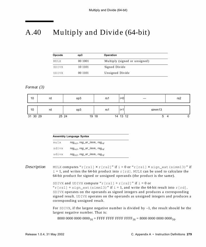
Multiply and Divide (64-bit)
A.40 Multiply and Divide (64-bit)
Format (3)
Description MULX computes “r[rs1] × r[rs2]” if i = 0 or “r[rs1] × sign_ext(simm13)” if i = 1, and writes the 64-bit product into r[rd]. MULX can be used to calculate the 64-bit product for signed or unsigned operands (the product is the same).
SDIVX and UDIVX compute “r[rs1] ÷ r[rs2]” if i = 0 or “r[rs1] ÷ sign_ext(simm13)” if i = 1, and write the 64-bit result into r[rd]. SDIVX operates on the operands as signed integers and produces a corresponding signed result. UDIVX operates on the operands as unsigned integers and produces a corresponding unsigned result.
For SDIVX, if the largest negative number is divided by –1, the result should be the largest negative number. That is:
8000 0000 0000 000016 ÷ FFFF FFFF FFFF FFFF16 = 8000 0000 0000 000016.
Opcode op3 Operation
MULX 00 1001 Multiply (signed or unsigned)
SDIVX 10 1101 Signed Divide
UDIVX 00 1101 Unsigned Divide
Assembly Language Syntax
mulx regrs1, reg_or_imm, regrd
sdivx regrs1, reg_or_imm, regrd
udivx regrs1, reg_or_imm, regrd
31 24 02530 29 19 18
rd10 op3 —
14 13 12 5 4
rs1 rs2i=0
rd10 op3 rs1 simm13i=1
Release 1.0.4, 31 May 2002 C. Appendix A • Instruction Definitions 279
Multiply and Divide (64-bit)
These instructions do not modify any condition codes.
Exceptions division_by_zero
280 SPARC® Joint Programming Specification (JPS1): Commonality • Release 1.0.4, 31 May 2002
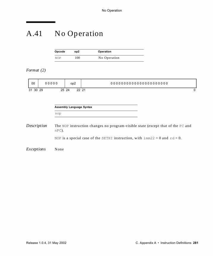
No Operation
A.41 No Operation
Format (2)
Description The NOP instruction changes no program-visible state (except that of the PC and nPC).
NOP is a special case of the SETHI instruction, with imm22 = 0 and rd = 0.
Exceptions None
Opcode op2 Operation
NOP 100 No Operation
Assembly Language Syntax
nop
31 24 02530 29 22 21
00 op2 0 0 0 0 0 0 0 0 0 0 0 0 0 0 0 0 0 0 0 0 0 00 0 0 0 0
Release 1.0.4, 31 May 2002 C. Appendix A • Instruction Definitions 281
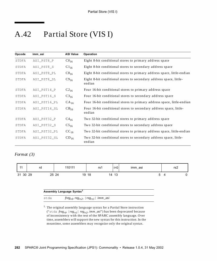
Partial Store (VIS I)
A.42 Partial Store (VIS I)
Format (3)
Opcode imm_asi ASI Value Operation
STDFA ASI_PST8_P C016 Eight 8-bit conditional stores to primary address space
STDFA ASI_PST8_S C116 Eight 8-bit conditional stores to secondary address space
STDFA ASI_PST8_PL C816 Eight 8-bit conditional stores to primary address space, little-endian
STDFA ASI_PST8_SL C916 Eight 8-bit conditional stores to secondary address space, little-endian
STDFA ASI_PST16_P C216 Four 16-bit conditional stores to primary address space
STDFA ASI_PST16_S C316 Four 16-bit conditional stores to secondary address space
STDFA ASI_PST16_PL CA16 Four 16-bit conditional stores to primary address space, little-endian
STDFA ASI_PST16_SL CB16 Four 16-bit conditional stores to secondary address space, little-endian
STDFA ASI_PST32_P C416 Two 32-bit conditional stores to primary address space
STDFA ASI_PST32_S C516 Two 32-bit conditional stores to secondary address space
STDFA ASI_PST32_PL CC16 Two 32-bit conditional stores to primary address space, little-endian
STDFA ASI_PST32_SL CD16 Two 32-bit conditional stores to secondary address space, little-endian
Assembly Language Syntax1
1. The original assembly language syntax for a Partial Store instruction (“stda fregrd, [regrs1] regrs2, imm_asi”) has been deprecated because of inconsistency with the rest of the SPARC assembly language. Over time, assemblers will support the new syntax for this instruction. In the meantime, some assemblers may recognize only the original syntax.
stda fregrd, regrs2, [regrs1] imm_asi
31 24 02530 29 19 18 14 13 5 4
rd11 110111 imm_asirs1 rs2i=0
282 SPARC® Joint Programming Specification (JPS1): Commonality • Release 1.0.4, 31 May 2002
Partial Store (VIS I)
Description The partial store instructions are selected by one of the partial store ASIs with the STDFA instruction.
Two 32-bit, four 16-bit, or eight 8-bit values from the 64-bit floating-point register specified by rd are conditionally stored at the address specified by r[rs1], using the mask specified in r[rs2]. The value in r[rs2] has the same format as the result specified by the pixel compare instructions (see Pixel Compare (VIS I) on page 292). The most significant bit of the mask (not the entire register) corresponds to the most significant part of the floating-point register specified by rd. The data is stored in little-endian form in memory if the ASI name has an “L” suffix; otherwise, it is stored in big-endian format.
A Partial Store instruction can cause a virtual (or physical) watchpoint exception when the following conditions are met: ■ The virtual (physical) address in r[rs1] matches the address in the VA (PA)
Data Watchpoint Register .
■ The byte store mask in r[rs2] indicates that a byte is to be stored.
■ The Virtual (Physical) Data Watchpoint Mask in DCUCR indicates that one or more of the bytes to be stored at the watched address is being watched.
IMPL. DEP. #249: For a Partial Store instruction, the following aspects of data watchpoints are implementation dependent: (a) whether data watchpoint logic examines the byte store mask in r[rs2] or it conservatively behaves as if every Partial Store always stores all 8 bytes, and (b) whether data watchpoint logic examines individual bits in the Virtual (Physical) Data Watchpoint Mask in DCUCR to determine which bytes are being watched or (when the Watchpoint Mask is nonzero) it conservatively behaves as if all 8 bytes are being watched.
ASIs C016-C516 and C816-CD16 are only used for partial store operations. In particular, they should not be used with the LDDFA instruction. See Partial Store ASIs on page 548 for more information.
Exceptions fp_disabledillegal_instruction (when i = 1: no immediate mode is supported.)PA_watchpoint (see text)VA_watchpoint (see text)mem_address_not_aligneddata_access_exceptiondata_access_errorfast_data_access_MMU_missfast_data_access_protection
Release 1.0.4, 31 May 2002 C. Appendix A • Instruction Definitions 283
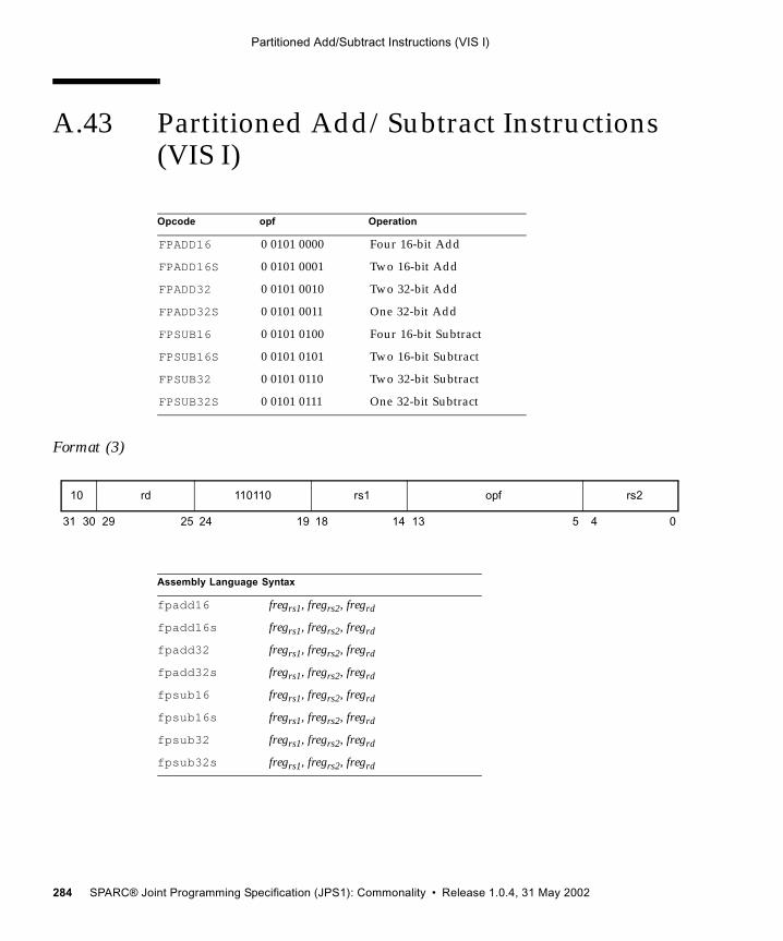
Partitioned Add/Subtract Instructions (VIS I)
A.43 Partitioned Add/Subtract Instructions (VIS I)
Format (3)
Opcode opf Operation
FPADD16 0 0101 0000 Four 16-bit Add
FPADD16S 0 0101 0001 Two 16-bit Add
FPADD32 0 0101 0010 Two 32-bit Add
FPADD32S 0 0101 0011 One 32-bit Add
FPSUB16 0 0101 0100 Four 16-bit Subtract
FPSUB16S 0 0101 0101 Two 16-bit Subtract
FPSUB32 0 0101 0110 Two 32-bit Subtract
FPSUB32S 0 0101 0111 One 32-bit Subtract
Assembly Language Syntax
fpadd16 fregrs1, fregrs2, fregrd
fpadd16s fregrs1, fregrs2, fregrd
fpadd32 fregrs1, fregrs2, fregrd
fpadd32s fregrs1, fregrs2, fregrd
fpsub16 fregrs1, fregrs2, fregrd
fpsub16s fregrs1, fregrs2, fregrd
fpsub32 fregrs1, fregrs2, fregrd
fpsub32s fregrs1, fregrs2, fregrd
31 24 02530 29 19 18 14 13 5 4
rd10 110110 opfrs1 rs2
284 SPARC® Joint Programming Specification (JPS1): Commonality • Release 1.0.4, 31 May 2002
Partitioned Add/Subtract Instructions (VIS I)
Description The standard versions of these instructions perform four 16-bit or two 32-bit partitioned adds or subtracts between the corresponding fixed-point values contained in the source operands (the 64-bit floating-point registers specified by rs1 and rs2). For subtraction, the second operand is subtracted from the first operand. The result is placed in the 64-bit destination register specified by rd.
The single-precision versions of these instructions (FPADD16S, FPSUB16S, FPADD32S, FPSUB32S) perform two 16-bit or one 32-bit partitioned add(s) or subtract(s); only the low 32-bits of the destination register are affected.
Exceptions fp_disabled
Release 1.0.4, 31 May 2002 C. Appendix A • Instruction Definitions 285
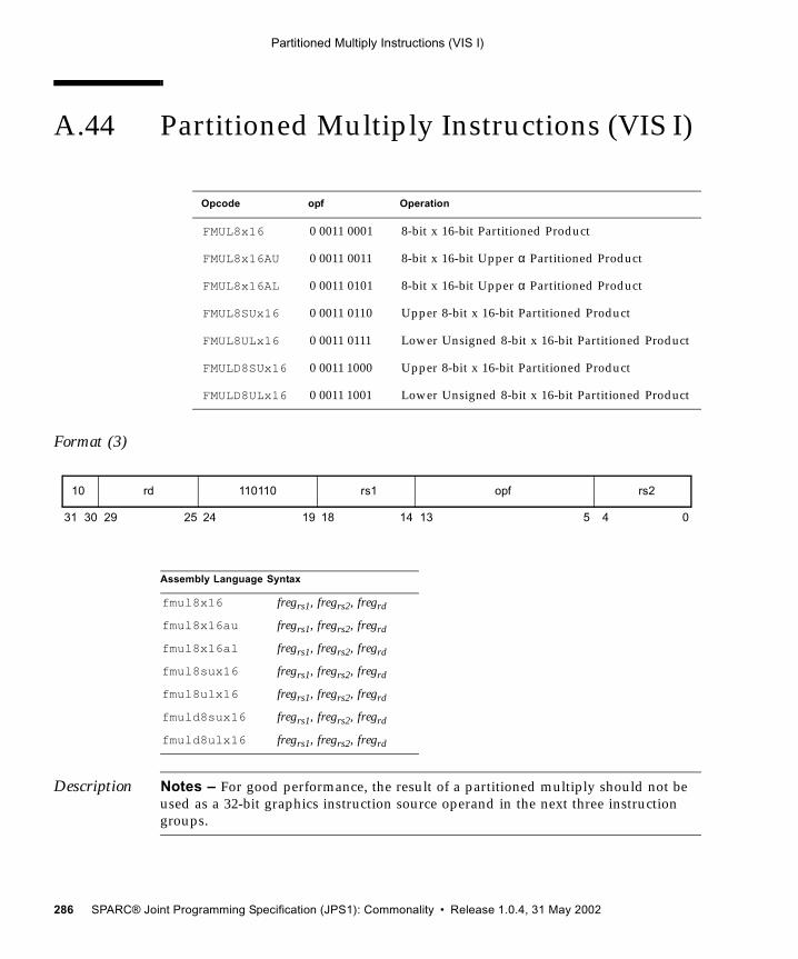
Partitioned Multiply Instructions (VIS I)
A.44 Partitioned Multiply Instructions (VIS I)
Format (3)
Description Notes – For good performance, the result of a partitioned multiply should not be used as a 32-bit graphics instruction source operand in the next three instruction groups.
Opcode opf Operation
FMUL8x16 0 0011 0001 8-bit x 16-bit Partitioned Product
FMUL8x16AU 0 0011 0011 8-bit x 16-bit Upper α Partitioned Product
FMUL8x16AL 0 0011 0101 8-bit x 16-bit Upper α Partitioned Product
FMUL8SUx16 0 0011 0110 Upper 8-bit x 16-bit Partitioned Product
FMUL8ULx16 0 0011 0111 Lower Unsigned 8-bit x 16-bit Partitioned Product
FMULD8SUx16 0 0011 1000 Upper 8-bit x 16-bit Partitioned Product
FMULD8ULx16 0 0011 1001 Lower Unsigned 8-bit x 16-bit Partitioned Product
Assembly Language Syntax
fmul8x16 fregrs1, fregrs2, fregrd
fmul8x16au fregrs1, fregrs2, fregrd
fmul8x16al fregrs1, fregrs2, fregrd
fmul8sux16 fregrs1, fregrs2, fregrd
fmul8ulx16 fregrs1, fregrs2, fregrd
fmuld8sux16 fregrs1, fregrs2, fregrd
fmuld8ulx16 fregrs1, fregrs2, fregrd
31 24 02530 29 19 18 14 13 5 4
rd10 110110 opfrs1 rs2
286 SPARC® Joint Programming Specification (JPS1): Commonality • Release 1.0.4, 31 May 2002
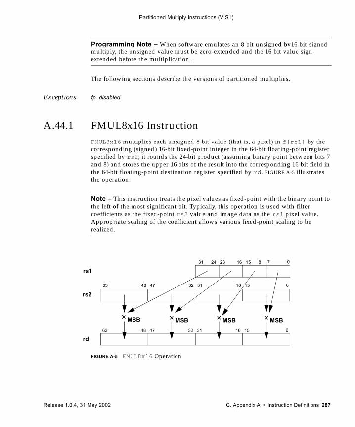
Partitioned Multiply Instructions (VIS I)
Programming Note – When software emulates an 8-bit unsigned by16-bit signed multiply, the unsigned value must be zero-extended and the 16-bit value sign-extended before the multiplication.
The following sections describe the versions of partitioned multiplies.
Exceptions fp_disabled
A.44.1 FMUL8x16 InstructionFMUL8x16 multiplies each unsigned 8-bit value (that is, a pixel) in f[rs1] by the corresponding (signed) 16-bit fixed-point integer in the 64-bit floating-point register specified by rs2; it rounds the 24-bit product (assuming binary point between bits 7 and 8) and stores the upper 16 bits of the result into the corresponding 16-bit field in the 64-bit floating-point destination register specified by rd. FIGURE A-5 illustrates the operation.
Note – This instruction treats the pixel values as fixed-point with the binary point to the left of the most significant bit. Typically, this operation is used with filter coefficients as the fixed-point rs2 value and image data as the rs1 pixel value. Appropriate scaling of the coefficient allows various fixed-point scaling to be realized.
FIGURE A-5 FMUL8x16 Operation
0151631
rs1
rd
24 23 8 7
rs2
015163132474863
015163132474863
× MSB × MSB × MSB × MSB
Release 1.0.4, 31 May 2002 C. Appendix A • Instruction Definitions 287
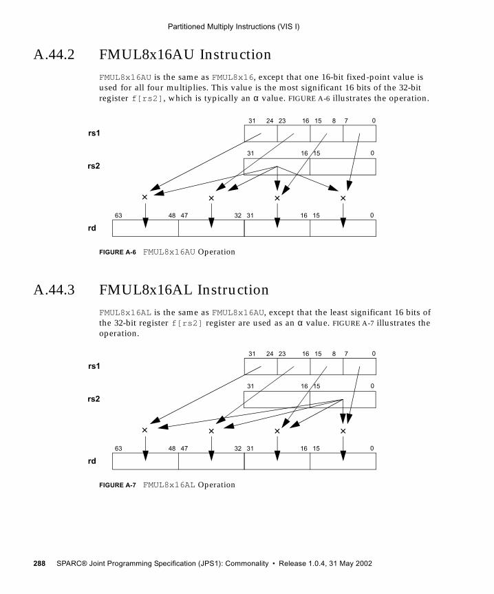
Partitioned Multiply Instructions (VIS I)
A.44.2 FMUL8x16AU InstructionFMUL8x16AU is the same as FMUL8x16, except that one 16-bit fixed-point value is used for all four multiplies. This value is the most significant 16 bits of the 32-bit register f[rs2], which is typically an α value. FIGURE A-6 illustrates the operation.
FIGURE A-6 FMUL8x16AU Operation
A.44.3 FMUL8x16AL InstructionFMUL8x16AL is the same as FMUL8x16AU, except that the least significant 16 bits of the 32-bit register f[rs2] register are used as an α value. FIGURE A-7 illustrates the operation.
FIGURE A-7 FMUL8x16AL Operation
0151631
rs1
rd
24 23 8 7
rs2
0151631
015163132474863
× × × ×
0151631
rs1
rd
24 23 8 7
rs2
0151631
015163132474863
× × × ×
288 SPARC® Joint Programming Specification (JPS1): Commonality • Release 1.0.4, 31 May 2002
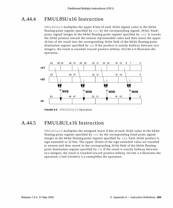
Partitioned Multiply Instructions (VIS I)
A.44.4 FMUL8SUx16 InstructionFMUL8SUx16 multiplies the upper 8 bits of each 16-bit signed value in the 64-bit floating-point register specified by rs1 by the corresponding signed, 16-bit, fixed-point, signed integer in the 64-bit floating-point register specified by rs2. It rounds the 24-bit product toward the nearest representable value and then stores the upper 16 bits of the result into the corresponding 16-bit field of the 64-bit floating-point destination register specified by rd. If the product is exactly halfway between two integers, the result is rounded toward positive infinity. FIGURE A-8 illustrates the operation.
FIGURE A-8 FMUL8SUx16 Operation
A.44.5 FMUL8ULx16 InstructionFMUL8ULx16 multiplies the unsigned lower 8 bits of each 16-bit value in the 64-bit floating-point register specified by rs1 by the corresponding fixed-point signed integer in the 64-bit floating-point register specified by rs2. Each 24-bit product is sign-extended to 32 bits. The upper 16-bits of the sign-extended value are rounded to nearest and then stored in the corresponding 16-bit field of the 64-bit floating-point destination register specified by rd. If the result is exactly halfway between two integers, the result is rounded toward positive infinity. FIGURE A-9 illustrates the operation; CODE EXAMPLE A-4 exemplifies the operation.
rs1
rd
rs2
015163132474863
× MSB × MSB × MSB × MSB
015163132474863
015163132474863 56 55 40 39 24 23 8 7
Release 1.0.4, 31 May 2002 C. Appendix A • Instruction Definitions 289
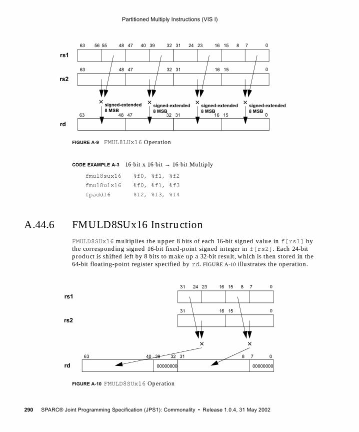
Partitioned Multiply Instructions (VIS I)
FIGURE A-9 FMUL8LUx16 Operation
A.44.6 FMULD8SUx16 InstructionFMULD8SUx16 multiplies the upper 8 bits of each 16-bit signed value in f[rs1] by the corresponding signed 16-bit fixed-point signed integer in f[rs2]. Each 24-bit product is shifted left by 8 bits to make up a 32-bit result, which is then stored in the 64-bit floating-point register specified by rd. FIGURE A-10 illustrates the operation.
FIGURE A-10 FMULD8SUx16 Operation
CODE EXAMPLE A-3 16-bit x 16-bit → 16-bit Multiply
fmul8sux16 %f0, %f1, %f2
fmul8ulx16 %f0, %f1, %f3
fpadd16 %f2, %f3, %f4
rs1
rd
rs2
015163132474863
× signed-extended × signed-extended × signed-extended × signed-extended
015163132474863
015163132474863 56 55 40 39 24 23 8 7
8 MSB 8 MSB 8 MSB 8 MSB
rs1
rd
rs2
0783132394063
× ×
0151631
0151631 24 23 8 7
0000000000000000
290 SPARC® Joint Programming Specification (JPS1): Commonality • Release 1.0.4, 31 May 2002
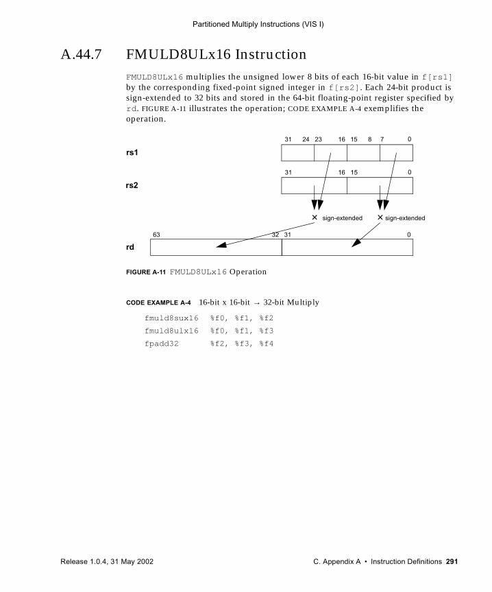
Partitioned Multiply Instructions (VIS I)
A.44.7 FMULD8ULx16 InstructionFMULD8ULx16 multiplies the unsigned lower 8 bits of each 16-bit value in f[rs1] by the corresponding fixed-point signed integer in f[rs2]. Each 24-bit product is sign-extended to 32 bits and stored in the 64-bit floating-point register specified by rd. FIGURE A-11 illustrates the operation; CODE EXAMPLE A-4 exemplifies the operation.
FIGURE A-11 FMULD8ULx16 Operation
CODE EXAMPLE A-4 16-bit x 16-bit → 32-bit Multiply
fmuld8sux16 %f0, %f1, %f2
fmuld8ulx16 %f0, %f1, %f3
fpadd32 %f2, %f3, %f4
rs1
rd
rs2
0313263
× ×
0151631
0151631 24 23 8 7
sign-extended sign-extended
Release 1.0.4, 31 May 2002 C. Appendix A • Instruction Definitions 291
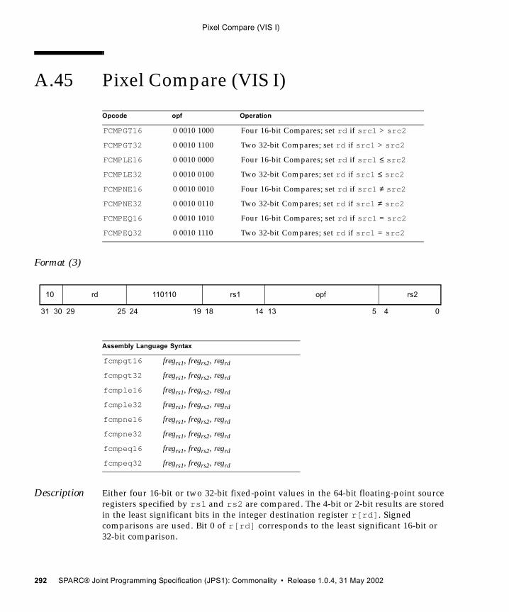
Pixel Compare (VIS I)
A.45 Pixel Compare (VIS I)
Format (3)
Description Either four 16-bit or two 32-bit fixed-point values in the 64-bit floating-point source registers specified by rs1 and rs2 are compared. The 4-bit or 2-bit results are stored in the least significant bits in the integer destination register r[rd]. Signed comparisons are used. Bit 0 of r[rd] corresponds to the least significant 16-bit or 32-bit comparison.
Opcode opf Operation
FCMPGT16 0 0010 1000 Four 16-bit Compares; set rd if src1 > src2
FCMPGT32 0 0010 1100 Two 32-bit Compares; set rd if src1 > src2
FCMPLE16 0 0010 0000 Four 16-bit Compares; set rd if src1 ≤ src2
FCMPLE32 0 0010 0100 Two 32-bit Compares; set rd if src1 ≤ src2
FCMPNE16 0 0010 0010 Four 16-bit Compares; set rd if src1 ≠ src2
FCMPNE32 0 0010 0110 Two 32-bit Compares; set rd if src1 ≠ src2
FCMPEQ16 0 0010 1010 Four 16-bit Compares; set rd if src1 = src2
FCMPEQ32 0 0010 1110 Two 32-bit Compares; set rd if src1 = src2
Assembly Language Syntax
fcmpgt16 fregrs1, fregrs2, regrd
fcmpgt32 fregrs1, fregrs2, regrd
fcmple16 fregrs1, fregrs2, regrd
fcmple32 fregrs1, fregrs2, regrd
fcmpne16 fregrs1, fregrs2, regrd
fcmpne32 fregrs1, fregrs2, regrd
fcmpeq16 fregrs1, fregrs2, regrd
fcmpeq32 fregrs1, fregrs2, regrd
31 24 02530 29 19 18 14 13 5 4
rd10 110110 opfrs1 rs2
292 SPARC® Joint Programming Specification (JPS1): Commonality • Release 1.0.4, 31 May 2002
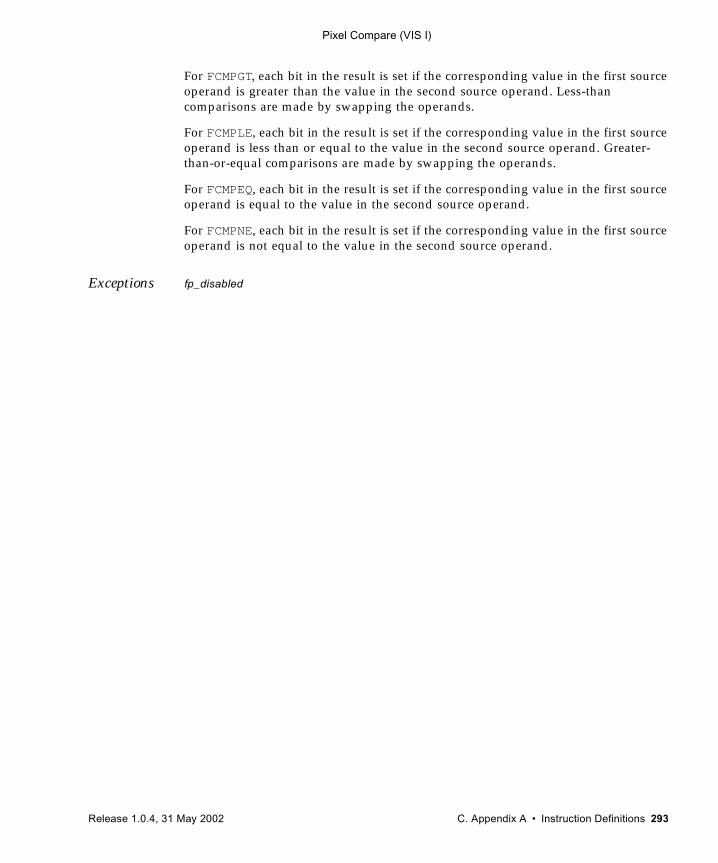
Pixel Compare (VIS I)
For FCMPGT, each bit in the result is set if the corresponding value in the first source operand is greater than the value in the second source operand. Less-than comparisons are made by swapping the operands.
For FCMPLE, each bit in the result is set if the corresponding value in the first source operand is less than or equal to the value in the second source operand. Greater-than-or-equal comparisons are made by swapping the operands.
For FCMPEQ, each bit in the result is set if the corresponding value in the first source operand is equal to the value in the second source operand.
For FCMPNE, each bit in the result is set if the corresponding value in the first source operand is not equal to the value in the second source operand.
Exceptions fp_disabled
Release 1.0.4, 31 May 2002 C. Appendix A • Instruction Definitions 293
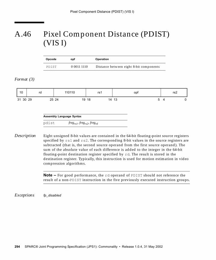
Pixel Component Distance (PDIST) (VIS I)
A.46 Pixel Component Distance (PDIST) (VIS I)
Format (3)
Description Eight unsigned 8-bit values are contained in the 64-bit floating-point source registers specified by rs1 and rs2. The corresponding 8-bit values in the source registers are subtracted (that is, the second source operand from the first source operand). The sum of the absolute value of each difference is added to the integer in the 64-bit floating-point destination register specified by rd. The result is stored in the destination register. Typically, this instruction is used for motion estimation in video compression algorithms.
Note – For good performance, the rd operand of PDIST should not reference the result of a non-PDIST instruction in the five previously executed instruction groups.
Exceptions fp_disabled
Opcode opf Operation
PDIST 0 0011 1110 Distance between eight 8-bit components
Assembly Language Syntax
pdist fregrs1, fregrs2, fregrd
31 24 02530 29 19 18 14 13 5 4
rd10 110110 opfrs1 rs2
294 SPARC® Joint Programming Specification (JPS1): Commonality • Release 1.0.4, 31 May 2002
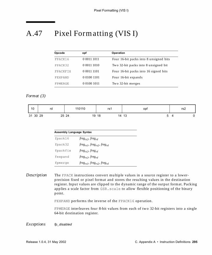
Pixel Formatting (VIS I)
A.47 Pixel Formatting (VIS I)
Format (3)
Description The FPACK instructions convert multiple values in a source register to a lower-precision fixed or pixel format and stores the resulting values in the destination register. Input values are clipped to the dynamic range of the output format. Packing applies a scale factor from GSR.scale to allow flexible positioning of the binary point.
FEXPAND performs the inverse of the FPACK16 operation.
FPMERGE interleaves four 8-bit values from each of two 32-bit registers into a single 64-bit destination register.
Exceptions fp_disabled
Opcode opf Operation
FPACK16 0 0011 1011 Four 16-bit packs into 8 unsigned bits
FPACK32 0 0011 1010 Two 32-bit packs into 8 unsigned bit
FPACKFIX 0 0011 1101 Four 16-bit packs into 16 signed bits
FEXPAND 0 0100 1101 Four 16-bit expands
FPMERGE 0 0100 1011 Two 32-bit merges
Assembly Language Syntax
fpack16 fregrs2, fregrd
fpack32 fregrs1, fregrs2, fregrd
fpackfix fregrs2, fregrd
fexpand fregrs2, fregrd
fpmerge fregrs1, fregrs2, fregrd
31 24 02530 29 19 18 14 13 5 4
rd10 110110 opfrs1 rs2
Release 1.0.4, 31 May 2002 C. Appendix A • Instruction Definitions 295
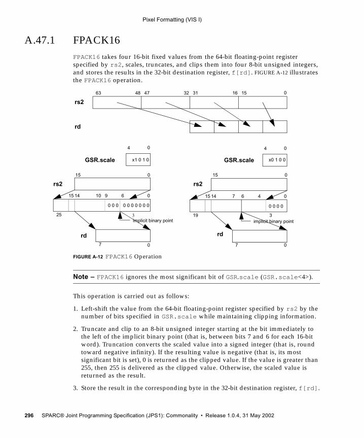
Pixel Formatting (VIS I)
A.47.1 FPACK16FPACK16 takes four 16-bit fixed values from the 64-bit floating-point register specified by rs2, scales, truncates, and clips them into four 8-bit unsigned integers, and stores the results in the 32-bit destination register, f[rd]. FIGURE A-12 illustrates the FPACK16 operation.
FIGURE A-12 FPACK16 Operation
Note – FPACK16 ignores the most significant bit of GSR.scale (GSR.scale<4>).
This operation is carried out as follows:
1. Left-shift the value from the 64-bit floating-point register specified by rs2 by the number of bits specified in GSR.scale while maintaining clipping information.
2. Truncate and clip to an 8-bit unsigned integer starting at the bit immediately to the left of the implicit binary point (that is, between bits 7 and 6 for each 16-bit word). Truncation converts the scaled value into a signed integer (that is, round toward negative infinity). If the resulting value is negative (that is, its most significant bit is set), 0 is returned as the clipped value. If the value is greater than 255, then 255 is delivered as the clipped value. Otherwise, the scaled value is returned as the result.
3. Store the result in the corresponding byte in the 32-bit destination register, f[rd].
015163132474863
04
x0 1 0 0GSR.scale
rs2
rd
067
19
0 0 0 0
1415 4
3implicit binary point
07
04
GSR.scale
0910
25
1415 6
3implicit binary point
07
0 0 0 0 0 0 0
x1 0 1 0
0 0 0
rs2 rs2
rd rd
015015
296 SPARC® Joint Programming Specification (JPS1): Commonality • Release 1.0.4, 31 May 2002
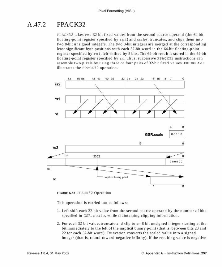
Pixel Formatting (VIS I)
A.47.2 FPACK32FPACK32 takes two 32-bit fixed values from the second source operand (the 64-bit floating-point register specified by rs2) and scales, truncates, and clips them into two 8-bit unsigned integers. The two 8-bit integers are merged at the corresponding least significant byte positions with each 32-bit word in the 64-bit floating-point register specified by rs1, left-shifted by 8 bits. The 64-bit result is stored in the 64-bit floating-point register specified by rd. Thus, successive FPACK32 instructions can assemble two pixels by using three or four pairs of 32-bit fixed values. FIGURE A-13 illustrates the FPACK32 operation.
FIGURE A-13 FPACK32 Operation
This operation is carried out as follows:
1. Left-shift each 32-bit value from the second source operand by the number of bits specified in GSR.scale, while maintaining clipping information.
2. For each 32-bit value, truncate and clip to an 8-bit unsigned integer starting at the bit immediately to the left of the implicit binary point (that is, between bits 23 and 22 for each 32-bit word). Truncation converts the scaled value into a signed integer (that is, round toward negative infinity). If the resulting value is negative
015163132474863
rs2
rd
04
GSR.scale
0
37
2223 5
implicit binary point
07
0 0 0 0 0 0
0 0 1 1 0
rs2
rd
015
56 55 40 39 24 23 8 7
rs1
31
Release 1.0.4, 31 May 2002 C. Appendix A • Instruction Definitions 297
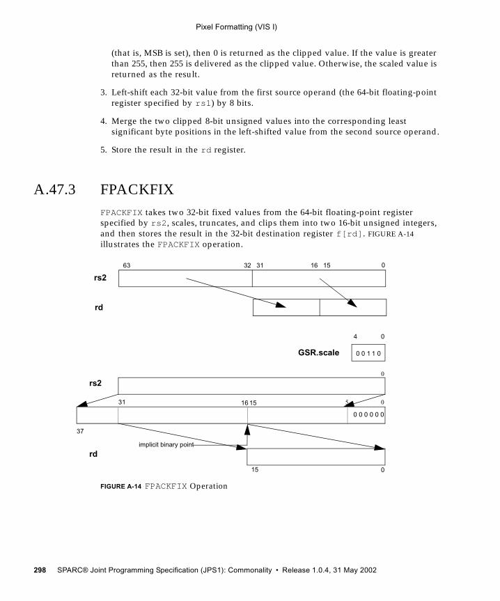
Pixel Formatting (VIS I)
(that is, MSB is set), then 0 is returned as the clipped value. If the value is greater than 255, then 255 is delivered as the clipped value. Otherwise, the scaled value is returned as the result.
3. Left-shift each 32-bit value from the first source operand (the 64-bit floating-point register specified by rs1) by 8 bits.
4. Merge the two clipped 8-bit unsigned values into the corresponding least significant byte positions in the left-shifted value from the second source operand.
5. Store the result in the rd register.
A.47.3 FPACKFIXFPACKFIX takes two 32-bit fixed values from the 64-bit floating-point register specified by rs2, scales, truncates, and clips them into two 16-bit unsigned integers, and then stores the result in the 32-bit destination register f[rd]. FIGURE A-14 illustrates the FPACKFIX operation.
FIGURE A-14 FPACKFIX Operation
01516313263
rs2
rd
04
GSR.scale
0
37
1516 5
implicit binary point
015
0 0 0 0 0 0
0 0 1 1 0
rs2
rd
0
31
298 SPARC® Joint Programming Specification (JPS1): Commonality • Release 1.0.4, 31 May 2002
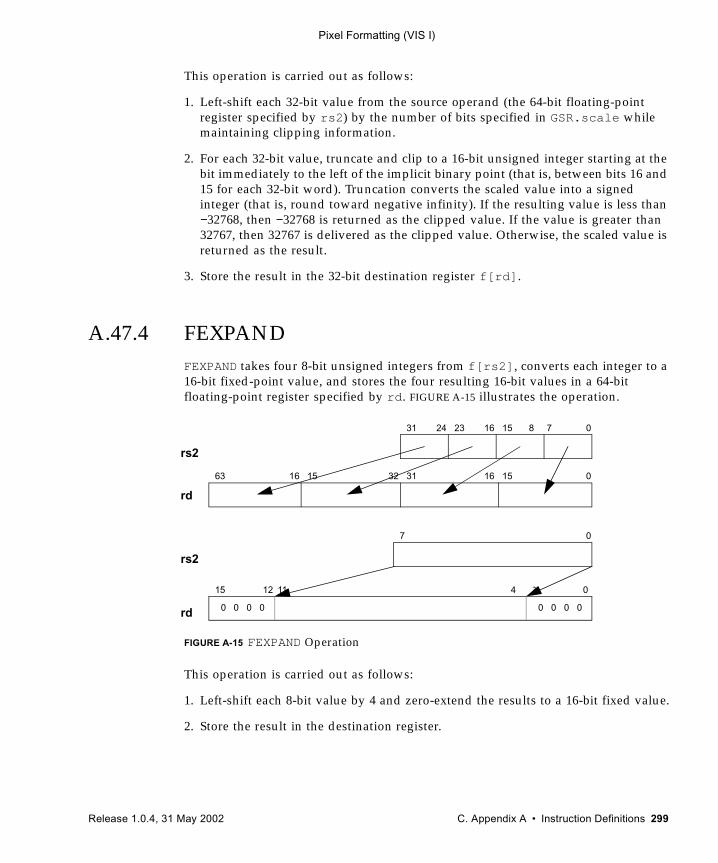
Pixel Formatting (VIS I)
This operation is carried out as follows:
1. Left-shift each 32-bit value from the source operand (the 64-bit floating-point register specified by rs2) by the number of bits specified in GSR.scale while maintaining clipping information.
2. For each 32-bit value, truncate and clip to a 16-bit unsigned integer starting at the bit immediately to the left of the implicit binary point (that is, between bits 16 and 15 for each 32-bit word). Truncation converts the scaled value into a signed integer (that is, round toward negative infinity). If the resulting value is less than −32768, then −32768 is returned as the clipped value. If the value is greater than 32767, then 32767 is delivered as the clipped value. Otherwise, the scaled value is returned as the result.
3. Store the result in the 32-bit destination register f[rd].
A.47.4 FEXPANDFEXPAND takes four 8-bit unsigned integers from f[rs2], converts each integer to a 16-bit fixed-point value, and stores the four resulting 16-bit values in a 64-bit floating-point register specified by rd. FIGURE A-15 illustrates the operation.
FIGURE A-15 FEXPAND Operation
This operation is carried out as follows:
1. Left-shift each 8-bit value by 4 and zero-extend the results to a 16-bit fixed value.
2. Store the result in the destination register.
01516313263
rs2
rd
1215 3
07
0 0 0 0
rs2
rd
011
1516
0151631 2324 78
0 0 0 0
4
Release 1.0.4, 31 May 2002 C. Appendix A • Instruction Definitions 299
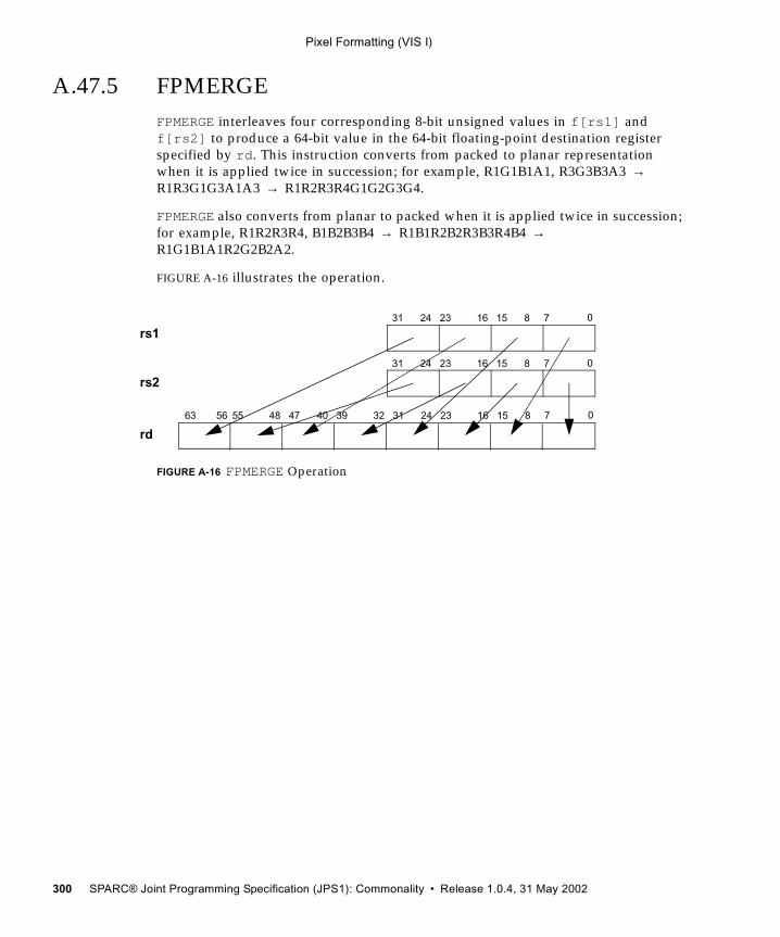
Pixel Formatting (VIS I)
A.47.5 FPMERGEFPMERGE interleaves four corresponding 8-bit unsigned values in f[rs1] and f[rs2] to produce a 64-bit value in the 64-bit floating-point destination register specified by rd. This instruction converts from packed to planar representation when it is applied twice in succession; for example, R1G1B1A1, R3G3B3A3 → R1R3G1G3A1A3 → R1R2R3R4G1G2G3G4.
FPMERGE also converts from planar to packed when it is applied twice in succession; for example, R1R2R3R4, B1B2B3B4 → R1B1R2B2R3B3R4B4 → R1G1B1A1R2G2B2A2.
FIGURE A-16 illustrates the operation.
FIGURE A-16 FPMERGE Operation
rd
015163132474863 56 55 40 39 24 23 8 7
0151631 24 23 8 7
0151631 24 23 8 7
rs1
rs2
300 SPARC® Joint Programming Specification (JPS1): Commonality • Release 1.0.4, 31 May 2002
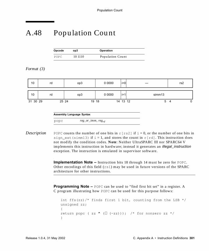
Population Count
A.48 Population Count
Format (3)
Description POPC counts the number of one bits in r[rs2] if i = 0, or the number of one bits in sign_ext(simm13) if i = 1, and stores the count in r[rd]. This instruction does not modify the condition codes. Note: Neither UltraSPARC III nor SPARC64 V implements this instruction in hardware; instead it generates an illegal_instruction exception. The instruction is emulated in supervisor software.
Implementation Note – Instruction bits 18 through 14 must be zero for POPC. Other encodings of this field (rs1) may be used in future versions of the SPARC architecture for other instructions.
Programming Note – POPC can be used to “find first bit set” in a register. A C program illustrating how POPC can be used for this purpose follows:
int ffs(zz)/* finds first 1 bit, counting from the LSB */unsigned zz;{return popc ( zz ^ (∼ (–zz))); /* for nonzero zz */}
Opcode op3 Operation
POPC 10 1110 Population Count
Assembly Language Syntax
popc reg_or_imm, regrd
31 24 02530 29 19 18
rd10 op3 —
14 13 12 5 4
0 0000 rs2i=0
rd10 op3 0 0000 simm13i=1
Release 1.0.4, 31 May 2002 C. Appendix A • Instruction Definitions 301
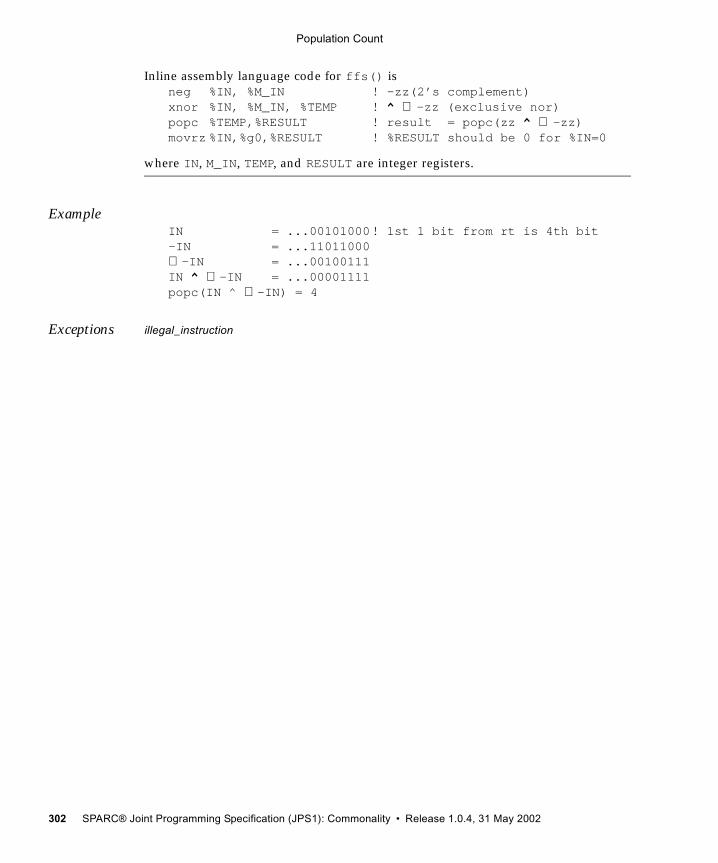
Population Count
Inline assembly language code for ffs() isneg %IN, %M_IN ! –zz(2’s complement)xnor %IN, %M_IN, %TEMP ! ^ ∼ –zz (exclusive nor)popc %TEMP,%RESULT ! result = popc(zz ^ ∼ –zz)movrz %IN,%g0,%RESULT ! %RESULT should be 0 for %IN=0
where IN, M_IN, TEMP, and RESULT are integer registers.
ExampleIN = ...00101000! 1st 1 bit from rt is 4th bit–IN = ...11011000∼ –IN = ...00100111IN ^ ∼ –IN = ...00001111popc(IN ^ ∼ –IN) = 4
Exceptions illegal_instruction
302 SPARC® Joint Programming Specification (JPS1): Commonality • Release 1.0.4, 31 May 2002
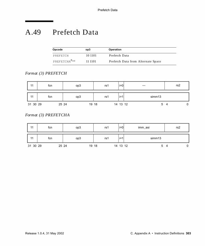
Prefetch Data
A.49 Prefetch Data
Format (3) PREFETCH
Format (3) PREFETCHA
Opcode op3 Operation
PREFETCH 10 1101 Prefetch Data
PREFETCHAPASI 11 1101 Prefetch Data from Alternate Space
31 24 02530 29 19 18 14 13 12 5 4
fcn11 op3 rs1 simm13i=1
fcn11 op3 rs1 i=0 — rs2
31 24 02530 29 19 18
fcn11 op3 imm_asi
14 13 12 5 4
rs1 rs2i=0
fcn11 op3 rs1 simm13i=1
Release 1.0.4, 31 May 2002 C. Appendix A • Instruction Definitions 303
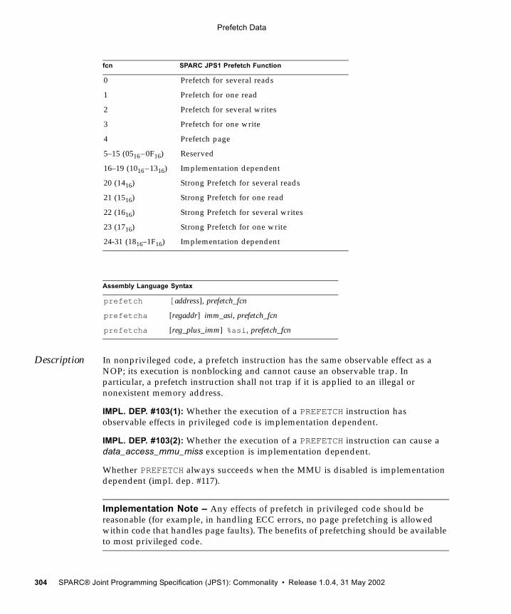
Prefetch Data
Description In nonprivileged code, a prefetch instruction has the same observable effect as a NOP; its execution is nonblocking and cannot cause an observable trap. In particular, a prefetch instruction shall not trap if it is applied to an illegal or nonexistent memory address.
IMPL. DEP. #103(1): Whether the execution of a PREFETCH instruction has observable effects in privileged code is implementation dependent.
IMPL. DEP. #103(2): Whether the execution of a PREFETCH instruction can cause a data_access_mmu_miss exception is implementation dependent.
Whether PREFETCH always succeeds when the MMU is disabled is implementation dependent (impl. dep. #117).
Implementation Note – Any effects of prefetch in privileged code should be reasonable (for example, in handling ECC errors, no page prefetching is allowed within code that handles page faults). The benefits of prefetching should be available to most privileged code.
fcn SPARC JPS1 Prefetch Function
0 Prefetch for several reads
1 Prefetch for one read
2 Prefetch for several writes
3 Prefetch for one write
4 Prefetch page
5–15 (0516–0F16) Reserved
16–19 (1016–1316) Implementation dependent
20 (1416) Strong Prefetch for several reads
21 (1516) Strong Prefetch for one read
22 (1616) Strong Prefetch for several writes
23 (1716) Strong Prefetch for one write
24-31 (1816–1F16) Implementation dependent
Assembly Language Syntax
prefetch [address], prefetch_fcn
prefetcha [regaddr] imm_asi, prefetch_fcn
prefetcha [reg_plus_imm] %asi, prefetch_fcn
304 SPARC® Joint Programming Specification (JPS1): Commonality • Release 1.0.4, 31 May 2002
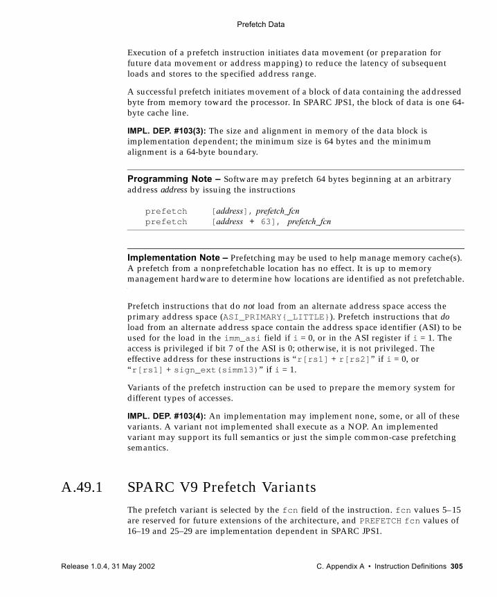
Prefetch Data
Execution of a prefetch instruction initiates data movement (or preparation for future data movement or address mapping) to reduce the latency of subsequent loads and stores to the specified address range.
A successful prefetch initiates movement of a block of data containing the addressed byte from memory toward the processor. In SPARC JPS1, the block of data is one 64-byte cache line.
IMPL. DEP. #103(3): The size and alignment in memory of the data block is implementation dependent; the minimum size is 64 bytes and the minimum alignment is a 64-byte boundary.
Programming Note – Software may prefetch 64 bytes beginning at an arbitrary address address by issuing the instructions
prefetch [address], prefetch_fcnprefetch [address + 63], prefetch_fcn
Implementation Note – Prefetching may be used to help manage memory cache(s). A prefetch from a nonprefetchable location has no effect. It is up to memory management hardware to determine how locations are identified as not prefetchable.
Prefetch instructions that do not load from an alternate address space access the primary address space (ASI_PRIMARY{_LITTLE}). Prefetch instructions that do load from an alternate address space contain the address space identifier (ASI) to be used for the load in the imm_asi field if i = 0, or in the ASI register if i = 1. The access is privileged if bit 7 of the ASI is 0; otherwise, it is not privileged. The effective address for these instructions is “r[rs1] + r[rs2]” if i = 0, or “r[rs1] + sign_ext(simm13)” if i = 1.
Variants of the prefetch instruction can be used to prepare the memory system for different types of accesses.
IMPL. DEP. #103(4): An implementation may implement none, some, or all of these variants. A variant not implemented shall execute as a NOP. An implemented variant may support its full semantics or just the simple common-case prefetching semantics.
A.49.1 SPARC V9 Prefetch VariantsThe prefetch variant is selected by the fcn field of the instruction. fcn values 5–15 are reserved for future extensions of the architecture, and PREFETCH fcn values of 16–19 and 25–29 are implementation dependent in SPARC JPS1.
Release 1.0.4, 31 May 2002 C. Appendix A • Instruction Definitions 305
Prefetch Data
Each prefetch variant reflects an intent on the part of the compiler or programmer. This is different from other instructions in SPARC V9 (except BPN), all of which specify specific actions. An implementation may implement a prefetch variant by any technique, as long as the intent of the variant is achieved.
The prefetch instruction is designed to treat the common cases as well. The variants are intended to provide scalability for future improvements in both hardware and compilers. If a variant is implemented, it should have the effects described below. In case some of the variants listed below are implemented and some are not, a recommended overloading of the unimplemented variants is provided in the SPARC V9 specification.
Prefetch for Several Reads (fcn = 0)
The intent of this variant is to cause movement of data into the data cache nearest the processor, with “reasonable” efforts made to obtain the data.
Programming Note – The intended use of this variant is in streaming relatively small amounts of data into the primary data cache of the processor.
Prefetch for One Read (fcn = 1)
The data to be read from the given address is expected to be read once and not reused (read or written) soon after that. Use of this PREFETCH variant indicates that, if possible, the data cache should be minimally disturbed by the data read from the given address.
Programming Note – The intended use of this variant is in streaming medium amounts of data into the processor without disturbing the data in the primary data cache memory.
Prefetch for Several Writes (and Possibly Reads) (fcn = 2)
The intent of this variant is to cause movement of data in preparation for writing.
Programming Note – An example use of this variant is to initialize a cache line in preparation for a partial write.
306 SPARC® Joint Programming Specification (JPS1): Commonality • Release 1.0.4, 31 May 2002
Prefetch Data
Implementation Note – On a multiprocessor, this variant indicates that exclusive ownership of the addressed data is needed, so it may have the additional effect of obtaining exclusive ownership of the addressed cache line.
Prefetch for One Write (fcn = 3)
This variant indicates that, if possible, the data cache should be minimally disturbed by the data written to this address, because those data are not expected to be reused (read or written) soon after they have been written once.
Prefetch Page (fcn = 4)
In a virtual memory system, the intended action of this variant is for the supervisor software or hardware to initiate asynchronous mapping of the referenced virtual address, assuming that it is legal to do so.
Programming Note – The desire is to avoid a later page fault for the given address, or at least to shorten the latency of a page fault.
In a non-virtual-memory system or if the addressed page is already mapped, this variant has no effect.
The referenced page need not be mapped when the instruction completes. Loads and stores issued before the page is mapped should block just as they would if the prefetch had never been issued. When the activity associated with the mapping has completed, the loads and stores may proceed.
Implementation Notes– An example of mapping activity is DMA from secondary storage.
Use of this variant may be disabled or restricted in privileged code that is not permitted to cause page faults.
SPARC JPS1 treats this variant as a NOP; no operation is performed.
A.49.2 SPARC JPS1 Prefetch Variants (fcn = 20–23)
These values are available for implementations to use. An implementation shall treat any unimplemented prefetch fcn values as NOPs (impl. dep. #103).
Release 1.0.4, 31 May 2002 C. Appendix A • Instruction Definitions 307
Prefetch Data
Strong Prefetch for Several Reads (fcn =20)
The intent of this variant is the same as for Prefetch for Several Reads (fcn = 0) except this variant may cause an exception if access causes a TLB miss.
Strong Prefetch for One Read (fcn = 21)
The intent of this variant is the same as for Prefetch for One Read (fcn = 1) except this variant may cause an exception if this access causes a TLB miss.
Strong Prefetch for Several Writes (fcn = 22)
The intent of this variant is the same as for Prefetch for Several Writes (fcn = 2) except this variant may cause an exception if this access causes TLB miss.
Strong Prefetch for One Write (fcn = 23)
The intent of this variant is the same as for Prefetch for One Write (fcn = 3) except this variant may cause an exception if this access causes a TLB miss.
A.49.3 Implementation-Dependent Prefetch Variants (fcn = 16–19, 24–31)fcns 16-19 and 24-31 are implementation dependent.
308 SPARC® Joint Programming Specification (JPS1): Commonality • Release 1.0.4, 31 May 2002
Prefetch Data
Implementation Note – It is desirable to avoid conflicting uses of the same prefetch function code on different implementation; the following is a list of function codes that are either implemented in JPS1 implementations or are expected to be used in future implementations, and their respective uses:
fcn Expected Use
16 Prefetch Invalidate17 NOP18 NOP19 NOP20 Strong Prefetch for read21 Strong Prefetch for read22 Strong Prefetch for write23 Strong Prefetch for write24 Invalidate Cache Entry25 NOP26 NOP27 NOP28 NOP29 NOP 30 NOP31 NOP
Please refer to Implementation Supplements for details.
A.49.4 General CommentsThere is no variant of PREFETCH for instruction prefetching. Instruction prefetching should be encoded with the Branch Never (BPN) form of the BPcc instruction (see A.8, Branch on Integer Condition Codes with Prediction (BPcc), on page 210).
One error to avoid in thinking about prefetch instructions is that they should have “no cost to execute.” As long as the cost of executing a prefetch instruction is well less than one-third the cost of a cache miss, use of prefetching is a net win. It does not appear that prefetching causes a significant number of useless fetches from memory, though it may increase the rate of useful fetches (and hence the bandwidth), because it more efficiently overlaps computing with fetching.
Release 1.0.4, 31 May 2002 C. Appendix A • Instruction Definitions 309
Prefetch Data
Programming Note – A SPARC V9 compiler that generates PREFETCH instructions should generate each of the variants where it is most appropriate. The overloadings suggested in the previous Implementation Note ensure that such code will be portable and reasonably efficient across a range of hardware configurations.
Implementation Note – The Prefetch for One Read and Prefetch for One Write variants assume the existence of a “bypass cache,” so that the bulk of the “real cache” remains undisturbed. If such a bypass cache is used, it should be large enough to properly shield the processor from memory latency. Such a cache should probably be small, highly associative, and use a FIFO replacement policy.
Exceptions illegal_instruction (fcn = 5–15)fast_data_access_MMU_miss (fcn = 20–23)
310 SPARC® Joint Programming Specification (JPS1): Commonality • Release 1.0.4, 31 May 2002
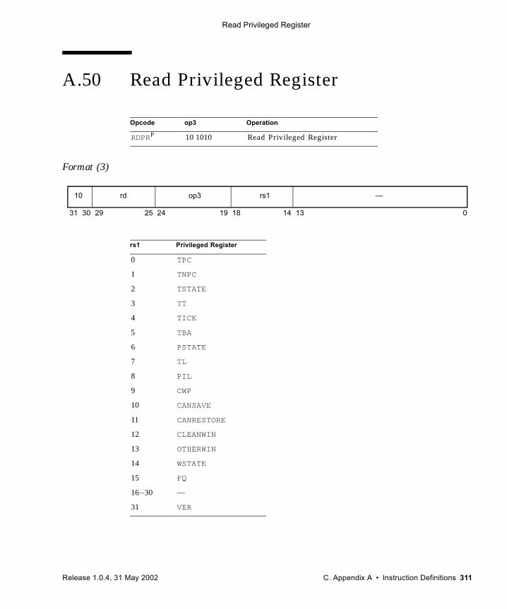
Read Privileged Register
A.50 Read Privileged Register
Format (3)
Opcode op3 Operation
RDPRP 10 1010 Read Privileged Register
rs1 Privileged Register
0 TPC
1 TNPC
2 TSTATE
3 TT
4 TICK
5 TBA
6 PSTATE
7 TL
8 PIL
9 CWP
10 CANSAVE
11 CANRESTORE
12 CLEANWIN
13 OTHERWIN
14 WSTATE
15 FQ
16–30 —
31 VER
31 141924 18 13 02530 29
10 rd op3 rs1 —
Release 1.0.4, 31 May 2002 C. Appendix A • Instruction Definitions 311
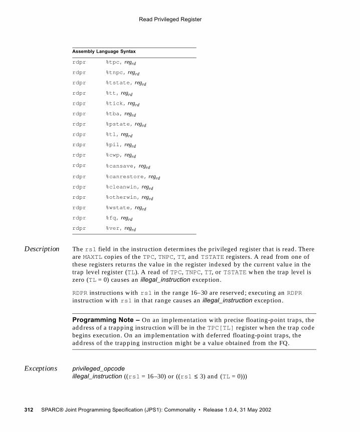
Read Privileged Register
Description The rs1 field in the instruction determines the privileged register that is read. There are MAXTL copies of the TPC, TNPC, TT, and TSTATE registers. A read from one of these registers returns the value in the register indexed by the current value in the trap level register (TL). A read of TPC, TNPC, TT, or TSTATE when the trap level is zero (TL = 0) causes an illegal_instruction exception.
RDPR instructions with rs1 in the range 16–30 are reserved; executing an RDPR instruction with rs1 in that range causes an illegal_instruction exception.
Programming Note – On an implementation with precise floating-point traps, the address of a trapping instruction will be in the TPC[TL] register when the trap code begins execution. On an implementation with deferred floating-point traps, the address of the trapping instruction might be a value obtained from the FQ.
Exceptions privileged_opcodeillegal_instruction ((rs1 = 16–30) or ((rs1 ≤ 3) and (TL = 0)))
Assembly Language Syntax
rdpr %tpc, regrd
rdpr %tnpc, regrd
rdpr %tstate, regrd
rdpr %tt, regrd
rdpr %tick, regrd
rdpr %tba, regrd
rdpr %pstate, regrd
rdpr %tl, regrd
rdpr %pil, regrd
rdpr %cwp, regrd
rdpr %cansave, regrd
rdpr %canrestore, regrd
rdpr %cleanwin, regrd
rdpr %otherwin, regrd
rdpr %wstate, regrd
rdpr %fq, regrd
rdpr %ver, regrd
312 SPARC® Joint Programming Specification (JPS1): Commonality • Release 1.0.4, 31 May 2002
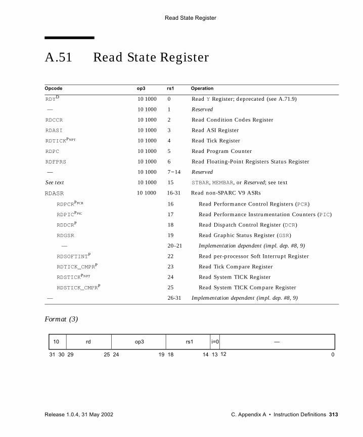
Read State Register
A.51 Read State Register
Format (3)
Opcode op3 rs1 Operation
RDYD 10 1000 0 Read Y Register; deprecated (see A.71.9)
— 10 1000 1 Reserved
RDCCR 10 1000 2 Read Condition Codes Register
RDASI 10 1000 3 Read ASI Register
RDTICKPNPT 10 1000 4 Read Tick Register
RDPC 10 1000 5 Read Program Counter
RDFPRS 10 1000 6 Read Floating-Point Registers Status Register
— 10 1000 7−14 Reserved
See text 10 1000 15 STBAR, MEMBAR, or Reserved; see text
RDASR 10 1000 16-31 Read non-SPARC V9 ASRs
RDPCRPPCR 16 Read Performance Control Registers (PCR)
RDPICPPIC 17 Read Performance Instrumentation Counters (PIC)
RDDCRP 18 Read Dispatch Control Register (DCR)
RDGSR 19 Read Graphic Status Register (GSR)
— 20–21 Implementation dependent (impl. dep. #8, 9)
RDSOFTINTP 22 Read per-processor Soft Interrupt Register
RDTICK_CMPRP 23 Read Tick Compare Register
RDSTICKPNPT 24 Read System TICK Register
RDSTICK_CMPRP 25 Read System TICK Compare Register
— 26-31 Implementation dependent (impl. dep. #8, 9)
31 141924 18 13 02530 29
10 rd op3 rs1 —
12
i=0
Release 1.0.4, 31 May 2002 C. Appendix A • Instruction Definitions 313
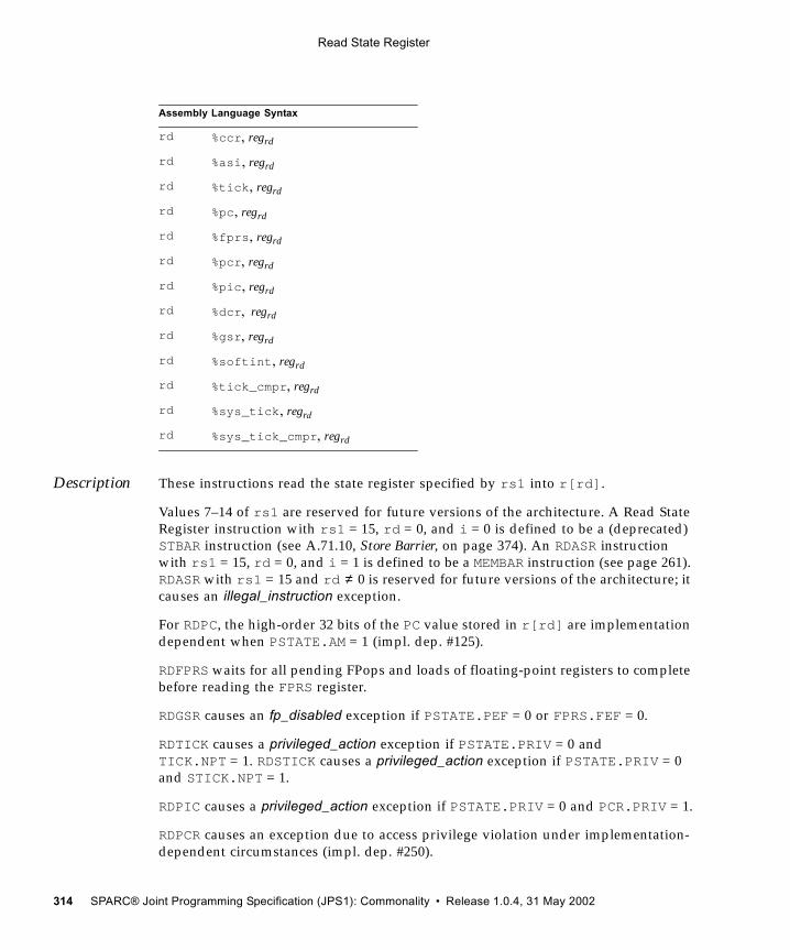
Read State Register
Description These instructions read the state register specified by rs1 into r[rd].
Values 7–14 of rs1 are reserved for future versions of the architecture. A Read State Register instruction with rs1 = 15, rd = 0, and i = 0 is defined to be a (deprecated) STBAR instruction (see A.71.10, Store Barrier, on page 374). An RDASR instruction with rs1 = 15, rd = 0, and i = 1 is defined to be a MEMBAR instruction (see page 261). RDASR with rs1 = 15 and rd ≠ 0 is reserved for future versions of the architecture; it causes an illegal_instruction exception.
For RDPC, the high-order 32 bits of the PC value stored in r[rd] are implementation dependent when PSTATE.AM = 1 (impl. dep. #125).
RDFPRS waits for all pending FPops and loads of floating-point registers to complete before reading the FPRS register.
RDGSR causes an fp_disabled exception if PSTATE.PEF = 0 or FPRS.FEF = 0.
RDTICK causes a privileged_action exception if PSTATE.PRIV = 0 and TICK.NPT = 1. RDSTICK causes a privileged_action exception if PSTATE.PRIV = 0 and STICK.NPT = 1.
RDPIC causes a privileged_action exception if PSTATE.PRIV = 0 and PCR.PRIV = 1.
RDPCR causes an exception due to access privilege violation under implementation-dependent circumstances (impl. dep. #250).
Assembly Language Syntax
rd %ccr, regrd
rd %asi, regrd
rd %tick, regrd
rd %pc, regrd
rd %fprs, regrd
rd %pcr, regrd
rd %pic, regrd
rd %dcr, regrd
rd %gsr, regrd
rd %softint, regrd
rd %tick_cmpr, regrd
rd %sys_tick, regrd
rd %sys_tick_cmpr, regrd
314 SPARC® Joint Programming Specification (JPS1): Commonality • Release 1.0.4, 31 May 2002
Read State Register
Note – See Section I.1, Read/Write Ancillary State Registers (ASRs), for a discussion of extending the SPARC V9 instruction set using read/write ASR instructions.
Implementation Note – Ancillary state registers may include (for example) timer, counter, diagnostic, self-test, and trap-control registers. See Implementation Characteristics of Current SPARC-V9-based Products, Revision 9.x, a document available from SPARC International, for information on implemented ancillary state registers.
Compatibility Note – The SPARC V8 RDPSR, RDWIM, and RDTBR instructions do not exist in SPARC V9 since the PSR, WIM, and TBR registers do not exist in SPARC V9.
Exceptions privileged_opcode(RDDCR, RDSOFTINT, RDTICK_CMPR, RDSTICK, RDSTICK_CMPR, and RDPCR (impl. dep. #250))illegal_instruction(RDASR with rs1 = 1 or 7–14;
RDASR with rs1 = 15 and rd ≠ 0;RDASR with rs1 = 20–21, 26–31)
privileged_action (RDTICK with PSTATE.PRIV = 0 and TICK.NPT = 1;RDPIC with PSTATE.PRIV = 0 and PCR.PRIV = 1;RDSTICK with PSTATE.PRIV = 0 and STICK.NPT = 1;RDPCR (impl. dep. #250))
fp_disabled (RDGSR with PSTATE.PEF = 0 or FPRS.FEF = 0)
Release 1.0.4, 31 May 2002 C. Appendix A • Instruction Definitions 315
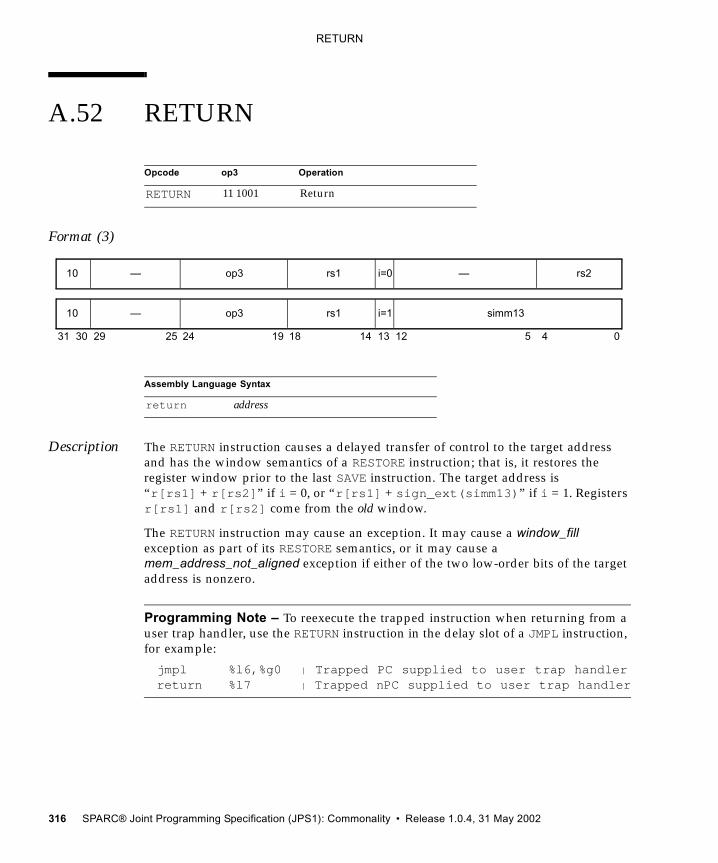
RETURN
A.52 RETURN
Format (3)
Description The RETURN instruction causes a delayed transfer of control to the target address and has the window semantics of a RESTORE instruction; that is, it restores the register window prior to the last SAVE instruction. The target address is “r[rs1] + r[rs2]” if i = 0, or “r[rs1] + sign_ext(simm13)” if i = 1. Registers r[rs1] and r[rs2] come from the old window.
The RETURN instruction may cause an exception. It may cause a window_fill exception as part of its RESTORE semantics, or it may cause a mem_address_not_aligned exception if either of the two low-order bits of the target address is nonzero.
Programming Note – To reexecute the trapped instruction when returning from a user trap handler, use the RETURN instruction in the delay slot of a JMPL instruction, for example:
jmpl %l6,%g0 | Trapped PC supplied to user trap handlerreturn %l7 | Trapped nPC supplied to user trap handler
Opcode op3 Operation
RETURN 11 1001 Return
Assembly Language Syntax
return address
31 24 02530 29 19 18
—10 op3 —
14 13 12 5 4
rs1 rs2i=0
10 op3 rs1 simm13i=1—
316 SPARC® Joint Programming Specification (JPS1): Commonality • Release 1.0.4, 31 May 2002
RETURN
Programming Note – A routine that uses a register window may be structured either as
save %sp,-framesize, %sp. . .ret | Same as jmpl %i7 + 8, %g0restore | Something useful like “restore
| %o2,%l2,%o0”
or as
save %sp,-framesize, %sp. . .return %i7 + 8nop | Could do some useful work in the caller’s
| window, e.g., “or %o1, %o2,%o0”
Exceptions mem_address_not_alignedfill_n_normal (n = 0–7)fill_n_other (n = 0–7)
Release 1.0.4, 31 May 2002 C. Appendix A • Instruction Definitions 317
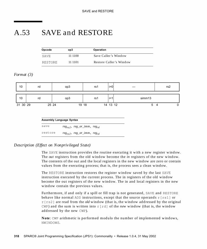
SAVE and RESTORE
A.53 SAVE and RESTORE
Format (3)
Description (Effect on Nonprivileged State)
The SAVE instruction provides the routine executing it with a new register window. The out registers from the old window become the in registers of the new window. The contents of the out and the local registers in the new window are zero or contain values from the executing process; that is, the process sees a clean window.
The RESTORE instruction restores the register window saved by the last SAVE instruction executed by the current process. The in registers of the old window become the out registers of the new window. The in and local registers in the new window contain the previous values.
Furthermore, if and only if a spill or fill trap is not generated, SAVE and RESTORE behave like normal ADD instructions, except that the source operands r[rs1] or r[rs2] are read from the old window (that is, the window addressed by the original CWP) and the sum is written into r[rd] of the new window (that is, the window addressed by the new CWP).
Note: CWP arithmetic is performed modulo the number of implemented windows, NWINDOWS.
Opcode op3 Operation
SAVE 11 1100 Save Caller’s Window
RESTORE 11 1101 Restore Caller’s Window
Assembly Language Syntax
save regrs1, reg_or_imm, regrd
restore regrs1, reg_or_imm, regrd
31 24 02530 29 19 18
rd10 op3 —
14 13 12 5 4
rs1 rs2i=0
10 op3 rs1 simm13i=1rd
318 SPARC® Joint Programming Specification (JPS1): Commonality • Release 1.0.4, 31 May 2002
SAVE and RESTORE
Programming Notes – Typically, if a SAVE (RESTORE) instruction traps, the spill (fill) trap handler returns to the trapped instruction to reexecute it. So, although the ADD operation is not performed the first time (when the instruction traps), it is performed the second time the instruction executes. The same applies to changing the CWP.
The SAVE instruction can be used to atomically allocate a new window in the register file and a new software stack frame in memory. See H.1.2, Leaf-Procedure Optimization, for details.
There is a performance trade-off to consider between using SAVE/RESTORE and saving and restoring selected registers explicitly.
Description (Effect on Privileged State)
If the SAVE instruction does not trap, it increments the CWP (mod NWINDOWS) to provide a new register window and updates the state of the register windows by decrementing CANSAVE and incrementing CANRESTORE.
If the new register window is occupied (that is, CANSAVE = 0), a spill trap is generated. The trap vector for the spill trap is based on the value of OTHERWIN and WSTATE. The spill trap handler is invoked with the CWP set to point to the window to be spilled (that is, old CWP + 2).
If CANSAVE ≠ 0, the SAVE instruction checks whether the new window needs to be cleaned. It causes a clean_window trap if the number of unused clean windows is zero, that is, (CLEANWIN – CANRESTORE) = 0. The clean_window trap handler is invoked with the CWP set to point to the window to be cleaned (that is, old CWP + 1).
If the RESTORE instruction does not trap, it decrements the CWP (mod NWINDOWS) to restore the register window that was in use prior to the last SAVE instruction executed by the current process. It also updates the state of the register windows by decrementing CANRESTORE and incrementing CANSAVE.
If the register window to be restored has been spilled (CANRESTORE = 0), then a fill trap is generated. The trap vector for the fill trap is based on the values of OTHERWIN and WSTATE, as described in Trap Type for Spill/Fill Traps on page 147. The fill trap handler is invoked with CWP set to point to the window to be filled, that is, old CWP – 1.
Release 1.0.4, 31 May 2002 C. Appendix A • Instruction Definitions 319
SAVE and RESTORE
Programming Note – The vectoring of spill and fill traps can be controlled by setting the value of the OTHERWIN and WSTATE registers appropriately. For details, see Splitting the Register Windows in H.2.3, Client-Server Model.
The spill (fill) handler normally will end with a SAVED (RESTORED) instruction followed by a RETRY instruction.
Exceptions clean_window (SAVE only)fill_n_normal (RESTORE only, n =0–7)fill_n_other (RESTORE only, n = 0–7)spill_n_normal (SAVE only, n = 0–7)spill_n_other (SAVE only, n = 0–7)
320 SPARC® Joint Programming Specification (JPS1): Commonality • Release 1.0.4, 31 May 2002
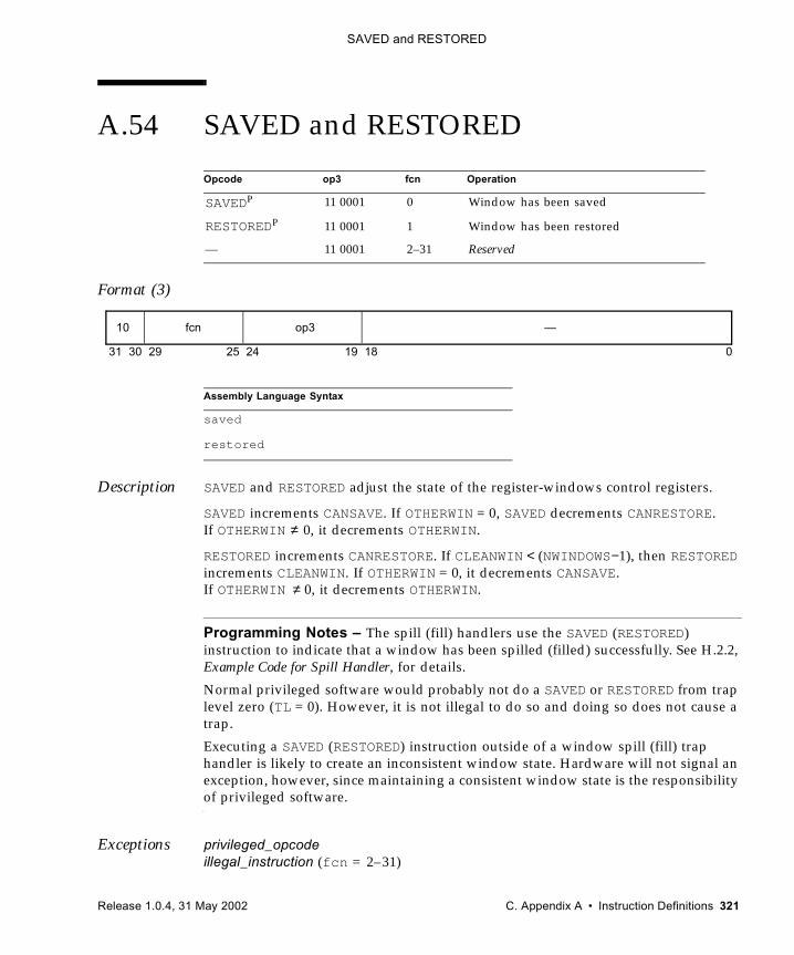
SAVED and RESTORED
A.54 SAVED and RESTORED
Format (3)
Description SAVED and RESTORED adjust the state of the register-windows control registers.
SAVED increments CANSAVE. If OTHERWIN = 0, SAVED decrements CANRESTORE. If OTHERWIN ≠ 0, it decrements OTHERWIN.
RESTORED increments CANRESTORE. If CLEANWIN < (NWINDOWS−1), then RESTORED increments CLEANWIN. If OTHERWIN = 0, it decrements CANSAVE. If OTHERWIN ≠ 0, it decrements OTHERWIN.
Programming Notes – The spill (fill) handlers use the SAVED (RESTORED) instruction to indicate that a window has been spilled (filled) successfully. See H.2.2, Example Code for Spill Handler, for details.
Normal privileged software would probably not do a SAVED or RESTORED from trap level zero (TL = 0). However, it is not illegal to do so and doing so does not cause a trap.
Executing a SAVED (RESTORED) instruction outside of a window spill (fill) trap handler is likely to create an inconsistent window state. Hardware will not signal an exception, however, since maintaining a consistent window state is the responsibility of privileged software.
Exceptions privileged_opcodeillegal_instruction (fcn = 2–31)
Opcode op3 fcn Operation
SAVEDP 11 0001 0 Window has been saved
RESTOREDP 11 0001 1 Window has been restored
— 11 0001 2–31 Reserved
Assembly Language Syntax
saved
restored
31 1924 18 02530 29
10 fcn op3 —
Release 1.0.4, 31 May 2002 C. Appendix A • Instruction Definitions 321
Set Interval Arithmetic Mode (VIS II)
A.55 Set Interval Arithmetic Mode (VIS II)
Format (3)
Description The SIAM instruction sets the GSR.IM and GSR.IRND fields as follows:
GSR.IM = mode<2>
GSR.IRND = mode<1:0>
Exceptions fp_disabled
Opcode opf Operation
SIAM 0 1000 0001 Set the interval arithmetic mode fields in the GSR
Assembly Language Syntax
siam mode
31 24 02530 29 19 18 14 13 5 4
—10 110110 opf— — mode
3 2
322 SPARC® Joint Programming Specification (JPS1): Commonality • Release 1.0.4, 31 May 2002
SETHI
A.56 SETHI
Format (2)
Description SETHI zeroes the least significant 10 bits and the most significant 32 bits of r[rd] and replaces bits 31 through 10 of r[rd] with the value from its imm22 field.
SETHI does not affect the condition codes.
Some SETHI instructions with rd = 0 have special uses:
■ rd = 0 and imm22 = 0: defined to be a NOP instruction (described in A.41)
■ rd = 0 and imm22 ≠ 0 may be used to trigger hardware performance counters in some JPS1 implementations (for details, see Appendix Q in each JPS1 Implementation Supplement).
Programming Note – The most common form of 64-bit constant generation is creating stack offsets whose magnitude is less than 232. The code below can be used to create the constant 0000 0000 ABCD 123416:
sethi %hi(0xabcd1234),%o0or %o0, 0x234, %o0
The following code shows how to create a negative constant. Note: The immediate field of the xor instruction is sign extended and can be used to get 1’s in all of the upper 32 bits. For example, to set the negative constant FFFF FFFF ABCD 123416:
sethi %hi(0x5432edcb),%o0 ! note 0x5432EDCB, not 0xABCD1234xor %o0, 0x1e34, %o0 ! part of imm. overlaps upper bits
Exceptions None
Opcode op2 Operation
SETHI 100 Set High 22 Bits of Low Word
Assembly Language Syntax
sethi const22, regrd
sethi %hi (value), regrd
31 2224 21 02530 29
00 rd op2 imm22
Release 1.0.4, 31 May 2002 C. Appendix A • Instruction Definitions 323
Shift
A.57 Shift
Format (3)
Description When i = 0 and x = 0, the shift count is the least significant five bits of r[rs2]. When i = 0 and x = 1, the shift count is the least significant six bits of r[rs2]. When i = 1 and x = 0, the shift count is the immediate value specified in bits 0 through 4 of the instruction. When i = 1 and x = 1, the shift count is the immediate value specified in bits 0 through 5 of the instruction.
Opcode op3 x Operation
SLL 10 0101 0 Shift Left Logical – 32 bits
SRL 10 0110 0 Shift Right Logical – 32 bits
SRA 10 0111 0 Shift Right Arithmetic– 32 bits
SLLX 10 0101 1 Shift Left Logical – 64 bits
SRLX 10 0110 1 Shift Right Logical – 64 bits
SRAX 10 0111 1 Shift Right Arithmetic – 64 bits
Assembly Language Syntax
sll regrs1, reg_or_shcnt, regrd
srl regrs1, reg_or_shcnt, regrd
sra regrs1, reg_or_shcnt, regrd
sllx regrs1, reg_or_shcnt, regrd
srlx regrs1, reg_or_shcnt, regrd
srax regrs1, reg_or_shcnt, regrd
31 24 02530 29 19 18
rd10 op3 —
14 13 12 5 4
rs1 rs2i=0 x
rd10 op3 —rs1 shcnt32i=1 x=0
rd10 op3 —rs1 shcnt64i=1 x=1
6
324 SPARC® Joint Programming Specification (JPS1): Commonality • Release 1.0.4, 31 May 2002
Shift
TABLE A-8 shows the shift count encodings for all values of i and x.
SLL and SLLX shift all 64 bits of the value in r[rs1] left by the number of bits specified by the shift count, replacing the vacated positions with zeroes, and write the shifted result to r[rd].
SRL shifts the low 32 bits of the value in r[rs1] right by the number of bits specified by the shift count. Zeroes are shifted into bit 31. The upper 32 bits are set to zero, and the result is written to r[rd].
SRLX shifts all 64 bits of the value in r[rs1] right by the number of bits specified by the shift count. Zeroes are shifted into the vacated high-order bit positions, and the shifted result is written to r[rd].
SRA shifts the low 32 bits of the value in r[rs1] right by the number of bits specified by the shift count and replaces the vacated positions with bit 31 of r[rs1]. The high-order 32 bits of the result are all set with bit 31 of r[rs1], and the result is written to r[rd].
SRAX shifts all 64 bits of the value in r[rs1] right by the number of bits specified by the shift count and replaces the vacated positions with bit 63 of r[rs1]. The shifted result is written to r[rd].
No shift occurs when the shift count is 0, but the high-order bits are affected by the 32-bit shifts as noted above.
These instructions do not modify the condition codes.
Programming Notes – “Arithmetic left shift by 1 (and calculate overflow)” can be effected with the ADDcc instruction.
The instruction “sra rs1,0,rd” can be used to convert a 32-bit value to 64 bits, with sign extension into the upper word. “srl rs1,0,rd” can be used to clear the upper 32 bits of r[rd].
Exceptions None
TABLE A-8 Shift Count Encodings
i x Shift Count
0 0 bits 4–0 of r[rs2]
0 1 bits 5–0 of r[rs2]
1 0 bits 4–0 of instruction
1 1 bits 5–0 of instruction
Release 1.0.4, 31 May 2002 C. Appendix A • Instruction Definitions 325
Short Floating-Point Load and Store (VIS I)
A.58 Short Floating-Point Load and Store (VIS I)
Format (3) LDDFA
Format (3) STDFA
Opcode imm_asi ASI Value Operation
LDDFASTDFA
ASI_FL8_P D016 8-bit load/store from/to primary address space
LDDFASTDFA
ASI_FL8_S D116 8-bit load/store from/to secondary address space
LDDFASTDFA
ASI_FL8_PL D816 8-bit load/store from/to primary address space, little-endian
LDDFASTDFA
ASI_FL8_SL D916 8-bit load/store from/to secondary address space, little-endian
LDDFASTDFA
ASI_FL16_P D216 16-bit load/store from/to primary address space
LDDFASTDFA
ASI_FL16_S D316 16-bit load/store from/to secondary address space
LDDFASTDFA
ASI_FL16_PL DA16 16-bit load/store from/to primary address space, little-endian
LDDFASTDFA
ASI_FL16_SL DB16 16-bit load/store from/to secondary address space, little-endian
31 24 02530 29 19 18 14 13 5 4
rd11 110011 simm_13rs1 i=1
rd11 110011 imm_asirs1 rs2i=0
31 24 02530 29 19 18 14 13 5 4
rd11 110111 simm_13rs1 i=1
rd11 110111 imm_asirs1 rs2i=0
326 SPARC® Joint Programming Specification (JPS1): Commonality • Release 1.0.4, 31 May 2002
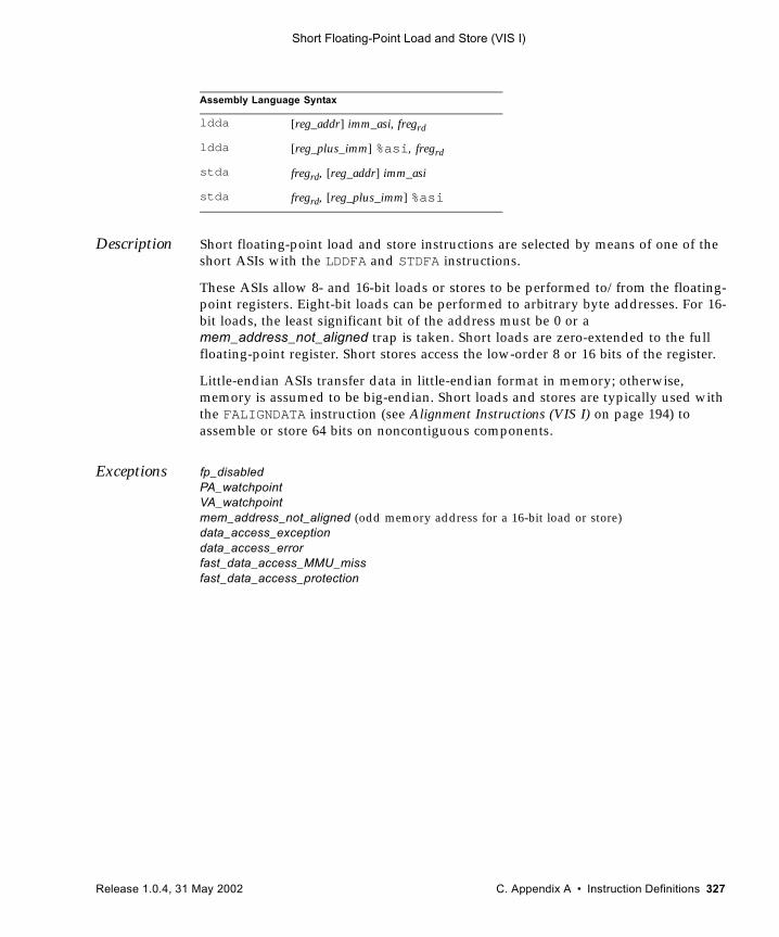
Short Floating-Point Load and Store (VIS I)
Description Short floating-point load and store instructions are selected by means of one of the short ASIs with the LDDFA and STDFA instructions.
These ASIs allow 8- and 16-bit loads or stores to be performed to/from the floating-point registers. Eight-bit loads can be performed to arbitrary byte addresses. For 16-bit loads, the least significant bit of the address must be 0 or a mem_address_not_aligned trap is taken. Short loads are zero-extended to the full floating-point register. Short stores access the low-order 8 or 16 bits of the register.
Little-endian ASIs transfer data in little-endian format in memory; otherwise, memory is assumed to be big-endian. Short loads and stores are typically used with the FALIGNDATA instruction (see Alignment Instructions (VIS I) on page 194) to assemble or store 64 bits on noncontiguous components.
Exceptions fp_disabledPA_watchpointVA_watchpointmem_address_not_aligned (odd memory address for a 16-bit load or store)data_access_exceptiondata_access_errorfast_data_access_MMU_missfast_data_access_protection
Assembly Language Syntax
ldda [reg_addr] imm_asi, fregrd
ldda [reg_plus_imm] %asi, fregrd
stda fregrd, [reg_addr] imm_asi
stda fregrd, [reg_plus_imm] %asi
Release 1.0.4, 31 May 2002 C. Appendix A • Instruction Definitions 327
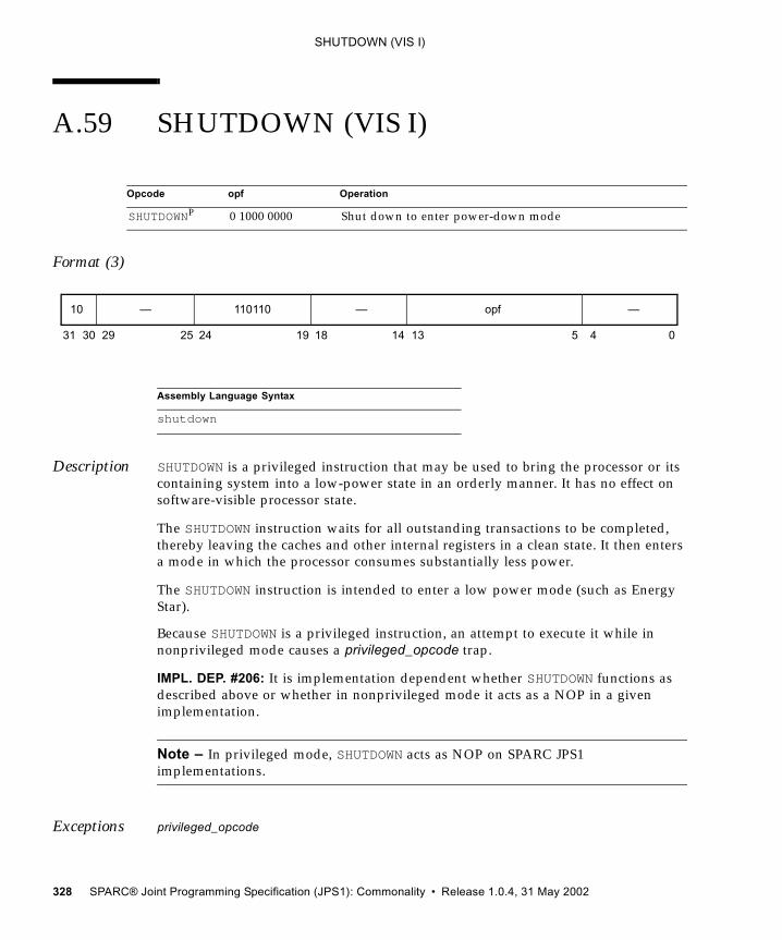
SHUTDOWN (VIS I)
A.59 SHUTDOWN (VIS I)
Format (3)
Description SHUTDOWN is a privileged instruction that may be used to bring the processor or its containing system into a low-power state in an orderly manner. It has no effect on software-visible processor state.
The SHUTDOWN instruction waits for all outstanding transactions to be completed, thereby leaving the caches and other internal registers in a clean state. It then enters a mode in which the processor consumes substantially less power.
The SHUTDOWN instruction is intended to enter a low power mode (such as Energy Star).
Because SHUTDOWN is a privileged instruction, an attempt to execute it while in nonprivileged mode causes a privileged_opcode trap.
IMPL. DEP. #206: It is implementation dependent whether SHUTDOWN functions as described above or whether in nonprivileged mode it acts as a NOP in a given implementation.
Note – In privileged mode, SHUTDOWN acts as NOP on SPARC JPS1 implementations.
Exceptions privileged_opcode
Opcode opf Operation
SHUTDOWNP 0 1000 0000 Shut down to enter power-down mode
Assembly Language Syntax
shutdown
31 24 02530 29 19 18 14 13 5 4
—10 110110 opf— —
328 SPARC® Joint Programming Specification (JPS1): Commonality • Release 1.0.4, 31 May 2002
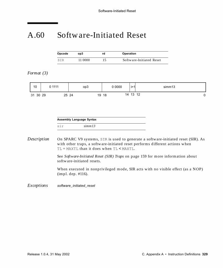
Software-Initiated Reset
A.60 Software-Initiated Reset
Format (3)
Description On SPARC V9 systems, SIR is used to generate a software-initiated reset (SIR). As with other traps, a software-initiated reset performs different actions when TL = MAXTL than it does when TL < MAXTL.
See Software-Initiated Reset (SIR) Traps on page 159 for more information about software-initiated resets.
When executed in nonprivileged mode, SIR acts with no visible effect (as a NOP) (impl. dep. #116).
Exceptions software_initiated_reset
Opcode op3 rd Operation
SIR 11 0000 15 Software-Initiated Reset
Assembly Language Syntax
sir simm13
31 1924 18 02530 29
10 0 1111 op3
14 13
0 0000 simm13
12
i=1
Release 1.0.4, 31 May 2002 C. Appendix A • Instruction Definitions 329
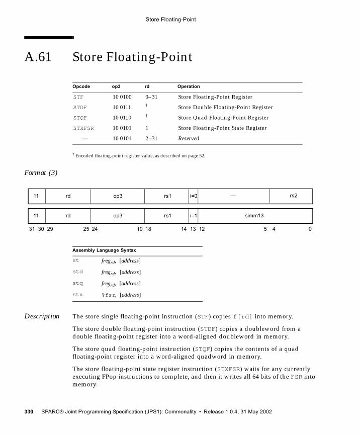
Store Floating-Point
A.61 Store Floating-Point
† Encoded floating-point register value, as described on page 52.
Format (3)
Description The store single floating-point instruction (STF) copies f[rd] into memory.
The store double floating-point instruction (STDF) copies a doubleword from a double floating-point register into a word-aligned doubleword in memory.
The store quad floating-point instruction (STQF) copies the contents of a quad floating-point register into a word-aligned quadword in memory.
The store floating-point state register instruction (STXFSR) waits for any currently executing FPop instructions to complete, and then it writes all 64 bits of the FSR into memory.
Opcode op3 rd Operation
STF 10 0100 0–31 Store Floating-Point Register
STDF 10 0111 † Store Double Floating-Point Register
STQF 10 0110 † Store Quad Floating-Point Register
STXFSR 10 0101 1 Store Floating-Point State Register
— 10 0101 2–31 Reserved
Assembly Language Syntax
st fregrd, [address]
std fregrd, [address]
stq fregrd, [address]
stx %fsr, [address]
31 24 02530 29 19 18 14 13 12 5 4
rd11 op3 rs1 simm13i=1
rd11 op3 rs1 i=0 — rs2
330 SPARC® Joint Programming Specification (JPS1): Commonality • Release 1.0.4, 31 May 2002
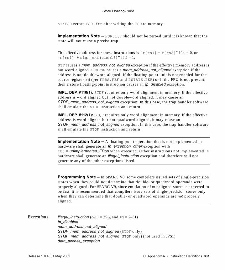
Store Floating-Point
STXFSR zeroes FSR.ftt after writing the FSR to memory.
Implementation Note – FSR.ftt should not be zeroed until it is known that the store will not cause a precise trap.
The effective address for these instructions is “r[rs1] + r[rs2]” if i = 0, or “r[rs1] + sign_ext(simm13)” if i = 1.
STF causes a mem_address_not_aligned exception if the effective memory address is not word aligned. STXFSR causes a mem_address_not_aligned exception if the address is not doubleword aligned. If the floating-point unit is not enabled for the source register rd (per FPRS.FEF and PSTATE.PEF) or if the FPU is not present, then a store floating-point instruction causes an fp_disabled exception.
IMPL. DEP. #110(1): STDF requires only word alignment in memory. If the effective address is word aligned but not doubleword aligned, it may cause an STDF_mem_address_not_aligned exception. In this case, the trap handler software shall emulate the STDF instruction and return.
IMPL. DEP. #112(1): STQF requires only word alignment in memory. If the effective address is word aligned but not quadword aligned, it may cause an STQF_mem_address_not_aligned exception. In this case, the trap handler software shall emulate the STQF instruction and return.
Implementation Note – A floating-point operation that is not implemented in hardware shall generate an fp_exception_other exception with ftt = unimplemented_FPop when executed. Other instructions not implemented in hardware shall generate an illegal_instruction exception and therefore will not generate any of the other exceptions listed.
Programming Note – In SPARC V8, some compilers issued sets of single-precision stores when they could not determine that double- or quadword operands were properly aligned. For SPARC V9, since emulation of misaligned stores is expected to be fast, it is recommended that compilers issue sets of single-precision stores only when they can determine that double- or quadword operands are not properly aligned.
Exceptions illegal_instruction (op3 = 2516 and rd = 2–31)fp_disabled mem_address_not_aligned STDF_mem_address_not_aligned (STDF only)STQF_mem_address_not_aligned (STQF only) (not used in JPS1)data_access_exception
Release 1.0.4, 31 May 2002 C. Appendix A • Instruction Definitions 331
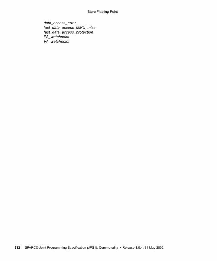
Store Floating-Point
data_access_errorfast_data_access_MMU_missfast_data_access_protectionPA_watchpointVA_watchpoint
332 SPARC® Joint Programming Specification (JPS1): Commonality • Release 1.0.4, 31 May 2002
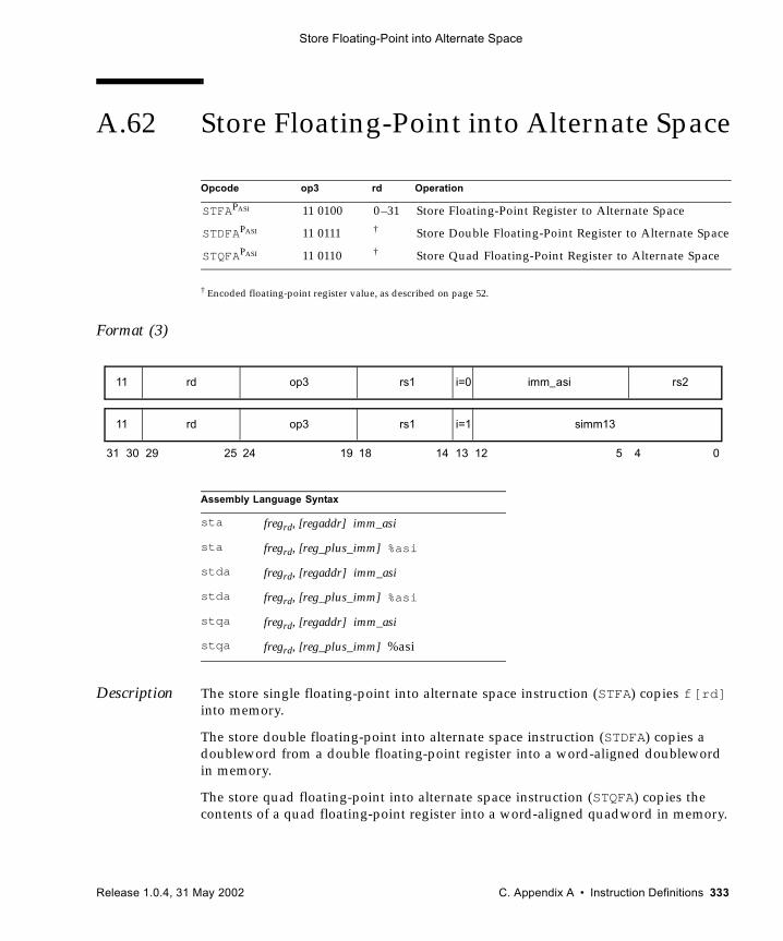
Store Floating-Point into Alternate Space
A.62 Store Floating-Point into Alternate Space
† Encoded floating-point register value, as described on page 52.
Format (3)
Description The store single floating-point into alternate space instruction (STFA) copies f[rd] into memory.
The store double floating-point into alternate space instruction (STDFA) copies a doubleword from a double floating-point register into a word-aligned doubleword in memory.
The store quad floating-point into alternate space instruction (STQFA) copies the contents of a quad floating-point register into a word-aligned quadword in memory.
Opcode op3 rd Operation
STFAPASI 11 0100 0–31 Store Floating-Point Register to Alternate Space
STDFAPASI 11 0111 † Store Double Floating-Point Register to Alternate Space
STQFAPASI 11 0110 † Store Quad Floating-Point Register to Alternate Space
Assembly Language Syntax
sta fregrd, [regaddr] imm_asi
sta fregrd, [reg_plus_imm] %asi
stda fregrd, [regaddr] imm_asi
stda fregrd, [reg_plus_imm] %asi
stqa fregrd, [regaddr] imm_asi
stqa fregrd, [reg_plus_imm] %asi
31 24 02530 29 19 18
rd11 op3 imm_asi
14 13 12 5 4
rs1 rs2i=0
rd11 op3 rs1 simm13i=1
Release 1.0.4, 31 May 2002 C. Appendix A • Instruction Definitions 333
Store Floating-Point into Alternate Space
Store floating-point into alternate space instructions contain the address space identifier (ASI) to be used for the load in the imm_asi field if i = 0 or in the ASI register if i = 1. The access is privileged if bit 7 of the ASI is 0; otherwise, it is not privileged. The effective address for these instructions is “r[rs1] + r[rs2]” if i = 0, or “r[rs1] + sign_ext(simm13)” if i = 1.
STFA causes a mem_address_not_aligned exception if the effective memory address is not word aligned. If the floating-point unit is not enabled for the source register rd (per FPRS.FEF and PSTATE.PEF) or if the FPU is not present, store floating-point into alternate space instructions cause an fp_disabled exception.
Implementation Notes – This check is not made for STQFA. STFA and STDFA cause a privileged_action exception if PSTATE.PRIV = 0 and bit 7 of the ASI is 0.
STDFA with certain target ASIs is defined to be a 64-byte block-store instruction. See Block Load and Store (VIS I) on page 199 for details.
STDFA with certain target ASIs is defined to be a Partial Store instruction. See Partial Store (VIS I) on page 282 for details.
STDFA with certain target ASIs is defined to be a Short Floating-point Store instruction. See Short Floating-Point Load and Store (VIS I) on page 326 for details.
IMPL. DEP. #110(2): STDFA requires only word alignment in memory. If the effective address is word aligned but not doubleword aligned, it may cause an STDF_mem_address_not_aligned exception. In this case, the trap handler software shall emulate the STDFA instruction and return.
IMPL. DEP. #112(2): STQFA requires only word alignment in memory. If the effective address is word aligned but not quadword aligned, it may cause an STQF_mem_address_not_aligned exception. In this case, the trap handler software shall emulate the STQFA instruction and return.
Programming Note – In SPARC V8, some compilers issued sets of single-precision stores when they could not determine that double- or quadword operands were properly aligned. For SPARC V9, since emulation of misaligned stores is expected to be fast, we recommend that compilers issue sets of single-precision stores only when they can determine that double- or quadword operands are not properly aligned.
Exceptions fp_disabled mem_address_not_aligned STDF_mem_address_not_aligned (STDFA only)STQF_mem_address_not_aligned (STQFA only) (not used in JPS1)privileged_action data_access_exception
334 SPARC® Joint Programming Specification (JPS1): Commonality • Release 1.0.4, 31 May 2002
Store Floating-Point into Alternate Space
data_access_errorfast_data_access_MMU_missfast_data_access_protectionPA_watchpointVA_watchpoint
Release 1.0.4, 31 May 2002 C. Appendix A • Instruction Definitions 335
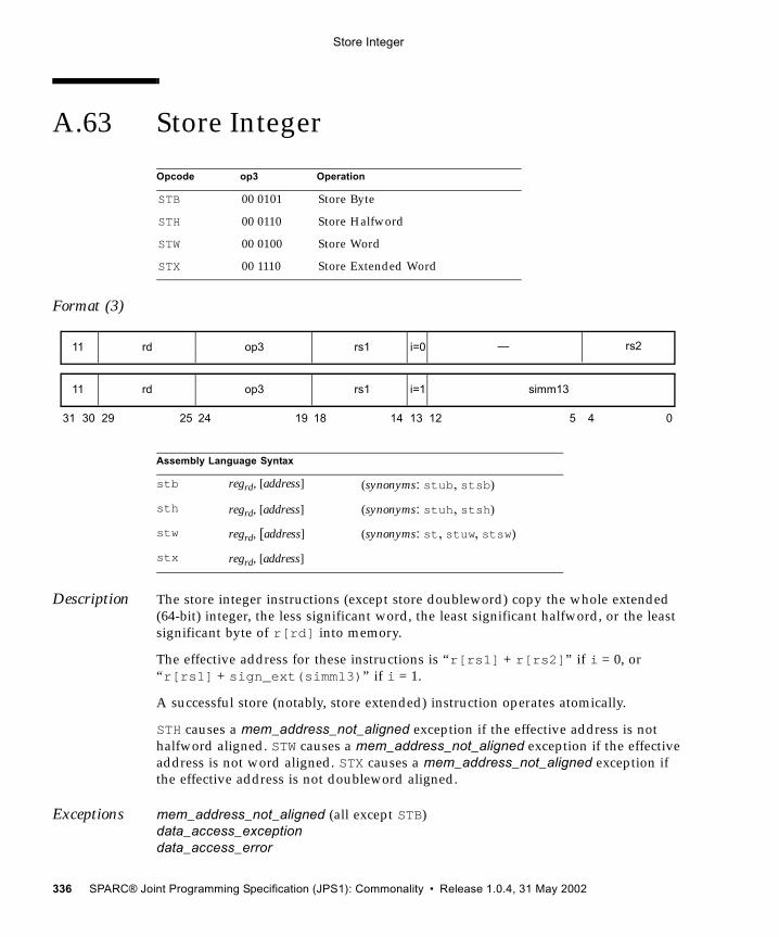
Store Integer
A.63 Store Integer
Format (3)
Description The store integer instructions (except store doubleword) copy the whole extended (64-bit) integer, the less significant word, the least significant halfword, or the least significant byte of r[rd] into memory.
The effective address for these instructions is “r[rs1] + r[rs2]” if i = 0, or “r[rs1] + sign_ext(simm13)” if i = 1.
A successful store (notably, store extended) instruction operates atomically.
STH causes a mem_address_not_aligned exception if the effective address is not halfword aligned. STW causes a mem_address_not_aligned exception if the effective address is not word aligned. STX causes a mem_address_not_aligned exception if the effective address is not doubleword aligned.
Exceptions mem_address_not_aligned (all except STB)data_access_exceptiondata_access_error
Opcode op3 Operation
STB 00 0101 Store Byte
STH 00 0110 Store Halfword
STW 00 0100 Store Word
STX 00 1110 Store Extended Word
Assembly Language Syntax
stb regrd, [address] (synonyms: stub, stsb)
sth regrd, [address] (synonyms: stuh, stsh)
stw regrd, [address] (synonyms: st, stuw, stsw)
stx regrd, [address]
31 24 02530 29 19 18 14 13 12 5 4
rd11 op3 rs1 simm13i=1
rd11 op3 rs1 i=0 — rs2
336 SPARC® Joint Programming Specification (JPS1): Commonality • Release 1.0.4, 31 May 2002
Store Integer
fast_data_access_MMU_missfast_data_access_protectionPA_watchpointVA_watchpoint
Release 1.0.4, 31 May 2002 C. Appendix A • Instruction Definitions 337
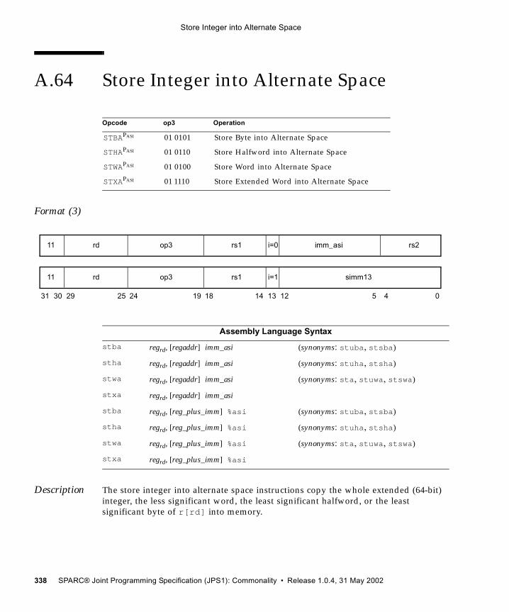
Store Integer into Alternate Space
A.64 Store Integer into Alternate Space
Format (3)
Description The store integer into alternate space instructions copy the whole extended (64-bit) integer, the less significant word, the least significant halfword, or the least significant byte of r[rd] into memory.
Opcode op3 Operation
STBAPASI 01 0101 Store Byte into Alternate Space
STHAPASI 01 0110 Store Halfword into Alternate Space
STWAPASI 01 0100 Store Word into Alternate Space
STXAPASI 01 1110 Store Extended Word into Alternate Space
Assembly Language Syntax
stba regrd, [regaddr] imm_asi (synonyms: stuba, stsba)
stha regrd, [regaddr] imm_asi (synonyms: stuha, stsha)
stwa regrd, [regaddr] imm_asi (synonyms: sta, stuwa, stswa)
stxa regrd, [regaddr] imm_asi
stba regrd, [reg_plus_imm] %asi (synonyms: stuba, stsba)
stha regrd, [reg_plus_imm] %asi (synonyms: stuha, stsha)
stwa regrd, [reg_plus_imm] %asi (synonyms: sta, stuwa, stswa)
stxa regrd, [reg_plus_imm] %asi
31 24 02530 29 19 18
rd11 op3 imm_asi
14 13 12 5 4
rs1 rs2i=0
rd11 op3 rs1 simm13i=1
338 SPARC® Joint Programming Specification (JPS1): Commonality • Release 1.0.4, 31 May 2002
Store Integer into Alternate Space
Store integer to alternate space instructions contain the address space identifier (ASI) to be used for the store in the imm_asi field if i = 0, or in the ASI register if i = 1. The access is privileged if bit 7 of the ASI is 0; otherwise, it is not privileged. The effective address for these instructions is “r[rs1] + r[rs2]” if i = 0, or “r[rs1]+sign_ext(simm13)” if i = 1.
A successful store (notably, store extended) instruction operates atomically.
STHA causes a mem_address_not_aligned exception if the effective address is not halfword aligned. STWA causes a mem_address_not_aligned exception if the effective address is not word aligned. STXA causes a mem_address_not_aligned exception if the effective address is not doubleword aligned.
A store integer into alternate space instruction causes a privileged_action exception if PSTATE.PRIV = 0 and bit 7 of the ASI is 0.
Compatibility Note – The SPARC V8 STA instruction is renamed STWA in SPARC V9.
Exceptions privileged_action mem_address_not_aligned (all except STBA)data_access_exceptiondata_access_errorfast_data_access_MMU_missfast_data_access_protectionPA_watchpointVA_watchpoint
Release 1.0.4, 31 May 2002 C. Appendix A • Instruction Definitions 339
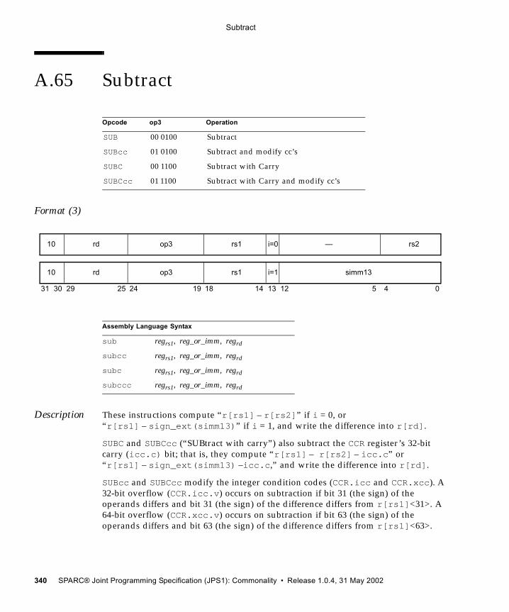
Subtract
A.65 Subtract
Format (3)
Description These instructions compute “r[rs1] – r[rs2]” if i = 0, or “r[rs1] – sign_ext(simm13)” if i = 1, and write the difference into r[rd].
SUBC and SUBCcc (“SUBtract with carry”) also subtract the CCR register’s 32-bit carry (icc.c) bit; that is, they compute “r[rs1] – r[rs2] – icc.c” or “r[rs1] – sign_ext(simm13) –icc.c,” and write the difference into r[rd].
SUBcc and SUBCcc modify the integer condition codes (CCR.icc and CCR.xcc). A 32-bit overflow (CCR.icc.v) occurs on subtraction if bit 31 (the sign) of the operands differs and bit 31 (the sign) of the difference differs from r[rs1]<31>. A 64-bit overflow (CCR.xcc.v) occurs on subtraction if bit 63 (the sign) of the operands differs and bit 63 (the sign) of the difference differs from r[rs1]<63>.
Opcode op3 Operation
SUB 00 0100 Subtract
SUBcc 01 0100 Subtract and modify cc’s
SUBC 00 1100 Subtract with Carry
SUBCcc 01 1100 Subtract with Carry and modify cc’s
Assembly Language Syntax
sub regrs1, reg_or_imm, regrd
subcc regrs1, reg_or_imm, regrd
subc regrs1, reg_or_imm, regrd
subccc regrs1, reg_or_imm, regrd
31 24 02530 29 19 18
rd10 op3 —
14 13 12 5 4
rs1 rs2i=0
rd10 op3 rs1 simm13i=1
340 SPARC® Joint Programming Specification (JPS1): Commonality • Release 1.0.4, 31 May 2002
Subtract
Programming Notes– A SUBcc with rd = 0 can be used to effect a signed or unsigned integer comparison. See the CMP synthetic instruction in Appendix G, Assembly Language Syntax.
SUBC and SUBCcc read the 32-bit condition codes’ carry bit (CCR.icc.c), not the 64-bit condition codes’ carry bit (CCR.xcc.c).
Exceptions None
Release 1.0.4, 31 May 2002 C. Appendix A • Instruction Definitions 341
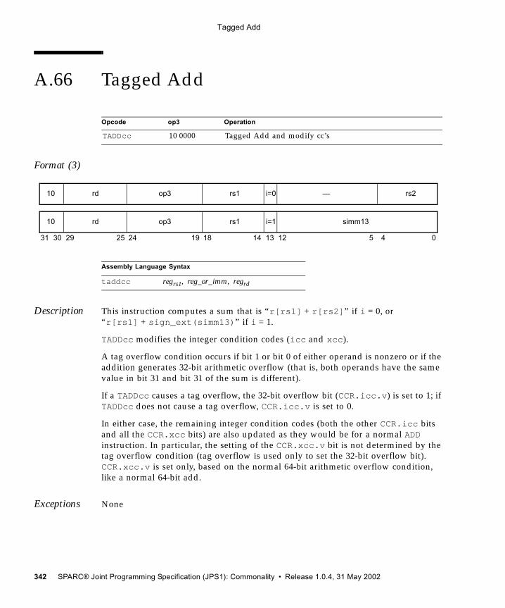
Tagged Add
A.66 Tagged Add
Format (3)
Description This instruction computes a sum that is “r[rs1] + r[rs2]” if i = 0, or “r[rs1] + sign_ext(simm13)” if i = 1.
TADDcc modifies the integer condition codes (icc and xcc).
A tag overflow condition occurs if bit 1 or bit 0 of either operand is nonzero or if the addition generates 32-bit arithmetic overflow (that is, both operands have the same value in bit 31 and bit 31 of the sum is different).
If a TADDcc causes a tag overflow, the 32-bit overflow bit (CCR.icc.v) is set to 1; if TADDcc does not cause a tag overflow, CCR.icc.v is set to 0.
In either case, the remaining integer condition codes (both the other CCR.icc bits and all the CCR.xcc bits) are also updated as they would be for a normal ADD instruction. In particular, the setting of the CCR.xcc.v bit is not determined by the tag overflow condition (tag overflow is used only to set the 32-bit overflow bit). CCR.xcc.v is set only, based on the normal 64-bit arithmetic overflow condition, like a normal 64-bit add.
Exceptions None
Opcode op3 Operation
TADDcc 10 0000 Tagged Add and modify cc’s
Assembly Language Syntax
taddcc regrs1, reg_or_imm, regrd
31 24 02530 29 19 18
rd10 op3 —
14 13 12 5 4
rs1 rs2i=0
rd10 op3 rs1 simm13i=1
342 SPARC® Joint Programming Specification (JPS1): Commonality • Release 1.0.4, 31 May 2002
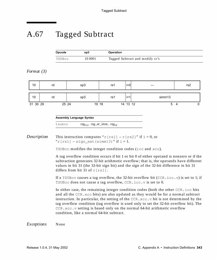
Tagged Subtract
A.67 Tagged Subtract
Format (3)
Description This instruction computes “r[rs1] – r[rs2]” if i = 0, or “r[rs1] – sign_ext(simm13)” if i = 1.
TSUBcc modifies the integer condition codes (icc and xcc).
A tag overflow condition occurs if bit 1 or bit 0 of either operand is nonzero or if the subtraction generates 32-bit arithmetic overflow; that is, the operands have different values in bit 31 (the 32-bit sign bit) and the sign of the 32-bit difference in bit 31 differs from bit 31 of r[rs1].
If a TSUBcc causes a tag overflow, the 32-bit overflow bit (CCR.icc.v) is set to 1; if TSUBcc does not cause a tag overflow, CCR.icc.v is set to 0.
In either case, the remaining integer condition codes (both the other CCR.icc bits and all the CCR.xcc bits) are also updated as they would be for a normal subtract instruction. In particular, the setting of the CCR.xcc.v bit is not determined by the tag overflow condition (tag overflow is used only to set the 32-bit overflow bit). The CCR.xcc.v setting is based only on the normal 64-bit arithmetic overflow condition, like a normal 64-bit subtract.
Exceptions None
Opcode op3 Operation
TSUBcc 10 0001 Tagged Subtract and modify cc’s
Assembly Language Syntax
tsubcc regrs1, reg_or_imm, regrd
31 24 02530 29 19 18
rd10 op3 —
14 13 12 5 4
rs1 rs2i=0
rd10 op3 rs1 simm13i=1
Release 1.0.4, 31 May 2002 C. Appendix A • Instruction Definitions 343
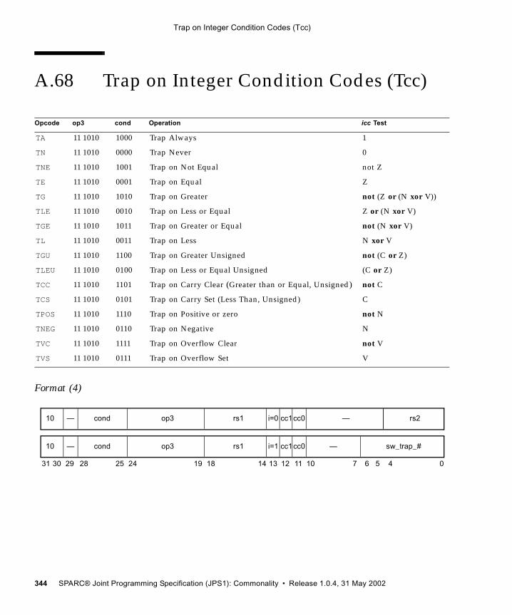
Trap on Integer Condition Codes (Tcc)
A.68 Trap on Integer Condition Codes (Tcc)
Format (4)
Opcode op3 cond Operation icc Test
TA 11 1010 1000 Trap Always 1
TN 11 1010 0000 Trap Never 0
TNE 11 1010 1001 Trap on Not Equal not Z
TE 11 1010 0001 Trap on Equal Z
TG 11 1010 1010 Trap on Greater not (Z or (N xor V))
TLE 11 1010 0010 Trap on Less or Equal Z or (N xor V)
TGE 11 1010 1011 Trap on Greater or Equal not (N xor V)
TL 11 1010 0011 Trap on Less N xor V
TGU 11 1010 1100 Trap on Greater Unsigned not (C or Z)
TLEU 11 1010 0100 Trap on Less or Equal Unsigned (C or Z)
TCC 11 1010 1101 Trap on Carry Clear (Greater than or Equal, Unsigned) not C
TCS 11 1010 0101 Trap on Carry Set (Less Than, Unsigned) C
TPOS 11 1010 1110 Trap on Positive or zero not N
TNEG 11 1010 0110 Trap on Negative N
TVC 11 1010 1111 Trap on Overflow Clear not V
TVS 11 1010 0111 Trap on Overflow Set V
5 4
10 cond op3 rs1 i=0 — rs2
31 141924 18 13 12 02530 29
—
28 7 6
cc1cc0
11 10
10 cond op3 rs1 i=1 —— cc1cc0 sw_trap_#
344 SPARC® Joint Programming Specification (JPS1): Commonality • Release 1.0.4, 31 May 2002
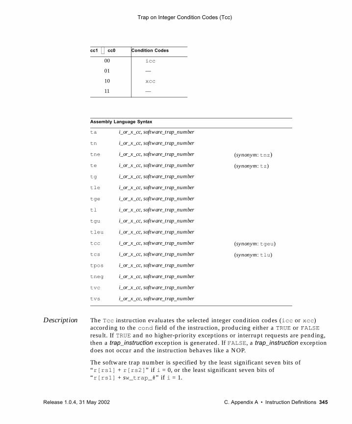
Trap on Integer Condition Codes (Tcc)
Description The Tcc instruction evaluates the selected integer condition codes (icc or xcc) according to the cond field of the instruction, producing either a TRUE or FALSE result. If TRUE and no higher-priority exceptions or interrupt requests are pending, then a trap_instruction exception is generated. If FALSE, a trap_instruction exception does not occur and the instruction behaves like a NOP.
The software trap number is specified by the least significant seven bits of “r[rs1] + r[rs2]” if i = 0, or the least significant seven bits of “r[rs1] + sw_trap_#” if i = 1.
cc1 cc0 Condition Codes
00 icc
01 —
10 xcc
11 —
Assembly Language Syntax
ta i_or_x_cc, software_trap_number
tn i_or_x_cc, software_trap_number
tne i_or_x_cc, software_trap_number (synonym: tnz)
te i_or_x_cc, software_trap_number (synonym: tz)
tg i_or_x_cc, software_trap_number
tle i_or_x_cc, software_trap_number
tge i_or_x_cc, software_trap_number
tl i_or_x_cc, software_trap_number
tgu i_or_x_cc, software_trap_number
tleu i_or_x_cc, software_trap_number
tcc i_or_x_cc, software_trap_number (synonym: tgeu)
tcs i_or_x_cc, software_trap_number (synonym: tlu)
tpos i_or_x_cc, software_trap_number
tneg i_or_x_cc, software_trap_number
tvc i_or_x_cc, software_trap_number
tvs i_or_x_cc, software_trap_number
Release 1.0.4, 31 May 2002 C. Appendix A • Instruction Definitions 345
Trap on Integer Condition Codes (Tcc)
When i = 1, bits 7 through 10 are reserved and should be supplied as zeroes by software. When i = 0, bits 5 through 10 are reserved, the most significant 57 bits of “r[rs1] + r[rs2]” are unused, and both should be supplied as zeroes by software.
Description (Effect on Privileged State)
If a trap_instruction traps, 256 plus the software trap number is written into TT[TL]. Then the trap is taken, and the processor performs the normal trap entry procedure, as described in Chapter 7, Traps.
Programming Note – Tcc can be used to implement breakpointing, tracing, and calls to supervisor software. It can also be used for runtime checks, such as out-of-range array indexes, integer overflow, and so on.
Compatibility Note – Tcc is upward compatible with the SPARC V8 Ticc instruction, with one qualification: a Ticc with i = 1 and simm13 < 0 may execute differently on a SPARC V9 processor. Use of the i = 1 form of Ticc is believed to be rare in SPARC V8 software, and simm13 < 0 is probably not used at all, so it is believed that, in practice, full software compatibility will be achieved.
Exceptions trap_instructionillegal_instruction (cc1 cc0 = 012 or 112, or reserved fields nonzero)
346 SPARC® Joint Programming Specification (JPS1): Commonality • Release 1.0.4, 31 May 2002
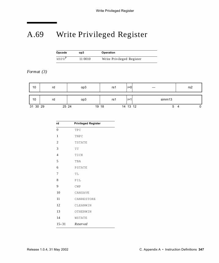
Write Privileged Register
A.69 Write Privileged Register
Format (3)
Opcode op3 Operation
WRPRP 11 0010 Write Privileged Register
rd Privileged Register
0 TPC
1 TNPC
2 TSTATE
3 TT
4 TICK
5 TBA
6 PSTATE
7 TL
8 PIL
9 CWP
10 CANSAVE
11 CANRESTORE
12 CLEANWIN
13 OTHERWIN
14 WSTATE
15–31 Reserved
31 24 02530 29 19 18
rd10 op3 —
14 13 12 5 4
rs1 rs2i=0
rd10 op3 rs1 simm13i=1
Release 1.0.4, 31 May 2002 C. Appendix A • Instruction Definitions 347
Write Privileged Register
Description This instruction stores the value “r[rs1] xor r[rs2]” if i = 0, or “r[rs1] xor sign_ext(simm13)” if i = 1 to the writable fields of the specified privileged state register. Note: The operation is exclusive-or.
The rd field in the instruction determines the privileged register that is written. There are at least four copies of the TPC, TNPC, TT, and TSTATE registers, one for each trap level. A write to one of these registers sets the register indexed by the current value in the trap-level register (TL). A write to TPC, TNPC, TT, or TSTATE when the trap level is zero (TL = 0) causes an illegal_instruction exception.
A WRPR of TL does not cause a trap or return from trap; it does not alter any other machine state.
Programming Note – A WRPR of TL can be used to read the values of TPC, TNPC, and TSTATE for any trap level; however, take care that traps do not occur while the TL register is modified.
The WRPR instruction is a non-delayed-write instruction. The instruction immediately following the WRPR observes any changes made to processor state made by the WRPR.
Assembly Language Syntax
wrpr regrs1, reg_or_imm, %tpc
wrpr regrs1, reg_or_imm, %tnpc
wrpr regrs1, reg_or_imm, %tstate
wrpr regrs1, reg_or_imm, %tt
wrpr regrs1, reg_or_imm, %tick
wrpr regrs1, reg_or_imm, %tba
wrpr regrs1, reg_or_imm, %pstate
wrpr regrs1, reg_or_imm, %tl
wrpr regrs1, reg_or_imm, %pil
wrpr regrs1, reg_or_imm, %cwp
wrpr regrs1, reg_or_imm, %cansave
wrpr regrs1, reg_or_imm, %canrestore
wrpr regrs1, reg_or_imm, %cleanwin
wrpr regrs1, reg_or_imm, %otherwin
wrpr regrs1, reg_or_imm, %wstate
348 SPARC® Joint Programming Specification (JPS1): Commonality • Release 1.0.4, 31 May 2002
Write Privileged Register
WRPR instructions with rd in the range 15–31 are reserved for future versions of the architecture; executing a WRPR instruction with rd in that range causes an illegal_instruction exception.
Implementation Note – Some WRPR instructions could serialize the processor in some implementations. See specific Implementation Supplements for applicability and details.
Exceptions privileged_opcodeillegal_instruction ((rd = 15–31) or ((rd ≤ 3) and (TL = 0)))
Release 1.0.4, 31 May 2002 C. Appendix A • Instruction Definitions 349
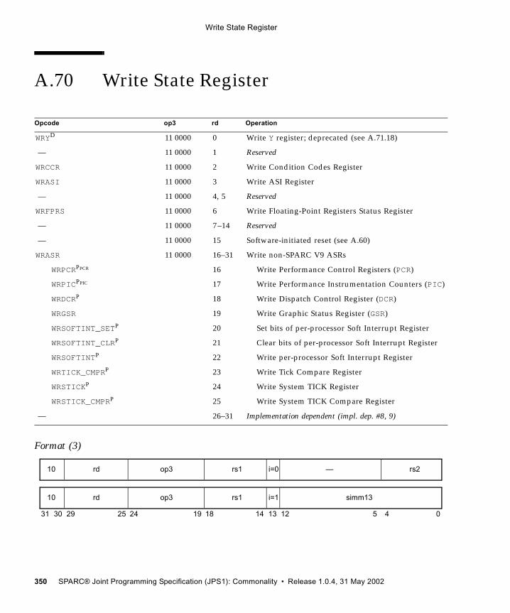
Write State Register
A.70 Write State Register
Format (3)
Opcode op3 rd Operation
WRYD 11 0000 0 Write Y register; deprecated (see A.71.18)
— 11 0000 1 Reserved
WRCCR 11 0000 2 Write Condition Codes Register
WRASI 11 0000 3 Write ASI Register
— 11 0000 4, 5 Reserved
WRFPRS 11 0000 6 Write Floating-Point Registers Status Register
— 11 0000 7–14 Reserved
— 11 0000 15 Software-initiated reset (see A.60)
WRASR 11 0000 16–31 Write non-SPARC V9 ASRs
WRPCRPPCR 16 Write Performance Control Registers (PCR)
WRPICPPIC 17 Write Performance Instrumentation Counters (PIC)
WRDCRP 18 Write Dispatch Control Register (DCR)
WRGSR 19 Write Graphic Status Register (GSR)
WRSOFTINT_SETP 20 Set bits of per-processor Soft Interrupt Register
WRSOFTINT_CLRP 21 Clear bits of per-processor Soft Interrupt Register
WRSOFTINTP 22 Write per-processor Soft Interrupt Register
WRTICK_CMPRP 23 Write Tick Compare Register
WRSTICKP 24 Write System TICK Register
WRSTICK_CMPRP 25 Write System TICK Compare Register
— 26–31 Implementation dependent (impl. dep. #8, 9)
31 24 02530 29 19 18
rd10 op3 —
14 13 12 5 4
rs1 rs2i=0
rd10 op3 rs1 simm13i=1
350 SPARC® Joint Programming Specification (JPS1): Commonality • Release 1.0.4, 31 May 2002
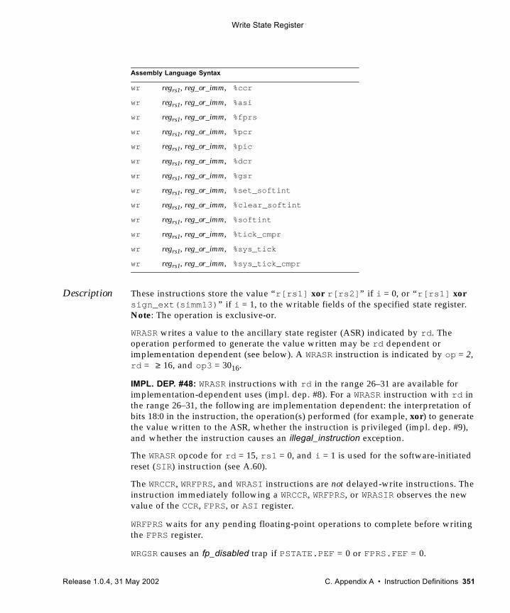
Write State Register
Description These instructions store the value “r[rs1] xor r[rs2]” if i = 0, or “r[rs1] xor sign_ext(simm13)” if i = 1, to the writable fields of the specified state register. Note: The operation is exclusive-or.
WRASR writes a value to the ancillary state register (ASR) indicated by rd. The operation performed to generate the value written may be rd dependent or implementation dependent (see below). A WRASR instruction is indicated by op = 2, rd = ≥ 16, and op3 = 3016.
IMPL. DEP. #48: WRASR instructions with rd in the range 26–31 are available for implementation-dependent uses (impl. dep. #8). For a WRASR instruction with rd in the range 26–31, the following are implementation dependent: the interpretation of bits 18:0 in the instruction, the operation(s) performed (for example, xor) to generate the value written to the ASR, whether the instruction is privileged (impl. dep. #9), and whether the instruction causes an illegal_instruction exception.
The WRASR opcode for rd = 15, rs1 = 0, and i = 1 is used for the software-initiated reset (SIR) instruction (see A.60).
The WRCCR, WRFPRS, and WRASI instructions are not delayed-write instructions. The instruction immediately following a WRCCR, WRFPRS, or WRASIR observes the new value of the CCR, FPRS, or ASI register.
WRFPRS waits for any pending floating-point operations to complete before writing the FPRS register.
WRGSR causes an fp_disabled trap if PSTATE.PEF = 0 or FPRS.FEF = 0.
Assembly Language Syntax
wr regrs1, reg_or_imm, %ccr
wr regrs1, reg_or_imm, %asi
wr regrs1, reg_or_imm, %fprs
wr regrs1, reg_or_imm, %pcr
wr regrs1, reg_or_imm, %pic
wr regrs1, reg_or_imm, %dcr
wr regrs1, reg_or_imm, %gsr
wr regrs1, reg_or_imm, %set_softint
wr regrs1, reg_or_imm, %clear_softint
wr regrs1, reg_or_imm, %softint
wr regrs1, reg_or_imm, %tick_cmpr
wr regrs1, reg_or_imm, %sys_tick
wr regrs1, reg_or_imm, %sys_tick_cmpr
Release 1.0.4, 31 May 2002 C. Appendix A • Instruction Definitions 351
Write State Register
WRPIC causes a privileged_action exception if PSTATE.PRIV = 0 and PCR.PRIV = 1.
WRPCR causes an exception due to access privilege violation under implementation-dependent circumstances (impl. dep. #250).
See Ancillary State Registers (ASRs) on page 83 for details of the ASR registers.
Note – See I.1, Read/Write Ancillary State Registers (ASRs), for a discussion of extending the SPARC V9 instruction set by means of read/write ASR instructions.
Implementation Note – Ancillary state registers may include (for example) timer, counter, diagnostic, self-test, and trap-control registers.
Compatibility Note – The SPARC V8 WRIER, WRPSR, WRWIM, and WRTBR instructions do not exist in SPARC V9 because the IER, PSR, TBR, and WIM registers do not exist in SPARC V9.
Implementation Note – Some WRASR instructions could serialize the processor in some implementations. See specific Implementation Supplements for applicability and details.
Exceptions software_initiated_reset (rd = 15, rs1 = 0, and i = 1 only)privileged_opcode (WRDCR, WRSOFTINT_SET, WRSOFTINT_CLR, WRSOFTINT, WRTICK_CMPR, WRSTICK, WRSTICK_CMPR, and WRPCR (impl. dep. #250))illegal_instruction (WRASR with rd = 1, 4, 5, 7–14, 26-31;
WRASR with rd = 15 and rs1 ≠ 0 or i ≠ 1)privileged_action (WRPIC with PSTATE.PRIV = 0 and PCR.PRIV = 1, WRPCR (impl. dep. #250))fp_disabled (WRGSR with PSTATE.PEF = 0 or FPRS.FEF = 0)
352 SPARC® Joint Programming Specification (JPS1): Commonality • Release 1.0.4, 31 May 2002
Deprecated Instructions
A.71 Deprecated InstructionsThe following instructions are deprecated; they are provided only for compatibility with previous versions of the architecture. They should not be used in new SPARC V9 software. For each deprecated instruction, we recommend the instruction to be used instead. Please see TABLE A-2 on page 186 for the page number at which you can find a description of the preferred instruction.
Release 1.0.4, 31 May 2002 C. Appendix A • Instruction Definitions 353
Deprecated Instructions
354 SPARC® Joint Programming Specification (JPS1): Commonality • Release 1.0.4, 31 May 2002
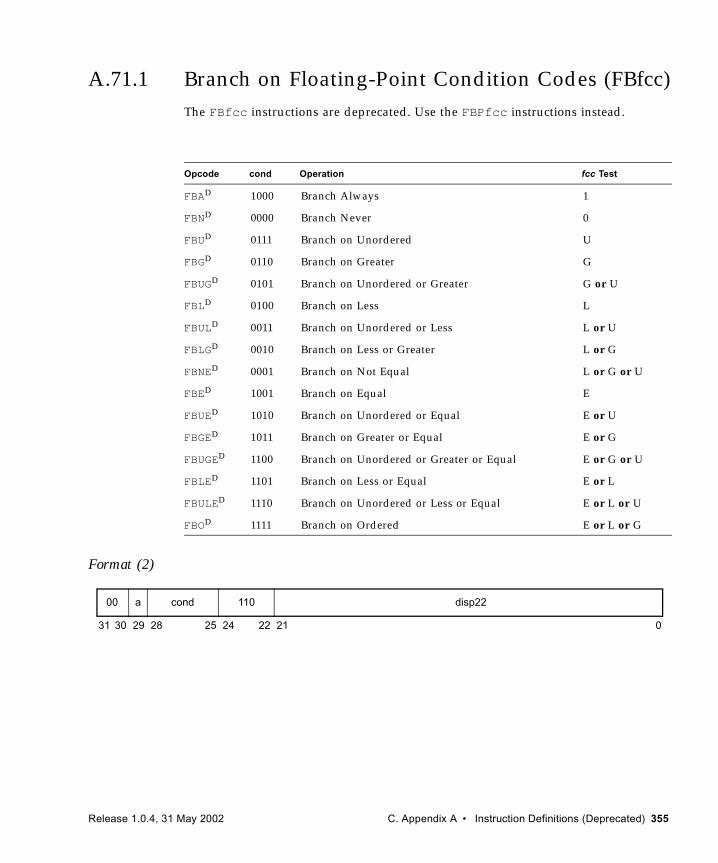
A.71.1 Branch on Floating-Point Condition Codes (FBfcc)The FBfcc instructions are deprecated. Use the FBPfcc instructions instead.
Format (2)
Opcode cond Operation fcc Test
FBAD 1000 Branch Always 1
FBND 0000 Branch Never 0
FBUD 0111 Branch on Unordered U
FBGD 0110 Branch on Greater G
FBUGD 0101 Branch on Unordered or Greater G or U
FBLD 0100 Branch on Less L
FBULD 0011 Branch on Unordered or Less L or U
FBLGD 0010 Branch on Less or Greater L or G
FBNED 0001 Branch on Not Equal L or G or U
FBED 1001 Branch on Equal E
FBUED 1010 Branch on Unordered or Equal E or U
FBGED 1011 Branch on Greater or Equal E or G
FBUGED 1100 Branch on Unordered or Greater or Equal E or G or U
FBLED 1101 Branch on Less or Equal E or L
FBULED 1110 Branch on Unordered or Less or Equal E or L or U
FBOD 1111 Branch on Ordered E or L or G
31 24 02530 29 28 22 21
cond00 a 110 disp22
Release 1.0.4, 31 May 2002 C. Appendix A • Instruction Definitions (Deprecated) 355
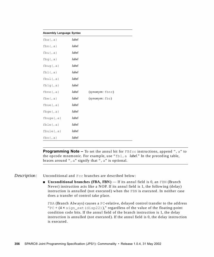
Programming Note – To set the annul bit for FBfcc instructions, append “,a” to the opcode mnemonic. For example, use “fbl,a label.” In the preceding table, braces around “,a” signify that “,a” is optional.
Description: Unconditional and Fcc branches are described below:
■ Unconditional branches (FBA, FBN) — If its annul field is 0, an FBN (Branch Never) instruction acts like a NOP. If its annul field is 1, the following (delay) instruction is annulled (not executed) when the FBN is executed. In neither case does a transfer of control take place.
FBA (Branch Always) causes a PC-relative, delayed control transfer to the address “PC + (4 × sign_ext(disp22)),” regardless of the value of the floating-point condition code bits. If the annul field of the branch instruction is 1, the delay instruction is annulled (not executed). If the annul field is 0, the delay instruction is executed.
Assembly Language Syntax
fba{,a} label
fbn{,a} label
fbu{,a} label
fbg{,a} label
fbug{,a} label
fbl{,a} label
fbul{,a} label
fblg{,a} label
fbne{,a} label (synonym: fbnz)
fbe{,a} label (synonym: fbz)
fbue{,a} label
fbge{,a} label
fbuge{,a} label
fble{,a} label
fbule{,a} label
fbo{,a} label
356 SPARC® Joint Programming Specification (JPS1): Commonality • Release 1.0.4, 31 May 2002
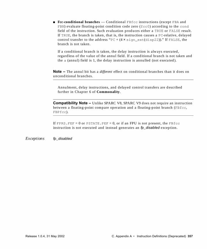
■ Fcc-conditional branches — Conditional FBfcc instructions (except FBA and FBN) evaluate floating-point condition code zero (fcc0) according to the cond field of the instruction. Such evaluation produces either a TRUE or FALSE result. If TRUE, the branch is taken, that is, the instruction causes a PC-relative, delayed control transfer to the address “PC + (4 × sign_ext(disp22)).” If FALSE, the branch is not taken.
If a conditional branch is taken, the delay instruction is always executed, regardless of the value of the annul field. If a conditional branch is not taken and the a (annul) field is 1, the delay instruction is annulled (not executed).
Note – The annul bit has a different effect on conditional branches than it does on unconditional branches.
Annulment, delay instructions, and delayed control transfers are described further in Chapter 6 of Commonality.
Compatibility Note – Unlike SPARC V8, SPARC V9 does not require an instruction between a floating-point compare operation and a floating-point branch (FBfcc, FBPfcc).
If FPRS.FEF = 0 or PSTATE.PEF = 0, or if an FPU is not present, the FBfcc instruction is not executed and instead generates an fp_disabled exception.
Exceptions fp_disabled
Release 1.0.4, 31 May 2002 C. Appendix A • Instruction Definitions (Deprecated) 357
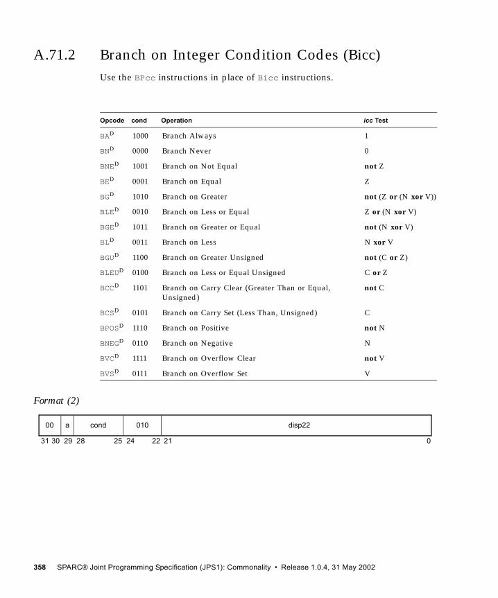
A.71.2 Branch on Integer Condition Codes (Bicc)Use the BPcc instructions in place of Bicc instructions.
Format (2)
Opcode cond Operation icc Test
BAD 1000 Branch Always 1
BND 0000 Branch Never 0
BNED 1001 Branch on Not Equal not Z
BED 0001 Branch on Equal Z
BGD 1010 Branch on Greater not (Z or (N xor V))
BLED 0010 Branch on Less or Equal Z or (N xor V)
BGED 1011 Branch on Greater or Equal not (N xor V)
BLD 0011 Branch on Less N xor V
BGUD 1100 Branch on Greater Unsigned not (C or Z)
BLEUD 0100 Branch on Less or Equal Unsigned C or Z
BCCD 1101 Branch on Carry Clear (Greater Than or Equal, Unsigned)
not C
BCSD 0101 Branch on Carry Set (Less Than, Unsigned) C
BPOSD 1110 Branch on Positive not N
BNEGD 0110 Branch on Negative N
BVCD 1111 Branch on Overflow Clear not V
BVSD 0111 Branch on Overflow Set V
31 24 02530 29 28 22 21
00 a cond 010 disp22
358 SPARC® Joint Programming Specification (JPS1): Commonality • Release 1.0.4, 31 May 2002
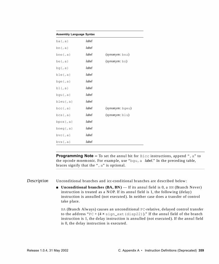
Programming Note – To set the annul bit for Bicc instructions, append “,a” to the opcode mnemonic. For example, use “bgu,a label.” In the preceding table, braces signify that the “,a” is optional.
Description Unconditional branches and icc-conditional branches are described below:
■ Unconditional branches (BA, BN) — If its annul field is 0, a BN (Branch Never) instruction is treated as a NOP. If its annul field is 1, the following (delay) instruction is annulled (not executed). In neither case does a transfer of control take place.
BA (Branch Always) causes an unconditional PC-relative, delayed control transfer to the address “PC + (4 × sign_ext(disp22)).” If the annul field of the branch instruction is 1, the delay instruction is annulled (not executed). If the annul field is 0, the delay instruction is executed.
Assembly Language Syntax
ba{,a} label
bn{,a} label
bne{,a} label (synonym: bnz)
be{,a} label (synonym: bz)
bg{,a} label
ble{,a} label
bge{,a} label
bl{,a} label
bgu{,a} label
bleu{,a} label
bcc{,a} label (synonym: bgeu)
bcs{,a} label (synonym: blu)
bpos{,a} label
bneg{,a} label
bvc{,a} label
bvs{,a} label
Release 1.0.4, 31 May 2002 C. Appendix A • Instruction Definitions (Deprecated) 359
■ Icc-conditional branches — Conditional Bicc instructions (all except BA and BN) evaluate the 32-bit integer condition codes (icc), according to the cond field of the instruction, producing either a TRUE or FALSE result. If TRUE, the branch is taken, that is, the instruction causes a PC-relative, delayed control transfer to the address “PC + (4 × sign_ext(disp22)).” If FALSE, the branch is not taken.
If a conditional branch is taken, the delay instruction is always executed regardless of the value of the annul field. If a conditional branch is not taken and the a (annul) field is 1, the delay instruction is annulled (not executed).
Note – The annul bit has a different effect on conditional branches than it does on unconditional branches.
Annulment, delay instructions, and delayed control transfers are described further in Chapter 6, Instructions.
Exceptions None
360 SPARC® Joint Programming Specification (JPS1): Commonality • Release 1.0.4, 31 May 2002
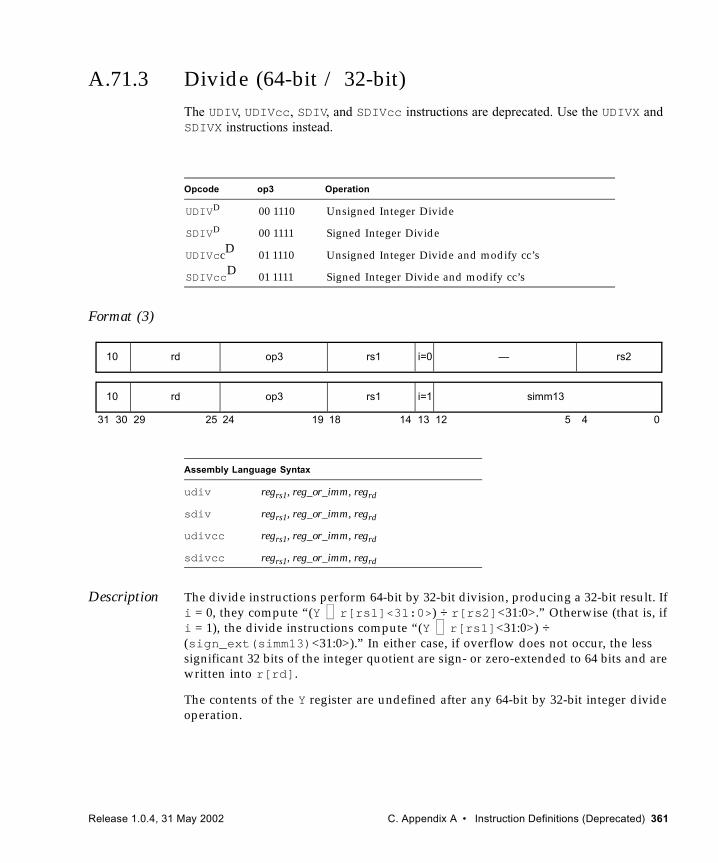
A.71.3 Divide (64-bit / 32-bit)The UDIV, UDIVcc, SDIV, and SDIVcc instructions are deprecated. Use the UDIVX and SDIVX instructions instead.
Format (3)
Description The divide instructions perform 64-bit by 32-bit division, producing a 32-bit result. If i = 0, they compute “(Y r[rs1]<31:0>) ÷ r[rs2]<31:0>.” Otherwise (that is, if i = 1), the divide instructions compute “(Y r[rs1]<31:0>) ÷ (sign_ext(simm13)<31:0>).” In either case, if overflow does not occur, the less significant 32 bits of the integer quotient are sign- or zero-extended to 64 bits and are written into r[rd].
The contents of the Y register are undefined after any 64-bit by 32-bit integer divide operation.
Opcode op3 Operation
UDIVD 00 1110 Unsigned Integer Divide
SDIVD 00 1111 Signed Integer Divide
UDIVccD 01 1110 Unsigned Integer Divide and modify cc’s
SDIVccD 01 1111 Signed Integer Divide and modify cc’s
Assembly Language Syntax
udiv regrs1, reg_or_imm, regrd
sdiv regrs1, reg_or_imm, regrd
udivcc regrs1, reg_or_imm, regrd
sdivcc regrs1, reg_or_imm, regrd
31 24 02530 29 19 18
rd10 op3 —
14 13 12 5 4
rs1 rs2i=0
rd10 op3 rs1 simm13i=1
Release 1.0.4, 31 May 2002 C. Appendix A • Instruction Definitions (Deprecated) 361
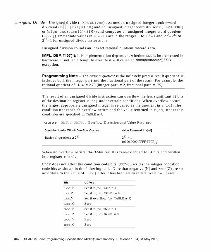
Unsigned Divide Unsigned divide (UDIV, UDIVcc) assumes an unsigned integer doubleword dividend (Y r[rs1]<31:0>) and an unsigned integer word divisor r[rs2<31:0>] or (sign_ext(simm13)<31:0>) and computes an unsigned integer word quotient (r[rd]). Immediate values in simm13 are in the ranges 0 to 212 – 1 and 232 – 212 to 232 – 1 for unsigned divide instructions.
Unsigned division rounds an inexact rational quotient toward zero.
IMPL. DEP. #107(1): It is implementation dependent whether LDD is implemented in hardware. If not, an attempt to execute it will cause an unimplemented_LDD exception.
Programming Note – The rational quotient is the infinitely precise result quotient. It includes both the integer part and the fractional part of the result. For example, the rational quotient of 11/4 = 2.75 (integer part = 2, fractional part = .75).
The result of an unsigned divide instruction can overflow the less significant 32 bits of the destination register r[rd] under certain conditions. When overflow occurs, the largest appropriate unsigned integer is returned as the quotient in r[rd]. The condition under which overflow occurs and the value returned in r[rd] under this condition are specified in TABLE A-9.
When no overflow occurs, the 32-bit result is zero-extended to 64 bits and written into register r[rd].
UDIV does not affect the condition code bits. UDIVcc writes the integer condition code bits as shown in the following table. Note that negative (N) and zero (Z) are set according to the value of r[rd] after it has been set to reflect overflow, if any.
TABLE A-9 UDIV / UDIVcc Overflow Detection and Value Returned
Condition Under Which Overflow Occurs Value Returned in r[rd]
Rational quotient ≥ 232 232 − 1(0000 0000 FFFF FFFF16)
Bit UDIVcc
icc.N Set if r[rd]<31> = 1
icc.Z Set if r[rd]<31:0> = 0
icc.V Set if overflow (per TABLE A-9)
icc.C Zero
xcc.N Set if r[rd]<63> = 1
xcc.Z Set if r[rd]<63:0> = 0
xcc.V Zero
xcc.C Zero
362 SPARC® Joint Programming Specification (JPS1): Commonality • Release 1.0.4, 31 May 2002
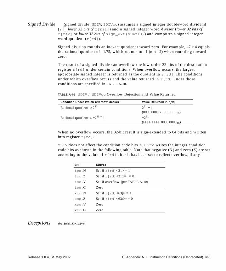
Signed Divide Signed divide (SDIV, SDIVcc) assumes a signed integer doubleword dividend (Y lower 32 bits of r[rs1]) and a signed integer word divisor (lower 32 bits of r[rs2] or lower 32 bits of sign_ext(simm13)) and computes a signed integer word quotient (r[rd]).
Signed division rounds an inexact quotient toward zero. For example, –7 ÷ 4 equals the rational quotient of –1.75, which rounds to –1 (not –2) when rounding toward zero.
The result of a signed divide can overflow the low-order 32 bits of the destination register r[rd] under certain conditions. When overflow occurs, the largest appropriate signed integer is returned as the quotient in r[rd]. The conditions under which overflow occurs and the value returned in r[rd] under those conditions are specified in TABLE A-10.
When no overflow occurs, the 32-bit result is sign-extended to 64 bits and written into register r[rd].
SDIV does not affect the condition code bits. SDIVcc writes the integer condition code bits as shown in the following table. Note that negative (N) and zero (Z) are set according to the value of r[rd] after it has been set to reflect overflow, if any.
Exceptions division_by_zero
TABLE A-10 SDIV / SDIVcc Overflow Detection and Value Returned
Condition Under Which Overflow Occurs Value Returned in r[rd]
Rational quotient ≥ 231 231 −1(0000 0000 7FFF FFFF16)
Rational quotient ≤ −231 − 1 −231
(FFFF FFFF 8000 000016)
Bit SDIVcc
icc.N Set if r[rd]<31> = 1
icc.Z Set if r[rd]<31:0> = 0
icc.V Set if overflow (per TABLE A-10)
icc.C Zero
xcc.N Set if r[rd]<63]> = 1
xcc.Z Set if r[rd]<63:0> = 0
xcc.V Zero
xcc.C Zero
Release 1.0.4, 31 May 2002 C. Appendix A • Instruction Definitions (Deprecated) 363
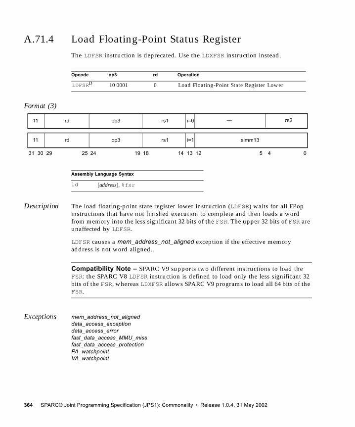
A.71.4 Load Floating-Point Status RegisterThe LDFSR instruction is deprecated. Use the LDXFSR instruction instead.
Format (3)
Description The load floating-point state register lower instruction (LDFSR) waits for all FPop instructions that have not finished execution to complete and then loads a word from memory into the less significant 32 bits of the FSR. The upper 32 bits of FSR are unaffected by LDFSR.
LDFSR causes a mem_address_not_aligned exception if the effective memory address is not word aligned.
Compatibility Note – SPARC V9 supports two different instructions to load the FSR: the SPARC V8 LDFSR instruction is defined to load only the less significant 32 bits of the FSR, whereas LDXFSR allows SPARC V9 programs to load all 64 bits of the FSR.
Exceptions mem_address_not_aligneddata_access_exceptiondata_access_errorfast_data_access_MMU_missfast_data_access_protectionPA_watchpointVA_watchpoint
Opcode op3 rd Operation
LDFSRD 10 0001 0 Load Floating-Point State Register Lower
Assembly Language Syntax
ld [address], %fsr
31 24 02530 29 19 18 14 13 12 5 4
rd11 op3 rs1 simm13i=1
rd11 op3 rs1 i=0 — rs2
364 SPARC® Joint Programming Specification (JPS1): Commonality • Release 1.0.4, 31 May 2002
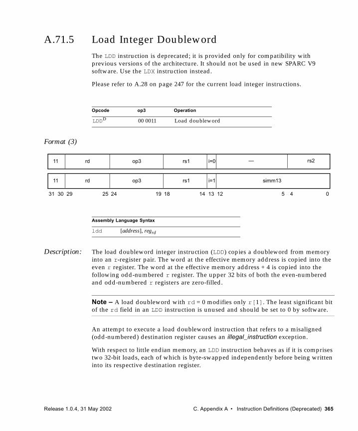
A.71.5 Load Integer DoublewordThe LDD instruction is deprecated; it is provided only for compatibility with previous versions of the architecture. It should not be used in new SPARC V9 software. Use the LDX instruction instead.
Please refer to A.28 on page 247 for the current load integer instructions.
Format (3)
Description: The load doubleword integer instruction (LDD) copies a doubleword from memory into an r-register pair. The word at the effective memory address is copied into the even r register. The word at the effective memory address + 4 is copied into the following odd-numbered r register. The upper 32 bits of both the even-numbered and odd-numbered r registers are zero-filled.
Note – A load doubleword with rd = 0 modifies only r[1]. The least significant bit of the rd field in an LDD instruction is unused and should be set to 0 by software.
An attempt to execute a load doubleword instruction that refers to a misaligned (odd-numbered) destination register causes an illegal_instruction exception.
With respect to little endian memory, an LDD instruction behaves as if it is comprises two 32-bit loads, each of which is byte-swapped independently before being written into its respective destination register.
Opcode op3 Operation
LDDD 00 0011 Load doubleword
Assembly Language Syntax
ldd [address], regrd
31 24 02530 29 19 18 14 13 12 5 4
rd11 op3 rs1 simm13i=1
rd11 op3 rs1 i=0 — rs2
Release 1.0.4, 31 May 2002 C. Appendix A • Instruction Definitions (Deprecated) 365
Load integer doubleword instructions access the primary address space (ASI = 8016). The effective address is “r[rs1] + r[rs2]” if i = 0, or “r[rs1] + sign_ext(simm13)” if i = 1.
A successful load doubleword instruction operates atomically.
Programming Note – LDD is provided for compatibility with SPARC V8. It may execute slowly on SPARC V9 machines because of data path and register-access difficulties.
Exceptions illegal_instruction (LDD with odd rd)mem_address_not_aligneddata_access_exceptiondata_access_errorfast_data_access_MMU_missfast_data_access_protectionPA_watchpointVA_watchpoint
366 SPARC® Joint Programming Specification (JPS1): Commonality • Release 1.0.4, 31 May 2002
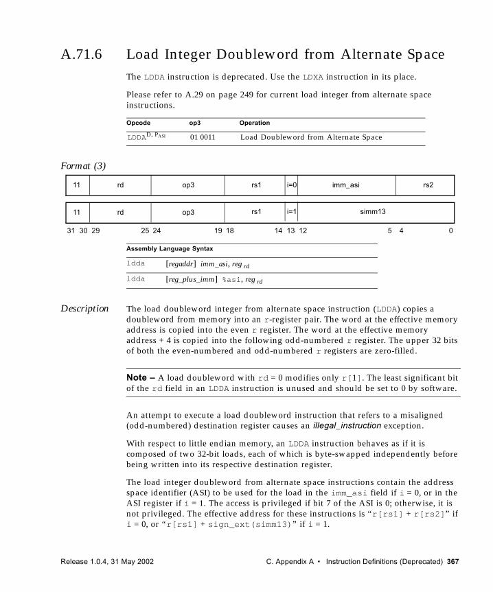
A.71.6 Load Integer Doubleword from Alternate SpaceThe LDDA instruction is deprecated. Use the LDXA instruction in its place.
Please refer to A.29 on page 249 for current load integer from alternate space instructions.
Format (3)
Description The load doubleword integer from alternate space instruction (LDDA) copies a doubleword from memory into an r-register pair. The word at the effective memory address is copied into the even r register. The word at the effective memory address + 4 is copied into the following odd-numbered r register. The upper 32 bits of both the even-numbered and odd-numbered r registers are zero-filled.
Note – A load doubleword with rd = 0 modifies only r[1]. The least significant bit of the rd field in an LDDA instruction is unused and should be set to 0 by software.
An attempt to execute a load doubleword instruction that refers to a misaligned (odd-numbered) destination register causes an illegal_instruction exception.
With respect to little endian memory, an LDDA instruction behaves as if it is composed of two 32-bit loads, each of which is byte-swapped independently before being written into its respective destination register.
The load integer doubleword from alternate space instructions contain the address space identifier (ASI) to be used for the load in the imm_asi field if i = 0, or in the ASI register if i = 1. The access is privileged if bit 7 of the ASI is 0; otherwise, it is not privileged. The effective address for these instructions is “r[rs1] + r[rs2]” if i = 0, or “r[rs1] + sign_ext(simm13)” if i = 1.
Opcode op3 Operation
LDDAD, PASI 01 0011 Load Doubleword from Alternate Space
Assembly Language Syntax
ldda [regaddr] imm_asi, reg rd
ldda [reg_plus_imm] %asi, reg rd
31 24 02530 29 19 18
rd11 op3 imm_asi
14 13 12 5 4
rs1 rs2i=0
rd11 op3 rs1 i=1 simm13
Release 1.0.4, 31 May 2002 C. Appendix A • Instruction Definitions (Deprecated) 367
A successful load doubleword instruction operates atomically.
LDDA causes a mem_address_not_aligned exception if the address is not doubleword aligned.
These instructions cause a privileged_action exception if PSTATE.PRIV = 0 and bit 7 of the ASI is 0.
LDDA with ASI = 2416 or 2C16 is defined to be a Load Quadword Atomic instruction. See A.30 on page 251 for details.
LDDA with ASI = 7016, 7116, 7816, 7916, F016, F116, F816, or F916 is defined to be a Block Load instruction. See A.4 on page 199 for details.
LDDA with ASI = D016–D316 or D816–DB16 is defined to be a Short Floating-point Load instruction. See A.58 on page 326 for details.
IMPL. DEP. #107(2): It is implementation dependent whether LDDA is implemented in hardware. If not, an attempt to execute it will cause an unimplemented_LDD exception.
Programming Note – LDDA is provided for compatibility with SPARC V8. It may execute slowly on SPARC V9 machines because of data path and register-access difficulties.
If LDDA is emulated in software, an LDXA instruction should be used for the memory access in order to preserve atomicity.
Exceptions privileged_actionillegal_instruction (LDDA with odd rd)mem_address_not_aligned)data_access_exceptionfast_data_access_MMU_missfast_data_access_protectionPA_watchpointVA_watchpoint
368 SPARC® Joint Programming Specification (JPS1): Commonality • Release 1.0.4, 31 May 2002
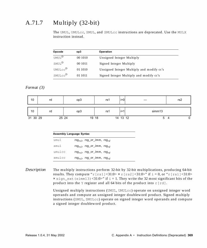
A.71.7 Multiply (32-bit)The UMUL, UMULcc, SMUL, and SMULcc instructions are deprecated. Use the MULX instruction instead.
Format (3)
Description The multiply instructions perform 32-bit by 32-bit multiplications, producing 64-bit results. They compute “r[rs1]<31:0> × r[rs2]<31:0>” if i = 0, or “r[rs1]<31:0> × sign_ext(simm13)<31:0>” if i = 1. They write the 32 most significant bits of the product into the Y register and all 64 bits of the product into r[rd].
Unsigned multiply instructions (UMUL, UMULcc) operate on unsigned integer word operands and compute an unsigned integer doubleword product. Signed multiply instructions (SMUL, SMULcc) operate on signed integer word operands and compute a signed integer doubleword product.
Opcode op3 Operation
UMULD 00 1010 Unsigned Integer Multiply
SMULD 00 1011 Signed Integer Multiply
UMULccD 01 1010 Unsigned Integer Multiply and modify cc’s
SMULccD 01 1011 Signed Integer Multiply and modify cc’s
Assembly Language Syntax
umul regrs1, reg_or_imm, regrd
smul regrs1, reg_or_imm, regrd
umulcc regrs1, reg_or_imm, regrd
smulcc regrs1, reg_or_imm, regrd
31 24 02530 29 19 18
rd10 op3 —
14 13 12 5 4
rs1 rs2i=0
rd10 op3 rs1 simm13i=1
Release 1.0.4, 31 May 2002 C. Appendix A • Instruction Definitions (Deprecated) 369
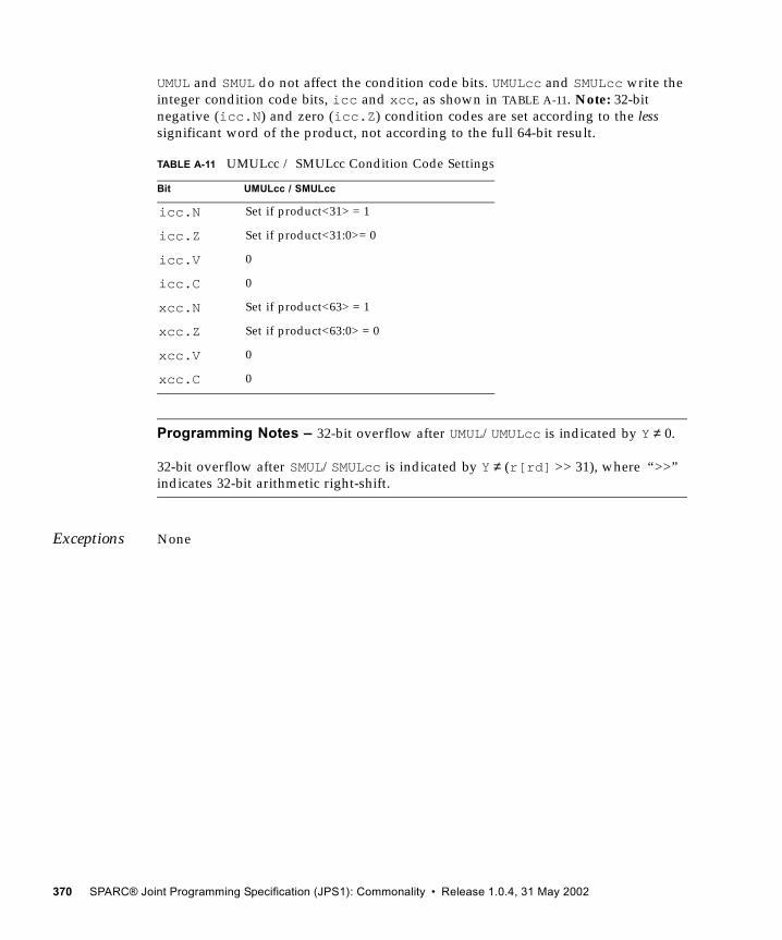
UMUL and SMUL do not affect the condition code bits. UMULcc and SMULcc write the integer condition code bits, icc and xcc, as shown in TABLE A-11. Note: 32-bit negative (icc.N) and zero (icc.Z) condition codes are set according to the less significant word of the product, not according to the full 64-bit result.
Programming Notes – 32-bit overflow after UMUL/UMULcc is indicated by Y ≠ 0.
32-bit overflow after SMUL/SMULcc is indicated by Y ≠ (r[rd] >> 31), where “>>” indicates 32-bit arithmetic right-shift.
Exceptions None
TABLE A-11 UMULcc / SMULcc Condition Code Settings
Bit UMULcc / SMULcc
icc.N Set if product<31> = 1
icc.Z Set if product<31:0>= 0
icc.V 0
icc.C 0
xcc.N Set if product<63> = 1
xcc.Z Set if product<63:0> = 0
xcc.V 0
xcc.C 0
370 SPARC® Joint Programming Specification (JPS1): Commonality • Release 1.0.4, 31 May 2002
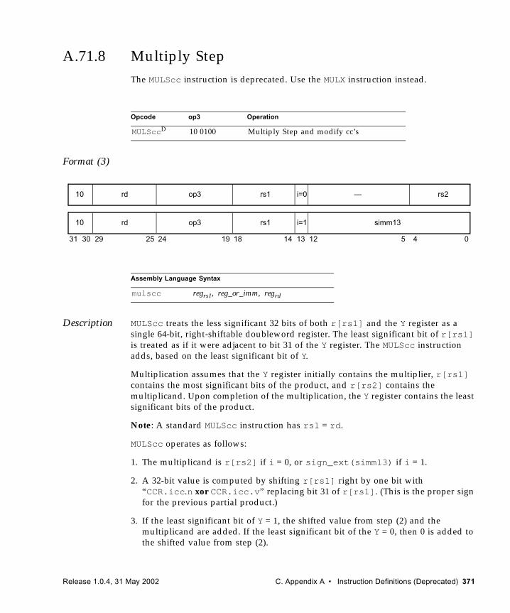
A.71.8 Multiply StepThe MULScc instruction is deprecated. Use the MULX instruction instead.
Format (3)
Description MULScc treats the less significant 32 bits of both r[rs1] and the Y register as a single 64-bit, right-shiftable doubleword register. The least significant bit of r[rs1] is treated as if it were adjacent to bit 31 of the Y register. The MULScc instruction adds, based on the least significant bit of Y.
Multiplication assumes that the Y register initially contains the multiplier, r[rs1] contains the most significant bits of the product, and r[rs2] contains the multiplicand. Upon completion of the multiplication, the Y register contains the least significant bits of the product.
Note: A standard MULScc instruction has rs1 = rd.
MULScc operates as follows:
1. The multiplicand is r[rs2] if i = 0, or sign_ext(simm13) if i = 1.
2. A 32-bit value is computed by shifting r[rs1] right by one bit with “CCR.icc.n xor CCR.icc.v” replacing bit 31 of r[rs1]. (This is the proper sign for the previous partial product.)
3. If the least significant bit of Y = 1, the shifted value from step (2) and the multiplicand are added. If the least significant bit of the Y = 0, then 0 is added to the shifted value from step (2).
Opcode op3 Operation
MULSccD 10 0100 Multiply Step and modify cc’s
Assembly Language Syntax
mulscc regrs1, reg_or_imm, regrd
31 24 02530 29 19 18
rd10 op3 —
14 13 12 5 4
rs1 rs2i=0
rd10 op3 rs1 simm13i=1
Release 1.0.4, 31 May 2002 C. Appendix A • Instruction Definitions (Deprecated) 371
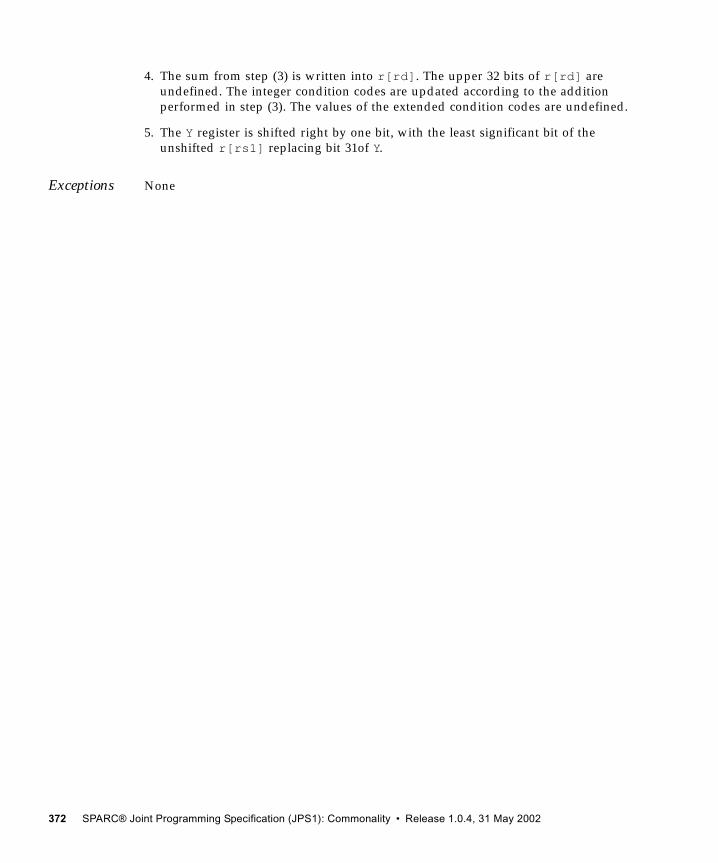
4. The sum from step (3) is written into r[rd]. The upper 32 bits of r[rd] are undefined. The integer condition codes are updated according to the addition performed in step (3). The values of the extended condition codes are undefined.
5. The Y register is shifted right by one bit, with the least significant bit of the unshifted r[rs1] replacing bit 31of Y.
Exceptions None
372 SPARC® Joint Programming Specification (JPS1): Commonality • Release 1.0.4, 31 May 2002
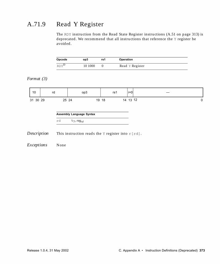
A.71.9 Read Y RegisterThe RDY instruction from the Read State Register instructions (A.51 on page 313) is deprecated. We recommend that all instructions that reference the Y register be avoided.
Format (3)
Description This instruction reads the Y register into r[rd].
Exceptions None
Opcode op3 rs1 Operation
RDYD 10 1000 0 Read Y Register
Assembly Language Syntax
rd %y, regrd
31 141924 18 13 02530 29
10 rd op3 rs1 —
12
i=0
Release 1.0.4, 31 May 2002 C. Appendix A • Instruction Definitions (Deprecated) 373
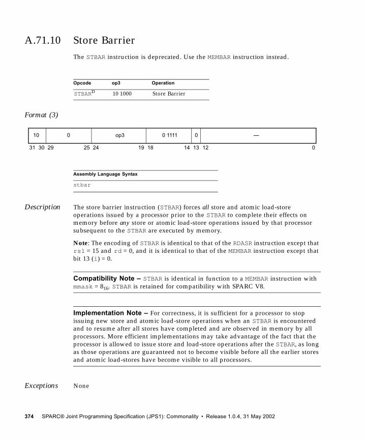
A.71.10 Store BarrierThe STBAR instruction is deprecated. Use the MEMBAR instruction instead.
Format (3)
Description The store barrier instruction (STBAR) forces all store and atomic load-store operations issued by a processor prior to the STBAR to complete their effects on memory before any store or atomic load-store operations issued by that processor subsequent to the STBAR are executed by memory.
Note: The encoding of STBAR is identical to that of the RDASR instruction except that rs1 = 15 and rd = 0, and it is identical to that of the MEMBAR instruction except that bit 13 (i) = 0.
Compatibility Note – STBAR is identical in function to a MEMBAR instruction with mmask = 816. STBAR is retained for compatibility with SPARC V8.
Implementation Note – For correctness, it is sufficient for a processor to stop issuing new store and atomic load-store operations when an STBAR is encountered and to resume after all stores have completed and are observed in memory by all processors. More efficient implementations may take advantage of the fact that the processor is allowed to issue store and load-store operations after the STBAR, as long as those operations are guaranteed not to become visible before all the earlier stores and atomic load-stores have become visible to all processors.
Exceptions None
Opcode op3 Operation
STBARD 10 1000 Store Barrier
Assembly Language Syntax
stbar
31 141924 18 13 02530 29
10 0 op3 0 1111 —
12
0
374 SPARC® Joint Programming Specification (JPS1): Commonality • Release 1.0.4, 31 May 2002
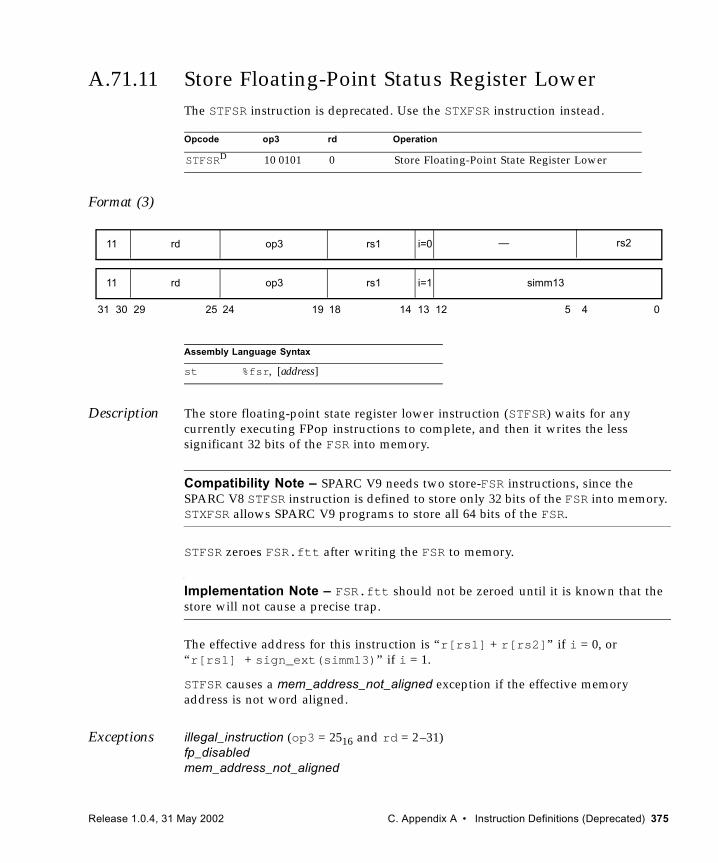
A.71.11 Store Floating-Point Status Register LowerThe STFSR instruction is deprecated. Use the STXFSR instruction instead.
Format (3)
Description The store floating-point state register lower instruction (STFSR) waits for any currently executing FPop instructions to complete, and then it writes the less significant 32 bits of the FSR into memory.
Compatibility Note – SPARC V9 needs two store-FSR instructions, since the SPARC V8 STFSR instruction is defined to store only 32 bits of the FSR into memory. STXFSR allows SPARC V9 programs to store all 64 bits of the FSR.
STFSR zeroes FSR.ftt after writing the FSR to memory.
Implementation Note – FSR.ftt should not be zeroed until it is known that the store will not cause a precise trap.
The effective address for this instruction is “r[rs1] + r[rs2]” if i = 0, or “r[rs1] + sign_ext(simm13)” if i = 1.
STFSR causes a mem_address_not_aligned exception if the effective memory address is not word aligned.
Exceptions illegal_instruction (op3 = 2516 and rd = 2–31)fp_disabled mem_address_not_aligned
Opcode op3 rd Operation
STFSRD 10 0101 0 Store Floating-Point State Register Lower
Assembly Language Syntax
st %fsr, [address]
31 24 02530 29 19 18 14 13 12 5 4
rd11 op3 rs1 simm13i=1
rd11 op3 rs1 i=0 — rs2
Release 1.0.4, 31 May 2002 C. Appendix A • Instruction Definitions (Deprecated) 375
data_access_exceptiondata_access_errorfast_data_access_MMU_missfast_data_access_protectionPA_watchpointVA_watchpoint
376 SPARC® Joint Programming Specification (JPS1): Commonality • Release 1.0.4, 31 May 2002
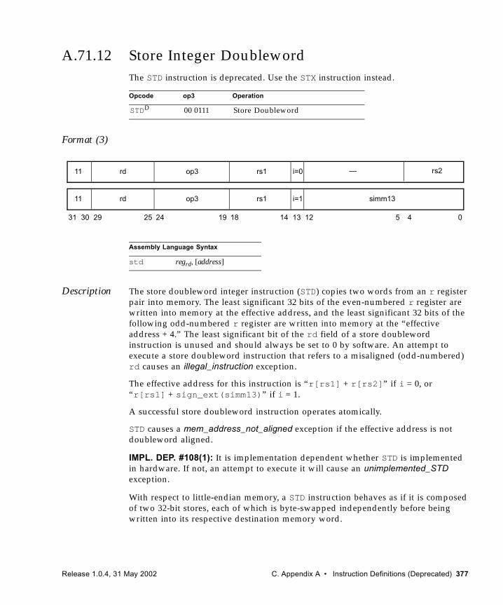
A.71.12 Store Integer DoublewordThe STD instruction is deprecated. Use the STX instruction instead.
Format (3)
Description The store doubleword integer instruction (STD) copies two words from an r register pair into memory. The least significant 32 bits of the even-numbered r register are written into memory at the effective address, and the least significant 32 bits of the following odd-numbered r register are written into memory at the “effective address + 4.” The least significant bit of the rd field of a store doubleword instruction is unused and should always be set to 0 by software. An attempt to execute a store doubleword instruction that refers to a misaligned (odd-numbered) rd causes an illegal_instruction exception.
The effective address for this instruction is “r[rs1] + r[rs2]” if i = 0, or “r[rs1] + sign_ext(simm13)” if i = 1.
A successful store doubleword instruction operates atomically.
STD causes a mem_address_not_aligned exception if the effective address is not doubleword aligned.
IMPL. DEP. #108(1): It is implementation dependent whether STD is implemented in hardware. If not, an attempt to execute it will cause an unimplemented_STD exception.
With respect to little-endian memory, a STD instruction behaves as if it is composed of two 32-bit stores, each of which is byte-swapped independently before being written into its respective destination memory word.
Opcode op3 Operation
STDD 00 0111 Store Doubleword
Assembly Language Syntax
std regrd, [address]
31 24 02530 29 19 18 14 13 12 5 4
rd11 op3 rs1 simm13i=1
rd11 op3 rs1 i=0 — rs2
Release 1.0.4, 31 May 2002 C. Appendix A • Instruction Definitions (Deprecated) 377
Programming Notes – STD is provided for compatibility with SPARC V8. It may execute slowly on SPARC V9 machines because of data path and register-access difficulties. Therefore, software should avoid using STD.
If STD is emulated in software, STX should be used to preserve atomicity.
Exceptions illegal_instruction (STD with odd rd)mem_address_not_aligned (all except STB)data_access_exceptiondata_access_errorfast_data_access_MMU_missfast_data_access_protectionPA_watchpointVA_watchpoint
378 SPARC® Joint Programming Specification (JPS1): Commonality • Release 1.0.4, 31 May 2002
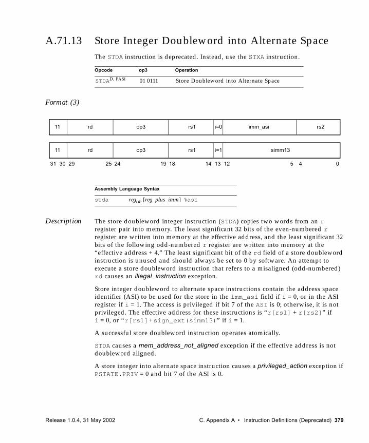
A.71.13 Store Integer Doubleword into Alternate SpaceThe STDA instruction is deprecated. Instead, use the STXA instruction.
Format (3)
Description The store doubleword integer instruction (STDA) copies two words from an r register pair into memory. The least significant 32 bits of the even-numbered r register are written into memory at the effective address, and the least significant 32 bits of the following odd-numbered r register are written into memory at the “effective address + 4.” The least significant bit of the rd field of a store doubleword instruction is unused and should always be set to 0 by software. An attempt to execute a store doubleword instruction that refers to a misaligned (odd-numbered) rd causes an illegal_instruction exception.
Store integer doubleword to alternate space instructions contain the address space identifier (ASI) to be used for the store in the imm_asi field if i = 0, or in the ASI register if i = 1. The access is privileged if bit 7 of the ASI is 0; otherwise, it is not privileged. The effective address for these instructions is “r[rs1] + r[rs2]” if i = 0, or “r[rs1]+sign_ext(simm13)” if i = 1.
A successful store doubleword instruction operates atomically.
STDA causes a mem_address_not_aligned exception if the effective address is not doubleword aligned.
A store integer into alternate space instruction causes a privileged_action exception if PSTATE.PRIV = 0 and bit 7 of the ASI is 0.
Opcode op3 Operation
STDAD, PASI 01 0111 Store Doubleword into Alternate Space
Assembly Language Syntax
stda regrd, [reg_plus_imm] %asi
31 24 02530 29 19 18
rd11 op3 imm_asi
14 13 12 5 4
rs1 rs2i=0
rd11 op3 rs1 simm13i=1
Release 1.0.4, 31 May 2002 C. Appendix A • Instruction Definitions (Deprecated) 379
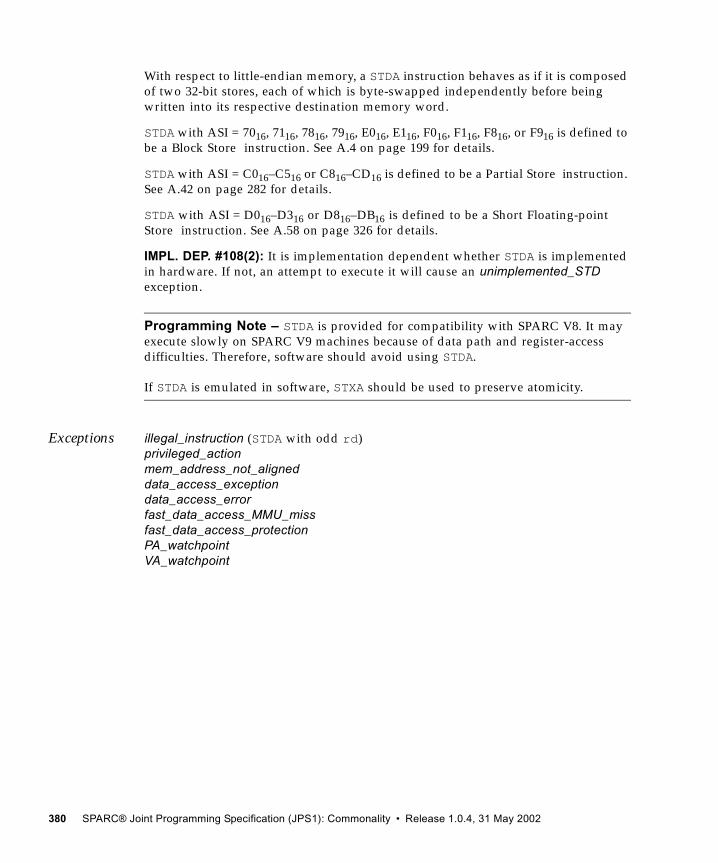
With respect to little-endian memory, a STDA instruction behaves as if it is composed of two 32-bit stores, each of which is byte-swapped independently before being written into its respective destination memory word.
STDA with ASI = 7016, 7116, 7816, 7916, E016, E116, F016, F116, F816, or F916 is defined to be a Block Store instruction. See A.4 on page 199 for details.
STDA with ASI = C016–C516 or C816–CD16 is defined to be a Partial Store instruction. See A.42 on page 282 for details.
STDA with ASI = D016–D316 or D816–DB16 is defined to be a Short Floating-point Store instruction. See A.58 on page 326 for details.
IMPL. DEP. #108(2): It is implementation dependent whether STDA is implemented in hardware. If not, an attempt to execute it will cause an unimplemented_STD exception.
Programming Note – STDA is provided for compatibility with SPARC V8. It may execute slowly on SPARC V9 machines because of data path and register-access difficulties. Therefore, software should avoid using STDA.
If STDA is emulated in software, STXA should be used to preserve atomicity.
Exceptions illegal_instruction (STDA with odd rd)privileged_action mem_address_not_aligneddata_access_exceptiondata_access_errorfast_data_access_MMU_missfast_data_access_protectionPA_watchpointVA_watchpoint
380 SPARC® Joint Programming Specification (JPS1): Commonality • Release 1.0.4, 31 May 2002
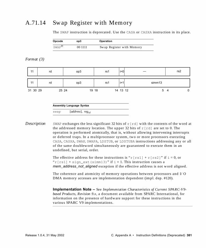
A.71.14 Swap Register with MemoryThe SWAP instruction is deprecated. Use the CASA or CASXA instruction in its place.
Format (3)
Description SWAP exchanges the less significant 32 bits of r[rd] with the contents of the word at the addressed memory location. The upper 32 bits of r[rd] are set to 0. The operation is performed atomically, that is, without allowing intervening interrupts or deferred traps. In a multiprocessor system, two or more processors executing CASA, CASXA, SWAP, SWAPA, LDSTUB, or LDSTUBA instructions addressing any or all of the same doubleword simultaneously are guaranteed to execute them in an undefined, but serial, order.
The effective address for these instructions is “r[rs1] + r[rs2]” if i = 0, or “r[rs1] + sign_ext(simm13)” if i = 1. This instruction causes a mem_address_not_aligned exception if the effective address is not word aligned.
The coherence and atomicity of memory operations between processors and I/O DMA memory accesses are implementation dependent (impl. dep. #120).
Implementation Note – See Implementation Characteristics of Current SPARC-V9-based Products, Revision 9.x, a document available from SPARC International, for information on the presence of hardware support for these instructions in the various SPARC V9 implementations.
Opcode op3 Operation
SWAPD 00 1111 Swap Register with Memory
Assembly Language Syntax
swap [address], regrd
31 24 02530 29 19 18 14 13 12 5 4
rd11 op3 rs1 simm13i=1
rd11 op3 rs1 i=0 — rs2
Release 1.0.4, 31 May 2002 C. Appendix A • Instruction Definitions (Deprecated) 381
Exceptions mem_address_not_aligned data_access_exceptiondata_access_errorfast_data_access_MMU_missfast_data_access_protectionPA_watchpointVA_watchpoint
382 SPARC® Joint Programming Specification (JPS1): Commonality • Release 1.0.4, 31 May 2002
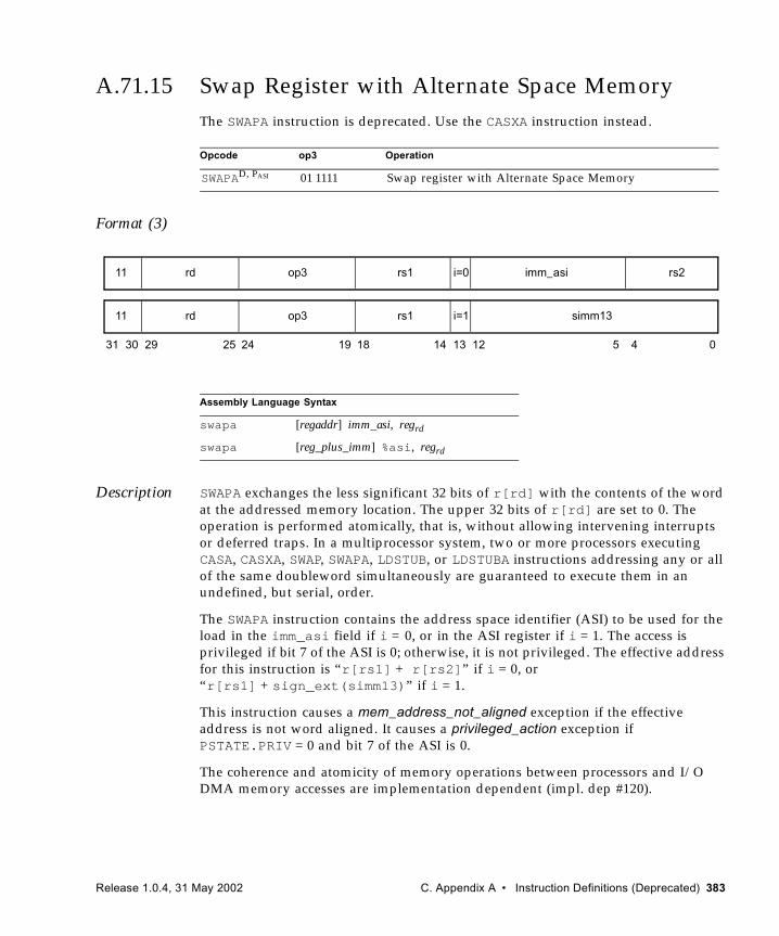
A.71.15 Swap Register with Alternate Space MemoryThe SWAPA instruction is deprecated. Use the CASXA instruction instead.
Format (3)
Description SWAPA exchanges the less significant 32 bits of r[rd] with the contents of the word at the addressed memory location. The upper 32 bits of r[rd] are set to 0. The operation is performed atomically, that is, without allowing intervening interrupts or deferred traps. In a multiprocessor system, two or more processors executing CASA, CASXA, SWAP, SWAPA, LDSTUB, or LDSTUBA instructions addressing any or all of the same doubleword simultaneously are guaranteed to execute them in an undefined, but serial, order.
The SWAPA instruction contains the address space identifier (ASI) to be used for the load in the imm_asi field if i = 0, or in the ASI register if i = 1. The access is privileged if bit 7 of the ASI is 0; otherwise, it is not privileged. The effective address for this instruction is “r[rs1] + r[rs2]” if i = 0, or “r[rs1] + sign_ext(simm13)” if i = 1.
This instruction causes a mem_address_not_aligned exception if the effective address is not word aligned. It causes a privileged_action exception if PSTATE.PRIV = 0 and bit 7 of the ASI is 0.
The coherence and atomicity of memory operations between processors and I/O DMA memory accesses are implementation dependent (impl. dep #120).
Opcode op3 Operation
SWAPAD, PASI 01 1111 Swap register with Alternate Space Memory
Assembly Language Syntax
swapa [regaddr] imm_asi, regrd
swapa [reg_plus_imm] %asi, regrd
31 24 02530 29 19 18
rd11 op3 imm_asi
14 13 12 5 4
rs1 rs2i=0
rd11 op3 rs1 simm13i=1
Release 1.0.4, 31 May 2002 C. Appendix A • Instruction Definitions (Deprecated) 383
Implementation Note – See Implementation Characteristics of Current SPARC-V9-based Products, Revision 9.x, a document available from SPARC International, for information on the presence of hardware support for this instruction in the various SPARC V9 implementations.
Exceptions mem_address_not_aligned privileged_action data_access_exceptiondata_access_errorfast_data_access_MMU_missfast_data_access_protectionPA_watchpointVA_watchpoint
384 SPARC® Joint Programming Specification (JPS1): Commonality • Release 1.0.4, 31 May 2002
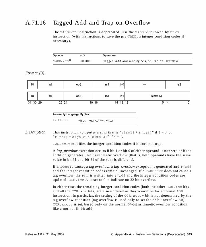
A.71.16 Tagged Add and Trap on OverflowThe TADDccTV instruction is deprecated. Use the TADDcc followed by BPVS instruction (with instructions to save the pre-TADDcc integer condition codes if necessary).
Format (3)
Description This instruction computes a sum that is “r[rs1] + r[rs2]” if i = 0, or “r[rs1] + sign_ext(simm13)” if i = 1.
TADDccTV modifies the integer condition codes if it does not trap.
A tag_overflow exception occurs if bit 1 or bit 0 of either operand is nonzero or if the addition generates 32-bit arithmetic overflow (that is, both operands have the same value in bit 31 and bit 31 of the sum is different).
If TADDccTV causes a tag overflow, a tag_overflow exception is generated and r[rd] and the integer condition codes remain unchanged. If a TADDccTV does not cause a tag overflow, the sum is written into r[rd] and the integer condition codes are updated. CCR.icc.v is set to 0 to indicate no 32-bit overflow.
In either case, the remaining integer condition codes (both the other CCR.icc bits and all the CCR.xcc bits) are also updated as they would be for a normal ADD instruction. In particular, the setting of the CCR.xcc.v bit is not determined by the tag overflow condition (tag overflow is used only to set the 32-bit overflow bit). CCR.xcc.v is set, based only on the normal 64-bit arithmetic overflow condition, like a normal 64-bit add.
Opcode op3 Operation
TADDccTVD 10 0010 Tagged Add and modify cc’s, or Trap on Overflow
Assembly Language Syntax
taddcctv regrs1, reg_or_imm, regrd
31 24 02530 29 19 18
rd10 op3 —
14 13 12 5 4
rs1 rs2i=0
rd10 op3 rs1 simm13i=1
Release 1.0.4, 31 May 2002 C. Appendix A • Instruction Definitions (Deprecated) 385
Compatibility Note – TADDccTV traps based on the 32-bit overflow condition, just as in SPARC V8. Although the tagged add instructions set the 64-bit condition codes CCR.xcc, there is no form of the instruction that traps the 64-bit overflow condition.
Exceptions tag_overflow
386 SPARC® Joint Programming Specification (JPS1): Commonality • Release 1.0.4, 31 May 2002
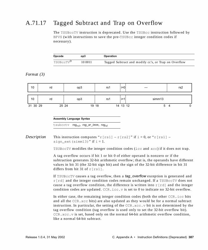
A.71.17 Tagged Subtract and Trap on OverflowThe TSUBccTV instruction is deprecated. Use the TSUBcc instruction followed by BPVS (with instructions to save the pre-TSUBcc integer condition codes if necessary).
Format (3)
Description This instruction computes “r[rs1] – r[rs2]” if i = 0, or “r[rs1] – sign_ext(simm13)” if i = 1.
TSUBccTV modifies the integer condition codes (icc and xcc) if it does not trap.
A tag overflow occurs if bit 1 or bit 0 of either operand is nonzero or if the subtraction generates 32-bit arithmetic overflow; that is, the operands have different values in bit 31 (the 32-bit sign bit) and the sign of the 32-bit difference in bit 31 differs from bit 31 of r[rs1].
If TSUBccTV causes a tag overflow, then a tag_overflow exception is generated and r[rd] and the integer condition codes remain unchanged. If a TSUBccTV does not cause a tag overflow condition, the difference is written into r[rd] and the integer condition codes are updated. CCR.icc.v is set to 0 to indicate no 32-bit overflow.
In either case, the remaining integer condition codes (both the other CCR.icc bits and all the CCR.xcc bits) are also updated as they would be for a normal subtract instruction. In particular, the setting of the CCR.xcc.v bit is not determined by the tag overflow condition (tag overflow is used only to set the 32-bit overflow bit). CCR.xcc.v is set, based only on the normal 64-bit arithmetic overflow condition, like a normal 64-bit subtract.
Opcode op3 Operation
TSUBccTVD 10 0011 Tagged Subtract and modify cc’s, or Trap on Overflow
Assembly Language Syntax
tsubcctv regrs1, reg_or_imm, regrd
31 24 02530 29 19 18
rd10 op3 —
14 13 12 5 4
rs1 rs2i=0
rd10 op3 rs1 simm13i=1
Release 1.0.4, 31 May 2002 C. Appendix A • Instruction Definitions (Deprecated) 387
Compatibility Note – TSUBccTV traps are based on the 32-bit overflow condition, just as in SPARC V8. Although the tagged-subtract instructions set the 64-bit condition codes CCR.xcc, there is no form of the instruction that traps on 64-bit overflow.
Exceptions tag_overflow
388 SPARC® Joint Programming Specification (JPS1): Commonality • Release 1.0.4, 31 May 2002
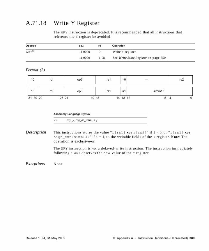
A.71.18 Write Y RegisterThe WRY instruction is deprecated. It is recommended that all instructions that reference the Y register be avoided.
Format (3)
Description This instructions stores the value “r[rs1] xor r[rs2]” if i = 0, or “r[rs1] xor sign_ext(simm13)” if i = 1, to the writable fields of the Y register. Note: The operation is exclusive-or.
The WRY instruction is not a delayed-write instruction. The instruction immediately following a WRY observes the new value of the Y register.
Exceptions None
Opcode op3 rd Operation
WRYD 11 0000 0 Write Y register
— 11 0000 1–31 See Write State Register on page 350
Assembly Language Syntax
wr regrs1, reg_or_imm, %y
31 24 02530 29 19 18
rd10 op3 —
14 13 12 5 4
rs1 rs2i=0
rd10 op3 rs1 simm13i=1
Release 1.0.4, 31 May 2002 C. Appendix A • Instruction Definitions (Deprecated) 389

390 SPARC® Joint Programming Specification (JPS1): Commonality • Release 1.0.4, 31 May 2002
C.APPENDIX B
IEEE Std 754-1985 Requirements for SPARC V9
The IEEE Std 754-1985 floating-point standard contains a number of implementation dependencies. This appendix specifies choices for these implementation dependencies, to ensure that SPARC V9 implementations are as consistent as possible.
The appendix contains these major sections:
■ Traps Inhibiting Results on page 392■ NaN Operand and Result Definitions on page 392■ Trapped Underflow Definition (UFM = 1) on page 394■ Untrapped Underflow Definition (UFM = 0) on page 395■ Integer Overflow Definition on page 396■ Floating-Point Nonstandard Mode on page 396
Exceptions are discussed in this appendix on the assumption that instructions are implemented in hardware. If an instruction is implemented in software, it may not trigger hardware exceptions but its behavior as observed by nonprivileged software (other than timing) must be the same as if it was implemented in hardware.
Release 1.0.4, 31 May 2002 C. Appendix B • IEEE Std 754-1985 Requirements for SPARC V9 391
B.1 Traps Inhibiting ResultsAs described in Floating-Point State Register (FSR) on page 56 and elsewhere, when a floating-point trap occurs, the following conditions are true:
■ The destination floating-point register(s) (the f registers) are unchanged.
■ The floating-point condition codes (fcc0, fcc1, fcc2, and fcc3) are unchanged.
■ The FSR.aexc (accrued exceptions) field is unchanged.
■ The FSR.cexc (current exceptions) field is unchanged except for IEEE_754_exceptions; in that case, cexc contains a bit set to 1, corresponding to the exception that caused the trap. Only one bit shall be set in cexc.
Instructions causing an fp_exception_other trap because of unfinished or unimplemented FPops execute as if by hardware; that is, a trap is undetectable by user software, except that timing may be affected. A user-mode trap handler invoked for an IEEE_754_exception, whether as a direct result of a hardware fp_exception_ieee_754 trap or as an indirect result of supervisor handling of an fp_exception_other trap with FSR.ftt = unfinished_FPop or FSR.ftt = unimplemented_FPop, can rely on the following behavior:
■ The address of the instruction that caused the exception will be available.
■ The destination floating-point register(s) are unchanged from their state prior to that instruction’s execution.
■ The floating-point condition codes (fcc0, fcc1, fcc2, and fcc3) are unchanged.
■ The FSR aexc field is unchanged.
■ The FSR cexc field contains exactly one bit set to 1, corresponding to the exception that caused the trap.
■ The FSR ftt, qne, and reserved fields are zero.
B.2 NaN Operand and Result DefinitionsAn untrapped floating-point result can be in a format that is either the same as, or different from, the format of the source operands. These two cases are described separately below.
392 SPARC® Joint Programming Specification (JPS1): Commonality • Release 1.0.4, 31 May 2002
B.2.1 Untrapped Result in Different Format from Operands■ F[sdq]TO[sdq] with a quiet NaN operand — No exception caused; result is a
quiet NaN. The operand is transformed as follows:
NaN transformation: The most significant bits of the operand fraction are copied to the most significant bits of the result fraction. In conversion to a narrower format, excess low-order bits of the operand fraction are discarded. In conversion to a wider format, excess low-order bits of the result fraction are set to 0. The quiet bit (the most significant bit of the result fraction) is always set to 1, so the NaN transformation always produces a quiet NaN. The sign bit is copied from the operand to the result without modification.
■ F[sdq]TO[sdq] with a signalling NaN operand — Invalid exception; result is the signalling NaN operand processed by the NaN transformation above to produce a quiet NaN.
■ FCMPE[sdq] with any NaN operand — Invalid exception; the selected floating-point condition code is set to unordered.
■ FCMP[sdq] with any signalling NaN operand — Invalid exception; the selected floating-point condition code is set to unordered.
■ FCMP[sdq] with any quiet NaN operand but no signalling NaN operand — No exception; the selected floating-point condition code is set to unordered.
B.2.2 Untrapped Result in Same Format as Operands■ No NaN operand — For an invalid operation such as sqrt(–1.0) or 0.0 ÷ 0.0, the
result is the quiet NaN with sign = zero, exponent = all ones, and fraction = all ones. The sign is zero to distinguish such results from storage initialized to all ones.
■ One operand, a quiet NaN — No exception; result is the quiet NaN operand.
■ One operand, a signalling NaN — Invalid exception; result is the signalling NaN with its quiet bit (most significant bit of fraction field) set to 1.
■ Two operands, both quiet NaNs — No exception; result is the rs2 (second source) operand.
■ Two operands, both signalling NaNs — Invalid exception; result is the rs2 operand with the quiet bit set to 1.
■ Two operands, only one is a signalling NaN — Invalid exception; result is the signalling NaN operand with the quiet bit set to 1.
■ Two operands, neither is a signalling NaN, only one is a quiet NaN — No exception; result is the quiet NaN operand.
Release 1.0.4, 31 May 2002 C. Appendix B • IEEE Std 754-1985 Requirements for SPARC V9 393
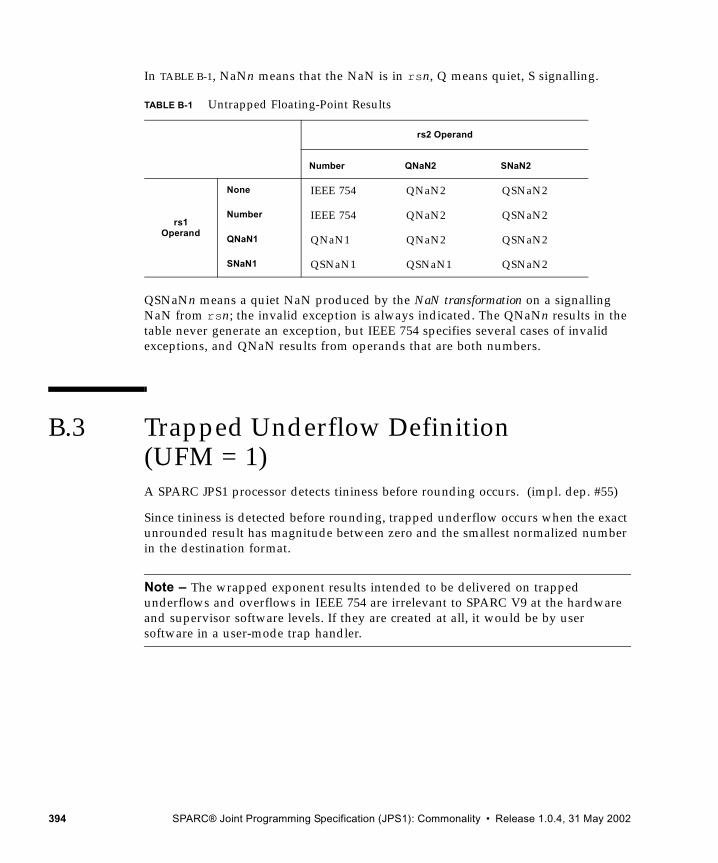
In TABLE B-1, NaNn means that the NaN is in rsn, Q means quiet, S signalling.
QSNaNn means a quiet NaN produced by the NaN transformation on a signalling NaN from rsn; the invalid exception is always indicated. The QNaNn results in the table never generate an exception, but IEEE 754 specifies several cases of invalid exceptions, and QNaN results from operands that are both numbers.
B.3 Trapped Underflow Definition (UFM = 1)A SPARC JPS1 processor detects tininess before rounding occurs. (impl. dep. #55)
Since tininess is detected before rounding, trapped underflow occurs when the exact unrounded result has magnitude between zero and the smallest normalized number in the destination format.
Note – The wrapped exponent results intended to be delivered on trapped underflows and overflows in IEEE 754 are irrelevant to SPARC V9 at the hardware and supervisor software levels. If they are created at all, it would be by user software in a user-mode trap handler.
TABLE B-1 Untrapped Floating-Point Results
rs2 Operand
Number QNaN2 SNaN2
rs1Operand
None IEEE 754 QNaN2 QSNaN2
Number IEEE 754 QNaN2 QSNaN2
QNaN1 QNaN1 QNaN2 QSNaN2
SNaN1 QSNaN1 QSNaN1 QSNaN2
394 SPARC® Joint Programming Specification (JPS1): Commonality • Release 1.0.4, 31 May 2002
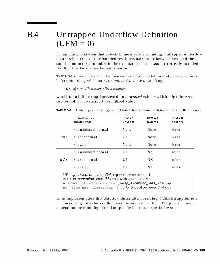
B.4 Untrapped Underflow Definition (UFM = 0)On an implementation that detects tininess before rounding, untrapped underflow occurs when the exact unrounded result has magnitude between zero and the smallest normalized number in the destination format and the correctly rounded result in the destination format is inexact.
TABLE B-2 summarizes what happens on an implementation that detects tininess before rounding, when an exact unrounded value u satisfying
0 ≤ |u| ≤ smallest normalized number
would round, if no trap intervened, to a rounded value r which might be zero, subnormal, or the smallest normalized value.
In an implementation that detects tininess after rounding, TABLE B-2 applies to a narrower range of values of the exact unrounded result u. The precise bounds depend on the rounding direction specified in FSR.RD, as follows:
TABLE B-2 Untrapped Floating-Point Underflow (Tininess Detected Before Rounding)
Underflow trap:Inexact trap:
UFM = 1NXM = x
UFM = 0NXM = 1
UFM = 0 NXM = 0
u = r
r is minimum normal None None None
r is subnormal UF None None
r is zero None None None
u ≠ r
r is minimum normal UF NX uf nx
r is subnormal UF NX uf nx
r is zero UF NX uf nx
UF = fp_exception_ieee_754 trap with cexc.ufc = 1 NX = fp_exception_ieee_754 trap with cexc.nxc = 1 uf = cexc.ufc = 1, aexc.ufa = 1, no fp_exception_ieee_754 trap nx = cexc.nxc = 1, aexc.nxa = 1, no fp_exception_ieee_754 trap
Release 1.0.4, 31 May 2002 C. Appendix B • IEEE Std 754-1985 Requirements for SPARC V9 395
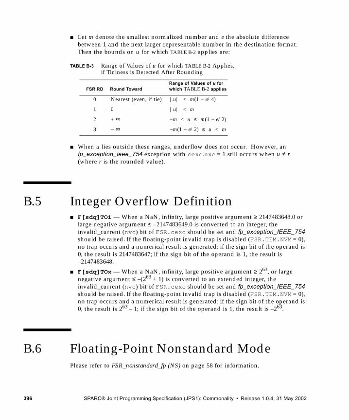
■ Let m denote the smallest normalized number and e the absolute difference between 1 and the next larger representable number in the destination format. Then the bounds on u for which TABLE B-2 applies are:
■ When u lies outside these ranges, underflow does not occur. However, an fp_exception_ieee_754 exception with cexc.nxc = 1 still occurs when u ≠ r (where r is the rounded value).
B.5 Integer Overflow Definition■ F[sdq]TOi — When a NaN, infinity, large positive argument ≥ 2147483648.0 or
large negative argument ≤ –2147483649.0 is converted to an integer, the invalid_current (nvc) bit of FSR.cexc should be set and fp_exception_IEEE_754 should be raised. If the floating-point invalid trap is disabled (FSR.TEM.NVM = 0), no trap occurs and a numerical result is generated: if the sign bit of the operand is 0, the result is 2147483647; if the sign bit of the operand is 1, the result is –2147483648.
■ F[sdq]TOx — When a NaN, infinity, large positive argument ≥ 263, or large negative argument ≤ –(263 + 1) is converted to an extended integer, the invalid_current (nvc) bit of FSR.cexc should be set and fp_exception_IEEE_754 should be raised. If the floating-point invalid trap is disabled (FSR.TEM.NVM = 0), no trap occurs and a numerical result is generated: if the sign bit of the operand is 0, the result is 263 – 1; if the sign bit of the operand is 1, the result is –263.
B.6 Floating-Point Nonstandard ModePlease refer to FSR_nonstandard_fp (NS) on page 58 for information.
TABLE B-3 Range of Values of u for which TABLE B-2 Applies, if Tininess is Detected After Rounding
FSR.RD Round TowardRange of Values of u for which TABLE B-2 applies
0 Nearest (even, if tie) |u| < m(1 − e/4)
1 0 |u| < m
2 + ∞ −m < u ≤ m(1 − e/2)
3 − ∞ −m(1 − e/2) ≤ u < m
396 SPARC® Joint Programming Specification (JPS1): Commonality • Release 1.0.4, 31 May 2002
C.APPENDIX C
Implementation Dependencies
This appendix summarizes implementation dependencies in the SPARC V9 standard. In SPARC V9, the notation “IMPL. DEP. #nn:” identifies the definition of an implementation dependency; the notation “(impl. dep. #nn)” identifies a reference to an implementation dependency. These dependencies are described by their number nn in TABLE C-1 on page 399.
The appendix contains these sections:
■ Definition of an Implementation Dependency on page 398■ Hardware Characteristics on page 398■ Implementation Dependency Categories on page 399■ List of Implementation Dependencies on page 399
Note – SPARC International maintains a document, Implementation Characteristics of Current SPARC-V9-based Products, Revision 9.x, that describes the implementation-dependent design features of all SPARC V9-compliant implementations. Contact SPARC International for this document at:
home page: www.sparc.orgemail: [email protected]
Release 1.0.4, 31 May 2002 C. Appendix C • Implementation Dependencies 397
C.1 Definition of an Implementation DependencyThe SPARC V9 architecture is a model that specifies unambiguously the behavior observed by software on SPARC V9 systems. Therefore, it does not necessarily describe the operation of the hardware of any actual implementation.
An implementation is not required to execute every instruction in hardware. An attempt to execute a SPARC V9 instruction that is not implemented in hardware generates a trap. Whether an instruction is implemented directly by hardware, simulated by software, or emulated by firmware is implementation dependent.
The two levels of SPARC V9 compliance are described in SPARC V9 Compliance on page 8.
Some elements of the architecture are defined to be implementation dependent. These elements include certain registers and operations that may vary from implementation to implementation; they are explicitly identified as such in this appendix.
Implementation elements (such as instructions or registers) that appear in an implementation but are not defined in this document (or its updates) are not considered to be SPARC V9 elements of that implementation.
C.2 Hardware CharacteristicsHardware characteristics that do not affect the behavior observed by software on SPARC V9 systems are not considered architectural implementation dependencies. A hardware characteristic may be relevant to the user system design (for example, the speed of execution of an instruction) or may be transparent to the user (for example, the method used for achieving cache consistency). The SPARC International document, Implementation Characteristics of Current SPARC-V9-based Products, Revision 9.x, provides a useful list of these hardware characteristics, along with the list of implementation-dependent design features of SPARC V9-compliant implementations.
In general, hardware characteristics deal with
■ Instruction execution speed
■ Whether instructions are implemented in hardware
■ The nature and degree of concurrency of the various hardware units constituting a SPARC V9 implementation
398 SPARC® Joint Programming Specification (JPS1): Commonality • Release 1.0.4, 31 May 2002
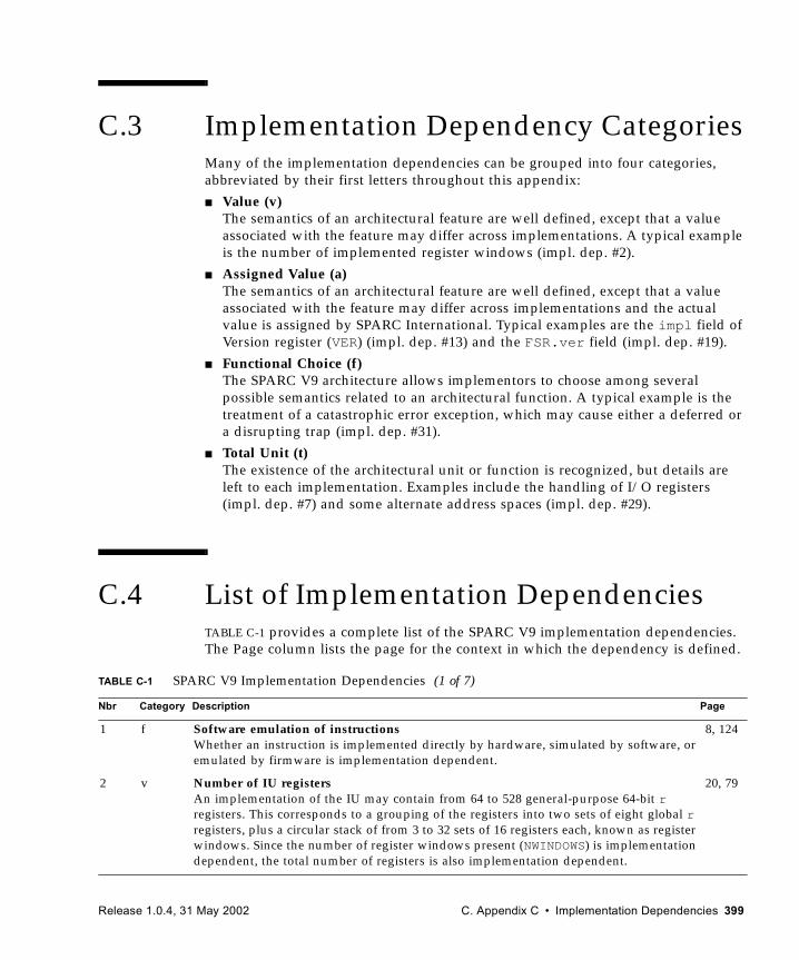
C.3 Implementation Dependency CategoriesMany of the implementation dependencies can be grouped into four categories, abbreviated by their first letters throughout this appendix:
■ Value (v) The semantics of an architectural feature are well defined, except that a value associated with the feature may differ across implementations. A typical example is the number of implemented register windows (impl. dep. #2).
■ Assigned Value (a)The semantics of an architectural feature are well defined, except that a value associated with the feature may differ across implementations and the actual value is assigned by SPARC International. Typical examples are the impl field of Version register (VER) (impl. dep. #13) and the FSR.ver field (impl. dep. #19).
■ Functional Choice (f)The SPARC V9 architecture allows implementors to choose among several possible semantics related to an architectural function. A typical example is the treatment of a catastrophic error exception, which may cause either a deferred or a disrupting trap (impl. dep. #31).
■ Total Unit (t)The existence of the architectural unit or function is recognized, but details are left to each implementation. Examples include the handling of I/O registers (impl. dep. #7) and some alternate address spaces (impl. dep. #29).
C.4 List of Implementation DependenciesTABLE C-1 provides a complete list of the SPARC V9 implementation dependencies. The Page column lists the page for the context in which the dependency is defined.
TABLE C-1 SPARC V9 Implementation Dependencies (1 of 7)
Nbr Category Description Page
1 f Software emulation of instructionsWhether an instruction is implemented directly by hardware, simulated by software, or emulated by firmware is implementation dependent.
8, 124
2 v Number of IU registersAn implementation of the IU may contain from 64 to 528 general-purpose 64-bit r registers. This corresponds to a grouping of the registers into two sets of eight global r registers, plus a circular stack of from 3 to 32 sets of 16 registers each, known as register windows. Since the number of register windows present (NWINDOWS) is implementation dependent, the total number of registers is also implementation dependent.
20, 79
Release 1.0.4, 31 May 2002 C. Appendix C • Implementation Dependencies 399
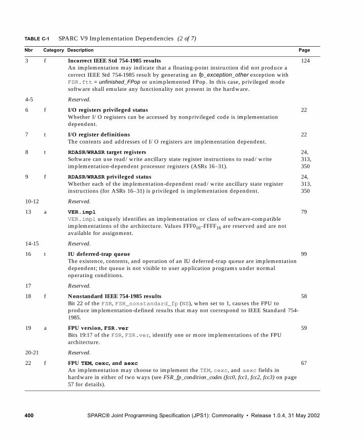
3 f Incorrect IEEE Std 754-1985 resultsAn implementation may indicate that a floating-point instruction did not produce a correct IEEE Std 754-1985 result by generating an fp_exception_other exception with FSR.ftt = unfinished_FPop or unimplemented FPop. In this case, privileged mode software shall emulate any functionality not present in the hardware.
124
4-5 Reserved.
6 f I/O registers privileged statusWhether I/O registers can be accessed by nonprivileged code is implementation dependent.
22
7 t I/O register definitionsThe contents and addresses of I/O registers are implementation dependent.
22
8 t RDASR/WRASR target registersSoftware can use read/write ancillary state register instructions to read/write implementation-dependent processor registers (ASRs 16–31).
24, 313, 350
9 f RDASR/WRASR privileged statusWhether each of the implementation-dependent read/write ancillary state register instructions (for ASRs 16–31) is privileged is implementation dependent.
24, 313, 350
10-12 Reserved.
13 a VER.implVER.impl uniquely identifies an implementation or class of software-compatible implementations of the architecture. Values FFF016–FFFF16 are reserved and are not available for assignment.
79
14-15 Reserved.
16 t IU deferred-trap queueThe existence, contents, and operation of an IU deferred-trap queue are implementation dependent; the queue is not visible to user application programs under normal operating conditions.
99
17 Reserved.
18 f Nonstandard IEEE 754-1985 resultsBit 22 of the FSR, FSR_nonstandard_fp (NS), when set to 1, causes the FPU to produce implementation-defined results that may not correspond to IEEE Standard 754-1985.
58
19 a FPU version, FSR.verBits 19:17 of the FSR, FSR.ver, identify one or more implementations of the FPU architecture.
59
20-21 Reserved.
22 f FPU TEM, cexc, and aexcAn implementation may choose to implement the TEM, cexc, and aexc fields in hardware in either of two ways (see FSR_fp_condition_codes (fcc0, fcc1, fcc2, fcc3) on page 57 for details).
67
TABLE C-1 SPARC V9 Implementation Dependencies (2 of 7)
Nbr Category Description Page
400 SPARC® Joint Programming Specification (JPS1): Commonality • Release 1.0.4, 31 May 2002
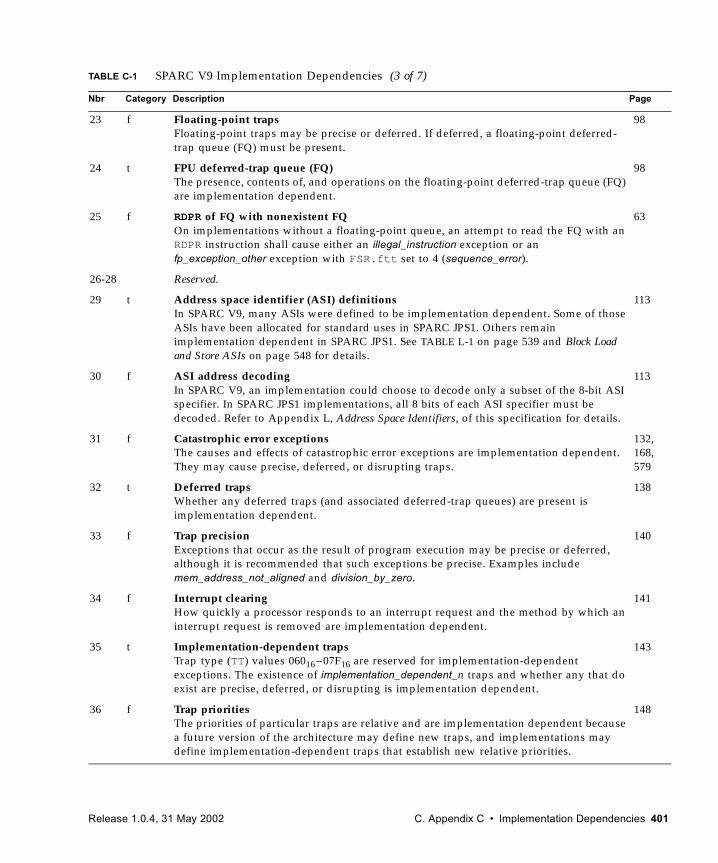
23 f Floating-point trapsFloating-point traps may be precise or deferred. If deferred, a floating-point deferred-trap queue (FQ) must be present.
98
24 t FPU deferred-trap queue (FQ)The presence, contents of, and operations on the floating-point deferred-trap queue (FQ) are implementation dependent.
98
25 f RDPR of FQ with nonexistent FQOn implementations without a floating-point queue, an attempt to read the FQ with an RDPR instruction shall cause either an illegal_instruction exception or an fp_exception_other exception with FSR.ftt set to 4 (sequence_error).
63
26-28 Reserved.
29 t Address space identifier (ASI) definitionsIn SPARC V9, many ASIs were defined to be implementation dependent. Some of those ASIs have been allocated for standard uses in SPARC JPS1. Others remain implementation dependent in SPARC JPS1. See TABLE L-1 on page 539 and Block Load and Store ASIs on page 548 for details.
113
30 f ASI address decodingIn SPARC V9, an implementation could choose to decode only a subset of the 8-bit ASI specifier. In SPARC JPS1 implementations, all 8 bits of each ASI specifier must be decoded. Refer to Appendix L, Address Space Identifiers, of this specification for details.
113
31 f Catastrophic error exceptionsThe causes and effects of catastrophic error exceptions are implementation dependent. They may cause precise, deferred, or disrupting traps.
132, 168, 579
32 t Deferred trapsWhether any deferred traps (and associated deferred-trap queues) are present is implementation dependent.
138
33 f Trap precisionExceptions that occur as the result of program execution may be precise or deferred, although it is recommended that such exceptions be precise. Examples include mem_address_not_aligned and division_by_zero.
140
34 f Interrupt clearingHow quickly a processor responds to an interrupt request and the method by which an interrupt request is removed are implementation dependent.
141
35 t Implementation-dependent trapsTrap type (TT) values 06016 –07F16 are reserved for implementation-dependent exceptions. The existence of implementation_dependent_n traps and whether any that do exist are precise, deferred, or disrupting is implementation dependent.
143
36 f Trap prioritiesThe priorities of particular traps are relative and are implementation dependent because a future version of the architecture may define new traps, and implementations may define implementation-dependent traps that establish new relative priorities.
148
TABLE C-1 SPARC V9 Implementation Dependencies (3 of 7)
Nbr Category Description Page
Release 1.0.4, 31 May 2002 C. Appendix C • Implementation Dependencies 401
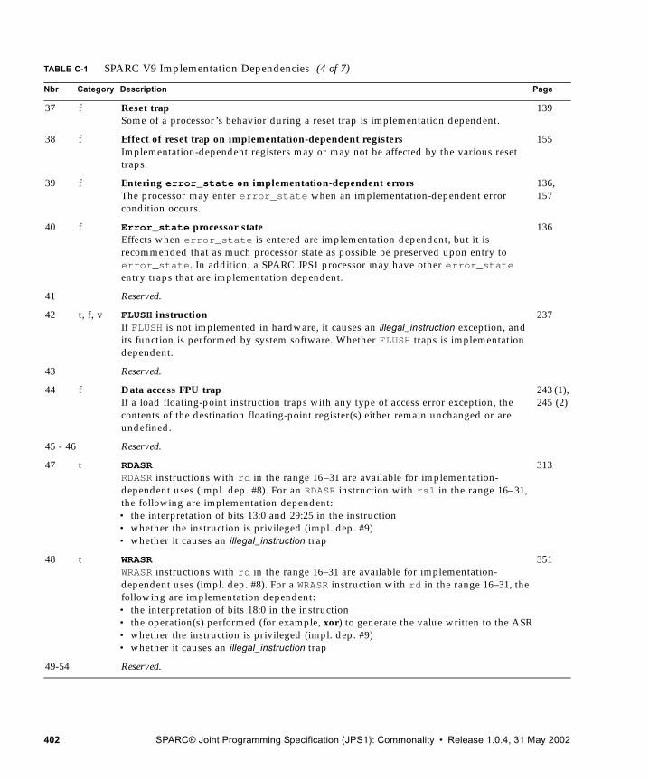
37 f Reset trapSome of a processor’s behavior during a reset trap is implementation dependent.
139
38 f Effect of reset trap on implementation-dependent registersImplementation-dependent registers may or may not be affected by the various reset traps.
155
39 f Entering error_state on implementation-dependent errorsThe processor may enter error_state when an implementation-dependent error condition occurs.
136, 157
40 f Error_state processor stateEffects when error_state is entered are implementation dependent, but it is recommended that as much processor state as possible be preserved upon entry to error_state. In addition, a SPARC JPS1 processor may have other error_state entry traps that are implementation dependent.
136
41 Reserved.
42 t, f, v FLUSH instructionIf FLUSH is not implemented in hardware, it causes an illegal_instruction exception, and its function is performed by system software. Whether FLUSH traps is implementation dependent.
237
43 Reserved.
44 f Data access FPU trapIf a load floating-point instruction traps with any type of access error exception, the contents of the destination floating-point register(s) either remain unchanged or are undefined.
243 (1), 245 (2)
45 - 46 Reserved.
47 t RDASRRDASR instructions with rd in the range 16–31 are available for implementation-dependent uses (impl. dep. #8). For an RDASR instruction with rs1 in the range 16–31, the following are implementation dependent:• the interpretation of bits 13:0 and 29:25 in the instruction• whether the instruction is privileged (impl. dep. #9)• whether it causes an illegal_instruction trap
313
48 t WRASRWRASR instructions with rd in the range 16–31 are available for implementation-dependent uses (impl. dep. #8). For a WRASR instruction with rd in the range 16–31, the following are implementation dependent:• the interpretation of bits 18:0 in the instruction• the operation(s) performed (for example, xor) to generate the value written to the ASR• whether the instruction is privileged (impl. dep. #9)• whether it causes an illegal_instruction trap
351
49-54 Reserved.
TABLE C-1 SPARC V9 Implementation Dependencies (4 of 7)
Nbr Category Description Page
402 SPARC® Joint Programming Specification (JPS1): Commonality • Release 1.0.4, 31 May 2002
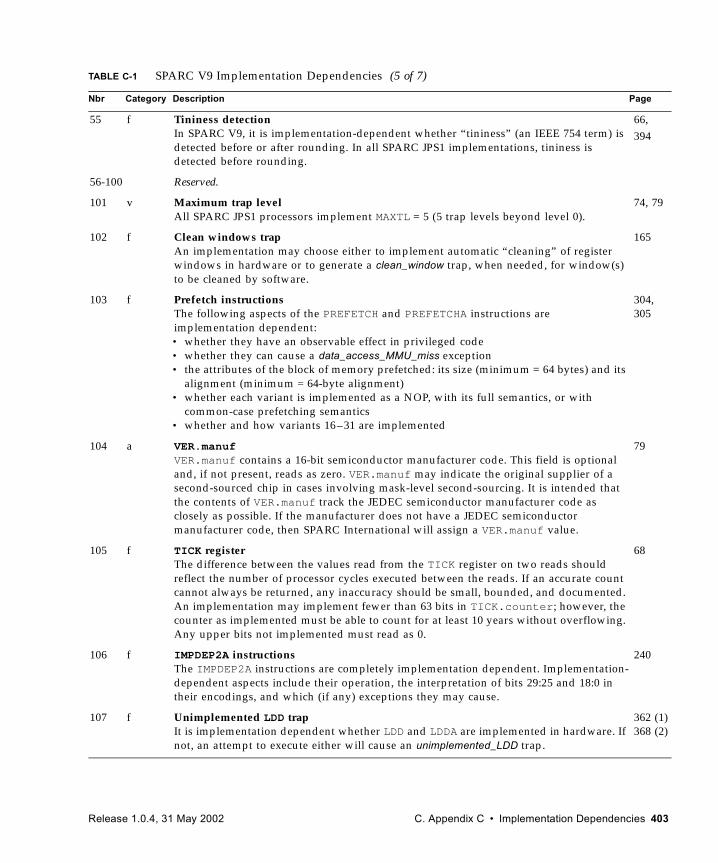
55 f Tininess detectionIn SPARC V9, it is implementation-dependent whether “tininess” (an IEEE 754 term) is detected before or after rounding. In all SPARC JPS1 implementations, tininess is detected before rounding.
66,394
56-100 Reserved.
101 v Maximum trap levelAll SPARC JPS1 processors implement MAXTL = 5 (5 trap levels beyond level 0).
74, 79
102 f Clean windows trapAn implementation may choose either to implement automatic “cleaning” of register windows in hardware or to generate a clean_window trap, when needed, for window(s) to be cleaned by software.
165
103 f Prefetch instructionsThe following aspects of the PREFETCH and PREFETCHA instructions are implementation dependent: • whether they have an observable effect in privileged code• whether they can cause a data_access_MMU_miss exception• the attributes of the block of memory prefetched: its size (minimum = 64 bytes) and its
alignment (minimum = 64-byte alignment)• whether each variant is implemented as a NOP, with its full semantics, or with
common-case prefetching semantics• whether and how variants 16–31 are implemented
304, 305
104 a VER.manufVER.manuf contains a 16-bit semiconductor manufacturer code. This field is optional and, if not present, reads as zero. VER.manuf may indicate the original supplier of a second-sourced chip in cases involving mask-level second-sourcing. It is intended that the contents of VER.manuf track the JEDEC semiconductor manufacturer code as closely as possible. If the manufacturer does not have a JEDEC semiconductor manufacturer code, then SPARC International will assign a VER.manuf value.
79
105 f TICK registerThe difference between the values read from the TICK register on two reads should reflect the number of processor cycles executed between the reads. If an accurate count cannot always be returned, any inaccuracy should be small, bounded, and documented. An implementation may implement fewer than 63 bits in TICK.counter; however, the counter as implemented must be able to count for at least 10 years without overflowing. Any upper bits not implemented must read as 0.
68
106 f IMPDEP2A instructionsThe IMPDEP2A instructions are completely implementation dependent. Implementation-dependent aspects include their operation, the interpretation of bits 29:25 and 18:0 in their encodings, and which (if any) exceptions they may cause.
240
107 f Unimplemented LDD trapIt is implementation dependent whether LDD and LDDA are implemented in hardware. If not, an attempt to execute either will cause an unimplemented_LDD trap.
362 (1)368 (2)
TABLE C-1 SPARC V9 Implementation Dependencies (5 of 7)
Nbr Category Description Page
Release 1.0.4, 31 May 2002 C. Appendix C • Implementation Dependencies 403
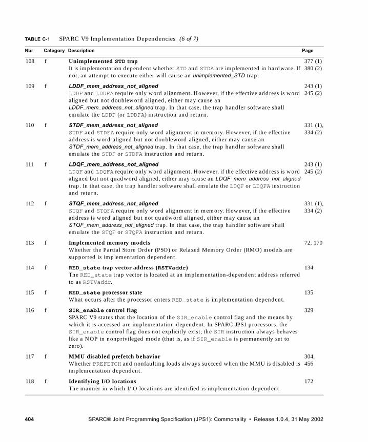
108 f Unimplemented STD trapIt is implementation dependent whether STD and STDA are implemented in hardware. If not, an attempt to execute either will cause an unimplemented_STD trap.
377 (1)380 (2)
109 f LDDF_mem_address_not_alignedLDDF and LDDFA require only word alignment. However, if the effective address is word aligned but not doubleword aligned, either may cause an LDDF_mem_address_not_aligned trap. In that case, the trap handler software shall emulate the LDDF (or LDDFA) instruction and return.
243 (1)245 (2)
110 f STDF_mem_address_not_alignedSTDF and STDFA require only word alignment in memory. However, if the effective address is word aligned but not doubleword aligned, either may cause an STDF_mem_address_not_aligned trap. In that case, the trap handler software shall emulate the STDF or STDFA instruction and return.
331 (1),334 (2)
111 f LDQF_mem_address_not_alignedLDQF and LDQFA require only word alignment. However, if the effective address is word aligned but not quadword aligned, either may cause an LDQF_mem_address_not_aligned trap. In that case, the trap handler software shall emulate the LDQF or LDQFA instruction and return.
243 (1)245 (2)
112 f STQF_mem_address_not_alignedSTQF and STQFA require only word alignment in memory. However, if the effective address is word aligned but not quadword aligned, either may cause an STQF_mem_address_not_aligned trap. In that case, the trap handler software shall emulate the STQF or STQFA instruction and return.
331 (1),334 (2)
113 f Implemented memory modelsWhether the Partial Store Order (PSO) or Relaxed Memory Order (RMO) models are supported is implementation dependent.
72, 170
114 f RED_state trap vector address (RSTVaddr)The RED_state trap vector is located at an implementation-dependent address referred to as RSTVaddr.
134
115 f RED_state processor stateWhat occurs after the processor enters RED_state is implementation dependent.
135
116 f SIR_enable control flagSPARC V9 states that the location of the SIR_enable control flag and the means by which it is accessed are implementation dependent. In SPARC JPS1 processors, the SIR_enable control flag does not explicitly exist; the SIR instruction always behaves like a NOP in nonprivileged mode (that is, as if SIR_enable is permanently set to zero).
329
117 f MMU disabled prefetch behaviorWhether PREFETCH and nonfaulting loads always succeed when the MMU is disabled is implementation dependent.
304, 456
118 f Identifying I/O locationsThe manner in which I/O locations are identified is implementation dependent.
172
TABLE C-1 SPARC V9 Implementation Dependencies (6 of 7)
Nbr Category Description Page
404 SPARC® Joint Programming Specification (JPS1): Commonality • Release 1.0.4, 31 May 2002
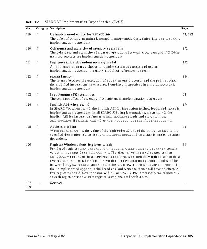
119 f Unimplemented values for PSTATE.MMThe effect of writing an unimplemented memory-mode designation into PSTATE.MM is implementation dependent.
72, 182
120 f Coherence and atomicity of memory operationsThe coherence and atomicity of memory operations between processors and I/O DMA memory accesses are implementation dependent.
172
121 f Implementation-dependent memory modelAn implementation may choose to identify certain addresses and use an implementation-dependent memory model for references to them.
172
122 f FLUSH latencyThe latency between the execution of FLUSH on one processor and the point at which the modified instructions have replaced outdated instructions in a multiprocessor is implementation dependent.
184
123 f Input/output (I/O) semanticsThe semantic effect of accessing I/O registers is implementation dependent.
22
124 v Implicit ASI when TL > 0In SPARC V9, when TL > 0, the implicit ASI for instruction fetches, loads, and stores is implementation dependent. In all SPARC JPS1 implementations, when TL > 0, the implicit ASI for instruction fetches is ASI_NUCLEUS; loads and stores will use ASI_NUCLEUS if PSTATE.CLE = 0 or ASI_NUCLEUS_LITTLE if PSTATE.CLE = 1.
174
125 f Address maskingWhen PSTATE.AM = 1, the value of the high-order 32-bits of the PC transmitted to the specified destination register(s) by CALL, JMPL, RDPC, and on a trap is implementation dependent.
73
126 Register Windows State Registers width Privileged registers CWP, CANSAVE, CANRESTORE, OTHERWIN, and CLEANWIN contain values in the range 0 to NWINDOWS − 1. The effect of writing a value greater than NWINDOWS − 1 to any of these registers is undefined. Although the width of each of these five registers is nominally 5 bits, the width is implementation dependent and shall be between log2(NWINDOWS) and 5 bits, inclusive. If fewer than 5 bits are implemented, the unimplemented upper bits shall read as 0 and writes to them shall have no effect. All five registers should have the same width. For SPARC JPS1 processors, NWINDOWS = 8, so each register window state register is implemented with 3 bits.
80
127-199
— Reserved. —
TABLE C-1 SPARC V9 Implementation Dependencies (7 of 7)
Nbr Category Description Page
Release 1.0.4, 31 May 2002 C. Appendix C • Implementation Dependencies 405
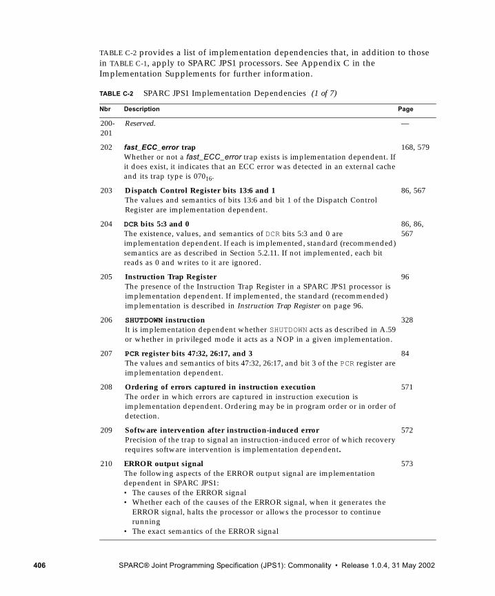
TABLE C-2 provides a list of implementation dependencies that, in addition to those in TABLE C-1, apply to SPARC JPS1 processors. See Appendix C in the Implementation Supplements for further information.
TABLE C-2 SPARC JPS1 Implementation Dependencies (1 of 7)
Nbr Description Page
200-201
Reserved. —
202 fast_ECC_error trapWhether or not a fast_ECC_error trap exists is implementation dependent. If it does exist, it indicates that an ECC error was detected in an external cache and its trap type is 07016.
168, 579
203 Dispatch Control Register bits 13:6 and 1The values and semantics of bits 13:6 and bit 1 of the Dispatch Control Register are implementation dependent.
86, 567
204 DCR bits 5:3 and 0The existence, values, and semantics of DCR bits 5:3 and 0 are implementation dependent. If each is implemented, standard (recommended) semantics are as described in Section 5.2.11. If not implemented, each bit reads as 0 and writes to it are ignored.
86, 86, 567
205 Instruction Trap RegisterThe presence of the Instruction Trap Register in a SPARC JPS1 processor is implementation dependent. If implemented, the standard (recommended) implementation is described in Instruction Trap Register on page 96.
96
206 SHUTDOWN instructionIt is implementation dependent whether SHUTDOWN acts as described in A.59 or whether in privileged mode it acts as a NOP in a given implementation.
328
207 PCR register bits 47:32, 26:17, and 3The values and semantics of bits 47:32, 26:17, and bit 3 of the PCR register are implementation dependent.
84
208 Ordering of errors captured in instruction executionThe order in which errors are captured in instruction execution is implementation dependent. Ordering may be in program order or in order of detection.
571
209 Software intervention after instruction-induced errorPrecision of the trap to signal an instruction-induced error of which recovery requires software intervention is implementation dependent.
572
210 ERROR output signalThe following aspects of the ERROR output signal are implementation dependent in SPARC JPS1:• The causes of the ERROR signal• Whether each of the causes of the ERROR signal, when it generates the
ERROR signal, halts the processor or allows the processor to continue running
• The exact semantics of the ERROR signal
573
406 SPARC® Joint Programming Specification (JPS1): Commonality • Release 1.0.4, 31 May 2002
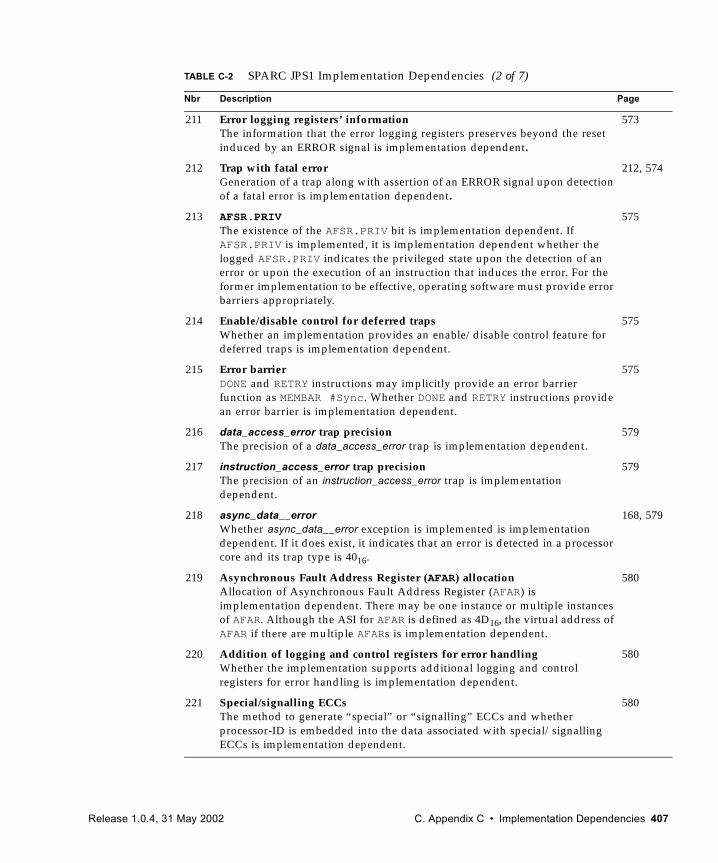
211 Error logging registers’ informationThe information that the error logging registers preserves beyond the reset induced by an ERROR signal is implementation dependent.
573
212 Trap with fatal errorGeneration of a trap along with assertion of an ERROR signal upon detection of a fatal error is implementation dependent.
212, 574
213 AFSR.PRIVThe existence of the AFSR.PRIV bit is implementation dependent. If AFSR.PRIV is implemented, it is implementation dependent whether the logged AFSR.PRIV indicates the privileged state upon the detection of an error or upon the execution of an instruction that induces the error. For the former implementation to be effective, operating software must provide error barriers appropriately.
575
214 Enable/disable control for deferred trapsWhether an implementation provides an enable/disable control feature for deferred traps is implementation dependent.
575
215 Error barrierDONE and RETRY instructions may implicitly provide an error barrier function as MEMBAR #Sync. Whether DONE and RETRY instructions provide an error barrier is implementation dependent.
575
216 data_access_error trap precisionThe precision of a data_access_error trap is implementation dependent.
579
217 instruction_access_error trap precisionThe precision of an instruction_access_error trap is implementation dependent.
579
218 async_data__errorWhether async_data__error exception is implemented is implementation dependent. If it does exist, it indicates that an error is detected in a processor core and its trap type is 4016.
168, 579
219 Asynchronous Fault Address Register (AFAR) allocationAllocation of Asynchronous Fault Address Register (AFAR) is implementation dependent. There may be one instance or multiple instances of AFAR. Although the ASI for AFAR is defined as 4D16, the virtual address of AFAR if there are multiple AFARs is implementation dependent.
580
220 Addition of logging and control registers for error handlingWhether the implementation supports additional logging and control registers for error handling is implementation dependent.
580
221 Special/signalling ECCsThe method to generate “special” or “signalling” ECCs and whether processor-ID is embedded into the data associated with special/signalling ECCs is implementation dependent.
580
TABLE C-2 SPARC JPS1 Implementation Dependencies (2 of 7)
Nbr Description Page
Release 1.0.4, 31 May 2002 C. Appendix C • Implementation Dependencies 407
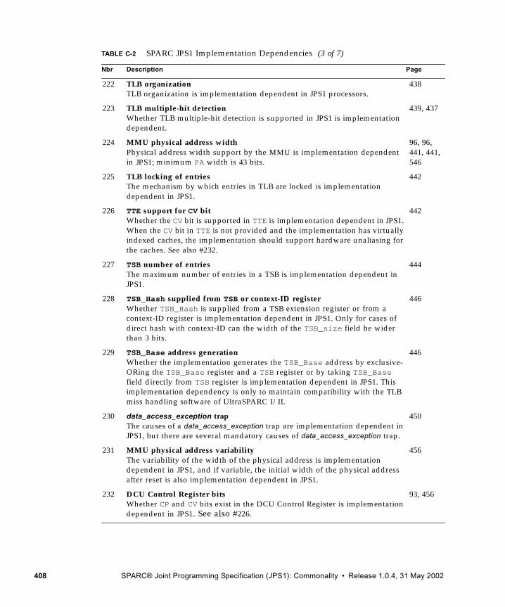
222 TLB organizationTLB organization is implementation dependent in JPS1 processors.
438
223 TLB multiple-hit detectionWhether TLB multiple-hit detection is supported in JPS1 is implementation dependent.
439, 437
224 MMU physical address widthPhysical address width support by the MMU is implementation dependent in JPS1; minimum PA width is 43 bits.
96, 96, 441, 441, 546
225 TLB locking of entriesThe mechanism by which entries in TLB are locked is implementation dependent in JPS1.
442
226 TTE support for CV bitWhether the CV bit is supported in TTE is implementation dependent in JPS1. When the CV bit in TTE is not provided and the implementation has virtually indexed caches, the implementation should support hardware unaliasing for the caches. See also #232.
442
227 TSB number of entriesThe maximum number of entries in a TSB is implementation dependent in JPS1.
444
228 TSB_Hash supplied from TSB or context-ID registerWhether TSB_Hash is supplied from a TSB extension register or from a context-ID register is implementation dependent in JPS1. Only for cases of direct hash with context-ID can the width of the TSB_size field be wider than 3 bits.
446
229 TSB_Base address generationWhether the implementation generates the TSB_Base address by exclusive-ORing the TSB_Base register and a TSB register or by taking TSB_Base field directly from TSB register is implementation dependent in JPS1. This implementation dependency is only to maintain compatibility with the TLB miss handling software of UltraSPARC I/II.
446
230 data_access_exception trapThe causes of a data_access_exception trap are implementation dependent in JPS1, but there are several mandatory causes of data_access_exception trap.
450
231 MMU physical address variabilityThe variability of the width of the physical address is implementation dependent in JPS1, and if variable, the initial width of the physical address after reset is also implementation dependent in JPS1.
456
232 DCU Control Register bitsWhether CP and CV bits exist in the DCU Control Register is implementation dependent in JPS1. See also #226.
93, 456
TABLE C-2 SPARC JPS1 Implementation Dependencies (3 of 7)
Nbr Description Page
408 SPARC® Joint Programming Specification (JPS1): Commonality • Release 1.0.4, 31 May 2002
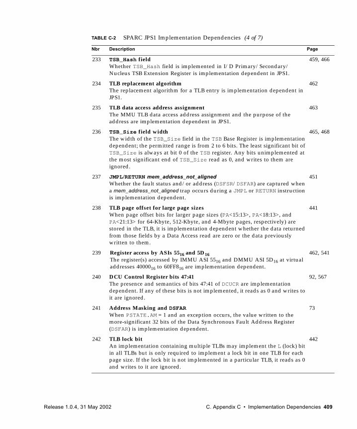
233 TSB_Hash fieldWhether TSB_Hash field is implemented in I/D Primary/Secondary/Nucleus TSB Extension Register is implementation dependent in JPS1.
459, 466
234 TLB replacement algorithmThe replacement algorithm for a TLB entry is implementation dependent in JPS1.
462
235 TLB data access address assignmentThe MMU TLB data access address assignment and the purpose of the address are implementation dependent in JPS1.
463
236 TSB_Size field widthThe width of the TSB_Size field in the TSB Base Register is implementation dependent; the permitted range is from 2 to 6 bits. The least significant bit of TSB_Size is always at bit 0 of the TSB register. Any bits unimplemented at the most significant end of TSB_Size read as 0, and writes to them are ignored.
465, 468
237 JMPL/RETURN mem_address_not_alignedWhether the fault status and/or address (DSFSR/DSFAR) are captured when a mem_address_not_aligned trap occurs during a JMPL or RETURN instruction is implementation dependent.
451
238 TLB page offset for large page sizesWhen page offset bits for larger page sizes (PA<15:13>, PA<18:13>, and PA<21:13> for 64-Kbyte, 512-Kbyte, and 4-Mbyte pages, respectively) are stored in the TLB, it is implementation dependent whether the data returned from those fields by a Data Access read are zero or the data previously written to them.
441
239 Register access by ASIs 5516 and 5D16The register(s) accessed by IMMU ASI 5516 and DMMU ASI 5D16 at virtual addresses 4000016 to 60FF816 are implementation dependent.
462, 541
240 DCU Control Register bits 47:41The presence and semantics of bits 47:41 of DCUCR are implementation dependent. If any of these bits is not implemented, it reads as 0 and writes to it are ignored.
92, 567
241 Address Masking and DSFARWhen PSTATE.AM = 1 and an exception occurs, the value written to the more-significant 32 bits of the Data Synchronous Fault Address Register (DSFAR) is implementation dependent.
73
242 TLB lock bitAn implementation containing multiple TLBs may implement the L (lock) bit in all TLBs but is only required to implement a lock bit in one TLB for each page size. If the lock bit is not implemented in a particular TLB, it reads as 0 and writes to it are ignored.
442
TABLE C-2 SPARC JPS1 Implementation Dependencies (4 of 7)
Nbr Description Page
Release 1.0.4, 31 May 2002 C. Appendix C • Implementation Dependencies 409
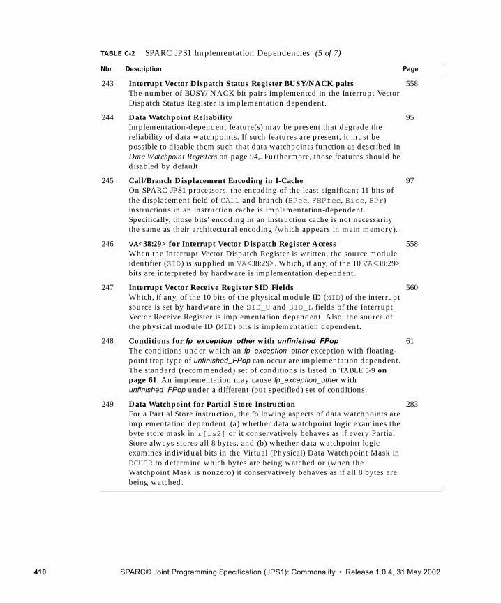
243 Interrupt Vector Dispatch Status Register BUSY/NACK pairsThe number of BUSY/NACK bit pairs implemented in the Interrupt Vector Dispatch Status Register is implementation dependent.
558
244 Data Watchpoint ReliabilityImplementation-dependent feature(s) may be present that degrade the reliability of data watchpoints. If such features are present, it must be possible to disable them such that data watchpoints function as described in Data Watchpoint Registers on page 94,. Furthermore, those features should be disabled by default
95
245 Call/Branch Displacement Encoding in I-CacheOn SPARC JPS1 processors, the encoding of the least significant 11 bits of the displacement field of CALL and branch (BPcc, FBPfcc, Bicc, BPr) instructions in an instruction cache is implementation-dependent. Specifically, those bits' encoding in an instruction cache is not necessarily the same as their architectural encoding (which appears in main memory).
97
246 VA<38:29> for Interrupt Vector Dispatch Register AccessWhen the Interrupt Vector Dispatch Register is written, the source module identifier (SID) is supplied in VA<38:29>. Which, if any, of the 10 VA<38:29> bits are interpreted by hardware is implementation dependent.
558
247 Interrupt Vector Receive Register SID FieldsWhich, if any, of the 10 bits of the physical module ID (MID) of the interrupt source is set by hardware in the SID_U and SID_L fields of the Interrupt Vector Receive Register is implementation dependent. Also, the source of the physical module ID (MID) bits is implementation dependent.
560
248 Conditions for fp_exception_other with unfinished_FPopThe conditions under which an fp_exception_other exception with floating-point trap type of unfinished_FPop can occur are implementation dependent. The standard (recommended) set of conditions is listed in TABLE 5-9 on page 61. An implementation may cause fp_exception_other with unfinished_FPop under a different (but specified) set of conditions.
61
249 Data Watchpoint for Partial Store InstructionFor a Partial Store instruction, the following aspects of data watchpoints are implementation dependent: (a) whether data watchpoint logic examines the byte store mask in r[rs2] or it conservatively behaves as if every Partial Store always stores all 8 bytes, and (b) whether data watchpoint logic examines individual bits in the Virtual (Physical) Data Watchpoint Mask in DCUCR to determine which bytes are being watched or (when the Watchpoint Mask is nonzero) it conservatively behaves as if all 8 bytes are being watched.
283
TABLE C-2 SPARC JPS1 Implementation Dependencies (5 of 7)
Nbr Description Page
410 SPARC® Joint Programming Specification (JPS1): Commonality • Release 1.0.4, 31 May 2002
250 PCR accessibility when PSTATE.PRIV = 0When the processor is operating in nonprivileged mode (PSTATE.PRIV = 0), the accessibility of PCR as a unit and of individual fields of PCR is implementation dependent. Also, which exception is raised upon detection of an access privilege violation is implementation dependent.
84, 85, 186, 314, 352
251 Reserved.
252 DCUCR.DC (Data Cache Enable)The presence of DCUCR bit 1 (DCUCR.DC, Data Cache Enable) is implementation dependent. If DC is not implemented, it reads as zero, writes to it are ignored, and software should only write zero or a value previously read from DC to DC. The remainder of this description assumes that DC is implemented. The function of DC is to enable/disable operation of the data cache closest to the processor (D-cache); DC = 1 enables the D-cache and DC = 0 disables it. When DC = 0, memory accesses (loads, stores, atomic load-stores) are satisfied by caches lower in the cache hierarchy. It is implementation dependent whether or not memory accesses update the D-cache while the D-cache is disabled (DC = 0). If memory accesses do not update the D-cache, then when the D-cache is reenabled (DC is set to 1) any D-cache lines still marked as “valid” may be inconsistent with the state of memory or other caches. In that case, software must handle any inconsistencies by flushing the inconsistent lines from the D-cache.
94
253 DCUCR.IC (Instruction Cache Enable)The presence of DCUCR bit 0 (DCUCR.IC, Instruction Cache Enable) is implementation dependent. If IC is not implemented, it reads as zero, writes to it are ignored, and software should only write zero or a value previously read from IC to IC. The remainder of this description assumes that IC is implemented. The function of IC is to enable/disable operation of the instruction cache closest to the processor (I-cache); IC = 1 enables the I-cache and IC = 0 disables it. When IC = 0, instruction fetches are satisfied by caches lower in the cache hierarchy. It is implementation dependent whether or not instruction fetches update the I-cache while the I-cache is disabled (IC = 0). If instruction fetches do not update the I-cache, then when the I-cache is reenabled (IC is set to 1) any I-cache lines still marked as “valid” may be inconsistent with the state of memory or other caches. In that case, software must handle any inconsistencies by invalidating the inconsistent lines in the I-cache.
94
254 Means of exiting error_stateThe means of exiting error_state are implementation dependent. A suggested method is for the processor, upon entering error_state, to automatically generate a watchdog_reset (WDR).
133, 136, 139, 157, 166, 563, 565
TABLE C-2 SPARC JPS1 Implementation Dependencies (6 of 7)
Nbr Description Page
Release 1.0.4, 31 May 2002 C. Appendix C • Implementation Dependencies 411
255 LDDFA with ASI E016 or E116 and misaligned destination register number For LDDFA with ASI E016 or E116, if a destination register number rd is specified which is not a multiple of 8 ("misaligned" rd), it is implementation dependent whether the processor generates a data_access_exception or illegal_instruction exception.
548
256 LDDFA with ASI E016 or E116 and misaligned memory address For LDDFA with ASI E016 or E116, if a memory address is specified with less than 64-byte alignment, it is implementation dependent whether the processor generates a data_access_exception, mem_address_not_aligned, or LDDF_mem_address_not_aligned exception.
548
257 LDDFA with ASI C016–C516 or C816–CD16 and misaligned memory address For LDDFA with ASI C016–C516 or C816–CD16, if a memory address is specified with less than 8-byte alignment, it is implementation dependent whether the processor generates a data_access_exception, mem_address_not_aligned, or LDDF_mem_address_not_aligned exception.
549
258 ASI_SERIAL_ID The semantics and encoding of ASI_SERIAL_ID are implementation dependent. Its intended use is for a part identification number that is unique to each chip.
541
TABLE C-2 SPARC JPS1 Implementation Dependencies (7 of 7)
Nbr Description Page
412 SPARC® Joint Programming Specification (JPS1): Commonality • Release 1.0.4, 31 May 2002
C.APPENDIX D
Formal Specification of the Memory Models
This appendix contains only material from The SPARC Architecture Manual, Version 9, which provides a formal description of the SPARC V9 processor’s interaction with memory. The formal description is more complete and more precise than the description of Chapter 8, Memory Models, and therefore represents the definitive specification. Implementations must conform to this model, and programmers must use this description to resolve any ambiguity.
This formal specification is not intended to be a description of an actual implementation, only to describe in a precise and rigorous fashion the behavior that any conforming implementation must provide.
D.1 Processors and MemoryThe system model consists of a collection of processors, P0, P1,…Pn-1. Each processor executes its own instruction stream.1 Processors may share address space and access to real memory and I/O locations.
To improve performance, processors may interpose a cache or caches in the path between the processor and memory. For data and I/O references, caches are required to be transparent. The memory model specifies the functional behavior of the entire memory subsystem, which includes any form of caching. Implementations must use appropriate cache coherency mechanisms to achieve this transparency.2
1. Processors are equivalent to their software abstraction, processes, provided that context switching is properly performed. See Appendix J, Programming with the Memory Models, for an example of context switch code.
2. Philip Bitar and Alvin M. Despain, “Multiprocessor Cache Synchronization: Issues, Innovations, Evolution,” Proc. 13th Annual International Symposium on Computer Architecture, Computer Architecture News 14:2, June 1986, pp.424-433.
Release 1.0.4, 31 May 2002 C. Appendix D • Formal Specification of the Memory Models 413
The SPARC V9 memory model requires that all data references be consistent but does not require that instruction references or input/output references be maintained consistent. The FLUSH instruction or an appropriate operating system call may be used to ensure that instruction and data spaces are consistent. Likewise, system software is needed to manage the consistency of I/O operations.
The memory model is a local property of a processor that determines the order properties of memory references. The ordering properties have global implications when memory is shared, since the memory model determines what data is visible to observing processors and in what order. Moreover, the operative memory model of the observing processor affects the apparent order of shared data reads and writes that it observes.
D.2 Overview of the Memory Model SpecificationThe underlying goal of the memory model is to place the weakest possible constraints on the processor implementations and to provide a precise specification of the possible orderings of memory operations so that shared-memory multiprocessors can be constructed.
An execution trace is a sequence of instructions with a specified initial instruction. An execution trace constitutes one possible execution of a program and may involve arbitrary reorderings and parallel execution of instructions. A self-consistent execution trace is one that generates precisely the same results as those produced by a program order execution trace.
A program order execution trace is an execution trace that begins with a specified initial instruction and executes one instruction at a time in such a fashion that all the semantic effects of each instruction take effect before the next instruction is begun. The execution trace this process generates is defined to be program order.
A program is defined by the collection of all possible program order execution traces.
Dependence order is a partial order on the instructions in an execution trace that is adequate to ensure that the execution trace is self-consistent. Dependence order can be constructed with conventional data dependence analysis techniques. Dependence order holds only between instructions in the instruction trace of a single processor; instructions that are part of execution traces on different processors are never dependence ordered.
Memory order is a total order on the memory reference instructions (loads, stores, and atomic load/stores) which satisfies the dependence order and, possibly, other order constraints such as those introduced implicitly by the choice of memory model or
414 SPARC® Joint Programming Specification (JPS1): Commonality • Release 1.0.4, 31 May 2002
explicitly by the appearance of memory barrier (MEMBAR) instructions in the execution trace. The existence of a global memory order on the performance of all stores implies that memory access is write-atomic.1
A memory model is a set of rules that constrains the order of memory references. The SPARC V9 architecture supports three memory models: Total Store Order (TSO), Partial Store Order (PSO), and Relaxed Memory Order (RMO). The memory models are defined only for memory and not for I/O locations. See Memory, Real Memory, and I/O Locations on page 171 for more information.
The formal definition used in the SPARC V8 specification2 remains valid for the definition of PSO and TSO, except for the FLUSH instruction, which has been modified slightly.3 The SPARC V9 architecture introduces a new memory model, RMO, which differs from TSO and PSO in that it allows load operations to be reordered as long as single-thread programs remain self-consistent.
D.3 Memory Transactions
D.3.1 Memory TransactionsA memory transaction is one of the following:
■ Store — A request by a processor to replace the value of a specified memory location. The address and new value are bound to the store transaction when the processor initiates the store transaction. A store is complete when the new value is visible to all processors in the system.
■ Load — A request by a processor to retrieve the value of the specified memory location. The address is bound to the load transaction when the processor initiates the load transaction. A load is complete when the value being returned cannot be modified by a store made by another processor.
1. W.W. Collier, Reasoning About Parallel Architectures, Prentice-Hall, 1992, includes an excellent discussion of write-atomicity and related memory model topics.
2. Pradeep Sindhu, Jean-Marc Frailong, and Michel Ceklov. “Formal Specification of Memory Models,” Xerox Palo Alto Research Center Report CSL-91-11, December 1991.
3. In SPARC V8, a FLUSH instruction needs at least five instruction execution cycles before it is guaranteed to have local effects; in SPARC V9 this five-cycle requirement has been removed.
Release 1.0.4, 31 May 2002 C. Appendix D • Formal Specification of the Memory Models 415
■ Atomic — A load/store pair with the guarantee that no other memory transaction will alter the state of the memory between the load and the store. The SPARC V9 instruction set includes three atomic instructions: LDSTUB, SWAP, and CAS.1 An atomic transaction is considered to be both a load and a store.2
■ Flush — A request by a processor to force changes in the data space aliased to the instruction space to become consistent. Flush transactions are considered to be store operations for memory model purposes.
Memory transactions are referred to by capital letters: Xna, which denotes a specific memory transaction X by processor n to memory address a. The processor index and the address are specified only if needed. The predicate S(X) is true if and only if X has store semantics. The predicate L(X) is true if and only if X has load semantics.
MEMBAR instructions are not memory transactions; rather they convey order information above and beyond the implicit ordering implied by the memory model in use. MEMBAR instructions are applied in program order.
D.3.2 Program OrderThe program order is a per-processor total order that denotes the sequence in which processor n logically executes instructions. The program order relation is denoted by <p such that Xn <p Yn is true if and only if the memory transaction Xn is caused by an instruction that is executed before the instruction that caused memory transaction Yn.
Program order specifies a unique total order for all memory transactions initiated by one processor.
Memory barrier (MEMBAR) instructions executed by the processor are ordered with respect to <p. The predicate M(X,Y) is true if and only if X <p Y and there exists a MEMBAR instruction that orders X and Y (that is, it appears in program order between X and Y). MEMBAR instructions can be either ordering or sequencing and may be combined into a single instruction by a bit-encoded mask.3
Ordering MEMBAR instructions impose constraints on the order in which memory transactions are performed.
1. There are three generic forms. CASA and CASXA reference 32-bit and 64-bit objects, respectively. Both normal and alternate ASI forms exist for LDSTUB and SWAP. CASA and CASXA only have alternate forms; however, a CASA (CASXA) with ASI = ASI_PRIMARY{_LITTLE} is equivalent to CAS (CASX). Synthetic instructions for CAS and CASX are suggested in G.3, Synthetic Instructions.
2. Even though the store part of a CASA is conditional, it is assumed that the store will always take place whether or not it does in a particular implementation. Since the value stored when the condition fails is the value already present and since the CASA operation is atomic, no observing processor can determine whether the store occurred or not.
3. The Ordering MEMBAR instruction uses 4 bits of its argument to specify the existence of an order relation depending on whether X and Y have load or store semantics. The Sequencing MEMBAR uses three bits to specify completion conditions. The MEMBAR encoding is specified in A.35.
416 SPARC® Joint Programming Specification (JPS1): Commonality • Release 1.0.4, 31 May 2002
Sequencing MEMBARs introduce additional constraints that are required in cases where the memory transaction has side effects beyond storing data. Such side effects are beyond the scope of the memory model, which is limited to order and value semantics for memory.1
This definition of program order is equivalent to the definition given in the SPARC V8 memory model specification.
D.3.3 Dependence OrderDependence order is a partial order that captures the constraints that hold between instructions that access the same processor register or memory location. To allow maximum concurrency in processor implementations, dependence order assumes that registers are dynamically renamed to avoid false dependences arising from register reuse.
Two memory transactions X and Y are dependence ordered, denoted by X <d Y, if and only if they are program ordered, X <p Y, and at least one of the following conditions is true:
1. The execution of Y is conditional on X, and S(Y) is true.
2. Y reads a register that is written by X.
3. X and Y access the same memory location and S(X) and L(Y) are both true.
The dependence order also holds between the memory transactions associated with the instructions. It is important to remember that partial ordering is transitive.
Rule (1) includes all control dependences that arise from the dynamic execution of programs. In particular, a store or atomic memory transaction that is executed after a conditional branch will depend on the outcome of that branch instruction, which in turn will depend on one or more memory transactions that precede the branch instruction. Loads after an unresolved conditional branch may proceed, that is, a conditional branch does not dependence-order subsequent loads. Control dependences always order the initiation of subsequent instructions to the performance of the preceding instructions.2
Rule (2) captures dependences arising from register use. It is not necessary to include an ordering when X reads a register that is later written by Y, because register renaming will allow out-of-order execution in this case. Register renaming is equivalent to having an infinite pool of registers and requiring all registers to be
1. Sequencing constraints have other effects, such as controlling when a memory error is recognized or when an I/O access reaches global visibility. The need for sequencing constraints is always associated with I/O and kernel-level programming and not usually with normal, user-level application programming.
2. Self-modifying code (use of FLUSH instructions) also causes control dependences.
Release 1.0.4, 31 May 2002 C. Appendix D • Formal Specification of the Memory Models 417
write-once. Observe that the condition code register is set by some arithmetic and logical instructions and used by conditional branch instructions, thus introducing a dependence order.
Rule (3) captures ordering constraints resulting from memory accesses to the same location and requires that the dependence order reflect the program order for store-load pairs, but not for load-store or store-store pairs. A load may be executed speculatively since loads are side-effect free, provided that Rule (3) is eventually satisfied.
An actual processor implementation will maintain dependence order by score-boarding, hardware interlocks, data flow techniques, compiler-directed code scheduling, and so forth, or, simply, by sequential program execution. The means by which the dependence order is derived from a program is irrelevant to the memory model, which has to specify which possible memory transaction sequences are legal for a given set of data dependences. Practical implementations will not necessarily use the minimal set of constraints: adding unnecessary order relations from the program order to the dependence order only reduces the available concurrency but does not impair correctness.
D.3.4 Memory OrderThe sequence in which memory transactions are performed by the memory is called memory order, which is a total order on all memory transactions.
In general, the memory order cannot be known a priori. Instead, the memory order is specified as a set of constraints that are imposed on the memory transactions. The requirement that memory transaction X must be performed before memory transaction Y is denoted by X <m Y. Any memory order that satisfies these constraints is legal. The memory subsystem may choose arbitrarily among legal memory orders; hence, multiple executions of the same programs may result in different memory orders.
D.4 Specification of Relaxed Memory Order (RMO)
D.4.1 Value AtomicityMemory transactions will atomically set or retrieve the value of a memory location as long as the size of the value is less than or equal to eight bytes, the unit of coherency.
418 SPARC® Joint Programming Specification (JPS1): Commonality • Release 1.0.4, 31 May 2002
D.4.2 Store AtomicityAll possible execution traces are consistent with the existence of a memory order that totally orders all transactions including all store operations.
This does not imply that the memory order is observable. Nor does it imply that RMO requires any central serialization mechanism.
D.4.3 Atomic Memory TransactionsThe atomic memory transactions SWAP, LDSTUB, and CAS are performed as one memory transaction that is both a load and a store with respect to memory order constraints. No other memory transaction can separate the load and store actions of an atomic memory transaction. The semantics of atomic instructions are defined in Appendix A, Instruction Definitions.
D.4.4 Memory Order ConstraintsA memory order is legal in RMO if and only if:
1. X <d Y & L(X) ⇒ X <m Y
2. M(X,Y) ⇒ X <m Y
3. Xa <p Ya & S(Y) ⇒ X <m Y
Rule (1) states that the RMO model will maintain dependence when the preceding transaction is a load. Preceding stores may be delayed in the implementation, so their order may not be preserved globally.
Rule (2) states that MEMBAR instructions order the performance of memory transactions.
Rule (3) states that stores to the same address are performed in program order. This is necessary for processor self-consistency
D.4.5 Value of Memory TransactionsThe value of a load Ya is the value of the most recent store that was performed with respect to memory order or the value of the most recently initiated store by the same processor. Assuming Y is a load to memory location a:
Release 1.0.4, 31 May 2002 C. Appendix D • Formal Specification of the Memory Models 419
Value(La) = Value( Max<m { S | Sa <m La or Sa <p La } )
where Max<m{..} selects the most recent element with respect to the memory order and where Value() yields the value of a particular memory transaction. This states that the value returned by a load is either the result of the most recent store to that address which has been performed by any processor or which has been initiated by the processor issuing the load. The distinction between local and remote stores permits use of store buffers, which are explicitly supported in all SPARC V9 memory models.
D.4.6 Termination of Memory TransactionsAny memory transaction will eventually be performed. This is formalized by the requirement that only a finite number of memory ordered loads can be performed before a pending store is completed.
D.4.7 Flush Memory TransactionFlush instructions are treated as store memory transactions as far as the memory order is concerned. Their semantics are defined in Section A.22, Flush Instruction Memory. Flush instructions introduce a control dependence to any subsequent (in program order) execution of the instruction that was addressed by the flush.
D.5 Specification of Partial Store Order (PSO)The specification of Partial Store Order (PSO) is that of Relaxed Memory Order (RMO) with the additional requirement that all memory transactions with load semantics are followed by an implied MEMBAR #LoadLoad | #LoadStore.
D.6 Specification of Total Store Order (TSO)The specification of Total Store Order (TSO) is that of Partial Store Order (PSO) with the additional requirement that all memory transactions with store semantics are followed by an implied MEMBAR #StoreStore.
420 SPARC® Joint Programming Specification (JPS1): Commonality • Release 1.0.4, 31 May 2002
D.7 Examples of Program ExecutionsThis subsection lists several code sequences and an exhaustive list of all possible execution sequences under RMO, PSO, and TSO. For each example, the code is followed by the list of order relations between the corresponding memory transactions. The memory transactions are referred to by numbers. In each case, the program is executed once for each memory model.
D.7.1 Observation of Store AtomicityThe code example in FIGURE D-1 demonstrates how store atomicity prevents multiple processors from observing inconsistent sequences of events. In this case, processors 2 and 3 observe changes to the shared variables A and B, which are being modified by processor 1. Initially both variables are 0. The stores by processor 1 do not use any form of synchronization, and they may in fact be issued by two independent processors.
Should processor 2 find A to have the new value (1) and B to have the old value (0), it can infer that A was updated before B. Likewise, processor 3 may find B = 1 and A = 0, which implies that B was changed before A. It is impossible for both to occur in all SPARC V9 memory models since there cannot exist a total order on all stores. This property of the memory models has been encoded in the assertion A1.
However, in RMO, the observing processor must separate the load operations with MEMBAR instructions. Otherwise, the loads may be reordered and no inference on the update order can be made.
FIGURE D-1 is taken from the output of the SPARC V9 memory model simulator, which enumerates all possible outcomes of short code sequences and which can be used to prove assertions about such programs
Release 1.0.4, 31 May 2002 C. Appendix D • Formal Specification of the Memory Models 421
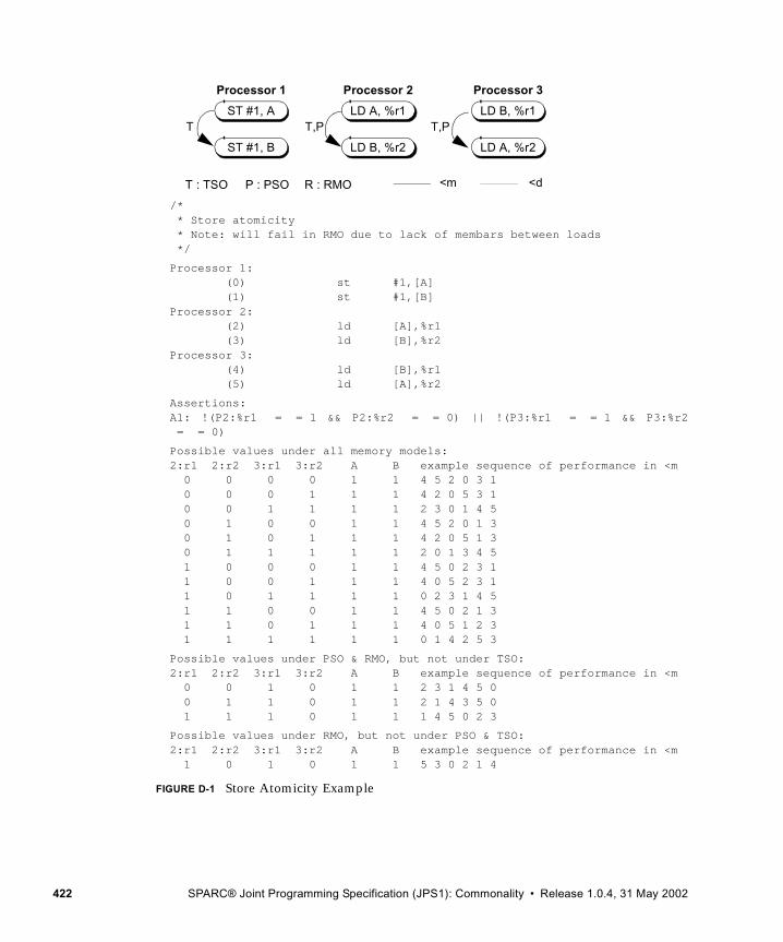
ST #1, A
ST #1, B
LD A, %r1
LD B, %r2
LD B, %r1
LD A, %r2
T T,P T,P
T : TSO P : PSO R : RMO <d<m
Processor 1 Processor 2 Processor 3
/* * Store atomicity * Note: will fail in RMO due to lack of membars between loads */
Processor 1: (0) st #1,[A] (1) st #1,[B]Processor 2: (2) ld [A],%r1 (3) ld [B],%r2Processor 3: (4) ld [B],%r1 (5) ld [A],%r2
Assertions:A1: !(P2:%r1 = = 1 && P2:%r2 = = 0) || !(P3:%r1 = = 1 && P3:%r2= = 0)
Possible values under all memory models:2:r1 2:r2 3:r1 3:r2 A B example sequence of performance in <m 0 0 0 0 1 1 4 5 2 0 3 1 0 0 0 1 1 1 4 2 0 5 3 1 0 0 1 1 1 1 2 3 0 1 4 5 0 1 0 0 1 1 4 5 2 0 1 3 0 1 0 1 1 1 4 2 0 5 1 3 0 1 1 1 1 1 2 0 1 3 4 5 1 0 0 0 1 1 4 5 0 2 3 1 1 0 0 1 1 1 4 0 5 2 3 1 1 0 1 1 1 1 0 2 3 1 4 5 1 1 0 0 1 1 4 5 0 2 1 3 1 1 0 1 1 1 4 0 5 1 2 3 1 1 1 1 1 1 0 1 4 2 5 3
Possible values under PSO & RMO, but not under TSO:2:r1 2:r2 3:r1 3:r2 A B example sequence of performance in <m 0 0 1 0 1 1 2 3 1 4 5 0 0 1 1 0 1 1 2 1 4 3 5 0 1 1 1 0 1 1 1 4 5 0 2 3
Possible values under RMO, but not under PSO & TSO:2:r1 2:r2 3:r1 3:r2 A B example sequence of performance in <m 1 0 1 0 1 1 5 3 0 2 1 4
FIGURE D-1 Store Atomicity Example
422 SPARC® Joint Programming Specification (JPS1): Commonality • Release 1.0.4, 31 May 2002
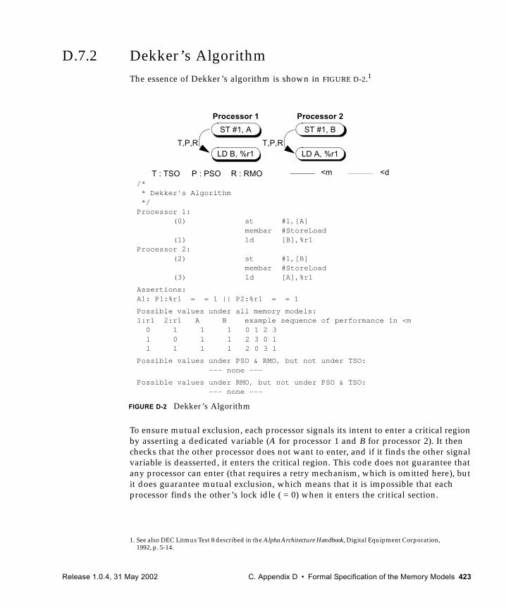
D.7.2 Dekker’s AlgorithmThe essence of Dekker’s algorithm is shown in FIGURE D-2.1
To ensure mutual exclusion, each processor signals its intent to enter a critical region by asserting a dedicated variable (A for processor 1 and B for processor 2). It then checks that the other processor does not want to enter, and if it finds the other signal variable is deasserted, it enters the critical region. This code does not guarantee that any processor can enter (that requires a retry mechanism, which is omitted here), but it does guarantee mutual exclusion, which means that it is impossible that each processor finds the other’s lock idle ( = 0) when it enters the critical section.
1. See also DEC Litmus Test 8 described in the Alpha Architecture Handbook, Digital Equipment Corporation, 1992, p. 5-14.
ST #1, A
LD B, %r1
ST #1, B
LD A, %r1T,P,R T,P,R
Processor 1 Processor 2
/* * Dekker's Algorithm */Processor 1:
(0) st #1,[A]membar #StoreLoad
(1) ld [B],%r1Processor 2:
(2) st #1,[B]membar #StoreLoad
(3) ld [A],%r1
Assertions:A1: P1:%r1 = = 1 || P2:%r1 = = 1
Possible values under all memory models:1:r1 2:r1 A B example sequence of performance in <m
0 1 1 1 0 1 2 3 1 0 1 1 2 3 0 1 1 1 1 1 2 0 3 1
Possible values under PSO & RMO, but not under TSO: --- none ---
Possible values under RMO, but not under PSO & TSO: --- none ---
T : TSO P : PSO R : RMO <d<m
FIGURE D-2 Dekker’s Algorithm
Release 1.0.4, 31 May 2002 C. Appendix D • Formal Specification of the Memory Models 423
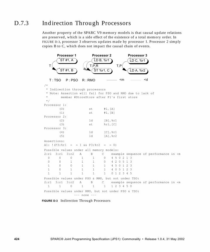
D.7.3 Indirection Through ProcessorsAnother property of the SPARC V9 memory models is that causal update relations are preserved, which is a side effect of the existence of a total memory order. In FIGURE D-3, processor 3 observes updates made by processor 1. Processor 2 simply copies B to C, which does not impact the causal chain of events.
ST #1, A
ST #1, B
LD B, %r1
ST %r1, C
LD C, %r1
LD A, %r2T T,PT,P,R
Processor 1 Processor 2 Processor 3
T : TSO P : PSO R : RMO <d<m
/* * Indirection through processors * Note: Assertion will fail for PSO and RMO due to lack of * membar #StoreStore after P1's first store */Processor 1: (0) st #1,[A] (1) st #1,[B]Processor 2: (2) ld [B],%r1 (3) st %r1,[C]Processor 3: (4) ld [C],%r1 (5) ld [A],%r2
Assertions:A1: !(P3:%r1 = = 1 && P3:%r2 = = 0)
Possible values under all memory models:2:r1 3:r1 3:r2 A B C example sequence of performance in <m 0 0 0 1 1 0 4 5 0 2 1 3 0 0 1 1 1 0 4 2 0 5 1 3 1 0 0 1 1 1 4 5 0 1 2 3 1 0 1 1 1 1 4 0 5 1 2 3 1 1 1 1 1 1 0 1 2 3 4 5
Possible values under PSO & RMO, but not under TSO:2:r1 3:r1 3:r2 A B C example sequence of performance in <m 1 1 0 1 1 1 1 2 3 4 5 0
Possible values under RMO, but not under PSO & TSO: --- none ---
FIGURE D-3 Indirection Through Processors
424 SPARC® Joint Programming Specification (JPS1): Commonality • Release 1.0.4, 31 May 2002
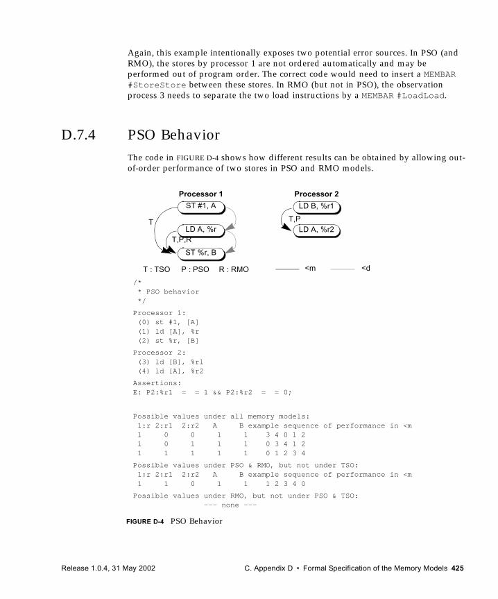
Again, this example intentionally exposes two potential error sources. In PSO (and RMO), the stores by processor 1 are not ordered automatically and may be performed out of program order. The correct code would need to insert a MEMBAR #StoreStore between these stores. In RMO (but not in PSO), the observation process 3 needs to separate the two load instructions by a MEMBAR #LoadLoad.
D.7.4 PSO BehaviorThe code in FIGURE D-4 shows how different results can be obtained by allowing out-of-order performance of two stores in PSO and RMO models.
ST #1, A
LD A, %r
LD B, %r1
LD A, %r2T,P
ST %r, B
T
T,P,R
Processor 1 Processor 2
T : TSO P : PSO R : RMO <d<m
/* * PSO behavior */
Processor 1: (0) st #1, [A] (1) ld [A], %r (2) st %r, [B]
Processor 2: (3) ld [B], %r1 (4) ld [A], %r2
Assertions:E: P2:%r1 = = 1 && P2:%r2 = = 0;
Possible values under all memory models: 1:r 2:r1 2:r2 A B example sequence of performance in <m 1 0 0 1 1 3 4 0 1 2 1 0 1 1 1 0 3 4 1 2 1 1 1 1 1 0 1 2 3 4
Possible values under PSO & RMO, but not under TSO: 1:r 2:r1 2:r2 A B example sequence of performance in <m 1 1 0 1 1 1 2 3 4 0
Possible values under RMO, but not under PSO & TSO: --- none ---
FIGURE D-4 PSO Behavior
Release 1.0.4, 31 May 2002 C. Appendix D • Formal Specification of the Memory Models 425
A store to B is allowed to be performed before a store to A. If two loads of processor 2 are performed between the two stores, then the assertion above is satisfied for the PSO and RMO models.
D.7.5 Application to CompilersA significant problem in a multiprocessor environment arises from the fact that normal compiler optimizations which reorder code can subvert programmer intent. The SPARC V9 memory model can be applied to the program rather than to an execution, to identify transformations that can be applied, provided that the program has a proper set of MEMBARs in place. In this case, the dependence order is a program-dependence order, rather than a trace-dependence order, and must include the dependences from all possible executions.
D.7.6 Verifying Memory ModelsWhile the SPARC V9 memory models were being defined, software tools were developed that automatically analyze and formally verify assembly-code sequences running in the models. The core of this collection of tools is the Murphi finite-state verifier developed by David Dill and his students at Stanford University.
For example, these tools can be used to confirm that synchronization routines operate properly in various memory models and to generate counter example traces when they fail. The tools work by exhaustively enumerating system states in a version of the memory model, so they can only be applied to fairly small assembly code examples. We found the tools to be helpful in understanding the memory models and checking our examples.1
Contact SPARC International to obtain the verification tools and a set of examples.
1. For a discussion of an earlier application of similar tools to TSO and PSO, see David Dill, Seungjoon Park, and Andreas G. Nowatzyk, “Formal Specification of Abstract Memory Models” in Research on Integrated Systems: Proceedings of the 1993 Symposium, Ed. Gaetano Borriello and Carl Ebeling, MIT Press, 1993.
426 SPARC® Joint Programming Specification (JPS1): Commonality • Release 1.0.4, 31 May 2002
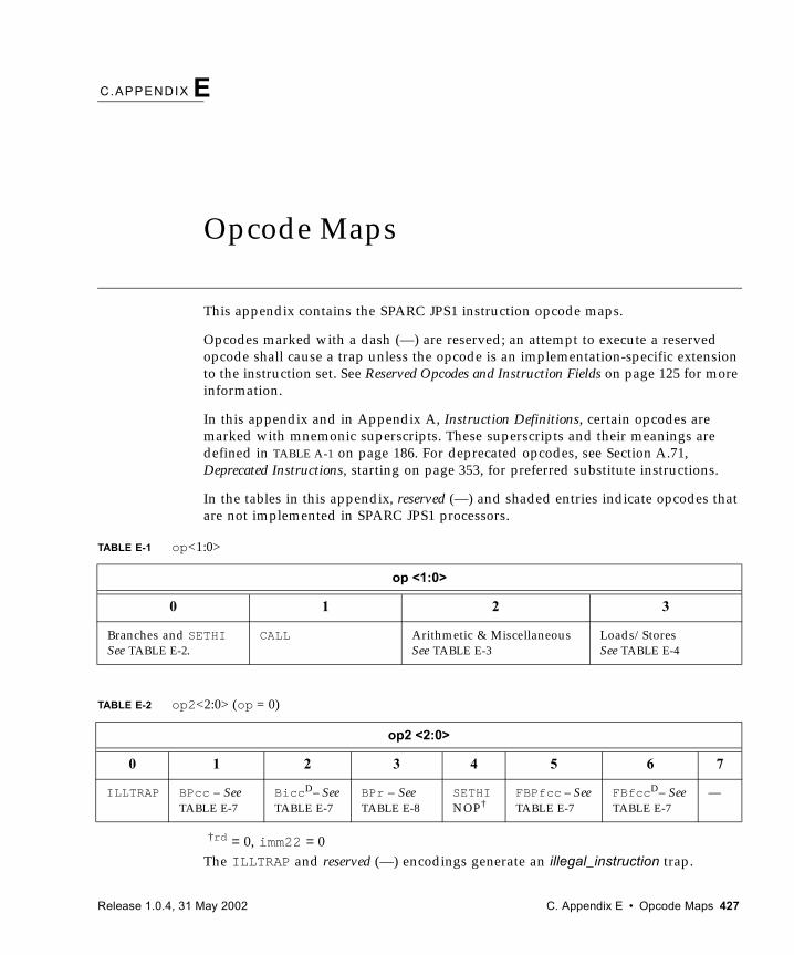
C.APPENDIX E
Opcode Maps
This appendix contains the SPARC JPS1 instruction opcode maps.
Opcodes marked with a dash (—) are reserved; an attempt to execute a reserved opcode shall cause a trap unless the opcode is an implementation-specific extension to the instruction set. See Reserved Opcodes and Instruction Fields on page 125 for more information.
In this appendix and in Appendix A, Instruction Definitions, certain opcodes are marked with mnemonic superscripts. These superscripts and their meanings are defined in TABLE A-1 on page 186. For deprecated opcodes, see Section A.71, Deprecated Instructions, starting on page 353, for preferred substitute instructions.
In the tables in this appendix, reserved (—) and shaded entries indicate opcodes that are not implemented in SPARC JPS1 processors.
†rd = 0, imm22 = 0The ILLTRAP and reserved (—) encodings generate an illegal_instruction trap.
TABLE E-1 op<1:0>
op <1:0>
0 1 2 3
Branches and SETHISee TABLE E-2.
CALL Arithmetic & MiscellaneousSee TABLE E-3
Loads/StoresSee TABLE E-4
TABLE E-2 op2<2:0> (op = 0)
op2 <2:0>
0 1 2 3 4 5 6 7
ILLTRAP BPcc – See TABLE E-7
BiccD– See TABLE E-7
BPr – See TABLE E-8
SETHINOP†
FBPfcc – See TABLE E-7
FBfccD– See TABLE E-7
—
Release 1.0.4, 31 May 2002 C. Appendix E • Opcode Maps 427
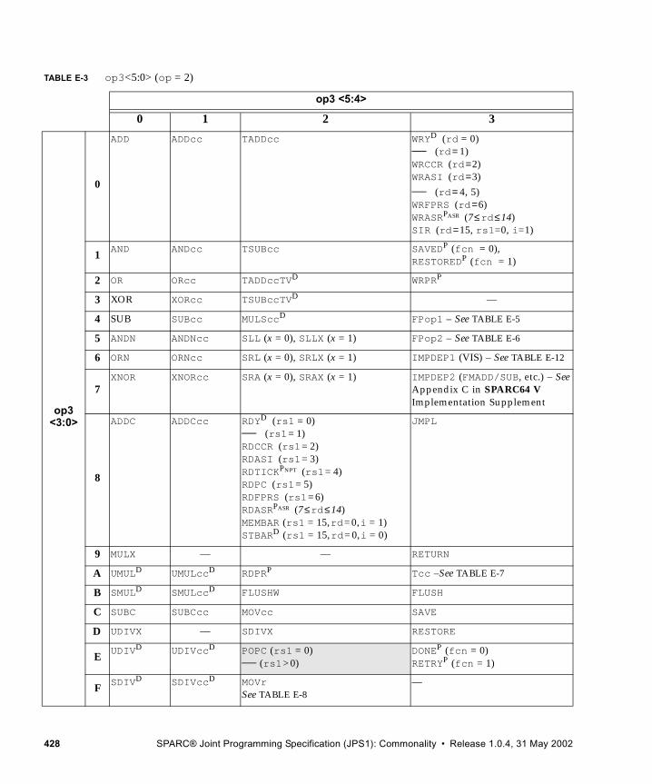
TABLE E-3 op3<5:0> (op = 2)
op3 <5:4>
0 1 2 3
op3<3:0>
0
ADD ADDcc TADDcc WRYD (rd = 0)— (rd= 1)WRCCR (rd=2)WRASI (rd=3)— (rd= 4, 5)WRFPRS (rd=6)WRASRPASR (7≤rd≤14)SIR (rd=15, rs1=0, i=1)
1AND ANDcc TSUBcc SAVEDP (fcn = 0),
RESTOREDP (fcn = 1)
2 OR ORcc TADDccTVD WRPRP
3 XOR XORcc TSUBccTVD —
4 SUB SUBcc MULSccD FPop1 – See TABLE E-5
5 ANDN ANDNcc SLL (x = 0), SLLX (x = 1) FPop2 – See TABLE E-6
6 ORN ORNcc SRL (x = 0), SRLX (x = 1) IMPDEP1 (VIS) – See TABLE E-12
7XNOR XNORcc SRA (x = 0), SRAX (x = 1) IMPDEP2 (FMADD/SUB, etc.) – See
Appendix C in SPARC64 V Implementation Supplement
8
ADDC ADDCcc RDYD (rs1 = 0)— (rs1= 1)RDCCR (rs1= 2)RDASI (rs1= 3)RDTICKPNPT (rs1= 4)RDPC (rs1= 5)RDFPRS (rs1=6)RDASRPASR (7≤rd≤14)MEMBAR (rs1 = 15,rd=0,i = 1)STBARD (rs1 = 15,rd=0,i = 0)
JMPL
9 MULX — — RETURN
A UMULD UMULccD RDPRP Tcc –See TABLE E-7
B SMULD SMULccD FLUSHW FLUSH
C SUBC SUBCcc MOVcc SAVE
D UDIVX — SDIVX RESTORE
EUDIVD UDIVccD POPC (rs1 = 0)
— (rs1>0)DONEP (fcn = 0)RETRYP (fcn = 1)
F SDIVD SDIVccD MOVrSee TABLE E-8
—
428 SPARC® Joint Programming Specification (JPS1): Commonality • Release 1.0.4, 31 May 2002
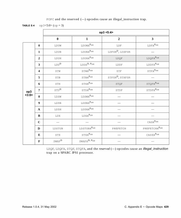
POPC and the reserved (—) opcodes cause an illegal_instruction trap.
LDQF, LDQFA, STQF, STQFA, and the reserved (—) opcodes cause an illegal_instruction trap on a SPARC JPS1 processor.
TABLE E-4 op3<5:0> (op = 3)
op3 <5:4>
0 1 2 3
op3<3:0>
0 LDUW LDUWAPASI LDF LDFAPASI
1 LDUB LDUBAPASI LDFSRD, LDXFSR —
2 LDUH LDUHAPASI LDQF LDQFAPASI
3 LDDD LDDAD, PASI LDDF LDDFAPASI
4 STW STWAPASI STF STFAPASI
5 STB STBAPASI STFSRD, STXFSR —
6 STH STHAPASI STQF STQFAPASI
7 STDD STDAPASI STDF STDFAPASI
8 LDSW LDSWAPASI — —
9 LDSB LDSBAPASI — —
A LDSH LDSHAPASI — —
B LDX LDXAPASI — —
C — — — CASAPASI
D LDSTUB LDSTUBAPASI PREFETCH PREFETCHAPASI
E STX STXAPASI — CASXAPASI
F SWAPD SWAPAD, PASI — —
Release 1.0.4, 31 May 2002 C. Appendix E • Opcode Maps 429
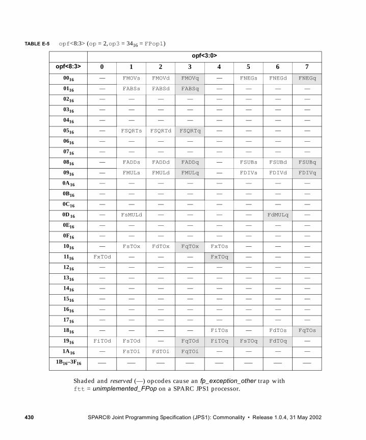
Shaded and reserved (—) opcodes cause an fp_exception_other trap with ftt = unimplemented_FPop on a SPARC JPS1 processor.
TABLE E-5 opf<8:3> (op = 2,op3 = 3416 = FPop1)
opf<3:0>
opf<8:3> 0 1 2 3 4 5 6 7
0016 — FMOVs FMOVd FMOVq — FNEGs FNEGd FNEGq
0116 — FABSs FABSd FABSq — — — —
0216 — — — — — — — —
0316 — — — — — — — —
0416 — — — — — — — —
0516 — FSQRTs FSQRTd FSQRTq — — — —
0616 — — — — — — — —
0716 — — — — — — — —
0816 — FADDs FADDd FADDq — FSUBs FSUBd FSUBq
0916 — FMULs FMULd FMULq — FDIVs FDIVd FDIVq
0A16 — — — — — — — —
0B16 — — — — — — — —
0C16 — — — — — — — —
0D16 — FsMULd — — — — FdMULq —
0E16 — — — — — — — —
0F16 — — — — — — — —
1016 — FsTOx FdTOx FqTOx FxTOs — — —
1116 FxTOd — — — FxTOq — — —
1216 — — — — — — — —
1316 — — — — — — — —
1416 — — — — — — — —
1516 — — — — — — — —
1616 — — — — — — — —
1716 — — — — — — — —
1816 — — — — FiTOs — FdTOs FqTOs
1916 FiTOd FsTOd — FqTOd FiTOq FsTOq FdTOq —
1A16 — FsTOi FdTOi FqTOi — — — —
1B16–3F16 — — — — — — — —
430 SPARC® Joint Programming Specification (JPS1): Commonality • Release 1.0.4, 31 May 2002
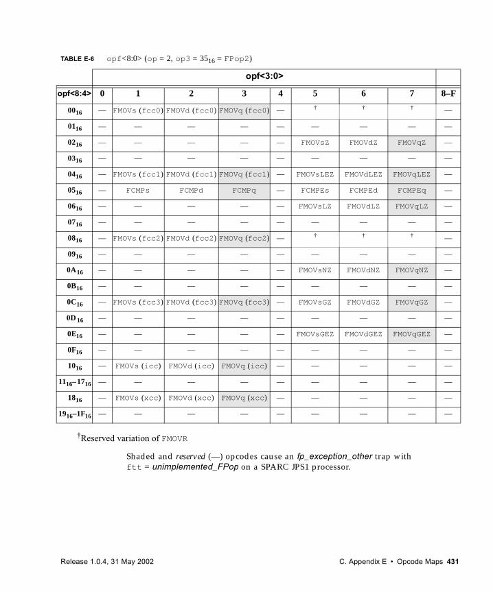
†Reserved variation of FMOVR
Shaded and reserved (—) opcodes cause an fp_exception_other trap with ftt = unimplemented_FPop on a SPARC JPS1 processor.
TABLE E-6 opf<8:0> (op = 2, op3 = 3516 = FPop2)
opf<3:0>
opf<8:4> 0 1 2 3 4 5 6 7 8–F
0016 — FMOVs (fcc0) FMOVd (fcc0) FMOVq (fcc0) — † † † —
0116 — — — — — — — — —
0216 — — — — — FMOVsZ FMOVdZ FMOVqZ —
0316 — — — — — — — — —
0416 — FMOVs (fcc1) FMOVd (fcc1) FMOVq (fcc1) — FMOVsLEZ FMOVdLEZ FMOVqLEZ —
0516 — FCMPs FCMPd FCMPq — FCMPEs FCMPEd FCMPEq —
0616 — — — — — FMOVsLZ FMOVdLZ FMOVqLZ —
0716 — — — — — — — — —
0816 — FMOVs (fcc2) FMOVd (fcc2) FMOVq (fcc2) — † † † —
0916 — — — — — — — — —
0A16 — — — — — FMOVsNZ FMOVdNZ FMOVqNZ —
0B16 — — — — — — — — —
0C16 — FMOVs (fcc3) FMOVd (fcc3) FMOVq (fcc3) — FMOVsGZ FMOVdGZ FMOVqGZ —
0D16 — — — — — — — — —
0E16 — — — — — FMOVsGEZ FMOVdGEZ FMOVqGEZ —
0F16 — — — — — — — — —
1016 — FMOVs (icc) FMOVd (icc) FMOVq (icc) — — — — —
1116–1716 — — — — — — — — —
1816 — FMOVs (xcc) FMOVd (xcc) FMOVq (xcc) — — — — —
1916–1F16 — — — — — — — — —
Release 1.0.4, 31 May 2002 C. Appendix E • Opcode Maps 431
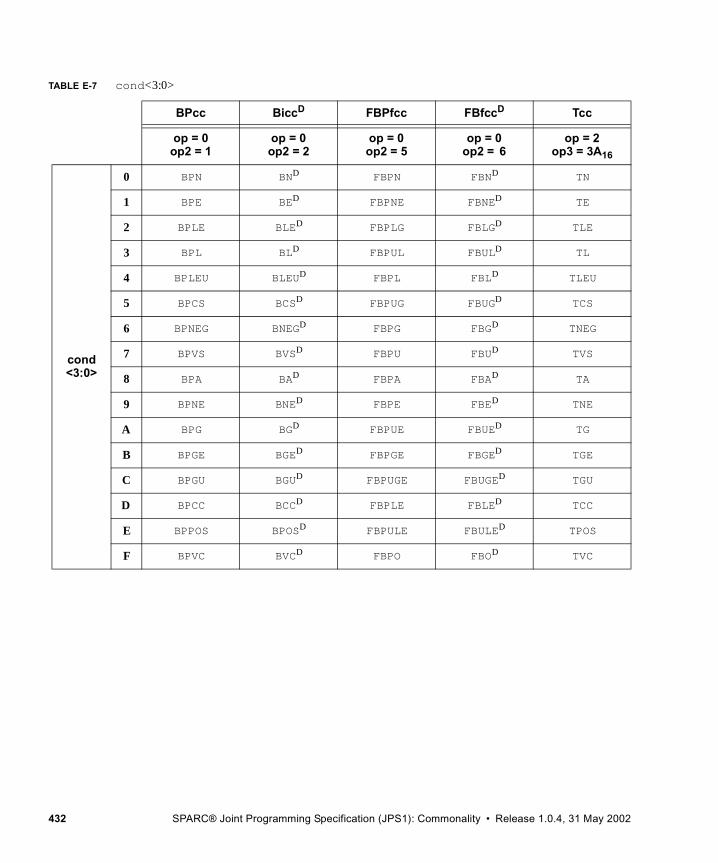
TABLE E-7 cond<3:0>
BPcc BiccD FBPfcc FBfccD Tcc
op = 0op2 = 1
op = 0op2 = 2
op = 0op2 = 5
op = 0op2 = 6
op = 2op3 = 3A16
cond<3:0>
0 BPN BND FBPN FBND TN
1 BPE BED FBPNE FBNED TE
2 BPLE BLED FBPLG FBLGD TLE
3 BPL BLD FBPUL FBULD TL
4 BPLEU BLEUD FBPL FBLD TLEU
5 BPCS BCSD FBPUG FBUGD TCS
6 BPNEG BNEGD FBPG FBGD TNEG
7 BPVS BVSD FBPU FBUD TVS
8 BPA BAD FBPA FBAD TA
9 BPNE BNED FBPE FBED TNE
A BPG BGD FBPUE FBUED TG
B BPGE BGED FBPGE FBGED TGE
C BPGU BGUD FBPUGE FBUGED TGU
D BPCC BCCD FBPLE FBLED TCC
E BPPOS BPOSD FBPULE FBULED TPOS
F BPVC BVCD FBPO FBOD TVC
432 SPARC® Joint Programming Specification (JPS1): Commonality • Release 1.0.4, 31 May 2002
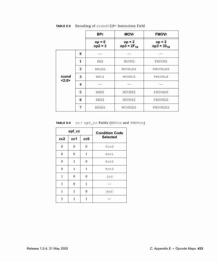
TABLE E-8 Encoding of rcond<2:0> Instruction Field
BPr MOVr FMOVr
op = 0op2 = 3
op = 2op3 = 2F16
op = 2op3 = 3516
rcond<2:0>
0 — — —
1 BRZ MOVRZ FMOVRZ
2 BRLEZ MOVRLEZ FMOVRLEZ
3 BRLZ MOVRLZ FMOVRLZ
4 — — —
5 BRNZ MOVRNZ FMOVRNZ
6 BRGZ MOVRGZ FMOVRGZ
7 BRGEZ MOVRGEZ FMOVRGEZ
TABLE E-9 cc / opf_cc Fields (MOVcc and FMOVcc)
opf_cc Condition CodeSelectedcc2 cc1 cc0
0 0 0 fcc0
0 0 1 fcc1
0 1 0 fcc2
0 1 1 fcc3
1 0 0 icc
1 0 1 —
1 1 0 xcc
1 1 1 —
Release 1.0.4, 31 May 2002 C. Appendix E • Opcode Maps 433
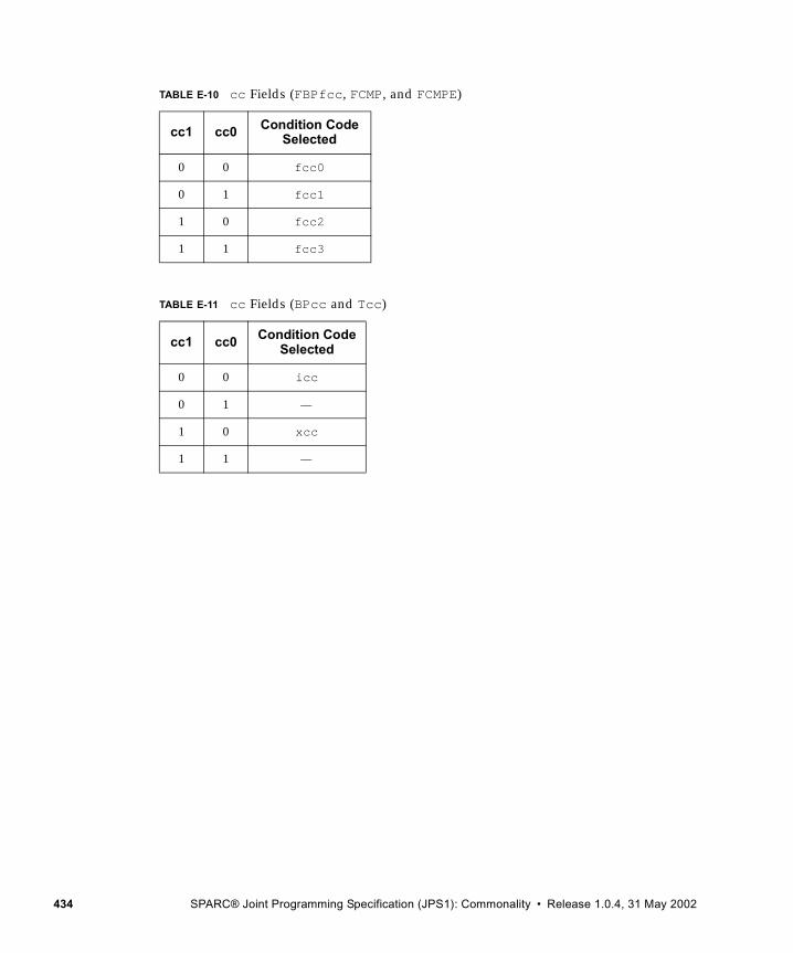
TABLE E-10 cc Fields (FBPfcc, FCMP, and FCMPE)
cc1 cc0 Condition CodeSelected
0 0 fcc0
0 1 fcc1
1 0 fcc2
1 1 fcc3
TABLE E-11 cc Fields (BPcc and Tcc)
cc1 cc0 Condition CodeSelected
0 0 icc
0 1 —
1 0 xcc
1 1 —
434 SPARC® Joint Programming Specification (JPS1): Commonality • Release 1.0.4, 31 May 2002
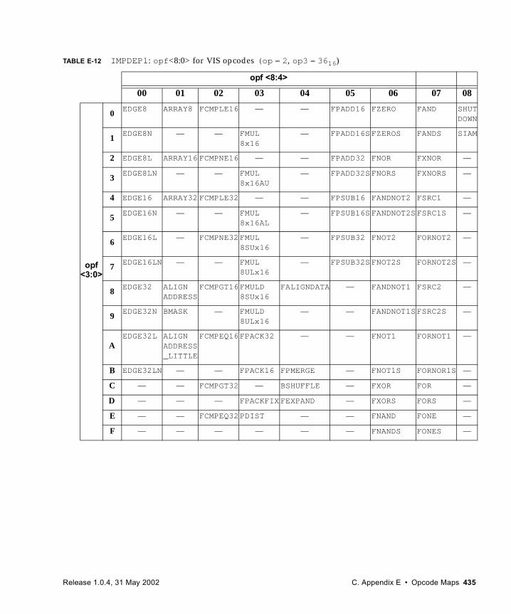
TABLE E-12 IMPDEP1: opf<8:0> for VIS opcodes (op = 2, op3 = 3616)
opf <8:4>
00 01 02 03 04 05 06 07 08
opf<3:0>
0 EDGE8 ARRAY8 FCMPLE16 — — FPADD16 FZERO FAND SHUTDOWN
1 EDGE8N — — FMUL8x16
— FPADD16S FZEROS FANDS SIAM
2 EDGE8L ARRAY16 FCMPNE16 — — FPADD32 FNOR FXNOR —
3 EDGE8LN — — FMUL8x16AU
— FPADD32S FNORS FXNORS —
4 EDGE16 ARRAY32 FCMPLE32 — — FPSUB16 FANDNOT2 FSRC1 —
5 EDGE16N — — FMUL8x16AL
— FPSUB16S FANDNOT2SFSRC1S —
6EDGE16L — FCMPNE32 FMUL
8SUx16— FPSUB32 FNOT2 FORNOT2 —
7 EDGE16LN — — FMUL8ULx16
— FPSUB32S FNOT2S FORNOT2S —
8 EDGE32 ALIGNADDRESS
FCMPGT16 FMULD8SUx16
FALIGNDATA — FANDNOT1 FSRC2 —
9EDGE32N BMASK — FMULD
8ULx16— — FANDNOT1SFSRC2S —
AEDGE32L ALIGN
ADDRESS_LITTLE
FCMPEQ16 FPACK32 — — FNOT1 FORNOT1 —
B EDGE32LN — — FPACK16 FPMERGE — FNOT1S FORNOR1S —
C — — FCMPGT32 — BSHUFFLE — FXOR FOR —
D — — — FPACKFIX FEXPAND — FXORS FORS —
E — — FCMPEQ32 PDIST — — FNAND FONE —
F — — — — — — FNANDS FONES —
Release 1.0.4, 31 May 2002 C. Appendix E • Opcode Maps 435

436 SPARC® Joint Programming Specification (JPS1): Commonality • Release 1.0.4, 31 May 2002
C.APPENDIX F
Memory Management Unit
The Memory Management Unit (MMU) conforms to the requirements set forth in the SPARC V9 Architecture Manual. In particular, it supports a 64-bit virtual address space, software TLB-miss processing only (no hardware page table walk), simplified protection encoding, and multiple page sizes.
This chapter describes the Memory Management Unit, as seen by the operating system software, in these sections:
■ Virtual Address Translation on page 437■ Translation Table Entry (TTE) on page 440■ Translation Storage Buffer on page 443■ Hardware Support for TSB Access on page 445■ Faults and Traps on page 449■ MMU Operation Summary on page 451■ ASI Value, Context, and Endianness Selection for Translation on page 453■ Reset, Disable, and RED_state Behavior on page 455■ SPARC V9 “MMU Requirements” Annex on page 457■ Internal Registers and ASI Operations on page 457■ MMU Bypass on page 472■ Translation Lookaside Buffer Hardware on page 473
F.1 Virtual Address TranslationThe MMUs support four page sizes: 8 Kbytes, 64 Kbytes, 512 Kbytes, and 4 Mbytes. Separate Instruction and Data MMUs (IMMU and DMMU, respectively) are provided to enable concurrent virtual-to-physical address translations for instruction and data. A 64-bit virtual address (VA) space is supported, with a minimum of 43 bits of physical address (PA). In each translation, the virtual page number is replaced by a physical page number, which is concatenated with the page offset to form the full physical address, as illustrated in FIGURE F-1.
Release 1.0.4, 31 May 2002 C. Appendix F • Memory Management Unit 437
Each MMU consists of one or more Translation Lookaside Buffers (TLBs), including micro-TLB structures. The organization of TLB structures may be different between the Instruction MMU and the Data MMU.
FIGURE F-1 Virtual-to-Physical Address Translation for All Four Page Sizes
The operating system maintains translation information in an arbitrary data structure, called the software translation table in this appendix. The I- and D-MMU TLBs act as independent caches of the software translation table, providing appropriate concurrency for virtual-to-physical address translation.
IMPL. DEP. #222: TLB organization is JPS1 implementation dependent.
0
0
12
1213
1363
42
8-Kbyte Virtual Page Number
8-Kbyte Physical Page Number
Page Offset
Page Offset
0
0
15
1516
1663
42
64-Kbyte Virtual Page Number
64-Kbyte Physical Page Number
Page Offset
Page Offset
0
0
18
1819
1963
42
512-Kbyte Virtual Page Number
512-Kbyte PPN
Page Offset
Page Offset
VA
PA
PA
PA
VA
VA
8 Kbyte
64 Kbyte
512 Kbyte
0
0
21
2122
2263
42
4-Mbyte Virtual Page Number
4-Mbyte PPN
Page Offset
Page Offset PA
VA
4 Mbyte
MMU
MMU
MMU
MMU
438 SPARC® Joint Programming Specification (JPS1): Commonality • Release 1.0.4, 31 May 2002
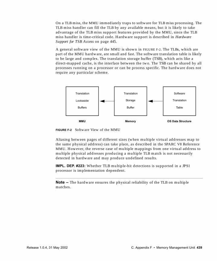
On a TLB miss, the MMU immediately traps to software for TLB miss processing. The TLB miss handler can fill the TLB by any available means, but it is likely to take advantage of the TLB miss support features provided by the MMU, since the TLB miss handler is time-critical code. Hardware support is described in Hardware Support for TSB Access on page 445.
A general software view of the MMU is shown in FIGURE F-2. The TLBs, which are part of the MMU hardware, are small and fast. The software translation table is likely to be large and complex. The translation storage buffer (TSB), which acts like a direct-mapped cache, is the interface between the two. The TSB can be shared by all processes running on a processor or can be process specific. The hardware does not require any particular scheme.
FIGURE F-2 Software View of the MMU
Aliasing between pages of different sizes (when multiple virtual addresses map to the same physical address) can take place, as described in the SPARC V8 Reference MMU. However, the reverse case of multiple mappings from one virtual address to multiple physical addresses producing a multiple TLB match is not necessarily detected in hardware and may produce undefined results.
IMPL. DEP. #223: Whether TLB multiple-hit detections is supported in a JPS1 processor is implementation dependent.
Note – The hardware ensures the physical reliability of the TLB on multiple matches.
Translation
Lookaside
Buffers
Translation
Buffer
Software
Translation
Table
MMU Memory OS Data Structure
Storage
Release 1.0.4, 31 May 2002 C. Appendix F • Memory Management Unit 439
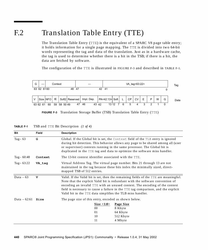
F.2 Translation Table Entry (TTE)The Translation Table Entry (TTE) is the equivalent of a SPARC V8 page table entry; it holds information for a single page mapping. The TTE is divided into two 64-bit words representing the tag and data of the translation. Just as in a hardware cache, the tag is used to determine whether there is a hit in the TSB; if there is a hit, the data are fetched by software.
The configuration of the TTE is illustrated in FIGURE F-3 and described in TABLE F-1.
FIGURE F-3 Translation Storage Buffer (TSB) Translation Table Entry (TTE)
TABLE F-1 TSB and TTE Bit Description (1 of 4)
Bit Field Description
Tag– 63 G Global. If the Global bit is set, the Context field of the TLB entry is ignored during hit detection. This behavior allows any page to be shared among all (user or supervisor) contexts running in the same processor. The Global bit is duplicated in the TTE tag and data to optimize the software miss handler.
Tag– 60:48 Context The 13-bit context identifier associated with the TTE.
Tag– 63:22 VA_tag Virtual Address Tag. The virtual page number. Bits 21 through 13 are not maintained in the tag because these bits index the minimally sized, direct-mapped TSB of 512 entries.
Data – 63 V Valid. If the Valid bit is set, then the remaining fields of the TTE are meaningful. Note that the explicit Valid bit is redundant with the software convention of encoding an invalid TTE with an unused context. The encoding of the context field is necessary to cause a failure in the TTE tag comparison, and the explicit Valid bit in the TTE data simplifies the TLB miss handler.
Data – 62:61 Size The page size of this entry, encoded as shown below.Size <1:0> Page Size00 8 Kbyte01 64 Kbyte10 512 Kbyte11 4 Mbyte
DataPA<42:13>Size Soft
011363
CVCP
2312
WP
461 6062 5
GV E
6
L
7
Soft2
5059
NFO
49 43
IE
58
Reserved
4247 46
Impl. Dep.
G VA_tag<63:22>Context
063Tag
414247
—
62 6061
—
48
440 SPARC® Joint Programming Specification (JPS1): Commonality • Release 1.0.4, 31 May 2002
Data – 60 NFO No Fault Only. If the no-fault-only bit is set, loads with ASI_PRIMARY_NO_FAULT, ASI_SECONDARY_NO_FAULT, and their *_LITTLE variations are translated. Any other access will trap with a data_access_exception trap (FT = 1016). The NFO bit in the IMMU is read as 0 and ignored when written. The ITLB-miss handler should generate an error if this bit is set before the TTE is loaded into the TLB.
Data – 59 IE Invert Endianness. If this bit is set for a page, accesses to the page are processed with inverse endianness from that specified by the instruction (big for little, little for big). See page 453 for details. The IE bit in the IMMU is read as 0 and ignored when written. Note: This bit is intended to be set primarily for noncacheable accesses. The performance of cacheable accesses will be degraded as if the access missed the D-cache.
Data - 58:50 Soft2 Software-defined field, provided for use by the operating system. The Soft2 field can be written with any value in the TSB. Hardware is not required to maintain this field in the TLB, so when it is read from the TLB, it may read as zero.
Data – 49:47 Reserved Reserved, read as 0.
Data – 46:43 Implementation dependent
This field is implementation dependent (see impl. dep. #224 below); see each Implementation Supplement for details regarding usage of this field.
Data – 42:13 PA The physical page number. Page offset bits for larger page sizes (PA<15:13>, PA<18:13>, and PA<21:13> for 64-Kbyte, 512-Kbyte, and 4-Mbyte pages, respectively) are ignored during normal translation.
IMPL. DEP. #224: Physical address width support by the MMU is implementation dependent in JPS1; minimum PA width is 43 bits.
IMPL. DEP. #238: When page offset bits for larger page sizes (PA<15:13>, PA<18:13>, and PA<21:13> for 64-Kbyte, 512-Kbyte, and 4-Mbyte pages, respectively) are stored in the TLB, it is implementation dependent whether the data returned from those fields by a Data Access read are zero or the data previously written to them.
Data – 12:7 Soft Software-defined field, provided for use by the operating system. The Soft field can be written with any value in the TSB. Hardware is not required to maintain this field in the TLB, so when it is read from the TLB, it may read as zero.
TABLE F-1 TSB and TTE Bit Description (2 of 4)
Bit Field Description
Release 1.0.4, 31 May 2002 C. Appendix F • Memory Management Unit 441
Data – 6 L If the lock bit is set, then the TTE entry will be “locked down” when it is loaded into the TLB; that is, if this entry is valid, it will not be replaced by the automatic replacement algorithm invoked by an ASI store to the Data In Register. The lock bit has no meaning for an invalid entry. While a minimum of 14 entries shall be lockable by software in the TLB structure, software must ensure that at least one entry is not locked when replacing a TLB entry.
IMPL. DEP. #225: The mechanism by which entries in TLB are locked is implementation dependent in JPS1.
IMPL. DEP. #242: An implementation containing multiple TLBs may implement the L (lock) bit in all TLBs but is only required to implement a lock bit in one TLB for each page size. If the lock bit is not implemented in a particular TLB, it reads as 0 and writes to it are ignored.
Data – 5Data – 4
CP,CV
The cacheable-in-physically-indexed-cache bit and cacheable-in-virtually-indexed-cache bit determine the placement of data in the caches. Given an implementation with a physically indexed instruction cache, a virtually indexed data cache, and a physically indexed unified second-level cache, the following table illustrates how the CP and CV bits could be used.
The MMU does not operate on the cacheable bits but merely passes them through to the cache subsystem. The CV bit in the IMMU is read as zero and ignored when written.
IMPL. DEP. #226: Whether the CV bit is supported in TTE is implementation dependent in JPS1. When the CV bit in TTE is not provided and the implementation has virtually indexed caches, the implementation should support hardware unaliasing for the caches.
Data – 3 E Side effect. If the side-effect bit is set, nonfaulting loads will trap for addresses within the page, noncacheable memory accesses other than block loads and stores are strongly ordered against other E-bit accesses, and noncacheable stores are not merged. This bit should be set for pages that map I/O devices having side effects. Note, however, that the E bit does not prevent normal instruction prefetching. The E bit in the IMMU is read as 0 and ignored when written.Note: The E bit does not force a noncacheable access. It is expected, but not required, that the CP and CV bits will be set to 0 when the E bit is set. If both the CP and CV bits are set to 1 along with the E bit, the result is undefined.Note Also: The E bit and the NFO bit are mutually exclusive; both bits should never be set in any TTE.
TABLE F-1 TSB and TTE Bit Description (3 of 4)
Bit Field Description
Cacheable(CP, CV)
Meaning of TTE when placed in:
I-TLB (Instruction Cache PA-indexed) D-TLB (Data Cache VA-indexed)
00, 01 Noncacheable Noncacheable
10 Cacheable E-cache, I-cache Cacheable E-cache
11 Cacheable E-cache, I-cache Cacheable E-cache, D-cache
442 SPARC® Joint Programming Specification (JPS1): Commonality • Release 1.0.4, 31 May 2002
Compatibility Note – Referenced and Modified bits are maintained by software. The Global, Privileged, and Writable fields replace the 3-bit ACC field of the SPARC V8 Reference MMU Page Translation Entry.
F.3 Translation Storage BufferThe Translation Storage Buffer (TSB) is an array of Translation Table Entries managed entirely by software. It serves as a cache of the software translation table, used to quickly reload the TLB in the event of a TLB miss. The discussion in this section assumes the use of the hardware support for TSB access described in Hardware Support for TSB Access on page 445, although the operating system is not required to make use of this support hardware.
Inclusion of the TLB entries in the TSB is not required; that is, translation information that is not present in the TSB can exist in the TLB.
A bit in the TSB register allows the TSB 64-Kbyte pointer to be computed for the case of common or split 8-Kbyte/64-Kbyte TSBs.
F.3.1 TSB Indexing SupportNo hardware TSB indexing support is provided for the 512-Kbyte and 4-Mbyte page TTEs. However, since the TSB is entirely software managed, the operating system may choose to place these larger page TTEs in the TSB by forming the appropriate
Data – 2 P Privileged. If the P bit is set, only the supervisor can access the page mapped by the TTE. If the P bit is set and an access to the page is attempted when PSTATE.PRIV=0, then the MMU signals an instruction_access_exception or data_access_exception trap (FT = 116).
Data – 1 W Writable. If the W bit is set, the page mapped by this TTE has write permission granted. Otherwise, write permission is not granted, and the MMU causes a fast_data_access_protection trap if a write is attempted. The W bit in the IMMU is read as 0 and ignored when written.
Data – 0 G Global. This bit must be identical to the Global bit in the TTE tag. Like the Valid bit, the Global bit in the TTE tag is necessary for the TSB hit comparison, and the Global bit in the TTE data facilitates the loading of a TLB entry.
TABLE F-1 TSB and TTE Bit Description (4 of 4)
Bit Field Description
Release 1.0.4, 31 May 2002 C. Appendix F • Memory Management Unit 443
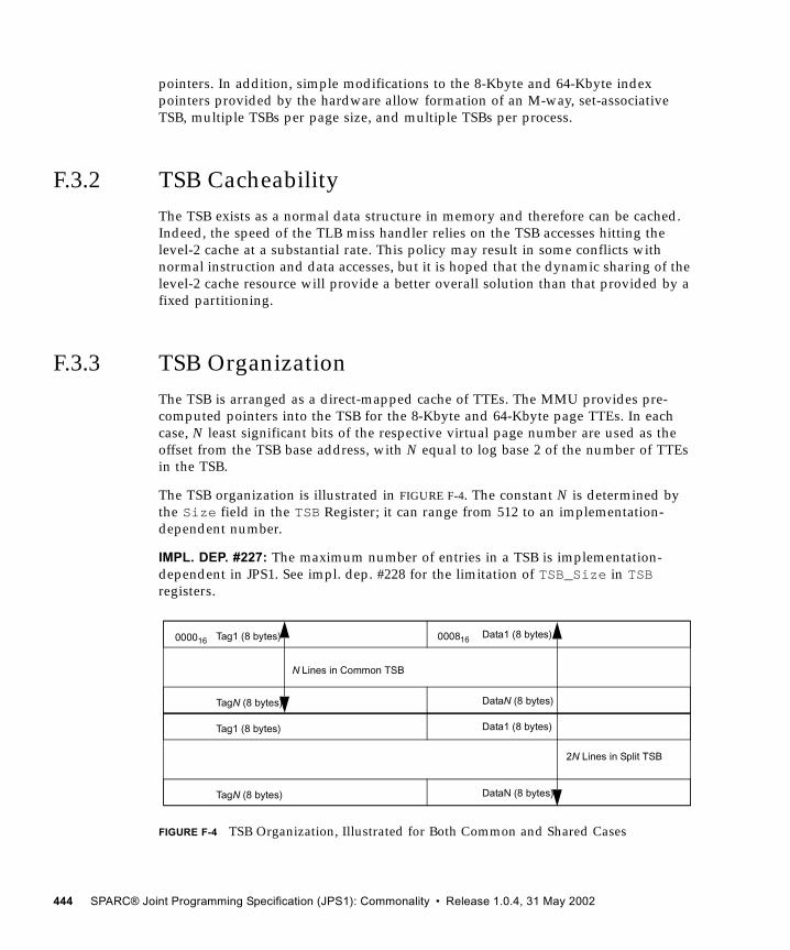
pointers. In addition, simple modifications to the 8-Kbyte and 64-Kbyte index pointers provided by the hardware allow formation of an M-way, set-associative TSB, multiple TSBs per page size, and multiple TSBs per process.
F.3.2 TSB CacheabilityThe TSB exists as a normal data structure in memory and therefore can be cached. Indeed, the speed of the TLB miss handler relies on the TSB accesses hitting the level-2 cache at a substantial rate. This policy may result in some conflicts with normal instruction and data accesses, but it is hoped that the dynamic sharing of the level-2 cache resource will provide a better overall solution than that provided by a fixed partitioning.
F.3.3 TSB OrganizationThe TSB is arranged as a direct-mapped cache of TTEs. The MMU provides pre-computed pointers into the TSB for the 8-Kbyte and 64-Kbyte page TTEs. In each case, N least significant bits of the respective virtual page number are used as the offset from the TSB base address, with N equal to log base 2 of the number of TTEs in the TSB.
The TSB organization is illustrated in FIGURE F-4. The constant N is determined by the Size field in the TSB Register; it can range from 512 to an implementation-dependent number.
IMPL. DEP. #227: The maximum number of entries in a TSB is implementation-dependent in JPS1. See impl. dep. #228 for the limitation of TSB_Size in TSB registers.
FIGURE F-4 TSB Organization, Illustrated for Both Common and Shared Cases
Tag1 (8 bytes) Data1 (8 bytes)000016 000816
TagN (8 bytes) DataN (8 bytes)
N Lines in Common TSB
Tag1 (8 bytes) Data1 (8 bytes)
TagN (8 bytes) DataN (8 bytes)
2N Lines in Split TSB
444 SPARC® Joint Programming Specification (JPS1): Commonality • Release 1.0.4, 31 May 2002
F.4 Hardware Support for TSB AccessThe MMU hardware provides services to allow the TLB-miss handler to efficiently reload a missing TLB entry for an 8-Kbyte or 64-Kbyte page. These services include:
■ Formation of TSB Pointers, based on the missing virtual address and address space identifier
■ Formation of the TTE Tag Target used for the TSB tag comparison
■ Efficient atomic write of a TLB entry with a single store ASI operation
■ Alternate globals on MMU-signalled traps
F.4.1 Typical TLB Miss/Refill SequenceA typical TLB miss-and-refill sequence is the following:
1. A TLB miss causes either a fast_instruction_access_MMU_miss or a fast_data_access_MMU_miss exception.
2. The appropriate TLB miss handler reads the TSB Pointers and the TTE Tag Target, using ASI loads.
3. Using this information, the TLB miss handler checks to see if the desired TTE exists in the TSB. If so, the TTE data are loaded into the TLB Data In Register to initiate an atomic write of the TLB entry chosen by the replacement algorithm.
4. If the TTE does not exist in the TSB, then the TLB miss handler jumps to the more sophisticated, and slower, TSB miss handler.
The virtual address used in the formation of the pointer addresses comes from the Tag Access Register, which holds the virtual address and context of the load or store responsible for the MMU exception. See Translation Table Entry (TTE) on page 440.
Note – There are no separate physical registers in hardware for the pointer registers; rather, they are implemented through a dynamic reordering of the data stored in the Tag Access and the TSB registers.
F.4.2 TSB Pointer FormationHardware provides pointers for the most common cases of 8-Kbyte and 64-Kbyte page miss processing. These pointers give the virtual addresses where the 8-Kbyte and 64-Kbyte TTEs are stored if either are present in the TSB.
Release 1.0.4, 31 May 2002 C. Appendix F • Memory Management Unit 445
Input Values for TSB Pointer Formation
The pointer to the TTE in the TSB is generated from the following parameters as inputs:
■ TSB base address (TSB_Base)■ Virtual address (VA)■ TSB_size■ TSB_split■ TSB_Hash
The TSB base address is in either of I/D Primary/Secondary (provided only for data)/Nucleus TSB Extension Registers. Depending on the context that generated the TLB miss, an appropriate TSB Extension Register is selected (which may be combined with the TSB_Base field from the TSB Base Register; see Note below). Note that the context with the TLB miss is logged in I/D Synchronous Fault Status Register.
TSB_size and TSB_split are supplied also from the selected TSB Extension Register.
The virtual page number to be used for TSB pointer formation is in I/D Tag Access Register.
TSB_Hash is a representation of the context that generated a TLB miss. Depending on the implementation, the source of the TSB_Hash may vary. For details, refer to the appropriate Implementation Supplements.
IMPL. DEP. #228: Whether TSB_Hash is supplied from a TSB Extension Register or from a context-ID register is implementation dependent in JPS1. Only for cases of direct hash with context-ID can the width of the TSB_size field be wider than 3 bits.
Note – TSB_Base address may be generated by exclusive-ORing TSB_Base register and TSB Extension Register contents, for compatibility with UltraSPARC I/II TSB pointer formation. In this case, if the TSB Extension Registers hold 0 as TSB_Base, the value in TSB_Base register becomes the TSB_Base address, thereby maintaining compatibility with UltraSPARC I/II TLB miss handling software. In addition, TSB_Base may be taken directly from an appropriate TSB Extension Register. In that case, the implementation should provide the way to maintain compatibility with UltraSPARC I/II TLB miss handler software.
IMPL. DEP. #229: Whether the implementation generates the TSB_Base address by exclusive-ORing the TSB_Base register and a TSB Extension Register or by taking TSB_Base field directly from the TSB Extension Register is implementation dependent in JPS1. This implementation dependency is only to maintain compatibility with the TLB miss handling software of UltraSPARC I/II.
446 SPARC® Joint Programming Specification (JPS1): Commonality • Release 1.0.4, 31 May 2002
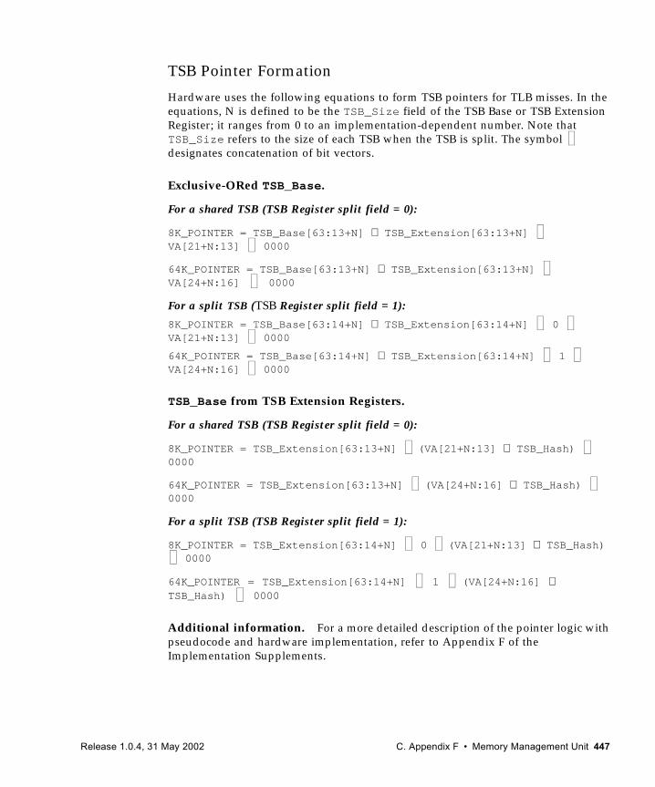
TSB Pointer Formation
Hardware uses the following equations to form TSB pointers for TLB misses. In the equations, N is defined to be the TSB_Size field of the TSB Base or TSB Extension Register; it ranges from 0 to an implementation-dependent number. Note that TSB_Size refers to the size of each TSB when the TSB is split. The symbol designates concatenation of bit vectors.
Exclusive-ORed TSB_Base.
For a shared TSB (TSB Register split field = 0):
8K_POINTER = TSB_Base[63:13+N] ⊕ TSB_Extension[63:13+N] VA[21+N:13] 0000
64K_POINTER = TSB_Base[63:13+N] ⊕ TSB_Extension[63:13+N] VA[24+N:16] 0000
For a split TSB (TSB Register split field = 1):
8K_POINTER = TSB_Base[63:14+N] ⊕ TSB_Extension[63:14+N] 0 VA[21+N:13] 0000
64K_POINTER = TSB_Base[63:14+N] ⊕ TSB_Extension[63:14+N] 1 VA[24+N:16] 0000
TSB_Base from TSB Extension Registers.
For a shared TSB (TSB Register split field = 0):
8K_POINTER = TSB_Extension[63:13+N] (VA[21+N:13] ⊕ TSB_Hash) 0000
64K_POINTER = TSB_Extension[63:13+N] (VA[24+N:16] ⊕ TSB_Hash) 0000
For a split TSB (TSB Register split field = 1):
8K_POINTER = TSB_Extension[63:14+N] 0 (VA[21+N:13] ⊕ TSB_Hash) 0000
64K_POINTER = TSB_Extension[63:14+N] 1 (VA[24+N:16] ⊕ TSB_Hash) 0000
Additional information. For a more detailed description of the pointer logic with pseudocode and hardware implementation, refer to Appendix F of the Implementation Supplements.
Release 1.0.4, 31 May 2002 C. Appendix F • Memory Management Unit 447
The TSB Tag Target (described on page 464) is formed by alignment of the missing access VA (from the Tag Access Register) and the current context to positions found above in the description of the TTE tag, allowing a simple XOR instruction for TSB hit detection.
F.4.3 Required TLB ConditionsThe following items must be locked in the TLB to avoid an error condition: TLB miss handler and data, TSB and linked data, asynchronous trap handlers and data.
F.4.4 Required TSB ConditionsThe following items must be locked in the TSB (not necessarily the TLB) to avoid an error condition: TSB miss handler and data, interrupt-vector handler and data.
F.4.5 MMU Global Registers SelectionIn the SPARC V9 normal trap model, the software is presented with an alternate set of global registers in the Integer Register file. A JPS1 processor provides an additional feature to facilitate fast handling of TLB misses. For the following traps, the trap handler is presented with a special set of MMU globals:■ fast_instruction_access_MMU_miss■ fast_data_access_MMU_miss■ instruction_access_exception■ data_access_exception■ fast_data_access_protection
Trap handlers for the privileged_action, mem_address_not_aligned, and *_mem_address_not_aligned traps use the standard alternate global registers.
Compatibility Note – The MMU does not perform hardware tablewalking. JPS1 MMU hardware never directly reads or writes the TSB.
448 SPARC® Joint Programming Specification (JPS1): Commonality • Release 1.0.4, 31 May 2002
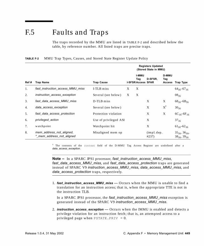
F.5 Faults and TrapsThe traps recorded by the MMU are listed in TABLE F-2 and described below the table, by reference number. All listed traps are precise traps.
† The contents of the context field of the D-MMU Tag Access Register are undefined after adata_access_exception.
Note – In a SPARC JPS1 processor, fast_instruction_access_MMU_miss, fast_data_access_MMU_miss, and fast_data_access_protection traps are generated instead of SPARC V9 instruction_access_MMU_miss, data_access_MMU_miss, and data_access_protection traps, respectively.
1. fast_instruction_access_MMU_miss — Occurs when the MMU is unable to find a translation for an instruction access; that is, when the appropriate TTE is not in the instruction TLB.
In a SPARC JPS1 processor, the fast_instruction_access_MMU_miss exception is generated instead of the SPARC V9 instruction_access_MMU_miss.
2. instruction_access_exception — Occurs when the IMMU is enabled and detects a privilege violation for an instruction fetch; that is, an attempted access to a privileged page when PSTATE.PRIV = 0.
TABLE F-2 MMU Trap Types, Causes, and Stored State Register Update Policy
Trap Name Trap Cause
Registers Updated (Stored State in MMU)
Ref # I-SFSR
I-MMU TagAccess
D-SFSR,SFAR
D-MMU TagAccess Trap Type
1. fast_instruction_access_MMU_miss I-TLB miss X X 6416–6716
2. instruction_access_exception Several (see below) X X 0816
3. fast_data_access_MMU_miss D-TLB miss X X 6816–6B16
4. data_access_exception Several (see below) X X† 3016
5. fast_data_access_protection Protection violation X X 6C16–6F16
6. privileged_action Use of privileged ASI X 3716
7. watchpoint Watchpoint hit X 6116–6216
8. mem_address_not_aligned, *_mem_address_not_aligned
Misaligned mem op (impl. dep. #237)
3516, 3616, 3816, 3916
Release 1.0.4, 31 May 2002 C. Appendix F • Memory Management Unit 449
3. fast_data_access_MMU_miss — Occurs when the MMU is unable to find a translation for a data access; that is, when the appropriate TTE is not in the data TLB.
In a SPARC JPS1 processor, the fast_data_access_MMU_miss exception is generated instead of the SPARC V9 data_access_MMU_miss trap.
4. data_access_exception — Signalled upon the detection of at least one of the following exceptional conditions.
■ The DMMU detects a privilege violation for a data access; that is, an attempted access to a privileged page when PSTATE.PRIV = 0.
■ A speculative (nonfaulting) load instruction issued to a page marked with the side effect (E bit) set to 1, including cases in which the DMMU is disabled.
■ An atomic instruction (including 128-bit atomic load) issued to a memory address marked noncacheable in a physical cache; that is, with CP bit set to 0, including cases in which the DMMU is disabled.
■ An invalid LDA/STA ASI value, read to write-only register, or write to read-only register. Not for an attempted user access to a restricted ASI (see the privileged_action trap described below).
■ An access with an ASI other than “(PRIMARY,SECONDARY)_NO_FAULT (_LITTLE)” to a page marked with the NFO (no-fault-only) bit.
The implementation may signal a data_access_exception if it detects any other exceptional conditions possibly caused by program errors.
IMPL. DEP. #230: The causes of a data_access_exception trap are implementation dependent in JPS1, but there are several mandatory causes of data_access_exception trap.
5. fast_data_access_protection — Occurs when the MMU detects a protection violation for a data access. A protection violation is defined to be an attempted store (including atomic load-store operations) to a page that does not have write permission.
In a SPARC JPS1 processor, the fast_data_access_protection exception is generated instead of the SPARC V9 data_access_protection trap.
6. privileged_action. — Occurs when an access is attempted using a restricted ASI while in nonprivileged mode (PSTATE.PRIV = 0).
7. watchpoints — PA_watchpoint and VA_watchpoint traps are included in this category. Watchpoint traps occur when watchpoints are enabled and the DMMU detects a load or store to the virtual or physical address specified by the watchpoint virtual or physical registers, respectively. See Data Watchpoint Registers on page 94. The trap is precise and is signalled before the actual event, meaning that the contents of the location are not modified when the trap is invoked.
450 SPARC® Joint Programming Specification (JPS1): Commonality • Release 1.0.4, 31 May 2002
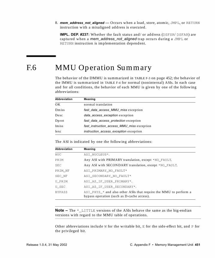
8. mem_address_not_aligned — Occurs when a load, store, atomic, JMPL, or RETURN instruction with a misaligned address is executed.
IMPL. DEP. #237: Whether the fault status and/or address (DSFSR/DSFAR) are captured when a mem_address_not_aligned trap occurs during a JMPL or RETURN instruction is implementation dependent.
F.6 MMU Operation SummaryThe behavior of the DMMU is summarized in TABLE F-3 on page 452; the behavior of the IMMU is summarized in TABLE F-4 for normal (noninternal) ASIs. In each case and for all conditions, the behavior of each MMU is given by one of the following abbreviations:
The ASI is indicated by one the following abbreviations:
Note – The *_LITTLE versions of the ASIs behave the same as the big-endian versions with regard to the MMU table of operations.
Other abbreviations include W for the writable bit, E for the side-effect bit, and P for the privileged bit.
Abbreviation Meaning
OK normal translation
Dmiss fast_data_access_MMU_miss exception
Dexc data_access_exception exception
Dprot fast_data_access_protection exception
Imiss fast_instruction_access_MMU_miss exception
Iexc instruction_access_exception exception
Abbreviation Meaning
NUC ASI_NUCLEUS*.
PRIM Any ASI with PRIMARY translation, except *NO_FAULT.
SEC Any ASI with SECONDARY translation, except *NO_FAULT.
PRIM_NF ASI_PRIMARY_NO_FAULT*
SEC_NF ASI_SECONDARY_NO_FAULT*
U_PRIM ASI_AS_IF_USER_PRIMARY*.
U_SEC ASI_AS_IF_USER_SECONDARY*.
BYPASS ASI_PHYS_* and also other ASIs that require the MMU to perform a bypass operation (such as D-cache access).
Release 1.0.4, 31 May 2002 C. Appendix F • Memory Management Unit 451
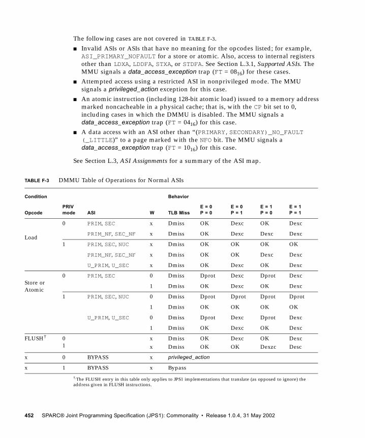
The following cases are not covered in TABLE F-3.
■ Invalid ASIs or ASIs that have no meaning for the opcodes listed; for example, ASI_PRIMARY_NOFAULT for a store or atomic. Also, access to internal registers other than LDXA, LDDFA, STXA, or STDFA. See Section L.3.1, Supported ASIs. The MMU signals a data_access_exception trap (FT = 0816) for these cases.
■ Attempted access using a restricted ASI in nonprivileged mode. The MMU signals a privileged_action exception for this case.
■ An atomic instruction (including 128-bit atomic load) issued to a memory address marked noncacheable in a physical cache; that is, with the CP bit set to 0, including cases in which the DMMU is disabled. The MMU signals a data_access_exception trap (FT = 0416) for this case.
■ A data access with an ASI other than “(PRIMARY,SECONDARY)_NO_FAULT (_LITTLE)” to a page marked with the NFO bit. The MMU signals a data_access_exception trap (FT = 1016) for this case.
See Section L.3, ASI Assignments for a summary of the ASI map.
TABLE F-3 DMMU Table of Operations for Normal ASIs
Condition Behavior
OpcodePRIV mode ASI W TLB Miss
E = 0P = 0
E = 0P = 1
E = 1P = 0
E = 1P = 1
Load
0 PRIM, SEC x Dmiss OK Dexc OK Dexc
PRIM_NF, SEC_NF x Dmiss OK Dexc Dexc Dexc
1 PRIM, SEC, NUC x Dmiss OK OK OK OK
PRIM_NF, SEC_NF x Dmiss OK OK Dexc Dexc
U_PRIM, U_SEC x Dmiss OK Dexc OK Dexc
Store or Atomic
0 PRIM, SEC 0 Dmiss Dprot Dexc Dprot Dexc
1 Dmiss OK Dexc OK Dexc
1 PRIM, SEC, NUC 0 Dmiss Dprot Dprot Dprot Dprot
1 Dmiss OK OK OK OK
U_PRIM, U_SEC 0 Dmiss Dprot Dexc Dprot Dexc
1 Dmiss OK Dexc OK Dexc
FLUSH†
†.The FLUSH entry in this table only applies to JPS1 implementations that translate (as opposed to ignore) theaddress given in FLUSH instructions.
01
xx
DmissDmiss
OKOK
DexcOK
OKDexzc
DexcDesc
x 0 BYPASS x privileged_action
x 1 BYPASS x Bypass
452 SPARC® Joint Programming Specification (JPS1): Commonality • Release 1.0.4, 31 May 2002
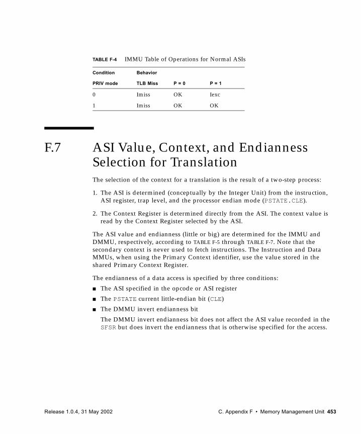
F.7 ASI Value, Context, and Endianness Selection for TranslationThe selection of the context for a translation is the result of a two-step process:
1. The ASI is determined (conceptually by the Integer Unit) from the instruction, ASI register, trap level, and the processor endian mode (PSTATE.CLE).
2. The Context Register is determined directly from the ASI. The context value is read by the Context Register selected by the ASI.
The ASI value and endianness (little or big) are determined for the IMMU and DMMU, respectively, according to TABLE F-5 through TABLE F-7. Note that the secondary context is never used to fetch instructions. The Instruction and Data MMUs, when using the Primary Context identifier, use the value stored in the shared Primary Context Register.
The endianness of a data access is specified by three conditions:
■ The ASI specified in the opcode or ASI register
■ The PSTATE current little-endian bit (CLE)
■ The DMMU invert endianness bit
The DMMU invert endianness bit does not affect the ASI value recorded in the SFSR but does invert the endianness that is otherwise specified for the access.
TABLE F-4 IMMU Table of Operations for Normal ASIs
Condition Behavior
PRIV mode TLB Miss P = 0 P = 1
0 Imiss OK Iexc
1 Imiss OK OK
Release 1.0.4, 31 May 2002 C. Appendix F • Memory Management Unit 453
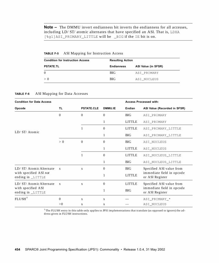
Note – The DMMU invert endianness bit inverts the endianness for all accesses, including LD/ST/atomic alternates that have specified an ASI. That is, LDXA [%g1]ASI_PRIMARY_LITTLE will be _BIG if the IE bit is on.
TABLE F-5 ASI Mapping for Instruction Access
Condition for Instruction Access Resulting Action
PSTATE.TL Endianness ASI Value (in SFSR)
0 BIG ASI_PRIMARY
> 0 BIG ASI_NUCLEUS
TABLE F-6 ASI Mapping for Data Accesses
Condition for Data Access Access Processed with:
Opcode TL PSTATE.CLE DMMU.IE Endian ASI Value (Recorded in SFSR)
LD/ST/Atomic
0 0 0 BIG ASI_PRIMARY
1 LITTLE ASI_PRIMARY
1 0 LITTLE ASI_PRIMARY_LITTLE
1 BIG ASI_PRIMARY_LITTLE
> 0 0 0 BIG ASI_NUCLEUS
1 LITTLE ASI_NUCLEUS
1 0 LITTLE ASI_NUCLEUS_LITTLE
1 BIG ASI_NUCLEUS_LITTLE
LD/ST/Atomic Alternate with specified ASI not ending in _LITTLE
x x 0 BIG Specified ASI value from immediate field in opcode or ASI Register1 LITTLE
LD/ST/Atomic Alternate with specified ASI ending in _LITTLE
x x 0 LITTLE Specified ASI value from immediate field in opcode or ASI Register1 BIG
FLUSH†
†.The FLUSH entry in this table only applies to JPS1 implementations that translate (as opposed to ignore) the ad-dress given in FLUSH instructions.
0>0
xx
xx
——
ASI_PRIMARY_*
ASI_NUCLEUS
454 SPARC® Joint Programming Specification (JPS1): Commonality • Release 1.0.4, 31 May 2002
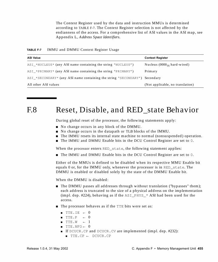
The Context Register used by the data and instruction MMUs is determined according to TABLE F-7. The Context Register selection is not affected by the endianness of the access. For a comprehensive list of ASI values in the ASI map, see Appendix L, Address Space Identifiers.
F.8 Reset, Disable, and RED_state Behavior During global reset of the processor, the following statements apply:
■ No change occurs in any block of the DMMU.■ No change occurs in the datapath or TLB blocks of the IMMU.■ The IMMU resets its internal state machine to normal (nonsuspended) operation.■ The IMMU and DMMU Enable bits in the DCU Control Register are set to 0.
When the processor enters RED_state, the following statement applies:
■ The IMMU and DMMU Enable bits in the DCU Control Register are set to 0.
Either of the MMUs is defined to be disabled when its respective MMU Enable bit equals 0 or, for the IMMU only, whenever the processor is in RED_state. The DMMU is enabled or disabled solely by the state of the DMMU Enable bit.
When the DMMU is disabled:
■ The DMMU passes all addresses through without translation ("bypasses" them); each address is truncated to the size of a physical address on the implementation (impl. dep. #224), behaving as if the ASI_PHYS_* ASI had been used for the access.
■ The processor behaves as if the TTE bits were set as:
■ TTE.IE ← 0■ TTE.P ← 0■ TTE.W ← 1■ TTE.NFO← 0■ If DCUCR.CP and DCUCR.CV are implemented (impl. dep. #232):
■ TTE.CP ← DCUCR.CP
TABLE F-7 IMMU and DMMU Context Register Usage
ASI Value Context Register
ASI_*NUCLEUS* (any ASI name containing the string “NUCLEUS”) Nucleus (000016 hard-wired)
ASI_*PRIMARY* (any ASI name containing the string “PRIMARY”) Primary
ASI_*SECONDARY* (any ASI name containing the string “SECONDARY”) Secondary
All other ASI values (Not applicable, no translation)
Release 1.0.4, 31 May 2002 C. Appendix F • Memory Management Unit 455
■ TTE.CV ← DCUCR.CV■ TTE.E ← not DCUCR.CP
■ If DCUCR.CP and DCUCR.CV are not implemented:■ TTE.E ← not TTE.CP
IMPL. DEP. #231: The variability of the width of physical address is implementation dependent in JPS1, and if variable, the initial width of the physical address after reset is also implementation dependent in JPS1.
IMPL. DEP. #232: Whether CP and CV bits exist in the DCU Control Register is implementation dependent in JPS1.
However, if a bypass ASI (ASI_PHYS_*) is used while the DMMU is disabled, the bypass operation behaves as it does when the DMMU is enabled; that is, the access is processed with the E, CP, and CV bits as specified by the bypass ASI (see TABLE F-15 on page 472).
When the IMMU is disabled, it truncates all instruction accesses to the physical address size (implementation dependent) and passes the default physically cacheable bit or implementation-dependent Data Cache Unit Control Register CP bit to the cache system. The access does not generate an instruction_access_exception trap.
When disabled, both the IMMU and DMMU correctly perform all LDXA and STXA operations to internal registers, and traps are signalled just as if the MMU were enabled. For instance, if a nonfaulting load is issued when the DMMU is disabled and DCUCR.CP is set to 0 if the implementation has the bit, then the DMMU signals a data_access_exception trap (FT = 0216), since E is set to 1.
IMPL. DEP. #117: Whether PREFETCH and nonfaulting loads always succeed when the MMU is disabled is implementation dependent.
Note – A reset of the TLB is not performed by a chip reset or by entry into RED_state. Before the MMUs are enabled, the operating system software must explicitly write each entry with either a valid TLB entry or an entry with the valid bit set to 0. The operation of the IMMU or DMMU in enabled mode is undefined if the TLB valid bits have not been set explicitly beforehand.
456 SPARC® Joint Programming Specification (JPS1): Commonality • Release 1.0.4, 31 May 2002
F.9 SPARC V9 “MMU Requirements” AnnexThe MMU complies completely with the SPARC V9 “MMU Requirements” Annex. TABLE F-8 shows how various protection modes can be achieved, if necessary, through the presence or absence of a translation in the instruction or data MMU. Note that this behavior requires specialized TLB-miss handler code to guarantee these conditions.
F.10 Internal Registers and ASI OperationsIn this section, how to access MMU registers is described, followed by descriptions of the registers themselves, as follows:
■ Context Registers■ Instruction/Data MMU TLB Tag Access Registers■ I/D TLB Data In, Data Access, and Tag Read Registers■ I/D TSB Tag Target Registers■ I/D TSB Base Registers■ I/D TSB Extension Registers■ I/D TSB 8-Kbyte and 64-Kbyte Pointer and Direct Pointer Registers■ I/D Synchronous Fault Status Registers (I-SFSR, D-SFSR)■ MMU Data Synchronous Fault Address Register
The I/D demap operation is then described.
TABLE F-8 MMU SPARC V9 Annex G Protection Mode Compliance
Condition
ResultantProtection Mode
TTE in DMMU
TTE inIMMU
Writable Attribute Bit
Yes No 0 Read-only
No Yes N/A Execute-only
Yes No 1 Read/Write
Yes Yes 0 Read-only/Execute
Yes Yes 1 Read/Write/Execute
Release 1.0.4, 31 May 2002 C. Appendix F • Memory Management Unit 457
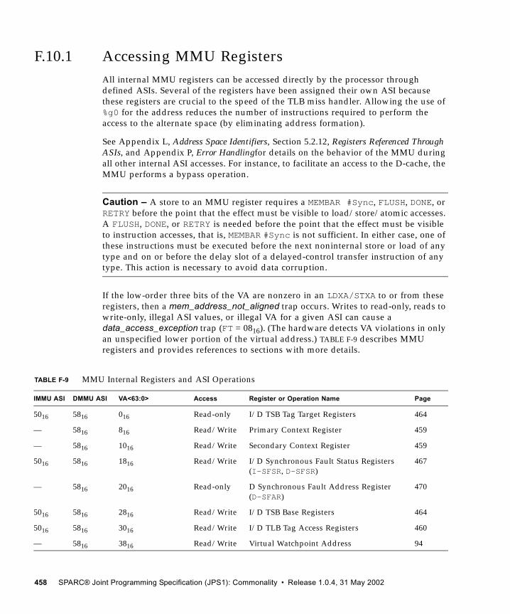
F.10.1 Accessing MMU RegistersAll internal MMU registers can be accessed directly by the processor through defined ASIs. Several of the registers have been assigned their own ASI because these registers are crucial to the speed of the TLB miss handler. Allowing the use of %g0 for the address reduces the number of instructions required to perform the access to the alternate space (by eliminating address formation).
See Appendix L, Address Space Identifiers, Section 5.2.12, Registers Referenced Through ASIs, and Appendix P, Error Handlingfor details on the behavior of the MMU during all other internal ASI accesses. For instance, to facilitate an access to the D-cache, the MMU performs a bypass operation.
Caution – A store to an MMU register requires a MEMBAR #Sync, FLUSH, DONE, or RETRY before the point that the effect must be visible to load/store/atomic accesses. A FLUSH, DONE, or RETRY is needed before the point that the effect must be visible to instruction accesses, that is, MEMBAR #Sync is not sufficient. In either case, one of these instructions must be executed before the next noninternal store or load of any type and on or before the delay slot of a delayed-control transfer instruction of any type. This action is necessary to avoid data corruption.
If the low-order three bits of the VA are nonzero in an LDXA/STXA to or from these registers, then a mem_address_not_aligned trap occurs. Writes to read-only, reads to write-only, illegal ASI values, or illegal VA for a given ASI can cause a data_access_exception trap (FT = 0816). (The hardware detects VA violations in only an unspecified lower portion of the virtual address.) TABLE F-9 describes MMU registers and provides references to sections with more details.
TABLE F-9 MMU Internal Registers and ASI Operations
IMMU ASI DMMU ASI VA<63:0> Access Register or Operation Name Page
5016 5816 016 Read-only I/D TSB Tag Target Registers 464
— 5816 816 Read/Write Primary Context Register 459
— 5816 1016 Read/Write Secondary Context Register 459
5016 5816 1816 Read/Write I/D Synchronous Fault Status Registers (I-SFSR, D-SFSR)
467
— 5816 2016 Read-only D Synchronous Fault Address Register (D-SFAR)
470
5016 5816 2816 Read/Write I/D TSB Base Registers 464
5016 5816 3016 Read/Write I/D TLB Tag Access Registers 460
— 5816 3816 Read/Write Virtual Watchpoint Address 94
458 SPARC® Joint Programming Specification (JPS1): Commonality • Release 1.0.4, 31 May 2002
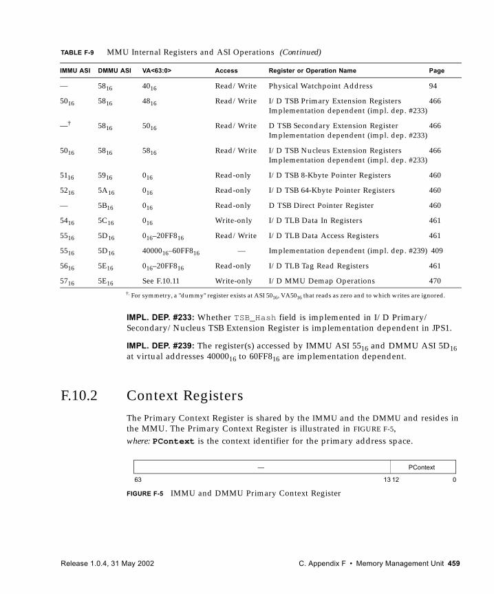
IMPL. DEP. #233: Whether TSB_Hash field is implemented in I/D Primary/Secondary/Nucleus TSB Extension Register is implementation dependent in JPS1.
IMPL. DEP. #239: The register(s) accessed by IMMU ASI 5516 and DMMU ASI 5D16 at virtual addresses 4000016 to 60FF816 are implementation dependent.
F.10.2 Context Registers The Primary Context Register is shared by the IMMU and the DMMU and resides in the MMU. The Primary Context Register is illustrated in FIGURE F-5,where: PContext is the context identifier for the primary address space.
FIGURE F-5 IMMU and DMMU Primary Context Register
— 5816 4016 Read/Write Physical Watchpoint Address 94
5016 5816 4816 Read/Write I/D TSB Primary Extension RegistersImplementation dependent (impl. dep. #233)
466
—† 5816 5016 Read/Write D TSB Secondary Extension RegisterImplementation dependent (impl. dep. #233)
466
5016 5816 5816 Read/Write I/D TSB Nucleus Extension RegistersImplementation dependent (impl. dep. #233)
466
5116 5916 016 Read-only I/D TSB 8-Kbyte Pointer Registers 460
5216 5A16 016 Read-only I/D TSB 64-Kbyte Pointer Registers 460
— 5B16 016 Read-only D TSB Direct Pointer Register 460
5416 5C16 016 Write-only I/D TLB Data In Registers 461
5516 5D16 016–20FF816 Read/Write I/D TLB Data Access Registers 461
5516 5D16 4000016–60FF816 — Implementation dependent (impl. dep. #239) 409
5616 5E16 016–20FF816 Read-only I/D TLB Tag Read Registers 461
5716 5E16 See F.10.11 Write-only I/D MMU Demap Operations 470
†. For symmetry, a "dummy" register exists at ASI 5016, VA5016 that reads as zero and to which writes are ignored.
TABLE F-9 MMU Internal Registers and ASI Operations (Continued)
IMMU ASI DMMU ASI VA<63:0> Access Register or Operation Name Page
63 13 12 0
— PContext
Release 1.0.4, 31 May 2002 C. Appendix F • Memory Management Unit 459
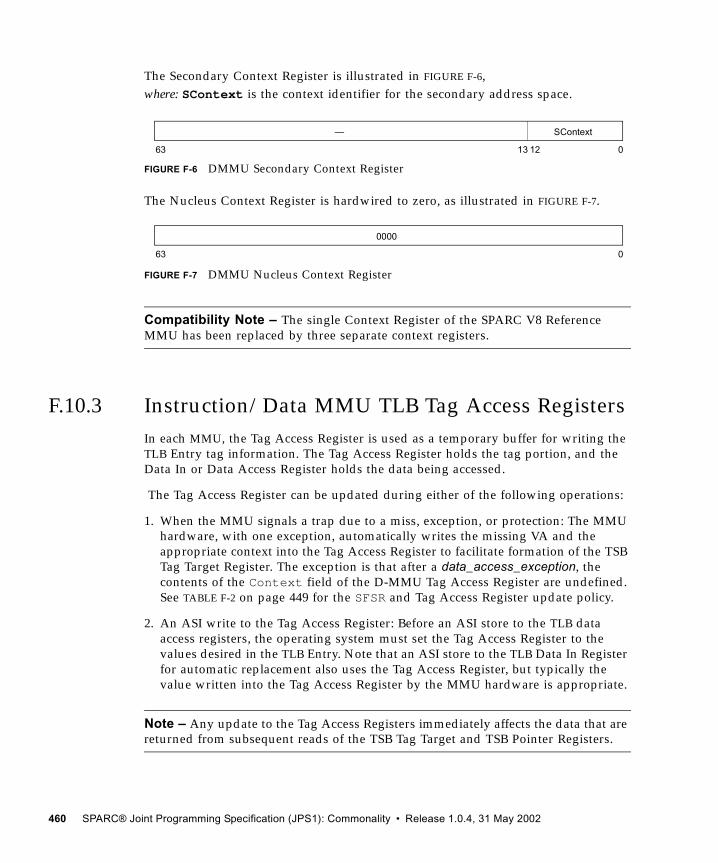
The Secondary Context Register is illustrated in FIGURE F-6,where: SContext is the context identifier for the secondary address space.
FIGURE F-6 DMMU Secondary Context Register
The Nucleus Context Register is hardwired to zero, as illustrated in FIGURE F-7.
FIGURE F-7 DMMU Nucleus Context Register
Compatibility Note – The single Context Register of the SPARC V8 Reference MMU has been replaced by three separate context registers.
F.10.3 Instruction/Data MMU TLB Tag Access RegistersIn each MMU, the Tag Access Register is used as a temporary buffer for writing the TLB Entry tag information. The Tag Access Register holds the tag portion, and the Data In or Data Access Register holds the data being accessed.
The Tag Access Register can be updated during either of the following operations:
1. When the MMU signals a trap due to a miss, exception, or protection: The MMU hardware, with one exception, automatically writes the missing VA and the appropriate context into the Tag Access Register to facilitate formation of the TSB Tag Target Register. The exception is that after a data_access_exception, the contents of the Context field of the D-MMU Tag Access Register are undefined. See TABLE F-2 on page 449 for the SFSR and Tag Access Register update policy.
2. An ASI write to the Tag Access Register: Before an ASI store to the TLB data access registers, the operating system must set the Tag Access Register to the values desired in the TLB Entry. Note that an ASI store to the TLB Data In Register for automatic replacement also uses the Tag Access Register, but typically the value written into the Tag Access Register by the MMU hardware is appropriate.
Note – Any update to the Tag Access Registers immediately affects the data that are returned from subsequent reads of the TSB Tag Target and TSB Pointer Registers.
63 13 12 0
— SContext
63 0
0000
460 SPARC® Joint Programming Specification (JPS1): Commonality • Release 1.0.4, 31 May 2002
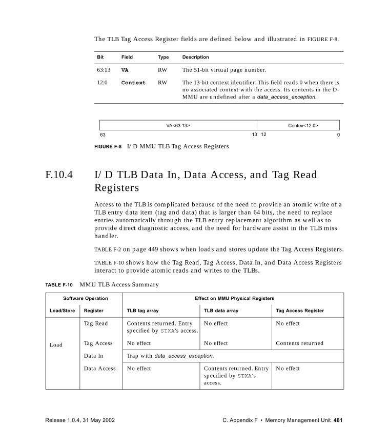
The TLB Tag Access Register fields are defined below and illustrated in FIGURE F-8.
FIGURE F-8 I/D MMU TLB Tag Access Registers
F.10.4 I/D TLB Data In, Data Access, and Tag Read RegistersAccess to the TLB is complicated because of the need to provide an atomic write of a TLB entry data item (tag and data) that is larger than 64 bits, the need to replace entries automatically through the TLB entry replacement algorithm as well as to provide direct diagnostic access, and the need for hardware assist in the TLB miss handler.
TABLE F-2 on page 449 shows when loads and stores update the Tag Access Registers.
TABLE F-10 shows how the Tag Read, Tag Access, Data In, and Data Access Registers interact to provide atomic reads and writes to the TLBs.
Bit Field Type Description
63:13 VA RW The 51-bit virtual page number.
12:0 Context RW The 13-bit context identifier. This field reads 0 when there is no associated context with the access. Its contents in the D-MMU are undefined after a data_access_exception.
TABLE F-10 MMU TLB Access Summary
Software Operation Effect on MMU Physical Registers
Load/Store Register TLB tag array TLB data array Tag Access Register
Load
Tag Read Contents returned. Entry specified by STXA‘s access.
No effect No effect
Tag Access No effect No effect Contents returned
Data In Trap with data_access_exception.
Data Access No effect Contents returned. Entry specified by STXA‘s access.
No effect
63 0
VA<63:13> Contex<12:0>
13 12
Release 1.0.4, 31 May 2002 C. Appendix F • Memory Management Unit 461
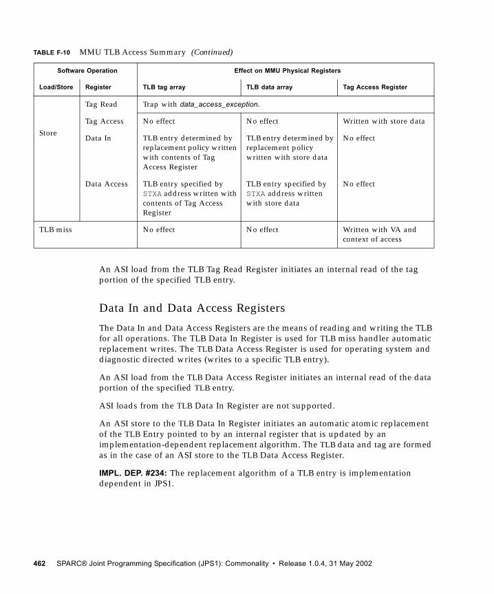
An ASI load from the TLB Tag Read Register initiates an internal read of the tag portion of the specified TLB entry.
Data In and Data Access Registers
The Data In and Data Access Registers are the means of reading and writing the TLB for all operations. The TLB Data In Register is used for TLB miss handler automatic replacement writes. The TLB Data Access Register is used for operating system and diagnostic directed writes (writes to a specific TLB entry).
An ASI load from the TLB Data Access Register initiates an internal read of the data portion of the specified TLB entry.
ASI loads from the TLB Data In Register are not supported.
An ASI store to the TLB Data In Register initiates an automatic atomic replacement of the TLB Entry pointed to by an internal register that is updated by an implementation-dependent replacement algorithm. The TLB data and tag are formed as in the case of an ASI store to the TLB Data Access Register.
IMPL. DEP. #234: The replacement algorithm of a TLB entry is implementation dependent in JPS1.
Store
Tag Read Trap with data_access_exception.
Tag Access No effect No effect Written with store data
Data In TLB entry determined by replacement policy written with contents of Tag Access Register
TLB entry determined by replacement policy written with store data
No effect
Data Access TLB entry specified by STXA address written with contents of Tag Access Register
TLB entry specified by STXA address written with store data
No effect
TLB miss No effect No effect Written with VA and context of access
TABLE F-10 MMU TLB Access Summary (Continued)
Software Operation Effect on MMU Physical Registers
Load/Store Register TLB tag array TLB data array Tag Access Register
462 SPARC® Joint Programming Specification (JPS1): Commonality • Release 1.0.4, 31 May 2002
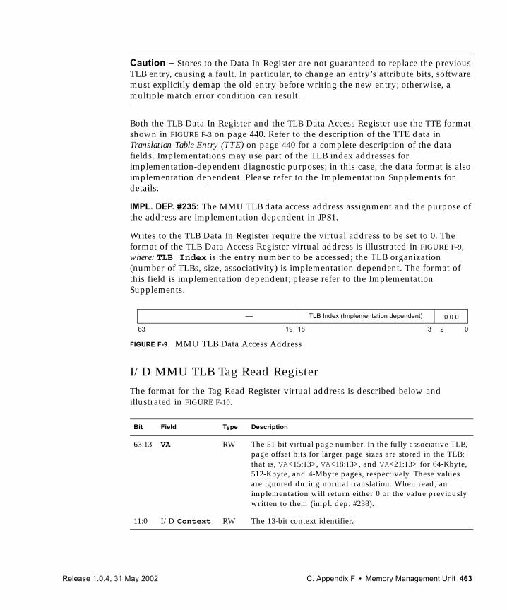
Caution – Stores to the Data In Register are not guaranteed to replace the previous TLB entry, causing a fault. In particular, to change an entry’s attribute bits, software must explicitly demap the old entry before writing the new entry; otherwise, a multiple match error condition can result.
Both the TLB Data In Register and the TLB Data Access Register use the TTE format shown in FIGURE F-3 on page 440. Refer to the description of the TTE data in Translation Table Entry (TTE) on page 440 for a complete description of the data fields. Implementations may use part of the TLB index addresses for implementation-dependent diagnostic purposes; in this case, the data format is also implementation dependent. Please refer to the Implementation Supplements for details.
IMPL. DEP. #235: The MMU TLB data access address assignment and the purpose of the address are implementation dependent in JPS1.
Writes to the TLB Data In Register require the virtual address to be set to 0. The format of the TLB Data Access Register virtual address is illustrated in FIGURE F-9, where: TLB Index is the entry number to be accessed; the TLB organization (number of TLBs, size, associativity) is implementation dependent. The format of this field is implementation dependent; please refer to the Implementation Supplements.
FIGURE F-9 MMU TLB Data Access Address
I/D MMU TLB Tag Read RegisterThe format for the Tag Read Register virtual address is described below and illustrated in FIGURE F-10.
Bit Field Type Description
63:13 VA RW The 51-bit virtual page number. In the fully associative TLB, page offset bits for larger page sizes are stored in the TLB; that is, VA<15:13>, VA<18:13>, and VA<21:13> for 64-Kbyte, 512-Kbyte, and 4-Mbyte pages, respectively. These values are ignored during normal translation. When read, an implementation will return either 0 or the value previously written to them (impl. dep. #238).
11:0 I/D Context RW The 13-bit context identifier.
63 0
0 0 0
3 2
— TLB Index (Implementation dependent)
1819
Release 1.0.4, 31 May 2002 C. Appendix F • Memory Management Unit 463
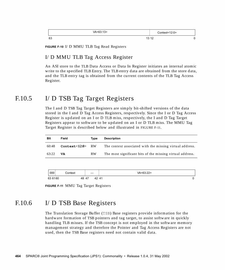
FIGURE F-10 I/D MMU TLB Tag Read Registers
I/D MMU TLB Tag Access Register
An ASI store to the TLB Data Access or Data In Register initiates an internal atomic write to the specified TLB Entry. The TLB entry data are obtained from the store data, and the TLB entry tag is obtained from the current contents of the TLB Tag Access Register.
F.10.5 I/D TSB Tag Target RegistersThe I and D TSB Tag Target Registers are simply bit-shifted versions of the data stored in the I and D Tag Access Registers, respectively. Since the I or D Tag Access Register is updated on an I or D TLB miss, respectively, the I and D Tag Target Registers appear to software to be updated on an I or D TLB miss. The MMU Tag Target Register is described below and illustrated in FIGURE F-11.
FIGURE F-11 MMU Tag Target Registers
F.10.6 I/D TSB Base RegistersThe Translation Storage Buffer (TSB) Base registers provide information for the hardware formation of TSB pointers and tag target, to assist software in quickly handling TLB misses. If the TSB concept is not employed in the software memory management strategy and therefore the Pointer and Tag Access Registers are not used, then the TSB Base registers need not contain valid data.
BIt Field Type Description
60:48 Context<12:0> RW The context associated with the missing virtual address.
63:22 VA RW The most significant bits of the missing virtual address.
63 013 12
Context<12:0>VA<63:13>
63 61 47 4160 48 42 0
Context000 — VA<63:22>
464 SPARC® Joint Programming Specification (JPS1): Commonality • Release 1.0.4, 31 May 2002
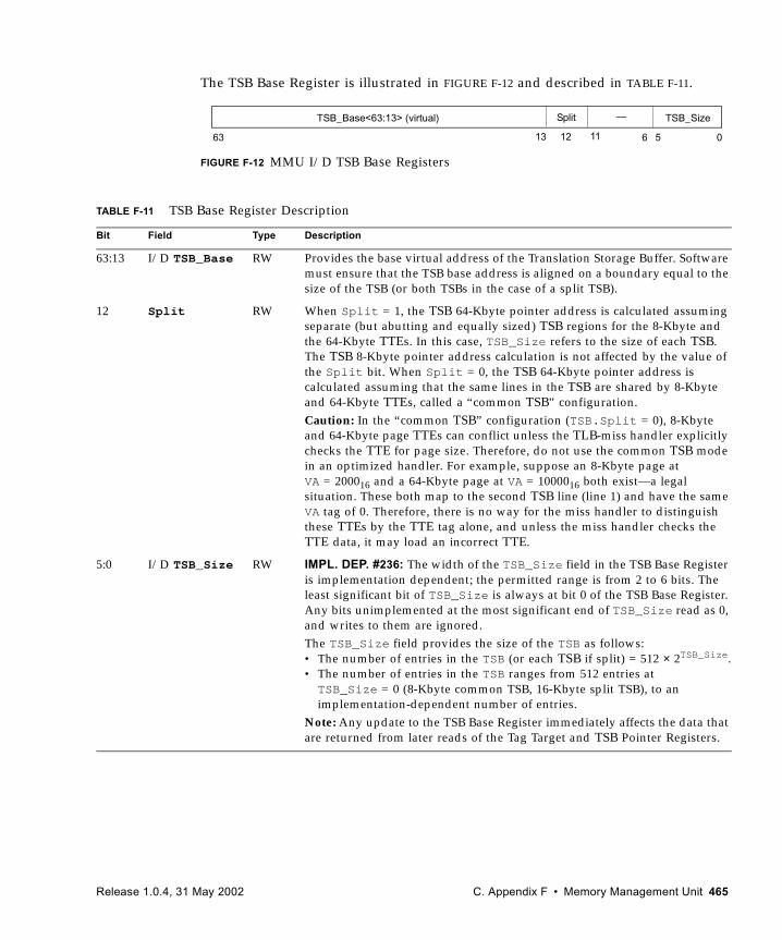
The TSB Base Register is illustrated in FIGURE F-12 and described in TABLE F-11.
FIGURE F-12 MMU I/D TSB Base Registers
TABLE F-11 TSB Base Register Description
Bit Field Type Description
63:13 I/D TSB_Base RW Provides the base virtual address of the Translation Storage Buffer. Software must ensure that the TSB base address is aligned on a boundary equal to the size of the TSB (or both TSBs in the case of a split TSB).
12 Split RW When Split = 1, the TSB 64-Kbyte pointer address is calculated assuming separate (but abutting and equally sized) TSB regions for the 8-Kbyte and the 64-Kbyte TTEs. In this case, TSB_Size refers to the size of each TSB. The TSB 8-Kbyte pointer address calculation is not affected by the value of the Split bit. When Split = 0, the TSB 64-Kbyte pointer address is calculated assuming that the same lines in the TSB are shared by 8-Kbyte and 64-Kbyte TTEs, called a “common TSB” configuration.Caution: In the “common TSB” configuration (TSB.Split = 0), 8-Kbyte and 64-Kbyte page TTEs can conflict unless the TLB-miss handler explicitly checks the TTE for page size. Therefore, do not use the common TSB mode in an optimized handler. For example, suppose an 8-Kbyte page at VA = 200016 and a 64-Kbyte page at VA = 1000016 both exist—a legal situation. These both map to the second TSB line (line 1) and have the same VA tag of 0. Therefore, there is no way for the miss handler to distinguish these TTEs by the TTE tag alone, and unless the miss handler checks the TTE data, it may load an incorrect TTE.
5:0 I/D TSB_Size RW IMPL. DEP. #236: The width of the TSB_Size field in the TSB Base Register is implementation dependent; the permitted range is from 2 to 6 bits. The least significant bit of TSB_Size is always at bit 0 of the TSB Base Register. Any bits unimplemented at the most significant end of TSB_Size read as 0, and writes to them are ignored.The TSB_Size field provides the size of the TSB as follows:• The number of entries in the TSB (or each TSB if split) = 512 × 2TSB_Size.• The number of entries in the TSB ranges from 512 entries at TSB_Size = 0 (8-Kbyte common TSB, 16-Kbyte split TSB), to an implementation-dependent number of entries.
Note: Any update to the TSB Base Register immediately affects the data that are returned from later reads of the Tag Target and TSB Pointer Registers.
63 6 5 0
TSB_Base<63:13> (virtual) TSB_Size
13 12
Split —
11
Release 1.0.4, 31 May 2002 C. Appendix F • Memory Management Unit 465
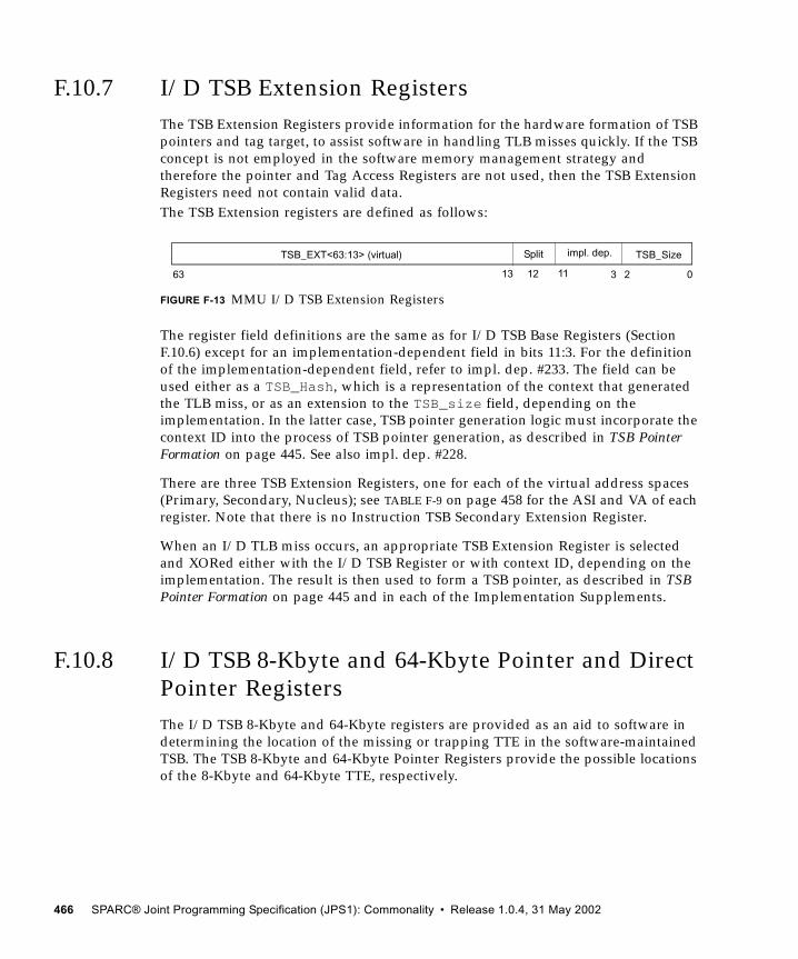
F.10.7 I/D TSB Extension RegistersThe TSB Extension Registers provide information for the hardware formation of TSB pointers and tag target, to assist software in handling TLB misses quickly. If the TSB concept is not employed in the software memory management strategy and therefore the pointer and Tag Access Registers are not used, then the TSB Extension Registers need not contain valid data.The TSB Extension registers are defined as follows:
FIGURE F-13 MMU I/D TSB Extension Registers
The register field definitions are the same as for I/D TSB Base Registers (Section F.10.6) except for an implementation-dependent field in bits 11:3. For the definition of the implementation-dependent field, refer to impl. dep. #233. The field can be used either as a TSB_Hash, which is a representation of the context that generated the TLB miss, or as an extension to the TSB_size field, depending on the implementation. In the latter case, TSB pointer generation logic must incorporate the context ID into the process of TSB pointer generation, as described in TSB Pointer Formation on page 445. See also impl. dep. #228.
There are three TSB Extension Registers, one for each of the virtual address spaces (Primary, Secondary, Nucleus); see TABLE F-9 on page 458 for the ASI and VA of each register. Note that there is no Instruction TSB Secondary Extension Register.
When an I/D TLB miss occurs, an appropriate TSB Extension Register is selected and XORed either with the I/D TSB Register or with context ID, depending on the implementation. The result is then used to form a TSB pointer, as described in TSB Pointer Formation on page 445 and in each of the Implementation Supplements.
F.10.8 I/D TSB 8-Kbyte and 64-Kbyte Pointer and Direct Pointer RegistersThe I/D TSB 8-Kbyte and 64-Kbyte registers are provided as an aid to software in determining the location of the missing or trapping TTE in the software-maintained TSB. The TSB 8-Kbyte and 64-Kbyte Pointer Registers provide the possible locations of the 8-Kbyte and 64-Kbyte TTE, respectively.
63 3 2 0
TSB_EXT<63:13> (virtual) TSB_Size
13 12
Split impl. dep.
11
466 SPARC® Joint Programming Specification (JPS1): Commonality • Release 1.0.4, 31 May 2002
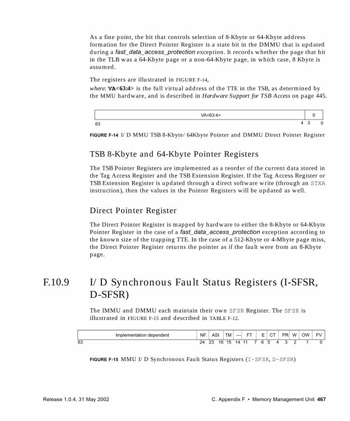
As a fine point, the bit that controls selection of 8-Kbyte or 64-Kbyte address formation for the Direct Pointer Register is a state bit in the DMMU that is updated during a fast_data_access_protection exception. It records whether the page that hit in the TLB was a 64-Kbyte page or a non-64-Kbyte page, in which case, 8 Kbyte is assumed.
The registers are illustrated in FIGURE F-14,where: VA<63:4> is the full virtual address of the TTE in the TSB, as determined by the MMU hardware, and is described in Hardware Support for TSB Access on page 445.
FIGURE F-14 I/D MMU TSB 8-Kbyte/64Kbyte Pointer and DMMU Direct Pointer Register
TSB 8-Kbyte and 64-Kbyte Pointer Registers
The TSB Pointer Registers are implemented as a reorder of the current data stored in the Tag Access Register and the TSB Extension Register. If the Tag Access Register or TSB Extension Register is updated through a direct software write (through an STXA instruction), then the values in the Pointer Registers will be updated as well.
Direct Pointer Register
The Direct Pointer Register is mapped by hardware to either the 8-Kbyte or 64-Kbyte Pointer Register in the case of a fast_data_access_protection exception according to the known size of the trapping TTE. In the case of a 512-Kbyte or 4-Mbyte page miss, the Direct Pointer Register returns the pointer as if the fault were from an 8-Kbyte page.
F.10.9 I/D Synchronous Fault Status Registers (I-SFSR, D-SFSR)The IMMU and DMMU each maintain their own SFSR Register. The SFSR is illustrated in FIGURE F-15 and described in TABLE F-12.
FIGURE F-15 MMU I/D Synchronous Fault Status Registers (I-SFSR, D-SFSR)
63 0
VA<63:4>
4 3
0
63 1523 1114 7 5 3 16 4 2 0
Implementation dependent ASI FT E W OW FVCT PR
24
—
16
TMNF.
Release 1.0.4, 31 May 2002 C. Appendix F • Memory Management Unit 467
TABLE F-12 SFSR Bit Description
Bit Field Type Description
63:25 — Implementation dependent. Refer to Implementation Supplements.
24 NF RW Set in the DMMU if the faulting instruction was a nonfaulting load (a load to ASI_NOFAULT) (IMMU = 0). NF is always 0 in I-SFSR.
23:16 ASI RW Records the 8-bit ASI associated with the faulting instruction. This field is valid for both DMMU and IMMU SFSRs and for all traps in which the FV bit is set. A trapping alternate space load or store sets the ASI field to the ASI the instruction attempted to reference. A trapping non-alternate-space load or store sets ASI to ASI_PRIMARY if PSTATE.CLE = 0 or to ASI_PRIMARY_LITTLE if PSTATE.CLE = 1. A mem_address_not_aligned trap caused by a JMPL or RETURN either does not set DSFSR.ASI or sets it as would a trapping non-alternate-space load or store. (impl. dep. #237)
15 TM RW I/D TLB miss.
11:7 FT RW Specifies the exact condition that caused the recorded fault, according to TABLE F-13 following this table. In the DMMU, the Fault Type field is valid only for data_access_exception faults; there is no ambiguity in all other MMU trap cases. Note that the hardware does not priority-encode the bits set in the fault type (FT) field; that is, multiple bits can be set. In particular, the following ASI stores could set both the 0116 and 0816 Fault Type bits (the page is privileged, as well as storing to a read-only ASI):stda %g0, [%g4]ASI_PRIMARY_NO_FAULT stda %g0, [%g4]ASI_SECONDARY_NO_FAULT stda %g0, [%g4]ASI_PRIMARY_NO_FAULT_LITTLE stda %g0, [%g4]ASI_SECONDARY_NO_FAULT_LITTLE The FT field in the IMMU SFSR always reads 0 for fast_instruction_access_MMU_miss and reads 0116 for instruction_access_exception, as all other fault types do not apply.
6 E RW Side-effect bit. Associated with the faulting data access or flush instruction. Set by translating ASI accesses (see Section L.2, ASI Values) that are mapped by the TLB with the E bit set and bypass ASIs 1516 and 1D16. Other cases that update the SFSR (including bypass or internal ASI accesses) set the E bit to 0. It always reads as 0 in the IMMU.
5:4 CT RW Context Register selection, as described below. The context is set to 112 when the access does not have a translating ASI.
3 PR RW Privilege bit. Set if the faulting access occurred while in privileged mode. This field is valid for all traps in which the FV bit is set.
2 W RW Write bit. Set if the faulting access indicated a data write operation (a store or atomic load/store instruction). This bit always reads as 0 in the IMMU SFSR.
Context ID IMMU Context DMMU Context
00 Primary Primary01 Reserved Secondary10 Nucleus Nucleus11 Reserved Reserved
468 SPARC® Joint Programming Specification (JPS1): Commonality • Release 1.0.4, 31 May 2002
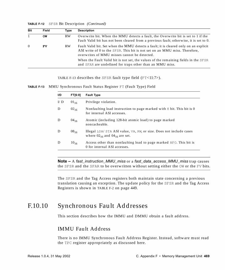
TABLE F-13 describes the SFSR fault type field (FT<11:7>).
Note – A fast_instruction_MMU_miss or a fast_data_access_MMU_miss trap causes the SFSR and the SFAR to be overwritten without setting either the OW or the FV bits.
The SFSR and the Tag Access registers both maintain state concerning a previous translation causing an exception. The update policy for the SFSR and the Tag Access Registers is shown in TABLE F-2 on page 449.
F.10.10 Synchronous Fault AddressesThis section describes how the IMMU and DMMU obtain a fault address.
IMMU Fault Address
There is no IMMU Synchronous Fault Address Register. Instead, software must read the TPC register appropriately as discussed here.
1 OW RW Overwrite bit. When the MMU detects a fault, the Overwrite bit is set to 1 if the Fault Valid bit has not been cleared from a previous fault; otherwise, it is set to 0.
0 FV RW Fault Valid bit. Set when the MMU detects a fault; it is cleared only on an explicit ASI write of 0 to the SFSR. This bit is not set on an MMU miss. Therefore, overwrites of MMU misses cannot be detected.When the Fault Valid bit is not set, the values of the remaining fields in the SFSR and SFAR are undefined for traps other than an MMU miss.
TABLE F-13 MMU Synchronous Fault Status Register FT (Fault Type) Field
I/D FT[6:0] Fault Type
I/D 0116 Privilege violation.
D 0216 Nonfaulting load instruction to page marked with E bit. This bit is 0 for internal ASI accesses.
D 0416 Atomic (including 128-bit atomic load) to page marked noncacheable.
D 0816 Illegal LDA/STA ASI value, VA, RW, or size. Does not include cases where 0216 and 0416 are set.
D 1016 Access other than nonfaulting load to page marked NFO. This bit is 0 for internal ASI accesses.
TABLE F-12 SFSR Bit Description (Continued)
Bit Field Type Description
Release 1.0.4, 31 May 2002 C. Appendix F • Memory Management Unit 469
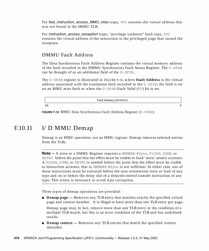
For fast_instruction_access_MMU_miss traps, TPC contains the virtual address that was not found in the IMMU TLB.
For instruction_access_exception traps, “privilege violation” fault type, TPC contains the virtual address of the instruction in the privileged page that caused the exception.
DMMU Fault Address
The Data Synchronous Fault Address Register contains the virtual memory address of the fault recorded in the DMMU Synchronous Fault Status Register. The D-SFAR can be thought of as an additional field of the D-SFSR.
The D-SFAR register is illustrated in FIGURE F-16, where Fault Address is the virtual address associated with the translation fault recorded in the D-SFSR; the field is set on an MMU miss fault or when the D-SFSR Fault Valid (FV) bit is set.
FIGURE F-16 MMU Data Synchronous Fault Address Register (D-SFAR)
F.10.11 I/D MMU DemapDemap is an MMU operation, not an MMU register. Demap removes selected entries from the TLBs.
Note – A store to a DMMU Register requires a MEMBAR #Sync, FLUSH, DONE, or RETRY before the point that the effect must be visible to load/store/atomic accesses. A FLUSH, DONE, or RETRY is needed before the point that the effect must be visible to instruction accesses, that is, MEMBAR #Sync is not sufficient. In either case, one of these instructions must be executed before the next noninternal store or load of any type and on or before the delay slot of a delayed-control transfer instruction of any type. This action is necessary to avoid data corruption.
Three types of demap operations are provided:
■ Demap page — Removes any TLB entry that matches exactly the specified virtual page and context number. It is illegal to have more than one TLB entry per page.
Demap page may, in fact, remove more than one TLB entry in the condition of a multiple TLB match, but this is an error condition of the TLB and has undefined results.
■ Demap context — Removes any TLB entries that match the specified context identifier.
63 0
Fault Address (VA<63:0>)
470 SPARC® Joint Programming Specification (JPS1): Commonality • Release 1.0.4, 31 May 2002
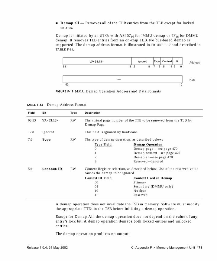
■ Demap all — Removes all of the TLB entries from the TLB except for locked entries.
Demap is initiated by an STXA with ASI 5716 for IMMU demap or 5F16 for DMMU demap. It removes TLB entries from an on-chip TLB. No bus-based demap is supported. The demap address format is illustrated in FIGURE F-17 and described in TABLE F-14.
FIGURE F-17 MMU Demap Operation Address and Data Formats
A demap operation does not invalidate the TSB in memory. Software must modify the appropriate TTEs in the TSB before initiating a demap operation.
Except for Demap All, the demap operation does not depend on the value of any entry’s lock bit. A demap operation demaps both locked entries and unlocked entries.
The demap operation produces no output.
TABLE F-14 Demap Address Format
Field Bit Type Description
63:13 VA<63:13> RW The virtual page number of the TTE to be removed from the TLB for Demap Page.
12:8 Ignored This field is ignored by hardware.
7:6 Type RW The type of demap operation, as described below:Type Field Demap Operation0 Demap page— see page 4701 Demap context—see page 4702 Demap all—see page 4703 Reserved—Ignored
5:4 Context ID RW Context Register selection, as described below. Use of the reserved value causes the demap to be ignoredContext ID Field Context Used in Demap
00 Primary01 Secondary (DMMU only)10 Nucleus11 Reserved
0Context
012Address
Data
3463 13
Ignored
7 56
Type
063
VA<63:13>
—
8
Release 1.0.4, 31 May 2002 C. Appendix F • Memory Management Unit 471
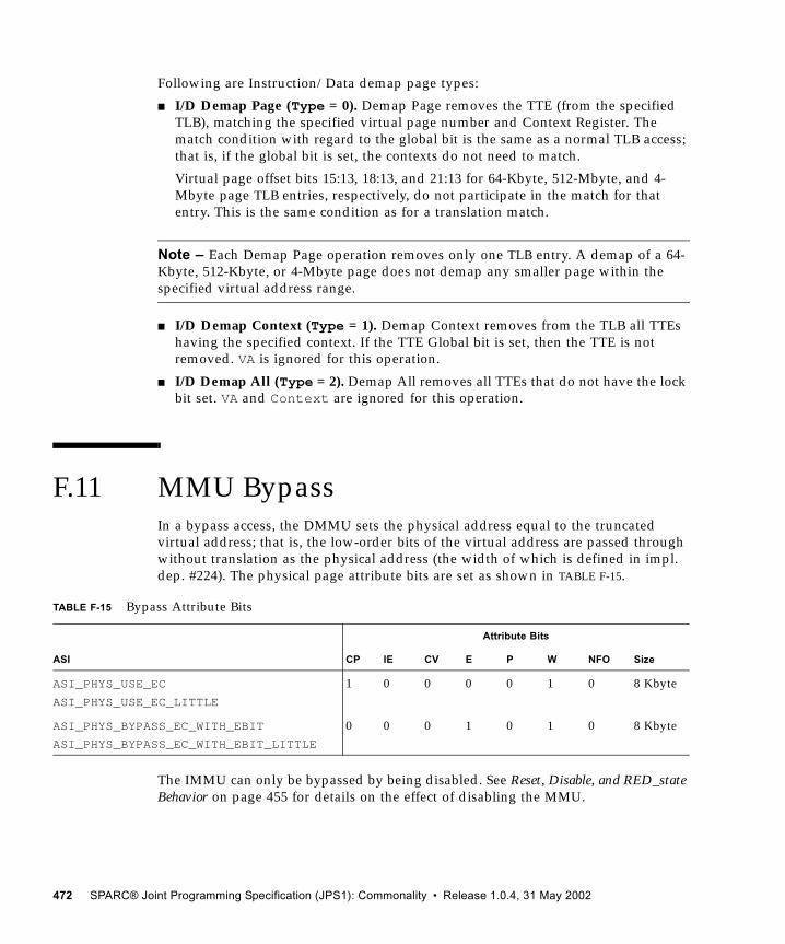
Following are Instruction/Data demap page types:
■ I/D Demap Page (Type = 0). Demap Page removes the TTE (from the specified TLB), matching the specified virtual page number and Context Register. The match condition with regard to the global bit is the same as a normal TLB access; that is, if the global bit is set, the contexts do not need to match.
Virtual page offset bits 15:13, 18:13, and 21:13 for 64-Kbyte, 512-Mbyte, and 4-Mbyte page TLB entries, respectively, do not participate in the match for that entry. This is the same condition as for a translation match.
Note – Each Demap Page operation removes only one TLB entry. A demap of a 64-Kbyte, 512-Kbyte, or 4-Mbyte page does not demap any smaller page within the specified virtual address range.
■ I/D Demap Context (Type = 1). Demap Context removes from the TLB all TTEs having the specified context. If the TTE Global bit is set, then the TTE is not removed. VA is ignored for this operation.
■ I/D Demap All (Type = 2). Demap All removes all TTEs that do not have the lock bit set. VA and Context are ignored for this operation.
F.11 MMU BypassIn a bypass access, the DMMU sets the physical address equal to the truncated virtual address; that is, the low-order bits of the virtual address are passed through without translation as the physical address (the width of which is defined in impl. dep. #224). The physical page attribute bits are set as shown in TABLE F-15.
The IMMU can only be bypassed by being disabled. See Reset, Disable, and RED_state Behavior on page 455 for details on the effect of disabling the MMU.
TABLE F-15 Bypass Attribute Bits
ASI
Attribute Bits
CP IE CV E P W NFO Size
ASI_PHYS_USE_EC
ASI_PHYS_USE_EC_LITTLE
1 0 0 0 0 1 0 8 Kbyte
ASI_PHYS_BYPASS_EC_WITH_EBIT
ASI_PHYS_BYPASS_EC_WITH_EBIT_LITTLE
0 0 0 1 0 1 0 8 Kbyte
472 SPARC® Joint Programming Specification (JPS1): Commonality • Release 1.0.4, 31 May 2002
Compatibility Note – The virtual address is wider than the physical address; thus, there is no need to use multiple ASIs to fill in the high-order physical address bits, as is done in SPARC V8 machines.
F.12 Translation Lookaside Buffer HardwareThis section briefly describes the TLB hardware. For more detailed information, refer to the Implementation Supplements or the corresponding microarchitecture specification.
F.12.1 TLB OperationsThe TLB supports exactly one of the following operations:
■ Normal translation. The TLB receives a virtual address and a context identifier as input and produces a physical address and page attributes as output.
■ Bypass. The TLB receives a virtual address as input and produces a physical address equal to the truncated virtual address and default page attributes as output.
■ Demap operation. The TLB receives a virtual address, a context identifier, and type as input and sets the Valid bit to zero for any matching page entries.
■ Read operation. The TLB reads either the Tag or Data portion of the specified entry. (Since the TLB entry is greater than 64 bits, the Tag and Data portions must be returned in separate reads. See I/D TLB Data In, Data Access, and Tag Read Registers on page 461.)
■ Write operation. The TLB simultaneously writes the Tag and Data portion of the specified entry or the entry given by the replacement policy described below.
■ No operation. The TLB performs no operation.
F.12.2 TLB Replacement PolicyOn an automatic replacement write to the TLB, the MMU picks the entry to write, based on an implement-dependent algorithm. Please refer to the Implementation Supplements for details of the TLB replacement algorithm.
Release 1.0.4, 31 May 2002 C. Appendix F • Memory Management Unit 473
F.12.3 TSB Pointer Logic Hardware DescriptionThe algorithm used to generate the I/D TSB pointer is implementation dependent. Please refer to the Implementation Supplements for details of the TSB pointer generation algorithm.
474 SPARC® Joint Programming Specification (JPS1): Commonality • Release 1.0.4, 31 May 2002
C.APPENDIX G
Assembly Language Syntax
This appendix supports Appendix A, Instruction Definitions. Each instruction description in Appendix A includes a table that describes the suggested assembly language format for that instruction. This appendix describes the notation used in those assembly language syntax descriptions and lists some synthetic instructions provided by the SPARC JPS1 assemblers for the convenience of assembly language programmers.
The appendix contains these sections:
■ Notation Used on page 475■ Syntax Design on page 483■ Synthetic Instructions on page 484
G.1 Notation UsedThe notations defined here are also used in the assembly language syntax descriptions in Appendix A, Instruction Definitions.
Items in typewriter font are literals to be written exactly as they appear. Items in italic font are metasymbols that are to be replaced by numeric or symbolic values in actual SPARC V9 assembly language code. For example, “imm_asi” would be replaced by a number in the range 0 to 255 (the value of the imm_asi bits in the binary instruction) or by a symbol bound to such a number.
Subscripts on metasymbols further identify the placement of the operand in the generated binary instruction. For example, regrs2 is a reg (register name) whose binary value will be placed in the rs2 field of the resulting instruction.
Release 1.0.4, 31 May 2002 C. Appendix G • Assembly Language Syntax 475
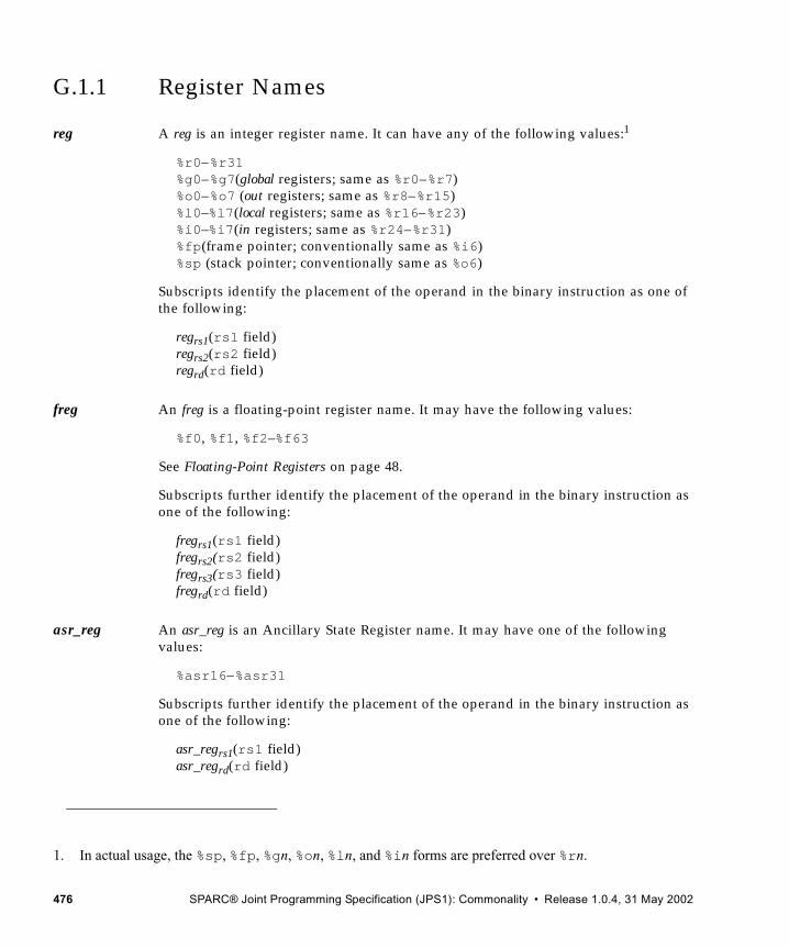
G.1.1 Register Names
reg A reg is an integer register name. It can have any of the following values:1
%r0–%r31%g0–%g7(global registers; same as %r0–%r7)%o0–%o7 (out registers; same as %r8–%r15)%l0–%l7(local registers; same as %r16–%r23)%i0–%i7(in registers; same as %r24–%r31)%fp(frame pointer; conventionally same as %i6)%sp (stack pointer; conventionally same as %o6)
Subscripts identify the placement of the operand in the binary instruction as one of the following:
regrs1(rs1 field)regrs2(rs2 field)regrd(rd field)
freg An freg is a floating-point register name. It may have the following values:
%f0, %f1, %f2–%f63
See Floating-Point Registers on page 48.
Subscripts further identify the placement of the operand in the binary instruction as one of the following:
fregrs1(rs1 field)fregrs2(rs2 field)fregrs3(rs3 field)fregrd(rd field)
asr_reg An asr_reg is an Ancillary State Register name. It may have one of the following values:
%asr16–%asr31
Subscripts further identify the placement of the operand in the binary instruction as one of the following:
asr_regrs1(rs1 field)asr_regrd(rd field)
1. In actual usage, the %sp, %fp, %gn, %on, %ln, and %in forms are preferred over %rn.
476 SPARC® Joint Programming Specification (JPS1): Commonality • Release 1.0.4, 31 May 2002
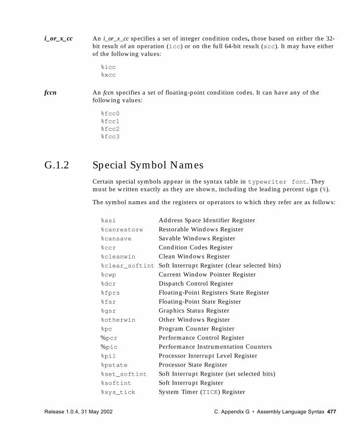
i_or_x_cc An i_or_x_cc specifies a set of integer condition codes, those based on either the 32-bit result of an operation (icc) or on the full 64-bit result (xcc). It may have either of the following values:
%icc%xcc
fccn An fccn specifies a set of floating-point condition codes. It can have any of the following values:
%fcc0%fcc1%fcc2%fcc3
G.1.2 Special Symbol NamesCertain special symbols appear in the syntax table in typewriter font. They must be written exactly as they are shown, including the leading percent sign (%).
The symbol names and the registers or operators to which they refer are as follows:
%asi Address Space Identifier Register%canrestore Restorable Windows Register%cansave Savable Windows Register%ccr Condition Codes Register%cleanwin Clean Windows Register%clear_softint Soft Interrupt Register (clear selected bits)%cwp Current Window Pointer Register%dcr Dispatch Control Register%fprs Floating-Point Registers State Register%fsr Floating-Point State Register%gsr Graphics Status Register%otherwin Other Windows Register%pc Program Counter Register%pcr Performance Control Register%pic Performance Instrumentation Counters%pil Processor Interrupt Level Register%pstate Processor State Register%set_softint Soft Interrupt Register (set selected bits)%softint Soft Interrupt Register%sys_tick System Timer (TICK) Register
Release 1.0.4, 31 May 2002 C. Appendix G • Assembly Language Syntax 477
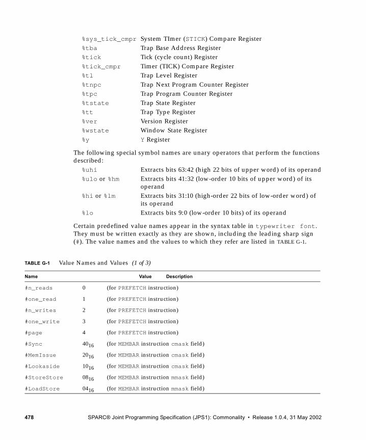
%sys_tick_cmpr System TImer (STICK) Compare Register%tba Trap Base Address Register%tick Tick (cycle count) Register%tick_cmpr Timer (TICK) Compare Register%tl Trap Level Register%tnpc Trap Next Program Counter Register%tpc Trap Program Counter Register%tstate Trap State Register%tt Trap Type Register%ver Version Register%wstate Window State Register%y Y Register
The following special symbol names are unary operators that perform the functions described:
%uhi Extracts bits 63:42 (high 22 bits of upper word) of its operand%ulo or %hm Extracts bits 41:32 (low-order 10 bits of upper word) of its
operand%hi or %lm Extracts bits 31:10 (high-order 22 bits of low-order word) of
its operand%lo Extracts bits 9:0 (low-order 10 bits) of its operand
Certain predefined value names appear in the syntax table in typewriter font. They must be written exactly as they are shown, including the leading sharp sign (#). The value names and the values to which they refer are listed in TABLE G-1.
TABLE G-1 Value Names and Values (1 of 3)
Name Value Description
#n_reads 0 (for PREFETCH instruction)
#one_read 1 (for PREFETCH instruction)
#n_writes 2 (for PREFETCH instruction)
#one_write 3 (for PREFETCH instruction)
#page 4 (for PREFETCH instruction)
#Sync 4016 (for MEMBAR instruction cmask field)
#MemIssue 2016 (for MEMBAR instruction cmask field)
#Lookaside 1016 (for MEMBAR instruction cmask field)
#StoreStore 0816 (for MEMBAR instruction mmask field)
#LoadStore 0416 (for MEMBAR instruction mmask field)
478 SPARC® Joint Programming Specification (JPS1): Commonality • Release 1.0.4, 31 May 2002
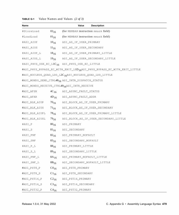
#StoreLoad 0216 (for MEMBAR instruction mmask field)
#LoadLoad 0116 (for MEMBAR instruction mmask field)
#ASI_AIUP 1016 ASI_AS_IF_USER_PRIMARY
#ASI_AIUS 1116 ASI_AS_IF_USER_SECONDARY
#ASI_AIUP_L 1816 ASI_AS_IF_USER_PRIMARY_LITTLE
#ASI_AIUS_L 1916 ASI_AS_IF_USER_SECONDARY_LITTLE
#ASI_PHYS_USE_EC_L1C16 ASI_PHYS_USE_EC_LITTLE
#ASI_PHYS_BYPASS_EC_WITH_EBIT_L1D16ASI_PHYS_BYPASS_EC_WITH_EBIT_LITTLE
#ASI_NUCLEUS_QUAD_LDD_L2C16ASI_NUCLEUS_QUAD_LDD_LITTLE
#ASI_MONDO_SEND_CTRL4816 ASI_INTR_DISPATCH_STATUS
#ASI_MONDO_RECEIVE_CTRL4916ASI_INTR_RECEIVE
#ASI_AFSR 4C16 ASI_ASYNC_FAULT_STATUS
#ASI_AFAR 4D16 ASI_ASYNC_FAULT_ADDR
#ASI_BLK_AIUP 7016 ASI_BLOCK_AS_IF_USER_PRIMARY
#ASI_BLK_AIUS 7116 ASI_BLOCK_AS_IF_USER_SECONDARY
#ASI_BLK_AIUPL 7816 ASI_BLOCK_AS_IF_USER_PRIMARY_LITTLE
#ASI_BLK_AIUSL 7916 ASI_BLOCK_AS_IF_USER_SECONDARY_LITTLE
#ASI_P 8016 ASI_PRIMARY
#ASI_S 8116 ASI_SECONDARY
#ASI_PNF 8216 ASI_PRIMARY_NOFAULT
#ASI_SNF 8316 ASI_SECONDARY_NOFAULT
#ASI_P_L 8816 ASI_PRIMARY_LITTLE
#ASI_S_L 8916 ASI_SECONDARY_LITTLE
#ASI_PNF_L 8A16 ASI_PRIMARY_NOFAULT_LITTLE
#ASI_SNF_L 8B16 ASI_SECONDARY_NOFAULT_LITTLE
#ASI_PST8_P C016 ASI_PST8_PRIMARY
#ASI_PST8_S C116 ASI_PST8_SECONDARY
#ASI_PST16_P C216 ASI_PST16_PRIMARY
#ASI_PST16_S C316 ASI_PST16_SECONDARY
#ASI_PST32_P C416 ASI_PST32_PRIMARY
TABLE G-1 Value Names and Values (2 of 3)
Name Value Description
Release 1.0.4, 31 May 2002 C. Appendix G • Assembly Language Syntax 479
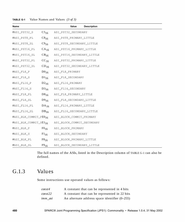
The full names of the ASIs, listed in the Description column of TABLE G-1 can also be defined.
G.1.3 ValuesSome instructions use operand values as follows:
const4 A constant that can be represented in 4 bits const22 A constant that can be represented in 22 bits imm_asi An alternate address space identifier (0–255)
#ASI_PST32_S C516 ASI_PST32_SECONDARY
#ASI_PST8_PL C816 ASI_PST8_PRIMARY_LITTLE
#ASI_PST8_SL C916 ASI_PST8_SECONDARY_LITTLE
#ASI_PST16_PL CA16 ASI_PST16_PRIMARY_LITTLE
#ASI_PST16_SL CB16 ASI_PST16_SECONDARY_LITTLE
#ASI_PST32_PL CC16 ASI_PST32_PRIMARY_LITTLE
#ASI_PST32_SL CD16 ASI_PST32_SECONDARY_LITTLE
#ASI_FL8_P D016 ASI_FL8_PRIMARY
#ASI_FL8_S D116 ASI_FL8_SECONDARY
#ASI_FL16_P D216 ASI_FL16_PRIMARY
#ASI_FL16_S D316 ASI_FL16_SECONDARY
#ASI_FL8_PL D816 ASI_FL8_PRIMARY_LITTLE
#ASI_FL8_SL D916 ASI_FL8_SECONDARY_LITTLE
#ASI_FL16_PL DA16 ASI_FL16_PRIMARY_LITTLE
#ASI_FL16_SL DB16 ASI_FL16_SECONDARY_LITTLE
#ASI_BLK_COMMIT_PE016 ASI_BLOCK_COMMIT_PRIMARY
#ASI_BLK_COMMIT_SE116 ASI_BLOCK_COMMIT_SECONDARY
#ASI_BLK_P F016 ASI_BLOCK_PRIMARY
#ASI_BLK_S F116 ASI_BLOCK_SECONDARY
#ASI_BLK_PL F816 ASI_BLOCK_PRIMARY_LITTLE
#ASI_BLK_SL F916 ASI_BLOCK_SECONDARY_LITTLE
TABLE G-1 Value Names and Values (3 of 3)
Name Value Description
480 SPARC® Joint Programming Specification (JPS1): Commonality • Release 1.0.4, 31 May 2002
simm7 A signed immediate constant that can be represented in 7 bits simm10 A signed immediate constant that can be represented in 10 bits simm11 A signed immediate constant that can be represented in 11 bits simm13 A signed immediate constant that can be represented in 13 bits value Any 64-bit valueshcnt32 A shift count from 0–31shcnt64 A shift count from 0–63
G.1.4 LabelsA label is a sequence of characters that comprises alphabetic letters (a–z, A–Z [with upper and lower case distinct]), underscores (_), dollar signs ($), periods (.), and decimal digits (0-9). A label may contain decimal digits, but it may not begin with one. A local label contains digits only.
G.1.5 Other Operand SyntaxSome instructions allow several operand syntaxes, as follows:
reg_plus_immCan be any of the following:
regrs1 (equivalent to regrs1 + %g0)regrs1 + simm13regrs1 – simm13simm13 (equivalent to %g0 + simm13)simm13 + regrs1 (equivalent to regrs1 + simm13)
address Can be any of the following: regrs1 (equivalent to regrs1 + %g0)regrs1 + simm13regrs1 – simm13simm13 (equivalent to %g0 + simm13)simm13 + regrs1 (equivalent to regrs1 + simm13)regrs1 + regrs2
Release 1.0.4, 31 May 2002 C. Appendix G • Assembly Language Syntax 481
membar_maskIs the following:
const7 — A constant that can be represented in 7 bits. Typically, this is an expression involving the logical OR of some combination of #Lookaside, #MemIssue, #Sync, #StoreStore, #LoadStore, #StoreLoad, and #LoadLoad.
prefetch_fcn (prefetch function)Can be any of the following:
#n_reads
#one_read
#n_writes
#one_write#page
0–31
regaddr (register-only address)Can be any of the following:
regrs1 (equivalent to regrs1 + %g0)regrs1 + regrs2
reg_or_imm (register or immediate value)Can be either of:
regrs2simm13
reg_or_imm10 (register or immediate value)Can be either of:
regrs2simm10
reg_or_imm11 (register or immediate value)Can be either of:
regrs2simm11
reg_or_shcnt (register or shift count value)Can be any of:
regrs2shcnt32
482 SPARC® Joint Programming Specification (JPS1): Commonality • Release 1.0.4, 31 May 2002
shcnt64
software_trap_numberCan be any of the following:
regrs1 (equivalent to regrs1 + %g0)regrs1 + simm7regrs1 – simm7simm7 (equivalent to %g0 + simm7)simm7 + regrs1 (equivalent to regrs1 + simm7)regrs1 + regrs2
The resulting operand value (software trap number) must be in the range 0–127, inclusive.
G.1.6 CommentsTwo types of comments are accepted by the SPARC V9 assembler: C-style “/*...*/” comments, which may span multiple lines, and “!...” comments, which extend from the “!” to the end of the line.
G.2 Syntax DesignThe SPARC V9 assembly language syntax is designed so that the following statements are true:
■ The destination operand (if any) is consistently specified as the last (rightmost) operand in an assembly language instruction.
■ A reference to the contents of a memory location (in a Load, Store, CASA, CASXA, LDSTUB(A), or SWAP(A) instruction) is always indicated by square brackets ( [] ); a reference to the address of a memory location (such as in a JMPL, CALL, or SETHI) is specified directly, without square brackets.
Release 1.0.4, 31 May 2002 C. Appendix G • Assembly Language Syntax 483
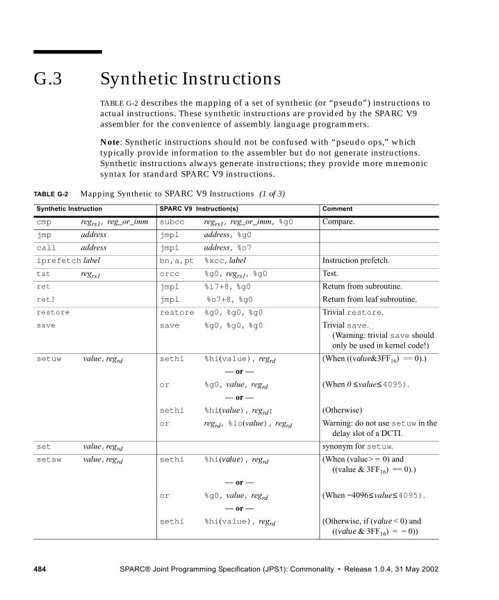
G.3 Synthetic Instructions TABLE G-2 describes the mapping of a set of synthetic (or “pseudo”) instructions to actual instructions. These synthetic instructions are provided by the SPARC V9 assembler for the convenience of assembly language programmers.
Note: Synthetic instructions should not be confused with “pseudo ops,” which typically provide information to the assembler but do not generate instructions. Synthetic instructions always generate instructions; they provide more mnemonic syntax for standard SPARC V9 instructions.
TABLE G-2 Mapping Synthetic to SPARC V9 Instructions (1 of 3)
Synthetic Instruction SPARC V9 Instruction(s) Comment
cmp regrs1, reg_or_imm subcc regrs1, reg_or_imm, %g0 Compare.
jmp address jmpl address, %g0
call address jmpl address, %o7
iprefetch label bn,a,pt %xcc,label Instruction prefetch.
tst regrs1 orcc %g0, regrs1, %g0 Test.
ret jmpl %i7+8, %g0 Return from subroutine.
retl jmpl %o7+8, %g0 Return from leaf subroutine.
restore restore %g0, %g0, %g0 Trivial restore.
save save %g0, %g0, %g0 Trivial save.(Warning: trivial save should only be used in kernel code!)
setuw value,regrd sethi %hi(value), regrd (When ((value&3FF16) == 0).)
— or —
or %g0, value, regrd (When 0 ≤value≤4095).
— or —
sethi %hi(value), regrd; (Otherwise)
or regrd, %lo(value), regrd Warning: do not use setuw in the delay slot of a DCTI.
set value,regrd synonym for setuw.
setsw value,regrd sethi %hi(value), regrd (When (value> = 0) and ((value & 3FF16) == 0).)
— or —
or %g0, value, regrd (When −4096≤value≤4095).
— or —
sethi %hi(value), regrd (Otherwise, if (value < 0) and ((value & 3FF16) = = 0))
484 SPARC® Joint Programming Specification (JPS1): Commonality • Release 1.0.4, 31 May 2002
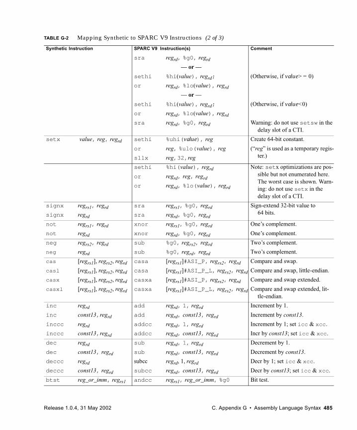
sra regrd, %g0, regrd
— or —
sethi %hi(value), regrd; (Otherwise, if value> = 0)
or regrd, %lo(value), regrd
— or —
sethi %hi(value), regrd; (Otherwise, if value<0)
or regrd, %lo(value), regrd
sra regrd, %g0, regrd Warning: do not use setsw in the delay slot of a CTI.
setx value, reg, regrd sethi %uhi(value), reg Create 64-bit constant.
or reg, %ulo(value), reg (“reg” is used as a temporary regis-ter.)sllx reg,32,reg
sethi %hi(value), regrd Note: setx optimizations are pos-sible but not enumerated here. The worst case is shown. Warn-ing: do not use setx in the delay slot of a CTI.
or regrd, reg, regrd
or regrd, %lo(value), regrd
signx regrs1, regrd sra regrs1, %g0, regrd Sign-extend 32-bit value to 64 bits.signx regrd sra regrd, %g0, regrd
not regrs1, regrd xnor regrs1, %g0, regrd One’s complement.
not regrd xnor regrd, %g0, regrd One’s complement.
neg regrs2, regrd sub %g0, regrs2, regrd Two’s complement.
neg regrd sub %g0, regrd, regrd Two’s complement.
cas [regrs1], regrs2, regrd casa [regrs1]#ASI_P, regrs2, regrd Compare and swap.
casl [regrs1], regrs2, regrd casa [regrs1]#ASI_P_L, regrs2, regrd Compare and swap, little-endian.
casx [regrs1], regrs2, regrd casxa [regrs1]#ASI_P, regrs2, regrd Compare and swap extended.
casxl [regrs1], regrs2, regrd casxa [regrs1]#ASI_P_L, regrs2, regrd Compare and swap extended, lit-tle-endian.
inc regrd add regrd, 1, regrd Increment by 1.
inc const13,regrd add regrd, const13, regrd Increment by const13.
inccc regrd addcc regrd, 1, regrd Increment by 1; set icc & xcc.
inccc const13,regrd addcc regrd, const13, regrd Incr by const13; set icc & xcc.
dec regrd sub regrd, 1, regrd Decrement by 1.
dec const13, regrd sub regrd, const13, regrd Decrement by const13.
deccc regrd subcc regrd, 1, regrd Decr by 1; set icc & xcc.
deccc const13, regrd subcc regrd, const13, regrd Decr by const13; set icc & xcc.
btst reg_or_imm, regrs1 andcc regrs1, reg_or_imm, %g0 Bit test.
TABLE G-2 Mapping Synthetic to SPARC V9 Instructions (2 of 3)
Synthetic Instruction SPARC V9 Instruction(s) Comment
Release 1.0.4, 31 May 2002 C. Appendix G • Assembly Language Syntax 485
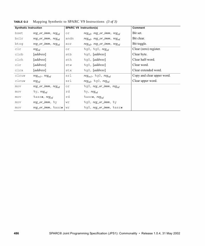
bset reg_or_imm, regrd or regrd, reg_or_imm, regrd Bit set.
bclr reg_or_imm, regrd andn regrd, reg_or_imm, regrd Bit clear.
btog reg_or_imm, regrd xor regrd, reg_or_imm, regrd Bit toggle.
clr regrd or %g0, %g0, regrd Clear (zero) register.
clrb [address] stb %g0, [address] Clear byte.
clrh [address] sth %g0, [address] Clear half-word.
clr [address] stw %g0, [address] Clear word.
clrx [address] stx %g0, [address] Clear extended word.
clruw regrs1, regrd srl regrs1, %g0, regrd Copy and clear upper word.
clruw regrd srl regrd, %g0, regrd Clear upper word.
mov reg_or_imm, regrd or %g0, reg_or_imm, regrd
mov %y, regrd rd %y, regrd
mov %asrn, regrd rd %asrn, regrd
mov reg_or_imm, %y wr %g0, reg_or_imm, %y
mov reg_or_imm, %asrn wr %g0, reg_or_imm, %asrn
TABLE G-2 Mapping Synthetic to SPARC V9 Instructions (3 of 3)
Synthetic Instruction SPARC V9 Instruction(s) Comment
486 SPARC® Joint Programming Specification (JPS1): Commonality • Release 1.0.4, 31 May 2002
C.APPENDIX H
Software Considerations
This appendix contains only material from The SPARC Architecture Manual, Version 9, and describes how software can use the SPARC V9 architecture effectively. Examples do not necessarily conform to any specific Application Binary Interface (ABI).
This appendix is informative only. It is not part of the SPARC V9 specification.
H.1 Nonprivileged SoftwareThis subsection describes software conventions that have proven or may prove useful, assumptions that compilers may make about the resources available, and how compilers can use those resources. It does not discuss how supervisor software (an operating system) may use the architecture. Although a set of software conventions is described, software is free to use other conventions more appropriate for specific applications.
The following are the primary goals for many of the software conventions described in this subsection:
■ Minimizing average procedure-call overhead■ Minimizing latency due to branches■ Minimizing latency due to memory access
H.1.1 RegistersRegister usage is a critical resource allocation issue for compilers. The SPARC V9 architecture provides windowed integer registers (in, out, local), global integer registers, and floating-point registers.
Release 1.0.4, 31 May 2002 C. Appendix H • Software Considerations 487
In and Out Registers
The in and out registers are used primarily for passing parameters to and receiving results from subroutines, and for keeping track of the memory stack. When a procedure is called and executes a SAVE instruction, the caller’s outs become the callee’s ins.
One of a procedure’s out registers (%o6) is used as its stack pointer, %sp. It points to an area in which the system can store %r16–%r31 (%l0–%l7 and %i0–%i7) when the register file overflows (spill trap), and is used to address most values located on the stack. A trap can occur at any time,1 which may precipitate a subsequent spill trap. During this spill trap, the contents of the user’s register window at the time of the original trap are spilled to the memory to which its %sp points.
A procedure may store temporary values in its out registers (except %sp) with the understanding that those values are volatile across procedure calls. %sp cannot be used for temporary values for the reasons described in Register Windows and %sp on page 489.
Up to six parameters2 may be passed by placing them in out registers %o0–%o5; additional parameters are passed in the memory stack. The stack pointer is implicitly passed in %o6, and a CALL instruction places its own address in %o7.3 Floating-point parameters may also be passed in floating-point registers.
After a callee is entered and its SAVE instruction has been executed, the caller’s out registers are accessible as the callee’s in registers.
The caller’s stack pointer %sp (%o6) automatically becomes the current procedure’s frame pointer %fp (%i6) when the SAVE instruction is executed.
The callee finds its first six integer parameters in %i0–%i5, and the remainder (if any) on the stack.
A function returns a scalar integer value by writing it into its ins (which are the caller’s outs), starting with %i0. A scalar floating-point value is returned in the floating-point registers, starting with %f0.
A procedure’s return address, normally the address of the instruction just after the CALL’s delay-slot instruction, is as %i7+8.4
1. For example, due to an error in executing an instruction (for example, a mem_address_not_aligned trap), or due to any type of external interrupt.
2. Six is more than adequate, since the overwhelming majority of procedures in system code take fewer than six parameters. According to studies cited by Weicker (Weicker, R. P., “Dhrystone: A Synthetic Systems Programming Benchmark,” CACM 27:10, October 1984), at least 97% (measured statically) take fewer than six parameters. The average number of parameters did not exceed 2.1, measured either statically or dynamically, in any of these studies.
3. If a JMPL instruction is used in place of a CALL, it should place its address in %o7 for consistency.
4. For convenience, SPARC V9 assemblers may provide a “ret” (return) synthetic instruction that generates a “jmpl %i7+8, %g0” hardware instruction. See G.3, Synthetic Instructions.
488 SPARC® Joint Programming Specification (JPS1): Commonality • Release 1.0.4, 31 May 2002

Local Registers
The locals are used for automatic1 variables and for most temporary values. For access efficiency, a compiler may also copy parameters (that is, those past the sixth) from the memory stack into the locals and use them from there.
See Register Allocation Within a Window on page 494 for methods of allocating more or fewer than eight registers for local values.
Register Windows and %sp
Some caveats about the use of %sp and the SAVE and RESTORE instructions are appropriate. If the operating system and user code use register windows, it is essential that
■ %sp always contains a correct value, so that when (and if) a register window spill/fill trap occurs, the register window can be correctly stored to or reloaded from memory.2
■ Nonprivileged code uses SAVE and RESTORE instructions carefully. In particular, “walking” the call chain through the register windows using RESTOREs, expecting to be able to return to where one started using SAVEs, does not work as one might suppose. Since user code cannot disable traps, a trap (e.g., an interrupt) could write over the contents of a user register window that has “temporarily” been RESTOREd.3 The safe method is to flush the register windows to user memory (the stack) with the FLUSHW instruction. Then, user code can safely walk the call chain through user memory, instead of through the register windows.
To avoid such problems, consider all data memory at addresses just less than %sp to be volatile, and the contents of all register windows “below” the current one to be volatile.
Global Registers
Unlike the ins, locals, and outs, the globals are not part of any register window. The globals are a set of eight registers with global scope, like the register sets of more traditional processor architectures. An ABI may define conventions that the globals (except %g0) must obey. For example, if the convention assumes that globals are volatile across procedure calls, either the caller or the callee must take responsibility for saving and restoring their contents.
1. In the C language, an automatic variable is a local variable whose lifetime is no longer than that of its containing procedure.
2. Typically, the SAVE instruction is used to generate a new %sp value while shifting to a new register window, all in one atomic operation. When SAVE is used this way, synchronization of the two operations should not be a problem.
3. Another reason this might fail is that user code has no way to determine how many register windows are implemented by the hardware.
Release 1.0.4, 31 May 2002 C. Appendix H • Software Considerations 489

Global register %g0 has a hardwired value of zero; it always reads as zero, and writes to it have no program-visible effect.
Typically, the global registers other than %g0 are used for temporaries, global variables, or global pointers — either user variables, or values maintained as part of the program’s execution environment. For example, one could use globals in the execution environment by establishing a convention that global scalars are addressed via offsets from a global base register. In the most general case, memory accessed at an arbitrary address requires six instructions; for example,
sethi %hh(address),tmpor tmp, %hm(address), tmpsllx tmp, 32, tmpsethi %lm(address), reg or reg, %lo(address), regld [reg+tmp], reg
Use of a global base register for frequently accessed global values would provide faster (single-instruction) access to 213 bytes of those values; for example,
ld [%gn+offset], reg
Additional global registers could be used to provide single-instruction access to correspondingly more global values.
Floating-Point Registers
There are 16 quad-precision floating-point registers. The registers can also be accessed as 32 double-precision registers. In addition, the first 8 quad registers can also be accessed as 32 single-precision registers. Floating-point registers are accessed with different instructions than the integer registers; their contents can be moved among themselves, and to or from memory. See Floating-Point Registers on page 48 for more information about floating-point register aliasing.
Like the global registers, the floating-point registers must be managed by software. Compilers use the floating-point registers for user variables and compiler temporaries, pass floating-point parameters, and return floating-point results in them.
The Memory Stack
A stack is maintained to hold automatic variables, temporary variables, and return information for each invocation of a procedure. When a procedure is called, a stack frame is allocated; it is released when the procedure returns. The use of a stack for this purpose allows simple and efficient implementation of recursive procedures.
490 SPARC® Joint Programming Specification (JPS1): Commonality • Release 1.0.4, 31 May 2002
Under certain conditions, optimization can allow a leaf procedure to use its caller’s stack frame instead of one of its own. In that case, the procedure allocates no space of its own for a stack frame. See Leaf-Procedure Optimization, below, for more information.
The stack pointer %sp must always maintain the alignment required by the operating system’s ABI. This is at least doubleword alignment, possibly with a constant offset to increase stack addressability using constant offset addressing.
H.1.2 Leaf-Procedure Optimization A leaf procedure is one that is a “leaf” in the program’s call graph; that is, one that does not call (e.g., via CALL or JMPL) any other procedures.
Each procedure, including leaf procedures, normally uses a SAVE instruction to allocate a stack frame and obtain a register window for itself, and a corresponding RESTORE instruction to deallocate it. The time costs associated with this are
■ Possible generation of register-window spill/fill traps at runtime. This only happens occasionally,1 but when either a spill or fill trap does occur, it costs several machine cycles to process.
■ The cycles expended by the SAVE and RESTORE instructions themselves.
There are also space costs associated with this convention, the cumulative cache effects of which may be nonnegligible. The space costs include
■ The space occupied on the stack by the procedure’s stack frame
■ The two words occupied by the SAVE and RESTORE instructions
Of the above costs, the trap-processing cycles typically are the most significant.
Some leaf procedures can be made to operate without their own register window or stack frame, using their caller’s instead. This can be done when the candidate leaf procedure meets all of the following conditions:2
■ It contains no references to %sp, except in its SAVE instruction.
■ It contains no references to %fp.
■ It refers to (or can be made to refer to) no more than 8 of the 32 integer registers, including %o7 (the return address).
If a procedure conforms to the above conditions, it can be made to operate using its caller’s stack frame and registers, an optimization that saves both time and space. This optimization is called leaf procedure optimization. The optimized procedure may
1. The frequency of overflow and underflow traps depends on the application and on the number of register windows (NWINDOWS) implemented in hardware.
2. Although slightly less restrictive conditions could be used, the optimization would become more complex to perform and the incremental gain would usually be small.
Release 1.0.4, 31 May 2002 C. Appendix H • Software Considerations 491
safely use only registers that its caller already assumes to be volatile across a procedure call.
The optimization can be performed at the assembly language level with the following steps:
1. Change all references to registers in the procedure to registers that the caller assumes volatile across the call.
a. Leave references to %o7 unchanged.
b. Leave any references to %g0–%g7 unchanged.
c. Change %i0–%i5 to %o0–%o5, respectively. If an in register is changed to an out register that was already referenced in the original unoptimized version of the procedure, all original references to that out register must be changed to refer to an unused out or global register.
d. Change references to each local register into references to any unused register that is assumed to be volatile across a procedure call.
2. Delete the SAVE instruction. If it was in a delay slot, replace it with a NOP instruction. If its destination register was not %g0 or %sp, convert the SAVE into the corresponding ADD instruction instead of deleting it.
3. If the RESTORE’s implicit addition operation is used for a productive purpose (such as setting the procedure’s return value), convert the RESTORE to the corresponding ADD instruction. Otherwise, the RESTORE is only used for stack and register-window deallocation; replace it with a NOP instruction (it is probably in the delay slot of the RET and so cannot be deleted).
4. Change the RET (return) synthetic instruction to RETL (return-from-leaf-procedure synthetic instruction).
5. Perform any optimizations newly made possible, such as combining instructions or filling the delay slot of the RETL (or the delay slot occupied by the SAVE) with a productive instruction.
After the above changes, there should be no SAVE or RESTORE instructions, and no references to in or local registers in the procedure body. All original references to ins are now to outs. All other register references are to registers that are assumed to be volatile across a procedure call.
Costs of optimizing leaf procedures in this way include
■ Additional intelligence in a peephole optimizer to recognize and optimize candidate leaf procedures
■ Additional intelligence in debuggers to properly report the call chain and the stack traceback for optimized leaf procedures1
492 SPARC® Joint Programming Specification (JPS1): Commonality • Release 1.0.4, 31 May 2002
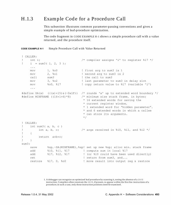
H.1.3 Example Code for a Procedure CallThis subsection illustrates common parameter-passing conventions and gives a simple example of leaf-procedure optimization.
The code fragment in CODE EXAMPLE H-1 shows a simple procedure call with a value returned, and the procedure itself.
1. A debugger can recognize an optimized leaf procedure by scanning it, noting the absence of a SAVE instruction. Compilers often constrain the SAVE, if present, to appear within the first few instructions of a procedure; in such a case, only those instruction positions need be examined.
! CALLER:! int i; /* compiler assigns "i" to register ! i = sum3( 1, 2, 3 );
...mov 1, %o0 ! first arg to sum3 is 1mov 2, %o1 ! second arg to sum3 is 2call sum3 ! the call to sum3mov 3, %o2 ! last parameter to sum3 in delay slmov %o0, %l7 ! copy return value to %l7 (variable...
#define SA(x) (((x)+15)&(~0x1F)) /* rounds "x" up to extended word bou*/#define MINFRAME ((16+1+6)*8) /* minimum size stack frame, in byte
* 16 extended words for saving the * current register window, * 1 extended word for “hidden param * and 6 extended words in which a c * can store its arguments. */
! CALLEE:! int sum3( a, b, c )! int a, b, c; /* args received in %i0, %i1, and %i! {! return a+b+c;! }sum3:
save %sp,-SA(MINFRAME),%sp! set up new %sp; alloc min. stack add %i0, %i1, %l7 ! compute sum in local %l7add %l7, %i2, %l7 ! (or %i0 could have been used direret ! return from sum3, and...restore %l7, 0, %o0 ! move result into output reg & res
CODE EXAMPLE H-1 Simple Procedure Call with Value Returned
! CALLER:! int i; /* compiler assigns "i" to register %l7 */! i = sum3( 1, 2, 3 );
...mov 1, %o0 ! first arg to sum3 is 1mov 2, %o1 ! second arg to sum3 is 2call sum3 ! the call to sum3mov 3, %o2 ! last parameter to sum3 in delay slotmov %o0, %l7 ! copy return value to %l7 (variable "i")...
#define SA(x) (((x)+15)&(~0x1F)) /* rounds "x" up to extended word boundary */#define MINFRAME ((16+1+6)*8) /* minimum size stack frame, in bytes;
* 16 extended words for saving the * current register window, * 1 extended word for “hidden parameter”, * and 6 extended words in which a callee * can store its arguments. */
! CALLEE:! int sum3( a, b, c )! int a, b, c; /* args received in %i0, %i1, and %i2 */! {! return a+b+c;! }sum3:
save %sp,-SA(MINFRAME),%sp! set up new %sp; alloc min. stack frameadd %i0, %i1, %l7 ! compute sum in local %l7add %l7, %i2, %l7 ! (or %i0 could have been used directly)ret ! return from sum3, and...restore %l7, 0, %o0 ! move result into output reg & restore
Release 1.0.4, 31 May 2002 C. Appendix H • Software Considerations 493
Since sum3 does not call any other procedures (i.e., it is a leaf procedure), it can be optimized to become:
sum3:add %o0, %o1, %o0retl ! (must use RETL, not RET,add %o0, %o2, %o0 ! to return from leaf procedure)
H.1.4 Register Allocation Within a Window The usual SPARC V9 software convention is to allocate eight registers (%l0–%l7) for local values. A compiler could allocate more registers for local values at the expense of having fewer outs and ins available for argument passing. For example, if instead of assuming that the boundary between local values and input arguments is between r[23] and r[24] (%l7 and %i0), software could, by convention, assume that the boundary is between r[25] and r[26] (%i1 and %i2). This would provide 10 registers for local values and 6 in and out registers. This is shown in TABLE H-1.
H.1.5 Other Register-Window-Usage Models So far, this appendix has described SPARC V9 software conventions that are appropriate for use in a general-purpose multitasking computer system. However, SPARC V9 is used in many other applications, notably embedded and/or real-time systems. In such applications, other schemes for allocation of SPARC V9’s register windows might be more nearly optimal than the one described above.
One possibility is to avoid using the normal register-window mechanism by not using SAVE and RESTORE instructions. Software would see 32 general-purpose registers instead of SPARC V9’s usual windowed register file. In this mode, SPARC V9 would operate like processors with more traditional (flat) register architectures. Procedure call times would be more determinate (due to lack of spill/fill traps), but for most types of software, average procedure call time would significantly increase,
TABLE H-1 Register Allocation Within a Window
Standard register model
10 local register model
Arbitrary register model
Registers for local values 8 10 n
In / out registers
Reserved for %sp / %fp 1 1 1
Reserved for return address 1 1 1
Available for argument passing 6 4 14 − n
Total ins / outs 8 6 16 − n
494 SPARC® Joint Programming Specification (JPS1): Commonality • Release 1.0.4, 31 May 2002
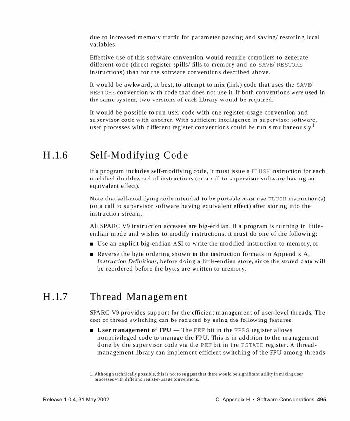
due to increased memory traffic for parameter passing and saving/restoring local variables.
Effective use of this software convention would require compilers to generate different code (direct register spills/fills to memory and no SAVE/RESTORE instructions) than for the software conventions described above.
It would be awkward, at best, to attempt to mix (link) code that uses the SAVE/RESTORE convention with code that does not use it. If both conventions were used in the same system, two versions of each library would be required.
It would be possible to run user code with one register-usage convention and supervisor code with another. With sufficient intelligence in supervisor software, user processes with different register conventions could be run simultaneously.1
H.1.6 Self-Modifying Code If a program includes self-modifying code, it must issue a FLUSH instruction for each modified doubleword of instructions (or a call to supervisor software having an equivalent effect).
Note that self-modifying code intended to be portable must use FLUSH instruction(s) (or a call to supervisor software having equivalent effect) after storing into the instruction stream.
All SPARC V9 instruction accesses are big-endian. If a program is running in little-endian mode and wishes to modify instructions, it must do one of the following:
■ Use an explicit big-endian ASI to write the modified instruction to memory, or
■ Reverse the byte ordering shown in the instruction formats in Appendix A, Instruction Definitions, before doing a little-endian store, since the stored data will be reordered before the bytes are written to memory.
H.1.7 Thread ManagementSPARC V9 provides support for the efficient management of user-level threads. The cost of thread switching can be reduced by using the following features:
■ User management of FPU — The FEF bit in the FPRS register allows nonprivileged code to manage the FPU. This is in addition to the management done by the supervisor code via the PEF bit in the PSTATE register. A thread-management library can implement efficient switching of the FPU among threads
1. Although technically possible, this is not to suggest that there would be significant utility in mixing user processes with differing register-usage conventions.
Release 1.0.4, 31 May 2002 C. Appendix H • Software Considerations 495
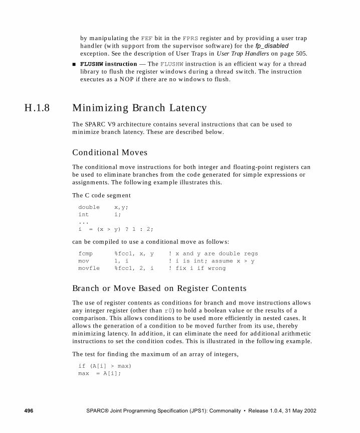
by manipulating the FEF bit in the FPRS register and by providing a user trap handler (with support from the supervisor software) for the fp_disabled exception. See the description of User Traps in User Trap Handlers on page 505.
■ FLUSHW instruction — The FLUSHW instruction is an efficient way for a thread library to flush the register windows during a thread switch. The instruction executes as a NOP if there are no windows to flush.
H.1.8 Minimizing Branch LatencyThe SPARC V9 architecture contains several instructions that can be used to minimize branch latency. These are described below.
Conditional Moves
The conditional move instructions for both integer and floating-point registers can be used to eliminate branches from the code generated for simple expressions or assignments. The following example illustrates this.
The C code segment
double x,y;int i;...i = (x > y) ? 1 : 2;
can be compiled to use a conditional move as follows:
fcmp %fcc1, x, y ! x and y are double regsmov 1, i ! i is int; assume x > ymovfle %fcc1, 2, i ! fix i if wrong
Branch or Move Based on Register Contents
The use of register contents as conditions for branch and move instructions allows any integer register (other than r0) to hold a boolean value or the results of a comparison. This allows conditions to be used more efficiently in nested cases. It allows the generation of a condition to be moved further from its use, thereby minimizing latency. In addition, it can eliminate the need for additional arithmetic instructions to set the condition codes. This is illustrated in the following example.
The test for finding the maximum of an array of integers,
if (A[i] > max)max = A[i];
496 SPARC® Joint Programming Specification (JPS1): Commonality • Release 1.0.4, 31 May 2002
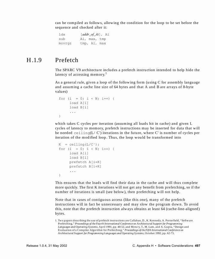
can be compiled as follows, allowing the condition for the loop to be set before the sequence and checked after it:
ldx [addr_of_Ai], Ai sub Ai, max, tmp movrgz tmp, Ai, max
H.1.9 PrefetchThe SPARC V9 architecture includes a prefetch instruction intended to help hide the latency of accessing memory.1
As a general rule, given a loop of the following form (using C for assembly language and assuming a cache line size of 64 bytes and that A and B are arrays of 8-byte values)
for (i = 0; i < N; i++) {load A[i]load B[i]...
}
which takes C cycles per iteration (assuming all loads hit in cache) and given L cycles of latency to memory, prefetch instructions may be inserted for data that will be needed ceiling(L/C') iterations in the future, where C' is number of cycles per iteration of the modified loop. Thus, the loop would be transformed into
K = ceiling(L/C');for (i = 0; i < N; i++) {
load A[i]load B[i]prefetch A[i+K]prefetch B[i+K]...
}
This ensures that the loads will find their data in the cache and will thus complete more quickly. The first K iterations will not get any benefit from prefetching, so if the number of iterations is small (see below), then prefetching will not help.
Note that in cases of contiguous access (like this one), many of the prefetch instructions will in fact be unnecessary and may slow the program down. To avoid this, note that the prefetch instruction always obtains at least 64 (cache-line-aligned) bytes.
1. Two papers describing the use of prefetch instructions are Callahan, D., K. Kennedy, A. Porterfield, “Software Prefetching,” Proceedings of the Fourth International Conference on Architectural Support for Programming Languages and Operating Systems, April 1991, pp. 40-52, and Mowry, T., M. Lam, and A. Gupta, “Design and Evaluation of a Compiler Algorithm for Prefetching,” Proceedings of the Fifth International Conference on Architectural Support for Programming Languages and Operating Systems, October 1992, pp. 62-73.
Release 1.0.4, 31 May 2002 C. Appendix H • Software Considerations 497
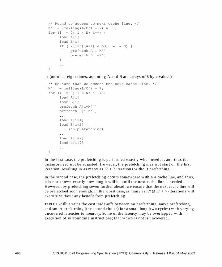
/* Round up access to next cache line. */K' = (ceiling(L/C') + 7) & ~7; for (i = 0; i < N; i++) {
load A[i]load B[i]if ( ((int)(A+i) & 63) = = 0) {
prefetch A[i+K']prefetch B[i+K']
}...
}
or (unrolled eight times, assuming A and B are arrays of 8-byte values)
/* Be sure that we access the next cache line. */K'' = ceiling(L/C') + 7;for (i = 0; i < N; i++) {
load A[i]load B[i]prefetch A[i+K'']prefetch B[i+K'']...load A[i+1]load B[i+2]... (no prefetching)...load A[i+7]load B[i+7]...
}
In the first case, the prefetching is performed exactly when needed, and thus the distance need not be adjusted. However, the prefetching may not start on the first iteration, resulting in as many as K' + 7 iterations without prefetching.
In the second case, the prefetching occurs somewhere within a cache line, and thus, it is not known exactly how long it will be until the next cache line is needed. However, by prefetching seven further ahead, we ensure that the next cache line will be prefetched soon enough. In the worst case, as many as K'' (≤ K' + 7) iterations will execute without any benefit from prefetching.
TABLE H-2 illustrates the cost trade-offs between no prefetching, naive prefetching, and smart prefetching (the second choice) for a small loop (two cycles) with varying uncovered latencies to memory. Some of the latency may be overlapped with execution of surrounding instructions; that which is not is uncovered.
498 SPARC® Joint Programming Specification (JPS1): Commonality • Release 1.0.4, 31 May 2002
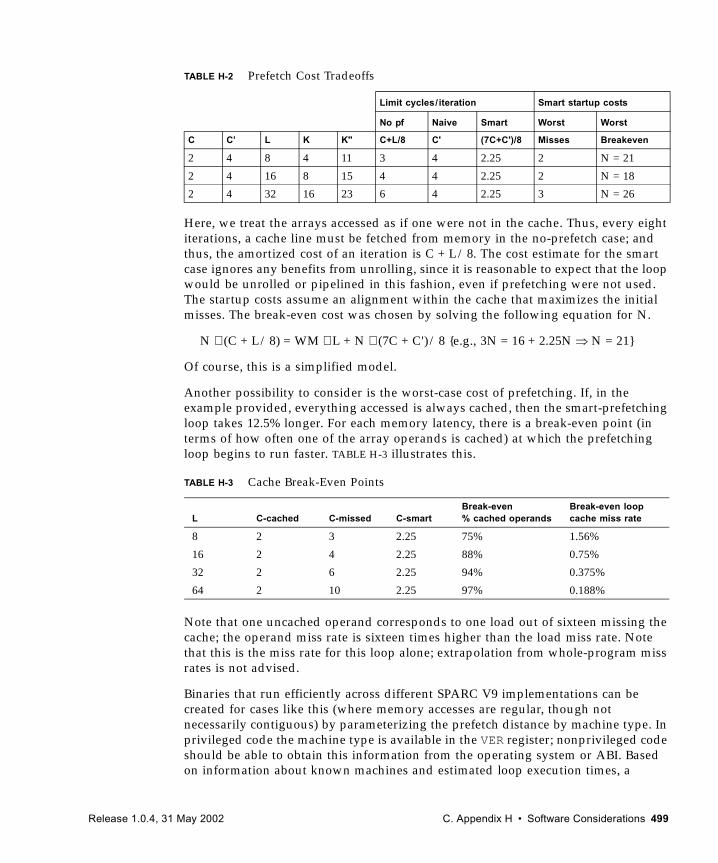
Here, we treat the arrays accessed as if one were not in the cache. Thus, every eight iterations, a cache line must be fetched from memory in the no-prefetch case; and thus, the amortized cost of an iteration is C + L/8. The cost estimate for the smart case ignores any benefits from unrolling, since it is reasonable to expect that the loop would be unrolled or pipelined in this fashion, even if prefetching were not used. The startup costs assume an alignment within the cache that maximizes the initial misses. The break-even cost was chosen by solving the following equation for N.
N ∗ (C + L/8) = WM ∗ L + N ∗ (7C + C')/8 {e.g., 3N = 16 + 2.25N ⇒ N = 21}
Of course, this is a simplified model.
Another possibility to consider is the worst-case cost of prefetching. If, in the example provided, everything accessed is always cached, then the smart-prefetching loop takes 12.5% longer. For each memory latency, there is a break-even point (in terms of how often one of the array operands is cached) at which the prefetching loop begins to run faster. TABLE H-3 illustrates this.
Note that one uncached operand corresponds to one load out of sixteen missing the cache; the operand miss rate is sixteen times higher than the load miss rate. Note that this is the miss rate for this loop alone; extrapolation from whole-program miss rates is not advised.
Binaries that run efficiently across different SPARC V9 implementations can be created for cases like this (where memory accesses are regular, though not necessarily contiguous) by parameterizing the prefetch distance by machine type. In privileged code the machine type is available in the VER register; nonprivileged code should be able to obtain this information from the operating system or ABI. Based on information about known machines and estimated loop execution times, a
TABLE H-2 Prefetch Cost Tradeoffs
Limit cycles/iteration Smart startup costs
No pf Naive Smart Worst Worst
C C’ L K K" C+L/8 C' (7C+C')/8 Misses Breakeven
2 4 8 4 11 3 4 2.25 2 N = 21
2 4 16 8 15 4 4 2.25 2 N = 18
2 4 32 16 23 6 4 2.25 3 N = 26
TABLE H-3 Cache Break-Even Points
L C-cached C-missed C-smartBreak-even% cached operands
Break-even loop cache miss rate
8 2 3 2.25 75% 1.56%
16 2 4 2.25 88% 0.75%
32 2 6 2.25 94% 0.375%
64 2 10 2.25 97% 0.188%
Release 1.0.4, 31 May 2002 C. Appendix H • Software Considerations 499
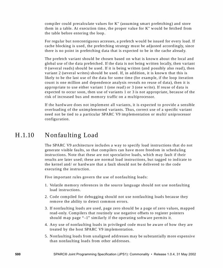
compiler could precalculate values for K'' (assuming smart prefetching) and store them in a table. At execution time, the proper value for K'' would be fetched from the table before entering the loop.
For regular but noncontiguous accesses, a prefetch would be issued for every load. If cache blocking is used, the prefetching strategy must be adjusted accordingly, since there is no point in prefetching data that is expected to be in the cache already.
The prefetch variant should be chosen based on what is known about the local and global use of the data prefetched. If the data is not being written locally, then variant 0 (several reads) should be used. If it is being written (and possibly also read), then variant 2 (several writes) should be used. If, in addition, it is known that this is likely to be the last use of the data for some time (for example, if the loop iteration count is one million and dependence analysis reveals no reuse of data), then it is appropriate to use either variant 1 (one read) or 3 (one write). If reuse of data is expected to occur soon, then use of variants 1 or 3 is not appropriate, because of the risk of increased bus and memory traffic on a multiprocessor.
If the hardware does not implement all variants, it is expected to provide a sensible overloading of the unimplemented variants. Thus, correct use of a specific variant need not be tied to a particular SPARC V9 implementation or multi/uniprocessor configuration.
H.1.10 Nonfaulting LoadThe SPARC V9 architecture includes a way to specify load instructions that do not generate visible faults, so that compilers can have more freedom in scheduling instructions. Note that these are not speculative loads, which may fault if their results are later used; these are normal load instructions, but tagged to indicate to the kernel and/or hardware that a fault should not be delivered to the code executing the instruction.
Five important rules govern the use of nonfaulting loads:
1. Volatile memory references in the source language should not use nonfaulting load instructions.
2. Code compiled for debugging should not use nonfaulting loads because they remove the ability to detect common errors.
3. If nonfaulting loads are used, page zero should be a page of zero values, mapped read-only. Compilers that routinely use negative offsets to register pointers should map page “–1” similarly if the operating software permits it.
4. Any use of nonfaulting loads in privileged code must be aware of how they are treated by the host SPARC V9 implementation.
5. Nonfaulting loads from unaligned addresses may be substantially more expensive than nonfaulting loads from other addresses.
500 SPARC® Joint Programming Specification (JPS1): Commonality • Release 1.0.4, 31 May 2002
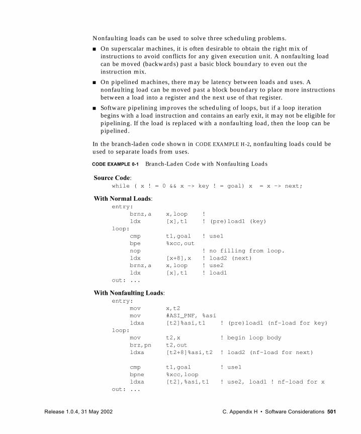
Nonfaulting loads can be used to solve three scheduling problems.
■ On superscalar machines, it is often desirable to obtain the right mix of instructions to avoid conflicts for any given execution unit. A nonfaulting load can be moved (backwards) past a basic block boundary to even out the instruction mix.
■ On pipelined machines, there may be latency between loads and uses. A nonfaulting load can be moved past a block boundary to place more instructions between a load into a register and the next use of that register.
■ Software pipelining improves the scheduling of loops, but if a loop iteration begins with a load instruction and contains an early exit, it may not be eligible for pipelining. If the load is replaced with a nonfaulting load, then the loop can be pipelined.
In the branch-laden code shown in CODE EXAMPLE H-2, nonfaulting loads could be used to separate loads from uses.
Source Code:while ( x ! = 0 && x -> key ! = goal) x = x -> next;
With Normal Loads:entry:
brnz,a x,loop ! ldx [x],t1 ! (pre)load1 (key)
loop:cmp t1,goal ! use1bpe %xcc,outnop ! no filling from loop.ldx [x+8],x ! load2 (next)brnz,a x,loop ! use2ldx [x],t1 ! load1
out: ...
With Nonfaulting Loads:entry:
mov x,t2mov #ASI_PNF, %asildxa [t2]%asi,t1 ! (pre)load1 (nf-load for key)
loop:mov t2,x ! begin loop body brz,pn t2,outldxa [t2+8]%asi,t2 ! load2 (nf-load for next)
cmp t1,goal ! use1 bpne %xcc,loopldxa [t2],%asi,t1 ! use2, load1 ! nf-load for x
out: ...
CODE EXAMPLE 0-1 Branch-Laden Code with Nonfaulting Loads
Release 1.0.4, 31 May 2002 C. Appendix H • Software Considerations 501
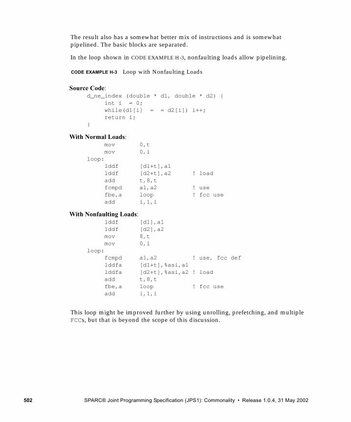
The result also has a somewhat better mix of instructions and is somewhat pipelined. The basic blocks are separated.
In the loop shown in CODE EXAMPLE H-3, nonfaulting loads allow pipelining.
This loop might be improved further by using unrolling, prefetching, and multiple FCCs, but that is beyond the scope of this discussion.
CODE EXAMPLE H-3 Loop with Nonfaulting Loads
Source Code:d_ne_index (double * d1, double * d2) {
int i = 0;while(d1[i] = = d2[i]) i++; return i;
}
With Normal Loads:mov 0,tmov 0,i
loop:lddf [d1+t],a1lddf [d2+t],a2 ! loadadd t,8,tfcmpd a1,a2 ! usefbe,a loop ! fcc useadd i,1,i
With Nonfaulting Loads:lddf [d1],a1lddf [d2],a2mov 8,tmov 0,i
loop:fcmpd a1,a2 ! use, fcc deflddfa [d1+t],%asi,a1lddfa [d2+t],%asi,a2 ! loadadd t,8,tfbe,a loop ! fcc useadd i,1,i
502 SPARC® Joint Programming Specification (JPS1): Commonality • Release 1.0.4, 31 May 2002
H.2 Supervisor SoftwareThis section discusses how supervisor software can use the SPARC V9 privileged architecture. It illustrates how the architecture can be used in an efficient manner. An implementation may choose to utilize different strategies based on its requirements and implementation-specific aspects of the architecture.
H.2.1 Trap HandlingThe SPARC V9 privileged architecture provides support for efficient trap handling, especially for window traps. The following features of the SPARC V9 privileged architecture can be used to write efficient trap handlers:
■ Multiple trap levels. The trap handlers for trap levels less than MAXTL – 1 can be written to ignore exceptional conditions and execute the common case efficiently (without checks and branches). For example, the fill/spill handlers can access pageable memory without first checking if it is resident. If the memory is not resident, the access will cause a trap that will be handled at the next trap level.
■ Vectoring of fill/spill traps. Supervisor software can set up the vectoring of fill/spill traps prior to executing code that uses register windows and may cause spill/fill traps. This feature can be used to support SPARC V8 and SPARC V7 binaries. These binaries create stack frames with save areas for 32-bit registers. SPARC V9 binaries create stack frames with save areas for 64-bit registers. By setting up the spill/fill trap vector based on the type of binary being executed, the trap handlers can avoid checking and branching to use the appropriate load/store instructions.
■ Saved trap state. Trap handlers need not save (restore) processor state that is automatically saved (restored) on a trap (return from trap). For example, the fill/spill trap handlers can load ASI_AS_IF_USER_PRIMARY{_LITTLE} into the ASI register in order to access the user’s address space without the overhead of having to save and restore the ASI register.
■ SAVED and RESTORED instructions. The SAVED (RESTORED) instruction provides an efficient way to update the state of the register windows after successfully spilling (filling) a register window. They implement a default policy of spilling (filling) one register window at a time. If desired, the supervisor software can implement a different policy by directly updating the state registers.
■ Alternate globals. The alternate global registers can be used to avoid saving and restoring the normal global registers. They can be used like the local registers of the trap window in SPARC V8.
■ Large trap vectors for spill/fill. The definition of the spill and fill trap vectors with reserved space between each pair of vectors allows spill and fill trap handlers to be up to 32 instructions long, thus avoiding a branch in the handler.
Release 1.0.4, 31 May 2002 C. Appendix H • Software Considerations 503
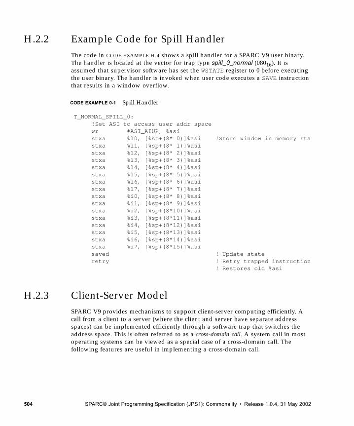
H.2.2 Example Code for Spill HandlerThe code in CODE EXAMPLE H-4 shows a spill handler for a SPARC V9 user binary. The handler is located at the vector for trap type spill_0_normal (08016). It is assumed that supervisor software has set the WSTATE register to 0 before executing the user binary. The handler is invoked when user code executes a SAVE instruction that results in a window overflow.
H.2.3 Client-Server ModelSPARC V9 provides mechanisms to support client-server computing efficiently. A call from a client to a server (where the client and server have separate address spaces) can be implemented efficiently through a software trap that switches the address space. This is often referred to as a cross-domain call. A system call in most operating systems can be viewed as a special case of a cross-domain call. The following features are useful in implementing a cross-domain call.
T_NORMAL_SPILL_0:!Set ASI to access user addr spacewr #ASI_AIUP, %asistxa %l0, [%sp+(8* 0)]%asi !Store window in memory stastxa %l1, [%sp+(8* 1)]%asistxa %l2, [%sp+(8* 2)]%asistxa %l3, [%sp+(8* 3)]%asistxa %l4, [%sp+(8* 4)]%asistxa %l5, [%sp+(8* 5)]%asistxa %l6, [%sp+(8* 6)]%asistxa %l7, [%sp+(8* 7)]%asistxa %i0, [%sp+(8* 8)]%asistxa %i1, [%sp+(8* 9)]%asistxa %i2, [%sp+(8*10)]%asistxa %i3, [%sp+(8*11)]%asistxa %i4, [%sp+(8*12)]%asistxa %i5, [%sp+(8*13)]%asistxa %i6, [%sp+(8*14)]%asistxa %i7, [%sp+(8*15)]%asisaved ! Update state retry ! Retry trapped instruction
! Restores old %asi
CODE EXAMPLE 0-1 Spill Handler
504 SPARC® Joint Programming Specification (JPS1): Commonality • Release 1.0.4, 31 May 2002
Splitting the Register Windows
The register windows can be shared efficiently between multiple address spaces by using the OTHERWIN register and providing additional trap handlers to handle spill/fill traps for the other (not the current) address spaces. On a cross-domain call (a software trap), the supervisor can set the OTHERWIN register to the number of register windows used by the client (equal to CANRESTORE) and CANRESTORE to zero. At the same time the WSTATE bit vectors can be set to vector the spill/fill traps appropriately for each address space.
The sequence in CODE EXAMPLE H-5 shows a cross-domain call and return. The example assumes the simple case, where only a single client-server pair can occupy the register windows. More general schemes can be developed along the same lines.
ASI_SECONDARY{_LITTLE}
Supervisor software can use these unrestricted ASIs to support cross-address-space access between clients and nonprivileged servers. For example, some services that are currently provided as part of a large monolithic supervisor can be separated out as nonprivileged servers (potentially occupying a separate address space). This is often referred to as the microkernel approach.
H.2.4 User Trap HandlersSupervisor software can provide efficient support for user (nonprivileged) trap handlers on SPARC V9. The RETURN instruction allows nonprivileged code to retry an instruction pointed to by the previous stack frame. This provides the semantics required for returning from a user trap handler without any change in processor state. Supervisor software can invoke the user trap handler by first creating a new register window (and stack frame) on its behalf and passing the necessary arguments (including the PC and nPC for the trapped instruction) in the local registers. The code in CODE EXAMPLE H-6 shows how a user trap handler may be invoked and how it returns.
Release 1.0.4, 31 May 2002 C. Appendix H • Software Considerations 505
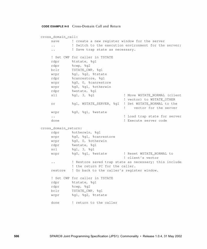
cross_domain_call:save ! create a new register window for the server.. ! Switch to the execution environment for the server;.. ! Save trap state as necessary.
! Set CWP for caller in TSTATErdpr %tstate, %g1rdpr %cwp, %g2bclr TSTATE_CWP, %g1wrpr %g1, %g2, %tstaterdpr %canrestore, %g1wrpr %g0, 0, %canrestorewrpr %g0, %g1, %otherwinrdpr %wstate, %g1sll %g1, 3, %g1 ! Move WSTATE_NORMAL (client
! vector) to WSTATE_OTHERor %g1, WSTATE_SERVER, %g1 ! Set WSTATE_NORMAL to the
! vector for the serverwrpr %g0, %g1, %wstate.. ! Load trap state for serverdone ! Execute server code
cross_domain_return:rdpr %otherwin, %g1wrpr %g0, %g1, %canrestorewrpr %g0, 0, %otherwinrdpr %wstate, %g1srl %g1, 3, %g1wrpr %g0, %g1, %wstate ! Reset WSTATE_NORMAL to
! client’s vector.. ! Restore saved trap state as necessary; this includes
! the return PC for the caller.restore ! Go back to the caller’s register window.
! Set CWP for caller in TSTATErdpr %tstate, %g1rdpr %cwp, %g2bclr TSTATE_CWP, %g1wrpr %g1, %g2, %tstate
done ! return to the caller
CODE EXAMPLE H-5 Cross-Domain Call and Return
506 SPARC® Joint Programming Specification (JPS1): Commonality • Release 1.0.4, 31 May 2002
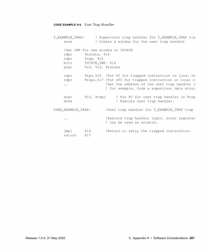
T_EXAMPLE_TRAP: ! Supervisor trap handler for T_EXAMPLE_TRAP trasave ! Create a window for the user trap handler
!Set CWP for new window in TSTATE rdpr %tstate, %l6rdpr %cwp, %l5bclr TSTATE_CWP, %l6wrpr %l6, %l5, %tstate
rdpr %tpc,%l6 !Put PC for trapped instruction in local rerdpr %tnpc,%l7 !Put nPC for trapped instruction in local re.. !Get the address of the user trap handler i
! for example, from a supervisor data struc
wrpr %l5, %tnpc ! Put PC for user trap handler in %tnpdone ! Execute user trap handler.
USER_EXAMPLE_TRAP: !User trap handler for T_EXAMPLE_TRAP trap
.. !Execute trap handler logic. Local register! can be used as scratch.
jmpl %l6 !Return to retry the trapped instruction.return %l7
CODE EXAMPLE H-6 User Trap Handler
Release 1.0.4, 31 May 2002 C. Appendix H • Software Considerations 507

508 SPARC® Joint Programming Specification (JPS1): Commonality • Release 1.0.4, 31 May 2002
C.APPENDIX I
Extending the SPARC V9 Architecture
This appendix contains only material from The SPARC Architecture Manual, Version 9 and describes how extensions can be effectively added to the SPARC V9 architecture. The appendix is informative only. It is not part of the SPARC V9 specification.
The appendix describes the two approved methods for adding new instructions: with read and write ancillary state register (ASR) and with implementation-dependent (IMPDEP2A) instructions. An implementor who wants to define and implement a new SPARC V9 instruction should, if possible, use one of those methods.
Caution – Programs that use SPARC V9 architectural extensions may not be portable and likely will not conform to any current or future SPARC V9 binary standards.
I.1 Read/Write Ancillary State Registers (ASRs)The first method of adding instructions to SPARC V9 is through the use of the implementation-dependent Write Ancillary State Register (WRASR) and Read Ancillary State Register (RDASR) instructions operating on ASRs 16–31. Through a read/write instruction pair, any instruction that requires an rs1, reg_or_imm, and rd field can be implemented. A WRASR instruction can also perform an arbitrary operation on two register sources, or on one register source and a signed immediate value, and place the result in an ASR. A subsequent RDASR instruction can read the result ASR and place its value in an integer destination register.
Release 1.0.4, 31 May 2002 C. Appendix I • Extending the SPARC V9 Architecture 509
I.2 Implementation-Dependent and Reserved OpcodesThe meaning of “reserved” for SPARC V9 opcodes differs from its meaning in SPARC V8. The SPARC V9 definition of “reserved” allows implementations to use reserved opcodes for implementation-specific purposes. While a hardware implementation that uses reserved opcodes will be SPARC V9-compliant, SPARC V9 ABI-compliant programs cannot use these reserved opcodes and remain compliant. A SPARC V9 platform that implements instructions using reserved opcodes must provide software libraries that provide the interface between SPARC V9 ABI-compliant programs and these instructions. Graphics libraries provide a good example of this. Hardware platforms have many diverse implementations of graphics acceleration hardware, but graphics application programs are insulated from this diversity through libraries.
There is no guarantee that a reserved opcode will not be used for additional instructions in a future version of the SPARC architecture. Implementors who use reserved opcodes should keep this fact in mind.
In some cases, forward compatibility may not be an issue; for example, in an embedded application, binary compatibility may not be an issue. These implementations can use any reserved opcodes for extensions.
Even when forward compatibility is an issue, future SPARC revisions are likely to contain few changes to opcode assignments, given that backward compatibility with previous versions must be maintained. It is recommended that implementations wishing to remain forward-compatible use the new IMPDEP2A reserved opcodes with op3<5:0> = 11 01112.
It is further recommended that SPARC International be notified of any use of IMPDEP2A or other reserved opcodes. When and if future revisions to SPARC are contemplated and if any SPARC V9 implementations have made use of reserved opcodes, SPARC International will make every effort not to use those opcodes. Coordinating through SPARC International provides feedback and cooperation in the choice of opcodes and maximizes the probability of forward compatibility. Given the historically small number of implementation-specific changes, coordinating through SPARC International should be sufficient to ensure future compatibility.
Note that SPARC JPS1 has already made use of many IMPDEP1 opcodes (see TABLE E-12 on page 435). Specific JPS1 implementations have used additional opcodes from IMPDEP1 and/or IMPDEP2; see individual JPS1 Implementation Supplements for details.
510 SPARC® Joint Programming Specification (JPS1): Commonality • Release 1.0.4, 31 May 2002
C.APPENDIX J
Programming with the Memory Models
This appendix contains only material from The SPARC Architecture Manual, Version 9, and describes how to program with the SPARC V9 memory models. An intuitive description of the models is provided in Chapter 8, Memory Models. A complete formal specification appears in Appendix D, Formal Specification of the Memory Models. In this appendix, general programming guidelines are given first, followed by specific examples showing how low-level synchronization can be implemented in TSO, PSO, and RMO.
Note that code written for a weaker memory model will execute correctly in any of the stronger memory models. Furthermore, the only possible difference between code written for a weaker memory model and the corresponding code for a stronger memory model is the presence of memory ordering instructions (MEMBARs) that are not needed for the stronger memory model. Hence, transforming code from/to a stronger memory model to/from a weaker memory model means adding/removing certain memory ordering instructions.1 The required memory ordering directives are monotonically ordered with respect to the strength of the memory model, with the weakest memory model requiring the strongest memory ordering instructions.
The code examples given below are written to run correctly using the RMO memory model. The comments on the MEMBAR instructions indicate which ordering constraints (if any) are required for the PSO and TSO memory models.
1. MEMBAR instructions specify seven independent ordering constraints; thus, there are cases where the transition to a stronger memory model allows the use of a less restrictive MEMBAR instruction but still requires a MEMBAR instruction. To demonstrate this property, the code examples given in this appendix use multiple MEMBAR instructions if some of the ordering constraints are needed in some but not all memory models. Multiple, adjacent MEMBAR instructions can always be replaced with a single MEMBAR instruction by ORing the arguments.
Release 1.0.4, 31 May 2002 C. Appendix J • Programming with the Memory Models 511
J.1 Memory Operations Programs access memory via five types of operations, namely, load, store, LDSTUB, SWAP, and compare-and-swap. Load copies a value from memory or an I/O location to a register. Store copies a value from a register into memory or an I/O location. LDSTUB, SWAP, and compare-and-swap are atomic load-store instructions that store a value into memory or an I/O location and return the old value in a register. The value written by the atomic instructions depends on the instruction. LDSTUB stores all ones in the accessed byte, SWAP stores the supplied value, and compare-and-swap stores the supplied value only if the old value equals the second supplied value.
Memory order and consistency are controlled by MEMBAR instructions. For example, a MEMBAR #StoreStore (equivalent to a STBAR in SPARC V8) ensures that all previous stores have been performed before subsequent stores and atomic load-stores are executed by memory. This particular memory order is guaranteed implicitly in TSO, but PSO and RMO require this instruction if the correctness of a program depends on the order in which two store instructions can be observed by another processor.
Note – Memory order is of concern only to programs containing multiple threads that share writable memory and that may run on multiple processors, and to those programs that reference I/O locations. Note that from the processor’s point of view, I/O devices behave like other processors
FLUSH is not a memory operation, but it is relevant here in the context of synchronizing stores with instruction execution. When a processor modifies an instruction at address A, it does a store to A followed by a FLUSH A. The FLUSH ensures that the change made by the store will become visible to the instruction fetch units of all processors in the system.
J.2 Memory Model SelectionGiven that all SPARC V9 systems are required to support TSO, programs written for any memory model will be able to run on any SPARC V9 system. However, a system running with the TSO model generally will offer lower performance than PSO or RMO because less concurrency is exposed to the CPU and the memory system. The motivation for weakening the memory model is to allow the CPU to issue multiple, concurrent memory references in order to hide memory latency and increase access bandwidth. For example, PSO and RMO allow the CPU to initiate new store operations before an outstanding store has completed.
512 SPARC® Joint Programming Specification (JPS1): Commonality • Release 1.0.4, 31 May 2002
Using a weaker memory model for an MP (multiprocessor) application that exhibits a high degree of read-write memory sharing with fine granularity and a high frequency of synchronization operations may result in frequent MEMBAR instructions.
In general, it is expected that the weaker memory models offer a performance advantage for multiprocessor SPARC V9 implementations.
J.3 Processors and Processes In the SPARC V9 memory models, the term “processor” may be replaced systematically by the term “process” or “thread,” as long as the code for switching processes or threads is written properly. The correct process-switch sequence is given in Process Switch Sequence on page 519. If an operating system implements this process-switch sequence, application programmers may completely ignore the difference between a process/thread and a processor.
J.4 Higher-Level Programming Languages and Memory ModelsThe SPARC V9 memory models are defined at the machine instruction level. Special attention is required to write the critical parts of MP/MT (multithreaded) applications in a higher-level language. Current higher-level languages do not support memory ordering instructions and atomic operations. As a result, MP/MT applications that are written in a higher-level language generally will rely on a library of MP/MT support functions, for example, the parmacs library from Argonne National Laboratory.1 The details of constructing and using such libraries are beyond the scope of this document.
Compiler optimizations such as code motion and instruction scheduling generally do not preserve the order in which memory is accessed, but they do preserve the data dependencies of a single thread. Compilers do not, in general, deal with the additional dependency requirements to support sharing read-write data among multiple concurrent threads. Hence, the memory semantics of a SPARC V9 system in general are not preserved by optimizing compilers. For this reason, and because memory ordering directives are not available from higher-level languages, the examples presented in this appendix use assembly language.
1. Lusk, E. L., R.A. Overbeek, “Use of Monitors in Fortran: A Tutorial on the Barrier, Self-scheduling Do-Loop, and Askfor Monitors,” TR# ANL-84-51, Argonne National Laboratory, June 1987.
Release 1.0.4, 31 May 2002 C. Appendix J • Programming with the Memory Models 513
Future compilers may have the ability to present the programmer with a sequentially consistent memory model despite the underlying hardware’s providing a weaker memory model.1
J.5 Portability and Recommended Programming Style Whether a program is portable across various memory models depends on how it synchronizes access to shared read-write data. Two aspects of a program’s style are relevant to portability:
■ Good semantics refers to whether the synchronization primitives chosen and the way in which they are used are such that changing the memory model does not involve making any changes to the code that uses the primitives.
■ Good structure refers to whether the code for synchronization is encapsulated through the use of primitives such that when the memory model is changed, required changes to the code are confined to the primitives.
Good semantics are a prerequisite for portability, and good structure makes porting easier.
Programs that use single-writer/multiple-reader locks to protect all access to shared read-write data are portable across all memory models. The code that implements the lock primitives themselves is portable across all models only if it is written to run correctly on RMO. If the lock primitives are collected into a library, then, at worst, only the library routines must be changed. Note that mutual exclusion (mutex) locks are a degenerate type of single-writer/multiple-readers lock.
Programs that use write locks to protect write accesses but read without locking are portable across all memory models only if writes to shared data are separated by MEMBAR #StoreStore instructions and if reading the lock is followed by a MEMBAR #LoadLoad instruction. If the MEMBAR instructions are omitted, the code is portable only across TSO and Strong Consistency,2 but generally it will not work with PSO and RMO. The code that implements the lock primitives is portable across all models only if it is written to run correctly on RMO. If the lock routines are collected into a library, the only possible changes not confined to the library routines are the MEMBAR instructions.
1. See Gharachorloo, K., S.V. Adve, A. Gupta, J.L. Hennessy, and M.D. Hill, “Programming for Different Memory Consistency Models,” Journal of Parallel and Distributed Systems, 15:4, August 1992.
2. Programs that assume a sequentially consistent memory are not guaranteed to run correctly on any SPARC V9-compliant system, since TSO is the strongest memory model required to be supported. However, sequential consistency is the most natural and intuitive programming model. This motivates the development of compiler techniques that allow programs written for sequential consistency to be translated into code that runs correctly (and efficiently) on systems with weaker memory models.
514 SPARC® Joint Programming Specification (JPS1): Commonality • Release 1.0.4, 31 May 2002
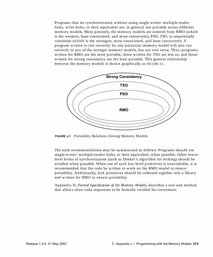
Programs that do synchronization without using single-writer/multiple-reader locks, write locks, or their equivalent are, in general, not portable across different memory models. More precisely, the memory models are ordered from RMO (which is the weakest, least constrained, and most concurrent), PSO, TSO, to sequentially consistent (which is the strongest, most constrained, and least concurrent). A program written to run correctly for any particular memory model will also run correctly in any of the stronger memory models, but not vice versa. Thus, programs written for RMO are the most portable, those written for TSO are less so, and those written for strong consistency are the least portable. This general relationship between the memory models is shown graphically in FIGURE J-1.
The style recommendations may be summarized as follows: Programs should use single-writer/multiple-reader locks, or their equivalent, when possible. Other lower-level forms of synchronization (such as Dekker’s algorithm for locking) should be avoided when possible. When use of such low-level primitives is unavoidable, it is recommended that the code be written to work on the RMO model to ensure portability. Additionally, lock primitives should be collected together into a library and written for RMO to ensure portability.
Appendix D, Formal Specification of the Memory Models, describes a tool and method that allows short code sequences to be formally verified for correctness.
Strong Consistency
TSO
PSO
RMO
FIGURE J-1 Portability Relations Among Memory Models
Release 1.0.4, 31 May 2002 C. Appendix J • Programming with the Memory Models 515
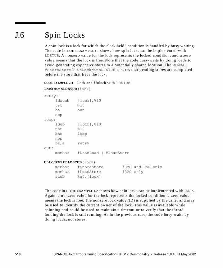
J.6 Spin Locks A spin lock is a lock for which the “lock held” condition is handled by busy waiting. The code in CODE EXAMPLE J-1 shows how spin locks can be implemented with LDSTUB. A nonzero value for the lock represents the locked condition, and a zero value means that the lock is free. Note that the code busy-waits by doing loads to avoid generating expensive stores to a potentially shared location. The MEMBAR #StoreStore in UnLockWithLDSTUB ensures that pending stores are completed before the store that frees the lock.
The code in CODE EXAMPLE J-2 shows how spin locks can be implemented with CASA. Again, a nonzero value for the lock represents the locked condition; a zero value means the lock is free. The nonzero lock value (ID) is supplied by the caller and may be used to identify the current owner of the lock. This value is available while spinning and could be used to maintain a timeout or to verify that the thread holding the lock is still running. As in the previous case, the code busy-waits by doing loads, not stores.
CODE EXAMPLE J-1 Lock and Unlock with LDSTUB
LockWithLDSTUB(lock)
retry:ldstub [lock],%l0tst %l0be outnop
loop:ldub [lock],%l0tst %l0bne loopnopba,a retry
out:membar #LoadLoad | #LoadStore
UnLockWithLDSTUB(lock)membar #StoreStore !RMO and PSO onlymembar #LoadStore !RMO onlystub %g0,[lock]
516 SPARC® Joint Programming Specification (JPS1): Commonality • Release 1.0.4, 31 May 2002
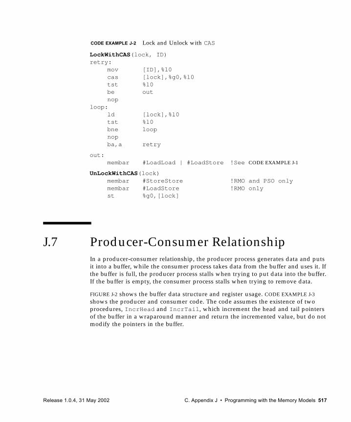
J.7 Producer-Consumer Relationship In a producer-consumer relationship, the producer process generates data and puts it into a buffer, while the consumer process takes data from the buffer and uses it. If the buffer is full, the producer process stalls when trying to put data into the buffer. If the buffer is empty, the consumer process stalls when trying to remove data.
FIGURE J-2 shows the buffer data structure and register usage. CODE EXAMPLE J-3 shows the producer and consumer code. The code assumes the existence of two procedures, IncrHead and IncrTail, which increment the head and tail pointers of the buffer in a wraparound manner and return the incremented value, but do not modify the pointers in the buffer.
LockWithCAS(lock, ID) retry:
mov [ID],%l0cas [lock],%g0,%l0tst %l0be outnop
loop:ld [lock],%l0tst %l0bne loopnopba,a retry
out:membar #LoadLoad | #LoadStore !See CODE EXAMPLE J-1
UnLockWithCAS(lock)membar #StoreStore !RMO and PSO onlymembar #LoadStore !RMO onlyst %g0,[lock]
CODE EXAMPLE J-2 Lock and Unlock with CAS
Release 1.0.4, 31 May 2002 C. Appendix J • Programming with the Memory Models 517
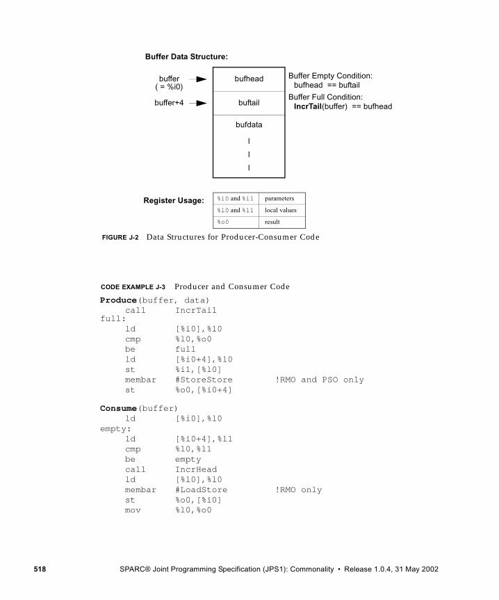
bufhead
buftail
bufdata
l
l
l
buffer Buffer Empty Condition:bufhead == buftail
Buffer Full Condition:IncrTail(buffer) == bufheadbuffer+4
( = %i0)
Buffer Data Structure:
Register Usage: %i0 and %i1
%o0
%l0 and %l1
parameters
local values
result
FIGURE J-2 Data Structures for Producer-Consumer Code
Produce(buffer, data)call IncrTail
full:ld [%i0],%l0cmp %l0,%o0be fullld [%i0+4],%l0st %i1,[%l0]membar #StoreStore !RMO and PSO onlyst %o0,[%i0+4]
Consume(buffer)ld [%i0],%l0
empty:ld [%i0+4],%l1cmp %l0,%l1be emptycall IncrHeadld [%l0],%l0membar #LoadStore !RMO onlyst %o0,[%i0]mov %l0,%o0
CODE EXAMPLE J-3 Producer and Consumer Code
518 SPARC® Joint Programming Specification (JPS1): Commonality • Release 1.0.4, 31 May 2002
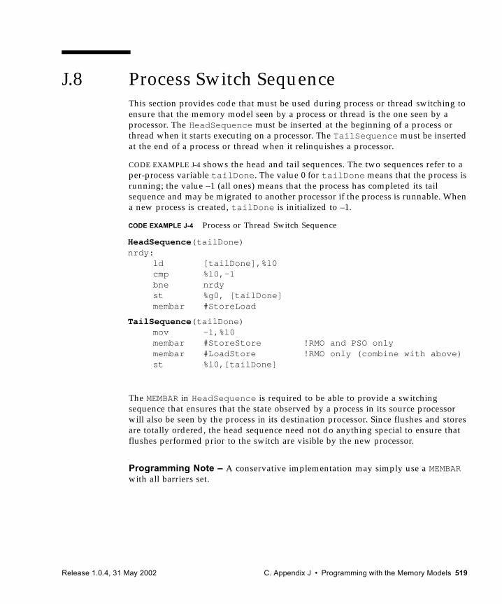
J.8 Process Switch Sequence This section provides code that must be used during process or thread switching to ensure that the memory model seen by a process or thread is the one seen by a processor. The HeadSequence must be inserted at the beginning of a process or thread when it starts executing on a processor. The TailSequence must be inserted at the end of a process or thread when it relinquishes a processor.
CODE EXAMPLE J-4 shows the head and tail sequences. The two sequences refer to a per-process variable tailDone. The value 0 for tailDone means that the process is running; the value –1 (all ones) means that the process has completed its tail sequence and may be migrated to another processor if the process is runnable. When a new process is created, tailDone is initialized to –1.
The MEMBAR in HeadSequence is required to be able to provide a switching sequence that ensures that the state observed by a process in its source processor will also be seen by the process in its destination processor. Since flushes and stores are totally ordered, the head sequence need not do anything special to ensure that flushes performed prior to the switch are visible by the new processor.
Programming Note – A conservative implementation may simply use a MEMBAR with all barriers set.
HeadSequence(tailDone)nrdy:
ld [tailDone],%l0cmp %l0,-1bne nrdyst %g0, [tailDone]membar #StoreLoad
TailSequence(tailDone)mov -1,%l0membar #StoreStore !RMO and PSO onlymembar #LoadStore !RMO only (combine with above)st %l0,[tailDone]
CODE EXAMPLE J-4 Process or Thread Switch Sequence
Release 1.0.4, 31 May 2002 C. Appendix J • Programming with the Memory Models 519
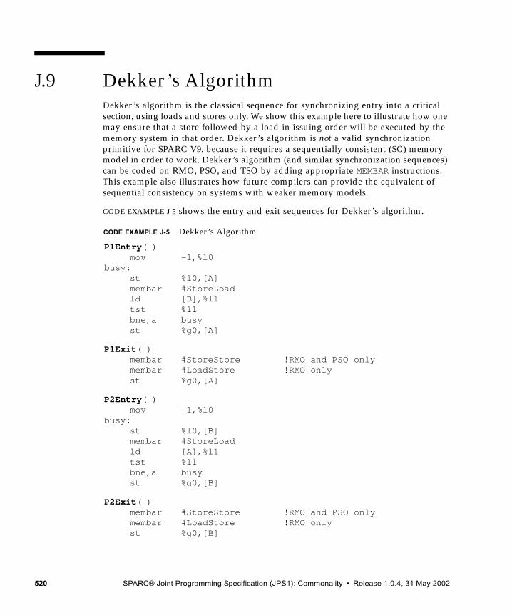
J.9 Dekker’s Algorithm Dekker’s algorithm is the classical sequence for synchronizing entry into a critical section, using loads and stores only. We show this example here to illustrate how one may ensure that a store followed by a load in issuing order will be executed by the memory system in that order. Dekker’s algorithm is not a valid synchronization primitive for SPARC V9, because it requires a sequentially consistent (SC) memory model in order to work. Dekker’s algorithm (and similar synchronization sequences) can be coded on RMO, PSO, and TSO by adding appropriate MEMBAR instructions. This example also illustrates how future compilers can provide the equivalent of sequential consistency on systems with weaker memory models.
CODE EXAMPLE J-5 shows the entry and exit sequences for Dekker’s algorithm.
P1Entry( )mov -1,%l0
busy:st %l0,[A]membar #StoreLoadld [B],%l1tst %l1bne,a busyst %g0,[A]
P1Exit( )membar #StoreStore !RMO and PSO onlymembar #LoadStore !RMO onlyst %g0,[A]
P2Entry( )mov -1,%l0
busy:st %l0,[B]membar #StoreLoadld [A],%l1tst %l1bne,a busyst %g0,[B]
P2Exit( )membar #StoreStore !RMO and PSO onlymembar #LoadStore !RMO onlyst %g0,[B]
CODE EXAMPLE J-5 Dekker’s Algorithm
520 SPARC® Joint Programming Specification (JPS1): Commonality • Release 1.0.4, 31 May 2002
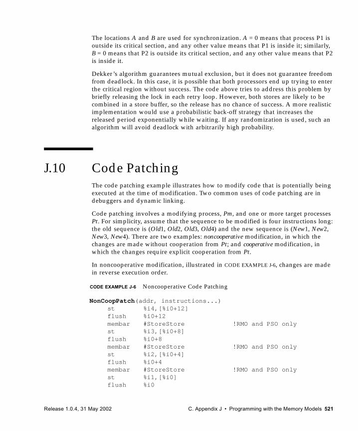
The locations A and B are used for synchronization. A = 0 means that process P1 is outside its critical section, and any other value means that P1 is inside it; similarly, B = 0 means that P2 is outside its critical section, and any other value means that P2 is inside it.
Dekker’s algorithm guarantees mutual exclusion, but it does not guarantee freedom from deadlock. In this case, it is possible that both processors end up trying to enter the critical region without success. The code above tries to address this problem by briefly releasing the lock in each retry loop. However, both stores are likely to be combined in a store buffer, so the release has no chance of success. A more realistic implementation would use a probabilistic back-off strategy that increases the released period exponentially while waiting. If any randomization is used, such an algorithm will avoid deadlock with arbitrarily high probability.
J.10 Code Patching The code patching example illustrates how to modify code that is potentially being executed at the time of modification. Two common uses of code patching are in debuggers and dynamic linking.
Code patching involves a modifying process, Pm, and one or more target processes Pt. For simplicity, assume that the sequence to be modified is four instructions long: the old sequence is (Old1, Old2, Old3, Old4) and the new sequence is (New1, New2, New3, New4). There are two examples: noncooperative modification, in which the changes are made without cooperation from Pt; and cooperative modification, in which the changes require explicit cooperation from Pt.
In noncooperative modification, illustrated in CODE EXAMPLE J-6, changes are made in reverse execution order.
NonCoopPatch(addr, instructions...)st %i4,[%i0+12]flush %i0+12membar #StoreStore !RMO and PSO onlyst %i3,[%i0+8]flush %i0+8membar #StoreStore !RMO and PSO onlyst %i2,[%i0+4]flush %i0+4membar #StoreStore !RMO and PSO onlyst %i1,[%i0] flush %i0
CODE EXAMPLE J-6 Noncooperative Code Patching
Release 1.0.4, 31 May 2002 C. Appendix J • Programming with the Memory Models 521
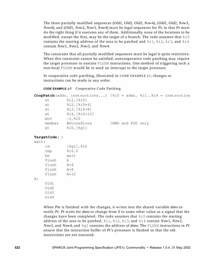
The three partially modified sequences (Old1, Old2, Old3, New4), (Old1, Old2, New3, New4), and (Old1, New2, New3, New4) must be legal sequences for Pt, in that Pt must do the right thing if it executes any of them. Additionally, none of the locations to be modified, except the first, may be the target of a branch. The code assumes that %i0 contains the starting address of the area to be patched and %i1, %i2, %i3, and %i4 contain New1, New2, New3, and New4.
The constraint that all partially modified sequences must be legal is quite restrictive. When this constraint cannot be satisfied, noncooperative code patching may require the target processor to execute FLUSH instructions. One method of triggering such a non-local FLUSH would be to send an interrupt to the target processor.
In cooperative code patching, illustrated in CODE EXAMPLE J-7, changes to instructions can be made in any order.
When Pm is finished with the changes, it writes into the shared variable done to notify Pt. Pt waits for done to change from 0 to some other value as a signal that the changes have been completed. The code assumes that %i0 contains the starting address of the area to be patched, %i1, %i2, %i3, and %i4 contain New1, New2, New3, and New4, and %g1 contains the address of done. The FLUSH instructions in Pt ensure that the instruction buffer of Pt’s processor is flushed so that the old instructions are not executed.
CoopPatch(addr, instructions...) !%i0 = addr, %i1..%i4 = instructionsst %i1,[%i0]st %i2,[%i0+4]st %i3,[%i0+8]st %i4,[%i0+12]mov -1,%l0membar #StoreStore !RMO and PSO onlyst %l0,[%g1]
TargetCode( )wait:
ld [%g1],%l0cmp %l0,0be waitflush Aflush A+4flush A+8flush A+12
A:Old1Old2Old3Old4
CODE EXAMPLE J-7 Cooperative Code Patching
522 SPARC® Joint Programming Specification (JPS1): Commonality • Release 1.0.4, 31 May 2002
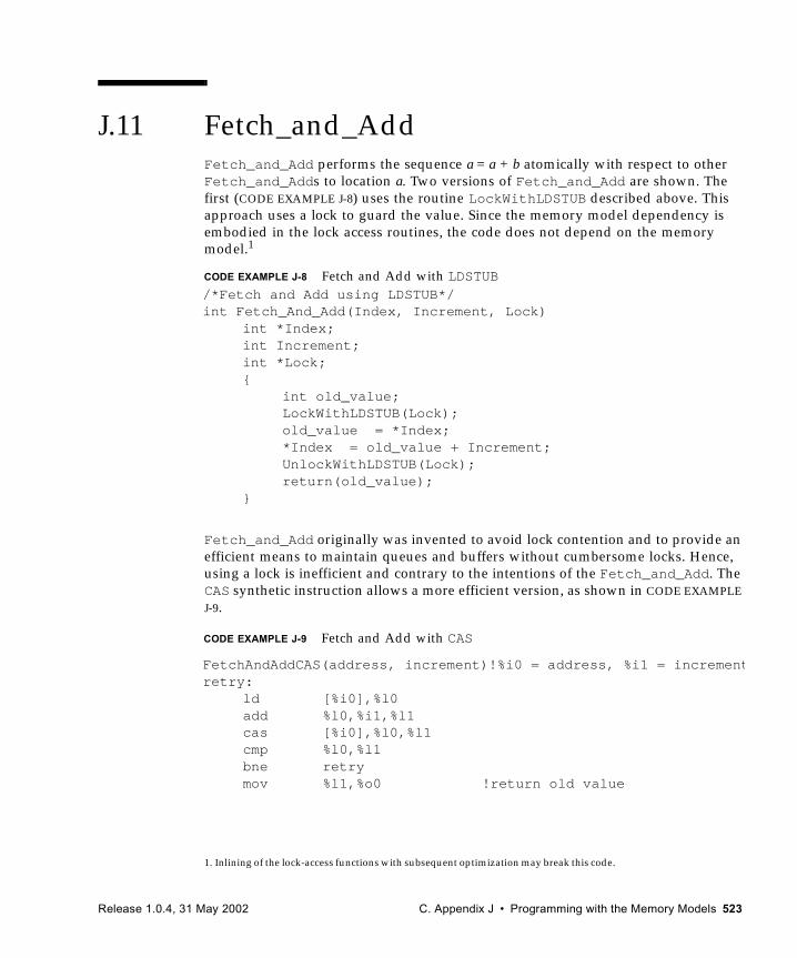
J.11 Fetch_and_Add Fetch_and_Add performs the sequence a = a + b atomically with respect to other Fetch_and_Adds to location a. Two versions of Fetch_and_Add are shown. The first (CODE EXAMPLE J-8) uses the routine LockWithLDSTUB described above. This approach uses a lock to guard the value. Since the memory model dependency is embodied in the lock access routines, the code does not depend on the memory model.1
Fetch_and_Add originally was invented to avoid lock contention and to provide an efficient means to maintain queues and buffers without cumbersome locks. Hence, using a lock is inefficient and contrary to the intentions of the Fetch_and_Add. The CAS synthetic instruction allows a more efficient version, as shown in CODE EXAMPLE J-9.
1. Inlining of the lock-access functions with subsequent optimization may break this code.
/*Fetch and Add using LDSTUB*/ int Fetch_And_Add(Index, Increment, Lock)
int *Index; int Increment; int *Lock; {
int old_value; LockWithLDSTUB(Lock); old_value = *Index; *Index = old_value + Increment; UnlockWithLDSTUB(Lock); return(old_value);
}
CODE EXAMPLE J-8 Fetch and Add with LDSTUB
FetchAndAddCAS(address, increment)!%i0 = address, %i1 = incrementretry:
ld [%i0],%l0add %l0,%i1,%l1cas [%i0],%l0,%l1cmp %l0,%l1bne retrymov %l1,%o0 !return old value
CODE EXAMPLE J-9 Fetch and Add with CAS
Release 1.0.4, 31 May 2002 C. Appendix J • Programming with the Memory Models 523
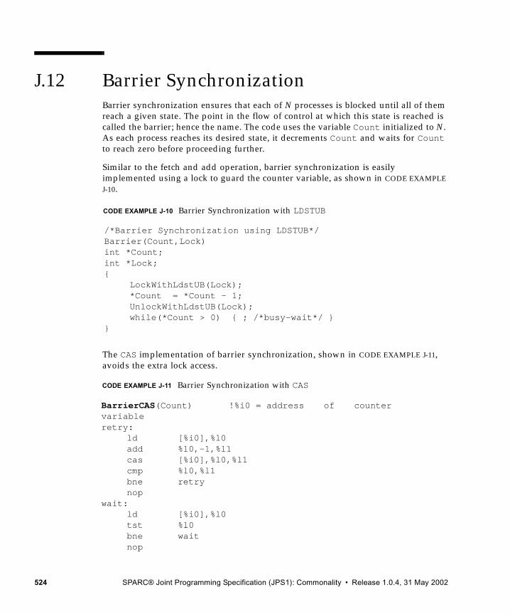
J.12 Barrier Synchronization Barrier synchronization ensures that each of N processes is blocked until all of them reach a given state. The point in the flow of control at which this state is reached is called the barrier; hence the name. The code uses the variable Count initialized to N. As each process reaches its desired state, it decrements Count and waits for Count to reach zero before proceeding further.
Similar to the fetch and add operation, barrier synchronization is easily implemented using a lock to guard the counter variable, as shown in CODE EXAMPLE J-10.
The CAS implementation of barrier synchronization, shown in CODE EXAMPLE J-11, avoids the extra lock access.
/*Barrier Synchronization using LDSTUB*/ Barrier(Count,Lock) int *Count; int *Lock; {
LockWithLdstUB(Lock); *Count = *Count - 1; UnlockWithLdstUB(Lock); while(*Count > 0) { ; /*busy-wait*/ }
}
CODE EXAMPLE J-10 Barrier Synchronization with LDSTUB
BarrierCAS(Count) !%i0 = address of countervariableretry:
ld [%i0],%l0add %l0,-1,%l1cas [%i0],%l0,%l1cmp %l0,%l1bne retrynop
wait:ld [%i0],%l0tst %l0bne waitnop
CODE EXAMPLE J-11 Barrier Synchronization with CAS
524 SPARC® Joint Programming Specification (JPS1): Commonality • Release 1.0.4, 31 May 2002
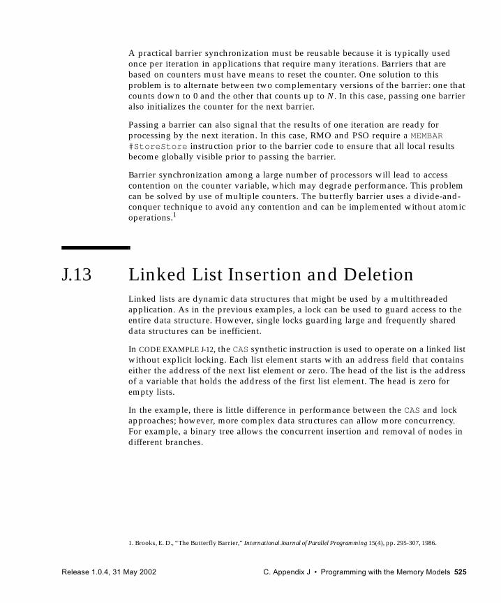
A practical barrier synchronization must be reusable because it is typically used once per iteration in applications that require many iterations. Barriers that are based on counters must have means to reset the counter. One solution to this problem is to alternate between two complementary versions of the barrier: one that counts down to 0 and the other that counts up to N. In this case, passing one barrier also initializes the counter for the next barrier.
Passing a barrier can also signal that the results of one iteration are ready for processing by the next iteration. In this case, RMO and PSO require a MEMBAR #StoreStore instruction prior to the barrier code to ensure that all local results become globally visible prior to passing the barrier.
Barrier synchronization among a large number of processors will lead to access contention on the counter variable, which may degrade performance. This problem can be solved by use of multiple counters. The butterfly barrier uses a divide-and-conquer technique to avoid any contention and can be implemented without atomic operations.1
J.13 Linked List Insertion and DeletionLinked lists are dynamic data structures that might be used by a multithreaded application. As in the previous examples, a lock can be used to guard access to the entire data structure. However, single locks guarding large and frequently shared data structures can be inefficient.
In CODE EXAMPLE J-12, the CAS synthetic instruction is used to operate on a linked list without explicit locking. Each list element starts with an address field that contains either the address of the next list element or zero. The head of the list is the address of a variable that holds the address of the first list element. The head is zero for empty lists.
In the example, there is little difference in performance between the CAS and lock approaches; however, more complex data structures can allow more concurrency. For example, a binary tree allows the concurrent insertion and removal of nodes in different branches.
1. Brooks, E. D., “The Butterfly Barrier,” International Journal of Parallel Programming 15(4), pp. 295-307, 1986.
Release 1.0.4, 31 May 2002 C. Appendix J • Programming with the Memory Models 525
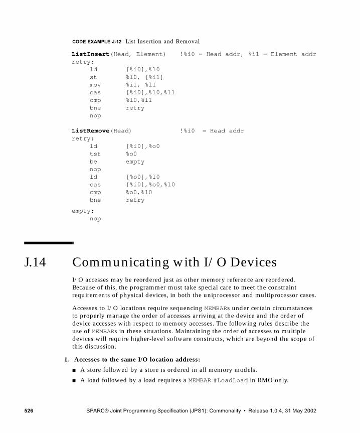
J.14 Communicating with I/O DevicesI/O accesses may be reordered just as other memory reference are reordered. Because of this, the programmer must take special care to meet the constraint requirements of physical devices, in both the uniprocessor and multiprocessor cases.
Accesses to I/O locations require sequencing MEMBARs under certain circumstances to properly manage the order of accesses arriving at the device and the order of device accesses with respect to memory accesses. The following rules describe the use of MEMBARs in these situations. Maintaining the order of accesses to multiple devices will require higher-level software constructs, which are beyond the scope of this discussion.
1. Accesses to the same I/O location address:
■ A store followed by a store is ordered in all memory models.
■ A load followed by a load requires a MEMBAR #LoadLoad in RMO only.
ListInsert(Head, Element) !%i0 = Head addr, %i1 = Element addrretry:
ld [%i0],%l0st %l0, [%i1]mov %i1, %l1cas [%i0],%l0,%l1cmp %l0,%l1bne retrynop
ListRemove(Head) !%i0 = Head addrretry:
ld [%i0],%o0tst %o0be emptynopld [%o0],%l0cas [%i0],%o0,%l0cmp %o0,%l0bne retry
empty:nop
CODE EXAMPLE J-12 List Insertion and Removal
526 SPARC® Joint Programming Specification (JPS1): Commonality • Release 1.0.4, 31 May 2002
Compatibility Note – This MEMBAR is not needed in implementations that provide SPARC V8 compatibility for I/O accesses in RMO.
■ A load followed by a store is ordered in all memory models.
■ A store followed by a load requires MEMBAR #Lookaside between the accesses for all memory models; however, implementations that provide SPARC V8 compatibility for I/O accesses in any of TSO, PSO, and RMO do not need the MEMBAR in any model that provides this compatibility.
2. Accesses to different I/O location addresses:
■ The appropriate ordering MEMBAR is required to guarantee order within a range of addresses assigned to a device.
■ Device-specific synchronization of completion, such as reading back from an address after a store, may be required to coordinate accesses to multiple devices. This is beyond the scope of this discussion.
3. Accesses to an I/O location address and a memory address.
■ A MEMBAR #MemIssue is required between an I/O access and a memory access if it is required that the I/O access reaches global visibility before the memory access reaches global visibility. For example, if the memory location is a lock that controls access to an I/O address, then MEMBAR #MemIssue is required between the last access to the I/O location and the store that clears the lock.
4. Accesses to different I/O location addresses within an implementation-dependent range of addresses are strongly ordered once they reach global visibility. Beyond the point of global visibility there is no guarantee of global order of accesses arriving at different devices having disjoint implementation-dependent address ranges defining the device. Programmers can rely on this behavior from implementations.
5. Accesses to I/O locations protected by a lock in shared memory that is subsequently released, with attention to the above barrier rules, are strongly ordered with respect to any subsequent accesses to those locations that respect the lock.
J.14.1 I/O Registers with Side EffectsI/O registers with side effects are commonly used in hardware devices such as UARTs. One register is used to address an internal register of the I/O device, and a second register is used to transfer data to or from the selected internal register.
In CODE EXAMPLE J-13 and CODE EXAMPLE J-14, let X be the address of a device with two such registers; X.P is a port register, and X.D is a data register. The address of an internal register is stored into X.P; that internal register can then be read or written by loading into or storing from X.D.
Release 1.0.4, 31 May 2002 C. Appendix J • Programming with the Memory Models 527
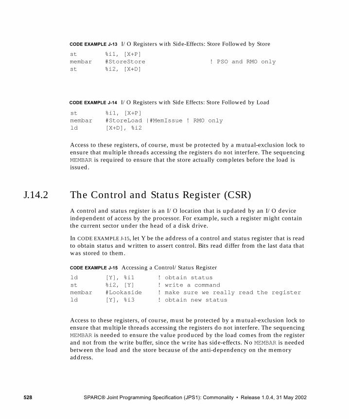
Access to these registers, of course, must be protected by a mutual-exclusion lock to ensure that multiple threads accessing the registers do not interfere. The sequencing MEMBAR is required to ensure that the store actually completes before the load is issued.
J.14.2 The Control and Status Register (CSR)A control and status register is an I/O location that is updated by an I/O device independent of access by the processor. For example, such a register might contain the current sector under the head of a disk drive.
In CODE EXAMPLE J-15, let Y be the address of a control and status register that is read to obtain status and written to assert control. Bits read differ from the last data that was stored to them.
Access to these registers, of course, must be protected by a mutual-exclusion lock to ensure that multiple threads accessing the registers do not interfere. The sequencing MEMBAR is needed to ensure the value produced by the load comes from the register and not from the write buffer, since the write has side-effects. No MEMBAR is needed between the load and the store because of the anti-dependency on the memory address.
st %i1, [X+P]membar #StoreStore ! PSO and RMO onlyst %i2, [X+D]
CODE EXAMPLE J-13 I/O Registers with Side-Effects: Store Followed by Store
st %i1, [X+P]membar #StoreLoad |#MemIssue ! RMO onlyld [X+D], %i2
CODE EXAMPLE J-14 I/O Registers with Side Effects: Store Followed by Load
ld [Y], %i1 ! obtain statusst %i2, [Y] ! write a commandmembar #Lookaside ! make sure we really read the registerld [Y], %i3 ! obtain new status
CODE EXAMPLE J-15 Accessing a Control/Status Register
528 SPARC® Joint Programming Specification (JPS1): Commonality • Release 1.0.4, 31 May 2002
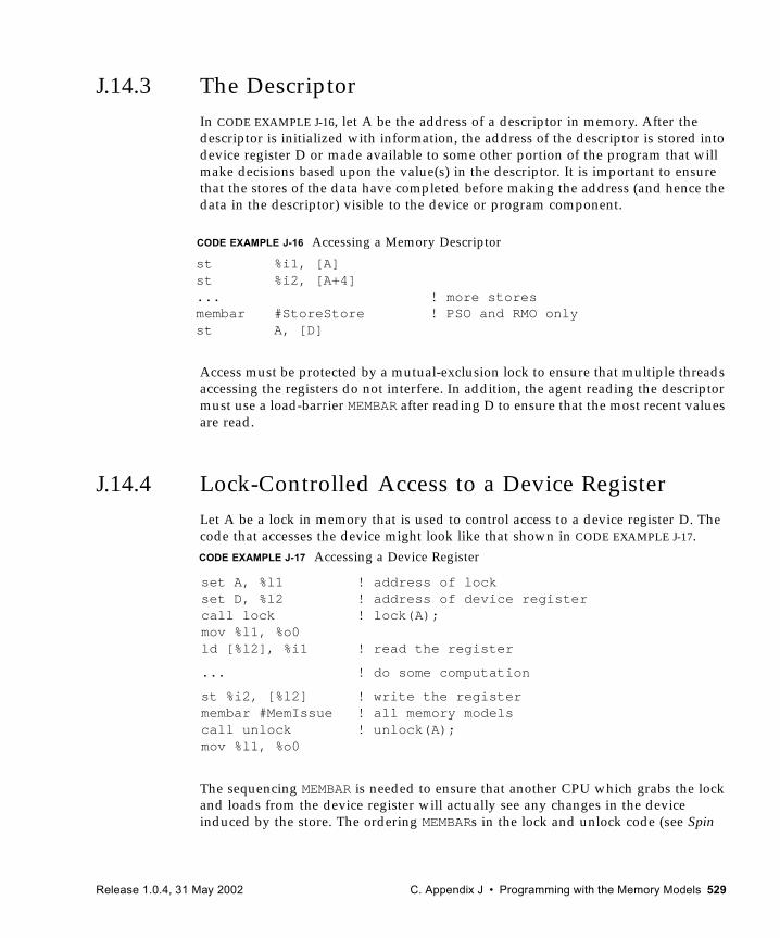
J.14.3 The DescriptorIn CODE EXAMPLE J-16, let A be the address of a descriptor in memory. After the descriptor is initialized with information, the address of the descriptor is stored into device register D or made available to some other portion of the program that will make decisions based upon the value(s) in the descriptor. It is important to ensure that the stores of the data have completed before making the address (and hence the data in the descriptor) visible to the device or program component.
Access must be protected by a mutual-exclusion lock to ensure that multiple threads accessing the registers do not interfere. In addition, the agent reading the descriptor must use a load-barrier MEMBAR after reading D to ensure that the most recent values are read.
J.14.4 Lock-Controlled Access to a Device RegisterLet A be a lock in memory that is used to control access to a device register D. The code that accesses the device might look like that shown in CODE EXAMPLE J-17.
The sequencing MEMBAR is needed to ensure that another CPU which grabs the lock and loads from the device register will actually see any changes in the device induced by the store. The ordering MEMBARs in the lock and unlock code (see Spin
st %i1, [A]st %i2, [A+4]... ! more storesmembar #StoreStore ! PSO and RMO onlyst A, [D]
CODE EXAMPLE J-16 Accessing a Memory Descriptor
set A, %l1 ! address of lockset D, %l2 ! address of device registercall lock ! lock(A);mov %l1, %o0ld [%l2], %i1 ! read the register
... ! do some computation
st %i2, [%l2] ! write the registermembar #MemIssue ! all memory modelscall unlock ! unlock(A);mov %l1, %o0
CODE EXAMPLE J-17 Accessing a Device Register
Release 1.0.4, 31 May 2002 C. Appendix J • Programming with the Memory Models 529
Locks on page 516), while ensuring correctness when protecting ordinary memory, are insufficient for this purpose when accessing device registers. Compare with I/O Registers with Side Effects on page 527.
530 SPARC® Joint Programming Specification (JPS1): Commonality • Release 1.0.4, 31 May 2002
C.APPENDIX K
Changes from SPARC V8 to SPARC V9
This appendix contains only material from The SPARC Architecture Manual, Version 9, The appendix is informative only. It is not part of the SPARC V9 specification.
SPARC V9 is complementary to the SPARC V8 architecture; it does not replace it. SPARC V9 was designed to be a higher-performance peer to SPARC V8.
Application software for the 32-bit SPARC V8 (Version 8) microprocessor architecture can execute, unchanged, on SPARC V9 systems. SPARC V8 software executes natively on SPARC V9-conformant processors; no special compatibility mode is required.
Changes to the SPARC V9 architecture since SPARC V8 are in seven main areas: the trap model, data formats, endianness, the registers, alternate address space access, the instruction set, and the memory model.
K.1 Trap ModelThe trap model, visible only to privileged software, has changed substantially.
■ Instead of one level of traps, four or more levels are now supported. This allows first-level trap handlers, notably register window spill and fill (formerly called overflow and underflow) traps, to execute much faster. Such trap handlers can now execute without costly run-time checks for lower-level trap conditions, such as page faults or a misaligned stack pointer. Also, multiple trap levels support more robust fault-tolerance mechanisms.
■ Most traps no longer change the CWP. Instead, the trap state (including the CWP register) is saved in register stacks called TSTATE, TT, TPC, and TNPC.
■ New instructions (DONE and RETRY) are used instead of RETT to return from a trap handler.
Release 1.0.4, 31 May 2002 C. Appendix K • Changes from SPARC V8 to SPARC V9 531
■ A new instruction (RETURN) is provided for returning from a trap handler running in nonprivileged mode, providing support for user trap handlers.
■ Terminology about privileged-mode execution has changed: from “supervisor/user” to “privileged/nonprivileged.”
■ A new processor state, RED_state, has been added to facilitate processing resets and nested traps that would exceed MAXTL.
K.2 Data FormatsData formats for extended (64-bit) integers have been added.
K.3 Little-Endian SupportData accesses can be either big-endian or little-endian. Bits in the PSTATE register control the implicit endianness of data accesses. Special ASI values are provided to allow specific data accesses to be in a specific endianness.
K.4 Little-Endian Byte OrderIn SPARC V8, all instruction and data accesses were performed in big-endian byte order. SPARC V9 supports both big- and little-endian byte orders for data accesses only; instruction accesses in SPARC V9 are always performed using big-endian order.
K.5 RegistersThese privileged SPARC V8 registers have been deleted:
■ PSR: Processor State Register ■ TBR: Trap Base Register ■ WIM: Window Invalid Mask
532 SPARC® Joint Programming Specification (JPS1): Commonality • Release 1.0.4, 31 May 2002
These registers have been widened from 32 to 64 bits:
■ All integer registers■ All state registers: FSR, PC, nPC, Y
The contents of the following register has changed:
■ FSR: Floating-Point State Register: fcc1, fcc2, and fcc3 (additional floating-point condition code) bits have been added and the register widened to 64 bits.
These SPARC V9 registers are fields within a register in SPARC V8:
■ PIL: Processor Interrupt Level register■ CWP: Current Window Pointer register■ TT[MAXTL]: Trap Type register■ TBA: Trap Base Address register■ VER: Version register ■ CCR: Condition Codes Register
These registers have been added:
■ Sixteen additional double-precision floating-point registers, f[32]–f [62], which are aliased with and overlap eight additional quad-precision floating-point registers, f [32]–f[60]
■ FPRS: Floating-Point Register State register
■ ASI: ASI register
■ PSTATE: Processor State register
■ TL: Trap Level register
■ TPC[MAXTL]: Trap Program Counter register
■ TNPC[MAXTL]: Trap Next Program Counter register
■ TSTATE[MAXTL]: Trap State register
■ TICK: Hardware clock-tick counter
■ CANSAVE: Savable windows register
■ CANRESTORE: Restorable windows register
■ OTHERWIN: Other Windows register
■ CLEANWIN: Clean Windows register
■ WSTATE: Window State register
The SPARC V9 CWP register is incremented during a SAVE instruction and decremented during a RESTORE instruction. Although this is the opposite of PSR.CWP’s behavior in SPARC V8, the only software it should affect is a few trap handlers that operate in privileged mode, and those must be rewritten for SPARC V9 anyway. This change will have no effect on nonprivileged software.
Release 1.0.4, 31 May 2002 C. Appendix K • Changes from SPARC V8 to SPARC V9 533
K.6 Alternate Space AccessIn SPARC V8, access to all alternate address spaces is privileged. In SPARC V9, loads and stores to ASIs 0016–7F16 are privileged; those to ASIs 8016–FF16 are nonprivileged. That is, load- and store-alternate instructions to one-half of the alternate spaces can now be used in user code.
K.7 Instruction SetAll changes to the instruction set were made such that application software written for SPARC V8 can run unchanged on a SPARC V9 processor. Application software written for SPARC V8 should not even be able to detect that its instructions now process 64-bit values.
The definitions of the following instructions were extended or modified to work with the 64-bit model:
■ FCMP, FCMPE: Floating-Point Compare: Can set any of the four floating-point condition codes
■ LDUW, LDUWA (same as “LD, LDA” in SPARC V8)
■ LDFSR, STFSR: Load/Store FSR: Only affect low-order 32 bits of FSR
■ RDASR/WRASR: Read/Write State Registers: Access additional registers
■ SAVE/RESTORE
■ SETHI
■ SRA, SRL, SLL: Shifts: Split into 32-bit and 64-bit versions
■ Tcc: (was Ticc): Operates with either the 32-bit integer condition codes (icc), or the 64-bit integer condition codes (xcc)
■ All other arithmetic operations now operate on 64-bit operands and produce 64-bit results. Application software written for SPARC V8 cannot detect that arithmetic operations are now 64 bits wide. This is due to retention of the 32-bit integer condition codes (icc), addition of 64-bit integer condition codes (xcc), and the carry-propagation rules of two’s-complement arithmetic.
The following instructions have been added to provide support for 64-bit operations and/or addressing:
■ F[sdq]TOx: Convert floating point to 64-bit word
■ FxTO[sdq]: Convert 64-bit word to floating point
■ FMOV[dq]: Floating-point Move, double and quad
■ FNEG[dq]: Floating-point Negate, double and quad
534 SPARC® Joint Programming Specification (JPS1): Commonality • Release 1.0.4, 31 May 2002
■ FABS[dq]: Floating-point Absolute Value, double and quad
■ LDDFA, STDFA, LDFA, STFA: Alternate address space forms of LDDF, STDF, LDF, and STF
■ LDSW: Load a signed word
■ LDSWA: Load a signed word from an alternate space
■ LDX: Load an extended word
■ LDXA: Load an extended word from an alternate space
■ LDXFSR: Load all 64 bits of the FSR register
■ STX: Store an extended word
■ STXA: Store an extended word into an alternate space
■ STXFSR: Store all 64 bits of the FSR register
The following instructions have been added to support the new trap model:
■ DONE: Return from trap and skip instruction that trapped
■ RDPR and WRPR: Read and Write privileged registers
■ RESTORED: Adjust state of register windows after RESTORE
■ RETRY: Return from trap and reexecute instruction that trapped
■ RETURN: Return
■ SAVED: Adjust state of register windows after SAVE
■ SIR: Signal Monitor (generate software-initiated reset)
The following instructions have been added to support implementation of higher-performance systems:
■ BPcc: Branch on integer condition code with prediction
■ BPr: Branch on integer register contents with prediction
■ CASA, CASXA: Compare and Swap from an alternate space
■ FBPfcc: Branch on floating-point condition code with prediction
■ FLUSHW: Flush windows
■ FMOVcc: Move floating-point register if condition code is satisfied
■ FMOVr: Move floating-point register if integer register contents satisfy condition
■ LDQF(A), STQF(A): Load/Store Quad Floating-point (in an alternate space)
■ MOVcc: Move integer register if condition code is satisfied
■ MOVr: Move integer register if register contents satisfy condition
■ MULX: Generic 64-bit multiply
■ POPC: Population Count
■ PREFETCH, PREFETCHA: Prefetch Data
■ SDIVX, UDIVX: Signed and Unsigned 64-bit divide
Release 1.0.4, 31 May 2002 C. Appendix K • Changes from SPARC V8 to SPARC V9 535
The definitions of the following instructions have changed:
■ IMPDEPn: SPARC V8 CPop instructions have been replaced by VIS, IMPDEP2A, and IMPDEP2B instructions.
The following instruction was added to support memory synchronization:
■ MEMBAR: Memory barrier
The following instructions have been deleted:
■ Coprocessor loads and stores
■ RDTBR and WRTBR: TBR no longer exists. It has been replaced by TBA, which can be read/written with RDPR/WRPR instructions.
■ RDWIM and WRWIM: WIM no longer exists. WIM has been subsumed by several register-window state registers.
■ RDPSR and WRPSR: PSR no longer exists. It has been replaced by several separate registers which are read/written with other instructions.
■ RETT: Return from trap (replaced by DONE/RETRY).
■ STDFQ: Store Double from Floating-point Queue (replaced by the RDPR FQ instruction).
K.8 Memory ModelSPARC V9 defines a new memory model called Relaxed Memory Order (RMO). This very weak model allows the CPU hardware to schedule memory accesses such as loads and stores in nearly any order, as long as the program computes the correct answer. Hence, the hardware can instantaneously adjust to resource contentions and schedule accesses in the most efficient order, leading to much faster memory operations and better performance.
536 SPARC® Joint Programming Specification (JPS1): Commonality • Release 1.0.4, 31 May 2002
C.APPENDIX L
Address Space Identifiers
This appendix describes address space identifiers (ASIs) in the following sections:
■ Address Space Identifiers and Address Spaces on page 537■ ASI Values on page 538■ ASI Assignments on page 538
L.1 Address Space Identifiers and Address SpacesA SPARC V9 processor provides an address space identifier (ASI) with every address sent to memory. The ASI does the following:
■ Distinguishes between different address spaces■ Provides an attribute that is unique to an address space■ Maps internal control and diagnostics registers within a processor
The memory management hardware uses a 64-bit virtual address and an 8-bit ASI to generate a physical address. This physical address space can be accessed through virtual-to-physical address mapping or through the MMU bypass mode.
SPARC V9 also extended the limit of virtual addresses from 32 bits to 64 bits for each address space. SPARC V9 supports 32-bit addressing through masking of the upper 32 bits to 0 when the address mask (AM) bit in the PSTATE register is set.
Release 1.0.4, 31 May 2002 C. Appendix L • Address Space Identifiers 537
L.2 ASI ValuesThe SPARC V9 address space identifier (ASI) is evenly divided into restricted and unrestricted halves. ASIs in the range 0016–7F16 are restricted. ASIs in the range 8016–FF16 are unrestricted. An attempt by nonprivileged software to access a restricted ASI causes a privileged_action trap.
ASIs in the ranges 0416–1116, 1816–1916, 2416–2C16, 7016–7116, 7816–7916, and 8016–FF16 are called normal or translating ASIs. These ASIs are translated by the MMU.
Bypass ASIs are in the range 1416–1516 and 1C16–1D16. These ASIs are not translated by the MMU. Instead, they pass through their virtual addresses as physical addresses.
Implementation-dependent ASIs may or may not be translated by the MMU. See Appendix L in the Implementation Supplement for a given implementation for detailed information about specific implementation-dependent ASIs.
L.3 ASI AssignmentsEvery load or store address in a SPARC V9 processor has an 8-bit Address Space Identifier (ASI) appended to the virtual address (VA). The VA plus the ASI fully specify the address. For instruction fetches and for data loads or stores that do not use the load or store alternate instructions, the ASI is an implicit ASI generated by the hardware. If a load alternate or store alternate instruction is used, the value of the ASI can be specified in the %asi register or as an immediate value in the instruction. In practice, ASIs are not only used to differentiate address spaces but are also used for other functions like referencing registers in the MMU unit.
L.3.1 Supported ASIs TABLE L-1 lists both the SPARC V9 architecture-defined ASIs and ASIs that were not defined in SPARC V9 but are required for JPS1 processors.
ASIs marked with a closed bullet (● ) are SPARC V9 architecture-defined ASIs. All operand sizes are supported when accessing one of these ASIs.
ASIs marked with an open bullet (❍ ) were not defined in SPARC V9 but are required to be implemented in all JPS1 processors. These ASIs can be used only with LDXA, STXA, LDDFA, or STDFA instructions, unless otherwise noted. An attempt to access
538 SPARC® Joint Programming Specification (JPS1): Commonality • Release 1.0.4, 31 May 2002
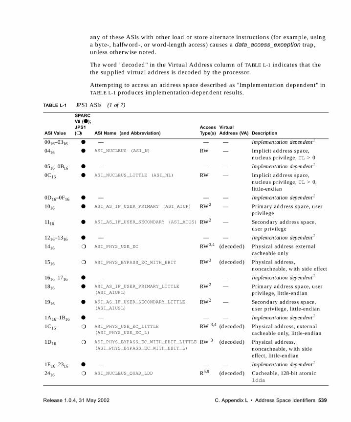
any of these ASIs with other load or store alternate instructions (for example, using a byte-, halfword-, or word-length access) causes a data_access_exception trap, unless otherwise noted.
The word "decoded" in the Virtual Address column of TABLE L-1 indicates that the the supplied virtual address is decoded by the processor.
Attempting to access an address space described as "Implementation dependent" in TABLE L-1 produces implementation-dependent results.
TABLE L-1 JPS1 ASIs (1 of 7)
ASI Value
SPARC V9 (● );JPS1 (❍ ) ASI Name (and Abbreviation)
AccessType(s)
Virtual Address (VA) Description
0016–0316 ● — — — Implementation dependent1
0416 ● ASI_NUCLEUS (ASI_N) RW — Implicit address space, nucleus privilege, TL > 0
0516–0B16 ● — — — Implementation dependent1
0C16 ● ASI_NUCLEUS_LITTLE (ASI_NL) RW — Implicit address space, nucleus privilege, TL > 0, little-endian
0D16–0F16 ● — — — Implementation dependent1
1016 ● ASI_AS_IF_USER_PRIMARY (ASI_AIUP) RW2 — Primary address space, user privilege
1116 ● ASI_AS_IF_USER_SECONDARY (ASI_AIUS) RW2 — Secondary address space, user privilege
1216–1316 ● — — — Implementation dependent1
1416 ❍ ASI_PHYS_USE_EC RW3,4 (decoded) Physical address external cacheable only
1516 ❍ ASI_PHYS_BYPASS_EC_WITH_EBIT RW3 (decoded) Physical address, noncacheable, with side effect
1616–1716 ● — — — Implementation dependent1
1816 ● ASI_AS_IF_USER_PRIMARY_LITTLE (ASI_AIUPL)
RW2 — Primary address space, user privilege, little-endian
1916 ● ASI_AS_IF_USER_SECONDARY_LITTLE (ASI_AIUSL)
RW2 — Secondary address space, user privilege, little-endian
1A16–1B16 ● — — — Implementation dependent1
1C16 ❍ ASI_PHYS_USE_EC_LITTLE (ASI_PHYS_USE_EC_L)
RW 3,4 (decoded) Physical address, external cacheable only, little-endian
1D16 ❍ ASI_PHYS_BYPASS_EC_WITH_EBIT_LITTLE(ASI_PHYS_BYPASS_EC_WITH_EBIT_L)
RW 3 (decoded) Physical address, noncacheable, with side effect, little-endian
1E16–2316 ● — — — Implementation dependent1
2416 ❍ ASI_NUCLEUS_QUAD_LDD R5,9 (decoded) Cacheable, 128-bit atomic ldda
Release 1.0.4, 31 May 2002 C. Appendix L • Address Space Identifiers 539
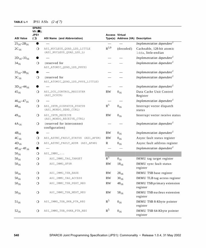
2516–2B16 ● — — — Implementation dependent1
2C16 ❍ ASI_NUCLEUS_QUAD_LDD_LITTLE (ASI_NUCLEUS_QUAD_LDD_L)
R5,9 (decoded) Cacheable, 128-bit atomic ldda, little-endian
2D16–3316 ● — — — Implementation dependent1
3416 ❍ (reserved for ASI_ATOMIC_QUAD_LDD_PHYS)
— — Implementation dependent1
3516–3B16 ● — — — Implementation dependent1
3C16 ❍ (reserved for ASI_ATOMIC_QUAD_LDD_PHYS_LITTLE)
— — Implementation dependent1
3D16–4416 ● — — — Implementation dependent1
4516 ❍ ASI_DCU_CONTROL_REGISTER (ASI_DCUCR)
RW 016 Data Cache Unit Control Register
4616–4716 ❍ — — — Implementation dependent1
4816 ❍ ASI_INTR_DISPATCH_STATUS (ASI_MONDO_SEND_CTRL)
R5 016 Interrupt vector dispatch status
4916 ❍ ASI_INTR_RECEIVE (ASI_MONDO_RECEIVE_CTRL)
RW 016 Interrupt vector receive status
4A16 ❍ (reserved for interconnect configuration)
— — Implementation dependent1
4B16 ● — RW 016 Implementation dependent1
4C16 ❍ ASI_ASYNC_FAULT_STATUS (ASI_AFSR) RW 016 Async fault status register
4D16 ❍ ASI_ASYNC_FAULT_ADDR (ASI_AFAR) R 016 Async fault address register
4E16–4F16 ● — — — Implementation dependent1
5016 ❍ ASI_IMMU_...
5016 ❍ ASI_IMMU_TAG_TARGET R5 016 IMMU tag target register
5016 ❍ ASI_IMMU_SFSR RW 1816 IMMU sync fault status register
5016 ❍ ASI_IMMU_TSB_BASE RW 2816 IMMU TSB base register
5016 ❍ ASI_IMMU_TAG_ACCESS RW 3016 IMMU TLB tag access register
5016 ❍ ASI_IMMU_TSB_PEXT_REG RW 4816 IMMU TSB primary extension register
5016 ❍ ASI_IMMU_TSB_NEXT_REG RW 5816 IMMU TSB nucleus extension register
5116 ❍ ASI_IMMU_TSB_8KB_PTR_REG R5 016 IMMU TSB 8-Kbyte pointer register
5216 ❍ ASI_IMMU_TSB_64KB_PTR_REG R5 016 IMMU TSB 64-Kbyte pointer register
TABLE L-1 JPS1 ASIs (2 of 7)
ASI Value
SPARC V9 (● );JPS1 (❍ ) ASI Name (and Abbreviation)
AccessType(s)
Virtual Address (VA) Description
540 SPARC® Joint Programming Specification (JPS1): Commonality • Release 1.0.4, 31 May 2002
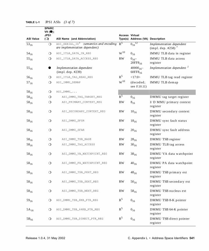
5316 ❍ ASI_SERIAL_ID‡ (semantics and encoding are implementation dependent)
R5 01612 Implementation dependent
(impl. dep. #258) 7
5416 ❍ ASI_ITLB_DATA_IN_REG W10 016 IMMU TLB data in register
5516 ❍ ASI_ITLB_DATA_ACCESS_REG RW 016–20FF816
IMMU TLB data access register
5516 ● Implementation dependent(impl. dep. #239)
4000016–60FF816
Implementation dependent 1
5616 ❍ ASI_ITLB_TAG_READ_REG R5 <17:0> IMMU TLB tag read register
5716 ❍ ASI_IMMU_DEMAP W10 (decoded; see F.10.11)
IMMU TLB demap
5816 ❍ ASI_DMMU_...
5816 ❍ ASI_DMMU_TAG_TARGET_REG R5 016 DMMU tag target register
5816 ❍ ASI_PRIMARY_CONTEXT_REG RW 816 I/D MMU primary context register
5816 ❍ ASI_SECONDARY_CONTEXT_REG RW 1016 DMMU secondary context register
5816 ❍ ASI_DMMU_SFSR RW 1816 DMMU sync fault status register
5816 ❍ ASI_DMMU_SFAR RW 2016 DMMU sync fault address register
5816 ❍ ASI_DMMU_TSB_BASE RW 2816 DMMU TSB register
5816 ❍ ASI_DMMU_TAG_ACCESS RW 3016 DMMU TLB tag access register
5816 ❍ ASI_DMMU_VA_WATCHPOINT_REG RW 3816 DMMU VA data watchpoint register
5816 ❍ ASI_DMMU_PA_WATCHPOINT_REG RW 4016 DMMU PA data watchpoint register
5816 ❍ ASI_DMMU_TSB_PEXT_REG RW 4816 DMMU TSB primary ext register
5816 ❍ ASI_DMMU_TSB_SEXT_REG RW 5016 DMMU TSB secondary ext register
5816 ❍ ASI_DMMU_TSB_NEXT_REG RW 5816 DMMU TSB nucleus ext register
5916 ❍ ASI_DMMU_TSB_8KB_PTR_REG R5 016 DMMU TSB 8-K pointer register
5A16 ❍ ASI_DMMU_TSB_64KB_PTR_REG R5 016 DMMU TSB 64-K pointer register
5B16 ❍ ASI_DMMU_TSB_DIRECT_PTR_REG R5 016 DMMU TSB direct pointer register
TABLE L-1 JPS1 ASIs (3 of 7)
ASI Value
SPARC V9 (● );JPS1 (❍ ) ASI Name (and Abbreviation)
AccessType(s)
Virtual Address (VA) Description
Release 1.0.4, 31 May 2002 C. Appendix L • Address Space Identifiers 541
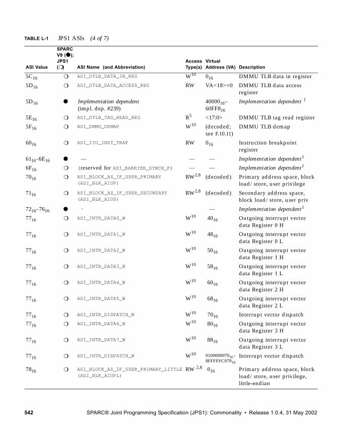
5C16 ❍ ASI_DTLB_DATA_IN_REG W10 016 DMMU TLB data in register
5D16 ❍ ASI_DTLB_DATA_ACCESS_REG RW VA<18>=0 DMMU TLB data access register
5D16 ● Implementation dependent(impl. dep. #239)
4000016–60FF816
Implementation dependent 1
5E16 ❍ ASI_DTLB_TAG_READ_REG R5 <17:0> DMMU TLB tag read register
5F16 ❍ ASI_DMMU_DEMAP W10 (decoded; see F.10.11)
DMMU TLB demap
6016 ❍ ASI_IIU_INST_TRAP RW 016 Instruction breakpoint register
6116–6E16 ● — — — Implementation dependent1
6F16 ❍ (reserved for ASI_BARRIER_SYNCH_P) — — Implementation dependent1
7016 ❍ ASI_BLOCK_AS_IF_USER_PRIMARY(ASI_BLK_AIUP)
RW2,8 (decoded) Primary address space, block load/store, user privilege
7116 ❍ ASI_BLOCK_AS_IF_USER_SECONDARY(ASI_BLK_AIUS)
RW2,8 (decoded) Secondary address space, block load/store, user priv
7216–7616 ● — — Implementation dependent1
7716 ❍ ASI_INTR_DATA0_W W10 4016 Outgoing interrupt vector data Register 0 H
7716 ❍ ASI_INTR_DATA1_W W10 4816 Outgoing interrupt vector data Register 0 L
7716 ❍ ASI_INTR_DATA2_W W10 5016 Outgoing interrupt vector data Register 1 H
7716 ❍ ASI_INTR_DATA3_W W10 5816 Outgoing interrupt vector data Register 1 L
7716 ❍ ASI_INTR_DATA4_W W10 6016 Outgoing interrupt vector data Register 2 H
7716 ❍ ASI_INTR_DATA5_W W10 6816 Outgoing interrupt vector data Register 2 L
7716 ❍ ASI_INTR_DISPATCH_W W10 7016 Interrupt vector dispatch
7716 ❍ ASI_INTR_DATA6_W W10 8016 Outgoing interrupt vector data Register 3 H
7716 ❍ ASI_INTR_DATA7_W W10 8816 Outgoing interrupt vector data Register 3 L
7716 ❍ ASI_INTR_DISPATCH_W W10 010000007016–8FFFFFC07016
Interrupt vector dispatch
7816 ❍ ASI_BLOCK_AS_IF_USER_PRIMARY_LITTLE(ASI_BLK_AIUPL)
RW 2,8 016 Primary address space, block load/store, user privilege, little-endian
TABLE L-1 JPS1 ASIs (4 of 7)
ASI Value
SPARC V9 (● );JPS1 (❍ ) ASI Name (and Abbreviation)
AccessType(s)
Virtual Address (VA) Description
542 SPARC® Joint Programming Specification (JPS1): Commonality • Release 1.0.4, 31 May 2002
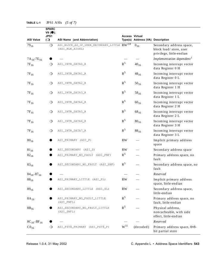
7916 ❍ ASI_BLOCK_AS_IF_USER_SECONDARY_LITTLE
(ASI_BLK_AIUSL)RW2,8 016 Secondary address space,
block load/store, user privilege, little-endian
7A16-7E16 ● — — — Implementation dependent1
7F16 ❍ ASI_INTR_DATA0_R R5 4016 Incoming interrupt vector data Register 0 H
7F16 ❍ ASI_INTR_DATA1_R R5 4816 Incoming interrupt vector data Register 0 L
7F16 ❍ ASI_INTR_DATA2_R R5 5016 Incoming interrupt vector data Register 1 H
7F16 ❍ ASI_INTR_DATA3_R R5 5816 Incoming interrupt vector data Register 1 L
7F16 ❍ ASI_INTR_DATA4_R R5 6016 Incoming interrupt vector data Register 2 H
7F16 ❍ ASI_INTR_DATA5_R R5 6816 Incoming interrupt vector data Register 2 L
7F16 ❍ ASI_INTR_DATA6_R R5 8016 Incoming interrupt vector data Register 3 H
7F16 ❍ ASI_INTR_DATA7_R R5 8816 Incoming interrupt vector data Register 3 L
8016 ● ASI_PRIMARY (ASI_P) RW — Implicit primary address space
8116 ● ASI_SECONDARY (ASI_S) RW — Secondary address space
8216 ● ASI_PRIMARY_NO_FAULT (ASI_PNF) R5 — Primary address space, no fault
8316 ● ASI_SECONDARY_NO_FAULT (ASI_SNF) R5 — Secondary address space, no fault
8416–8716 ● — — — Reserved
8816 ● ASI_PRIMARY_LITTLE (ASI_PL) RW — Implicit primary address space, little-endian
8916 ● ASI_SECONDARY_LITTLE (ASI_SL) RW — Secondary address space, little-endian
8A16 ● ASI_PRIMARY_NO_FAULT_LITTLE (ASI_PNFL)
R5 — Primary address space, no fault, little-endian
8B16 ● ASI_SECONDARY_NO_FAULT_LITTLE (ASI_SNFL)
R5 — Physical address, noncacheable, with side effect, little-endian
8C16–BF16 ● — — — Reserved
C016 ❍ ASI_PST8_PRIMARY (ASI_PST8_P) W11 (decoded) Primary address space, 8×8-bit partial store
TABLE L-1 JPS1 ASIs (5 of 7)
ASI Value
SPARC V9 (● );JPS1 (❍ ) ASI Name (and Abbreviation)
AccessType(s)
Virtual Address (VA) Description
Release 1.0.4, 31 May 2002 C. Appendix L • Address Space Identifiers 543
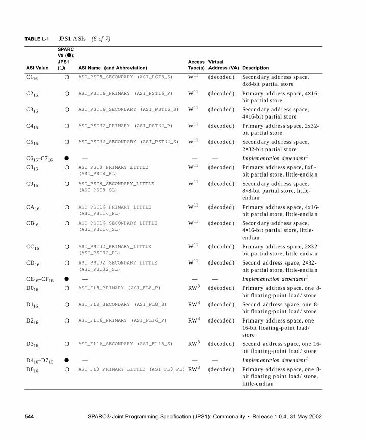
C116 ❍ ASI_PST8_SECONDARY (ASI_PST8_S) W11 (decoded) Secondary address space, 8x8-bit partial store
C216 ❍ ASI_PST16_PRIMARY (ASI_PST16_P) W11 (decoded) Primary address space, 4×16-bit partial store
C316 ❍ ASI_PST16_SECONDARY (ASI_PST16_S) W11 (decoded) Secondary address space, 4×16-bit partial store
C416 ❍ ASI_PST32_PRIMARY (ASI_PST32_P) W11 (decoded) Primary address space, 2x32-bit partial store
C516 ❍ ASI_PST32_SECONDARY (ASI_PST32_S) W11 (decoded) Secondary address space, 2×32-bit partial store
C616–C716 ● — — — Implementation dependent1
C816 ❍ ASI_PST8_PRIMARY_LITTLE (ASI_PST8_PL)
W11 (decoded) Primary address space, 8x8-bit partial store, little-endian
C916 ❍ ASI_PST8_SECONDARY_LITTLE (ASI_PST8_SL)
W11 (decoded) Secondary address space, 8×8-bit partial store, little-endian
CA16 ❍ ASI_PST16_PRIMARY_LITTLE (ASI_PST16_PL)
W11 (decoded) Primary address space, 4x16-bit partial store, little-endian
CB16 ❍ ASI_PST16_SECONDARY_LITTLE (ASI_PST16_SL)
W11 (decoded) Secondary address space, 4×16-bit partial store, little-endian
CC16 ❍ ASI_PST32_PRIMARY_LITTLE (ASI_PST32_PL)
W11 (decoded) Primary address space, 2×32-bit partial store, little-endian
CD16 ❍ ASI_PST32_SECONDARY_LITTLE (ASI_PST32_SL)
W11 (decoded) Second address space, 2×32-bit partial store, little-endian
CE16–CF16 ● — — — Implementation dependent1
D016 ❍ ASI_FL8_PRIMARY (ASI_FL8_P) RW8 (decoded) Primary address space, one 8-bit floating-point load/store
D116 ❍ ASI_FL8_SECONDARY (ASI_FL8_S) RW8 (decoded) Second address space, one 8-bit floating-point load/store
D216 ❍ ASI_FL16_PRIMARY (ASI_FL16_P) RW8 (decoded) Primary address space, one 16-bit floating-point load/store
D316 ❍ ASI_FL16_SECONDARY (ASI_FL16_S) RW8 (decoded) Second address space, one 16-bit floating-point load/store
D416–D716 ● — — — Implementation dependent1
D816 ❍ ASI_FL8_PRIMARY_LITTLE (ASI_FL8_PL) RW8 (decoded) Primary address space, one 8-bit floating point load/store, little-endian
TABLE L-1 JPS1 ASIs (6 of 7)
ASI Value
SPARC V9 (● );JPS1 (❍ ) ASI Name (and Abbreviation)
AccessType(s)
Virtual Address (VA) Description
544 SPARC® Joint Programming Specification (JPS1): Commonality • Release 1.0.4, 31 May 2002
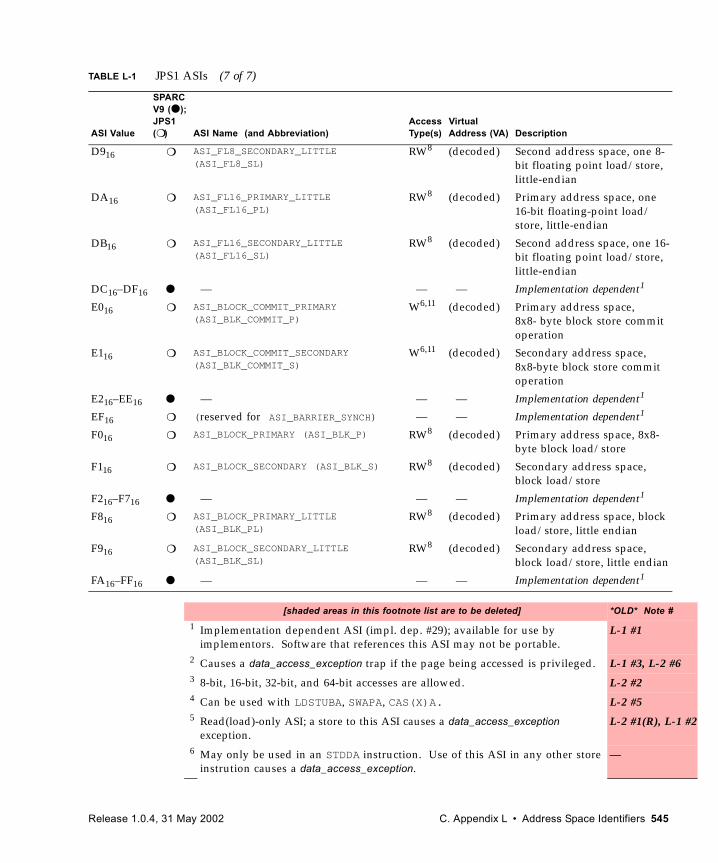
#2
D916 ❍ ASI_FL8_SECONDARY_LITTLE (ASI_FL8_SL)
RW8 (decoded) Second address space, one 8-bit floating point load/store, little-endian
DA16 ❍ ASI_FL16_PRIMARY_LITTLE (ASI_FL16_PL)
RW8 (decoded) Primary address space, one 16-bit floating-point load/store, little-endian
DB16 ❍ ASI_FL16_SECONDARY_LITTLE (ASI_FL16_SL)
RW8 (decoded) Second address space, one 16-bit floating point load/store, little-endian
DC16–DF16 ● — — — Implementation dependent1
E016 ❍ ASI_BLOCK_COMMIT_PRIMARY (ASI_BLK_COMMIT_P)
W6,11 (decoded) Primary address space, 8x8- byte block store commit operation
E116 ❍ ASI_BLOCK_COMMIT_SECONDARY (ASI_BLK_COMMIT_S)
W6,11 (decoded) Secondary address space, 8x8-byte block store commit operation
E216–EE16 ● — — — Implementation dependent1
EF16 ❍ (reserved for ASI_BARRIER_SYNCH) — — Implementation dependent1
F016 ❍ ASI_BLOCK_PRIMARY (ASI_BLK_P) RW8 (decoded) Primary address space, 8x8- byte block load/store
F116 ❍ ASI_BLOCK_SECONDARY (ASI_BLK_S) RW8 (decoded) Secondary address space, block load/store
F216–F716 ● — — — Implementation dependent1
F816 ❍ ASI_BLOCK_PRIMARY_LITTLE (ASI_BLK_PL)
RW8 (decoded) Primary address space, block load/store, little endian
F916 ❍ ASI_BLOCK_SECONDARY_LITTLE (ASI_BLK_SL)
RW8 (decoded) Secondary address space, block load/store, little endian
FA16–FF16 ● — — — Implementation dependent1
[shaded areas in this footnote list are to be deleted] *OLD* Note #
1 Implementation dependent ASI (impl. dep. #29); available for use by implementors. Software that references this ASI may not be portable.
L-1 #1
2 Causes a data_access_exception trap if the page being accessed is privileged. L-1 #3, L-2 #6 3 8-bit, 16-bit, 32-bit, and 64-bit accesses are allowed. L-2 #2 4 Can be used with LDSTUBA, SWAPA, CAS(X)A. L-2 #5 5 Read(load)-only ASI; a store to this ASI causes a data_access_exception
exception.L-2 #1(R), L-1
6 May only be used in an STDDA instruction. Use of this ASI in any other store instrution causes a data_access_exception.
—
TABLE L-1 JPS1 ASIs (7 of 7)
ASI Value
SPARC V9 (● );JPS1 (❍ ) ASI Name (and Abbreviation)
AccessType(s)
Virtual Address (VA) Description
Release 1.0.4, 31 May 2002 C. Appendix L • Address Space Identifiers 545
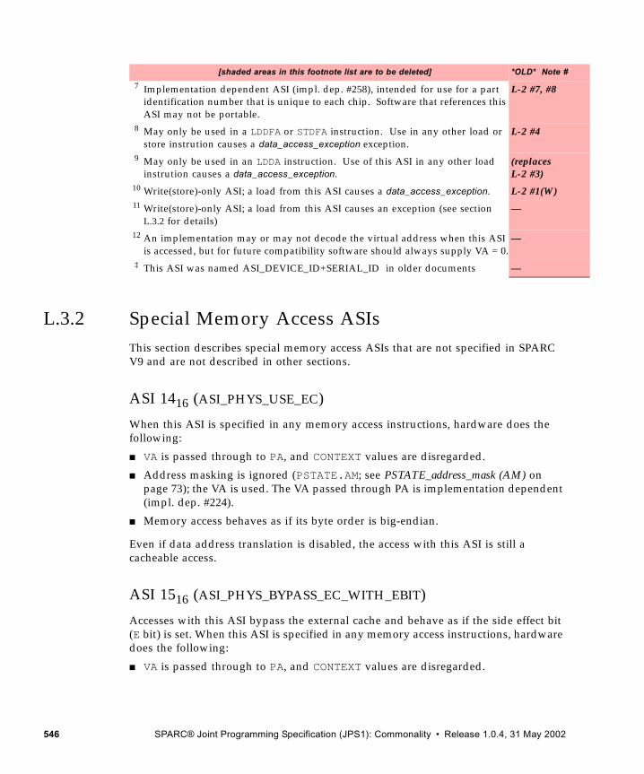
L.3.2 Special Memory Access ASIsThis section describes special memory access ASIs that are not specified in SPARC V9 and are not described in other sections.
ASI 1416 (ASI_PHYS_USE_EC)
When this ASI is specified in any memory access instructions, hardware does the following:
■ VA is passed through to PA, and CONTEXT values are disregarded.
■ Address masking is ignored (PSTATE.AM; see PSTATE_address_mask (AM) on page 73); the VA is used. The VA passed through PA is implementation dependent (impl. dep. #224).
■ Memory access behaves as if its byte order is big-endian.
Even if data address translation is disabled, the access with this ASI is still a cacheable access.
ASI 1516 (ASI_PHYS_BYPASS_EC_WITH_EBIT)
Accesses with this ASI bypass the external cache and behave as if the side effect bit (E bit) is set. When this ASI is specified in any memory access instructions, hardware does the following:
■ VA is passed through to PA, and CONTEXT values are disregarded.
7 Implementation dependent ASI (impl. dep. #258), intended for use for a part identification number that is unique to each chip. Software that references this ASI may not be portable.
L-2 #7, #8
8 May only be used in a LDDFA or STDFA instruction. Use in any other load or store instrution causes a data_access_exception exception.
L-2 #4
9 May only be used in an LDDA instruction. Use of this ASI in any other load instrution causes a data_access_exception.
(replacesL-2 #3)
10 Write(store)-only ASI; a load from this ASI causes a data_access_exception. L-2 #1(W) 11 Write(store)-only ASI; a load from this ASI causes an exception (see section
L.3.2 for details)—
12 An implementation may or may not decode the virtual address when this ASI is accessed, but for future compatibility software should always supply VA = 0.
—
‡ This ASI was named ASI_DEVICE_ID+SERIAL_ID in older documents —
[shaded areas in this footnote list are to be deleted] *OLD* Note #
546 SPARC® Joint Programming Specification (JPS1): Commonality • Release 1.0.4, 31 May 2002
■ Address masking is ignored (PSTATE.AM; see PSTATE_address_mask (AM) on page 73); the VA is used. The VA passed through PA is implementation dependent (impl. dep. #224).
■ Memory access behaves as if its byte order is big-endian.
ASI 1C16 (ASI_PHYS_USE_EC_LITTLE)
Accesses with this ASI are cacheable. This ASI is a little-endian version of ASI 1416. When this ASI is specified in any memory access instructions, hardware does the following:
■ VA is passed through to PA, and CONTEXT values are disregarded.
■ Address masking is ignored (PSTATE.AM; see PSTATE_address_mask (AM) on page 73); the VA is used. The VA passed through PA is implementation dependent (impl. dep. #224).
■ Memory access behaves as if its byte order is little-endian.
ASI 1D16 (ASI_PHYS_BYPASS_EC_WITH_EBIT_LITTLE)
Accesses with this ASI bypass the external cache and behave as if the side effect bit (E bit) is set. This ASI is a little-endian version of ASI 1516. When this ASI is specified in any memory access instructions, hardware does the following:
■ VA is passed through to PA, and CONTEXT values are disregarded.
■ Address masking is ignored (PSTATE.AM; see PSTATE_address_mask (AM) on page 73); the VA is used. The VA passed through PA is implementation dependent (impl. dep. #224).
■ Memory access behaves as if its byte order is little-endian.
ASIs 2416 and 2C16 (Load Quadword ASIs)
ASIs 2416 (ASI_NUCLEUS_QUAD_LDD) and 2C16 (ASI_NUCLEUS_QUAD_LDD_LITTLE) exist for use with the LDDA instruction as Load Quadword operations (see A.30 on page 251).
When these ASIs are used with LDDA for Load Quadword, a mem_address_not_aligned exception is generated if the operand address is not 16-byte aligned.
If these ASIs are used with any other Load Alternate instruction or any Store Alternate instruction, a data_access_exception is always generated and mem_address_not_aligned is not generated.
Release 1.0.4, 31 May 2002 C. Appendix L • Address Space Identifiers 547
ASI 6016 (ASI_IIU_INST_TRAP)
See Instruction Trap Register on page 96 for a description of ASI 6016 and its uses.
Block Load and Store ASIs
ASIs 7016, 7116, 7816, 7916, E016, E116, F016, F116, F816, and F916 exist for use with LDDFA and STDFA instructions as Block Load and Block Store operations (see A.4 on page 199).
When these ASIs are used with LDDFA (STDFA) for Block Load (Store), a mem_address_not_aligned exception is generated if the operand address is not 64-byte aligned.
ASIs E016 and E116 are only defined for use in Block Store with Commit operations (using the STDFA opcode). Neither ASI E016 nor E116 should be used with LDDFA; however, if it is, the following behavior occurs:
1. IMPL. DEP. #255: For LDDFA with ASI E016 or E116, if a destination register number rd is specified which is not a multiple of 8 ("misaligned" rd), it is implementation dependent whether the processor generates a data_access_exception or illegal_instruction exception.
2. IMPL. DEP. #256: For LDDFA with ASI E016 or E116, if a memory address is specified with less than 64-byte alignment, it is implementation dependent whether the processor generates a data_access_exception, mem_address_not_aligned, or LDDF_mem_address_not_aligned exception.
3. If both rd and the memory address are correctly aligned, a data_access_exception occurs.
If a Block Load or Block Store ASI is used with any other Load Alternate or Store Alternate instruction, a data_access_exception exception is always generated and mem_address_not_aligned is not generated.
Partial Store ASIs
ASIs C016–C516 and C816–CD16 exist for use with the STDFA instruction as Partial Store operations (see A.42 on page 282).
When these ASIs are used with STDFA for Partial Store, a mem_address_not_aligned exception is generated if the operand address is not 8-byte aligned and an illegal_instruction exception is generated if i = 1 in the instruction.
548 SPARC® Joint Programming Specification (JPS1): Commonality • Release 1.0.4, 31 May 2002
If one of these ASIs is used with a Store Alternate instruction other than STDFA or with a Load Alternate instruction other than LDDFA, a data_access_exception exception is generated and mem_address_not_aligned, LDDF_mem_address_not_aligned, and illegal_instruction (for i = 1) are not generated.
None of these Partial Store ASIs should be used with LDDFA; however, if any of ASIs C016–C516 or C816–CD16 is used with LDDFA, the LDDFA behaves as follows:
1. IMPL. DEP. #257: For LDDFA with ASI C016–C516 or C816–CD16, if a memory address is specified with less than 8-byte alignment, it is implementation dependent whether the processor generates a data_access_exception, mem_address_not_aligned, or LDDF_mem_address_not_aligned exception.
2. If the memory address is correctly aligned, the processor generates a data_access_exception.
Short Floating-Point Load and Store ASIs
ASIs D016–D316 and D816–DB16 exist for use with the LDDFA and STDFA instructions as Short Floating-point Load and Store operations (see A.58 on page 326).
When ASI D216, D316, DA16, or DB16 is used with LDDFA (STDFA) for a 16-bit Short Floating-point Load (Store), a mem_address_not_aligned exception is generated if the operand address is not halfword-aligned.
If any of these ASIs are used with any other Load or Store Alternate instruction, a data_access_exception is always generated and mem_address_not_aligned is not generated.
Release 1.0.4, 31 May 2002 C. Appendix L • Address Space Identifiers 549

550 SPARC® Joint Programming Specification (JPS1): Commonality • Release 1.0.4, 31 May 2002
C.APPENDIX M
Caches and Cache Coherency
For implementation-dependent caches and cache coherency information, please refer to Appendix M in specific SPARC JPS1 Implementation Supplements.
Release 1.0.4, 31 May 2002 C. Appendix M • Caches and Cache Coherency 551

552 SPARC® Joint Programming Specification (JPS1): Commonality • Release 1.0.4, 31 May 2002
C.APPENDIX N
Interrupt Handling
Processors and I/O devices can interrupt a selected processor by assembling and sending an interrupt packet consisting of eight 64-bit words of interrupt vector data. The contents of these data are defined by software convention. Thus, hardware interrupts and cross-calls can have the same hardware mechanism for interrupt delivery and can share a common software interface for processing.
The interrupt requesting/receiving mechanism is a two-step process: the sending of an interrupt request on a vector data register to the target and the scheduling of the received interrupt request on the target upon receipt.
An interrupt request packet is sent by the interrupter through the interrupt vector dispatch mechanism and is received by the specified target through the interrupt vector receive mechanism. Upon receipt of an interrupt request packet, a special trap is invoked on the target processor. The trap handler software invoked in the target processor then schedules the interrupt request to itself by posting the interrupt into SOFTINT register at the desired interrupt level.
Note that the processor may not send an interrupt request packet to itself through the interrupt dispatch mechanism. Separate sets of dispatch (outgoing) and receive (incoming) interrupt data registers allow simultaneous interrupt dispatching and receiving.
In the following sections, we describe these aspects of interrupt handling:
■ Interrupt Vector Dispatch on page 554■ Interrupt Vector Receive on page 555■ Interrupt Global Registers on page 556■ Interrupt ASI Registers on page 556■ Software Interrupt Register (SOFTINT) on page 560
Release 1.0.4, 31 May 2002 C. Appendix N • Interrupt Handling 553
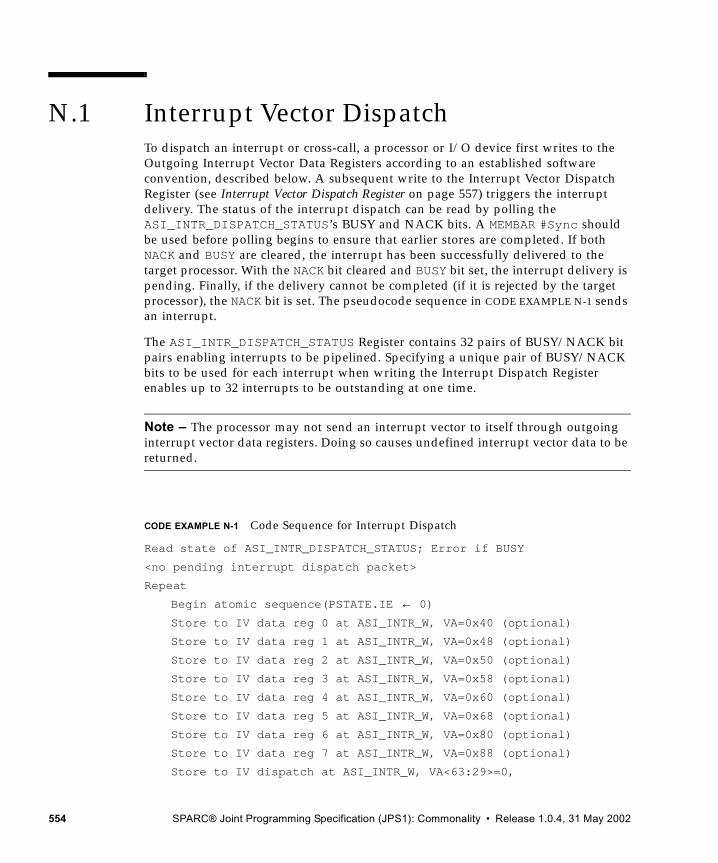
N.1 Interrupt Vector DispatchTo dispatch an interrupt or cross-call, a processor or I/O device first writes to the Outgoing Interrupt Vector Data Registers according to an established software convention, described below. A subsequent write to the Interrupt Vector Dispatch Register (see Interrupt Vector Dispatch Register on page 557) triggers the interrupt delivery. The status of the interrupt dispatch can be read by polling the ASI_INTR_DISPATCH_STATUS’s BUSY and NACK bits. A MEMBAR #Sync should be used before polling begins to ensure that earlier stores are completed. If both NACK and BUSY are cleared, the interrupt has been successfully delivered to the target processor. With the NACK bit cleared and BUSY bit set, the interrupt delivery is pending. Finally, if the delivery cannot be completed (if it is rejected by the target processor), the NACK bit is set. The pseudocode sequence in CODE EXAMPLE N-1 sends an interrupt.
The ASI_INTR_DISPATCH_STATUS Register contains 32 pairs of BUSY/NACK bit pairs enabling interrupts to be pipelined. Specifying a unique pair of BUSY/NACK bits to be used for each interrupt when writing the Interrupt Dispatch Register enables up to 32 interrupts to be outstanding at one time.
Note – The processor may not send an interrupt vector to itself through outgoing interrupt vector data registers. Doing so causes undefined interrupt vector data to be returned.
CODE EXAMPLE N-1 Code Sequence for Interrupt Dispatch
Read state of ASI_INTR_DISPATCH_STATUS; Error if BUSY
<no pending interrupt dispatch packet>
Repeat
Begin atomic sequence(PSTATE.IE ← 0)
Store to IV data reg 0 at ASI_INTR_W, VA=0x40 (optional)
Store to IV data reg 1 at ASI_INTR_W, VA=0x48 (optional)
Store to IV data reg 2 at ASI_INTR_W, VA=0x50 (optional)
Store to IV data reg 3 at ASI_INTR_W, VA=0x58 (optional)
Store to IV data reg 4 at ASI_INTR_W, VA=0x60 (optional)
Store to IV data reg 5 at ASI_INTR_W, VA=0x68 (optional)
Store to IV data reg 6 at ASI_INTR_W, VA=0x80 (optional)
Store to IV data reg 7 at ASI_INTR_W, VA=0x88 (optional)
Store to IV dispatch at ASI_INTR_W, VA<63:29>=0,
554 SPARC® Joint Programming Specification (JPS1): Commonality • Release 1.0.4, 31 May 2002
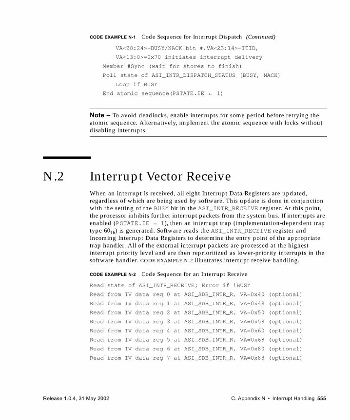
Note – To avoid deadlocks, enable interrupts for some period before retrying the atomic sequence. Alternatively, implement the atomic sequence with locks without disabling interrupts.
N.2 Interrupt Vector ReceiveWhen an interrupt is received, all eight Interrupt Data Registers are updated, regardless of which are being used by software. This update is done in conjunction with the setting of the BUSY bit in the ASI_INTR_RECEIVE register. At this point, the processor inhibits further interrupt packets from the system bus. If interrupts are enabled (PSTATE.IE = 1), then an interrupt trap (implementation-dependent trap type 6016) is generated. Software reads the ASI_INTR_RECEIVE register and Incoming Interrupt Data Registers to determine the entry point of the appropriate trap handler. All of the external interrupt packets are processed at the highest interrupt priority level and are then reprioritized as lower-priority interrupts in the software handler. CODE EXAMPLE N-2 illustrates interrupt receive handling.
VA<28:24>=BUSY/NACK bit #,VA<23:14>=ITID,
VA<13:0>=0x70 initiates interrupt delivery
Membar #Sync (wait for stores to finish)
Poll state of ASI_INTR_DISPATCH_STATUS (BUSY, NACK)
Loop if BUSY
End atomic sequence(PSTATE.IE ← 1)
CODE EXAMPLE N-2 Code Sequence for an Interrupt Receive
Read state of ASI_INTR_RECEIVE; Error if !BUSY
Read from IV data reg 0 at ASI_SDB_INTR_R, VA=0x40 (optional)
Read from IV data reg 1 at ASI_SDB_INTR_R, VA=0x48 (optional)
Read from IV data reg 2 at ASI_SDB_INTR_R, VA=0x50 (optional)
Read from IV data reg 3 at ASI_SDB_INTR_R, VA=0x58 (optional)
Read from IV data reg 4 at ASI_SDB_INTR_R, VA=0x60 (optional)
Read from IV data reg 5 at ASI_SDB_INTR_R, VA=0x68 (optional)
Read from IV data reg 6 at ASI_SDB_INTR_R, VA=0x80 (optional)
Read from IV data reg 7 at ASI_SDB_INTR_R, VA=0x88 (optional)
CODE EXAMPLE N-1 Code Sequence for Interrupt Dispatch (Continued)
Release 1.0.4, 31 May 2002 C. Appendix N • Interrupt Handling 555
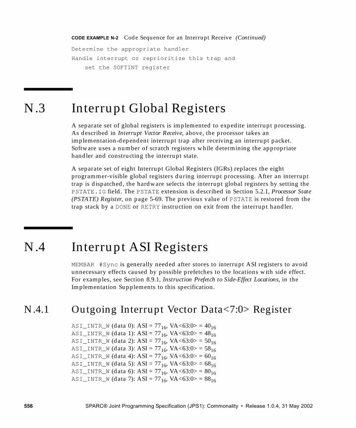
N.3 Interrupt Global RegistersA separate set of global registers is implemented to expedite interrupt processing. As described in Interrupt Vector Receive, above, the processor takes an implementation-dependent interrupt trap after receiving an interrupt packet. Software uses a number of scratch registers while determining the appropriate handler and constructing the interrupt state.
A separate set of eight Interrupt Global Registers (IGRs) replaces the eight programmer-visible global registers during interrupt processing. After an interrupt trap is dispatched, the hardware selects the interrupt global registers by setting the PSTATE.IG field. The PSTATE extension is described in Section 5.2.1, Processor State (PSTATE) Register, on page 5-69. The previous value of PSTATE is restored from the trap stack by a DONE or RETRY instruction on exit from the interrupt handler.
N.4 Interrupt ASI RegistersMEMBAR #Sync is generally needed after stores to interrupt ASI registers to avoid unnecessary effects caused by possible prefetches to the locations with side effect. For examples, see Section 8.9.1, Instruction Prefetch to Side-Effect Locations, in the Implementation Supplements to this specification.
N.4.1 Outgoing Interrupt Vector Data<7:0> RegisterASI_INTR_W (data 0): ASI = 7716, VA<63:0> = 4016ASI_INTR_W (data 1): ASI = 7716, VA<63:0> = 4816ASI_INTR_W (data 2): ASI = 7716, VA<63:0> = 5016ASI_INTR_W (data 3): ASI = 7716, VA<63:0> = 5816ASI_INTR_W (data 4): ASI = 7716, VA<63:0> = 6016ASI_INTR_W (data 5): ASI = 7716, VA<63:0> = 6816ASI_INTR_W (data 6): ASI = 7716, VA<63:0> = 8016ASI_INTR_W (data 7): ASI = 7716, VA<63:0> = 8816
Determine the appropriate handler
Handle interrupt or reprioritize this trap and
set the SOFTINT register
CODE EXAMPLE N-2 Code Sequence for an Interrupt Receive (Continued)
556 SPARC® Joint Programming Specification (JPS1): Commonality • Release 1.0.4, 31 May 2002
Name: ASI_INTR_W: Outgoing Interrupt Vector Data Registers (privileged, write-only).
TABLE N-1 describes the register field of the eight Outgoing Interrupt Vector Data Registers.
A write to these eight registers modifies the outgoing Interrupt Dispatch Data Registers.
Nonprivileged access to this register causes a privileged_action trap. An attempt to read this register causes a data_access_exception trap.
N.4.2 Interrupt Vector Dispatch RegisterASI 7716
VA<63:39> = 0VA<38:29> = SID<9:0> (see impl. dep. #246)VA<28:24> = BUSY/NACK bit pair # (BN), VA<23:14> = interrupt target identifier (ITID),VA<13:0> = 7016
Name: ASI_INTR_DISPATCH_W (interrupt dispatch) (Privileged, write-only)
TABLE N-2 describes the fields of the Interrupt Vector Dispatch Register.
A write to this ASI triggers an interrupt vector dispatch to the target CPU identified with ITID (Interrupt Target ID), using BUSY/NACK bit pair BN along with the contents of the eight Interrupt Vector Data Registers.
TABLE N-1 Outgoing Interrupt Vector Data Register Format
Bits Field Type Description
63:0 Data W Interrupt data.
TABLE N-2 Interrupt Vector Dispatch Register Format
Bits Field Type Description
VA<28:24> BN W Specifies which of the BUSY/NACK bit pairs to use for the interrupt. 016 in this field (which current software is using) selects BUSY/NACK bits ASI_INTR_DISPATCH_STATUS<1:0> for backward compatibility. 116 in this field selects BUSY/NACK bits ASI_INTR_DISPATCH_STATUS<3:2>.
VA<23:14> ITID W Interrupt Target ID. Specifies the interrupt target CPU using the BUSY/NACK bit pair BN, along with the contents of the eight Interrupt Vector Data Registers.
Release 1.0.4, 31 May 2002 C. Appendix N • Interrupt Handling 557
IMPL. DEP. #246: When the Interrupt Vector Dispatch Register is written, the source module identifier (SID) is supplied in VA<38:29>. Which, if any, of the ten VA<38:29> bits are interpreted by hardware is implementation dependent.
A read from the Interrupt Vector Dispatch Register causes a data_access_exception trap. Nonprivileged access to this register causes a privileged_action trap.
N.4.3 Interrupt Vector Dispatch Status RegisterASI 4816
VA<63:0> = 0
Name: ASI_INTR_DISPATCH_STATUS (Privileged, read-only)
TABLE N-3 describes the fields of the Interrupt Vector Dispatch Status Register.
IMPL. DEP. #243: The number of BUSY/NACK bit pairs implemented in the Interrupt Vector Dispatch Status Register is implementation dependent.
The status of up to 32 outgoing interrupts can be read from ASI_INTR_DISPATCH_STATUS BUSY/NACK bits. This register contains up to 32 pairs of BUSY/NACK bit pairs: the pair at <1:0> is referred to as pair 0, <3:2> as pair 1, and so on up to pair 31 at bits <63:62>. The VA<28:24> field of the Interrupt Dispatch Register specifies which BUSY/NACK bit pair will be used for the interrupt.
Writes to this ASI cause a data_access_exception trap. Nonprivileged access to this register causes a privileged_action trap.
N.4.4 Incoming Interrupt Vector Data<7:0>ASI_INTR_R (data 0): ASI = 7F16, VA<63:0> = 4016ASI_INTR_R (data 1): ASI = 7F16, VA<63:0> = 4816ASI_INTR_R (data 2): ASI = 7F16, VA<63:0> = 5016ASI_INTR_R (data 3): ASI = 7F16, VA<63:0> = 5816ASI_INTR_R (data 4): ASI = 7F16, VA<63:0> = 6016
TABLE N-3 Interrupt Dispatch Status Register Format
Bits Field Type Description
odd NACK R Set if interrupt dispatch has failed. Cleared at the start of every interrupt dispatch attempt; set when a dispatch has failed.
even BUSY R Set when there is an outstanding dispatch.
558 SPARC® Joint Programming Specification (JPS1): Commonality • Release 1.0.4, 31 May 2002
ASI_INTR_R (data 5): ASI = 7F16, VA<63:0> = 6816ASI_INTR_R (data 6): ASI = 7F16, VA<63:0> = 8016ASI_INTR_R (data 7): ASI = 7F16, VA<63:0> = 8816
Name: ASI_INTR_R
TABLE N-4 describes the register field of the eight Incoming Interrupt Vector Data Registers.
A read from these registers returns incoming interrupt information from the incoming Interrupt Receive Data Registers.
Nonprivileged access to this register causes a privileged_action trap.
N.4.5 Interrupt Vector Receive RegisterASI 4916
VA<63:0> = 0
Name: ASI_INTR_RECEIVE (Privileged)
TABLE N-5 describes the fields of the Interrupt Receive Register.
The status of an incoming interrupt can be read from ASI_INTR_RECEIVE. The BUSY bit is cleared by writing 0 to this register.
TABLE N-4 Incoming Interrupt Vector Data Register Format
Bits Field Type Use — Description
63:0 Data R Interrupt data.
TABLE N-5 Interrupt Receive Register Format
Bits Field Type Description
63:11 R Reserved.
10:6 SID_U R Most significant (Upper) 5 bits of the physical module ID (MID) of the interrupter. Source ID bits <9:5> of interrupter.
5 BUSY RW Set when an interrupt vector is received. The BUSY bit must be cleared by software writing 0.
4:0 SID_L R Least significant (Lower) 5 bits of the physical module ID (MID) of the interrupter.
Release 1.0.4, 31 May 2002 C. Appendix N • Interrupt Handling 559
IMPL. DEP. #247: Which, if any, of the 10 bits of the physical module ID (MID) of the interrupt source is set by hardware in the SID_U and SID_L fields of the Interrupt Vector Receive Register is implementation dependent. Also, the source of the physical module ID (MID) bits is implementation dependent.
Nonprivileged access to the Interrupt Vector Receive Register causes a privileged_action trap.
N.5 Software Interrupt Register (SOFTINT)To schedule interrupt vectors for processing at a later time, each processor can send itself signals by setting bits in the SOFTINT register.
TABLE 5-16 on page 89 describes the fields of the SOFTINT register.
The SOFTINT register (ASR 1616) is used for communication from nucleus (TL > 0) code to kernel (TL = 0) code. Interrupt packets and other service requests can be scheduled in queues or mailboxes in memory by the nucleus, which then sets SOFTINT<n> to cause an interrupt at level <n>.
Nonprivileged access to this register causes a privileged_opcode trap.
N.5.1 Setting the Software Interrupt RegisterSetting SOFTINT<n> is done by a write to the SET_SOFTINT register (ASR 1416), with bit n corresponding to the interrupt level set. The value written to the SET_SOFTINT register is effectively ORed into the SOFTINT register. This approach allows the interrupt handler to set one or more bits in the SOFTINT register with a single instruction.
Read accesses to the SET_SOFTINT register cause an illegal_instruction trap. Nonprivileged accesses to this register cause a privileged_opcode trap.
When the nucleus returns, if (PSTATE.IE = 1) and (n > PIL), then the processor will receive the highest-priority interrupt IRL<n> of the asserted bits in SOFTINT<16:0>. The processor then takes a trap for the interrupt request, and the nucleus sets the return state to the interrupt handler at that PIL and returns to TL = 0. In this manner, the nucleus can schedule services at various priorities and process them according to their priority.
560 SPARC® Joint Programming Specification (JPS1): Commonality • Release 1.0.4, 31 May 2002
N.5.2 Clearing the Software Interrupt RegisterWhen all interrupts scheduled for service at level n have been serviced, the kernel writes to the CLEAR_SOFTINT register (ASR 1516) with bit n set, to clear that interrupt. The complement of the value written to the CLEAR_SOFTINT register is effectively ANDed with the SOFTINT register. This approach allows the interrupt handler to clear one or more bits in the SOFTINT register with a single instruction.
Read accesses to the CLEAR_SOFTINT register cause an illegal_instruction trap. Nonprivileged write accesses to this register cause a privileged_opcode trap.
The timer interrupt TICK_INT and system timer interrupt STICK_INT are equivalent to SOFTINT<14> and have the same effect.
Note – To avoid a race condition between the kernel clearing an interrupt and the nucleus setting it, the kernel should examine the queue for any valid entries again after clearing the interrupt bit
TABLE N-6 summarizes the SOFTINT ASRs.
TABLE N-6 SOFTINT ASRs
ASR Value ASR Name Type Description
1416 SET_SOFTINT W Set bit(s) in Soft Interrupt Register.
1516 CLEAR_SOFTINT W Clear bit(s) in Soft Interrupt Register.
1616 SOFTINT RW Per-processor Soft Interrupt Register.
Release 1.0.4, 31 May 2002 C. Appendix N • Interrupt Handling 561

562 SPARC® Joint Programming Specification (JPS1): Commonality • Release 1.0.4, 31 May 2002
C.APPENDIX O
Reset, RED_state, and Error_state
RED_state (Reset, Error, and Debug state) is a restricted execution state reserved for processing traps that occur when TL = MAXTL − 1 and for processing hardware- and software-initiated resets.
This chapter examines RED_state in the following sections:
■ RED_state Characteristics on page 563■ Resets on page 564■ RED_state Trap Vector on page 565■ Machine States on page 565
O.1 RED_state CharacteristicsA reset or trap that sets PSTATE.RED (including a trap in RED_state) will clear the DCU Control Register, including the enable bits for I-cache, D-cache, IMMU, DMMU, and virtual and physical watchpoints. The characteristics of RED_state include the following:
■ The default access in RED_state is noncacheable, so there must be noncacheable scratch memory somewhere in the system.
■ The D-cache, watchpoints, and DMMU can be enabled by software in RED_state, but any trap will disable them again.
■ The IMMU and consequently the I-cache are always disabled in RED_state. Disabling overrides the enable bits in the DCU control register.
■ When PSTATE.RED is explicitly set by a software write, there are no side effects other than disabling the IMMU. Software must create the appropriate state itself.
■ Trap when TL = MAXTL − 1 immediately brings the processor into RED_state. In addition, trap when TL = MAXTL immediately brings the processor into error_state. Recovery from error_state, regardless of the means (impl. dep. #254), returns the processor to RED_state.
Release 1.0.4, 31 May 2002 C. Appendix O • Reset, RED_state, and Error_state 563
■ Any trap while in RED_state will cause the processor to enter error_state.
■ A SIR instruction generates an SIR trap on the local processor.
■ Trap to software-initiated reset causes an SIR trap on the processor and brings the processor into RED_state.
■ The External Reset pin generates an XIR trap, which is used for system debug.
■ The caches continue to snoop and maintain coherence if DMA or other processors are still issuing cacheable accesses.
Note – Exiting RED_state by writing 0 to PSTATE.RED in the delay slot of a JMPL is not recommended. A noncacheable instruction prefetch can be made to the JMPL target, which may be in a cacheable memory area. This condition could result in a bus error on some systems and cause an instruction access error trap. Exiting RED_state with DONE or RETRY avoids the problem.
O.2 ResetsReset priorities from highest to lowest are power-on resets (POR, hard or soft), externally initiated reset (XIR), watchdog reset (WDR), and software-initiated reset (SIR).
Please refer to Reset Traps on page 139 and Special Trap Processing on page 155. See also Section O.2 in SPARC JPS1 Implementation Supplements for implementation-specific details.
O.2.1 Externally Initiated Reset (XIR)An externally initiated reset (XIR) is sent to the processor through an external hardware pin. It causes a SPARC V9 XIR, which has a trap type 316 at physical address offset 6016. XIR has higher priority than all other resets except hard POR and soft POR.
XIR affects only one processor, rather than the entire system. Memory state, cache state, and most Control Status Register state (see TABLE O-1) are unchanged. System coherency is not guaranteed to be maintained through an XIR reset. The saved PC and nPC will only be approximate because the trap is not precise with respect to pipeline state. An XIR will reset internal pipeline state machines to free a hardware pipeline hang condition.
564 SPARC® Joint Programming Specification (JPS1): Commonality • Release 1.0.4, 31 May 2002
O.2.2 error_state and Watchdog Reset (WDR) A SPARC JPS1 processor enters error_state when a trap occurs at TL = MAXTL.
If the processor automatically exits error_state using WDR (impl. dep. #254), the processor signals itself internally to take a watchdog reset (WDR) and sets TT = 2. The WDR traps at physical address offset 4016.
WDR affects only one processor, rather than the entire system. CWP updates due to window traps that cause watchdog traps are the same as the no watchdog trap case.
O.2.3 Software-Initiated Reset (SIR)A software-initiated reset is initiated by a SIR instruction within any processor. This per-processor reset has a trap type 4 at physical address offset 8016. SIR affects only one processor, rather than the entire system.
O.3 RED_state Trap VectorWhen a SPARC V9 processor processes a reset or trap that enters RED_state, it takes a trap at an offset relative to the RED_state_trap_vector base address (RSTVaddr).
■ In SPARC V9, RSTVaddr is fixed at virtual address FFFF FFFF F000 000016.
■ RSTVaddr passes through to an implementation-dependent physical address (impl. dep. #114).
O.4 Machine StatesTABLE O-1 shows the machine states created as a result of any reset or when RED_state is entered.
TABLE O-1 Machine State After Reset and When Entering RED_state (1 of 4)
Name Fields POR WDR XIR SIR RED_state‡
Integer registers Undefined Undefined
Floating-point registers Undefined Undefined
Release 1.0.4, 31 May 2002 C. Appendix O • Reset, RED_state, and Error_state 565
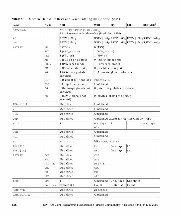
RSTVaddr VA = FFFF FFFF F000 000016PA = implementation dependent (impl. dep. #114)
PC
nPC
RSTV | 2016
RSTV | 2416
RSTV | 4016
RSTV | 4416
RSTV | 6016
RSTV | 6416
RSTV | 8016
RSTV | 8416
RSTV | A016
RSTV | A416
PSTATE MM
RED
PEF
AM
PRIV
IE
AG
CLE
TLE
IG
MG
0 (TSO)1 (RED_state)1 (FPU on)0 (Full 64-bit address1 (Privileged mode)0 (Disable interrupts)1 (Alternate globals selected)0 (Current little-endian)0 (Trap little-endian)0 (Interrupt globals not selected)0 (MMU globals not selected)
0 (TSO)1 (RED_state)1 (FPU on)0 (Full 64-bit address)1 (Privileged mode)0 (Disable interrupts)1 (Alternate globals selected)
PSTATE.TLE
Undefined0 (Interrupt globals not selected)
0 (MMU globals not selected)
TBA<63:15> Undefined Undefined
Y Undefined Undefined
PIL Undefined Undefined
CWP Undefined Undefined except for register window traps
TT[TL] 1 trap type or 2†
3 4 trap type
CCR Undefined UndefinedUndefinedASI Undefined
TL MAXTL Min(TL+1, MAXTL)
TPC[TL]
TNPC[TL]
UndefinedUndefined
PC
nPC
Impl. dep.Impl. dep
PC
nPC
TSTATE CCR
ASI
PSTATE
CWP
PC
nPC
UndefinedUndefinedUndefinedUndefinedUndefinedUndefined
CCR
ASI
PSTATE
CWP
PC
nPC
TICK NPT
counter
1Restart at 0
UndefinedCount
UndefinedRestart at 0
Undefined Count
CANSAVE Undefined Undefined
CANRESTORE Undefined Undefined
TABLE O-1 Machine State After Reset and When Entering RED_state (2 of 4)
Name Fields POR WDR XIR SIR RED_state‡
566 SPARC® Joint Programming Specification (JPS1): Commonality • Release 1.0.4, 31 May 2002
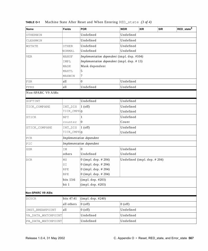
OTHERWIN Undefined Undefined
CLEANWIN Undefined Undefined
WSTATE OTHER
NORMAL
UndefinedUndefined
UndefinedUndefined
VER MANUF
IMPL
MASK
MAXTL
MAXWIN
Implementation dependent (impl. dep. #104)Implementation dependent (impl. dep. # 13)Mask dependent57
FSR all 0 Undefined
FPRS all Undefined Undefined
Non-SPARC V9 ASRs
SOFTINT Undefined Undefined
TICK_COMPARE INT_DIS
TICK_CMPR
1 (off)0
UndefinedUndefined
STICK NPT
counter
10
UndefinedCount
STICK_COMPARE INT_DIS
TICK_CMPR
1 (off)0
UndefinedUndefined
PCR Implementation dependent
PIC Implementation dependent
GSR IM
others0Undefined
UndefinedUndefined
DCR MS
SI
RPE
BPE
0 (impl. dep. # 204)0 (impl. dep. # 204)0 (impl. dep. # 204)0 (impl. dep. # 204)
Undefined (impl. dep. # 204)
bits 13:6bit 1
(impl. dep. #203)(impl. dep. #203)
Non-SPARC V9 ASIs
DCUCR bits 47:41 (impl. dep. #240)
all others 0 (off) 0 (off)
INST_BREAKPOINT all 0 (off) Undefined
VA_DATA_WATCHPOINT Undefined Undefined
PA_DATA_WATCHPOINT Undefined Undefined
TABLE O-1 Machine State After Reset and When Entering RED_state (3 of 4)
Name Fields POR WDR XIR SIR RED_state‡
Release 1.0.4, 31 May 2002 C. Appendix O • Reset, RED_state, and Error_state 567
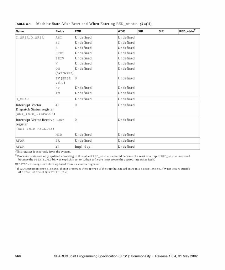
*This register is read-only from the system.‡ Processor states are only updated according to this table if RED_state is entered because of a reset or a trap. If RED_state is entered
because the PSTATE.RED bit was explicitly set to 1, then software must create the appropriate states itself.
UPDATED - this register field is updated from its shadow register.† If WDR occurs in error_state, then it preserves the trap type of the trap that caused entry into error_state. If WDR occurs outside
of error_state, it sets TT[TL] to 2.
I_SFSR, D_SFSR ASI
FT
E
CTXT
PRIV
W
OW (overwrite)FV (SFSR valid)NF
TM
UndefinedUndefinedUndefinedUndefinedUndefinedUndefinedUndefined
0
UndefinedUndefined
UndefinedUndefinedUndefinedUndefinedUndefinedUndefinedUndefined
Undefined
UndefinedUndefined
D_SFAR Undefined Undefined
Interrupt Vector Dispatch Status register (ASI_INTR_DISPATCH)
all 0 Undefined
Interrupt Vector Receive register (ASI_INTR_RECEIVE)
BUSY 0 Undefined
MID Undefined Undefined
AFAR PA Undefined Undefined
AFSR all Impl. dep. Undefined
TABLE O-1 Machine State After Reset and When Entering RED_state (4 of 4)
Name Fields POR WDR XIR SIR RED_state‡
568 SPARC® Joint Programming Specification (JPS1): Commonality • Release 1.0.4, 31 May 2002
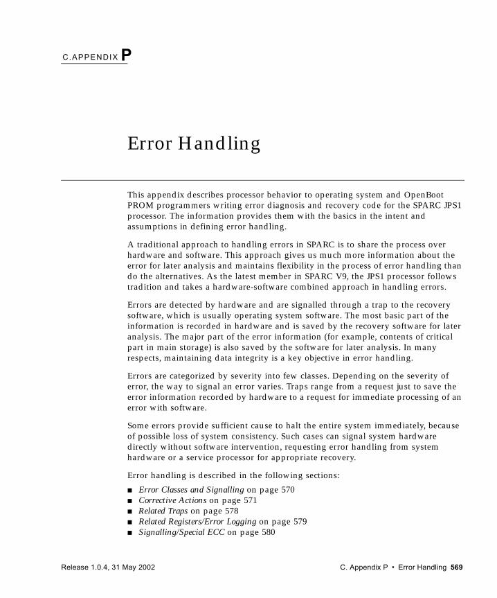
C.APPENDIX P
Error Handling
This appendix describes processor behavior to operating system and OpenBoot PROM programmers writing error diagnosis and recovery code for the SPARC JPS1 processor. The information provides them with the basics in the intent and assumptions in defining error handling.
A traditional approach to handling errors in SPARC is to share the process over hardware and software. This approach gives us much more information about the error for later analysis and maintains flexibility in the process of error handling than do the alternatives. As the latest member in SPARC V9, the JPS1 processor follows tradition and takes a hardware-software combined approach in handling errors.
Errors are detected by hardware and are signalled through a trap to the recovery software, which is usually operating system software. The most basic part of the information is recorded in hardware and is saved by the recovery software for later analysis. The major part of the error information (for example, contents of critical part in main storage) is also saved by the software for later analysis. In many respects, maintaining data integrity is a key objective in error handling.
Errors are categorized by severity into few classes. Depending on the severity of error, the way to signal an error varies. Traps range from a request just to save the error information recorded by hardware to a request for immediate processing of an error with software.
Some errors provide sufficient cause to halt the entire system immediately, because of possible loss of system consistency. Such cases can signal system hardware directly without software intervention, requesting error handling from system hardware or a service processor for appropriate recovery.
Error handling is described in the following sections:
■ Error Classes and Signalling on page 570■ Corrective Actions on page 571■ Related Traps on page 578■ Related Registers/Error Logging on page 579■ Signalling/Special ECC on page 580
Release 1.0.4, 31 May 2002 C. Appendix P • Error Handling 569
P.1 Error Classes and SignallingAn error is categorized according to its severity and its characteristics with respect to instruction execution.
P.1.1 Error Classes in SeverityThe classes of error in order of severity are as follows:
1. Hardware-corrected errors. Hardware tries to correct the error automatically. A trap is optionally generated to log the error conditions when the error is corrected to enable the actions for preventive maintenance. Upon failure to correct the error, the processor could invoke a trap requesting software recovery.
2. Software-correctable errors. Hardware does not correct the error automatically. Instead, it invokes a trap requesting the recovery software to correct the error. Corrective actions are expected from the recovery software. If recovery is successful, the system should continue the operation.
3. Uncorrectable errors. The error is by its nature uncorrectable, and hardware invokes a trap to signal the occurrence of the error to appropriate recovery software. Depending on the condition under which the error occurs, the system may be able to recover from the error and continue operation. If not, it may be able to isolate the error to a particular process and terminate it. Otherwise, the software should shut down the system gracefully.
4. Fatal errors. By its nature, the error indicates either loss of system consistency or a system interconnect protocol error. It is dangerous to continue operation in this situation because of the impending threat of a failure to maintain data integrity. Therefore, upon the detection of the error, the processor generates an ERROR signal to its interconnect, expecting to be halted/reset by the system. System actions induced by the ERROR signal are system-implementation-dependent.
P.1.2 Errors Asynchronous to Instruction ExecutionSome errors can be detected asynchronously to instruction execution; other errors are detected in the course of an instruction execution.
An error asynchronous to instruction execution is signalled either through a disrupting trap to the processor or through an ERROR signal to system hardware to induce a system reset, depending on the severity of the error.
570 SPARC® Joint Programming Specification (JPS1): Commonality • Release 1.0.4, 31 May 2002
The errors signalled through a disrupting trap do not directly affect the result of programs, and it is difficult to locate programs affected by the error without any visible effect. Therefore, the actions in response to the errors asynchronous to instruction execution are to save the error information for preventive maintenance.
Errors signalled with an ERROR are meant either to be loss of system consistency or a protocol error on system interconnect.
On the other hand, an error detected in the course of an instruction execution is signalled through an error trap to the instruction, with additional information recorded in hardware. The trap is either precise or deferred. The program (process) affected by the error should be given a corrected response, or if the error is uncorrectable, the process should be terminated appropriately.
IMPL. DEP. #208: The order in which errors are captured in instruction execution is implementation dependent in SPARC JPS1. Ordering could be in program order or in the order of detection.
Note – Both hardware and software must take special care in handling a deferred trap invoked with an error. Hardware must record the state information of the privileged_mode bit (PSTATE.PRIV) either upon detection of the error or upon execution of the instruction that encounters the error. Software must insert an error barrier at the environmental boundary to make valid the privileged/nonprivileged status information recorded by hardware.
P.2 Corrective ActionsErrors are handled by invocation of one of the following actions:
■ Reset-inducing ERROR signal. A fatal error generates an ERROR signal to induce a system reset. Both an error detected in the course of instruction execution and an error asynchronous to instruction execution may generate an ERROR signal (impl. dep. #212).
■ Precise traps. Either a software-correctable error or an uncorrectable error generates a precise trap to request software to intervene before normal processor execution continues. An error detected in the course of an instruction execution generates this type of trap.
■ Deferred traps. An uncorrectable error requiring immediate attention generates a deferred trap to request software intervention. The recovery software examines the recorded error information to determine the extent of the damage caused by the error. Depending on the observed effect, the system may need to be brought
Release 1.0.4, 31 May 2002 C. Appendix P Error Handling 571
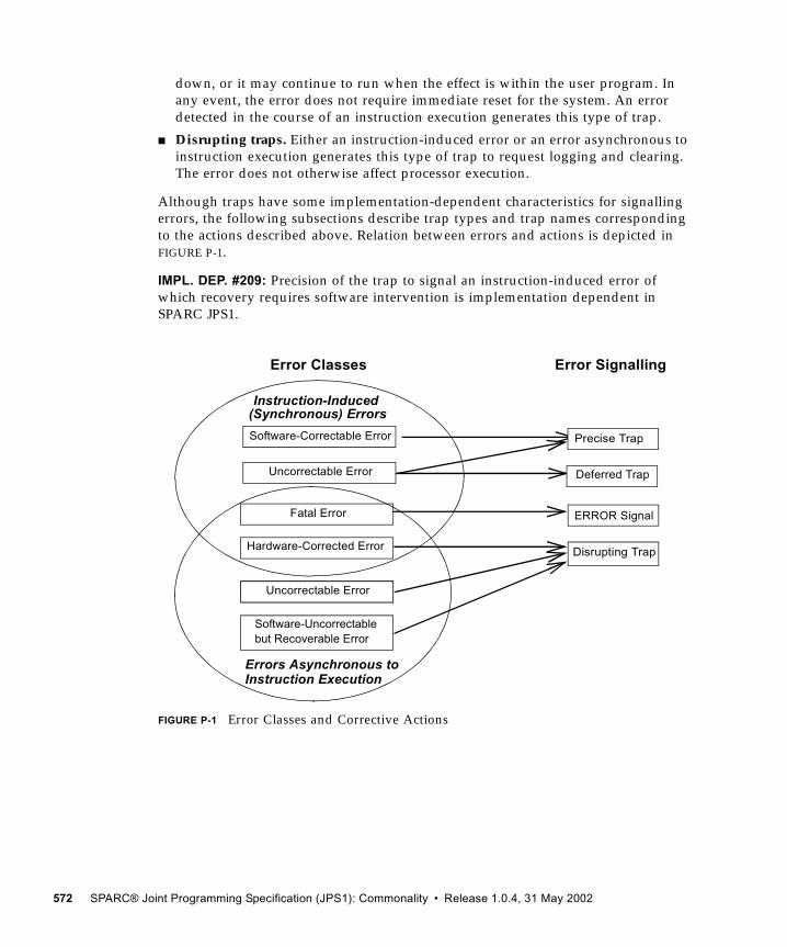
down, or it may continue to run when the effect is within the user program. In any event, the error does not require immediate reset for the system. An error detected in the course of an instruction execution generates this type of trap.
■ Disrupting traps. Either an instruction-induced error or an error asynchronous to instruction execution generates this type of trap to request logging and clearing. The error does not otherwise affect processor execution.
Although traps have some implementation-dependent characteristics for signalling errors, the following subsections describe trap types and trap names corresponding to the actions described above. Relation between errors and actions is depicted in FIGURE P-1.
IMPL. DEP. #209: Precision of the trap to signal an instruction-induced error of which recovery requires software intervention is implementation dependent in SPARC JPS1.
FIGURE P-1 Error Classes and Corrective Actions
(Synchronous) Errors
Precise Trap
Deferred Trap
Disrupting Trap
ERROR Signal
Hardware-Corrected Error
Software-Correctable Error
Errors Asynchronous to Instruction Execution
Error Classes Error Signalling
Uncorrectable Error
Fatal Error
Uncorrectable Error
Uncorrectable Error
Software-Uncorrectablebut Recoverable Error
Instruction-Induced
572 SPARC® Joint Programming Specification (JPS1): Commonality • Release 1.0.4, 31 May 2002
P.2.1 Reset-Inducing ERROR SignalIt is usually impossible to recover a system or a coherence domain that suffers loss of system or domain coherency because of various error conditions in caches or in the system interconnect that carries coherency transactions. The characteristic examples of such error conditions are an interconnect address error and an error in E-cache tag status information.
Upon the detection of an error condition that indicates loss of system or domain coherency, the system or processor tries to stop everything to maintain data integrity by shutting down the system or domain as soon as possible. The error class that indicates loss of system/domain coherence is called fatal error, as defined in the preceding section. When a fatal error is detected by a processor, the processor asserts its ERROR output signal to system hardware. Although the processor expects the system to generate a system reset for entire system or coherence domain in response to the ERROR output signal, the actual response of the system when it receives an ERROR signal depends on the system design.
IMPL. DEP. #210: The following aspects of the ERROR output signal are implementation dependent in SPARC JPS1:
■ The causes of the ERROR signal■ Whether each of the causes of the ERROR signal, when it generates the ERROR
signal, halts the processor or allows the processor to continue running■ The exact semantics of the ERROR signal
For exact definitions of the causes and semantics of the ERROR output signal, please refer to individual JPS1 Implementation Supplements.
To provide basic information for fault analysis on a fatal error, the processor preserves some part of the contents of error logging registers beyond the system/domain reset induced by the ERROR signal. For the definitions of machine states after reset, please refer to Appendix O, Reset, RED_state, and Error_state, of JPS1 Implementation Supplements.
The expected scenario is as follows:
After the system/domain reset in response to an ERROR signal, system/domain initialization software takes charge of system recovery. During the system initialization process, the software examines error logging registers to locate the source of the reset and the cause of the fatal error. The software further saves the information, including the contents of error logging registers, to provide later fault analysis with as much information as possible.
IMPL. DEP. #211: The information that the error logging registers preserves beyond the reset induced by an ERROR signal is implementation dependent in SPARC JPS1.
Release 1.0.4, 31 May 2002 C. Appendix P Error Handling 573
Although most fatal errors that lead to an assertion of ERROR signal do not cause any special processor behavior, in some cases, depending on the implementation, there are a few fatal errors for which the processor asserts an ERROR signal and begins a trap execution.
IMPL. DEP. #212: Generation of a trap along with assertion of an ERROR signal upon detection of a fatal error is implementation dependent in SPARC JPS1.
P.2.2 Precise TrapsA precise trap occurs before any program-visible state has been modified by the instruction to which the TPC points. When a precise trap occurs, several conditions are true:
1. The PC saved in TPC[TL] points to the instruction that induced the trap and the nPC saved in TNPC[TL] points to the instruction that was to be executed next.
2. All instructions issued before the instruction pointed to by the TPC have completed execution.
3. Any instructions issued after the instruction pointed to by the TPC remain unexecuted.
A precise trap is invoked when a software-correctable error or an uncorrectable error is detected. By its definition, a precise trap is only generated with an error detected in the course of an instruction execution.
A precise trap is signalled when an error that needs software intervention for recovery is detected. Depending on the condition under which the error occurs, the system may be able to recover from the error and continue operation. If not, it may be able to isolate the error to a particular process and terminate it. Otherwise, the software should shut down the system gracefully. State information saved in the trap stack can help the software error handler identify the privileged state under which the error is detected.
P.2.3 Deferred TrapsDepending on the implementation of instruction execution control, there may be cases in which completion of instruction execution is out of its program order. If an error is detected in the course of such instruction, the error is signalled with a deferred trap. Deferred traps may corrupt the processor state. Such traps lead to termination of the currently executing process or result in a system shutdown if the system state has been corrupted. Error logging information allows software to determine if system state has been corrupted.
574 SPARC® Joint Programming Specification (JPS1): Commonality • Release 1.0.4, 31 May 2002
In SPARC JPS1 processors, the privileged state information related to the error is logged into one of the error status registers. A bit in the error status register indicates the privileged state of the processor, either when it detects the error or when it executes the instruction that encounters the error. For details, refer to the Implementation Supplements.
Note – In SPARC JPS1, Asynchronous Fault Status Register (AFSR) may contain a bit to indicate the privileged state bit (AFSR.PRIV) associated with the error.
IMPL. DEP. #213: The existence of the AFSR.PRIV bit is implementation dependent. If AFSR.PRIV is implemented, it is implementation dependent whether the logged AFSR.PRIV indicates the privileged state upon the detection of an error or upon the execution of an instruction that induces the error. For the former implementation to be effective, operating software must provide error barriers appropriately.
See Error Barriers, below, for more information.
IMPL. DEP. #214: Whether an implementation provides an enable/disable control feature for deferred traps is implementation dependent in SPARC JPS1.
Error Barriers
A MEMBAR #Sync instruction provides an error barrier for deferred traps. It ensures that deferred traps from earlier memory references are not reported after the MEMBAR. To provide error isolation between processes, use a MEMBAR #Sync when context switching or whenever the error logging information that identifies AFSR.PRIV bit is changed. Note that traps do not provide the same function as MEMBAR #Sync.
IMPL. DEP. #215: DONE and RETRY instructions may implicitly provide an error barrier function as MEMBAR #Sync. Whether DONE and RETRY instructions provide an error barrier is implementation dependent in SPARC JPS1.
TPC, TNPC, and Deferred Traps
After a deferred trap, the contents of TPC[TL] and TNPC[TL] are undefined. They do not generally contain the oldest nonexecuted instruction and its next PC. Because of this, execution cannot normally be resumed from the point that the trap is taken.
Deferred Trap Handler Functionality
The following is a possible sequence to handle an error signalled through a deferred trap. In this sequence, a pair of error logging registers—an error status register and an error address register—is assumed as described above.
1. Log the error(s).
Release 1.0.4, 31 May 2002 C. Appendix P Error Handling 575
2. Reset the error logging bits in the error status register. Perform a MEMBAR #Sync to complete internal state changes.
3. Panic if the error occurs under privileged state not performing an intentional peek/poke (See Special Access Sequence for Recovering Deferred Traps on page 576); otherwise, try to continue.
4. Validate the faulty location, if required, based on the information logged.
5. Abort the current process.
6. For user-process uncorrectable errors in a conventional UNIX system, once all processes using the physical page in error have been signalled and terminated, as part of the normal page recycling mechanism, clear the uncorrectable error from main memory by zeroing the page, using block store instructions.
7. Resume execution.
Special Access Sequence for Recovering Deferred Traps
A special access sequence is required for intentional peeks and pokes to determine device presence and correctness, and for I/O accesses from hardened drivers that must survive faults in an I/O device. This special access sequence allows the error trap handler to recover predictably, even though the trap is deferred. One possible sequence is described here.
The procedure is for an error signalled for data reference, meaning that the sequence is executed in a data_access_error trap handler.
The_peeker: <set a flag indicating special peek sequence is about tooccur. This flag includes specifying the handler as aSpecial_peek_handler if a deferred TO/BERR does occur>
MEMBAR #Sync /* error barrier for deferred traps, [1] see explanation below*/
<call routine to do the peek>
<reset the peek_sequence>
<check success/failure indication from peek>
Do_the_peek_routine: <perform load. If deferred trap occurs, execution will neverresume here>
MEMBAR #Sync /* error barrier; make sure load takes */
<indicate peek success>
<return to peeker>
576 SPARC® Joint Programming Specification (JPS1): Commonality • Release 1.0.4, 31 May 2002
Special_peek_handler: <indicate peek failure>
<return to peeker as if returning from Do_the_peek_routine>
Deferred_trap_handler: (TL = 1) <If the deferred trap handler sees a UE or TO or BERR and
the peek_sequence_flag is set, it resumes execution at theSpecial_peek_handler (by setting TPC and TNPC)>
Other than the load (or store, in the case of poke), Do_the_peek_routine should not have any other side effect since the deferred trap means that the code is not restartable. Execution after the trap is resumed in Special_peek_handler.
The code in Deferred_trap_handler must be able to recognize any deferred traps that happen as a result of hitting the error barrier in The_peeker as not being from the peek operation. This will typically be part of setting the peek_sequence_flag.
A MEMBAR #Sync is required as the first instruction in the trap table entry for Deferred_trap_handler to collect all potential trapping stores together to avoid a RED_state exception (see Error Barriers on page 575).
TPC or AFAR can be used to identify whether a deferred trap came from a peek or poke sequence. If TPC is used, the locality of the trap to Do_the_peek_routine must be ensured by use of an error barrier, as in the example above. If AFAR is used, the presence of orphaned errors, resulting from the asynchronous activity of the instruction fetcher, must be considered. If an orphaned error occurs, then the source of the TO or BERR report cannot be determined from the AFAR. Given the error barrier sequence above, it is reasonable to expect that the TO or BERR resulted from the peek or poke and to proceed accordingly. To reduce the likelihood of this event, orphaned errors could be cleaned at point [1] above. The source of the TO or BERR could be confirmed by retrying the peek or poke: If the TO or BERR happens again, the system can continue with the normal peek or poke failure case. If the TO or BERR does not happen, the system must panic.
The peek access should be preceded and followed by MEMBAR #Sync instructions. The destination register of the access may be destroyed, but no other state will be corrupted. If TPC points to the MEMBAR #Sync following the access, then the trap handler knows that a recoverable error has occurred and resumes execution after setting a status flag. The trap handler must set TNPC to TPC + 4 before resuming because the contents of TNPC are otherwise undefined.
P.2.4 Disrupting TrapsDisrupting traps, like deferred traps, may have changed their program-visible state since the instruction that caused them. The following are true for a disrupting trap:
Release 1.0.4, 31 May 2002 C. Appendix P Error Handling 577
1. The PC saved in TPC[TL] points to a valid instruction that will be executed by the program, and the nPC saved in TNPC[TL] points to the instruction that will be executed after that one.
2. All instructions issued before the one pointed to by the TPC have completed execution.
3. Any instructions issued after the one pointed to by the TPC remain unexecuted.
Errors that lead to disrupting traps are hardware-corrected errors and uncorrectable errors. A hardware-corrected error in the course of an instruction execution, an uncorrectable error, or a hardware-corrected error triggered with an asynchronous event may cause a disrupting trap.
The disrupting trap handler should save the information on the error logged in error status registers. No special operations such as cache flushing are required for correctness after a disrupting trap. However, for many errors, it is appropriate to correct the data that produced the original error so that later references to the same faulty data do not produce the same trap again. For uncorrectable errors, software must determine the recovery mechanism with the minimum system impact.
For hardware-corrected errors, SPARC JPS1 implementations should provide a mechanism to enable and disable traps for software error handling. In some cases, software disables these disrupting traps and only reads the logging information periodically to gather error statistics for later preventive maintenance.
Note – To prevent multiple traps from the same error, software should not reenable interrupts until after the disrupting error status bit in AFSR is cleared.
P.3 Related TrapsSPARC JPS1 processors use the following traps for error signalling:
■ data_access_error [tt = 3216]: An error, either precise or deferred, detected during execution of data reference. The error is detected in the course of a memory reference instruction execution.
■ instruction_access_error [tt = 0A16]: An error, either precise or deferred, detected during instruction fetch reference. The error is detected in the course of an instruction fetch reference.
■ ECC_error [tt = 6316]: A disrupting trap. Either an error corrected automatically by hardware or an uncorrectable error. Both an instruction-inducing error and an error asynchronous to instruction execution are possible.
578 SPARC® Joint Programming Specification (JPS1): Commonality • Release 1.0.4, 31 May 2002
IMPL. DEP. #216: The precision of a data_access_error trap is implementation dependent in SPARC JPS1.
IMPL. DEP. #217: The precision of an instruction_access_error trap is implementation dependent in SPARC JPS1.
The followings traps are used in SPARC JPS1 processors as JPS1 implementation-dependent traps. See the Implementation Supplement for details.
■ fast_ECC_error [tt = 7016]: A precise trap for the system to be able to continue operation. A single-bit or multiple-bit ECC error is detected (impl. dep. #202).
■ async_data_error [tt = 4016]: An implementation-dependent trap (impl. dep. #31, #218) that signifies an urgent error, to be processed as soon as possible. Precise, deferred, or disrupting. When async_data_error is not precise, the TPC and TNPC stacked by the trap are not necessarily related to the instruction or data access that caused the error.
IMPL. DEP. #218: Whether async_data_error trap is implemented is implementation dependent. If it does exist, it indicates that an error is detected in a processor core and its trap type is 4016.
P.4 Related Registers/Error LoggingAlthough the SPARC JPS1 processor contains some error logging registers, information about an error is always recorded in a pair of error logging registers: an error status register to identify causes of error, and an error address register to get address information for an error. Therefore, the amount of information for an error does not exceed two 64-bit words. Note that an error status register and an error address register do not mean a single entity each. Rather, they mean one of multiple status registers and one of multiple address registers paired to the status register. In each error condition, the valid pair of error logging register varies, for convenience in software error handling.
In addition, for instruction-related errors signalled as an instruction_access_error trap, address information is provided in TPC[TL], not in an explicit logging register.
The following registers are provided in the SPARC JPS1 processor for error handling:
■ Instruction Synchronous Fault Status Register (ISFSR: ASI = 5016, VA = 1816)
■ Data Synchronous Fault Status Register (DSFSR: ASI = 5816, VA = 1816)
■ Data Synchronous Fault Address Register (DSFAR: ASI = 5816, VA = 2016)
■ Asynchronous Fault Status Register (AFSR: ASI = 4C16, VA = 016)
■ Asynchronous Fault Address Register (AFAR: ASI = 4D16, VA = implementation dependent)
Release 1.0.4, 31 May 2002 C. Appendix P Error Handling 579
IMPL. DEP. #219: Allocation of Asynchronous Fault Address Register (AFAR) is implementation dependent in SPARC JPS1. There may be one instance or multiple instances of AFAR. Although the ASI for AFAR is defined as 4D16, the virtual address of AFAR if there are multiple AFARs is implementation dependent in SPARC JPS1.
IMPL. DEP. #220: Whether the implementation supports additional logging/control registers for error handling is implementation dependent in SPARC JPS1.
Note that an error signalled through a precise trap may be logged in AFSR/AFAR pair, whereas an error signalled through a deferred trap is never logged in a synchronous status/address register pair. For details about error logging mechanisms, refer to the appropriate Implementation Supplement.
These error status and error address registers may be overwritten with subsequent error(s) depending on the implementation. For overwriting policies, refer to the appropriate Implementation Supplement.
P.5 Signalling/Special ECCThe SPARC JPS1 processor provides a special feature for memory-related errors. The feature is called as signalling ECC or special ECC, depending on the implementation. This feature aids in survival and diagnosis of an error in a coherent domain; it avoids misprocessing of bad memory data.
If bad data is replaced with a good data upon detection of an error, the other processes that share the data could continue processing without knowledge of erroneous data even if they receive replaced data. To prevent the use of “fixed” faulty data, the SPARC JPS1 processor replaces the data that has a bad ECC code with an uncorrectable ECC error generated in a predetermined method. In addition to preventing the use of faulty data, the signalling/special ECC may be used for locating the faulty component in a system by embedding module ID code into the replaced data.
For details, refer to the appropriate Implementation Supplement.
IMPL. DEP. #221: The method to generate “special” or “signalling” ECCs and whether processor-ID is embedded into the data associated with special/signalling ECCs is implementation dependent in SPARC JPS1.
580 SPARC® Joint Programming Specification (JPS1): Commonality • Release 1.0.4, 31 May 2002
C.APPENDIX Q
Performance Instrumentation
For implementation-dependent performance instrumentation information, please refer to Appendix Q in specific SPARC JPS1 Implementation Supplements.
Release 1.0.4, 31 May 2002 C. Appendix Q • Performance Instrumentation 581

582 SPARC® Joint Programming Specification (JPS1): Commonality • Release 1.0.4, 31 May 2002
Bibliography
General ReferencesBoney, Joel. “SPARC Version 9 Points the Way to the Next Generation RISC,” SunWorld,October 1992, pp. 100-105.
Cohen, D., “On Holy Wars and a Plea for Peace.” Computer 14:10, October 1981, pp. 48-54.
Comer, Douglas. “The Ubiquitous B-Tree.” ACM Computing Surveys, Vol. 11, No. 2, June1979.
Implementation Characteristics of Current SPARC V9-based Products, Revision 9.x, SPARC International, Inc.
Knuth, Donald. The Art of Computer Programming, Volume 3, Searching and Sorting. Addi-son-Wesley, 1974.
Weaver, David L., editor. The SPARC Architecture Manual, Version 8, Prentice-Hall, Inc.,1992.
Weaver, David L., and Tom Germond, eds. The SPARC Architecture Manual-Version 9,Prentice-Hall, Inc., 1994.
Release 1.0.4, 31 May 2002 C. Bibliography • 583

584 SPARC® Joint Programming Specification (JPS1): Commonality • Release 1.0.4, 31 May 2002
Index
Aa field of instructions 104, 206, 209, 210, 214, 356,
359accrued exception (aexc) field of FSR register 60, 61,
63, 141, 392, 400ADD instruction 192, 485ADDC instruction 192ADDcc instruction 192, 325, 485ADDCcc instruction 192address
64-bit virtual data watchpoint 95aliased 171aliasing 439memory 171operand syntax 481physical 171physical address data watchpoint 96space identifier (ASI) 171, 537virtual 171virtual address
data watchpoint 95watchpoint priority 95
virtual passed to physical 93address mask (AM) field of PSTATE register 73address space 5address space identifier (ASI)
accessing MMU registers 458affected by watchpoint traps 94alternate address spaces, privileged/
nonprivileged 534appended to memory address 21, 102architecturally specified 174bit 7 setting for privileged_action exception 334
bypass 9, 94, 538definition 9encoding address space information 107explicit values 112imm_asi instruction field 105implicit values 112load floating-point instructions 243load from TLB Data Access register 462load from TLB Data In register 462load from TLB Tag Read register 462load integer doubleword instructions 366load integer instructions 248nontranslating 13, 94operations 452, 457with prefetch instructions 305restricted 174, 452, 538restriction indicator 67SPARC V9 address 173unrestricted 174, 505, 538
address space identifier (ASI) registerfor load/store alternate instructions 68and imm_asi instruction field 112and LDDA instruction 367and LDSTUBA instruction 254load floating-point from alternate space
instructions 244load integer from alternate space instructions 250with prefetch instructions 305for register-immediate addressing 174restoring saved state 217saved trap state 503saving state 131state after reset 566and STDA instruction 379
Release 1.0.4, 31 May 2002 C. Index 1
store floating-point into alternate space instructions 334
store integer to alternate space instructions 339and SWAPA instruction 383after trap 25and TSTATE Register 77and write state register instructions 351
addressing conventions 108addressing modes 5ADDX instruction (SPARC V8) 193ADDXcc instruction (SPARC V8) 193AFAR, See Asynchronous Fault Address Register
(AFAR)AFSR, See Asynchronous Fault Status Register
(AFSR)alias
address 171floating-point registers 48
ALIGNADDRESS instruction 194ALIGNADDRESS_LITTLE instruction 194alignment
data (load/store) 21, 108, 173doubleword 21, 108, 173extended-word 108halfword 21, 108, 173instructions 21, 108, 173integer registers 365, 367, 548maintaining 491memory 164, 173quadword 21, 108, 173stack pointer 491word 21, 108, 173
alternate address space 305alternate global registers 20, 40, 42, 503alternate globals enable (AG) field of PSTATE
register 42, 74alternate space instructions 22, 67, 534ancillary state registers (ASRs) 83–91
access 48adding instructions to SPARC V9 509assembly language syntax 476I/O register access 22I/U control/status 46number 83possible registers included 315, 352privileged 400reading/writing implementation-dependent
processor registers 400writing to 351
AND instruction 259ANDcc instruction 259, 485ANDN instruction 259, 486ANDNcc instruction 259annul bit
in branch instructions 206in conditional branches 357in control transfer instruction 47
annulled branches 206application program 9, 67, 99, 532, 534architectural extensions 509architecture, meaning for SPARC V9 1arguments to a subroutine 488arithmetic overflow 55ARRAY16 instruction 196ARRAY32 instruction 196ARRAY8 instruction 196ASI, See address space identifier (ASI)ASI_AFAR 540ASI_AFSR 540ASI_AIUP 539ASI_AIUPL 539ASI_AIUS 539ASI_AIUSL 539ASI_AS_IF_USER_PRIMARY 174, 503, 539ASI_AS_IF_USER_PRIMARY_LITTLE 174, 503, 539ASI_AS_IF_USER_SECONDARY 174, 539ASI_AS_IF_USER_SECONDARY_LITTLE 174, 539ASI_ASYNC_FAULT_ADDR 540ASI_ASYNC_FAULT_STATUS 540ASI_ATOMIC_QUAD_LDD_PHYS 540ASI_ATOMIC_QUAD_LDD_PHYS_LITTLE 540ASI_BARRIER_SYNCH 545ASI_BARRIER_SYNCH_P 542ASI_BLK_AIUP 542ASI_BLK_AIUPL 542ASI_BLK_AIUS 542ASI_BLK_AIUSL 543ASI_BLK_COMMIT_P 545ASI_BLK_COMMIT_S 545ASI_BLK_P 545ASI_BLK_PL 545ASI_BLK_S 545ASI_BLK_SL 545ASI_BLOCK_AS_IF_USER_PRIMARY 542ASI_BLOCK_AS_IF_USER_PRIMARY_LITTLE 542ASI_BLOCK_AS_IF_USER_SECONDARY 542ASI_BLOCK_AS_IF_USER_SECONDARY_LITTLE
543
2 C. Index SPARC® Joint Programming Specification (JPS1): Commonality • Release 1.0.4, 31 May 2002
ASI_BLOCK_COMMIT_PRIMARY 545ASI_BLOCK_COMMIT_SECONDARY 545ASI_BLOCK_PRIMARY 545ASI_BLOCK_PRIMARY_LITTLE 545ASI_BLOCK_SECONDARY 545ASI_BLOCK_SECONDARY_LITTLE 545ASI_DCU_CONTROL_REGISTER 92, 540ASI_DCUCR 540ASI_DEVICE_ID+SERIAL_ID 546ASI_DMMU 541ASI_DMMU_DEMAP 542ASI_DMMU_PA_WATCHPOINT_REG 541ASI_DMMU_SFAR 541ASI_DMMU_SFSR 541ASI_DMMU_TAG_ACCESS 541ASI_DMMU_TAG_TARGET_REG 541ASI_DMMU_TSB_64KB_PTR_REG 541ASI_DMMU_TSB_8KB_PTR_REG 541ASI_DMMU_TSB_BASE 541ASI_DMMU_TSB_DIRECT_PTR_REG 541ASI_DMMU_TSB_NEXT_REG 541ASI_DMMU_TSB_PEXT_REG 541ASI_DMMU_TSB_SEXT_REG 541ASI_DMMU_VA_WATCHPOINT_REG 541ASI_DTLB_DATA_ACCESS_REG 542ASI_DTLB_DATA_IN_REG 542ASI_DTLB_TAG_READ_REG 542ASI_FL16_P 544ASI_FL16_PL 545ASI_FL16_PRIMARY 544ASI_FL16_PRIMARY_LITTLE 545ASI_FL16_S 544ASI_FL16_SECONDARY 544ASI_FL16_SECONDARY_LITTLE 545ASI_FL16_SL 545ASI_FL8_P 544ASI_FL8_PL 544ASI_FL8_PRIMARY 544ASI_FL8_PRIMARY_LITTLE 544ASI_FL8_S 544ASI_FL8_SECONDARY 544ASI_FL8_SECONDARY_LITTLE 545ASI_FL8_SL 545ASI_IIU_INST_TRAP 542, 548ASI_IMMU 540ASI_IMMU_DEMAP 541ASI_IMMU_SFSR 540ASI_IMMU_TAG_TARGET 540ASI_IMMU_TSB_64KB_PTR_REG 540
ASI_INTR_DATA0_R 543ASI_INTR_DATA0_W 542ASI_INTR_DATA1_R 543ASI_INTR_DATA1_W 542ASI_INTR_DATA2_R 543ASI_INTR_DATA2_W 542ASI_INTR_DATA3_R 543ASI_INTR_DATA3_W 542ASI_INTR_DATA4_R 543ASI_INTR_DATA4_W 542ASI_INTR_DATA5_R 543ASI_INTR_DATA5_W 542ASI_INTR_DATA6_R 543ASI_INTR_DATA6_W 542ASI_INTR_DATA7_R 543ASI_INTR_DATA7_W 542ASI_INTR_DISPATCH 568ASI_INTR_DISPATCH_STATUS 554, 557, 558ASI_INTR_DISPATCH_STATUS.BUSY bit 554ASI_INTR_DISPATCH_STATUS.NACK bit 554ASI_INTR_DISPATCH_W 542, 557ASI_INTR_RECEIVE 540, 555, 559, 568ASI_INTR_W 554, 557ASI_ITLB_DATA_ACCESS_REG 541ASI_ITLB_DATA_IN_REG 541ASI_ITLB_TAG_READ_REG 541ASI_MONDO_RECEIVE_CTRL 540ASI_MONDO_SEND_CTRL 540ASI_N 539ASI_NL 539ASI_NUCLEUS 454, 539ASI_NUCLEUS_LITTLE 454, 539ASI_NUCLEUS_QUAD_LDD 547ASI_NUCLEUS_QUAD_LDD_L 540ASI_NUCLEUS_QUAD_LDD_LITTLE 540, 547ASI_P 543ASI_PHYS_BYPASS_EC_WITH_EBIT 456, 539, 546ASI_PHYS_BYPASS_EC_WITH_EBIT_L 539ASI_PHYS_BYPASS_EC_WITH_EBIT_LITTLE 539,
547ASI_PHYS_USE_EC 539, 546ASI_PHYS_USE_EC_L 539ASI_PHYS_USE_EC_LITTLE 539, 547ASI_PL 543ASI_PNF 543ASI_PNFL 543ASI_PRIMARY 112, 174, 454, 543ASI_PRIMARY_* 454ASI_PRIMARY_CONTEXT_REG 541
Release 1.0.4, 31 May 2002 C. Index 3
ASI_PRIMARY_LITTLE 71, 174, 454, 543ASI_PRIMARY_NO_FAULT 468, 543ASI_PRIMARY_NO_FAULT_LITTLE 468, 543ASI_PRIMARY_NOFAULT 174, 175ASI_PST16_P 282, 544ASI_PST16_PL 282, 544ASI_PST16_PRIMARY 544ASI_PST16_PRIMARY_LITTLE 544ASI_PST16_S 282, 544ASI_PST16_SECONDARY 544ASI_PST16_SECONDARY_LITTLE 544ASI_PST16_SL 282ASI_PST32_P 282, 544ASI_PST32_PL 282, 544ASI_PST32_PRIMARY 544ASI_PST32_PRIMARY_LITTLE 544ASI_PST32_S 282, 544ASI_PST32_SECONDARY 544ASI_PST32_SECONDARY_LITTLE 544ASI_PST32_SL 282, 544ASI_PST8_P 282, 543ASI_PST8_PL 282, 544ASI_PST8_PRIMARY 543ASI_PST8_PRIMARY_LITTLE 544ASI_PST8_S 282, 544ASI_PST8_SECONDARY 544ASI_PST8_SECONDARY_LITTLE 544ASI_PST8_SL 282, 544ASI_S 543ASI_SDB_INTR 556, 558ASI_SDB_INTR_R 555ASI_SECONDARY 174, 505, 543ASI_SECONDARY_CONTEXT_REG 541ASI_SECONDARY_LITTLE 505, 543ASI_SECONDARY_NO_FAULT 468, 543ASI_SECONDARY_NO_FAULT_LITTLE 468, 543ASI_SECONDARY_NOFAULT 174, 175ASI_SERIAL_ID 541ASI_SL 543ASI_SNF 543ASI_SNFL 543asr_reg 476ASRs, See ancillary state registers (ASRs)assembler, synthetic instructions 484async_data_error exception 168, 243, 250, 253, 368,
579Asynchronous Fault Address Register (AFAR) 568,
577, 579Asynchronous Fault Status Register (AFSR) 568,
575, 579atomic
load quadword 251memory operations 179, 182, 251store doubleword instruction 377, 379store instructions 336, 339
atomic load-store instructions 107, 215compare and swap 214load-store unsigned byte 253, 381, 383load-store unsigned byte to alternate space 254swap r register with alternate space memory 383swap r register with memory 215, 381
atomicity 172, 405automatic variables 489
BBA instruction 358, 359, 432BCC instruction 358, 432BCLR synthetic instruction 486BCS instruction 358, 432BE instruction 358, 432Berkeley RISCs 6BG instruction 358, 432BGE instruction 358, 432BGU instruction 358, 432Bicc instructions 47, 55, 358, 427, 432big-endian byte order 21, 71, 108binary compatibility 7bit vector concatenation 3BL instruction 432BLD, See block load instructionsBLE instruction 358, 432BLEU instruction 358, 432block
load instructions 48, 199store instructions 48, 199
with commit 200, 548block load instructions 368, 548block store instructions 380, 548BMASK instruction 203BN instruction 309, 358, 359, 432, 484BNE instruction 358, 432BNEG instruction 358, 432BP instructions 433BPA instruction 210, 432BPCC instruction 210, 432BPcc instructions 47, 55, 104, 105, 106, 210, 309, 434BPCS instruction 210, 432
4 C. Index SPARC® Joint Programming Specification (JPS1): Commonality • Release 1.0.4, 31 May 2002
BPE instruction 210, 432BPG instruction 210, 432BPGE instruction 210, 432BPGU instruction 210, 432BPL instruction 210, 432BPLE instruction 210, 432BPLEU instruction 210, 432BPN instruction 210, 432BPNE instruction 210, 432BPNEG instruction 210, 432BPOS instruction 358, 432BPPOS instruction 210, 432BPr instructions 47, 105, 106, 205, 432BPVC instruction 210, 432BPVS instruction 210, 432branch
annulled 206delayed 101elimination 119, 120fcc-conditional 209, 357icc-conditional 360prediction bit 206unconditional 209, 211, 356, 359with prediction 5
branch if contents of integer register match condition instructions 205
branch on floating-point condition codes instructions 355
branch on floating-point condition codes with prediction instructions 207
branch on integer condition codes instructions, See Bicc instructions
branch on integer condition codes with prediction (BPcc) instructions 210
breakpointdata, See watchpointsinstruction, See Instruction Trap Register
BRGEZ instruction 205BRGZ instruction 205BRLEZ instruction 205BRLZ instruction 205BRNZ instruction 205BRZ instruction 205BSET synthetic instruction 486BSHUFFLE instruction 203BST, See block store instructionsBTOG synthetic instruction 486BTST synthetic instruction 485BVC instruction 358, 432
BVS instruction 358, 432bypass ASI 9, 94bypass ASIs 538byte
addressing 111data format 27order 21, 108order, big-endian 21, 71order, implicit 71order, little-endian 21, 71
Ccache
data 177instruction 177miss 309nonconsistent instruction cache 177system 6
caching, TSB 444call chain, walking 489CALL instruction
address in out register 488description 213destination register 47determining a procedure’s return address 488displacement 24does not change CWP 44and JMPL instruction 241leaf procedure 491writing address into r[15] 46
CALL synthetic instruction 484CANRESTORE register 81, 566CANSAVE register 81, 566carry (C) bit of condition fields of CCR 55CAS synthetic instruction 179, 485CASA instruction 22, 107, 183, 214, 253, 254, 381,
383, 485CASX synthetic instruction 179, 183, 485CASXA instruction 22, 107, 183, 214, 253, 254, 381,
383, 485catastrophic_error exception 132, 162cc0 field of instructions 433cc0 field of instructions 104, 209, 210, 223, 274cc1 field of instructions 433cc1 field of instructions 104, 209, 210, 223, 274cc2 field of instructions 433cc2 field of instructions 104, 274CCR, See condition codes (CCR) register
Release 1.0.4, 31 May 2002 C. Index 5
certificate of compliance 8clean register window 44, 83, 120, 127, 129, 165, 318clean windows (CLEANWIN) register 80, 83, 120,
127, 128, 129, 311, 347, 405, 567clean_window exception 83, 120, 128, 139, 143, 165,
319, 320, 403CLEAR_SOFTINT pseudo-register 89, 123, 561CLEAR_SOFTINT register 88clipping values, See FPACK instructionsclock cycle 68clock-tick register (STICK) 90clock-tick register (TICK) 68, 90, 164, 311, 347, 403CLR synthetic instruction 486CMP synthetic instruction 341, 484code
kernel 560nucleus 560
coherenceand address remapping 171between processors 405data cache 177memory 172unit, memory 173
compare and swap instructions 214comparison instruction 114, 341compatibility with SPARC V8, See SPARC V8
compatibilitycomplex calculations, fixed data format 36compliance
certificate of 8certification process 8claim 8Level I 8Level II 8SPARC V9 457
compliant SPARC V9 implementation 7concatenation of bit vectors 3cond field of instructions 105, 209, 210, 266, 274, 356,
359condition codes 215
adding 342extended integer (Xcc) 55floating-point 356icc field 54integer 54results of integer operation (icc) 55subtracting 340, 343trapping on 345xcc field 54
condition codes (CCR) register 25, 54, 77, 122, 131, 192, 217, 351, 371, 566
conditional branches 209, 357, 360conditional move instructions 25conforming SPARC V9 implementation 7const22 field of instructions 239constants, generating 323context
during TLB miss 445, 446selection for translation 453unused 440used to form TSB Tag Target 448
Context field of Tag Access Register, See Tag Access Register
Context field of TTE 440context register
determination of 453Nucleus 460Primary 459Secondary 460
context-ID register 446control and status registers 46control-transfer instructions (CTIs) 23, 217conventions
font 3notational 3software 487
conversionbetween floating-point formats instructions 227,
393floating-point to integer instructions 225, 396integer to floating-point instructions 229pixel to fixed 36planar to packed 300
counter field of STICK register 90counter field of TICK register 68cross-domain call 504CTI, See control transfer instructionscurrent exception (cexc) field of FSR register 58, 60,
61, 63, 64, 64, 65, 124, 165, 392, 400current window pointer (CWP) register
and CALL/JMPL instructions 44and clean windows 83, 128definition 10and FLUSHW instruction 238function 80incremented/decremented 43, 319and overlapping windows 43range of values 80, 405
6 C. Index SPARC® Joint Programming Specification (JPS1): Commonality • Release 1.0.4, 31 May 2002
reading CWP with RDPR instruction 311and RESTORE instruction 120, 318restored during DONE or RETRY 217and SAVE instruction 120, 318saved during a trap 131after spill trap 128state after reset 566after trap 25and TSTATE Register 77on window trap 128writing CWP with WRPR instruction 347
current_little_endian (CLE) field of PSTATE register 71, 71, 174
DD superscript on instruction name 186d16hi field of instructions 105, 206d16lo field of instructions 105, 206data
aggregateargument passed by value 488examples of 488
breakpoint, See watchpointscache
coherence 177and RED_state 563
fixed-to-pixel conversion 36flow order constraints
memory reference instructions 176register reference instructions 176
formatsbyte 27doubleword 27extended word 27halfword 27quadword 27tagged word 27word 27
memory 183MMU, See D-MMUpixel-to-fixed conversion 36types
floating-point 27signed integer 27unsigned integer 27width 27
watchpointbehavior 95
exception 283physical address 96register format 95virtual address 95
Data Cache Enable bit 94Data Cache Unit Control Register, See DCUCRData Synchronous Fault Address Register, See D-
SFARData Synchronous Fault Status Register, See D-SFSRdata_access_error exception 162, 202, 216, 243, 248,
252, 253, 255, 283, 327, 332, 335, 336, 339, 366, 376, 378, 380, 576, 578
data_access_exception exception 71, 167, 216, 243, 245, 253, 255, 331, 334, 336, 339, 378, 380, 382, 384, 443, 448, 449, 450, 456, 458, 468, 547, 548, 549, 558
data_access_MMU_miss exception 403, 449, 450data_access_protection exception 202, 248, 250,
252, 283, 327, 366, 368, 449, 450, 467DB_PA field of PA Data Watchpoint register 96DCR
branch and return control 86fields
BPE (branch prediction enable) 86MS (multiscalar dispatch enable) 87RPE (return address prediction enable) 86SI (single issue disable) 87
instruction dispatch control 87layout 86RDASR/WRASR support 123state after reset and in RED_state 567
DCUCRaccess data format 92clearing 563CP (cacheability) field 92CV (cacheability) field 92DC (data cache enable) field 94DM (DMMU enable) field 93IC (instruction cache enable) field 94IMI (IMMU enable) field 93overriding enable bits 563PM (PA data watchpoint mask) field 93PR/PW (PA watchpoint enable) fields 93RED_state 455after reset 567VM (VA data watchpoint mask) field 93VR/VW (VA data watchpoint enable) fields 93watchpoint byte masks/enable bits 95
DEC synthetic instruction 485
Release 1.0.4, 31 May 2002 C. Index 7
DECcc synthetic instruction 485deferred trap
catastrophic error exception 401error barrier 575floating-point 312handling of 575Impl. Dep. 138occurrence 137processor state corruption 574queue, floating-point (FQ) 311software actions 138TPC/TNPC 575vs. disrupting trap 138
Dekker's algorithm 515delay instruction 23, 47, 206, 209, 212, 217, 316, 356,
488, 492delayed branch 101delayed control transfer 47, 206demap operation and output 471deprecated instructions
BA 358BCC 358BCS 358BE 358BG 358BGE 358BGU 358Bicc 358BLE 358BLEU 358BN 358BNE 358BNEG 358BPOS 358BVC 358BVS 358FBA 355FBE 355FBG 355FBGE 355FBL 355FBLE 355FBLG 355FBN 355FBNE 355FBO 355FBU 355FBUE 355FBUGE 355
FBUL 355FBULE 355LDD 365LDDA 367LDFSR 364MULScc 47, 371RDY 47, 313, 373SDIV 47, 361SDIVcc 47, 361SMUL 47, 369SMULcc 47, 369STD 377STDA 379STFSR 375SWAP 381SWAPA 383TSUBccTV 385, 387UDIV 47, 361UDIVcc 47, 361UMUL 47, 369UMULcc 47, 369WRY 47, 350, 389
Direct Pointer Register 467disp19 field of instructions 105, 209, 210disp22 field of instructions 105, 356, 359disp30 field of instructions 105, 213Dispatch Control Register, See DCRdisrupting traps 138, 139, 401divide instructions 23, 279, 361divide-by-zero mask (DZM) bit of TEM field of FSR
register 65division_by_zero exception 114, 162, 280division-by-zero accrued (dza) bit of aexc field of
FSR register 66division-by-zero current (dzc) bit of cexc field of
FSR register 66D-MMU
and RED_state 563context register usage 455determining ASI value and endianness 453Direct Pointer register 467disabled 456Enable bit 455enable bits 455memory operation summary 451Nucleus Context Register 460Registers:Primary, Secondary, Nucleus 459Secondary Context Register 460
D-MMU Tag Access Register
8 C. Index SPARC® Joint Programming Specification (JPS1): Commonality • Release 1.0.4, 31 May 2002
context field after data_access_exception 449DONE instruction 55, 70, 131, 133, 163, 217
modifying condition codes 55restoring AG, IG, MG bits 70target address 24
doublet 10doubleword
addressing 112alignment 21, 108, 173data format 27definition 10in memory 46
D-SFARdefined 470description 458error logging 579state after reset 568
D-SFSRand ASI operations 458bit description 467error logging 579FTYPE field upon data_access_exception 162state after reset 568
EECC_error exception 167, 578EDGE16 instruction 218EDGE16L instruction 218EDGE16LN instruction 218EDGE16N instruction 218EDGE32 instruction 218EDGE32L instruction 218EDGE32LN instruction 218EDGE32N instruction 218EDGE8 instruction 218EDGE8L instruction 218EDGE8LN instruction 218EDGE8N instruction 218emulating multiple unsigned condition codes 120enable floating-point (FEF) field of FPRS register 56,
73, 124, 140, 162, 209, 243, 245, 331, 334, 357enable floating-point (PEF) field of PSTATE register
56, 73, 124, 140, 162, 209, 243, 245, 331, 334, 357, 495
enable RED_state field (RED) of PSTATE register 133
error_state 132, 133, 135, 136, 149, 151, 153, 154, 160, 402
and watchdog reset 565errors
deferred 574, 575disrupting 577hardware-corrected 578logging 578recoverable ECC errors 578uncorrectable 578
exceptionsSee also trap and trapsasync_data_error 243, 250, 253, 368catastrophic_error 132, 162causing traps 131clean_window 83, 120, 128, 139, 143, 165, 319, 320,
403data_access_error 162, 202, 216, 243, 248, 252,
253, 255, 283, 327, 332, 335, 336, 339, 366, 375, 378, 380
data_access_exception 216, 243, 245, 253, 255, 331, 334, 336, 339, 378, 380, 382, 384
data_access_MMU_miss 403data_access_protection 202, 248, 250, 252, 283,
327, 366, 368definition 131division_by_zero 114, 162, 280fill_n_normal 140, 162, 317, 320fill_n_other 140, 317, 320fp_disabled 56, 124, 139, 140, 162, 209, 222, 226,
228, 230, 232, 234, 243, 245, 269, 271, 276, 331, 334, 357, 364, 375, 496
fp_exception_ieee_754 57, 64, 65, 141, 165, 222, 226, 228, 230, 234, 392
fp_exception_other 53, 63, 125, 165, 222, 224, 226, 228, 230, 232, 234, 235, 271, 401
illegal_instruction 46, 63, 75, 77, 125, 163, 206, 212, 217, 239, 243, 276, 278, 302, 312, 314, 321, 331, 346, 349, 365, 366, 367, 368, 375, 377, 378, 379, 380, 402
implementation_dependent_n 143, 401instruction_access_error 139instruction_access_exception 139, 164internal_processor_error 168LDDF_mem_address_not_aligned 108, 140, 165,
243, 245, 331, 334, 404LDQF_mem_address_not_aligned 245mem_address_not_aligned 108, 164, 216, 241,
243, 245, 248, 250, 316, 317, 331, 334, 336, 339, 366, 368, 375, 378, 380, 382, 384
pending 26
Release 1.0.4, 31 May 2002 C. Index 9
privileged_action 68, 90, 112, 139, 164, 216, 245, 250, 254, 255, 314, 315, 334, 339, 368, 379, 380, 384
privileged_instruction (SPARC V8) 164privileged_opcode 139, 164, 217, 312, 321, 349spill_n_normal 140, 164, 238, 320spill_n_other 140, 164, 238, 320STDF_mem_address_not_aligned 108, 140, 165,
166, 331, 334, 404tag_overflow 114, 165, 342, 343, 385, 386, 388trap_instruction 139, 165, 345, 346unimplemented_LDD 403unimplemented_STD 404window_fill 82, 120, 316, 491window_spill 82, 491
excpetionsdata_access_exception 548, 549illegal_instruction 548, 549LDDF_mem_address_not_aligned 548, 549mem_address_not_aligned 548, 549
execute unit 175execute_state 132, 149, 151, 153, 154extended word addressing 112extended word data format 27extensions, architectural 509External Reset pin 564externally_initiated_reset (XIR) 133, 134, 135, 139,
155, 158, 165, 564
Ff registers 20, 141, 392, 402FABSd instruction 231, 430, 431FABSq instruction 231, 430, 431FABSs instruction 231FADDd instruction 221FADDq instruction 221FADDs instruction 221FALIGNDATA instruction 194FAND instruction 256FANDNOT1 instruction 256FANDNOT1S instruction 256FANDNOT2 instruction 257FANDNOT2S instruction 257FANDS instruction 256fast_data_access_MMU_miss exception 70, 71, 445,
448, 449, 450, 469fast_data_access_protection exception 70, 71, 443,
448, 449, 450
fast_ECC_error exception 168, 579fast_instruction_access_MMU_miss exception 70,
71, 445, 448, 449, 468, 470fast_instruction_MMU_miss exception 469FBA instruction 355, 356, 432FBE instruction 355, 432FBfcc instructions 47, 57, 124, 162, 355, 357, 427, 432FBG instruction 355, 432FBGE instruction 355, 432FBL instruction 355, 432FBLE instruction 355, 432FBLG instruction 355, 432FBN instruction 355, 356, 432FBNE instruction 355, 432FBO instruction 355, 432FBPA instruction 207, 209, 432FBPcc instructions 105FBPE instruction 207, 432FBPfcc instructions 47, 57, 104, 106, 124, 207, 357,
427, 432, 434FBPG instruction 207, 432FBPGE instruction 207, 432FBPL instruction 207, 432FBPLE instruction 207, 432FBPLG instruction 207, 432FBPN instruction 207, 209, 432FBPNE instruction 207, 432FBPO instruction 207, 432FBPU instruction 207, 432FBPUE instruction 207, 432FBPUG instruction 207, 432FBPUGE instruction 207, 432FBPUL instruction 207, 432FBPULE instruction 207, 432FBU instruction 355, 432FBUE instruction 355, 432FBUG instruction 355, 432FBUGE instruction 355, 432FBUL instruction 355, 432FBULE instruction 355, 432fcc-conditional branches 209, 357FCMP instructions 434FCMP* instructions 57, 223FCMPd instruction 223, 393, 431FCMPE instructions 434FCMPE* instructions 57, 223FCMPEd instruction 223, 393, 431FCMPEQ instruction 293FCMPEq instruction 223, 393, 431
10 C. Index SPARC® Joint Programming Specification (JPS1): Commonality • Release 1.0.4, 31 May 2002
FCMPEQ16 instruction 292FCMPEQ32 instruction 292FCMPEs instruction 223, 393, 431FCMPG instruction 293FCMPGT16 instruction 292FCMPGT32 instruction 292FCMPL instruction 293FCMPLE16 instruction 292FCMPLE32 instruction 292FCMPNE instruction 293FCMPNE16 instruction 292FCMPNE32 instruction 292FCMPq instruction 223, 393, 431FCMPs instruction 223, 393, 431fcn field of instructions 217, 304FDIVd instruction 233FDIVq instruction 233FDIVs instruction 233FdMULq instruction 233FdTOi instruction 225, 396FdTOq instruction 227, 393FdTOs instruction 227, 393FdTOx instruction 225, 430, 431FEXPAND instruction 295, 299FEXPAND operation 299fill register window 43, 120, 121, 126, 127, 128, 129,
162, 318, 319, 321, 503fill_n_normal exception 140, 162, 162, 317, 320fill_n_other exception 140, 162, 317, 320FiTOd instruction 229FiTOq instruction 229FiTOs instruction 229fixed-point scaling 287floating point complex calculations 36floating-point add and subtract instructions 221floating-point compare instructions 57, 223, 223, 393floating-point condition code bits 356floating-point condition codes (fcc) fields of FSR
register 57, 60, 61, 141, 209, 224, 357, 392, 477floating-point data type 27floating-point deferred-trap queue (FQ) 98, 311, 312,
401floating-point enable (FEF) field of FPRS register
495floating-point exception 59floating-point move instructions 231floating-point multiply and divide instructions 233floating-point operate (FPop) instructions 24, 59, 64,
105, 123, 124, 162, 163, 165, 364
floating-point registers 53, 392, 402, 490floating-point registers state (FPRS) register 55, 123,
314, 351, 567floating-point square root instructions 235floating-point state (FSR) register 56, 64, 67, 331,
364, 375, 392, 400, 567floating-point trap type (ftt) field of FSR register 64floating-point trap type (ftt) field of FSR register 56,
59, 64, 124, 165, 331, 375, 392floating-point trap types
fp_disabled 73FPop_unfinished 124FPop_unimplemented 124IEEE_754_exception 60, 61, 64, 67, 141, 165, 392invalid_fp_register 53, 60, 232, 235numeric values 60sequence_error 60, 63, 401unfinished_FPop 60, 61, 67, 234, 392unimplemented_FPop 60, 67, 222, 224, 226, 228,
230, 234, 269, 271, 392floating-point traps
deferred 312precise 312
floating-point unit (FPU) 20FLUSH instruction 184, 236, 405, 495, 512flush instruction memory, See FLUSH instructionFLUSH latency 405flush register windows instruction 238FLUSHW instruction 25, 122, 127, 128, 164, 238, 489FMOVA instruction 264FMOVcc instruction 264FMOVcc instructions 55, 57, 104, 105, 119, 124, 264,
268, 269, 276, 433FMOVccd instruction 431FMOVccq instruction 431FMOVccs instruction 431FMOVCS instruction 264FMOVd instruction 231, 430, 431FMOVDcc instruction 266FMOVE instruction 264FMOVFA instruction 265FMOVFE instruction 265FMOVFG instruction 265FMOVFGE instruction 265FMOVFL instruction 265FMOVFLE instruction 265FMOVFLG instruction 265FMOVFN instruction 265FMOVFNE instruction 265
Release 1.0.4, 31 May 2002 C. Index 11
FMOVFO instruction 265FMOVFU instruction 265FMOVFUE instruction 265FMOVFUG instruction 265FMOVFUGE instruction 265FMOVFUL instruction 265FMOVFULE instruction 265FMOVG instruction 264FMOVGE instruction 264FMOVGU instruction 264FMOVL instruction 264FMOVLE instruction 264FMOVLEU instruction 264FMOVN instruction 264FMOVNE instruction 264FMOVNEG instruction 264FMOVPOS instruction 264FMOVq instruction 231, 430, 431FMOVQcc instruction 266FMOVr instructions 105, 106, 124, 270, 433FMOVRGEZ instruction 270FMOVRGZ instruction 270FMOVRLEZ instruction 270FMOVRLZ instruction 270FMOVRNZ instruction 270FMOVRZ instruction 270FMOVs instruction 231FMOVScc instruction 266FMOVVC instruction 264FMOVVS instruction 264FMUL8SUx16 instruction 286, 289FMUL8ULx16 instruction 286, 289FMUL8x16 instruction 286, 287FMUL8x16AL instruction 286, 288FMUL8x16AU instruction 286, 288FMULd instruction 233FMULD8SUx16 instruction 286, 290FMULD8ULx16 instruction 286, 291FMULq instruction 233FMULs instruction 233FNAND instruction 256FNANDS instruction 256FNEGd instruction 231, 430, 431FNEGq instruction 231, 430, 431FNEGs instruction 231FNOR instruction 256FNORS instruction 256FNOT1 instruction 256FNOT1S instruction 256
FNOT2 instruction 256FNOT2S instruction 256FONE instruction 256FONES instruction 256FOR instruction 256formats, instruction 102FORNOT1 instruction 256FORNOT1S instruction 256FORNOT2 instruction 256FORNOT2S instruction 256FORS instruction 256fp_disabled exception 56, 73, 124, 139, 140, 162, 209,
222, 226, 228, 230, 232, 234, 243, 245, 269, 271, 276, 327, 331, 334, 357, 364, 375, 496
fp_exception exception 64fp_exception_ieee_754 "invalid" exception 226fp_exception_ieee_754 exception 57, 64, 65, 141,
165, 222, 226, 228, 230, 234, 392fp_exception_other exception 53, 61, 63, 124, 125,
163, 165, 186, 222, 224, 226, 228, 230, 232, 234, 235, 271, 392, 400, 401
FPACK instructions 36, 295–299FPACK16 instruction 295, 296FPACK16 operation 296FPACK32 instruction 295, 297FPACK32 operation 297FPACKFIX instruction 295, 298FPACKFIX instruction, conversion 36FPACKFIX operation 299FPADD16 instruction 284FPADD16S instruction 284FPADD32 instruction 284FPADD32S instruction 284FPMERGE instruction 295, 300FPop, See floating-point operate (FPop) instructionsFPRS register
See also floating-point registers state (FPRS) register
description 55FEF field 351
FPSUB16 instruction 284FPSUB16S instruction 284FPSUB32 instruction 284FPSUB32S instruction 284FQ, See floating-point deferred trap queueFqTOd instruction 227, 393FqTOi instruction 225, 396FqTOs instruction 227, 393FqTOx instruction 225, 430, 431
12 C. Index SPARC® Joint Programming Specification (JPS1): Commonality • Release 1.0.4, 31 May 2002
frame pointer register 488freg 476FsMULd instruction 233FSQRTd instruction 235FSQRTq instruction 235FSQRTs instruction 235FSR, See floating-point state (FSR) registerFSRC1 instruction 256FSRC1S instruction 256FSRC2 instruction 256FSRC2S instruction 256FsTOd instruction 227, 393FsTOi instruction 225, 396FsTOq instruction 227, 393FsTOx instruction 225, 430, 431FSUBd instruction 221FSUBq instruction 221FSUBs instruction 221function return value 488functional choice, implementation-dependent 399FXNOR instruction 256FXNORS instruction 256FXOR instruction 256FXORS instruction 256FxTOd instruction 229, 430, 431FxTOq instruction 229, 430, 431FxTOs instruction 229, 430, 431FZERO instruction 256FZEROS instruction 256
Ggenerating constants 323global registers 5, 20, 40, 42, 42, 489graphics data format
8-bit 36fixed 16-bit 36
Graphics Status Register, See GSRGSR
fieldsALIGN 88IM (interval mode) field 87IRND (rounding) 88MASK 87SCALE 88
RDASR/WRASR support 123state after reset 567
Hhalfword
addressing 111alignment 21, 108, 173data format 27
halt 149hardware
dependency 398table walking 448TLB 473traps 143
hardware-corrected errors 578
Ii field of instructions 105, 192, 236, 238, 241, 242,
244, 247, 249, 253, 254, 260, 274, 277, 279, 301, 304, 314, 316, 361, 364, 365, 367, 369, 371, 373
I/DMMU Demap Operation 459MMU TLB Tag Access Registers 461MMU TSB Pointer register 467
I/D TSB Tag Target registers 458icc field of CCR register 54, 55, 192, 212, 260, 275,
340, 342, 345, 360, 362, 363, 370, 371, 372icc-conditional branches 360IE, Invert Endianness bit 441IEEE Std 754-1985 11, 19, 58, 61, 65, 67, 124, 391, 400IEEE_754_exception floating-point trap type 11, 60,
61, 64, 67, 141, 165, 392IER register (SPARC V8) 352illegal_instruction exception 46, 63, 75, 77, 125, 163,
186, 206, 212, 217, 239, 243, 276, 278, 302, 310, 312, 314, 321, 331, 346, 349, 365, 366, 367, 368, 375, 377, 378, 379, 380, 402, 548, 549
ILLTRAP instruction 163, 239images
band interleaved 36band sequential 36
imm_asi field of instructions 105, 112, 214, 242, 244, 247, 249, 253, 254, 304, 364, 365, 367
imm22 field of instructions 105I-MMU
context register usage 455determining ASI value and endianness 453disabled 456Enable bit 93, 455enable bits 455memory operation summary 451
Release 1.0.4, 31 May 2002 C. Index 13
Registers: Primary, Seconday, Nucleus 459IMPDEP1 instruction 240IMPDEP1 instructions 435IMPDEP2A instruction 163IMPDEP2A instructions 124, 240, 403, 509IMPDEP2B instruction 163IMPDEP2B instructions 124, 240impl field of VER register 59implementation dependency 397implementation note 4implementation number (impl) field of VER register
79implementation_dependent_n exception 143, 401implementation-dependent functional choice 399implementation-dependent instructions, See
IMPDEP2A instructionsimplicit
ASI 112byte order 71
in registers 40, 43, 318, 488INC synthetic instruction 485INCcc synthetic instruction 485inexact accrued (nxa) bit of aexc field of FSR register
66, 395inexact current (nxc) bit of cexc field of FSR register
66, 395, 396inexact mask (NXM) bit of TEM field of FSR register
65inexact quotient 362, 363infinity 396initiated 11input/output (I/O) locations
access by nonprivileged code 400addressing by primitives 182behavior 172contents and addresses 400identifying 172, 404order 172semantics 405value semantics 172
input/output (I/O) register access 22Instruction Breakpoint Register 567instruction breakpoint, See Instruction Trap Registerinstruction cache
disabled in RED_state 563Instruction Cache Enable bit 94instruction fields
a 104, 206, 210, 214, 356, 359cc0 104, 209, 210, 223, 274
cc1 104, 209, 210, 223, 274cc2 104, 274cond 105, 209, 210, 266, 274, 356, 359const22 239d16hi 105, 206d16lo 105, 206definition 12disp19 105, 209, 210disp22 105, 356, 359disp30 105, 213fcn 217, 304i 105, 192, 236, 238, 241, 242, 244, 247, 249, 253,
254, 260, 274, 277, 279, 301, 304, 314, 316, 361, 364, 365, 367, 369, 371, 373
imm_asi 105, 112, 214, 242, 244, 247, 249, 304, 364, 365, 367
imm22 105mmask 105, 374op3 105, 192, 214, 217, 236, 238, 241, 242, 244, 247,
249, 253, 254, 260, 279, 304, 311, 314, 316, 361, 364, 365, 367, 369, 371, 373
opf 105, 221, 223, 225, 227, 229, 231, 233, 235opf_cc 105, 266opf_low 105, 266, 270p 106, 206, 209, 210rcond 106, 206, 270, 277rd 106, 192, 214, 221, 225, 227, 229, 231, 233, 235,
241, 242, 244, 247, 249, 253, 254, 260, 266, 270, 274, 277, 279, 301, 311, 314, 361, 364, 365, 367, 369, 371, 373, 509
reg_or_imm 509reserved 185rs1 106, 192, 206, 214, 221, 223, 233, 236, 241, 242,
244, 247, 249, 253, 254, 260, 270, 277, 279, 304, 311, 314, 316, 361, 364, 365, 367, 369, 371, 373, 509
rs2 106, 192, 214, 221, 223, 225, 227, 229, 231, 233, 235, 236, 241, 242, 244, 247, 249, 253, 254, 260, 266, 270, 274, 277, 279, 301, 304, 316, 361, 364, 365, 367, 369, 371
shcnt32 106shcnt64 106simm10 106, 277simm11 106, 274simm13 106, 192, 236, 241, 242, 244, 247, 249, 253,
254, 260, 279, 301, 304, 316, 361, 364, 365, 367, 369, 371
sw_trap# 106x 106
14 C. Index SPARC® Joint Programming Specification (JPS1): Commonality • Release 1.0.4, 31 May 2002
instruction MMU, See I-MMUinstruction set architecture (ISA) xv, 6, 11, 12Instruction Synchronous Fault Status Register, See I-
SFSRInstruction Trap Register
exception 96, 98Mask field 97Match field 97store 98
instruction_access_error (ISA) exception 578, 579instruction_access_error exception 139instruction_access_exception (ISA) exception 139instruction_access_exception exception 71, 164,
443, 448, 449, 456, 468, 470instruction_access_MMU_miss exception 449instructions
alignment 21, 108, 173, 194array addressing 196atomic 215atomic load-store 107, 214, 215, 253, 254, 381, 383block load and store 200branch if contents of integer register match
condition 205branch on floating-point condition codes 355branch on floating-point condition codes with
prediction 207branch on integer condition codes 358branch on integer condition codes with
prediction 210breakpoint trap priority 96cache 177cache consistency 177causing illegal instruction 239compare and swap 214comparison 114, 341conditional move 25control-transfer (CTIs) 23, 217convert between floating-point formats 227, 393convert floating-point to integer 225, 396convert integer to floating-point 229count of number of bits 301divide 23, 279, 361DONE 70, 217edge handling 219fetches 108floating-point add and subtract 221floating-point compare 57, 223, 223, 393floating-point move 231floating-point multiply and divide 233
floating-point operate (FPop) 24, 59, 64, 364floating-point square root 235flush instruction memory 236, 512flush register windows 238formats 5, 102generate software-initiated reset 329implementation-dependent, See IMPDEP2A
instructionsjump and link 24, 241load 512load floating-point 107, 364load floating-point from alternate space 244load integer 107, 247, 365load integer from alternate space 249, 367load quadword 251load-store unsigned byte 215, 253, 381, 383load-store unsigned byte to alternate space 254logical 259logical operate 258memory 183move floating-point register if condition is true
264move floating-point register if contents of integer
register satisfy condition 270move integer register if condition is satisfied 272move integer register if contents of integer
register satisfies condition 277move on condition 5multiply 23, 279, 369, 369ordering MEMBAR 113partial store 283partitioned add/subtract 285partitioned multiply 286permuting bytes specified by GSR.MASK 203pixel compare 292pixel component distance 294pixel formatting (PACK) 295prefetch data 303read privileged register 311read state register 24, 313, 373register window management 25reordering 176reserved 125reserved fields 185RETRY 70, 217RETURN vs. RESTORE 316sequencing MEMBAR 113set high bits of low word 323set interval arithmetic mode 322
Release 1.0.4, 31 May 2002 C. Index 15
setting GSR.MASK field 203shift 23, 324shift count 324short floating-point load/store 327shut down to enter power-down mode 328software-initiated reset 329store 336, 512store floating point 107, 330store floating-point into alternate space 333, 333store integer 107, 336store integer into alternate space 338subtract 340, 340swap r register with alternate space memory 383swap r register with memory 381synthetic 484tagged addition 342tagged arithmetic 23tagged subtraction 343test-and-set 183timing 186trap on condition codes 345trap on integer condition codes 344trap register 96, 97unimplemented 125write privileged register 347write state register 351writing privileged register 348
integer unit (IU)condition codes 55deferred-trap queue 99description 20
interconnect configuration ASI (4A16) 540internal_processor_error exception 168interrupt
enable (IE) field of PSTATE register 74, 138, 140, 164
level 75request 12, 26, 131trap 555vector dispatch 554vector dispatch register 557vector dispatch status register 558, 568vector receive 555vector receive register 559, 568
interrupt target identifier (ID), See ITID field of Interrupt Vector Dispatch register
interrupt_level_14 exception 89interrupt_level_15 exception 89interrupt_vector trap 71
interrupt_vector_trap exception 70, 167INTR_DISPATCH, See Interrupt Vector Dispatch
Status registerINTR_RECEIVE, See Interrupt Vector Receive
registerinvalid accrued (nva) bit of aexc field of FSR register
66invalid current (nvc) bit of cexc field of FSR register
66, 396invalid mask (NVM) bit of TEM field of FSR register
65invalid_exception exception 226invalid_fp_register floating-point trap type 53, 60,
232, 235IPREFETCH synthetic instruction 484ISA, See instruction set architectureI-SFSR
and ASI operations 458bit description 467error logging 579NF field always 0 468state after reset 568
issue unit 175, 175italic font, in assembly language syntax 475ITID field of Interrupt Vector Dispatch register 555,
557
JJMP synthetic instruction 484JMPL instruction
computing target address 24description 241destination register 47does not change CWP 44leaf procedure 491mapping to synthetic instructions 484mem_address_not_alligned exception 164reexecuting trapped instruction 316
jump and link (JMPL) instruction 24, 241
Kkernel code 560
LLD instruction (SPARC V8) 248LDD instruction 46, 247, 365, 403
16 C. Index SPARC® Joint Programming Specification (JPS1): Commonality • Release 1.0.4, 31 May 2002
LDDA instruction 46, 249, 251, 367, 403, 547LDDF instruction 108, 165, 242, 364LDDF_mem_address_not_aligned exception 108,
140, 165, 243, 245, 334, 404, 548, 549LDDFA instruction 108, 199, 244, 283, 326, 548, 549LDF instruction 242, 364LDFA instruction 244LDFSR instruction 57, 59, 60, 67, 163, 364LDQF instruction 125, 242, 364LDQF_mem_address_not_aligned exception 166,
245LDQFA instruction 244LDSB instruction 247, 365LDSBA instruction 249, 367LDSH instruction 247, 365LDSHA instruction 249, 367LDSTUB instruction 107, 179, 183, 253, 254, 516LDSTUBA instruction 253, 254LDSW instruction 247, 365LDSWA instruction 249, 367LDUB instruction 247, 365LDUBA instruction 249, 367LDUH instruction 247, 365LDUHA instruction 249, 367LDUW instruction 247, 365LDUWA instruction 249, 367LDX instruction 247, 365LDXA instruction 249, 367LDXFSR instruction 56, 57, 59, 60, 67, 163, 242, 364leaf procedure
description 491modifying windowed registers 121optimization 491, 492space allocation 491
Level I compliance (SPARC V9) 8Level II compliance (SPARC V9) 8little-endian byte order 12, 21, 71load
block, See block load instructionsshort floating-point, See short floating-point load
instructionsload floating-point from alternate space instructions
244load floating-point instructions 364load instructions 12, 107, 512load integer from alternate space instructions 249,
367load integer instructions 247, 365load quadword atomic 251
load quadword atomic instruction 368, 547LoadLoad MEMBAR relationship 179, 262LoadLoad predefined constant 482loads
from alternate space 22, 67, 112, 534nonfaulting 174, 175
load-store alignment 21, 108, 173load-store instructions 21
compare and swap 214definition 12and fast_data_access_protection exception 167load-store unsigned byte 215, 253, 381, 383load-store unsigned byte to alternate space 254swap r register with alternate space memory 383swap r register with memory 215, 381
LoadStore MEMBAR relationship 180, 262LoadStore predefined constant 482local registers 40, 43, 318, 489, 494logical instructions 259Lookaside MEMBAR relationship 262Lookaside predefined constant 482lower registers dirty (DL) field of FPRS register 56
Mmachine state
after reset 565in RED_state 565
manufacturer (manuf) field of VER register 79, 403mask number (mask) field of VER register 79maximum trap levels (MAXTL) field of VER register
79MAXTL 74, 133, 135, 151, 153, 154, 329
for SPARC JPS1 74may (keyword) 13mem_address_not_aligned exception 108, 164, 216,
241, 243, 245, 248, 250, 316, 317, 327, 331, 334, 336, 339, 366, 368, 375, 378, 380, 382, 384, 448, 449, 451, 458, 468, 547, 548, 549
MEMBAR#LoadLoad 179, 262, 482#LoadStore 180, 262, 482#StoreLoad 180, 262, 482#StoreStore 180, 262, 482#Sync 458, 470, 576
error isolation 575instruction 105, 113, 172, 177, 179–180, 181, 184,
236, 261, 314, 374, 512, 556membar_mask 482
Release 1.0.4, 31 May 2002 C. Index 17
MemIssue MEMBAR relationship 262MemIssue predefined constant 482memory
access instructions 21, 107alignment 173atomic operations 182atomicity 405coherence 171, 172, 405coherency unit 173data 183instruction 183models 169ordering unit 173real 172reference instructions, data flow order
constraints 176stack layout 490
Memory Management Unit (MMU) 6, 437memory model 181–184
barrier synchronization 524Dekker's algorithm 515issuing order 520mode control 182mutex (mutual exclusion) locks 514operations 511partial store order (PSO) 170, 181, 404, 511portability and recommended programming
style 513processors and processes 512relaxed memory order (RMO) 170, 181, 404, 511sequential consistency 171SPARC V9 181spin lock 515strong 171strong consistency 171, 514, 520total store order (TSO) 170, 181, 182, 511weak 170
memory orderpending transactions 178program order 175SPARC V9 6
memory_model (MM) field of PSTATE register 71, 177, 182, 405
microkernel 505mmask field of instructions 105, 374MMU
accessing registers 458behavior during reset 455bypass 472
bypass mode 537D Synchronous Fault Address Register 458D TSB Secondary Extension Registers 459demap 470
all 471context 470, 472operation syntax 471page 470, 472
disable 455global registers 448I/D Synchronous Fault Status Registers 458, 467I/D TLB Data Access Registers 459I/D TLB Data In Registers 459I/D TLB Tag Access register 458I/D TLB Tag Read Register 459I/D TSB 64K Pointer Registers 459I/D TSB 8K Pointer Registers 459I/D TSB Direct Pointer Register 459I/D TSB Extension Registers 466I/D TSB Nucleus Extension Register 459I/D TSB Primary Extension Register 459I/D TSB register 458I/D TSB Registers 465page sizes 437Physical Watchpoint Address 459Primary Context Register 458Secondary Context Register 458SPARC V9 compliance 457Synchronous Fault Address Registers 470Synchronous Fault Status Register
fault types 469Tag Target Registers 464Virtual Watchpoint Address 458
modenonprivileged 7, 19privileged 19, 69, 174user 40, 67, 489
MOV synthetic instruction 486MOVA instruction 272MOVCC instruction 272MOVcc instructions 55, 57, 104, 106, 119, 268, 269,
272, 276, 432, 433MOVCS instruction 272move floating-point register if condition is true 264move floating-point register if contents of integer
register satisfy condition 270MOVE instruction 272move integer register if condition is satisfied
instructions 272
18 C. Index SPARC® Joint Programming Specification (JPS1): Commonality • Release 1.0.4, 31 May 2002
move integer register if contents of integer register satisfies condition instructions 277
move on condition instructions 5MOVFA instruction 273MOVFE instruction 273MOVFG instruction 273MOVFGE instruction 273MOVFL instruction 273MOVFLE instruction 273MOVFLG instruction 273MOVFN instruction 273MOVFNE instruction 273MOVFO instruction 273MOVFU instruction 273MOVFUE instruction 273MOVFUG instruction 273MOVFUGE instruction 273MOVFUL instruction 273MOVFULE instruction 273MOVG instruction 272MOVGE instruction 272MOVGU instruction 272MOVL instruction 272MOVLE instruction 272MOVLEU instruction 272MOVN instruction 272MOVNE instruction 272MOVNEG instruction 272MOVPOS instruction 272MOVr instructions 106, 119, 277, 433MOVRGEZ instruction 277MOVRGZ instruction 277MOVRLEZ instruction 277MOVRLZ instruction 277MOVRNZ instruction 277MOVRZ instruction 277MOVVC instruction 272MOVVS instruction 272multiple unsigned condition codes, emulating 120multiply instructions 23, 279, 369, 369multiprocessor synchronization instructions 214,
381, 383multiprocessor system 177, 236, 307, 381, 383, 405MULX instruction 279must (keyword) 13mutex (mutual exclusion) locks 514M-way set-associative TSB 444
NNaN (not-a-number)
conversion to integer 396converting floating-point to integer 226quiet 224, 393signalling 57, 224, 228, 393transformation 393
NEG synthetic instruction 485negative (N) bit of condition fields of CCR 54negative infinity 396nested traps 6next program counter (nPC) 25, 46, 46, 76, 101, 217,
281, 505, 566, 578nonfaulting load 13, 174, 175, 442, 456, 469nonleaf routine 241nonprivileged
mode 7, 9, 19, 60registers 40software 55
nonprivileged trap (NPT) field of STICK register 90nonprivileged trap (NPT) field of TICK register 68,
314nonstandard floating-point, See floating-point status
register (FSR) NS fieldnontranslating ASI 13, 94nonvirtual memory 307NOP instruction 209, 281, 304, 345, 356, 359normal traps 132, 142, 151, 151, 152, 152, 154, 155NOT synthetic instruction 485note
implementation 4programming 4
nPC register, See next program counter (nPC)Nucleus code 560Nucleus Context Register 460number of windows (maxwin) field of VER register
79number of windows (maxwin) field of VER register
128NWINDOWS 20, 42, 44, 80, 318, 319, 399, 405
Oop3 field of instructions 105, 192, 214, 217, 236, 238,
241, 242, 244, 247, 249, 253, 254, 260, 279, 304, 311, 314, 316, 361, 364, 365, 367, 369, 371, 373
opcodedefinition 14Mask 97
Release 1.0.4, 31 May 2002 C. Index 19
Match 97reserved 510
opf field of instructions 105, 221, 223, 225, 227, 229, 231, 233, 235
opf_cc field of instructions 433opf_cc field of instructions 105, 266opf_low field of instructions 105, 266, 270OR instruction 259, 486ORcc instruction 259, 484ordering MEMBAR instructions 113ordering unit, memory 173ORN instruction 259ORNcc instruction 259other windows (OTHERWIN) register 80, 82, 121,
122, 126, 128, 238, 311, 319, 347, 405, 505, 567out register #7 46out registers 40, 43, 44, 318, 488overflow
causing spill trap 127window 504
overflow (V) bit of condition fields of CCR 55, 114overflow accrued (ofa) bit of aexc field of FSR
register 66overflow current (ofc) bit of cexc field of FSR
register 66overflow mask (OFM) bit of TEM field of FSR
register 65
Pp field of instructions 106, 206, 209, 210P superscript on instruction name 186PA Data Watchpoint Register
DB_PA field 96format 96state after reset 567
PA_watchpoint exception 95, 167packed-to-planar conversion 300packing instructions, See FPACK instructionspage fault 307parameters to a subroutine 488partial store instructions 282, 380, 548partial store order (PSO) memory model 72, 170,
170, 181, 404, 511PASI superscript on instruction name 186PASR superscript on instruction name 186PC register, See program counter (PC)PCR
fieldsPRIV 85SL (select lower bits of PIC) field 84ST(system trace enable) field 84SU (select upper bits of PIC) field 84UT (user trace enable) field 84
RDASR/WRASR support 123state after reset 567
PDIST instruction 294Performance Control Register, See PCRPerformance Instrumentation Counter, See PIC
registerphysical address
data watchpoint 96memory address 171
PIC registerand PCR 84PICL field 85PICU field 85RDASR/WRASR support 123state after reset 567
PIL, See processor interrupt level (PIL) registerpixel instructions
comparison 292component distance 294formatting 295
pixel multiplication 36planar-to-packed conversion 300PNPT superscript on instruction name 186POPC instruction 125, 301POR, See power_on_reset (POR)positive infinity 396power failure 139, 158power_on_reset (POR) 133, 135, 155power-on reset (POR) 68, 91PPCR superscript on instruction name 186PPIC superscript on instruction name 186precise floating-point traps 312precise trap
catastrophic error exception 401conditions 574conditions for 137software actions 137vs. disrupting trap 138
predefined constantsLoadLoad 482lookaside 482MemIssue 482
20 C. Index SPARC® Joint Programming Specification (JPS1): Commonality • Release 1.0.4, 31 May 2002
StoreLoad 482StoreStore 482Sync 482
predict bit 206prefetch
for one read 306for one write 307for several reads 306for several writes 306instruction 309page 307
prefetch data instruction 303PREFETCH instruction 107, 303, 304, 403, 456prefetch_fcn 482PREFETCHA instruction 303, 403Primary Context Register 459priority
traps 141, 145, 147VA vs. PA_watchpoint 95
privilegedmode 19, 69, 174registers 69software 7, 43, 59, 73, 112, 142, 238, 403
privileged (PRIV) field of PSTATE register 73, 164, 174, 215, 245, 254, 314, 334, 339, 379, 383
privileged mode (PRIV) field of PSTATE register 73privileged_action exception 68, 90, 112, 139, 164, 216,
245, 250, 254, 255, 314, 315, 334, 339, 368, 379, 380, 384, 448, 449, 450, 452, 538, 557, 558, 559, 560PIC access 85
privileged_instruction exception (SPARC V8) 164privileged_opcode exception 139, 164, 217, 312, 321,
349, 560processor
execute unit 175halt 149issue unit 175, 175logical organization 19model 175reorder unit 175self-consistency 176state diagram 133
processor interrupt level (PIL) register 75, 138, 140, 164, 311, 347, 560, 566
processor state (PSTATE) register 25, 42, 69, 71, 77, 131, 133, 217, 311, 347, 566
processor stateserror_state 133, 136, 149, 151, 153, 154, 160, 402execute_state 149, 151, 153, 154
RED_state 133, 135, 143, 149, 151, 152, 153, 154, 155, 156, 160, 182, 404
program counter (PC) 25, 46, 46, 75, 101, 123, 131, 213, 217, 241, 281, 505, 566, 578
program order 175, 176programming note 4PSO, See partial store order (PSO) memory modelPSR register (SPARC V8) 352PSTATE
AM field 537global register selection encodings 70IE field 560IG field 70, 556illegal_instruction exception 163MG field 70PEF field 351PRIV field 13, 14, 443, 450RED field 87, 563
QQuad FPop instructions 125quadword
addressing 112alignment 21, 108, 173data format 27definition 15
queue not empty (qne) field of FSR register 63, 392quiet NaN (not-a-number) 57, 224, 393
Rr register
#15 46categories 40number in IU 399special-purpose 46alignment 365, 367
rational quotient 362R-A-W, See read-after-write memory hazardrcond field of instructions 433rcond field of instructions 106, 206, 270, 277rd field of instructions 106, 192, 214, 221, 225, 227,
229, 231, 233, 235, 241, 242, 244, 247, 249, 253, 254, 260, 266, 270, 274, 277, 279, 301, 311, 314, 361, 364, 365, 367, 369, 371, 373, 509
RDASI instruction 313, 313, 373RDASR instruction 22, 83, 163, 313, 313, 373, 374,
402, 486, 509
Release 1.0.4, 31 May 2002 C. Index 21
RDCCR instruction 313, 313, 373RDDCR instruction 313RDFPRS instruction 313, 313, 373RDGSR instruction 87, 313RDPC instruction 47, 313, 313, 373RDPCR instruction 85, 313RDPIC instruction 85, 313RDPR FQ instruction 125RDPR instruction 69, 79, 80, 126, 163, 311, 315RDSOFTINT instruction 89, 313RDSTICK instruction 90, 313RDSTICK_CMPR instruction 313RDTICK instruction 313, 313, 315, 373RDTICK_CMPR instruction 313RDY instruction 47, 486read privileged register (RDPR) instruction 311read state register instructions 24, 313, 373read-after-write memory hazard 176, 177real memory 172real-time software 494RED_state 132, 133, 135, 143, 149, 151, 152, 153, 154,
155, 156, 160, 182, 404, 455, 456, 563MMU behavior 455restricted environment 135trap vector 134, 404, 565
RED_state (RED) field of PSTATE register 71, 133RED_state trap table 143RED_state trap vector address (RSTVaddr) 404reference MMU 7, 475reg 476reg_or_imm field of instructions 482, 509reg_plus_imm 481regaddr 482register reference instructions, data flow order
constraints 176register window management instructions 25register windows 6, 43, 488, 489
clean 83, 120, 127, 129, 165fill 43, 120, 121, 126, 127, 128, 129, 162, 319, 321spill 43, 120, 121, 122, 126, 127, 128, 129, 164, 319,
321registers 567
accessing MMU registers 458address space identifier (ASI) 131, 174, 217, 244,
250, 254, 305, 334, 339, 351, 367, 379, 383, 503allocation within a window 494alternate global 20alternate global 40, 42, 503ancillary state registers (ASRs) 22, 48, 83, 509
ASI 68, 77, 566CANRESTORE 81, 566CANSAVE 81, 566clean windows (CLEANWIN) 80, 83, 120, 127,
128, 129, 311, 347, 405CLEAR_SOFTINT 88, 561clock-tick (TICK) 164condition codes register (CCR) 77, 131, 192, 217,
351, 371control and status 39, 46current window pointer (CWP) 43, 77, 80, 80, 83,
128, 131, 217, 238, 311, 318, 319, 347, 405Data Cache Unit Control (DCUCR) 92dispatch control register (DCR) 86f (floating point) 141, 392, 402floating-point 20, 53, 402, 490floating-point deferred-trap queue (FQ) 312floating-point registers state (FPRS) 55, 314, 351floating-point state (FSR) 56, 64, 67, 364, 375, 392,
400frame pointer 488global 5, 20, 40, 42, 42, 489, 494graphics status (GSR) 87IER (SPARC V8) 352in 40, 43, 318, 488Instruction Trap 96Interrupt Vector Dispatch register 557Interrupt Vector Dispatch Status register 558, 568Interrupt Vector Receive register 559, 568local 40, 43, 318MMU Tag Target 464nonprivileged 40other windows (OTHERWIN) 80, 82, 121, 122,
126, 128, 238, 311, 319, 347, 405, 505, 567out 40, 43, 44, 318, 488out #7 46PA_WATCHPOINT 567PC 46performance control (PCR) 84performance instrumentation counter (PIC) 85privileged 69processor interrupt level (PIL) 75, 311, 347processor state (PSTATE) 42, 69, 71, 77, 131, 133,
217, 311, 347PSR (SPARC V8) 352r 40r register #15 46r register, general-purpose 399renaming mechanism 176
22 C. Index SPARC® Joint Programming Specification (JPS1): Commonality • Release 1.0.4, 31 May 2002
restorable windows (CANRESTORE) 43, 80, 83, 120, 121, 122, 126, 127, 128, 311, 319, 321, 347, 405, 505
savable windows (CANSAVE) 43, 80, 81, 120, 121, 122, 127, 128, 238, 311, 319, 321, 347, 405
SET_SOFTINT 88, 560SOFTINT 88, 560stack pointer 488, 489STICK 90STICK_COMPARE 567TBA 566TBR (SPARC V8) 352TICK 68, 90, 91, 311, 347, 566TICK_COMPARE 90, 567trap base address (TBA) 78, 131, 141, 311, 347trap level (TL) 74, 74, 75, 76, 77, 78, 79, 82, 131,
217, 311, 312, 321, 329, 347, 348trap next program counter (TNPC) 76, 311, 347Trap Program Counter 469trap program counter (TPC) 75, 311, 312, 347trap state (TSTATE) 70, 77, 217, 311, 347trap type (TT) 77, 78, 82, 142, 149, 159, 311, 346,
347, 401, 566update 469version register (VER) 79, 311WIM (SPARC V8) 352window state (WSTATE) 80, 82, 128, 238, 311,
319, 347, 504, 505window usage models 494working 39WSTATE 567Y 47, 47, 361, 369, 371, 389, 566
relaxed memory order (RMO) memory model 72, 170, 181, 404, 511
renaming mechanism, register 176reorder unit 175reordering instruction 176reserved
fields in instructions 185instructions 125opcodes 510
resetexternally_initiated_reset (XIR) 133, 134, 135, 139,
155, 158, 165global 455power_on_reset (POR) 133, 135, 155, 164, 164power-on 68, 91processing 133PSTATE.RED 563
request 133, 164reset trap 68, 77, 91, 138, 139software_initiated_reset (SIR) 133, 135, 139, 149,
159, 164, 564trap 402trap vector address, See RSTVaddrwatchdog_reset (WDR) 155, 158, 166
Reset, Error, and Debug state, See RED_staterestorable windows (CANRESTORE) register 43, 80,
83, 120, 121, 122, 126, 127, 128, 311, 319, 321, 347, 405, 505
RESTORE instruction 318–320actions 120avoiding normal register-window mechanism
494and current window 46decrementing CWP register 43fill trap 127, 162followed by SAVE instruction 44leaf-procedure optimization 491, 492managing register windows 25operation 318performance trade-off 319relationship to %sp 489and restorable windows (CANRESTORE)
register 81restoring register window 319role in register state partitioning 126SPARC V9 vs. SPARC V8 81
RESTORE synthetic instruction 484RESTORED instruction 121, 129, 320, 321, 321, 503
use by privileged software 25restricted address space identifier 112restricted ASI 452, 538RET synthetic instruction 484, 492RETL synthetic instruction 484, 492RETRY instruction 24, 55, 70, 129, 131, 133, 139, 163,
217restoring AG, IG, MG bits 70
return address 488, 491RETURN instruction 316–317
computing target address 24destination register 47fill trap 162mem_address_not_aligned exception 164operation 316reexecuting trapped instruction 316support for nonprivileged trap handlers 505
RMO, See relaxed memory order (RMO) memory
Release 1.0.4, 31 May 2002 C. Index 23
modelrounding
behavior in GSR 87for floating-point results 58image computations 36in signed division 363
rounding direction (RD) field of FSR register 58, 222, 225, 227, 229, 234, 235
routine, nonleaf 241rs1 field of instructions 106, 192, 206, 214, 221, 223,
233, 236, 241, 242, 244, 247, 249, 253, 254, 260, 270, 277, 279, 304, 311, 314, 316, 361, 364, 365, 367, 369, 371, 373, 509
rs2 field of instructions 106, 192, 214, 221, 223, 225, 227, 229, 231, 233, 235, 236, 241, 242, 244, 247, 249, 260, 266, 270, 274, 277, 279, 301, 304, 361, 364, 365, 367, 369, 371
RSTVaddr 143, 404, 565
Ssavable windows (CANSAVE) register 43, 80, 81,
120, 121, 122, 127, 128, 238, 311, 319, 321, 347, 405SAVE instruction 318–320
actions 120after a callee is entered 488after RESTORE instruction 316avoiding normal register-window mechanism
494clean_window exception 128, 165and current window 46decrementing CWP register 43in leaf procedure optimization 492leaf procedure 241, 491and local/out registers of register window 44managing register windows 25no clean window available 83number of usable windows 83operation 318performance trade-off 319relationship to %sp 489role in register state partitioning 126and savable windows (CANSAVE) register 81SPARC V9 vs. SPARC V8 81spill trap 127, 128, 164
SAVE synthetic instruction 484SAVED instruction 25, 121, 129, 320, 321, 321, 503scaling of the coefficient 287SDIV instruction 47, 361
SDIVcc instruction 47, 361SDIVX instruction 279Secondary Context Register 460self-consistency, processor 176self-modifying code 237, 495sequence_error floating-point trap type 60, 63, 165,
401sequencing MEMBAR instructions 113sequential consistency memory model 171SET synthetic instruction 484SET_SOFTINT pseudo-register 88, 123, 560SET_SOFTINT register 88SETHI instruction 23, 105, 114, 281, 323, 323, 484,
490SFAR Fault Address field 470SFSR
bit description 467update policy 469
shall (keyword) 15shared memory 169, 514, 516, 522shcnt32 field of instructions 106shcnt64 field of instructions 106shift count encodings 325shift instructions 23, 114, 324short floating-point load and store instructions 326,
549short floating-point load instructions 368short floating-point store instructions 380should (keyword) 16SHUTDOWN instruction 328SIAM instruction 322side effects 172signalling ECC 580signalling NaN (not-a-number) 57, 224, 228, 393signed integer data type 27sign-extended 64-bit constant 106sign-extension 485SIGNX synthetic instruction 485simm10 field of instructions 106, 277simm11 field of instructions 106, 274simm13 field of instructions 106, 192, 236, 241, 242,
244, 247, 249, 253, 254, 260, 279, 301, 304, 316, 361, 364, 365, 367, 369, 371
single-issue mode, See DCUCR SI (single-issue disable) field
SIR instruction 139, 159, 164, 329, 351, 565SIR, See software_initiated_reset (SIR)SLL instruction 324, 324SLLX instruction 324, 324, 485
24 C. Index SPARC® Joint Programming Specification (JPS1): Commonality • Release 1.0.4, 31 May 2002
SMUL instruction 47, 369SMULcc instruction 47, 369SOFTINT register 88, 89, 123, 560software conventions 487software interrupt (SOFTINT) register
after reset & in RED_state 567clearing 561in code sequence for Interrupt Receive 556scheduling interrupt vectors 560setting 560
software translation table 438software trap 142, 143, 143, 345software_initiated_reset (SIR) 133, 135, 139, 149, 155,
159, 164, 329, 564, 565software_trap_number 483SPARC V8 compatibility
ADDC/ADDCcc renamed 193current window pointer (CWP) register
differences 81delay instruction 24delay instruction fetch 117executing delayed conditional branch 117existing nonprivileged SPARC V8 software 42instruction between FBfcc /FBPfcc 209LD, LDUW instructions 248level 15 interrupt 75operations to I/O locations 172read state register instructions 315STA instruction renamed 339STBAR instruction 263, 374STD instruction 378STDA instruction 380STFSR instruction 375tagged add instructions 386tagged subtract instructions 388Ticc instruction 346UNIMP instruction renamed 239window_overflow exception superseded 164window_underflow exception superseded 162write state register instructions 352
SPARC V9compliance 14, 457features 5memory models 181
SPARC V9 Application Binary Interface (ABI) 7, 8special traps 132, 143spill register window 43, 120, 121, 122, 126, 127, 128,
129, 164, 319, 321, 503spill windows 318
spill_n_normal exception 164, 238, 320spill_n_other exception 164, 238, 320spin lock 515SRA instruction 324, 324, 485SRAX instruction 324, 324SRL instruction 324, 324SRLX instruction 324, 324ST instruction 486stack frame 319stack pointer alignment 491stack pointer register 488, 489STB instruction 336, 486STBA instruction 338STBAR instruction 177, 179, 263, 314STD instruction 46, 404STDA instruction 46, 404STDF instruction 108, 165, 166, 330STDF_mem_address_not_aligned exception 108,
140, 165, 166, 331, 334, 404STDFA instruction 108, 199, 282, 326, 333, 333, 548,
549STF instruction 330STFA instruction 333STFSR instruction 56, 57, 59, 67, 163STH instruction 336, 486STHA instruction 338STICK register 90, 123, 313, 567STICK_COMPARE register 91, 123, 313, 567STICK_INT 561store
block, See block store instructionspartial, See partial store instructionsshort floating-point, See short floating-point store
instructionsstore floating-point into alternate space instructions
333store instructions 16, 107, 167, 512StoreLoad MEMBAR relationship 180, 262StoreLoad predefined constant 482stores to alternate space 22, 67, 112, 534StoreStore MEMBAR relationship 180, 262StoreStore predefined constant 482STQF instruction 125, 330STQF_mem_address_not_aligned exception 166STQFA instruction 333, 333strong consistency memory model 171, 514, 520strong ordering 171STW instruction 336STWA instruction 338
Release 1.0.4, 31 May 2002 C. Index 25
STX instruction 336STXA instruction 338STXFSR instruction 56, 57, 59, 67, 163, 330SUB instruction 340, 340, 485SUBC instruction 340, 340SUBcc instruction 114, 340, 340, 484SUBCcc instruction 340, 340subtract instructions 340supervisor software 22, 42, 60, 63, 131, 149, 159, 400,
487, 503, 505supervisor-mode trap handler 142sw_trap# field of instructions 106SWAP instruction 107, 179, 183, 253, 254, 381, 516swap r register with alternate space memory
instructions 383swap r register with memory instructions 215, 381SWAPA instruction 253, 254, 383Sync MEMBAR relationship 262Sync predefined constant 482Synchronous Fault Address Register (SFAR) 470Synchronous Fault Status Register (SFSR)
fault types 469register bits 467
synthetic instructionsBCLR 486BSET 486BTOG 486BTST 485CALL 484CAS 485CASX 485CLR 486CMP 341, 484DEC 485DECcc 485INC 485INCcc 485IPREFETCH 484JMP 484MOV 486NEG 485NOT 485RESTORE 484RET 484, 492RETL 484, 492SAVE 484SET 484SIGNX 485TST 484
synthetic instructions in assembler 484system call 504system clock-tick register (STICK) 91system software 164, 174, 184, 237, 402, 489, 491,
495, 503, 504, 505System Tick Compare Register, See
STICK_COMPARE registerSystem Tick Register, See STICK registersystem timer interrupt, STICK_INT 561
TTA instruction 344, 432TADDcc instruction 114, 342TADDccTV instruction 114, 165Tag Access Register 445, 460, 461tag overflow 114tag_overflow exception 114, 165, 342, 343, 385, 386,
388tagged arithmetic 114tagged arithmetic instructions 23tagged word data format 27tagged words 27TBA register 566TBR register (SPARC V8) 352TCC instruction 344Tcc instructions 25, 55, 104, 125, 131, 142, 143, 163,
165, 344, 428, 432, 434TCS instruction 344, 432TE instruction 344, 432test-and-set instruction 183TG instruction 344, 432TGE instruction 344, 432TGU instruction 344, 432Ticc instruction (SPARC V8) 346TICK register 68, 123, 566TICK_COMPARE register 90, 123, 567TICK_INT 561timer interrupt, TICK_INT 561timer registers, See TICK register and STICK registertiming of instructions 186tininess (floating-point) 66TL instruction 344, 432TL register 348
TL = MAXTL 563TLB
and RED_state 455bypass operation 473Data Access register 462
26 C. Index SPARC® Joint Programming Specification (JPS1): Commonality • Release 1.0.4, 31 May 2002
data In register 445data in register 462, 463demap operation 473hardware 473hit 16instruction 449miss
fast handling 448handler 439, 445MMU behavior 439reloading TLB 443
miss/refill sequence 445missing entry 445operations 473read operation 473replacement policy 473required conditions 448specialized miss handler code 457Tag Access Registers 460translation operation 473write operation 473
TLE instruction 344, 432TLEU instruction 344, 432TN instruction 344, 432TNE instruction 344, 432TNEG instruction 344, 432TNPC register 75, 137, 578total order 178total store order (TSO) memory model 72, 170, 170,
181, 182, 511TPC register 75, 577, 578TPOS instruction 344, 432Translation
Storage Buffer (TSB) 443, 465, 466Table Entry (TTE) 440, 449
Translation Table Entry, See TTEtrap
See also exceptions and trapsdefinition 131ECC_error 167fast_data_access_MMU_miss 70fast_data_access_protection 70fast_instruction_access_MMU_miss 70fp_disabled
GSR access 351level 74model 139out register overflow 488priority 141, 145, 147
processing 149stack 6, 70, 151, 153, 154VA_/PA_watchpoint 95vector, RED_state 134
trap base address (TBA) register 78, 131, 141, 311, 347
trap categoriesdeferred 138disrupting 138, 139precise 138reset 139
trap enable mask (TEM) field of FSR register 58, 63, 65, 140, 141, 165, 400
trap handler 217supervisor-mode 142user 60, 395, 505
trap level (TL) register 74, 74, 75, 76, 77, 78, 79, 82, 131, 217, 311, 312, 321, 329, 347, 348, 566
trap next program counter (TNPC) register 76, 311, 347, 566
trap on integer condition codes instructions 344trap program counter (TPC) register 75, 311, 312,
347, 469, 566trap state (TSTATE) register 70, 77, 217, 311, 347, 566trap type (TT) register 77, 78, 82, 142, 149, 159, 311,
346, 347, 401, 566trap_instruction (ISA) exception 139, 165, 345, 346trap_little_endian (TLE) field of PSTATE register 71,
71traps
See also exceptions and trapcauses 26, 26deferred 137, 401definition 25disrupting 137, 401hardware 143nested 6normal 132, 142, 151, 151, 152, 152, 154, 155precise 137, 401reset 77, 137, 138, 139, 149, 402software 143, 345software_initiated_reset (SIR) 155special 132, 143window fill 143window spill 143
TSBcacheability 444caching 444demap operation 471
Release 1.0.4, 31 May 2002 C. Index 27
Direct Pointer registers 466Extension Register 446, 447, 459, 466I/D Translation Storage Buffer Register 464indexing support 443miss handler 445organization 444pointer logic hardware 474Pointer register 467register, computing 64-Kbyte pointer 443required conditions 448split 447Split field 465Tag Target register 448, 464TSB_Base field 465TSB_Size field 465
TSO, See total store order (TSO) memory modelTST synthetic instruction 484TSTATE, See trap state (TSTATE) registerTSUBcc instruction 114, 343TSUBccTV instruction 114, 165TTE
Context field 440CP field 442CV field 442E field 442G field 440, 443L field 442NFO field 441P field 443PA field 441Size field 440Soft2 field 441V field 440VA_tag field 440W field 443
TVC instruction 344, 432TVS instruction 344, 432typewriter font, in assembly language syntax 475
UUDIV instruction 47, 361UDIVcc instruction 47, 361UDIVX instruction 279UMUL instruction 47, 369UMULcc instruction 47, 369unconditional branches 209, 211, 356, 359uncorrectable errors 578underflow 127
underflow accrued (ufa) bit of aexc field of FSR register 66, 395
underflow current (ufc) bit of cexc field of FSR register 66, 395
underflow mask (UFM) bit of TEM field of FSR register 65, 66, 394, 395
unfinished_FPop floating-point trap type 60, 61, 67, 124, 234, 392
UNIMP instruction (SPARC V8) 239unimplemented instructions 125unimplemented_FPop floating-point trap type 60,
63, 67, 124, 222, 224, 226, 228, 230, 234, 269, 271, 392
unimplemented_LDD exception 166, 403unimplemented_STD exception 166, 404unrestricted address space identifier 505unsigned integer data type 27upper registers dirty (DU) field of FPRS register 56user
mode 40, 67, 489program 400software 495trap handler 60, 395, 505
VVA Data Watchpoint Register
DB_VA field 95state after reset 567
VA_watchpoint exception 95, 167value clipping, See FPACK instructionsvalue semantics of input/output (I/O) locations 172variables, automatic 489version (ver) field of FSR register 59version register (VER) 79, 311, 567virtual address
data watchpoint 95memory address 171
virtual memory 307VIS instructions 87
encoding 435Visual Instruction Set, See VIS instructions
Wwalking the call chain 489W-A-R, See write-after-read memory hazardwatchdog_reset (WDR) 136, 155, 158, 166, 411, 565watchpoints
28 C. Index SPARC® Joint Programming Specification (JPS1): Commonality • Release 1.0.4, 31 May 2002
data registers 94PA/VA watchpoint traps 450and RED_state 563trap 449
W-A-W, See write-after-write memory hazardWDR, See watchdog_reset (WDR)WIM register (SPARC V8) 352window fill exception, See also fill_n_normal
exceptionwindow fill trap handler 25window overflow 43, 127, 504window spill exception, See also spill_n_normal
exceptionwindow spill trap handler 25window state (WSTATE) register
description 82and fill/spill exceptions 128NORMAL field 128OTHER field 128overview 80reading WSTATE with RDPR instruction 311and spill/fill traps 505spill exception 238spill handler example 504spill trap 319writing WSTATE with WRPR instruction 347
window underflow 43, 127window, clean 318window_fill exception 82, 120, 143, 316, 491window_spill exception 82, 143windows, register 489word
addressing 112alignment 21, 108, 173data format 27
WRASI instruction 350WRASR instruction 22, 83, 163, 350, 402, 486, 509
WRDCR instruction 350WRGSR instruction 350WRPCR instruction 350WRPIC instruction 350WRSOFTINT instruction 350WRSOFTINT_CLR instruction 350WRSOFTINT_SET instruction 350WRSTICK instruction 350WRSTICK_CMPR instruction 350WRTICK_CMP instruction 350
WRCCR instruction 55, 350WRFPRS instruction 350
WRGSR instruction 87WRIER instruction (SPARC V8) 352write privileged register instruction 347write-after-read memory hazard 176write-after-write memory hazard 176WRPCR instruction 85WRPIC instruction 85WRPR instruction 68, 69, 80, 126, 134, 163, 347, 347WRPSR instruction (SPARC V8) 352WRSOFTINT instruction 89WRSOFTINT_CLR instruction 88WRSOFTINT_SET instruction 88WRTBR instruction (SPARC V8) 352WRWIM instruction (SPARC V8) 352WRY instruction 47, 350, 486WSTATE register 567
Xx field of instructions 106xcc field of CCR register 55, 192, 212, 260, 275, 340,
342, 362, 363, 370, 372XIR, See externally_initiated_reset (XIR)XNOR instruction 259, 485XNORcc instruction 259XOR instruction 259, 486XORcc instruction 259
YY register 47, 47, 122, 361, 369, 371, 389, 566
Zzero (Z) bit of condition fields of CCR 54
Release 1.0.4, 31 May 2002 C. Index 29

30 C. Index SPARC® Joint Programming Specification (JPS1): Commonality • Release 1.0.4, 31 May 2002