Embed Size (px)
Citation preview
Terminale STI Électronique Système technique : « Pousse Seringue » Page 1/2
TD transistor MOSFET
G BERTHOME/F MANDIN
TRAVAIL DEMANDÉ
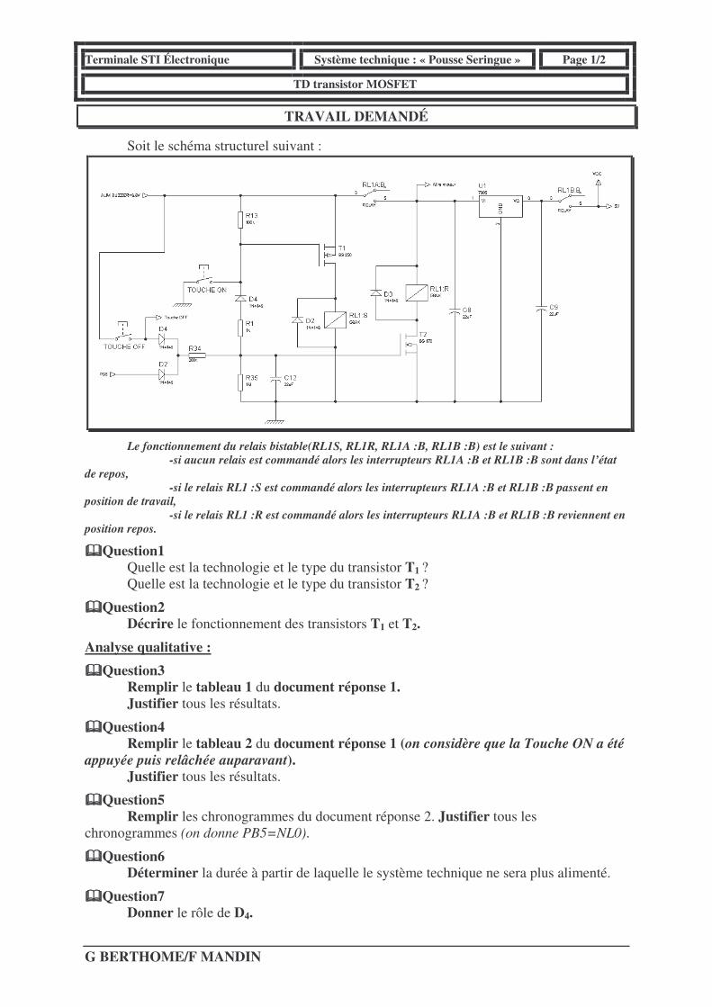
Soit le schéma structurel suivant :
Le fonctionnement du relais bistable(RL1S, RL1R, RL1A :B, RL1B :B) est le suivant : -si aucun relais est commandé alors les interrupteurs RL1A :B et RL1B :B sont dans l’état de repos, -si le relais RL1 :S est commandé alors les interrupteurs RL1A :B et RL1B :B passent en position de travail, -si le relais RL1 :R est commandé alors les interrupteurs RL1A :B et RL1B :B reviennent en position repos.
Question1 Quelle est la technologie et le type du transistor T1 ? Quelle est la technologie et le type du transistor T2 ?
Question2 Décrire le fonctionnement des transistors T1 et T2.
Analyse qualitative :
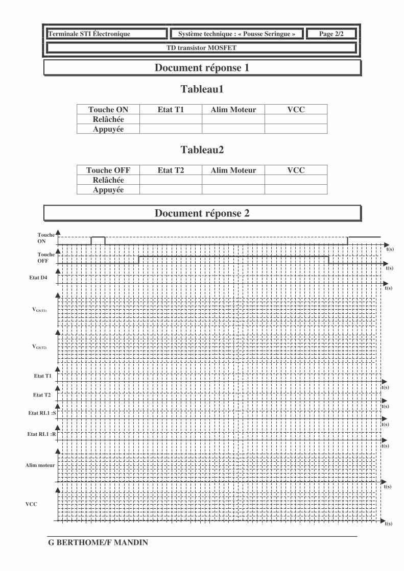
Question3 Remplir le tableau 1 du document réponse 1. Justifier tous les résultats.
Question4 Remplir le tableau 2 du document réponse 1 (on considère que la Touche ON a été
appuyée puis relâchée auparavant). Justifier tous les résultats.
Question5 Remplir les chronogrammes du document réponse 2. Justifier tous les chronogrammes (on donne PB5=NL0).
Question6 Déterminer la durée à partir de laquelle le système technique ne sera plus alimenté.
Question7 Donner le rôle de D4.
Terminale STI Électronique Système technique : « Pousse Seringue » Page 2/2
TD transistor MOSFET
G BERTHOME/F MANDIN
Document réponse 1
Tableau1
Touche ON Etat T1 Alim Moteur VCC Relâchée Appuyée
Tableau2
Touche OFF Etat T2 Alim Moteur VCC
Relâchée Appuyée
Document réponse 2
t(s)
t(s)
t(s)
Touche ON
Touche OFF
Etat D4
t(s)
Etat T1
t(s)
Etat T2
t(s)
Etat RL1 :S
t(s)
Etat RL1 :R
VGS(T1)
VGS(T2)
Alim moteur
VCC
t(s)
t(s)
Semiconductor Components Industries, LLC, 2000
November, 2000 – Rev. 21 Publication Order Number:
BS170/D
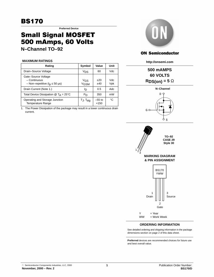
BS170Preferred Device
Small Signal MOSFET500 mAmps, 60 VoltsN–Channel TO–92
MAXIMUM RATINGS
Rating Symbol Value Unit
Drain–Source Voltage VDS 60 Vdc
Gate–Source Voltage– Continuous– Non–repetitive (tp ≤ 50 µs)
VGSVGSM
±20±40
VdcVpk
Drain Current (Note 1.) ID 0.5 Adc
Total Device Dissipation @ TA = 25°C PD 350 mW
Operating and Storage JunctionTemperature Range
TJ, Tstg –55 to+150
°C
1. The Power Dissipation of the package may result in a lower continuous draincurrent.
ORDERING INFORMATION
See detailed ordering and shipping information in the packagedimensions section on page 2 of this data sheet.
BS170
Y = YearWW = Work Week
YWW
http://onsemi.com
MARKING DIAGRAM& PIN ASSIGNMENT
D
G
TO–92CASE 29Style 30
N–Channel
S
1 23
1Drain
3Source
2Gate
500 mAMPS60 VOLTS
RDS(on) = 5 Ω
Preferred devices are recommended choices for future useand best overall value.
BS170
http://onsemi.com2
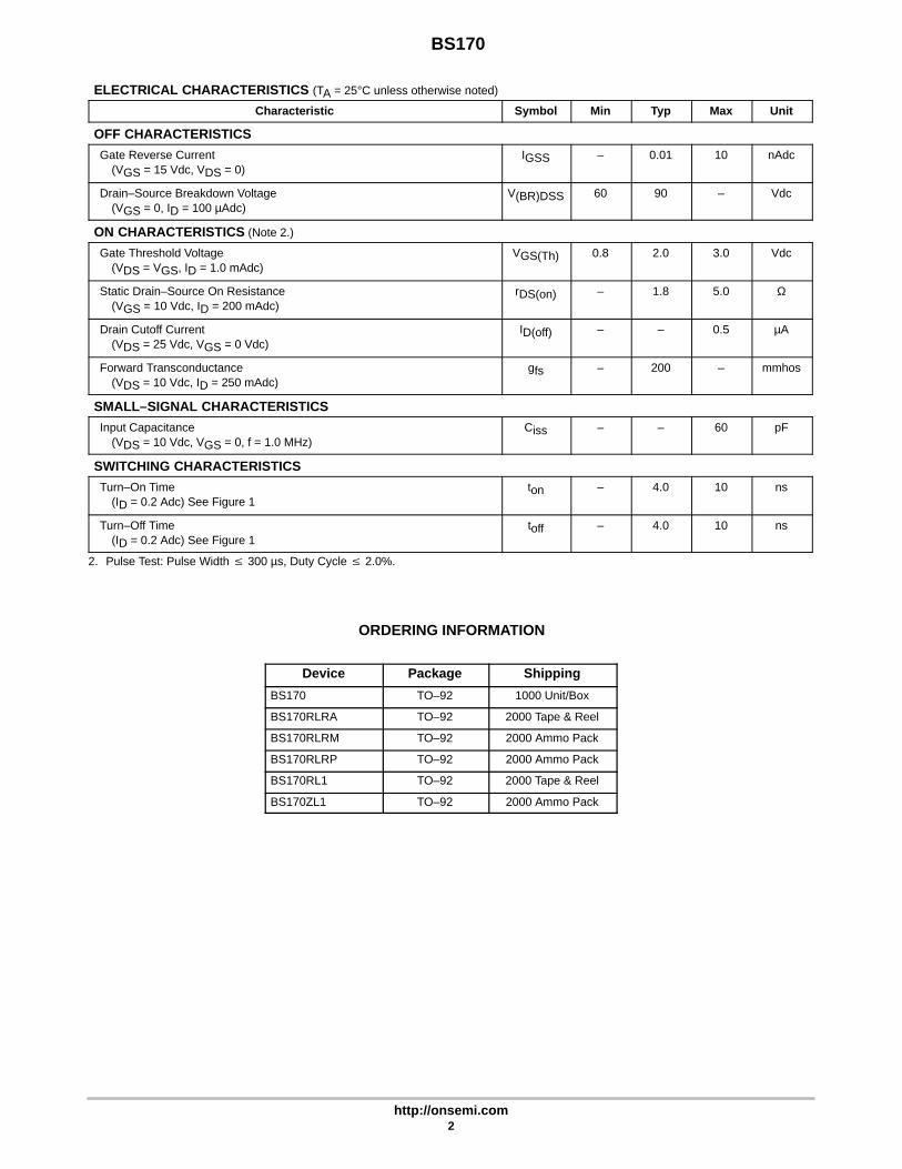
ELECTRICAL CHARACTERISTICS (TA = 25°C unless otherwise noted)
Characteristic Symbol Min Typ Max Unit
OFF CHARACTERISTICS
Gate Reverse Current(VGS = 15 Vdc, VDS = 0)
IGSS – 0.01 10 nAdc
Drain–Source Breakdown Voltage(VGS = 0, ID = 100 µAdc)
V(BR)DSS 60 90 – Vdc
ON CHARACTERISTICS (Note 2.)
Gate Threshold Voltage(VDS = VGS, ID = 1.0 mAdc)
VGS(Th) 0.8 2.0 3.0 Vdc
Static Drain–Source On Resistance(VGS = 10 Vdc, ID = 200 mAdc)
rDS(on) – 1.8 5.0 Ω
Drain Cutoff Current(VDS = 25 Vdc, VGS = 0 Vdc)
ID(off) – – 0.5 µA
Forward Transconductance(VDS = 10 Vdc, ID = 250 mAdc)
gfs – 200 – mmhos
SMALL–SIGNAL CHARACTERISTICS
Input Capacitance(VDS = 10 Vdc, VGS = 0, f = 1.0 MHz)
Ciss – – 60 pF
SWITCHING CHARACTERISTICS
Turn–On Time(ID = 0.2 Adc) See Figure 1
ton – 4.0 10 ns
Turn–Off Time(ID = 0.2 Adc) See Figure 1
toff – 4.0 10 ns
2. Pulse Test: Pulse Width 300 µs, Duty Cycle 2.0%.
ORDERING INFORMATION
Device Package Shipping
BS170 TO–92 1000 Unit/Box
BS170RLRA TO–92 2000 Tape & Reel
BS170RLRM TO–92 2000 Ammo Pack
BS170RLRP TO–92 2000 Ammo Pack
BS170RL1 TO–92 2000 Tape & Reel
BS170ZL1 TO–92 2000 Ammo Pack
BS170
http://onsemi.com3
, DR
AIN
CU
RR
EN
T (A
MP
S)
D(o
n)I
, DR
AIN
CU
RR
EN
T (A
MP
S)
D(o
n)I
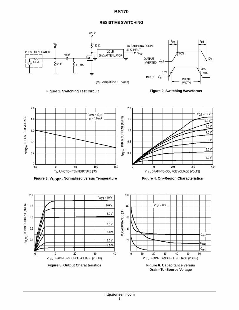
Figure 1. Switching Test Circuit
20 dB
50 Ω ATTENUATORPULSE GENERATOR
+25 V
Vin
40 pF
1.0 MΩ50 Ω
125 Ω
50 Ω
Vout
TO SAMPLING SCOPE
50 Ω INPUT
OUTPUT
INVERTED
INPUTPULSEWIDTH
10%
50%10%
90%
90%
toffton
Figure 2. Switching Waveforms
RESISTIVE SWITCHING
(Vin Amplitude 10 Volts)
Vin
Vout
2.0
1.6
1.2
0.8
0.4
0
, TH
RE
SH
OLD
VO
LTA
GE
50 1500 50 100
TJ, JUNCTION TEMPERATURE (°C)
VG
S(t
h)
VDS, DRAIN-TO-SOURCE VOLTAGE (VOLTS)
0.8
0.4
1.2
2.0
1.6
1.0 2.0 3.0 4.00
VDS, DRAIN-TO-SOURCE VOLTAGE (VOLTS)
0.8
0.4
1.2
1.6
2.0
0 10 20 30
VDS, DRAIN-TO-SOURCE VOLTAGE (VOLTS)
C, C
AP
AC
ITA
NC
E (
pF)
0 10 20 30 40 50
60
40
20
80
100
40 60
Figure 3. V GS(th) Normalized versus Temperature Figure 4. On–Region Characteristics
Figure 5. Output Characteristics Figure 6. Capacitance versusDrain–To–Source Voltage
VGS = 10 V
VGS = 0 V
Ciss
Coss
Crss
9.0 V
8.0 V
7.0 V
6.0 V
5.0 V
4.0 V
VDS = VGSID = 1.0 mA
VGS = 10 V
9.0 V
8.0 V
7.0 V
6.0 V
5.0 V
4.0 V
BS170
http://onsemi.com4
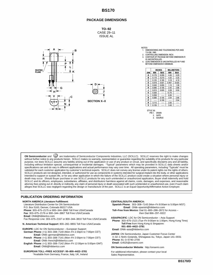
PACKAGE DIMENSIONS
STYLE 30:PIN 1. DRAIN
2. GATE3. SOURCE
NOTES:1. DIMENSIONING AND TOLERANCING PER ANSI
Y14.5M, 1982.2. CONTROLLING DIMENSION: INCH.3. CONTOUR OF PACKAGE BEYOND DIMENSION R
IS UNCONTROLLED.4. LEAD DIMENSION IS UNCONTROLLED IN P AND
BEYOND DIMENSION K MINIMUM.
R
A
P
J
L
B
K
GH
SECTION X–X
CV
D
N
N
X X
SEATING
PLANE DIM MIN MAX MIN MAX
MILLIMETERSINCHES
A 0.175 0.205 4.45 5.20
B 0.170 0.210 4.32 5.33
C 0.125 0.165 3.18 4.19
D 0.016 0.021 0.407 0.533
G 0.045 0.055 1.15 1.39
H 0.095 0.105 2.42 2.66
J 0.015 0.020 0.39 0.50
K 0.500 --- 12.70 ---
L 0.250 --- 6.35 ---
N 0.080 0.105 2.04 2.66
P --- 0.100 --- 2.54
R 0.115 --- 2.93 ---
V 0.135 --- 3.43 ---1
TO–92CASE 29–11
ISSUE AL
ON Semiconductor and are trademarks of Semiconductor Components Industries, LLC (SCILLC). SCILLC reserves the right to make changeswithout further notice to any products herein. SCILLC makes no warranty, representation or guarantee regarding the suitability of its products for any particularpurpose, nor does SCILLC assume any liability arising out of the application or use of any product or circuit, and specifically disclaims any and all liability,including without limitation special, consequential or incidental damages. “Typical” parameters which may be provided in SCILLC data sheets and/orspecifications can and do vary in different applications and actual performance may vary over time. All operating parameters, including “Typicals” must bevalidated for each customer application by customer’s technical experts. SCILLC does not convey any license under its patent rights nor the rights of others.SCILLC products are not designed, intended, or authorized for use as components in systems intended for surgical implant into the body, or other applicationsintended to support or sustain life, or for any other application in which the failure of the SCILLC product could create a situation where personal injury ordeath may occur. Should Buyer purchase or use SCILLC products for any such unintended or unauthorized application, Buyer shall indemnify and holdSCILLC and its officers, employees, subsidiaries, affiliates, and distributors harmless against all claims, costs, damages, and expenses, and reasonableattorney fees arising out of, directly or indirectly, any claim of personal injury or death associated with such unintended or unauthorized use, even if such claimalleges that SCILLC was negligent regarding the design or manufacture of the part. SCILLC is an Equal Opportunity/Affirmative Action Employer.
PUBLICATION ORDERING INFORMATIONCENTRAL/SOUTH AMERICA:Spanish Phone : 303–308–7143 (Mon–Fri 8:00am to 5:00pm MST)
Email : ONlit–[email protected]–Free from Mexico: Dial 01–800–288–2872 for Access –
then Dial 866–297–9322
ASIA/PACIFIC : LDC for ON Semiconductor – Asia SupportPhone : 303–675–2121 (Tue–Fri 9:00am to 1:00pm, Hong Kong Time)
Toll Free from Hong Kong & Singapore:001–800–4422–3781
Email : ONlit–[email protected]
JAPAN : ON Semiconductor, Japan Customer Focus Center4–32–1 Nishi–Gotanda, Shinagawa–ku, Tokyo, Japan 141–0031Phone : 81–3–5740–2700Email : [email protected]
ON Semiconductor Website : http://onsemi.com
For additional information, please contact your localSales Representative.
BS170/D
NORTH AMERICA Literature Fulfillment :Literature Distribution Center for ON SemiconductorP.O. Box 5163, Denver, Colorado 80217 USAPhone : 303–675–2175 or 800–344–3860 Toll Free USA/CanadaFax: 303–675–2176 or 800–344–3867 Toll Free USA/CanadaEmail : [email protected] Response Line: 303–675–2167 or 800–344–3810 Toll Free USA/Canada
N. American Technical Support : 800–282–9855 Toll Free USA/Canada
EUROPE: LDC for ON Semiconductor – European SupportGerman Phone : (+1) 303–308–7140 (Mon–Fri 2:30pm to 7:00pm CET)
Email : ONlit–[email protected] Phone : (+1) 303–308–7141 (Mon–Fri 2:00pm to 7:00pm CET)
Email : ONlit–[email protected] Phone : (+1) 303–308–7142 (Mon–Fri 12:00pm to 5:00pm GMT)
Email : [email protected]
EUROPEAN TOLL–FREE ACCESS*: 00–800–4422–3781*Available from Germany, France, Italy, UK, Ireland
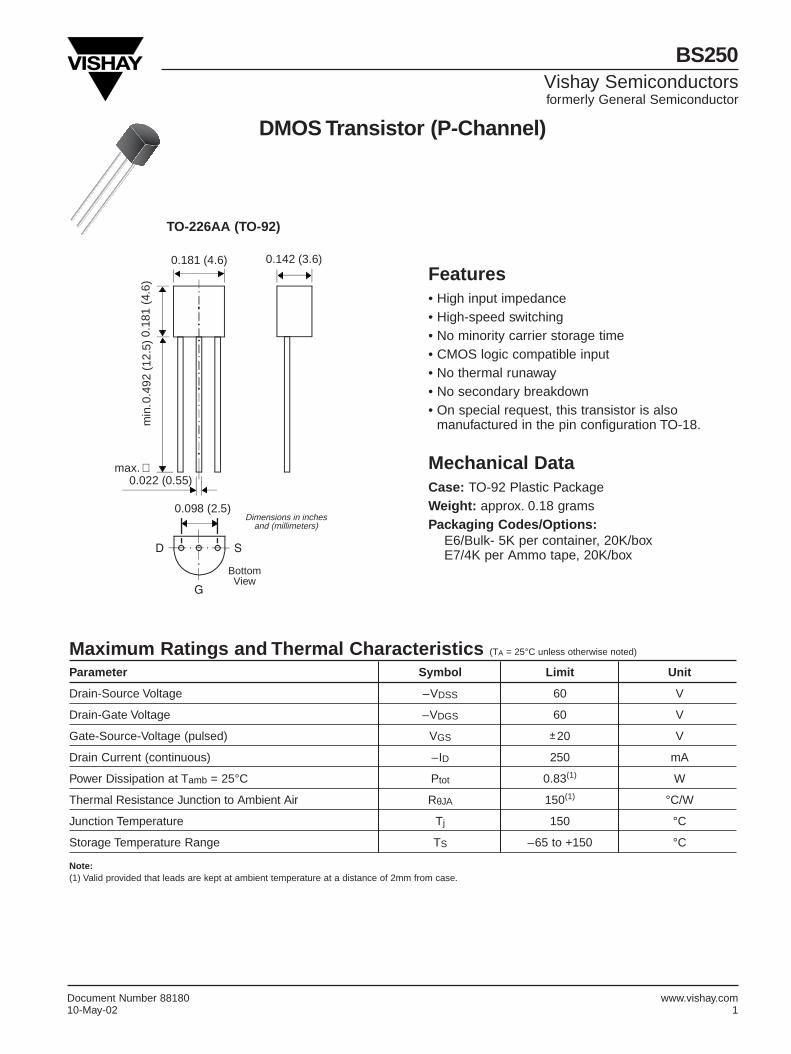
BS250Vishay Semiconductorsformerly General Semiconductor
Document Number 88180 www.vishay.com10-May-02 1
DMOS Transistor (P-Channel)
Maximum Ratings and Thermal Characteristics (TA = 25°C unless otherwise noted)
Parameter Symbol Limit Unit
Drain-Source Voltage –VDSS 60 V
Drain-Gate Voltage –VDGS 60 V
Gate-Source-Voltage (pulsed) VGS ±20 V
Drain Current (continuous) –ID 250 mA
Power Dissipation at Tamb = 25°C Ptot 0.83(1) W
Thermal Resistance Junction to Ambient Air RθJA 150(1) °C/W
Junction Temperature Tj 150 °C
Storage Temperature Range TS –65 to +150 °C
Note:(1) Valid provided that leads are kept at ambient temperature at a distance of 2mm from case.
Features• High input impedance• High-speed switching• No minority carrier storage time• CMOS logic compatible input• No thermal runaway• No secondary breakdown• On special request, this transistor is also
manufactured in the pin configuration TO-18.
Mechanical DataCase: TO-92 Plastic PackageWeight: approx. 0.18 gramsPackaging Codes/Options:
E6/Bulk- 5K per container, 20K/boxE7/4K per Ammo tape, 20K/box
TO-226AA (TO-92)
0.181 (4.6)
min
. 0.4
92 (
12.5
)0.
181
(4.6
)
0.142 (3.6)
0.098 (2.5)
max. ∅ 0.022 (0.55)
Bottom View
Dimensions in inchesand (millimeters)
BS250Vishay Semiconductorsformerly General Semiconductor
www.vishay.com Document Number 881802 10-May-02
Electrical Characteristics (TJ = 25°C unless otherwise noted)
Parameter Symbol Test Condition Min Typ Max Unit
Drain-Source Breakdown Voltage –V(BR)DSS –ID = 100µA, VGS = 0 60 70 — V
Gate-Source Threshold Voltage –VGS(th) VGS = VDS, –ID = 1mA 1.0 2.0 3.0 V
Gate-Body Leakage Current –IGSS –VGS = 15V, VDS = 0 — — 20 nA
Drain Cutoff Current –IDSS –VDS = 25V, VGS = 0 — — 0.5 µA
Drain-Source ON Resistance RDS(on) –VGS = 10V, –ID = 0.2A — 3.5 5.0 Ω
Forward Transconductance gm–VDS = 10V, –ID = 0.2A
— 150 — mSf = 1MHz
Input Capacitance Ciss–VDS = 10V, VGS = 0, — 60 — pF
f = 1MHz
Turn-On Time ton –VGS = 10V, –VDS = 10V — 5 — ns
Turn-Off Time toff RD = 100Ω — 25 — ns
Inverse DiodeParameters Symbol Test Condition Value Unit
Maximum Forward Current (continuous) IF Tamb = 25°C 0.3 A
Forward Voltage Drop (typ.) VFVGS = 0, IF = 0.12A
0.85 VTj = 25°C
BS250Vishay Semiconductorsformerly General Semiconductor
Document Number 88180 www.vishay.com10-May-02 3
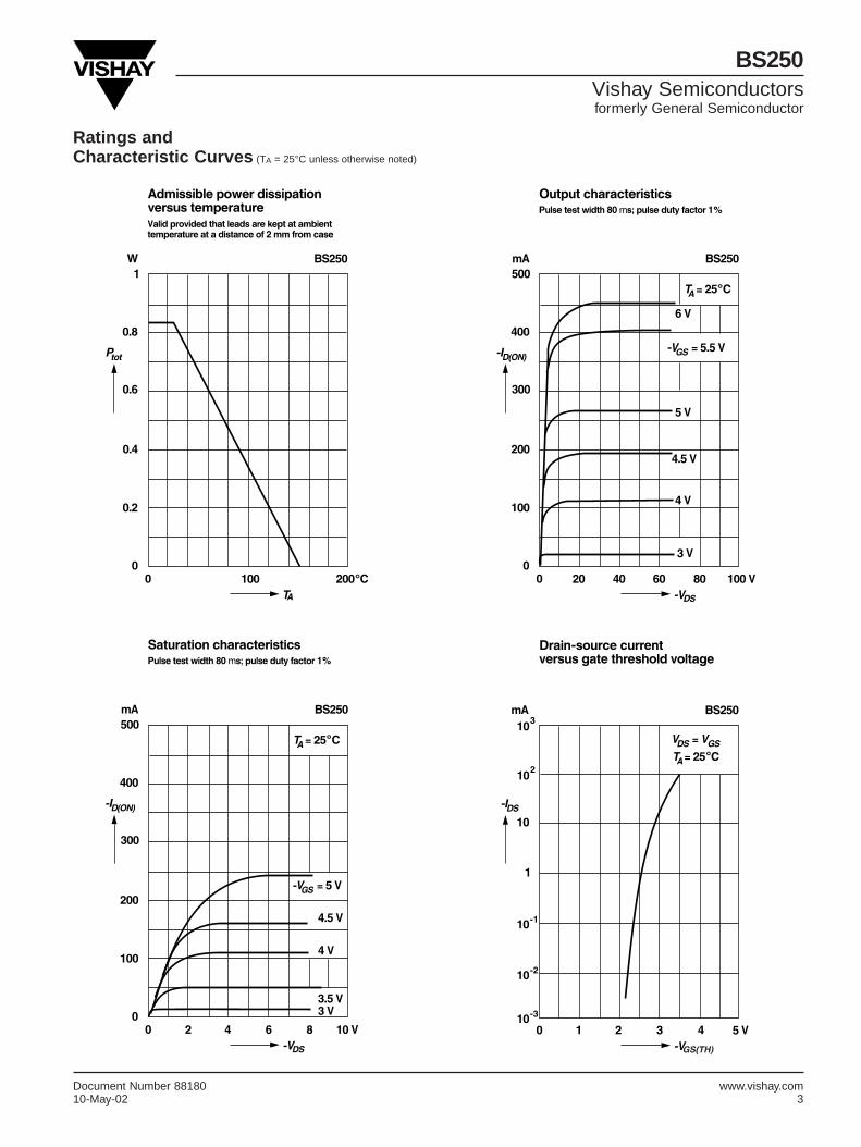
Ratings and Characteristic Curves (TA = 25°C unless otherwise noted)
BS250Vishay Semiconductorsformerly General Semiconductor
www.vishay.com Document Number 881804 10-May-02
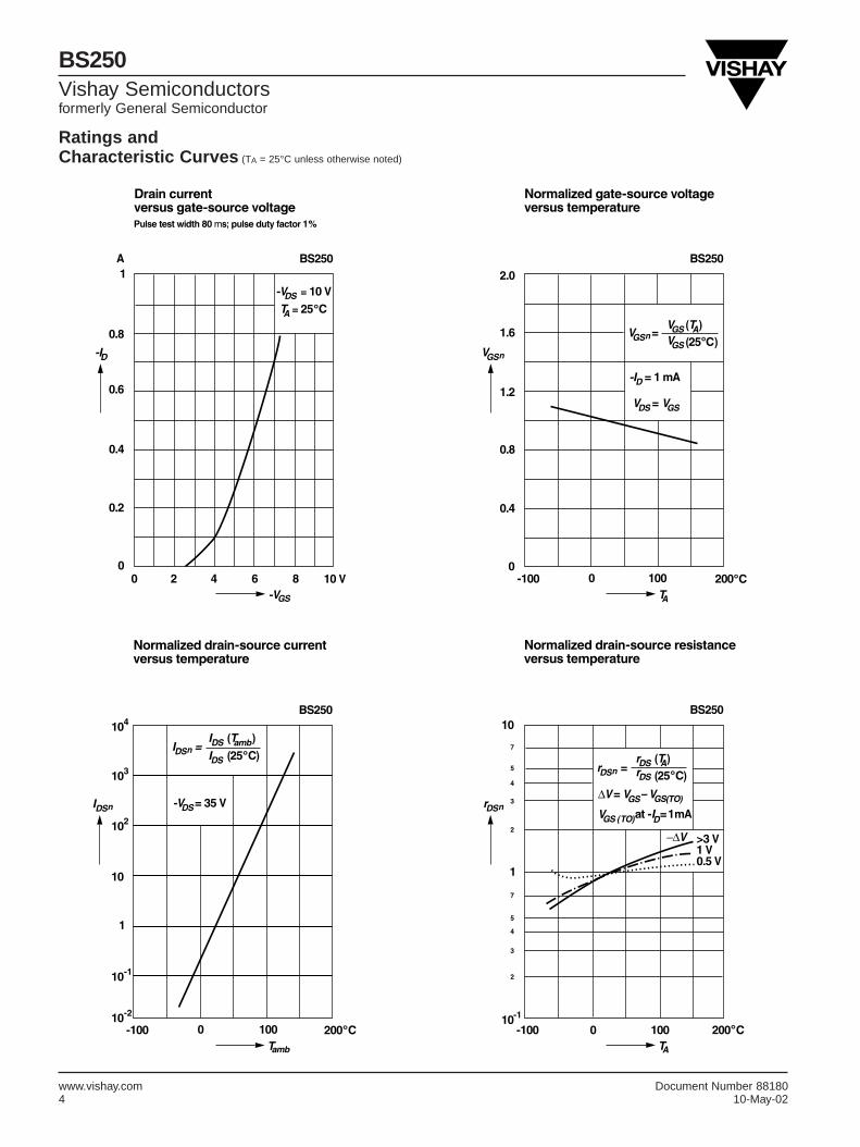
Ratings and Characteristic Curves (TA = 25°C unless otherwise noted)
BS250Vishay Semiconductorsformerly General Semiconductor
Document Number 88180 www.vishay.com10-May-02 5
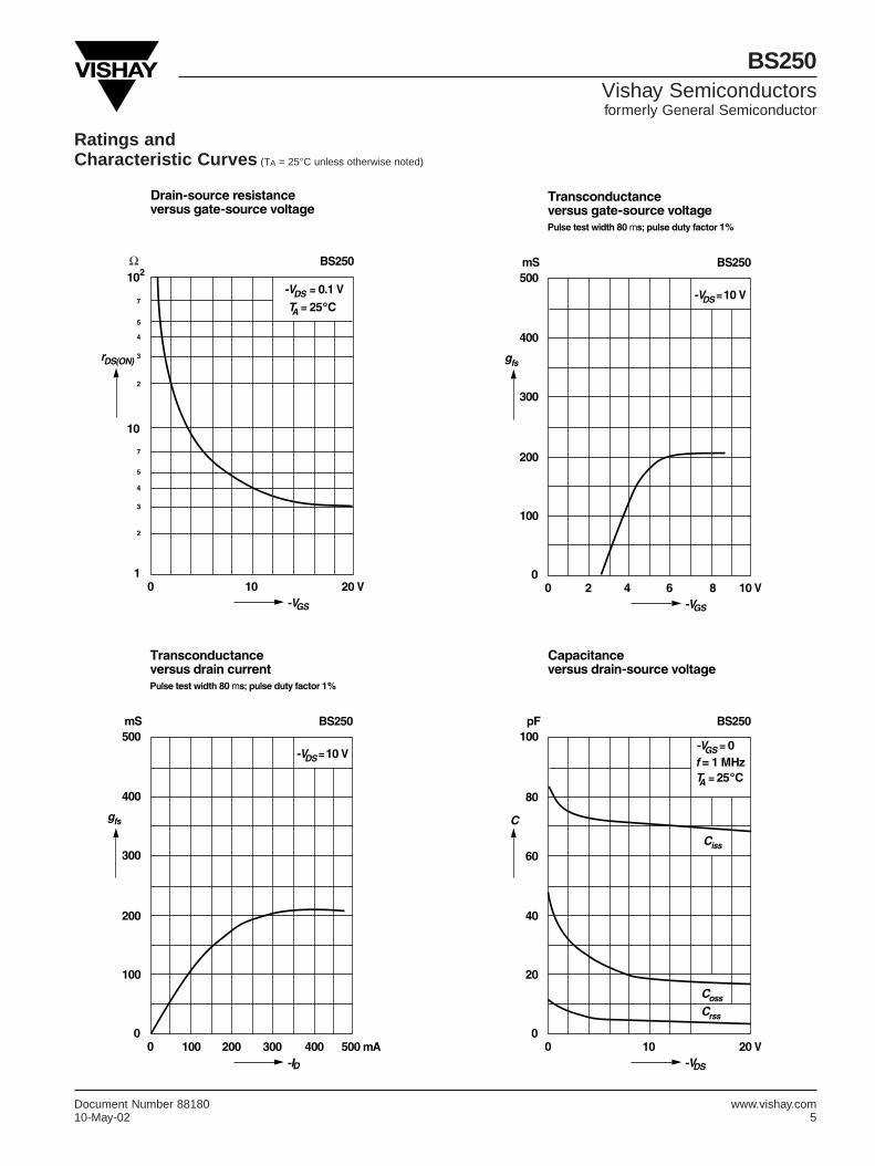
Ratings and Characteristic Curves (TA = 25°C unless otherwise noted)
High sensitivity – can be driven by digitalcircuits
Low-profile design allows use in 12.70 mm(0.50 in) PC board rack
Surge withstand voltage meets FCC Part 68regulation
Units can be mounted side by side due tolow magnetic leakage
Special models available for ultrasoniccleaning and low thermoelectromotive force
Unique moving loop (permanent magnet)armature reduces relay size, magneticinterference, and contact bounce time
Single or double coil winding types available
Low Signal Relay G6A
Ordering Information
Part number
Type Contact form AgPd (Au clad) Ag (Au clad)
Standard DPDT G6A-234P-ST-US G6A-274P-ST-US
4PDT G6A-434P-ST-US G6A-474P-ST-US
High-sensitivity DPDT G6A-234P-ST15-US G6A-274P-ST15-US
4PDT G6A-434P-ST20-US G6A-474P-ST20-US
Low-sensitivity DPDT G6A-234P-ST40-US G6A-274P-ST40-US
4PDT G6A-434P-ST40-US G6A-474P-ST40-US
To Order: Select the part number and add the desired coil voltage rating, (e.g., G6A-274P-ST-US-DC12).
NON-LATCHING
Part number
Type Contact form AgPd (Au clad) Ag (Au clad)
Standard DPDT G6AU-234P-ST-US G6AU-274P-ST-US
4PDT G6AU-434P-ST-US G6AU-474P-ST-US
LATCHING
Single coil
Part number
Type Contact form AgPd (Au clad) Ag (Au clad)
Standard DPDT G6AK-234P-ST-US G6AK-274P-ST-US
4PDT G6AK-434P-ST-US G6AK-474P-ST-US
Low-sensitivity DPDT G6AK-234P-ST40-US G6AK-274P-ST40-US
4PDT G6AK-434P-ST40-US G6AK-474P-ST40-US
Dual coil
Note: Other options available for ST10 ultra high reliability, high temperature 85°C (185°F), ST1 reverse coil polarity, BS Britishstandard. Contact your OMRON sales representative for details.
2
G6A G6A
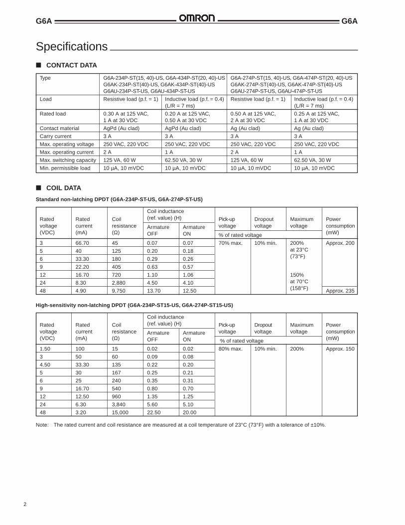
Specifications CONTACT DATA
Type G6A-234P-ST(15, 40)-US, G6A-434P-ST(20, 40)-US G6A-274P-ST(15, 40)-US, G6A-474P-ST(20, 40)-USG6AK-234P-ST(40)-US, G6AK-434P-ST(40)-US G6AK-274P-ST(40)-US, G6AK-474P-ST(40)-USG6AU-234P-ST-US, G6AU-434P-ST-US G6AU-274P-ST-US, G6AU-474P-ST-US
Load Resistive load (p.f. = 1) Inductive load (p.f. = 0.4) Resistive load (p.f. = 1) Inductive load (p.f. = 0.4)(L/R = 7 ms) (L/R = 7 ms)
Rated load 0.30 A at 125 VAC, 0.20 A at 125 VAC, 0.50 A at 125 VAC, 0.25 A at 125 VAC,1 A at 30 VDC 0.50 A at 30 VDC 2 A at 30 VDC 1 A at 30 VDC
Contact material AgPd (Au clad) AgPd (Au clad) Ag (Au clad) Ag (Au clad)
Carry current 3 A 3 A 3 A 3 A
Max. operating voltage 250 VAC, 220 VDC 250 VAC, 220 VDC 250 VAC, 220 VDC 250 VAC, 220 VDC
Max. operating current 2 A 1 A 2 A 1 A
Max. switching capacity 125 VA, 60 W 62.50 VA, 30 W 125 VA, 60 W 62.50 VA, 30 W
Min. permissible load 10 µA, 10 mVDC 10 µA, 10 mVDC 10 µA, 10 mVDC 10 µA, 10 mVDC
Note: The rated current and coil resistance are measured at a coil temperature of 23°C (73°F) with a tolerance of ±10%.
COIL DATA
Standard non-latching DPDT (G6A-234P-ST-US, G6A-274P-ST-US)
Coil inductance
Rated Rated Coil (ref. value) (H) Pick-up Dropout Maximum Powervoltage current resistance Armature Armature voltage voltage voltage consumption(VDC) (mA) (Ω) OFF ON % of rated voltage (mW)
3 66.70 45 0.07 0.07 70% max. 10% min. 200% Approx. 200
5 40 125 0.20 0.18 at 23°C
6 33.30 180 0.29 0.26 (73°F)
9 22.20 405 0.63 0.57
12 16.70 720 1.10 1.06 150%
24 8.30 2,880 4.50 4.10 at 70°C
48 4.90 9,750 13.70 12.50 (158°F) Approx. 235
High-sensitivity non-latching DPDT (G6A-234P-ST15-US, G6A-274P-ST15-US)
Coil inductance
Rated Rated Coil (ref. value) (H) Pick-up Dropout Maximum Powervoltage current resistance Armature Armature voltage voltage voltage consumption(VDC) (mA) (Ω) OFF ON % of rated voltage (mW)
1.50 100 15 0.02 0.02 80% max. 10% min. 200% Approx. 150
3 50 60 0.09 0.08
4.50 33.30 135 0.22 0.20
5 30 167 0.25 0.21
6 25 240 0.35 0.31
9 16.70 540 0.80 0.70
12 12.50 960 1.35 1.25
24 6.30 3,840 5.60 5.10
48 3.20 15,000 22.50 20.00
3
G6A G6A
Note: The rated current and coil resistance are measured at a coil temperature of 23°C (73°F) with a tolerance of ±10%.
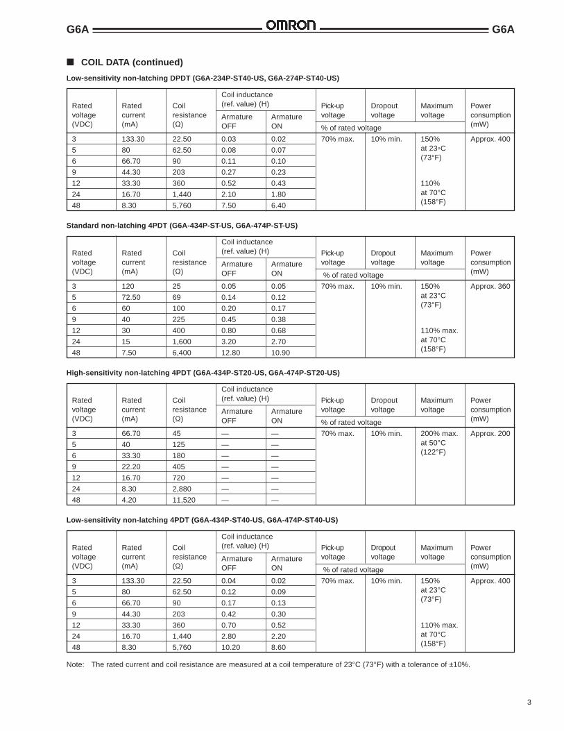
COIL DATA (continued)
Low-sensitivity non-latching DPDT (G6A-234P-ST40-US, G6A-274P-ST40-US)
Coil inductance
Rated Rated Coil (ref. value) (H) Pick-up Dropout Maximum Powervoltage current resistance Armature Armature voltage voltage voltage consumption(VDC) (mA) (Ω) OFF ON % of rated voltage (mW)
3 133.30 22.50 0.03 0.02 70% max. 10% min. 150% Approx. 400
5 80 62.50 0.08 0.07 at 23°C
6 66.70 90 0.11 0.10 (73°F)
9 44.30 203 0.27 0.23
12 33.30 360 0.52 0.43 110%
24 16.70 1,440 2.10 1.80 at 70°C
48 8.30 5,760 7.50 6.40 (158°F)
Standard non-latching 4PDT (G6A-434P-ST-US, G6A-474P-ST-US)
Coil inductance
Rated Rated Coil (ref. value) (H) Pick-up Dropout Maximum Powervoltage current resistance Armature Armature voltage voltage voltage consumption(VDC) (mA) (Ω) OFF ON % of rated voltage (mW)
3 120 25 0.05 0.05 70% max. 10% min. 150% Approx. 360
5 72.50 69 0.14 0.12 at 23°C
6 60 100 0.20 0.17 (73°F)
9 40 225 0.45 0.38
12 30 400 0.80 0.68 110% max.
24 15 1,600 3.20 2.70 at 70°C
48 7.50 6,400 12.80 10.90 (158°F)
High-sensitivity non-latching 4PDT (G6A-434P-ST20-US, G6A-474P-ST20-US)
Coil inductance
Rated Rated Coil (ref. value) (H) Pick-up Dropout Maximum Powervoltage current resistance Armature Armature voltage voltage voltage consumption(VDC) (mA) (Ω) OFF ON % of rated voltage (mW)
3 66.70 45 — — 70% max. 10% min. 200% max. Approx. 200
5 40 125 — — at 50°C
6 33.30 180 — — (122°F)
9 22.20 405 — —
12 16.70 720 — —
24 8.30 2,880 — —
48 4.20 11,520 — —
Low-sensitivity non-latching 4PDT (G6A-434P-ST40-US, G6A-474P-ST40-US)
Coil inductance
Rated Rated Coil (ref. value) (H) Pick-up Dropout Maximum Powervoltage current resistance Armature Armature voltage voltage voltage consumption(VDC) (mA) (Ω) OFF ON % of rated voltage (mW)
3 133.30 22.50 0.04 0.02 70% max. 10% min. 150% Approx. 400
5 80 62.50 0.12 0.09 at 23°C
6 66.70 90 0.17 0.13 (73°F)
9 44.30 203 0.42 0.30
12 33.30 360 0.70 0.52 110% max.
24 16.70 1,440 2.80 2.20 at 70°C
48 8.30 5,760 10.20 8.60 (158°F)
4
G6A G6A
Note: The rated current and coil resistance are measured at a coil temperature of 23°C (73°F) with a tolerance of ±10%.
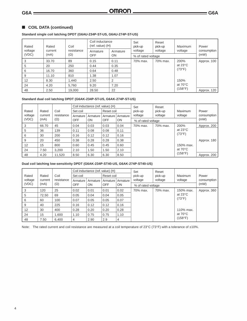
COIL DATA (continued)
Standard single coil latching DPDT (G6AU-234P-ST-US, G6AU-274P-ST-US)
Coil inductance Set ResetRated Rated Coil (ref. value) (H) pick-up pick-up Maximum Powervoltage current resistance Armature Armature voltage voltage voltage consumption(VDC) (mA) (Ω) OFF ON % of rated voltage (mW)
3 33.70 89 0.15 0.11 70% max. 70% max. 200% Approx. 100
5 20 250 0.44 0.35 at 23°C
6 16.70 360 0.64 0.48 (73°F)
9 11.10 810 1.38 1.07
12 8.30 1,440 2.50 2 150%
24 4.20 5,760 9.20 7.20 at 70°C
48 2.50 19,000 28.50 22 (158°F) Approx. 120
Standard dual coil latching DPDT (G6AK-234P-ST-US, G6AK-274P-ST-US)
Coil inductance (ref. value) (H) Set ResetRated Rated Coil Set coil Reset coil pick-up pick-up Maximum Powervoltage current resistance Armature Armature Armature Armature voltage voltage voltage consumption(VDC) (mA) (Ω) OFF ON OFF ON % of rated voltage (mW)
3 66.70 45 0.04 0.03 0.03 0.04 70% max. 70% max. 200% Approx. 200
5 36 139 0.11 0.08 0.08 0.11 at 23°C
6 30 200 0.16 0.12 0.12 0.16 (73°F)
9 20 450 0.38 0.28 0.28 0.38 Approx. 180
12 15 800 0.60 0.45 0.45 0.60 150% max.
24 7.50 3,200 2.10 1.50 1.50 2.10 at 70°C
48 4.20 11,520 8.50 6.30 6.30 8.50 (158°F) Approx. 200
Dual coil latching low-sensitivity DPDT (G6AK-234P-ST40-US, G6AK-274P-ST40-US)
Coil inductance (ref. value) (H) Set ResetRated Rated Coil Set coil Reset coil pick-up pick-up Maximum Powervoltage current resistance Armature Armature Armature Armature voltage voltage voltage consumption(VDC) (mA) (Ω) OFF ON OFF ON % of rated voltage (mW)
3 120 25 0.02 0.01 0.01 0.02 70% max. 70% max. 150% max. Approx. 360
5 72.50 69 0.05 0.04 0.04 0.05 at 23°C
6 60 100 0.07 0.05 0.05 0.07 (73°F)
9 40 225 0.16 0.12 0.12 0.16
12 30 400 0.28 0.20 0.20 0.28 110% max.
24 15 1,600 1.10 0.75 0.75 1.10 at 70°C
48 7.50 6,400 4 2.90 2.9 4 (158°F)
5
G6A G6A
Note: The rated current and coil resistance are measured at a coil temperature of 23°C (73°F) with a tolerance of ±10%.
COIL DATA (continued)
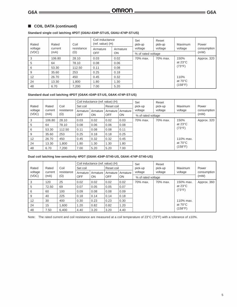
Standard single coil latching 4PDT (G6AU-434P-ST-US, G6AU-474P-ST-US)
Coil inductance Set ResetRated Rated Coil (ref. value) (H) pick-up pick-up Maximum Powervoltage current resistance Armature Armature voltage voltage voltage consumption(VDC) (mA) (Ω) OFF ON % of rated voltage (mW)
3 106.80 28.10 0.03 0.02 70% max. 70% max. 150% Approx. 320
5 64 78.10 0.08 0.06 at 23°C
6 53.30 112.50 0.11 0.08 (73°F)
9 35.60 253 0.25 0.18
12 26.70 450 0.45 0.32 110%
24 13.30 1,800 1.80 1.30 at 70°C
48 6.70 7,200 7.00 5.20 (158°F)
Standard dual coil latching 4PDT (G6AK-434P-ST-US, G6AK-474P-ST-US)
Coil inductance (ref. value) (H) Set ResetRated Rated Coil Set coil Reset coil pick-up pick-up Maximum Powervoltage current resistance Armature Armature Armature Armature voltage voltage voltage consumption(VDC) (mA) (Ω) OFF ON OFF ON % of rated voltage (mW)
3 106.80 28.10 0.03 0.02 0.02 0.03 70% max. 70% max. 150% Approx. 320
5 64 78.10 0.08 0.06 0.06 0.08 at 23°C
6 53.30 112.50 0.11 0.08 0.08 0.11 (73°F)
9 35.60 253 0.25 0.18 0.18 0.25
12 26.70 450 0.45 0.32 0.32 0.45 110% max.
24 13.30 1,800 1.80 1.30 1.30 1.80 at 70°C
48 6.70 7,200 7.00 5.20 5.20 7.00 (158°F)
Dual coil latching low-sensitivity 4PDT (G6AK-434P-ST40-US, G6AK-474P-ST40-US)
Coil inductance (ref. value) (H) Set ResetRated Rated Coil Set coil Reset coil pick-up pick-up Maximum Powervoltage current resistance Armature Armature Armature Armature voltage voltage voltage consumption(VDC) (mA) (Ω) OFF ON OFF ON % of rated voltage (mW)
3 120 25 0.02 0.02 0.02 0.02 70% max. 70% max. 150% max. Approx. 360
5 72.50 69 0.07 0.05 0.05 0.07 at 23°C
6 60 100 0.09 0.08 0.08 0.09 (73°F)
9 40 225 0.18 0.14 0.14 0.18
12 30 400 0.30 0.23 0.23 0.30 110% max.
24 15 1,600 1.20 0.82 0.82 1.20 at 70°C
48 7.50 6,400 4.40 3.20 3.20 4.40 (158°F)
6
G6A G6A
Type Non-latching Latching
Contact resistance 50 mΩ max.
Operate (set) time DPDT 5 ms max. (mean value: approx. 3 ms) 5 ms max. (mean value: approx. 2.50 ms)
4PDT 7 ms max. (mean value: approx. 3.80 ms) 7 ms max. (mean value: approx. 3.30 ms)
Release (reset) time DPDT 3 ms max. (mean value: approx. 1.20 ms) 5 ms max. (mean value: approx. 2.50 ms)
4PDT 5 ms max. (mean value: approx. 1.30 ms) 7 ms max. (mean value: approx. 2.70 ms)
Bounce time Operate Actual value approx. 0.50 ms
Release Actual value approx. 0.50 ms
Operating Mechanical 36,000 operations/hourfrequency Electrical 1,800 operations/hour (under rated load)
Insulation resistance 1,000 MΩ min. (at 500 VDC)
Dielectric strength (see note 2) 1,000 VAC, 50/60 Hz for 1 minute between coil and contacts
1,000 VAC, 50/60 Hz for 1 minute between contacts of different poles
1,000 VAC, 50/60 Hz for 1 minute between contacts of same pole
250 VAC, 50/60 Hz for 1 minute between set and reset coils
Surge withstand voltage (see note 3) 1,500 V 10 x 160 µs (conforms to FCC Part 68)
Vibration Mechanical durability 10 to 55 Hz; 5 mm (0.20 in) double amplitude
Malfunction durability 10 to 55 Hz; 3.30 mm (0.13 in) double amplitude
Shock Mechanical durability 1,000 m/s2 (Approx. 100 G)
Malfunction durability DPDT: 500 m/s2 (Approx. 50 G); 4PDT: 300 m/s2 (Approx. 30 G)
Ambient temperature -40° to 70°C (-40° to 158°F)
Humidity 45% to 85% RH
Service life (see note 4) Mechanical 100 million operations min. (at 36,000 operations/hour)
Electrical See “Characteristic Data”
Weight DPDT Approx. 3.5 g (0.12 oz)
4PDT Approx 6.0 g (0.21 oz)
Note: 1. Data shown are of initial value.2. The dielectric strength of Type G6A-2D34P-ST-US is 500 VAC when the relay is not energized.3. The surge withstand of Type G6A-2D34P-ST-US is 1,000 V 10 x 160 µs when the relay is not energized.4. The mechanical service life of Type G6A-2D34P-ST-US is 10,000,000 operations min.
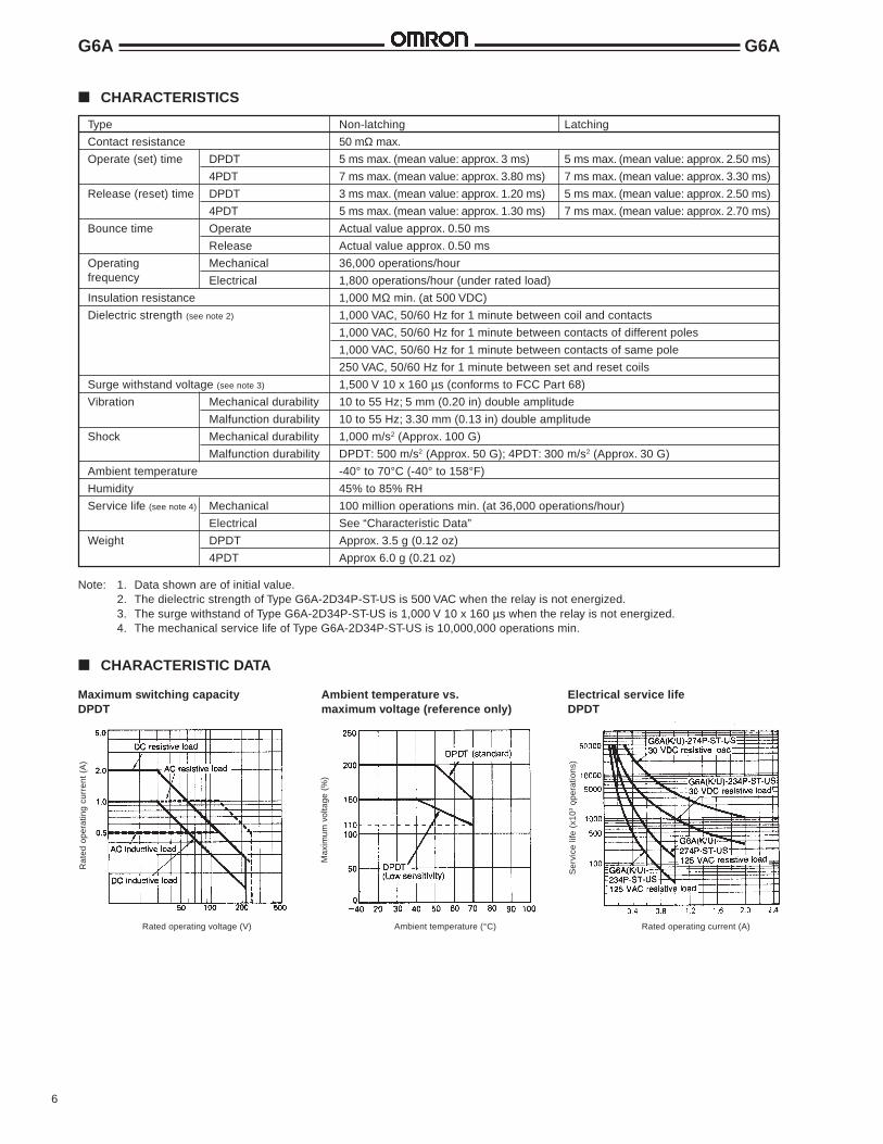
CHARACTERISTICS
CHARACTERISTIC DATA
Maximum switching capacityDPDT
Ambient temperature vs.maximum voltage (reference only)
Max
imum
vol
tage
(%
)
Ambient temperature (°C)
Rat
ed o
pera
ting
curr
ent
(A)
Rated operating voltage (V)
Electrical service lifeDPDT
Ser
vice
life
(x1
03 o
pera
tions
)
Rated operating current (A)
7
G6A G6A
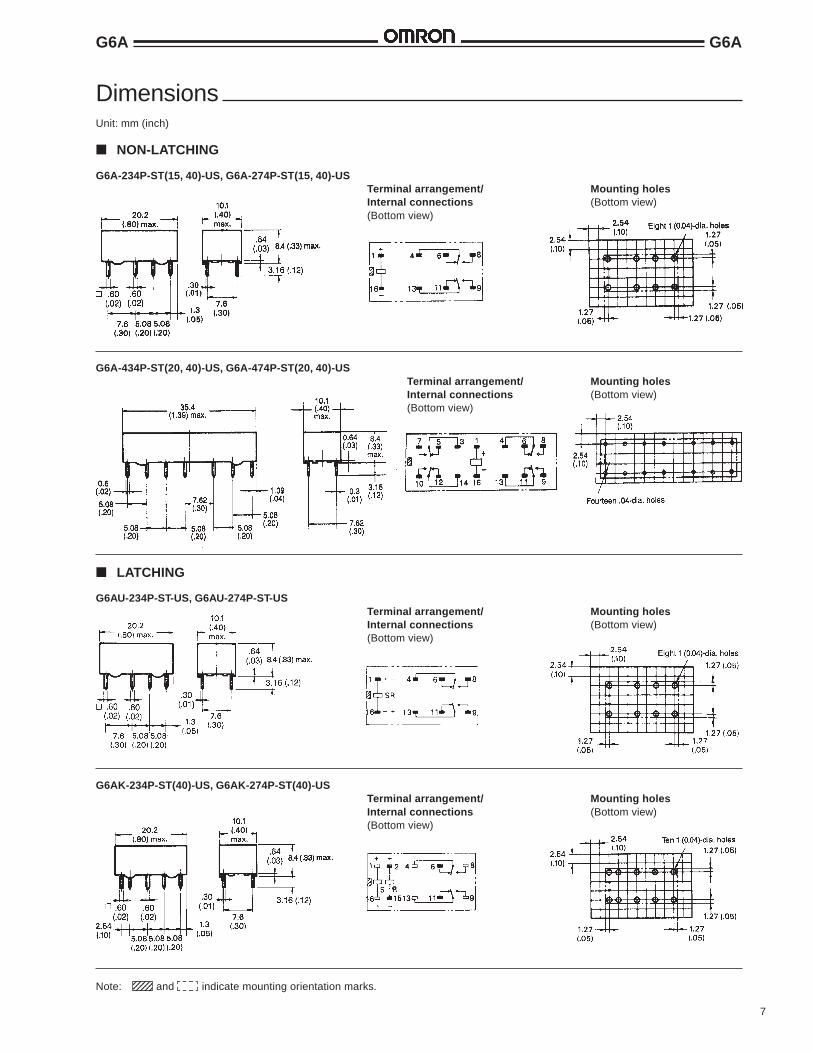
DimensionsUnit: mm (inch)
G6A-234P-ST(15, 40)-US, G6A-274P-ST(15, 40)-USTerminal arrangement/ Mounting holesInternal connections (Bottom view)(Bottom view)
NON-LATCHING
G6AU-234P-ST-US, G6AU-274P-ST-USTerminal arrangement/ Mounting holesInternal connections (Bottom view)(Bottom view)
LATCHING
G6AK-234P-ST(40)-US, G6AK-274P-ST(40)-USTerminal arrangement/ Mounting holesInternal connections (Bottom view)(Bottom view)
Note: and indicate mounting orientation marks.123456123456123456
G6A-434P-ST(20, 40)-US, G6A-474P-ST(20, 40)-USTerminal arrangement/ Mounting holesInternal connections (Bottom view)(Bottom view)
8
G6A G6A
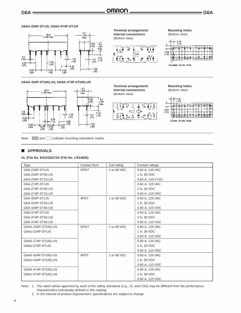
G6AU-434P-ST-US, G6AU-474P-ST-USTerminal arrangement/ Mounting holesInternal connections (Bottom view)(Bottom view)
G6AK-434P-ST(40)-US, G6AK-474P-ST(40)-USTerminal arrangement/ Mounting holesInternal connections (Bottom view)(Bottom view)
Note: and indicate mounting orientation marks.123451234512345
Type Contact form Coil rating Contact ratings
G6A-234P-ST-US DPDT 1 to 48 VDC 0.60 A, 125 VAC
G6A-234P-ST40-US 1 A, 30 VDC
G6A-234P-ST15-US 0.60 A, 110 V+DC
G6A-274P-ST-US 0.60 A, 125 VAC
G6A-274P-ST40-US 2 A, 30 VDC
G6A-274P-ST15-US 0.60 A, 110 VDC
G6A-434P-ST-US 4PDT 1 to 48 VDC 0.60 A, 125 VAC
G6A-434P-ST20-US 1 A, 30 VDC
G6A-434P-ST40-US 0.60 A, 110 VDC
G6A-474P-ST-US 0.60 A, 125 VAC
G6A-474P-ST20-US 2 A, 30 VDC
G6A-474P-ST40-US 0.60 A, 110 VDC
G6AK-234P-ST(40)-US DPDT 1 to 48 VDC 0.60 A, 125 VAC
G6AU-234P-ST-US 1 A, 30 VDC
0.60 A, 110 VDC
G6AK-274P-ST(40)-US 0.60 A, 125 VAC
G6AU-274P-ST-US 2 A, 30 VDC
0.60 A, 110 VDC
G6AK-434P-ST(40)-US 4PDT 1 to 48 VDC 0.60 A, 125 VAC
G6AU-434P-ST(40)-US 1 A, 30 VDC
0.60 A, 110 VDC
G6AK-474P-ST(40)-US 0.60 A, 125 VAC
G6AU-474P-ST(40)-US 2 A, 30 VDC
0.60 A, 110 VDC
APPROVALS
UL (File No. E41515)/CSA (File No. LR24825)
Note: 1. The rated values approved by each of the safety standards (e.g., UL and CSA) may be different from the performancecharacteristics individually defined in this catalog.
2. In the interest of product improvement, specifications are subject to change.
9
G6A G6A
OMRON ELECTRONICS, INC. OMRON CANADA, INC.One East Commerce Drive 885 Milner AvenueSchaumburg, IL 60173 Scarborough, Ontario M1B 5V81-800-55-OMRON 416-286-6465
Cat. No. GC RLY6 9/97 Specifications subject to change without notice. Printed in the U.S.A.