Surface Electron Spectroscopies: Principles and Applications
S. Kaciulis, A. Mezzi
CNR - Istituto per lo Studio dei Materiali Nanostrutturati,
Area della Ricerca Roma 1
Area della Ricerca di Roma 1
Via Salaria Km 29,300
C.P. 10 - 00015 Monterotondo Stazione, Roma
Università di “Tor Vergata”, dip. Ingegneria Industriale – 8 giugno 2015
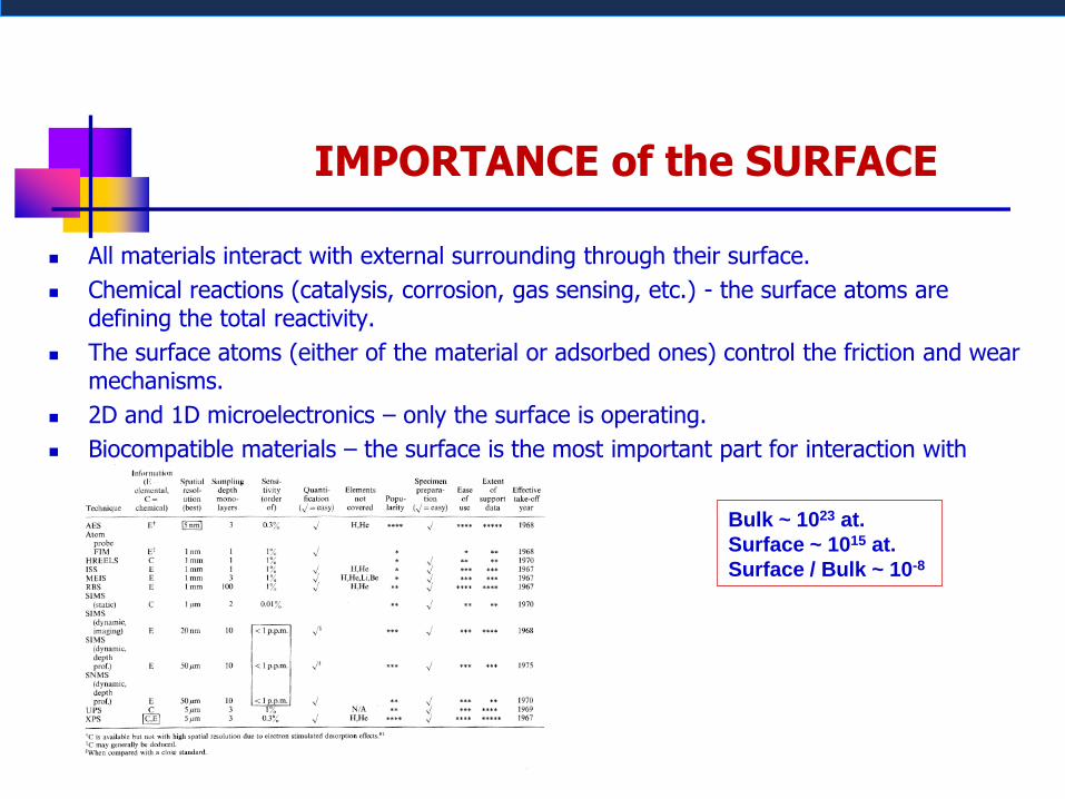
IMPORTANCE of the SURFACE
All materials interact with external surrounding through their surface.
Chemical reactions (catalysis, corrosion, gas sensing, etc.) - the surface atoms are defining the total reactivity.
The surface atoms (either of the material or adsorbed ones) control the friction and wear mechanisms.
2D and 1D microelectronics – only the surface is operating.
Biocompatible materials – the surface is the most important part for interaction with human body.
Bulk ~ 1023 at.
Surface ~ 1015 at.
Surface / Bulk ~ 10-8
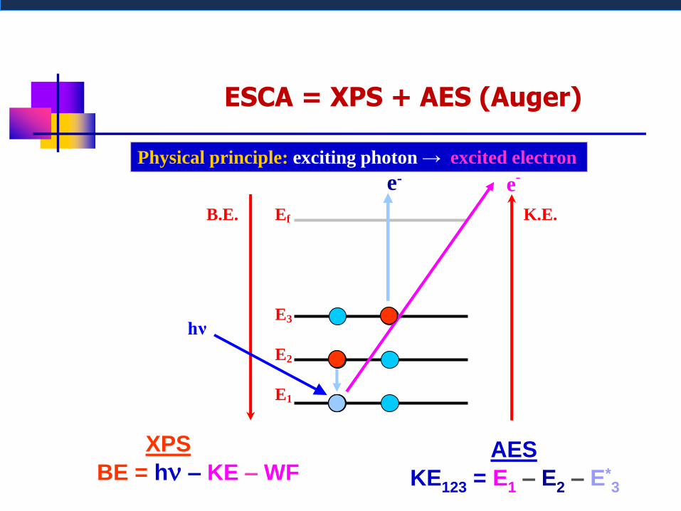
B.E. Ef K.E.
E3
E2
E1
hν
e-
Physical principle: exciting photon → excited electron
BE = hn – KE – WF
e-
AESXPS
KE123 = E1 – E2 – E*3
ESCA = XPS + AES (Auger)
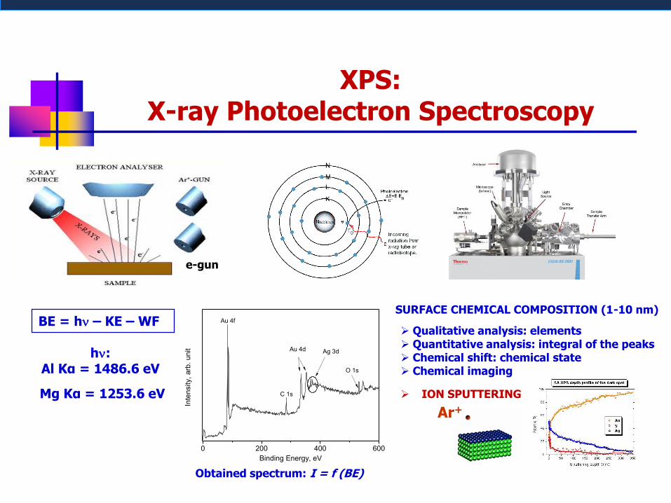
XPS:X-ray Photoelectron Spectroscopy
BE = hn – KE – WF
hn:Al Kα = 1486.6 eV
Mg Kα = 1253.6 eV
Registered signal: I = f (KE)
Obtained spectrum: I = f (BE)
e-gun
0 200 400 600
Inte
nsity,
arb
. u
nit
Binding Energy, eV
Au 4f
C 1s
O 1s
Ag 3dAu 4d
SURFACE CHEMICAL COMPOSITION (1-10 nm)
Qualitative analysis: elements Quantitative analysis: integral of the peaks Chemical shift: chemical state Chemical imaging
Ar+
ION SPUTTERING
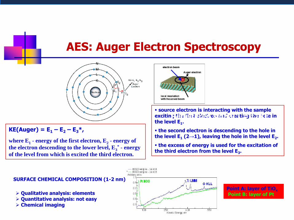
AES: Auger Electron Spectroscopy
KE(Auger) = E1 – E2 – E3*,
where E1 - energy of the first electron, E2 - energy of
the electron descending to the lower level, E3* - energy
of the level from which is excited the third electron.
source electron is interacting with the sample exciting the first electron and creating the hole in the level E1.
the second electron is descending to the hole in the level E1 (2→1), leaving the hole in the level E2.
the excess of energy is used for the excitation of the third electron from the level E3.
Registered signal I = f (KE)
SURFACE CHEMICAL COMPOSITION (1-2 nm)
Qualitative analysis: elements Quantitative analysis: not easy Chemical imaging
Point A: layer of TiOx
Point B: layer of Pt
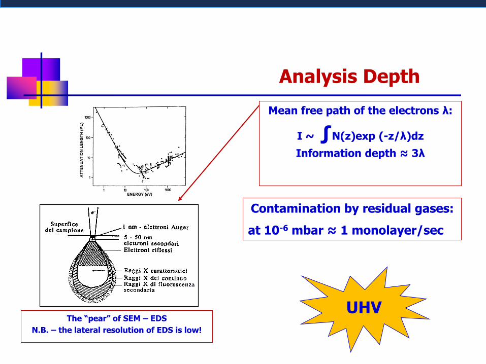
Analysis Depth
The “pear” of SEM – EDS
N.B. – the lateral resolution of EDS is low!
Mean free path of the electrons λ:
I ~ ∫N(z)exp (-z/λ)dz
Information depth ≈ 3λ
Contamination by residual gases:
at 10-6 mbar ≈ 1 monolayer/sec
UHV
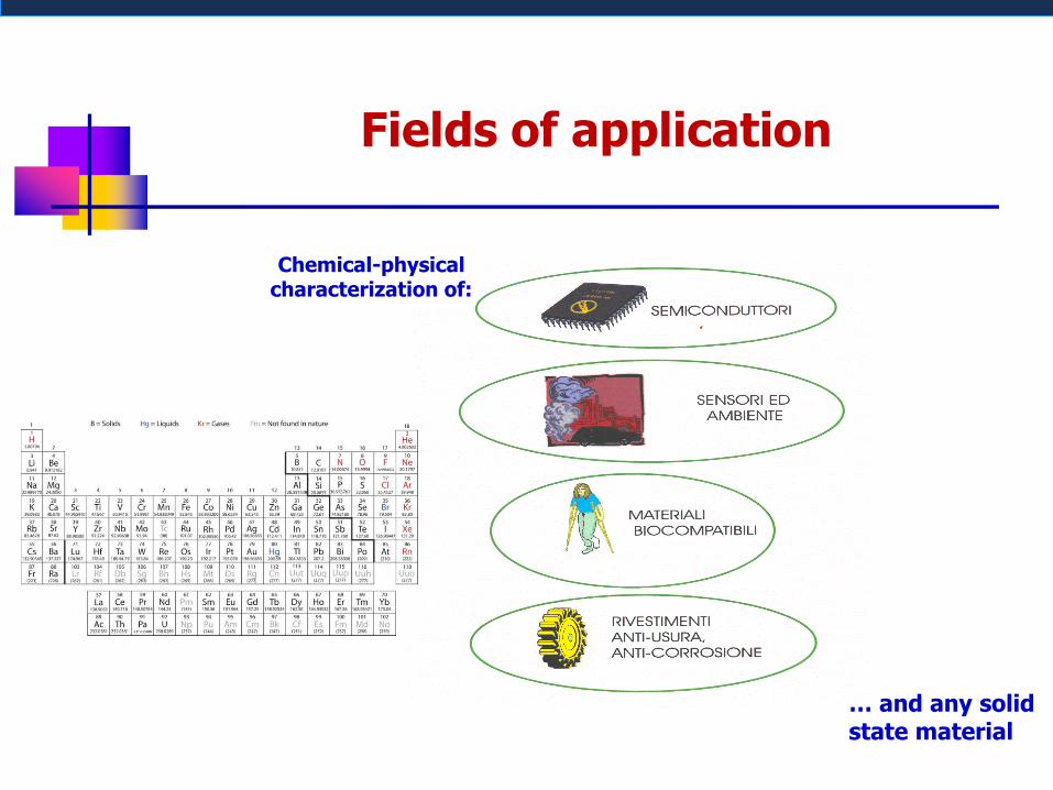
Fields of application
… and any solid state material
Chemical-physicalcharacterization of:
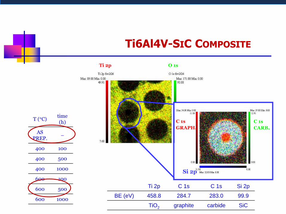
Ti 2p O 1s
C 1s
GRAPH.C 1s
CARB.
Si 2p
Ti 2p C 1s C 1s Si 2p
BE (eV) 458.8 284.7 283.0 99.9
TiO2 graphite carbide SiC
Lateral resolution < 3 μmXPS CHEMICAL IMAGESAxis Ultra spectrometer (Kratos Analytical)
T (°C)time(h)
AS PREP.
–
400 100
400 500
400 1000
600 100
600 500
600 1000
THERMAL TREATMENTS
Ti6Al4V-SIC COMPOSITE
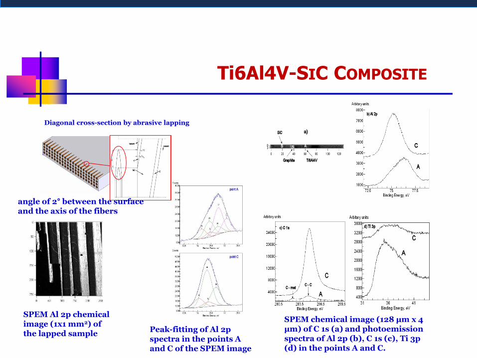
SPEM Al 2p chemical image (1x1 mm2) of the lapped sample
Diagonal cross-section by abrasive lapping
Peak-fitting of Al 2p spectra in the points A and C of the SPEM image
SPEM chemical image (128 μm x 4 μm) of C 1s (a) and photoemission spectra of Al 2p (b), C 1s (c), Ti 3p (d) in the points A and C.
angle of 2° between the surface and the axis of the fibers
Ti6Al4V-SIC COMPOSITE
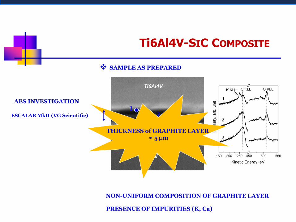
NON-UNIFORM COMPOSITION OF GRAPHITE LAYER
PRESENCE OF IMPURITIES (K, Ca)
SAMPLE AS PREPARED
80 x 80 mm2
Ti6Al4V
Si
12
3THICKNESS of GRAPHITE LAYER
≈ 5 mm
AES INVESTIGATION
ESCALAB MkII (VG Scientific)
Ti6Al4V-SIC COMPOSITE
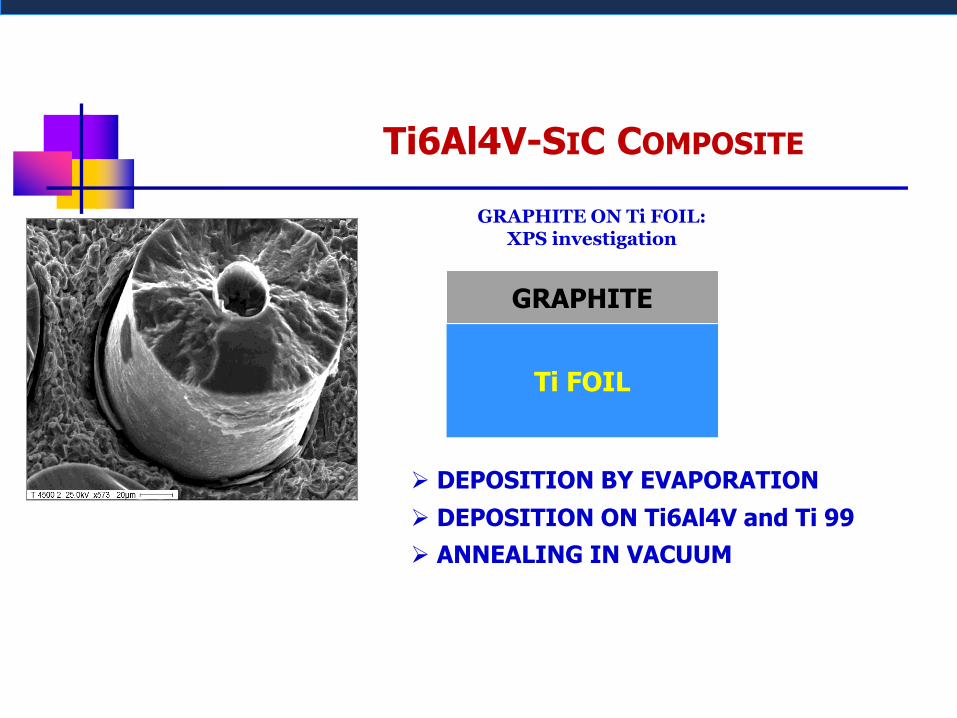
GRAPHITE ON Ti FOIL:XPS investigation
Ti FOIL
GRAPHITE
DEPOSITION BY EVAPORATION
DEPOSITION ON Ti6Al4V and Ti 99.99+
30
nm
ANNEALING IN VACUUM
Ti6Al4V-SIC COMPOSITE
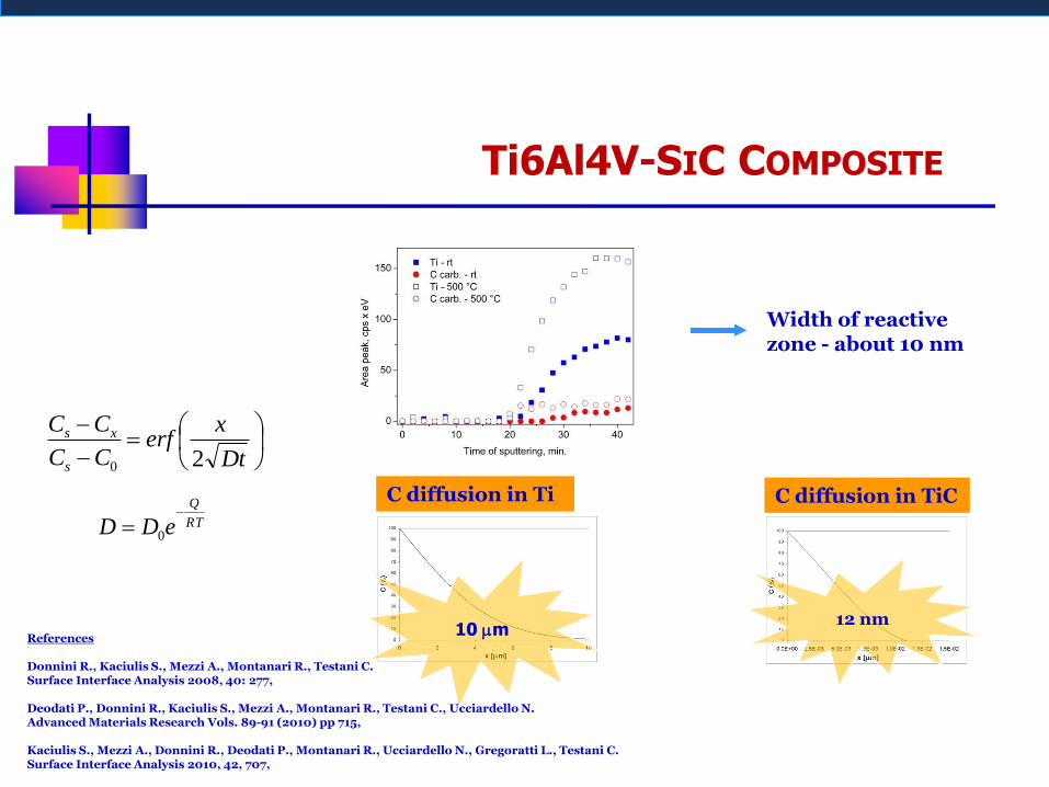
COMPARISON of covered reference samples(RT and 500°C x 8h)
Width of reactivezone - about 10 nm
Dt
xerf
CC
CC
s
xs
20
RT
Q
eDD
0
THEORETICAL APPROACH
C diffusion in Ti C diffusion in TiC
10 mm12 nm
(1)
(2)
Ti6Al4V-SIC COMPOSITE
References
Donnini R., Kaciulis S., Mezzi A., Montanari R., Testani C.Surface Interface Analysis 2008, 40: 277,
Deodati P., Donnini R., Kaciulis S., Mezzi A., Montanari R., Testani C., Ucciardello N.Advanced Materials Research Vols. 89-91 (2010) pp 715,
Kaciulis S., Mezzi A., Donnini R., Deodati P., Montanari R., Ucciardello N., Gregoratti L., Testani C.Surface Interface Analysis 2010, 42, 707,
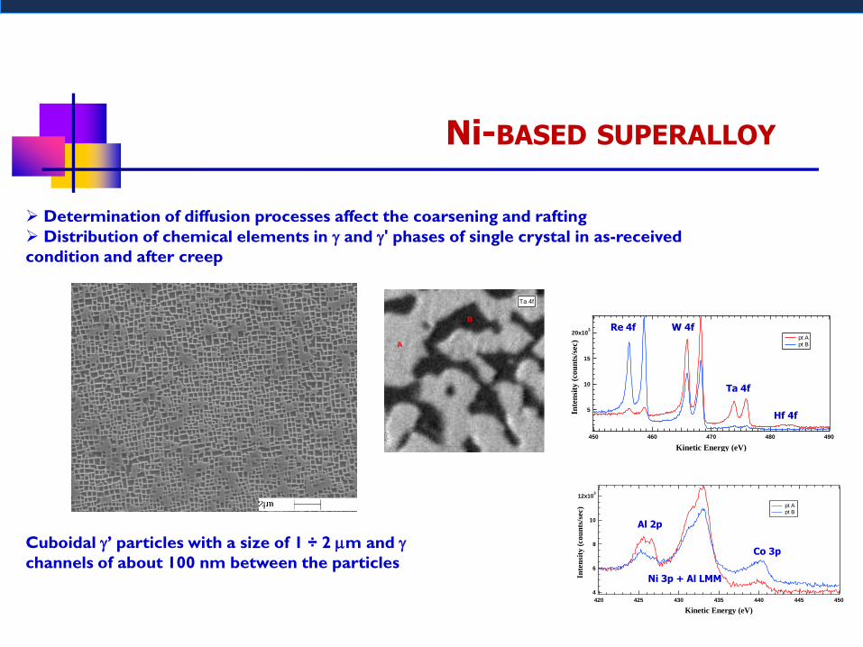
Determination of diffusion processes affect the coarsening and rafting
Distribution of chemical elements in and ' phases of single crystal in as-received
condition and after creep
Cuboidal ’ particles with a size of 1 ÷ 2 mm and
channels of about 100 nm between the particles
Ni-BASED SUPERALLOY
120
100
80
60
40
20
0
120100806040200
A
B
Ta 4f
20x103
15
10
5Inte
nsi
ty (
cou
nts
/sec)
490480470460450
Kinetic Energy (eV)
pt A pt B
12x103
10
8
6
4
Inte
nsi
ty (
cou
nts
/sec)
450445440435430425420
Kinetic Energy (eV)
pt A pt B
Re 4f W 4f
Ta 4f
Hf 4f
Al 2p
Ni 3p + Al LMM
Co 3p
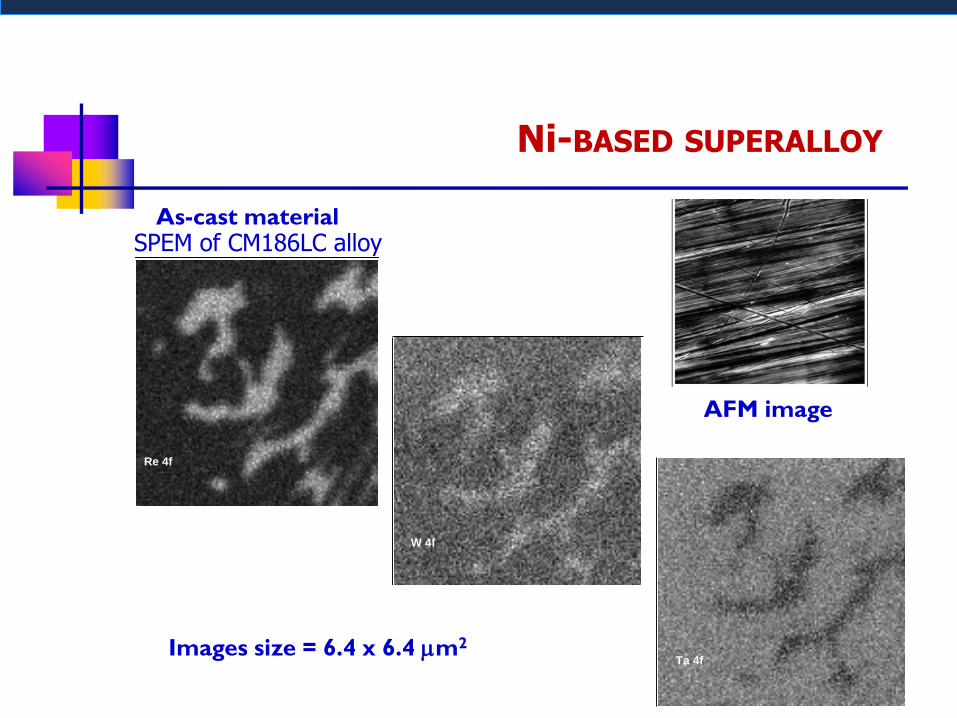
SPEM of CM186LC alloy
120
100
80
60
40
20
0
120100806040200
Re 4f
120
100
80
60
40
20
0
120100806040200
W 4f
120
100
80
60
40
20
0
120100806040200
Ta 4f
As-cast material
AFM image
Images size = 6.4 x 6.4 mm2
Ni-BASED SUPERALLOY
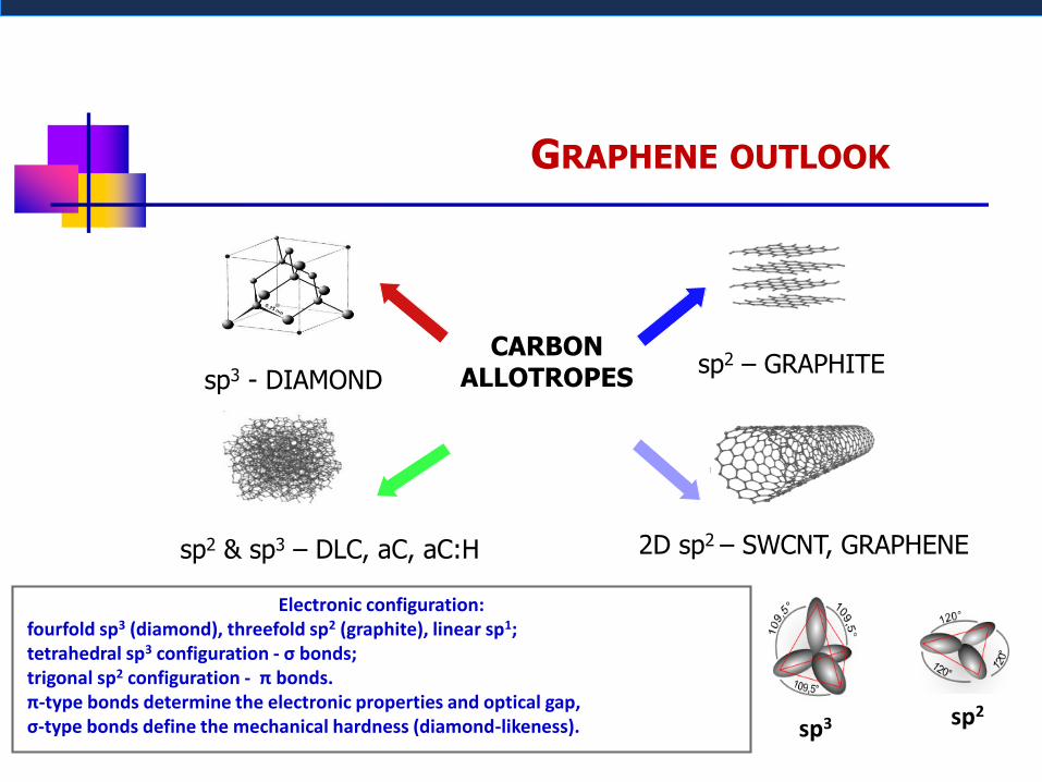
sp3 - DIAMONDsp2 – GRAPHITE
2D sp2 – SWCNT, GRAPHENEsp2 & sp3 – DLC, aC, aC:H
CARBON ALLOTROPES
As-cast material
AFM image
Images size = 6.4 x 6.4 mm2
Electronic configuration:fourfold sp3 (diamond), threefold sp2 (graphite), linear sp1;tetrahedral sp3 configuration - σ bonds;trigonal sp2 configuration - π bonds.π-type bonds determine the electronic properties and optical gap,σ-type bonds define the mechanical hardness (diamond-likeness). sp3 sp2
GRAPHENE OUTLOOK
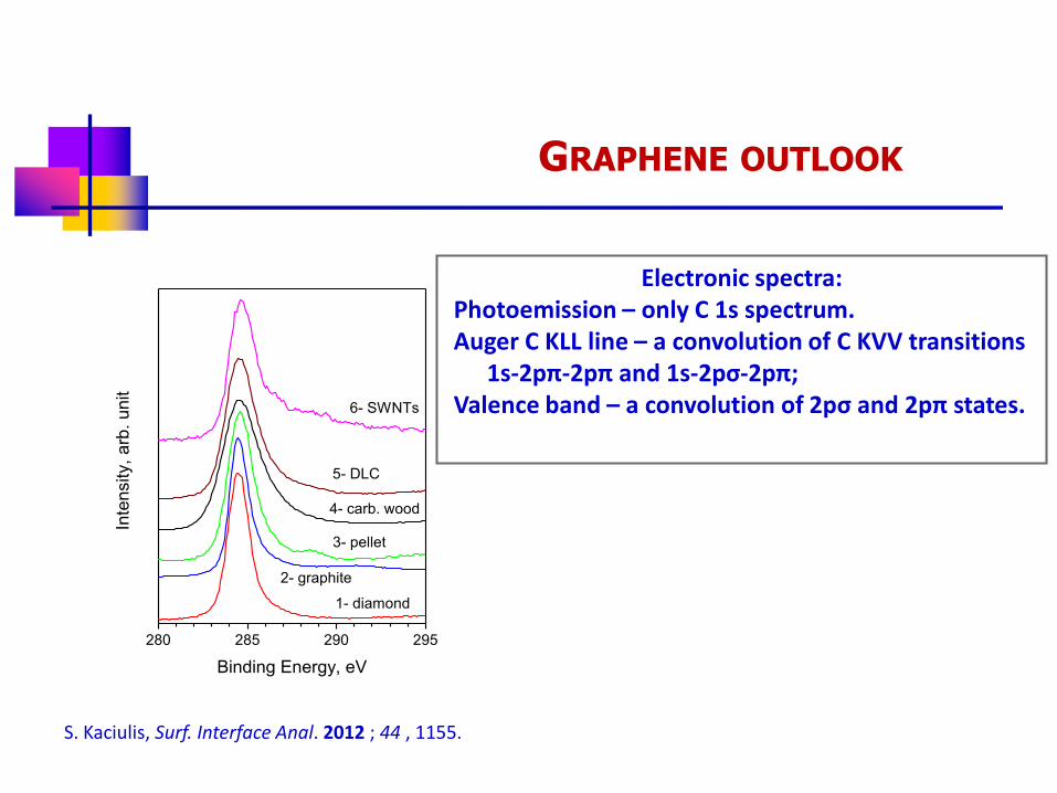
Electronic spectra:Photoemission – only C 1s spectrum.Auger C KLL line – a convolution of C KVV transitions
1s-2pπ-2pπ and 1s-2pσ-2pπ;Valence band – a convolution of 2pσ and 2pπ states.
S. Kaciulis, Surf. Interface Anal. 2012 ; 44 , 1155.
280 285 290 295
2- graphite
1- diamond
6- SWNTs
3- pellet
5- DLC
Inte
nsity,
arb
. u
nit
Binding Energy, eV
4- carb. wood
GRAPHENE OUTLOOK
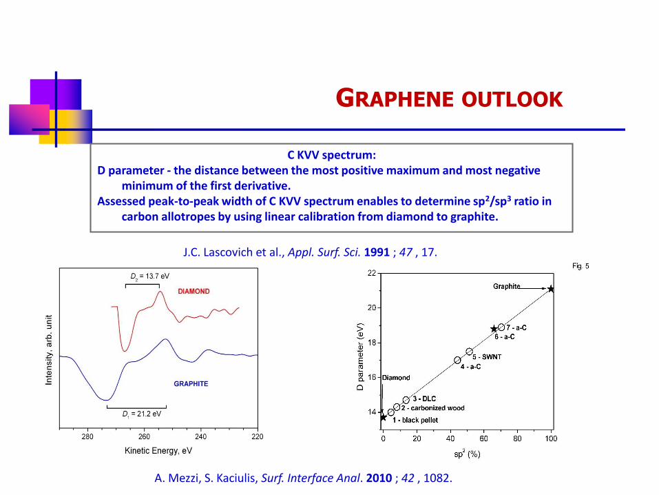
C KVV spectrum:D parameter - the distance between the most positive maximum and most negative
minimum of the first derivative.Assessed peak-to-peak width of C KVV spectrum enables to determine sp2/sp3 ratio in
carbon allotropes by using linear calibration from diamond to graphite.
A. Mezzi, S. Kaciulis, Surf. Interface Anal. 2010 ; 42 , 1082.
J.C. Lascovich et al., Appl. Surf. Sci. 1991 ; 47 , 17.
GRAPHENE OUTLOOK
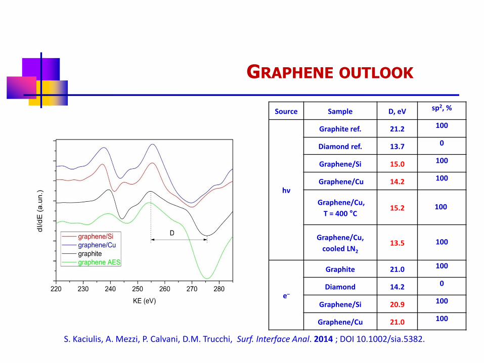
Source Sample D, eV sp2, %
hν
Graphite ref. 21.2 100
Diamond ref. 13.7 0
Graphene/Si 15.0 100
Graphene/Cu 14.2 100
Graphene/Cu,
T = 400 °C15.2 100
Graphene/Cu,
cooled LN2
13.5 100
e–
Graphite 21.0 100
Diamond 14.2 0
Graphene/Si 20.9 100
Graphene/Cu 21.0 100
S. Kaciulis, A. Mezzi, P. Calvani, D.M. Trucchi, Surf. Interface Anal. 2014 ; DOI 10.1002/sia.5382.
GRAPHENE OUTLOOK
GRAPHENE OUTLOOK
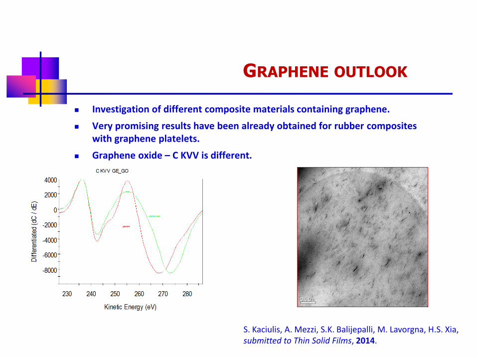
Investigation of different composite materials containing graphene.
Very promising results have been already obtained for rubber compositeswith graphene platelets.
Graphene oxide – C KVV is different.
S. Kaciulis, A. Mezzi, S.K. Balijepalli, M. Lavorgna, H.S. Xia, submitted to Thin Solid Films, 2014.
ACKNOWLEDGMENTS
Università degli Studi di Roma "Tor Vergata"
prof. Montanari R.; prof. Montesperelli, G.; dr. Carbone M.
dr. Lavorgna M.: IMCB (CNR)
dr. Angella G.; IENI (CNR)
dr. Trucchi D.; Suber L.; ISM (CNR)
Bianchi M.; Istituto Ortopedico Rizzoli (Bologna)
dr. Gregoratti L.; ELETTRA Sincrotrone Trieste
prof. Sberveglieri G.; Università degli studi di Brescia
dr. Setkus A.; dr. Bondarenka V.; Semiconductor Physics
Institute (Vilnius)
Wlodarski W.; RMIT University (Melbourne)
Prof. V. Ambrogi, University of Perugia, Italy.
Recommended