Embed Size (px)
Citation preview
Microwave metamaterials made by fused deposition 3D printing of a highly conductivecopper-based filamentYangbo Xie, Shengrong Ye, Christopher Reyes, Pariya Sithikong, Bogdan-Ioan Popa, Benjamin J. Wiley, andSteven A. Cummer
Citation: Appl. Phys. Lett. 110, 181903 (2017); doi: 10.1063/1.4982718View online: http://dx.doi.org/10.1063/1.4982718View Table of Contents: http://aip.scitation.org/toc/apl/110/18Published by the American Institute of Physics
Articles you may be interested inTunable prism based on piezoelectric metamaterial for acoustic beam steeringAppl. Phys. Lett. 110, 181902181902 (2017); 10.1063/1.4982717
Poroelastic metamaterials with negative effective static compressibilityAppl. Phys. Lett. 110, 171901171901 (2017); 10.1063/1.4981783
Fano resonance based ultra high-contrast electromagnetic switchAppl. Phys. Lett. 110, 181904181904 (2017); 10.1063/1.4982725
Electrically tunable and broader-band sound absorption by using micro-perforated dielectric elastomer actuatorAppl. Phys. Lett. 110, 182901182901 (2017); 10.1063/1.4982634
Direct metal writing: Controlling the rheology through microstructureAppl. Phys. Lett. 110, 094104094104 (2017); 10.1063/1.4977555
Micro-silicon phononic crystal with locally resonant theoryAppl. Phys. Lett. 110, 171902171902 (2017); 10.1063/1.4981121
Microwave metamaterials made by fused deposition 3D printing of a highlyconductive copper-based filament
Yangbo Xie,1,a) Shengrong Ye,2,a) Christopher Reyes,2 Pariya Sithikong,1
Bogdan-Ioan Popa,3 Benjamin J. Wiley,2,b) and Steven A. Cummer1,b)
1Department of Electrical and Computer Engineering, Duke University, Durham, North Carolina 27708, USA2Department of Chemistry, Duke University, Durham, North Carolina 27708, USA3Department of Mechanical Engineering, University of Michigan, Ann Arbor, Michigan 48109, USA
(Received 8 February 2017; accepted 18 April 2017; published online 1 May 2017)
This work reports a method for fabricating three-dimensional microwave metamaterials by fused
deposition modeling 3D printing of a highly conductive polymer composite filament. The conduc-
tivity of such a filament is shown to be nearly equivalent to that of a perfect conductor for micro-
wave metamaterial applications. The expanded degrees-of-freedom made available by 3D
metamaterial designs are demonstrated by designing, fabricating, and testing a 3D-printed unit cell
with a broadband permittivity as high as 14.4. The measured and simulated S-parameters agree
well with a mean squared error smaller than 0.1. The presented method not only allows reliable and
convenient fabrication of microwave metamaterials with high conductivity but also opens the door
to exploiting the third dimension of the unit cell design space to achieve enhanced electromagnetic
properties. Published by AIP Publishing. [http://dx.doi.org/10.1063/1.4982718]
Microwave metamaterials are engineered materials
designed to interact with electromagnetic waves1–4 and
exhibit useful effective material properties. Within the
0.3–3 GHz spectral range, such metamaterials are conven-
tionally fabricated on printed circuit boards (PCBs).3,4
Conventional PCB-based fabrication of metamaterials, using
methods such as chemical etching and computer numeric
control (CNC) milling, limits the design space to two-
dimensional planar structures and thus also restricts the
performance of the metamaterials. Moreover, lossy PCB sub-
strates such as FR-4 can cause substantial power absorption
and further reduce metamaterial performance. The handling
of toxic etchants (such as a ferric chloride solution) during
chemical etching is often undesirable.
Some three-dimensional microwave metamaterials have
been designed and realized, but most of these have been cre-
ated by manually stacking the layers or arranging pieces of
PCB-based planar metamaterials (a schematic is shown in
Fig. 1(a).5–9 This manual stacking process is time-consuming
and can suffer from inconsistent precision and assembly
errors. More importantly, the metamaterial properties are still
restricted by the inherent two-dimensional nature of the indi-
vidual metamaterial structures in each layer of the stack.
Three-dimensional conducting metamaterial structures
have been demonstrated by combining polymer 3D printing
with metallization. One such method coats a polymer struc-
ture with metallic layers through methods such as thin film
sputtering.10 Another recently proposed alternative is to use
the electroplating process to metallize the surface of a 3D
printed structure.11,12 While these methods circumvent many
of the drawbacks of PCB-based fabrication approaches, there
are disadvantages. Sputtering is a costly process, and both
approaches require care to control the thickness of the
metallic layers. Unavoidable variability in this thickness cre-
ates uncertainty in the effective electromagnetic parameters.
In contrast, fully metallic additive manufacturing
techniques are bringing about new opportunities for design-
ing and fabricating novel 3D microwave metamaterials.
Commercialized techniques are mostly laser-based, such as
Direct Metal Laser Sintering (DMLS) and Selective Laser
Melting (SLM).13,14 While these techniques can reliably pro-
duce strong structures with complex 3D geometries, they
exhibit several disadvantages in fabricating microwave
metamaterials: first, the fabrication facilities are expensive to
own and maintain; second, the material (e.g., Titanium pow-
der) and fabrication cost are also very high;13,14 moreover,
these techniques are generally limited to fabricate all-metal
structures, without the flexibilities of integrating other mate-
rials (e.g., dielectrics).
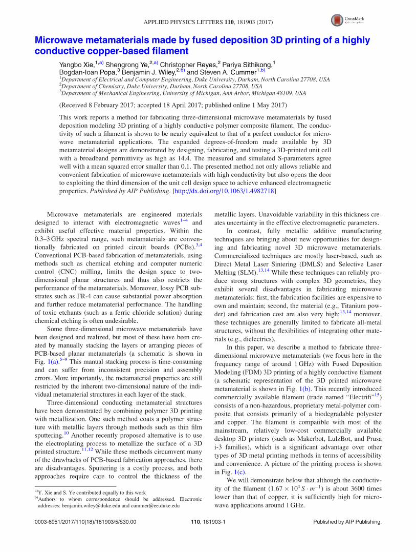
In this paper, we describe a method to fabricate three-
dimensional microwave metamaterials (we focus here in the
frequency range of around 1 GHz) with Fused Deposition
Modeling (FDM) 3D printing of a highly conductive filament
(a schematic representation of the 3D printed microwave
metamaterial is shown in Fig. 1(b). This recently introduced
commercially available filament (trade named “Electrifi”15)
consists of a non-hazardous, proprietary metal-polymer com-
posite that consists primarily of a biodegradable polyester
and copper. The filament is compatible with most of the
mainstream, relatively low-cost commercially available
desktop 3D printers (such as Makerbot, LulzBot, and Prusa
i-3 families), which is a significant advantage over other
types of 3D metal printing methods in terms of accessibility
and convenience. A picture of the printing process is shown
in Fig. 1(c).
We will demonstrate below that although the conductiv-
ity of the filament (1:67� 104 S � m�1) is about 3600 times
lower than that of copper, it is sufficiently high for micro-
wave applications around 1 GHz.
a)Y. Xie and S. Ye contributed equally to this workb)Authors to whom correspondence should be addressed. Electronic
addresses: [email protected] and [email protected]
0003-6951/2017/110(18)/181903/5/$30.00 Published by AIP Publishing.110, 181903-1
APPLIED PHYSICS LETTERS 110, 181903 (2017)
The characterization of a material as “highly con-
ductive” depends to a large extent on the operating frequency
range. When driven by an electric field, a highly conductive
material should allow unfettered electron flow through a
“skin depth” layer, whose depth can be expressed as
dskin ¼ffiffiffiffiffiffiffiffi
2l0xr
q, where the free space permeability l0 � 1:26
�10�6 H � m�1. The skin depth, dependent on both the
conductivity r and the frequency x, needs to satisfy16 dskin
k0
¼ 1pc0
ffiffiffiffiffiffiffix
2l0r
q� 1so that in its dispersion relation k2 ¼ l0x
2e
þ il0xr, the imaginary part will dominate the right-hand-
side. For example, a PCB with a 1=2 oz copper layer has a
trace thickness of 18 microns, and its skin depth at 1 GHz is
about 2 microns (assuming that the copper has a conductivity
of 5:96� 107S/m), the value dskin
k0� 6:7� 10�6 � 1, and
thus, the copper trace can be regarded as a high conductivity
structure around this frequency. However, the requirement
on the conductivity can be much less stringent as long as the
value dskin
k0is two orders-of-magnitude smaller than unity (as
confirmed with our numerical studies). For example, if we
desire dskin
k0< 0:53%, a conductivity of more than 100 S/m
would be sufficient.
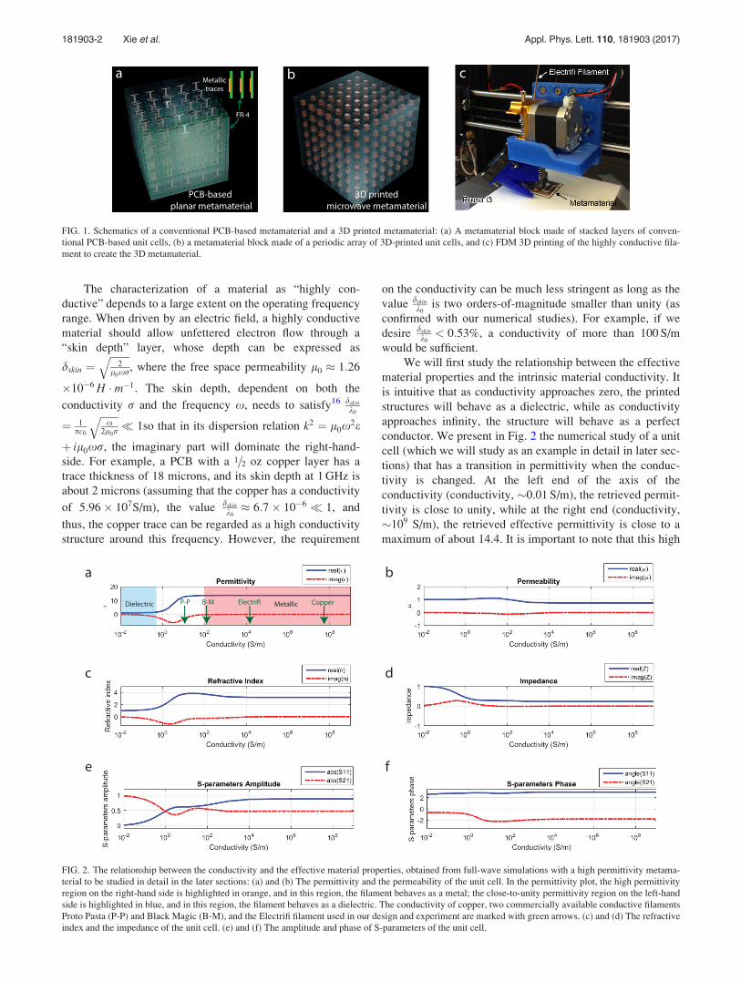
We will first study the relationship between the effective
material properties and the intrinsic material conductivity. It
is intuitive that as conductivity approaches zero, the printed
structures will behave as a dielectric, while as conductivity
approaches infinity, the structure will behave as a perfect
conductor. We present in Fig. 2 the numerical study of a unit
cell (which we will study as an example in detail in later sec-
tions) that has a transition in permittivity when the conduc-
tivity is changed. At the left end of the axis of the
conductivity (conductivity, �0.01 S/m), the retrieved permit-
tivity is close to unity, while at the right end (conductivity,
�109 S/m), the retrieved effective permittivity is close to a
maximum of about 14.4. It is important to note that this high
FIG. 2. The relationship between the conductivity and the effective material properties, obtained from full-wave simulations with a high permittivity metama-
terial to be studied in detail in the later sections: (a) and (b) The permittivity and the permeability of the unit cell. In the permittivity plot, the high permittivity
region on the right-hand side is highlighted in orange, and in this region, the filament behaves as a metal; the close-to-unity permittivity region on the left-hand
side is highlighted in blue, and in this region, the filament behaves as a dielectric. The conductivity of copper, two commercially available conductive filaments
Proto Pasta (P-P) and Black Magic (B-M), and the Electrifi filament used in our design and experiment are marked with green arrows. (c) and (d) The refractive
index and the impedance of the unit cell. (e) and (f) The amplitude and phase of S-parameters of the unit cell.
FIG. 1. Schematics of a conventional PCB-based metamaterial and a 3D printed metamaterial: (a) A metamaterial block made of stacked layers of conven-
tional PCB-based unit cells, (b) a metamaterial block made of a periodic array of 3D-printed unit cells, and (c) FDM 3D printing of the highly conductive fila-
ment to create the 3D metamaterial.
181903-2 Xie et al. Appl. Phys. Lett. 110, 181903 (2017)
effective permittivity remains relatively constant over sev-
eral orders of magnitude of electric conductivity. As bench-
marks, we annotate in Fig. 2(a) the conductivity of several
materials: copper, the Electrifi conductive filament used in
our experiment, and two other commercially available con-
ductive filaments Proto Pasta and Black Magic. These results
show that conductivity above roughly 102 S/m is required to
achieve a strong and low-loss metamaterial response at
1 GHz.
The ability to conveniently and reliably 3D print using a
sufficiently conductive filament provides extended degrees-
of-freedom for metamaterial designs. Different from conven-
tional PCB-based metamaterial designs that are restricted to
planar structures and assembly, 3D designs can achieve
larger charge storage surface areas, thicker current conduct-
ing channels, and complex 3D geometries to expand meta-
material responses to polarization and the angle of incidence.
We demonstrate below a design example that exploits the
extra spatial dimension to achieve enhanced broadband
dielectric responses.
Dielectric metamaterial particles are desired for many
wave controlling devices such as lenses7 and transformation
optics-based devices.17,18 One way to realize a strong dielec-
tric response is to use resonant metamaterials to create an
electric-field driven electric dipole response, e.g., with elec-
tric-field-coupled resonators.19 However, if the broad band-
width or low loss are desired, non-resonant broadband
metamaterials are typically required. One of the typical
broadband dielectric metamaterials is the so-called I-beam
metamaterial,17 which can be modeled as a series LC circuit.
The electric permittivity originates from the capacitance of
the structure, which generates an electrically driven electric
dipole moment. The relationship between the effective per-
mittivity and the local dipole moments in the unit cell can be
expressed as
eeff ¼D
e0E0
¼ 1þ P
e0E0
¼ 1þ 1
e0E0Vuc
ðVuc
p r*ð Þd3r
*; (1)
where pðr*Þ ¼ qðr*Þðr0* � r
*Þ is the local dipole moment and
ðr0* � r
*Þ is the displacement vector, and Vuc is the total vol-
ume of the unit cell.
In order to increase the value of the effective permittiv-
ity, we would like to increase the integral of the local dipole
moment pðr*Þ in the volume of the unit cell. While the charge
density qðr*Þ is roughly fixed for a given external electric
field E0, according to Gauss’s Law, the overall value of the
integral can be effectively enhanced by engineering the local
displacement vectors ðr0* � r
*Þ (i.e., the geometry) of the
structure. More specifically, a 3D unit cell designed with a
larger effective surface area will create larger local dipole
moments within the unit cell.
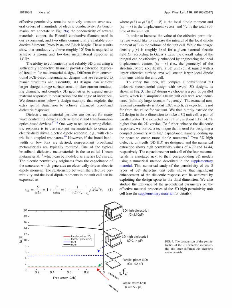
To verify this idea, we compare a conventional 2D
dielectric metamaterial design with several 3D designs, as
shown in Fig. 3. The 2D design we choose is a pair of parallel
wires, which is a simplified I-beam unit cell with zero induc-
tance (infinitely large resonant frequency). The extracted non-
resonant permittivity is about 1.02, which, as expected, is not
far from the value for vacuum. We then simply extrude the
2D design in the z-dimension to make a 3D unit cell: a pair of
parallel plates. The extracted permittivity is about 1.17, 14.7%
higher than the 2D version. To further enhance the dielectric
responses, we borrow a technique that is used for designing a
compact geometry with high capacitance, namely, coiling up
the space to create more dipole moments.9 Two 3D high
dielectric unit cells (3D HD) are designed, and the numerical
extraction shows high permittivity values of 4.79 and 14.44,
respectively. The capacitance per unit cell of the four metama-
terials is annotated next to their corresponding 3D models
using a numerical method described in the supplementary
material. This numerical study of the permittivity of the 3
types of 3D dielectric unit cells shows that significant
enhancement of the dielectric response can be achieved by
exploiting the design space in the third dimension. We also
studied the influence of the geometrical parameters on the
effective material properties of the 3D high-permittivity unit
cell (see the supplementary material for details).
FIG. 3. The comparison of the permit-
tivities of the 2D dielectric metamate-
rial and three different 3D dielectric
metamaterials.
181903-3 Xie et al. Appl. Phys. Lett. 110, 181903 (2017)
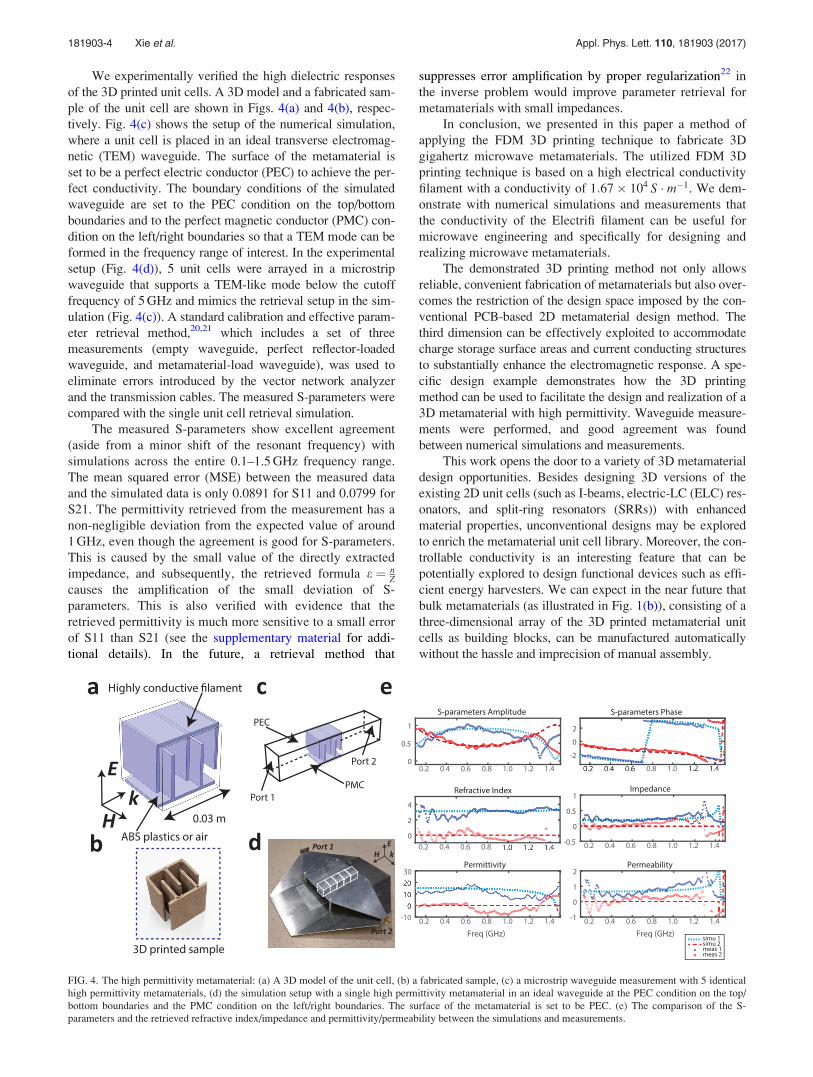
We experimentally verified the high dielectric responses
of the 3D printed unit cells. A 3D model and a fabricated sam-
ple of the unit cell are shown in Figs. 4(a) and 4(b), respec-
tively. Fig. 4(c) shows the setup of the numerical simulation,
where a unit cell is placed in an ideal transverse electromag-
netic (TEM) waveguide. The surface of the metamaterial is
set to be a perfect electric conductor (PEC) to achieve the per-
fect conductivity. The boundary conditions of the simulated
waveguide are set to the PEC condition on the top/bottom
boundaries and to the perfect magnetic conductor (PMC) con-
dition on the left/right boundaries so that a TEM mode can be
formed in the frequency range of interest. In the experimental
setup (Fig. 4(d)), 5 unit cells were arrayed in a microstrip
waveguide that supports a TEM-like mode below the cutoff
frequency of 5 GHz and mimics the retrieval setup in the sim-
ulation (Fig. 4(c)). A standard calibration and effective param-
eter retrieval method,20,21 which includes a set of three
measurements (empty waveguide, perfect reflector-loaded
waveguide, and metamaterial-load waveguide), was used to
eliminate errors introduced by the vector network analyzer
and the transmission cables. The measured S-parameters were
compared with the single unit cell retrieval simulation.
The measured S-parameters show excellent agreement
(aside from a minor shift of the resonant frequency) with
simulations across the entire 0.1–1.5 GHz frequency range.
The mean squared error (MSE) between the measured data
and the simulated data is only 0.0891 for S11 and 0.0799 for
S21. The permittivity retrieved from the measurement has a
non-negligible deviation from the expected value of around
1 GHz, even though the agreement is good for S-parameters.
This is caused by the small value of the directly extracted
impedance, and subsequently, the retrieved formula e ¼ nZ
causes the amplification of the small deviation of S-
parameters. This is also verified with evidence that the
retrieved permittivity is much more sensitive to a small error
of S11 than S21 (see the supplementary material for addi-
tional details). In the future, a retrieval method that
suppresses error amplification by proper regularization22 in
the inverse problem would improve parameter retrieval for
metamaterials with small impedances.
In conclusion, we presented in this paper a method of
applying the FDM 3D printing technique to fabricate 3D
gigahertz microwave metamaterials. The utilized FDM 3D
printing technique is based on a high electrical conductivity
filament with a conductivity of 1:67� 104 S � m�1. We dem-
onstrate with numerical simulations and measurements that
the conductivity of the Electrifi filament can be useful for
microwave engineering and specifically for designing and
realizing microwave metamaterials.
The demonstrated 3D printing method not only allows
reliable, convenient fabrication of metamaterials but also over-
comes the restriction of the design space imposed by the con-
ventional PCB-based 2D metamaterial design method. The
third dimension can be effectively exploited to accommodate
charge storage surface areas and current conducting structures
to substantially enhance the electromagnetic response. A spe-
cific design example demonstrates how the 3D printing
method can be used to facilitate the design and realization of a
3D metamaterial with high permittivity. Waveguide measure-
ments were performed, and good agreement was found
between numerical simulations and measurements.
This work opens the door to a variety of 3D metamaterial
design opportunities. Besides designing 3D versions of the
existing 2D unit cells (such as I-beams, electric-LC (ELC) res-
onators, and split-ring resonators (SRRs)) with enhanced
material properties, unconventional designs may be explored
to enrich the metamaterial unit cell library. Moreover, the con-
trollable conductivity is an interesting feature that can be
potentially explored to design functional devices such as effi-
cient energy harvesters. We can expect in the near future that
bulk metamaterials (as illustrated in Fig. 1(b)), consisting of a
three-dimensional array of the 3D printed metamaterial unit
cells as building blocks, can be manufactured automatically
without the hassle and imprecision of manual assembly.
FIG. 4. The high permittivity metamaterial: (a) A 3D model of the unit cell, (b) a fabricated sample, (c) a microstrip waveguide measurement with 5 identical
high permittivity metamaterials, (d) the simulation setup with a single high permittivity metamaterial in an ideal waveguide at the PEC condition on the top/
bottom boundaries and the PMC condition on the left/right boundaries. The surface of the metamaterial is set to be PEC. (e) The comparison of the S-
parameters and the retrieved refractive index/impedance and permittivity/permeability between the simulations and measurements.
181903-4 Xie et al. Appl. Phys. Lett. 110, 181903 (2017)
See supplementary material for the description of the
simulation method, the details about the employed highly
conductive filament, and other related discussions.
This work was partially supported by the
Multidisciplinary University Research Initiative grant from
the Office of Naval Research (No. N00014–13-1–0631).
B.J.W. and S.Y. have an equity interest in Multi3D
LLC, the manufacturer of Electrifi filament.
1C. Caloz and T. Itoh, Electromagnetic Metamaterials: Transmission LineTheory and Microwave Applications (John Wiley & Sons, 2005).
2Metamaterials: Physics and Engineering Explorations, edited by N.
Engheta and R. W. Ziolkowski (John Wiley & Sons, 2006).3D. R. Smith, J. B. Pendry, and M. C. Wiltshire, “Metamaterials and nega-
tive refractive index,” Science 305(5685), 788–792 (2004).4D. Schurig, J. J. Mock, B. J. Justice, S. A. Cummer, J. B. Pendry, A. F.
Starr, and D. R. Smith, “Metamaterial electromagnetic cloak at microwave
frequencies,” Science 314(5801), 977–980 (2006).5M. Zedler, C. Caloz, and P. Russer, “A 3-D isotropic left-handed
metamaterial based on the rotated transmission-line matrix (TLM)
scheme,” IEEE Trans. Microwave Theory Tech. 55(12), 2930–2941
(2007).6M. J. Freire, R. Marques, and L. Jelinek, “Experimental demonstration of
a l¼� 1 metamaterial lens for magnetic resonance imaging,” Appl. Phys.
Lett. 93(23), 231108 (2008).7N. Kundtz and D. R. Smith, “Extreme-angle broadband metamaterial
lens,” Nat. Mater 9(2), 129–132 (2010).8C. M. Soukoulis and M. Wegener, “Past achievements and future chal-
lenges in the development of three-dimensional photonic metamaterials,”
Nat. Photonics 5(9), 523–530 (2011).
9Z. Liang, T. Feng, S. Lok, F. Liu, K. B. Ng, C. H. Chan, J. Wang, S. Han,
S. Lee, and J. Li, “Space-coiling metamaterials with double negativity and
conical dispersion,” Sci. Rep. 3, 1614 (2013).10I. M. Ehrenberg, S. E. Sarma, and B. I. Wu, “A three-dimensional self-sup-
porting low loss microwave lens with a negative refractive index,” J. Appl.
Phys. 112(7), 073114 (2012).11S. M. Rudolph and A. Grbic, “A broadband three-dimensionally isotropic
negative-refractive-index medium,” IEEE Trans. Antennas. Propag. 60(8),
3661–3669 (2012).12R. Zhu and D. Marks, “Rapid prototyping lightweight millimeter wave antenna
and waveguide with copper plating,” in 40th International Conference on
Infrared, Millimeter, and Terahertz Waves (IRMMW-THz) (2015).13I. Gibson, D. Rosen, and B. Stucker, Additive Manufacturing Technologies:
3D Printing, Rapid Prototyping, and Direct Digital Manufacturing(Springer, 2014).
14H. Lipson and M. Kurman, Fabricated: The New World of 3D Printing(John Wiley & Sons, 2013).
15See https://www.multi3dllc.com (2017) for further information about
Electrifi filament.16R. Fitzpatrick, Maxwell’s Equations and the Principles of
Electromagnetism (Jones & Bartlett Publishers, 2008).17R. Liu, C. Ji, J. J. Mock, J. Y. Chin, T. J. Cui, and D. R. Smith,
“Broadband ground-plane cloak,” Science 323(5912), 366–369 (2009).18H. Chen, C. T. Chan, and P. Sheng, “Transformation optics and meta-
materials,” Nat. Mater. 9(5), 387–396 (2010).19D. Schurig, J. J. Mock, and D. R. Smith, “Electric-field-coupled resonators
for negative permittivity metamaterials,” Appl. Phys. Lett. 88(4), 041109
(2006).20X. Chen, T. M. Grzegorczyk, B. I. Wu, J. Pacheco, Jr., and J. A. Kong,
“Robust method to retrieve the constitutive effective parameters of meta-
materials,” Phys. Rev. E 70(1), 016608 (2004).21T. H. Hand, “Design and applications of frequency tunable and reconfigur-
able metamaterials,” Doctoral dissertation (Duke University, 2009).22R. C. Aster, B. Borchers, and C. H. Thurber, Parameter Estimation and
Inverse Problems (Elsevier Academic, 2005).
181903-5 Xie et al. Appl. Phys. Lett. 110, 181903 (2017)


![Influence of Thickness on the Structural, Morphological and Optical Properties … · 2021. 4. 27. · shown the improved selectivity of nitrogen from water [22-27]. Various deposition](https://img.pdfslide.fr/doc/110x75/6138e6fba4cdb41a985b5b90/influence-of-thickness-on-the-structural-morphological-and-optical-properties-2021.jpg)


![Indium Gallium diselenide (CIGS) · with efficiencies exceeding 18% [1 , 12, 13], electrodeposition, [14] and Physical vapor deposition (PVC)). [15] Cadmium Sulfide (CdS) thin film](https://img.pdfslide.fr/doc/110x75/5f7f2940f91f426f3d0ebcd9/indium-gallium-diselenide-cigs-with-efficiencies-exceeding-18-1-12-13-electrodeposition.jpg)