Embed Size (px)
Citation preview
Sains Malaysiana 42(2)(2013): 187–192
Fabrication and Transport Performance Characterization of Chemically-Doped Three-branch Junction Graphene Device
(Fabrikasi dan Ciri Prestasi Angkutan Peranti Grafin Berstruktur Tiga Cabang yang Didop Secara Kimia)
Shaharin FaDzli aBD rahMan*, Seiya KaSai & aBDul ManaF haShiM
ABSTRACT
A graphene-based three-branch nanojunction (TBJ) device having nanowire width of 200 nm was successfully fabricated. The layer number of graphene prepared by mechanical exfoliation was determined using a simple optical contrast method which showed good agreement with theoretical value. n-type doping by Polyethylene imines (PEI) was done to control the position of Dirac point. Baking and PEI doping was found to decrease contact resistance and increase the carrier mobility. The chemically-doped TBJ graphene showed carrier mobility of 20000 cm2/Vs, which gave related mean free path of 175 nm.
Keywords: Chemical doping; graphene; three-branch junction device
ABSTRAK
Peranti berstruktur tiga cabang (TBJ) daripada grafin yang mempunyai cabang selebar 200 nm telah berjaya difabrikasi. Bilangan lapisan grafin yang telah disediakan menggunakan kaedah pengelupasan secara mekanikal, telah ditentukan menggunakan kaedah kontras optik yang mudah dan keputusan uji kaji selari dengan nilai teori. Pendopan kepada jenis-n telah dibuat menggunakan polyethylene imines (PEI) untuk mengawal kedudukan titik Dirac. Pemanasan dan pendopan oleh PEI didapati telah merendahkan rintangan sentuhan logam dan menaikkan mobiliti pembawa. Grafin TBJ yang didop secara kimia telah menunjukkan mobiliti pembawa setinggi 20000 cm2/Vs, menjadikan purata laluan bebas sejauh 175 nm.
Kata kunci: Grafin; pendadahan secara kimia; peranti berstruktur tiga cabang
inTRoDuCTion
Three-branch junction (TBJ), a simple nanodevice consists of three nanowire branches (Figure 1), is shown to exhibit a unique nonlinear voltage transfer characteristic even at room temperature (Xu 2001). Several studies associated the observed behaviour with ballistic transport of carriers along the input branches of the device and predicted high frequency operation of TBJ device (irie & Sobolewski 2010; Mateos et al. 2003). although the mechanism of the nonlinearity remains unclear (Kasai et al. 2008), experimental works which mainly focused on iii-V semiconductor-based high-electron-mobility-transistor (heMT) structure showed the TBJ potential for various device applications (abd rahman et al. 2009; Shorubalko et al. 2002; Worschech et al. 2002). recently, TBJ structure on graphene has been studied and demonstrated (Gockeritz et al. 2011; Jacobsen et al. 2010). The work was motivated by the superior carrier mobility of graphene, which enable ballistic transport even at micron-scale (Mayorov et al. 2011). Furthermore, the gate-controlled ambipolar transport in graphene is expected to increase the functionality of the TBJ device (Jacobsen et al. 2010). however, further theoretical and experimental study is needed to understand fundamental operation of the TBJ device for any practical applications.
in this paper, we present the fabrication process of graphene-based TBJ and evaluate the basic transport properties of the fabricated device. For graphene layer number identification, we adopted a simple optical contrast method using typical optical microscope. The fabricated device was then treated by polyethylene imines (Pei) to control the Dirac point (VDirac) and enhance the carrier mobility. For realization of TBJ operation at ballistic regime, evaluation on transport properties such as
input 1 (Vin) input 2 (–Vin)
Output 1 (Vout) nanowire junction
Vin
V out
FiGuRe 1. Schematic diagram and voltage transfer curve of TBJ device
188
contact resistance, carrier mobility and mean free path is important.
DeviCe FABRiCATion
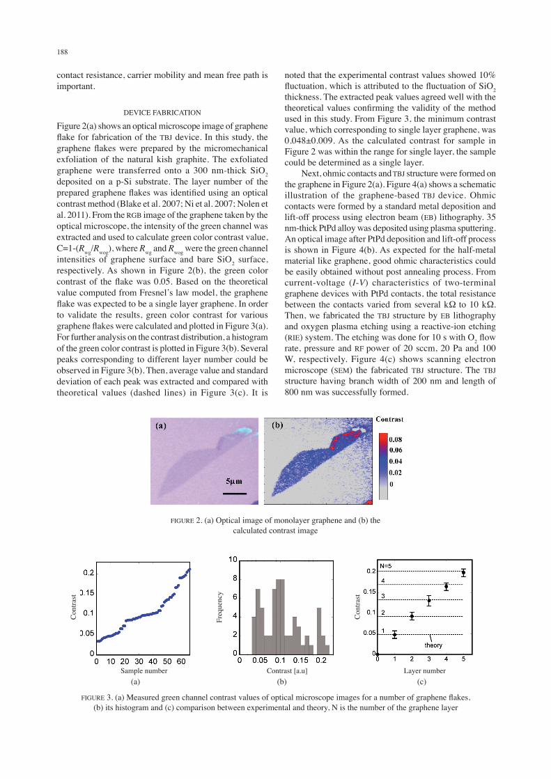
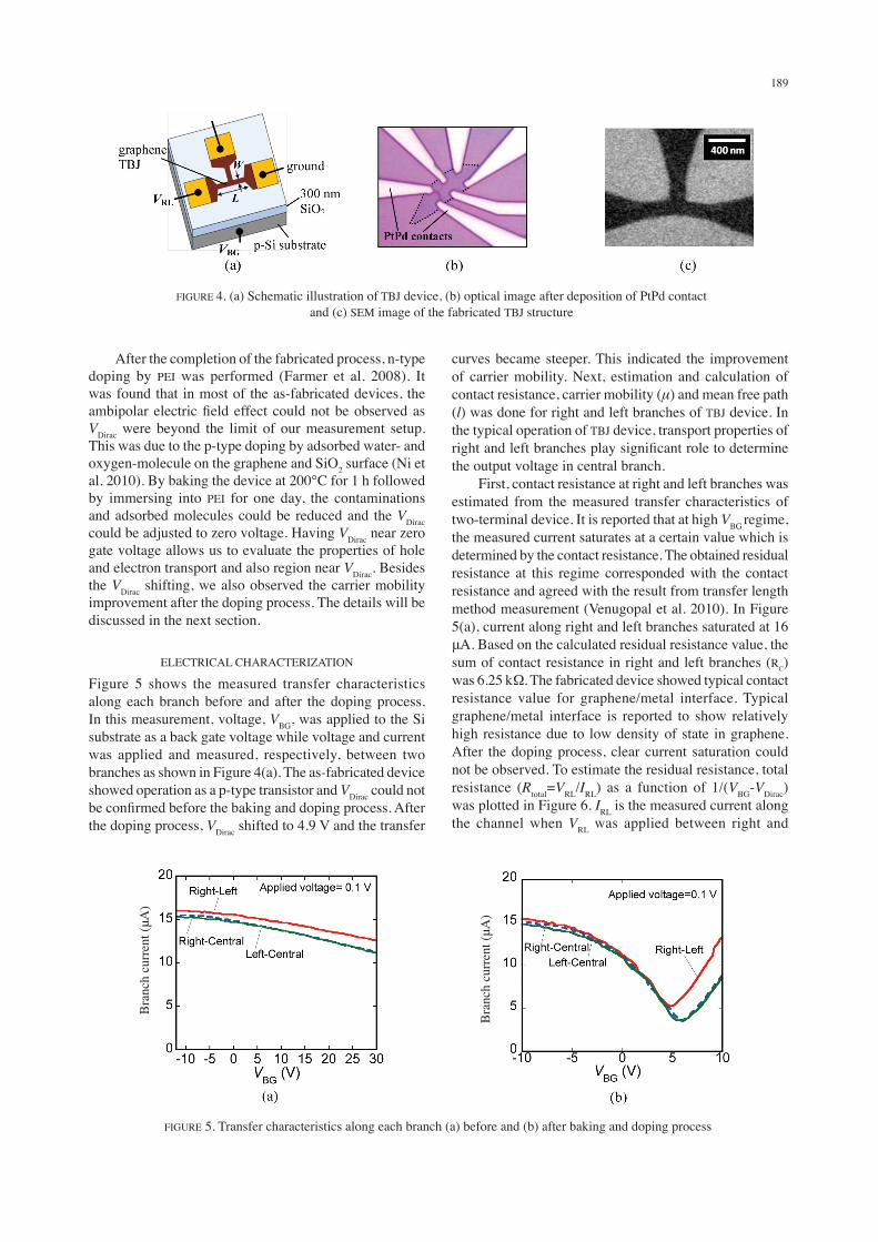
Figure 2(a) shows an optical microscope image of graphene flake for fabrication of the TBJ device. in this study, the graphene flakes were prepared by the micromechanical exfoliation of the natural kish graphite. The exfoliated graphene were transferred onto a 300 nm-thick SiO2 deposited on a p-Si substrate. The layer number of the prepared graphene flakes was identified using an optical contrast method (Blake et al. 2007; ni et al. 2007; nolen et al. 2011). From the RGB image of the graphene taken by the optical microscope, the intensity of the green channel was extracted and used to calculate green color contrast value, C=1-(Rwg/Rwog), where Rwg and Rwog were the green channel intensities of graphene surface and bare SiO2 surface, respectively. as shown in Figure 2(b), the green color contrast of the flake was 0.05. Based on the theoretical value computed from Fresnel’s law model, the graphene flake was expected to be a single layer graphene. in order to validate the results, green color contrast for various graphene flakes were calculated and plotted in Figure 3(a). For further analysis on the contrast distribution, a histogram of the green color contrast is plotted in Figure 3(b). Several peaks corresponding to different layer number could be observed in Figure 3(b). Then, average value and standard deviation of each peak was extracted and compared with theoretical values (dashed lines) in Figure 3(c). it is
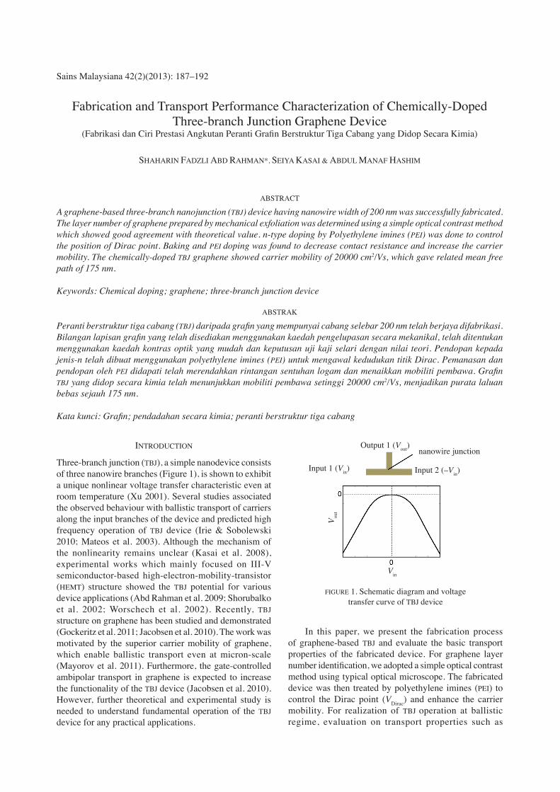
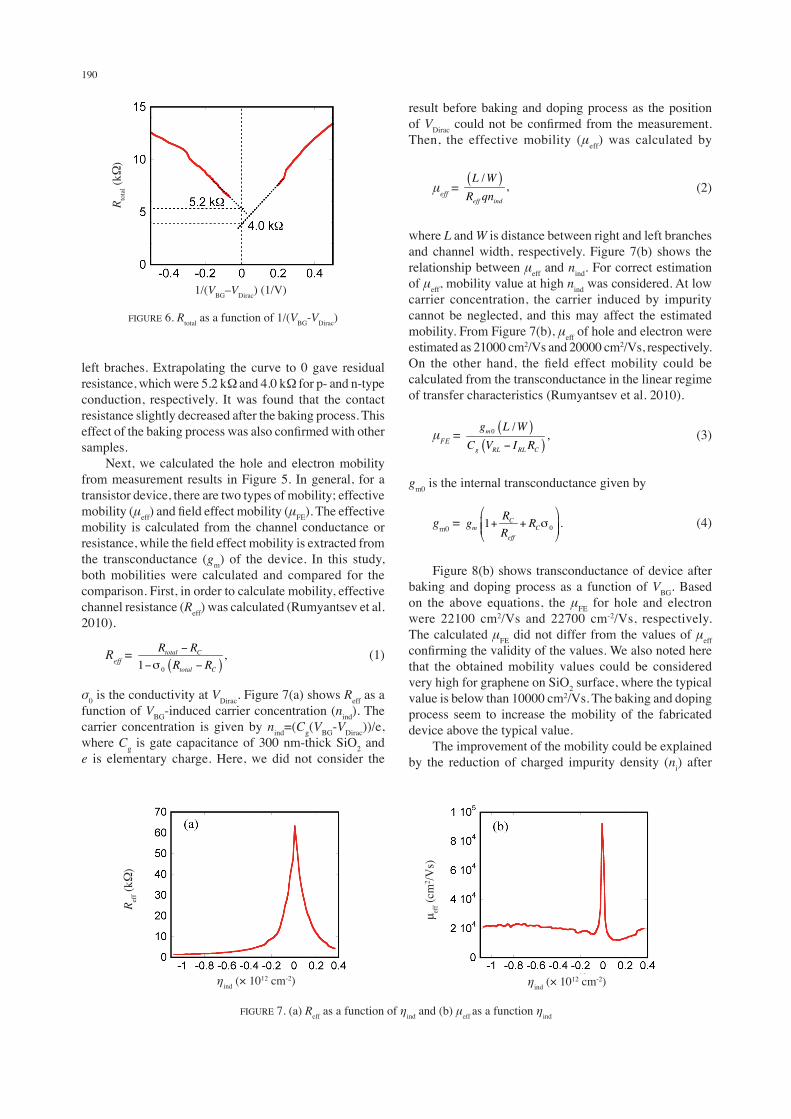
noted that the experimental contrast values showed 10% fluctuation, which is attributed to the fluctuation of Sio2 thickness. The extracted peak values agreed well with the theoretical values confirming the validity of the method used in this study. From Figure 3, the minimum contrast value, which corresponding to single layer graphene, was 0.048±0.009. as the calculated contrast for sample in Figure 2 was within the range for single layer, the sample could be determined as a single layer. next, ohmic contacts and TBJ structure were formed on the graphene in Figure 2(a). Figure 4(a) shows a schematic illustration of the graphene-based TBJ device. Ohmic contacts were formed by a standard metal deposition and lift-off process using electron beam (eB) lithography. 35 nm-thick PtPd alloy was deposited using plasma sputtering. an optical image after PtPd deposition and lift-off process is shown in Figure 4(b). as expected for the half-metal material like graphene, good ohmic characteristics could be easily obtained without post annealing process. From current-voltage (I-V) characteristics of two-terminal graphene devices with PtPd contacts, the total resistance between the contacts varied from several kΩ to 10 kΩ. Then, we fabricated the TBJ structure by eB lithography and oxygen plasma etching using a reactive-ion etching (rie) system. The etching was done for 10 s with O2 flow rate, pressure and rF power of 20 sccm, 20 Pa and 100 W, respectively. Figure 4(c) shows scanning electron microscope (SeM) the fabricated TBJ structure. The TBJ structure having branch width of 200 nm and length of 800 nm was successfully formed.
FiGuRe 2. (a) Optical image of monolayer graphene and (b) the calculated contrast image
(a) (b) (c)
FiGuRe 3. (a) Measured green channel contrast values of optical microscope images for a number of graphene flakes, (b) its histogram and (c) comparison between experimental and theory, n is the number of the graphene layer
Sample number Contrast [a.u] layer number
Con
trast
Freq
uenc
y
Con
trast
189
after the completion of the fabricated process, n-type doping by Pei was performed (Farmer et al. 2008). it was found that in most of the as-fabricated devices, the ambipolar electric field effect could not be observed as VDirac were beyond the limit of our measurement setup. This was due to the p-type doping by adsorbed water- and oxygen-molecule on the graphene and SiO2 surface (ni et al. 2010). By baking the device at 200°C for 1 h followed by immersing into Pei for one day, the contaminations and adsorbed molecules could be reduced and the VDirac could be adjusted to zero voltage. having VDirac near zero gate voltage allows us to evaluate the properties of hole and electron transport and also region near VDirac. Besides the VDirac shifting, we also observed the carrier mobility improvement after the doping process. The details will be discussed in the next section.
eleCTriCal CharaCTerizaTiOn
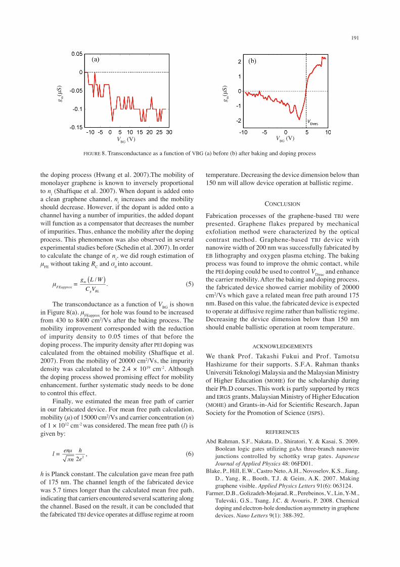
Figure 5 shows the measured transfer characteristics along each branch before and after the doping process. in this measurement, voltage, VBG, was applied to the Si substrate as a back gate voltage while voltage and current was applied and measured, respectively, between two branches as shown in Figure 4(a). The as-fabricated device showed operation as a p-type transistor and VDirac could not be confirmed before the baking and doping process. After the doping process, VDirac shifted to 4.9 V and the transfer
curves became steeper. This indicated the improvement of carrier mobility. next, estimation and calculation of contact resistance, carrier mobility (μ) and mean free path (l) was done for right and left branches of TBJ device. in the typical operation of TBJ device, transport properties of right and left branches play significant role to determine the output voltage in central branch. First, contact resistance at right and left branches was estimated from the measured transfer characteristics of two-terminal device. it is reported that at high VBG regime, the measured current saturates at a certain value which is determined by the contact resistance. The obtained residual resistance at this regime corresponded with the contact resistance and agreed with the result from transfer length method measurement (Venugopal et al. 2010). in Figure 5(a), current along right and left branches saturated at 16 μA. Based on the calculated residual resistance value, the sum of contact resistance in right and left branches (rC) was 6.25 kΩ. The fabricated device showed typical contact resistance value for graphene/metal interface. Typical graphene/metal interface is reported to show relatively high resistance due to low density of state in graphene. after the doping process, clear current saturation could not be observed. To estimate the residual resistance, total resistance (Rtotal=Vrl/Irl) as a function of 1/(VBG-VDirac) was plotted in Figure 6. Irl is the measured current along the channel when Vrl was applied between right and
FiGuRe 4. (a) Schematic illustration of TBJ device, (b) optical image after deposition of PtPd contact and (c) SeM image of the fabricated TBJ structure
FiGuRe 5. Transfer characteristics along each branch (a) before and (b) after baking and doping process
Bra
nch
curr
ent (
μA)
Bra
nch
curr
ent (
μA)
190
result before baking and doping process as the position of VDirac could not be confirmed from the measurement. Then, the effective mobility (μeff) was calculated by
μeff = (2) where L and W is distance between right and left branches and channel width, respectively. Figure 7(b) shows the relationship between μeff and nind. For correct estimation of μeff, mobility value at high nind was considered. at low carrier concentration, the carrier induced by impurity cannot be neglected, and this may affect the estimated mobility. From Figure 7(b), μeff of hole and electron were estimated as 21000 cm2/Vs and 20000 cm2/Vs, respectively. on the other hand, the field effect mobility could be calculated from the transconductance in the linear regime of transfer characteristics (rumyantsev et al. 2010).
μFE = (3) gm0 is the internal transconductance given by
gm0 = (4) Figure 8(b) shows transconductance of device after baking and doping process as a function of VBG. Based on the above equations, the μFe for hole and electron were 22100 cm2/Vs and 22700 cm-2/Vs, respectively. The calculated μFe did not differ from the values of μeff confirming the validity of the values. We also noted here that the obtained mobility values could be considered very high for graphene on SiO2 surface, where the typical value is below than 10000 cm2/Vs. The baking and doping process seem to increase the mobility of the fabricated device above the typical value. The improvement of the mobility could be explained by the reduction of charged impurity density (ni) after
1/(VBG–VDirac) (1/V)
R tota
l (kΩ
)
FiGuRe 6. Rtotal as a function of 1/(VBG-VDirac)
left braches. extrapolating the curve to 0 gave residual resistance, which were 5.2 kΩ and 4.0 kΩ for p- and n-type conduction, respectively. it was found that the contact resistance slightly decreased after the baking process. This effect of the baking process was also confirmed with other samples. next, we calculated the hole and electron mobility from measurement results in Figure 5. in general, for a transistor device, there are two types of mobility; effective mobility (μeff) and field effect mobility (μFe). The effective mobility is calculated from the channel conductance or resistance, while the field effect mobility is extracted from the transconductance (gm) of the device. in this study, both mobilities were calculated and compared for the comparison. First, in order to calculate mobility, effective channel resistance (Reff) was calculated (rumyantsev et al. 2010).
Reff = (1) σ0 is the conductivity at VDirac. Figure 7(a) shows Reff as a function of VBG-induced carrier concentration (nind). The carrier concentration is given by nind=(Cg(VBG-VDirac))/e, where Cg is gate capacitance of 300 nm-thick SiO2 and e is elementary charge. here, we did not consider the
ηind (× 1012 cm-2)
R eff (
kΩ)
ηind (× 1012 cm-2)
μ eff (
cm2 /V
s)
FiGuRe 7. (a) Reff as a function of ηind and (b) μeff as a function ηind
191
the doping process (hwang et al. 2007).The mobility of monolayer graphene is known to inversely proportional to ni (Shaffique et al. 2007). When dopant is added onto a clean graphene channel, ni increases and the mobility should decrease. however, if the dopant is added onto a channel having a number of impurities, the added dopant will function as a compensator that decreases the number of impurities. Thus, enhance the mobility after the doping process. This phenomenon was also observed in several experimental studies before (Schedin et al. 2007). in order to calculate the change of ni, we did rough estimation of μFe without taking RC and σ0 into account.
μFEapprox = (5) The transconductance as a function of VBG is shown in Figure 8(a). μFeapprox for hole was found to be increased from 430 to 8400 cm2/Vs after the baking process. The mobility improvement corresponded with the reduction of impurity density to 0.05 times of that before the doping process. The impurity density after Pei doping was calculated from the obtained mobility (Shaffique et al. 2007). From the mobility of 20000 cm2/Vs, the impurity density was calculated to be 2.4 × 1019 cm-2. although the doping process showed promising effect for mobility enhancement, further systematic study needs to be done to control this effect. Finally, we estimated the mean free path of carrier in our fabricated device. For mean free path calculation, mobility (μ) of 15000 cm2/Vs and carrier concentration (n) of 1 × 1012 cm-2 was considered. The mean free path (l) is given by:
l = μ
π (6)
h is Planck constant. The calculation gave mean free path of 175 nm. The channel length of the fabricated device was 5.7 times longer than the calculated mean free path, indicating that carriers encountered several scattering along the channel. Based on the result, it can be concluded that the fabricated TBJ device operates at diffuse regime at room
temperature. Decreasing the device dimension below than 150 nm will allow device operation at ballistic regime.
ConCluSion
Fabrication processes of the graphene-based TBJ were presented. Graphene flakes prepared by mechanical exfoliation method were characterized by the optical contrast method. Graphene-based TBJ device with nanowire width of 200 nm was successfully fabricated by eB lithography and oxygen plasma etching. The baking process was found to improve the ohmic contact, while the Pei doping could be used to control VDirac and enhance the carrier mobility. after the baking and doping process, the fabricated device showed carrier mobility of 20000 cm2/vs which gave a related mean free path around 175 nm. Based on this value, the fabricated device is expected to operate at diffusive regime rather than ballistic regime. Decreasing the device dimension below than 150 nm should enable ballistic operation at room temperature.
ACKnoWleDGeMenTS
We thank Prof. Takashi Fukui and Prof. Tamotsu hashizume for their supports. S.F.a. rahman thanks universiti Teknologi Malaysia and the Malaysian Ministry of higher education (MOhe) for the scholarship during their Ph.D courses. This work is partly supported by FrGS and erGS grants, Malaysian Ministry of higher education (MOhe) and Grants-in-Aid for Scientific Research, Japan Society for the Promotion of Science (JSPS).
reFerenCeS
Abd Rahman, S.F., nakata, D., Shiratori, Y. & Kasai, S. 2009. Boolean logic gates utilizing gaAs three-branch nanowire junctions controlled by schottky wrap gates. Japanese Journal of Applied Physics 48: 06FD01.
Blake, P., Hill, e.W., Castro neto, A.H., novoselov, K.S., Jiang, D., Yang, R., Booth, T.J. & Geim, A.K. 2007. Making graphene visible. Applied Physics Letters 91(6): 063124.
Farmer, D.B., Golizadeh-Mojarad, R., Perebeinos, v., lin, Y-M., Tulevski, G.S., Tsang, J.C. & avouris, P. 2008. Chemical doping and electron-hole donduction asymmetry in graphene devices. Nano Letters 9(1): 388-392.
FiGuRe 8. Transconductance as a function of vBG (a) before (b) after baking and doping process
VBG (V)
g m(μ
S)
VBG (V)
g m(μ
S)
192
Gockeritz, r., Pezoldt, J. & Schwierz, F. 2011. epitaxial graphene three-terminal junctions. Applied Physics Letters 99(17): 173111.
hwang, e.h., adam, S. & Das Sarma, S. 2007. Transport in chemically doped graphene in the presence of adsorbed molecules. Physical Review B 76(19): 195421.
irie, h. & Sobolewski, r. 2010. Terahertz electrical response of nanoscale three-branch junctions. Journal of Applied Physics 107(8): 084315.
Jacobsen, A., Shorubalko, i., Maag, l., Sennhauser, u. & ensslin, K. 2010. Rectification in three-terminal graphene junctions. Applied Physics Letters 97(3): 032110.
Kasai, S., nakamura, T., Abd Rahman, S.F. & Shiratori, Y. 2008. Study on nonlinear electrical characteristics of gaas-based three-branch nanowire junctions controlled by schottky wrap gates. Japanese Journal of Applied Physics 47: 4958.
Mateos, J., vasallo, B.G., Pardo, D., Gonzalez, T., Galloo, J.S., Bollaert, S., Roelens, Y. & Cappy, A. 2003. Microscopic modeling of nonlinear transport in ballistic nanodevices. Electron Devices, IEEE Transactions on 50(9): 1897-1905.
Mayorov, A.S., Gorbachev, R.v., Morozov, S.v., Britnell, l., Rashid J., Ponomarenko, l.A., Blake, P., novoselov, K.S., Watanabe, K., Taniguchi, T. & Geim, A.K. 2011. Micrometer-scale ballistic transport in encapsulated graphene at room temperature. Nano Letters 11(6): 2396-2399.
ni, Z.H., Wang, H.M., Kasim, J., Fan, H.M., Yu, T., Wu, y.h., Feng, y.P. & Shen, z.X. 2007. Graphene thickness determination using reflection and contrast spectroscopy. Nano Letters 7(9): 2758-2763.
ni, z.h., Wang, h.M., luo, z.Q., Wang, y.y., yu, T., Wu, y.h. & Shen, z.X. 2010. The effect of vacuum annealing on graphene. Journal of Raman Spectroscopy 41(5): 479-483.
nolen, C.M., Denina, G., Teweldebrhan, D., Bhanu, B. & Balandin, A.A. 2011. High-throughput large-area automated identification and quality control of graphene and few-layer graphene films. ACS Nano 5(2): 914-922.
Rumyantsev, S., liu, G., Stillman, W., Shur, M. & Balandin, a.a. 2010. electrical and noise characteristics of graphene field-effect transistors: ambient effects, noise sources and physical mechanisms. Journal of Physics: Condensed Matter 22(39): 395302.
Schedin, F., Geim, A.K., Morozov, S.v., Hill, e.W., Blake, P., Katsnelson, M.i. & novoselov, K.S. 2007. Detection of individual gas molecules adsorbed on graphene. Nature Materials 6(9): 652-655.
Shaffique, A., Hwang, e.H., Galitski, v.M. & Das Sarma, S. 2007. a self-consistent theory for graphene transport. Proceedings of the National Academy of Sciences of the United States of America 104(47): 18392-18397.
Shorubalko, i., Xu, h.Q., Maximov, i., nilsson, D., Omling, r., Samuelson, l. & Seifert. W. 2002. a novel frequency-multiplication device based on three-terminal ballistic junction. Electron Device Letters, IEEE 23(7): 377-379.
Venugopal, a., Colombo, l. & Vogel, e.M. 2010. Contact resistance in few and multilayer graphene devices. Applied Physics Letters 96(1): 013512.
Worschech, l., Schliemann, a., reitzenstein, S., hartmann, P. & Forchel, A. 2002. Microwave rectification in ballistic nanojunctions at room temperature. Microelectronic Engineering 63(1-3): 217-221.
Xu, h.Q. 2001. electrical properties of three-terminal ballistic junctions. Applied Physics Letters 78(14): 2064-2066.
Shaharin Fadzli abd rahman*Faculty of electrical engineeringuniversiti Teknologi Malaysia81310 uTM Skudai, JohorMalaysia
Seiya KasaiGraduate School of information Science and Technologyand research Center for integrated Quantum electronics Hokkaido university n14, W9, Sapporo 060-0814 Japan
abdul Manaf hashimMalaysia-Japan international institute of Technology (MJiiT)universiti Teknologi Malaysia international CampusJalan Semarak 54100 Kuala lumpurMalaysia
*Corresponding author; email: [email protected]
received: 7 January 2012accepted: 21 May 2012