Embed Size (px)
Citation preview
L’Elettronica di Potenza come principale fattore abilitante dell'energia ecosostenibile
e della mobilità elettrica.
Ruolo di STMicroelectronics
F. Di Giovanni, G. Di Marco, F. Di Franco
STMicroelectronics
DIPARTIMENTO di
INGEGNERIA
ELETTRICA ELETTRONICA
E INFORMATICA
Giovedì 18 marzo 2021
14:30 – 16:00
Agenda
2
14:30 - 14:35 Introduzione al seminario (Prof. Rizzo, Prof. Scelba)
14:35 - 15:45 L'Elettronica di Potenza come principale fattore abilitante per una maggiore efficienza energetica (Ing. Di Giovanni, Ing. Di Franco, Ing. Di Marco)
▪ Breve video STMicroelectronics – Catania (Ing. Di Marco)
▪ Seminario – parte prima (Ing. Di Giovanni)
▪ Video (1) su tecnologia GaN (Ing. Di Marco)
▪ Seminario – seconda parte (Ing. Di Giovanni)
▪ Video (2) su esempi applicativi dell’elettronica di potenza (Ing. Di Franco)
▪ Domande dai partecipanti
15:45 - 16:00 Conclusioni
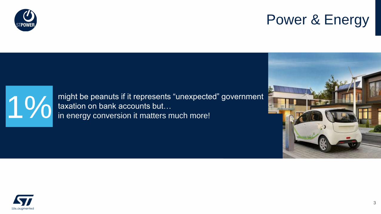
Power & Energy
3
might be peanuts if it represents “unexpected” government
taxation on bank accounts but…
in energy conversion it matters much more!1%
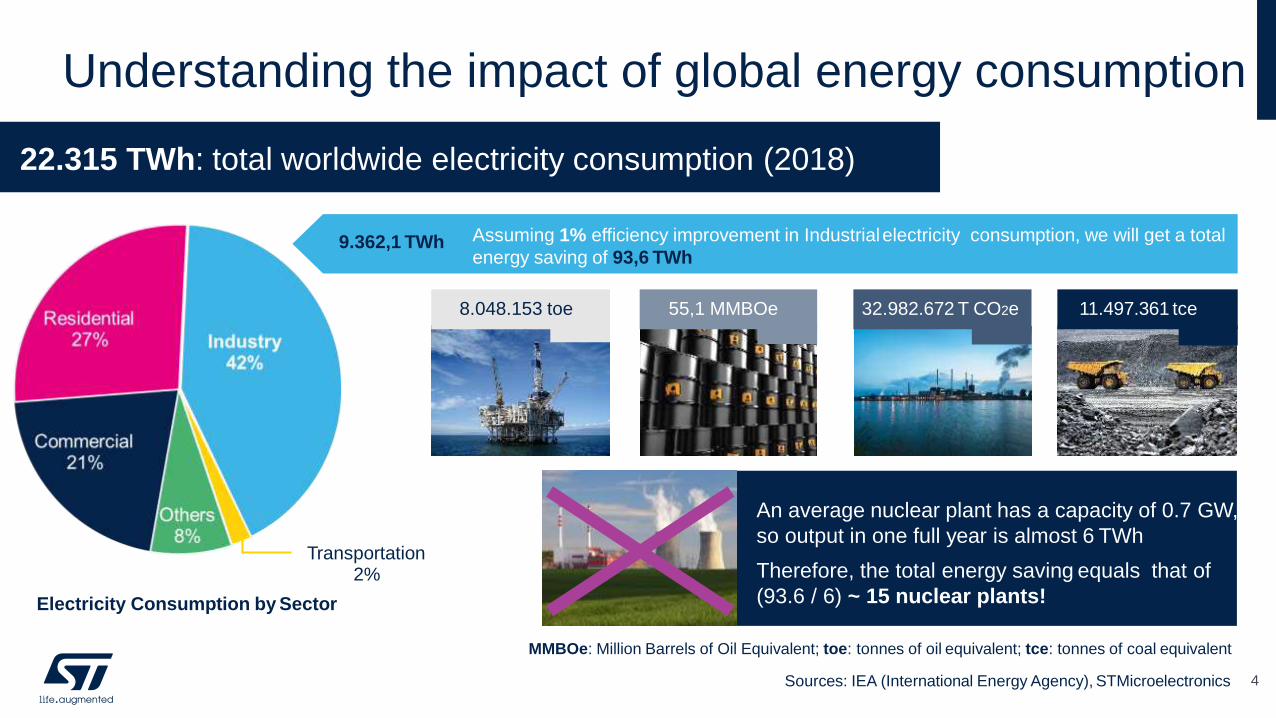
Understanding the impact of global energy consumption
Assuming 1% efficiency improvement in Industrialelectricity consumption, we will get a total
energy saving of 93,6 TWh
Sources: IEA (International Energy Agency), STMicroelectronics
Transportation 2%
Electricity Consumption by Sector
9.362,1 TWh
MMBOe: Million Barrels of Oil Equivalent; toe: tonnes of oil equivalent; tce: tonnes of coal equivalent
22.315 TWh: total worldwide electricity consumption (2018)
4
An average nuclear plant has a capacity of 0.7 GW,
so output in one full year is almost 6 TWh
Therefore, the total energy saving equals that of
(93.6 / 6) ~ 15 nuclear plants!
8.048.153 toe 55,1 MMBOe 32.982.672 T CO2e 11.497.361 tce
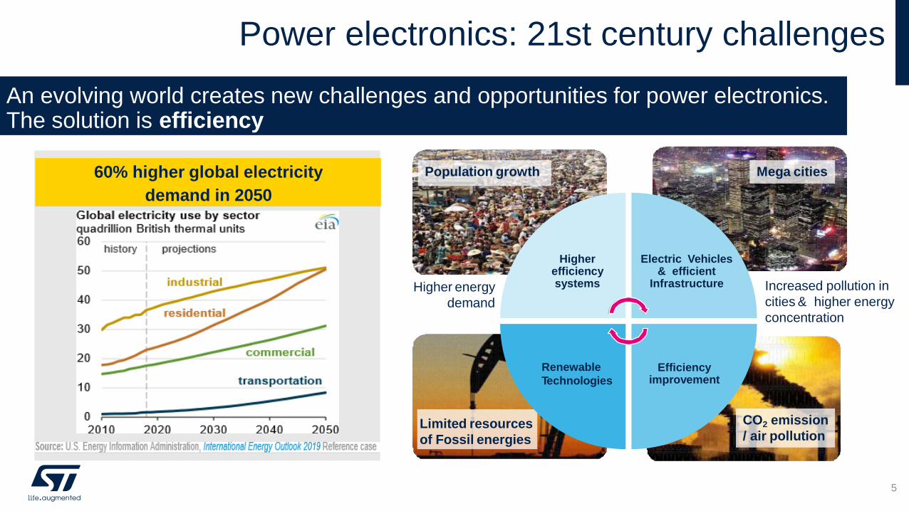
Power electronics: 21st century challenges
Higher efficiency systems
Electric Vehicles & efficient
Infrastructure
Efficiency improvement
Increased pollution in
cities & higher energy
concentration
Higher energy
demand
Population growth Mega cities
CO2 emission
/ air pollutionLimited resources
of Fossil energies
An evolving world creates new challenges and opportunities for power electronics. The solution is efficiency
60% higher global electricity
demand in 2050
5
Renewable
Technologies
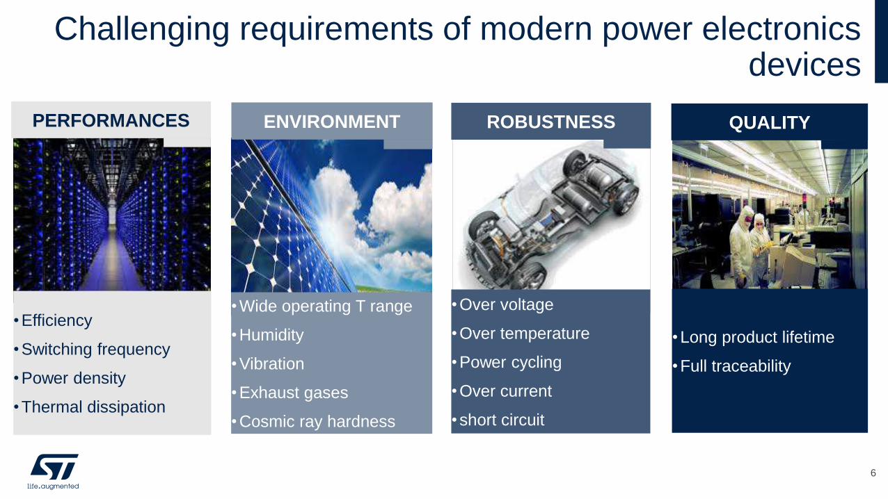
Challenging requirements of modern power electronics devices
6
•Efficiency
•Switching frequency
•Power density
•Thermal dissipation
PERFORMANCES
•Wide operating T range
•Humidity
•Vibration
•Exhaust gases
•Cosmic ray hardness
ENVIRONMENT
•Over voltage
•Over temperature
•Power cycling
•Over current
•short circuit
ROBUSTNESS
•Long product lifetime
•Full traceability
QUALITY
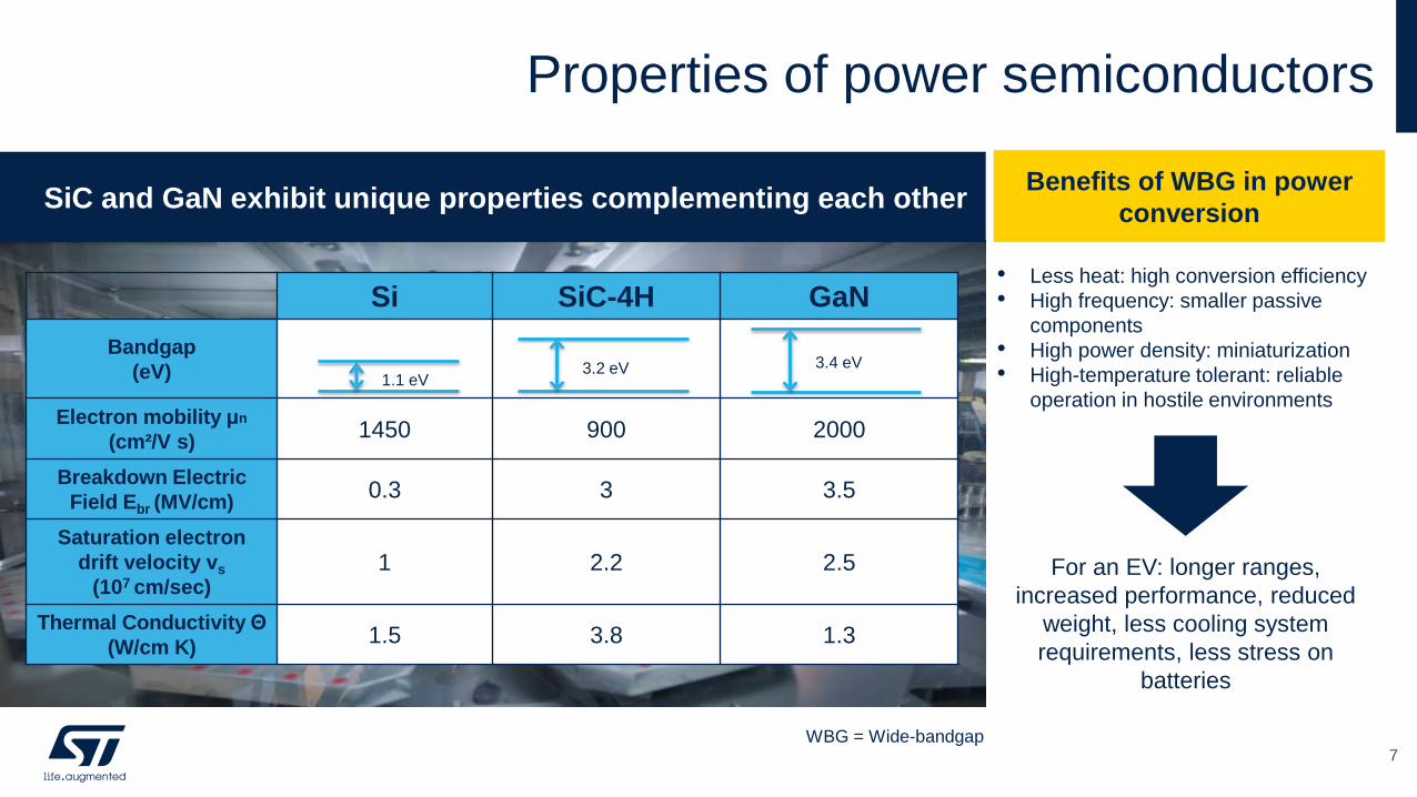
Properties of power semiconductors
7
SiC and GaN exhibit unique properties complementing each other
Si SiC-4H GaN
Bandgap
(eV)
Electron mobility μn
(cm²/V s)1450 900 2000
Breakdown Electric
Field Ebr (MV/cm)0.3 3 3.5
Saturation electron
drift velocity vs
(107 cm/sec)1 2.2 2.5
Thermal Conductivity Θ
(W/cm K)1.5 3.8 1.3
3.4 eV3.2 eV1.1 eV
Benefits of WBG in power
conversion
• Less heat: high conversion efficiency
• High frequency: smaller passive
components
• High power density: miniaturization
• High-temperature tolerant: reliable
operation in hostile environments
For an EV: longer ranges,
increased performance, reduced
weight, less cooling system
requirements, less stress on
batteries
WBG = Wide-bandgap
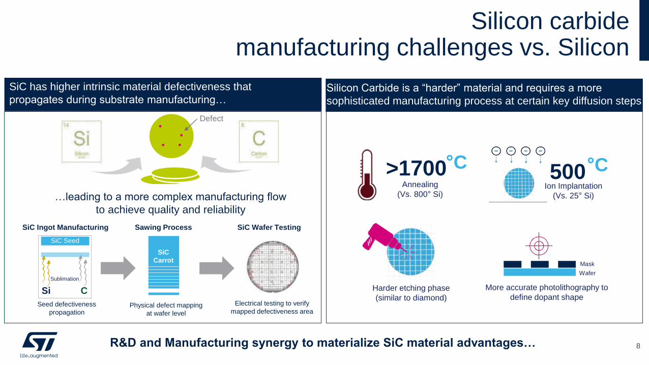
Silicon carbidemanufacturing challenges vs. Silicon
SiC has higher intrinsic material defectiveness that
propagates during substrate manufacturing…
…leading to a more complex manufacturing flow
to achieve quality and reliability
Annealing
(Vs. 800° Si)
>1700°CIon Implantation
(Vs. 25° Si)
500°C
Harder etching phase
(similar to diamond)
More accurate photolithography to
define dopant shape
Silicon Carbide is a “harder” material and requires a more
sophisticated manufacturing process at certain key diffusion steps
Wafer
Mask
Physical defect mapping
at wafer level
Electrical testing to verify
mapped defectiveness area
Defect
SiC Ingot Manufacturing Sawing Process
SiC
Carrot
Si C
SiC Seed
Sublimation
SiC Wafer Testing
Seed defectiveness
propagation
R&D and Manufacturing synergy to materialize SiC material advantages… 8
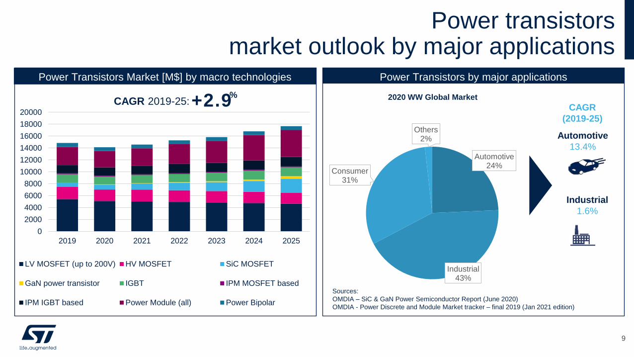
Power transistorsmarket outlook by major applications
Industrial
1.6%
Automotive
13.4%
Power Transistors Market [M$] by macro technologies
CAGR
(2019-25)
CAGR 2019-25:+ 2 . 9%
0
2000
4000
6000
8000
10000
12000
14000
16000
18000
20000
2019 2020 2021 2022 2023 2024 2025
LV MOSFET (up to 200V) HV MOSFET SiC MOSFET
GaN power transistor IGBT IPM MOSFET based
IPM IGBT based Power Module (all) Power Bipolar
Power Transistors by major applications
2020 WW Global Market
Sources:
OMDIA – SiC & GaN Power Semiconductor Report (June 2020)
OMDIA - Power Discrete and Module Market tracker – final 2019 (Jan 2021 edition)
Automotive24%
Industrial43%
Consumer31%
Others2%
9
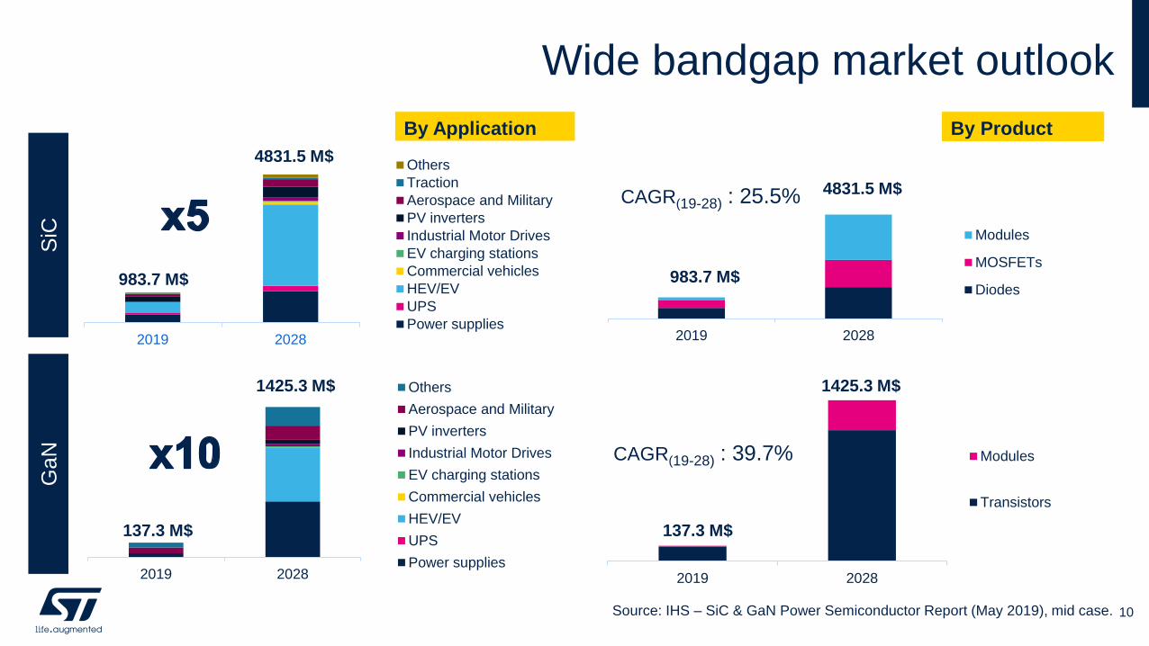
2019 2028
Modules
MOSFETs
Diodes
Wide bandgap market outlook
2019 2028
Others
Traction
Aerospace and Military
PV inverters
Industrial Motor Drives
EV charging stations
Commercial vehicles
HEV/EV
UPS
Power supplies
SiC
GaN
2019 2028
Others
Aerospace and Military
PV inverters
Industrial Motor Drives
EV charging stations
Commercial vehicles
HEV/EV
UPS
Power supplies
By Application By Product
2019 2028
Modules
Transistors
983.7 M$
4831.5 M$
CAGR(19-28) : 25.5%
983.7 M$
4831.5 M$
137.3 M$
1425.3 M$
CAGR(19-28) : 39.7%
137.3 M$
1425.3 M$
Source: IHS – SiC & GaN Power Semiconductor Report (May 2019), mid case. 10
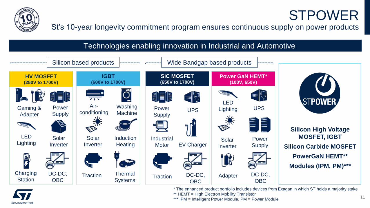
STPOWERSt’s 10-year longevity commitment program ensures continuous supply on power products
Industrial
Motor
HV MOSFET(250V to 1700V)
IGBT(600V to 1700V)
SiC MOSFET(650V to 1700V)
Technologies enabling innovation in Industrial and Automotive
Gaming &
Adapter
Charging
Station
LED
LightingSolar
Inverter
Air-
conditioningWashing
Machine
Solar
Inverter
Induction
Heating EV Charger
UPSPower
Supply
Traction Traction DC-DC,
OBC
DC-DC,
OBC
Thermal
Systems
Power GaN HEMT*(100V, 650V)
UPS
Power
Supply
DC-DC,
OBC
LED
Lighting
Solar
Inverter
Adapter
Power
Supply
Wide Bandgap based products Silicon based products
Silicon High Voltage
MOSFET, IGBT
Silicon Carbide MOSFET
PowerGaN HEMT**
Modules (IPM, PM)***
* The enhanced product portfolio includes devices from Exagan in which ST holds a majority stake
** HEMT = High Electron Mobility Transistor
*** IPM = Intelligent Power Module, PM = Power Module11
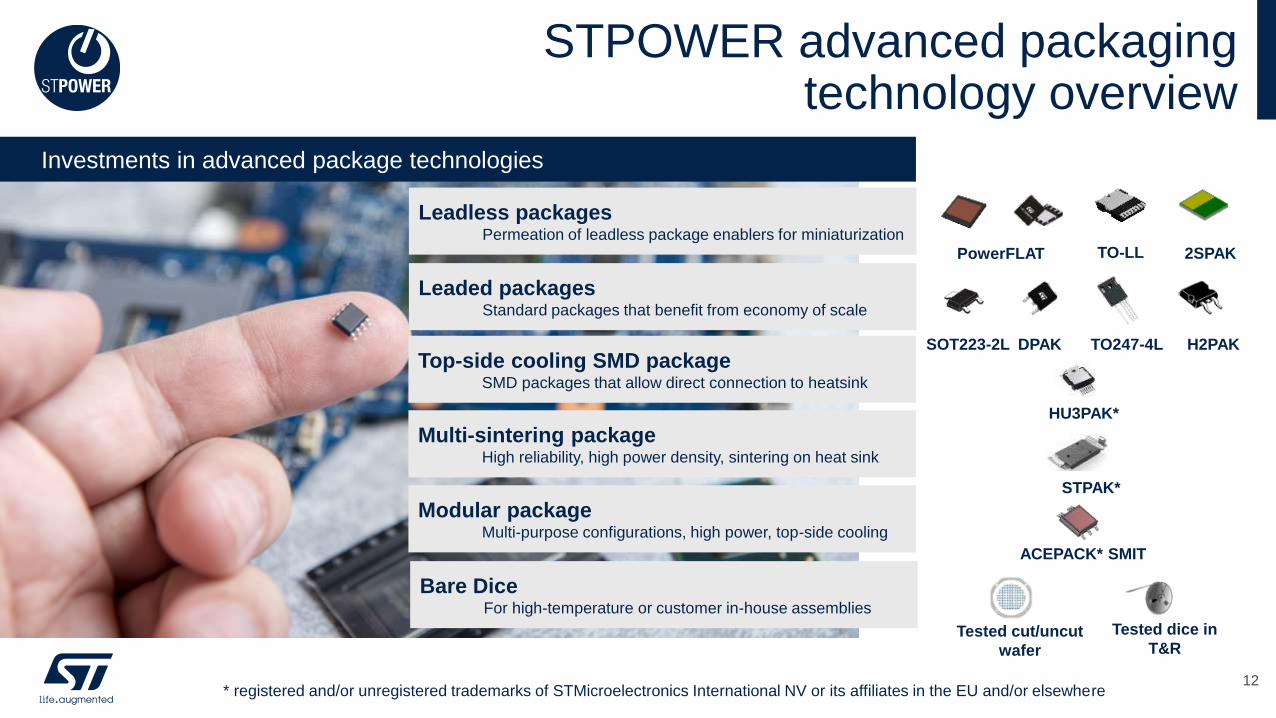
STPOWER advanced packagingtechnology overview
Investments in advanced package technologies
Leadless packagesPermeation of leadless package enablers for miniaturization
PowerFLAT
Bare Dice For high-temperature or customer in-house assemblies
Leaded packagesStandard packages that benefit from economy of scale
DPAK
Tested cut/uncut
wafer
Tested dice in
T&R
Top-side cooling SMD packageSMD packages that allow direct connection to heatsink
Multi-sintering packageHigh reliability, high power density, sintering on heat sink
Modular packageMulti-purpose configurations, high power, top-side cooling
HU3PAK*
STPAK*
ACEPACK* SMIT
TO-LL
TO247-4L H2PAKSOT223-2L
2SPAK
* registered and/or unregistered trademarks of STMicroelectronics International NV or its affiliates in the EU and/or elsewhere 12
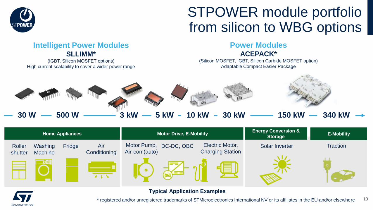
STPOWER module portfoliofrom silicon to WBG options
Home Appliances Motor Drive, E-MobilityEnergy Conversion &
Storage
Intelligent Power ModulesSLLIMM*
(IGBT, Silicon MOSFET options)
High current scalability to cover a wider power range
30 W 340 kW3 kW500 W 5 kW
Washing
Machine
Air
ConditioningFridge Electric Motor,
Charging Station
Motor Pump,
Air-con (auto)Solar Inverter
Power ModulesACEPACK*
(Silicon MOSFET, IGBT, Silicon Carbide MOSFET option)
Adaptable Compact Easier Package
E-Mobility
Typical Application Examples
Traction
150 kW10 kW 30 kW
DC-DC, OBCRoller
shutter
* registered and/or unregistered trademarks of STMicroelectronics International NV or its affiliates in the EU and/or elsewhere 13
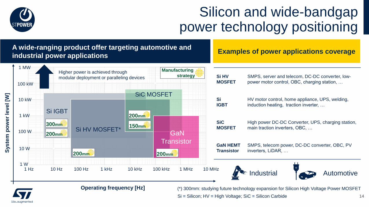
1 Hz 10 Hz 100 Hz 1 kHz 10 kHz 100 kHz 1 MHz 10 MHz
Higher power is achieved through
modular deployment or paralleling devices
Operating frequency [Hz]
Sys
tem
po
we
r le
ve
l [W
]
Si IGBT
Si HV MOSFET*
SiC MOSFET
GaN
Transistor
1 MW
100 kW
10 kW
1 kW
100 W
1 W
10 W
Silicon and wide-bandgappower technology positioning
A wide-ranging product offer targeting automotive and
industrial power applications
Manufacturing
strategy
200mm
200mm
200mm
150mm300mm
(*) 300mm: studying future technology expansion for Silicon High Voltage Power MOSFET
200mm
Examples of power applications coverage
Si = Silicon; HV = High Voltage; SiC = Silicon Carbide
Industrial Automotive
Si HV
MOSFET
SMPS, server and telecom, DC-DC converter, low-
power motor control, OBC, charging station, …
Si
IGBT
HV motor control, home appliance, UPS, welding,
induction heating, traction inverter, …
SiC
MOSFET
High power DC-DC Converter, UPS, charging station,
main traction inverters, OBC, …
GaN HEMT
Transistor
SMPS, telecom power, DC-DC converter, OBC, PV
inverters, LiDAR, …
14
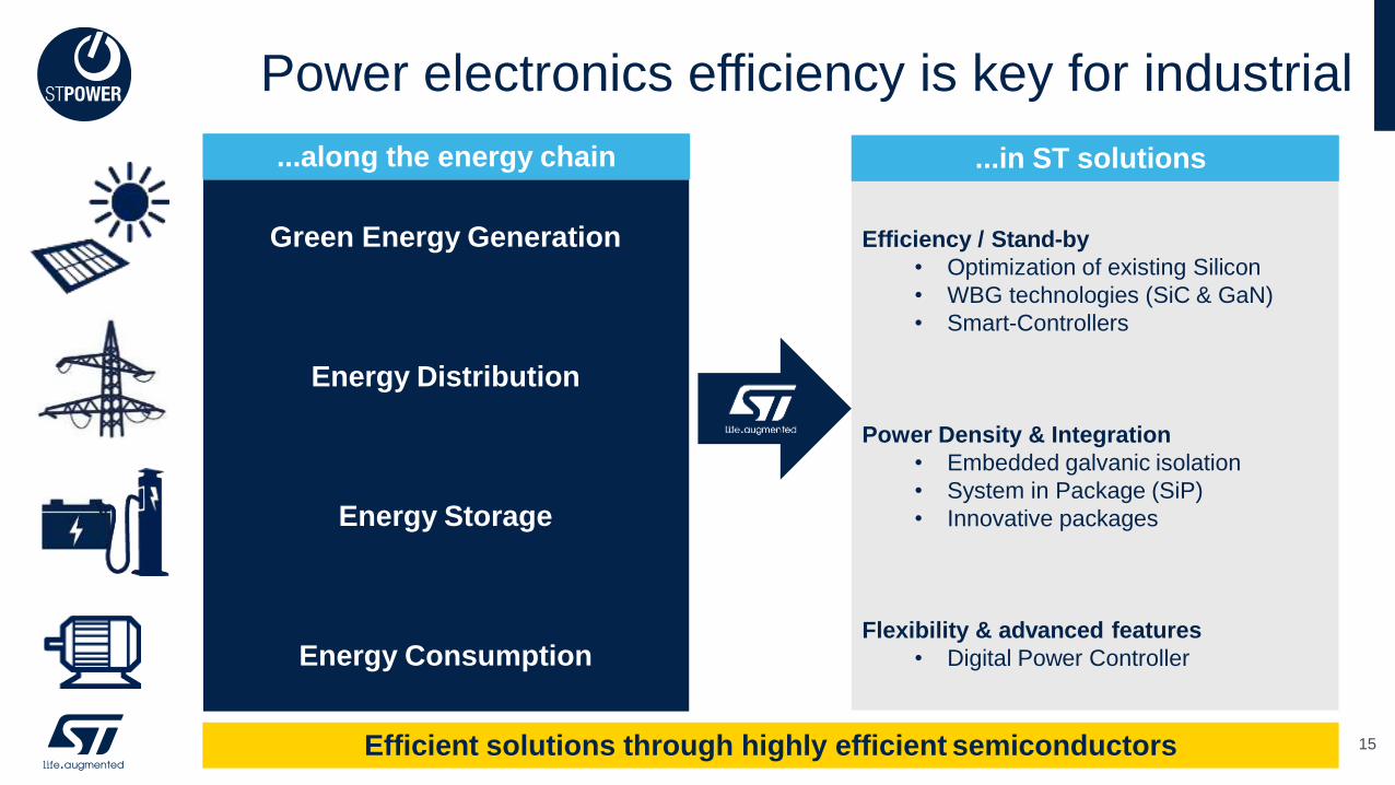
Efficiency / Stand-by
• Optimization of existing Silicon
• WBG technologies (SiC & GaN)
• Smart-Controllers
Power Density & Integration
• Embedded galvanic isolation
• System in Package (SiP)
• Innovative packages
Flexibility & advanced features
• Digital Power Controller
Green Energy Generation
Energy Distribution
Energy Storage
Energy Consumption
Efficient solutions through highly efficient semiconductors
...along the energy chain ...in ST solutions
Power electronics efficiency is key for industrial
15
Propulsion
Inverter
Electrical Power
GenerationPower Conversion
Electrical Power
Distribution
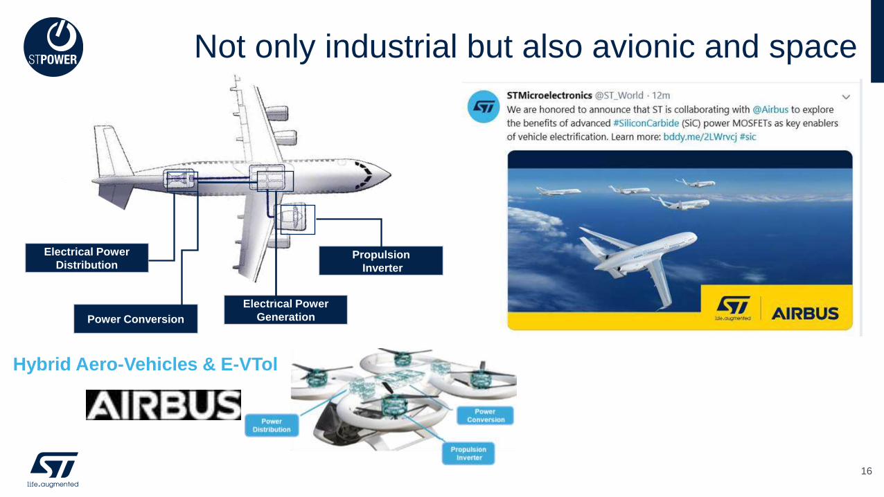
Not only industrial but also avionic and space
Hybrid Aero-Vehicles & E-VTol
16
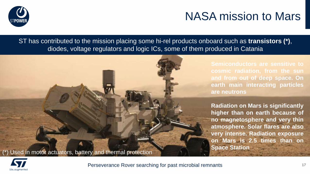
NASA mission to Mars
Perseverance Rover searching for past microbial remnants 17
Semiconductors are sensitive to
cosmic radiation, from the sun
and from out of deep space. On
earth main interacting particles
are neutrons
Radiation on Mars is significantly
higher than on earth because of
no magnetosphere and very thin
atmosphere. Solar flares are also
very intense. Radiation exposure
on Mars is 2.5 times than on
Space Station
ST has contributed to the mission placing some hi-rel products onboard such as transistors (*),
diodes, voltage regulators and logic ICs, some of them produced in Catania
(*) Used in motor actuators, battery and thermal protection
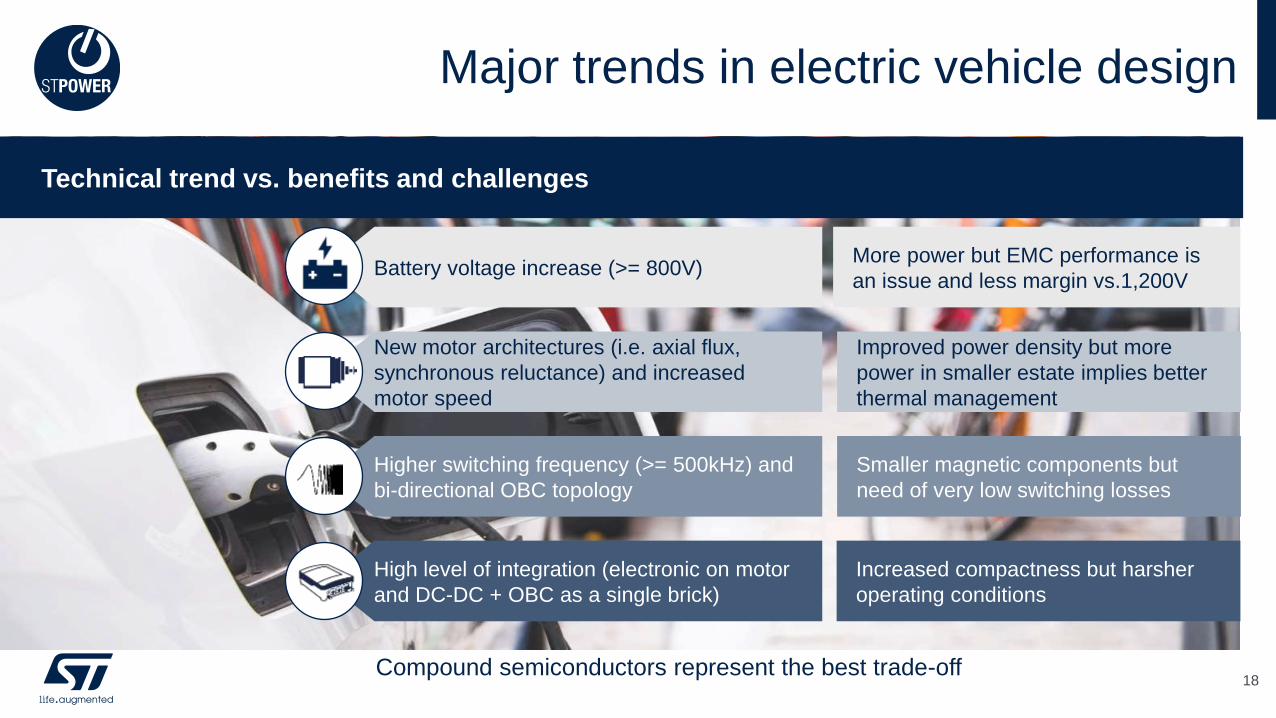
Major trends in electric vehicle design
Technical trend vs. benefits and challenges
• Battery voltage increase (>= 800V)
• New motor architectures (i.e. axial flux,
synchronous reluctance) and increased
motor speed
• Higher switching frequency (>= 500kHz) and
bi-directional OBC topology
• High level of integration (electronic on motor
and DC-DC + OBC as a single brick)
More power but EMC performance is
an issue and less margin vs.1,200V
Improved power density but more
power in smaller estate implies better
thermal management
Smaller magnetic components but
need of very low switching losses
Increased compactness but harsher
operating conditions
Compound semiconductors represent the best trade-off18
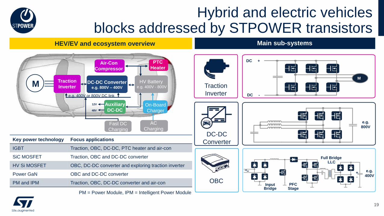
Hybrid and electric vehicles blocks addressed by STPOWER transistors
HV Battery e.g. 400V - 800VM
Traction
Inverter DC-DC Converter
e.g. 800V – 400V
On-Board
Charger
AC
Charging
Air-Con
Compressor
Auxiliary
DC-DC
12V
48V
e.g. 400V or 800V DC link
Fast DC
Charging
PTC
Heater
M
DC +
DC -
e.g.
400V+-
Input Bridge
PFC Stage
Full Bridge LLC
e.g.
800V
Key power technology Focus applications
IGBT Traction, OBC, DC-DC, PTC heater and air-con
SiC MOSFET Traction, OBC and DC-DC converter
HV Si MOSFET OBC, DC-DC converter and exploring traction inverter
Power GaN OBC and DC-DC converter
PM and IPM Traction, OBC, DC-DC converter and air-con
PM = Power Module, IPM = Intelligent Power Module
Main sub-systemsHEV/EV and ecosystem overview
DC-DC
Converter
OBC
Traction
Inverter
19
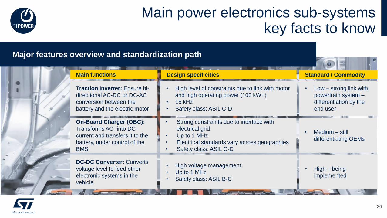
Main power electronics sub-systemskey facts to know
Major features overview and standardization path
Traction Inverter: Ensure bi-
directional AC-DC or DC-AC
conversion between the
battery and the electric motor
DC-DC Converter: Converts
voltage level to feed other
electronic systems in the
vehicle
On-Board Charger (OBC):
Transforms AC- into DC-
current and transfers it to the
battery, under control of the
BMS
• High level of constraints due to link with motor
and high operating power (100 kW+)
• 15 kHz
• Safety class: ASIL C-D
• High voltage management
• Up to 1 MHz
• Safety class: ASIL B-C
• Strong constraints due to interface with
electrical grid
• Up to 1 MHz
• Electrical standards vary across geographies
• Safety class: ASIL C-D
• Low – strong link with
powertrain system –
differentiation by the
end user
• High – being
implemented
• Medium – still
differentiating OEMs
Design specificitiesMain functions Standard / Commodity
20
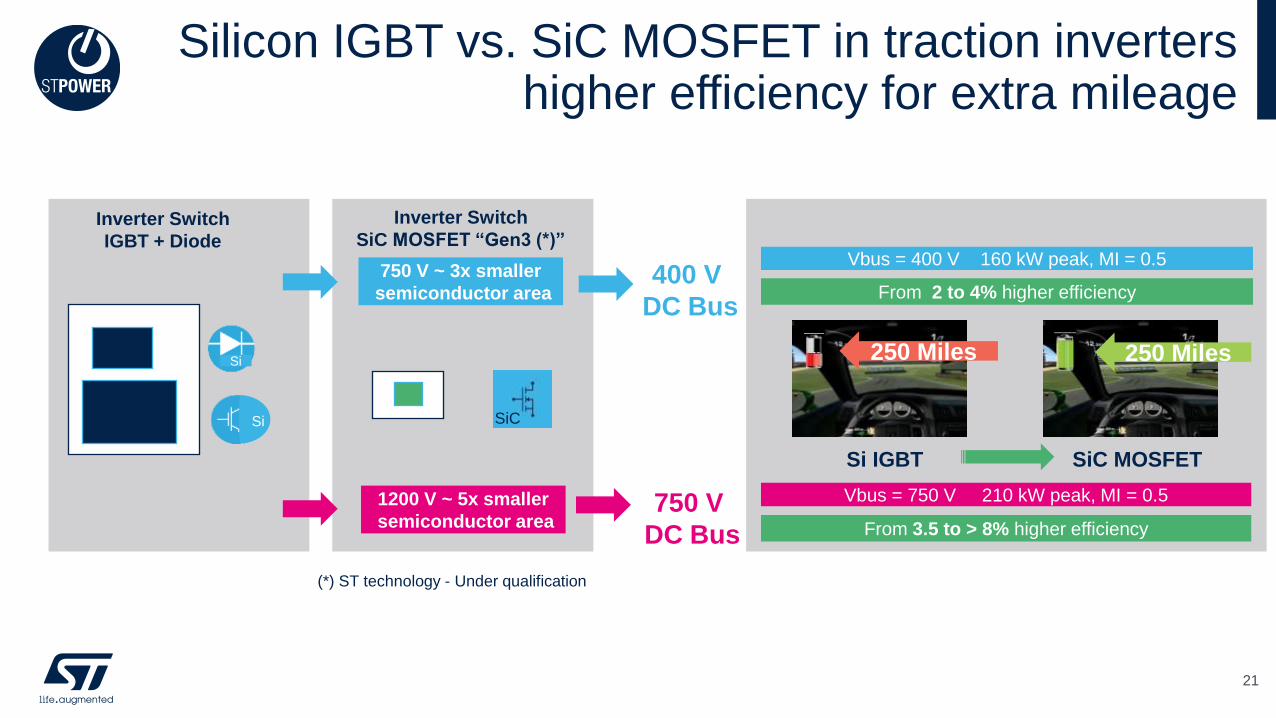
Silicon IGBT vs. SiC MOSFET in traction inverters higher efficiency for extra mileage
750 V
DC Bus
250 Miles
Si IGBT SiC MOSFET
Vbus = 400 V 160 kW peak, MI = 0.5
From 2 to 4% higher efficiency
1200 V ~ 5x smaller
semiconductor area
750 V ~ 3x smaller
semiconductor area
Vbus = 750 V 210 kW peak, MI = 0.5
From 3.5 to > 8% higher efficiency
400 V
DC Bus
Inverter Switch
SiC MOSFET “Gen3 (*)”
Si
Si
250 Miles
Inverter Switch
IGBT + Diode
(*) ST technology - Under qualification
SiC
21
4 x lower
TJ < 80% Tjmax
* Typical power losses per switch at peak power: 350 Arms
5x lower
• Topology: 210 kW three-phase inverter
• Tj < 80%*Tjmax at any condition
• 200 Arms continuous, 350 Arms peak
• POUT ≈ peak power 210 kW with MI = 0.95, Cos(phi)= 0.8
≈ 2x lower
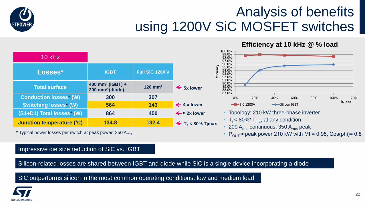
Analysis of benefits using 1200V SiC MOSFET switches
22
Losses* IGBT Full SiC 1200 V
Total surface400 mm² (IGBT) +
200 mm2 (diode)120 mm²
Conduction losses* (W) 300 307
Switching losses* (W) 564 143
(S1+D1) Total losses* (W) 864 450
Junction temperature (℃) 134.8 132.4
10 kHz
87.0%88.0%89.0%90.0%91.0%92.0%93.0%94.0%95.0%96.0%97.0%98.0%99.0%
100.0%
0% 20% 40% 60% 80% 100% 120%
Effi
cie
ncy
% loadSiC 1200V Silicon IGBT
SiC outperforms silicon in the most common operating conditions: low and medium load
Impressive die size reduction of SiC vs. IGBT
Silicon-related losses are shared between IGBT and diode while SiC is a single device incorporating a diode
Efficiency at 10 kHz @ % load
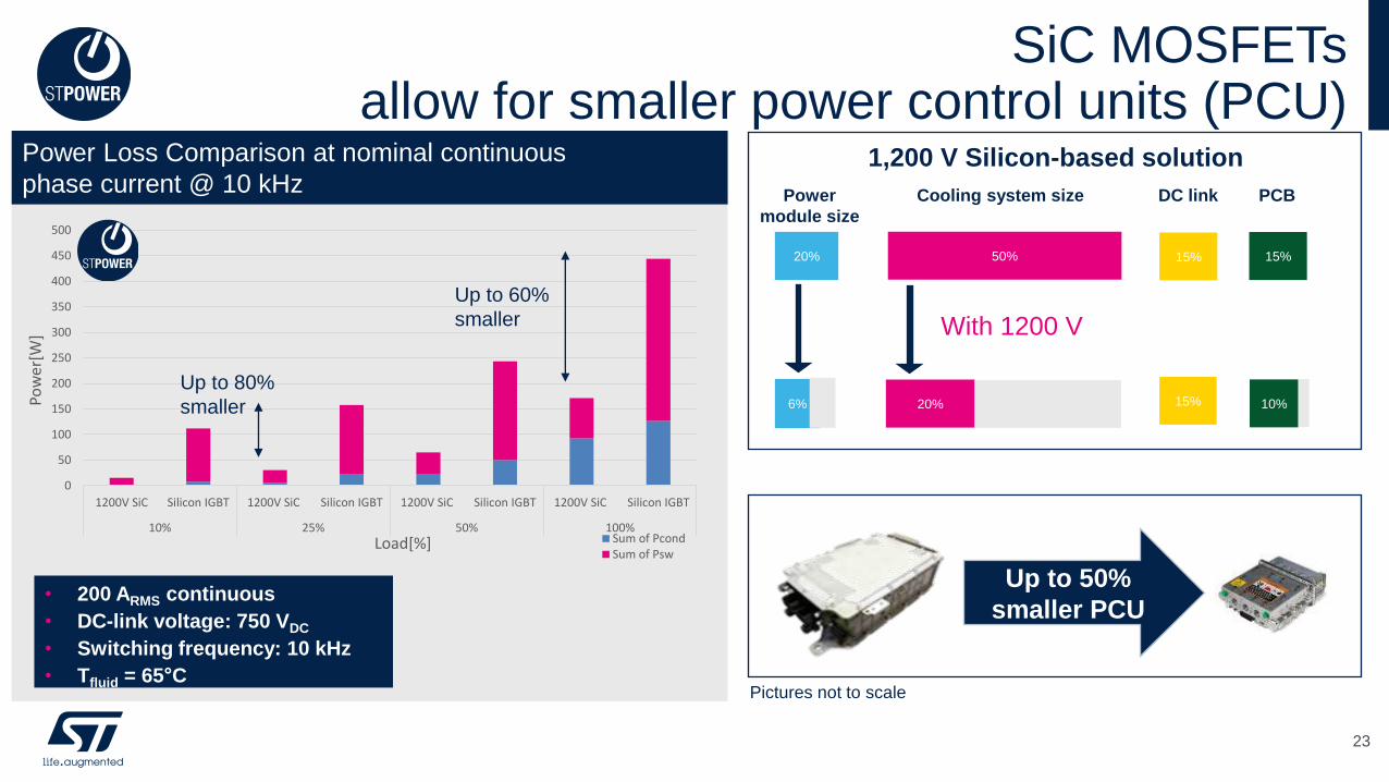
SiC MOSFETs allow for smaller power control units (PCU)
23
• 200 ARMS continuous
• DC-link voltage: 750 VDC
• Switching frequency: 10 kHz
• Tfluid = 65°C
With 1200 V
20% 50%
Power
module size
Cooling system size
15%
PCB
6% 20%
1,200 V Silicon-based solution
10%
15%
DC link
15%
0
50
100
150
200
250
300
350
400
450
500
1200V SiC Silicon IGBT 1200V SiC Silicon IGBT 1200V SiC Silicon IGBT 1200V SiC Silicon IGBT
10% 25% 50% 100%
Pow
er[W
]
Load[%] Sum of PcondSum of Psw
Up to 60%
smaller
Up to 80%
smaller
Up to 50%
smaller PCU
Pictures not to scale
Power Loss Comparison at nominal continuous
phase current @ 10 kHz
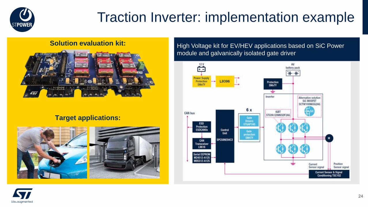
Traction Inverter: implementation example
Solution evaluation kit:
Target applications:
High Voltage kit for EV/HEV applications based on SiC Power
module and galvanically isolated gate driver
24
SiC MOSFET totem pole digital PFC with SCR
solid-state inrush current limiter
STEVAL-DPSTPFC1
Live sessions
DIPARTIMENTO di INGEGNERIA
ELETTRICA ELETTRONICA
E INFORMATICA
~
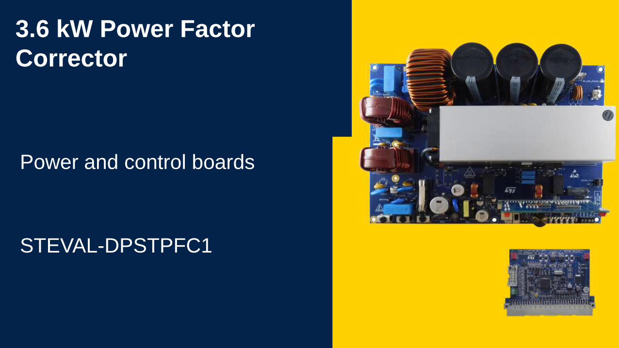
3.6 kW Power Factor
Corrector
Power and control boards
STEVAL-DPSTPFC1
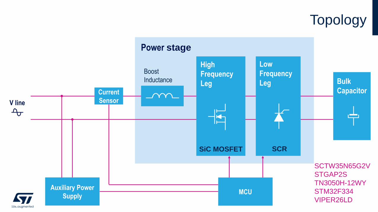
Boost
Inductance
Auxiliary Power
SupplyMCU
Power stage
Bulk
CapacitorCurrent
Sensor
SCRSiC MOSFET
High
Frequency
Leg
Low
Frequency
Leg
V line
SCTW35N65G2V
STGAP2S
TN3050H-12WY
STM32F334
VIPER26LD
Topology
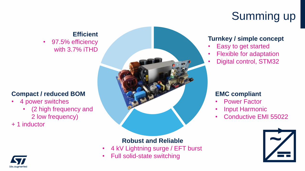
Turnkey / simple concept
• Easy to get started
• Flexible for adaptation
• Digital control, STM32
EMC compliant
• Power Factor
• Input Harmonic
• Conductive EMI 55022
Robust and Reliable
• 4 kV Lightning surge / EFT burst
• Full solid-state switching
Compact / reduced BOM
• 4 power switches
• (2 high frequency and
2 low frequency)
+ 1 inductor
Efficient
• 97.5% efficiency
with 3.7% iTHD
~
Summing up
Landing screen
Interleaved Triangular Current Mode (TCM)
Totem Pole PFC
Live sessions
DIPARTIMENTO di INGEGNERIA
ELETTRICA ELETTRONICA
E INFORMATICA

Describe theproblem solved(
more a simple picture to contextualize
speaker will have the opportunity to describe the
problem solved during the live session.
in this example, we use an image to illustrate
the risk of silent electric cars not being heard by
pedestrians)
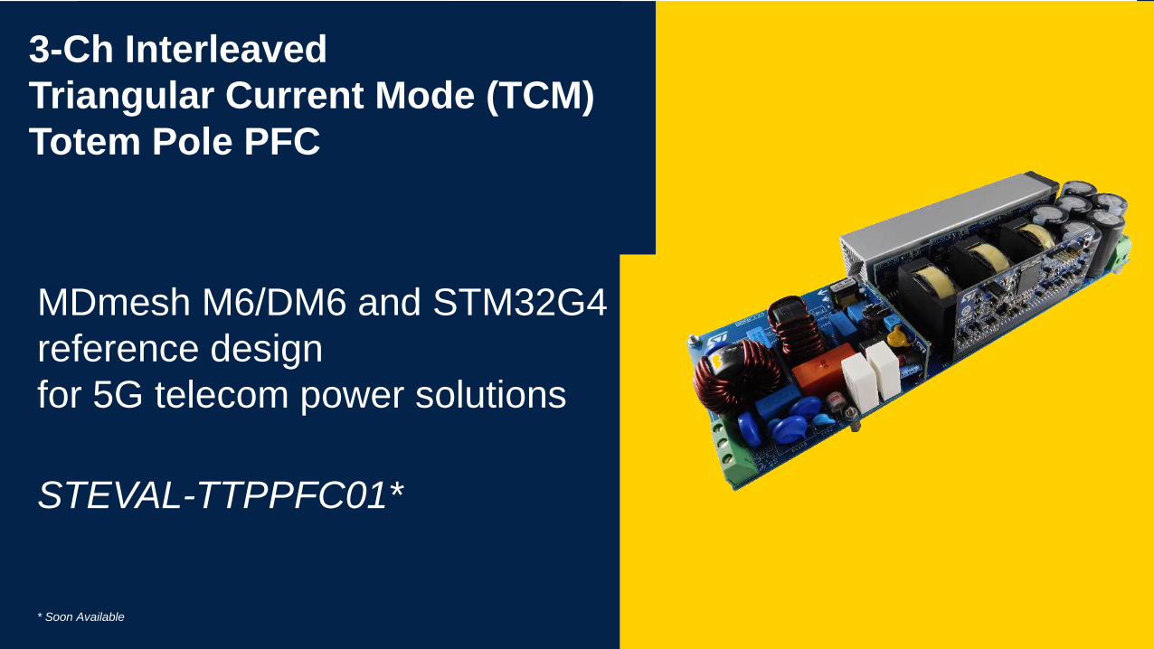
3-Ch Interleaved
Triangular Current Mode (TCM)
Totem Pole PFC
Introduce thecomponentsof your solutions(simple pictures of the board / system with a
very short
MDmesh M6/DM6 and STM32G4
reference design
for 5G telecom power solutions
STEVAL-TTPPFC01*
* Soon Available
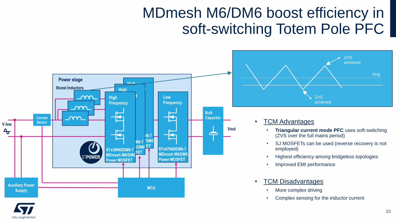
STx36N60DM6-7
MDmesh M6/DM6
Power MOSFET
High
Frequency
STx36N60DM6-7
MDmesh M6/DM6
Power MOSFET
High
Frequency
STx36N60DM6-7
MDmesh M6/DM6
Power MOSFET
High
Frequency
Boost Inductors
Power stage
Low
Frequency
STx47N60DM6-7
MDmesh M6/DM6
Power MOSFET
MDmesh M6/DM6 boost efficiency in soft-switching Totem Pole PFC
33
• TCM Advantages
• Triangular current mode PFC uses soft-switching (ZVS over the full mains period)
• SJ MOSFETs can be used (reverse recovery is not employed)
• Highest efficiency among bridgeless topologies
• Improved EMI performance
• TCM Disadvantages
• More complex driving
• Complex sensing for the inductor current
Iavg
ZVS
achieved
ZVS
achieved
Auxiliary Power
SupplyMCU
Bulk
CapacitorCurrent
SensorV line
Vout
STx36N60DM6-7
MDmesh M6/DM6
Power MOSFET
High
Frequency
STx36N60DM6-7
MDmesh M6/DM6
Power MOSFET
High
Frequency
STx36N60DM6-7
MDmesh M6/DM6
Power MOSFET
High
Frequency
Boost Inductors
Power stage
Low
Frequency
STx47N60DM6-7
MDmesh M6/DM6
Power MOSFET
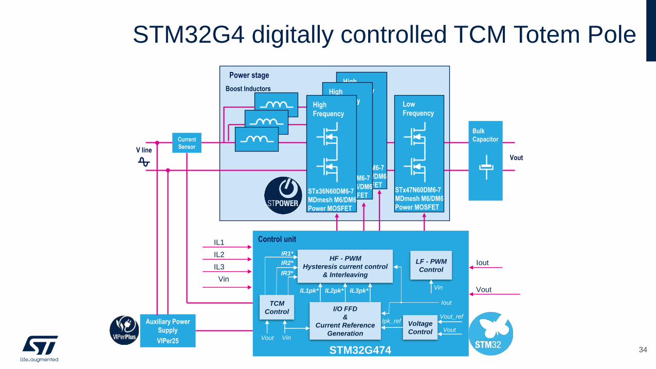
STM32G4 digitally controlled TCM Totem Pole
34
Auxiliary Power
Supply
VIPer25
Bulk
CapacitorCurrent
SensorV line
Vout
STM32G474
IR2*
Vout_ref
Voltage
ControlVinVout
Vout
Vin
Iout
HF - PWM
Hysteresis current control
& Interleaving
LF - PWM
Control
TCM
Control I/O FFD
&
Current Reference
Generation
IR3*
IL1pk*
IR1*
IL2pk* IL3pk*
Ipk_ref
IL1
Vin
IL2
IL3
Vout
Iout
STM32G474
Control unit
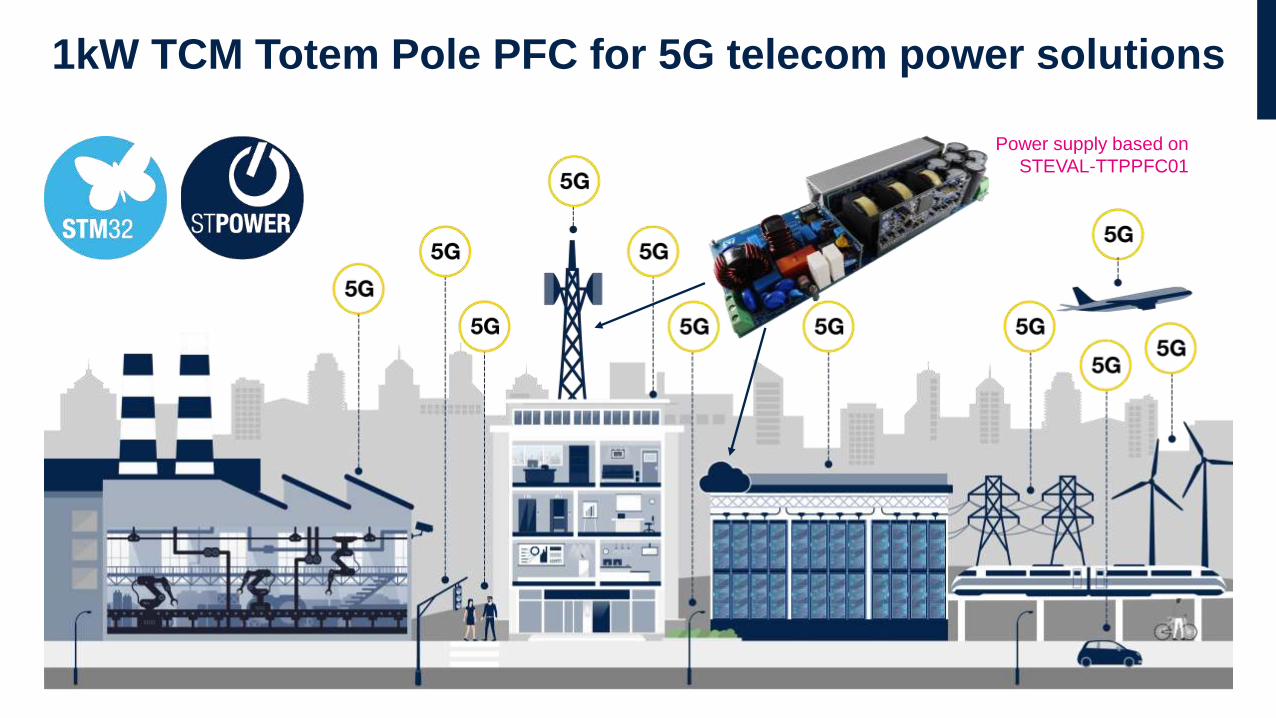
1kW TCM Totem Pole PFC for 5G telecom power solutions Wrap(Simple slide to conclude on the solution
presented)Power supply based on
STEVAL-TTPPFC01
ST overview
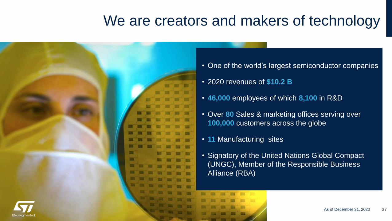
We are creators and makers of technology
• One of the world’s largest semiconductor companies
• 2020 revenues of $10.2 B
• 46,000 employees of which 8,100 in R&D
• Over 80 Sales & marketing offices serving over
100,000 customers across the globe
• 11 Manufacturing sites
• Signatory of the United Nations Global Compact
(UNGC), Member of the Responsible Business
Alliance (RBA)
As of December 31, 2020 37
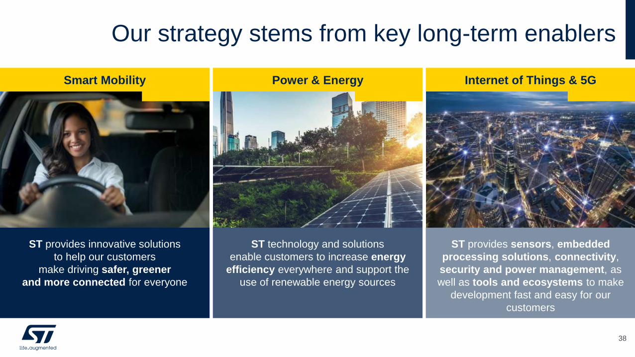
Our strategy stems from key long-term enablers
ST provides innovative solutions
to help our customers
make driving safer, greener
and more connected for everyone
Smart Mobility
ST technology and solutions
enable customers to increase energy
efficiency everywhere and support the
use of renewable energy sources
Power & Energy
ST provides sensors, embedded
processing solutions, connectivity,
security and power management, as
well as tools and ecosystems to make
development fast and easy for our
customers
Internet of Things & 5G
38
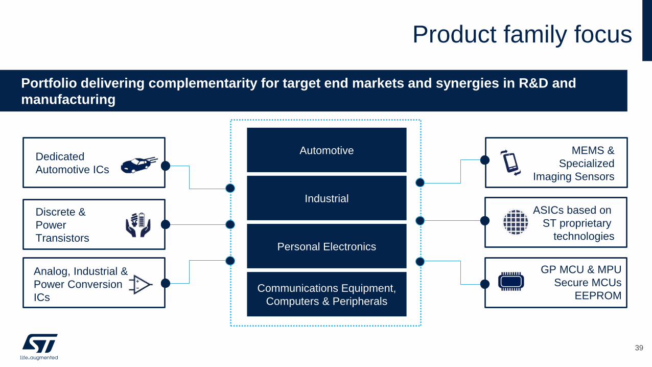
Product family focus
Portfolio delivering complementarity for target end markets and synergies in R&D and
manufacturing
Dedicated
Automotive ICs
Analog, Industrial &
Power Conversion
ICs
GP MCU & MPU
Secure MCUs
EEPROM
MEMS &
Specialized
Imaging Sensors
Discrete &
Power
Transistors
ASICs based on
ST proprietary
technologiesPersonal Electronics
Industrial
Automotive
Communications Equipment,
Computers & Peripherals
39
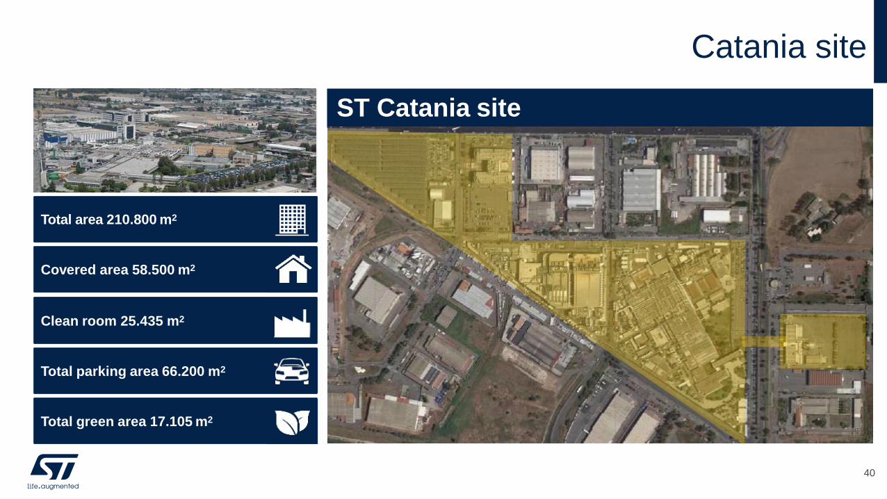
Catania site
ST Catania site
Total parking area 66.200 m2
Total green area 17.105 m2
Clean room 25.435 m2
Covered area 58.500 m2
Total area 210.800 m2
40
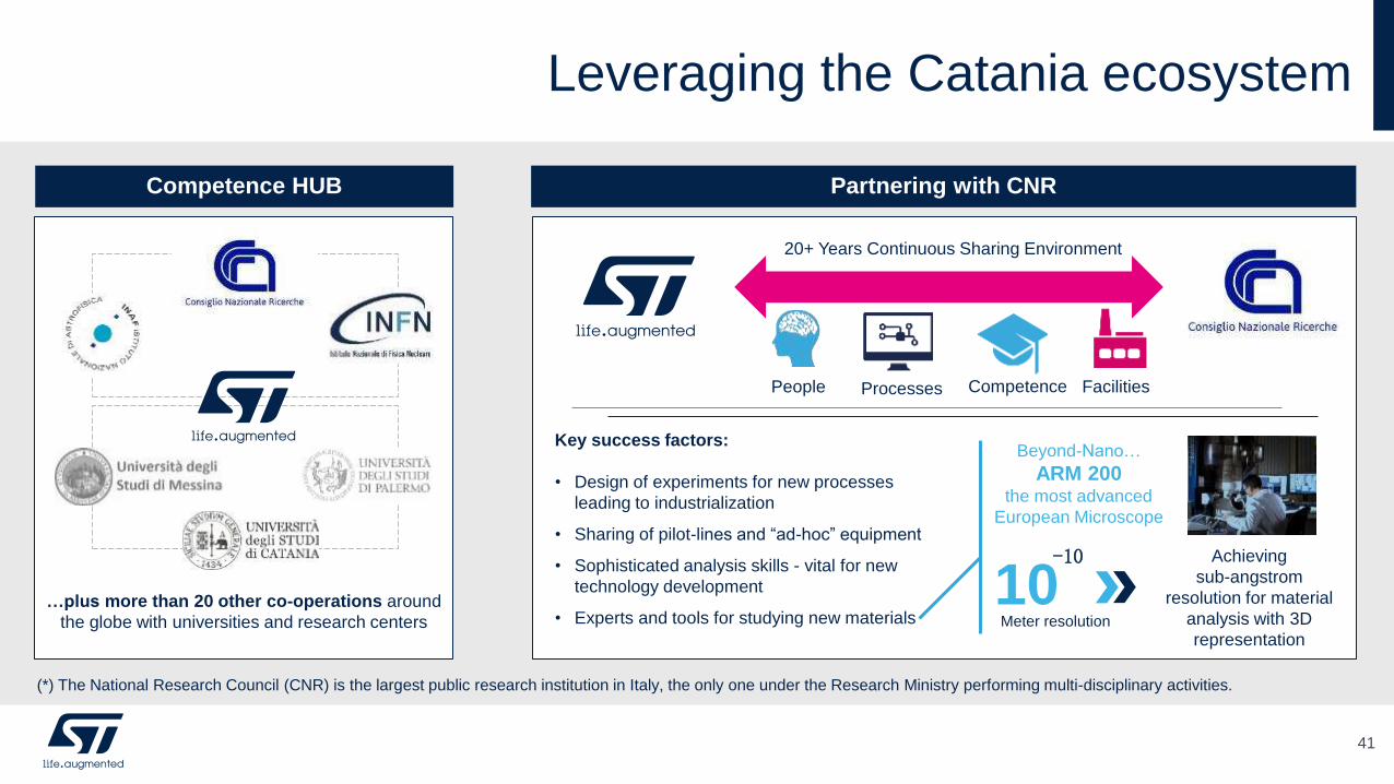
Leveraging the Catania ecosystem
Competence HUB Partnering with CNR
…plus more than 20 other co-operations around
the globe with universities and research centers
10-10
Meter resolution
People Processes Facilities
20+ Years Continuous Sharing Environment
Beyond-Nano…
ARM 200the most advanced
European Microscope
Achieving
sub-angstrom
resolution for material
analysis with 3D
representation
Competence
Key success factors:
• Design of experiments for new processes
leading to industrialization
• Sharing of pilot-lines and “ad-hoc” equipment
• Sophisticated analysis skills - vital for new
technology development
• Experts and tools for studying new materials
(*) The National Research Council (CNR) is the largest public research institution in Italy, the only one under the Research Ministry performing multi-disciplinary activities.
41
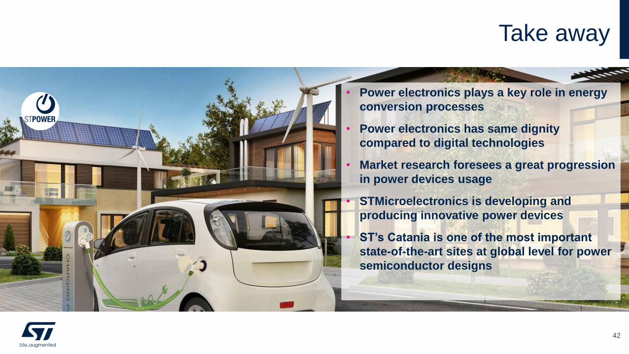
• Power electronics plays a key role in energy
conversion processes
• Power electronics has same dignity
compared to digital technologies
• Market research foresees a great progression
in power devices usage
• STMicroelectronics is developing and
producing innovative power devices
• ST’s Catania is one of the most important
state-of-the-art sites at global level for power
semiconductor designs
Take away
42
© STMicroelectronics - All rights reserved.
ST logo is a trademark or a registered trademark of STMicroelectronics International NV or its affiliates in the EU and/or other countries.
For additional information about ST trademarks, please refer to www.st.com/trademarks.
All other product or service names are the property of their respective owners.
Thank you