Embed Size (px)
Citation preview

UNIVERSITÉ DE MONTRÉAL
CONCEPTION ET RÉALISATION D’UN RÉCEPTEUR COMPOSÉ DE RÉSEAU
D’ANTENNES YAGI MULTICOUCHES VERTICALES ET DE COMPOSANTS EN ONDES
MILLIMÉTRIQUES
OLIVIER KRAMER
DÉPARTEMENT DE GÉNIE ÉLECTRIQUE
ÉCOLE POLYTECHNIQUE DE MONTRÉAL
MÉMOIRE PRÉSENTÉ EN VUE DE L'OBTENTION
DU DIPLÔME DE MAÎTRISE ÈS SCIENCES APPLIQUÉES
(GÉNIE ÉLECTRIQUE)
OCTOBRE 2010
© Olivier Kramer, 2010

UNIVERSITÉ DE MONTRÉAL
ÉCOLE POLYTECHNIQUE DE MONTRÉAL
Ce mémoire intitulé
CONCEPTION ET RÉALISATION D’UN RÉCEPTEUR COMPOSÉ DE RÉSEAU
D’ANTENNES YAGI MULTICOUCHES VERTICALES ET DE COMPOSANTS EN ONDES
MILLIMÉTRIQUES
présenté par KRAMER Olivier
en vue de l’obtention du diplôme de Maîtrise ès Sciences Appliquées
a été dûment accepté par le jury d’examen constitué de :
M. FRIGON Jean-François, Ph.D., président
M. WU Ke, Ph.D., membre et directeur de recherche
M. TATU Serioja, Ph. D., membre

iii
DÉDICACES
A ma compagne Danna, à ma famille et à mes amis.

iv
REMERCIEMENTS
Je souhaite remercier Pr. Ke Wu pour m’avoir accepté dans son équipe et guidé tout au
long de ma maitrise ainsi que pour son aide financière.
Un grand merci aussi aux professeurs du laboratoire, notamment Mr. Cevdet Akyel pour
son aide.
Je tiens aussi à remercier Mr. Jules Gautier, Mr. Steve Dubé, et Mr. Treian Antonescu
pour leurs aides et conseils concernant la fabrication des circuits.
Je voudrais finalement remercier les personnes qui travaillent au laboratoire Poly-Grames,
les étudiants, et plus précisément Mr. Tarek Djerafi et toutes les personnes avec qui j’ai partagé
mon bureau.
v
RÉSUMÉ
Les applications en ondes millimétriques telles que les réseaux sans-fils haute vitesse
demandent des composants de hautes performances, faibles coûts de revient, modulaires et
compacts. Ce mémoire présente la conception d’une chaine de démodulation en ondes
millimétriques utilisant le concept du multicouche.
Tout d’abord, une antenne Yagi multicouche est proposée et démontrée à 5.8 GHz. La
structure utilise pour la première fois les éléments parasites des antennes Yagi dans une structure
de substrats empilés verticalement. Cela permet d’atteindre un gain de 12 dBi. Deux
configuration sont présentées : une première basée sur un dipôle et une deuxième basée sur un
patch circulaire afin d’avoir une double polarisation. Les résultats mesurés montrent un très bon
accord avec les simulations.
Basé sur les principes démontrés précédemment, l’antenne est adaptée à 60 GHz, puis un
réseau d’antennes Yagi verticales en ondes millimétriques est introduit pour la première fois
exploitant les technologies multicouches. Une analyse est faite pour définir les limites du design.
L’antenne élément mesurée atteint un gain de 11 dBi. Le réseau 4x4 a une taille 50x50x60 mm3,
et atteint un gain mesuré de 18 dBi sur 7% de bande passante. Une autre configuration du réseau
utilisant des antennes Yagi inclinées permet d’avoir une réduction des lobes secondaires tout en
ayant un impact minimum sur le gain. Les antennes proposées sont d’excellents candidats pour
des systèmes intégrés, faibles coûts, demandant une petite empreinte en ondes millimétriques.
Finalement, un nouveau six-port double couche utilisant des Guides Intégrés au Substrats
(GIS) est présenté et démontré. Celui-ci permet de faire la démodulation QPSK. Son architecture
utilise des coupleurs multicouches, fournissant une grande surface de couplage à travers deux
fentes ; un déphaseur inédit, large bande composé de deux stubs plan-H et une ligne de
référence ; ainsi que de deux diviseurs de puissance. Les simulations et mesures montrent que le
circuit fonctionne correctement sur toute la bande V. La démodulation QPSK complète est testée
sous le logiciel de simulation ADS et montre les excellentes performances du système.

vi
ABSTRACT Millimeter wave applications such as high-speed wireless connections require modular,
compact-size, low-cost and high-performance systems. In order to realize a complete receiver
satisfying those requirements, compact stacked multilayered designs are presented in this thesis.
First, high-gain compact stacked multilayered Yagi designs are proposed and
demonstrated at 5.8 GHz. The structure makes use for the first time of vertically stacked Yagi-
like parasitic director elements that allow easily obtaining a simulated gain of 12 dBi. Two
different antenna configurations are presented, one based on dipole geometry for single
polarization, and the other on a circular patch to achieve dual polarization. Measured results of
the fabricated antenna prototypes are in good agreement with simulated results.
Second, based on the above-demonstrated principle, the antenna is redesigned and adapted
for 60 GHz applications, and a novel design showing for the first time an array of Yagi elements
in millimeter wave stacked structure is presented. An analysis is performed to define the structure
limits. The measured element attains 11 dBi of gain. The proposed 4x4 array has a size of
50x50x60 mm3, and reaches a measured gain of 18 dBi over 7% of bandwidth. An alternative
configuration of the array using angled Yagi antenna elements allows for a significant
improvement of the side lobe level without a visible impact on the gain. The proposed antennas
present excellent candidates for integrated low-cost millimeter-wave systems that require small
footprint.
Third, a novel dual layered six-port front-end circuit using the Substrate Integrated
Waveguide (SIW) technology is presented and demonstrated. The six-port architecture makes use
of multilayer couplers, providing a wide coupling area through two slots; a new broadband SIW
phase shifter composed of two H-plane stub lines and one reference line; and two SIW power
dividers. Simulation and measurement results show that the proposed six-port circuit can easily
operate at 60 GHz for V-band system applications. The complete QPSK demodulation is tested
through the ADS simulation platform to prove the good performances of the designed circuits.
vii
TABLE DES MATIÈRES
DÉDICACES ................................................................................................................................. III
REMERCIEMENTS ...................................................................................................................... IV
RÉSUMÉ ......................................................................................................................................... V
ABSTRACT ................................................................................................................................... VI
TABLE DES MATIÈRES ........................................................................................................... VII
LISTE DES FIGURES ................................................................................................................... IX
LISTE DES SIGLES ET ABRÉVIATIONS .................................................................................. X
LISTE DES SYMBOLES ET ABRÉVIATIONS .......................................................................... XI
INTRODUCTION ............................................................................................................................ 1
DÉMARCHE GÉNÉRALE ............................................................................................................. 6
CHAPITRE 1 ANTENNES À 5.8 GHZ ...................................................................................... 7
1.1 Théorie des antennes Yagi-Uda ....................................................................................... 7
1.2 Présentation de la réalisation ............................................................................................ 9
1.3 Article 1 - Vertically Multilayer-Stacked Yagi Antenna with Single and Dual
Polarizations ............................................................................................................................... 10
1.3.1 Introduction ................................................................................................................ 11
1.3.2 Antenna design consideration .................................................................................... 15
1.3.3 Results and Discussion ............................................................................................... 24
1.3.4 Conclusion .................................................................................................................. 29
Acknowledgment ................................................................................................................... 30
References .............................................................................................................................. 30
CHAPITRE 2 ANTENNES À 60 GHZ ..................................................................................... 33
2.1 Présentation .................................................................................................................... 33
2.2 Article 2 - Very Small Footprint 60 GHz Stacked Yagi Antenna Array ....................... 34
2.2.1 Introduction ................................................................................................................ 35
2.2.2 Stacked Yagi Antenna ................................................................................................ 37
2.2.3 4x4 stacked Yagi Antenna Array using SIW feeding Mechanism............................. 41
2.2.4 Low Side Lobe Level (SLL) 4x4 Array of stacked Yagi Antenna with slanted
elements .................................................................................................................................. 48

viii
2.2.5 Conclusion .................................................................................................................. 49
Acknowledgment ................................................................................................................... 50
References .............................................................................................................................. 50
CHAPITRE 3 DÉMODULATION ........................................................................................... 53
3.1 Choix du circuit de démodulation .................................................................................. 53
3.2 Présentation du six-port .................................................................................................. 53
3.3 Théorie du six-port ......................................................................................................... 54
3.3.1 Origine ........................................................................................................................ 54
3.3.2 Réflectométrie ............................................................................................................ 54
3.4 Jonction six-port modifiée .............................................................................................. 59
3.4.1 Présentation ................................................................................................................ 59
3.4.2 Démodulateur ............................................................................................................. 61
3.4.3 Fonctionnement en tant que discriminateur de phase ................................................ 62
3.5 Présentation de la réalisation d'une jonction six-port modifiée à 60 GHz ..................... 65
3.6 Article 3 - Dual-Layered Substrate Integrated Waveguide Six-Port with Wideband
Double Stub Phase Shifter.......................................................................................................... 66
3.6.1 Introduction ................................................................................................................ 67
3.6.2 Design Framework ..................................................................................................... 69
3.6.3 Simulated and Measured Results ............................................................................... 74
3.6.4 Conclusion .................................................................................................................. 78
Acknowledgment ................................................................................................................... 81
References .............................................................................................................................. 81
CHAPITRE 4 CIRCUIT EN BANDE DE BASE - DÉCODEUR I/Q ...................................... 83
4.1 Présentation .................................................................................................................... 83
4.2 Simulations et mesures de la jonction six-port ............................................................... 83
4.2.1 Configuration ............................................................................................................. 83
4.2.2 Résultats ..................................................................................................................... 85
CHAPITRE 5 DISCUSSION GÉNÉRALE .............................................................................. 89
CONCLUSION ET TRAVAUX FUTURS ................................................................................... 90
RÉFÉRENCES ............................................................................................................................... 93

ix
LISTE DES FIGURES
Figure 0.1 : Représentation de la chaine de réception. ..................................................................... 2
Figure 0.2 : Représentation d’un système intégré multicouche. ...................................................... 2
Figure 1.1. : Schéma de base du concept d’antenne Yagi-Uda. ....................................................... 7
Figure 1.2 : Schéma montrant le rôle du directeur dans les antennes Yagi. .................................... 8
Figure 1.3 : Gain (dB) versus Nombre d’Éléments (N). [Stutzman et Thiele (1998)] ..................... 9
Figure 3.1 : Schéma d'un réflectomètre six-port. ........................................................................... 55
Figure 3.2 : Schéma d'un six-port. ................................................................................................. 56
Figure 3.3 : Solution graphique aux équations du six-port afin de trouver Γ. ............................... 58
Figure 3.4 : Schéma montrant différents placements des points q. ................................................ 59
Figure 3.5 : Schémas des composants du six-port modifié. ........................................................... 60
Figure 3.6 : Jonction six-port modifiée classique. ......................................................................... 61
Figure 3.7 : Démodulateur utilisant une jonction six-port. ............................................................ 62
Figure 3.8 : Position des points pour θ5=π/4. ................................................................................. 64
Figure 3.9 : Modulation QPSK. ..................................................................................................... 65
Figure 4.1 : Diode Schottky. .......................................................................................................... 83
Figure 4.2 : Modélisation du détecteur de puissance. .................................................................... 84
Figure 4.3 : Circuit soustracteur à l’aide d’amplificateurs. ............................................................ 84
Figure 4.4 : Schéma de la simulation ADS de la conversion directe. ............................................ 85
Figure 4.5 : Signaux d’entrée et sortie. .......................................................................................... 86
Figure 4.6 : Spectre du signal modulé QPSK d’entrée. ................................................................. 87
Figure 4.7 : Courbes simulées et théoriques du taux d’erreur de bit pour une modulation QPSK.88

x
LISTE DES SIGLES ET ABRÉVIATIONS
ADS Advanced System Design
AGC Automatic Gain Control
BER Bit Error Rate (taux d’erreur global)
DUT Device Under Test
FPB Filtre passe bas
GIS Guide Intégré au Substrat (Cf. SIW)
HFSS High Frequency Structure Simulator
IEEE Institute of Electrical and Electronics Engineers
LNA Low-Noise Amplifier
LO Local Oscillator (Oscillateur Local)
LTCC Low Temperature Co-fired Ceramic
QPSK Quadrature Phase Shift Key
RF Radio Fréquence
S/N Signal to Noise Ratio
SIW Substrate Integrated Waveguide (Cf. GIS)
SLL Side Lobe Level
UHF Ultra High Frequency

xi
LISTE DES SYMBOLES ET ABRÉVIATIONS
λo Longueur d'onde en espace libre
µ Perméabilité magnétique
c Vitesse de la lumière dans le vide
F Fréquence
Z0 Impédance Caractéristique
Γ Coefficient de réflexion
ε Permittivité électrique
εr Permittivité relative
λ Longueur d’onde
ω Fréquence angulaire
1
INTRODUCTION
Les ondes millimétriques correspondent aux fréquences dont la longueur d’onde est de
l’ordre du millimètre, i.e. les fréquences de 30 à 300 GHz. Elles ont l’avantage d’offrir des plus
grandes largeurs de bande disponibles, des circuits plus petits ou des antennes avec un meilleur
gain. Comme exemples d’application, on peut citer les systèmes de positionnements locaux, les
systèmes de télécommunication ou encore l’imagerie (médicale ou de sécurité). Les circuits les
composant doivent être simples, à la fois robustes et fiables, ayant des coûts de fabrication faibles
et une consommation réduite.
Entre autre, l’utilisation de la plage de fréquences allant de 57 à 67 GHz dans la bande V
gagne rapidement de l’intérêt, car cette bande libérée en 2001 donne la possibilité à des transferts
de données hauts débits. Les réseaux sans-fils intérieurs de plusieurs Gb/s ou la transmission de
films haute définition non-compressés, figurent parmi les applications. La majorité des pays a
libéré cette bande et possède 5 GHz de spectre continu en commun, évitant ainsi les problèmes de
régulation entre pays. La communauté scientifique a répondu à cette récente attention en
proposant des circuits à ces fréquences [Bosco et al. (2004), Sum et al. (2009)] et en mobilisant
leurs efforts vers une standardisation internationale. Parmi celles-ci, on peut citer IEEE 802.15
Task Group 3c (TG3c) [IEEE 802.15] ou IEEE 802.11 Task Group ad (TGad) [IEEE 802.11].
Les circuits en ondes millimétriques doivent répondre aux besoins demandés par ces
applications devenant de plus en plus exigeantes. Plus spécialement, la tendance aujourd’hui est
de pouvoir combiner intégration et performance [Sun et al. (2006), Gunnarsson et al. (2005)].
L’étude faite dans ce projet de maitrise consiste en la réalisation des composants
essentiels d’une chaine de réception (front-end) fonctionnant dans la bande V. L’utilisation de
structures multicouches est privilégiée afin de démontrer la haute intégrabilité et les avantages en
termes de performance qui peuvent être atteints. L’intégration multicouche de composants coupe
avec les technologies actuelles majoritairement planaires et dont l’apport d’une nouvelle
dimension ouvre de nouvelles possibilités. L'utilisation des GIS (Guides Intégrés au Substrats ou
Substrate Integrate Waveguide en anglais) est privilégiée. Ce guide construit directement à partir
d'un substrat planaire, confine le champ électromagnétique à l’aide de deux rangées de trous
métalliques. Cette technologie permet de ne pas avoir des pertes par radiation et en conséquence
de ne pas perturber les éléments proches.
2
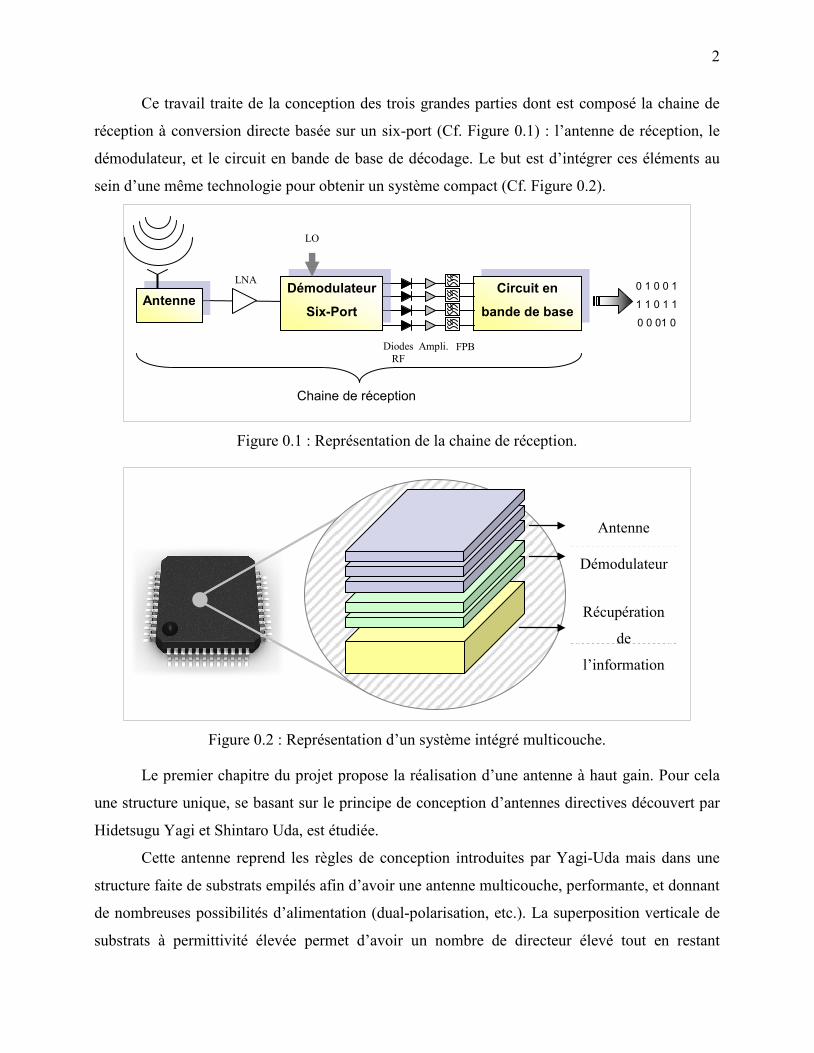
Ce travail traite de la conception des trois grandes parties dont est composé la chaine de
réception à conversion directe basée sur un six-port (Cf. Figure 0.1) : l’antenne de réception, le
démodulateur, et le circuit en bande de base de décodage. Le but est d’intégrer ces éléments au
sein d’une même technologie pour obtenir un système compact (Cf. Figure 0.2).
Figure 0.1 : Représentation de la chaine de réception.
Figure 0.2 : Représentation d’un système intégré multicouche.
Le premier chapitre du projet propose la réalisation d’une antenne à haut gain. Pour cela
une structure unique, se basant sur le principe de conception d’antennes directives découvert par
Hidetsugu Yagi et Shintaro Uda, est étudiée.
Cette antenne reprend les règles de conception introduites par Yagi-Uda mais dans une
structure faite de substrats empilés afin d’avoir une antenne multicouche, performante, et donnant
de nombreuses possibilités d’alimentation (dual-polarisation, etc.). La superposition verticale de
substrats à permittivité élevée permet d’avoir un nombre de directeur élevé tout en restant
Antenne
Démodulateur
Récupération
de
l’information
Circuit en
bande de base
Chaine de réception
0 1 0 0 1
1 1 0 1 1
0 0 01 0
Diodes RF
Ampli. FPB
Antenne LNA
Démodulateur
Six-Port
LO

3
compact, et donc avoir un gain important comparé aux antennes Yagi microstrip planaires à
même nombre d’éléments. Afin de faciliter la phase de conception, deux premiers designs sont
étudiés à 5.8 GHz vérifiant le fonctionnement du principe introduit, mais sans les contraintes de
fabrication, de mesures (analyseur réseau et chambre anéchoïque) présentes à 60 GHz. Ces deux
designs ont été réalisés : un premier basé sur un dipôle imprimé sur substrat ; un deuxième basé
sur une antenne patch circulaire permettant des polarisations orthogonales. Une étude
approfondie des paramètres critiques à la conception a été faite, comme sur la taille du plan de
masse (réflecteur).
Le deuxième chapitre se base sur les bons résultats obtenus précédemment pour concevoir
une structure fonctionnant à 60 GHz. Étant donné que l’espacement entre les éléments de
l’antenne Yagi est inversement proportionnel à la fréquence, cette structure devient très attractive
à hautes fréquences car elle devient exceptionnellement compacte et les espaces d’air requis entre
les couches à basses fréquences (comme à 5.8 GHz) disparaissent. Cet élément fonctionnant à 60
GHz est ensuite repris pour être adapté en un réseau 4x4 d’antennes Yagi réalisé en utilisant la
technologie des GIS. L’antenne créée atteint un gain de 19 dBi avec une empreinte minimale (un
réseau planaire classique de même gain est quatre fois plus étendu en surface). En ajoutant plus
d’éléments, un gain très élevé peut être réalisé tout en ayant une bonne efficacité, ce qui en fait
un candidat parfait pour les systèmes d’imagerie. Le réseau possède de plus la possibilité
d’orienter chaque élément qui le compose. Cela permet de pouvoir manipuler la forme du
faisceau d’antenne (en réduisant par exemple les lobes secondaires, avoir une meilleure largeur
de faisceau, etc.) ou de pouvoir augmenter la bande passante. Une antenne utilisant ce dernier
principe et minimisant le niveau des lobes secondaires a été conçue et mesurée.
Le troisième chapitre consiste en un système de démodulation compact, performant et
multicouche. Par rapport aux récepteurs hétérodynes conventionnels, les récepteurs à conversion
directe permettent la réduction de la complexité du circuit, un niveau élevé d’intégration et une
réduction du taux d’erreur de bit en diminuant les imperfections de fabrication. Pour ces raisons,
un démodulateur six-port passif utilisant la technologie des GIS a été choisi. Cette plateforme
développée pour la première fois permet de tirer avantage de la large surface de couplage planaire
des coupleurs et utilise un déphaseur inédit, large bande, basé sur des stubs plan-H. Ce déphaseur
a été modélisé mathématiquement, simulé et réalisé. Le six-port complet réalisé montre
d’excellentes performances en phase et en amplitude sur toute la bande allant de 55 à 65 GHz.

4
Le quatrième chapitre étudie le circuit en bande de base du démodulateur permettant la
récupération de l’information. Les performances du système de démodulation couplé avec le six-
port sont étudiées.
Finalement, ce travail est conclu en mettant en avant les nouveaux concepts présentés et
leurs possibles évolutions.
Ce mémoire montre les résultats qui peuvent être atteints en technologie multicouche et
analyse les phénomènes mis en jeux. Ces résultats peuvent facilement être réalisés avec les
nouveaux processus comme le LTCC ou la technologie film-épais photosensible permettant ainsi
d’atteindre des fréquences plus élevées et d’automatiser la conception. Les principales
contributions originales apportées par ce mémoire sont :
• Une nouvelle topologie d'antenne Yagi à substrats empilés a été proposée. Le
fonctionnement et les propriétés de ces antennes ont été montrés à 5.8 GHz (pour des
applications de plateformes de positionnement local, de systèmes de capteurs sans fils et de
radars) et en fréquences millimétriques. Elles permettent la création d’antennes passives à
haut gain ayant une grande flexibilité d’alimentation (e.g. dual-polarisation). Une méthode
de conception systématique et les limitations de cette structure sont présentées.
• L’antenne Yagi élément a été adaptée avec succès dans un réseau d’antenne fonctionnant à
60 GHz. Cette structure est attrayante car elle apporte les avantages des réseaux à celle-ci.
Ces antennes ont la possibilité d’atteindre un gain très élevé. Elles sont peu couteuses, ont
une empreinte plus petite que les antennes actives utilisées actuellement en hautes fréquences
et les systèmes basés sur celles-ci consomment moins. Cela en fait une plateforme idéale
pour les domaines de l’imagerie millimétrique ou térahertz (de sécurité, médicale ou pour
l’aéronautique).
• L’utilisation de différentes orientations d’antennes au sein du réseau (utilisant les propriétés
des antennes Yagi) a permis de modifier le diagramme de rayonnement pour réduire le
niveau des lobes secondaires. Cette caractéristique peut permettre de résoudre les problèmes
de trajets multiples (en plaçant des zéros sur le diagramme de rayonnement), d’augmenter
l’angle de balayage électrique d’un réseau ou d’adapter le rayonnement de l’antenne à
chaque application.
• Un six-port double couche a été conçu, fabriqué et mesuré. Sa topologie est étudiée afin qu’il
possède six accès exactement contrairement aux configurations classiques à huit accès
5
(nécessitant leur adaptation). Son comportement, son fonctionnement et son efficacité ont été
simulés dans le système global.
• Une étude exhaustive du nouveau déphaseur contenu dans le six-port a été faite, avec un
modèle prédisant les résultats de simulations et de mesures.
• L’intégration en GIS du réseau d’antenne et du six-port permet d'obtenir une excellente
isolation entre les éléments du canal réception, évitant les problèmes d’interférences.
Ce mémoire est présenté par article et reprend trois articles dont je suis l’auteur et le
contributeur principal: un publié dans IEEE Transaction on Antennas & Propagation et deux
soumis respectivement dans IEEE Transaction on Antennas & Propagation et IEEE MTT-S
Transaction. Il est aussi à noter que les antennes présentées ici ont été reprises par des doctorants
afin de les adapter à plus hautes fréquences et qu’un processus de valorisation est entrepris avec
l’École Polytechnique de Montréal et Univalor afin d’explorer leur potentiel.
6
DÉMARCHE GÉNÉRALE
Ce mémoire présente trois articles intégrés dans le corps du travail. Le premier article
intitulé “Vertically Multilayer-Stacked Yagi Antenna with Single and Dual Polarizations” a été
publié dans IEEE Transaction on Antennas & Propagation en avril 2010. L’article intitulé “Very
Small Footprint 60 GHz Stacked Yagi Antenna Array” a été soumis dans IEEE Transaction on
Antennas & Propagation le 25 novembre 2010 et l’article “Dual-Layered Substrate Integrated
Waveguide Six-Port with Wideband Double Stub Phase Shifter” dans IEEE MTT-S Transaction
le 25 novembre 2010. Ces revues ont été choisies car elles sont reconnues mondialement et font
office de référence dans le domaine des antennes et des circuits passifs micro-ondes. La rédaction
des articles a fait l’objet d’un soin poussé afin de répondre aux contraintes de rigueur et d’analyse
demandées par les revues prestigieuses et par ce mémoire de maitrise. La rédaction des articles
est condensée afin de respecter les normes d’espace et de mise en page, imposées par les
publications. Chaque chapitre se concentre sur une étape de conception du système. Avant
chaque article, une présentation est faite afin de donner le contexte de l’article, les informations
théoriques nécessaires à sa compréhension ainsi que la littérature pertinente. Les articles sont
insérés au fil de la démarche de travail permettant d’aider à la compréhension.
Les trois articles ont comme auteurs : moi-même, Tarek Djerafi et Ke Wu. Les
simulations, le développement, l’envoi en fabrication, les mesures, les expérimentations et la
rédaction des articles a été faite par moi. Tarek Djerafi et Ke Wu m’ont conseillé et m’ont
apporté leur expérience tout au long des travaux. Ils m’ont aussi aidé concernant les standards de
rédaction d’articles IEEE. Le pourcentage de ma contribution réelle par rapport à celles des autres
coauteurs est d’environ 75%.

7
CHAPITRE 1 ANTENNES À 5.8 GHZ
1.1 Théorie des antennes Yagi-Uda
Ayant besoin d’une antenne avec un gain relativement élevé, l’antenne de type Yagi-Uda
se révèle être un excellent candidat pour l’antenne de réception de notre système [Yagi (1928),
Uda (1930)]. L’antenne de Yagi est devenue très populaire en raison de sa simplicité et de son
gain élevé réglable (une antenne Yagi de trois éléments peut atteindre un gain de 9dB une fois
optimisée). Une antenne de Yagi-Uda de trois éléments se compose d'un dipôle (aussi appelé
conducteur/driver) de longueur λ/2, soutenu par un réflecteur légèrement plus long et un directeur
de l'autre côté (Cf. Figure 1.1.). L’application générale la plus connue de l’antenne Yagi-Uda est
l’antenne de télévision UHF.
Figure 1.1. : Schéma de base du concept d’antenne Yagi-Uda.
Dans ce type d’antenne, seul le dipôle est alimenté. L’élément réflecteur, comme son nom
l’indique, réfléchit les champs afin d’augmenter le gain dans la direction voulue.
Les directeurs auront un courant induit par l’émission du dipôle et émettront à leurs tours. Leur
position doit être soigneusement choisie pour que l’ensemble des champs rayonnés par les
éléments de l’antenne, s’additionne dans la direction voulue et s’annule dans la direction
opposée. La Figure 1.2 [Wikipedia.fr] représente ce qui se passe avec une antenne constituée
d’un dipôle et d’un directeur, ainsi que l’amplitude du champ. Le directeur est placé à une
distance de λ/10 (36° de déphasage) du dipôle. Le retard de phase de courant du directeur peut
être ajusté en modifiant sa longueur. Cette longueur est définie pour que l’onde arrière soit en
Réflecteur Dipôle Directeur
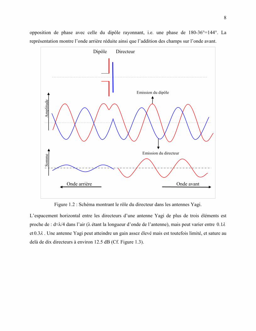
8
opposition de phase avec celle du dipôle rayonnant, i.e. une phase de 180-36°=144°. La
représentation montre l’onde arrière réduite ainsi que l’addition des champs sur l’onde avant.
Figure 1.2 : Schéma montrant le rôle du directeur dans les antennes Yagi.
L’espacement horizontal entre les directeurs d’une antenne Yagi de plus de trois éléments est
proche de : d≈λ/4 dans l’air (λ étant la longueur d’onde de l’antenne), mais peut varier entre λ1.0
et λ3.0 . Une antenne Yagi peut atteindre un gain assez élevé mais est toutefois limité, et sature au
delà de dix directeurs à environ 12.5 dB (Cf. Figure 1.3).
Dipôle
Onde avant Onde arrière
Som
me
Am
plitu
de
Emission du dipôle
Emission du directeur
Directeur

9
Figure 1.3 : Gain (dB) versus Nombre d’Éléments (N). [Stutzman et Thiele (1998)]
1.2 Présentation de la réalisation
L’idée générale est de pouvoir fabriquer une antenne Yagi-Uda multicouche (plusieurs
couches empilées) afin de garder les performances et avantages d’une telle structure tout en ayant
une configuration compacte et intégrable. Dans la cadre de ce travail, une première étude a été
faite sur ce type d’antenne à 5.8 GHz. Cela a permis de définir les règles de design, les
caractéristiques d’une telle antenne, les paramètres critiques et d’étudier la structure à une
fréquence de travail plus aisée qu’en ondes millimétriques.
10
1.3 Article 1 - Vertically Multilayer-Stacked Yagi Antenna with
Single and Dual Polarizations
Olivier KRAMER, Tarek DJERAFI, and Ke WU, Fellow, IEEE
“Vertically Multilayer-Stacked Yagi Antenna with Single and Dual Polarizations”
Publié dans “IEEE Transactions on Antennas and Propagation” en Avril 2010, dans le Volume:
58 Issue:4, pages: 1022 - 1030
11
Abstract— There are many applications such as local positioning systems (LPS) and
wireless sensor networks that require high-directivity and compact-size antennas. The
classical Yagi-Uda antenna may be useful in meeting such demands, which however,
becomes very large in size to achieve a high-gain performance due to a large number of
directors as well as space required between those elements. In this paper, high-gain yet
compact stacked multilayered Yagi antennas are proposed and demonstrated at 5.8 GHz
for LPS applications. This structure makes use of vertically stacked Yagi-like parasitic
director elements that allow easily obtaining a simulated gain of 12 dB. Two different
antenna configurations are presented, one based on dipole geometry for single polarization,
and the other on a circular patch to achieve dual polarization. The characteristics of these
antennas with respect to various geometrical parameters are studied in order to obtain the
desired performance. Measured results of the fabricated antenna prototypes are in good
agreement with simulated results. The measured dipole Yagi antenna attains 11 dB gain
over 14% bandwidth with a size of 80x80x29mm3. Radiation patterns of the dual-polarized
Yagi antenna are nearly identical to those of the single-polarized antenna, which has a size
of 50x50x60mm3, and also its two-port isolation is found to be as low as -25 dB over 4%
bandwidth. The proposed antennas present an excellent candidate for compact and low-cost
microwave and millimeter-wave integrated systems that require fixed or variable
polarization capabilities and small surface footprint.
Index Terms—Microstrip antenna, Yagi-Uda, stacked antenna, dipole, circular patch,
balun, dual polarization.
1.3.1 Introduction
he Local Positioning System (LPS) is a radio system used to search for and track down in
real time objects of interest within a limited space range. This is a typical application of
wireless sensor networks. With the LPS, a mobile object can be localized and can also collect
information about its position at a precise time instant [1]. Applications of such a LPS system are
multiple and diverse. Those systems are used for zone security with great efficiency, particularly
indoor applications such as at airports where security is mandatory. Also location tracking can
T
12
clearly improve maneuver of the business and logistics management, for example, hospitals can
improve their healthcare services by keeping a constant track of the location of doctors, nurses,
etc. LPS can also be used in many other applications such as construction and agriculture, leisure
and sports, etc. For a full integration with GPS systems that are usually used for outdoor
scenarios, LPS is expected to achieve the challenging task of being accurate, low-cost and
autonomous at ISM frequencies such as 5.8 GHz. Therefore, compact, light and low-cost antenna
is required for such LPS design and implementation.
The Yagi antenna, which has been very popular because of its simplicity as well as its
customizable high gain (three-element Yagi antenna can reach 9 dB when optimized) [2], can be
used for this type of applications. The basic unit of a three-element Yagi antenna consists of a
half-wavelength driver dipole backed by a longer reflector and a director on the other side.
Several microstrip-based Yagi or quasi-Yagi antenna structures have been reported in the
literature [2]-[8]. Interesting approaches are related to the design of a microstrip Yagi array based
on the microstrip patch antenna such as the array developed in [3] for mobile satellite system in
the L-band. The antenna developed was based on patches, consisting of one reflector, one driving
element and two directors. An array of four antenna elements was successfully used to achieve
the required performance. The design reported in [4] was made on the basis of patches instead of
dipoles as the driver element. An interesting printed Yagi antenna configuration was presented in
[5], [6] where the Yagi-like printed dipole array antenna was fed by a microstrip-to-coplanar strip
transition. In this case, a truncated microstrip ground plane was utilized as a reflecting element.
On the other hand, an active quasi-Yagi version was proposed [7] for 5.8 and 60 GHz
applications. In [8], the proposed antenna consisted of a dipole as a driving element, a
parasitically coupled reflector and six directors. The antenna was designed by utilizing the same
design rules as used in the conventional Yagi dipole antenna while taking into account the fact
that the antenna was made on a planar substrate. The antenna was designed for 5 GHz band and
has achieved a gain of 10dB.
To overcome the problem of size and footprint within the planar structure, two novel high-gain
compact structures based on the Yagi-Uda antenna concept are presented for the first time in this
work. These structures are constructed in a multilayer topology by stacking together the reflector,
the driver, and the directors. Compared to the above-described uniplanar Yagi antennas, this
design is able to provide a number of advantages. First of all, the usage of the third dimension

13
(the vertical dimension) that has not been widely used in the design of microstrip antennas,
allows an effective reduction in size and footprint. In fact, multilayer processing techniques have
become more mature in integrated circuit design, fabrication and integration. Second, a high
permittivity substrate can be used in this case, thereby reducing spacing between the directors,
which is critical for a high-density integration between antenna and circuits. Third, the possibility
of a dual polarization design based on the Yagi antenna concept is made possible, and the
coupling-based feed mechanism can achieve wide bandwidth characteristics.
Various stacked structures were investigated as in [9] and [10]. The advantage of those
topologies is that substrate thickness can be adjusted to achieve an optimized bandwidth
performance. Unlike the Yagi antenna, which is a traveling-wave antenna [11], the structure is a
resonant mode antenna. In the Yagi structure, the director is smaller than the driver and the
distance between them is between 0.2λ and 0.45λ. In [9] the thickness of the used substrate is
about 0.015λ, the bandwidth is 70 % wider than the single patch without gain improvement and
the upper layer patch is bigger. Li studied theoretically different patch shapes (square, circular,
triangle, etc.) and investigated the optimal combination to achieve a lower cross polarization or
circular polarization [10]. The substrate to wavelength in the dielectric ratio is close to 0.02.
Stacked triangular microstrip antennas were also investigated experimentally in [12] to achieve a
bandwidth about 17-5% at the centre frequency of 3.407 GHz.
To demonstrate the proposed concepts and design features, we will present two case studies in
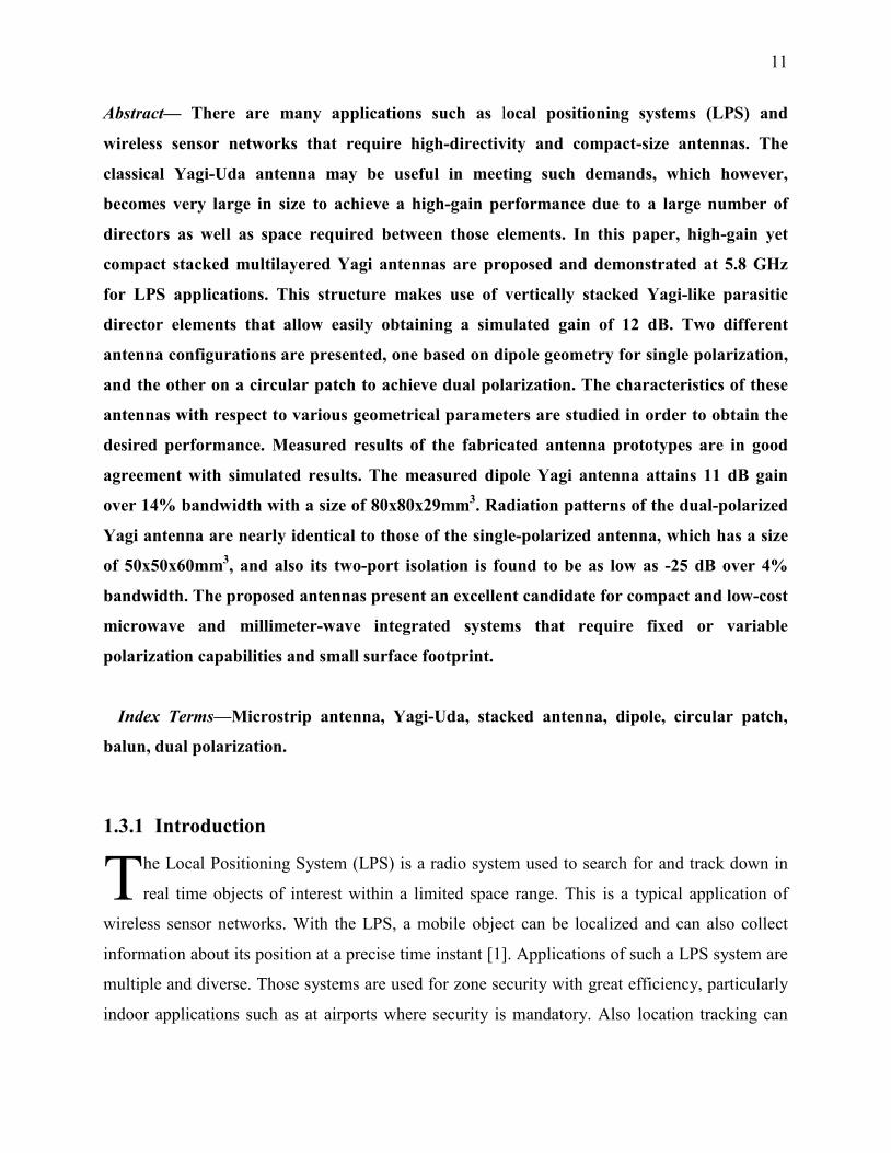
connection with the design of respective structure. The first design (see Fig. 1) is a multilayered
printed-circuit version of the proposed Yagi antenna. It consists of a ground plane (as a reflector),
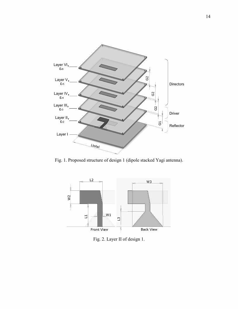
a dipole (as a driver), and four directors. In the second design (see Fig. 3), the antenna presents a
dual polarization using circular patches in the design of one driver element and four directors.
14
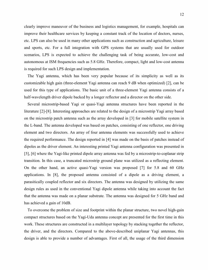
Fig. 1. Proposed structure of design 1 (dipole stacked Yagi antenna).
Fig. 2. Layer II of design 1.
15
Fig. 3. Proposed structure of design 2 (dual polarization circular patches).
In this paper, the configuration of the proposed Yagi-Uda antenna is described in detail. Design
specifications are discussed, considering the effects of different dimensions on antenna
performances. Both proposed antennas as described in Fig. 1 and Fig. 3 are fabricated. Simulated
and measured results are then compared, and the work is finally concluded.
1.3.2 Antenna design consideration
1.3.2.1 Dipole Stacked Yagi Antenna (Design #1)
The configuration of the dipole stacked Yagi antenna shown in Fig. 1, is based on the classical
Yagi-antenna design principle. It consists of one dipole driver element, and four parasitic
elements. The antenna is designed on the basis of the same design rules that are used in the
conventional Yagi dipole antenna, except that the antenna is made on a planar substrate.
There have been many different design versions for printed dipole antennas and baluns, as well
as coplanar strip dipoles fed by coplanar waveguide and stripline balun used to feed a printed
quasi-Yagi antenna proposed in [5]. The proposed dipole allows the avoidance of a balun which
becomes usually necessary when dipole antennas are fed by an unbalanced line. The dipole (layer
II in Fig. 1) is printed on both sides of a dielectric substrate [13], [14], [15]. The bottom-tapered
16
ground transition is designed to provide an impedance matching tuner with balanced output. The
designed feed network of the dipole antenna with the tapered balun transition is tuned by the
angle of the tapered ground plane for impedance matching and balanced output. This simplified
feeding structure results in the reduction of transmission line length and in turn radiation loss.
Moreover, it has attractive wide bandwidth capabilities. The feeding dipole bandwidth (without
any Yagi antenna elements) is relatively large; a bandwidth of 29% can be achieved at 5.8GHz
using a 30 mil thick substrate with a relative permittivity of 2.33 (Rogers RT/Duroïd5870).
Director elements fabricated on substrates having a relative permittivity of 3.48 results in
significantly reduced spacing between them. In the Yagi-antenna design, the gap between the
elements is approximately given by
0 14
≈ ⋅r
dλ
ε (1)
where εr is the relative dielectric constant of the substrate (the constant of air in the classical
Yagi-Uda antenna design) and 0λ is the free space wavelength. This equation clearly shows that
if the dielectric constant is increased, the gap is reduced. In this design, the substrates should be
stacked ideally without any air gaps. However, the layers are still very thick at 5.8GHz, which are
not feasible and affordable for fabrication. Of course, this is no longer a problem at very high
frequencies such as millimeter-wave ranges.
Antenna characteristics such as gain, front-to-back ratio, beamwidth and center frequency can
be altered by changing the length of the driven element, the length of the parasitic elements, the
spacing between reflector and dipole, the spacing between director and dipole, the spacing
between directors or substrate thickness as well as the dielectric constant. It is shown that an
array configuration is completely determined when any two of these constraints are specified
[16]. The proposed stacked dipole Yagi antenna is simulated by using Ansoft Designer v2.0, a
commercial simulator that can solve electric and magnetic fields via a method of moment.
17
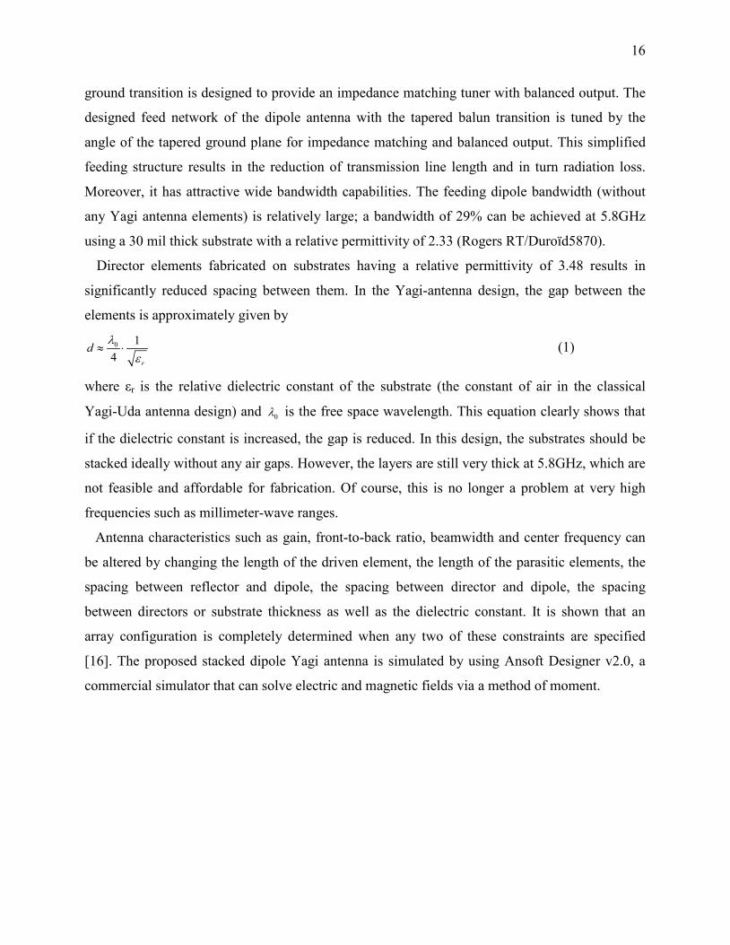
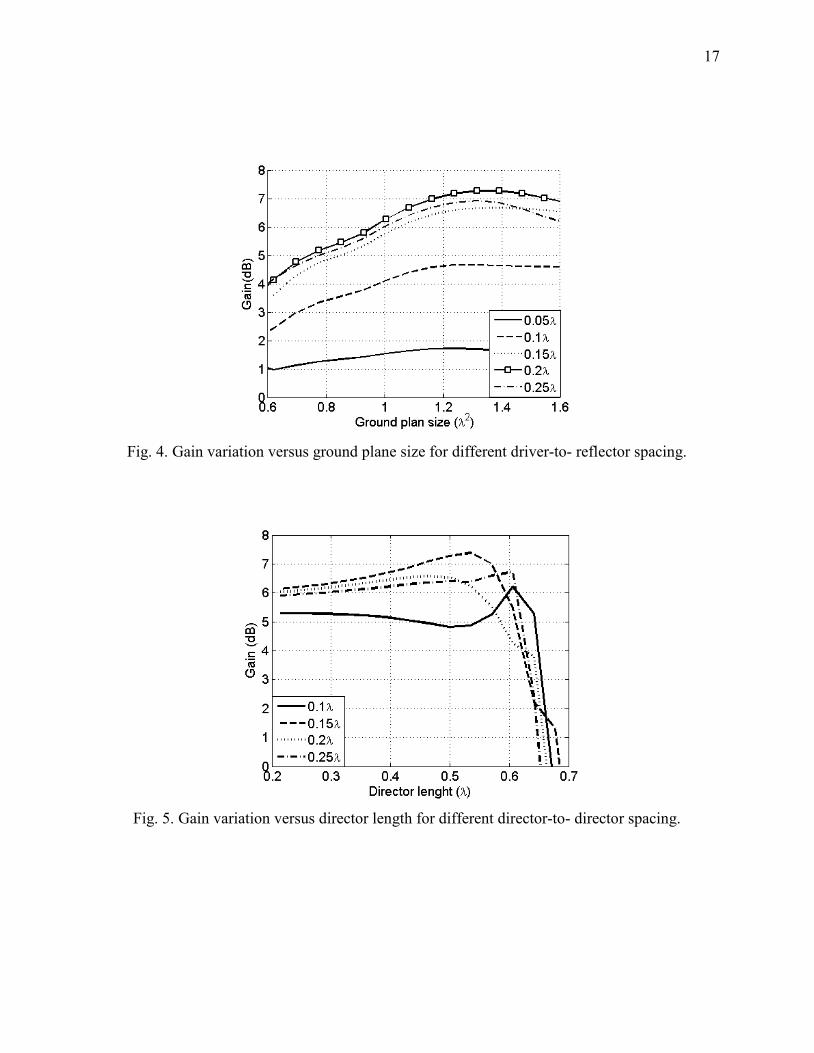
Fig. 4. Gain variation versus ground plane size for different driver-to- reflector spacing.
Fig. 5. Gain variation versus director length for different director-to- director spacing.
18
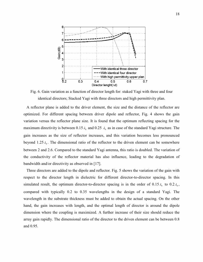
Fig. 6. Gain variation as a function of director length for: staked Yagi with three and four
identical directors; Stacked Yagi with three directors and high permittivity plan.
A reflector plane is added to the driver element, the size and the distance of the reflector are
optimized. For different spacing between driver dipole and reflector, Fig. 4 shows the gain
variation versus the reflector plane size. It is found that the optimum reflecting spacing for the
maximum directivity is between 0.15 0λ and 0.25 0λ as in case of the standard Yagi structure. The
gain increases as the size of reflector increases, and this variation becomes less pronounced
beyond 1.25 0λ . The dimensional ratio of the reflector to the driven element can be somewhere
between 2 and 2.6. Compared to the standard Yagi antenna, this ratio is doubled. The variation of
the conductivity of the reflector material has also influence, leading to the degradation of
bandwidth and/or directivity as observed in [17].
Three directors are added to the dipole and reflector. Fig. 5 shows the variation of the gain with
respect to the director length in dielectric for different director-to-director spacing. In this
simulated result, the optimum director-to-director spacing is in the order of 0.15 0λ to 0.2 0λ ,
compared with typically 0.2 to 0.35 wavelengths in the design of a standard Yagi. The
wavelength in the substrate thickness must be added to obtain the actual spacing. On the other
hand, the gain increases with length, and the optimal length of director is around the dipole
dimension where the coupling is maximized. A further increase of their size should reduce the
array gain rapidly. The dimensional ratio of the director to the driven element can be between 0.8
and 0.95.
19
As shown in Fig. 6, the gain enhancement is not significant when the fourth director is added,
compared to the Yagi antenna with three stacked elements. The addition of an identical fourth
director would increase the gain only by 0.25dB. Upper planar substrate with a high permittivity
is added in order to reduce the antenna size (footprint) and to increase the gain [19], [20]. Fig. 6
shows the effects of adding this substrate without directors on the antenna gain. An improvement
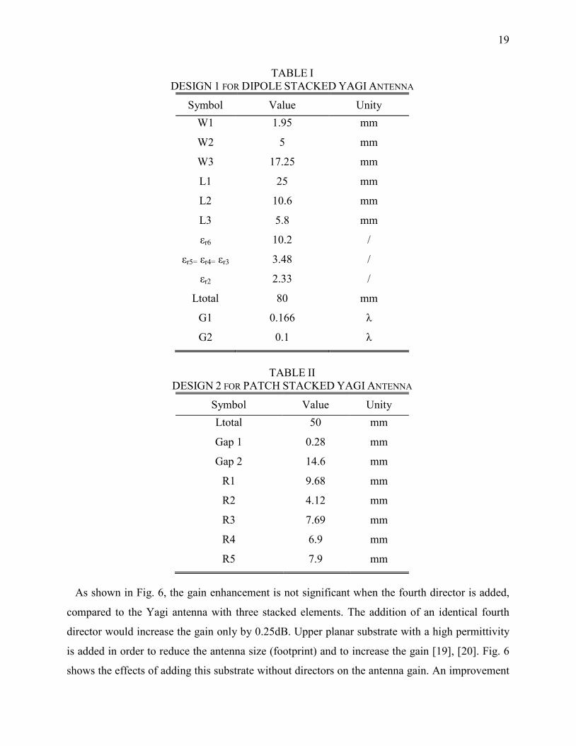
TABLE II DESIGN 2 FOR PATCH STACKED YAGI ANTENNA
Symbol Value Unity Ltotal 50 mm
Gap 1 0.28 mm
Gap 2 14.6 mm
R1 9.68 mm
R2 4.12 mm
R3 7.69 mm
R4 6.9 mm
R5 7.9 mm
TABLE I DESIGN 1 FOR DIPOLE STACKED YAGI ANTENNA
Symbol Value Unity W1 1.95 mm
W2 5 mm
W3 17.25 mm
L1 25 mm
L2 10.6 mm
L3 5.8 mm
εr6 10.2 /
εr5= εr4= εr3 3.48 /
εr2 2.33 /
Ltotal 80 mm
G1 0.166 λ
G2 0.1 λ
20
of 2 dB can be achieved and the optimal length of the directors becomes shorter.
The gain enhancement is given by the following equations [20].
1 21
0 1 1 2
8 ( ) ⋅
≈ ⋅ ⋅ ∆ ⋅ ⋅
n Bgain f bn
ελ ε µ
(2)
in which
1 2 11
0 1 2
2⋅
= ⋅ ⋅ ⋅ ⋅n B nb ε
πλ ε µ
(3)
and
2
1
11( )
1 (2 / ) tan ( )−+=
+ ⋅xf x
xπ (4)
with B being the thickness of the lower layer and 1ε , 1µ are its relative permittivity and permeability, respectively. 2ε and 2µ are the relative permittivity and permeability of the upper layer. 111 µε=n is the refractive index. ∆ is defined as the frequency deviation parameter.
0
1∆ = −ff
(5)
where frequency f is near the center frequency 0f .
Composite planar dielectric structures can be used for increasing the directivity of a point
source when a resonance condition is established. Particular attention has been given to the
physical interpretation of this resonance gain effect in [18]. This is described in terms of leaky
waves (LW) excited in the structure. Under certain resonance conditions, a pair of weakly
attenuated TE/TM leaky waves becomes the dominant contribution to the antenna aperture field.
Equation (2) applied to our specific configuration yields an approximate enhancement of 0.9dB.
A director is added on the upper substrate. Various parameters are optimized starting from the
initial value defined in previous paragraphs. The entire structure of design#1 is optimized in order
to achieve high gain and large bandwidth at 5.8GHz. Director lengths are perturbed to optimize
the return loss with minimum gain loss. The distances between elements along the vertical axis
are: G1=0.166λ (8.58 mm) between reflector layer I and driver layer II; G2=0.1λ (5.6 mm)
between driver layers II, and director layers III, IV and V.
Fig. 7 shows the influence of elements width on the bandwidth of the design #1. This design
can achieve a bandwidth between 6% and 27% at 5.8GHz. It was noticed that this parameter has
has the most significant effect when it is selected between 0.05λ and 0.1 λ, and becomes much
less influential outside this band. The return loss is more sensitive to the width of the elements

21
(driver and director) rather than antenna directivity.
The total height of the designed structure is 29mm. Compared with equation (1), it can be
observed that the spacing between elements can reduced by a factor of two. The upper director
layer is in direct contact with director V. The change of relative permittivity in the interface
between the air gap and the substrate results in a higher equivalent relative permittivity, thus
reducing the air gap. The size of the stacked substrates is 80x80mm.
Fig.7. S11 as a function of element width.
1.3.2.2 Circular Patch Stacked Yagi Antenna with Dual Polarization (Design #2)
In this design demonstration, the classical dipole is replaced by a patch antenna. The proposed
concept offers a possibility to use a wide range of patches instead of the classical dipole as driver.
The circular patch has been used as both, a dual polarization feeder, and also an optimization
facility, since that is only required to optimize one dimension (radius).
The antenna consists of two substrate layers. The circular patch is etched on the top substrate
and the feed lines and ground are etched on the bottom substrate. To achieve the dual polarization
the patch is fed by two orthogonal lines. Such a feeding by coupling allows increasing the
bandwidth. This patch has a bandwidth of 4.5% at 5.8 GHz. The feed layer (layer I in Fig. 3) is
grounded on its bottom side and fed on the other side by 2.26 mm width, 20.27 mm (0.39λ) long
strip lines. The feed lines start from the middle of their respective side, and the width is
calculated to match the antenna to 50Ω. The circular patch has a radius of 0.187λ (9.68mm) and
the spacing between the layers I and II is 0.28mm. The antenna is simulated using Ansoft HFSS

22
v10, a simulator which makes use of the finite element method.
The proposed circular patch stacked Yagi antenna is shown in Fig. 3. This antenna is designed
with the geometry of several layers, and is very similar to the dipole Yagi antenna topology that
was described in the above section. In this structure, the Rogers RF/Duroid 5870 substrate is used
for all the layers with εr =2.33 and thickness of 0.762 mm (30 mil).
As in the case of the first design, the antenna is optimized to achieve better gain and larger
bandwidth, but also the isolation characteristics between the two feed lines must be taken into
account.
One constraint of the stacked dipole Yagi antenna is related to its requirement for a large
ground plane. Fig. 8 shows the gain enhancement of the patch antenna in connection with the
ground size, suggesting that the gain increases with the size of the ground plane. The optimal
ratio of the reflector to the driven element is in the order of 1.6, which is comparable to the
standard Yagi antenna topology. This antenna can be used to reduce overall dimensions of patch
stacked Yagi antenna; a high gain with reduced ground plane can be obtained.
Fig. 8. Gain versus Ground plan size.
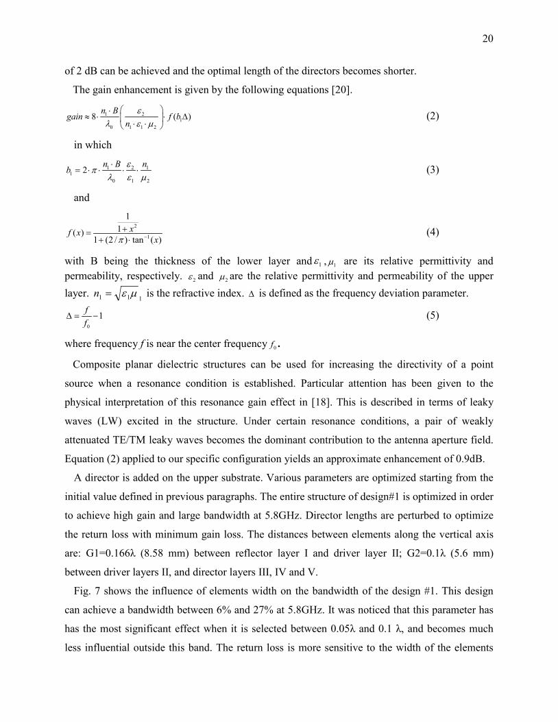
Fig. 9 plots the gain versus the number of parasitic elements for adjacent director-to-director
spacing of 0.3 0λ . Note that adding the sixth director increases the gain only by 0.1dB. Similar to
the first design case, the gain performances are generally controlled by the director spacing and
director length.
23
Fig. 9. Gain versus the Number of parasitic elements.
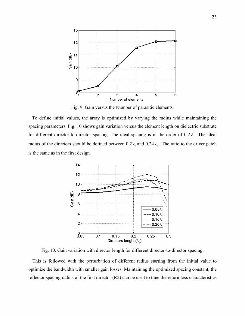
To define initial values, the array is optimized by varying the radius while maintaining the
spacing parameters. Fig. 10 shows gain variation versus the element length on dielectric substrate
for different director-to-director spacing. The ideal spacing is in the order of 0.2 0λ . The ideal
radius of the directors should be defined between 0.2 dλ and 0.24 dλ . The ratio to the driver patch
is the same as in the first design.
Fig. 10. Gain variation with director length for different director-to-director spacing.
This is followed with the perturbation of different radius starting from the initial value to
optimize the bandwidth with smaller gain losses. Maintaining the optimized spacing constant, the
reflector spacing radius of the first director (R2) can be used to tune the return loss characteristics
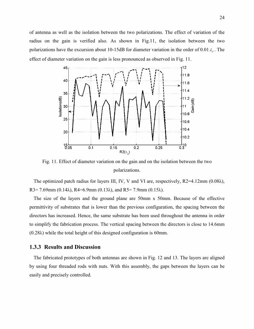
24
of antenna as well as the isolation between the two polarizations. The effect of variation of the
radius on the gain is verified also. As shown in Fig.11, the isolation between the two
polarizations have the excursion about 10-15dB for diameter variation in the order of 0.01 dλ . The
effect of diameter variation on the gain is less pronounced as observed in Fig. 11.
Fig. 11. Effect of diameter variation on the gain and on the isolation between the two
polarizations.
The optimized patch radius for layers III, IV, V and VI are, respectively, R2=4.12mm (0.08λ),
R3= 7.69mm (0.14λ), R4=6.9mm (0.13λ), and R5= 7.9mm (0.15λ).
The size of the layers and the ground plane are 50mm x 50mm. Because of the effective
permittivity of substrates that is lower than the previous configuration, the spacing between the
directors has increased. Hence, the same substrate has been used throughout the antenna in order
to simplify the fabrication process. The vertical spacing between the directors is close to 14.6mm
(0.28λ) while the total height of this designed configuration is 60mm.
1.3.3 Results and Discussion
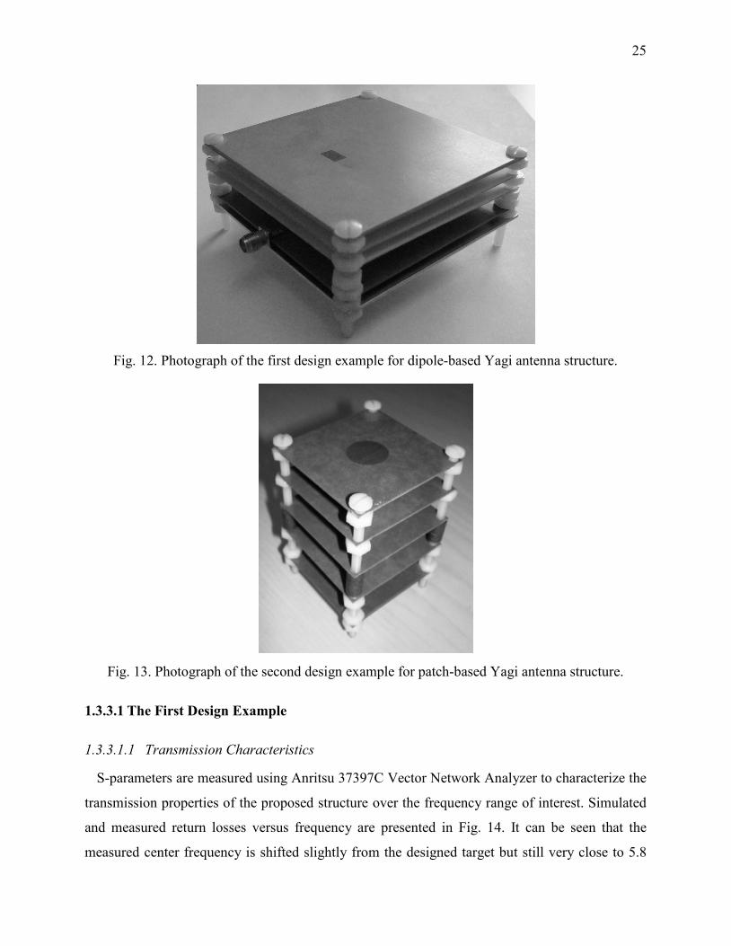
The fabricated prototypes of both antennas are shown in Fig. 12 and 13. The layers are aligned
by using four threaded rods with nuts. With this assembly, the gaps between the layers can be
easily and precisely controlled.
25
Fig. 12. Photograph of the first design example for dipole-based Yagi antenna structure.
Fig. 13. Photograph of the second design example for patch-based Yagi antenna structure.
1.3.3.1 The First Design Example
1.3.3.1.1 Transmission Characteristics
S-parameters are measured using Anritsu 37397C Vector Network Analyzer to characterize the
transmission properties of the proposed structure over the frequency range of interest. Simulated
and measured return losses versus frequency are presented in Fig. 14. It can be seen that the
measured center frequency is shifted slightly from the designed target but still very close to 5.8

26
GHz. The simulation results obtained by HFSS show a good agreement with the measured
results. The antenna bandwidth (< -10 dB) covers frequencies from 5.4 to 6.2 GHz or almost 14
% at 5.8 GHz.
Fig. 14. S-parameter characteristics of the prototyped antenna #1.
1.3.3.1.2 Radiation Pattern
Radiation pattern measurement is made in a MI Technology anechoic chamber. Fig. 15
presents calculated and measured co-polar (E plane) radiation patterns. From these results, we
can notice a good agreement between the measured and simulated radiation patterns.
It is also observed that the radiation pattern is very directive and symmetric. The 3 dB beam
width is approximately 70° for both measured and simulated patterns. The side lobes are very
low. The oscillation of the right lobe is due to the mechanical constraints of our anechoic
chamber.
27
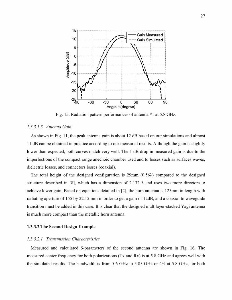
Fig. 15. Radiation pattern performances of antenna #1 at 5.8 GHz.
1.3.3.1.3 Antenna Gain
As shown in Fig. 11, the peak antenna gain is about 12 dB based on our simulations and almost
11 dB can be obtained in practice according to our measured results. Although the gain is slightly
lower than expected, both curves match very well. The 1 dB drop in measured gain is due to the
imperfections of the compact range anechoic chamber used and to losses such as surfaces waves,
dielectric losses, and connectors losses (coaxial).
The total height of the designed configuration is 29mm (0.56λ) compared to the designed
structure described in [8], which has a dimension of 2.132 λ and uses two more directors to
achieve lower gain. Based on equations detailed in [2], the horn antenna is 125mm in length with
radiating aperture of 155 by 22.15 mm in order to get a gain of 12dB, and a coaxial to waveguide
transition must be added in this case. It is clear that the designed multilayer-stacked Yagi antenna
is much more compact than the metallic horn antenna.
1.3.3.2 The Second Design Example
1.3.3.2.1 Transmission Characteristics
Measured and calculated S-parameters of the second antenna are shown in Fig. 16. The
measured center frequency for both polarizations (Tx and Rx) is at 5.8 GHz and agrees well with
the simulated results. The bandwidth is from 5.6 GHz to 5.85 GHz or 4% at 5.8 GHz, for both
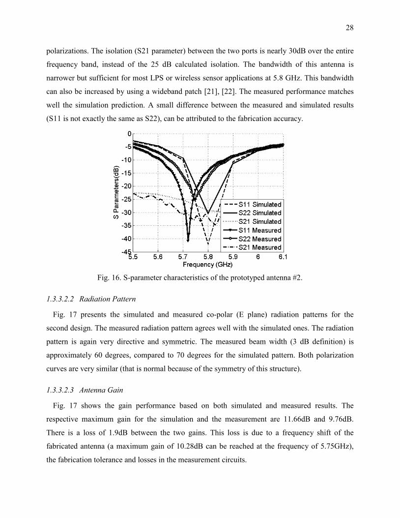
28
polarizations. The isolation (S21 parameter) between the two ports is nearly 30dB over the entire
frequency band, instead of the 25 dB calculated isolation. The bandwidth of this antenna is
narrower but sufficient for most LPS or wireless sensor applications at 5.8 GHz. This bandwidth
can also be increased by using a wideband patch [21], [22]. The measured performance matches
well the simulation prediction. A small difference between the measured and simulated results
(S11 is not exactly the same as S22), can be attributed to the fabrication accuracy.
Fig. 16. S-parameter characteristics of the prototyped antenna #2.
1.3.3.2.2 Radiation Pattern
Fig. 17 presents the simulated and measured co-polar (E plane) radiation patterns for the
second design. The measured radiation pattern agrees well with the simulated ones. The radiation
pattern is again very directive and symmetric. The measured beam width (3 dB definition) is
approximately 60 degrees, compared to 70 degrees for the simulated pattern. Both polarization
curves are very similar (that is normal because of the symmetry of this structure).
1.3.3.2.3 Antenna Gain
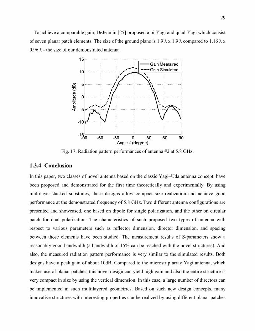
Fig. 17 shows the gain performance based on both simulated and measured results. The
respective maximum gain for the simulation and the measurement are 11.66dB and 9.76dB.
There is a loss of 1.9dB between the two gains. This loss is due to a frequency shift of the
fabricated antenna (a maximum gain of 10.28dB can be reached at the frequency of 5.75GHz),
the fabrication tolerance and losses in the measurement circuits.
29
To achieve a comparable gain, DeJean in [25] proposed a bi-Yagi and quad-Yagi which consist
of seven planar patch elements. The size of the ground plane is 1.9 λ x 1.9 λ compared to 1.16 λ x
0.96 λ - the size of our demonstrated antenna.
Fig. 17. Radiation pattern performances of antenna #2 at 5.8 GHz.
1.3.4 Conclusion
In this paper, two classes of novel antenna based on the classic Yagi–Uda antenna concept, have
been proposed and demonstrated for the first time theoretically and experimentally. By using
multilayer-stacked substrates, these designs allow compact size realization and achieve good
performance at the demonstrated frequency of 5.8 GHz. Two different antenna configurations are
presented and showcased, one based on dipole for single polarization, and the other on circular
patch for dual polarization. The characteristics of such proposed two types of antenna with
respect to various parameters such as reflector dimension, director dimension, and spacing
between those elements have been studied. The measurement results of S-parameters show a
reasonably good bandwidth (a bandwidth of 15% can be reached with the novel structures). And
also, the measured radiation pattern performance is very similar to the simulated results. Both
designs have a peak gain of about 10dB. Compared to the microstrip array Yagi antenna, which
makes use of planar patches, this novel design can yield high gain and also the entire structure is
very compact in size by using the vertical dimension. In this case, a large number of directors can
be implemented in such multilayered geometries. Based on such new design concepts, many
innovative structures with interesting properties can be realized by using different planar patches
30
in the driver layer, or stacked substrate with zero air gap (especially for high frequency
applications such as millimeter-wave or even terahertz frequency ranges). This work suggests
that the proposed concept provides light-weight, low-cost, high-performance and full integration
solutions for local positioning platforms, wireless sensor systems and radar sensor applications. It
can be expected that of those new antennas will provide a very attractive design alterative for a
wide range of microwave and millimetre-wave systems.
Acknowledgment
The author wishes to thank J. Gauthier and S. Dube of Poly-Grames Research Center, École
Polytechnique de Montreal, in the fabrication and mounting of prototypes.
Financial supports from the NSERC of Canada and Regroupement strategique of FQRNT are
greatly appreciated.
References
[1] M. Vossiek, L. Wiebking, P. Gulden, J. Wieghardt, C. Hoffmann and P. Heide, “Wireless
local positioning,” Microwave Magazine ,IEEE, Volume: 4 , Issue: 4, pp:77 – 86, Dec.
2003.
[2] W L. Stutzman and G. A. Thiele, Antenna Theory and Design , Second Edition, John
Wiley and Sons, 1998.
[3] J. Huang, and A.C. Densmore, ”Microstrip Yagi array antenna for mobile satellite vehicle
applications”, IEEE Trans. Antennas Propag., 39, pp. 1024–1030, 1998.
[4] L.C. Kretly and C.E. Capovilla, "Patches driver on the quasi-Yagi antenna: analyses of
bandwidth and radiation pattern", Proceedings ofthe International Microwave and
Optoelectronics Conference, Sep. Vol. 1, pp: 313-316,
[5] Y. Qian, W. Deal, N. Kaneda, and T. Itoh, “Microstrip-fed quasi-Yagi antenna with
broadband characteristics”, Electron. Lett, 34, pp. 2194–2196 , 1998
[6] G. Zheng, A. Kishk, A. Yakovlev, and A. Glisson, “ Simplified feeding for a modified
printed Yagi antenna”, IEEE Antennas Propagat Soc Int Symp Dig 3 , 2003, 934–937.
[7] Q. Yongxi, and T. Itoh, "Active integrated antennas using planar quasi-Yagi
radiators",Proceedings of the International Microwave and Millimeter Wave Technology
Conference, September2000. pp: 1-4.

31
[8] M. Alsliety, and D. Aloi, ”A low profile microstrip yagi dipole antenna for wireless
communications in the 5 Ghz band,” IEEE International Conference on
Electro/information Technology, 2006. pp:525-528
[9] J. P. Damiano, J. Bennegueouche, and A. Papiernik, "Study of multilayer microstrip
antennas with radiating elements of various geometry," IEE Proceedings, Vol. 137, No. 3,
Pt. H, Jun. 1990.
[10] R. Li, G. DeJean, M. Maeng, K. Lim, S. Pinel, M.M. Tentzeris, and J. Laskar, "Design of
compact stacked-patch antennas in LTCC multilayer packaging modules for wireless
applications," IEEE Trans. Advanced Packaging, vol. 27, issue 4, pp. 581 – 589, Nov.
2004.
[11] H. W. Ehrenspeck and H. Poehler, “A new method for obtaining maximum gain from
Yagi antennas,” IRE Trans. Antennas Propagat., vol. AP-7, pp. 379–386, Oct. 1959.
[12] P. S. Bhatnagar, J. P. Daniel, K, Mahdjoubi, and C. Terret, "Experimental study on
stacked triangular microstrip antennas", Electronics Letters, Vol. 22, No. 16, pp. 864-
865, July 1986
[13] C. Guan-Yu, and Jwo-Shiun, “A printed dipole antenna with microstrip tapered balun”,
Microwave and optical technology letters. Vol. 40, No. 4, February 20 2004
[14] N. Michishita, and A. Hiroyuki "A Polarization Diversity Antenna Using a Printed Dipole
and Patch with a Hole,” IEICE Trans. Electronics and Communications, Part 1, Vol.86,
No.9, pp57-66, 2003.
[15] S. Dey, C.K. Aanandan, P. Mohanan, and K.G. Nair "Analysis of cavity backed printed
dipoles", Electronics letters, Vol. 30 No. 3, February 1994.
[16] L. C. Shen, and G. W. Raffoul, “Optimum Design of Yagi Array of Loops”, IEEE
Transactions on Antennas and Propagation V, 22, Iss 6, pp:829- 830, Nov 1974
[17] J.A. Nessel, A. Zaman, R.Q. Lee, and K. Lambert, “Demonstration of an X-Band
multilayer Yagi-like microstrip patch antenna with high directivity and large bandwidth,”
IEEE International Symposium on Antennas and Propagation & USNC/URSI National
Radio Science Meeting. Washington, DC, July 3–8, 2005, pp: 227-230 vol. 1B.
[18] D.R. Jackson, and A.A. Oliner, ”A Leaky-Wave Analysis of High-Gain Printed Antenna
Configuration,” IEEE Trans. Antennas Propagat., vol. 36, n.7, pp. 905-910, July 1988.

32
[19] A. Hoorfar, “Analysis of a “Yagi-Like” Printed Stacked Dipole Array for High-Gain
Application”, Microwave and Optical Technology Letters, Vol.17, No 5, April 5 1998.
[20] D. R. Jackson and N. G. Alexopoulos, ‘‘Gain Enhancement Methods for Printed Circuit
Antennas,’’ IEEE Trans. Antennas Propagat., Vol. AP-33,pp. 976-987. , Sept. 1985.
[21] S. K Padhi, N. C. Karmakar and C.L. Lawan, “An EM coupled dual-polarized microstrip
patch antenna for RFID applications”, Microwave and optical technology letter, vol. 39,
No 5, December 2003.
[22] Antar, Y. M. M., Dajun Cheng, Guozhong jiang, “Wide-band microstrip patch antenna
for personal communication”, The 6th IEEE International Conference on Electronics,
Circuits and Systems, 1999. Proceedings of ICECS ’99. Volume 3, pp: 1305-1308 vol.3.
[23] P.R Grajek, B. Schoenlinner, and G.M Rebeiz, “A 24 GHz high-gain Yagi-Uda antenna
array”, IEEE Trans. Antennas Propag., vol 52, no 5, pp.1257-1261, May 2004.
[24] Gray, D.; J. Lu; D Thiel.; “Electronically steerable Yagi-Uda microstrip patch antenna
array”, IEEE Trans. Antennas Propag., vol. 46, pp 605-608, May 1998.
[25] Gerald R. DeJean, “Design and Analysis of Microstrip Bi-Yagi and Quad-Yagi Antenna
Arrays for WLAN Applications”, IEEE Antennas and Wireless Propagation Letters, vol.
6, 2007
33
CHAPITRE 2 ANTENNES À 60 GHZ
2.1 Présentation
Les antennes présentées au chapitre 1 ont montré le fonctionnement à 5.8 GHz du principe
utilisé. Il apparaît aussi clairement que ce type d’antenne est adapté pour les fréquences plus
élevées car l’espace entre les éléments dans ce cas devient tel qu’aucun espace d’air n’est requis
entre les substrats empilés. Cela permet donc d’avoir une structure multicouche compacte et plus
facilement fabricable avec les techniques de micro-fabrication. Une première antenne
fonctionnant à 60 GHz utilisant une alimentation microstrip a été étudiée, simulée et fabriquée.
Suite à ce travail, un réseau d’antennes 4x4 utilisant l’élément précédent et une alimentation GIS
[Deslandes et Wu (2006)] a été simulé et réalisé. Le GIS est utilisé afin que le réseau de
distribution ne perturbe pas la partie rayonnante du réseau d’antennes. Cela permet une bonne
isolation entre les composants étant donné qu’il n’y a pas de rayonnement parasitique. L’antenne
peut aussi être mise en cascade avec le démodulateur sans utiliser de transitions car le six-port et
l’antenne utilisent la même technologie de guide.

34
2.2 Article 2 - Very Small Footprint 60 GHz Stacked Yagi Antenna
Array
Olivier KRAMER, Tarek DJERAFI, and Ke WU, Fellow, IEEE
“Very Small Footprint 60 GHz Stacked Yagi Antenna Array”
Soumis dans dans “IEEE Transactions on Antennas and Propagation” le 25 novembre 2010.
Manuscript ID AP0903-0249.R2
35
Abstract—Millimeter wave applications such as short-range high-speed wireless links
require modular, compact-size and high-directivity antennas. In this paper, high-gain
compact stacked multilayered Yagi designs are proposed and demonstrated in the V-band.
This novel design shows for the first time an antenna array of Yagi elements in millimeter
wave stacked structure. To demonstrate the proposed concepts and design features, we
create a 4x4 antenna array having excellent gain performance as well as very small
footprint. A single element stacked Yagi antenna fed with microstrip is studied in order to
obtain the desired performance. An analysis is performed to define the structure
limitations. Measured results of the fabricated antenna prototypes are in good agreement
with simulated results The measured Yagi antenna attains 11 dBi gain over 4.2%
bandwidth with a size of 6.5x6.5x3.4 mm3. A 4x4 array of Yagi antenna using an SIW
(Substrate Integrated Waveguide) feeding technique is conceived. Both simulated and
measured results match with each other very well. The 4x4 array has a size of
50x50x60mm3, and reaches a measured gain of 18 dBi over 7% bandwidth. An alternate
configuration of the array using angled Yagi antenna elements allows a significant
improvement of the side lobe level (SLL) with a low impact on the gain performances. The
proposed antennas are excellent candidates for integrated low-cost millimeter-wave and
even terahertz systems. The small foot print, the antenna design flexibility as well as its easy
adaptation to automatic fabrication processes are good assets for making short range
portable imaging systems.
Index Terms—Array, SIW, microstrip antenna, Yagi-Uda, stacked antenna, circular
patch, SLL, feeding network, millimeter-wave and terahertz.
2.2.1 Introduction
he recent trend on the development of millimeter-wave frequencies systems has led to many
innovative techniques with their successful demonstrations in different applications. Among
those applications, the unlicensed bands around 60 GHz and above provides an opportunity for
high-data-rate wireless communications and sensing applications with reduced energy per bit [1];
77 GHz automotive radar [2]; and 94 GHz imagers and radiometers [3], where a lower profile
T

36
array antenna can achieve high gain. Millimeter-wave front-ends necessitate antenna systems
with small size, low-power consumption and power-efficiency requirements [4], which should be
integrated together with circuits to avoid unnecessary transmission line loss. A low side lobe
level (SLL) is another important characteristic parameter that must be controlled to minimize the
interferences [5]. This is particularly in line with the emerging worldwide discussion on green
information and communication technology (Green ICT) policy and its implementations.
The physical gain saturation of planar antennas and more specifically planar antenna array is
defined by Hall [6], and it is limited to circa 35 dBi for a large number of elements with a
significant decrease in efficiency [7]. The stacked Yagi-Uda antenna can overcome this limit by
using the third dimension. The classical Yagi antenna has been widely successful thanks to its
simplicity and customizable high gain [8]-[12]. It consists of basically three-elements: a half-
wavelength driver dipole, a longer reflector backing the driver and a director on the other side.
Presented in a previous paper [13] is a stacked Yagi antenna working at 5.8 GHz for the purpose
of proof-of-concept, stacking together the reflector, the driver, and the directors printed on
substrate. However, the usual spacing between parasitic elements of 0.2λ is quite large at 5.8
GHz and imposes air gaps as the substrate would be too thick. This integration issue is naturally
solved at higher frequencies like millimeter-wave and beyond where a completely integrated
stacked structure can be achieved owe to wavelength comparable with dielectric substrate
thickness. Such structures are suitable for multilayer processing techniques including PCB,
LTCC and photoimageable thick-film process, which have become more mature in integrated
circuit design, fabrication and integration [14][15].

37
Fig. 1. Proposed circular-patch based Yagi antenna.
First of all, a V-band single antenna element is designed and demonstrated, using six elements
fed by microstrip line. An analysis of the dielectric loss as well as the effect of coupling in the
structure is performed in order to design the 4x4 planar antenna array. The array makes use of an
SIW (Substrate Integrated Waveguide) network in order to feed a 4x4 array by coupling the
radiating elements through rectangular slots. The SIW is used to reduce or even suppress the
radiation that generally appears in microstrip feeding structure. Hence, it can be connected to a
demodulation circuit without interferences. An alternate configuration of the array is also
presented. It is composed of Yagi elements oriented in different directions with geometrical
offset with respect to each other, allowing for a significant reduction of SLL.
2.2.2 Stacked Yagi Antenna
The general configuration of the stacked Yagi antenna is shown in Fig. 1 and Fig. 2. It is made
of one circular patch driver, and four parasitic elements. Of course, other forms of radiating
elements can be used instead of circular patch. The antenna respects the same design rules that
are used in the conventional dipole based Yagi antenna, except that it is made on stacked planar
substrates. The circular patch element offers flexibility of design and optimization without
complexity since it requires optimizing one parameter (radius) only and allows the possibility of
a dual polarization. By choosing the elements’ diameters, the spacing between them, the substrate

38
thickness as well as the dielectric constant, the antenna’s performances such as gain, front-to-
back ratio, beam width and center frequency, can be modified.
Fig. 2. Side view of the circular- patch based Yagi antenna.
The elements are printed on Duroïd 5880 substrates and have a relative permittivity of 2.2,
which reduces spacing between parasitic elements. The spacing is within the standard range
which is between 0.15λ and 0.3λ. In this case, the spacing is 0.15λ corresponding to a thickness
of 0.508 mm. The radiating element configuration consists of two substrate layers with 0.254 mm
of thickness. The circular patch is etched on the top of Layer 2, the feed lines etched on top of
Layer 1 and the ground plane at its bottom. The patch is fed by coupling, allowing an increased
bandwidth. The proposed stacked dipole Yagi antenna is simulated using Ansoft HFSS v12.0.
Fig. 3 shows the gain as a function of the number of elements in the stacked Yagi structure. It
can be noticed that the gain rises steadily when the number of elements increases up to 8-9
elements, then begins to get saturated. Stutzman made a similar curve for classical Yagi antennas
and a gain of 12.5 dBi was reached for 10 elements [10]. In our configuration, the gain for the
same number of elements is 2 dB more. In addition, the saturation occurs after a higher number
of elements. This is due to the fact that the circular patch has more gain than its dipole
counterpart, the reflector (here the ground plane of the patch) is four times larger than the
radiating elements, and the fact that the air-substrate interface is placed around the antenna
confines the electromagnetic fields within the structure. The 0.2 to 0.5 dB of gain drop caused by
the dielectric loss shows that it does not have a significant effect on the antenna performances.
This is in particular interesting for millimeter-wave integrated antenna-circuit platform based on
semiconductor substrates. The optimized dimensions of the prototype antenna are tabulated in

39
Table I.
Fig. 3. Gain versus Number of Element.
The total height of the designed structure is 3.4 mm. The surface size of the stacked substrates
is 6.5x6.5 mm². The picture of the fabricated prototype is shown in Fig. 4. S-parameters are
measured using Anritsu 37397C Vector Network Analyzer (VNA) to characterize the matching
condition of the proposed structure over the V-band frequency range. Simulated and measured S-
parameters versus frequency are presented in Fig. 5. We can notice a very small shift in
frequency from the designed target but it is still very close to 59 GHz, which may be caused by
our fabrication tolerance and uncertainty of material parameters. The antenna bandwidth (< -10
dB) covers frequencies from 57.5 to 60 GHz or almost 4.2 % at 60 GHz. The radiation pattern is
TABLE I STACKED YAGI ANTENNA
Symbol Value Unity Dimensions 6.5x6.5x3.4 mm3
L 3 mm
R1 0.75 mm
R2 0.54 mm
R3 0.57 mm
R4 0.62 mm
R5 0.77 mm
εr 2.2 /
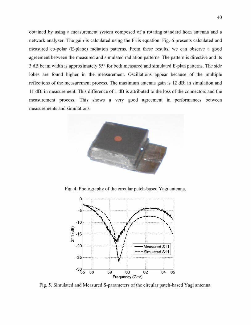
40
obtained by using a measurement system composed of a rotating standard horn antenna and a
network analyzer. The gain is calculated using the Friis equation. Fig. 6 presents calculated and
measured co-polar (E-plane) radiation patterns. From these results, we can observe a good
agreement between the measured and simulated radiation patterns. The pattern is directive and its
3 dB beam width is approximately 55° for both measured and simulated E-plan patterns. The side
lobes are found higher in the measurement. Oscillations appear because of the multiple
reflections of the measurement process. The maximum antenna gain is 12 dBi in simulation and
11 dBi in measurement. This difference of 1 dB is attributed to the loss of the connectors and the
measurement process. This shows a very good agreement in performances between
measurements and simulations.
Fig. 4. Photography of the circular patch-based Yagi antenna.
Fig. 5. Simulated and Measured S-parameters of the circular patch-based Yagi antenna.

41
2.2.3 4x4 stacked Yagi Antenna Array using SIW feeding Mechanism
The antenna array uses SIWs to feed the different elements, which are very suitable for
millimeter wave frequencies thanks to their integrability, low loss, negligible radiation [16], and
hence a more suitable solution than the previous microstrip or other planar feeding techniques. In
order to couple the circular patch, driver slots are made on the top layer of the SIW feeding
network. Because of the feeding structure, this configuration does not allow the use of a reflector.
(a)
(b)
Fig. 6. Measured and simulated gain of the circular-patch based Yagi antenna. (a) H-plane. (b) E-
plane.

42
The proposed feeding is shown in Fig. 7. The geometry of each antenna is very similar to the
previous geometry as described in the above section. The antenna is optimized to achieve the best
possible gain and good bandwidth. Each antenna element reaches a simulated gain of 10.5 dBi,
which conforms to the theory without resorting to a dedicated reflector. Each branch possesses
four elements. The branches are short-circuited at their extremities. Each element is fed by slots
located where the gradient of electric field is the maximum in the waveguide, corresponding to a
spacing of λ/2 in the substrate [17]. This configuration allows for an easy feeding of each
element. Since the distance between elements is less than half a wavelength in the air and also
since the energy distribution is not uniform, the gain does not get doubled when the number of
elements is doubled. A gain of more than 14 dBi is reached for each branch with very low side
lobe level characteristics. Four branches are subsequently added in order to make up a 4x4 array.
Fig. 8 shows the coupling between two of those branches. When dielectric substrate between the
elements is used, the isolation is low and reaches a maximum of 30 dB. Air slots are created
through various techniques such as partial substrate removal between branches in order to reduce
the coupling between them. This improves significantly the isolation with a distance of more than
3 mm (0.6λ). This coupling affects the gain performance of the complete array and changes the
impedance of each branch [10]. This change of impedance could be very time consuming as it
requires optimizing again each branch. In addition, metalized slots are inserted around the
patches to avoid the waves to leak out or spread horizontally, which can use the substrate as a
waveguide through parallel-plate slab mode and radiate out at the edges of the structure.
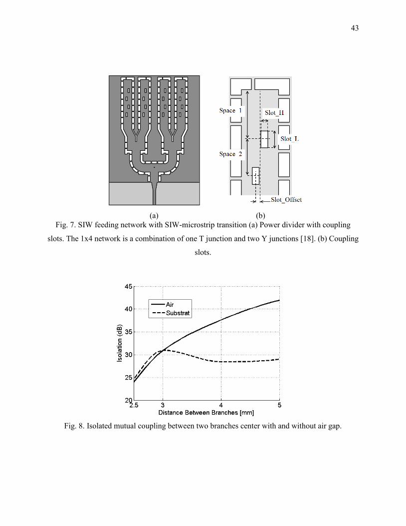
43
(a) (b)
Fig. 7. SIW feeding network with SIW-microstrip transition (a) Power divider with coupling
slots. The 1x4 network is a combination of one T junction and two Y junctions [18]. (b) Coupling
slots.
Fig. 8. Isolated mutual coupling between two branches center with and without air gap.

44
(a)
(b)
Fig. 9. Representation of the entire array antenna including the transition. a) Stack-Up View. b)
Assembled View.
The discussed antenna array is shown in Fig. 9. In this structure, the feeding structure uses
Rogers 6002 with 0.127 mm thickness for the two first layers because of its better properties with
our laser micro-machining used during the fabrication process and Rogers RF/Duroïd 5880
substrate with 0.762 mm thickness for the upper layers. This leads to a total design height of 2.41
mm. The surface size of the upper layers is 28 mm x 24 mm. The resulting array parameters are
listed in Table II. The fabricated prototype is illustrated in Fig. 10.
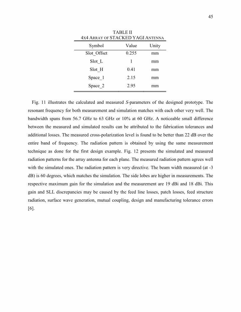
45
Fig. 11 illustrates the calculated and measured S-parameters of the designed prototype. The
resonant frequency for both measurement and simulation matches with each other very well. The
bandwidth spans from 56.7 GHz to 63 GHz or 10% at 60 GHz. A noticeable small difference
between the measured and simulated results can be attributed to the fabrication tolerances and
additional losses. The measured cross-polarization level is found to be better than 22 dB over the
entire band of frequency. The radiation pattern is obtained by using the same measurement
technique as done for the first design example. Fig. 12 presents the simulated and measured
radiation patterns for the array antenna for each plane. The measured radiation pattern agrees well
with the simulated ones. The radiation pattern is very directive. The beam width measured (at -3
dB) is 60 degrees, which matches the simulation. The side lobes are higher in measurements. The
respective maximum gain for the simulation and the measurement are 19 dBi and 18 dBi. This
gain and SLL discrepancies may be caused by the feed line losses, patch losses, feed structure
radiation, surface wave generation, mutual coupling, design and manufacturing tolerance errors
[6].
TABLE II 4X4 ARRAY OF STACKED YAGI ANTENNA
Symbol Value Unity Slot_Offset 0.255 mm
Slot_L 1 mm
Slot_H 0.41 mm
Space_1 2.15 mm
Space_2 2.95 mm
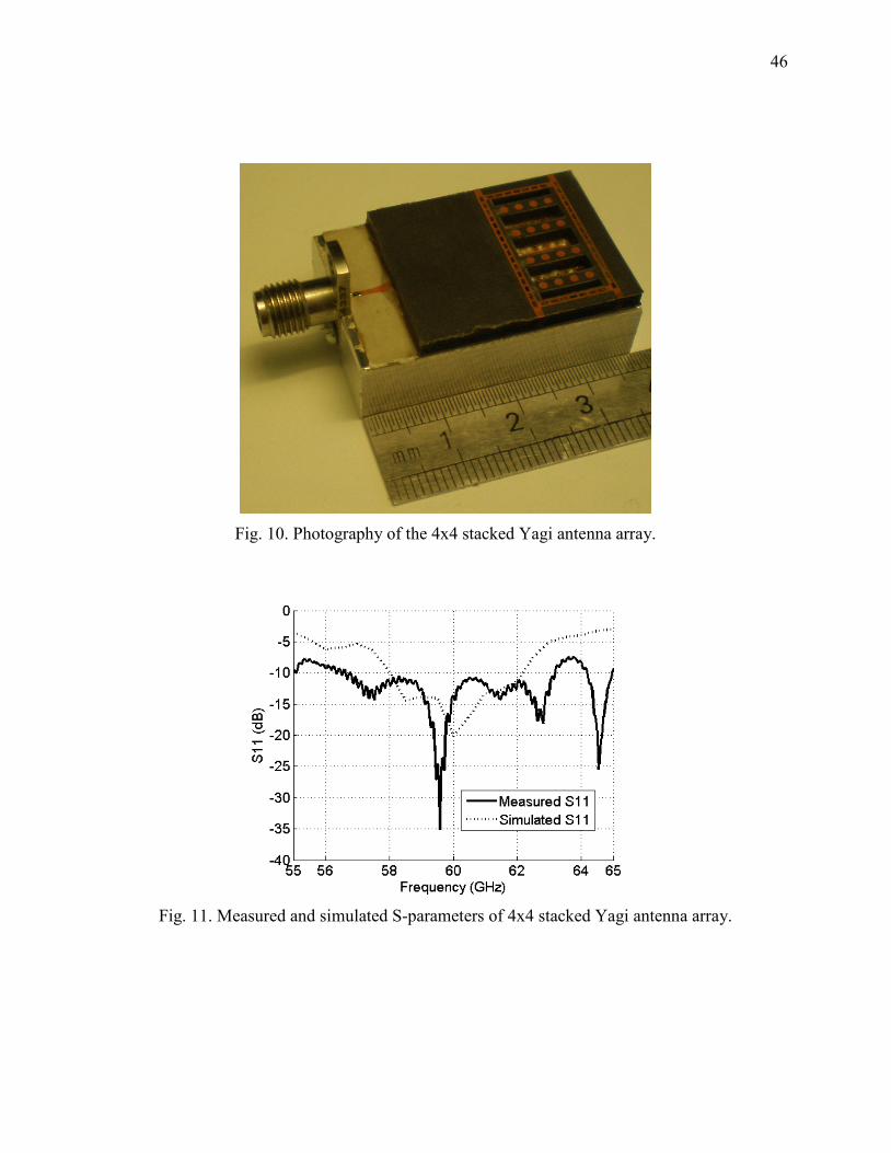
46
Fig. 10. Photography of the 4x4 stacked Yagi antenna array.
Fig. 11. Measured and simulated S-parameters of 4x4 stacked Yagi antenna array.
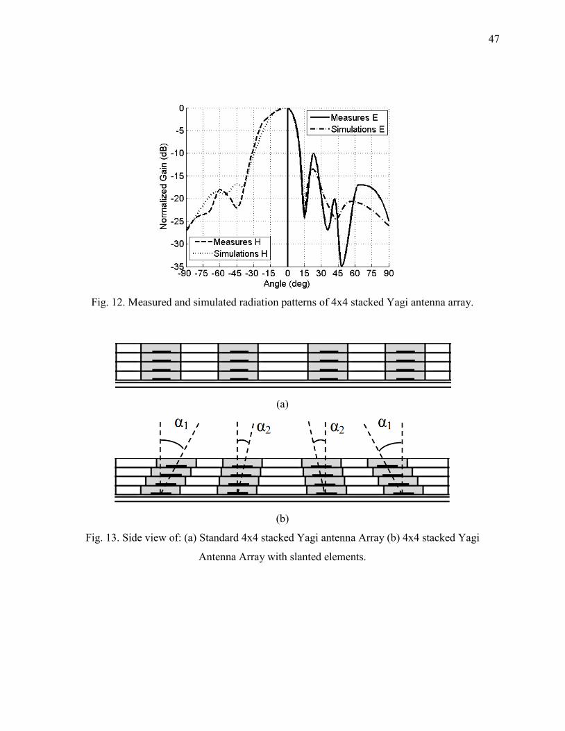
47
Fig. 12. Measured and simulated radiation patterns of 4x4 stacked Yagi antenna array.
(a)
(b)
Fig. 13. Side view of: (a) Standard 4x4 stacked Yagi antenna Array (b) 4x4 stacked Yagi
Antenna Array with slanted elements.
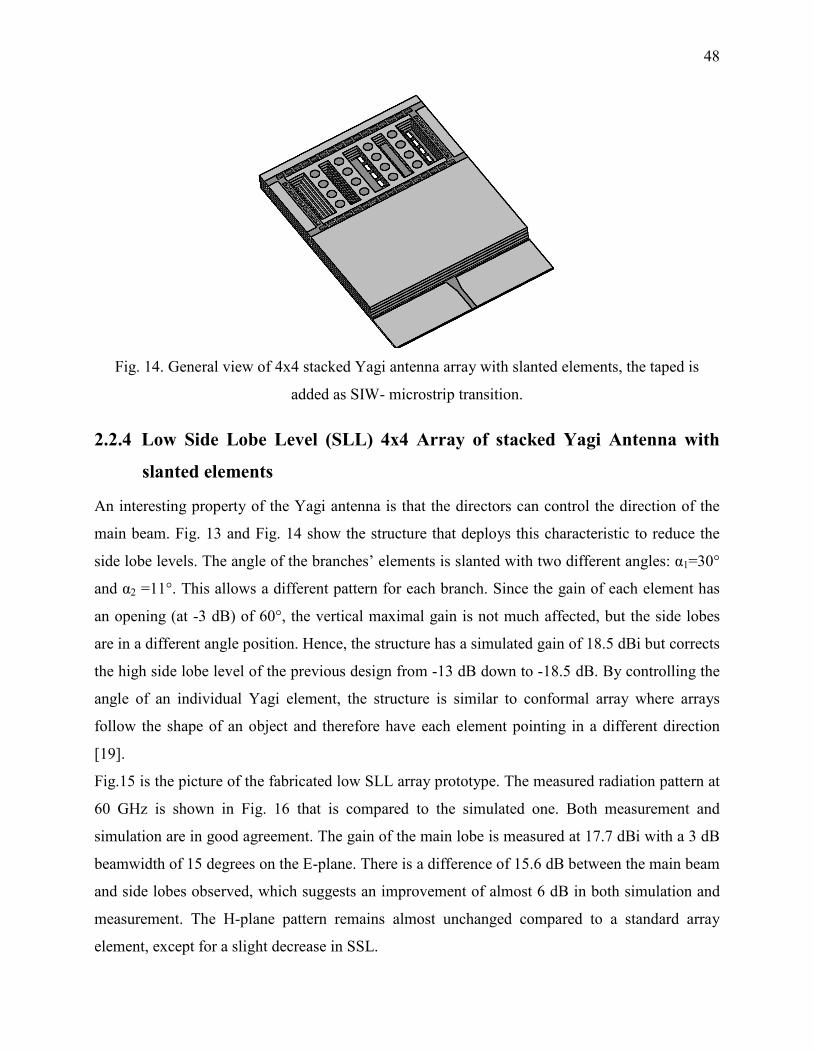
48
Fig. 14. General view of 4x4 stacked Yagi antenna array with slanted elements, the taped is
added as SIW- microstrip transition.
2.2.4 Low Side Lobe Level (SLL) 4x4 Array of stacked Yagi Antenna with
slanted elements
An interesting property of the Yagi antenna is that the directors can control the direction of the
main beam. Fig. 13 and Fig. 14 show the structure that deploys this characteristic to reduce the
side lobe levels. The angle of the branches’ elements is slanted with two different angles: α1=30°
and α2 =11°. This allows a different pattern for each branch. Since the gain of each element has
an opening (at -3 dB) of 60°, the vertical maximal gain is not much affected, but the side lobes
are in a different angle position. Hence, the structure has a simulated gain of 18.5 dBi but corrects
the high side lobe level of the previous design from -13 dB down to -18.5 dB. By controlling the
angle of an individual Yagi element, the structure is similar to conformal array where arrays
follow the shape of an object and therefore have each element pointing in a different direction
[19].
Fig.15 is the picture of the fabricated low SLL array prototype. The measured radiation pattern at
60 GHz is shown in Fig. 16 that is compared to the simulated one. Both measurement and
simulation are in good agreement. The gain of the main lobe is measured at 17.7 dBi with a 3 dB
beamwidth of 15 degrees on the E-plane. There is a difference of 15.6 dB between the main beam
and side lobes observed, which suggests an improvement of almost 6 dB in both simulation and
measurement. The H-plane pattern remains almost unchanged compared to a standard array
element, except for a slight decrease in SSL.

49
Fig. 15. Photograph of the stacked Yagi Antenna 4x4 Array with slanted elements prototype with
a V connector.
Fig. 16. Measured and simulated pattern of stacked Yagi Antenna 4x4 Array with slanted
elements.
2.2.5 Conclusion
A complete study and demonstration of a new stacked multilayer array using the Yagi concept
were carried out in this work. The proposed design is based on several substrate stacked directly
on each other, resulting in a very small footprint of the entire geometry. This configuration was
demonstrated using two types of feeding techniques, showing the outstanding flexibility of the
concept and suggesting its easy integration into millimeter-wave front-ends. The building
elements and the 4x4 antenna array are analyzed, designed and measured. This offers the

50
conception of a high gain antenna (19 dBi was reached) with compact size and minimal footprint.
The measured results of S-parameters show a good bandwidth, a gain of 18 dBi, which are in
very good agreement with the simulated results. The prototyped 4x4 array has a size of
28x24x2.4 mm3 (including the distributed network feeding). Such a very small footprint leads to a
far field around 16 cm at 60 GHz that allows a very close scanning unlike standard horn antenna.
Finally, our design using differently oriented elements highlights its potential in beam forming.
This capability allows for instance the placing of zero in radiation pattern, therefore solving
multipath issues. A large choice of feeding techniques and interesting properties of Yagi antennas
provides this design with the possibilities of dual-polarization, circular polarization, beam
forming and higher array scanning angle, and therefore makes it a viable alternative solution for
many applications. The structure is also suitable for automatic fabrication process and it would be
easy to fabricate by using many micro-fabrication processes including LTCC and photoimageable
thick-film process. Obviously, the proposed scheme presents an excellent light-weight, low-cost,
high-performance antenna technology for millimeter-wave and terahertz systems such as imaging
applications.
Acknowledgment
The author wishes to thank J. Gauthier, T. Antonescu and S. Dubé of Poly-Grames Research
Center, École Polytechnique de Montreal, in the fabrication and mounting of prototypes.
Financial supports from the NSERC of Canada and Regroupement strategique of FQRNT are
greatly appreciated.
References
[1] 60GHz D. Pepe, and D. Zito, “60-GHz transceivers for wireless HD uncompressed
video communication in nano-era CMOS technology,” 15th IEEE Mediterranean
Electrotechnical Conference, April 2010, pp.1237 – 1240.
[2] C. Wagner, R. Feger, A. Stelzer, and H. Jaeger, “A Phased-Array Radar Transmitter
based on 77-GHz Cascadable Transceivers,” IEEE MTT-S International Microwave
Symposium Digest 2009, pp. 73-76.
51
[3] D. S. Goshi, Y. Liu, K. Mai, L. Bui and Y. Shih, “Recent advances in 94Ghz FMCW
imaging radar development,” IEEE MTT-S International Microwave Symposium
Digest 2009, pp. 77 – 80.
[4] E. G. Hoare and R. Hill, “System requirements for automotive radar antennas,” in
IEEE Colloq. Antennas for Automotives, Mar. 2000, pp.1/1–1/11.
[5] F. D. L. Peters, B. Boukari, S. O. Tatu, and T. A. Denidni, “77 ghz millimeter wave
antenna array with wilkinson divider feeding network,” Progress In Electromagnetics
Research Letters, Vol. 9, 193-199, 2009.
[6] P. S. Hall and C. M. Hall, “Coplanar corporate feed effects in microstrip patch array
design,” Proc. IEE, pt. H, vol. 135, pp. 180–186, Jun. 1988.
[7] J. Ashkenazy, P. Perlmutter, and D. Treves, “A modular approach for the design of
microstrip array antennas,” IEEE Antennas and Propagation Trans., AP-31, pp. 190-
193, jan.1983.
[8] H. Yagi, “Beam transmission of ultra short waves,” Proc. IRE, vol. 16, pp. 715–741,
June 1928.
[9] S. Uda, “Radiotelegraphy and radiotelephony on half-meter waves,” Proc. IRE, vol.
18, pp. 1047–1063, 1930.
[10] W L. Stutzman and G. A. Thiele, Antenna Theory and Design , Second Edition, John
Wiley and Sons, 1998.
[11] Q. Yongxi, and T. Itoh, “Active integrated antennas using planar quasi-Yagi
radiators,” Proceedings of the International Microwave and Millimeter Wave
Technology Conference, Sept.2000. pp: 1-4.
[12] L. M. Alsliety, and D. Aloi, “A low profile microstrip yagi dipole antenna for wireless
communications in the 5 Ghz band,” IEEE International Conference on
Electro/information Technology, 2006, pp.525-528
[13] O. Kramer, T. Djerafi, and K. Wu, “Vertically Multilayer-Stacked Yagi Antenna with
Single and dual Polarizations,” IEEE Transactions on Antennas and Propagation,
Vol.58. pp 1022 – 1030, 2010.
[14] M.S. Aftanasar, P.R. Young, I.D. Robertson, J. Minalgiene, and S. Lucyszyn,
“Photoimageable thick-film millimetre-wave metal-pipe rectangular waveguides”,
Electronic Letters, vol. 37, no. 18, pp. 1122-1123, 2001.

52
[15] D. Stephens, P.R. Young, I.D. Robertson, “Millimeter-Wave Substrate Integrated
Waveguides and Filters in Photoimageable Thick-Film Technology”, IEEE
Transactions on Microwave Theory and Techniques, vol. 53, no. 12, pp. 3832-3838,
2005.
[16] M. Bozzi, L. Perregrini, and K. Wu, “Modeling of Conductor, Dielectric, and
Radiation Losses in Substrate Integrated Waveguide by the Boundary Integral-
Resonant Mode Expansion,”, IEEE Transactions on On Microwave Theory and
Techniques, pp.3153- 3161, vol.56, iss.12, Dec. 2008
[17] F. Kolak and C. Eswarappa, “A low profile 77 GHz three beam antenna for
automotive radar,” IEEE MTT-S Dig.2001, vol. 2, pp. 1107–1110.
[18] Germain, S.; Deslandes, D.; Wu, K.; “Development of substrate integrated waveguide
power dividers,” Canadian Conference on, Electrical and Computer Engineering,
2003, vol. 3, pp. 1921 - 1924.
[19] L. Josefsson and P. Persson, Conformal Array Antenna Theory & Design, IEEE
Press/Wiley, 2006.

53
CHAPITRE 3 DÉMODULATION
3.1 Choix du circuit de démodulation
Par rapport aux circuits de conversion classiques à base de mélangeurs, le six-port apporte
une meilleur intégration avec les antennes précédemment conçues et peut utiliser de manière
efficace le multicouche. L’utilisation d’un six-port combiné avec des GIS permet aussi d’avoir de
faibles radiations et donc une bonne isolation entre les composants. En plus d’avoir des
dimensions réduites, un faible coût de fabrication, le six-port possède une excellente stabilité
d'opération à long terme, n’a pas besoin de calibrations fréquentes, et possède ses sources d'erreur
de mesures (non linéarité, sensibilité en température) concentrées sur quelques composants
localisés (détecteurs, etc.) qui peuvent être évaluées et réduites par calcul logiciel. Tout cela fait
du six-port une solution intégrée, adaptée pour ce projet. Ce chapitre présente la théorie des six-
ports et leurs utilisations en tant que démodulateurs. Ensuite la conception d’un nouveau six-port
double couche est étudiée et analysée.
3.2 Présentation du six-port
Certains problèmes apparaissent à hautes fréquences notamment concernant les mesures.
Il devient difficile d'effectuer des mesures de tensions et de courants à des terminaux, et chaque
sonde de mesure peut altérer significativement le champ électrique. La méthode utilisée
actuellement consiste à mesurer les ondes transmises et réfléchies à chaque port. La matrice de
dispersion (appelée souvent matrice S) contient ces informations.
Le besoin de mesurer la matrice de dispersion a donné naissance aux réseaux six-port.
Depuis sa création, le six-port a été largement accepté et à joué un rôle majeur dans le domaine
de la métrologie. La jonction six-port classique est un composant passif constitué de coupleurs et
de lignes de transmissions. Le circuit six-port peut être considéré comme une boite noire à deux
entrées. On utilise une entrée pour le signal à caractériser et l'autre pour le signal de référence.
Les quatre sorties servent à définir le signal [Tatu (2004), Bilik (2008)].

54
3.3 Théorie du six-port
3.3.1 Origine
L'emploi d'un six-port afin de déterminer la phase d'un signal haute fréquence a été
présenté dès 1964 par Cohn et Weinhouse [Cohn et Weinhouse (1964)]. On peut définir la date
de création du six-port comme technique de mesure en 1977 avec la parution de publications
fondamentales [Engen (1977), Hoer (1977)]. Bien que les créateurs, Glenn F. Engen et Cletus A.
Hoer, aient publié des idées partielles et utilisé le terme précédemment, ces publications offrent
les informations théoriques complètes ainsi que la démarche pour concevoir un six-port optimisé.
Ces études ont été poursuivies par Cronson [Cronson et Susman (1981)]. La jonction six-port a
été utilisée avec succès dans la conception d'analyseurs de réseaux. La technique du six-port est
une méthode d'analyse réseau. C'est-à-dire qu'elle permet de mesurer les coefficients de
dispersion.
Il y a deux principales utilisations :
Le réflectomètre six-port : permettant de mesurer seulement le coefficient de réflexion.
L'analyseur de réseau six-port : permettant de mesurer les coefficients de transmission et
de réflexion.
Dans ce document, seule la réflectométrie sera présentée.
3.3.2 Réflectométrie
Le réflectomètre six-port est un moyen de mesure en hyperfréquences qui permet de
déterminer le facteur de réflexion d'un dispositif sous test (qui est directement lié avec son
impédance d'entrée) ou alternativement de trouver le rapport en module et en phase entre deux
différents signaux [Bilik et al. (1990), Zborowska et al. (1989)]. Ce type de mesure est très
souvent utilisé dans le domaine des hyperfréquences, d'un coté dans les laboratoires pour
caractériser des composants et de l'autre coté dans des applications comme les radars de sécurité
pour automobiles, les démodulateurs numériques ou encore le contrôle d’antennes adaptatives.
Le schéma d’un réflectomètre six-port est montré sur la figure ci-dessous. Il s’agit d’un
circuit passif et linéaire avec six accès. Une source RF est connectée au port 1 et le dispositif sous
test dont on veut mesurer le facteur de réflexion est connecté au port 2. Les quatre détecteurs de
puissance, qui sont connectés aux ports 3 à 6, mesurent chacun le module d’une superposition
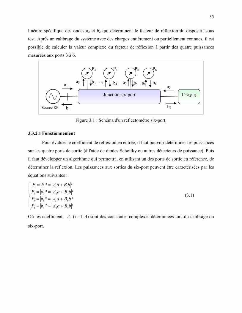
55
linéaire spécifique des ondes a2 et b2 qui déterminent le facteur de réflexion du dispositif sous
test. Après un calibrage du système avec des charges entièrement ou partiellement connues, il est
possible de calculer la valeur complexe du facteur de réflexion à partir des quatre puissances
mesurées aux ports 3 à 6.
Figure 3.1 : Schéma d'un réflectomètre six-port.
3.3.2.1 Fonctionnement
Pour évaluer le coefficient de réflexion en entrée, il faut pouvoir déterminer les puissances
sur les quatre ports de sortie (à l'aide de diodes Schottky ou autres détecteurs de puissance). Puis
il faut développer un algorithme qui permettra, en utilisant un des ports de sortie en référence, de
déterminer la réflexion. Les puissances aux sorties du six-port peuvent être caractérisées par les
équations suivantes :
+==+==+==+==
²²²²²²²²
4444
3333
2222
1111
bBaAbPbBaAbPbBaAbPbBaAbP
(3.1)
Où les coefficients iA (i =1..4) sont des constantes complexes déterminées lors du calibrage du
six-port.
Jonction six-port
b3 b4 b5 a4 a5 a6 b6
Γ=a2/b2
a1
b1 b2 Source RF
a2 a3
P4 P3 P5 P6

56
Figure 3.2 : Schéma d'un six-port.
A partir de la Figure 3.2, on peut définir de manière générale :
ba ⋅Γ= (3.2)
)()( iii
iiiii qbA
AB
babAbBaAb −Γ=+=+= i=1…4 (3.3)
²²²²² iiiiii qAbbBaAbP −Γ⋅⋅=+==⇒ (3.4)
Où :
iA et iB sont des constantes complexes du six-port; Γ est le coefficient de réflexion à
mesurer; et les "points q" valent i
ii A
Bq −=
De par sa conception, chaque sortie du six-port est proportionnelle au carré du signal
incident à mesurer ; i.e. dans notre cas |a|². Si on choisit le port 4 comme référence, on souhaite
que celui-ci ne s'exprime qu'en fonction de b qui est l'onde incidente dans notre DUT ("Device
Under Test"– "Dispositif à mesurer"). On impose donc 04 =A :
²²44 bBP ⋅= (3.5)
En normalisant les autres sorties par rapport à 4P , elles aussi seront exprimées seulement
en fonction de b :
P1 P2
P4 P3
Six-Port DUT
a1 b1 a2 b2
a3 b3 a4 b4
a b
Signal RF
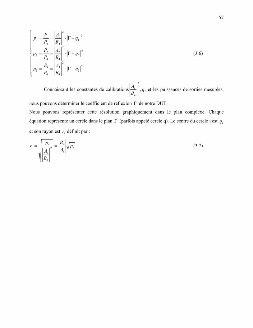
57
−Γ⋅==
−Γ⋅==
−Γ⋅==
23
2
4
3
4
33
22
2
4
2
4
22
21
2
4
1
4
11
qBA
PP
p
qBA
PPp
qBA
PPp
(3.6)
Connaissant les constantes de calibrations2
4BAi , iq et les puissances de sorties mesurées,
nous pouvons déterminer le coefficient de réflexion Γ de notre DUT.
Nous pouvons représenter cette résolution graphiquement dans le plan complexe. Chaque
équation représente un cercle dans le plan Γ (parfois appelé cercle q). Le centre du cercle i est iq
et son rayon est ir définit par :
iii
ii p
AB
BA
pr 4
2
4
== (3.7)

58
Figure 3.3 : Solution graphique aux équations du six-port afin de trouver Γ.
3.3.2.2 Six-port optimal
Un six-port optimum est la configuration qui est la moins sensible aux erreurs de mesure de
puissances. Ceci est étroitement lié à la position des points q. Les critères pour avoir un six-port
optimum peuvent être résumés de la manière suivante :
Le détecteur de référence (souvent le port 4) doit répondre à l'onde incidente du DUT.
C'est-à-dire b .
La phase entre les points q doit être de 120 degré.
La magnitude des points q doit être d'environ 2.
Nous voyons sur la Figure 3.4, le cas optimum avec les points q séparés de 120°, ainsi qu'un
cas critique où il est impossible de savoir laquelle des deux solutions est la bonne. Nous voyons
dans ce dernier cas que la position des points q est importante. De plus, pour obtenir des résultats
précis, un très bon calibrage est nécessaire.
q3
q1
q2
r2
r1
r3
Γ Re
Im

59
Figure 3.4 : Schéma montrant différents placements des points q.
3.4 Jonction six-port modifiée
3.4.1 Présentation
La jonction six-port modifiée est très adaptée pour effectuer des démodulateurs d'un
signal RF modulé QPSK. Une telle jonction s'utilise en tant que discriminateur phase/fréquence.
Elle utilise un diviseur de Wilkinson et trois coupleurs hybrides 90° (Cf. Figure 3.5). Les
matrices de dispersion du diviseur de Wilkinson et du coupleur hybride sont respectivement les
suivantes :
⋅−=
011101110
2jS (3.8)
⋅−=
010001
100010
21
jj
jj
S (3.9)
Re q1
q3
q2
Cas Optimum
0 1 Re
Im
Cas Problématique
?
?
Im
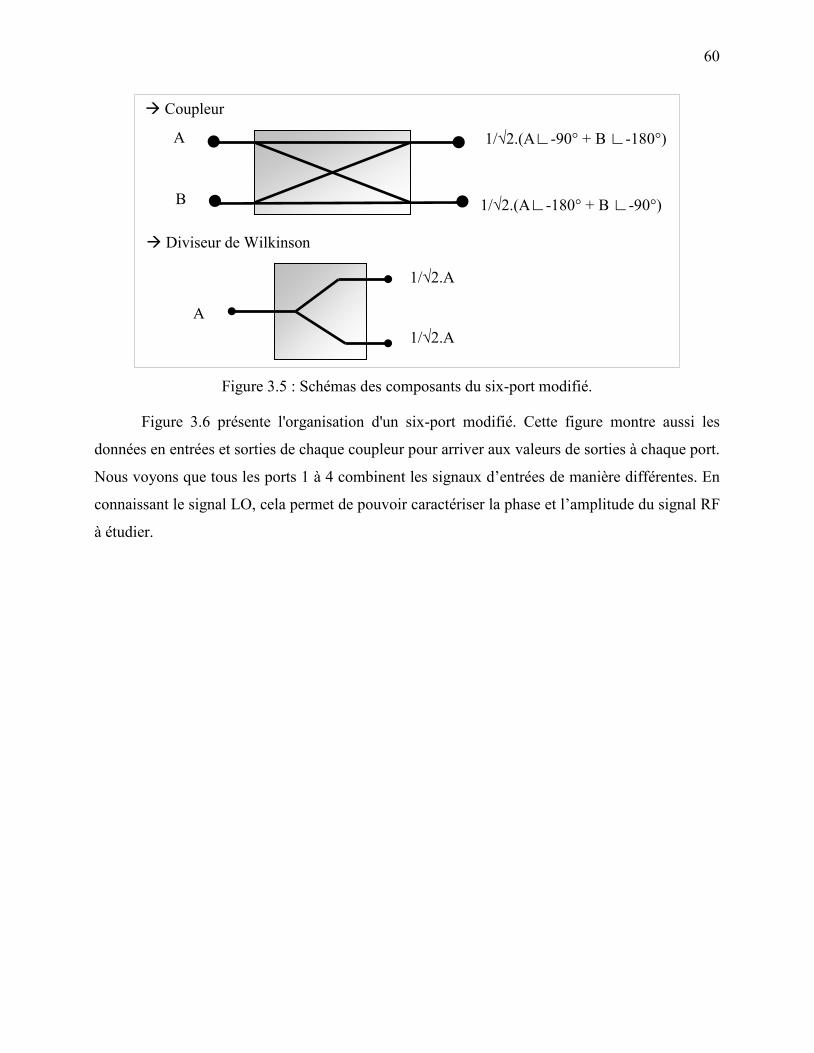
60
Figure 3.5 : Schémas des composants du six-port modifié.
Figure 3.6 présente l'organisation d'un six-port modifié. Cette figure montre aussi les
données en entrées et sorties de chaque coupleur pour arriver aux valeurs de sorties à chaque port.
Nous voyons que tous les ports 1 à 4 combinent les signaux d’entrées de manière différentes. En
connaissant le signal LO, cela permet de pouvoir caractériser la phase et l’amplitude du signal RF
à étudier.
1/√2.(A∟-90° + B ∟-180°)
1/√2.(A∟-180° + B ∟-90°)
A
B
Diviseur de Wilkinson
Coupleur
A
1/√2.A
1/√2.A

61
Figure 3.6 : Jonction six-port modifiée classique.
3.4.2 Démodulateur
Le six-port modifié précédent est utilisé comme démodulateur. Par rapport aux conversions
conventionnelles, le six-port possède les avantages suivants :
la simplicité du circuit;
des dimensions réduites;
un faible cout de fabrication;
un offset DC minime.
Le schéma suivant montre l'organisation d'un démodulateur QPSK à base de six-port.
Diviseur de Puissance
LO Zo
3
5
1
6
2
4
Signal RF
a6
a5
-j.a5/√2 a6/√2
j.a6/√2
-j.a5/√2
0,5.(a5+a6)
-j0,5.( a5-a6)
-j0,5.(a5-ja6)
0,5.(a5+ja6)

62
Figure 3.7 : Démodulateur utilisant une jonction six-port.
3.4.3 Fonctionnement en tant que discriminateur de phase
En considérant chacun des éléments de la Figure 3.6 linéaire, on peut déduire les signaux
aux ports de sorties (1 à 4) :
−−=
+=
+=
+−=
22
22
22
22
654
653
652
651
aajb
aab
ajab
ajajb
(3.10)
En introduisant la propagation du signal dans les diviseurs et coupleurs, on en déduit la
matrice S idéale de la jonction six-port modifiée :
][][][ aSb ⋅= (3.11)
Six
Port
Diodes RF
Amplif. Vidéo
FPB Décodeur
LNA
AGC
LO
DÉMODULATEUR QPSK
I
Q
Signal QPSK
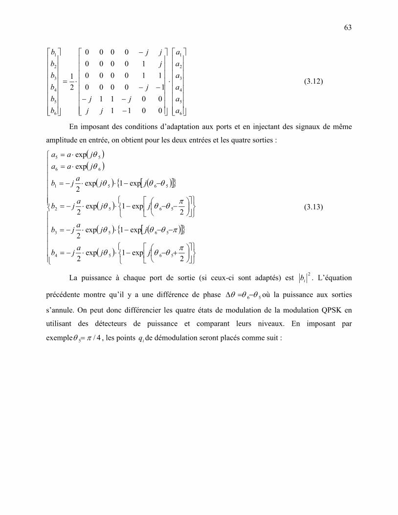
63
⋅
−−−
−−
−
⋅=
6
5
4
3
2
1
6
5
4
3
2
1
0011001110000
11000010000
0000
21
aaaaaa
jjjj
j
jjj
bbbbbb
(3.12)
En imposant des conditions d’adaptation aux ports et en injectant des signaux de même
amplitude en entrée, on obtient pour les deux entrées et les quatre sorties :
( )( )
( ) ( )[ ]{ }
( )
( ) ( )[ ]{ }
( )
+−−⋅⋅−=
−−−⋅⋅−=
−−−⋅⋅−=
−−⋅⋅−=
⋅=⋅=
2exp1exp
2
exp1exp2
2exp1exp
2
exp1exp2
expexp
5654
5653
5652
5651
66
55
πθθθ
πθθθ
πθθθ
θθθ
θθ
jjajb
jjajb
jjajb
jjajb
jaajaa
(3.13)
La puissance à chaque port de sortie (si ceux-ci sont adaptés) est 2ib . L’équation
précédente montre qu’il y a une différence de phase 56 θθθ −=∆ où la puissance aux sorties
s’annule. On peut donc différencier les quatre états de modulation de la modulation QPSK en
utilisant des détecteurs de puissance et comparant leurs niveaux. En imposant par
exemple 4/5 πθ = , les points iq de démodulation seront placés comme suit :

64
Figure 3.8 : Position des points pour θ5=π/4.
En utilisant des détecteurs de puissance aux sorties du six-port (diodes par exemple), la
tension en sortie sera proportionnel au carré de l’amplitude ib :
2iii bKV ⋅= (3.14)
On retrouve donc comme amplitude de tension aux sorties, les équations
suivantes (considérant chacun des détecteurs identique, i.e. KKi = ) :
( )
( )( )
+∆⋅⋅=
+∆−=
−∆
⋅⋅=−∆−=
−∆⋅⋅=
−∆−=
∆⋅⋅=∆−=
2
222
4
222
2
3
2
222
2
222
2
1
22sin
2exp1
4
2sinexp1
4
22sin
2exp1
4
2sinexp1
4
πθπθ
πθπθ
πθπθ
θθ
aKja
KV
aKja
KV
aKja
KV
aKja
KV
(3.15)
Une façon d’obtenir la constellation dans le plan complexe I/Q, est d’affecter
l’information à la phase du signal d’entrée 6θ , avec la phase du signal LO 5θ servant de
référence. Le vecteur Γ exprimé en fonction des quatre voltages de sortie contient l’information
et sa représentation nous donne l’information du signal (Cf. Figure 3.9).
q1 +j
1 Re
Im q2
q4 q3
-1
-j
65
( ) ( )[ ]
⋅−+−=Γ
4exp2413 πjVVjVV (3.16)
Figure 3.9 : Modulation QPSK.
3.5 Présentation de la réalisation d'une jonction six-port modifiée à
60 GHz
Pour ce projet le circuit six-port est basé sur la jonction modifiée mais repose sur une
structure différente faite de diviseurs, de coupleurs double couche et d’un nouveau déphaseur
large bande fait de stubs plan-H. Cela permet d’obtenir six accès exactement sans adaptation de
ports inutilisés.
11
I
Q 01
10 00
66
3.6 Article 3 - Dual-Layered Substrate Integrated Waveguide Six-
Port with Wideband Double Stub Phase Shifter
Olivier KRAMER, Tarek DJERAFI, and Ke WU, Fellow, IEEE
“Dual-Layered Substrate Integrated Waveguide Six-Port with Wideband Double Stub
Phase Shifter”
Soumis dans dans “ IEEE MTT-S Transaction ” le 25 novembre 2010.
Manuscript ID TMTT-2010-11-0644
67
Abstract— A dual layered six-port front-end circuit on the basis of substrate integrated
waveguide (SIW) technology is presented and demonstrated. The use of SIW technology
allows the development of a compact circuit with low radiation loss at millimeter wave
frequencies. The six-port architecture makes use of multilayer couplers that provide a wide
coupling area through two slots; a new broadband SIW phase shifter composed of two H-
plane stub lines and a reference line; and two SIW power dividers. The six-port design is
free from loads as in the case of classic modified six-port architectures with 8 ports. To
validate the proposed concept, an integrated broadband six-port front-end circuit
prototype was designed, fabricated and measured. Simulation and measurement results
show that the proposed six-port circuit can easily operate at 60 GHz for V-band system
applications. The two-layered structure presents interesting technological features
including low profile, small volume and footprint, and high-density integration.
Index Terms— Directional Coupler, Multi-Layer, Phase Shifter, Six-Port, SIW, Stacked
Structure.
3.6.1 Introduction
illimeter-wave access systems at 60 GHz are designed to support short-range point-to-
point or point-to-multipoint data links in connection with broadband multimedia
services[1]. These services include, for example, e-commerce, interactive video transmissions, or
remote learning, and tele-medicine [2].
As an alternative to the classic super-heterodyne and homodyne techniques, six-port radio
architecture was proposed for the development of low-cost and high-efficient direct-conversion
software-defined transceivers, which are now becoming an attractive solution compared to the
conventional mixer-based schemes because of its low power consumption, good linearity and low
system noise as well as low design and manufacturing cost [3]-[4]. The six-port junction circuit is
a passive interferometer device that essentially consists of several couplers, power dividers and
one wideband phase shifter, and it can be considered as a black box with two inputs and four
outputs. The output ports are terminated with power detectors. Characteristic relationship or
correlation between the two input signals (phase and amplitude) can be determined by reading the
M

68
baseband power information from the output ports.
Substrate integrated waveguide (SIW) technology has been found suitable for the design of six-
port radio and radar [5]-[7] systems with the demand for low-loss and low-cost as well as
integration of high-density microwave and millimeter-wave components and subsystems [6]. To
ensure wide-band performances of the six-port on the basis of SIW technology, both coupler and
phase shifter must have wideband properties. In this work, a V-band six-port is proposed, which
is based on the combination of two couplers and two power dividers with a broadband 90 degree
phase shifter using H-plane stubs. The architecture leads to a six-port structure, which is different
from the conventional types of six-port that generally have seven- or eight-ports. In this case,
excessive ports should be terminated by appropriate loads. .
The two-layer coupling structure is a very attractive scheme for the realization of high
performances couplers using a wide coupling aperture, and also an SIW stub-based H-plane
phase shifter is used to achieve the desired phase distribution.
In this work, different components are first designed as fundamental building blocks of the six-
port. Parameters of these components are fine-tuned using Ansoft’s High-Frequency Structure
Simulator (HFSS) package to realize broadband performances. The broadband H-plane phase
shifter is modeled, designed, optimized, and measured. Combining the designed coupler and
phase shifter, the six-port front-end circuit is then developed and optimized. To demonstrate the
performances of the proposed six-port circuit, an experimental prototype is fabricated and
measured. Simulation and measured results are presented and discussed.
Phase Shifter
Power divider
Power divider
Port 1 Port 2
Port 6 Port 5
Port 4 Port 3
Phase Shifter
Fig. 1. Block diagram of the proposed six-port junction circuit.

69
3.6.2 Design Framework
The block diagram of the proposed six-port circuit is shown in Fig. 1. The six-port junction was
designed with Rogers RT/Duroid 6002 substrate with dielectric relative permittivity of 2.94 and
substrate thickness of 0.254 mm (10 mil). As shown in Fig. 1, the six-port circuit is composed of
two hybrid couplers, two powers dividers and one two stub phase shifter. The next sub-sections
will describe in details theses different components.
3.6.2.1 Phase Shifter
The development of our H-plane wideband SIW phase shifter structure is inspired by the E-
plane phase shifter of Dittloff [8]. Fig. 2 shows the stubs used in the phase shifter. It makes use of
two transmission lines, more specifically, a reference line and a line containing several stubs. If
the same signal is guided though the reference line and the line containing the stubs, the two
output signals will have a nearly flat phase difference in frequency. Dittloff’s results show a
differential phase shift of 90° ± 2.5° with 15% bandwidth using two stubs and 90° ± 0.5° with
20% bandwidth using three stubs.
Fig. 2. Geometry of the H-plane SIW stubs.
ds
ls
hs
Δl Y
X
Fig. 3. Geometry of the H-plane SIW phase shifter using two stubs.
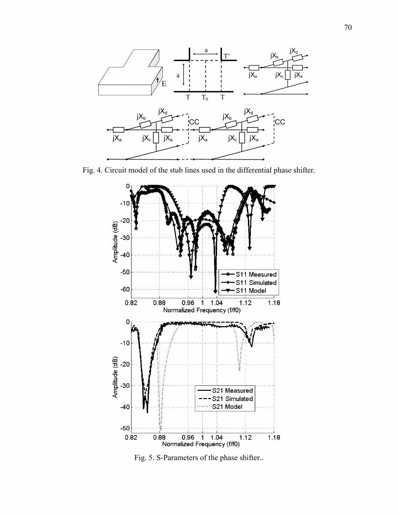
70
E
a
a T’
T0 T T
jXa jXa
jXb jXd
jXc
CC
jXa jXa
jXb jXd
jXc
CC
jXa jXa
jXb jXd
jXc
Fig. 4. Circuit model of the stub lines used in the differential phase shifter.
Fig. 5. S-Parameters of the phase shifter..
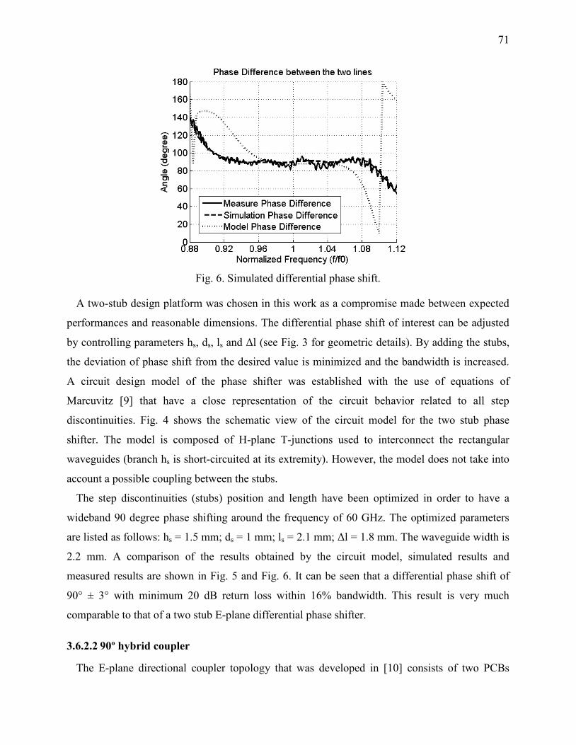
71
Fig. 6. Simulated differential phase shift.
A two-stub design platform was chosen in this work as a compromise made between expected
performances and reasonable dimensions. The differential phase shift of interest can be adjusted
by controlling parameters hs, ds, ls and Δl (see Fig. 3 for geometric details). By adding the stubs,
the deviation of phase shift from the desired value is minimized and the bandwidth is increased.
A circuit design model of the phase shifter was established with the use of equations of
Marcuvitz [9] that have a close representation of the circuit behavior related to all step
discontinuities. Fig. 4 shows the schematic view of the circuit model for the two stub phase
shifter. The model is composed of H-plane T-junctions used to interconnect the rectangular
waveguides (branch hs is short-circuited at its extremity). However, the model does not take into
account a possible coupling between the stubs.
The step discontinuities (stubs) position and length have been optimized in order to have a
wideband 90 degree phase shifting around the frequency of 60 GHz. The optimized parameters
are listed as follows: hs = 1.5 mm; ds = 1 mm; ls = 2.1 mm; Δl = 1.8 mm. The waveguide width is
2.2 mm. A comparison of the results obtained by the circuit model, simulated results and
measured results are shown in Fig. 5 and Fig. 6. It can be seen that a differential phase shift of
90° ± 3° with minimum 20 dB return loss within 16% bandwidth. This result is very much
comparable to that of a two stub E-plane differential phase shifter.
3.6.2.2 90º hybrid coupler
The E-plane directional coupler topology that was developed in [10] consists of two PCBs

72
glued together (using epoxy) with apertures etched on their common wall. Two parallel
compounds (offset-inclined) resonant slots are located in the common broad wall. The coupling
level and the transmission phase can be controlled by adjusting slot length Lslot, inclination angle
α and offset doffset. The use of the inclined slots is able to reduce the size of the coupler. The
coupling slots have a resonant length calculated at the center operating frequency as a function of
the tilt angle and offset together with the waveguide height. The coupling level is tuned by
different width of the slots, their inclination and offset. The gap of epoxy between the two PCBs
constitutes a parallel plate waveguide. A part of the coupled power travels onto this TEM line
which supports undesired higher order modes. To solve this problem, the two common conductor
planes must be avoided in the region of the slots as shown in Fig. 7.
α
doffset Lslot
wslot
Fig. 7. The dual-layered SIW coupler configuration.
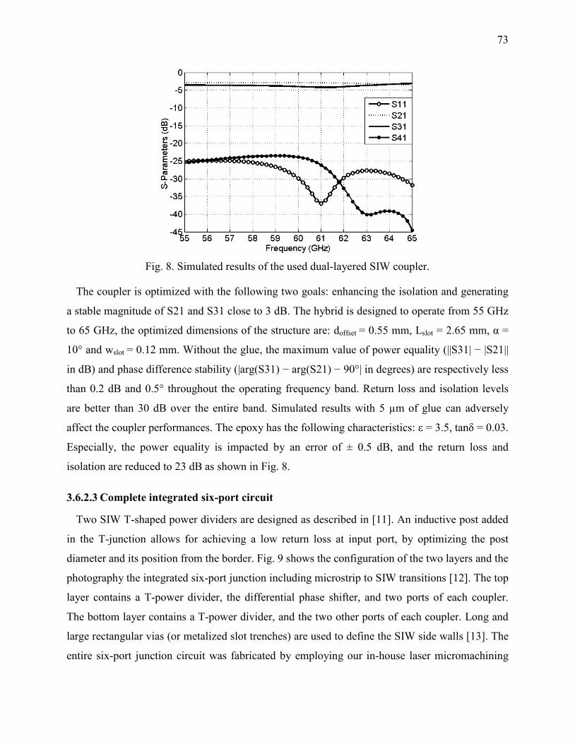
73
Fig. 8. Simulated results of the used dual-layered SIW coupler.
The coupler is optimized with the following two goals: enhancing the isolation and generating
a stable magnitude of S21 and S31 close to 3 dB. The hybrid is designed to operate from 55 GHz
to 65 GHz, the optimized dimensions of the structure are: doffset = 0.55 mm, Lslot = 2.65 mm, α =
10° and wslot = 0.12 mm. Without the glue, the maximum value of power equality (||S31| − |S21||
in dB) and phase difference stability (|arg(S31) − arg(S21) − 90°| in degrees) are respectively less
than 0.2 dB and 0.5° throughout the operating frequency band. Return loss and isolation levels
are better than 30 dB over the entire band. Simulated results with 5 µm of glue can adversely
affect the coupler performances. The epoxy has the following characteristics: ε = 3.5, tanδ = 0.03.
Especially, the power equality is impacted by an error of ± 0.5 dB, and the return loss and
isolation are reduced to 23 dB as shown in Fig. 8.
3.6.2.3 Complete integrated six-port circuit
Two SIW T-shaped power dividers are designed as described in [11]. An inductive post added
in the T-junction allows for achieving a low return loss at input port, by optimizing the post
diameter and its position from the border. Fig. 9 shows the configuration of the two layers and the
photography the integrated six-port junction including microstrip to SIW transitions [12]. The top
layer contains a T-power divider, the differential phase shifter, and two ports of each coupler.
The bottom layer contains a T-power divider, and the two other ports of each coupler. Long and
large rectangular vias (or metalized slot trenches) are used to define the SIW side walls [13]. The
entire six-port junction circuit was fabricated by employing our in-house laser micromachining
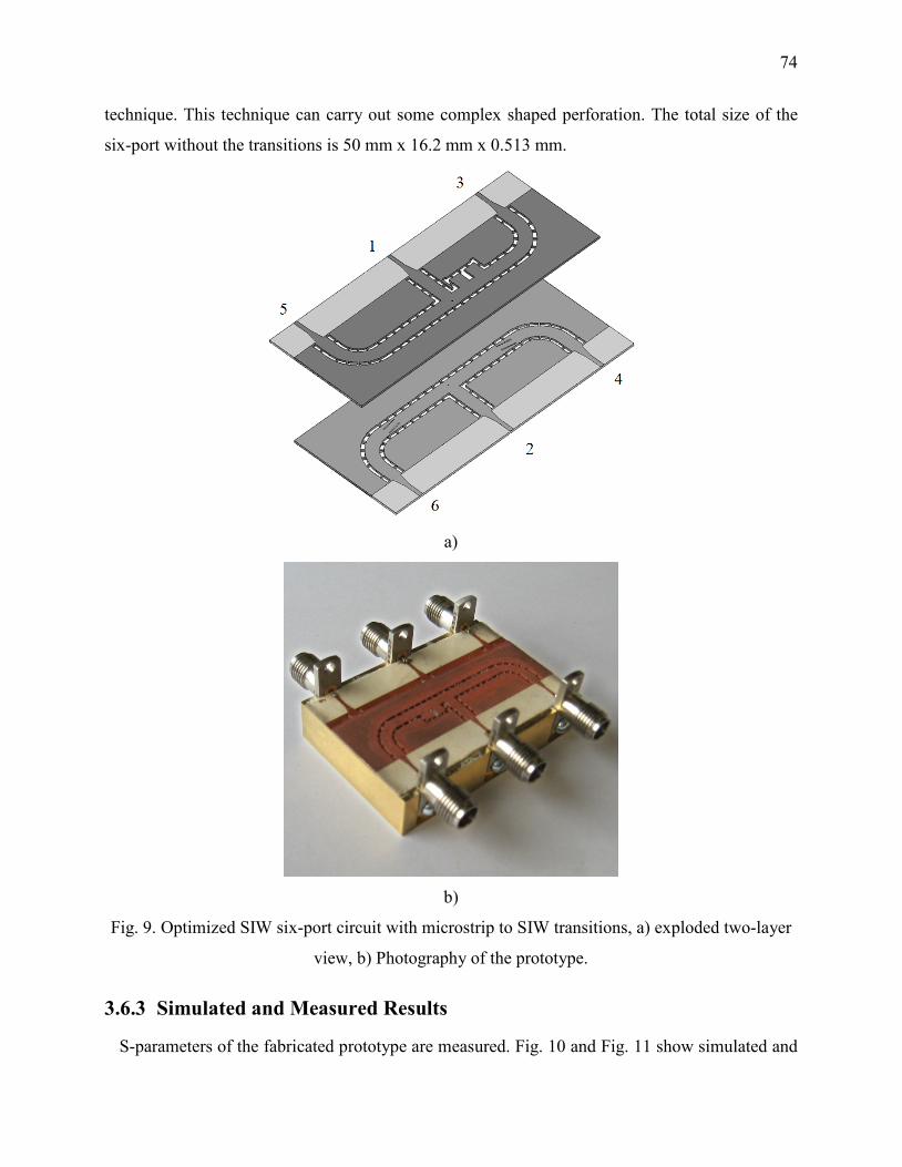
74
technique. This technique can carry out some complex shaped perforation. The total size of the
six-port without the transitions is 50 mm x 16.2 mm x 0.513 mm.
a)
b)
Fig. 9. Optimized SIW six-port circuit with microstrip to SIW transitions, a) exploded two-layer
view, b) Photography of the prototype.
3.6.3 Simulated and Measured Results
S-parameters of the fabricated prototype are measured. Fig. 10 and Fig. 11 show simulated and
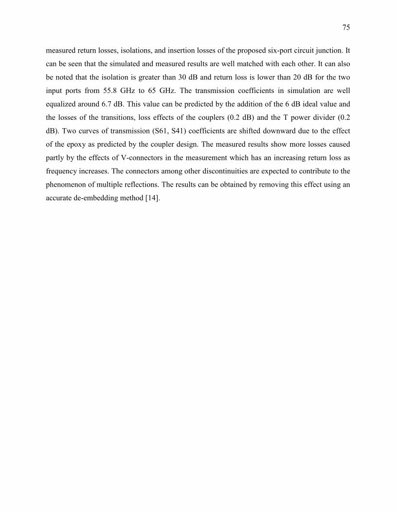
75
measured return losses, isolations, and insertion losses of the proposed six-port circuit junction. It
can be seen that the simulated and measured results are well matched with each other. It can also
be noted that the isolation is greater than 30 dB and return loss is lower than 20 dB for the two
input ports from 55.8 GHz to 65 GHz. The transmission coefficients in simulation are well
equalized around 6.7 dB. This value can be predicted by the addition of the 6 dB ideal value and
the losses of the transitions, loss effects of the couplers (0.2 dB) and the T power divider (0.2
dB). Two curves of transmission (S61, S41) coefficients are shifted downward due to the effect
of the epoxy as predicted by the coupler design. The measured results show more losses caused
partly by the effects of V-connectors in the measurement which has an increasing return loss as
frequency increases. The connectors among other discontinuities are expected to contribute to the
phenomenon of multiple reflections. The results can be obtained by removing this effect using an
accurate de-embedding method [14].
76
a)
b)
Fig. 10. Simulated and measured S-parameters (Return Loss and Isolation).

77
a)
b)
Fig. 11. Simulated and measured S-parameters for 1-3, 1-4, 1-5, and 1-6 path.
Simulated and measured phase differences between the two input and output ports are shown in
Figs. 12 and 13. From these curves, it can be observed that simulation and measurement results
agree very well with each other. It can be seen that the phase differences between S31 and S61,
S42 and S62, S32 and S52, are close to zero. Furthermore, the phase differences between S31 and
S41, S51 and S61, S32 and S42, S62 and S52 are close to 90º. The proposed integrated six-port
circuit has demonstrated an excellent performance over a large bandwidth. It can be concluded
that the obtained results are very promising and that each component works successfully.

78
3.6.4 Conclusion
A wideband two layered SIW six-port has been designed and demonstrated to operate over the
V-band. The wideband performance of the six-port junction is attributed to the wideband design
of its components. Especially, the phase shifter is designed on the basis of the principle of stub
line phase shifter. The introduced H-plane differential phase shifter shows good performances
similar to the existing E-plane counterpart. The circuit model of the differential phase shifter
shows a good agreement but a narrower bandwidth than the simulated and measured results. The
six-port exhibits coupling results and phase errors within −6.7 dB ±0.7 and 10° over a (57-65
GHz) 20% bandwidth with center frequency at 60 GHz. The proposed six-port junction circuit
has been found to have the following advantages: compactness, low radiation loss, ease of
fabrication and low cost. To validate the proposed concept, a six-port prototype was fabricated
and measured.

79
Fig. 12. Simulated S-parameters Phase.
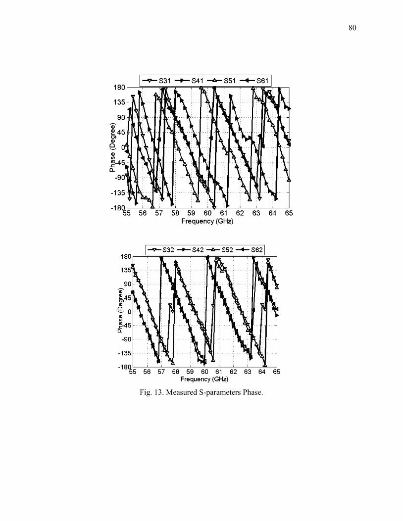
80
Fig. 13. Measured S-parameters Phase.
81
Acknowledgment
The authors wish to thank S. Dubé, T. Antonescu, and J. Gauthier for the circuit prototyping.
Financial supports from the NSERC of Canada and Regroupement strategique of FQRNT are
greatly appreciated.
References
[1] P. Smulders, “Exploiting the 60 GHz band for wireless multimedia access: prospects and
future directions,” IEEE Commun. Mag., vol. 40, no.1, pp. 140–147, Jan. 2002.
[2] N. Guo, Robert C. Qiu Shaomin S. Mo Kazuaki Takahashi, “60-GHz millimeter-wave radio
principle, technology, and new Results,” EURASIP Journal on Wireless Communications
and Networking archive, Volume 2007 , Issue 1 Pages: 48 - 48 .January 2007
[3] Y. Zhao, J.-F. Frigon, K. Wu, and R.G. Bosisio, “Multi (six)-port impulse radio for ultra-
wideband”, IEEE Trans. Microw. Theory Tech., 2006, 4, (54), pp. 1707–1712
[4] S.O. Tatu, Moldovan, K. Wu, R.G. Bosisio and T.A. Denidni, “Ka-band analog front-end
for software-defined direct conversion receiver”, IEEE Trans. Microw. Theory Tech., 2005,
9, (53), pp. 2768– 2776
[5] X. Xu, R.G. Bosisio and K. Wu, “Analysis and implementation of sixport software-defined
radio receiver platform”, IEEE Trans. Microw. Theory Tech., 2006, 7, (54), pp. 2937–2943.
[6] K. Wu, “Integration and interconnect techniques of planar and nonplanar structures for
microwave and millimeter-wave circuits—Current status and future trend,” 2001 Asia–
Pacific Microwave Conf., Taipei, Taiwan, Dec. 3–6, 2001, pp. 411–416.
[7] T. Djerafi, M. Daigle, H. Boutayeb, and K. Wu, “SIW six port circuits for mm-wave radar
and radio systems,” EUMC 2009, Rome. pp.77-80.
[8] J. Dittloff, F. Arndt, and D. Grauerholz, “Optimum design of waveguide E-plane stub-
loaded phase shifters,” IEEE Trans Microwave Theory Tech 36 (1988), 582–587.
[9] N. Marcuvitz, Waveguide Handbook, Lexington: BostonTechnical Publishers, Inc., 1964.
[10] Ali, F. Coccetti, H. Aubert, N.J.G Fonseca, “Novel multi-layer SIW broadband coupler for
Nolen matrix design in Ku band,” Antennas and Propagation Society International
Symposium, 2008. AP-S 2008. IEEE

82
[11] S. Germain, D. Deslandes, and K. Wu, “Development of substrate integrated waveguide
power dividers,” IEEE Canadian Conference on Electrical and Computer Engineering,
2003, 1921-1924.
[12] D. Deslandes and K. Wu, “Integrated microstrip and rectangular waveguide in planar form,”
IEEE Microw. Guided Wave Lett., vol. 11, no. 2, pp. 68–70, Feb. 2001.
[13] A. Patrovsky, M. Daigle, and K.Wu, “Millimeter-wave wideband transition from CPW to
substrate integrated waveguide on electrically thick high-permittivity substrates,” in Proc.
37th Eur. Microw. Conf., Munich, Germany, Oct. 8–12, 2007, pp. 138–141.
[14] C. J. Chen and T. H. Chu, “Virtual auxiliary termination for multiport scattering matrix
measurement using two-port network analyzer,” IEEE Trans. Microw. Theory Tech., vol.
55, no. 8, pp. 1801–1810, Aug. 2007.
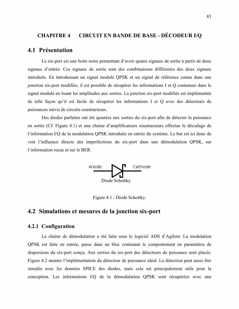
83
CHAPITRE 4 CIRCUIT EN BANDE DE BASE - DÉCODEUR I/Q
4.1 Présentation
Le six-port est une boite noire permettant d’avoir quatre signaux de sortie à partir de deux
signaux d’entrée. Ces signaux de sortie sont des combinaisons différentes des deux signaux
introduits. En introduisant un signal modulé QPSK et un signal de référence connu dans une
jonction six-port modifiée, il est possible de récupérer les informations I et Q contenues dans le
signal modulé en lisant les amplitudes aux sorties. La jonction six-port modifiée est implémentée
de telle façon qu’il est facile de récupérer les informations I et Q avec des détecteurs de
puissances suivis de circuits soustracteurs.
Des diodes parfaites ont été ajoutées aux sorties du six-port afin de détecter la puissance
en sortie (Cf. Figure 4.1) et une chaine d’amplificateurs soustracteurs effectue le décodage de
l’information I/Q de la modulation QPSK introduite en entrée du système. Le but est ici donc de
voir l’influence directe des imperfections du six-port dans une démodulation QPSK, sur
l’information reçue et sur le BER.
Figure 4.1 : Diode Schottky.
4.2 Simulations et mesures de la jonction six-port
4.2.1 Configuration
La chaine de démodulation a été faite sous le logiciel ADS d’Agilent. La modulation
QPSK est faite en entrée, passe dans un bloc contenant le comportement en paramètres de
dispersions du six-port conçu. Aux sorties du six-port des détecteurs de puissance sont placés.
Figure 4.2 montre l’implémentation du détecteur de puissance idéal. La détection peut aussi être
simulée avec les données SPICE des diodes, mais cela est principalement utile pour la
conception. Les informations I/Q de la démodulation QPSK sont récupérées avec une
Diode Schottky
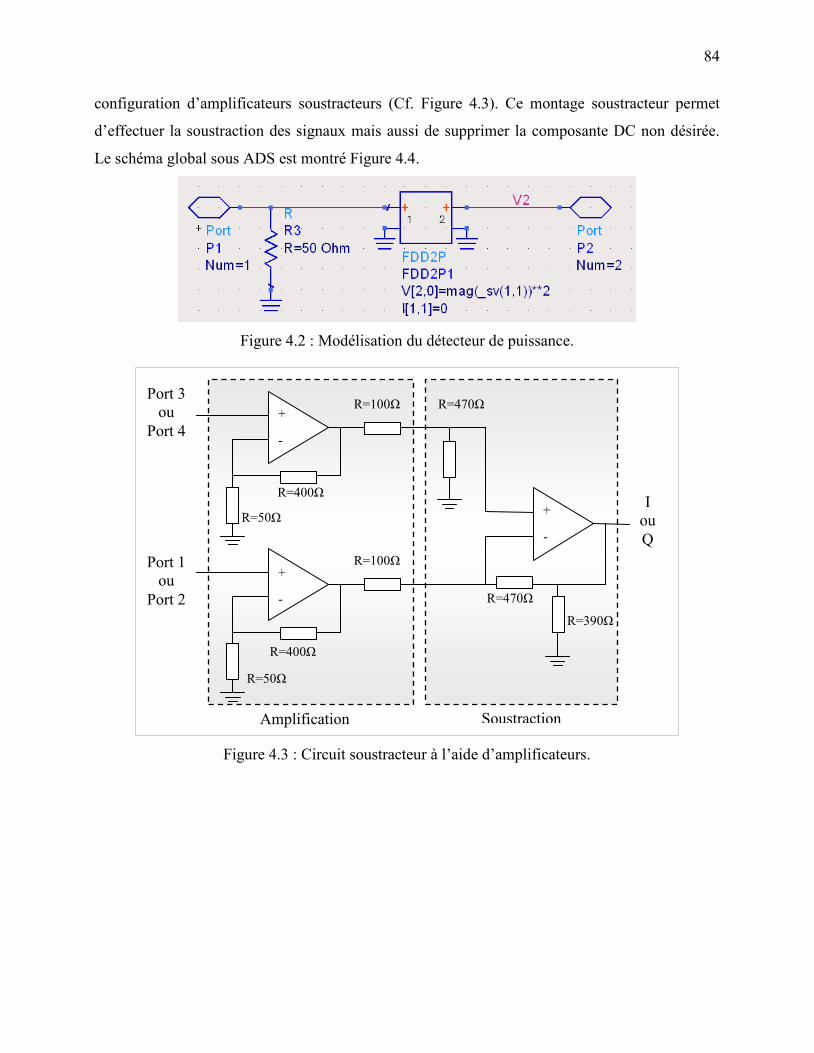
84
configuration d’amplificateurs soustracteurs (Cf. Figure 4.3). Ce montage soustracteur permet
d’effectuer la soustraction des signaux mais aussi de supprimer la composante DC non désirée.
Le schéma global sous ADS est montré Figure 4.4.
Figure 4.2 : Modélisation du détecteur de puissance.
Figure 4.3 : Circuit soustracteur à l’aide d’amplificateurs.
+
-
+
-
+
-
Port 3 ou
Port 4
I ou Q
Port 1 ou
Port 2
Amplification Soustraction
R=50Ω
R=400Ω
R=50Ω
R=400Ω
R=100Ω
R=100Ω
R=470Ω
R=470Ω
R=390Ω

85
Figure 4.4 : Schéma de la simulation ADS de la conversion directe.
4.2.2 Résultats
Afin de pouvoir voir l’influence du démodulateur six-port dans le système de
démodulation, les signaux I/Q démodulés de sortie sont comparés avec ceux injectés en entrée
[Tatu (2004)]. La propagation du signal est simulée en utilisant le composant LOS_link d’ADS
qui représente la transmission d’un signal en se basant sur le modèle établi par Friis [Stutzman et
Thiele (1998)]. La simulation représente un système avec une vitesse de modulation QPSK de
100 Mb/s (50 Mb/s par canal), et des antennes de gain 15 dBi situées à une distance de 5 mètres.
Pour donner un ordre de grandeur, un débit de 54Mb/s est nécessaire pour la lecture de film blu-
ray haute définition [Blu-ray.com]. La fréquence de fonctionnement considérée est 60 GHz et la
phase de l’oscillateur local est supposée parfaitement stable (oscillateur verrouillé en phase).
Figure 4.5 représente les signaux d’entrée et de sortie dans la plage de 0 à 1 µs. Phase In est la
phase du signal modulé QPSK d’entrée Iout/Qout et Iin/Qin sont respectivement des signaux I/Q
de sortie et d’entrée. On voit que le six-port apporte peu de distorsion dans les signaux récupérés.
Une légère variation d’amplitude de voltage peut être remarquée (notamment sur Iout). Celle-ci
est due aux légères variations de couplage du six-port. La démodulation est donc effectuée
correctement.

86
Figure 4.5 : Signaux d’entrée et sortie.
Figure 4.6. illustre le spectre du signal d’entrée modulé QPSK. On peut noter la largeur du
spectre qui correspond à un signal de 100 Mb/s.
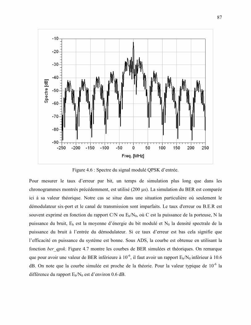
87
Figure 4.6 : Spectre du signal modulé QPSK d’entrée.
Pour mesurer le taux d’erreur par bit, un temps de simulation plus long que dans les
chronogrammes montrés précédemment, est utilisé (200 µs). La simulation du BER est comparée
ici à sa valeur théorique. Notre cas se situe dans une situation particulière où seulement le
démodulateur six-port et le canal de transmission sont imparfaits. Le taux d'erreur ou B.E.R est
souvent exprimé en fonction du rapport C/N ou Eb/N0, où C est la puissance de la porteuse, N la
puissance du bruit, Eb est la moyenne d’énergie du bit modulé et N0 la densité spectrale de la
puissance du bruit à l’entrée du démodulateur. Si ce taux d’erreur est bas cela signifie que
l’efficacité en puissance du système est bonne. Sous ADS, la courbe est obtenue en utilisant la
fonction ber_qpsk. Figure 4.7 montre les courbes de BER simulées et théoriques. On remarque
que pour avoir une valeur de BER inférieure à 10-6, il faut avoir un rapport Eb/N0 inférieur à 10.6
dB. On note que la courbe simulée est proche de la théorie. Pour la valeur typique de 10-6 la
différence du rapport Eb/N0 est d’environ 0.6 dB.
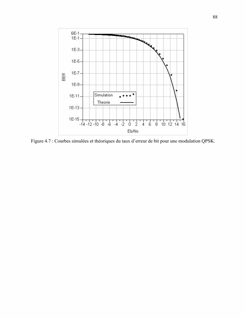
88
Figure 4.7 : Courbes simulées et théoriques du taux d’erreur de bit pour une modulation QPSK.
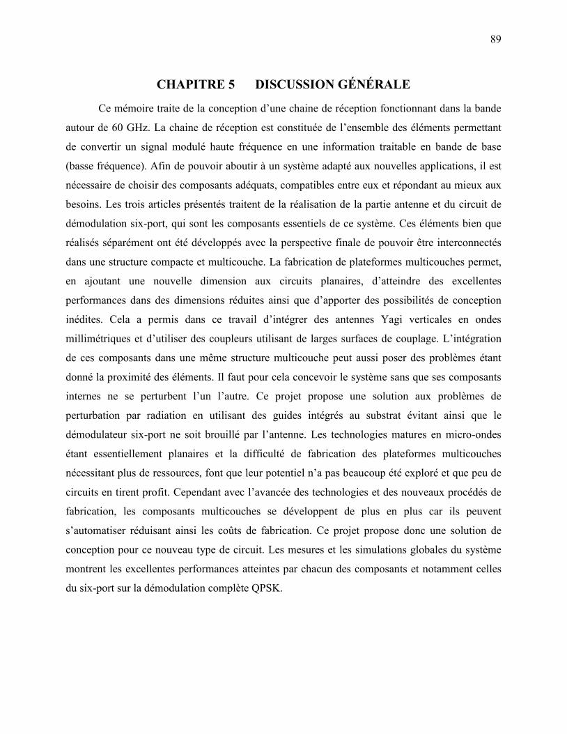
89
CHAPITRE 5 DISCUSSION GÉNÉRALE
Ce mémoire traite de la conception d’une chaine de réception fonctionnant dans la bande
autour de 60 GHz. La chaine de réception est constituée de l’ensemble des éléments permettant
de convertir un signal modulé haute fréquence en une information traitable en bande de base
(basse fréquence). Afin de pouvoir aboutir à un système adapté aux nouvelles applications, il est
nécessaire de choisir des composants adéquats, compatibles entre eux et répondant au mieux aux
besoins. Les trois articles présentés traitent de la réalisation de la partie antenne et du circuit de
démodulation six-port, qui sont les composants essentiels de ce système. Ces éléments bien que
réalisés séparément ont été développés avec la perspective finale de pouvoir être interconnectés
dans une structure compacte et multicouche. La fabrication de plateformes multicouches permet,
en ajoutant une nouvelle dimension aux circuits planaires, d’atteindre des excellentes
performances dans des dimensions réduites ainsi que d’apporter des possibilités de conception
inédites. Cela a permis dans ce travail d’intégrer des antennes Yagi verticales en ondes
millimétriques et d’utiliser des coupleurs utilisant de larges surfaces de couplage. L’intégration
de ces composants dans une même structure multicouche peut aussi poser des problèmes étant
donné la proximité des éléments. Il faut pour cela concevoir le système sans que ses composants
internes ne se perturbent l’un l’autre. Ce projet propose une solution aux problèmes de
perturbation par radiation en utilisant des guides intégrés au substrat évitant ainsi que le
démodulateur six-port ne soit brouillé par l’antenne. Les technologies matures en micro-ondes
étant essentiellement planaires et la difficulté de fabrication des plateformes multicouches
nécessitant plus de ressources, font que leur potentiel n’a pas beaucoup été exploré et que peu de
circuits en tirent profit. Cependant avec l’avancée des technologies et des nouveaux procédés de
fabrication, les composants multicouches se développent de plus en plus car ils peuvent
s’automatiser réduisant ainsi les coûts de fabrication. Ce projet propose donc une solution de
conception pour ce nouveau type de circuit. Les mesures et les simulations globales du système
montrent les excellentes performances atteintes par chacun des composants et notamment celles
du six-port sur la démodulation complète QPSK.

90
CONCLUSION ET TRAVAUX FUTURS
Ce mémoire présente l’analyse, la conception et la réalisation d’une chaine de réception
en ondes millimétriques multicouche. Les éléments principaux constituant le système de
réception ont été analysés. La rédaction de cette thèse est articulée autour de trois articles dont un
a déjà été publié dans IEEE Transaction on Antennas & Propagation et deux ont été soumis dans
IEEE Transaction on Antennas & Propagation et IEEE MTT-S Transaction. La première partie
traite de la conception d’antenne. Deux premiers prototypes fonctionnant à 5.8 GHz ont été
conçus et caractérisés. Les mesures des paramètres de dispersion montrent une bonne largeur de
bande (une largeur de bande de 15% peut être atteinte). Les diagrammes de rayonnement mesurés
correspondent aux simulations. Les deux conceptions ont un gain maximal mesuré de 11 et 10
dBi. L’analyse des paramètres de conception a été effectuée pour identifier les paramètres
critiques.
Basé sur ces structures, la deuxième partie présente le design d’antennes à 60 GHz
permettant d’ôter les espaces d’air entre les différentes couches présents en basses fréquences.
Une antenne élément à 60 GHz ainsi que de deux antennes réseaux 4x4 alimentées en GIS sont
présentées. Le premier réseau a une bande passante de 7% avec un gain mesuré de 18 dBi. Le
deuxième réseau utilise une orientation individuelle des éléments pour permettre une réduction
des lobes secondaires tout en gardant un bon gain.
Dans la troisième partie, la conception du circuit de démodulation six-port est présentée.
Il utilise la technologie des GIS afin de pouvoir le connecter sans transitions aux réseaux
d’antennes créés précédemment. Ce six-port est réalisé sur deux couches afin d’avoir une large
surface de couplage, possède six accès exactement et utilise un nouveau déphaseur double stub
plan-H dont l’analyse mathématique a été faite. Le six-port fabriqué montre une erreur de
couplage et phase de respectivement −6.7 dB ±0.7 et 10°, sur la bande 57-65 GHz (20 % de
bande passante à 60 GHz). Cette structure possède les avantages d’être à la fois compacte, peu
radiative, facile à fabriquer et intégrable au plus près de l’antenne.
La quatrième partie traite du système en bande de base afin de récupérer les données du
signal source encodé en QPSK. Les performances du six-port dans le système complet sont
testées et montrent que celui-ci répond aux exigences du système de démodulation avec un BER
proche de la valeur théorique.

91
En conclusion, ces trois parties peuvent s’intégrer l’une par rapport à l’autre, pour pouvoir
obtenir un système de réception à la fois petit et performant. La conception de tous ces éléments
au sein d’un même bloc reste à réaliser car elle n’a pas été faite faute de temps. Ce design montre
beaucoup de potentiel pour des applications d’imageries à 94 GHz ou en térahertz. L’imagerie
térahertz (ou sous-millimétrique) est un domaine avec de nombreuses ramifications pouvant avoir
des impacts dans le domaine aéronautique ou médical. Elle traite des fréquences dans la bande
entre 100 GHz et plus de 5 THz. Parmi les antennes térahertz, on peut citer l’utilisation de
spirales, antennes log-périodiques, dipôles, antennes à fentes, etc. Cependant ces structures
posent des problèmes de fabrication (e.g. spirale) ou n’ont pas des gains intrinsèquement élevés.
Une autre antenne utilisée est l’antenne cornet mais dont les dimensions élevées ne permettent
pas un balayage rapproché car dans le champ proche (de l’ordre du mètre) et dont la fabrication
ne peut être complètement automatisée. En reprenant les principes des réseaux d’antennes Yagi-
Uda présentés ici, des antennes ayant les avantages suivants pourront être crées en fréquences
sous-millimétriques :
• Empreinte petite du fait de sa conception, permettant d’avoir un champ lointain de
quelques centimètres et donc de pouvoir balayer de très près.
• Un gain très élevé afin d’avoir une résolution d’image maximale ou une augmentation de
la portée.
• Pouvoir contrôler les lobes secondaires, la largeur de bande ou placer des zéros dans le
diagramme de rayonnement en adaptant l’orientation individuelle des éléments.
Parmi les améliorations futures à apporter à cette conception, on peut citer l’implantation
d’une polarisation circulaire (afin de pouvoir capter plus d’information sur une image),
l’utilisation d’un réseau afin de réaliser un balayage contrôlé électriquement plus rapide que le
balayage mécanique, ou sa fabrication utilisant les nouveaux procédés en technologie film-épais
photosensible (Fodel ® - [Aftanasar et al. (2001), Stephens et al. (2006)]) qui permettent d’avoir
des coûts de fabrication très bas, couvrant une bande allant de 100 GHz à 1 THz. L’amélioration
des performances du réseau d’antennes pourra être effectuée avec une étude approfondie sur les
phénomènes de couplages entre antennes et sur les possibilités de formation de faisceau
(beamforming).
Cette structure montre un grand nombre d’atouts grâce à sa flexibilité et sa conception
adaptée aux hautes fréquences. Une déclaration d’invention sur celle-ci est déposée dans le cadre

92
du processus de valorisation mis en place par l’École Polytechnique de Montréal et Univalor, en
raison des futures applications industrielles possibles notamment dans le domaine de l’imagerie.
Ce type d’antenne est d’hors et déjà testé pour des fabrications à 100 GHz.
93
RÉFÉRENCES
Aftanasar M.S., Young P.R., Robertson I.D., Minalgiene J., et Lucyszyn S., “Photoimageable
thick-film millimetre-wave metal-pipe rectangular waveguides,” Electronic Letters, vol.
37, no. 18, pp. 1122-1123, 2001.
Bilik V., Bezek J., et Raffaj V., “Three-probe X-band waveguide six-port reflectometer,”
Elektrotechnicky casopis, vol. 41, no. 5, p. 329-342, 1990.
Bilík, V., “Six-port Measurement Technique: Principles, Impact, Applications,” Mar. 2008,
http://www.s-team.sk/download/SixPortTechnique.pdf
Blu-ray.com, http://www.blu-ray.com/faq, 2010
Bosco B., Franson S., Emrick R., Rockwell S., et Holmes J., “A 60 GHz Transceiver with
Multi-Gigabit Data Rate Capability,” IEEE Radio and Wireless Conference, pp. 135-138,
2004.
Cohn S.B., et Weinhouse N.P. “An Automatic Microwave Phase Measurement System,”
Microwave Journal, Fev. 1964.
Cronson H.M. et Susman L., “A Dual Six-Port Automatic Network Analyzer,” IEEE Trans.
Microwave Theory and Tech., vol. MTT-29, no. 4, pp. 372-378, Avr. 1981.
Deslandes D.et Wu K., “Accurate Modeling, Wave Mechanisms, and Design Considerations
of Substrate Integrated Waveguide,” IEEE Trans. Microwave Theory Tech., vol. 54, pp.
2516-2526, Juin 2006.
Engen G. F., “The six-port reflectometer: an alternative network analyzer,” IEEE Trans.
Microwave Theory Tech., vol. MTT-25, no. 12, p. 1075-1080, Dec. 1977.
Fusco V., et Wang C., “V-band 57–65 GHz receiver,” IET Microwaves Antennas &
Propagation, vol. 4, Iss. 1, pp. 1–7, Jan. 2010.
Gunnarsson S., Karnfelt C., Zirath H., Kozhuharov R., Kuylenstierna D., Alping A., et Fager
C., “Highly integrated 60 GHz transmitter and receiver MMICs in a GaAs pHEMT
technology,” IEEE J. Solid-State Circuits, vol. 40, no. 11, pp. 2174–2186, Nov. 2005.
Hoer C. A., “A network analyzer incorporating two six-port reflectometers,” IEEE Trans.
Microwave Theory Tech., vol. MTT-25, no. 12, p. 1070-1074, Dec. 1977.
IEEE 802.11 Very High Throughput Study Group. Available:
http://www.ieee802.org/11/Reports/vht update.htm

94
IEEE 802.15 WPAN Millimeter-wave Alternative PHY Task Group 3c (TG3c). Available:
http://www.ieee802.org.org/15/pub/TG3c.html
Stephens D., Young P.R., et Robertson I.D., “Millimeter-Wave Substrate Integrated
Waveguides and Filters in Photoimageable Thick-Film Technology”, IEEE Transactions
on Microwave Theory and Techniques, vol. 53, no. 12, pp. 3832-3838, 2005.
Stutzman W.L. et Thiele G. A., Antenna Theory and Design, Second Edition, John Wiley and
Sons, 1998.
Sum C.S, Lan Z, Rahman M. A., Wang J., Baykas T., Funada R., Harada H. et Kato S., “A
Multi-Gbps Millimeter-wave WPAN System based on STDMA with Heuristic Scheduling,”
IEEE Global Communication Conference (Globecom) 2009, Honolulu, USA 30
Novembre – 4 Decembre 2009.
Sun Y., Glisic S., Herzel F., Schmalz K., Grass E., Winkler W., et Kraemer R., “An
integrated 60 GHz transceiver front-end for OFDM in SiGe: BiCMOS,” Wireless World
Research Forum 16, Shanghai, China, Avr. 2006.
Tatu S. O., “Nouveau Récepteur six-port en ondes millimétriques,” 2004.
Uda S. “Radiotelegraphy and radiotelephony on half-meter waves,” Proc. IRE, vol. 18, pp.
1047–1063, 1930.
Wikipedia.fr, http://fr.wikipedia.org/wiki/Yagi, 2010
Yagi H., “Beam transmission of ultra short waves,” Proc. IRE, vol. 16, pp. 715–741, Juin
1928.
Zborowska J., Thao N., Morawski T., et Sypniewski M., “A new concept of threeport
microwave reflectometer with AM/PM switched modulator, ” Proc. Miteko 1989,
Pardubice, 1989