Embed Size (px)
Citation preview
Transistor and Circuit Design for 100-200 GHz ICsM. Rodwell, Z. Griffith, D. Scott, Y. Wei, Y.
Dong, V. Paidi, M. Dahlström, N. Parthasarathy, C. Kadow, ECE Department, University of
California, Santa Barbara, 93106, USA, [email protected]
M. Urteaga , R. Pierson, P. Rowell, B. Brar, Rockwell
Scientific Company, Thousand Oaks, CA 91360,
USA
S. Lee, N. Nguyen, and C. Nguyen, Global Communication Semiconductors, Torrance, CA,
Abstract — Compared to SiGe, InP HBTs offer superior
electron transport but inferior scaling and parasitic reduction. Figures of merit for mixed-signal ICs are developed and HBT scaling laws for improved circuit speed are introduced. Device and circuit results are summarized, including 390 GHz fτ / 500 GHz fmax DHBTs, 174 GHz amplifiers, and 150 GHz static frequency dividers. To compete with 100 nm SiGe processes, InP must be similarly scaled, and high process yields are imperative. We describe several process modules in development, including emitter regrowth, emitter-base dielectric sidewall processes, and a collector pedestal implant process.
I. INTRODUCTION
Despite formidable progress in CMOS, bipolar transistors are competitive due to the larger breakdown voltages obtainable and the larger lithographic feature sizes required for a transistor of a specified bandwidth. SiGe HBTs have demonstrated simultaneous > 300 GHz
and and 96 GHz static dividers, while InP DHBTs have obtained ~400 GHz and ~500 GHz , > 150 GHz static dividers, and 176 GHz power amplifiers. Compared to SiGe, InP HBTs have ~3.5:1 better collector electron velocity and ~10:1 better base electron diffusivity. Consequently, given the same junction dimensions, an InP HBT would have ~3:1 greater bandwidth than a SiGe HBT. Today, SiGe HBTs are fabricated with much narrower junctions and much smaller extrinsic parasitics. Consequently, the two technologies today have comparable bandwidth, while SiGe offers much higher integration scales. Continued progress with InP HBTs therefore requires close attention to scaling laws and scaling limits. Requirements placed upon transistor design for wideband circuits must be clearly understood. Fabrication processes must provide high yield at 100 nm scaling.
τf maxfτf maxf
II. HBT PERFORMANCE METRICS
τf
clock,
gate =
LV
and are of limited value in predicting the speed of logic, mixed-signal, or optical transmission ICs. As representative case, the maximum clock frequency
of an ECL master-slave latch1 is ; Table 1 gives the delay
coefficients and the components of T for an HBT with target 260 GHz . In terms of resistances, 82% of arises from the load resistance . High current density is essential. Since the logic voltage swing
must be at least , increased current density much be accompanied by reduced emitter resistance, so as to maintain low . In terms of
capacitances, 58% of arises from the depletion capacitances
maxf
f clock,2a
gateT
maxfT /1
∆
jiij CRaΣ=max
ij
maxclock,f
(4 kT +
gate
V∆ cL I/
)EEX IR
∆ LV
gateTjeCC + , and only 18% with fτ , even
jeC cbxC C L
EW I
exR
cb.. cbi Ef VI ∆/τ
LEW VI ∆/τ
EL IV /∆ 1 6 6 1 1
EqIkT / 0.5 1 1 0.5 0
EXR -0.3 0.5 0.5 0.5 0
bbR 0.5 0 1 0.5 0
.. jeC cbxC cbiC LEf VI ∆/τ
LV∆/τ sum EL IV /∆ 11% 16% 22% 49%
EL IV /∆ 15% 18% 33%
EqIkT/ 1% 1%
EXR -1% 1% 0%
bbR 5% 3% 7% 15%
sum 16% 16% 25% 24% 18% 100%
42%
Table. 1: (top) Delay coefficients a ij for an ECL M-S latch, where jiijgate CRafT Σ== maxclock,2/1
je
cτ+
LV∆
∆
. (bottom) Proportions of for a 300-nm scaling-generation HBT with target 260 GHz
clock rate. C is the emitter depletion capacitance, and the extrinsic and intrinsic collector base capacitances,
the forward transit time, the wiring delay, the emitter current, the logic voltage swing, and and
the parasitic emitter and base resistances. influences indirectly through increased .
gateT
cbiC
fτ =
bbR
clock,f
cbxC
exRbτ
max
Wτ
LV
EI
Parameter Gen. 1 Gen. 2 Gen. 3 MS-DFF speed 60 GHz 121 GHz 260 GHz
Emitter Width 1 µm 0.8 µm 0.3 µm Parasitic Resistivity 50 Ω-µm2 20 Ω-µm2 5 Ω-µm2
Base Thickness 400Å 400Å 300 Å Doping 5 1019 /cm2 7 1019 /cm2 7 1019 /cm2 Sheet resistance 750 Ω 700 Ω 700 Ω Contact resistance 150 Ω-µm2 20 Ω-µm2 20 Ω-µm2
Collector Width 3 µm 1.6 µm 0.7 µm Collector Thickness 3000 Å 2000 Å 1000 Å Current Density 1 mA/µm2 2.3 mA/µm2 12 mA/µm2 Acollector/Aemitter 4.55 2.6 2.9
τf 170 GHz 248 GHz 570 GHz
maxf 170 GHz 411 GHz 680 GHz
EE LI / 1 mA/µm 1.9 mA/µm 3.7 mA/µm
fτ 0.67 ps 0.50 ps 0.22 ps
ccb IC / 1.7 ps/V 0.62 ps/V 0.26 ps/V
ccb IVC /logic∆ 0.5 ps 0.19 ps 0.09 ps
)//( logic cbb IVR ∆ 0.8 0.68 0.99
)/( logic Cje IVC ∆ 1.7 ps 0.72 ps 0.15 ps
)//( logic cex IVR ∆ 0.1 0.15 0.17
Table. 2: Technology roadmaps for 40, 80, and 160 Gb/s ICs. Master-slave latch delay includes 10% interconnect delay.
given the assumed transistor design having small ratios. IC /
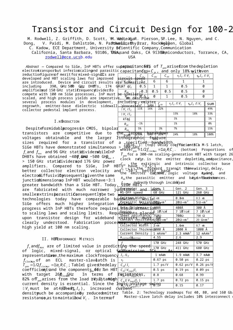
Figure 1: RF gains; 600-nm emitter-width InP mesa DHBT.
nFor logic and mixed-signal ICs, low C and charging times are critical, necessitating very
high current density, minimal excess collector junction area, and very low emitter access resistance. Transit delay plays a smaller role; at a given scaling generation, an HBT can be designed for highest feasible while sacrificing both and logic speed. Such transistors, regularly reported in the literature, have limited value.
ELcb IV /∆
τf
ELje IVC /∆
maxf
II. SCALING: LAWS, LIMITATIONS, & ROADMAPS
Consider scaling laws 1. For a 2:1 speed increase in all circuits, all device capacitances and transit delays must be reduced 2:1 while maintaining constant , , and all parasitic resistances. This is accomplished by thinning the collector depletion layer 2:1, thinning the base
CI mg
2 :1, reducing the emitter and collector junction areas 4:1 and widths ~4:1, reducing the emitter resistance per unit area 4:1, and increasing the current density 4:1. Thinning the collector 2:1 increases the collector capacitance per unit area 2:1 but increases the Kirk-effect-limited current density 4:1; C is thus reduced 2:1. If the base Ohmic contacts lie above the collector junction, their width must be reduced 2:1, necessitating a ~4:1 reduction in contact resistivity; if the contacts do not lie above the junction, their resistivity can remain unscaled.
Ccb I/
-90
-80
-70
-60
-50
-40
-30
-20
-10
0.0 15.0 30.0 45.0 60.0 75.0
Out
put P
ower
(dB
m)
frequency (GHz)
Emitter and base contact resistivity, thermal resistance, and fabrication yield are the key barriers to scaling. Typically the collector-base junction lies below the full width of the base contact, hence narrow collector junctions demand narrow base contacts. This demands low base contact resistance (~15 ), low base metal sheet resistance, and tight alignment tolerances or self-aligned processes. Emitter contact resistivity is critical, as very low values (~5 ) are required for 200 GHz clock speed. Current density must be very high (10-15 mA/ ) hence thermal resistance also must be low2, . Indeed, because current density increases in proportion to the bandwidth squared, maximum reliable power density is a more serious practical limit to applied voltage than the breakdown voltage V . Table 2 shows a scaling roadmap.
2mµ−Ω
2mµ−Ω
CEEVJ
2mµm K µ⋅
br
mW/5 2<
ceo,
Figure 2: UCSB-built 142-GHz static divider using the HBT of figure 1; circuit diagram, photograph, and output spectrum
-90
-80
-70
-60
-50
-40
-30
-20
-10
0.00 19.00 38.00 57.00 76.00
Out
put P
ower
(dB
m)
frequency (GHz)
0
5
10
15
20
25
30
35
109 1010 1011 1012
Gai
ns (d
B)
Frequency (Hz)
ft = 391 GHz, f
max = 505 GHz
U
H21
Ic = 13.2 mA
Ajbe
= 0.6 x 4.25 um2
Je = 5.17 mA/um2, V
cb= 0.6 V
200
300
400
500
1 2 3 4 5 6
GH
z
Je (mA/um2)
ft
fmax
Vcb
= 0.6 V
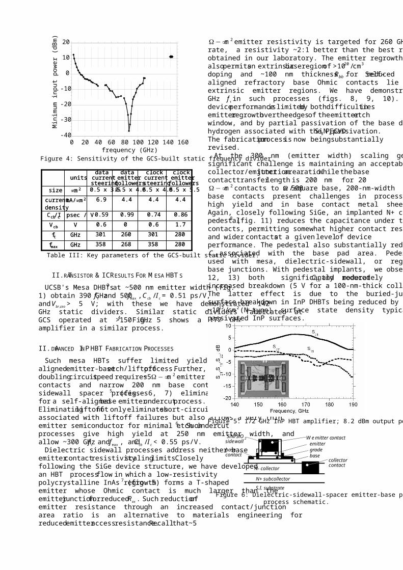
Figure 3: Output spectrum of GCS-built static divider at 150 GHz clock frequency.
-40
-30
-20
-10
0
10
20
0 20 40 60 80 100 120 140 160
Min
imum
inpu
t pow
er (d
Bm
)
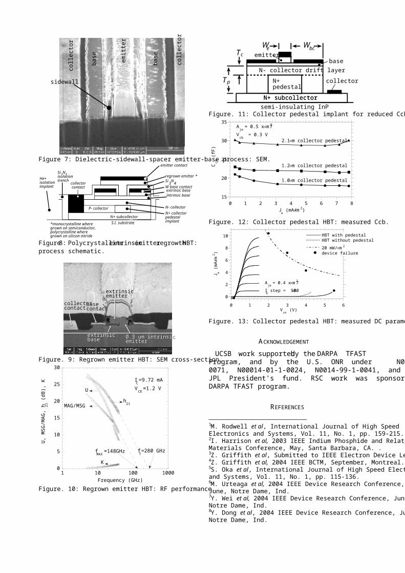
frequency (GHz) Figure 4: Sensitivity of the GCS-built static frequency divider.
0.860.740.990.59psec / VCcb/Ic
358
301
0.6
4.4
0.5 x 4.5
clock current steering
GHz
GHz
V
mA/µm2
µm2
units
280268358fmax
280260301ft
1.700.6Vcb
4.44.46.9currentdensity
0.5 x 5.50.5 x 4.50.5 x 3.5size
clock emitter
followers
data emitter
followers
data current steering
0.860.740.990.59psec / VCcb/Ic
358
301
0.6
4.4
0.5 x 4.5
clock current steering
GHz
GHz
V
mA/µm2
µm2
units
280268358fmax
280260301ft
1.700.6Vcb
4.44.46.9currentdensity
0.5 x 5.50.5 x 4.50.5 x 3.5size
clock emitter
followers
data emitter
followers
data current steering
Table III: Key parameters of the GCS-built static divider.
II. TRANSISTOR & IC RESULTS FOR MESA HBTS
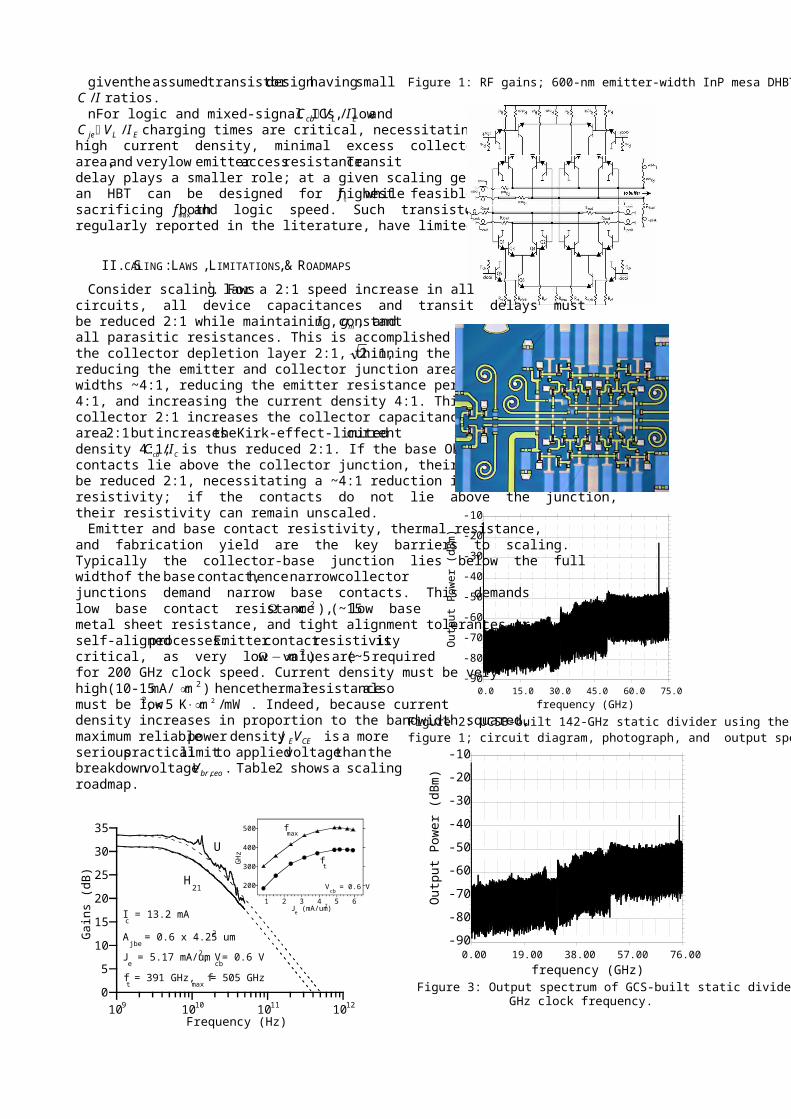
UCSB's Mesa DHBTs 3 at ~500 nm emitter width (fig. 1) obtain 390 GHz and 500 , = 0.51 ps/V, and > 5 V; with these we have demonstrated 142 GHz static dividers. Similar static dividers fabricated at GCS operated at >150 GHz4. Fig. 5 shows a 172 GHz amplifier in a similar process.
τf maxf ccb IC /ceobrV ,
II. ADVANCED INP HBT FABRICATION PROCESSES
Such mesa HBTs suffer limited yield from the self-aligned emitter-base etch/liftoff process. Further, doubling circuit speed requires ~5 emitter contacts and narrow 200 nm base contacts. Dielectric sidewall spacer processes5 (fig. 6, 7) eliminate the need for a self-aligned base emitter undercut process. Eliminating liftoff not only eliminates short-circuits associated with liftoff failures but also allows a very thin emitter semiconductor for minimal etch undercut 6. Such processes give high yield at 250 nm emitter width, and allow ~300 GHz and , and C < 0.55 ps/V.
2mµ−Ω
cτf maxf cb I/Dielectric sidewall processes address neither base nor
emitter contact resistivity scaling limits. Closely following the SiGe device structure, we have developed an HBT process flow in which a low-resistivity polycrystalline InAs regrowth 7 (fig. 5) forms a T-shaped emitter whose Ohmic contact is much larger than the emitter junction for reduced . Such reduction of emitter resistance through an increased contact/junction area ratio is an alternative to materials engineering for reduced emitter access resistance. Recall that ~5
emitter resistivity is targeted for 260 GHz clock rate, a resistivity ~2:1 better than the best results thus far obtained in our laboratory. The emitter regrowth process also permits an extrinsic base region of >10 doping and ~100 nm thickness for reduced . Self-aligned refractory base Ohmic contacts lie under the extrinsic emitter regions. We have demonstrated 280 GHz in such processes (figs. 8, 9, 10). Presently, device performance is limited by both difficulties in emitter regrowth over the edges of the emitter etch window, and by partial passivation of the base doping by hydrogen associated with the PECVD Si passivation. The fabrication process is now being substantially revised.
exR
2mµ−Ω
τf
2mµ−Ω
320 cm/bbR
43N
cbC
12 cm/
cbC
se
mitter c
c
o
colo
ntact
lectorntact
emitterbasecontact
SiN/side
ade
At the 300 nm (emitter width) scaling generation, a significant challenge is maintaining an acceptably small collector/emitter junction area ratio. While the base contact transfer length is 200 nm for 20
contacts to a 500 Ω /square base, 200-nm-width base contacts present challenges in process design for high yield and in base contact metal sheet resistance. Again, closely following SiGe, an implanted N+ collector pedestal8 (fig. 11) reduces the capacitance under the base contacts, permitting somewhat higher contact resistivities and wider contacts at a given level of device performance. The pedestal also substantially reduces the
associated with the base pad area. Pedestals can be used with mesa, dielectric-sidewall, or regrown emitter-base junctions. With pedestal implants, we observe (figs. 12, 13) both significantly reduced and moderately increased breakdown (5 V for a 100-nm-thick collector). The latter effect is due to the buried-junction device, surface breakdown in InP DHBTs being reduced by the ~10 (N-type) surface state density typical of ill-passivated InP surfaces.
2
Figure 5: 172 GHz InP HBT amplifier; 8.2 dBm output power
N- collector
N+ subcollector
S.I. substrate
W e
ba
SiO2wall
gr
Figure 6: Dielectric-sidewall-spacer emitter-base process; process schematic.
emitter
base
base
collector
collector
sidewall
Figure 7: Dielectric-sidewall-spacer emitter-base process: SEM.
*monocrystalline wheregrown on semiconductor,polycrystalline wheregrown on silicon nitride
N- collector
N+ subcollectorS.I. substrate
intrinsic base extrinsic baseW base contactSi3N4
regrown emitter *
emitter contact
collector contact
N+ collectorpedestalimplant
P- collector
Si3N4isolationtrenchHe+
isolationimplant
Figure 8: Polycrystalline extrinsic emitter regrowth HBT: process schematic.
0.3 um intrinsicemitter0.3 um intrinsicemitter
extrinsicbaseextrinsicbase
base contactbase contact
collector contactcollector contact
extrinsic emitterextrinsic emitter
Figure. 9: Regrown emitter HBT: SEM cross-section.
0
5
10
15
20
25
30
1 10 100 1000
IC=9.72 mA
VCE
=1.2 V
U, M
SG
/MA
G, h
21 (d
B),
K
Frequency (GHz)
U
h21MAG/MSG
K
fT=280 GHzf
MAX=148GHz
Figure. 10: Regrown emitter HBT: RF performance.
emitter
N+pedestal
semi-insulating InPN+ subcollector
N- collector drift layerbase
collector
cT
pT N+pedestal
N+ subcollector
bcWeW
Figure. 11: Collector pedestal implant for reduced Ccb.
15
20
25
30
35
0 1 2 3 4 5 6 7 8
Ccb
(fF)
Je (mA/µm2)
Aje = 0.5 x 7 µm2
Vcb
= 0.3 V2.1 µm collector pedestal
1.2 µm collector pedestal
1.0 µm collector pedestal
Figure. 12: Collector pedestal HBT: measured Ccb.
0
2
4
6
8
10
0 1 2 3 4 5 6
J e (mA
/µm
2 )
Vce
(V)
Aje = 0.4 x 7 µm2
Ib step = 500 µA
HBT with pedestalHBT without pedestal
20 mW/µm2 device failure
Figure. 13: Collector pedestal HBT: measured DC parameters
ACKNOWLEDGEMENT
UCSB work supported by the DARPA TFAST Program, and by the U.S. ONR under N00014-04-1-0071, N00014-01-1-0024, N0014-99-1-0041, and by a JPL President's fund. RSC work was sponsored by the DARPA TFAST program.
REFERENCES
1M. Rodwell et al, International Journal of High Speed Electronics and Systems, Vol. 11, No. 1, pp. 159-215. 2I. Harrison et al, 2003 IEEE Indium Phosphide and Related Materials Conference, May, Santa Barbara, CA. . 3Z. Griffith et al, Submitted to IEEE Electron Device Letters 4Z. Griffith et al, 2004 IEEE BCTM, September, Montreal. 5S. Oka et al, International Journal of High Speed Electronics and Systems, Vol. 11, No. 1, pp. 115-136. 6M. Urteaga et al, 2004 IEEE Device Research Conference, June, Notre Dame, Ind. 7Y. Wei et al, 2004 IEEE Device Research Conference, June, Notre Dame, Ind. 8Y. Dong et al, 2004 IEEE Device Research Conference, June, Notre Dame, Ind.