Embed Size (px)
Citation preview
C. R. Physique 3 (2002) 89–102
Électromagnétisme, optique/Electromagnetism, optics(Solides, fluides : propriétés électroniques et optiques/Solids, fluids: electronic and optical properties)
DO
SS
IER
MICROCAVITÉS ET CRISTAUX PHOTONIQUES
MICROCAVITIES AND PHOTONIC CRYSTALS
Two-dimensional photonic crystals:new feasible confined optical systemsHenri Benisty, Maxime Rattier, Ségolène Olivier
Laboratoire de physique de la matière condensée, UMR 7643 du CNRS, École polytechnique,91128 Palaiseau cedex, France
Received and accepted 23 November 2001
Note presented by Guy Laval.
Abstract After a brief review of the basic properties of ideal two-dimensional photonic crystals,we describe the recent advances that have led to them being considered candidates inrealistic, feasible optoelectronic systems that take advantage of their powerful light controlcapability. Two main fields of applications are integrated optics and microstructuredfibres. We focus on the former one, closer to the genuine photonic gap concept. Weillustrate through a number of optical elements – simple crystals, guides and cavities –the peculiarities of confinement by such systems. To cite this article: H. Benisty et al.,C. R. Physique 3 (2002) 89–102. 2002 Académie des sciences/Éditions scientifiques etmédicales Elsevier SAS
photonic crystal / photonic bandgap / integrated optics / optical fibre / guide / cavity
Cristaux photoniques bi-dimensionnels : des systèmes optiquesconfinés nouveaux et faisables
Résumé Après un bref passage en revue des propriétés de base des cristaux photoniques bi-dimensionnels idéaux, nous décrivons les avancées récentes qui montrent commentmettre à profit leurs puissantes capacités de contrôle de la lumière dans des systèmesoptoélectroniques faisables. Deux des domaines d’application principaux sont l’optiqueintégrée et les fibres microstructurées. Nous nous concentrons sur le premier, plus prochedu concept d’origine de bande interdite photonique. Nous illustrons au travers de diverséléments optiques – simple cristaux, guides, cavités – les particularités du confinementdans ces systèmes. Pour citer cet article : H. Benisty et al., C. R. Physique 3 (2002) 89–102. 2002 Académie des sciences/Éditions scientifiques et médicales Elsevier SAS
cristal photonique / bande interdite photonique / optique intégrée / fibre optique /guide / cavité
1. Reminder on optical waveguides and confinement in optoelectronics
We shall mainly treat in this contribution photonic crystals implemented in a guided optics configuration,which typically consist of perforated circular holes traversing a monomode waveguide. We shall first recall
E-mail address: [email protected] (H. Benisty).
2002 Académie des sciences/Éditions scientifiques et médicales Elsevier SAS. Tous droits réservésS1631-0705(02)01300-2 /FLA 89
H. Benisty et al. / C. R. Physique 3 (2002) 89–102
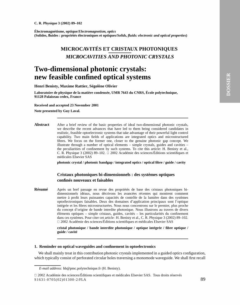
Figure 1. Basic concepts combined in this short review: (a) guided mode in a deep ridge waveguide, obtained byetching; (b) more loosely confined mode in a channel waveguide formed by a shallow ‘dielectric load’ obtained by
lithography from an ordinary dielectric slab waveguide with subsequent etching or deposition; (c) 2D photonic crystalof the ‘dielectric pillar’ type, exhibiting preferentially a TM polarised gap (vertical electric field); (d) 2D photonic
crystal of the hole-array-in-a-matrix type, having preferentially a TE polarised gap (vertical magnetic field).
briefly the various regimes of guiding in integrated optics in order to better place in context the peculiaritiesof photonic crystals.
Confinement in the field of optics is currently achieved in waveguiding systems, which are ubiquitous in,e.g., semiconductor heterostructures, glass fibres, etc. [1]. Planar slabs with a high-index layer sandwichedbetween lower index cladding layers have well-known guiding properties, with two well-defined TE andTM polarisations, allowing one to use a scalar field to describe these properties. To guide light along curvedlines, if not using fibres, one may add an in-plane structuration to the above planar system that will confinelight in one extra dimension. These structure typically come into two ‘flavours’ (Figs. 1a and 1b):(i) deep-etched ridge waveguides, where the lateral cladding is essentially air, and is thus very ‘strong’,
and(ii) shallow-etched systems, or dielectric loaded guides, in which the thickness of the top cladding is locally
larger, pinning an extra mode, with, however, a weaker barrier with respect to sideways optical leakage,as can be measured by the difference in propagation constant β of a mode of the slab and a mode ofthe etched guide, or, more commonly for practitioners in the field, the difference in effective index,neff = βc/ω (with the usual meaning of c and ω).
These channel guides require a full vector treatment in principle, but for many limit cases, one issufficiently close to one of the parent slab guide polarisations to use it as a satisfactory basis. In bothkinds of guiding, however, confinement has some limits. When it comes to bending channel guides, forexample, solution (ii) is particularly poor and imposes a large radius of curvature, 1 cm in silica-basedchannel guides. The situation is better for solution (i) but still far from perfect: a sharp bend will lead to,e.g., mode coupling between quasi-TE and quasi-TM modes.
If one wants further confinement, for example, to define a lasing cavity, or a frequency-selective element,no compact solution is known to implement a mirror at a given position on a channel guide. The ubiquitousDBR solution (distributed Bragg reflector) [1–3] makes use of a shallow grating implemented usually byetching a sinusoidal grating in the cladding layer, leading to a very weak index perturbation; one thousandgrating grooves are then needed to reach acceptable reflection, and only in the restricted spectral stopband of the DBR, less than 1% in relative extent �λ/λ. These are some of the unsatisfactory facts inoptoelectronics. Most attempts to etch stronger and more efficient gratings were plagued by very largeradiation losses out of the guide that occur unless one obeys some geometric requirements on modulationdepth that we will emphasise below and which are, in essence, those of two-dimensional photonic crystalsetched through waveguides. Note however that even compact mirrors based on one-dimensional periodicitycannot provide omnidirectional confinement. In one-dimensional systems, the phase conditions whichensure a gap around a given angle of incidence cannot be maintained for all angles. There will unavoidablybe a range of angles at which radiative modes exist through the periodic structure, so that it is impossibleto build a perfect tiny ‘photon box’ based on such mirrors. The localised modes of such a box are broad ink-space and are thus liable to leak through the radiative modes.
90
To cite this article: H. Benisty et al., C. R. Physique 3 (2002) 89–102
One motivation towards the use of PCs and related localised photon structures is thus compact integrationand diminished sizes, so that the 1000 × 1000 fibres optical switchboard of optical telecommunicationsystems remains small enough. This size reduction is also required in order to enable integration of moredemanding functions such as wavelength transpositions at the nodes of a wavelength-multiplexed (WDM)network. Moreover, photonic crystals made of dielectrics can be very low-loss systems in the optical regime.Thus, they could replace metals in some cases as ‘optical insulators’.
2. Basic properties of ideal two-dimensional photonic crystals
Following the three-dimensional PC concept proposed by Yablonovitch in 1987 [4], it was realisedin the following years that periodic two-dimensional dielectric structures (with invariance along a thirddirection z) can also exhibit a photonic band gap [5,6], i.e., a range of frequency for which in-planepropagation is forbidden because there is no allowed propagative photon state, only evanescent ones. Photonstates in periodic structures are described by a wavevector k running in the Brillouin zone. As for the namingof polarisation, one uses E and H in pure 2D structures to denote those modes with the corresponding fieldalong the invariant direction, the two components of the other field being in the periodicity plane. However,for the sake of consistency with guided optics approaches, we denote E as TM and H as TE.
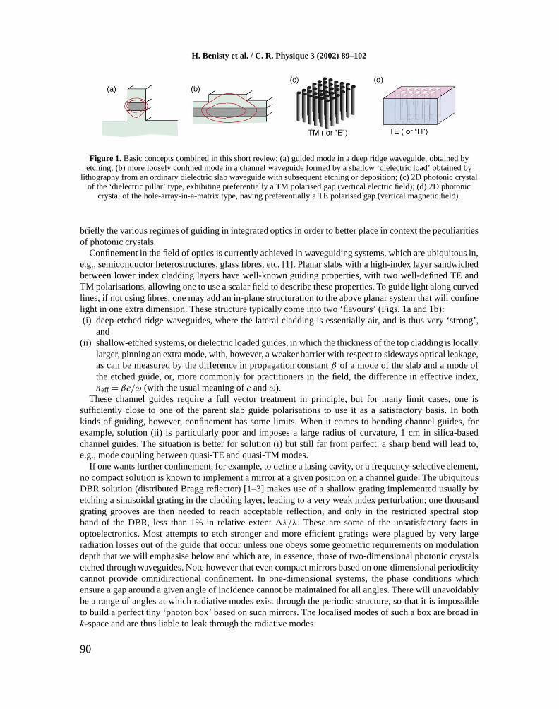
Two kinds of dielectric structures easily provide a band gap at the first gap , as shown in Figs. 1c and 1d(the first gap is the one associated with about the half-wavelength periodicity, taking into account thematerial’s indices, however): the array of pillars provides a TM gap (Fig. 1c), while the array of holes(Fig. 1d ) provide a TE gap. Then, since the central frequency of a gap at the edge of the Brillouin zonescales like the modulus of k, the preferred zone shape is as round as possible, which points to a hexagonalshape and thus a triangular lattice (of period denoted a). We concentrate here on the case of circular airholes (air rods) in a dielectric matrix, which has the advantage of much better compatibility with a dielectricwaveguide implementation in the third direction. Let us introduce the air-filling factor f , which describesthe areal amount of air in the 2D cross section of the PC.
An example of band structure ω(k) with a TE gap and no TM gap is given in Fig. 2a, for a systemwith dielectric constant εm = 11.3 for the matrix and air-filling factor f = 30%. The gap map of Fig. 2brepresents the evolution of both TE and TM gaps in normalised frequency units of u= a/λ= ωa/2πc asa function of f . The Brillouin zone is sketched in Fig. 2c.
Figure 2. 2D photonic crystalconsisting of a triangular
lattice of cylindrical holes:(a) band structure ω(k) for a30% air-filling factor. Notethe overlap of the gap in thevarious directions; (b) ‘gapmap’ describing the full gapevolution as a function of theair-filling factor f . Note the
appearance of the TM gap onthe right. Insets are typicallow- and high-f lattices;
(c) first Brillouin zone withthe �,M and K points.
91
H. Benisty et al. / C. R. Physique 3 (2002) 89–102
While the TE gap in a high-index material is obtained for rather low f values, f = 10–15%, it turns outthat a gap for both polarisations can be obtained at large f values, typically above f = 65%, when veinsbetween holes are thin and the shape left between three holes tends to be pillar-like. However, in the puretwo-dimensional problem, hexagonal lattices of pillars may have quite similar properties to lattice of holes.
Semiconductors possess high enough refractive indices to fulfil the criterion of allowing a band gapcommon to both polarisation (n > 2.6), the criterion for a single polarisation being much less severe (n∼ 2is enough in TE).
What are the basic reflection/transmission properties expected from an ideal two-dimensional PC [7,8]?Many cases are to be distinguished. For a beam impinging normal to the rod axis on a PC of, say, ten unitcells, one expects very weak transmission in the gap, of the order of 10−3 to 10−6. Light not transmitted canbe reflected, but also backward diffracted. In the case of air holes, the impinging medium has a high index(unperforated dielectric), and diffraction of the periodic surface of the PC is likely to occur in the first gap,typically with ±1 diffracted orders allowed. A PC in the gap is thus both a grating and a mirror. Outside thegap, transmission is not granted [8,9]: it depends on the availability of a PC mode to fit the symmetry of theincoming wave, to ensure nonzero coupling. Hence, some ‘transmission gaps’ may occur while photonicstates are present, these states being eventually able to carry away spontaneous emission from an atomsituated inside the PC. Furthermore, when coupling is allowed, spectral transmission properties outside thegap are about those of ‘thick gratings’ [10], with spectral oscillations that depend on the phase taken by theexcited Bloch wave upon achieving round trips in the PC sample. Below the first gap, at large wavelengths,a 2D PC behaves like a sub-wavelength structured material and displays a strong birefringence directlyassociated with the hole direction. The PC sample then behaves as a phase plate.
Finally, what happens at oblique incidence (with a k component along the invariance axis) [11]? Thegap progressively shifts to higher frequency (basically, the same k component in the plane of periodicityis required) and vanishes for a few tens of degrees. The limit case of propagation along the invariancedirection will be discussed specifically in relation with microstructured optical fibres. Let us only underlinehere that only the weaker transverse k components of the field (the ‘beam shape’) are then affected by theperiodicity, and rather little remains from the original interference phenomenon, so that the concept of gap,and the conditions on index and periodicity are to be completely revised.
The only system to date in which structures close to ideal 2D PC have been fabricated in the nearinfrared is macroporous silicon, due to the extraordinary aspect ratio and shape perfection that is obtainedby carefully implementing a photoelectrochemical etching method. Full 2D gaps in the 1.55 µm region,hence with a period of about 600 nm, have been beautifully demonstrated recently [12–17].
3. Defect states
One can classify defects in 2D PC according to their dimensionality: ‘0D’ defects are formed by missingrods or just one or a few modified holes. Such defects introduce modes with eigenfrequencies in the gap.Even a single missing hole supports several such modes within the gap. The photon-in-a-box mode-countingtells us that the number of states in the gap scales like the defect area S. For, e.g., the f = 30% crystaldescribed above, one finds about 0.3 state per missing hole and per 10% bandwidth (about the gap relativewidth).
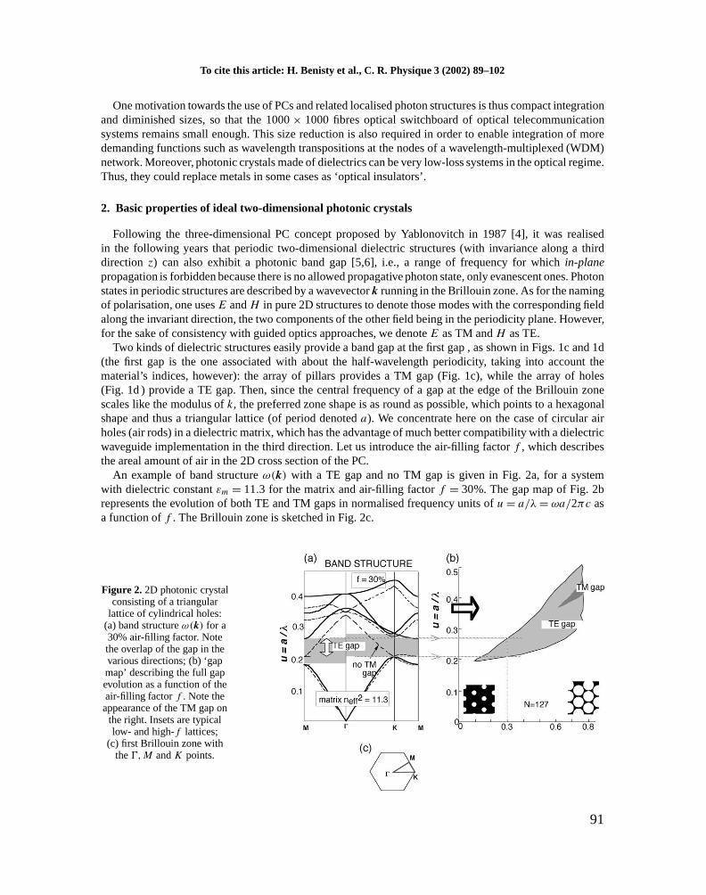
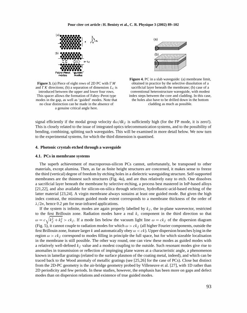
Another canonical class of defects are line defects formed along dense rows according to the schemes ofFig. 3, a–b, whereby a spacer of thickness Lc is introduced. The two halves are PC-based mirrors so that,at normal incidence, it is basically a Fabry–Perot (FP) cavity [18,19] at k// = 0; owing to the periodicity,the modes may be classified using k// [20]. For infinitely thick mirrors, there is no fundamental distinctionbetween the k// = 0 FP modes and modes with k// as high as allowed, in the sense that energy remainsconfined in the cavity for any frequency in the gap. For mirrors of finite PC thickness, say a few rows,the modes unavoidably experience a finite coupling to outside radiations, allowing, e.g., unit transmissionat resonance for a symmetric configuration. This system is also a waveguide that will convey energy or
92
Pour citer cet article : H. Benisty et al., C. R. Physique 3 (2002) 89–102
Figure 3. (a) Piece of eight rows of 2D PC with �Mand �K directions; (b) a separation of dimension Lc is
introduced between the upper and lower four rows.This spacer allows the formation of Fabry–Perot type
modes in the gap, as well as ‘guided’ modes. Note thatno clear distinction can be made in the absence of
a genuine critical angle here.
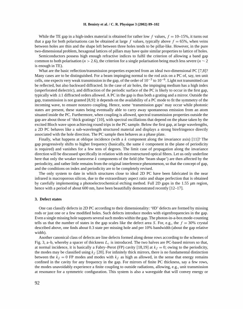
Figure 4. PC in a slab waveguide: (a) membrane limit,obtained in practice by the selective dissolution of asacrificial layer beneath the membrane; (b) case of aconventional heterostructure waveguide, with modest
index steps between the core and cladding. In this case,the holes also have to be drilled down in the bottom
cladding as much as possible.
signal efficiently if the modal group velocity dω/dk// is sufficiently high (for the FP mode, it is zero!).This is closely related to the issue of integrated optics telecommunication systems, and to the possibility ofbending, combining, splitting such waveguides. This will be examined in more detail below. We now turnto the experimental systems, for which the third dimension is quantised.
4. Photonic crystals etched through a waveguide
4.1. PCs in membrane systems
The superb achievement of macroporous-silicon PCs cannot, unfortunately, be transposed to othermaterials, except alumina. Then, as far as finite height structures are concerned, it makes sense to freezethe third (vertical) degree of freedom by etching holes in a dielectric waveguiding structure. Self-supportedmembranes are the thinnest such structures (Fig. 4a), and are thus relatively easy to etch. One dissolvesa sacrificial layer beneath the membrane by selective etching, a process best mastered in InP-based alloys[21,22], and also available for silicon-on-silica through selective, hydrofluoric-acid-based etching of thelatter material [23,24]. A virgin membrane always sustains at least one guided mode. But given the highindex contrast, the minimum guided mode extent corresponds to a membrane thickness of the order ofλ/2n, hence 0.2 µm for near-infrared applications.
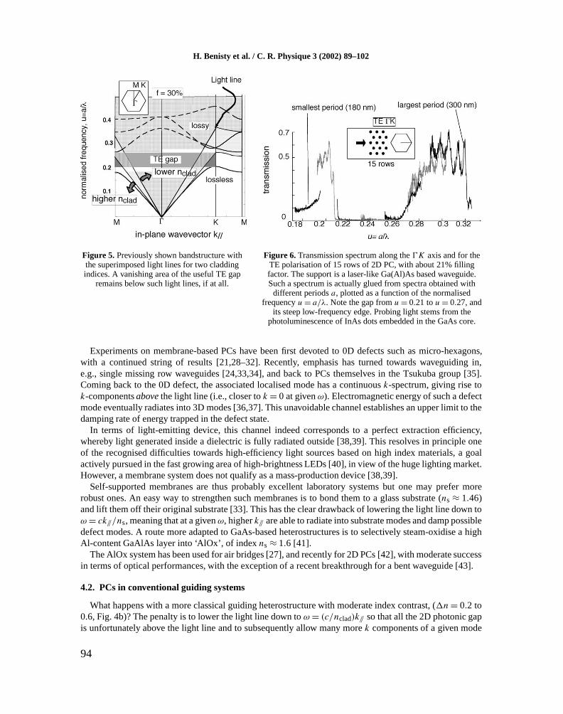
If the system is infinite, modes are again properly labelled by k//, the in-plane wavevector, restrictedto the first Brillouin zone. Radiation modes have a real kz component in the third direction so that
ω = c
√k2// + k2
z > ck//. If a mode lies below the vacuum light line ω = ck// of the dispersion diagram
(Fig. 5), it cannot couple to radiation modes for which ω > ck// (all higher Fourier components, outside thefirst Brillouin zone, feature larger k and automatically obey ω < ck). Upper dispersion branches lying in theregion ω > ck// correspond to modes filling in principle the full space, but for which sizeable localisationin the membrane is still possible. The other way round, one can view these modes as guided modes witha relatively well-defined k// value and a modest coupling to the outside. Such resonant modes give rise toanomalies in transmission or reflection of impinging plane waves at a characteristic angle, a phenomenonknown in lamellar gratings (related to the surface plasmon of the coating metal, indeed), and which can betraced back to the Wood anomaly of metallic gratings (see [25,26] for the case of PCs). Close but distinctfrom the 2D-PC geometry is the air-bridge geometry probed by Villeneuve et al. [27], with 1D rather than2D periodicity and few periods. In these studies, however, the emphasis has been more on gaps and defectmodes than on dispersion relations and existence of true guided modes.
93
H. Benisty et al. / C. R. Physique 3 (2002) 89–102
Figure 5. Previously shown bandstructure withthe superimposed light lines for two claddingindices. A vanishing area of the useful TE gap
remains below such light lines, if at all.
Figure 6. Transmission spectrum along the �K axis and for theTE polarisation of 15 rows of 2D PC, with about 21% fillingfactor. The support is a laser-like Ga(Al)As based waveguide.Such a spectrum is actually glued from spectra obtained with
different periods a, plotted as a function of the normalisedfrequency u= a/λ. Note the gap from u= 0.21 to u= 0.27, and
its steep low-frequency edge. Probing light stems from thephotoluminescence of InAs dots embedded in the GaAs core.
Experiments on membrane-based PCs have been first devoted to 0D defects such as micro-hexagons,with a continued string of results [21,28–32]. Recently, emphasis has turned towards waveguiding in,e.g., single missing row waveguides [24,33,34], and back to PCs themselves in the Tsukuba group [35].Coming back to the 0D defect, the associated localised mode has a continuous k-spectrum, giving rise tok-components above the light line (i.e., closer to k = 0 at given ω). Electromagnetic energy of such a defectmode eventually radiates into 3D modes [36,37]. This unavoidable channel establishes an upper limit to thedamping rate of energy trapped in the defect state.
In terms of light-emitting device, this channel indeed corresponds to a perfect extraction efficiency,whereby light generated inside a dielectric is fully radiated outside [38,39]. This resolves in principle oneof the recognised difficulties towards high-efficiency light sources based on high index materials, a goalactively pursued in the fast growing area of high-brightness LEDs [40], in view of the huge lighting market.However, a membrane system does not qualify as a mass-production device [38,39].
Self-supported membranes are thus probably excellent laboratory systems but one may prefer morerobust ones. An easy way to strengthen such membranes is to bond them to a glass substrate (ns ≈ 1.46)and lift them off their original substrate [33]. This has the clear drawback of lowering the light line down toω = ck///ns, meaning that at a given ω, higher k// are able to radiate into substrate modes and damp possibledefect modes. A route more adapted to GaAs-based heterostructures is to selectively steam-oxidise a highAl-content GaAlAs layer into ‘AlOx’, of index ns ≈ 1.6 [41].
The AlOx system has been used for air bridges [27], and recently for 2D PCs [42], with moderate successin terms of optical performances, with the exception of a recent breakthrough for a bent waveguide [43].
4.2. PCs in conventional guiding systems
What happens with a more classical guiding heterostructure with moderate index contrast, (�n= 0.2 to0.6, Fig. 4b)? The penalty is to lower the light line down to ω = (c/nclad)k// so that all the 2D photonic gapis unfortunately above the light line and to subsequently allow many more k components of a given mode
94
To cite this article: H. Benisty et al., C. R. Physique 3 (2002) 89–102
to radiate away from the guide. We will discuss below conditions for out-of-plane radiation losses to benevertheless acceptable. Following the work by Krauss [44], a collaboration associating our laboratory, theUniversity of Glasgow (C. Smith and T.F. Krauss) and École Polytechnique Fédérale de Lausanne (EPFL,R. Houdré, R. Stanley, U. Oesterle, M. Ilegems) has acquired extensive experience of this kind of 2D PCsfor filling factors f in the range 20–40%, where out-of-plane radiation losses are still affordable.
A quite complete set of transmission, reflection and diffraction measurements of 2D PCs of this kind,etched through a GaAs-based laser-like heterostructure, using photoluminescence of quantum wells orInAs quantum dots as an internal and very practical light source, can be found in the following references[31,45–48]. With QDs, this source is relatively broadband (> 10%), so that combined with ‘lithographictuning’ with ∼ 10% steps of the PC period a, a continuous spectrum is obtained. Typical periods to obtaina gap around 1 µm are a = 200–240 nm, and nominal hole diameters 130 to 160 nm.
Such a combined spectrum using variable periods a (from 180 to 330 nm) is presented in Fig. 6 forN = 15 rows along the �K orientation. The full gap (overlap with the �M gap) extends from u= 0.21 tou= 0.245, over a 15% relative frequency range. Oscillations around the gap are clearly visible. As discussedin [31,46] these oscillations are associated with the interference of Bloch waves undergoing Fabry–Perottype round-trips across the whole crystal (15 rows). Hence, the sizeable amplitude of these oscillationsdemonstrates that a Bloch wave launched at one crystal side suffers modest attenuation upon a round-tripthrough 30 rows of cylinders, about 60 semiconductor/air interfaces. The good accuracy of the pure 2Dpicture to depict this system indicates that the various perturbations (fabrication fluctuations and mostlyradiation losses) are still modest.
The present authors also belong to a European IST consortium ‘PCIC’, IST 11239, gathering teams fromWurzburg University, EPFL (Lausanne), Opto+ in Marcoussis (France), KTH in Kista (Sweden), LPNin Marcoussis (France) and FORTH (Heraklion). This consortium has recently achieved PCs with aboutsimilar spectral behaviour in an InP-based heterostructure, using a single QW as a ∼ 1.5 µm internal lightsource, and closely spaced periods to compensate for the insufficient useful spectral width of the source(about 50 nm) [49]. This validates the generality of the concept, and shows that provided adequate etchingis available, PCs exhibit the expected properties.
4.3. The issue of out-of-plane radiation loss
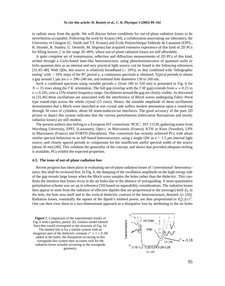
Recent progress has taken place in evaluating out-of-plane radiation losses of ‘conventional’ heterostruc-tures; this shall be reviewed first. In Fig. 6, the damping of the oscillation amplitude on the high energy sideof the gap reveals large losses when the Bloch wave samples the holes rather than the dielectric. This con-firms the intuition that losses occur in the air holes due to the absence of waveguiding. A more quantitativeperturbation scheme was set up in reference [50] based on separability considerations. The radiation lossesthen appear to stem from the radiation of effective dipoles that are proportional to the (average) field Eh inthe hole, the hole area itself and to the vertical dielectric contrast of the heterostructure, denoted �ε [50].Radiation losses, essentially the square of the dipole’s emitted power, are thus proportional to E2
h(�ε)2.
One can then view them in a two-dimensional approach as a dissipative loss by attributing to the air holes
Figure 7. Comparison of the experimental results ofFig. 6 with a perfect, purely 2D, lossless model (dottedline) that would correspond to the structure of Fig. 1d.
The dashed line is for a similar system with animaginary part of the dielectric constant ε∗ = 1 + 0.18i
added in the holes: the dissipation occurring in thiswaveguide-less system then accounts well for the
radiation losses actually occurring in the waveguidegeometry.
95
H. Benisty et al. / C. R. Physique 3 (2002) 89–102
an ad hoc imaginary constant ε′′. Fig. 7 show the success of a fit of the transmission data of Fig. 6 above,made with ε′′ = 0.18 in a simple 2D model [50]. The ability to cast losses of a complex 3D structure into asingle number is indeed quite valuable and may help selecting among various approaches otherwise delicateto compare.
Since then, Lalanne [51] has proposed an exact three-dimensional calculation of the above systems whichhas led to the following refinement: the value of losses pointed out in [50] stems at 80–90% from the finitehole depth z0, a depth which obviously depends on the PC period due to well-known properties of theetching procedure. From this point on, we have established [52] that the excess radiation losses due tofinite hole depth scale essentially like the partial confinement factor �(z0) of the guided wave profile withthe unetched part of the hole. This is the key to quantifying the issue “How deep do I have to etch?”; theother side of this issue is “how much are the intrinsic losses” associated with infinite hole depth. Lalanne’scalculation points to a level of ε′′ ∼ 0.2 for the GaAs system and etching we have used until now, and forwhich the vertical contrast is still relatively large (�ε = 2). Hence, going to low contrast systems such as InP(�ε = 0.5), and achieving sufficient etch depth (�(z0) < 10−3) would probably result in a loss parameterε′′ ∼ 0.005, which would bring these systems very close to ideal ones, with loss-limited reflectivities in the99.5% range, not so far from those of the excellent vertical DBRs used in VCSELs.
As for out-of-plane losses of the membrane system, there is some consensus on the overall picture: inperiodic systems, which include straight guides below, there is some common room between the photonicgap and the light line, so that lossless propagation of modes along a 1D defect is possible. But as soon asperiodicity is broken, as happens for PC-based guide bends and cavities, radiation losses are again there,and it is likely that they are relatively strong: using our perturbation approach, membranes feature a veryhigh �ε of about 10. The situation is thus complex, only that part of the field concerned with the devicesingularity radiates, no modelling tool appears to be able to cast this phenomenon in 2D and loss modellinghas to be made on a time-consuming, per-device basis.
Another delicate issue in both systems is the coupling in and out of PC structures. While our ε′′ ansatzseems to account satisfactorily for such losses in ‘conventional’ substrates, a recent study by Bogaerts etal. [53] suggests that high losses occur at transitions towards membrane type PCs.
5. Controlling light with PCs
5.1. Cavities
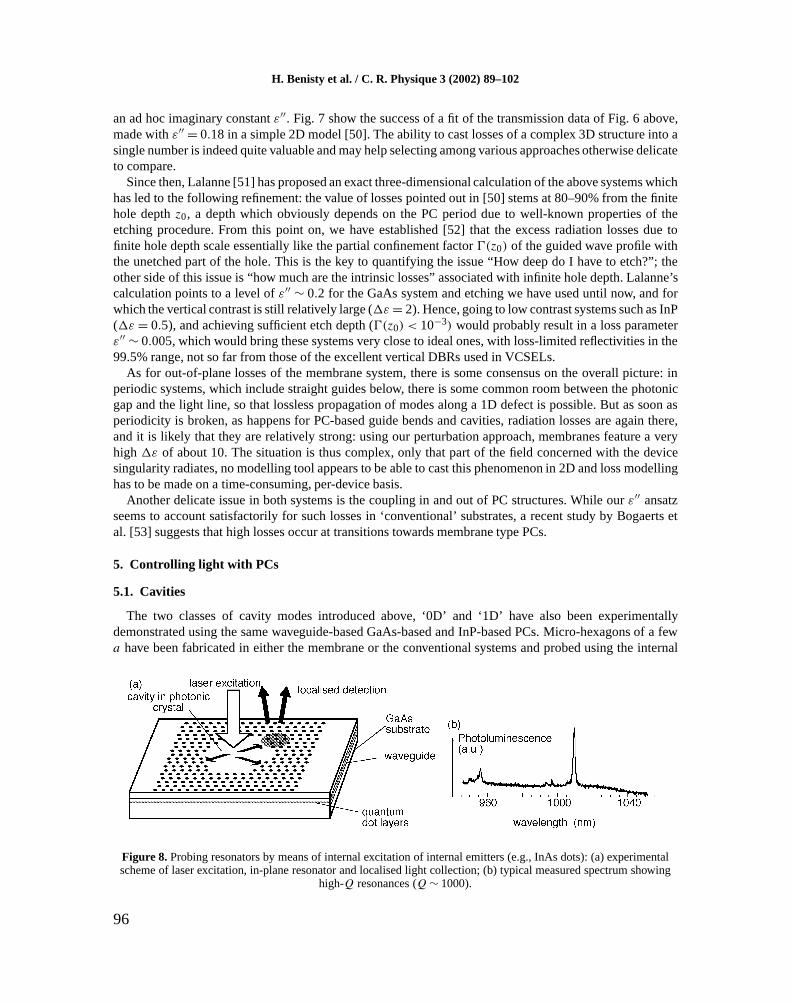
The two classes of cavity modes introduced above, ‘0D’ and ‘1D’ have also been experimentallydemonstrated using the same waveguide-based GaAs-based and InP-based PCs. Micro-hexagons of a fewa have been fabricated in either the membrane or the conventional systems and probed using the internal
Figure 8. Probing resonators by means of internal excitation of internal emitters (e.g., InAs dots): (a) experimentalscheme of laser excitation, in-plane resonator and localised light collection; (b) typical measured spectrum showing
high-Q resonances (Q∼ 1000).
96
Pour citer cet article : H. Benisty et al., C. R. Physique 3 (2002) 89–102
PL of embedded QWs or, better, QDs photoexcited inside the cavity (Fig. 8a) [21,28–32]. Various detectionscheme have been used [29,54]. A typical spectrum for our conventional GaAs-based systems is shownin Fig. 8b for a cavity of side 5a (61 missing holes). Narrow peaks with Q ∼ 1000 clearly appear, whichare the signature of in-plane cavity modes. Note the relative scarcity of these peaks: one expects about 20modes expected for the 10% present relative bandwidth and cavity size. This stems from the poor far-fieldpattern of most of the in-plane modes, which has no reason to give a single lobe towards the collectingoptics, unless the mode is especially symmetrical. These sharp spectral peaks are, anyway, a wonderfulfabrication reproducibility test [30,31].
To obtain, in the simplest way, quantitative information on the quality of confinement, we found that 1Ddefects (Fabry–Perot cavities bounded by PCs) were most interesting [18,19] and in particular, they alloweasy insight into the mirror losses. For PCs of N = 4 rows only, and still the same kind of air-filling factors(20–40%), we introduced a spacer Lc of a few a.
While one expects unit transmission and quality factors of the order of 200–250 in the lossless limit,we found peaks with quality factors Q from 50 to 200 and peak transmissions from 15% to 45% [18,19].Corresponding mirror reflectivities are about R = 90%, with transmission T and losses L each 5% of theremaining 10% power (T +R+L= 1). This shows experimentally that conventional systems can competewell with membranes in terms of reflectivity. Until now, few unambiguous numbers have been publishedon the reflectivity of PCs in membranes [21,55].
5.2. Guides, bends and couplers
Studies on guides and related integrated optics elements (bends, couplers, splitters) started in 1999,with a qualitative contribution [33] and have flourished since then. Along the road of PCs in conventionalsystems, we have demonstrated low-loss guiding (losses less than 50 cm−1), coupling of a cavity and anearby guide [56], and recently, resonant transmission at a bend by means of an inserted cavity [57]. Studieson bends and combiners are also being carried out on InP and GaAs in the framework of PCIC [58,59], withthe successful introduction of end-fire techniques to measure PC guides inserted between ridge guides.
In membrane systems, a number of groups have produced interesting results very recently, among whichare references [43,60] for GaAs on AlOx, [35] for AlGaAs membranes, [24] for SOI, and [61] for a dropfilter on InP. To make a long story short, let us say that, by far, no fully satisfying system has yet appeared,e.g., with broadband bending capability, monomode behaviour and low loss. Presently, no clear estimate ofthe definite merits of all these approaches can be made. In addition to the intrinsic optical figure of meritof any of them, one should also consider how easy it is to cascade elements, what kind of application issought, and in particular whether active devices with PCs are sought [62].
One of the delicate application issues in both cases is to reach an accuracy compatible with theforthcoming wavelength division multiplexing (WDM) standards, either 100 GHz channel spacing with flat40 GHz top, which translate into cavity Q of at least 5000, or 25 GHz spacing for denser systems, with Q
around 20 000. These grids are agreed by the ITU (International Telecommunication Union) and are calledthe ITU grids. Not only are such high Q needed, but also, an array of tens or hundreds of such cavitiesaligned with this ITU grid is required. Presently, the only envisioned solution is post fabrication tuning,either mechanical or electro-optical. The area of mechanical-electrical-micro-systems (MEMS) devoted tooptoelectronics (hence, MOEMS) could provide the desired tuning schemes.
6. Active devices
As PCs were originally devised to control spontaneous emission, it is interesting to include them inlight-emitting devices, namely LEDs and lasers. The ultimate control with an emitter coupled to one ortwo optical defect modes is however extremely difficult in terms of practical applications because of thelarge nonradiative losses induced at etched interfaces, which translates into poor injection yields into theactive quantum states whose optical environment is modified. In GaAs, only some cryogenic model systems
97
H. Benisty et al. / C. R. Physique 3 (2002) 89–102
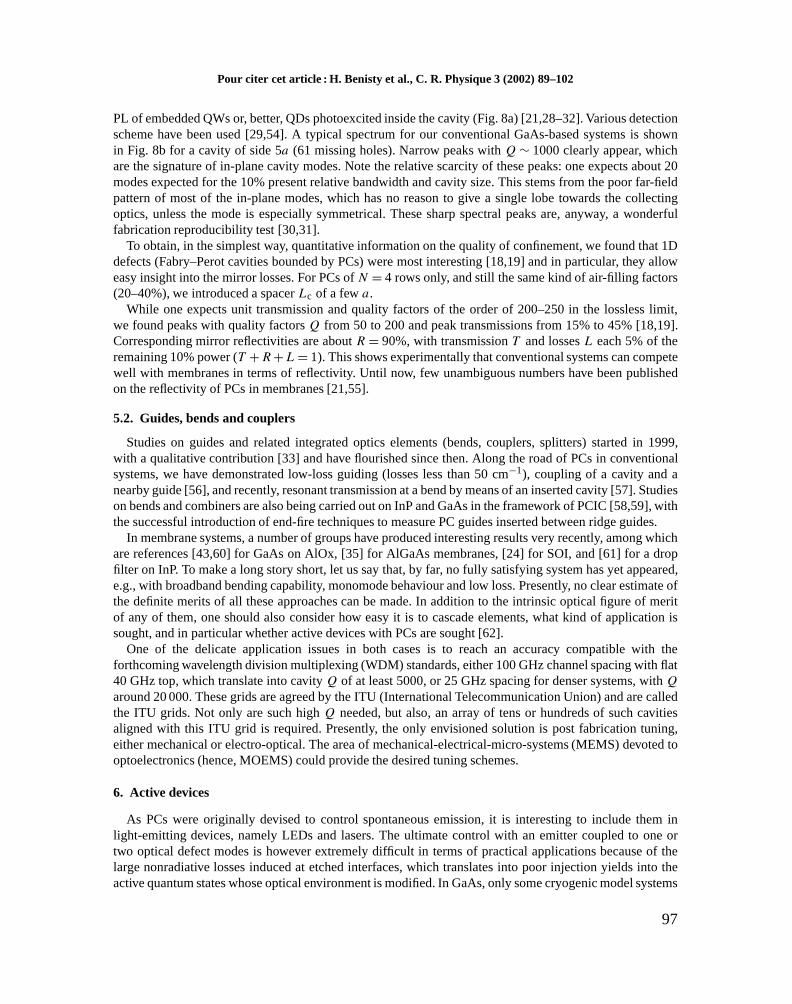
Figure 9. Use of photonic crystal for light extraction in a microcavity-LED: (a) side view, showing the microcavityformed between an air-GaAs interface and a few layers of Bragg mirrors, possibly insulating AlOx-based Braggmirrors. The guided mode carries away a large part of the power from the active layer, which is extracted at the
periphery of the device; (b) top view, showing that the light in the guided mode impinges on the extracting structuresunder a wide range of angles.
(pillars, microdiscs) using quantum dots have shown such interactions. In InP, the much lower nonradiativerecombination penalty has allowed the impressive achievement on a membrane of a room temperatureoptically injected laser based on a single missing hole and a very small (although not ultimate) associatedmode [63,64].
A rather different approach is to seek the modifications of spontaneous emission, and in particular lightextraction, in an infinite 2D PC. Of course, when it is of the slab type, and in-plane propagation is forbidden,very high extraction arises. The more realistic situation of partially etched waveguides has been addressedin some detail by Rigneault [65].
Scanning towards large sizes, we find the above mentioned laser realisation by Raffaele [62], which canreadily be transformed into a 2D PC laser, the use of PCs as laser mirrors [66] or to make ‘bent lasers’ [67],and the work on extraction by Borodistky [39] which is more aimed at enhanced extraction for LEDs. Wehave pursued the use of PCs in somewhat larger LEDs, with the aim of using them as extractors of the guidedmode at the periphery of the active emitting area [41]. The two-dimensional aspect allows light extractionfor a nontrivial set of incidence angles onto the crystal (Fig. 9), a welcome property for extraction. Theoptical properties of these PCs are just the converse of what is expected in integrated optics: no reflection,high radiation losses, in relatively precise directions moreover.
There is however some room to revisit the numerous early day ideas with the concepts of integratedoptics; some such ideas are coupled cavity lasers, power laser diodes and echelle grating integratedspectrometers [68] which were abandoned because of the poor properties (structural and optical) of etchedinterfaces. The advent of novel etching techniques together with the powerful design window opened byPCs is full of promises.
7. Microstructured fibres
Microsructured optical fibres (MOFs), although they belong to a rather different domain of applicationsand tend to address electromagnetism in a somewhat different way given the propagation along the invariantdirection, still retain some of the magic of periodic objects. See [69] and references therein for updated state-of-the-art. Even though the glass/air index contrast is modest, a periodic or even simpler microstructure ina glass fibre may have a huge impact on its modal propagation properties. For a MOF with z axis, guidedmodes have a kz component much larger than the transverse ones kx, ky . A forbidden band of a periodicmicrostructure is then no longer a frequency band with no propagative state at all for in-plane directions,
98
To cite this article: H. Benisty et al., C. R. Physique 3 (2002) 89–102
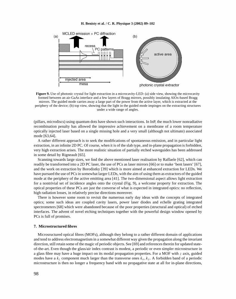
Figure 10.One of the typical layout of silica-basedmicrostructured fibres, consisting of an array of holes, with a
missing hole at the centre that anchors the mode. Anotheralternative is to guide light within an air core using the virtualabsence of light leakage through a properly designed periodic
air/silica structure.
but rather a band with no allowed kx, ky states given some value of kz. If one creates a defect (the core ofthe MOF) in the middle of the periodic structure that can sustain a mode with the adequate kz, it will be abound mode. These MOFs are simple to fabricate from cm-width preforms that are manually stacked with,e.g., some missing ones. Two steps of elongation result in a preserved shape scaled down to the micronscale. Of course, MOFs in a general sense have existed for a long time, e.g., the ‘W’ fibre and polarisationmaintaining ‘panda’ fibres, but the study of periodicity-based MOFs has been prompted by the PC concepts.
Two main kinds of new MOFs are focussing the highest interest:(i) ‘Eternally monomode fibres’ which retain this property over very large spectral ranges, e.g., from
visible to 1550 nm. This is due to the ‘modal sieve’ property of the assembly of the triangular arrayof holes around the core (Fig. 10): any mode that has two lobes in the core is also allowed to extendinto the PC part and loses its guided character. Then, at long wavelength, modes are broad and tend tosee the average PC index, while at short wavelength, they are wavy enough to have nodes at the holesof the PC and see the higher glass index. The complicated transition between these regimes stronglyaffects dispersion. In particular, it allows the zero group velocity delay wavelength to be placed almostanywhere, e.g., around the standard VCSELs wavelengths of 850 nm, meaning that picosecond pulsesmay then travel undistorted for kilometres, avoiding the fate of near infrared pulses in conventionalfibres.
(ii) Fibres supporting a mode essentially in the air, with guidance from the 2D PC Bragg reflection (no totalinternal reflection from air!). This requires quite a lot of air also in the PC cladding. The interestingproperty here is to push away the thresholds for nonlinearities due to the much reduced glass–waveinteraction. Nonlinearities are one of the main limits to fibre capacities. It is hoped that the launchingof waves with powers of watts rather than 10 mW could take place at these fibre entrances without thispenalty. The use of such ‘high power fibres’ in laser-machining with a remote, nonmoving laser is alsoenvisioned.
We will not detail these two types further, but we just note that the losses and imperfections of thesefibres, which limited early experiments in 1996–1998 to centimetric samples, are now much lowered, withpreliminary reports of kilometre long operation for the more robust scheme (i) above (see CLEO 2001post-deadline papers).
8. Conclusions
Optical confinement in more than one dimension has been for a long time a challenge: in optics, basicmicrostructures based on metals tend to be lossy, and are anyway not easy to fabricate; the concept ofphotonic crystal has fed many novel approaches. While it is at its best in theory in 3D, it is clear thatdeterministic structures are much more practical in 2D. Providing the third confinement by means of aconventional waveguide allows recovery of much of what is expected in 3D, e.g., the ability to producehigh-Q photonic boxes. Most of what we have presented is of obvious interest for integrated optics, a fieldin which the planar waveguide is also the basis. PCs in two dimension provide efficient mirrors and cavities(of interest in novel laser devices), they certainly have a high potential to produce by a single lithographic
99
H. Benisty et al. / C. R. Physique 3 (2002) 89–102
step a number of functions such as filtering, guiding, bending, etc., which are beyond the scope of sucha short review, but for which realisations have progressed at an impressive pace during these last two years.For simpler devices such as individual high-brightness LEDs and lasers, these 2D PCs also offer new waysto tackle the electromagnetic issues that are at the heart of the attainment of high, ultimate performancesfor such devices.
Finally, due to their simplicity of use combined with rapid progress in fabrication, microstructured opticalfibres that directly treat existing fibre signals from the point of view of dispersion, nonlinearity, etc., areexpected to be among the first photonic-crystal related products on the market place, in addition to takingan increasing role as a model system in the (engineering) academic realm.
Acknowledgements.The authors acknowledge the support of the European ESPRIT project ‘SMILED’ and of theEuropean IST project ‘PCIC’.
References
[1] T. Tamir (Ed.), Guided Wave Optoelectronics, Springer-Verlag, Berlin, 1990.[2] C. Weisbuch, J. Rarity (Eds.), Microcavities and Photonic Band Gaps: Physics and Applications, Kluwer,
Dordrecht, 1996.[3] H. Benisty, J.-M. Gérard, R. Houdré, J. Rarity, C. Weisbuch (Eds.), Confined Photon Systems: Fundamentals and
Applications, Springer, Heidelberg, 1999.[4] E. Yablonovitch, Inhibited spontaneous emission in solid-state physics and electronics, Phys. Rev. Lett. 58 (1987)
2059–2062.[5] R.D. Meade, K.D. Brommer, A.M. Rappe, J.D. Joannopoulos, Existence of a photonic band gap in two dimensions,
Appl. Phys. Lett. 61 (1992) 495.[6] J.D. Joannopoulos, R.D. Meade, J.N. Winn, Photonic Crystals, Molding the Flow of Light, Princeton University
Press, Princeton, NJ, 1995.[7] M. Sigalas, C.M. Soukoulis, E.N. Economou, C.T. Chan, K.M. Ho, Photonic band gaps and defects in two
dimensions: studies of the transmission coefficient, Phys. Rev. B 48 (1993) 14121–14126.[8] K. Sakoda, Symmetry, degeneracy, and uncoupled modes in two-dimensional photonic lattices, Phys. Rev. B 52
(1995) 7982.[9] W.M. Robertson, G. Arjavalingam, R.D. Meade, K.D. Brommer, A.M. Rappe, J.D. Joannopoulos, Measurement
of photonic band structure in a two-dimensional periodic array, Phys. Rev. Lett. 68 (1992) 2023–2026.[10] H. Kogelnik, C.V. Shank, Coupled wave theory of distributed feedback lasers, J. Appl. Phys. 43 (1972) 2327–2335.[11] X.-P. Feng, Y. Arakawa, Off-plane dependence angle of photonic band gap in a two-dimensional photonic crystal,
IEEE J. Quantum Electron. 32 (1996) 535–541.[12] U. Grüning, V. Lehmann, S. Ottow, K. Busch, Macroporous silicon with a complete 2D PBG centered at 5 µm,
Appl. Phys. Lett. 68 (1996) 747–749.[13] S. Rowson, A. Chelnokov, J.-M. Lourtioz, Macroporous silicon photonic crystals at 1.55 micrometers, Electron.
Lett. 35 (1999) 753–755.[14] A. Birner, U. Gruning, S. Ottow, A. Schneider, F. Müller, V. Lehmann, H. Föll, U. Gösele, Macroporous silicon: a
two-dimensional photonic bandgap material suitable for the near-infrared spectral range, Phys. Status Solidi A 165(1998) 111–117.
[15] S. Rowson, A. Chelnokov, J.M. Lourtioz, F. Carcenac, Reflection and transmission characterisation of a hexagonalphotonic crystal in the mid infrared, J. Appl. Phys. 83 (1998) 5061.
[16] S.W. Leonard, H.M. van Driel, A. Birner, U. Gösele, P.R. Villeneuve, Single-mode transmission in two-dimensional maroporous silicon photonic crystal waveguides, Opt. Lett. 25 (2000) 1550–1552.
[17] S.W. Leonard, H.M. van Driel, K. Busch, S. John, A. Birner, A.-P. Li, F. Müller, U. Gösele, V. Lehmann,Attenuation of optical transmission within the band gap of thin two-dimensional macroporous silicon photoniccrystals, Appl. Phys. Lett. 75 (1999) 3063–3065.
[18] C.J.M. Smith, T.F. Krauss, R.M. De La Rue, D. Labilloy, H. Benisty, C. Weisbuch, U. Oesterle, R. Houdré,In-plane microcavity resonators with two-dimensional photonic bandgap mirrors, IEE-Proc.-Optoelectron. 145(1998) 373–378.
[19] M. Rattier, H. Benisty, C.J.M. Smith, A. Béraud, D. Cassagne, T.F. Krauss, C. Weisbuch, Performanceof waveguide-based two-dimensional photonic-crystal mirrors studied with Fabry–Pérot resonators, IEEEJ. Quantum Electron. 37 (2001) 237–243.
[20] H. Benisty, Modal analysis of optical guides with two-dimensional photonic band-gap boundaries, J. Appl.Phys. 79 (1996) 7483–7492.
100
Pour citer cet article : H. Benisty et al., C. R. Physique 3 (2002) 89–102
[21] P. Pottier, C. Seassal, X. Letartre, J.L. Leclercq, P. Viktorovitch, D. Cassagne, C. Jouanin, Triangular andhexagonal high Q-Factor 2D photonic bandgap cavities on III–V suspended membranes, J. Lightwave Technol. 17(1999) 2058–2062.
[22] N.L. Dantec, T. Benyattou, G. Guillot, A. Spisser, C. Seassal, J.L. Leclercq, P. Viktorovitch, D. Rondi,R. Blondeau, Tunable microcavity based on InP-Air Bragg mirrors, IEEE J. Quantum Electron. 5 (1999) 111–114.
[23] M. Loncar, T. Doll, J. Vuckovic, A. Sherrer, Design and fabrication of silicon photonic crystal optical waveguides,J. Lightwave Technol. 18 (2000) 1402–1411.
[24] M. Loncar, D. Nedeljkovic, T. Doll, J. Vuckovic, A. Sherrer, T. Pearsall, Waveguiding in planar photonic crystals,Appl. Phys. Lett. 77 (2000) 1937–1939.
[25] V.N. Astratov, I.N. Culshaw, R.M. Stevenson, D.M. Whittaker, M.S. Skolnick, T.F. Krauss, R.M.D.L. Rue,Resonant coupling of near-infrared radiation to photonic band structure waveguides, J. Lightwave Technol. 17(1999) 2050–2057.
[26] D.M. Whittaker, I.S. Culshaw, Scattering-matrix treatment of patterned multilayer photonic structures, Phys. Rev.B 60 (1999) 2610–2618.
[27] P.R. Villeneuve, S. Fan, J.D. Joannopoulos, K.Y. Lim, G.S. Petrich, L.A. Kolodzlejski, R. Reif, Air bridgemicrocavities, Appl. Phys. Lett. 67 (1995) 167–169.
[28] R.K. Lee, O.J. Painter, B. D’Urso, A. Scherer, A. Yariv, Measurement of spontaneous emission from a two-dimensional photonic band gap defined microcavity at near-infrared wavelengths, Appl. Phys. Lett. 71 (1999)1522–1524.
[29] C.J.M. Smith, T.F. Krauss, R.M. De La Rue, D. Labilloy, H. Benisty, C. Weisbuch, U. Oesterle, R. Houdré, Near-infrared microcavities confined by two-dimensional photonic bandgap crystals, Electron. Lett. 35 (1999) 228–230.
[30] C.J.M. Smith, T.F. Krauss, H. Benisty, M. Rattier, C. Weisbuch, U. Oesterle, R. Houdré, Directionnally dependentconfinement in photonic-crystal microcavities, J. Opt. Soc. Am. B 17 (2000) 2043–2051.
[31] H. Benisty et al., Optical and confinement properties of two-dimensional photonic crystals, J. LightwaveTechnol. 17 (1999) 2063–2077.
[32] C. Reese, C. Becher, A. Imamoglu, E. Hu, B.D. Gerardot, P.M. Petroff, Photonic crystal microcavities with self-assembled InAs quantum dots as active emitters, Appl. Phys. Lett. 78 (2001) 2279–2281.
[33] T. Baba, N. Fukaya, J. Yonekura, Observation of light propagation in photonic crystal optical waveguides withbends, Electron. Lett. 35 (1999) 654–655.
[34] M. Tokushima, H. Kosaka, A. Tomita, H. Yamada, Lightwave propagation through a 120◦ sharply bent single-line-defect photonic crystal waveguide, Appl. Phys. Lett. 76 (2000) 952–954.
[35] N. Kawai, K. Inoue, N. Carlsson, N. Ikeda, Y. Sugimoto, K. Asakawa, T. Takemori, Confined band gap in anair-bridge type of two-dimensional AlGaAs photonic crystal, Phys. Rev. Lett. 86 (2001) 2289–2292.
[36] B. D’Urso, O. Painter, J. O’Brien, T. Tombrello, A. Yariv, A. Scherer, Modal reflectivity in finite-depth two-dimensional photonic crystal microcavities, J. Opt. Soc. Am. B 15 (1998) 1155–1159.
[37] O. Painter, J. Vuckovic, A. Scherer, Defect modes of a two-dimensional crystal in an optically thin dielectric slab,J. Opt. Soc. Am. B 16 (1999) 275–285.
[38] S. Fan, P.R. Villeneuve, J.D. Joannopoulos, High extraction efficiency of spontaneous emission from slabs ofphotonic crystals, Phys. Rev. Lett. 78 (1997) 3294.
[39] M. Boroditsky, T.F. Krauss, R. Coccioli, R. Vrijen, R. Bhat, E. Yablonovitch, Light extraction from opticallypumped light-emitting diode by thin-slab photonic crystal, Appl. Phys. Lett. 75 (1999) 1036–1038.
[40] M.R. Krames et al., High-power truncated-inverted-pyramid (AlxGa1−x)0.5In0.5P/GaP light-emitting diodesexhibiting > 50% external quantum efficiency, Appl. Phys. Lett. 75 (1999) 2367.
[41] M. Rattier et al., High extraction efficiency, laterally injected, light emitting diodes combining microcavities andphotonic crystals, Opt. Quantum Electron., in press.
[42] E. Chow et al., Three-dimensional control of light in a two-dimensional crystal slab, Nature 407 (2000) 983–986.[43] E. Chow, S.Y. Lon, J.R. Wendt, S.G. Johnson, J.D. Joannopoulos, Quantitative analysis of bending efficiency in
photonic crystal waveguide bends at λ= 1.55 µm wavelengths, Opt. Lett. 26 (2001) 286–288.[44] T.F. Krauss, R.M. De La Rue, S. Brand, Two-dimensional photonic-bandgap structures operating at near-infrared
wavelengths, Nature 383 (1996) 699–702.[45] D. Labilloy et al., in: H. Benisty, J.-M. Gérard, R. Houdré, J. Rarity, C. Weisbuch (Eds.), Fundamentals and
Applications of Confined Photon Systems, Springer, Heidelberg, 1999.[46] D. Labilloy, H. Benisty, C. Weisbuch, C.J.M. Smith, T.F. Krauss, R. Houdré, U. Oesterle, Finely resolved
transmission spectra and band structure of two-dimensional photonic crystals using InAs quantum dots emission,Phys Rev. B 59 (1999) 1649–1652.
[47] D. Labilloy et al., Quantitative measurement of transmission, reflection and diffraction of two-dimensionalphotonic bandgap structures at near-infrared wavelengths, Phys. Rev. Lett. 79 (1997) 4147–4150.
101
H. Benisty et al. / C. R. Physique 3 (2002) 89–102
[48] D. Labilloy, H. Benisty, C. Weisbuch, T.F. Krauss, R. Houdré, U. Oesterle, Use of guided spontaneous emission ofa semiconductor to probe the optical properties of two-dimensional photonic crystals, Appl. Phys. Lett. 71 (1997)738–740.
[49] See the Optimist web site of the IST-EU program, http://www.intec.rug.ac.be/ist-optimist/wshp.asp.[50] H. Benisty, D. Labilloy, C. Weisbuch, C.J.M. Smith, T.F. Krauss, A. Béraud, D. Cassagne, C. Jouanin, Radiation
losses of waveguide-based two-dimensional photonic crystals: positive role of the substrate, Appl. Phys. Lett. 76(2000) 532–534.
[51] P. Lalanne, H. Benisty, Ultimate limits of two-dimensional photonic crystals etched through waveguides: anelectromagnetic analysis, J. Appl. Phys. 89 (2001) 1512–1514.
[52] H. Benisty, P. Lalanne, S. Olivier, M. Rattier, C. Weisbuch, C.J.M. Smith, T.F. Krauss, C. Jouanin, D. Cassagne,Finite-depth and intrinsic losses in vertically etched two-dimensional photonic crystals, Opt. Quantum Electron.,in press.
[53] W. Bogaerts et al., Out-of-plane scattering in photonic crystals, IEEE Phot. Technol. Lett. 13 (2001) 565–567.[54] D. Labilloy, H. Benisty, C. Weisbuch, T.F. Krauss, C.J.M. Smith, R. Houdré, U. Oesterle, High-finesse disk
microcavity based on a circular Bragg reflector, Appl. Phys. Lett. 73 (1998) 1314–1316.[55] C. Grillet et al., Characterisation of 2D photonic crystals cavities on InP membranes, Eur. Phys. J. D, in press;
X. Letartre, C. Seassal, C. Grillet, Group velocity and propagation losses measurement in a single-line photonic-crystal waveguide on InP membranes, Appl. Phys. Lett. 79 (2001) 2312.
[56] C.J.M. Smith, R.M. De La Rue, M. Rattier, S. Olivier, H. Benisty, C. Weisbuch, T.F. Krauss, R. Houdré,U. Oesterle, Coupled guide and cavity in a two-dimensional photonic crystal, Appl. Phys. Lett. 78 (2001) 1487–1489.
[57] S. Olivier, H. Benisty, M. Rattier, C. Weisbuch, M. Qiu, A. Karlsson, C.J.M. Smith, R. Houdré, U. Oesterle,Resonant and nonresonant transmission through waveguide bends in a planar photonic crystal, Appl. Phys. Lett. 79(2001) 2514–2516.
[58] A. Talneau, L. Le Gouezigou, N. Bouadma, Quantitative measurements of low propagation losses at 1.55 µm onplanar photonic crystal waveguides, Opt. Lett. 26 (2001) 1259–1261.
[59] J. Moosbürger, M. Kamp, A. Forchel, Paper JTuB2, Transmission spectra measurements on photonic crystalsbased bent waveguides, in: CLEO, Baltimore, May 6–11, 2001.
[60] S.Y. Lin, E. Chow, S.G. Johnson, J.D. Joannopoulos, Demonstration of highly efficient waveguiding in a photoniccrystal slab at the 1.5 µm wavelength, Opt. Lett. 25 (2000) 1297–1299.
[61] S. Noda, A. Chutinan, M. Imada, Trapping and emission of photons by a single defect in a photonic bandgapstructure, Nature 407 (2000) 608–610.
[62] L. Raffaele, R.M. De La Rue, J.S. Roberts, T.F. Krauss, Edge-emitting semiconductor microlasers with ultrashort-cavity and dry-etched high-reflectivity photonic microstructure mirrors, IEEE Photon. Technol. Lett. 13 (2001)176–178.
[63] O.J. Painter, A. Husain, A. Scherer, J.D. O’Brien, I. Kim, Dapkus, Room temperature photonic crystal defectlasers at near-infrared wavelengths in InGaAsP, J. Lightwave Technol. 17 (1999) 2082–2088.
[64] H.-G. Park, J.-K. Hwang, J. Huh, H.-Y. Ryu, Y.-H. Lee, J.-S. Kim, Nondegenerate monopole-mode two-dimensional photonic band gap laser, Appl. Phys. Lett. 79 (2001) 3032–3034.
[65] H. Rigneault, F. Lemarchand, A. Sentenac, Dipole radiation into grating structures, J. Opt. Soc. Am. A 17 (2000)1048–1058.
[66] M. Forchel et al., Lasers with PBG mirrors, in: IPRM’99, Davos, 1999.[67] T.D. Happ, M. Kamp, F. Klopf, J.P. Reithmaier, A. Forchel, Bent laser cavity based on 2D photonic crystal
waveguide, Electron. Lett. 26 (2000) 324–325.[68] R. März, in: B. Culshaw, A. Rogers, A. Taylor (Eds.), Integrated Optics: Design and Modeling, The Artech House
Optoelectronics Library, Artech House, Boston, 1994.[69] A. Ortigosa-Blanch, J.C. Knight, W.J. Wadsworth, J. Arriaga, B.J. Mangan, T.A. Birks, P.St.J. Russel, Highly
birefringent photonic crystal fibres, Opt. Lett. 25 (2000) 1325–1327.
102


![divine [id] - didhbgt€¦ · Web view2018/07/20 · Hamel-Desnos C., Desnos P., Allaert F-A, Kern P. Thermal ablation of saphenous veins is feasible and safe in patients older than](https://img.pdfslide.fr/doc/110x75/5f3e01b9ba1fa24146718712/divine-id-didhbgt-web-view-20180720-hamel-desnos-c-desnos-p-allaert.jpg)


![Reproductive Biology and Endocrinology BioMed Central...high lipid content, and the polar organization [6]. There-fore, the most feasible method for ex situ management of genetic resources](https://img.pdfslide.fr/doc/110x75/614a979612c9616cbc698415/reproductive-biology-and-endocrinology-biomed-central-high-lipid-content-and.jpg)