CRISTECH Brice GAUTIEROctobre 2020
1
Mesure à l'échelle nanométrique des propriétés électriques des matériaux par les techniques dérivées de la microscopie à force atomique
Brice GAUTIER
Institut des Nanotechnologies de LyonINSA de Lyon
David ALBERTINI, Alexander SYNGAEVSKI
CRISTECH Brice GAUTIEROctobre 2020
2
Sommaire
Atomic Force Microscopy modes● Contact● Non contact● Intermittent● Peak Force
Current measurements● Leakage currents in oxides● Dopants concentration in semiconductors
Capacitance measurements● Dopants concentration in semiconductors● Charges in oxides
Piezoelectric measurements● Dielectric polarisation in ferroelectrics and piezoelectrics
Electric field and potential measurements● Surface charges on ferroelectrics
p n

CRISTECH Brice GAUTIEROctobre 2020
3
Near field microscopies
CRISTECH Brice GAUTIEROctobre 2020
4
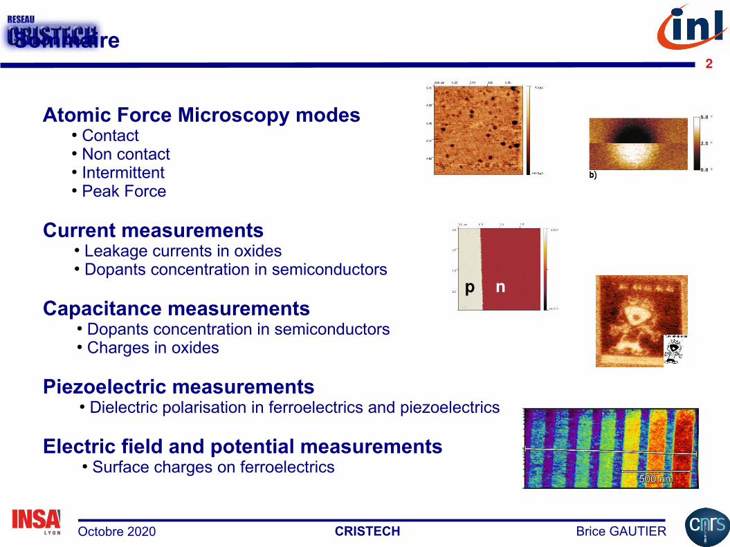
Scanning Tunneling Microscopy (STM) : tunneling current
Principle : measure the current flowing between the (metallic) tip and the (conducting) surface
The electrical circuit is not closed (gap of several nanometers)
=> only tunnel current can flow !
http://www.iap.tuwien.ac.at/www/surface/STM_Gallery/index.htmlxI varies exponentially
=> allows a precise adjustment of the distance
K : constant value : depends on the nature of the surface
dV
I ∼ V e−2Kd
1981 : Scanning Tunneling Microscope
CRISTECH Brice GAUTIEROctobre 2020
5
V
iThinned tungsten wire
Conducting surface
Feed-backV
piezo
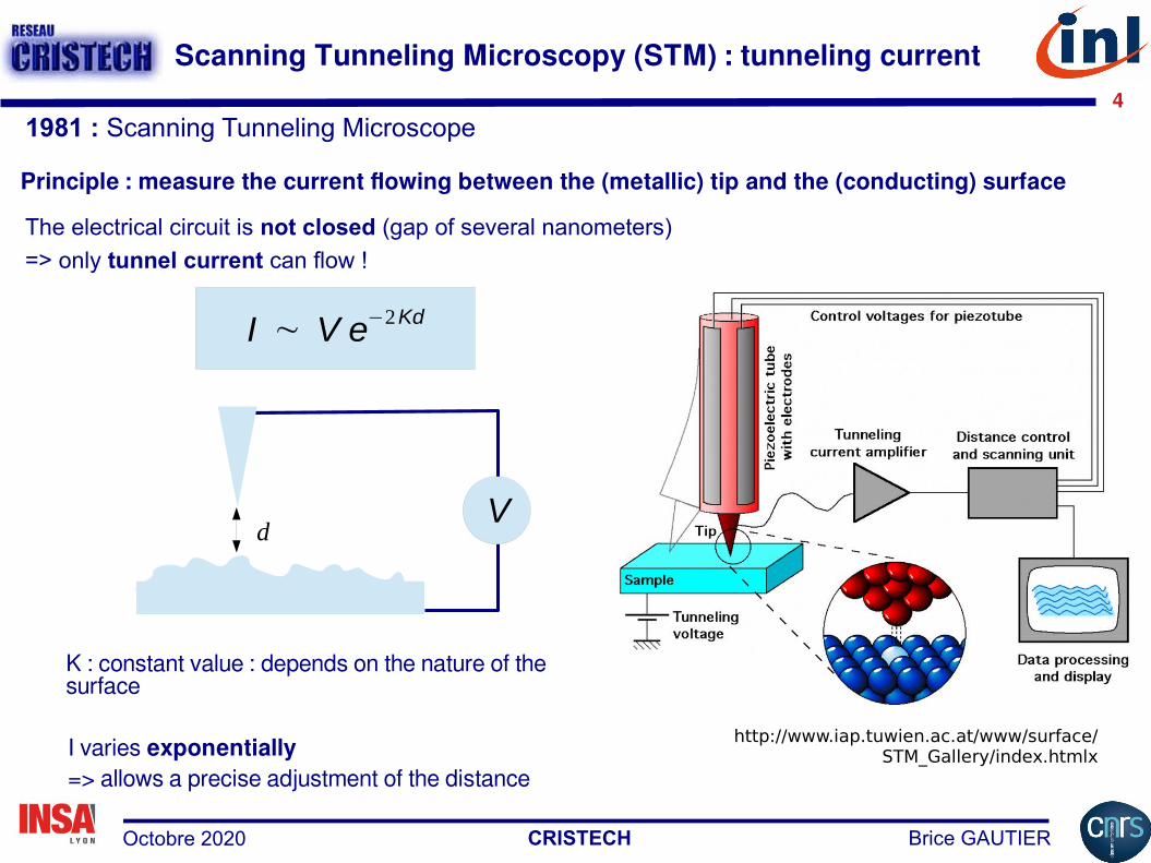
Current I is kept constant at each point
Distance d is adjustedVoltage V applied on piezotube is used to adjust d
The STM signal is a voltage representing the local electronic density of states
STM has to be preferably implemented in Ultra-High Vacuum (pressure < 10-10 mbar) and with conducting samples
Scanning Tunneling Microscopy : principle
I ∼ V e−2Kd
V(x,y) represents the height map
(111) Silicon boron doped
F. Palmino et al., univ. Franche Comté
7X7 Silicon surface imaged by STM under UHV
CRISTECH Brice GAUTIEROctobre 2020
6
What happens with non conductive samples ?
Atomic force microscopy
CRISTECH Brice GAUTIEROctobre 2020
7
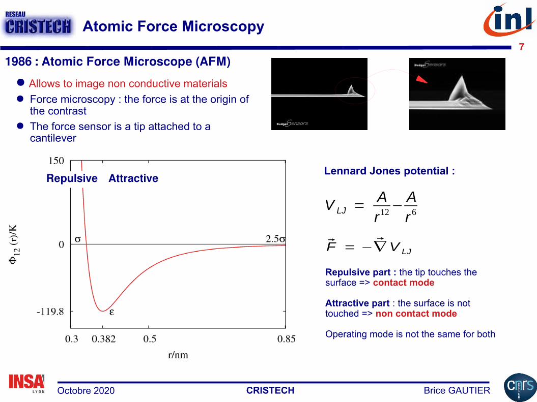
● Allows to image non conductive materials● Force microscopy : the force is at the origin of
the contrast● The force sensor is a tip attached to a
cantilever
Repulsive part : the tip touches the surface => contact mode
Attractive part : the surface is not touched => non contact mode
Operating mode is not the same for both
V LJ = Ar12
−Ar 6
F⃗ = −∇⃗ V LJ
AttractiveRepulsiveLennard Jones potential :
Atomic Force Microscopy
1986 : Atomic Force Microscope (AFM)
CRISTECH Brice GAUTIEROctobre 2020
8
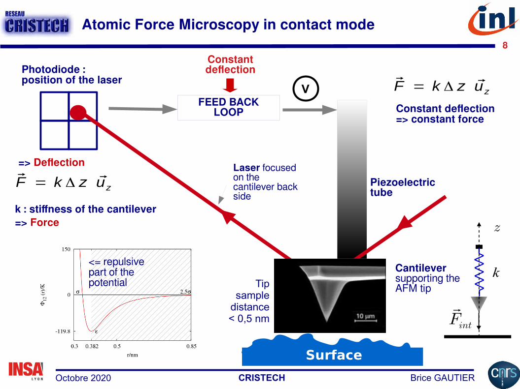
Atomic Force Microscopy in contact mode
Piezoelectric tube
Laser focused on the cantilever back side
Surface
V
Cantilever supporting the AFM tip
FEED BACK LOOP
Constant deflection
Constant deflection=> constant force
F⃗ = k Δ z u⃗z
Photodiode : position of the laser
F⃗ = k Δ z u⃗z
=> Deflection
k : stiffness of the cantilever => Force
Tip sample
distance < 0,5 nm
<= repulsive part of the potential
CRISTECH Brice GAUTIEROctobre 2020
9
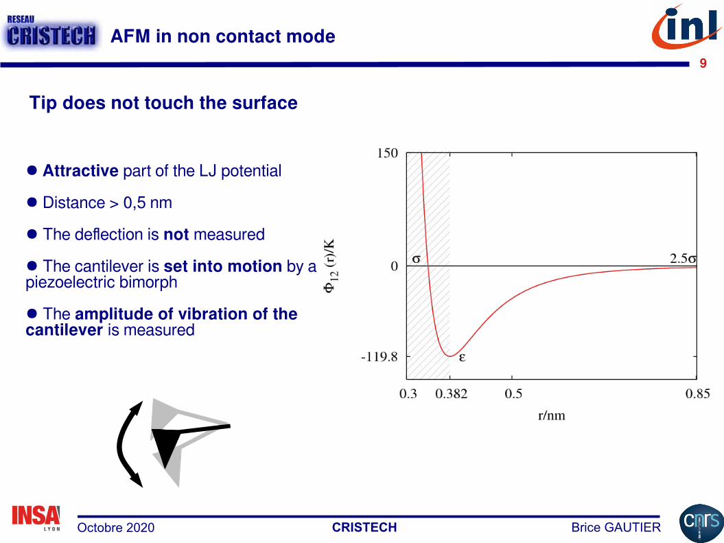
AFM in non contact mode
Tip does not touch the surface
● Attractive part of the LJ potential
● Distance > 0,5 nm
● The deflection is not measured
● The cantilever is set into motion by a piezoelectric bimorph
● The amplitude of vibration of the cantilever is measured
CRISTECH Brice GAUTIEROctobre 2020
10
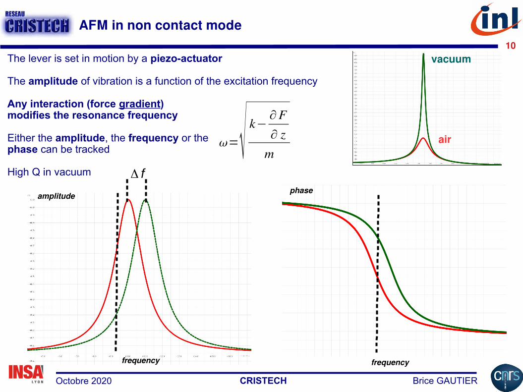
AFM in non contact mode
ω=√ k−∂F∂ zm
frequency
amplitudephase
frequency
vacuum
air
Δ f
The lever is set in motion by a piezo-actuator
The amplitude of vibration is a function of the excitation frequency
Any interaction (force gradient) modifies the resonance frequency
Either the amplitude, the frequency or the phase can be tracked
High Q in vacuum
CRISTECH Brice GAUTIEROctobre 2020
11
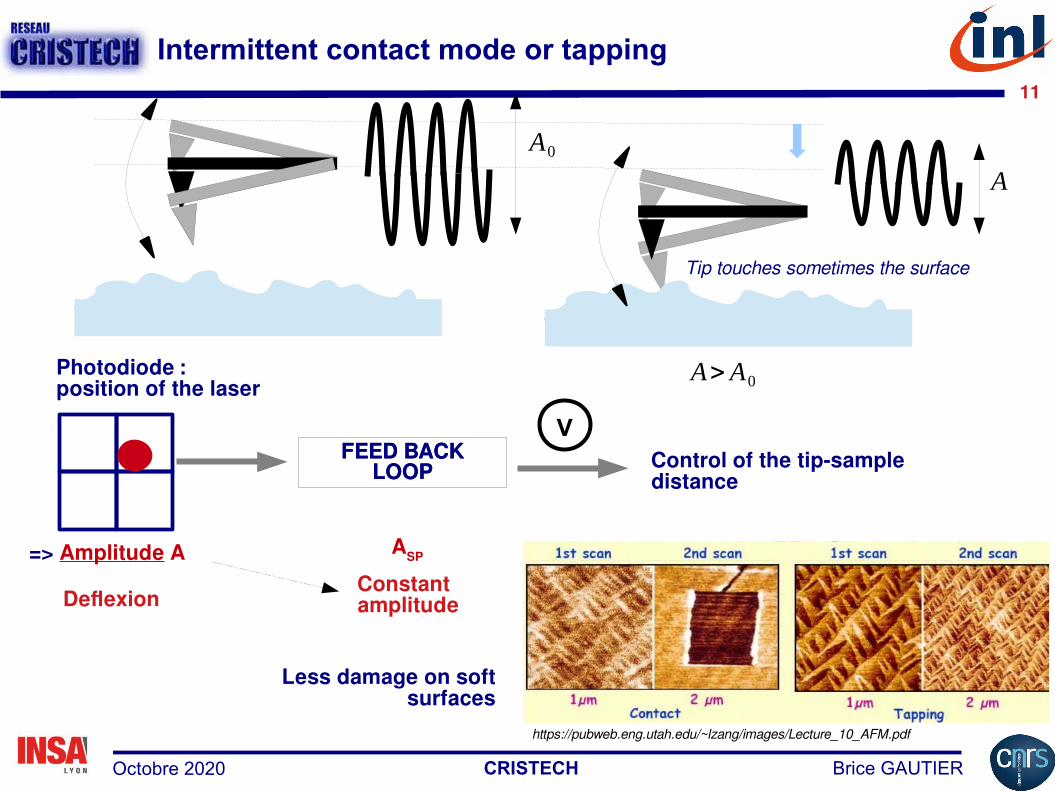
Intermittent contact mode or tapping
A0
A
A>A0
FEED BACK LOOP
Photodiode : position of the laser
=> Amplitude A
VControl of the tip-sample distance
ASP
Constant amplitude
Less damage on soft surfaces
https://pubweb.eng.utah.edu/~lzang/images/Lecture_10_AFM.pdf
Tip touches sometimes the surface
FEED BACK LOOP
Deflexion
CRISTECH Brice GAUTIEROctobre 2020
12
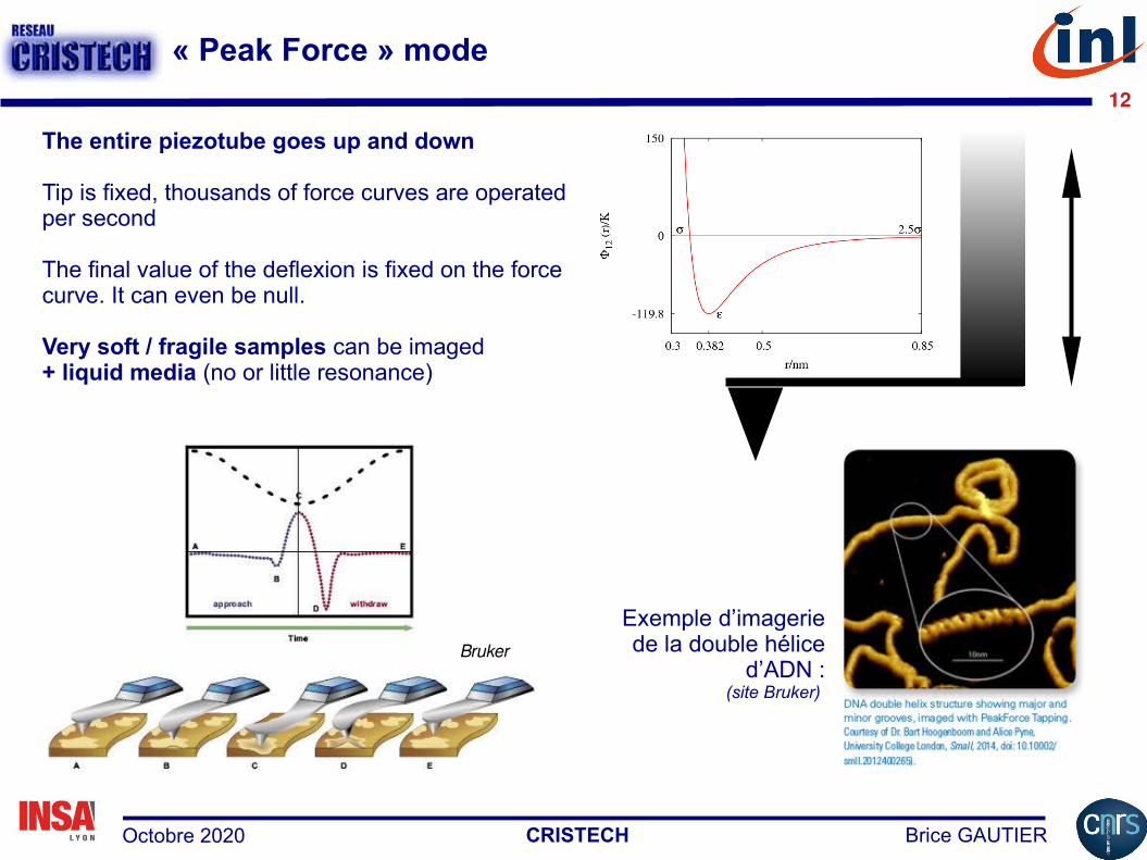
« Peak Force » mode
The entire piezotube goes up and down
Tip is fixed, thousands of force curves are operated per second
The final value of the deflexion is fixed on the force curve. It can even be null.
Very soft / fragile samples can be imaged+ liquid media (no or little resonance)
Exemple d’imagerie de la double hélice
d’ADN : (site Bruker)
Bruker

CRISTECH Brice GAUTIEROctobre 2020
13
Electrical measurements with an AFM
CRISTECH Brice GAUTIEROctobre 2020
14
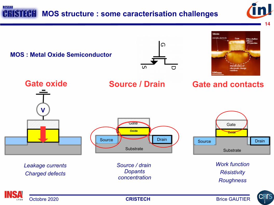
MOS structure : some caracterisation challenges
V
MOS : Metal Oxide Semiconductor
Leakage currents
Charged defects
Source Drain
Oxide
Substrate
Gate
Source / drain Dopants
concentration
Source Drain
Oxide
Substrate
Gate
Work function
Résistivity
Roughness
Gate and contactsSource / DrainGate oxide
CRISTECH Brice GAUTIEROctobre 2020
15
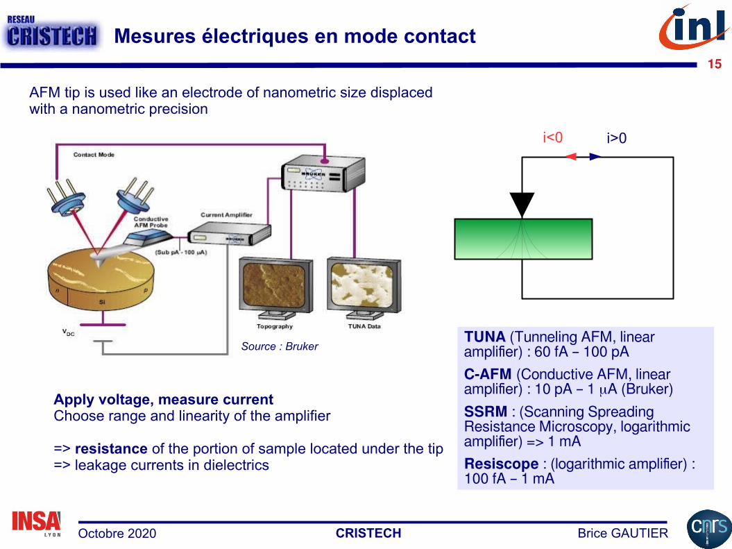
Mesures électriques en mode contact
AFM tip is used like an electrode of nanometric size displaced with a nanometric precision
Source : Bruker
Apply voltage, measure currentChoose range and linearity of the amplifier
=> resistance of the portion of sample located under the tip=> leakage currents in dielectrics
i>0i<0
TUNA (Tunneling AFM, linear amplifier) : 60 fA – 100 pA
C-AFM (Conductive AFM, linear amplifier) : 10 pA – 1 mA (Bruker)
SSRM : (Scanning Spreading Resistance Microscopy, logarithmic amplifier) => 1 mA
Resiscope : (logarithmic amplifier) : 100 fA – 1 mA
CRISTECH Brice GAUTIEROctobre 2020
16
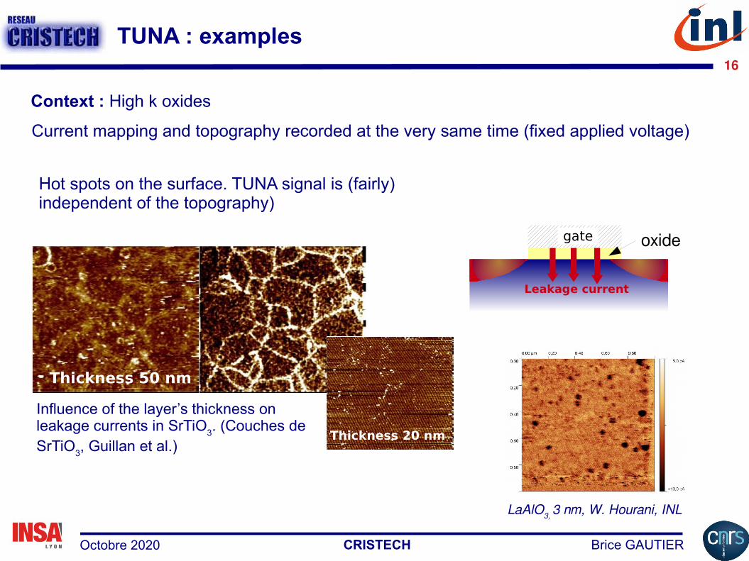
TUNA : examples
épaisseur 50 nm
Current mapping and topography recorded at the very same time (fixed applied voltage)
Hot spots on the surface. TUNA signal is (fairly) independent of the topography)
Context : High k oxides
Thickness 20 nm
Thickness 50 nm
Influence of the layer’s thickness on leakage currents in SrTiO
3. (Couches de
SrTiO3, Guillan et al.)
Leakage current
gate oxide
LaAlO3, 3 nm, W. Hourani, INL
CRISTECH Brice GAUTIEROctobre 2020
17
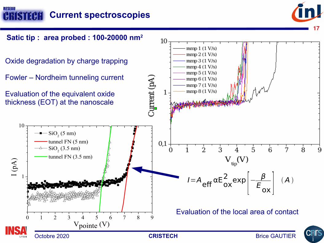
Current spectroscopies
Oxide degradation by charge trapping
Fowler – Nordheim tunneling current
Evaluation of the equivalent oxide thickness (EOT) at the nanoscale
Satic tip : area probed : 100-20000 nm2
I=Aeff
αEEox2 exp [−
βE
ox ] A
0 1 2 3 4 5 6 7 8 9
1
10
I (p
A)
Vpointe (V)
SiO2 (5 nm)
tunnel FN (5 nm) SiO
2 (3.5 nm)
tunnel FN (3.5 nm)
Evaluation of the local area of contact
CRISTECH Brice GAUTIEROctobre 2020
18
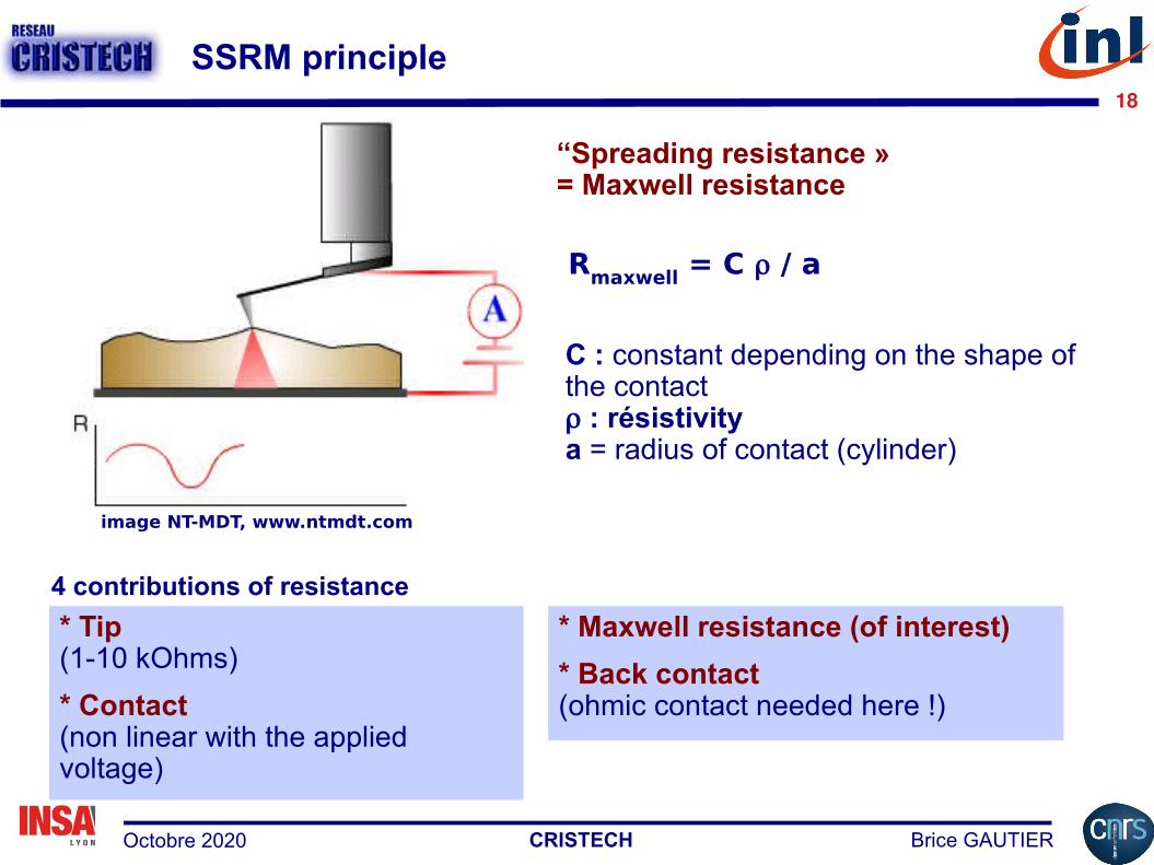
SSRM principle
“Spreading resistance »= Maxwell resistance
Rmaxwell = C r / a
C : constant depending on the shape of the contactr : résistivitya = radius of contact (cylinder)
image NT-MDT, www.ntmdt.com
* Tip(1-10 kOhms)
* Contact(non linear with the applied voltage)
4 contributions of resistance
* Maxwell resistance (of interest)
* Back contact(ohmic contact needed here !)
CRISTECH Brice GAUTIEROctobre 2020
19
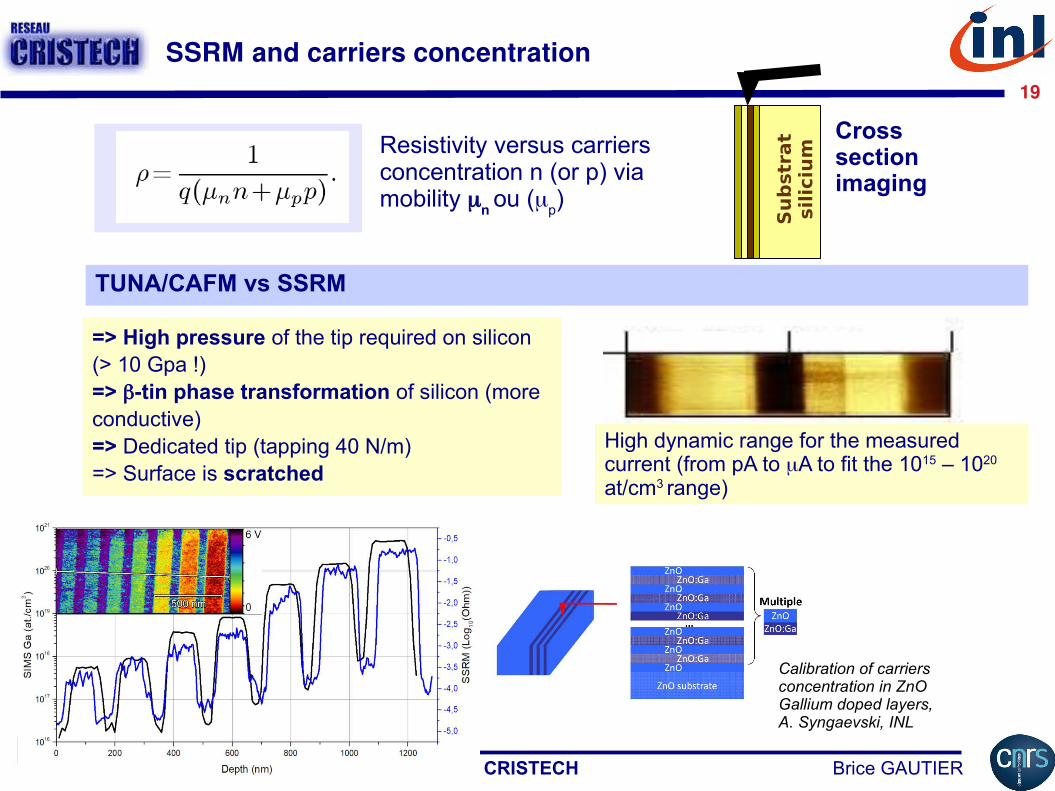
SSRM and carriers concentration
Resistivity versus carriers concentration n (or p) via mobility m
n ou (m
p)
=> High pressure of the tip required on silicon (> 10 Gpa !) => b-tin phase transformation of silicon (more conductive)=> Dedicated tip (tapping 40 N/m)=> Surface is scratched
High dynamic range for the measured current (from pA to mA to fit the 1015 – 1020 at/cm3 range)
TUNA/CAFM vs SSRM
Su
bstr
at
silic
ium
Cross section imaging
A. Syngaevski, INL
Calibration of carriers concentration in ZnO Gallium doped layers, A. Syngaevski, INL
CRISTECH Brice GAUTIEROctobre 2020
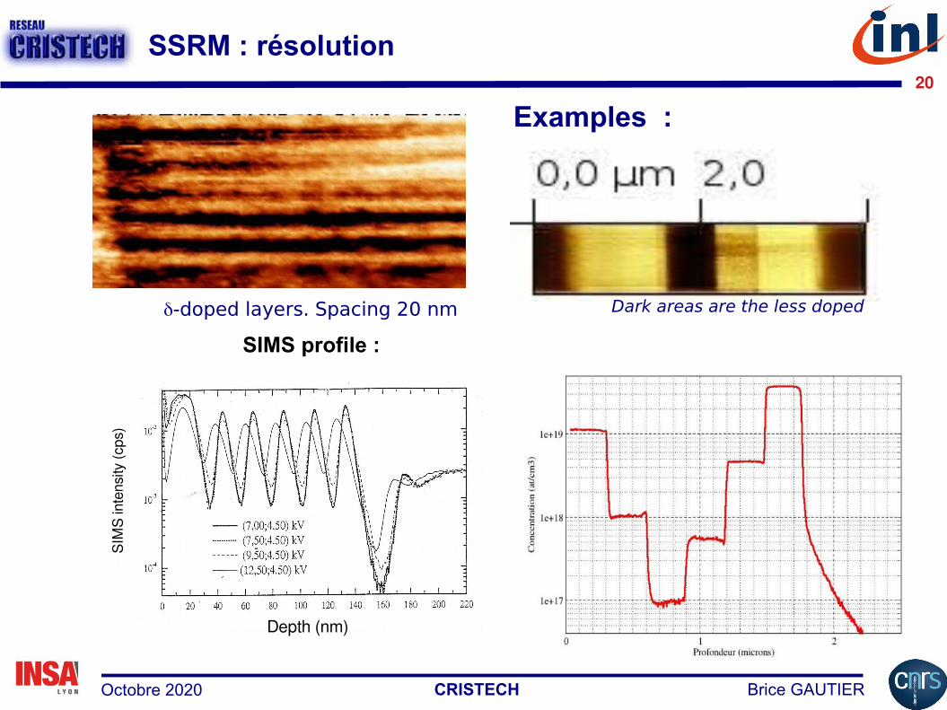
20
d-doped layers. Spacing 20 nm
SSRM : résolution
Examples :
SIMS profile :
Dark areas are the less doped
Depth (nm)
SIM
S in
tens
ity (
cps)
CRISTECH Brice GAUTIEROctobre 2020
21
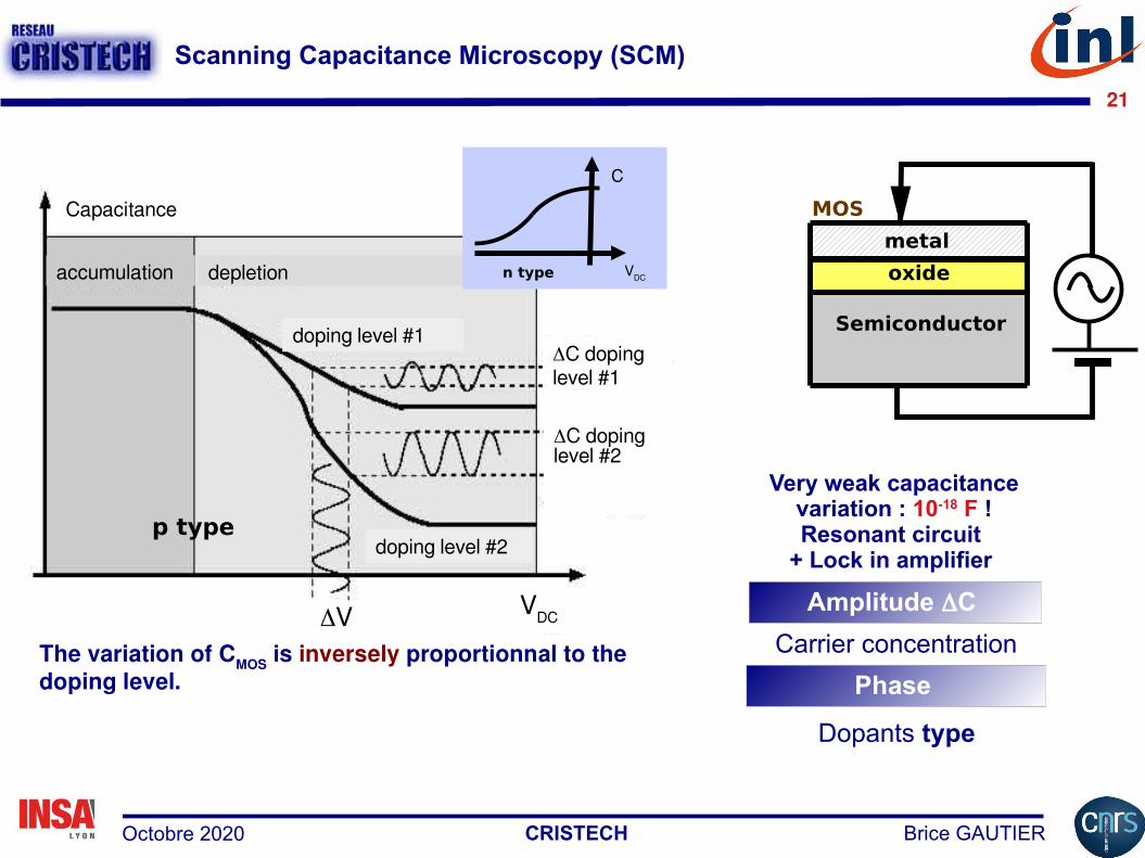
Scanning Capacitance Microscopy (SCM)
ΔC doping level #1
depletionaccumulation
Capacitance
doping level #1
doping level #2
VDCΔV
Semiconductor
metal
MOS
oxide
ΔC doping level #2
VDC
C
n type
p type
The variation of CMOS
is inversely proportionnal to the doping level. Phase
Amplitude ΔC
Carrier concentration
Dopants type
Very weak capacitance variation : 10-18 F !Resonant circuit
+ Lock in amplifier
CRISTECH Brice GAUTIEROctobre 2020
22
VDC
C
type n VDC
C
type p
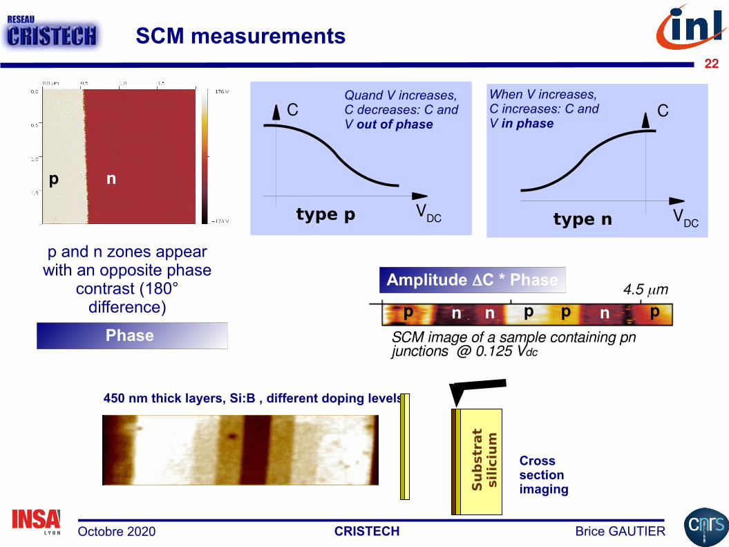
SCM measurements
p n
p and n zones appear with an opposite phase
contrast (180° difference)
Quand V increases, C decreases: C and V out of phase
When V increases, C increases: C and V in phase
Phase
Amplitude ΔC * Phase
SCM image of a sample containing pn junctions @ 0.125 Vdc
4.5 mmnp p n pp n p
450 nm thick layers, Si:B , different doping levels
Su
bstr
at
silic
ium
Cross section imaging
CRISTECH Brice GAUTIEROctobre 2020
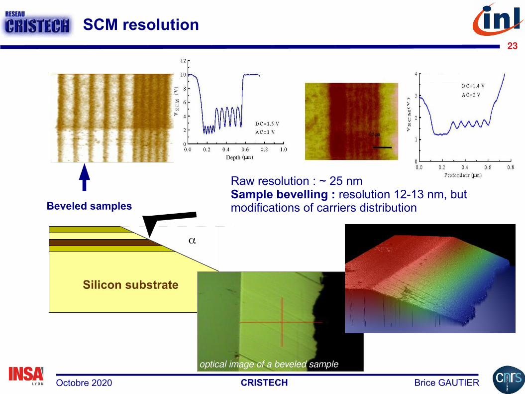
23
SCM resolution
Beveled samples
Silicon substrate
a
Raw resolution : ~ 25 nmSample bevelling : resolution 12-13 nm, but modifications of carriers distribution
optical image of a beveled sample
CRISTECH Brice GAUTIEROctobre 2020
24
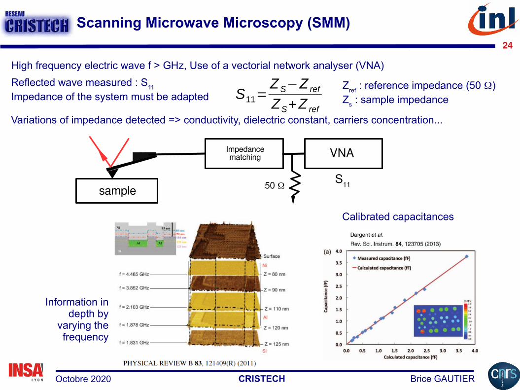
Scanning Microwave Microscopy (SMM)
High frequency electric wave f > GHz, Use of a vectorial network analyser (VNA)
Reflected wave measured : S11
Impedance of the system must be adapted
Variations of impedance detected => conductivity, dielectric constant, carriers concentration...
S11=ZS−Z ref
ZS+Z ref
Zref
: reference impedance (50 W)Z
s : sample impedance
VNAImpedance matching
S11
sample 50 W
Information in depth by
varying the frequency
Calibrated capacitances

CRISTECH Brice GAUTIEROctobre 2020
25
Caracterisation of ferroelectric and piezoelectric materials
CRISTECH Brice GAUTIEROctobre 2020
26
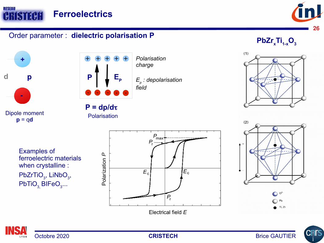
Ferroelectrics
Examples of ferroelectric materials when crystalline :
PbZrTiO3, LiNbO
3,
PbTiO3,
BIFeO3...
Order parameter : dielectric polarisation P
+
-
p
P = dp/dtDipole moment
p = qdPolarisation
d
+ + +++
- - - - -
P EP
Polarisation charge
Ep : depolarisation
field
PbZrxTi
1-xO
3
CRISTECH Brice GAUTIEROctobre 2020
27
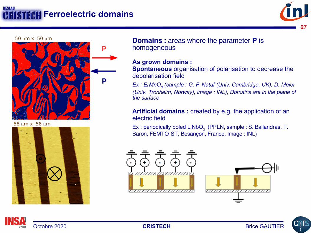
Ferroelectric domains
Domains : areas where the parameter P is homogeneous
As grown domains : Spontaneous organisation of polarisation to decrease the depolarisation fieldEx : ErMnO
3 (sample : G. F. Nataf (Univ. Cambridge, UK), D. Meier
(Univ. Tronheim, Norway), image : INL), Domains are in the plane of the surface
Artificial domains : created by e.g. the application of an electric field Ex : periodically poled LiNbO
3 (PPLN, sample : S. Ballandras, T.
Baron, FEMTO-ST, Besançon, France, Image : INL)
P
P
50 mm x 50 mm
58 mm x 58 mm
CRISTECH Brice GAUTIEROctobre 2020
28
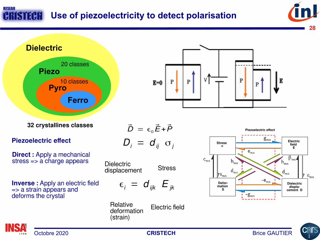
Use of piezoelectricity to detect polarisation
Piezo
Pyro
Ferro
20 classes
10 classes
Dielectric
D i = d ij σ j
Dielectric displacement Stress
Relative deformation (strain)
Electric field
Direct : Apply a mechanical stress => a charge appears
Inverse : Apply an electric field => a strain appears and deforms the crystal
Piezoelectric effect
Piezoelectric effect
Stress σ
Electric field
E
Dielectric displa-
cement D
Defor-mation
S
D⃗ = ϵ0 E⃗ +P⃗32 crystallines classes
ϵi = d ijk E jk
CRISTECH Brice GAUTIEROctobre 2020
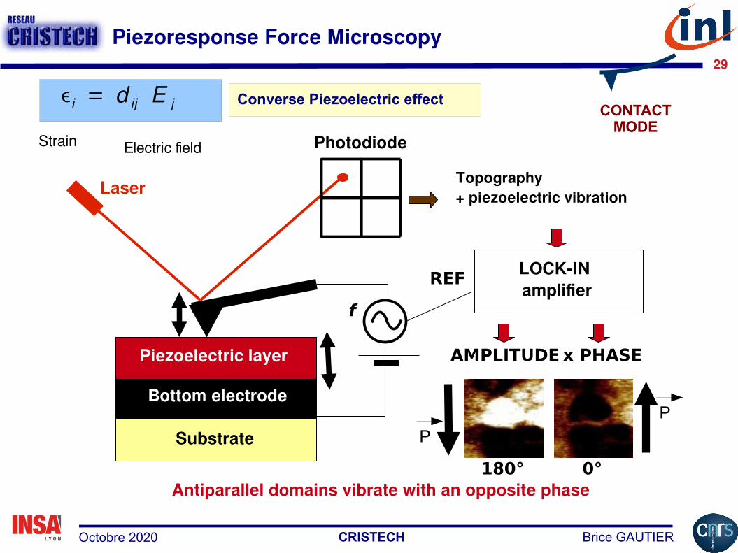
29
Piezoelectric layer
Bottom electrode
Substrate
Photodiode
Topography + piezoelectric vibration
Laser
LOCK-IN amplifier
REF
AMPLITUDE x PHASE
180° 0°
f
P
P
Antiparallel domains vibrate with an opposite phase
Piezoresponse Force Microscopy
Strain Electric field
Converse Piezoelectric effectCONTACT
MODE
ϵi = d ij E j
CRISTECH Brice GAUTIEROctobre 2020
30
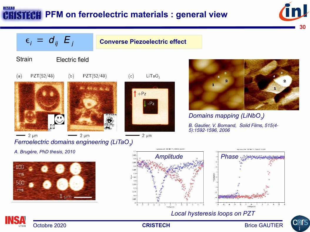
PFM on ferroelectric materials : general view
Strain Electric field
Converse Piezoelectric effect
Ferroelectric domains engineering (LiTaO3)
A. Brugère, PhD thesis, 2010
Domains mapping (LiNbO3)
B. Gautier, V. Bornand, Solid Films, 515(4-5):1592-1596, 2006
Local hysteresis loops on PZT
Amplitude Phase
ϵi = d ij E jϵi = d ij E j
Recommended