Embed Size (px)
Citation preview
Joel Pedro Peixoto de Carvalho
Optical Switching Techniques:
Device Development and Implementation
in Fibre Optic Technology
Thesis submitted to Faculdade de Engenharia da Universidade do Porto
in partial fulfilment of the requirements for the degree of Master in Engenharia Electrotecnica e de Computadores
Departamento de Engenharia Electrotécnica e de Computadores Faculdade de Engenharia da Universidade do Porto
2007


Thesis supervised by
PhD Henrique Manuel de Castro Faria Salgado Associate Professor of Departamento de Engenharia Electrotécnica e de Computadores of
Faculdade de Engenharia da Universidade do Porto


In memory of my grandfather Berto
To my parents and my brother Paulo
To my fiancée Raquel

7
Acknowledgements
First I would like to thank Prof. Henrique Salgado for giving me the opportunity, in 2002, to
work with him at INESC Porto - Opoelectronics and Electronic Systems Unit (UOSE). This made
me understand what research really was. I would also like to thank his support advice and
suggestions as my dissertation supervisor.
I also would like to thank Orlando Frazão for his ideas, the provided motivation, his ‘optics
feelings’, optimism and encouragement at all times.
I would like to thank Igor Terroso and Rosa Romero, without them this work would have
been very hard to accomplish.
I can’t forget Prof. José Luís Santos, UOSE’s manager, and its tremendous professional and
personal qualities. Thank you, Professor for your advices and guidance.
I have to thank the big UOSE family, and the good working atmosphere we had together.
Thank you Luísa Mendonça, Paulo Caldas, Ireneu Dias, Susana Silva, Diana Viegas, Paulo Marques,
Dionísio Pereira, Pedro Jorge, Manuel Joaquim, Miguel Melo, Luís Gomes, Paulo Moreira, Gaspar
Rego and Rui Morais.
Finally I want to thank my fiancée Raquel, my parents and my brothers for their love, support
and patience all these years. I am sorry for the quality time I took away from you.
Many and truly thanks to all of you!
Sincerely yours,
Joel Pedro Carvalho

8
9
Abstract
Optical switching is a fundamental functionality in next generation optical networks to answer
to ever growing bandwidth demand in modern communication networks. This dissertation aims to
present a study about optical switching technologies as also a development and implementation
work of all-optical switching devices.
Among the many present day technologies, two different techniques were studied and
implemented. The first one was based in the tuneability of fibre Bragg grating and the second one
recurs to nonlinear optics.
Fine tuning of fibre Bragg gratings can be accomplished through temperature variation or
longitudinal mechanical deformation. Four distinct architectures that use these techniques will be
presented in this dissertation.
Another alternative is the used of wavelength conversion to achieve switching. Wavelength
conversion in this context is discussed based on four-wave mixing in the optical fibre. In this
dissertation two techniques are also presented, based on the use of special fibres, to generate the
four wave mixing non linear effect.
Based on the previously studied techniques, two types of key devices in optical
communication networks were implemented and their performance is presented, namely, an
“Optical Add-Drop Multiplexer” and an “Optical Cross-Connect”. Finally, the scalability of the
latter device is discussed.

11
Resumo
A comutação óptica é uma funcionalidade fundamental nas redes ópticas de próxima geração
para responder aos crescentes requisitos de largura de banda nas modernas redes de comunicação.
Esta dissertação apresenta um estudo sobre tecnologias de comutação bem como um trabalho de
desenvolvimento e implementação de dispositivos para comutação totalmente óptica.
Entre as muitas tecnologias conhecidas actualmente, foram especificamente estudadas e
implementadas duas técnicas diferentes. A primeira é baseada na sintonia de redes de Bragg em fibra
e a segunda recorrendo a óptica não linear.
A sintonia de redes de Bragg em fibra óptica pode ser obtida através da variação da
temperatura ou recorrendo à aplicação de deformação mecânica longitudinal. Nesta dissertação
quatro arquitecturas distintas recorrendo a estas técnicas de comutação são apresentadas.
Outra alternativa é o recurso à conversão de comprimento de onda para obter a comutação
óptica. A conversão de comprimento de onda é neste contexto discutida baseada no processo de
mistura de quatro ondas em fibra óptica. Nesta tese duas técnicas, baseadas no uso de fibras ópticas
especiais, para geração do efeito não linear de mistura de quatro ondas são também apresentadas.
Com base nas técnicas estudadas, dois tipos de dispositivos chave nas redes de comunicação
óptica, foram implementados e a sua performance avaliada, nomeadamente, um “Optical Add-Drop
Multiplexer” e um “Optical Cross-Connect”. Finalmente a escalabilidade do último dispositivo foi
discutida.

12
13
Contents
Acknowledgements...................................................................................................................................... 7 Abstract ......................................................................................................................................................... 9 Resumo........................................................................................................................................................ 11 Contents ...................................................................................................................................................... 13 List of Figures............................................................................................................................................. 17
1 Introduction.........................................................................................................................21 1.1 Background and Thesis Motivation............................................................................................. 21 1.2 Thesis Structure .............................................................................................................................. 21 1.3 Contributions .................................................................................................................................. 22 1.4 List of publications......................................................................................................................... 22
2 Optical Networks ................................................................................................................27 2.1 Introduction .................................................................................................................................... 27 2.2 Evolution of Optical Networks ................................................................................................... 27 2.3 Optical time division multiplexing............................................................................................... 29 2.4 Optical code division multiplexing .............................................................................................. 29 2.5 Wavelength division multiplexing................................................................................................ 30
2.5.1 WDM link.................................................................................................................................. 31 2.5.2 Passive optical networks.......................................................................................................... 32 2.5.3 Broadcast and select networks................................................................................................ 32 2.5.4 Wavelength routed networks .................................................................................................. 33 2.5.5 Photonic packet switching networks ..................................................................................... 34
2.6 Summary.......................................................................................................................................... 35 3 Optical Switching – State of the art.....................................................................................37
3.1 Introduction .................................................................................................................................... 37 3.2 All optical switching approaches.................................................................................................. 37 3.3 Optical switch fabrics .................................................................................................................... 38
3.3.1 Optomechanical Switches ....................................................................................................... 38 3.3.2 Micro-Optical-Mechanical-Systems Switches....................................................................... 39 3.3.3 Electro-optic Switches ............................................................................................................. 41 3.3.4 Thermo-optic Switches............................................................................................................ 41 3.3.5 Liquid-Crystal Switches ........................................................................................................... 42 3.3.6 Bubble Switches........................................................................................................................ 43 3.3.7 Acousto-optic Switches ........................................................................................................... 44 3.3.8 Semiconductor Optical Amplifiers Switches........................................................................ 44 3.3.9 Fibre Bragg granting based Switches ..................................................................................... 45
3.4 Example of applications................................................................................................................ 45 3.5 Wavelength-domain routers ......................................................................................................... 47 3.6 Summary.......................................................................................................................................... 48
4 Fibre Bragg Gratings Technology ......................................................................................49 4.1 Introduction .................................................................................................................................... 49 4.2 Bragg diffraction............................................................................................................................. 49
14
4.3 Photosensitivity .............................................................................................................................. 50 4.4 Fibre Bragg Gratings fabrication techniques.............................................................................. 51
4.4.1 Interferometric or holographic technique............................................................................. 52 4.4.2 Point-by-point technique......................................................................................................... 53 4.4.3 Phase mask Technique............................................................................................................. 53 4.4.4 Amplitude mask technique...................................................................................................... 54 4.4.5 FBG spectral response............................................................................................................. 56 4.4.6 Coupled Mode Theory............................................................................................................. 58 4.4.7 Different kinds of FBG........................................................................................................... 59
4.5 Bragg gratings sensitivity to strain and temperature ................................................................. 61 4.6 Applications of fibre gratings ....................................................................................................... 62 4.7 Summary.......................................................................................................................................... 63
5 Nonlinear effects for optical switching...............................................................................65 5.1 Introduction .................................................................................................................................... 65 5.2 Wavelength conversion ................................................................................................................. 65
5.2.1 Optoelectronic Wavelength Converters................................................................................ 66 5.2.2 Optical Gating Wavelength Converters ................................................................................ 66 5.2.3 Wave-Mixing Wavelength Converters................................................................................... 66
5.3 Optoelectronic wavelength conversion ...................................................................................... 67 5.4 Optical gating.................................................................................................................................. 68
5.4.1 Cross-gain modulation in SOAs............................................................................................. 69 5.4.2 Cross-phase modulation in SOAs.......................................................................................... 70 5.4.3 Semiconductor with saturable absorption wavelength converter...................................... 72 5.4.4 Non-linear optical loop mirror wavelength converter ........................................................ 72
5.5 Wave Mixing Wavelength Conversion........................................................................................ 73 5.5.1 Four wave mixing in SOAs ..................................................................................................... 74 5.5.2 Difference frequency generation............................................................................................ 75 5.5.3 Four wave mixing on optical fibres ....................................................................................... 75
5.6 Optical fibre four-wave mixing theory........................................................................................ 75 5.6.1 Non-degenerated four-wave mixing ...................................................................................... 76 5.6.2 Degenerated four wave mixing............................................................................................... 78 5.6.3 Four Wave Mixing process and conversion efficiencies..................................................... 79 5.6.4 Degenerated vs. Non-degenerated four wave mixing.......................................................... 81
5.7 Summary.......................................................................................................................................... 82 6 Experimental studies in optical switching and wavelength conversion ............................83
6.1 Introduction .................................................................................................................................... 83 6.2 Fibre Bragg gratings based optical switching techniques ......................................................... 83 6.3 Thermal effects based optical switching ..................................................................................... 84
6.3.1 FBG tuning through a Peltier element .................................................................................. 84 6.3.2 FBG tuning through a thin film ............................................................................................. 86 6.3.3 FBG tuning through a pump laser diode .............................................................................. 88
6.4 Mechanical effects based optical switching ................................................................................ 92 6.5 Conclusions on FBG based switching techniques .................................................................... 94 6.6 Wavelength conversion techniques ............................................................................................. 94
6.6.1 Wavelength conversion scheme based in a ring erbium doped fibre laser ...................... 94 6.6.2 Wavelength conversion scheme based in a Photonic Crystal Fibre.................................. 99
6.7 Conclusions on wavelength conversion schemes.................................................................... 102 6.8 Splicing PCFs with SMFs for wavelength conversion purposes........................................... 102
15
6.8.1 Experimental results............................................................................................................... 103 6.8.2 Conclusions on splicing issues.............................................................................................. 106
6.9 Summary........................................................................................................................................ 106 7 Development of optical network elements ....................................................................... 107
7.1 Introduction .................................................................................................................................. 107 7.2 Optical add-drop multiplexers.................................................................................................... 107
7.2.1 Experimental implementation of an OADM..................................................................... 107 7.3 Optical cross-connects ................................................................................................................ 111
7.3.1 Experimental implementation of an OXC ......................................................................... 111 7.3.2 OXC bidirectionality and scalability capabilities ................................................................ 116
7.4 Summary........................................................................................................................................ 118 8 Concluding remarks .......................................................................................................... 121 Appendix 1 – Conversor de comprimento de onda baseado num laser em fibra óptica....... 123 Appendix 2 – Router Óptico para sistemas DWDM com selectividade e conversão de comprimento de onda............................................................................................................ 137 Bibliography........................................................................................................................... 155

17
List of Figures
Figure 2.1 - Three generations of networks. [3].......................................................................................... 28
Figure 2.2 - The bandwidth of single mode optical fibres defined by the zones of low attenuation . 29
Figure 2.3 - OTDM approach to achieve 40 Gbit/s in the fibre using the same wavelength............. 29
Figure 2.4 - Wavelength Division Multiplexing .......................................................................................... 30
Figure 2.5 - Schematic of the WDM concept ............................................................................................. 31
Figure 2.6 – WDM link architecture............................................................................................................. 31
Figure 2.7 – Broadcast-and-select WDM networks: (a) star topology; (b) bus topology. .................... 33
Figure 2.8 – Wavelength routing network ................................................................................................... 34
Figure 3.1 - Two-axis tilting mirror MEMS (picture from Lucent Technologies) ................................ 39
Figure 3.2 – Two arrays of N tilting mirrors, interconnecting N inputs with N outputs..................... 40
Figure 3.3 – A 2 × 2 electrooptic switc......................................................................................................... 41
Figure 3.4 – 2 × 2 Mach-Zhender inferferometer switch.......................................................................... 42
Figure 3.5 – 2 × 2 digital optical switch ....................................................................................................... 42
Figure 3.6 – Principle of operation of a 1 × 2 liquid-crystal optical switch............................................ 43
Figure 3.7 – Principle of operation of a 2 × 2 bubble switch. (left) bar state; (right) cross state. ....... 43
Figure 3.8 – Schematic of a polarization independent Acousto-optic switch ........................................ 44
Figure 3.9 – N × N SOA based switch in a tree arrangement.................................................................. 45
Figure 3.10 – OADM based on a combination of an FBG and two optical circulators ...................... 45
Figure 3.11 – Crossconnect pattern of a static wavelength router. The device routes signals from an
input to an output based on their wavelength. ................................................................... 47
Figure 3.12 – An arrayed waveguide grating ............................................................................................... 48
Figure 4.1 – Experimental setup for FBG fabrication using an interferometric technique ................. 52
Figure 4.2 – Experimental setup for FBG fabrication using the point-by-point technique ................ 53
Figure 4.3 – Experimental setup for FBG fabrication using the phase mask technique...................... 54
Figure 4.4 – Experimental setup for FBG fabrication using the amplitude mask technique .............. 55
Figure 4.5 – Schematic of a Fibre Bragg Grating operation principle and response ............................ 56
Figure 4.6 – Spectral response of a uniform fibre Bragg grating ............................................................. 59
Figure 4.7 – Spectral response of a apodized fibre Bragg grating............................................................ 60
Figure 4.8 – Optical add-drop multiplexer based in the FBG technology ............................................. 62
Figure 5.1 – All optical switching and packet routing using a fast tuneable wavelength converter.... 65
18
Figure 5.2 – Different types of optoelectronic regeneration. (a) 1R regeneration (without reshaping
and retiming), (b) 2R regeneration with reshaping, (c) 3R regeneration with reshaping
and retiming.............................................................................................................................. 68
Figure 5.3 – XGM wavelength conversion principle: (a) co-propagating signals, (b) counter
propagating signals. ................................................................................................................. 69
Figure 5.4 – Configurations for interferometric wavelength SOA wavelength converter: (a) an
asymmetric MZI, (b) a symmetric MZI, (c) Michelson interferometer (MI). ................ 71
Figure 5.5 – NOLM wavelength converters: (a) fibre loop, (b) SOA as the nonlinear medium......... 73
Figure 5.6 – Schematic of FWM in the frequency domain ....................................................................... 74
Figure 5.7 – Non-degenerated four wave mixing in the frequency domain........................................... 76
Figure 5.8 – Degenerated four wave mixing in the frequency domain ................................................... 76
Figure 6.1 – Experimental setup for thermal tuning of the FBG using a Peltier element ................... 84
Figure 6.2 - Braggλ temperature dependence ............................................................................................. 85
Figure 6.3 – Tuning and detuning time of the optical filter...................................................................... 85
Figure 6.4 – Grating spectrum in several situations................................................................................... 86
Figure 6.5 – Sample behaviour when a 0,1 Hz electrical signal was applied .......................................... 87
Figure 6.6 – Switching results applying different electrical signals to the sample. (left) using a 0.2 Hz
signal current that induces a 1 nm shift in Braggλ ; (right) using a 0.2 Hz signal that
induces a 10nm shift Braggλ .................................................................................................... 88
Figure 6.7 – Electrical power consumption vs. wavelength shift ............................................................. 88
Figure 6.8 – Experimental setup of the all-optical switch......................................................................... 89
Figure 6.9 – Measured dependency of the peak wavelength on the applied pumping power when an
undoped fibre is used.............................................................................................................. 90
Figure 6.10 – Measured reflection spectra, with maximum pumping power (red line) and without
(black line), of the FBG written in a undoped fibre........................................................... 90
Figure 6.11 – Measured dependency of the peak wavelength on the applied pumping power when a
doped fibre is used .................................................................................................................. 91
Figure 6.12 – Measured reflection spectra, with maximum pumping power (red line) and without
(black line), of the FBG written in a doped fibre. .............................................................. 91
Figure 6.13 – Spectral response of the grating when a PZT is used........................................................ 93
Figure 6.14 – Wavelength and power responses of the transducer when the input PZT voltage is
varied. Dots and triangles show the experimental results obtained. In red it can be seen
a linear fit for the optical reflected power. In blue is showed the wavelength response
translated by a second order polynomial fit......................................................................... 93
19
Figure 6.15 – Experimental setup of the all-fibre wavelength converter................................................ 95
Figure 6.16 – Sample of the optical spectra when λ of the input signal is changed. (A–H: input
signal;......................................................................................................................................... 96
Figure 6.17 – Relationship between wavelength of the input signal and the wavelength and power of
the resulting conjugate as the wavelength of the in put signal is changed keeping the
power constant......................................................................................................................... 97
Figure 6.18 – Samples of the optical spectrum of the device when the wavelength of the pump signal
was is changed by application of strain to the FBG........................................................... 97
Figure 6.19 – Relationship between the wavelength of the input power and the resulting conjugate as
the pump signal is changed .................................................................................................... 98
Figure 6.20 – FWM efficiency dependence on separation between input signal and pump signal .... 99
Figure 6.21 – Cross-sectional SEM images of the PCF (NL 2. 3 1555) from Crystal Fibre A/S ....... 99
Figure 6.22 – PCF dispersion characteristic ..............................................................................................100
Figure 6.23 – Experimental setup of the PCF based wavelength converter ........................................100
Figure 6.24 – Measured spectra for different input signals.....................................................................101
Figure 6.25 – Four wave mixing conversion efficiency ...........................................................................101
Figure 6.26 – a) Result of the Fujikura’s splice machine automatic jointing of the fibres (The 25 μm
gap between both fibres is seen). Now the PCF is fixed and the SMF-28TM is moved
on; b) Result of manual alignment (After this, the electric arc is discharged). .............104
Figure 6.27 – Evaluation of arc duration time with a constant current power. ...................................105
Figure 6.28 – Visualization of the SMF-28TM/PCF splice in the Fujikura’s FSM-40S screen. ..........105
Figure 7.1 – Spectral Response of the apodized FBG.............................................................................108
Figure 7.2 – Experimental setup used to evaluate the OADM performance ......................................108
Figure 7.3 – Optical Spectral of the OADM: a) at the IN and the OUT ports; b) at the Drop with
and without the Optical Filter .............................................................................................109
Figure 7.4 – Eye Diagrams: a) Drop with FP Filter; b) Drop without FP Filter.................................110
Figure 7.5 – BER performance of the dropped signal ............................................................................110
Figure 7.6 – a) Three wavelengths input signal. b) Output of the OADM when 2λ is added to the
system when 1λ and 3λ are at the input port.....................................................................111
Figure 7.7 – Eye Diagram of the output of the OADM when 2λ is added to the system when 1λ
and 3λ are at the input port ..................................................................................................111
Figure 7.8 – a) 2 2× FBG-OC based OXC. Three switching states b) bar-state, c) cross-state and d)
simultaneous-state. ................................................................................................................112
Figure 7.9 – Ring architecture for the same 2 2× OXC presented in Figure 7.8................................113

20
Figure 7.10 – Optical spectra obtained at the two output ports a) with FBG tuned b) FBG off-
tuned........................................................................................................................................114
Figure 7.11 – Crosstalk level measurement using FBGs with a) uniform and b) apodized spectral
profiles.....................................................................................................................................115
Figure 7.12 – Proposed architecture of bi-directional OXC based in 2 2× OXC..............................116
Figure 7.13 – The rearrangeably 4 4× optical cross-connect constructed by using 2 2× OXC .........117
Figure 7.14 – Number of required OCs and FBGs series in order to the 2 2× OXC dimension ...118
1 Introduction
1.1 Background and Thesis Motivation
Internet-based services are driving the need for evermore bandwidth in the new generation
networks, consequently communications must evolve to sustain such a demand. All optical
networks (AONs), based on the Wavelength Division Multiplexing (WDM) technologies, are
very often considered to be the main candidate for constituting the backbone that will carry
global data traffic in the near future. In AONs, each connection, i.e. each lightpath, is totally
optical, and totally transparent, so a connection doesn’t need to be interrupted by any optical-
electrical conversion. Optical switches are network elements that will play a key role in WDM
networks to provide more reconfiguration flexibility and network survivability , hence the need
for the study of practical techniques for the implementation of such switches and optical
switching technology. In particular, the fibre Bragg grating is a potential candidate with great
interest in optical switching applications.
Fibre Bragg gratings are optical filters that formed through a modulation of the fibre core
refractive index which is obtained after exposure to ultraviolet radiation. There are a enormous
number of different FBGs applications in sensors and optical communications. In this work we
focus the FBGs tuneability capabilities and their consequent applications in optical switching.
Optical wavelength converters are also important optical network devices that rely on
nonlinear optics technology and that could improve optical switching network capabilities.
Optical cross-connects (OXCs) and optical add-drop multiplexers (OADMs) are optical
switches that can interconnect optical signals between multiple input and output ports, enabling
switching and routing capabilities. Although, those devices are used for adding, removing and
switching light paths they could also rely in Bragg grating technology.
1.2 Thesis Structure
The thesis is divided in eight chapters as follows:
⎯ Chapter 1 gives the motivation and the thesis description.
⎯ Chapter 2 gives a general description of the evolution of the optical networks as also an
extended discussion of the wavelength division multiplexing technique and its future.
⎯ Chapter 3 gives an extensive description of the optical switching technology state of
the art and his network applications.
22
⎯ Chapter 4 describes the fibre Bragg gratings technology. A general description of the
FBGs fabrication techniques is made. A brief theoretical approach through the coupled mode
theory is also done. Finally the FBGs sensitivity to strain and temperature is mentioned as also
some applications to optical switching.
⎯ Chapter 5 shows how wavelength conversion is so important in the new optical
networks concept. Different kinds of wavelength conversion techniques are described with
special attention to the four wave-mixing approach.
⎯ Chapter 6 presents the experimental study of the FBGs behaviour in several optical
switching concepts. Different kinds of thermal and mechanical optical switching are tested. Two
different wavelength converters are tested.
⎯ Chapter 7 explains the principal characteristics (with a particular emphasis in crosstalk)
of an implementation of a optical add-drop multiplexing and an optical cross-connect.
⎯ Chapter 8 concludes the thesis with a discussion of the obtained results. Future work
suggestions are also given.
1.3 Contributions
1. FBG tuning through a Peltier element
2. FBG tuning through a thin film
3. FBG tuning through a pump laser diode
4. FBG tuning through a mechanical switch
5. Wavelength conversion scheme based in a ring erbium doped fibre laser
6. Splicing between a photonic crystal fibre and a single mode fibre
7. Wavelength conversion traditional scheme based in a photonic crystal fibre
8. Optical add-drop multiplexer experimental implementation
9. Optical cross-connect development
1.4 List of publications
Patents
O. Frazão, J. P. Carvalho, I. Terroso, H. M. Salgado, “Router Óptico para sistemas DWDM
com selectividade e conversão de comprimento de onda”, PT, Portuguese Patent in Instituto
Nacional da Propriedade Industrial, N. 102982, 27 Junho 2003.
23
O. Frazão, J. P. Carvalho, I. Terroso, H. M. Salgado, “Conversor de Comprimento de Onda
Baseado Num Laser em Fibra Óptica”, PT, Portuguese Patent in Instituto Nacional da
Propriedade Industrial, N. 102983, 27 Junho 2003.
Papers in Journals
O. Frazão, I. Terroso, J. P. Carvalho, H. M. Salgado, “Optical cross-connect based on
tuneable FBG-OC with full scalability and bidirectionality”, Optics Communications, Volume
220, Issues 1-3, pp. 105-109, 1 May, 2003.
I. Terroso, J. P. Carvalho, O. Frazão, M. B. Marques, H. M. Salgado, “All-Fibre Wavelength
Conversion based on Four-Wave-Mixing in a Ring Erbium Doped Fibre Laser”, Applied Physics
B: Lasers and Optics, Springer-Verlag, Volume 77, pp. 133-137, 2003.
J. P. Carvalho, R. Romero, M. Melo, L. A. Gomes, O. Frazão, M. B. Marques, H. M.
Salgado, “Optical Fibre Communications: Recent Contributions in Optical Device Technology”,
Fiber & Integrated Optics (Invited Paper), Volume 24, Issues 3-4, pp.371-394, May-August 2005.
O. Frazão, J. P. Carvalho, H. M. Salgado “Low loss splice in a Photonic Crystal Fiber using a
Conventional Fusion Splicer”, Microwave and Optical Technology Letters, Volume 46, Issue 2,
pp. 172-174, 20 July 2005.
J. P. Carvalho, O. Frazão, R. Romero, M. B. Marques, H. M. Salgado, “Fibre Bragg Grating
switching behaviour using high power laser diodes”, Microwave and Optical Technology Letters,
Vol. 48, No. 8, pp. 1538-1540, August 2006
Papers published in international conferences
O. Frazão, J.P. Carvalho, I. Terroso, V. Barbosa, H.M. Salgado, “A Novel Architecture of an
Optical Cross-connect Based on Tuneable Fibre Bragg Gratings and Optical Circulators”,
London Communication Symposium 2002, LCS 2002, September 2002.
J. P. Carvalho, I. Terroso, R. Romero, O. Frazão, P. S. André, “Performance Evaluation of
an Optical Add Drop Multiplexer using an apodized Bragg Grating”, I Symposium on Enabling
Optical Networks, I Site-On, Enabling Technologies for All-Optical Networks, Instituto de
Telecomunicações, Aveiro, Portugal, 17 Junho 2003.
I. Terroso, C. C. Mardare, A. I. Mardare, J. P. Carvalho, O. Frazão, E. Joanni, “Tunable
Thin-film-heated fiber Bragg grating”, I Symposium on Enabling Optical Networks, I Site-On,
Enabling Technologies for All-Optical Networks, Instituto de Telecomunicações, Aveiro,
Portugal, 17 Junho 2003.
24
J. P. Carvalho, I. Terroso, O. Frazão, H. M. Salgado, “Optical Cross-connect Architectures
based on Fibre Bragg Gratings and Optical Circulators”, ConfTele 2003, 4th Conference on
Telecommunications, Aveiro – Portugal, 6–8 June, 2003.
I. Terroso, J. P. Carvalho, O. Frazão, H. M. Salgado, “Wavelength Conversion based on
Four-Wave-Mixing in a Ring Laser”, London Communication Symposium 2003, LCS 2003,
September 2003.
A. P. Almeida, F. S. Pinto, D. J. Barros, J. P. Carvalho, O. Frazão, P. S. André, H. M.
Salgado, “Non-linear Effects in Photonic Crystal Fibres”, II Symposium on Enabling Optical
Networks – Celebrating 10 years of fibre bragg gratings in portugal, SEON 2004, June 14th,
Porto, 2004.
F. S. Pinto, D.J. Barros, A. P. Almeida, J. P. Carvalho, O. Frazão, H. M. Salgado,
“Wavelength Conversion Efficiency in a Dispersion Shifted Fibre”, II Symposium on Enabling
Optical Networks – Celebrating 10 years of fibre bragg gratings in portugal, SEON 2004, June
14th, Porto, 2004.
D. J. Barros, A. P. Almeida, F. S. Pinto, J. P. Carvalho, O. Frazão, H. M. Salgado, “Four-
Wave Mixing in Photonic Crystal Fibres for Wavelength Conversion in Optical Networks”,
London Communication Symposium 2004, LCS 2004, 13th-14th September 2004.
J. P. Carvalho, R. Romero, O. Frazão, M. B. Marques, “All-optical switching in a Bragg
grating structure using a high power laser diode”, III Symposium on Enabling Optical Networks,
SEON 2005, June 27th, Aveiro, 2005.
J. P. Carvalho, O. Frazão, R. Romero, M. B. Marques, H. M. Salgado, “Fibre Bragg Grating
switching based on thermal changes induced by high power laser diodes”, SEON 2006 – VI
Symposium on Enabling Optical Networks and Sensors, pp. 59-60, Porto, June 16th, 2006
J. P. Carvalho, M B. Marques, “Aumento do limiar do espalhamento estimulado de Brillouin
em fibra por modulação em temperatura”, 15.ª Conferencia Nacional de Física, Física 2006, 4-7
Setembro, Aveiro, 2006.
Papers published in national conferences
J. P. Carvalho, O.Frazão, R. Romero, M. B. Marques, H. M. Salgado, “Técnicas e
arquitecturas de comutação totalmente óptica em redes de multiplexagem densa por
comprimento de onda”, Terceiras Jornadas de Engenharia de Electrónica e Telecomunicações e
de Computadores, JETC 05, 17-18 November, Lisboa, 2005.
O. Frazão, J. P. Carvalho, H. M. Salgado, J. L. Santos, L. A. Ferreira, F. M. Araújo, “Fibras
ópticas microestruturadas e suas aplicações em sensores e telecomunicações”, XIV Conferencia
25
da Sociedade Portuguesa de Física, Física 2005 – Física para o Século XXI, 1-3 December, Porto,
2005.
Frazão, J. P. Carvalho, R. Romero, F. M. Araújo, L. A. Ferreira, H. M. Salgado, M. B.
Marques, J. L. Santos, “Redes de bragg em fibra óptica e suas aplicações como elementos
sensores e em comunicações ópticas”, XIV Conferencia da Sociedade Portuguesa de Física,
Física 2005 – Física para o Século XXI, 1-3 December, Porto, 2005.
J. P. Carvalho, O. Frazão, R. Romero, M. B. Marques, H. M. Salgado, “Fibre gratings
switching behaviour based on high power laser diodes”, 15.ª Conferencia Nacional de Física,
Física 2006, 4-7 Setembro, Aveiro, 2006.

2 Optical Networks
2.1 Introduction
The recent Internet explosion verifies the needs for much larger communication capacity. To
meet such requirements, optical networks are evolving and new technologies and networks
configurations are being studied in order to sustain the enormous growth in the demand of
bandwidth. In this chapter a brief introduction on the evolution of optical networks is given in
section 2.2 and a description of the different channel concurrency techniques employed in such
networks is carried out from sections 2.3 to 2.5. Finally, particular emphasis is given to wavelength
division multiplexing technique and its typical architectures. In sections 2.5.4 and 2.5.5, the evolution
of WDM towards wavelength routed networks and the optical packet switching is discussed.
2.2 Evolution of Optical Networks
Over the past few years, the field of computer and telecommunications networking has
experienced tremendous growth. With the rapidly growing popularity of the Internet and computer
networks, this growth can be expected to continue in the foreseeable future. All-optical networks are
those in which the path between the network nodes remains entirely optical from end to end. Such
paths are termed lightpaths. Each lightpath may be optically amplified or have its wavelength altered
along the way, either way it is a purely optical path. As the optoelectronic technology to build optical
networks has gotten closer to functional and economic feasibility, more and more groups worldwide
are studying them as a possible base upon which to build the networks of the future, both within the
wide area backbone and for metropolitan and local area distribution facilities. In view of the
potential and recent advances in optical networks, all-optical networks are the main candidate for
constituting the backbone that will carry the global data traffic whose volume has been growing at
outstanding rates that are not expected to slow down in the near future.
According to the physical technology employed, one can identify three generations of
networks (Figure 2.1). Networks built before the emergence of optical fibre technology are the first
generation networks, i.e., networks based on copper wire or radio. The second generation networks
employ fibres in traditional architectures. The choice of fibre is due to its large bandwidth, low error
rate, reliability, availability, and maintainability. Although performance improvements can be
achieved by employing fibres, the performance for this generation is limited by the maximum speed
of electronics (a few gigabits per second) employed in switches and end-nodes. This phenomenon is
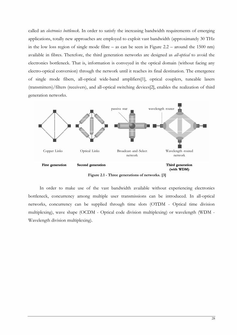
28
called an electronics bottleneck. In order to satisfy the increasing bandwidth requirements of emerging
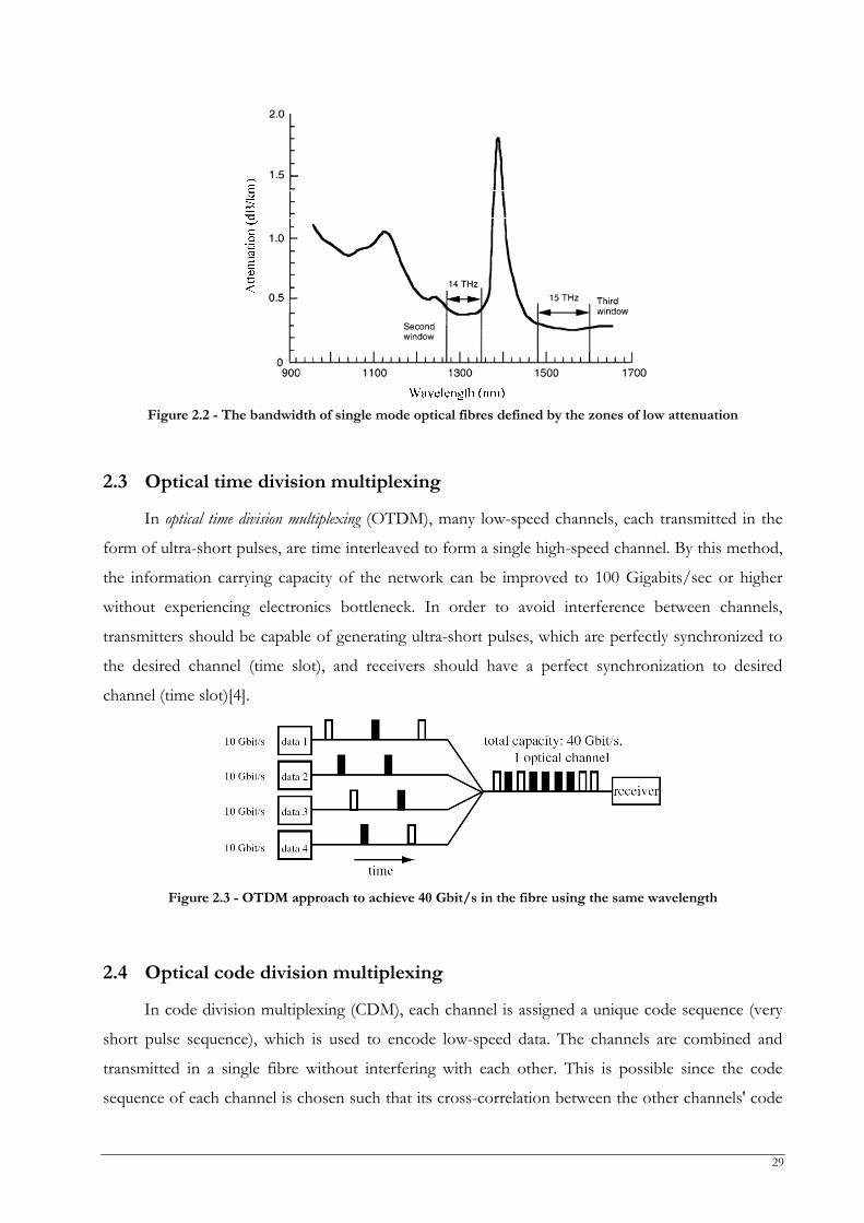
applications, totally new approaches are employed to exploit vast bandwidth (approximately 30 THz
in the low loss region of single mode fibre – as can be seen in Figure 2.2 – around the 1500 nm)
available in fibres. Therefore, the third generation networks are designed as all-optical to avoid the
electronics bottleneck. That is, information is conveyed in the optical domain (without facing any
electro-optical conversion) through the network until it reaches its final destination. The emergence
of single mode fibers, all-optical wide-band amplifiers[1], optical couplers, tuneable lasers
(transmitters)/filters (receivers), and all-optical switching devices[2], enables the realization of third
generation networks.
Copper Links Optical Links Broadcast -and-Selectnetwork
Wavelength - routednetwork
First generation Second generation Third generation (with WDM)
passive star wavelength router
Copper Links Optical Links Broadcast -and-Selectnetwork
Wavelength - routednetwork
First generation Second generation Third generation (with WDM)
passive star wavelength router
Figure 2.1 - Three generations of networks. [3]
In order to make use of the vast bandwidth available without experiencing electronics
bottleneck, concurrency among multiple user transmissions can be introduced. In all-optical
networks, concurrency can be supplied through time slots (OTDM - Optical time division
multiplexing), wave shape (OCDM - Optical code division multiplexing) or wavelength (WDM -
Wavelength division multiplexing).
29
Figure 2.2 - The bandwidth of single mode optical fibres defined by the zones of low attenuation
2.3 Optical time division multiplexing
In optical time division multiplexing (OTDM), many low-speed channels, each transmitted in the
form of ultra-short pulses, are time interleaved to form a single high-speed channel. By this method,
the information carrying capacity of the network can be improved to 100 Gigabits/sec or higher
without experiencing electronics bottleneck. In order to avoid interference between channels,
transmitters should be capable of generating ultra-short pulses, which are perfectly synchronized to
the desired channel (time slot), and receivers should have a perfect synchronization to desired
channel (time slot)[4].
Figure 2.3 - OTDM approach to achieve 40 Gbit/s in the fibre using the same wavelength
2.4 Optical code division multiplexing
In code division multiplexing (CDM), each channel is assigned a unique code sequence (very
short pulse sequence), which is used to encode low-speed data. The channels are combined and
transmitted in a single fibre without interfering with each other. This is possible since the code
sequence of each channel is chosen such that its cross-correlation between the other channels' code
30
sequences is small, and the spectrum of the code sequence is much larger than the signal bandwidth.
Therefore, it is possible to have an aggregate network capacity beyond the speed limits of
electronics. Like OTDM, CDM requires short pulse technology, and synchronization to one chip
time for detection[5].
2.5 Wavelength division multiplexing
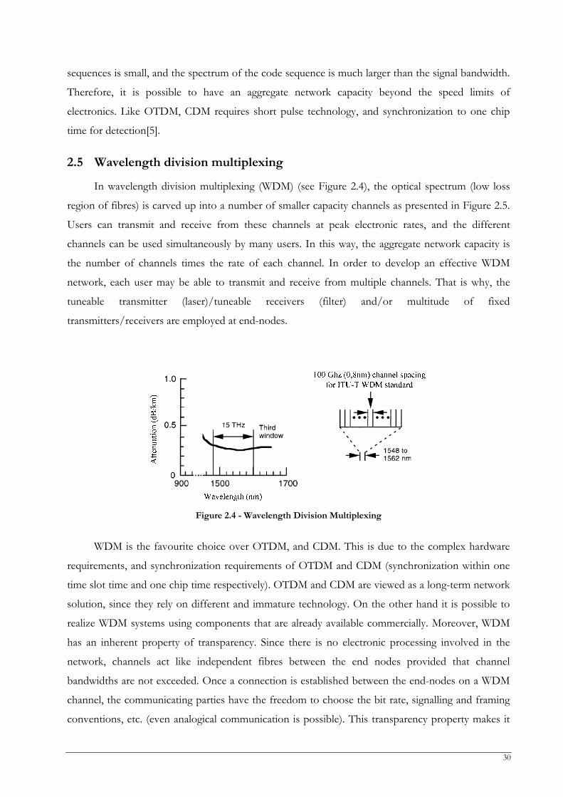
In wavelength division multiplexing (WDM) (see Figure 2.4), the optical spectrum (low loss
region of fibres) is carved up into a number of smaller capacity channels as presented in Figure 2.5.
Users can transmit and receive from these channels at peak electronic rates, and the different
channels can be used simultaneously by many users. In this way, the aggregate network capacity is
the number of channels times the rate of each channel. In order to develop an effective WDM
network, each user may be able to transmit and receive from multiple channels. That is why, the
tuneable transmitter (laser)/tuneable receivers (filter) and/or multitude of fixed
transmitters/receivers are employed at end-nodes.
Figure 2.4 - Wavelength Division Multiplexing
WDM is the favourite choice over OTDM, and CDM. This is due to the complex hardware
requirements, and synchronization requirements of OTDM and CDM (synchronization within one
time slot time and one chip time respectively). OTDM and CDM are viewed as a long-term network
solution, since they rely on different and immature technology. On the other hand it is possible to
realize WDM systems using components that are already available commercially. Moreover, WDM
has an inherent property of transparency. Since there is no electronic processing involved in the
network, channels act like independent fibres between the end nodes provided that channel
bandwidths are not exceeded. Once a connection is established between the end-nodes on a WDM
channel, the communicating parties have the freedom to choose the bit rate, signalling and framing
conventions, etc. (even analogical communication is possible). This transparency property makes it
31
possible to support various data formats and services simultaneously on the same network. In
addition to this great flexibility, transparency protects the investments against future developments.
Once deployed, WDM networks will support a variety of future protocols and bit rates without
making any changes to the network.
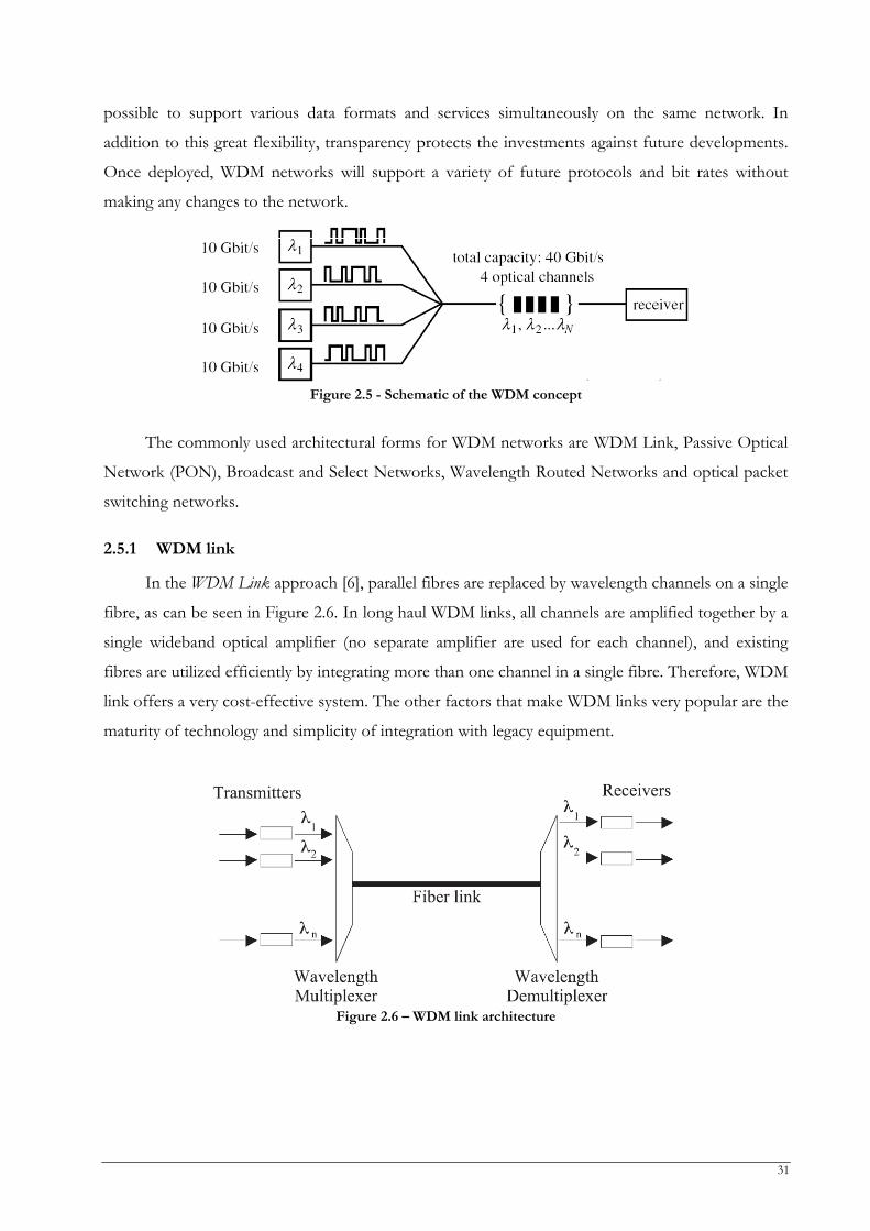
Figure 2.5 - Schematic of the WDM concept
The commonly used architectural forms for WDM networks are WDM Link, Passive Optical
Network (PON), Broadcast and Select Networks, Wavelength Routed Networks and optical packet
switching networks.
2.5.1 WDM link
In the WDM Link approach [6], parallel fibres are replaced by wavelength channels on a single
fibre, as can be seen in Figure 2.6. In long haul WDM links, all channels are amplified together by a
single wideband optical amplifier (no separate amplifier are used for each channel), and existing
fibres are utilized efficiently by integrating more than one channel in a single fibre. Therefore, WDM
link offers a very cost-effective system. The other factors that make WDM links very popular are the
maturity of technology and simplicity of integration with legacy equipment.
Figure 2.6 – WDM link architecture
32
2.5.2 Passive optical networks
The main features of the Passive optical network (PON) [7] are the sharing of fibre between the
head-end and the remote node, producing a tree or multiple star structure in the last mile, and the
centralized control of the network at the central office or optical line termination (OLT). Both
upstream traffic from the network nodes (known as optical network units, ONUs) and downstream
traffic from the core network (or traffic from one network node destined for another) are routed
through the OLT, the resources of which are shared between the ONUs. The single-wavelength
PON is well established for use in the access network, and upgrading to multiwavelength systems is
a natural progression. There are two broad approaches to implementing WDM over passive optical
networks. The first involves the use of tuneable receivers and tuneable transmitters at the customer
end, thus allowing reconfiguration of the network according to demand; the second uses fixed
transmitters and receivers, giving a set wavelength to a group of ONUs[8].
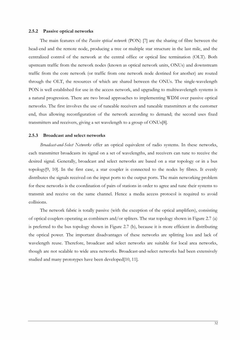
2.5.3 Broadcast and select networks
Broadcast-and-Select Networks offer an optical equivalent of radio systems. In these networks,
each transmitter broadcasts its signal on a set of wavelengths, and receivers can tune to receive the
desired signal. Generally, broadcast and select networks are based on a star topology or in a bus
topology[9, 10]. In the first case, a star coupler is connected to the nodes by fibres. It evenly
distributes the signals received on the input ports to the output ports. The main networking problem
for these networks is the coordination of pairs of stations in order to agree and tune their systems to
transmit and receive on the same channel. Hence a media access protocol is required to avoid
collisions.
The network fabric is totally passive (with the exception of the optical amplifiers), consisting
of optical couplers operating as combiners and/or spliters. The star topology shown in Figure 2.7 (a)
is preferred to the bus topology shown in Figure 2.7 (b), because it is more efficient in distributing
the optical power. The important disadvantages of these networks are splitting loss and lack of
wavelength reuse. Therefore, broadcast and select networks are suitable for local area networks,
though are not scalable to wide area networks. Broadcast-and-select networks had been extensively
studied and many prototypes have been developed[10, 11].
33
Figure 2.7 – Broadcast-and-select WDM networks: (a) star topology; (b) bus topology.
In single-hop systems [12] data is converted to electric from only at the end of the path, i.e.,
information once transmitted as light reaches its final destination directly without being converted to
electronic form in between. For single-hop broadcast-and-select networks to operate as packet
networks fast tuneable receivers and/or transmitters are required. Actually, the first optical packet
networks implemented were single-hop broadcast and select networks. Each station transmits on a
unique wavelength different from the others. All transmissions are broadcast to all stations and, at
each station, a tuneable optical filter selects one of the wavelengths for reception.
Multihop systems [13] are those where ever node has only a few fixed transmitters and
receivers. The multihop approach of the broadcast-and-select networks avoids tuning altogether.
Therefore a signal cannot always be directly transmitted from the source node to the destination
node. Instead signals have to be received at some intermediate nodes along the way, converted to
electronic and then retransmitted. Thus, over the physical broadcast topology, there is a logical
topology that determines the actual connectivity between the stations in the network.
2.5.4 Wavelength routed networks
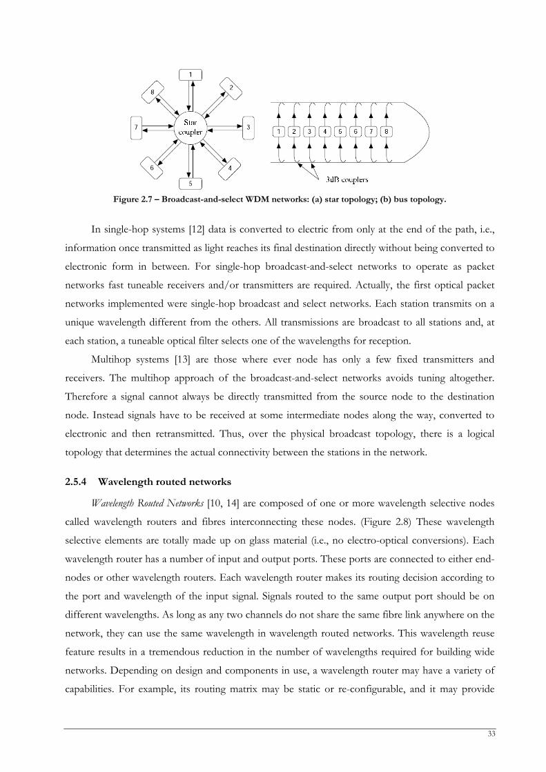
Wavelength Routed Networks [10, 14] are composed of one or more wavelength selective nodes
called wavelength routers and fibres interconnecting these nodes. (Figure 2.8) These wavelength
selective elements are totally made up on glass material (i.e., no electro-optical conversions). Each
wavelength router has a number of input and output ports. These ports are connected to either end-
nodes or other wavelength routers. Each wavelength router makes its routing decision according to
the port and wavelength of the input signal. Signals routed to the same output port should be on
different wavelengths. As long as any two channels do not share the same fibre link anywhere on the
network, they can use the same wavelength in wavelength routed networks. This wavelength reuse
feature results in a tremendous reduction in the number of wavelengths required for building wide
networks. Depending on design and components in use, a wavelength router may have a variety of
capabilities. For example, its routing matrix may be static or re-configurable, and it may provide
34
wavelength conversion or not. These features have a direct influence on the operation and scalability
of the network. Therefore, wavelength routed networks are the primary choice for optical backbone
networks[11].
b
a c
de
2
1 3
5 4
λ1
λ1
λ1
Lightpath
Fibre
Routing Node
End StationNode
Figure 2.8 – Wavelength routing network
2.5.5 Photonic packet switching networks
Photonic packet switching networks offers high-speed, data rate/format transparency, and
configurability, which are some of the important characteristics needed in future networks
supporting different forms of data[11, 15, 16]. The signals are converted to the electrical domain
before switching and processing. This means that the major advantages of optical packet switching,
i.e., speed and efficiency are lost due to the increased delay. The development is fast, and many
demonstrations of optical packet switches and networks have already been conducted in
laboratories. The biggest problem at the moment is the lack of optical RAM needed for buffering
the packets. Optical buffers are realized by using a length of fibre and are just simply delay lines, not
fully functional memories. Additionally, very high switching rates needed in packet networks cause
problems. Real packet switches include high amount of intelligent real-time software and hardware
dedicated to the control of the network as also quality of service guaranties, functions that are very
difficult to implement just in the optical domain. Another factor is the relatively primitive state of
the fast optical switching technology, compared to electronics. For these reasons packet switching
networks are still in infancy. So, in the near future, the development seems to lead to integration of
optical and electronic networks and the use of optical burst switching. [11]
35
2.6 Summary
Third generation networks appear due to the emergency of new optical technologies, concepts
and architectures. WDM was presented as the favourite choice to support the optical technology
that enables the realization of such networks. The most commonly used architectural forms for
WDM networks were presented. Wavelength routed networks and packet switching networks were
also discussed.

3 Optical Switching – State of the art
3.1 Introduction
Optical switches are key components in optical networks. In such networks they are used for a
enormous variety of applications such as provisioning of lightpaths, protection switching and as the
elements that allow high speed packet switched networks. Lots of different technologies are
available to realize optical switches. In this chapter, the most important types of switch architectures
and technologies are presented in section 3.3, and a comparison between its strengths, weaknesses
and potential applications is performed in section 3.4.
3.2 All optical switching approaches
Switching is an important and essential functionality in telecommunications, which can be
understood at two levels: a higher level that requires sophisticated electronics and the physical level
comprised by components and devices that “switch” signals within the network. Only components
at the physical level can be “all-optical”, and this chapter focuses on various types of all-optical
switching components that are available or in development for switching functions.
In practice, many optical switches actually are optoelectronic, with input optical signals
converted to electronic form for switching, and the switched electronic signals then driving an
optical transmitter. All-optical switches manipulate signals in the form of light, either by redirecting
all signals in a fibre or by selecting signals at certain wavelengths in wavelength-division multiplexed
systems. Some switches can isolate individual wavelengths, but typically their input is an individual
optical channel that was previously separated from other channels by a demultiplexing system. That
means they operate at the optical-channel level, without regard to what data stream the optical
channel is carrying. Electronic or optoelectronic switches are still required to manipulate the data
stream transmitted on each optical channel, such as breaking up a time-division multiplexed signal
into its component pieces for distribution at the end of a long-distance transmission line.
One further distinction is between “transparent” and “opaque” optical switches. [17] The
most current are transparent all-optical switches, because they transmit the original input light, without
converting it into some other form, as if you could “look” right through it. One simple example is a
moving-mirror switch, which reflects the input photons in different directions. Opaque optical switches
convert the input photons into some other form, and thus do not transmit them exactly as they were
38
received. They include optoelectronic types and others that convert the signal to a different
wavelength using optical or electronic techniques.
3.3 Optical switch fabrics
Most solutions for all-optical switching applications are mostly currently under study. Given
the wide range of applications for these devices, it seems reasonable that that we will not have a
single winning solution. First of all we must consider, in brief, the parameters taken in account when
we evaluate an optical switch.
Switching time – The most important parameter of a switch. It must be taken in account that
different applications have different switching time requirements.
Insertion Loss – The fraction of a signal power introduced by the switch. It is measured in dB
and must be as small as possible. The insertion loss of a switch should be about the same for all
input/output connections, this is referred to as loss uniformity.
Crosstalk – The ratio of power at a specific output from the desired input, to the power from
all other inputs
Extinction Ratio – The ratio of the output power in the on-state to the output power in the off-
state. This ratio should be as large as possible.
Polarization dependence loss (PDL) – Measured loss of the switch due to the different losses
observed in the two states of polarization. It is desirable that optical switches have low PDL.
Reliability – The ability to perform the desired switching operation after ‘a million’ of cycles.
The reliability is also a measure of the switching capability after the switch remaining untouched for
a long period of time.
Energy usage – Power consumption of the switching device.
Scalability – The ability to build switches with large port counts that perform adequately.
Temperature resistance – The switch ability to maintain the desired behaviour facing temperature
changes.
The main optical switching technologies [17-20] available today follow:
3.3.1 Optomechanical Switches
Optomechanical technology was the first commercially available technology for optical
switching. The switching operation is performed by some mechanical means, such as prisms,
mirrors and directional couplers. The electromechanical actuators are employed to redirect a light
beam. One type of optomechanical switch inserts and retracts a reflective surface into a light stream
to redirect it to another port. Another architecture redirects the light stream by bending a grating-
written fibre. In terms of optical insertion loss and switching speed, performance characteristics of
39
optomechanical switches vary according to architecture; performance can range from low to high
loss and slow to fast speed. However, the fundamental drawback for optomechanical switches is the
durability and cycle limitation of the mechanical actuators.
3.3.2 Micro-Optical-Mechanical-Systems Switches
Micro-Electro-Mechanical System devices (MEMS) can be considered as a subcategory of
optomechanical switches, however, because of the fabrication processes and miniature nature of the
devices, they have different characteristics, performance and reliability concerns.
Microelectromechanical systems (MEMS) have attracted wide attention for optical switching
because of their versatility. Originally developed for display applications, MEMS are assemblies of
tiny mechanical components fabricated by depositing layers on a substrate, then etching away
selected material using standard photolithographic technology. A variety of MEMS devices have
been developed for optical switching that share common features. Typically movable components
are suspended on flexible structures above a base layer. Either electrostatic or magnetic forces
between the base and the elevated components move the structures. Electrostatic forces that create
different charges are easier to control and are more widely used, but magnetic forces are stronger.
However, magnetic forces—typically between an electromagnet on the surface and a magnet on the
movable structure—require shielding from external fields. Photolithography can fabricate many
components on the surface, producing an array of identical switching components.
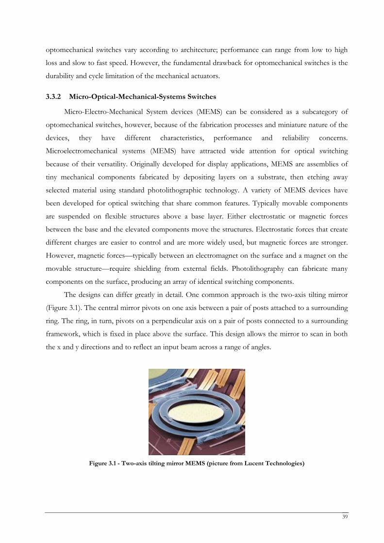
The designs can differ greatly in detail. One common approach is the two-axis tilting mirror
(Figure 3.1). The central mirror pivots on one axis between a pair of posts attached to a surrounding
ring. The ring, in turn, pivots on a perpendicular axis on a pair of posts connected to a surrounding
framework, which is fixed in place above the surface. This design allows the mirror to scan in both
the x and y directions and to reflect an input beam across a range of angles.
Figure 3.1 - Two-axis tilting mirror MEMS (picture from Lucent Technologies)
40
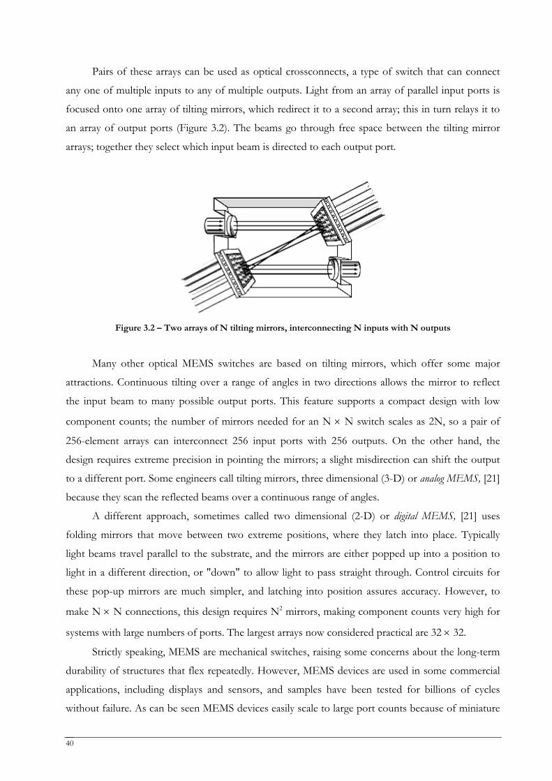
Pairs of these arrays can be used as optical crossconnects, a type of switch that can connect
any one of multiple inputs to any of multiple outputs. Light from an array of parallel input ports is
focused onto one array of tilting mirrors, which redirect it to a second array; this in turn relays it to
an array of output ports (Figure 3.2). The beams go through free space between the tilting mirror
arrays; together they select which input beam is directed to each output port.
Figure 3.2 – Two arrays of N tilting mirrors, interconnecting N inputs with N outputs
Many other optical MEMS switches are based on tilting mirrors, which offer some major
attractions. Continuous tilting over a range of angles in two directions allows the mirror to reflect
the input beam to many possible output ports. This feature supports a compact design with low
component counts; the number of mirrors needed for an N × N switch scales as 2N, so a pair of
256-element arrays can interconnect 256 input ports with 256 outputs. On the other hand, the
design requires extreme precision in pointing the mirrors; a slight misdirection can shift the output
to a different port. Some engineers call tilting mirrors, three dimensional (3-D) or analog MEMS, [21]
because they scan the reflected beams over a continuous range of angles.
A different approach, sometimes called two dimensional (2-D) or digital MEMS, [21] uses
folding mirrors that move between two extreme positions, where they latch into place. Typically
light beams travel parallel to the substrate, and the mirrors are either popped up into a position to
light in a different direction, or "down" to allow light to pass straight through. Control circuits for
these pop-up mirrors are much simpler, and latching into position assures accuracy. However, to
make N × N connections, this design requires N2 mirrors, making component counts very high for
systems with large numbers of ports. The largest arrays now considered practical are 32 × 32.
Strictly speaking, MEMS are mechanical switches, raising some concerns about the long-term
durability of structures that flex repeatedly. However, MEMS devices are used in some commercial
applications, including displays and sensors, and samples have been tested for billions of cycles
without failure. As can be seen MEMS devices easily scale to large port counts because of miniature
41
sizes and semiconductor fabrication processes, but due to the density and microscopic size of the
light paths entering and exiting the substrate, MEMS can be a challenge to package.
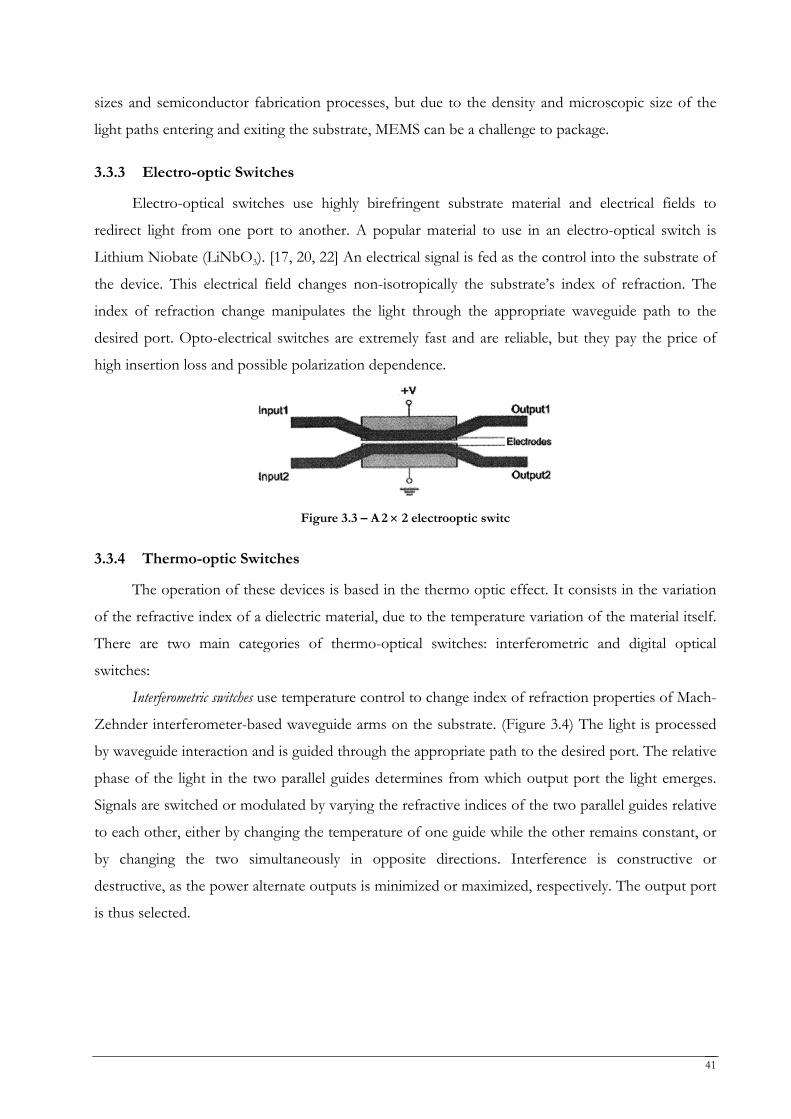
3.3.3 Electro-optic Switches
Electro-optical switches use highly birefringent substrate material and electrical fields to
redirect light from one port to another. A popular material to use in an electro-optical switch is
Lithium Niobate (LiNbO3). [17, 20, 22] An electrical signal is fed as the control into the substrate of
the device. This electrical field changes non-isotropically the substrate’s index of refraction. The
index of refraction change manipulates the light through the appropriate waveguide path to the
desired port. Opto-electrical switches are extremely fast and are reliable, but they pay the price of
high insertion loss and possible polarization dependence.
Figure 3.3 – A 2 × 2 electrooptic switc
3.3.4 Thermo-optic Switches
The operation of these devices is based in the thermo optic effect. It consists in the variation
of the refractive index of a dielectric material, due to the temperature variation of the material itself.
There are two main categories of thermo-optical switches: interferometric and digital optical
switches:
Interferometric switches use temperature control to change index of refraction properties of Mach-
Zehnder interferometer-based waveguide arms on the substrate. (Figure 3.4) The light is processed
by waveguide interaction and is guided through the appropriate path to the desired port. The relative
phase of the light in the two parallel guides determines from which output port the light emerges.
Signals are switched or modulated by varying the refractive indices of the two parallel guides relative
to each other, either by changing the temperature of one guide while the other remains constant, or
by changing the two simultaneously in opposite directions. Interference is constructive or
destructive, as the power alternate outputs is minimized or maximized, respectively. The output port
is thus selected.
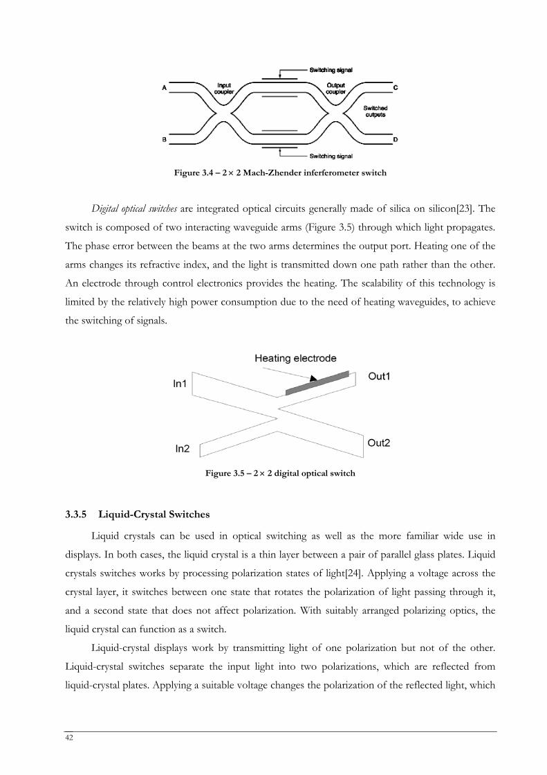
42
Figure 3.4 – 2 × 2 Mach-Zhender inferferometer switch
Digital optical switches are integrated optical circuits generally made of silica on silicon[23]. The
switch is composed of two interacting waveguide arms (Figure 3.5) through which light propagates.
The phase error between the beams at the two arms determines the output port. Heating one of the
arms changes its refractive index, and the light is transmitted down one path rather than the other.
An electrode through control electronics provides the heating. The scalability of this technology is
limited by the relatively high power consumption due to the need of heating waveguides, to achieve
the switching of signals.
Figure 3.5 – 2 × 2 digital optical switch
3.3.5 Liquid-Crystal Switches
Liquid crystals can be used in optical switching as well as the more familiar wide use in
displays. In both cases, the liquid crystal is a thin layer between a pair of parallel glass plates. Liquid
crystals switches works by processing polarization states of light[24]. Applying a voltage across the
crystal layer, it switches between one state that rotates the polarization of light passing through it,
and a second state that does not affect polarization. With suitably arranged polarizing optics, the
liquid crystal can function as a switch.
Liquid-crystal displays work by transmitting light of one polarization but not of the other.
Liquid-crystal switches separate the input light into two polarizations, which are reflected from
liquid-crystal plates. Applying a suitable voltage changes the polarization of the reflected light, which
43
the polarizing optics deflects differently than if its polarization is not rotated, switching it between
output ports.
2
1
2
1
Figure 3.6 – Principle of operation of a 1 × 2 liquid-crystal optical switch
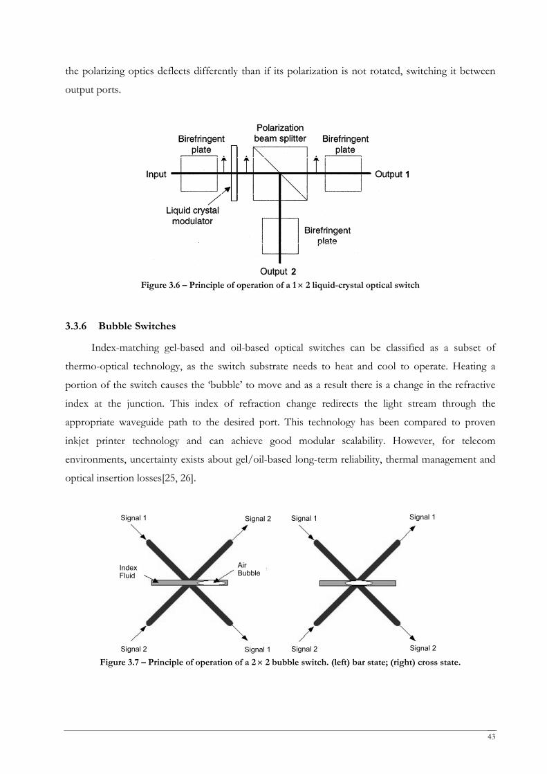
3.3.6 Bubble Switches
Index-matching gel-based and oil-based optical switches can be classified as a subset of
thermo-optical technology, as the switch substrate needs to heat and cool to operate. Heating a
portion of the switch causes the ‘bubble’ to move and as a result there is a change in the refractive
index at the junction. This index of refraction change redirects the light stream through the
appropriate waveguide path to the desired port. This technology has been compared to proven
inkjet printer technology and can achieve good modular scalability. However, for telecom
environments, uncertainty exists about gel/oil-based long-term reliability, thermal management and
optical insertion losses[25, 26].
Signal 1
Signal 2
Signal 2
Signal 1
Signal 1
Signal 2
Signal 1
Signal 2
AirBubble
IndexFluid
Signal 1
Signal 2
Signal 2
Signal 1
Signal 1
Signal 2
Signal 1
Signal 2
AirBubble
IndexFluid
Figure 3.7 – Principle of operation of a 2 × 2 bubble switch. (left) bar state; (right) cross state.
44
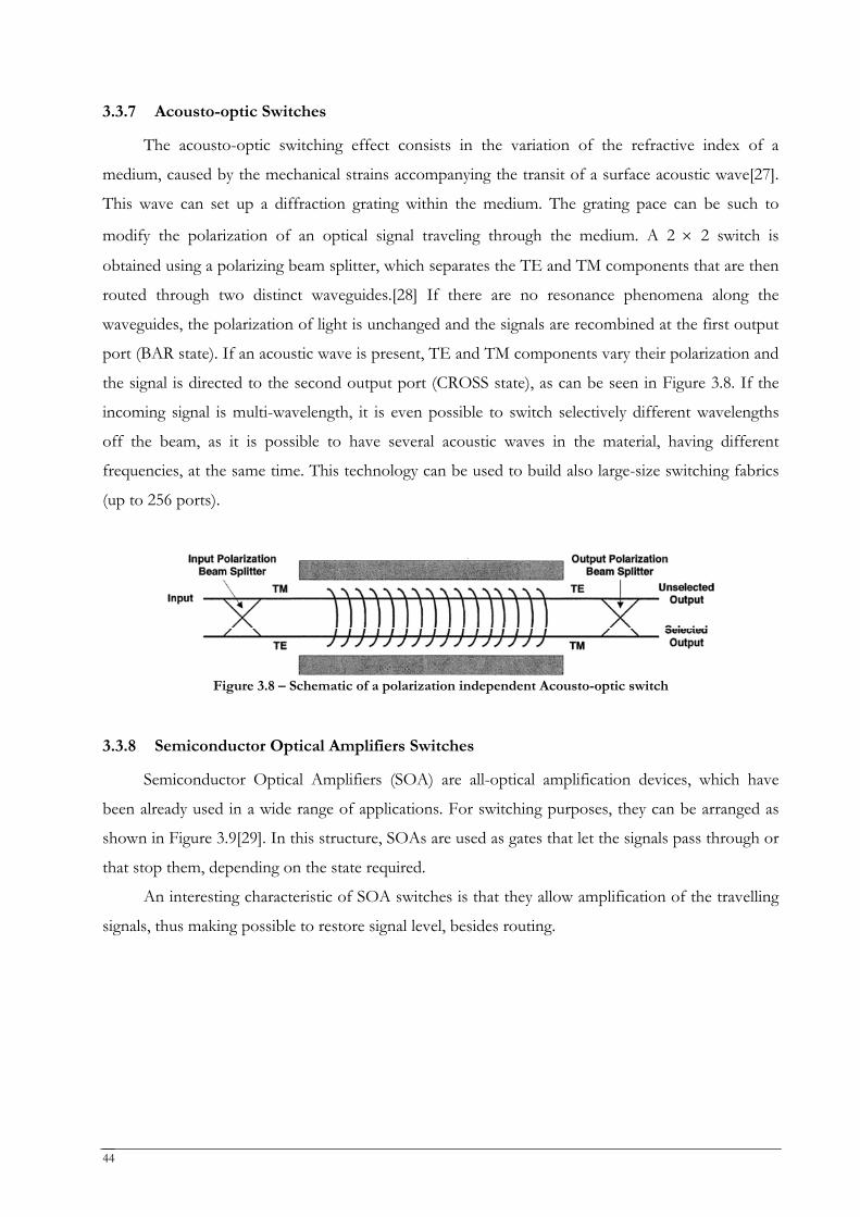
3.3.7 Acousto-optic Switches
The acousto-optic switching effect consists in the variation of the refractive index of a
medium, caused by the mechanical strains accompanying the transit of a surface acoustic wave[27].
This wave can set up a diffraction grating within the medium. The grating pace can be such to
modify the polarization of an optical signal traveling through the medium. A 2 × 2 switch is
obtained using a polarizing beam splitter, which separates the TE and TM components that are then
routed through two distinct waveguides.[28] If there are no resonance phenomena along the
waveguides, the polarization of light is unchanged and the signals are recombined at the first output
port (BAR state). If an acoustic wave is present, TE and TM components vary their polarization and
the signal is directed to the second output port (CROSS state), as can be seen in Figure 3.8. If the
incoming signal is multi-wavelength, it is even possible to switch selectively different wavelengths
off the beam, as it is possible to have several acoustic waves in the material, having different
frequencies, at the same time. This technology can be used to build also large-size switching fabrics
(up to 256 ports).
Figure 3.8 – Schematic of a polarization independent Acousto-optic switch
3.3.8 Semiconductor Optical Amplifiers Switches
Semiconductor Optical Amplifiers (SOA) are all-optical amplification devices, which have
been already used in a wide range of applications. For switching purposes, they can be arranged as
shown in Figure 3.9[29]. In this structure, SOAs are used as gates that let the signals pass through or
that stop them, depending on the state required.
An interesting characteristic of SOA switches is that they allow amplification of the travelling
signals, thus making possible to restore signal level, besides routing.
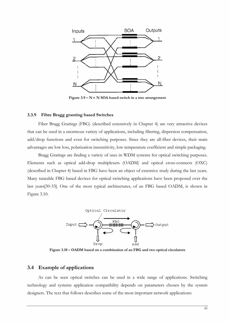
45
Figure 3.9 – N × N SOA based switch in a tree arrangement
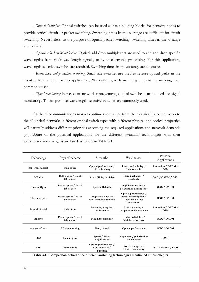
3.3.9 Fibre Bragg granting based Switches
Fiber Bragg Gratings (FBG) (described extensively in Chapter 4) are very attractive devices
that can be used in a enormous variety of applications, including filtering, dispersion compensation,
add/drop functions and even for switching purposes. Since they are all-fiber devices, their main
advantages are low loss, polarization insensitivity, low temperature coefficient and simple packaging.
Bragg Gratings are finding a variety of uses in WDM systems for optical switching purposes.
Elements such as optical add-drop multiplexers (OADM) and optical cross-connects (OXC)
(described in Chapter 4) based in FBG have been an object of extensive study during the last years.
Many tuneable FBG based devices for optical switching applications have been proposed over the
last years[30-33]. One of the most typical architectures, of an FBG based OADM, is shown in
Figure 3.10.
Figure 3.10 – OADM based on a combination of an FBG and two optical circulators
3.4 Example of applications
As can be seen optical switches can be used in a wide range of applications. Switching
technology and systems application compatibility depends on parameters chosen by the system
designers. The text that follows describes some of the most important network applications:
46
- Optical Switching: Optical switches can be used as basic building blocks for network nodes to
provide optical circuit or packet switching. Switching times in the ms range are sufficient for circuit
switching. Nevertheless, to the purpose of optical packet switching, switching times in the ns range
are required.
- Optical add-drop Muliplexing: Optical add-drop multiplexers are used to add and drop specific
wavelengths from multi-wavelength signals, to avoid electronic processing. For this application,
wavelength selective switches are required. Switching times in the ms range are adequate.
- Restoration and protection switching: Small-size switches are used to restore optical paths in the
event of link failure. For this application, 2×2 switches, with switching times in the ms range, are
commonly used.
- Signal monitoring: For ease of network management, optical switches can be used for signal
monitoring. To this purpose, wavelength-selective switches are commonly used.
As the telecommunications market continues to mature from the electrical based networks to
the all optical networks, different optical switch types with different physical and optical properties
will naturally address different priorities according the required applications and network demands
[34]. Some of the potential applications for the different switching technologies with their
weaknesses and strengths are listed as follow in Table 3.1.
Technology Physical scheme Strengths Weaknesses Potential Applications
Optomechanical bulk optics Optical performance /
old technology Low speed / Bulky /
Low scalable Protection / OADM /
OSM
MEMS Bulk optics / Batch
fabrication Size / Highly Scalable
Hard packaging / reliability
OXC / OADM / OSM
Electro-Optic Planar optics / Batch
fabrication Speed / Reliable
high insertion loss / polarization dependence
OXC / OADM
Thermo-Optic Planar optics / Batch
fabrication Integration / Wafer-
level manufacturability
Optical performance / power consumption /
low speed / low scalability
OXC / OADM
Liquid-Crystal Bulk optics Reliability / Optical
performance Low scalability /
temperature dependence Protection / OADM /
OSM
Bubble Planar optics / Batch
fabrication Modular scalability
Unclear reliability / high insertion loss
OXC / OADM
Acousto-Optic RF signal tuning Size / Speed Optical performance OXC / OADM
SOA Planar optics Speed / Allow amplification
Expensive / polarization dependence
OXC
FBG Fibre optics Optical performance /
Low crosstalk / Tuneable
Size / Low speed / Limited scalability
OXC/ OADM / OSM
Table 3.1 – Comparison between the different switching technologies mentioned in this chapter
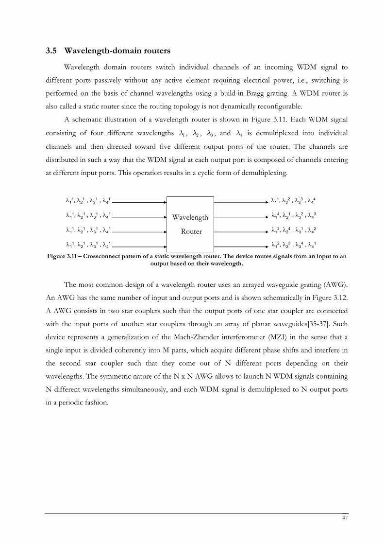
47
3.5 Wavelength-domain routers
Wavelength domain routers switch individual channels of an incoming WDM signal to
different ports passively without any active element requiring electrical power, i.e., switching is
performed on the basis of channel wavelengths using a build-in Bragg grating. A WDM router is
also called a static router since the routing topology is not dynamically reconfigurable.
A schematic illustration of a wavelength router is shown in Figure 3.11. Each WDM signal
consisting of four different wavelengths 1λ , 2λ , 3λ , and 4λ is demultiplexed into individual
channels and then directed toward five different output ports of the router. The channels are
distributed in such a way that the WDM signal at each output port is composed of channels entering
at different input ports. This operation results in a cyclic form of demultiplexing.
Wavelength
Router
λ11, λ2
1 , λ31 , λ4
1
λ11, λ2
1 , λ31 , λ4
1
λ11, λ2
1 , λ31 , λ4
1
λ11, λ2
1 , λ31 , λ4
1
λ11, λ2
2 , λ33 , λ4
4
λ14, λ2
1 , λ32 , λ4
3
λ13, λ2
4 , λ31 , λ4
2
λ12, λ2
3 , λ34 , λ4
1
Figure 3.11 – Crossconnect pattern of a static wavelength router. The device routes signals from an input to an
output based on their wavelength.
The most common design of a wavelength router uses an arrayed waveguide grating (AWG).
An AWG has the same number of input and output ports and is shown schematically in Figure 3.12.
A AWG consists in two star couplers such that the output ports of one star coupler are connected
with the input ports of another star couplers through an array of planar waveguides[35-37]. Such
device represents a generalization of the Mach-Zhender interferometer (MZI) in the sense that a
single input is divided coherently into M parts, which acquire different phase shifts and interfere in
the second star coupler such that they come out of N different ports depending on their
wavelengths. The symmetric nature of the N x N AWG allows to launch N WDM signals containing
N different wavelengths simultaneously, and each WDM signal is demultiplexed to N output ports
in a periodic fashion.
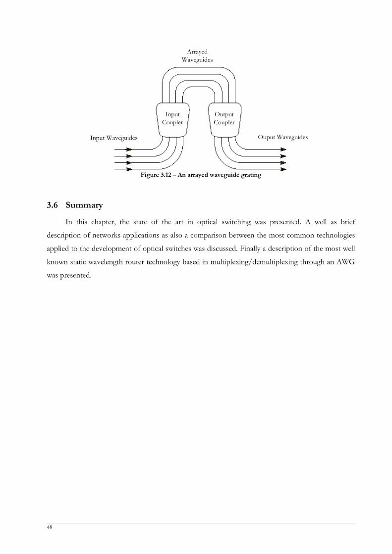
48
Input Waveguides Ouput Waveguides
Input Coupler
Output Coupler
Arrayed Waveguides
Figure 3.12 – An arrayed waveguide grating
3.6 Summary
In this chapter, the state of the art in optical switching was presented. A well as brief
description of networks applications as also a comparison between the most common technologies
applied to the development of optical switches was discussed. Finally a description of the most well
known static wavelength router technology based in multiplexing/demultiplexing through an AWG
was presented.
4 Fibre Bragg Gratings Technology
4.1 Introduction
Silica fibres can change their optical properties permanently when exposed to a intense
radiation beam from a laser operating in the blue or ultraviolet optical spectral region. The observed
photosensitive effect, explained in section 4.3, can be used to induce periodic changes in the
effective index along a specific fibre length, that results in the formation of an intracore structure
called Fibre Bragg Grating. Fibre Bragg gratings can be designed to operate over a wide range of
wavelengths, although our particular interest reside in the wavelength region near of the 1500 nm
because of its high relevance in the modern fibre optic communication systems.
The Bragg grating diffraction phenomenon, the physical mechanism responsible by the
photosentivity, will be discussed in section 4.2. The various techniques used to make fibre gratings,
the spectral characteristics of those narrowband optical filters are described in section 4.4, and the
used of this concept in moderns optical switching systems will be presented in section 4.6.
4.2 Bragg diffraction
The diffraction theory of the gratings show that when an amount of light is incident at an
angle iθ (measured with respect to the planes of constant refractive index) it is diffracted at an angle
rθ such that
sin sin mri n
λθ θ− =Λ
(4.1)
where Λ is the gating period, /nλ is the wavelength of light inside the medium that has an average
refractive index n , and m is the order of the Bragg diffraction.
A Bragg grating acts as a reflector for a specific wavelength of light for which the phase
matching condition is satisfied. If 1m = , and for /2i rθ θ π= = , the period of the grating Λ , is
related to the vacuum wavelength λ as
2nλ = Λ (4.2)
50
This condition is well known as the Bragg condition, and fibre gratings that satisfies it, are referred to
as fibre Bragg gratings (FBG). Physically, the Bragg condition ensures that the week reflections
occurring throughout the grating add up in phase to produce a strong reflection. For a fibre Bragg
grating reflecting light in the region of 1500 nm, the grating period Λ≈0.5 μm.
Bragg gratings inside optical fibres were first formed in 1978 by irradiating a silica fibre for a
few minutes with a intense argon-ion laser beam [38]. The grating period was fixed by the argon-ion
laser wavelength, and the grating reflected light only within a narrow region around that wavelength.
The mechanism behind the grating formation can be understood as follows. The 4% reflection
occurring at the two fibre air interfaces create a standing-wave pattern such that the laser light is
absorbed only in the bright regions. If the glass structures changes in such a way that the refractive
index increases permanently in the bright regions, an index grating is formed. Curiously it was only
from 1989 on, that fibre Bragg gratings became a topic of intense investigation, mostly due to the
fact of the observation of second-harmonic generation in photosensitive fibres. In that year, a paper
presented a side-exposed holographic technique that was used to make FBG with controllable
period [39]. This technique was quickly adopted to produce fibre gratings in the third
telecommunication window, near 1500 nm [40]. During the early 90s considerable work was done in
order to understand the physical mechanism behind photosensitivity of fibres and to develop
techniques that make capable large changes in the fibre refractive index [41, 42]. By 1995, FBGs
became available commercially, and by 1997 they appeared as standard components in lightwave
communication systems.
4.3 Photosensitivity
Photosensitivity in optical fibres can be defined as the maximum refraction index change that
can be induced in an optical fibre through exposure to UV (ultra-violet) light [43]. A well known
characteristic of optical fibres is the high absorption verified for wavelengths in the UV band (<300
nm). In fact, at these wavelengths the photon energy is considerable and electronic links resonance
is seen. UV exposure is a single photon process and as such, the induced index alteration is
~6 orders of magnitude higher than the one verified in exposure with visible light. Fibres with high
germanium doping proved to be highly photosensitive. Theoretical models (still not proven) that
explain this phenomenon state that the defects introduced by the germanium in the crystalline
structure of the fibre are responsible for the achieved photosensitivity. Recently, new techniques
were developed that increase the photosensitivity of any type of fibre. This is important because a
standard fibre with germanium doping does not have a sufficient doping profile as to obtain enough
photosensitivity to inscribe the diffraction pattern correctly. Among these techniques we have
51
hydrogenation or hydrogen loading, flame brushing, and boron co-doping. The first technique
(hydrogenation) is the most widely implemented. Hydrogen molecules are diffused into the fibre
core and penetrate the crystalline structure at high pressure and temperatures. The presence of these
molecules makes the fibre much more sensitive to refractive index changes due to the exposure to
UV light. It should be noted that the increased fibre/waveguide photosensitivity as a result of
hydrogen loading is not a permanent effect, and as the hydrogen diffuses out, the photosensitivity
decreases.
The other processes are also valid as means of increasing the photosensitivity of optical fibres
and have their advantages but hydrogenation is considered the best in terms of final results for
telecommunications applications. There are several advantages of enhancing fibre photosensitivity
though hydrogenation. The first and foremost is that it allows strong Bragg gratings to be fabricated
in any type of germanosilica fibre, including the standard telecommunications fibres that typically
have low germanium concentration, and hence, low intrinsic photosensitivity. Second, permanent
changes occur only in regions that are UV irradiated. Finally, unreacted hydrogen in other sections
of the fibre slowly diffuses out, thus leaving negligible absorption losses at the optical
communication windows.
The physical mechanisms through which fibres get their refractive index changed are not
completely explained yet. Three models have been reported in literature that describes this
phenomenon. Suitable references are provided to analyze this subject further [41, 44].
4.4 Fibre Bragg Gratings fabrication techniques
Inscribing diffraction patterns in a fibre is a complicated and high precision process. As
previously stated, inscription of these patterns requires a high power UV light source, centred at
244 nm, in the Germanium-Oxygen (GeO) defects or wrong bonds. Energy densities by unit area
used to efficiently write diffraction gratings have a threshold of ≈150 mJ/cm2. These values demand
the use of a UV laser source. Although there are several possibilities to obtain laser emission at
244 nm, like the Argon or Nd-YAG laser with doubled and quadrupled frequency, respectively,
generally the choice falls in the use of a KrF excimer laser. This laser’s wavelength is perfectly
centered in the 244 nm absorption peak, meaning that the writing of gratings can be performed
directly without the need for frequency multiplication crystals. This laser emits optical pulses with a
duration of 20 ns with an energy of 100 mJ to 1.4 J per impulse. The energy density over the
transversal section of the beam is 3×1 cm2 and it is non-uniform having a high divergence profile.
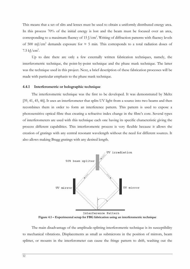
52
This means that a set of slits and lenses must be used to obtain a uniformly distributed energy area.
In this process 70% of the initial energy is lost and the beam must be focused over an area,
corresponding to a maximum fluency of 15 J/cm2. Writing of diffraction patterns with fluency levels
of 500 mJ/cm2 demands exposure for ≈ 5 min. This corresponds to a total radiation doses of
7.5 kJ/cm2.
Up to date there are only a few externally written fabrication techniques, namely, the
interferometric technique, the point-by-point technique and the phase mask technique. The latter
was the technique used in this project. Next, a brief description of these fabrication processes will be
made with particular emphasis to the phase mask technique.
4.4.1 Interferometric or holographic technique
The interferometric technique was the first to be developed. It was demonstrated by Meltz
[39, 41, 45, 46]. It uses an interferometer that splits UV light from a source into two beams and then
recombines them in order to form an interference pattern. This pattern is used to expose a
photosensitive optical fibre thus creating a refractive index change in the fibre’s core. Several types
of interferometers are used with this technique each one having its specific characteristic giving the
process different capabilities. This interferometric process is very flexible because it allows the
creation of gratings with any central resonant wavelength without the need for different sources. It
also allows making Bragg gratings with any desired length.
Figure 4.1 – Experimental setup for FBG fabrication using an interferometric technique
The main disadvantage of the amplitude-splitting interferometric technique is its susceptibility
to mechanical vibrations. Displacements as small as submicrons in the position of mirrors, beam
splitter, or mounts in the interferometer can cause the fringe pattern to drift, washing out the
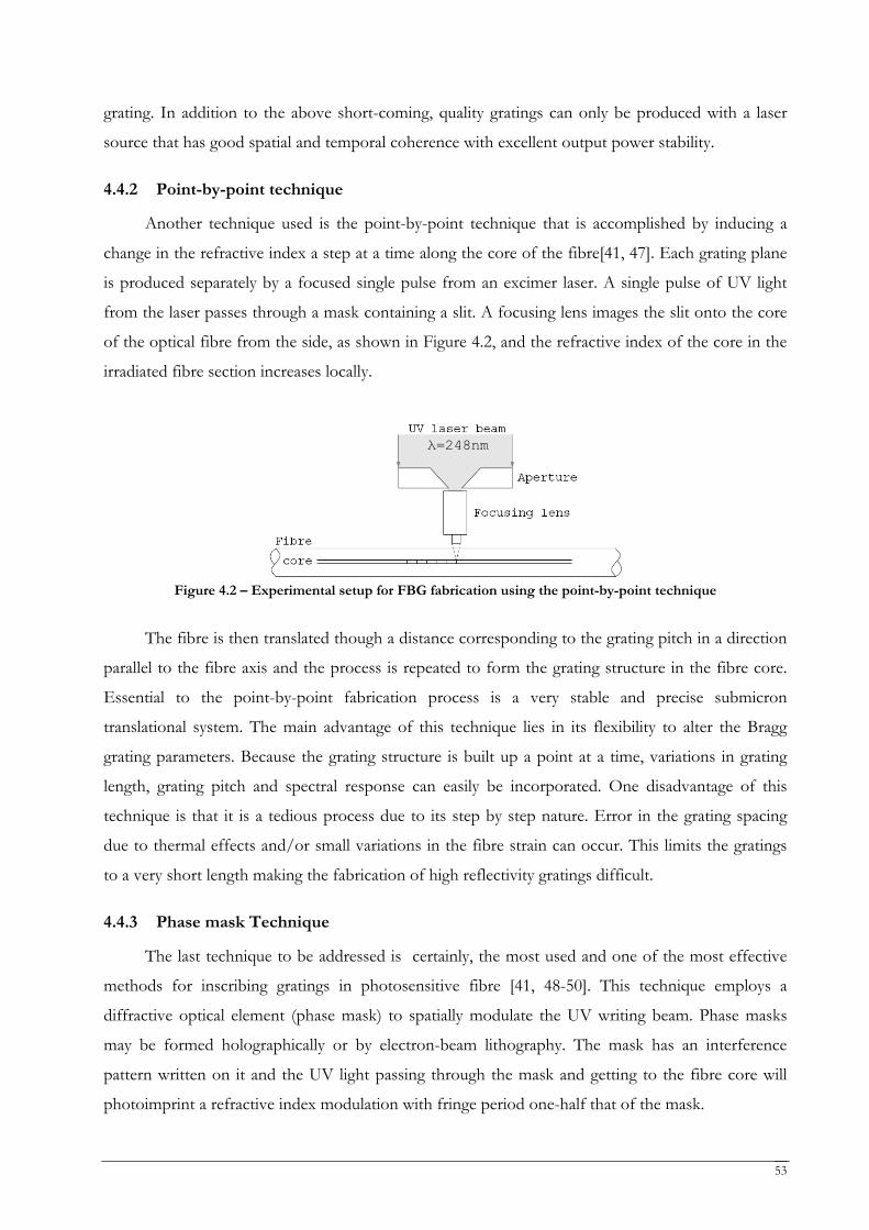
53
grating. In addition to the above short-coming, quality gratings can only be produced with a laser
source that has good spatial and temporal coherence with excellent output power stability.
4.4.2 Point-by-point technique
Another technique used is the point-by-point technique that is accomplished by inducing a
change in the refractive index a step at a time along the core of the fibre[41, 47]. Each grating plane
is produced separately by a focused single pulse from an excimer laser. A single pulse of UV light
from the laser passes through a mask containing a slit. A focusing lens images the slit onto the core
of the optical fibre from the side, as shown in Figure 4.2, and the refractive index of the core in the
irradiated fibre section increases locally.
Figure 4.2 – Experimental setup for FBG fabrication using the point-by-point technique
The fibre is then translated though a distance corresponding to the grating pitch in a direction
parallel to the fibre axis and the process is repeated to form the grating structure in the fibre core.
Essential to the point-by-point fabrication process is a very stable and precise submicron
translational system. The main advantage of this technique lies in its flexibility to alter the Bragg
grating parameters. Because the grating structure is built up a point at a time, variations in grating
length, grating pitch and spectral response can easily be incorporated. One disadvantage of this
technique is that it is a tedious process due to its step by step nature. Error in the grating spacing
due to thermal effects and/or small variations in the fibre strain can occur. This limits the gratings
to a very short length making the fabrication of high reflectivity gratings difficult.
4.4.3 Phase mask Technique
The last technique to be addressed is certainly, the most used and one of the most effective
methods for inscribing gratings in photosensitive fibre [41, 48-50]. This technique employs a
diffractive optical element (phase mask) to spatially modulate the UV writing beam. Phase masks
may be formed holographically or by electron-beam lithography. The mask has an interference
pattern written on it and the UV light passing through the mask and getting to the fibre core will
photoimprint a refractive index modulation with fringe period one-half that of the mask.
λ=248nm
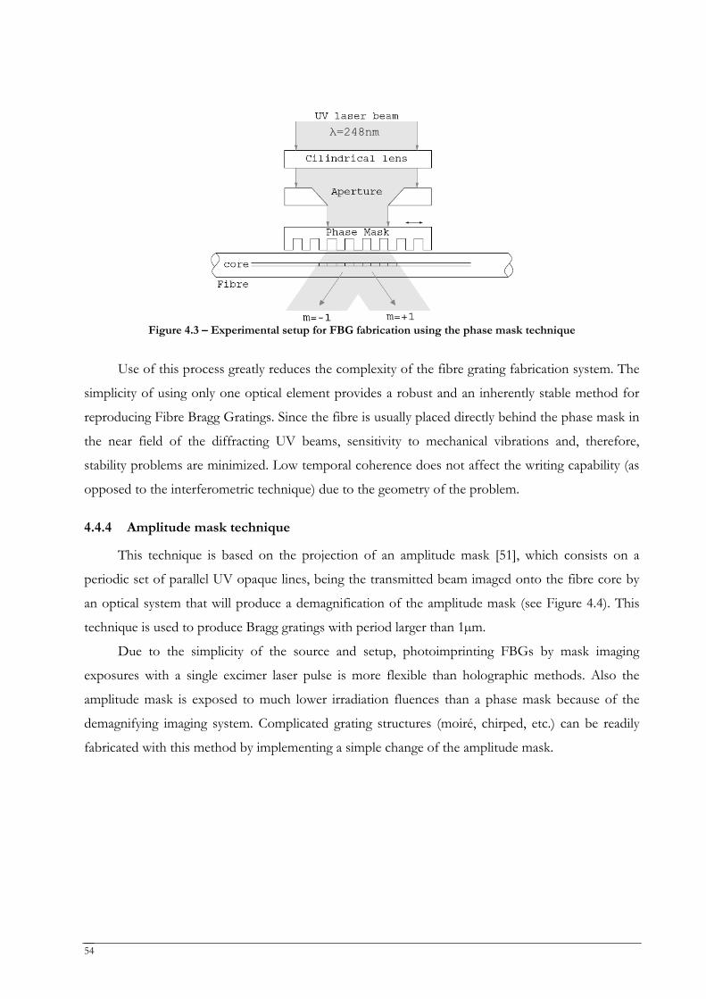
54
Figure 4.3 – Experimental setup for FBG fabrication using the phase mask technique
Use of this process greatly reduces the complexity of the fibre grating fabrication system. The
simplicity of using only one optical element provides a robust and an inherently stable method for
reproducing Fibre Bragg Gratings. Since the fibre is usually placed directly behind the phase mask in
the near field of the diffracting UV beams, sensitivity to mechanical vibrations and, therefore,
stability problems are minimized. Low temporal coherence does not affect the writing capability (as
opposed to the interferometric technique) due to the geometry of the problem.
4.4.4 Amplitude mask technique
This technique is based on the projection of an amplitude mask [51], which consists on a
periodic set of parallel UV opaque lines, being the transmitted beam imaged onto the fibre core by
an optical system that will produce a demagnification of the amplitude mask (see Figure 4.4). This
technique is used to produce Bragg gratings with period larger than 1µm.
Due to the simplicity of the source and setup, photoimprinting FBGs by mask imaging
exposures with a single excimer laser pulse is more flexible than holographic methods. Also the
amplitude mask is exposed to much lower irradiation fluences than a phase mask because of the
demagnifying imaging system. Complicated grating structures (moiré, chirped, etc.) can be readily
fabricated with this method by implementing a simple change of the amplitude mask.
λ=248nm
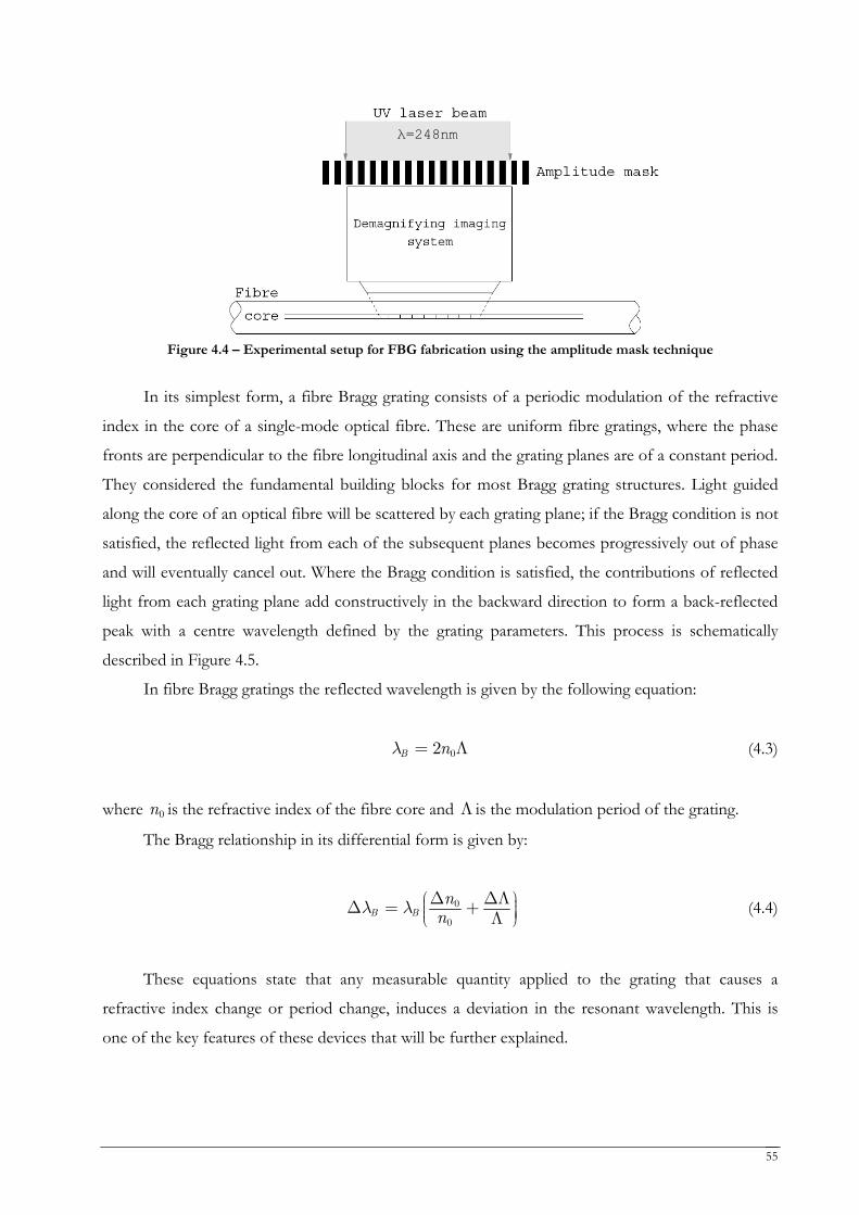
55
Figure 4.4 – Experimental setup for FBG fabrication using the amplitude mask technique
In its simplest form, a fibre Bragg grating consists of a periodic modulation of the refractive
index in the core of a single-mode optical fibre. These are uniform fibre gratings, where the phase
fronts are perpendicular to the fibre longitudinal axis and the grating planes are of a constant period.
They considered the fundamental building blocks for most Bragg grating structures. Light guided
along the core of an optical fibre will be scattered by each grating plane; if the Bragg condition is not
satisfied, the reflected light from each of the subsequent planes becomes progressively out of phase
and will eventually cancel out. Where the Bragg condition is satisfied, the contributions of reflected
light from each grating plane add constructively in the backward direction to form a back-reflected
peak with a centre wavelength defined by the grating parameters. This process is schematically
described in Figure 4.5.
In fibre Bragg gratings the reflected wavelength is given by the following equation:
02B nλ = Λ (4.3)
where 0n is the refractive index of the fibre core and Λ is the modulation period of the grating.
The Bragg relationship in its differential form is given by:
0
0B B
nnλ λ
⎛ ⎞⎟⎜ ⎟⎜ ⎟⎟⎜⎝ ⎠Δ ΔΛΔ = +
Λ (4.4)
These equations state that any measurable quantity applied to the grating that causes a
refractive index change or period change, induces a deviation in the resonant wavelength. This is
one of the key features of these devices that will be further explained.
λ=248nm
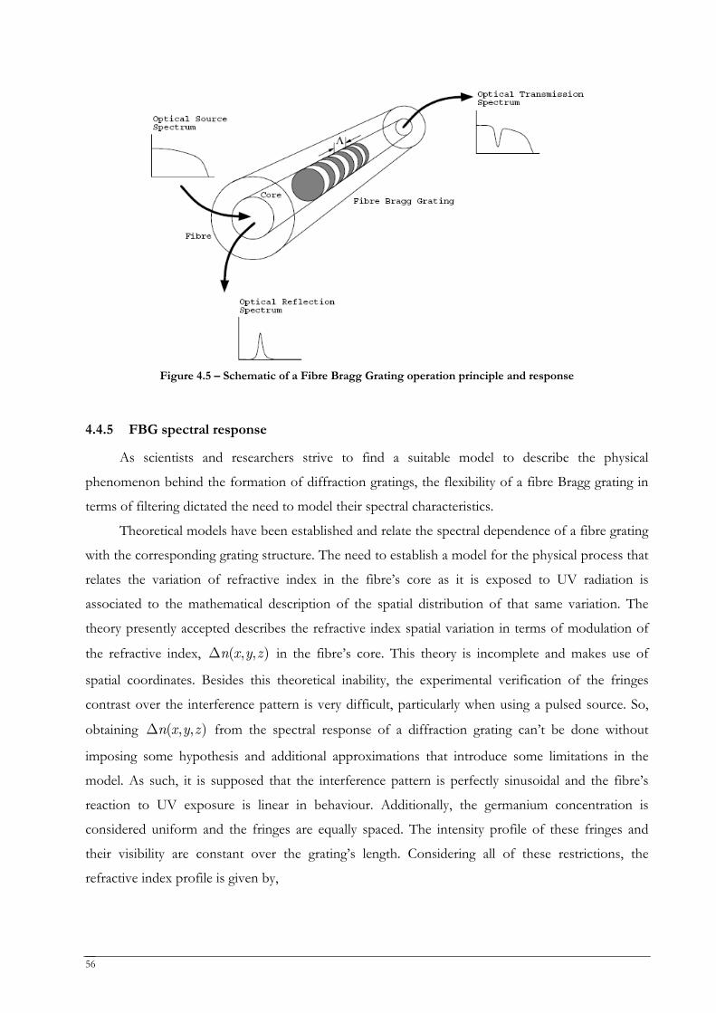
56
Figure 4.5 – Schematic of a Fibre Bragg Grating operation principle and response
4.4.5 FBG spectral response
As scientists and researchers strive to find a suitable model to describe the physical
phenomenon behind the formation of diffraction gratings, the flexibility of a fibre Bragg grating in
terms of filtering dictated the need to model their spectral characteristics.
Theoretical models have been established and relate the spectral dependence of a fibre grating
with the corresponding grating structure. The need to establish a model for the physical process that
relates the variation of refractive index in the fibre’s core as it is exposed to UV radiation is
associated to the mathematical description of the spatial distribution of that same variation. The
theory presently accepted describes the refractive index spatial variation in terms of modulation of
the refractive index, ( , , )n x y zΔ in the fibre’s core. This theory is incomplete and makes use of
spatial coordinates. Besides this theoretical inability, the experimental verification of the fringes
contrast over the interference pattern is very difficult, particularly when using a pulsed source. So,
obtaining ( , , )n x y zΔ from the spectral response of a diffraction grating can’t be done without
imposing some hypothesis and additional approximations that introduce some limitations in the
model. As such, it is supposed that the interference pattern is perfectly sinusoidal and the fibre’s
reaction to UV exposure is linear in behaviour. Additionally, the germanium concentration is
considered uniform and the fringes are equally spaced. The intensity profile of these fringes and
their visibility are constant over the grating’s length. Considering all of these restrictions, the
refractive index profile is given by,
57
0( ) cos( )n z n n K z= +Δ ⋅ (4.5)
where 0n is the mean value of the refractive index and K is the propagation vector of the grating,
which is orthogonal to the index modulation planes. The amplitude is given by 2 /π Λ , where Λ is
the distance between consecutive planes.
Incoming light with a propagation vector iK is deviated towards the diffraction wave vector
idK K K= − . If the diffracted propagation vector matches the one of the incoming wave
(forward propagating wave), a strong Bragg diffraction occurs following dK ; otherwise, the
efficiency of the diffraction is reduced.
The wavelength for guided light within the core of a single mode fibre, that verifies this
resonance condition is given by the first order Bragg condition presented in equation (4.3). The
reflectivity of the diffraction grating is given by [52],
2 ( )tanh
B
nL VR
π ηλ
⎛ ⎞⎟⎜ ⎟⎜ ⎟⎜ ⎟⎜⎝ ⎠
Δ= (4.6)
where Bλ is the resonant wavelength of the grating, L is the grating’s length and ( )Vη is the
overlapping coefficient between the LP01 guided mode and the index modulation. This equation is
obtained through a manipulation and simplification of the equations explained (in section 4.4.6) by
the Coupled Mode Theory [53]. The reflectivity depends on two important factors: the number of
modulation planes /N L= Λ , and the modulation magnitude of the Δn index. In practice, the
magnitude and modulation period of the refractive index are not rigorously constant over the
grating’s length. This means that the obtained value for Δn is, in fact, the mean value of Δn(z) over
the grating’s total length. Incoming light is partially reflected in each of the planes of the diffraction
grating. If the Bragg condition is not satisfied, the fractions of light reflected become more and
more out of phase. Balance between the total length and the exact length that verifies the phase
condition determines the width of the grating’s spectral response. The expression that is used to
calculate the full width half maximum (FWHM) of the spectral response with these values is a first
order approximation, given by [54],
2 2
0
12B
nsn N
λλ
⎛ ⎞ ⎛ ⎞⎟ ⎟⎜ ⎜⎟ ⎟⎜ ⎜⎟ ⎟⎜⎟⎜ ⎝ ⎠⎝ ⎠Δ Δ= + (4.7)
58
The parameter s tends to unity in case of reflectivity values near 100% and equals 0,5 for low
reflectivity gratings.
4.4.6 Coupled Mode Theory
The spectral response of a diffraction grating can be described using the coupled mode theory
[55]. It is an accurate model for obtaining quantitative information about the diffraction efficiency
and spectral dependence of fibre Bragg gratings. This is not the only theory available but it is the
most widely used and most effective.
Analysis with this theory involves the calculation of the eigen-modes of the fibre and
consequently it is used to represent a disturbance induced in the field by the refractive index
modulation. This study demands the characterization of optical fibres with small index difference
between core and cladding. As such, it is possible to use linearly polarized fields. Besides this, two
approximations are made: the absorption losses are neglected and the propagation modes are not
significantly coupled by the radiative modes. In these conditions, it can be demonstrated that the
solution to the wave equation is a pair of coupled differential equations
2v i z
vdC
C edz i
β+
− ΔΩ=
(4.8)
2v i z
vdC
C edz i
β−
+ − ΔΩ=
(4.9)
where the symbols + and − signal the forward-going propagation path and counter propagation
path, and
πβ βΔ = −Λ
(4.10)
where β is the propagation constant and Ω is the transverse coupling coefficient given by
B
nπ ηλΔΩ = (4.11)
Solving the set of coupled differential equations, using the normalized boundary conditions
(0) 1C+ = and ( ) 0C L− = , the final equation for the reflectivity is obtained [53]
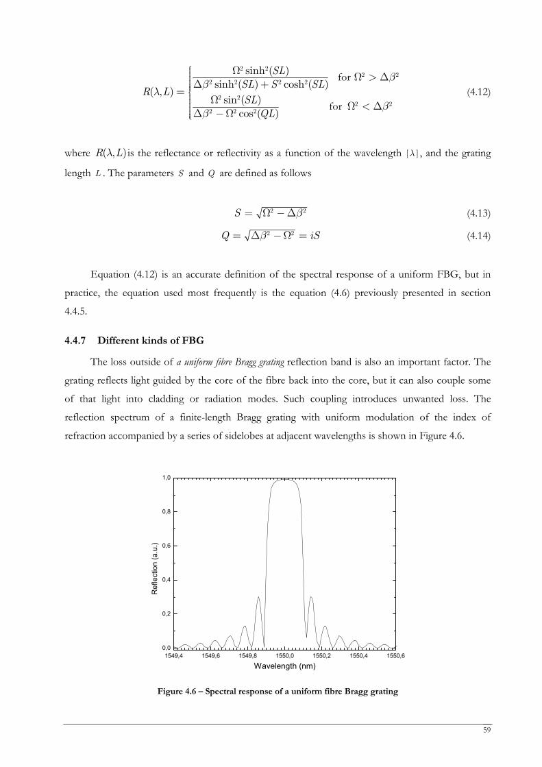
59
2 22 2
2 2 2 2
2 22 2
2 2 2
sinh ( )sinh ( ) cosh ( )
( , )sin ( )
cos ( )
SLSL S SL
R LSLQL
ββ
λβ
β
⎧⎪⎪⎪⎪⎪⎪⎨⎪⎪⎪⎪⎪⎪⎩
Ω Ω > ΔΔ +
=Ω Ω < Δ
Δ −Ω
for
for (4.12)
where ( , )R Lλ is the reflectance or reflectivity as a function of the wavelength [ ]λ , and the grating
length L . The parameters S and Q are defined as follows
2 2S β= Ω −Δ (4.13)
2 2Q iSβ= Δ −Ω = (4.14)
Equation (4.12) is an accurate definition of the spectral response of a uniform FBG, but in
practice, the equation used most frequently is the equation (4.6) previously presented in section
4.4.5.
4.4.7 Different kinds of FBG
The loss outside of a uniform fibre Bragg grating reflection band is also an important factor. The
grating reflects light guided by the core of the fibre back into the core, but it can also couple some
of that light into cladding or radiation modes. Such coupling introduces unwanted loss. The
reflection spectrum of a finite-length Bragg grating with uniform modulation of the index of
refraction accompanied by a series of sidelobes at adjacent wavelengths is shown in Figure 4.6.
1549,4 1549,6 1549,8 1550,0 1550,2 1550,4 1550,6
Wavelength (nm)
0,0
0,2
0,4
0,6
0,8
1,0
Ref
lect
ion
(a.u
.)
Figure 4.6 – Spectral response of a uniform fibre Bragg grating
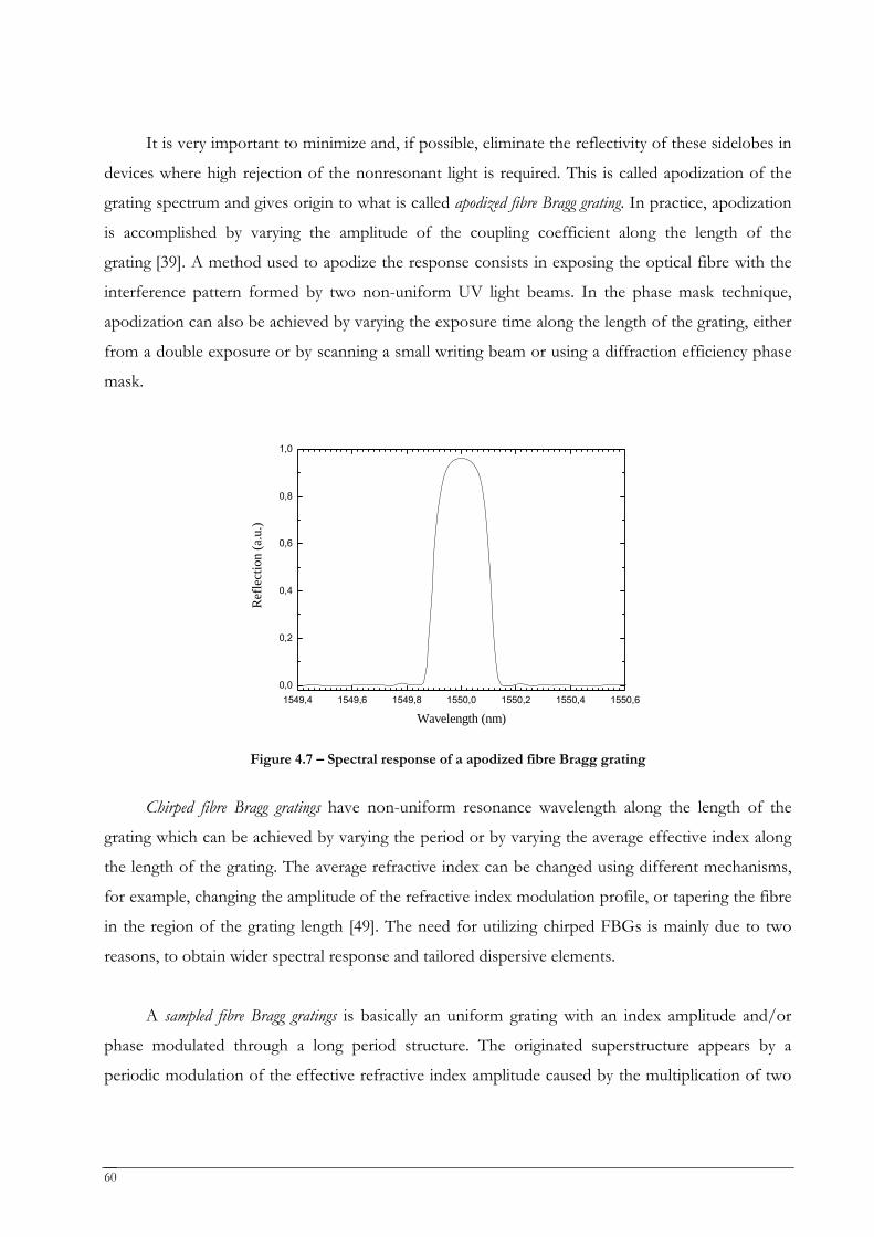
60
It is very important to minimize and, if possible, eliminate the reflectivity of these sidelobes in
devices where high rejection of the nonresonant light is required. This is called apodization of the
grating spectrum and gives origin to what is called apodized fibre Bragg grating. In practice, apodization
is accomplished by varying the amplitude of the coupling coefficient along the length of the
grating [39]. A method used to apodize the response consists in exposing the optical fibre with the
interference pattern formed by two non-uniform UV light beams. In the phase mask technique,
apodization can also be achieved by varying the exposure time along the length of the grating, either
from a double exposure or by scanning a small writing beam or using a diffraction efficiency phase
mask.
1549,4 1549,6 1549,8 1550,0 1550,2 1550,4 1550,60,0
0,2
0,4
0,6
0,8
1,0
Ref
lect
ion
(a.u
.)
Wavelength (nm)
Figure 4.7 – Spectral response of a apodized fibre Bragg grating
Chirped fibre Bragg gratings have non-uniform resonance wavelength along the length of the
grating which can be achieved by varying the period or by varying the average effective index along
the length of the grating. The average refractive index can be changed using different mechanisms,
for example, changing the amplitude of the refractive index modulation profile, or tapering the fibre
in the region of the grating length [49]. The need for utilizing chirped FBGs is mainly due to two
reasons, to obtain wider spectral response and tailored dispersive elements.
A sampled fibre Bragg gratings is basically an uniform grating with an index amplitude and/or
phase modulated through a long period structure. The originated superstructure appears by a
periodic modulation of the effective refractive index amplitude caused by the multiplication of two
61
signals of different frequencies. The reflections characteristics of SFBG make them very attractive
and useful for optical communications and fibre sensors.
Phase shift gratings are gratings with a phase shift in the modulation of the refractive index. This
phase shift in practice, splits the grating in two, thus producing two Bragg gratings that act as a
resonance cavity. The phase shift produces a narrow transmission resonance at a wavelength inside
the grating bandwidth that is defined by a amplitude and position of the phase shift [55].
4.5 Bragg gratings sensitivity to strain and temperature
The sensitivity of the gratings with temperature is a consequence of thermal expansion of the
silica matrix and thermal dependence of the refractive index. Thus, for a temperature deviation TΔ ,
the correspondent deviation in wavelength is given by,
( )1 1 effB B B
eff
nT TnT T
λ λ λ α ξ⎛ ⎞⎟⎜ ⎟⎜ ⎟⎜ ⎟⎜⎝ ⎠
∂∂ΛΔ = + Δ = + ΔΛ∂ ∂
(4.15)
where α and ξ are respectively, the thermal expansion coefficient and the thermo-optical
coefficient. In the case of silica, the thermal expansion coefficient has an absolute value of
0.55 × 10⁻⁶ C-1 and the thermo-optical coefficient a value of 6.7 × 10⁻⁶ ºC-1 [44]. This means that, the
change in the reflected wavelength as a result of temperature variations is dominated by the change
in the refractive index. On the other hand, the mechanical stress sensitivity comes simultaneously
from deformation of the silica matrix and alteration of the refractive index due to the photo-elastic
effect. The resulting change in the resonant wavelength through mechanical strain, for a longitudinal
deformation εΔ , is given by:
( )1 1 1effB B B e
eff
npnλ λ ε λ ε
ε ε⎛ ⎞⎟⎜ ⎟⎜ ⎟⎜ ⎟⎜⎝ ⎠
∂∂ΛΔ = + Δ = − ΔΛ ∂ ∂
(4.16)
where ep represents the photo-elastic constant of the fibre’s material. For a fibre with germanium
doped core, where the typical refractive index is 1.465effn = , the effective photoelastic constant is
0.22ep =− . Using these parameters, the expected sensitivity of an FBG at 1550 nm is
1.2 pm/με .
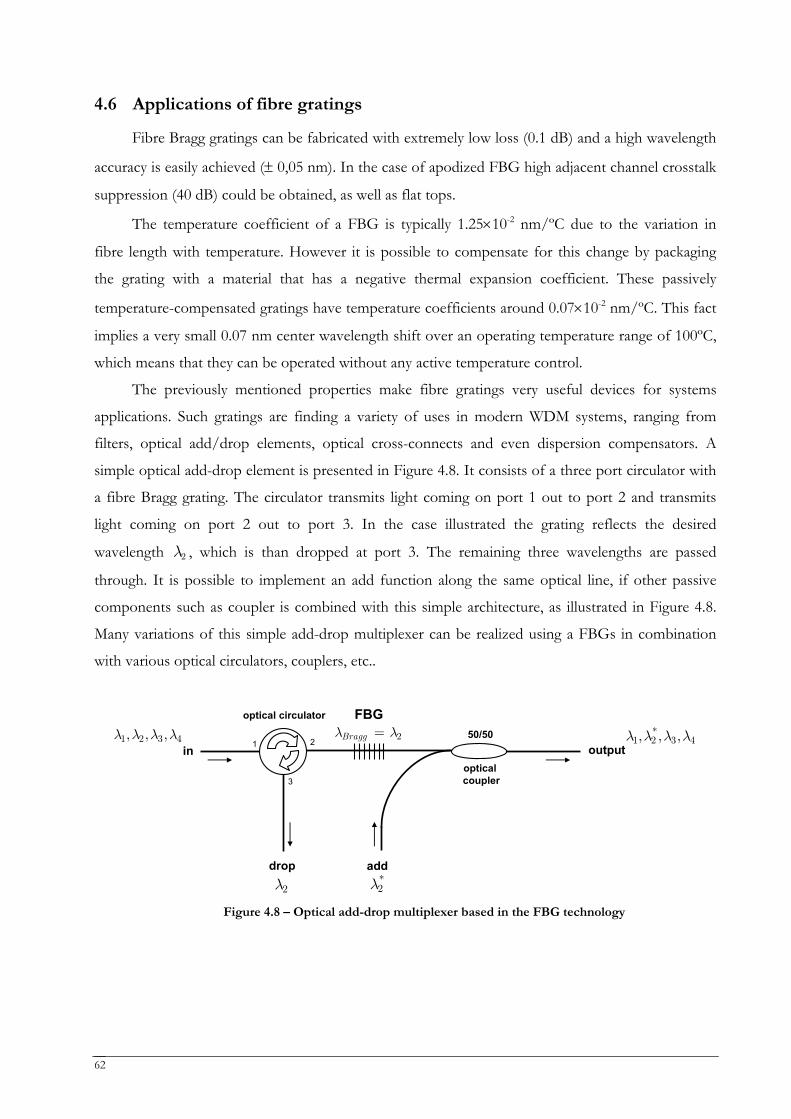
62
4.6 Applications of fibre gratings
Fibre Bragg gratings can be fabricated with extremely low loss (0.1 dB) and a high wavelength
accuracy is easily achieved (± 0,05 nm). In the case of apodized FBG high adjacent channel crosstalk
suppression (40 dB) could be obtained, as well as flat tops.
The temperature coefficient of a FBG is typically 1.25×10⁻² nm/ºC due to the variation in
fibre length with temperature. However it is possible to compensate for this change by packaging
the grating with a material that has a negative thermal expansion coefficient. These passively
temperature-compensated gratings have temperature coefficients around 0.07×10⁻² nm/ºC. This fact
implies a very small 0.07 nm center wavelength shift over an operating temperature range of 100ºC,
which means that they can be operated without any active temperature control.
The previously mentioned properties make fibre gratings very useful devices for systems
applications. Such gratings are finding a variety of uses in modern WDM systems, ranging from
filters, optical add/drop elements, optical cross-connects and even dispersion compensators. A
simple optical add-drop element is presented in Figure 4.8. It consists of a three port circulator with
a fibre Bragg grating. The circulator transmits light coming on port 1 out to port 2 and transmits
light coming on port 2 out to port 3. In the case illustrated the grating reflects the desired
wavelength 2λ , which is than dropped at port 3. The remaining three wavelengths are passed
through. It is possible to implement an add function along the same optical line, if other passive
components such as coupler is combined with this simple architecture, as illustrated in Figure 4.8.
Many variations of this simple add-drop multiplexer can be realized using a FBGs in combination
with various optical circulators, couplers, etc..
FBG
opticalcoupler
50/50
optical circulator
1 2
3
in output
drop add
1 2 3 4, , ,λ λ λ λ
2λ*2λ
*1 2 3 4, , ,λ λ λ λ2Braggλ λ=
Figure 4.8 – Optical add-drop multiplexer based in the FBG technology
63
4.7 Summary
A fibre Bragg grating consists of a periodic stack of regions of higher and lower refractive
index along an optical fibre. It has the property of reflecting light within a narrow band of
wavelengths and transmitting all wavelengths outside of that band.
Three parameters characterize a fibre Bragg grating: its strength, its period, and its length. The
first two parameters can actually be made to vary along the grating. And it is by selecting the
appropriate profiles for these two parameters that one can obtain custom-tailored spectral responses
to suit different applications.
The most popular technique for writing gratings involves "contact printing" through a phase
mask. The phase mask is itself a grating, etched in a silica substrate, with an etching depth such that
it diffracts most of the light in the +1 and -1 orders. Those two diffraction orders generate the
interference pattern. Applications of FBGs in WDM systems were also discussed.

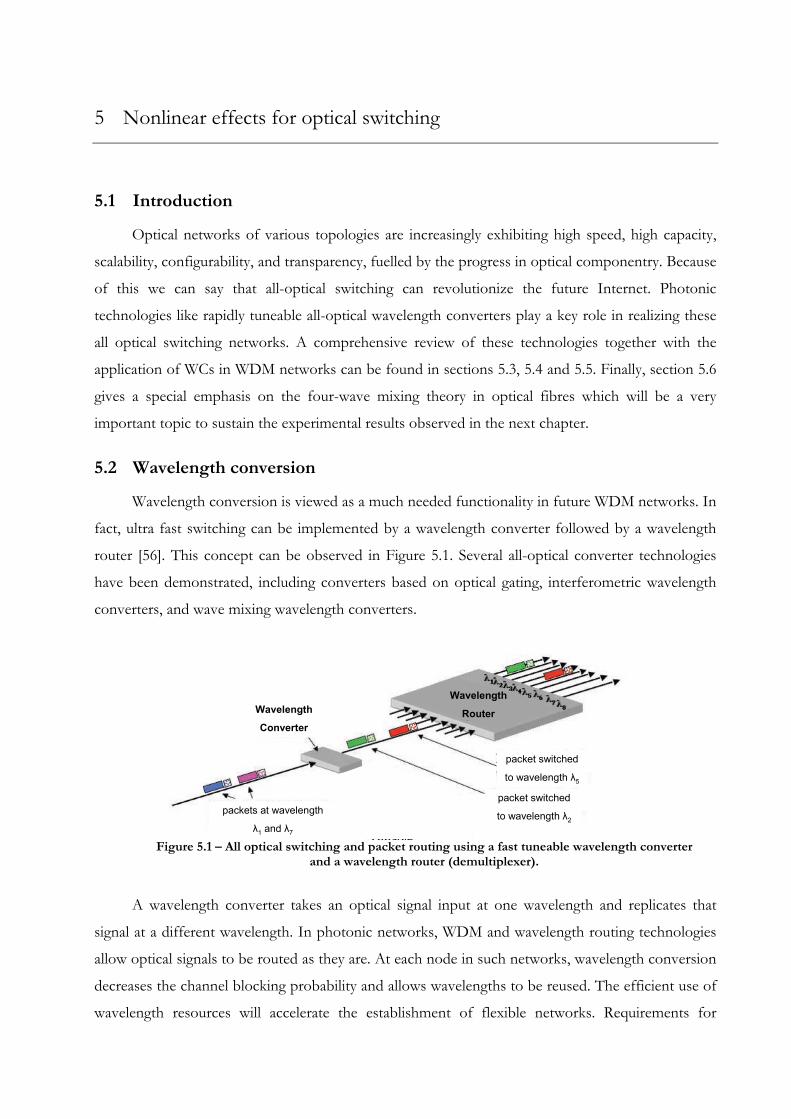
5 Nonlinear effects for optical switching
5.1 Introduction
Optical networks of various topologies are increasingly exhibiting high speed, high capacity,
scalability, configurability, and transparency, fuelled by the progress in optical componentry. Because
of this we can say that all-optical switching can revolutionize the future Internet. Photonic
technologies like rapidly tuneable all-optical wavelength converters play a key role in realizing these
all optical switching networks. A comprehensive review of these technologies together with the
application of WCs in WDM networks can be found in sections 5.3, 5.4 and 5.5. Finally, section 5.6
gives a special emphasis on the four-wave mixing theory in optical fibres which will be a very
important topic to sustain the experimental results observed in the next chapter.
5.2 Wavelength conversion
Wavelength conversion is viewed as a much needed functionality in future WDM networks. In
fact, ultra fast switching can be implemented by a wavelength converter followed by a wavelength
router [56]. This concept can be observed in Figure 5.1. Several all-optical converter technologies
have been demonstrated, including converters based on optical gating, interferometric wavelength
converters, and wave mixing wavelength converters.
packets at wavelength
λ1 and λ7
Wavelength
Converter
packet switched
to wavelength λ2
packet switched
to wavelength λ5
Wavelength
Router
packets at wavelength
λ1 and λ7
Wavelength
Converter
packet switched
to wavelength λ2
packet switched
to wavelength λ5
Wavelength
Router
Figure 5.1 – All optical switching and packet routing using a fast tuneable wavelength converter
and a wavelength router (demultiplexer).
A wavelength converter takes an optical signal input at one wavelength and replicates that
signal at a different wavelength. In photonic networks, WDM and wavelength routing technologies
allow optical signals to be routed as they are. At each node in such networks, wavelength conversion
decreases the channel blocking probability and allows wavelengths to be reused. The efficient use of
wavelength resources will accelerate the establishment of flexible networks. Requirements for
66
wavelength conversion devices are: highly efficient conversion, a high bit rate, low noise,
transparency to optical signal formats, and polarization insensitivity. Wavelength converters should
also be cascadable, have a wide input power dynamic range, and operate using the same wavelength
as the input. When these requirements meet, wavelength conversion devices can be freely used
within a network and at bridges between networks.
A wavelength converter is basically a three terminal device consisting of input, output and
control terminals. Depending on the mapping functions and the way signals are controlled,
wavelength converters can be qualified in three categories: optoelectronic, optical gating and wave
mixing.
5.2.1 Optoelectronic Wavelength Converters
The most simple wavelength conversion technique is the detection of the optical signal and
retransmission of the signal (O/E – E/O). For instance, a transmission repeater, with or without
regeneration, is an O/E-E/O wavelength converter, provided that the output wavelength is a
compliant wavelength. This technique involves an electrical routing of the signal during the
wavelength conversion process. This is a variable-input / fixed-output wavelength converter, unless
a tuneable laser or a laser array is used [57].
5.2.2 Optical Gating Wavelength Converters
This type of wavelength converters makes use of an optical device which changes its
characteristics depending on the intensity of the optical input signal. This change is monitored by a
continuous wave (CW) signal called probe and the information in the input signal is transferred to
the probe. This category includes semiconductor optical amplifier cross-gain modulation (SOA
XGM), semiconductor optical amplifier cross-phase modulation (SOA XPM), semiconductor lasers
with saturable absorption, and non-linear optical loop mirrors (NOLMs). This is a classical example
of variable-input / fixed-output wavelength converters, and we will see more of these wavelength
conversion methods as more optical gating methods are utilized [58, 59].
5.2.3 Wave-Mixing Wavelength Converters
The wavelength conversion technique based on wave-mixing offers the highest degree of
transparency. This category includes the optical-acoustic wave-mixing, optical-electric wave-mixing,
as well as nonlinear optical wave-mixing. The last method results from interactions among optical
67
waves present in a nonlinear optical material. This mechanism is sensitive to amplitude and phase
information, and is the only category of wavelength conversion method that offers strict
transparency. Four Wave Mixing (FWM) based on third order optical nonlinearities and difference
frequency generation based on second order optical nonlinearities have been demonstrated. The
utilized mixing functions are parametric, and the mapping function allows one to one mapping of an
input wavelength to an output wavelength. Therefore, the conversion process is variable-input /
variable-output. A distinctive feature in this category of wavelength converters is that they allow
simultaneous conversions of multiple input wavelengths to multiple output wavelengths [57, 58].
In the following sections each one of the wavelength conversion techniques will be discussed
in more detail.
5.3 Optoelectronic wavelength conversion
The optoelectronic approach is perhaps the simplest and most practical technique available
nowadays to realize wavelength conversion and will be presented in this chapter.
The simplest optoelectronic wavelength converter uses a detector, which converts the signal
from the optical domain to the electrical domain. Then, the signal is used to drive a source at the
desired wavelength. Prior to commercial applications of the optical fibre amplifiers, regenerators,
consisting of three main components, namely optical receiver, radio frequency (RF) amplifier, and
optical transmitter, were typically placed at a distance of 40 km in an optical link. Regenerators are
classified as 1R if they just amplify, 2R if they amplify and reshape and 3R if they amplify, reshape,
and retime [60]. A regenerator handles just one wavelength and requires a lot of maintenance. Thus,
their use in multiwavelength links will yield a high cost, low reliability, and poor upgradability, and
they are not used, unless where absolutely necessary.
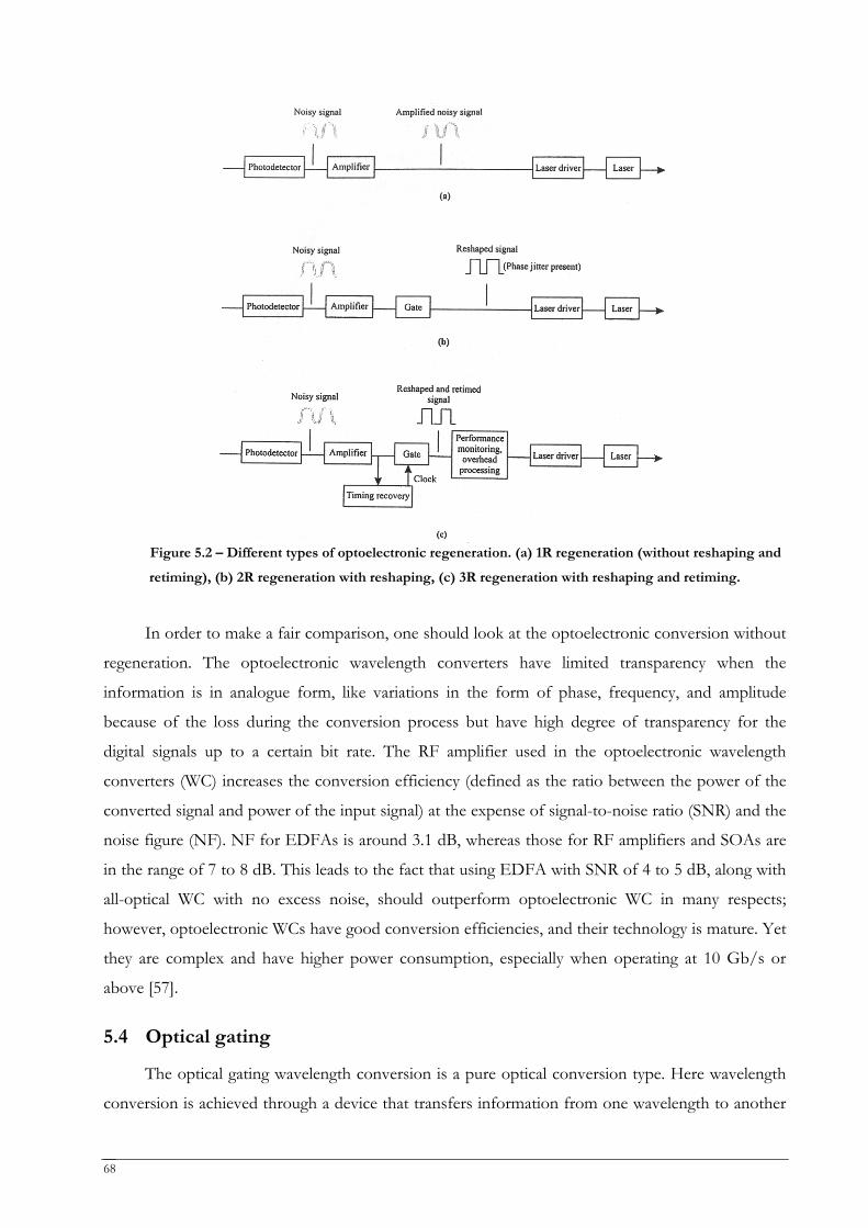
68
Figure 5.2 – Different types of optoelectronic regeneration. (a) 1R regeneration (without reshaping and
retiming), (b) 2R regeneration with reshaping, (c) 3R regeneration with reshaping and retiming.
In order to make a fair comparison, one should look at the optoelectronic conversion without
regeneration. The optoelectronic wavelength converters have limited transparency when the
information is in analogue form, like variations in the form of phase, frequency, and amplitude
because of the loss during the conversion process but have high degree of transparency for the
digital signals up to a certain bit rate. The RF amplifier used in the optoelectronic wavelength
converters (WC) increases the conversion efficiency (defined as the ratio between the power of the
converted signal and power of the input signal) at the expense of signal-to-noise ratio (SNR) and the
noise figure (NF). NF for EDFAs is around 3.1 dB, whereas those for RF amplifiers and SOAs are
in the range of 7 to 8 dB. This leads to the fact that using EDFA with SNR of 4 to 5 dB, along with
all-optical WC with no excess noise, should outperform optoelectronic WC in many respects;
however, optoelectronic WCs have good conversion efficiencies, and their technology is mature. Yet
they are complex and have higher power consumption, especially when operating at 10 Gb/s or
above [57].
5.4 Optical gating
The optical gating wavelength conversion is a pure optical conversion type. Here wavelength
conversion is achieved through a device that transfers information from one wavelength to another
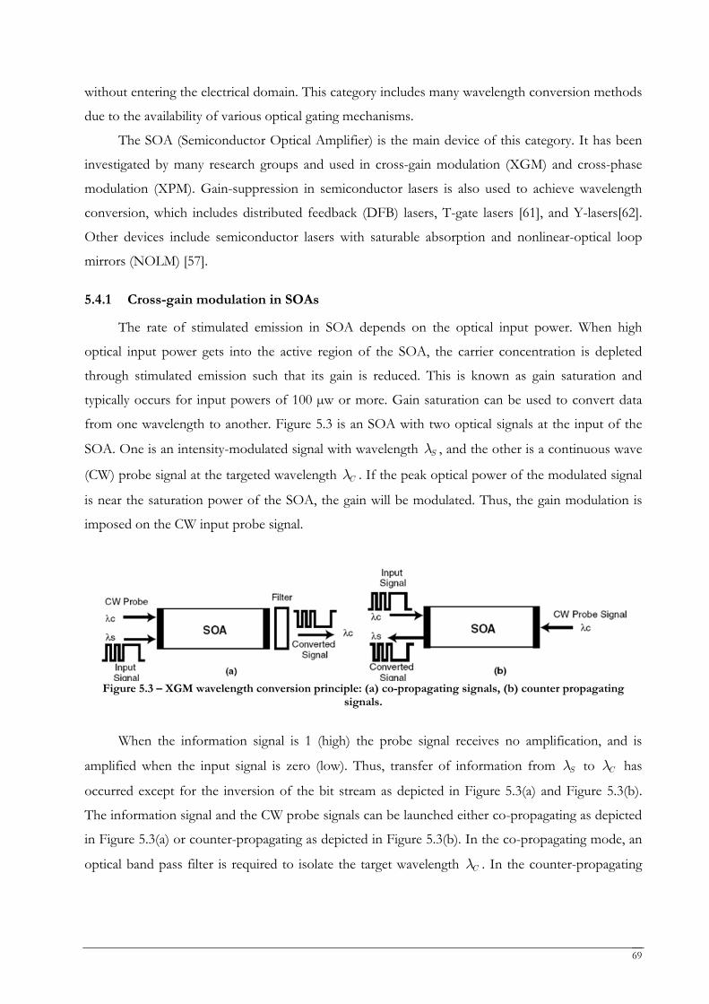
69
without entering the electrical domain. This category includes many wavelength conversion methods
due to the availability of various optical gating mechanisms.
The SOA (Semiconductor Optical Amplifier) is the main device of this category. It has been
investigated by many research groups and used in cross-gain modulation (XGM) and cross-phase
modulation (XPM). Gain-suppression in semiconductor lasers is also used to achieve wavelength
conversion, which includes distributed feedback (DFB) lasers, T-gate lasers [61], and Y-lasers[62].
Other devices include semiconductor lasers with saturable absorption and nonlinear-optical loop
mirrors (NOLM) [57].
5.4.1 Cross-gain modulation in SOAs
The rate of stimulated emission in SOA depends on the optical input power. When high
optical input power gets into the active region of the SOA, the carrier concentration is depleted
through stimulated emission such that its gain is reduced. This is known as gain saturation and
typically occurs for input powers of 100 µw or more. Gain saturation can be used to convert data
from one wavelength to another. Figure 5.3 is an SOA with two optical signals at the input of the
SOA. One is an intensity-modulated signal with wavelength Sλ , and the other is a continuous wave
(CW) probe signal at the targeted wavelength Cλ . If the peak optical power of the modulated signal
is near the saturation power of the SOA, the gain will be modulated. Thus, the gain modulation is
imposed on the CW input probe signal.
Figure 5.3 – XGM wavelength conversion principle: (a) co-propagating signals, (b) counter propagating
signals.
When the information signal is 1 (high) the probe signal receives no amplification, and is
amplified when the input signal is zero (low). Thus, transfer of information from Sλ to Cλ has
occurred except for the inversion of the bit stream as depicted in Figure 5.3(a) and Figure 5.3(b).
The information signal and the CW probe signals can be launched either co-propagating as depicted
in Figure 5.3(a) or counter-propagating as depicted in Figure 5.3(b). In the co-propagating mode, an
optical band pass filter is required to isolate the target wavelength Cλ . In the counter-propagating
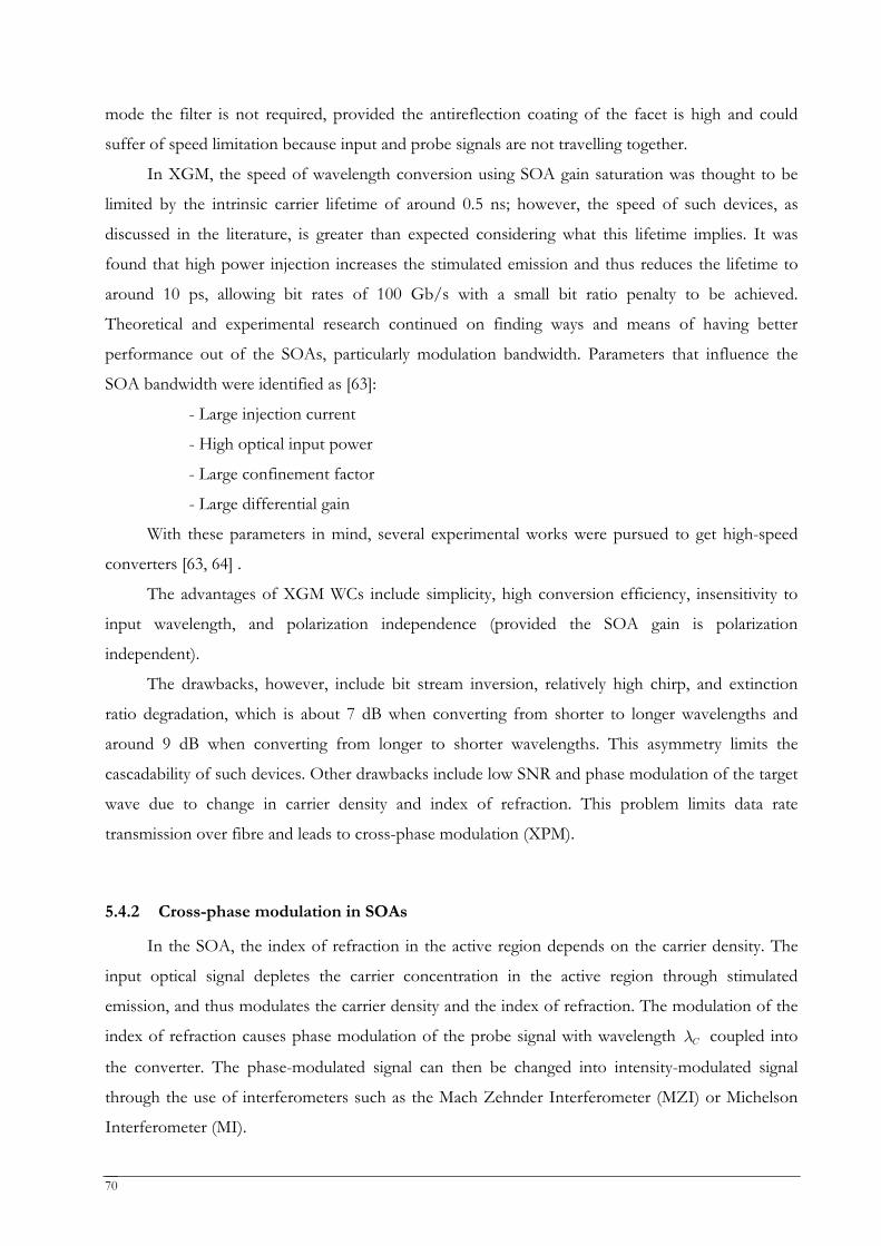
70
mode the filter is not required, provided the antireflection coating of the facet is high and could
suffer of speed limitation because input and probe signals are not travelling together.
In XGM, the speed of wavelength conversion using SOA gain saturation was thought to be
limited by the intrinsic carrier lifetime of around 0.5 ns; however, the speed of such devices, as
discussed in the literature, is greater than expected considering what this lifetime implies. It was
found that high power injection increases the stimulated emission and thus reduces the lifetime to
around 10 ps, allowing bit rates of 100 Gb/s with a small bit ratio penalty to be achieved.
Theoretical and experimental research continued on finding ways and means of having better
performance out of the SOAs, particularly modulation bandwidth. Parameters that influence the
SOA bandwidth were identified as [63]:
- Large injection current
- High optical input power
- Large confinement factor
- Large differential gain
With these parameters in mind, several experimental works were pursued to get high-speed
converters [63, 64] .
The advantages of XGM WCs include simplicity, high conversion efficiency, insensitivity to
input wavelength, and polarization independence (provided the SOA gain is polarization
independent).
The drawbacks, however, include bit stream inversion, relatively high chirp, and extinction
ratio degradation, which is about 7 dB when converting from shorter to longer wavelengths and
around 9 dB when converting from longer to shorter wavelengths. This asymmetry limits the
cascadability of such devices. Other drawbacks include low SNR and phase modulation of the target
wave due to change in carrier density and index of refraction. This problem limits data rate
transmission over fibre and leads to cross-phase modulation (XPM).
5.4.2 Cross-phase modulation in SOAs
In the SOA, the index of refraction in the active region depends on the carrier density. The
input optical signal depletes the carrier concentration in the active region through stimulated
emission, and thus modulates the carrier density and the index of refraction. The modulation of the
index of refraction causes phase modulation of the probe signal with wavelength Cλ coupled into
the converter. The phase-modulated signal can then be changed into intensity-modulated signal
through the use of interferometers such as the Mach Zehnder Interferometer (MZI) or Michelson
Interferometer (MI).
71
In the XPM, a phase change of 180º needed to operate the interferometer is obtained for a
gain variation of 4 dB, as compared with 10 dB for the XGM.[63] Different MZI or MI
configurations are shown in Figure 5.4. Figure 5.4(a) is an asymmetric MZI where the arms couplers
have different splitting ratios. When an input information signal and CW probe signal are applied to
the asymmetric configuration, power is split according to the arms-splitting ratio (β ). Consequently,
the power through each SOA leads to a phase difference between the two arms due to different
saturations of SOA1 and SOA2.
Figure 5.4 – Configurations for interferometric wavelength SOA wavelength converter: (a) an asymmetric MZI,
(b) a symmetric MZI, (c) Michelson interferometer (MI).
In Figure 5.4(b), a symmetric MZI is used. The input signal at wavelength Sλ is fed to SOA1,
which only creates an asymmetric saturation because SOA2 is not affected by this signal. A CW
probe signal at the target wavelength Cλ , which is injected as illustrated in Figure 5.4(b), will be
subject to phase modulation by the intensity modulated input signal at wavelength Sλ . In other
words, for a logic l (high) of the applied signal, the probe signal undergoes constructive interference,
thus getting 1 (high) probe signal; for logic zero (low) it undergoes destructive interference, thus
getting 0 (low) probe signal. Therefore, a converted output signal is obtained without inversion.
Another possible arrangement using MZI is to place one SOA in one of the arms to get the
required phase shift; however, this arrangement is polarization-sensitive and gives less power. Figure
5.4(c) is a Michelson interferometer with SOAs inserted into its arms. At phase difference of 180º
between the two arms, the CW probe signal at Cλ is coupled into arm1 and will be reflected back
into this arm. If the information signal at wavelength Sλ is coupled to the SOA1, additional phase
difference of 180º between arm1 and arm2 will occur due to change in the index of refraction
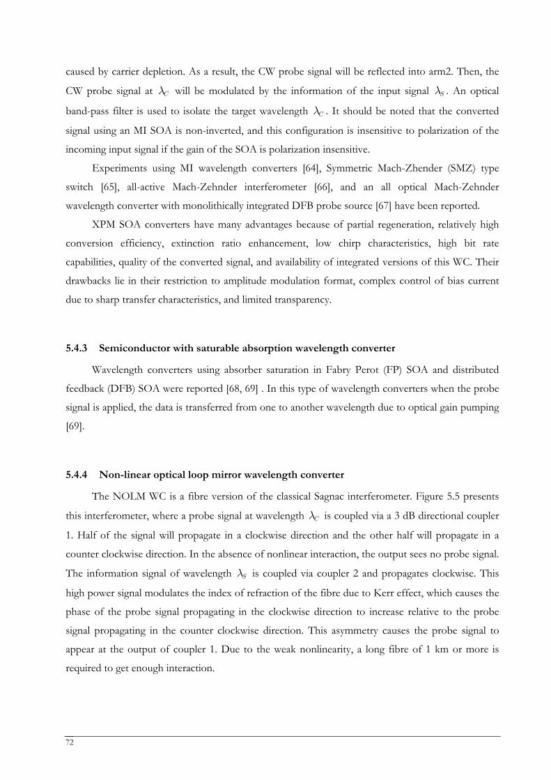
72
caused by carrier depletion. As a result, the CW probe signal will be reflected into arm2. Then, the
CW probe signal at Cλ will be modulated by the information of the input signal Sλ . An optical
band-pass filter is used to isolate the target wavelength Cλ . It should be noted that the converted
signal using an MI SOA is non-inverted, and this configuration is insensitive to polarization of the
incoming input signal if the gain of the SOA is polarization insensitive.
Experiments using MI wavelength converters [64], Symmetric Mach-Zhender (SMZ) type
switch [65], all-active Mach-Zehnder interferometer [66], and an all optical Mach-Zehnder
wavelength converter with monolithically integrated DFB probe source [67] have been reported.
XPM SOA converters have many advantages because of partial regeneration, relatively high
conversion efficiency, extinction ratio enhancement, low chirp characteristics, high bit rate
capabilities, quality of the converted signal, and availability of integrated versions of this WC. Their
drawbacks lie in their restriction to amplitude modulation format, complex control of bias current
due to sharp transfer characteristics, and limited transparency.
5.4.3 Semiconductor with saturable absorption wavelength converter
Wavelength converters using absorber saturation in Fabry Perot (FP) SOA and distributed
feedback (DFB) SOA were reported [68, 69] . In this type of wavelength converters when the probe
signal is applied, the data is transferred from one to another wavelength due to optical gain pumping
[69].
5.4.4 Non-linear optical loop mirror wavelength converter
The NOLM WC is a fibre version of the classical Sagnac interferometer. Figure 5.5 presents
this interferometer, where a probe signal at wavelength Cλ is coupled via a 3 dB directional coupler
1. Half of the signal will propagate in a clockwise direction and the other half will propagate in a
counter clockwise direction. In the absence of nonlinear interaction, the output sees no probe signal.
The information signal of wavelength Sλ is coupled via coupler 2 and propagates clockwise. This
high power signal modulates the index of refraction of the fibre due to Kerr effect, which causes the
phase of the probe signal propagating in the clockwise direction to increase relative to the probe
signal propagating in the counter clockwise direction. This asymmetry causes the probe signal to
appear at the output of coupler 1. Due to the weak nonlinearity, a long fibre of 1 km or more is
required to get enough interaction.
73
Figure 5.5 – NOLM wavelength converters: (a) fibre loop, (b) SOA as the nonlinear medium
Nonlinearity can effectively be increased through insertion of SOA in the loop as illustrated in
Figure 5.5(b). The SOA is placed asymmetrically with respect to the loop centre. Coupler 1 splits a
probe signal at Cλ into two equal signals; one propagates clockwise and the other propagates
counter clockwise. An information signal at Sλ is coupled to the loop through coupler 2, saturates
the SOA gain, and induces a change in the index of refraction. The two probe signals are subject to
different phase shifts because one of them reaches the SOA before saturation and the other reaches
the SOA after saturation. When the two signals arrive at coupler 1, they interfere and generate an
output pulse at the output of coupler 1; thus conversion is achieved. This device is known as
terahertz optical asymmetric demultiplexer (TOAD). This device has been operated as a 40Gb/s
wavelength converter and a simultaneous 4:1 demultiplexer [70].
Optical nonlinearity can also be enhanced through increased concentration of germanium in
the core of a dispersion shifted fibre (DSF), thus getting highly nonlinear dispersion shifted fibre
(HNL-DSF). The high nonlinear coefficient of the HNL-DSF makes the fibre much shorter and
thus more compact than the other designs. A 50 m long HNL-DSF was constructed and
demonstration of wavelength conversion of 500 fs pulse trains, over a bandwidth of 26 nm, with
peak power of 4 W was reported [71].
NOLM WCs have less noise because the wavelength conversion efficiency is a nonlinear
function of the input signal power. However, the NOLM requires short pulses compared with the
bit period, and suffers from stability problems.
5.5 Wave Mixing Wavelength Conversion
Certain materials change their properties when subjected to electric fields. The parameter that
is influenced is the index of refraction. The index of refraction change due to the applied electric
field is called Pockels effect, and the index of refraction change due to the square of the applied
electric field is called Kerr effect. Thus, applying light with certain intensity will cause nonlinearity in
the optical medium due to Kerr effect. Four-wave mixing (FWM) is a type of Kerr effect that occurs
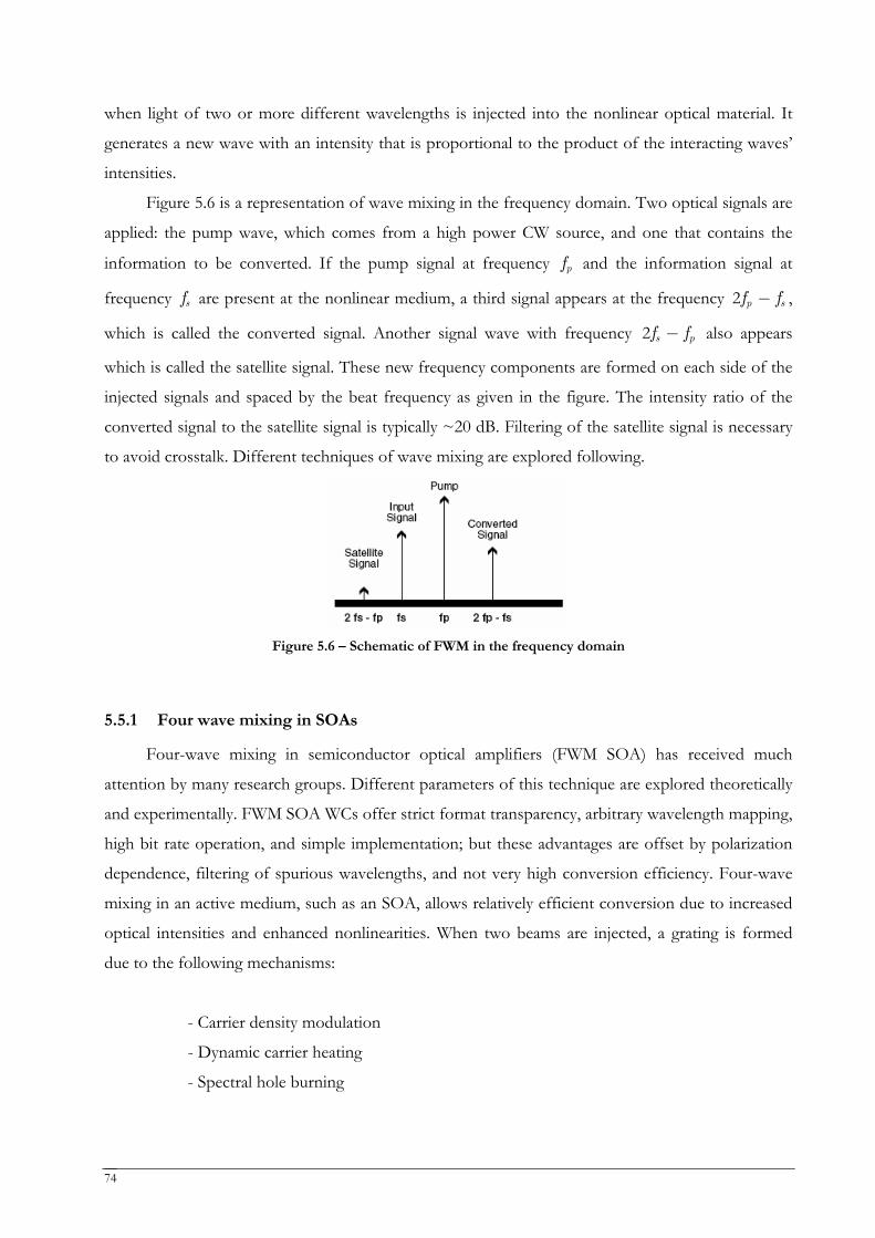
74
when light of two or more different wavelengths is injected into the nonlinear optical material. It
generates a new wave with an intensity that is proportional to the product of the interacting waves’
intensities.
Figure 5.6 is a representation of wave mixing in the frequency domain. Two optical signals are
applied: the pump wave, which comes from a high power CW source, and one that contains the
information to be converted. If the pump signal at frequency pf and the information signal at
frequency sf are present at the nonlinear medium, a third signal appears at the frequency p sf f−2 ,
which is called the converted signal. Another signal wave with frequency s pf f−2 also appears
which is called the satellite signal. These new frequency components are formed on each side of the
injected signals and spaced by the beat frequency as given in the figure. The intensity ratio of the
converted signal to the satellite signal is typically ~20 dB. Filtering of the satellite signal is necessary
to avoid crosstalk. Different techniques of wave mixing are explored following.
Figure 5.6 – Schematic of FWM in the frequency domain
5.5.1 Four wave mixing in SOAs
Four-wave mixing in semiconductor optical amplifiers (FWM SOA) has received much
attention by many research groups. Different parameters of this technique are explored theoretically
and experimentally. FWM SOA WCs offer strict format transparency, arbitrary wavelength mapping,
high bit rate operation, and simple implementation; but these advantages are offset by polarization
dependence, filtering of spurious wavelengths, and not very high conversion efficiency. Four-wave
mixing in an active medium, such as an SOA, allows relatively efficient conversion due to increased
optical intensities and enhanced nonlinearities. When two beams are injected, a grating is formed
due to the following mechanisms:
- Carrier density modulation
- Dynamic carrier heating
- Spectral hole burning
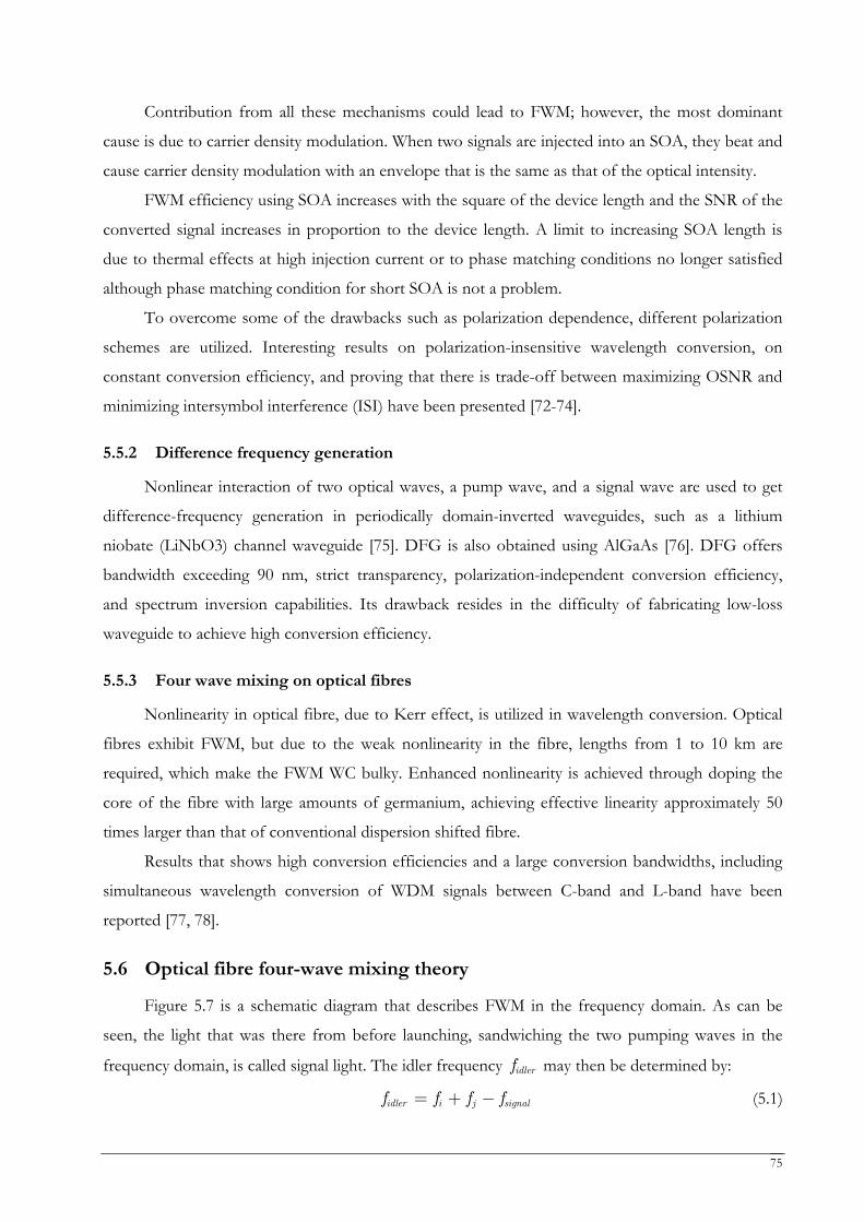
75
Contribution from all these mechanisms could lead to FWM; however, the most dominant
cause is due to carrier density modulation. When two signals are injected into an SOA, they beat and
cause carrier density modulation with an envelope that is the same as that of the optical intensity.
FWM efficiency using SOA increases with the square of the device length and the SNR of the
converted signal increases in proportion to the device length. A limit to increasing SOA length is
due to thermal effects at high injection current or to phase matching conditions no longer satisfied
although phase matching condition for short SOA is not a problem.
To overcome some of the drawbacks such as polarization dependence, different polarization
schemes are utilized. Interesting results on polarization-insensitive wavelength conversion, on
constant conversion efficiency, and proving that there is trade-off between maximizing OSNR and
minimizing intersymbol interference (ISI) have been presented [72-74].
5.5.2 Difference frequency generation
Nonlinear interaction of two optical waves, a pump wave, and a signal wave are used to get
difference-frequency generation in periodically domain-inverted waveguides, such as a lithium
niobate (LiNbO3) channel waveguide [75]. DFG is also obtained using AlGaAs [76]. DFG offers
bandwidth exceeding 90 nm, strict transparency, polarization-independent conversion efficiency,
and spectrum inversion capabilities. Its drawback resides in the difficulty of fabricating low-loss
waveguide to achieve high conversion efficiency.
5.5.3 Four wave mixing on optical fibres
Nonlinearity in optical fibre, due to Kerr effect, is utilized in wavelength conversion. Optical
fibres exhibit FWM, but due to the weak nonlinearity in the fibre, lengths from 1 to 10 km are
required, which make the FWM WC bulky. Enhanced nonlinearity is achieved through doping the
core of the fibre with large amounts of germanium, achieving effective linearity approximately 50
times larger than that of conventional dispersion shifted fibre.
Results that shows high conversion efficiencies and a large conversion bandwidths, including
simultaneous wavelength conversion of WDM signals between C-band and L-band have been
reported [77, 78].
5.6 Optical fibre four-wave mixing theory
Figure 5.7 is a schematic diagram that describes FWM in the frequency domain. As can be
seen, the light that was there from before launching, sandwiching the two pumping waves in the
frequency domain, is called signal light. The idler frequency idlerf may then be determined by:
idler i j signalf f f f= + − (5.1)
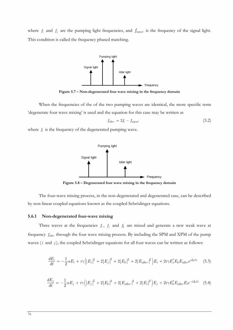
76
where if and jf are the pumping light frequencies, and signalf is the frequency of the signal light.
This condition is called the frequency phased matching.
Figure 5.7 – Non-degenerated four wave mixing in the frequency domain
When the frequencies of the of the two pumping waves are identical, the more specific term
‘degenerate four wave mixing’ is used and the equation for this case may be written as
2idler i signalf f f= − (5.2)
where if is the frequency of the degenerated pumping wave.
Figure 5.8 – Degenerated four wave mixing in the frequency domain
The four-wave mixing process, in the non-degenerated and degenerated case, can be described
by non-linear coupled equations known as the coupled Schrödinger equations.
5.6.1 Non-degenerated four-wave mixing
Three waves at the frequencies if , jf and kf are mixed and generate a new weak wave at
frequency idlerf through the four wave mixing process. By including the SPM and XPM of the pump
waves ( i and j ), the coupled Schrödinger equations for all four waves can be written as follows:
( )22 2 2 *12 2 2 2
2i i z
i i j i jk idler k idlerdE
E i E E E E E i E E E edt
βα γ γ Δ= − + + + + + (5.3)
( )2 2 2 2 *12 2 2 2
2j i z
j j i j ik idler k idlerdE
E i E E E E E i E E E edt
βα γ γ − Δ= − + + + + + (5.4)
77
( )22 2 2 *12 2 2 2
2k i z
i j i jk k idler k idlerdE
E i E E E E E i E E E edt
βα γ γ − Δ= − + + + + + (5.5)
( )22 2 2 *12 2 2 2
2idler i z
idler idler i j k idler i j kdE
E i E E E E E i E E E edt
βα γ γ − Δ= − + + + + + (5.6)
where z is the longitudinal coordinate of the fibre, α is the attenuation coefficient of the
fibre, iE , jE , kE and idlerE are the electric fields of the pumping ( i , j ), signal (k ) and idler (or new)
waves. The terms on the right hand side of equations (5.3) to (5.6) correspond to signal loss, self-
phase modulation (SPM) and the cross-phase modulation (XPM), respectively. The non-linear
coefficient γ is obtained by:
22 22 k
k eff eff
n fnA cA
ππγλ
= = (5.7)
where c is the speed of the light in the vacuum, 2n is the non-linear refractive index which
is related to the refractive index of the fibre core ( )n and to the third-order non-linear susceptibility
(3)( )χ by [79]:
2
(3)2
2
48n cnπ χ= (5.8)
effA is the effective fibre core area for the guided 11H mode, and is given by:
( )
( )
22
4
,
,
reff
r
F r r d dr
AF r r d dr
θ
θ
θ θ
θ θ
⎡ ⎤⎢ ⎥⎢ ⎥⎢ ⎥⎣ ⎦=∫ ∫
∫ ∫ (5.9)
where ( , )F r θ is the cross sectional distribution of the fundamental mode 11H . The term βΔ in the
coupled Schrödinger equations is the propagation constant difference, also called the phase
matching factor [79, 80], and is known as
i jidler kβ β β β βΔ = + − −
22 1( )( ) ( ) ( )
2
effLi jk ki j i jk k k k k
eff
f f dD ef f f f D f P P P
c c d L
αλπλβ λ γλ α
−⎛ ⎞⎡ ⎤⎡ ⎤ ⎟⎜⎢ ⎥ ⎟⎢ ⎥ ⎜ ⎟⎜⎢ ⎥ ⎟⎢ ⎥ ⎜ ⎟⎝ ⎠⎣ ⎦⎢ ⎥⎣ ⎦
+ −Δ = − − + − − + − (5.10)
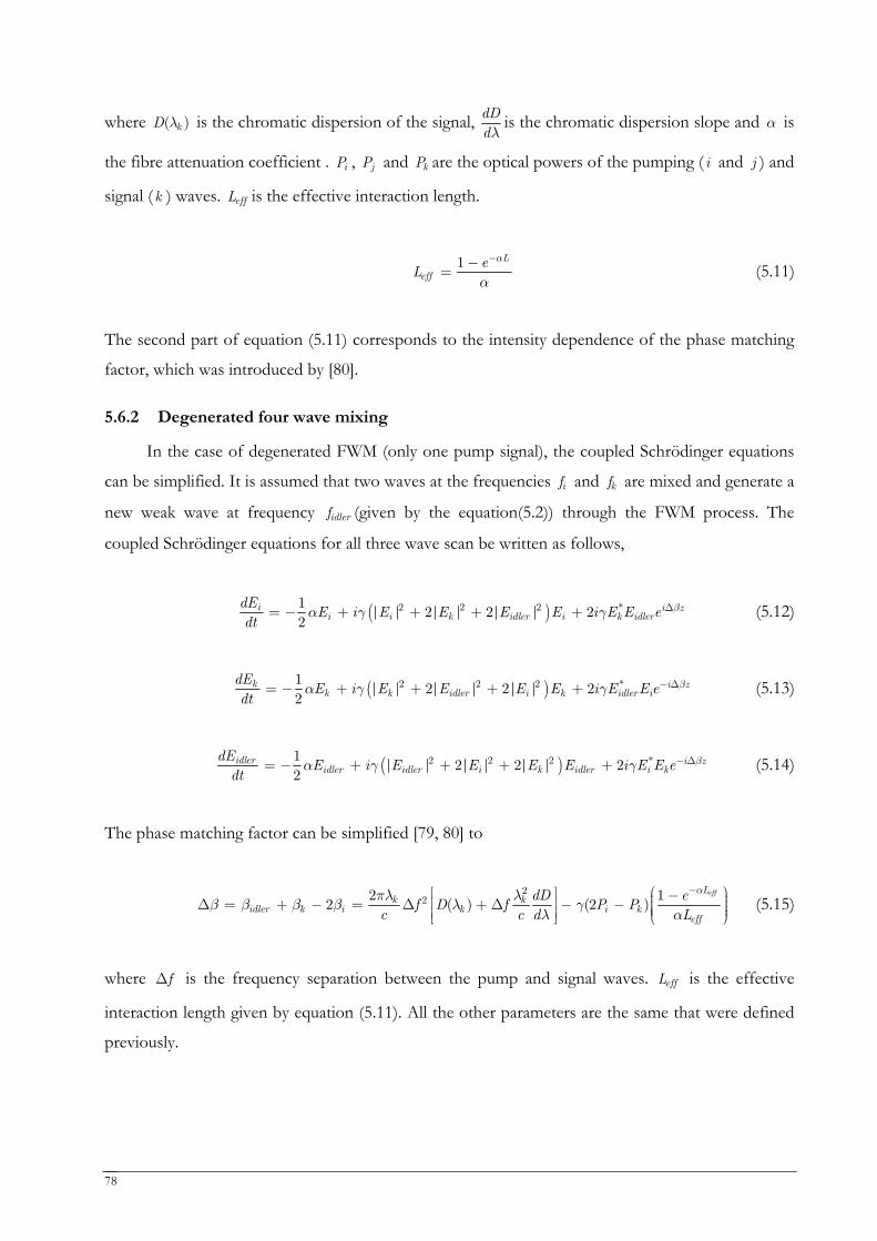
78
where ( )kD λ is the chromatic dispersion of the signal, dDdλ
is the chromatic dispersion slope and α is
the fibre attenuation coefficient . iP , jP and kP are the optical powers of the pumping ( i and j ) and
signal (k ) waves. effL is the effective interaction length.
1 L
effe
Lα
α
−−= (5.11)
The second part of equation (5.11) corresponds to the intensity dependence of the phase matching
factor, which was introduced by [80].
5.6.2 Degenerated four wave mixing
In the case of degenerated FWM (only one pump signal), the coupled Schrödinger equations
can be simplified. It is assumed that two waves at the frequencies if and kf are mixed and generate a
new weak wave at frequency idlerf (given by the equation(5.2)) through the FWM process. The
coupled Schrödinger equations for all three wave scan be written as follows,
( )2 2 2 *12 2 2
2i i z
i i k idler i k idlerdE
E i E E E E i E E edt
βα γ γ Δ= − + + + + (5.12)
( )2 2 2 *12 2 2
2k i z
k k idler i k idler idE
E i E E E E i E E edt
βα γ γ − Δ= − + + + + (5.13)
( )2 2 2 *12 2 2
2idler i z
idler idler i k idler i kdE
E i E E E E i E E edt
βα γ γ − Δ= − + + + + (5.14)
The phase matching factor can be simplified [79, 80] to
2
22 12 ( ) (2 )
effLk k
idler k i k i keff
dD ef D f P P
c c d L
απλ λβ β β β λ γ
λ α
−⎛ ⎞⎡ ⎤ − ⎟⎜⎢ ⎥ ⎟Δ = + − = Δ + Δ − − ⎜ ⎟⎜ ⎟⎜⎢ ⎥ ⎝ ⎠⎣ ⎦ (5.15)
where fΔ is the frequency separation between the pump and signal waves. effL is the effective
interaction length given by equation (5.11). All the other parameters are the same that were defined
previously.
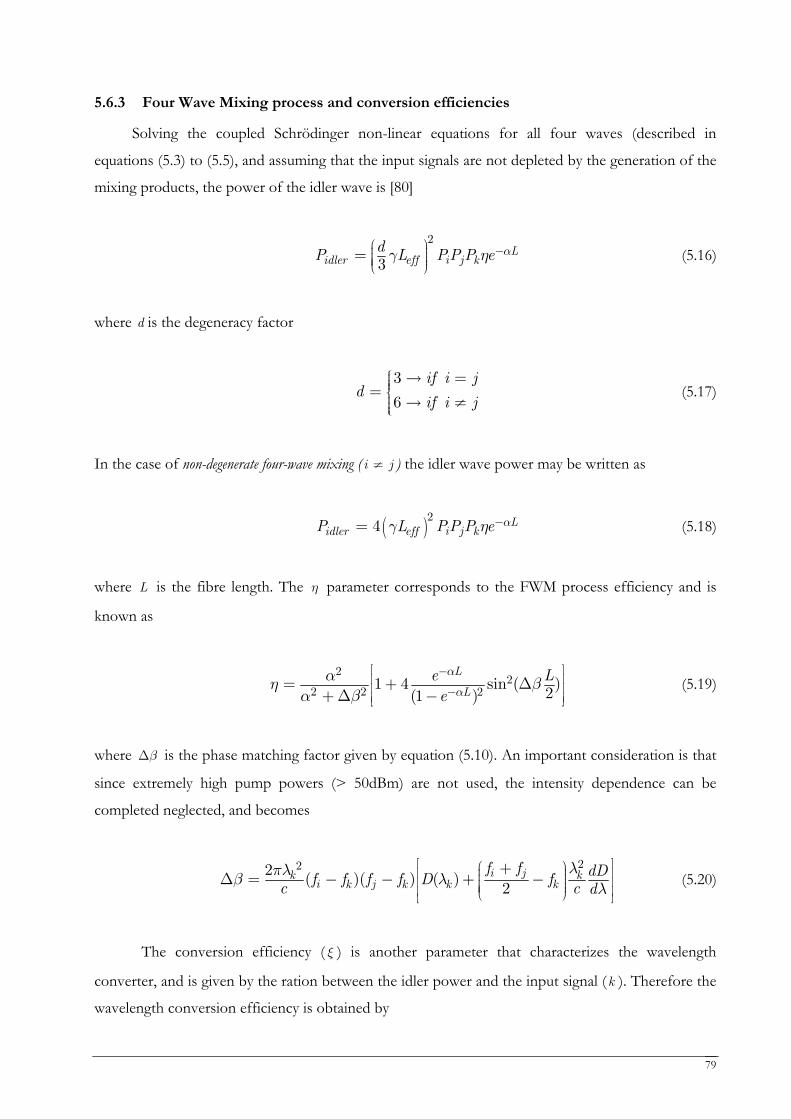
79
5.6.3 Four Wave Mixing process and conversion efficiencies
Solving the coupled Schrödinger non-linear equations for all four waves (described in
equations (5.3) to (5.5), and assuming that the input signals are not depleted by the generation of the
mixing products, the power of the idler wave is [80]
2
3L
i jidler eff kdP L PP P e αγ η −⎛ ⎞⎟⎜ ⎟⎜ ⎟⎜ ⎟⎜⎝ ⎠
= (5.16)
where d is the degeneracy factor
3
6
if i jd
if i j
⎧⎪⎪⎪⎨⎪⎪⎪⎩
→ ==
→ ≠ (5.17)
In the case of non-degenerate four-wave mixing ( i j≠ ) the idler wave power may be written as
( )24 Li jidler eff kP L PP P e αγ η −= (5.18)
where L is the fibre length. The η parameter corresponds to the FWM process efficiency and is
known as
2
22 2 21 4 sin ( )
2(1 )
L
Le Le
α
ααη β
α β
−
−
⎡ ⎤⎢ ⎥⎢ ⎥⎢ ⎥⎣ ⎦
= + Δ+Δ −
(5.19)
where βΔ is the phase matching factor given by equation (5.10). An important consideration is that
since extremely high pump powers (> 50dBm) are not used, the intensity dependence can be
completed neglected, and becomes
222
( )( ) ( )2
i jk ki jk k k k
f f dDf f f f D fc c dλπλβ λ λ
⎡ ⎤⎛ ⎞⎟⎜⎢ ⎥⎟⎜ ⎟⎢ ⎥⎜ ⎟⎜ ⎟⎜⎢ ⎥⎝ ⎠⎣ ⎦
+Δ = − − + − (5.20)
The conversion efficiency ( ξ ) is another parameter that characterizes the wavelength
converter, and is given by the ration between the idler power and the input signal (k ). Therefore the
wavelength conversion efficiency is obtained by
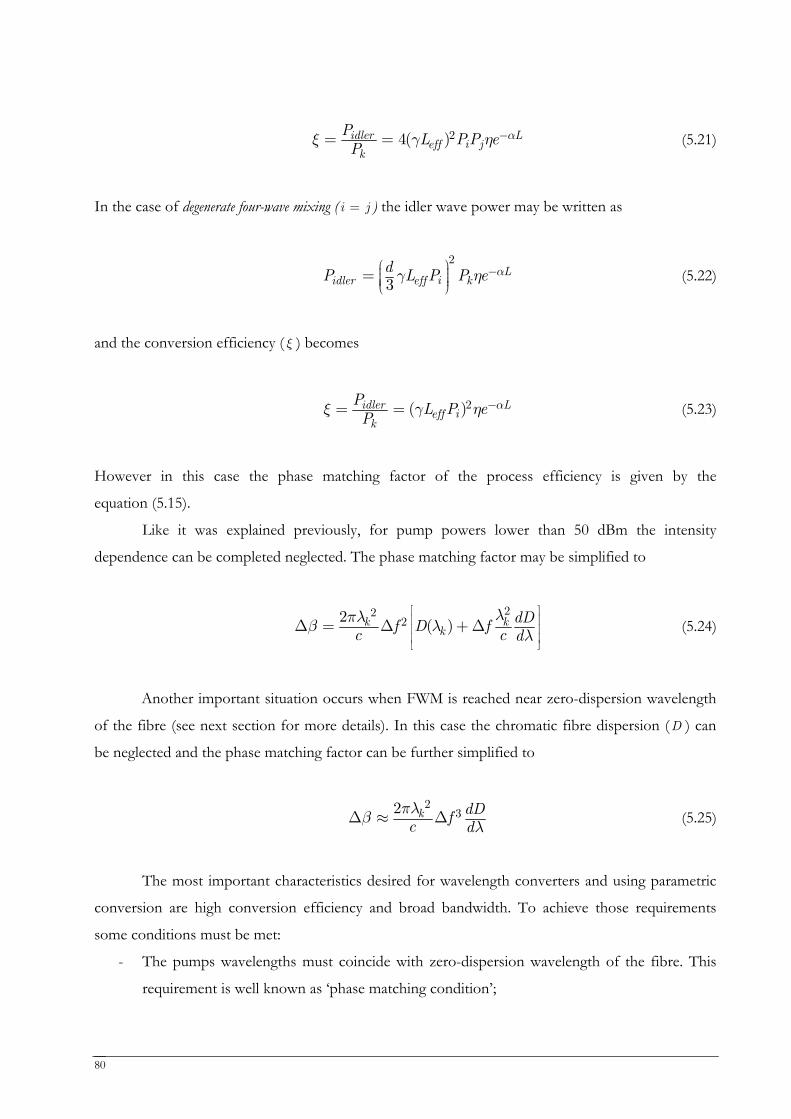
80
24( )idler Li jeff
k
P L PP eP
αξ γ η −= = (5.21)
In the case of degenerate four-wave mixing ( i j= ) the idler wave power may be written as
2
3L
iidler eff kdP L P P e αγ η −⎛ ⎞⎟⎜ ⎟⎜ ⎟⎜ ⎟⎜⎝ ⎠
= (5.22)
and the conversion efficiency ( ξ ) becomes
2( )idler Lieff
k
PL P e
Pαξ γ η −= = (5.23)
However in this case the phase matching factor of the process efficiency is given by the
equation (5.15).
Like it was explained previously, for pump powers lower than 50 dBm the intensity
dependence can be completed neglected. The phase matching factor may be simplified to
22
22( )k kk
dDf D fc c dλπλβ λ λ
⎡ ⎤⎢ ⎥⎢ ⎥⎢ ⎥⎣ ⎦
Δ = Δ +Δ (5.24)
Another important situation occurs when FWM is reached near zero-dispersion wavelength
of the fibre (see next section for more details). In this case the chromatic fibre dispersion (D ) can
be neglected and the phase matching factor can be further simplified to
2
32 k dDfc dπλβ λΔ ≈ Δ (5.25)
The most important characteristics desired for wavelength converters and using parametric
conversion are high conversion efficiency and broad bandwidth. To achieve those requirements
some conditions must be met:
- The pumps wavelengths must coincide with zero-dispersion wavelength of the fibre. This
requirement is well known as ‘phase matching condition’;
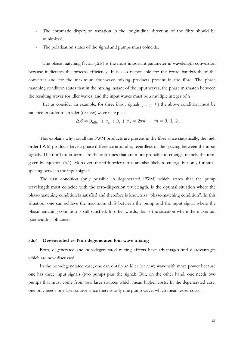
81
- The chromatic dispersion variation in the longitudinal direction of the fibre should be
minimized;
- The polarization states of the signal and pumps must coincide.
The phase matching factor ( βΔ ) is the most important parameter in wavelength conversion
because it dictates the process efficiency. It is also responsible for the broad bandwidth of the
converter and for the maximum four-wave mixing products present in the fibre. The phase
matching condition states that in the mixing instant of the input waves, the phase mismatch between
the resulting waves (or idler waves) and the input waves must be a multiple integer of 2π .
Let us consider an example, for three input signals ( i , j , k ) the above condition must be
satisfied in order to an idler (or new) wave take place:
2 0, 1, 2i jidler k m mβ β β β β πΔ = + + + = → = …
This explains why not all the FWM products are present in the fibre since statistically, the high
order FWM products have a phase difference around π, regardless of the spacing between the input
signals. The third order terms are the only ones that are more probable to emerge, namely the term
given by equation (5.1). Moreover, the fifth order terms are also likely to emerge but only for small
spacing between the input signals.
The first condition (only possible in degenerated FWM) which states that the pump
wavelength must coincide with the zero-dispersion wavelength, is the optimal situation where the
phase-matching condition is satisfied and therefore is known as “phase-matching condition”. In this
situation, one can achieve the maximum shift between the pump and the input signal where the
phase-matching condition is still satisfied. In other words, this is the situation where the maximum
bandwidth is obtained.
5.6.4 Degenerated vs. Non-degenerated four wave mixing
Both, degenerated and non-degenerated mixing effects have advantages and disadvantages
which are now discussed.
In the non-degenerated case, one can obtain an idler (or new) wave with more power because
one has three input signals (two pumps plus the signal). But, on the other hand, one needs two
pumps that must come from two laser sources which mean higher costs. In the degenerated case,
one only needs one laser source since there is only one pump wave, which mean lesser costs.
82
Another significant advantage of the non-degenerated case is that one needs a smaller fibre
length for the non-linear effects to emerge. One important disadvantage is that the “phase-matching
condition” is never completely satisfied since both pumps cannot coincide with the zero-dispersion
wavelength of the fibre (by definition, when both pumps coincide at the same wavelength, one is in
the degenerated case). Hence, one can never achieve the maximum efficiency and bandwidth with
the non-degenerated case.
In the degenerated case, since one has only one pump wave, the pump can be placed in the
zero-dispersion of the fibre in order to obtain the maximum efficiency and bandwidth. This is one
of the major advantages of the degenerated case.
Another of the major disadvantages of the non-degenerated case is that since one has three
inputs signals, one will obtain more FWM products which will cause interferences and an eventual
degradation of the wavelength converter.
5.7 Summary
As could be seen optical wavelength conversion can enhance the performance of wavelength
division multiplexing (WDM) optical networks namely the optical switching topic, and it has been a
subject of intensive studies in recent years. This chapter gives an overview of the different
technologies employed in the development of wavelength converters. Optoelectronic, optical gating
and wave-mixing techniques were described. Finally the degenerate and non-degenerate four wave
mixing processes in optical fibres were study and a comparison between the two kinds of this wave-
mixing effect was discussed.
6 Experimental studies in optical switching and wavelength conversion
6.1 Introduction
Optical Switching is a fundamental functionality in the next generation of optical networks in
order to support a sustained growth needed for bandwidth enhancement in modern communication
networks. In order to sustain the growing demands for the increasing wideband, the optical
communication networks have undergone a great evolution during the last years. The switching
networks based on wavelength division multiplexing (WDM), has been shown to be a reliable
solution to this problem. The evolution of this kind of networks requires research and development
of optical devices that allow all-optical switching and at the same time the capacity of control and
route the optical channels in a transparent way. These functionalities can be performed in a DWDM
network by optical fibre devices such as optical multiplexers/demultiplexers and optical cross-
connects. The application of fibre Bragg gratings within this context is explored here through
experimental work. In sections 6.2 to 6.5 four different techniques are presented where tuneability is
achieved using thermal and mechanical tuning of FBGs.
Nonlinear optics effects based schemes, namely wavelength conversion relying in the four
wave mixing effect, that could be also used in modern all optical networks to improve wavelength
switching capabilities are also experimentally implemented and its applications are discussed in
sections 6.6 to 6.8.
6.2 Fibre Bragg gratings based optical switching techniques
Optical fibre Bragg gratings, are optical filters that work in transmission in a similar way to the
electrical band-pass filters, but as explained previously in Chapter 4 , they have an intrinsic property
that allows the back reflection of an wavelength band that could be redirected to another optical
path. That is the capacity that makes the optical fibre Bragg grating an interesting device in the all-
optical networks ambit.
When the WDM channels tuning is done through gratings several techniques may be
explored: inducing temperature variation with a thermoelectric cooler (Peltier element), thin film
deposition (of Ti and Pt) over a FBG, or pumping a Bragg grating using a high power laser diode. It
is also possible to induce tuning with a piezoelectric element (PZT) that applies a mechanical
deformation to the optical filter.
Another alternative to the optical switching techniques described previously is the one based
in non-linear effects, namely, the four-wave mixing wavelength conversion.
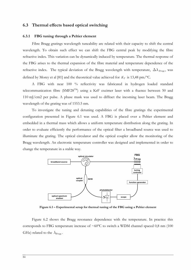
84
6.3 Thermal effects based optical switching
6.3.1 FBG tuning through a Peltier element
Fibre Bragg gratings wavelength tuneability are related with their capacity to shift the central
wavelength. To obtain such effect we can shift the FBG central peak by modifying the fibre
refractive index. This variation can be dynamically induced by temperature. The thermal response of
the FBG arises to the thermal expansion of the fibre material and temperature dependence of the
refractive index. The typical deviation of the Bragg wavelength with temperature, BraggλΔ , was
defined by Morey et al [81] and the theoretical value achieved for TK is 13,48 pm/ºC.
A FBG with near 100 % reflectivity was fabricated in hydrogen loaded standard
telecommunication fibre (SMF28TM) using a KrF excimer laser with a fluence between 50 and
110 mJ/cm2 per pulse. A phase mask was used to diffract the incoming laser beam. The Bragg
wavelength of the grating was of 1553.5 nm.
To investigate the tuning and detuning capabilities of the fibre gratings the experimental
configuration presented in Figure 6.1 was used. A FBG is placed over a Peltier element and
embedded in a thermal mass which allows a uniform temperature distribution along the grating. In
order to evaluate efficiently the performance of the optical filter a broadband source was used to
illuminate the grating. The optical circulator and the optical coupler allow the monitoring of the
Bragg wavelength. An electronic temperature controller was designed and implemented in order to
change the temperature in a stable way. FBGλBragg
scope
broadband source
optical spectrumanaliser
function generator
tuningcontroler
opticalcoupler
50/50
photodetector
optical circulator
Figure 6.1 – Experimental setup for thermal tuning of the FBG using a Peltier element
Figure 6.2 shows the Bragg resonance dependence with the temperature. In practice this
corresponds to FBG temperature increase of ~60ºC to switch a WDM channel spaced 0,8 nm (100
GHz) related to the Braggλ .
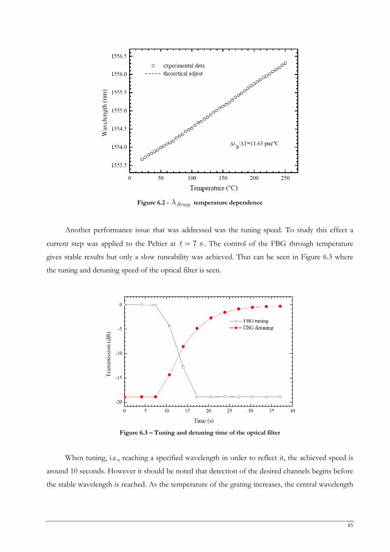
85
Figure 6.2 - Braggλ temperature dependence
Another performance issue that was addressed was the tuning speed. To study this effect a
current step was applied to the Peltier at 7 st = . The control of the FBG through temperature
gives stable results but only a slow tuneability was achieved. That can be seen in Figure 6.3 where
the tuning and detuning speed of the optical filter is seen.
Figure 6.3 – Tuning and detuning time of the optical filter
When tuning, i.e., reaching a specified wavelength in order to reflect it, the achieved speed is
around 10 seconds. However it should be noted that detection of the desired channels begins before
the stable wavelength is reached. As the temperature of the grating increases, the central wavelength
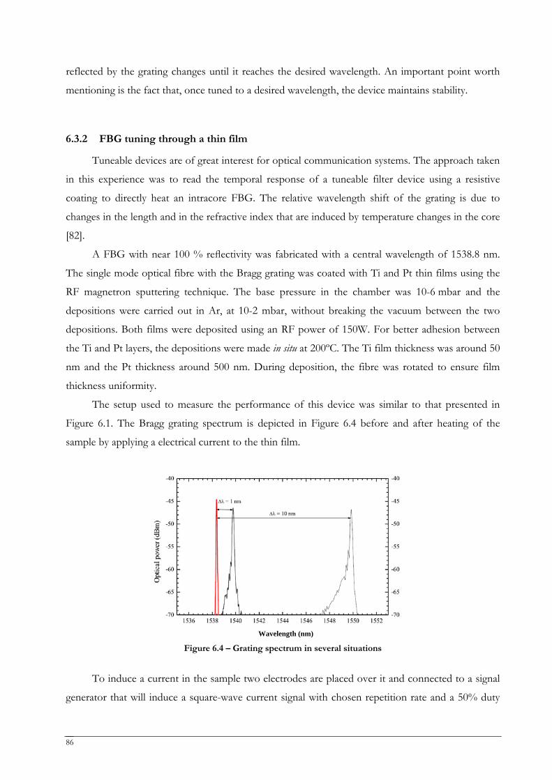
86
reflected by the grating changes until it reaches the desired wavelength. An important point worth
mentioning is the fact that, once tuned to a desired wavelength, the device maintains stability.
6.3.2 FBG tuning through a thin film
Tuneable devices are of great interest for optical communication systems. The approach taken
in this experience was to read the temporal response of a tuneable filter device using a resistive
coating to directly heat an intracore FBG. The relative wavelength shift of the grating is due to
changes in the length and in the refractive index that are induced by temperature changes in the core
[82].
A FBG with near 100 % reflectivity was fabricated with a central wavelength of 1538.8 nm.
The single mode optical fibre with the Bragg grating was coated with Ti and Pt thin films using the
RF magnetron sputtering technique. The base pressure in the chamber was 10-6 mbar and the
depositions were carried out in Ar, at 10-2 mbar, without breaking the vacuum between the two
depositions. Both films were deposited using an RF power of 150W. For better adhesion between
the Ti and Pt layers, the depositions were made in situ at 200ºC. The Ti film thickness was around 50
nm and the Pt thickness around 500 nm. During deposition, the fibre was rotated to ensure film
thickness uniformity.
The setup used to measure the performance of this device was similar to that presented in
Figure 6.1. The Bragg grating spectrum is depicted in Figure 6.4 before and after heating of the
sample by applying a electrical current to the thin film.
Wavelength (nm)
Figure 6.4 – Grating spectrum in several situations
To induce a current in the sample two electrodes are placed over it and connected to a signal
generator that will induce a square-wave current signal with chosen repetition rate and a 50% duty
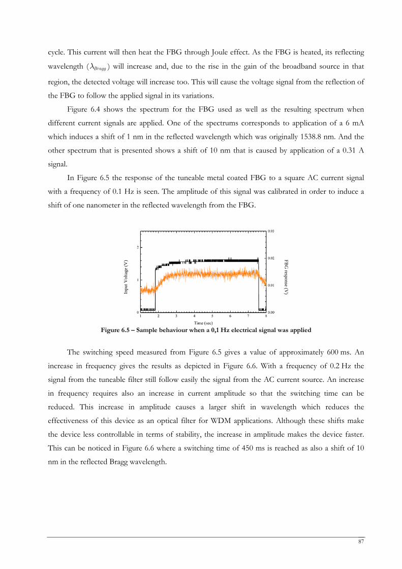
87
cycle. This current will then heat the FBG through Joule effect. As the FBG is heated, its reflecting
wavelength ( Braggλ ) will increase and, due to the rise in the gain of the broadband source in that
region, the detected voltage will increase too. This will cause the voltage signal from the reflection of
the FBG to follow the applied signal in its variations.
Figure 6.4 shows the spectrum for the FBG used as well as the resulting spectrum when
different current signals are applied. One of the spectrums corresponds to application of a 6 mA
which induces a shift of 1 nm in the reflected wavelength which was originally 1538.8 nm. And the
other spectrum that is presented shows a shift of 10 nm that is caused by application of a 0.31 A
signal.
In Figure 6.5 the response of the tuneable metal coated FBG to a square AC current signal
with a frequency of 0.1 Hz is seen. The amplitude of this signal was calibrated in order to induce a
shift of one nanometer in the reflected wavelength from the FBG.
Inpu
t Vol
tage
(V) FB
G response (V
)
Figure 6.5 – Sample behaviour when a 0,1 Hz electrical signal was applied
The switching speed measured from Figure 6.5 gives a value of approximately 600 ms. An
increase in frequency gives the results as depicted in Figure 6.6. With a frequency of 0.2 Hz the
signal from the tuneable filter still follow easily the signal from the AC current source. An increase
in frequency requires also an increase in current amplitude so that the switching time can be
reduced. This increase in amplitude causes a larger shift in wavelength which reduces the
effectiveness of this device as an optical filter for WDM applications. Although these shifts make
the device less controllable in terms of stability, the increase in amplitude makes the device faster.
This can be noticed in Figure 6.6 where a switching time of 450 ms is reached as also a shift of 10
nm in the reflected Bragg wavelength.
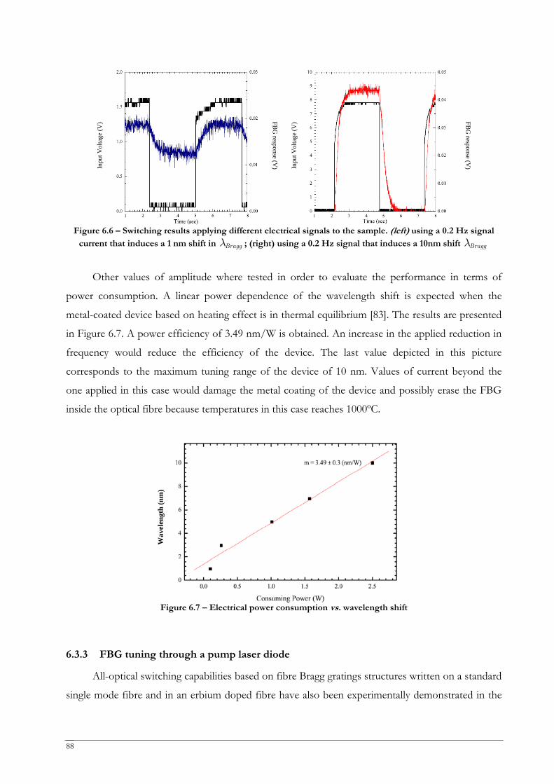
88
Inpu
t Vol
tage
(V)
FBG
response (V) In
put V
olta
ge (V
)
FBG
response (V)
Figure 6.6 – Switching results applying different electrical signals to the sample. (left) using a 0.2 Hz signal current that induces a 1 nm shift in Braggλ ; (right) using a 0.2 Hz signal that induces a 10nm shift Braggλ
Other values of amplitude where tested in order to evaluate the performance in terms of
power consumption. A linear power dependence of the wavelength shift is expected when the
metal-coated device based on heating effect is in thermal equilibrium [83]. The results are presented
in Figure 6.7. A power efficiency of 3.49 nm/W is obtained. An increase in the applied reduction in
frequency would reduce the efficiency of the device. The last value depicted in this picture
corresponds to the maximum tuning range of the device of 10 nm. Values of current beyond the
one applied in this case would damage the metal coating of the device and possibly erase the FBG
inside the optical fibre because temperatures in this case reaches 1000ºC.
W
avel
engt
h (n
m)
Figure 6.7 – Electrical power consumption vs. wavelength shift
6.3.3 FBG tuning through a pump laser diode
All-optical switching capabilities based on fibre Bragg gratings structures written on a standard
single mode fibre and in an erbium doped fibre have also been experimentally demonstrated in the
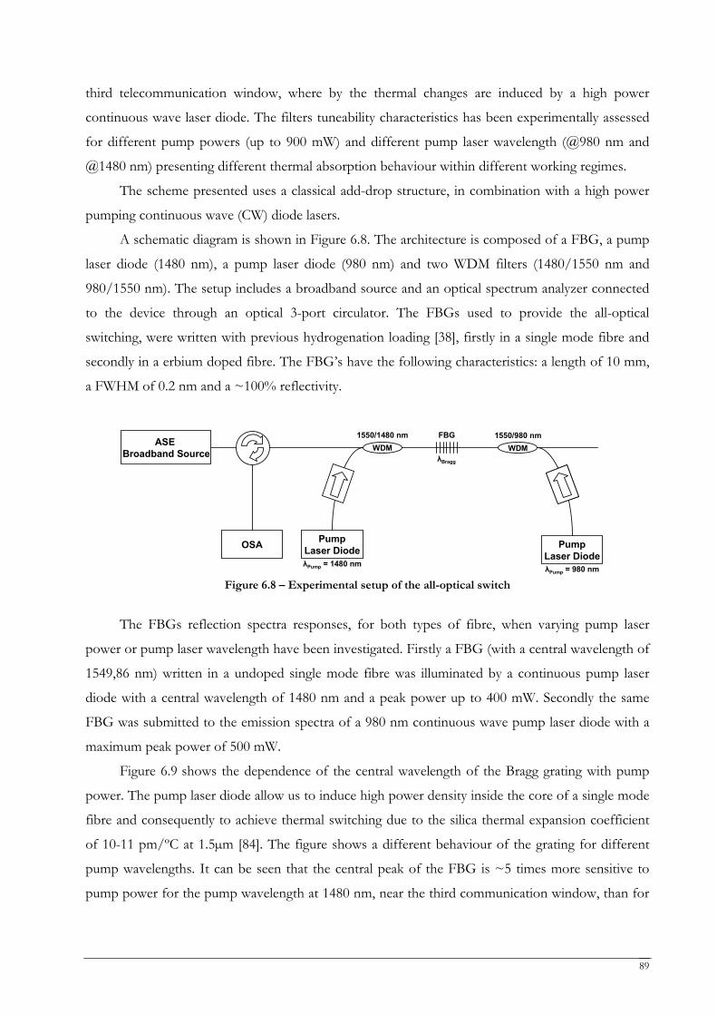
89
third telecommunication window, where by the thermal changes are induced by a high power
continuous wave laser diode. The filters tuneability characteristics has been experimentally assessed
for different pump powers (up to 900 mW) and different pump laser wavelength (@980 nm and
@1480 nm) presenting different thermal absorption behaviour within different working regimes.
The scheme presented uses a classical add-drop structure, in combination with a high power
pumping continuous wave (CW) diode lasers.
A schematic diagram is shown in Figure 6.8. The architecture is composed of a FBG, a pump
laser diode (1480 nm), a pump laser diode (980 nm) and two WDM filters (1480/1550 nm and
980/1550 nm). The setup includes a broadband source and an optical spectrum analyzer connected
to the device through an optical 3-port circulator. The FBGs used to provide the all-optical
switching, were written with previous hydrogenation loading [38], firstly in a single mode fibre and
secondly in a erbium doped fibre. The FBG’s have the following characteristics: a length of 10 mm,
a FWHM of 0.2 nm and a ~100% reflectivity.
WDM
PumpLaser Diode
1550/1480 nm FBG
λBragg
λPump = 1480 nm
WDM1550/980 nm
PumpLaser DiodeλPump = 980 nm
OSA
ASE Broadband Source
Figure 6.8 – Experimental setup of the all-optical switch
The FBGs reflection spectra responses, for both types of fibre, when varying pump laser
power or pump laser wavelength have been investigated. Firstly a FBG (with a central wavelength of
1549,86 nm) written in a undoped single mode fibre was illuminated by a continuous pump laser
diode with a central wavelength of 1480 nm and a peak power up to 400 mW. Secondly the same
FBG was submitted to the emission spectra of a 980 nm continuous wave pump laser diode with a
maximum peak power of 500 mW.
Figure 6.9 shows the dependence of the central wavelength of the Bragg grating with pump
power. The pump laser diode allow us to induce high power density inside the core of a single mode
fibre and consequently to achieve thermal switching due to the silica thermal expansion coefficient
of 10-11 pm/ºC at 1.5µm [84]. The figure shows a different behaviour of the grating for different
pump wavelengths. It can be seen that the central peak of the FBG is ~5 times more sensitive to
pump power for the pump wavelength at 1480 nm, near the third communication window, than for
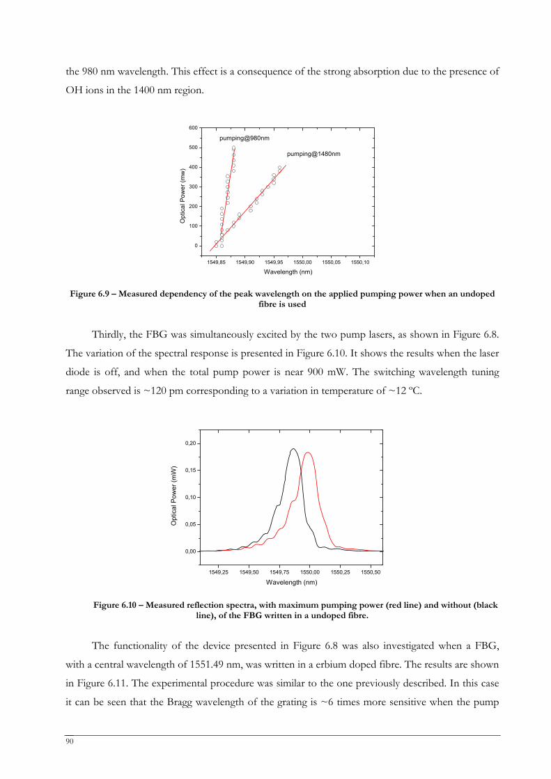
90
the 980 nm wavelength. This effect is a consequence of the strong absorption due to the presence of
OH ions in the 1400 nm region.
1549,85 1549,90 1549,95 1550,00 1550,05 1550,10
0
100
200
300
400
500
600
pumping@1480nm
pumping@980nm
Opt
ical
Pow
er (m
w)
Wavelength (nm)
Figure 6.9 – Measured dependency of the peak wavelength on the applied pumping power when an undoped
fibre is used
Thirdly, the FBG was simultaneously excited by the two pump lasers, as shown in Figure 6.8.
The variation of the spectral response is presented in Figure 6.10. It shows the results when the laser
diode is off, and when the total pump power is near 900 mW. The switching wavelength tuning
range observed is ~120 pm corresponding to a variation in temperature of ~12 ºC.
1549,25 1549,50 1549,75 1550,00 1550,25 1550,50
0,00
0,05
0,10
0,15
0,20
Opt
ical
Pow
er (m
W)
Wavelength (nm)
Figure 6.10 – Measured reflection spectra, with maximum pumping power (red line) and without (black
line), of the FBG written in a undoped fibre.
The functionality of the device presented in Figure 6.8 was also investigated when a FBG,
with a central wavelength of 1551.49 nm, was written in a erbium doped fibre. The results are shown
in Figure 6.11. The experimental procedure was similar to the one previously described. In this case
it can be seen that the Bragg wavelength of the grating is ~6 times more sensitive when the pump
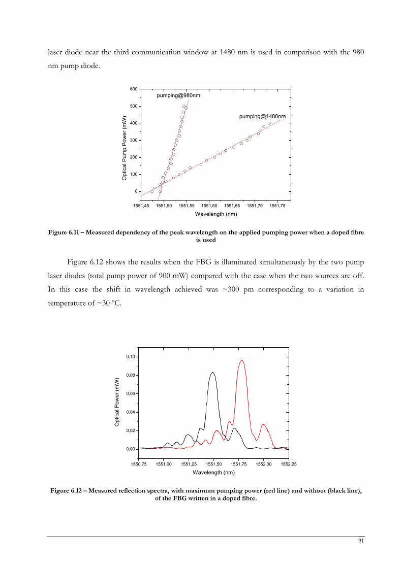
91
laser diode near the third communication window at 1480 nm is used in comparison with the 980
nm pump diode.
1551,45 1551,50 1551,55 1551,60 1551,65 1551,70 1551,75
0
100
200
300
400
500
600pumping@980nm
Opt
ical
Pum
p P
ower
(mW
)
Wavelength (nm)
pumping@1480nm
Figure 6.11 – Measured dependency of the peak wavelength on the applied pumping power when a doped fibre
is used
Figure 6.12 shows the results when the FBG is illuminated simultaneously by the two pump
laser diodes (total pump power of 900 mW) compared with the case when the two sources are off.
In this case the shift in wavelength achieved was ~300 pm corresponding to a variation in
temperature of ~30 ºC.
1550,75 1551,00 1551,25 1551,50 1551,75 1552,00 1552,25
0,00
0,02
0,04
0,06
0,08
0,10
Opt
ical
Pow
er (m
W)
Wavelength (nm)
Figure 6.12 – Measured reflection spectra, with maximum pumping power (red line) and without (black line),
of the FBG written in a doped fibre.
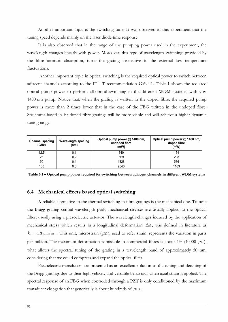
92
Another important topic is the switching time. It was observed in this experiment that the
tuning speed depends mainly on the laser diode time response.
It is also observed that in the range of the pumping power used in the experiment, the
wavelength changes linearly with power. Moreover, this type of wavelength switching, provided by
the fibre intrinsic absorption, turns the grating insensitive to the external low temperature
fluctuations.
Another important topic in optical switching is the required optical power to switch between
adjacent channels according to the ITU-T recommendation G.694.1. Table 1 shows the required
optical pump power to perform all-optical switching in the different WDM systems, with CW
1480 nm pump. Notice that, when the grating is written in the doped fibre, the required pump
power is more than 2 times lower that in the case of the FBG written in the undoped fibre.
Structures based in Er doped fibre gratings will be more viable and will achieve a higher dynamic
tuning range.
Channel spacing (GHz)
Wavelength spacing (nm)
Optical pump power @ 1480 nm, undoped fibre
(mW)
Optical pump power @ 1480 nm, doped fibre
(mW)
12.5 0.1 340 154 25 0.2 669 298 50 0.4 1328 586 100 0.8 2646 1163
Table 6.1 – Optical pump power required for switching between adjacent channels in different WDM systems
6.4 Mechanical effects based optical switching
A reliable alternative to the thermal switching in fibre gratings is the mechanical one. To tune
the Bragg grating central wavelength peak, mechanical stresses are usually applied to the optical
filter, usually using a piezoelectric actuator. The wavelength changes induced by the application of
mechanical stress which results in a longitudinal deformation εΔ , was defined in literature as
1, 3 pm/kε με= . This unit, microstrain (με ), used to refer strain, represents the variation in parts
per million. The maximum deformation admissible in commercial fibres is about 4% (40000 με ),
what allows the spectral tuning of the grating in a wavelength band of approximately 50 nm,
considering that we could compress and expand the optical filter.
Piezoelectric transducers are presented as an excellent solution to the tuning and detuning of
the Bragg gratings due to their high velocity and versatile behaviour when axial strain is applied. The
spectral response of an FBG when controlled through a PZT is only conditioned by the maximum
transducer elongation that generically is about hundreds of mμ .
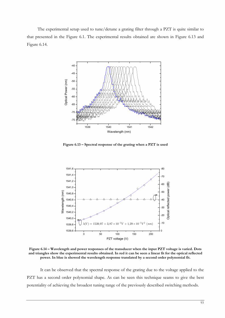
93
The experimental setup used to tune/detune a grating filter through a PZT is quite similar to
that presented in the Figure 6.1. The experimental results obtained are shown in Figure 6.13 and
Figure 6.14.
1539 1540 1541 1542
-75
-70
-65
-60
-55
-50
-45
-40
Opt
ical
Pow
er (n
m)
Wavelength (nm)
Figure 6.13 – Spectral response of the grating when a PZT is used
0 50 100 150 2001539,6
1539,8
1540,0
1540,2
1540,4
1540,6
1540,8
1541,0
1541,2
1541,4
1541,6
0
-10
-20
-30
-40
-50
-60
-70
-80O
ptic
al re
flect
ed p
ower
(dB)
Wav
elen
gth
(nm
)
PZT voltage (V)
3 5 2( ) 1539,97 3,87 10 1,29 10 ( )V V V nmλ − −= + × + ×
Figure 6.14 – Wavelength and power responses of the transducer when the input PZT voltage is varied. Dots and triangles show the experimental results obtained. In red it can be seen a linear fit for the optical reflected
power. In blue is showed the wavelength response translated by a second order polynomial fit.
It can be observed that the spectral response of the grating due to the voltage applied to the
PZT has a second order polynomial shape. As can be seen this technique seams to give the best
potentiality of achieving the broadest tuning range of the previously described switching methods.
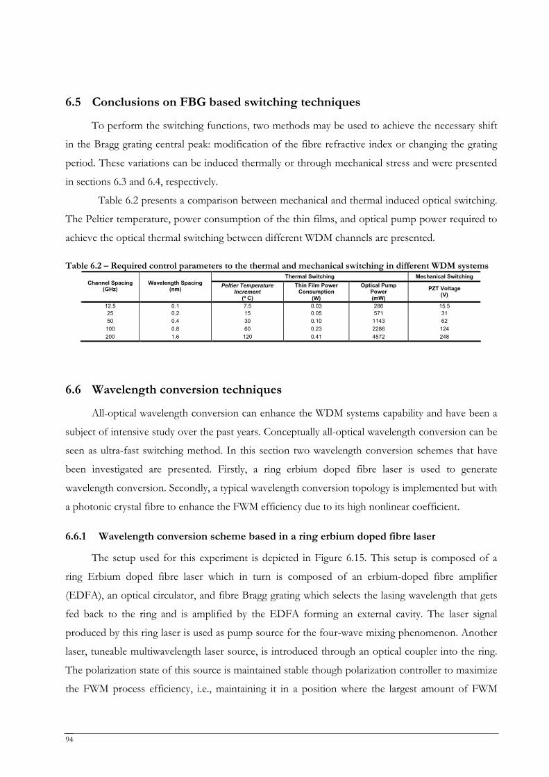
94
6.5 Conclusions on FBG based switching techniques
To perform the switching functions, two methods may be used to achieve the necessary shift
in the Bragg grating central peak: modification of the fibre refractive index or changing the grating
period. These variations can be induced thermally or through mechanical stress and were presented
in sections 6.3 and 6.4, respectively.
Table 6.2 presents a comparison between mechanical and thermal induced optical switching.
The Peltier temperature, power consumption of the thin films, and optical pump power required to
achieve the optical thermal switching between different WDM channels are presented. Table 6.2 – Required control parameters to the thermal and mechanical switching in different WDM systems
Thermal Switching Mechanical Switching Channel Spacing
(GHz) Wavelength Spacing
(nm) Peltier Temperature Increment
(º C)
Thin Film Power Consumption
(W)
Optical Pump Power (mW)
PZT Voltage (V)
12.5 0.1 7.5 0.03 286 15.5 25 0.2 15 0.05 571 31 50 0.4 30 0.10 1143 62
100 0.8 60 0.23 2286 124 200 1.6 120 0.41 4572 248
6.6 Wavelength conversion techniques
All-optical wavelength conversion can enhance the WDM systems capability and have been a
subject of intensive study over the past years. Conceptually all-optical wavelength conversion can be
seen as ultra-fast switching method. In this section two wavelength conversion schemes that have
been investigated are presented. Firstly, a ring erbium doped fibre laser is used to generate
wavelength conversion. Secondly, a typical wavelength conversion topology is implemented but with
a photonic crystal fibre to enhance the FWM efficiency due to its high nonlinear coefficient.
6.6.1 Wavelength conversion scheme based in a ring erbium doped fibre laser
The setup used for this experiment is depicted in Figure 6.15. This setup is composed of a
ring Erbium doped fibre laser which in turn is composed of an erbium-doped fibre amplifier
(EDFA), an optical circulator, and fibre Bragg grating which selects the lasing wavelength that gets
fed back to the ring and is amplified by the EDFA forming an external cavity. The laser signal
produced by this ring laser is used as pump source for the four-wave mixing phenomenon. Another
laser, tuneable multiwavelength laser source, is introduced through an optical coupler into the ring.
The polarization state of this source is maintained stable though polarization controller to maximize
the FWM process efficiency, i.e., maintaining it in a position where the largest amount of FWM
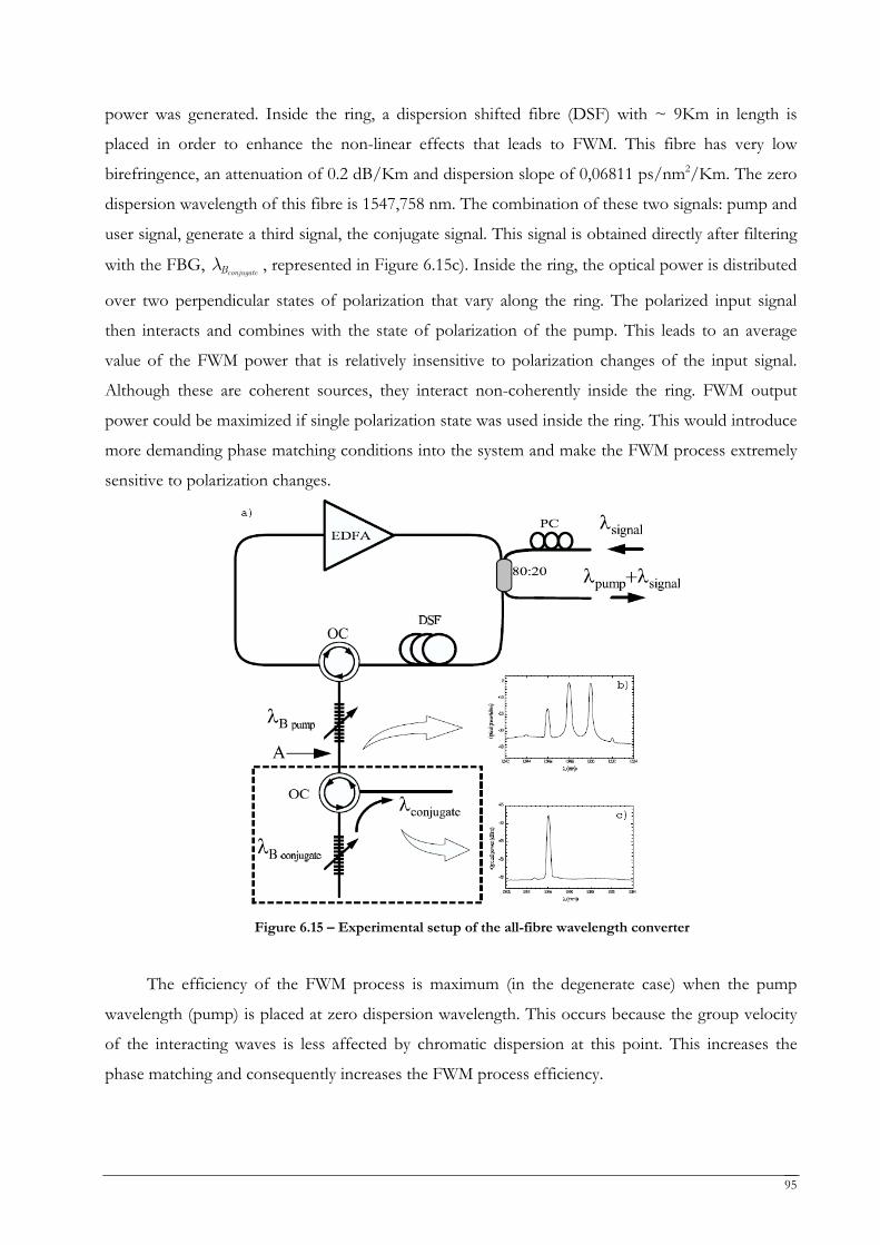
95
power was generated. Inside the ring, a dispersion shifted fibre (DSF) with ~ 9Km in length is
placed in order to enhance the non-linear effects that leads to FWM. This fibre has very low
birefringence, an attenuation of 0.2 dB/Km and dispersion slope of 0,06811 ps/nm2/Km. The zero
dispersion wavelength of this fibre is 1547,758 nm. The combination of these two signals: pump and
user signal, generate a third signal, the conjugate signal. This signal is obtained directly after filtering
with the FBG, conjugateBλ , represented in Figure 6.15c). Inside the ring, the optical power is distributed
over two perpendicular states of polarization that vary along the ring. The polarized input signal
then interacts and combines with the state of polarization of the pump. This leads to an average
value of the FWM power that is relatively insensitive to polarization changes of the input signal.
Although these are coherent sources, they interact non-coherently inside the ring. FWM output
power could be maximized if single polarization state was used inside the ring. This would introduce
more demanding phase matching conditions into the system and make the FWM process extremely
sensitive to polarization changes.
Figure 6.15 – Experimental setup of the all-fibre wavelength converter
The efficiency of the FWM process is maximum (in the degenerate case) when the pump
wavelength (pump) is placed at zero dispersion wavelength. This occurs because the group velocity
of the interacting waves is less affected by chromatic dispersion at this point. This increases the
phase matching and consequently increases the FWM process efficiency.
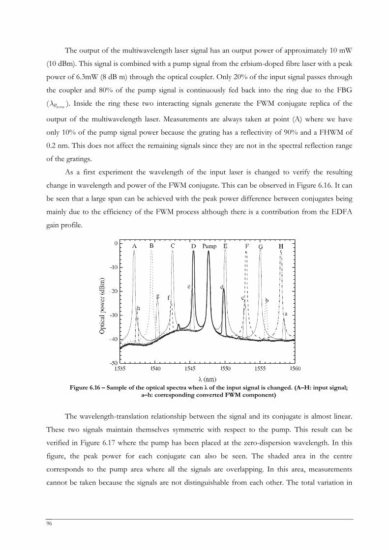
96
The output of the multiwavelength laser signal has an output power of approximately 10 mW
(10 dBm). This signal is combined with a pump signal from the erbium-doped fibre laser with a peak
power of 6.3mW (8 dB m) through the optical coupler. Only 20% of the input signal passes through
the coupler and 80% of the pump signal is continuously fed back into the ring due to the FBG
(pumpBλ ). Inside the ring these two interacting signals generate the FWM conjugate replica of the
output of the multiwavelength laser. Measurements are always taken at point (A) where we have
only 10% of the pump signal power because the grating has a reflectivity of 90% and a FHWM of
0.2 nm. This does not affect the remaining signals since they are not in the spectral reflection range
of the gratings.
As a first experiment the wavelength of the input laser is changed to verify the resulting
change in wavelength and power of the FWM conjugate. This can be observed in Figure 6.16. It can
be seen that a large span can be achieved with the peak power difference between conjugates being
mainly due to the efficiency of the FWM process although there is a contribution from the EDFA
gain profile.
Figure 6.16 – Sample of the optical spectra when λ of the input signal is changed. (A–H: input signal;
a–h: corresponding converted FWM component)
The wavelength-translation relationship between the signal and its conjugate is almost linear.
These two signals maintain themselves symmetric with respect to the pump. This result can be
verified in Figure 6.17 where the pump has been placed at the zero-dispersion wavelength. In this
figure, the peak power for each conjugate can also be seen. The shaded area in the centre
corresponds to the pump area where all the signals are overlapping. In this area, measurements
cannot be taken because the signals are not distinguishable from each other. The total variation in
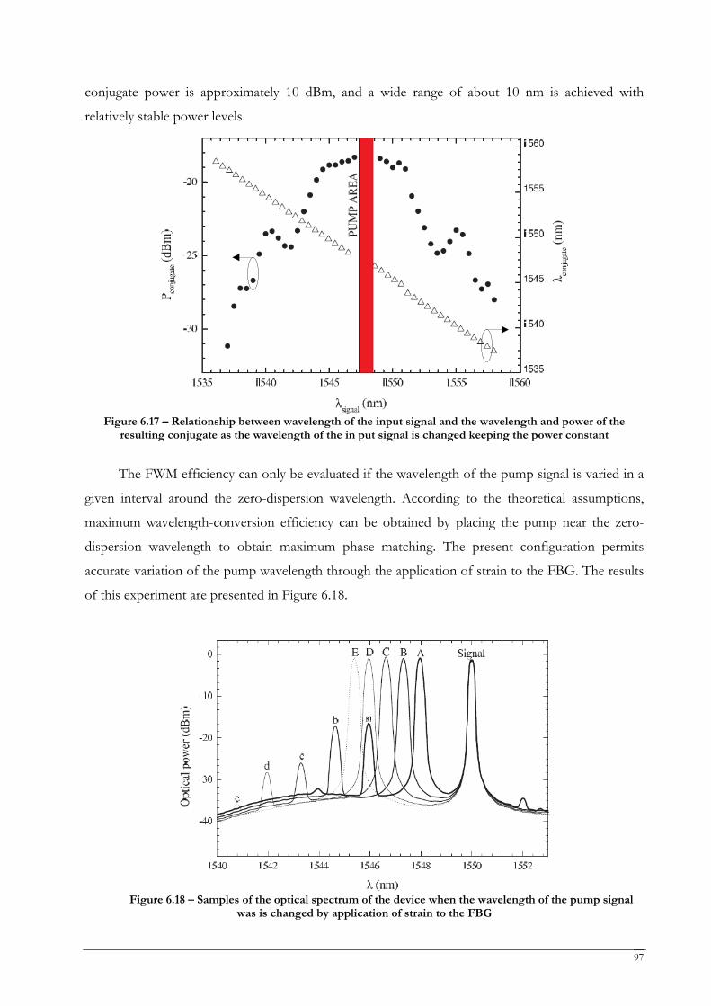
97
conjugate power is approximately 10 dBm, and a wide range of about 10 nm is achieved with
relatively stable power levels.
Figure 6.17 – Relationship between wavelength of the input signal and the wavelength and power of the
resulting conjugate as the wavelength of the in put signal is changed keeping the power constant
The FWM efficiency can only be evaluated if the wavelength of the pump signal is varied in a
given interval around the zero-dispersion wavelength. According to the theoretical assumptions,
maximum wavelength-conversion efficiency can be obtained by placing the pump near the zero-
dispersion wavelength to obtain maximum phase matching. The present configuration permits
accurate variation of the pump wavelength through the application of strain to the FBG. The results
of this experiment are presented in Figure 6.18.
Figure 6.18 – Samples of the optical spectrum of the device when the wavelength of the pump signal
was is changed by application of strain to the FBG
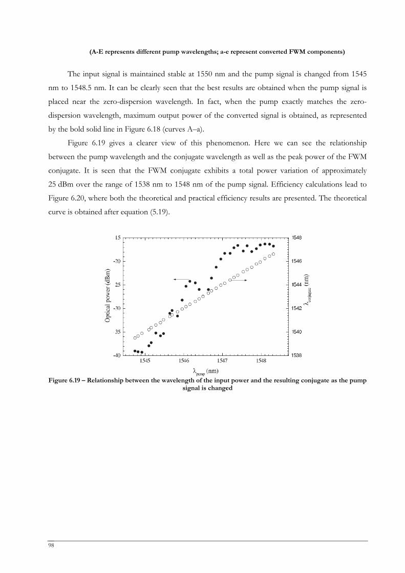
98
(A-E represents different pump wavelengths; a-e represent converted FWM components)
The input signal is maintained stable at 1550 nm and the pump signal is changed from 1545
nm to 1548.5 nm. It can be clearly seen that the best results are obtained when the pump signal is
placed near the zero-dispersion wavelength. In fact, when the pump exactly matches the zero-
dispersion wavelength, maximum output power of the converted signal is obtained, as represented
by the bold solid line in Figure 6.18 (curves A–a).
Figure 6.19 gives a clearer view of this phenomenon. Here we can see the relationship
between the pump wavelength and the conjugate wavelength as well as the peak power of the FWM
conjugate. It is seen that the FWM conjugate exhibits a total power variation of approximately
25 dBm over the range of 1538 nm to 1548 nm of the pump signal. Efficiency calculations lead to
Figure 6.20, where both the theoretical and practical efficiency results are presented. The theoretical
curve is obtained after equation (5.19).
Figure 6.19 – Relationship between the wavelength of the input power and the resulting conjugate as the pump
signal is changed
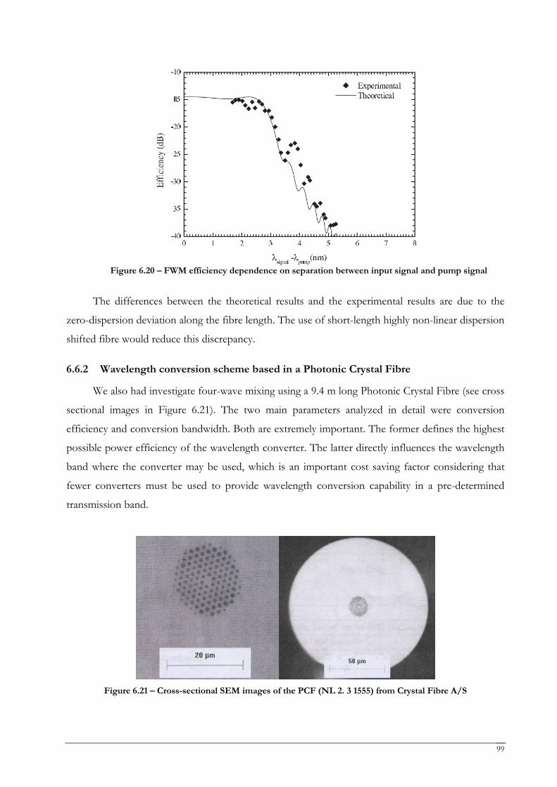
99
Figure 6.20 – FWM efficiency dependence on separation between input signal and pump signal
The differences between the theoretical results and the experimental results are due to the
zero-dispersion deviation along the fibre length. The use of short-length highly non-linear dispersion
shifted fibre would reduce this discrepancy.
6.6.2 Wavelength conversion scheme based in a Photonic Crystal Fibre
We also had investigate four-wave mixing using a 9.4 m long Photonic Crystal Fibre (see cross
sectional images in Figure 6.21). The two main parameters analyzed in detail were conversion
efficiency and conversion bandwidth. Both are extremely important. The former defines the highest
possible power efficiency of the wavelength converter. The latter directly influences the wavelength
band where the converter may be used, which is an important cost saving factor considering that
fewer converters must be used to provide wavelength conversion capability in a pre-determined
transmission band.
Figure 6.21 – Cross-sectional SEM images of the PCF (NL 2. 3 1555) from Crystal Fibre A/S
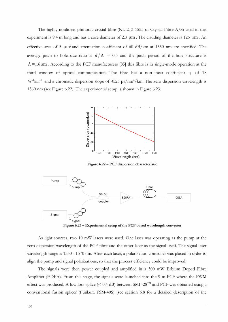
100
The highly nonlinear photonic crystal fibre (NL 2. 3 1555 of Crystal Fibre A/S) used in this
experiment is 9.4 m long and has a core diameter of 2.3 mμ . The cladding diameter is 125 mμ . An
effective area of 5 2mμ and attenuation coefficient of 60 dB/km at 1550 nm are specified. The
average pitch to hole size ratio is /d Λ = 0.5 and the pitch period of the hole structure is
Λ=1.6 mμ . According to the PCF manufacturers [85] this fibre is in single-mode operation at the
third window of optical communication. The fibre has a non-linear coefficient γ of 18 -1 -1W km and a chromatic dispersion slope of -0.25 ps/nm2/km. The zero dispersion wavelength is
1560 nm (see Figure 6.22). The experimental setup is shown in Figure 6.23.
Figure 6.22 – PCF dispersion characteristic
Signal
λ Fibre
OSA
Pump
λsignal
pump
EDFA50:50
coupler
Figure 6.23 – Experimental setup of the PCF based wavelength converter
As light sources, two 10 mW lasers were used. One laser was operating as the pump at the
zero dispersion wavelength of the PCF fibre and the other laser as the signal itself. The signal laser
wavelength range is 1530 - 1570 nm. After each laser, a polarization controller was placed in order to
align the pump and signal polarizations, so that the process efficiency could be improved.
The signals were then power coupled and amplified in a 500 mW Erbium Doped Fibre
Amplifier (EDFA). From this stage, the signals were launched into the 9 m PCF where the FWM
effect was produced. A low loss splice (< 0.4 dB) between SMF-28TM and PCF was obtained using a
conventional fusion splicer (Fujikura FSM-40S) (see section 6.8 for a detailed description of the
101
splicing method developed). At the other end, wavelength generation as a result of the FWM was
monitored using an Optical Spectrum Analyzer (OSA). The result is shown in Figure 6.24
1540 1550 1560 1570
-30
0
30
Satellite Converted
Signal
Opt
ical
pow
er (d
Bm
)
Wavelength (nm)
Pump
Figure 6.24 – Measured spectra for different input signals
This figure shows the measured spectra of the pump, satellite and converted signals, the
arrows indicating the evolution of the signals with the progression of the input signal through the
ITU WDM grid. Figure 6.25 shows the measured conversion efficiency. Measurements were taken
over the range of 16 nm centred on 1560 nm.
0 2 4 6 8 10 12 14 16 18-110
-100
-90
-80
-70
-60
-50
-40
-30
-20
-10
Effic
ienc
y (d
B)
λpump-λsignal (nm)
Theoretical efficency Measured efficiency
Figure 6.25 – Four wave mixing conversion efficiency
A conversion efficiency of approximately -35 dB was obtained, over a bandwidth of 10 nm
(20 nm two-sided bandwidth). The dashed line in Figure 6.25 shows the corresponding theoretical
102
results obtained from equation (5.19). These are in good agreement with the experimental results.
When compared with previously published results, our experiment demonstrates broader
bandwidth, albeit a lower efficiency. Despite having higher dispersion slope, the fact that the PCF
length is small is the reason for the relatively large bandwidth obtained. The high value for the
attenuation, α, originates an effective length, effL of 8.8 m, which limits the maximum available
conversion efficiency.
6.7 Conclusions on wavelength conversion schemes
An all fibre wavelength converter based on four-wave mixing in a ring erbium doped fibre
laser have been demonstrated in section 6.6.1 (and the main result of this work have been patented –
see Appendix 1). Degenerate FWM near the zero dispersion wavelength region was studied. The
experimental results are in good agreement with theory. Performance levels are limited by the type
of fibre used (DSF), which does not have a sufficiently high nonlinear coefficient to ensure good
degenerate FWM process efficiency levels. Nonetheless, the results compare favourably with
previous published results. This structure is also very resistant to changes in the polarization state of
the interacting signals. We are pursuing all-fibre FWM wavelength conversion because of the
feasible advantage of its transparency; the conversion can be insensitive to the modulation bit rate
and format, in contrast to grating-type wavelength conversion.
Wavelength conversion through the FWM effect has also been achieved using a PCF with a
high non-linear coefficient. A theoretical and experimental study of the conversion efficiency and
operation bandwidth has been presented in section 6.6.2. A conversion efficiency of -35 dB over a
bandwidth of 20 nm has been obtained in good agreement with the theoretical results. A great
advantage of the PCF is the small length of fibre required to achieve wavelength conversion due to
its high non-linear coefficient. One other main advantage of this kind of fibres is its broader
bandwidth in comparison to other fibres where FWM can be obtained, such as DSF. In conclusion,
PCF is more suitable for applications requiring broader bandwidths, such as dense WDM.
Moreover, wavelength converters using PCF can be made much smaller, which can be a very
important reason to develop PCF-based wavelength converters or routers. Work is also under way
to develop optical switches/cross-connects based on non-linear effects in photonic crystal fibres.
6.8 Splicing PCFs with SMFs for wavelength conversion purposes
An important issue in the practical applications of photonic crystal fibres (PCF) is its
connection with single mode fibres (SMF) with low loss. Good splicing of photonic crystal fibres to
103
standard SMF is extremely vital in order to enhance its potential use in communication systems.
Furthermore, splicing of fibres with different glass materials is difficult due to the different
coefficients of thermal expansion and melting temperatures of the two fibres.
In 1999, Bennett [86] reported a splice loss of 1.5 dB using a conventional fusion splicer
between a holey fibre and a SMF-28TM (Corning). An alternative method has been proposed in 2003
by Chong [87] using a CO2 Laser and a splice loss in the range of 1.3-2.8 dB was obtained. This
technique is used in order to avoid hole collapsing and the condensation trapping inside the PCF
during the splicing process.
Also in 2003, Bourliaguet [88] described a simple method that can be used to splice photonic
crystal fibres relying only on commercial electric-arc splicers [89, 90]. The results were presented in
terms of fusion losses [85] and tensile strength. A range of 0.6 and 0.9 dB fusion losses were
obtained for 0.40 or 0.45 second arc durations.
A simple method to fuse a PCF with an SMF-28TM achieving, to the best of our knowledge,
the lowest splice loss reported to date with these fibres. Measurements are reported for the splice
loss as a function of arc duration and current discharge. Optimisation of these parameters means the
splice can be performed easily with high reproductibility. In our experiments the Fujikura’s FSM-
40S fusion splicer was used.
6.8.1 Experimental results
The splice technique reported relies on butting the fibres, the electric arc discharge being
applied over the SMF region. This required the electric arc fusion splicer to be operated in manual
mode to control the region of the SMF-28TM (core diameter and numerical aperture are respectively
8.2 μm and 0.4) where the electric arc should be applied. During the splicing process the results for
the loss were obtained, using the well known cutback technique, by injecting light into the SMF-28TM
from a tuneable laser source (TL200C from Thorlabs, Inc.) operating with wavelength peak of 1550
nm. The procedure is now described. First the fibres were automatically joined to a distance of
25 μm of each other (the region where the arc usually discharge) as seen in Figure 6.26a). From this
moment on all the fusion process was manually operated. The PCF position was kept fixed and then
the SMF-28TM was moved against the PCF, using the translation stage of the machine. The two
fibres were butted and aligned the fibre losses of this alignment quantified. After optimization of the
alignment a minimum loss of 5 dB was measured. This 5 dB value was achieved when both fibres
were aligned without any matching.
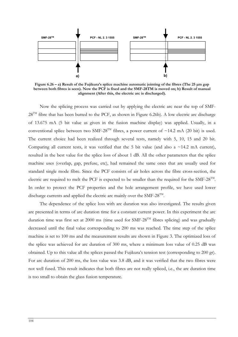
104
a) b)
SMF-28TM PCF - NL 2. 3 1555 SMF-28TM PCF - NL 2. 3 1555
Figure 6.26 – a) Result of the Fujikura’s splice machine automatic jointing of the fibres (The 25 μm gap
between both fibres is seen). Now the PCF is fixed and the SMF-28TM is moved on; b) Result of manual alignment (After this, the electric arc is discharged).
Now the splicing process was carried out by applying the electric arc near the top of SMF-
28TM fibre that has been butted to the PCF, as shown in Figure 6.26b). A low electric arc discharge
of 13.675 mA (5 bit value as given in the fusion machine display) was applied. Usually, in a
conventional splice between two SMF-28TM fibres, a power current of ~14.2 mA (20 bit) is used.
The current choice had been realized through several tests, namely with 5, 10, 15 and 20 bit.
Comparing all current tests, it was verified that the 5 bit value (and also a ~14.2 mA current),
resulted in the best value for the splice loss of about 1 dB. All the other parameters that the splice
machine uses (overlap, gap, prefuse, etc), had remained the same ones that are usually used for
standard single mode fibre. Since the PCF consists of air holes across the fibre cross-section, the
electric arc required to melt the PCF is expected to be smaller than the required for the SMF-28TM.
In order to protect the PCF properties and the hole arrangement profile, we have used lower
discharge currents and applied the electric arc mainly over the SMF-28TM.
The dependence of the splice loss with arc duration was also investigated. The results given
are presented in terms of arc duration time for a constant current power. In this experiment the arc
duration time was first set at 2000 ms (time used for SMF-28TM fibres splicing) and was gradually
decreased until the final value corresponding to 200 ms was reached. The time step of the splice
machine is set to 100 ms and the measurement results are shown in Figure 3. The optimized loss of
the splice was achieved for arc duration of 300 ms, where a minimum loss value of 0.25 dB was
obtained. Up to this value all the splices passed the Fujikura’s tension test (corresponding to 200 gr).
For arc duration of 200 ms, the loss value was 3.8 dB, and it was verified that the two fibres were
not well fused. This result indicates that both fibres are not really spliced, i.e., the arc duration time
is too small to obtain the glass fusion temperature.
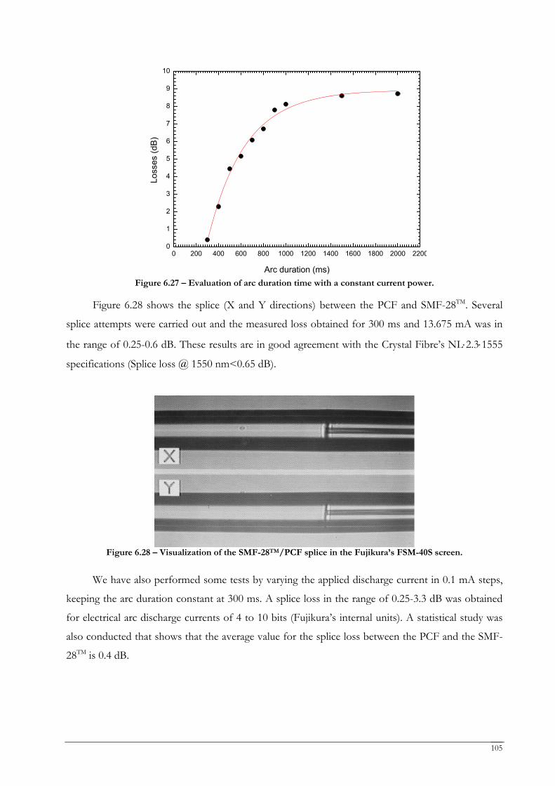
105
0 200 400 600 800 1000 1200 1400 1600 1800 2000 22000
1
2
3
4
5
6
7
8
9
10
Loss
es (d
B)
Arc duration (ms) Figure 6.27 – Evaluation of arc duration time with a constant current power.
Figure 6.28 shows the splice (X and Y directions) between the PCF and SMF-28TM. Several
splice attempts were carried out and the measured loss obtained for 300 ms and 13.675 mA was in
the range of 0.25-0.6 dB. These results are in good agreement with the Crystal Fibre’s NL⋅2.3⋅1555
specifications (Splice loss @ 1550 nm<0.65 dB).
Figure 6.28 – Visualization of the SMF-28TM/PCF splice in the Fujikura’s FSM-40S screen.
We have also performed some tests by varying the applied discharge current in 0.1 mA steps,
keeping the arc duration constant at 300 ms. A splice loss in the range of 0.25-3.3 dB was obtained
for electrical arc discharge currents of 4 to 10 bits (Fujikura’s internal units). A statistical study was
also conducted that shows that the average value for the splice loss between the PCF and the SMF-
28TM is 0.4 dB.
106
6.8.2 Conclusions on splicing issues
The development of systems based on PCFs can not be viewed as an insuperable barrier due
to the fusion splice losses between these fibres and the standard ones. The results reported suggest
that the SMF-28TM/PCF fusion is capable of being done with very good results and high
reproducibility. The obtained results are within the range of 0.25-0.6 dB for 300 ms arc duration and
13.675 mA current discharge. In spite of being very challenging, the splicing process could easily be
achieved using standard fusion splicers. A technique was presented whereby a low loss splice was
achieved by applying an electric arc discharge mainly on the SMF-28TM region. This avoids the
collapsing of the air holes in the PCF, caused by the different melting point temperatures along the
transversal direction of the PCF structure. Using this technique was demonstrated that a low splice
loss can be achieved.
6.9 Summary
Optical switching is capable of being done using different techniques. In this chapter several
solutions were purposed to achieve optical switching with fibre Bragg gratings. It was demonstrated
that the FBG thermal switching can be obtained with Peltier elements, thin film deposition and
pump laser diode schemes. Mechanical strain can also be used to induce wavelength changes in
FBGs and a PZT is a faster solution than the ones based on thermal effects.
Finally nonlinear based wavelength conversion relying in the FWM effect was present as an
ultra-fast optical switching method. Experiments using dispersion shifted and photonic crystal fibres
were carried out and at last an extended description on splicing a PCF and SMF for optical
switching purposes was presented.
7 Development of optical network elements
7.1 Introduction
Multiwavelength optical add-drop multiplexers (OADM) and optical cross-connects (OXC),
will play a key role in providing more reconfiguration flexibility and network survivability in
wavelength division multiplexing (WDM) transport networks. Several architectures for OADMs and
OXCs using fibre Bragg gratings (FBGs) have been proposed.
In section 7.2 the performance of an OADM based in an apodized fibre Bragg Grating and
optical circulators at 10 Gb/s is tested and its performance evaluated in terms of crosstalk and bit
error rate (BER) measurements.
It is also proposed and demonstrated, in section 7.3, an architecture of a 2×2 OXC using
tuneable fibre Bragg gratings and optical circulators. This OXC is scalable to N×N ports owing to
the cascadability of individual routing modules, which perform routing of specific wavelength
channels. The performance of the cross-connect is also experimentally evaluated.
7.2 Optical add-drop multiplexers
Optical Add Drop Multiplexers (OADMs) are key components in optical switching networks.
Many types of these devices have been demonstrated but the structures based in Fibre Bragg
Gratings (FBGs) and Optical Circulators (OCs) are the most attractive because of their low cost,
low insertion losses, low crosstalk, precise wavelength selectivity, and due to the fact they don’t need
power supply.
7.2.1 Experimental implementation of an OADM
An OADM was developed using a apodized FBG (AFBG), with a Bragg wavelength of
1542.75 nm, a FWHM of 0.18 nm and ~90% of reflectivity. The transmission and reflection spectral
responses of the AFBG can be seen in Figure 7.1.
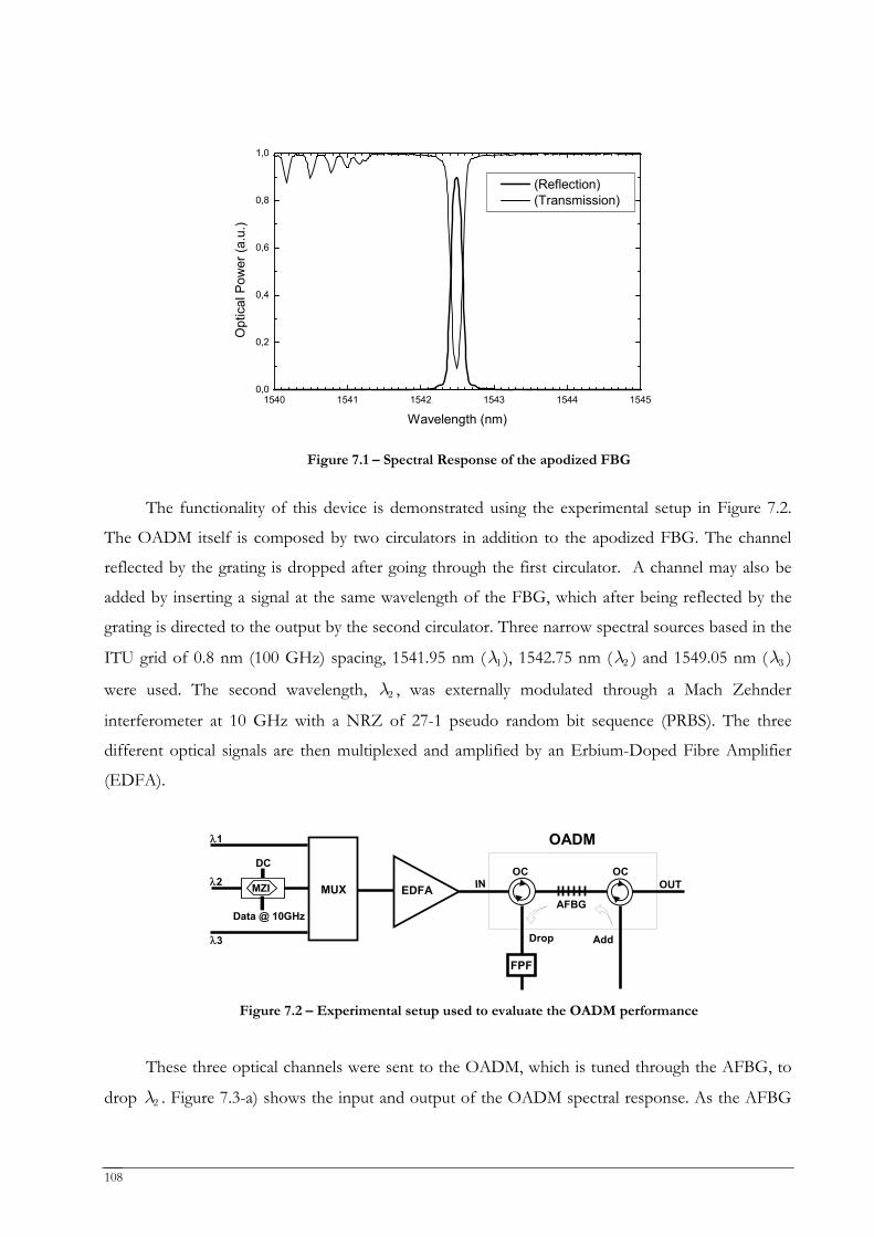
108
1540 1541 1542 1543 1544 15450,0
0,2
0,4
0,6
0,8
1,0
(Reflection) (Transmission)
Opt
ical
Pow
er (a
.u.)
Wavelength (nm)
Figure 7.1 – Spectral Response of the apodized FBG
The functionality of this device is demonstrated using the experimental setup in Figure 7.2.
The OADM itself is composed by two circulators in addition to the apodized FBG. The channel
reflected by the grating is dropped after going through the first circulator. A channel may also be
added by inserting a signal at the same wavelength of the FBG, which after being reflected by the
grating is directed to the output by the second circulator. Three narrow spectral sources based in the
ITU grid of 0.8 nm (100 GHz) spacing, 1541.95 nm ( 1λ ), 1542.75 nm ( 2λ ) and 1549.05 nm ( 3λ )
were used. The second wavelength, 2λ , was externally modulated through a Mach Zehnder
interferometer at 10 GHz with a NRZ of 27-1 pseudo random bit sequence (PRBS). The three
different optical signals are then multiplexed and amplified by an Erbium-Doped Fibre Amplifier
(EDFA).
DC
MZI
Data @ 10GHz
OC
AFBG
Drop
INOC
OUT
Add
OADM
λ2MUX
λ1
λ3
EDFA
FPF
Figure 7.2 – Experimental setup used to evaluate the OADM performance
These three optical channels were sent to the OADM, which is tuned through the AFBG, to
drop 2λ . Figure 7.3-a) shows the input and output of the OADM spectral response. As the AFBG
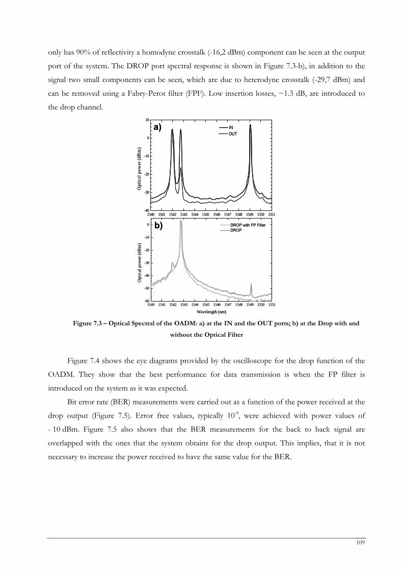
109
only has 90% of reflectivity a homodyne crosstalk (-16,2 dBm) component can be seen at the output
port of the system. The DROP port spectral response is shown in Figure 7.3-b), in addition to the
signal two small components can be seen, which are due to heterodyne crosstalk (-29,7 dBm) and
can be removed using a Fabry-Perot filter (FPF). Low insertion losses, ~1.3 dB, are introduced to
the drop channel.
1540 1541 1542 1543 1544 1545 1546 1547 1548 1549 1550 1551-40
-30
-20
-10
0
10
-40
-30
-20
-10
0
10 IN
Opt
ical
pow
er (d
Bm
) OUT
1540 1541 1542 1543 1544 1545 1546 1547 1548 1549 1550 1551-60
-50
-40
-30
-20
-10
0
-60
-50
-40
-30
-20
-10
0
Opt
ical
pow
er (d
Bm
)
Wavelength (nm)
DROP with FP Filter DROP
a)
b)1540 1541 1542 1543 1544 1545 1546 1547 1548 1549 1550 1551
-40
-30
-20
-10
0
10
-40
-30
-20
-10
0
10 IN
Opt
ical
pow
er (d
Bm
) OUT
1540 1541 1542 1543 1544 1545 1546 1547 1548 1549 1550 1551-60
-50
-40
-30
-20
-10
0
-60
-50
-40
-30
-20
-10
0
Opt
ical
pow
er (d
Bm
)
Wavelength (nm)
DROP with FP Filter DROP
a)
b)
Figure 7.3 – Optical Spectral of the OADM: a) at the IN and the OUT ports; b) at the Drop with and
without the Optical Filter
Figure 7.4 shows the eye diagrams provided by the oscilloscope for the drop function of the
OADM. They show that the best performance for data transmission is when the FP filter is
introduced on the system as it was expected.
Bit error rate (BER) measurements were carried out as a function of the power received at the
drop output (Figure 7.5). Error free values, typically 10-9, were achieved with power values of
- 10 dBm. Figure 7.5 also shows that the BER measurements for the back to back signal are
overlapped with the ones that the system obtains for the drop output. This implies, that it is not
necessary to increase the power received to have the same value for the BER.
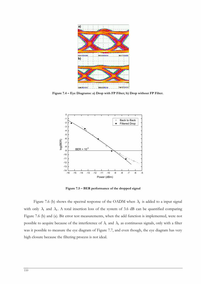
110
a)
b)
a)
b)
Figure 7.4 – Eye Diagrams: a) Drop with FP Filter; b) Drop without FP Filter.
-16 -15 -14 -13 -12 -11 -10 -9 -8 -7 -6 -5-14
-13
-12
-11
-10
-9
-8
-7
-6
-5
-4
-3
-2
-1
0
Back to Back Filtered Drop
BER = 10-9
log(
BE
R)
Power (dBm)
Figure 7.5 – BER performance of the dropped signal
Figure 7.6 (b) shows the spectral response of the OADM when 2λ is added to a input signal
with only 1λ and 3λ . A total insertion loss of the system of 3.6 dB can be quantified comparing
Figure 7.6 (b) and (a). Bit error test measurements, when the add function is implemented, were not
possible to acquire because of the interference of 1λ and 3λ as continuous signals, only with a filter
was it possible to measure the eye diagram of Figure 7.7, and even though, the eye diagram has very
high closure because the filtering process is not ideal.
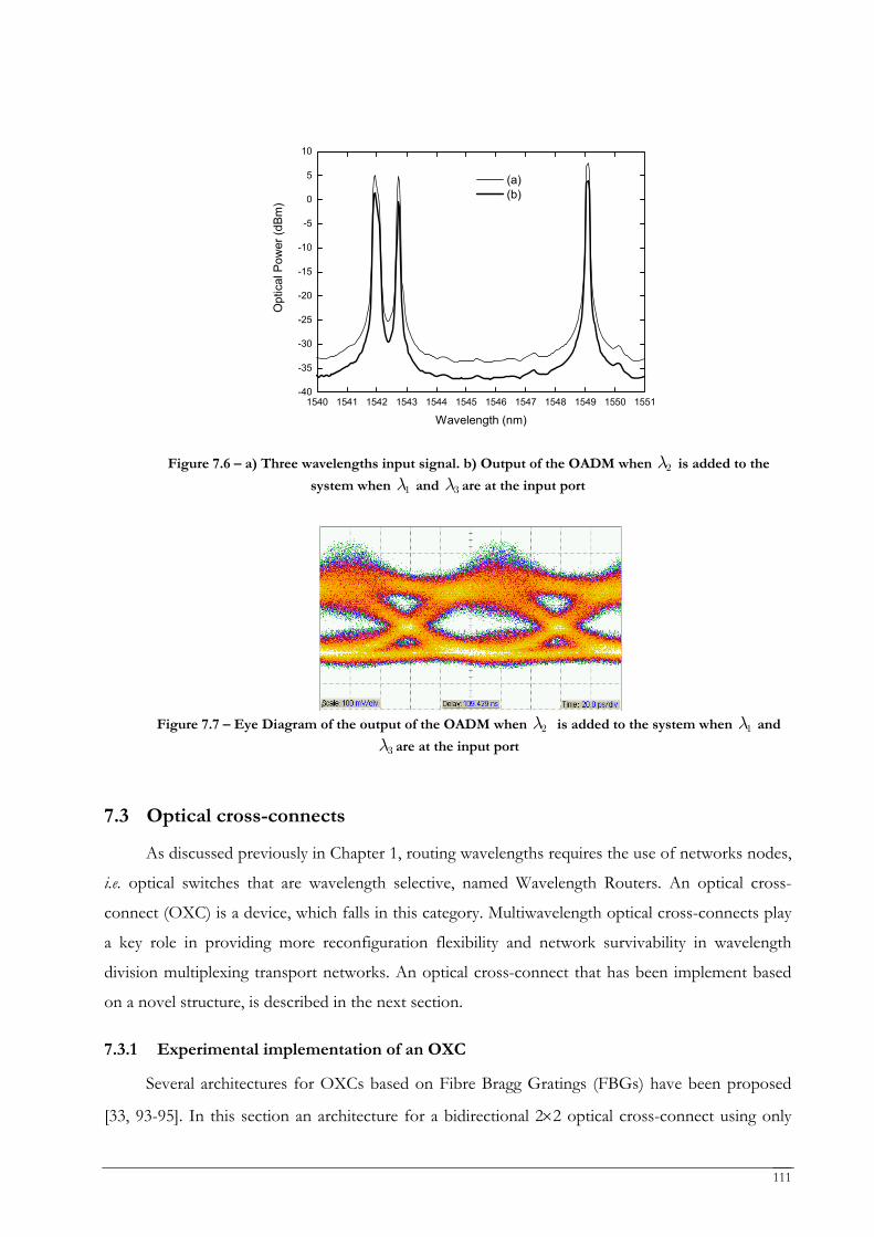
111
1540 1541 1542 1543 1544 1545 1546 1547 1548 1549 1550 1551-40
-35
-30
-25
-20
-15
-10
-5
0
5
10
(a) (b)
Opt
ical
Pow
er (d
Bm)
Wavelength (nm)
Figure 7.6 – a) Three wavelengths input signal. b) Output of the OADM when 2λ is added to the
system when 1λ and 3λ are at the input port
Figure 7.7 – Eye Diagram of the output of the OADM when 2λ is added to the system when 1λ and
3λ are at the input port
7.3 Optical cross-connects
As discussed previously in Chapter 1, routing wavelengths requires the use of networks nodes,
i.e. optical switches that are wavelength selective, named Wavelength Routers. An optical cross-
connect (OXC) is a device, which falls in this category. Multiwavelength optical cross-connects play
a key role in providing more reconfiguration flexibility and network survivability in wavelength
division multiplexing transport networks. An optical cross-connect that has been implement based
on a novel structure, is described in the next section.
7.3.1 Experimental implementation of an OXC
Several architectures for OXCs based on Fibre Bragg Gratings (FBGs) have been proposed
[33, 93-95]. In this section an architecture for a bidirectional 2×2 optical cross-connect using only
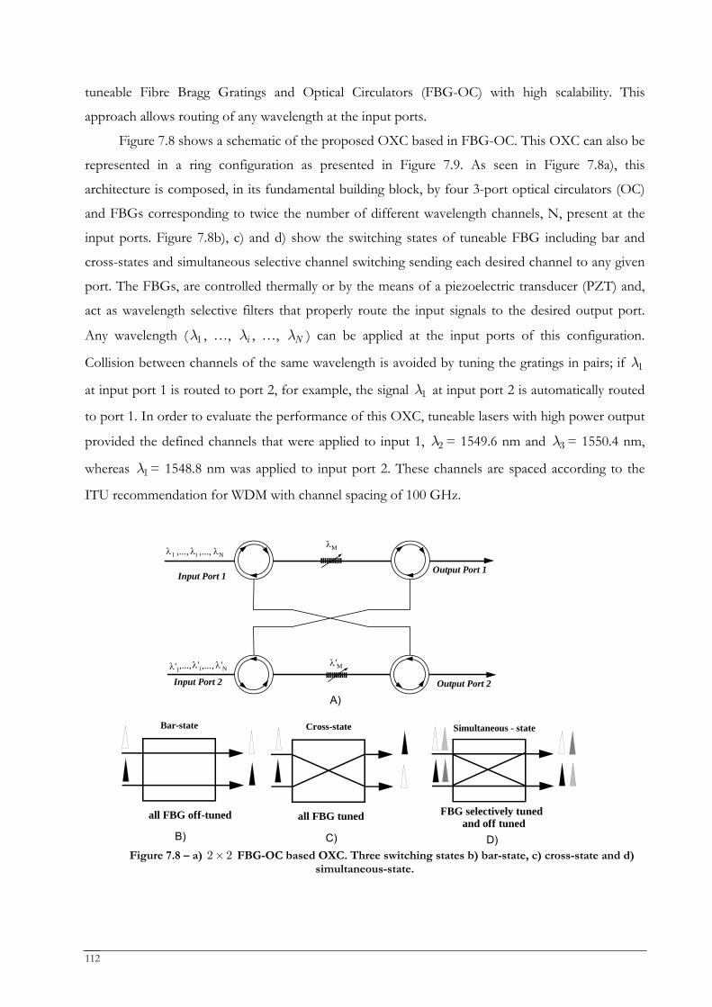
112
tuneable Fibre Bragg Gratings and Optical Circulators (FBG-OC) with high scalability. This
approach allows routing of any wavelength at the input ports.
Figure 7.8 shows a schematic of the proposed OXC based in FBG-OC. This OXC can also be
represented in a ring configuration as presented in Figure 7.9. As seen in Figure 7.8a), this
architecture is composed, in its fundamental building block, by four 3-port optical circulators (OC)
and FBGs corresponding to twice the number of different wavelength channels, N, present at the
input ports. Figure 7.8b), c) and d) show the switching states of tuneable FBG including bar and
cross-states and simultaneous selective channel switching sending each desired channel to any given
port. The FBGs, are controlled thermally or by the means of a piezoelectric transducer (PZT) and,
act as wavelength selective filters that properly route the input signals to the desired output port.
Any wavelength ( 1λ , …, iλ , …, Nλ ) can be applied at the input ports of this configuration.
Collision between channels of the same wavelength is avoided by tuning the gratings in pairs; if 1λ
at input port 1 is routed to port 2, for example, the signal 1λ at input port 2 is automatically routed
to port 1. In order to evaluate the performance of this OXC, tuneable lasers with high power output
provided the defined channels that were applied to input 1, 2λ = 1549.6 nm and 3λ = 1550.4 nm,
whereas 1λ = 1548.8 nm was applied to input port 2. These channels are spaced according to the
ITU recommendation for WDM with channel spacing of 100 GHz.
Input Port 1Output Port 1
Input Port 2 Output Port 2
λ1 ,..., λi λN,...,
λ'1,...,λ'i λ'N,..., λ'M
λM
Bar-state
all FBG off-tuned
Cross-state
all FBG tuned
A)
B) C)
Simultaneous - state
FBG selectively tuned and off tuned
D) Figure 7.8 – a) 2 2× FBG-OC based OXC. Three switching states b) bar-state, c) cross-state and d)
simultaneous-state.
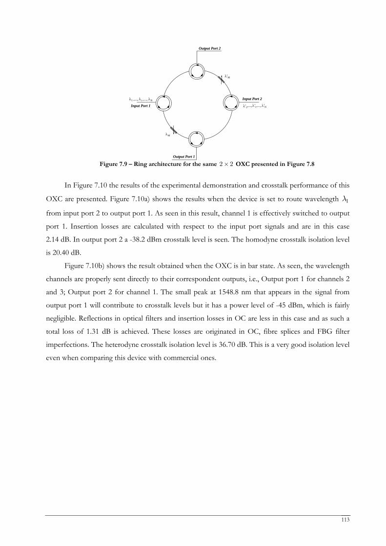
113
Input Port 1
Input Port 2
Output Port 2
Output Port 1
λ1 ,..., λi λN,...,
λ'1,...,λ'i λ'N,...,
λM
λ'M
Figure 7.9 – Ring architecture for the same 2 2× OXC presented in Figure 7.8
In Figure 7.10 the results of the experimental demonstration and crosstalk performance of this
OXC are presented. Figure 7.10a) shows the results when the device is set to route wavelength 1λ
from input port 2 to output port 1. As seen in this result, channel 1 is effectively switched to output
port 1. Insertion losses are calculated with respect to the input port signals and are in this case
2.14 dB. In output port 2 a -38.2 dBm crosstalk level is seen. The homodyne crosstalk isolation level
is 20.40 dB.
Figure 7.10b) shows the result obtained when the OXC is in bar state. As seen, the wavelength
channels are properly sent directly to their correspondent outputs, i.e., Output port 1 for channels 2
and 3; Output port 2 for channel 1. The small peak at 1548.8 nm that appears in the signal from
output port 1 will contribute to crosstalk levels but it has a power level of -45 dBm, which is fairly
negligible. Reflections in optical filters and insertion losses in OC are less in this case and as such a
total loss of 1.31 dB is achieved. These losses are originated in OC, fibre splices and FBG filter
imperfections. The heterodyne crosstalk isolation level is 36.70 dB. This is a very good isolation level
even when comparing this device with commercial ones.
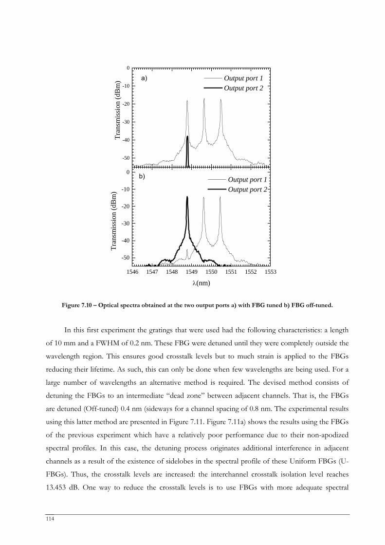
114
1546 1547 1548 1549 1550 1551 1552 1553
-50
-40
-30
-20
-10
0 b)
Output port 1 Output port 2
Tran
smis
sion
(dB
m)
λ(nm)
-50
-40
-30
-20
-10
0
a)
Output port 1 Output port 2
Tran
smis
sion
(dB
m)
Figure 7.10 – Optical spectra obtained at the two output ports a) with FBG tuned b) FBG off-tuned.
In this first experiment the gratings that were used had the following characteristics: a length
of 10 mm and a FWHM of 0.2 nm. These FBG were detuned until they were completely outside the
wavelength region. This ensures good crosstalk levels but to much strain is applied to the FBGs
reducing their lifetime. As such, this can only be done when few wavelengths are being used. For a
large number of wavelengths an alternative method is required. The devised method consists of
detuning the FBGs to an intermediate “dead zone” between adjacent channels. That is, the FBGs
are detuned (Off-tuned) 0.4 nm (sideways for a channel spacing of 0.8 nm. The experimental results
using this latter method are presented in Figure 7.11. Figure 7.11a) shows the results using the FBGs
of the previous experiment which have a relatively poor performance due to their non-apodized
spectral profiles. In this case, the detuning process originates additional interference in adjacent
channels as a result of the existence of sidelobes in the spectral profile of these Uniform FBGs (U-
FBGs). Thus, the crosstalk levels are increased: the interchannel crosstalk isolation level reaches
13.453 dB. One way to reduce the crosstalk levels is to use FBGs with more adequate spectral
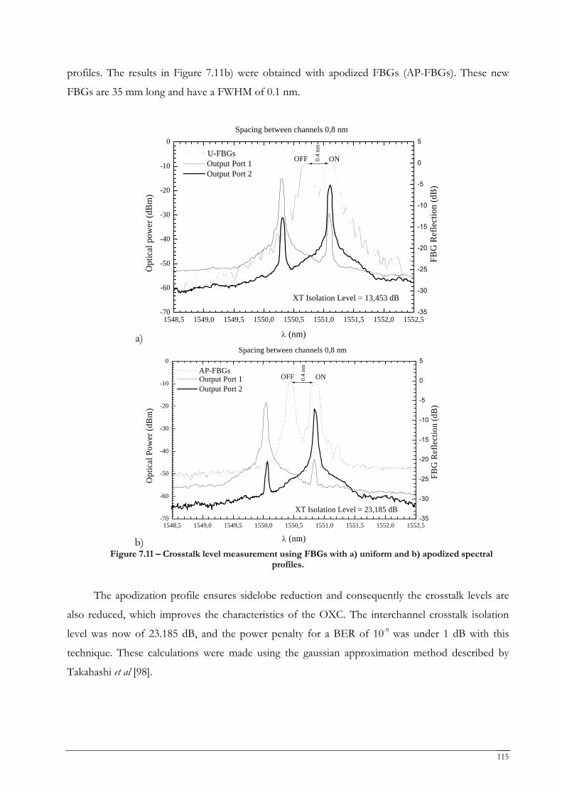
115
profiles. The results in Figure 7.11b) were obtained with apodized FBGs (AP-FBGs). These new
FBGs are 35 mm long and have a FWHM of 0.1 nm.
a)
1548,5 1549,0 1549,5 1550,0 1550,5 1551,0 1551,5 1552,0 1552,5-70
-60
-50
-40
-30
-20
-10
0
Spacing between channels 0,8 nm
0.4
nm
OFF ON
FBG
Ref
lect
ion
(dB
)
Output Port 1 Output Port 2
XT Isolation Level = 13,453 dB
Opt
ical
pow
er (d
Bm
)
λ (nm)
-35
-30
-25
-20
-15
-10
-5
0
5
U-FBGs
b)
1548,5 1549,0 1549,5 1550,0 1550,5 1551,0 1551,5 1552,0 1552,5-70
-60
-50
-40
-30
-20
-10
0
Output Port 1 Output Port 2
XT Isolation Level = 23,185 dB
Opt
ical
Pow
er (d
Bm
)
λ (nm)
-35
-30
-25
-20
-15
-10
-5
0
5Spacing between channels 0,8 nm
0.4
nm
ONOFF
FBG
Ref
lect
ion
(dB
)
AP-FBGs
Figure 7.11 – Crosstalk level measurement using FBGs with a) uniform and b) apodized spectral
profiles.
The apodization profile ensures sidelobe reduction and consequently the crosstalk levels are
also reduced, which improves the characteristics of the OXC. The interchannel crosstalk isolation
level was now of 23.185 dB, and the power penalty for a BER of 10-9 was under 1 dB with this
technique. These calculations were made using the gaussian approximation method described by
Takahashi et al [98].
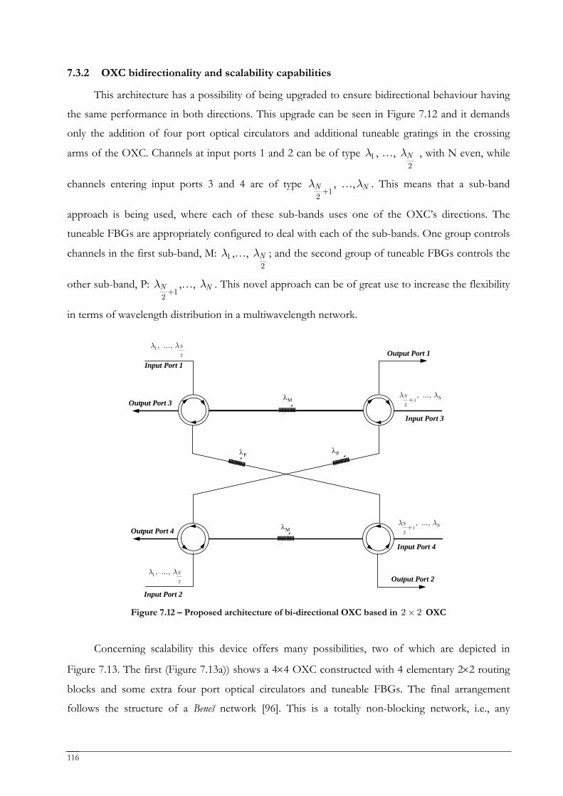
116
7.3.2 OXC bidirectionality and scalability capabilities
This architecture has a possibility of being upgraded to ensure bidirectional behaviour having
the same performance in both directions. This upgrade can be seen in Figure 7.12 and it demands
only the addition of four port optical circulators and additional tuneable gratings in the crossing
arms of the OXC. Channels at input ports 1 and 2 can be of type 1λ , …, 2Nλ , with N even, while
channels entering input ports 3 and 4 are of type 1
2Nλ
+, …, Nλ . This means that a sub-band
approach is being used, where each of these sub-bands uses one of the OXC’s directions. The
tuneable FBGs are appropriately configured to deal with each of the sub-bands. One group controls
channels in the first sub-band, M: 1λ ,…, 2Nλ ; and the second group of tuneable FBGs controls the
other sub-band, P: 1
2Nλ
+,…, Nλ . This novel approach can be of great use to increase the flexibility
in terms of wavelength distribution in a multiwavelength network.
Input Port 1
Input Port 2
λM
λM
Input Port 3
Input Port 4
Output Port 2
Output Port 1
Output Port 3
Output Port 4 λN/2+1 ,..., λN-1
λ1 ,...,λN/2-1
λ1 ,...,λN/2-1
λN/2+1 ,..., λN-1
λPλP
Figure 7.12 – Proposed architecture of bi-directional OXC based in 2 2× OXC
Concerning scalability this device offers many possibilities, two of which are depicted in
Figure 7.13. The first (Figure 7.13a)) shows a 4×4 OXC constructed with 4 elementary 2×2 routing
blocks and some extra four port optical circulators and tuneable FBGs. The final arrangement
follows the structure of a Beneš network [96]. This is a totally non-blocking network, i.e., any
1
2
, ..., Nλ λ
1
2
, ..., Nλ λ
12
, ..., N Nλ λ+
12
, ..., N Nλ λ+
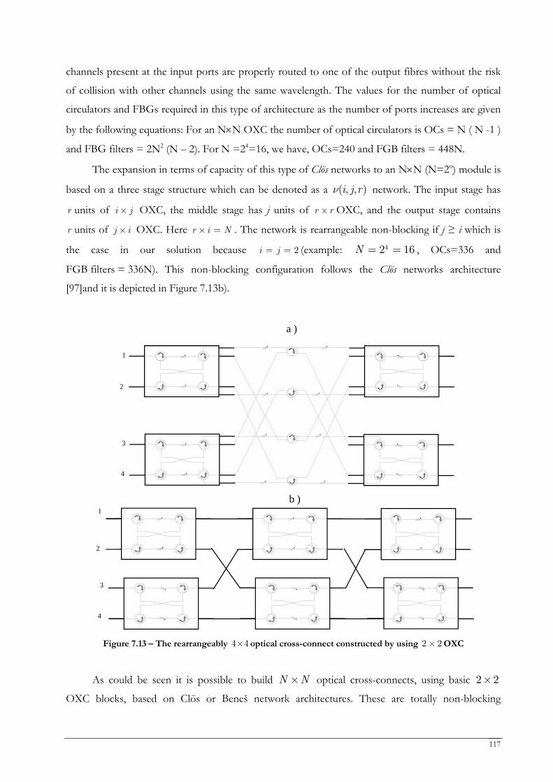
117
channels present at the input ports are properly routed to one of the output fibres without the risk
of collision with other channels using the same wavelength. The values for the number of optical
circulators and FBGs required in this type of architecture as the number of ports increases are given
by the following equations: For an N×N OXC the number of optical circulators is OCs = N ( N -1 )
and FBG filters = 2N2 (N – 2). For N =24=16, we have, OCs=240 and FGB filters = 448N.
The expansion in terms of capacity of this type of Clös networks to an N×N (N=2n) module is
based on a three stage structure which can be denoted as a ( , , )i j rν network. The input stage has
r units of i j× OXC, the middle stage has j units of r r× OXC, and the output stage contains
r units of j i× OXC. Here r i N× = . The network is rearrangeable non-blocking if j ≥ i which is
the case in our solution because 2i j= = (example: 42 16N = = , OCs=336 and
FGB filters = 336N). This non-blocking configuration follows the Clös networks architecture
[97]and it is depicted in Figure 7.13b).
1
4
2
3
0
1
2
3
4
a )
b )
Figure 7.13 – The rearrangeably 4 4× optical cross-connect constructed by using 2 2× OXC
As could be seen it is possible to build N N× optical cross-connects, using basic 2 2×
OXC blocks, based on Clös or Beneš network architectures. These are totally non-blocking
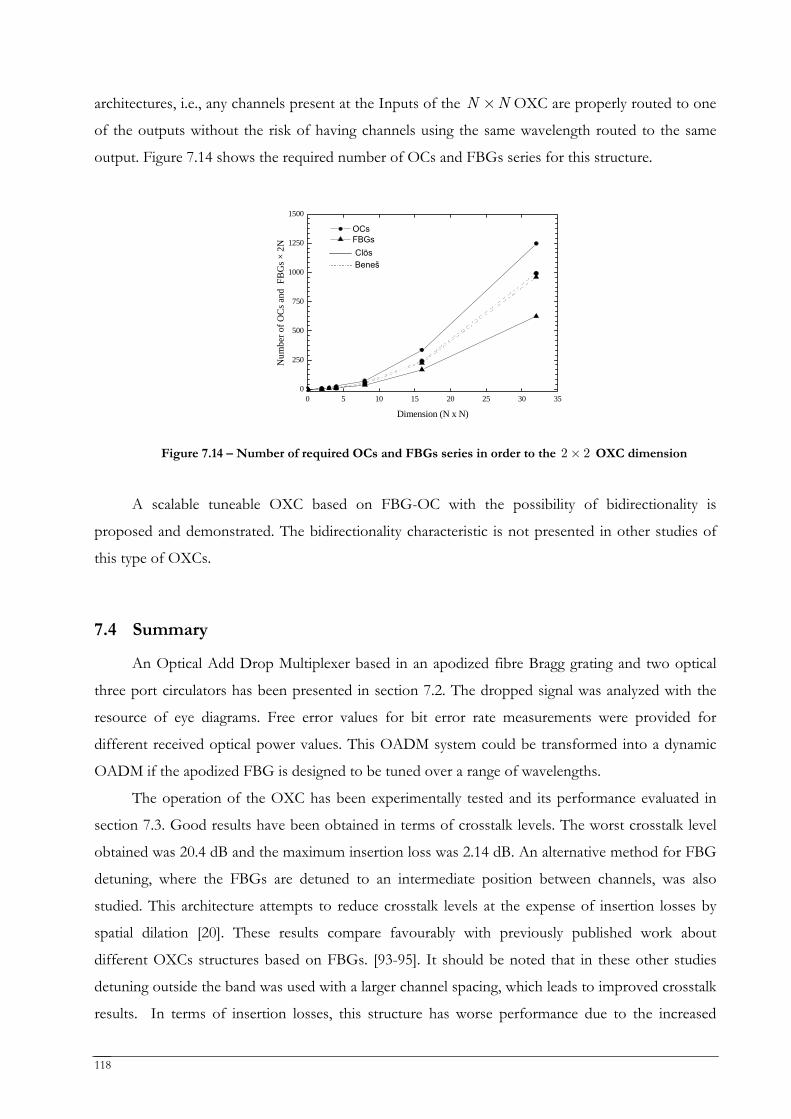
118
architectures, i.e., any channels present at the Inputs of the N N× OXC are properly routed to one
of the outputs without the risk of having channels using the same wavelength routed to the same
output. Figure 7.14 shows the required number of OCs and FBGs series for this structure.
0 5 10 15 20 25 30 350
250
500
750
1000
1250
1500
BenešClös
OCs FBGs
Num
ber o
f OC
s and
FB
Gs ×
2N
Dimension (N x N)
Figure 7.14 – Number of required OCs and FBGs series in order to the 2 2× OXC dimension
A scalable tuneable OXC based on FBG-OC with the possibility of bidirectionality is
proposed and demonstrated. The bidirectionality characteristic is not presented in other studies of
this type of OXCs.
7.4 Summary
An Optical Add Drop Multiplexer based in an apodized fibre Bragg grating and two optical
three port circulators has been presented in section 7.2. The dropped signal was analyzed with the
resource of eye diagrams. Free error values for bit error rate measurements were provided for
different received optical power values. This OADM system could be transformed into a dynamic
OADM if the apodized FBG is designed to be tuned over a range of wavelengths.
The operation of the OXC has been experimentally tested and its performance evaluated in
section 7.3. Good results have been obtained in terms of crosstalk levels. The worst crosstalk level
obtained was 20.4 dB and the maximum insertion loss was 2.14 dB. An alternative method for FBG
detuning, where the FBGs are detuned to an intermediate position between channels, was also
studied. This architecture attempts to reduce crosstalk levels at the expense of insertion losses by
spatial dilation [20]. These results compare favourably with previously published work about
different OXCs structures based on FBGs. [93-95]. It should be noted that in these other studies
detuning outside the band was used with a larger channel spacing, which leads to improved crosstalk
results. In terms of insertion losses, this structure has worse performance due to the increased
119
number of optical circulators and FBGs. These losses, however, can be reduced using multi-port
optical circulators [99].
It is also important to mention that this study allowed the invention of a new architecture that
was patented (see Appendix 2). The new architecture was named “Optical router for WDM systems
with selectivity and wavelength conversion” and was the combination of the OXC presented above
with the fibre ring laser wavelength converter described in the section 6.6.1.
.

8 Concluding remarks
Optical switching is one the crucial topics in the new generation of telecommunication
networks. The developments in fibre optics fabrics, new optical devices and especially the maturity
achieved by WDM technology has allowed the development of new communication systems. Due to
this enormous growth, in Chapter 2 the evolution of the network topologies has been described and
new network architectures, such as the wavelength routed and photonic packet switching networks
were discussed.
Chapter 3 presents the state of the arte in the optical switching technology. A key element in
novel optical networks is the optical switch. Such a device can select the way each lightpath is
conducted through out the network and, obviously, plays a vital role in wavelength routing. Optical
switches can be optoelectronic, when light is converted to an electronic signal, which is then
processed and re-converted to an optical one, or fully transparent, when light is processed
exclusively in an optical way. Optical switches can also be developed as passive devices, when they
are designed in such a way that their own physical features do not allow dynamic reconfiguration,
and in this case they are called static routers. But the most desirable optical switches are
reconfigurable devices, that allow a certain degree of tuneability.
The intrinsic characteristics of a piece of fibre optic can be changed by exposing the fiber to
an intense beam of laser radiation, usually operating with UV spectral region. When permanent
refractive index changes are induced periodically in the fiber core, a fibre Bragg grating is generated.
Different techniques of FBG fabrication and basic theory on this topic were presented in Chapter 4.
As described, fibre Bragg gratings are quite useful optical filters which have the important property
of working either in transmission or reflection. Due to the physical characteristics of the grating, the
Bragg wavelength, which represents the wavelength reflected by the FBG, can be tuned by applying
temperature or mechanical strain to that small structure. This capability makes FBGs very promising
devices for the implementation of all optical switching applications and these facts drives
significantly the laboratorial work.
Wavelength conversion can also be used as an ultrafast optical switching method. Several
nonlinear optical effects may be explored in order to achieve wavelength conversion. In Chapter 5
optoelectronic, optical gating and wave mixing wavelength conversion techniques were described.
Particular emphasis was given to four-wave mixing based WC generated in fibre, since part of the
work developed in this thesis would also deals with the implementation of such technique.
The laboratorial schemes that support this thesis starts being described in Chapter 6. First,
three all-optical switching techniques relying in the FBG thermal tuneability properties were
presented: 1) tuning of a FBG with a Peltier element, 2) tuning of a FBG after a thin film deposition
and applying an electrical current to the structure and 3) tuning of a FBG through a pump laser
diode. Secondly, an all-optical switch based in the mechanical tuning of an FBG with a PZT was
presented. Thirdly two all-optical wavelength converters based on the four wave mixing technique
were demonstrated: one relying in a ring fibre laser architecture that was patented during the course
of this work which uses a DSF as the nonlinear medium, and the other relying in a typical non-
degenerated FWM scheme that uses a PCF as the nonlinear medium. At last, a new technique for
splice standard single mode fibres and PCF was presented.
Chapter 7 shows how the setups used previously could be integrated in all-optical network
devices. The implementation of an OADM based in a apodized FBG is made and BER
measurements were carried out to evaluate the device behaviour in a optical network. Further an
OXC was also implemented and its switching capabilities were tested when is functionality relies,
first in uniform FBG and, then on apodized FBG. Finally a scalability study for the implementation
of such device is carried out.
All-optical switching still being an hot topic in optical communications area. Optical packet
switching and wavelength routed networks still claim for the researchers labour in order to avoid the
optical-electrical-optical conversion. In spite of having slow tuning time, Fibre Bragg gratings,
mostly the apodized ones, due to its spectral characteristics, will certainly continue to play an
important role in such networks specially near the core of the optical networks where the required
switching times could be slower.
New kinds of FBG, namely the sampled FBGs which are structures composed by several
narrow filters having the same reflectivity, surely will be one important area of research in optical
fibre communications. The development of new integrated optics devices and structures that could
operate in a passive or active manner surely must also be one of the research priorities. Good
performance all-optical devices will increase reliability in data transmission as also costs will be
reduced due to the all-optical processing at the network nodes.
Appendix 1 – Conversor de comprimento de onda baseado num laser em
fibra óptica
REQUERENTE
INESC Porto, Instituto de Engenharia de Sistemas e Computadores do Porto, Instituição
Portuguesa, com sede no Campus da FEUP, Rua Dr. Roberto Frias, nº 378, 4200-465 Porto.
AUTORES
Orlando José dos Reis Frazão, Português, residente em Aveiro,
Joel Pedro Peixoto de Carvalho, Português, residente em São Mamede de Infesta,
Igor José Gomes de Faria Terroso, Português, residente em Vila do Conde,
Henrique Manuel de Castro Faria Salgado, Português, residente na Maia.
EPÍGRAFE
CONVERSOR DE COMPRIMENTO DE ONDA BASEADO NUM LASER
EM FIBRA ÓPTICA
RESUMO
A invenção apresentada é de um conversor de comprimento de onda baseado num Laser em fibra
óptica dopada com terras raras numa configuração em anel para operar em sistemas de
multiplexagem densa em comprimento de onda (DWDM). Esta nova configuração apresenta
uma enorme variedade de componentes, entre eles, controladores de estados de polarização (1),
diversos elementos ópticos que podem ser inseridos nos blocos (2), (4) e (5), filtros ópticos (6)
baseados em redes de Bragg em fibra óptica e ainda amplificadores de fibra dopada com terras
raras (7). A configuração apresenta uma grande versatilidade para conversão de comprimento de
onda ao longo de uma extensa gama de comprimentos de onda. Outros dispositivos ópticos
podem ainda ser adicionados a este dispositivo para melhoria das suas características de
funcionamento. Embora a invenção diga respeito a um conversor de comprimento de onda que
utiliza o FWM (Four Wave Mixing – Mistura de Quatro Ondas) degenerado para realizar a
conversão, são ainda apresentadas configurações para conversão de comprimento de onda
recorrendo à geração de FWM não degenerado.
DESCRIÇÃO CONVERSOR DE COMPRIMENTO DE ONDA BASEADO NUM LASER EM
FIBRA ÓPTICA
Campo de Invenção
A presente invenção insere-se na área das redes de comunicação de dados por fibra óptica e
utiliza a tecnologia DWDM (Dense Wavelength Division Multiplexing – Multiplexagem Densa
de Comprimento de Onda) como suporte à conversão de comprimento de onda baseada num
Laser em fibra óptica dopada com terras raras utilizando uma cavidade em anel.
Antecedentes de Investigação
Um dos campos de estudo mais intensivo nos últimos anos, no que diz respeito a melhorar as
capacidades dos sistemas de comunicação de dados utilizando a tecnologia DWDM (Dense
Wavelength Division Multiplexing – Multiplexagem Densa de Comprimento de Onda), tem sido
o da conversão de comprimento de onda totalmente elaborada no domínio óptico.
A conversão de comprimento de onda é essencial para melhoria das capacidades e opções de
encaminhamento em redes totalmente ópticas, especialmente no que diz respeito a melhorar as
habilidades de reconfiguração, impedimento de colisões de sinais ópticos e reutilização de
comprimentos de onda.
O FWM (Four Wave Mixing – Mistura de Quatro Ondas) [K. O. Hill et all, “CW three wave
mixing in single-mode optical fibers”, Journal Applied Physics, Vol. 49, Nº 10, October 1978]
ocorre quando diferentes comprimentos de onda inseridos numa fibra óptica interagem entre si
dando origem a um novo comprimento de onda que não coincide com nenhum dos anteriores.
Embora este fenómeno seja uma enorme desvantagem em sistemas convencionais, para efeitos
de conversão de comprimento de onda torna-se preponderante.
A conversão de comprimento de onda baseada em FWM [K. Inoue, H. Toba, “Wavelength
Conversion Experiment Using Fiber Four-Wave Mixing”, IEEE Photonics Technology Letters,
Vol. 4, Nº 1, January 1992] é sem duvida alguma uma das técnicas mais atractivas devido ás suas
excelentes performances em termos de eficiências de conversão de comprimento de onda,
resposta rápida e simples configuração.
Os Routers Ópticos, elementos chave no ‘backbone’ da rede, são indubitavelmente os elementos
mais beneficiados com o desenvolvimento desta tecnologia, visto que os conversores de
comprimento de onda são dispositivos que devem ser integrados nestes.
Estado da técnica
Os autores não encontraram nenhuma referência bibliográfica ou patente que utilize estas duas
tecnologias simultaneamente, a de um Laser em fibra utilizando uma cavidade em anel e o
recurso à geração de FWM como meio para converter comprimentos de onda.
No entanto existem invenções de Laser em fibra utilizando configurações em anel [US PAT.
6,498,799] bem como também de conversores de comprimento de onda que recorrendo à
utilização de FWM [US PAT. 6,529,314; US PAT. 6,459,525; WO PAT. 02/03132; EP PAT.
1,113,613].
O objectivo geral da invenção do Conversor de Comprimento de Onda utilizando um Laser em
fibra dopada com terras raras utilizando uma cavidade em anel é operar com um sinal num dado
comprimento de onda convertendo-o num outro comprimento de onda, sendo que, toda a
informação modulada no Sinal de Entrada é mantida inalterada no Sinal Convertido.
Descrição Sumária
A presente invenção destina-se a operar em sistemas de multiplexagem densa de comprimento de
onda (DWDM) e constitui conversor de comprimento de onda baseado num Laser em fibra
óptica numa cavidade em anel. Esta é de facto uma nova configuração por apresentar a cavidade
Laser em anel como o grande responsável pela geração do processo não linear que possibilitará a
conversão de comprimento de onda. A arquitectura utiliza uma vasta diversidade de
componentes, nomeadamente, controladores de estados de polarização (1), dispositivos ópticos
que podem ser inseridos como parte integrante dos blocos ((2), (4) e (5)), filtros ópticos (6)
baseados em redes de Bragg em fibra óptica, e ainda amplificadores de fibra dopada com terras
raras (7). A presente invenção é extremamente versátil para conversão de comprimento de onda
ao longo de uma extensa gama de comprimentos de onda. Outros elementos ópticos podem ainda
ser adicionados a este dispositivo para melhorar as suas características de funcionamento. O
conversor de comprimento de onda apresentado, utiliza o FWM (Four Wave Mixing – Mistura de
Quatro Ondas) degenerado para realizar a conversão, no entanto é possível alterar a
configuração para que se obtenha uma conversão de comprimento de onda igualmente eficaz
com recurso à geração de FWM não degenerado.
Descrição Sumária das Figuras
Figura 1 – Conversor de comprimento de onda totalmente óptico baseado num Laser em fibra
numa cavidade em anel usando o FWM degenerado.
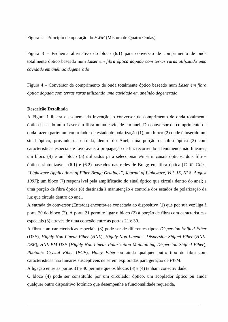
Figura 2 – Princípio de operação do FWM (Mistura de Quatro Ondas)
Figura 3 – Esquema alternativo do bloco (6.1) para conversão de comprimento de onda
totalmente óptico baseado num Laser em fibra óptica dopada com terras raras utilizando uma
cavidade em anelnão degenerado
Figura 4 – Conversor de comprimento de onda totalmente óptico baseado num Laser em fibra
óptica dopada com terras raras utilizando uma cavidade em anelnão degenerado
Descrição Detalhada
A Figura 1 ilustra o esquema da invenção, o conversor de comprimento de onda totalmente
óptico baseado num Laser em fibra numa cavidade em anel. Do conversor de comprimento de
onda fazem parte: um controlador de estado de polarização (1); um bloco (2) onde é inserido um
sinal óptico, provindo da entrada, dentro do Anel; uma porção de fibra óptica (3) com
características especiais e favoráveis à propagação de luz recorrendo a fenómenos não lineares;
um bloco (4) e um bloco (5) utilizados para seleccionar e/inserir canais ópticos; dois filtros
ópticos sintonizáveis (6.1) e (6.2) baseados nas redes de Bragg em fibra óptica [C. R. Giles,
“Lightwave Applications of Fiber Bragg Gratings”, Journal of Lightwave, Vol. 15, Nº 8, August
1997]; um bloco (7) responsável pela amplificação do sinal óptico que circula dentro do anel; e
uma porção de fibra óptica (8) destinada à manutenção e controle dos estados de polarização da
luz que circula dentro do anel.
A entrada do conversor (Entrada) encontra-se conectada ao dispositivo (1) que por sua vez liga à
porta 20 do bloco (2). A porta 21 permite ligar o bloco (2) à porção de fibra com características
especiais (3) através de uma conexão entre as portas 21 e 30.
A fibra com características especiais (3) pode ser de diferentes tipos: Dispersion Shifted Fiber
(DSF), Highly Non-Linear Fiber (HNL), Highly Non-Linear – Dispersion Shifted Fiber (HNL-
DSF), HNL-PM-DSF (Highly Non-Linear Polarization Maintaining Dispersion Shifted Fiber),
Photonic Crystal Fiber (PCF), Holey Fiber ou ainda qualquer outro tipo de fibra com
características não lineares susceptíveis de serem exploradas para geração de FWM.
A ligação entre as portas 31 e 40 permite que os blocos (3) e (4) tenham conectividade.
O bloco (4) pode ser constituído por um circulador óptico, um acoplador óptico ou ainda
qualquer outro dispositivo fotónico que desempenhe a funcionalidade requerida.
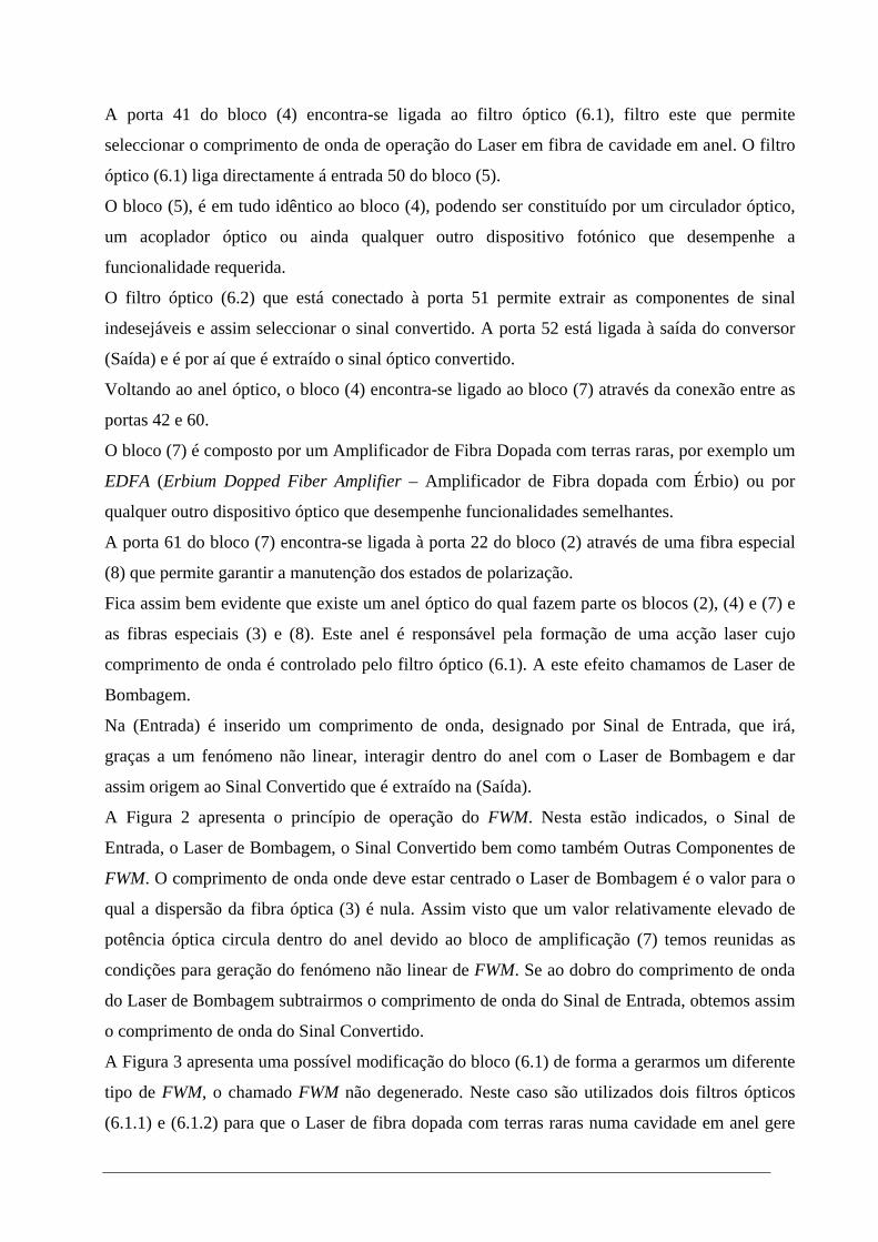
A porta 41 do bloco (4) encontra-se ligada ao filtro óptico (6.1), filtro este que permite
seleccionar o comprimento de onda de operação do Laser em fibra de cavidade em anel. O filtro
óptico (6.1) liga directamente á entrada 50 do bloco (5).
O bloco (5), é em tudo idêntico ao bloco (4), podendo ser constituído por um circulador óptico,
um acoplador óptico ou ainda qualquer outro dispositivo fotónico que desempenhe a
funcionalidade requerida.
O filtro óptico (6.2) que está conectado à porta 51 permite extrair as componentes de sinal
indesejáveis e assim seleccionar o sinal convertido. A porta 52 está ligada à saída do conversor
(Saída) e é por aí que é extraído o sinal óptico convertido.
Voltando ao anel óptico, o bloco (4) encontra-se ligado ao bloco (7) através da conexão entre as
portas 42 e 60.
O bloco (7) é composto por um Amplificador de Fibra Dopada com terras raras, por exemplo um
EDFA (Erbium Dopped Fiber Amplifier – Amplificador de Fibra dopada com Érbio) ou por
qualquer outro dispositivo óptico que desempenhe funcionalidades semelhantes.
A porta 61 do bloco (7) encontra-se ligada à porta 22 do bloco (2) através de uma fibra especial
(8) que permite garantir a manutenção dos estados de polarização.
Fica assim bem evidente que existe um anel óptico do qual fazem parte os blocos (2), (4) e (7) e
as fibras especiais (3) e (8). Este anel é responsável pela formação de uma acção laser cujo
comprimento de onda é controlado pelo filtro óptico (6.1). A este efeito chamamos de Laser de
Bombagem.
Na (Entrada) é inserido um comprimento de onda, designado por Sinal de Entrada, que irá,
graças a um fenómeno não linear, interagir dentro do anel com o Laser de Bombagem e dar
assim origem ao Sinal Convertido que é extraído na (Saída).
A Figura 2 apresenta o princípio de operação do FWM. Nesta estão indicados, o Sinal de
Entrada, o Laser de Bombagem, o Sinal Convertido bem como também Outras Componentes de
FWM. O comprimento de onda onde deve estar centrado o Laser de Bombagem é o valor para o
qual a dispersão da fibra óptica (3) é nula. Assim visto que um valor relativamente elevado de
potência óptica circula dentro do anel devido ao bloco de amplificação (7) temos reunidas as
condições para geração do fenómeno não linear de FWM. Se ao dobro do comprimento de onda
do Laser de Bombagem subtrairmos o comprimento de onda do Sinal de Entrada, obtemos assim
o comprimento de onda do Sinal Convertido.
A Figura 3 apresenta uma possível modificação do bloco (6.1) de forma a gerarmos um diferente
tipo de FWM, o chamado FWM não degenerado. Neste caso são utilizados dois filtros ópticos
(6.1.1) e (6.1.2) para que o Laser de fibra dopada com terras raras numa cavidade em anel gere
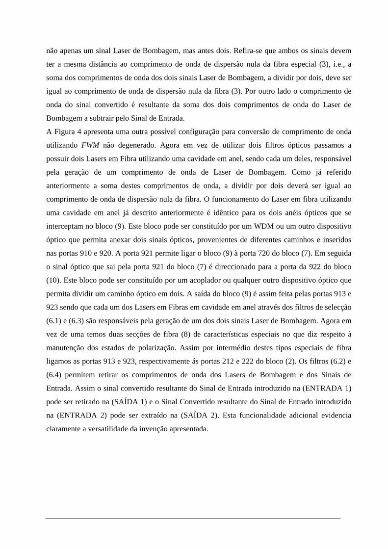
não apenas um sinal Laser de Bombagem, mas antes dois. Refira-se que ambos os sinais devem
ter a mesma distância ao comprimento de onda de dispersão nula da fibra especial (3), i.e., a
soma dos comprimentos de onda dos dois sinais Laser de Bombagem, a dividir por dois, deve ser
igual ao comprimento de onda de dispersão nula da fibra (3). Por outro lado o comprimento de
onda do sinal convertido é resultante da soma dos dois comprimentos de onda do Laser de
Bombagem a subtrair pelo Sinal de Entrada.
A Figura 4 apresenta uma outra possível configuração para conversão de comprimento de onda
utilizando FWM não degenerado. Agora em vez de utilizar dois filtros ópticos passamos a
possuir dois Lasers em Fibra utilizando uma cavidade em anel, sendo cada um deles, responsável
pela geração de um comprimento de onda de Laser de Bombagem. Como já referido
anteriormente a soma destes comprimentos de onda, a dividir por dois deverá ser igual ao
comprimento de onda de dispersão nula da fibra. O funcionamento do Laser em fibra utilizando
uma cavidade em anel já descrito anteriormente é idêntico para os dois anéis ópticos que se
interceptam no bloco (9). Este bloco pode ser constituído por um WDM ou um outro dispositivo
óptico que permita anexar dois sinais ópticos, provenientes de diferentes caminhos e inseridos
nas portas 910 e 920. A porta 921 permite ligar o bloco (9) à porta 720 do bloco (7). Em seguida
o sinal óptico que sai pela porta 921 do bloco (7) é direccionado para a porta da 922 do bloco
(10). Este bloco pode ser constituído por um acoplador ou qualquer outro dispositivo óptico que
permita dividir um caminho óptico em dois. A saída do bloco (9) é assim feita pelas portas 913 e
923 sendo que cada um dos Lasers em Fibras em cavidade em anel através dos filtros de selecção
(6.1) e (6.3) são responsáveis pela geração de um dos dois sinais Laser de Bombagem. Agora em
vez de uma temos duas secções de fibra (8) de características especiais no que diz respeito à
manutenção dos estados de polarização. Assim por intermédio destes tipos especiais de fibra
ligamos as portas 913 e 923, respectivamente ás portas 212 e 222 do bloco (2). Os filtros (6.2) e
(6.4) permitem retirar os comprimentos de onda dos Lasers de Bombagem e dos Sinais de
Entrada. Assim o sinal convertido resultante do Sinal de Entrada introduzido na (ENTRADA 1)
pode ser retirado na (SAÍDA 1) e o Sinal Convertido resultante do Sinal de Entrado introduzido
na (ENTRADA 2) pode ser extraído na (SAÍDA 2). Esta funcionalidade adicional evidencia
claramente a versatilidade da invenção apresentada.
REIVINDICAÇÕES
1. Conversor de comprimento de onda baseado num Laser em fibra óptica dopada com terras
raras utilizando uma cavidade em anel recorrendo ao FWM degenerado, caracterizado por ser
baseado numa vasta diversidade de componentes, nomeadamente, controladores de estados
de polarização (1), dispositivos ópticos que podem ser inseridos como parte integrante dos
blocos ((2), (4) e (5)), filtros ópticos (6) baseados em redes de Bragg em fibra óptica, e ainda
amplificadores de fibra dopada com terras raras (7).
2. Conversor de comprimento de onda baseado num Laser em fibra óptica dopada com terras
raras utilizando uma cavidade em anel recorrendo ao FWM degenerado, de acordo com as
reivindicações 1 e 2, caracterizado pelo facto de habilitar a conversão de comprimento de
onda ao longo de uma vasta gama de comprimentos de onda devido ao uso dos filtros ópticos
sintonizáveis (6.1) e (6.2).
3. Conversor de comprimento de onda baseado num Laser em fibra óptica dopada com terras
raras utilizando uma cavidade em anel recorrendo ao FWM degenerado, de acordo com as
reivindicações 1 e 2, caracterizado pelo facto da fibra de características especiais (3) ser do
tipo Dispersion Shifted Fiber (DSF).
4. Conversor de comprimento de onda baseado num Laser em fibra óptica dopada com terras
raras utilizando uma cavidade em anel recorrendo ao FWM degenerado, de acordo com as
reivindicações 1 e 2, caracterizado pelo facto da fibra de características especiais (3) ser do
tipo Highly Non-Linear Fiber (HNL).
5. Conversor de comprimento de onda baseado num Laser em fibra óptica dopada com terras
raras utilizando uma cavidade em anel recorrendo ao FWM degenerado, de acordo com as
reivindicações 1 e 2, caracterizado pelo facto da fibra de características especiais (3) ser do
tipo HNL-DSF (Highly Non-Linear – Dispersion Shifted Fiber).
6. Conversor de comprimento de onda baseado num Laser em fibra óptica dopada com terras
raras utilizando uma cavidade em anel recorrendo ao FWM degenerado, de acordo com as
reivindicações 1 e 2, caracterizado pelo facto da fibra de características especiais (3) ser do
tipo HNL-PM-DSF (Polarization Maintaining Dispersion Shifted Fiber)
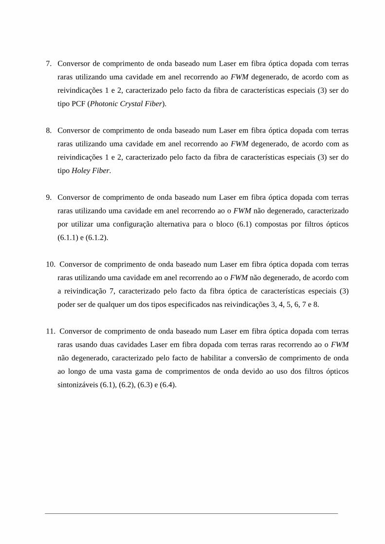
7. Conversor de comprimento de onda baseado num Laser em fibra óptica dopada com terras
raras utilizando uma cavidade em anel recorrendo ao FWM degenerado, de acordo com as
reivindicações 1 e 2, caracterizado pelo facto da fibra de características especiais (3) ser do
tipo PCF (Photonic Crystal Fiber).
8. Conversor de comprimento de onda baseado num Laser em fibra óptica dopada com terras
raras utilizando uma cavidade em anel recorrendo ao FWM degenerado, de acordo com as
reivindicações 1 e 2, caracterizado pelo facto da fibra de características especiais (3) ser do
tipo Holey Fiber.
9. Conversor de comprimento de onda baseado num Laser em fibra óptica dopada com terras
raras utilizando uma cavidade em anel recorrendo ao o FWM não degenerado, caracterizado
por utilizar uma configuração alternativa para o bloco (6.1) compostas por filtros ópticos
(6.1.1) e (6.1.2).
10. Conversor de comprimento de onda baseado num Laser em fibra óptica dopada com terras
raras utilizando uma cavidade em anel recorrendo ao o FWM não degenerado, de acordo com
a reivindicação 7, caracterizado pelo facto da fibra óptica de características especiais (3)
poder ser de qualquer um dos tipos especificados nas reivindicações 3, 4, 5, 6, 7 e 8.
11. Conversor de comprimento de onda baseado num Laser em fibra óptica dopada com terras
raras usando duas cavidades Laser em fibra dopada com terras raras recorrendo ao o FWM
não degenerado, caracterizado pelo facto de habilitar a conversão de comprimento de onda
ao longo de uma vasta gama de comprimentos de onda devido ao uso dos filtros ópticos
sintonizáveis (6.1), (6.2), (6.3) e (6.4).
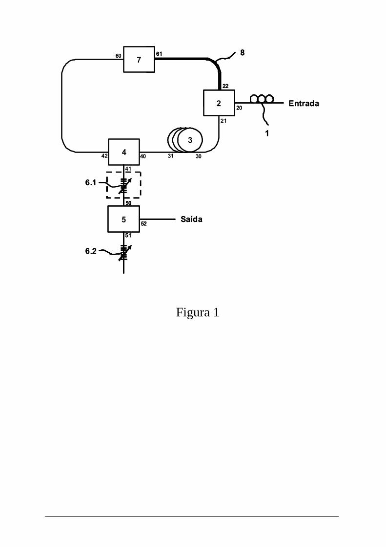
7
4
5 Saída
Entrada
8
1
6.1
6.2
20
21
22
303140
41
42
60 61
50
51
52
333
2
7
4
5 Saída
Entrada
8
1
6.1
6.2
20
21
22
303140
41
42
60 61
50
51
52
333333
2
Figura 1
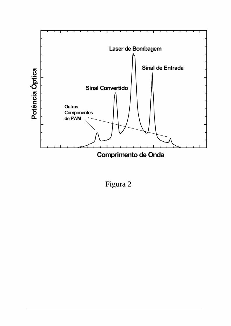
Outras Componentes de FWM
Sinal Convertido
Sinal de Entrada
Laser de Bombagem
Potê
ncia
Ópt
ica
Comprimento de Onda
Figura 2

6.16.1.1
6.1.2
a) b)
6.16.1.1
6.1.2
a) b)
Figura 3
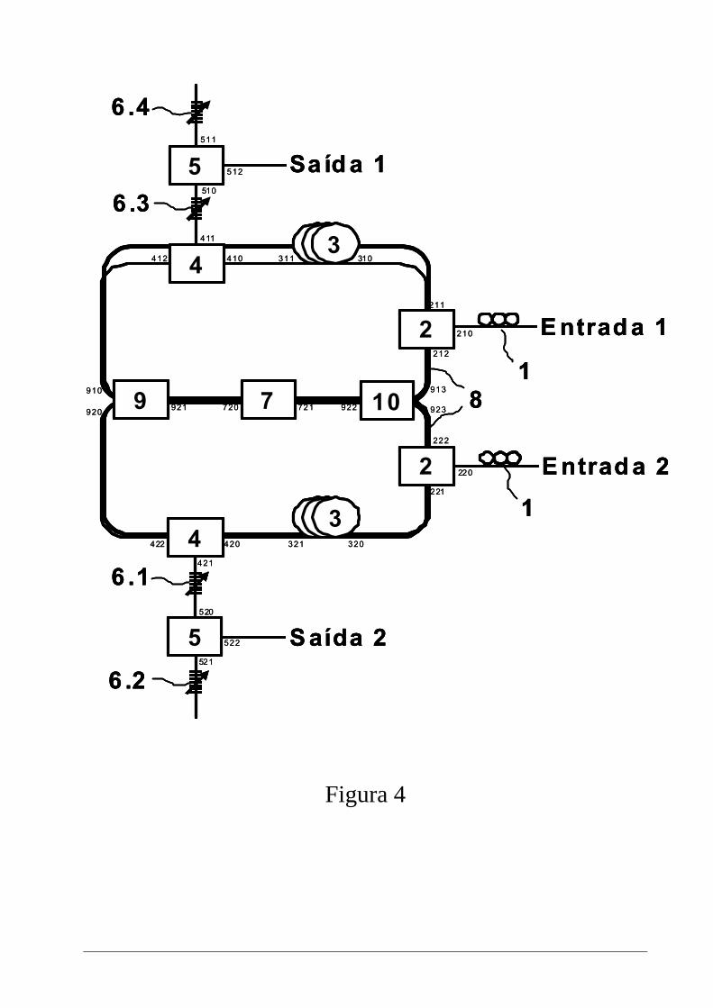
4
2
5 S aída 2
E ntrad a 2
8
1
6 .1
6 .2
7
4
6 .35
6 .4
E ntrad a 1
1
2
Sa íd a 1
9 10
333
333
220
221
222
320321420
421
422
520
522
521
920
910
720 721 922 923
913
212
210
211
310311410412
510
512
511
921
411
4
2
5 S aída 2
E ntrad a 2
8
1
6 .1
6 .2
7
4
6 .35
6 .4
E ntrad a 1
1
2
Sa íd a 1
9 10
333
333
4
2
5 S aída 2
E ntrad a 2
8
1
6 .1
6 .2
7
4
6 .35
6 .4
E ntrad a 1
1
2
Sa íd a 1
9 10
333333
333333
220
221
222
320321420
421
422
520
522
521
920
910
720 721 922 923
913
212
210
211
310311410412
510
512
511
921
411
Figura 4
Appendix 2 – Router Óptico para sistemas DWDM com selectividade e
conversão de comprimento de onda
REQUERENTE
INESC Porto, Instituto de Engenharia de Sistemas e Computadores do Porto, Instituição
Portuguesa, com sede no Campus da FEUP, Rua Dr. Roberto Frias, nº 378, 4200-465 Porto.
AUTORES
Orlando José dos Reis Frazão, Português, residente em Aveiro,
Joel Pedro Peixoto de Carvalho, Português, residente em São Mamede de Infesta,
Igor José Gomes de Faria Terroso, Português, residente em Vila do Conde,
Henrique Manuel de Castro Faria Salgado, Português, residente na Maia.
EPÍGRAFE
ROUTER ÓPTICO PARA SISTEMAS DWDM COM SELECTIVIDADE E
CONVERSÃO DE COMPRIMENTO DE ONDA.
RESUMO
A invenção descrita é composta por um router totalmente óptico para aplicação em redes de
comunicação ópticas que operam com a tecnologia de multiplexagem densa em comprimento de
onda (DWDM). Esta nova configuração proposta é composta por diversos dispositivos fotónicos,
tais como, circuladores ópticos (104), isoladores ópticos (102), conversores de comprimento de
onda (200) e filtros ópticos (3) baseados em redes de Bragg em fibra óptica. A arquitectura
apresenta grande versatilidade para seleccionar canais multiplexados em comprimento de onda, e
inclui a impossibilidade de interferência entre canais de mesmo comprimento de onda, devido às
funcionalidades desempenhadas pelos blocos (100) e (101). Outras características desta
configuração são a capacidade tornar o funcionamento dispositivo bidireccional e ainda de
possibilitar adicionar e/ou remover canais ópticos multiplexados. Este router óptico pode ainda
utilizar outros dispositivos ópticos que permitirão a melhoria do seu desempenho. Este
dispositivo é ainda totalmente escalável a configurações de N × N portas, podendo N ser par ou
ímpar.
DESCRIÇÃO ROUTER ÓPTICO PARA SISTEMAS DWDM COM SELECTIVIDADE E
CONVERSÃO DE COMPRIMENTO DE ONDA
Campo de Invenção
A presente invenção insere-se na área das telecomunicações por fibra óptica e diz respeito a um
router óptico de baixa diafonia para sistemas DWDM (multiplexagem densa em comprimento de
onda) com selectividade e conversão de comprimento de onda. O objectivo geral da invenção é
operar com sinais multi-comprimento de onda, sendo capaz de os encaminhar, comutar,
converter, adicionar e/ou remover. É ainda objectivo da presente invenção, a bidireccionalidade
do router óptico bem como também a sua expansibilidade para N × N portas, sendo N par ou
ímpar.
Antecedentes de Investigação
O incremento nas taxas de transmissão de dados tornou as redes de telecomunicações totalmente
ópticas, baseadas na tecnologia de multiplexagem densa de comprimento de onda (DWDM), no
candidato maioritário à constituição do backbone que suportará o tráfego global de dados num
futuro próximo. O DWDM e o consequente recurso às técnicas de encaminhamento por
comprimento de onda, tornam os comutadores ópticos (OXC) com selecção de comprimento de
onda, dispositivos chave neste tipo de redes, dado que permitem aos pontos terminais de rede a
possibilidade de comunicarem de forma transparente, flexível e reconfigurável.
A necessidade de re-encaminhar dois comprimentos de onda iguais de portas adjacentes para
uma mesma porta de saída, apresentou-se desde logo, como uma forte limitação na construção
destes comutadores. Com o aparecimento de conversores em comprimento de onda foi possível
eliminar este problema. Conjugando estas duas tecnologias – comutação óptica e conversão de
comprimento de onda – torna-se possível a construção de routers totalmente ópticos.
Estado da técnica
Embora já existam invenções de routers para as redes de comunicação por fibra óptica, é de
salientar o facto dos routers até agora projectados utilizarem técnicas de conversão
optoelectrónicas (envolvendo conversão electro-óptica e consequentemente opto-electrónica) ou
no caso de operarem no domínio exclusivamente óptico, as funcionalidades mais complexas –
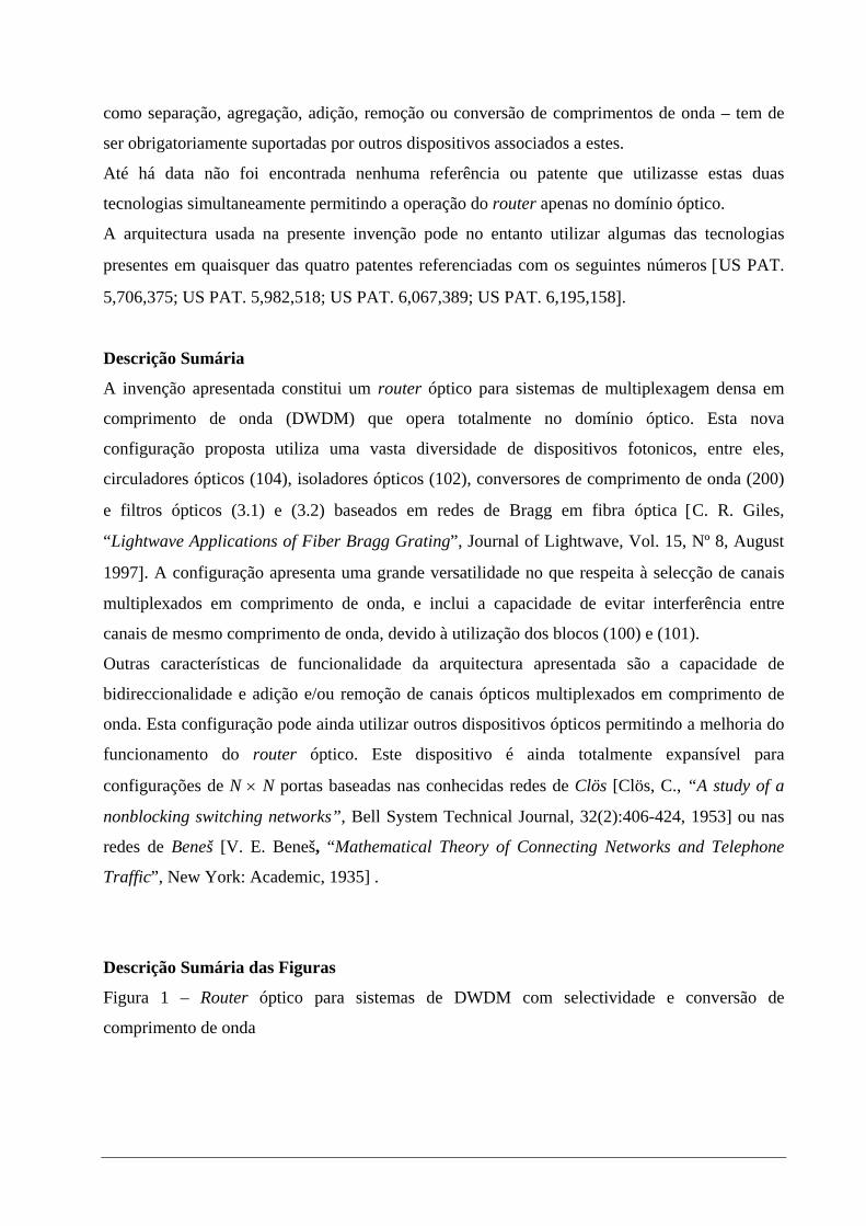
como separação, agregação, adição, remoção ou conversão de comprimentos de onda – tem de
ser obrigatoriamente suportadas por outros dispositivos associados a estes.
Até há data não foi encontrada nenhuma referência ou patente que utilizasse estas duas
tecnologias simultaneamente permitindo a operação do router apenas no domínio óptico.
A arquitectura usada na presente invenção pode no entanto utilizar algumas das tecnologias
presentes em quaisquer das quatro patentes referenciadas com os seguintes números [US PAT.
5,706,375; US PAT. 5,982,518; US PAT. 6,067,389; US PAT. 6,195,158].
Descrição Sumária
A invenção apresentada constitui um router óptico para sistemas de multiplexagem densa em
comprimento de onda (DWDM) que opera totalmente no domínio óptico. Esta nova
configuração proposta utiliza uma vasta diversidade de dispositivos fotonicos, entre eles,
circuladores ópticos (104), isoladores ópticos (102), conversores de comprimento de onda (200)
e filtros ópticos (3.1) e (3.2) baseados em redes de Bragg em fibra óptica [C. R. Giles,
“Lightwave Applications of Fiber Bragg Grating”, Journal of Lightwave, Vol. 15, Nº 8, August
1997]. A configuração apresenta uma grande versatilidade no que respeita à selecção de canais
multiplexados em comprimento de onda, e inclui a capacidade de evitar interferência entre
canais de mesmo comprimento de onda, devido à utilização dos blocos (100) e (101).
Outras características de funcionalidade da arquitectura apresentada são a capacidade de
bidireccionalidade e adição e/ou remoção de canais ópticos multiplexados em comprimento de
onda. Esta configuração pode ainda utilizar outros dispositivos ópticos permitindo a melhoria do
funcionamento do router óptico. Este dispositivo é ainda totalmente expansível para
configurações de N × N portas baseadas nas conhecidas redes de Clös [Clös, C., “A study of a
nonblocking switching networks”, Bell System Technical Journal, 32(2):406-424, 1953] ou nas
redes de Beneš [V. E. Beneš, “Mathematical Theory of Connecting Networks and Telephone
Traffic”, New York: Academic, 1935] .
Descrição Sumária das Figuras
Figura 1 – Router óptico para sistemas de DWDM com selectividade e conversão de
comprimento de onda
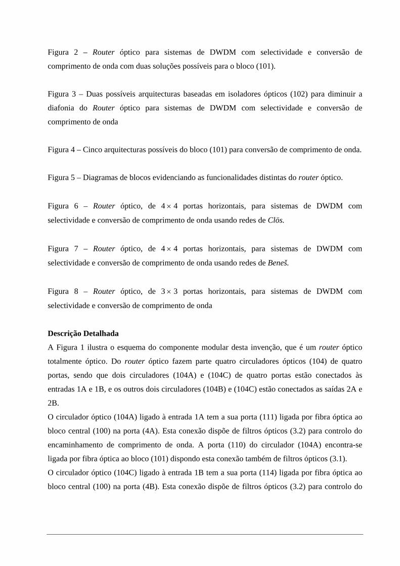
Figura 2 – Router óptico para sistemas de DWDM com selectividade e conversão de
comprimento de onda com duas soluções possíveis para o bloco (101).
Figura 3 – Duas possíveis arquitecturas baseadas em isoladores ópticos (102) para diminuir a
diafonia do Router óptico para sistemas de DWDM com selectividade e conversão de
comprimento de onda
Figura 4 – Cinco arquitecturas possíveis do bloco (101) para conversão de comprimento de onda.
Figura 5 – Diagramas de blocos evidenciando as funcionalidades distintas do router óptico.
Figura 6 – Router óptico, de 4 × 4 portas horizontais, para sistemas de DWDM com
selectividade e conversão de comprimento de onda usando redes de Clös.
Figura 7 – Router óptico, de 4 × 4 portas horizontais, para sistemas de DWDM com
selectividade e conversão de comprimento de onda usando redes de Beneš.
Figura 8 – Router óptico, de 3 × 3 portas horizontais, para sistemas de DWDM com
selectividade e conversão de comprimento de onda
Descrição Detalhada
A Figura 1 ilustra o esquema do componente modular desta invenção, que é um router óptico
totalmente óptico. Do router óptico fazem parte quatro circuladores ópticos (104) de quatro
portas, sendo que dois circuladores (104A) e (104C) de quatro portas estão conectados às
entradas 1A e 1B, e os outros dois circuladores (104B) e (104C) estão conectados as saídas 2A e
2B.
O circulador óptico (104A) ligado à entrada 1A tem a sua porta (111) ligada por fibra óptica ao
bloco central (100) na porta (4A). Esta conexão dispõe de filtros ópticos (3.2) para controlo do
encaminhamento de comprimento de onda. A porta (110) do circulador (104A) encontra-se
ligada por fibra óptica ao bloco (101) dispondo esta conexão também de filtros ópticos (3.1).
O circulador óptico (104C) ligado à entrada 1B tem a sua porta (114) ligada por fibra óptica ao
bloco central (100) na porta (4B). Esta conexão dispõe de filtros ópticos (3.2) para controlo do
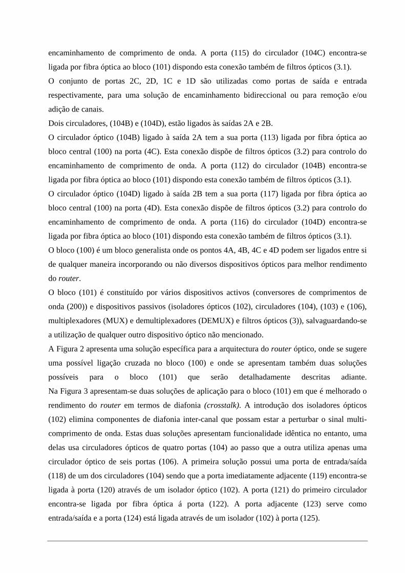
encaminhamento de comprimento de onda. A porta (115) do circulador (104C) encontra-se
ligada por fibra óptica ao bloco (101) dispondo esta conexão também de filtros ópticos (3.1).
O conjunto de portas 2C, 2D, 1C e 1D são utilizadas como portas de saída e entrada
respectivamente, para uma solução de encaminhamento bidireccional ou para remoção e/ou
adição de canais.
Dois circuladores, (104B) e (104D), estão ligados às saídas 2A e 2B.
O circulador óptico (104B) ligado à saída 2A tem a sua porta (113) ligada por fibra óptica ao
bloco central (100) na porta (4C). Esta conexão dispõe de filtros ópticos (3.2) para controlo do
encaminhamento de comprimento de onda. A porta (112) do circulador (104B) encontra-se
ligada por fibra óptica ao bloco (101) dispondo esta conexão também de filtros ópticos (3.1).
O circulador óptico (104D) ligado à saída 2B tem a sua porta (117) ligada por fibra óptica ao
bloco central (100) na porta (4D). Esta conexão dispõe de filtros ópticos (3.2) para controlo do
encaminhamento de comprimento de onda. A porta (116) do circulador (104D) encontra-se
ligada por fibra óptica ao bloco (101) dispondo esta conexão também de filtros ópticos (3.1).
O bloco (100) é um bloco generalista onde os pontos 4A, 4B, 4C e 4D podem ser ligados entre si
de qualquer maneira incorporando ou não diversos dispositivos ópticos para melhor rendimento
do router.
O bloco (101) é constituído por vários dispositivos activos (conversores de comprimentos de
onda (200)) e dispositivos passivos (isoladores ópticos (102), circuladores (104), (103) e (106),
multiplexadores (MUX) e demultiplexadores (DEMUX) e filtros ópticos (3)), salvaguardando-se
a utilização de qualquer outro dispositivo óptico não mencionado.
A Figura 2 apresenta uma solução específica para a arquitectura do router óptico, onde se sugere
uma possível ligação cruzada no bloco (100) e onde se apresentam também duas soluções
possíveis para o bloco (101) que serão detalhadamente descritas adiante.
Na Figura 3 apresentam-se duas soluções de aplicação para o bloco (101) em que é melhorado o
rendimento do router em termos de diafonia (crosstalk). A introdução dos isoladores ópticos
(102) elimina componentes de diafonia inter-canal que possam estar a perturbar o sinal multi-
comprimento de onda. Estas duas soluções apresentam funcionalidade idêntica no entanto, uma
delas usa circuladores ópticos de quatro portas (104) ao passo que a outra utiliza apenas uma
circulador óptico de seis portas (106). A primeira solução possui uma porta de entrada/saída
(118) de um dos circuladores (104) sendo que a porta imediatamente adjacente (119) encontra-se
ligada à porta (120) através de um isolador óptico (102). A porta (121) do primeiro circulador
encontra-se ligada por fibra óptica á porta (122). A porta adjacente (123) serve como
entrada/saída e a porta (124) está ligada através de um isolador (102) à porta (125).
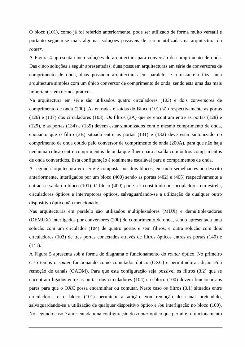
O bloco (101), como já foi referido anteriormente, pode ser utilizado de forma muito versátil e
portanto seguem-se mais algumas soluções passíveis de serem utilizadas na arquitectura do
router.
A Figura 4 apresenta cinco soluções de arquitectura para conversão de comprimento de onda.
Das cinco soluções a seguir apresentadas, duas possuem arquitecturas em série de conversores de
comprimento de onda, duas possuem arquitecturas em paralelo, e a restante utiliza uma
arquitectura simples com um único conversor de comprimento de onda, sendo esta uma das mais
importantes em termos práticos.
Na arquitectura em série são utilizados quatro circuladores (103) e dois conversores de
comprimento de onda (200). As entradas e saídas do Bloco (101) são respectivamente as portas
(126) e (137) dos circuladores (103). Os filtros (3A) que se encontram entre as portas (128) e
(129), e as portas (134) e (135) devem estar sintonizados com o mesmo comprimento de onda,
enquanto que o filtro (3B) situado entre as portas (131) e (132) deve estar sintonizado no
comprimento de onda obtido pelo conversor de comprimento de onda (200A), para que não haja
nenhuma colisão entre comprimentos de onda que fluem para a saída com outros comprimentos
de onda convertidos. Esta configuração é totalmente escalável para n comprimentos de onda.
A segunda arquitectura em série é composta por dois blocos, em tudo semelhantes ao descrito
anteriormente, interligados por um bloco (400) sendo as portas (402) e (405) respectivamente a
entrada e saída do bloco (101). O bloco (400) pode ser constituído por acopladores em estrela,
circuladores ópticos e interruptores ópticos, salvaguardando-se a utilização de qualquer outro
dispositivo óptico não mencionado.
Nas arquitecturas em paralelo são utilizados multiplexadores (MUX) e demultiplexadores
(DEMUX) interligados por conversores (200) de comprimento de onda, sendo apresentada uma
solução com um circulador (104) de quatro portas e sem filtros, e outra solução com dois
circuladores (103) de três portas conectados através de filtros ópticos entres as portas (140) e
(141).
A Figura 5 apresenta sob a forma de diagrama o funcionamento do router óptico. No primeiro
caso temos o router funcionando como comutador óptico (OXC) e permitindo a adição e/ou
remoção de canais (OADM). Para que esta configuração seja possível os filtros (3.2) que se
encontram ligados entre as portas dos circuladores (104) e o bloco (100) devem funcionar aos
pares para que o OXC possa encaminhar ou comutar. Neste caso os filtros (3.1) situados entre
circuladores e o bloco (101) permitem a adição e/ou remoção do canal pretendido,
salvaguardando-se a utilização de qualquer dispositivo óptico e /ou interligação no bloco (100).
No segundo caso é apresentada uma configuração do router óptico que permite o funcionamento
bidireccional do dispositivo obrigando todos os filtros (3.1) funcionam de maneira sincronizada
bem como também os filtros (3.2) a funcionarem de maneira semelhante.
A Figura 6 apresenta um exemplo de escalabilidade usando as redes de Clös. O modelo de 4 × 4
portas horizontais é composto por seis blocos do router óptico. Nesta configuração é possível
introduzir qualquer comprimento de onda em qualquer uma das entradas não correndo o risco de
colisão entre eles caso estes sejam semelhantes, sem restrições no encaminhamento. Esta
arquitectura possui 4 entradas, a possibilidade de introdução de n comprimentos de onda e usa no
mínimo vinte e quatro circuladores ópticos (104) e no mínimo 48 n filtros ópticos, ( 24 n filtros
(3.1) e 24 n filtros (3.2)). Esta configuração é totalmente escalável conforme especificado na
teoria das redes de Clös.
A Figura 7 apresenta uma outra arquitectura para o router baseada nas redes de Beneš. Segundo
a arquitectura proposta por Beneš os nós da rede são constituídos por routers elementares, o que
não acontece na configuração proposta. Conforme verificado os nós das redes Beneš são
substituídos por circuladores ópticos, que não realizam comutação, antes, apenas
encaminhamento. De notar que nesta forma a rede deixa de ser unicamente constituída por
blocos elementares do router e passa a conter blocos intermédios (500) compostos por filtros e
circuladores ópticos, salvaguardando a utilização de qualquer outro dispositivo óptico para
melhoramento do router óptico. A grande vantagem desta configuração é o uso de menos
circuladores em relação à anterior. Esta configuração é totalmente escalável conforme
especificado na teoria das redes de Beneš.
A Figura 8 apresenta uma estrutura de 3 × 3 portas horizontais sem possibilidade de bloqueio
evidenciando que a arquitectura modular do router óptico descrito inicialmente é ainda
expansível para N portas ímpares.
REIVINDICAÇÕES
1. Router óptico para sistemas DWDM com selectividade e conversão de comprimento de onda,
caracterizado pelo facto de ser baseado em quatro circuladores ópticos (104), isoladores
ópticos (102), conversores de comprimento de onda (200) e filtros ópticos (3.1) e (3.2)
baseados em redes de Bragg em fibra óptica.
2. Router óptico para sistemas DWDM com selectividade e conversão de comprimento de onda,
de acordo com a reivindicação 1, caracterizado por possuir na sua configuração dois blocos
(100) e (101) com múltiplas funcionalidades.
3. Router óptico para sistemas DWDM com selectividade e conversão de comprimento de onda,
de acordo com a reivindicação 1, caracterizado por operar numa vasta gana de comprimentos
de onda (λ1, λ2,..., λM) e evidenciando baixa diafonia.
4. Router óptico para sistemas DWDM com selectividade e conversão de comprimento de onda,
de acordo com as reivindicações 1, 2 e 3, caracterizado por possuir oito conjuntos de filtros
ópticos (3.1) e (3.2), cada um deles responsáveis por um comprimento onda.
5. Router óptico para sistemas DWDM com selectividade e conversão de comprimento de onda,
de acordo com a reivindicação 1, caracterizado pelo facto de prevenir a interferência
destrutiva entre diferentes canais que usem o mesmo comprimento de onda.
6. Router óptico para sistemas DWDM com selectividade e conversão de comprimento de onda,
de acordo com as reivindicações 1, 2, 3 e 5, caracterizado pelo facto de serem nele aplicados
diversos componentes passivos (circuladores ópticos (103), (104), (106), filtros ópticos ((3),
(3A) e (3B)), isoladores ópticos (102), multiplexadores (MUX) e demultiplexadores
(DEMUX)) ou activos (amplificadores, conversores (200) e interruptores ópticos,
acopladores em estrela (400)) como parte constituinte dos módulos (100) e (101).
7. Router óptico para sistemas DWDM com selectividade e conversão de comprimento de onda,
de acordo com as reivindicações 1, 2, 3, 5 e 6, caracterizado por um funcionamento
bidireccional.
8. Router óptico para sistemas DWDM com selectividade e conversão de comprimento de onda,
de acordo com as reivindicações 1, 2, 3, 5 e 6, caracterizado pelo facto de permitir a adição
e/ou remoção de canais.
9. Router óptico para sistemas DWDM com selectividade e conversão de comprimento de onda,
de acordo com as reivindicações 1, 5, 7 e 8, caracterizado por uma arquitectura do bloco
(101) que permite a redução da diafonia utilizando isoladores (102) e circuladores (104) e
(106).
10. Router óptico para sistemas DWDM com selectividade e conversão de comprimento de
onda, de acordo com as reivindicações 1, 2, 3, 5 e 6, caracterizado por uma arquitectura em
série dos conversores de comprimento de onda aplicados no bloco (101).
11. Router óptico para sistemas DWDM com selectividade e conversão de comprimento de
onda, de acordo com as reivindicações 1, 2, 3, 5 e 6, caracterizado por uma arquitectura em
paralelo dos conversores de comprimento de onda aplicados no bloco (101).
12. Router óptico para sistemas DWDM com selectividade e conversão de comprimento de
onda, de acordo com as reivindicações 1, 2, 3, 5 e 6, caracterizado por uma arquitectura
simples com conversão de comprimento de onda aplicada no bloco (101).
13. Router óptico para sistemas DWDM com selectividade e conversão de comprimento de
onda, de acordo com as reivindicações 1, 2, 3, 5 e 6, caracterizado pelo facto de ser
totalmente expansível a N × N portas, sendo N par, de acordo com as especificações para as
redes Beneš e Clös, impedindo o cruzamento destrutivo de canais.
14. Router óptico para sistemas DWDM com selectividade e conversão de comprimento de
onda, de acordo com as reivindicações 1, 2, 3, 5 e 6, caracterizado pelo facto de ser
totalmente expansível a N × N portas, sendo N ímpar.
15. Router óptico para sistemas DWDM com selectividade e conversão de comprimento de
onda, de acordo com as reivindicações 1, 2, 3, 5 e 6, caracterizado pelo facto de ser baseado
em circuladores multi-porta.
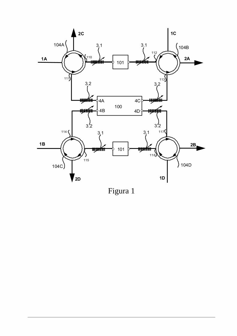
1A 2A
1B 2B
1C2C
2D 1D
1004A 4C
4B 4D
3.2
104A
104C 104D
104B
111
110112
113
117
116
114
115
101
101
3.1
3.2
3.2 3.23.1 3.1
3.1
Figura 1
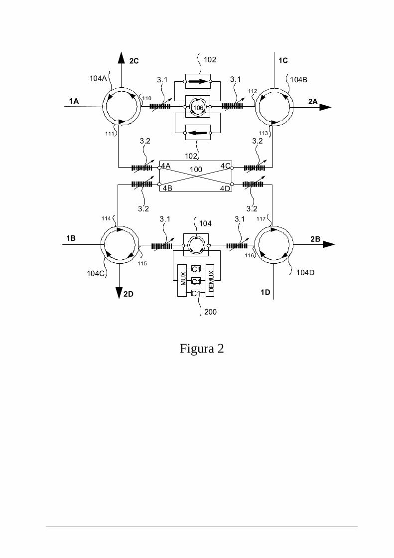
1A 2A
1B 2B
1C2C
2D 1D
100
DEM
UX
MU
X C1
C1C1
4A 4C
4B 4D
3.1104A
104C 104D
104B
104
102
102
200
111
110112
113
117
116
114
115
106
3.1
3.1 3.1
3.2 3.2
3.2 3.2
Figura 2
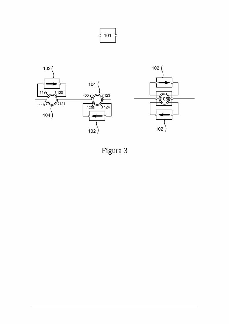
101
104
104
106
102
102 102
102
119
118
120
121
122 123
124125
Figura 3
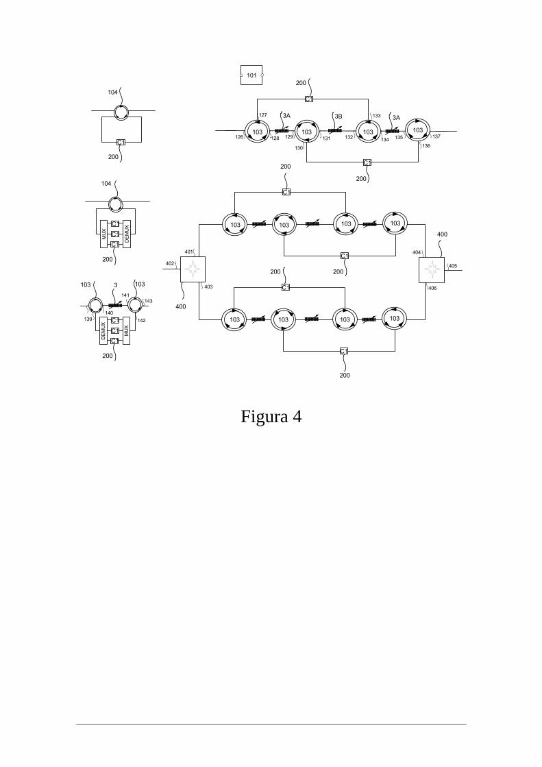
101
DEM
UX
MU
X
C1
C1C1
C1
C1
C1
C1
C1
C1
DEM
UX
MU
X
C1
C1C1
C1
104
104
200
200
200
103 3 103
103 103 103 103
103 103103
200
200
400
400
200 200
200
200
103
103 103 103 103
3A 3B 3A
126
127
128 129
130
131 132
133
135
136
137134
404
405
406
401
402
403
139140
141
142
143
Figura 4
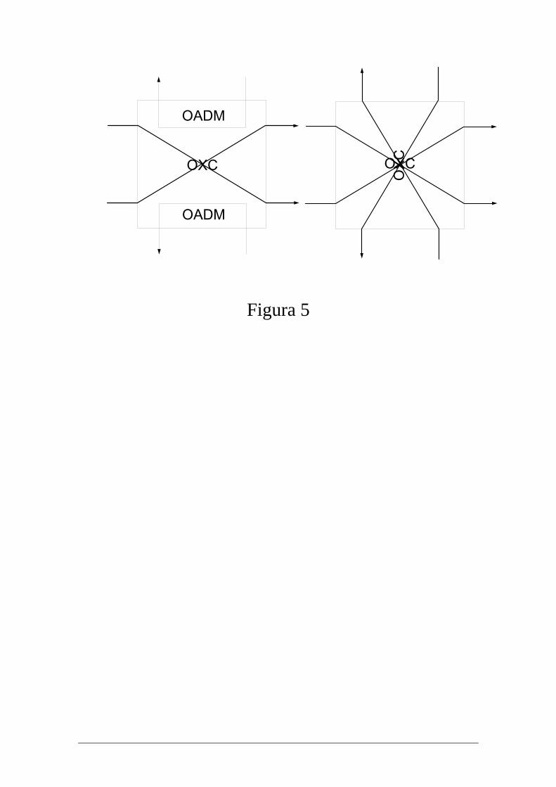
OXC
OADM
OADM
OXC
OXC
Figura 5
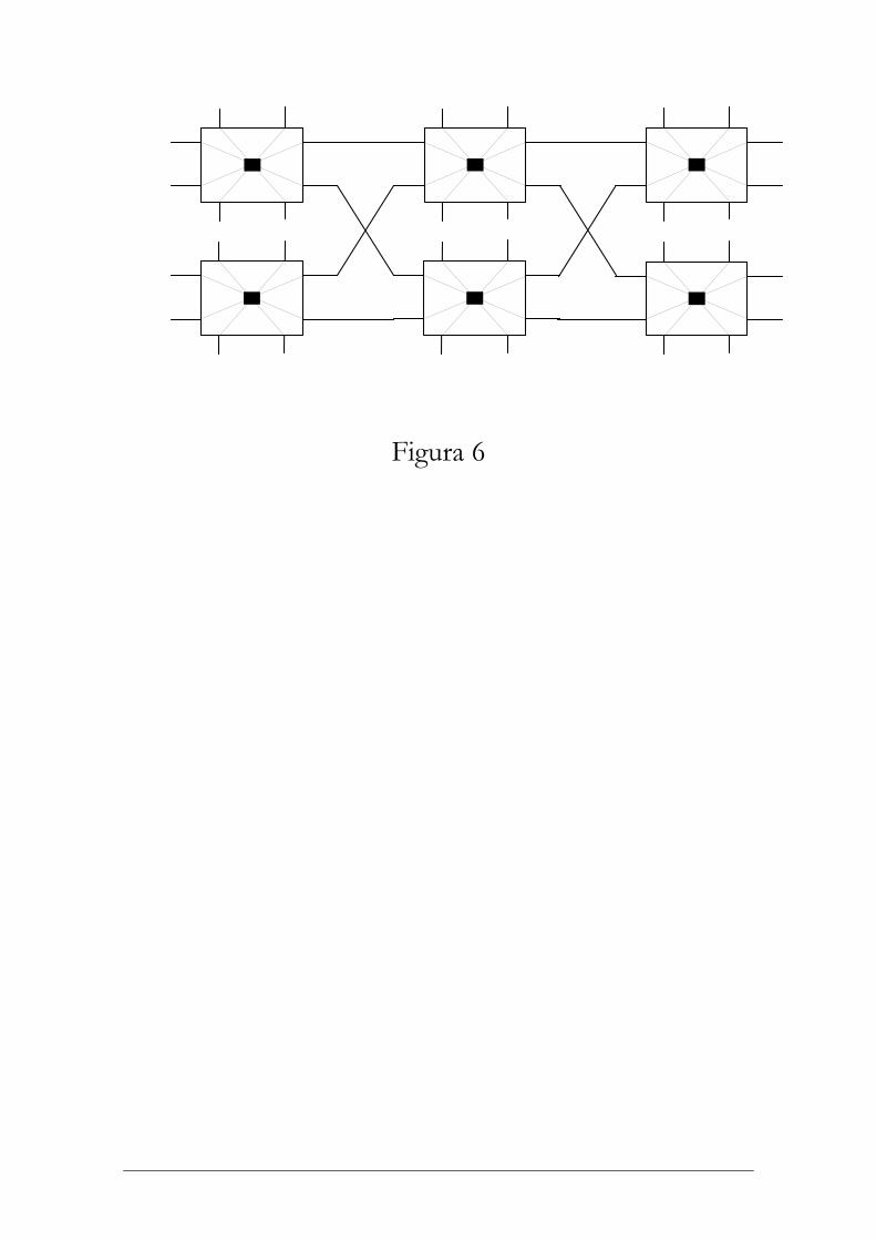
Figura 6
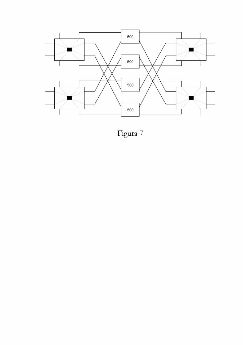
500
500
500
500
Figura 7
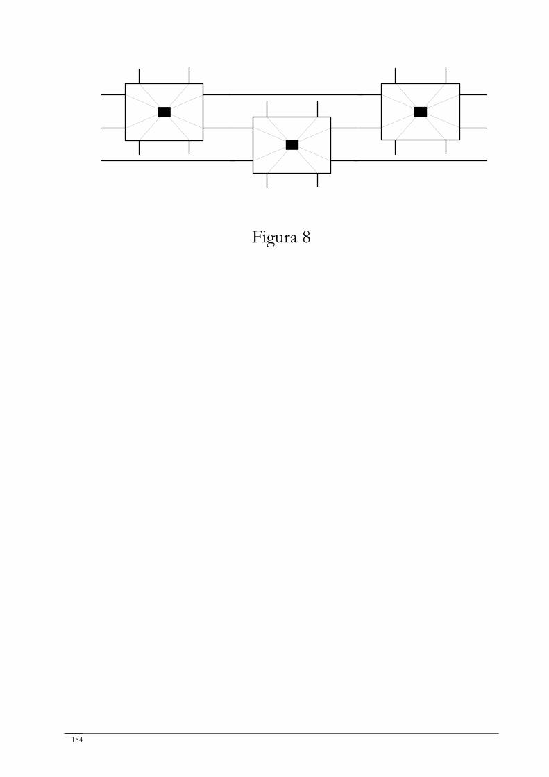
154
Figura 8
Bibliography
1. Yadlowsky, M.J., E.M. Deliso, and V.L. DaSilva, Optical fibers and amplifiers for WDM systems. Proceedings of the IEEE, 1997. 85(11): p. 1765-1779.
2. Borella, M.S., et al., Optical Components for WDM lightwave networks. Proceedings of the IEEE, 1997. 85(8): p. 1274-1307.
3. Datta, D., Optical Networks – Recent developments and Challenges. World market research center (WMRC) business briefing on global optical communications, 2001: p. 36-40.
4. Cotter, D., J.K. Lucek, and D.D. Marcenac, Ultra-high-bit-rate networking: From the transcontinental backbone to the desktop. Ieee Communications Magazine, 1997. 35(4): p. 90-95.
5. Marhic, M.E., Coherent Optical CDMA Networks. Journal of Lightwave Technology, 1993. 11(5-6): p. 854-864.
6. Green, P.E., Optical networking update. IEEE Journal on Selected Areas in Communications, 1996. 14(5): p. 764-779.
7. Stern, J.R., et al., Passive Optical Local Networks for Telephony Applications and Beyond. Electronics Letters, 1987. 23(24): p. 1255-1257.
8. Senior, J.M., M.R. Handley, and M.S. Leeson, Developments in wavelength division multiple access networking. IEEE Communications Magazine, 1998. 36(12): p. 28-36.
9. Elmirghani, J.M.H. and H.T. Mouftah, Technologies and architectures for scalable dynamic dense WDM networks. IEEE Communications Magazine, 2000. 38(2): p. 58-66.
10. Ramaswami, R., Multiwavelength Lightwave Networks for Computer-Communication. IEEE Communications Magazine, 1993. 31(2): p. 78-88.
11. Xu, L.S., H.G. Perros, and G. Rouskas, Techniques for optical packet switching and optical burst switching. IEEE Communications Magazine, 2001. 39(1): p. 136-142.
12. Mukherjee, B., WDM-based local lightwave networks. I. Single-hop systems. Network, IEEE, 1992. 6(3): p. 12-27.
13. Mukherjee, B., WDM-based local lightwave networks. II. Multihop systems. Network, IEEE, 1992. 6(4): p. 20-32.
14. Brackett, C.A., Dense Wavelength Division Multiplexing Networks - Principles and Applications. IEEE Journal on Selected Areas in Communications, 1990. 8(6): p. 948-964.
15. Yao, S., et al., All-optical packet switching for metropolitan area networks: Opportunities and challenges. IEEE Communications Magazine, 2001. 39(3): p. 142-148.
16. Yao, S., B. Mukherjee, and S. Dixit, Advances in photonic packet switching: An overview. IEEE Communications Magazine, 2000. 38(2): p. 84-94.
17. Papadimitriou, G.I., C. Papazoglou, and A.S. Pomportsis, Optical switching: Switch fabrics, techniques, and architectures. Journal of Lightwave Technology, 2003. 21(2): p. 384-405.
18. Bishop, D.J., C.R. Giles, and S.R. Das, The rise of optical switching. Scientific American, 2001. 284(1): p. 88-94.
19. Dugan, A. and J.-C. Chiao, The Optical Switching Spectrum: A Primer on Wavelength Switching Technologies, in Telecommunications Magazine. 2001.
20. Ramaswami, R. and K. Sivarajian, Optical Networks - A Practical Perspective. Second Edition ed, ed. T.M.K.S.i. Networking. 2001: Morgan Kaufmann. 831.
21. De Dobbelaere, P., et al., Digital MEMS for optical switching. IEEE Communications Magazine, 2002. 40(3): p. 88-95.
22. Murphy, E.J., et al., 16x16 strictly nonblocking guided-wave optical switching system. Journal of Lightwave Technology, 1996. 14(3): p. 352-358.
23. Hoffmann, M., P. Kopka, and E. Voges, Thermooptical digital switch arrays in silica-on-silicon with defined zero-voltage state. Journal of Lightwave Technology, 1998. 16(3): p. 395-400.
156
24. Riza, N.A. and S.F. Yuan, Reconfigurable wavelength add-drop filtering based on a Banyan network topology and ferroelectric liquid crystal fiber-optic switches. Journal of Lightwave Technology, 1999. 17(9): p. 1575-1584.
25. Fouquet, J.E., et al. A compact, scalable cross-connect switch using total internal reflection due to thermally-generated bubbles. 1998.
26. Jackel, J.L., J.J. Johnson, and W.J. Tomlinson, Bistable Optical Switching Using Electrochemically Generated Bubbles. Optics Letters, 1990. 15(24): p. 1470-1472.
27. Sapriel, J., et al., Tunable acoustooptic filters and equalizers for WDM applications. Journal of Lightwave Technology, 2002. 20(5): p. 864-871.
28. Smith, D.A., et al., Multiwavelength performance of an apodized acousto-optic switch. Journal of Lightwave Technology, 1996. 14(9): p. 2044-2051.
29. Renaud, M., M. Bachmann, and M. Erman, Semiconductor optical space switches. Ieee Journal of Selected Topics in Quantum Electronics, 1996. 2(2): p. 277-288.
30. Ball, G.A. and W.W. Morey. Tunable Bragg grating fiber filters and their applications. in Conference on Lasers and Electro-Optics (CLEO). 1997.
31. Kim, S.Y., et al., Channel-switching active add/drop multiplexer with tunable gratings. Electronics Letters, 1998. 34(1): p. 104-105.
32. Melloni, A., M. Chinello, and M. Martinelli, All-optical switching in phase-shifted fiber Bragg grating. Ieee Photonics Technology Letters, 2000. 12(1): p. 42-44.
33. Chen, Y.K. and C.C. Lee, Fiber Bragg grating-based large nonblocking multiwavelength cross-connects. Journal of Lightwave Technology, 1998. 16(10): p. 1746-1756.
34. Eldada, L., Optical communication components. Review of Scientific Instruments, 2004. 75(3): p. 575-593.
35. Amersfoort, M., Arrayed Waveguide Grating, in Application note. 1998, C2V: Enschede, Netherlands. p. 24.
36. Dragone, C., An N x N optical multiplexer using a planar arrangement of two star couplers. Photonics Technology Letters, IEEE, 1991. 3(9): p. 812-815.
37. McGreer, K.A., Arrayed waveguide gratings for wavelength routing. Communications Magazine, IEEE, 1998. 36(12): p. 62-68.
38. Hill, K.O., et al., Photosensitivity in Optical Fiber Waveguides - Application to Reflection Filter Fabrication. Applied Physics Letters, 1978. 32(10): p. 647-649.
39. Meltz, G., W.W. Morey, and W.H. Glenn, Formation of Bragg Gratings in Optical Fibers by a Transverse Holographic Method. Optics Letters, 1989. 14(15): p. 823-825.
40. Kashyap, R., et al., All-Fiber Narrow-Band Reflection Gratings at 1500 nm. Electronics Letters, 1990. 26(11): p. 730-732.
41. Kashyap, R., Fiber Bragg Gratings. 1999: Elsevier. 458. 42. Othonos, A. and K. Kalli, Fiber Bragg Gratings: Fundamentals and Applications in
Telecommunications and Sensing. 1999: Artech House Publishers. 433. 43. Hill, K.O. and G. Meltz, Fiber Bragg grating technology fundamentals and overview. Journal of
Lightwave Technology, 1997. 15(8): p. 1263-1276. 44. Othonos, A., Fiber Bragg Gratings. Review of Scientific Instruments, 1997. 68(12): p. 4309-
4341. 45. Archambault, J.L., L. Reekie, and P.S. Russell, High Reflectivity and Narrow Bandwidth Fiber
Gratings Written by Single Excimer Pulse. Electronics Letters, 1993. 29(1): p. 28-29. 46. Dong, L., et al., Bragg Gratings in Ce-3+-Doped Fibers Written by a Single Excimer Pulse. Optics
Letters, 1993. 18(11): p. 861-863. 47. Hill, K.O., et al., Efficient Mode Conversion in Telecommunication Fiber Using Externally Written
Gratings. Electronics Letters, 1990. 26(16): p. 1270-1272. 48. Anderson, D.Z., et al., Production of in-Fiber Gratings Using a Diffractive Optical-Element.
Electronics Letters, 1993. 29(6): p. 566-568.
157
49. Byron, K.C., et al., Fabrication of Chirped Bragg Gratings in Photosensitive Fiber. Electronics Letters, 1993. 29(18): p. 1659-1660.
50. Hill, K.O., et al., Bragg Gratings Fabricated in Monomode Photosensitive Optical Fiber by Uv Exposure through a Phase Mask. Applied Physics Letters, 1993. 62(10): p. 1035-1037.
51. Mihailov, S.J. and M.C. Gower, Recording of efficient high-order Bragg reflectors in optical fibres by mask image projection and single pulse exposure with an excimer laser. Electronics Letters, 1994. 30(9): p. 707-709.
52. Araújo, F.M.M., Redes de Bragg em Fibra Óptica, in Departamento de Física da Faculdade de Ciências. 1999, Universidade do Porto: Porto. p. 391.
53. Lam, D.K.W. and B.K. Garside, Characterization of Single-Mode Optical Fiber Filters. Applied Optics, 1981. 20(3): p. 440-445.
54. Russell, P.S., J.L. Archambault, and L. Reekie, Fibre Gratings. Physics World, 1993. 6(10): p. 41-46.
55. Erdogan, T., Fiber grating spectra. Journal of Lightwave Technology, 1997. 15(8): p. 1277-1294. 56. Blumenthal, D.J., All-Optical Label Swapping for the Future Internet. Opt. Photon. News, 2002.
13(3): p. 22-25. 57. Yoo, S.J.B., Wavelength conversion technologies for WDM network applications. Journal of Lightwave
Technology, 1996. 14(6): p. 955-966. 58. Elmirghani, J.M.H. and H.T. Mouftah, All-optical wavelength conversion: Technologies and
applications in DWDM networks. Ieee Communications Magazine, 2000. 38(3): p. 86-92. 59. Stubkjaer, K.E., Semiconductor optical amplifier-based all-optical gates for high-speed optical processing.
Selected Topics in Quantum Electronics, IEEE Journal of, 2000. 6(6): p. 1428-1435. 60. Ramaswami, R.S., K. N., Wavelength Converters, in Optical Networks: A practical perspective, A.
Press, Editor. 2002, Morgan Kaufmann Publishers. p. 216 - 224. 61. Chih-Cheng, L., et al., Wavelength conversion using a T-gate laser. Photonics Technology Letters,
IEEE, 1996. 8(1): p. 52-54. 62. Schilling, M., et al., 6 THz range tunable 2.5 Gb/s frequency conversion by a multiquantum well Y
laser. Quantum Electronics, IEEE Journal of, 1993. 29(6): p. 1835-1843. 63. Durhuus, T., et al., All-optical wavelength conversion by semiconductor optical amplifiers. Lightwave
Technology, Journal of, 1996. 14(6): p. 942-954. 64. Joergensen, C.D., S.L.; Stubkjaer, K.E.; Schilling, M.; Daub, K.; Doussiere, P.; Pommerau,
F.; Hansen, P.B.; Poulsen, H.N.; Kloch, A.; Vaa, M.; Mikkelsen, B.; Lach, E.; Laube, G.; Idler, W.; Wunstel, K., All-optical wavelength conversion at bit rates above 10 Gb/s using semiconductor optical amplifiers. IEEE Journal on Selected Topics in Quantum Electronics, 1997. 3(5): p. 1168-1180.
65. Nakamura, S.U., Y.; Tajima, K., 168-Gb/s all-optical wavelength conversion with a symmetric-Mach-Zehnder-type switch. IEEE Photonics Technology Letters, 2001. 13(10): p. 1091-1093.
66. Wolfson, D.K., A.; Fjelde, T.; Janz, C.; Dagens, B.; Renaud, M., 40-Gb/s all-optical wavelength conversion, regeneration, and demultiplexing in an SOA-based all-active Mach-Zehnder interferometer. IEEE Photonics Technology Letters, 2000. 12(3): p. 332-334.
67. Spiekman, L.H.K., U.; Chien, M.D.; Miller, B.I.; Wiesenfeld, J.M.; Perino, J.S., All-optical Mach-Zehnder wavelength converter with monolithically integrated DFB probe source. IEEE Photonics Technology Letters, 1997. 9(10): p. 1349-1351.
68. Barnsley, P.E.F., P.J., Wavelength conversion from 1.3 to 1.55 µm using split contact optical amplifiers. IEEE Photonics Technology Letters, 1991. 3(3): p. 256-258.
69. Maywar, D.N.N., Y.; Agrawal, G.P., 1.31-to-1.55 µm wavelength conversion by optically pumping a distributed feedback amplifier. IEEE Photonics Technology Letters, 2000. 12(7): p. 858-860.
70. Nesset, D.K., T.; Marcenac, D., All-optical wavelength conversion using SOA nonlinearity. IEEE Communications Magazine, 1998. 36(12): p. 56-61.
158
71. Sakamoto, T.F., F.; Kikuchi, K.; Takeda, S.; Sugaya, Y.; Watanabe, S., All-optical wavelength conversion of 500-fs pulse trains by using a nonlinear-optical loop mirror composed of a highly nonlinear DSF. IEEE Photonics Technology Letters, 2001. 13(5): p. 502-504.
72. Lin, L.Y.W., J.M.; Perino, J.S.; Gnauck, A.H., Polarization-insensitive wavelength conversion up to 10 Gb/s based on four-wave mixing in a semiconductor optical amplifier. IEEE Photonics Technology Letters, 1998. 10(7): p. 955-957.
73. Lu, L.D., Y.; Wang, H.; Cai, W.; Xie, S., Bit-error-rate performance dependence on pump and signal powers of the wavelength converter based on FWM in semiconductor optical amplifiers. IEEE Photonics Technology Letters, 2000. 12(7): p. 855-857.
74. Mak, M.W.K.T., H.K.; Chan, K., Widely tunable polarization-independent all-optical wavelength converter using a semiconductor optical amplifier. IEEE Photonics Technology Letters, 2000. 12(5): p. 525-527.
75. Xu, C.Q.O., H.; Kawahara, M., 1.5 µm band efficient broadband wavelength conversion by difference frequency generation in a periodically domain-inverted LiNbO3 channel waveguide. Applied Physics Letters, 1993. 63(26): p. 3559-3561.
76. Yoo, S.J.B. and e. al, Wavelength conversion by difference frequency generation in AlGaAs waveguide with periodic domain inversion achieved by wafer bonding. Applied Physics Letters, 1996. 68: p. 2611.
77. Aso, O.T., M.; Namiki, S., Four-Wave Mixing in Optical Fibers and Its Applications. Furukawa Review, 2000. 19: p. 63-68.
78. Watanabe, S.F., F., All-Optical Signal Processing Using Highly-Nonlinear Optical Fibers. IEICE Transactions on Communications, 2001. E84-B(5): p. 1179-1189.
79. Batagelj, B. Conversion efficiency of fiber wavelength converter based on degenerate FWM. 2000. 80. Song, S., et al., Intensity-dependent phase-matching effects on four-wave mixing in optical fibers.
Lightwave Technology, Journal of, 1999. 17(11): p. 2285-2290. 81. Morey, W.W., G. Meltz, and W.H. Glenn, Fiber optic Bragg grating sensors. Proc. SPIE, 1989.
Fiber Optic and Laser Sensors VII(1169): p. 98-107. 82. Limberger, H.G., et al., Efficient miniature fiber-optic tunable filter based on intracore Bragg grating and
electrically resistive coating. Photonics Technology Letters, IEEE, 1998. 10(3): p. 361-363. 83. Li, L., et al., Response characteristics of thin-film-heated tunable fiber Bragg gratings. Ieee Photonics
Technology Letters, 2003. 15(4): p. 545-547. 84. Kersey, A.D., et al., Fiber grating sensors. Journal of Lightwave Technology, 1997. 15(8): p.
1442-1463. 85. Hansen, K.P., et al. Highly nonlinear photonic crystal fiber with zero-dispersion at 1.55 µm. in Optical
Fiber Communication Conference and Exhibit, 2002. OFC 2002. 2002. 86. Bennett, P.J., T.M. Monro, and D.J. Richardson, Toward practical holey fiber technology: fabrication,
splicing, modeling, and characterization. Optics Letters, 1999. 24(17): p. 1203-1205. 87. Chong, J.H. and M.K. Rao, Development of a system for laser splicing photonic crystal fiber. Optics
Express, 2003. 11(12): p. 1365-1370. 88. Bourliaguet, B., et al., Microstructured fiber splicing. Optics Express, 2003. 11(25): p. 3412-3417. 89. Kato, Y., S. Seikai, and M. Tateda, Arc-Fusion Splicing of Single-Mode Fibers .1. Optimum Splice
Conditions. Applied Optics, 1982. 21(7): p. 1332-1336. 90. Lizier, J.T. and G.E. Town, Splice losses in holey optical fibers. Ieee Photonics Technology
Letters, 2001. 13(8): p. 794-796. 91. Mortensen, N.A., Effective area of photonic crystal fibers. Optics Express, 2002. 10(7): p. 341-348. 92. Ju, J., et al., A simple method for estimating the splice loss of photonic-crystal fiber/single-mode fiber.
Microwave and Optical Technology Letters, 2004. 42(2): p. 171-173. 93. Nam Su, M. and K. Kikuchi, N x N optical cross-connect based on tunable fibre Bragg gratings with
high channel scalability. Electronics Letters, 2001. 37(23): p. 1402-1404. 94. Song, Y.W., et al., All-fiber WDM optical crossconnect using ultrastrong widely tunable FBGs.
Photonics Technology Letters, IEEE, 2001. 13(10): p. 1103-1105.

159
95. Wu, X., et al., Evaluation of intraband crosstalk in an FBG-OC-based optical cross connect. Photonics Technology Letters, IEEE, 2002. 14(2): p. 212-214.
96. Beneš, V.E., Mathematical Theory of Connecting Networks and Telephone Traffic, ed. A. Press. 1965, New York
97. Clos, C., A Study of Nonblocking Switching Networks. Bell System Technical Journal, 1953. 32(3): p. 406-424.
98. Takahashi, H., K. Oda, and H. Toba, Impact of crosstalk in an arrayed-waveguide multiplexer on NxN optical interconnection. Journal of Lightwave Technology, 1996. 14(6): p. 1097-1105.
99. Tran, A.V., et al., Optical add-drop multiplexers with low crosstalk. Ieee Photonics Technology Letters, 2001. 13(6): p. 582-584.


![Optical Fiber Communicationfiber.hardfree.net/2011/open_data/fiber_edu.pdf · 2011-01-20 · 2 1. 광통신의개요 광통신[ Optical Fiber Communication ]이란? ☞기존의금속심선을이용한유선통신이나주파수를이용한무선통신과는달리광섬유케이블[](https://img.pdfslide.fr/doc/110x75/5f0333cf7e708231d4080b25/optical-fiber-2011-01-20-2-1-eeoe-e-optical-fiber-communication.jpg)