Embed Size (px)
Citation preview
WEN RUI LI
DÉPARTEMENT DE GÉNIE ÉLECTRIQUE
ÉCOLE POLYTECHNIQUE DE MONTRÉAL
MÉMOIRE PRÉSENTÉ EN VUE DE L'OBTENTION
DU DIPLÔME DE MAÎITRISE ÈS SCIENCES APPLIQUÉES
(GÉNIE ÉLECTRIQUE)
AOÛT 2010
© Wen Rui Li, 2010.
UNIVERSITÉ DE MONTRÉAL
RADIO-FREQUENCY SIGNAL SYNTHESIS AND DIGITAL SIGNAL PROCESSING TECHNIQUE FOR SOFTWARE DEFINED RADAR SYSTEM
Ce mémoire intitulé:
RADIO-FREQUENCY SIGNAL SYNTHESIS AND DIGITAL SIGNAL
PROCESSING TECHNIQUE FOR SOFTWARE DEFINED RADAR SYSTEM
présenté par: LI Wen Rui
en vue de l'obtention du diplôme de: Maîtrise ès sciences appliquées
à été dûment accepté par le jury d’examen constitué de :
M. FRIGON Jean-François, Ph. D., président
M. WU Ke, Ph. D., membre et directeur de recherche
M. CARDINAL Christian, Ph. D., membre
UNIVERSITÉ DE MONTRÉAL
ÉCOLE POLYTECHNIQUE DE MONTRÉAL

iii
Dédicace
To my family
iv
First of all, I would like to give my sincerely thanks to my supervisor, Professor Ke Wu,
for his guidance, support and encouragement throughout my studies, which is
indispensable for me to finish this thesis. I am very grateful to have the opportunity to
participate in this interesting project.
I would like to express my gratitude to my partner, Ph.D. Lin Li, for his continuous
support, invaluable help and throughout the work involved in this thesis, which gave a lot
of irreplaceable help and support. I would like to also thank to another partner, Ph.D.
Xiaoping Chen, for his excellent work on antenna and unselfish help on everything.
I would like to also give my thanks also to my friend Liang Han who helps a lot in the
correction of my thesis. This thesis was also made possible by my friends Bensalem Bilel
and Bassel Youzkatli El Khatib, who contributed their valuable time on the French
section of this thesis.
I would like to also thank to M. Jules Gauthier, M. Steve Dubé, and M. Traian Antonescu
for their patient during the elaboration of the prototypes and their technical assistance, to
M. Jean-Sebastien Décarie for his software support.
I appreciate the friendly help provided by Liang Han, Ning Yang, Fanfan He, Zhenyu
Zhang, Pengyan Zhang, Yingrao Wei, Xingling Li, Boutayeb Halim and everyone in
Poly-Grames.u
AKNOWLEDGEMENTS
v
RÉSUMÉ
Cet ouvrage présente de façon concise l’exécution autonome d’un système économique
de radar défini par logiciel, basé sur le design de Ph D. Hui Zhang. L’un des objectifs de
cette mise en œuvre est la réalisation d’une version planaire miniaturisée d’un système de
radar en utilisant la technique planaire du « guide d’onde intégré au substrat »(GIS).
Le rôle du système de radar défini par logiciel est de mesurer la vitesse, la portée et l’angle
d’une cible à l’aide d’un appareil de radar planaire. Afin de mesurer ces paramètres, ce
système de radar défini par logiciel combine deux types de fonctions incluant «l’onde
continue à modulation fréquentielle » (OCMF) et « l’onde continue » (OC) dont
l’aiguillage entre elles est contrôlé par un logiciel via un micro-processeur. Le
synthétiseur de fréquence est démarré par un DDS qui peux générer un signal flexible
comme OC et OCMF, et puis un PLL est utilisé pour augmenter la fréquence du signal
DDS. À la sortie de DDS et PLL, un transmetteur est installé ayant pour rôle d’effectuer
une nouvelle mise à niveau du signal avant de le transmettre à une antenne GIS. Avec une
antenne GIS planaire ayant un gain élevé et une taille réduite, l’onde électromagnétique
(OEM) est rayonnée dans un angle étroit.
Après que la cible rencontrée réfléchit l’OEM, l’antenne réceptrice à deux canaux reçoit
le signal réfléchi et le transfère au récepteur. Selon l’Effet Doppler, la mesure de vitesse
est effectuée par CO et ensuite, la portée est mesurée par FMCW. Finalement, ce radar
obtient l’angle mesuré par la différence de phases entre les deux canaux d’antenne.
Le sous-ensemble suivant le récepteur est le système de traitement numérique du signal
avec un convertisseur analogique-numérique (ADC en anglais). Ce ADC échantillonne le
signal analogique avec une fréquence de 82KHz et une résolution de 8bit. Puis, un calcul
FFT est effectué sur les données de formes d’ondes venant des deux canaux et
l’information de la fréquence est cueillie sur la cible. Finalement, quelques algorithmes
sont exécutés pour avoir la vitesse, la portée et l’information de l’angle de la cible.
vi
À ce point, le système de radar avec la technique GIS est entièrement réalisé et
fonctionnel, permettant ainsi de valider l’efficacité de la technique SIW rendant le
système de radar plan et compact.
vii
ABSTRACT
This work presents a complete hardware and standalone implementation of a
cost-effective software-defined radar system based on the architecture proposed during
the thesis work of Hui Zhang, a former Ph.D. student. One objective of this
implementation is to realize the planarization and miniaturization of such a radar system
by deploying the substrate integrated waveguide (SIW) technology.
The requirement of software-defined radar systems is to measure the speed, range and
angle of a target by an integrated planar circuit platform. In order to satisfy this
requirement, this developed software-defined radar system combines two functions,
namely, frequency modulated continuous wave (FMCW) and continuous wave (CW),
and the switching between them is controlled by software running in a micro-processor.
In our implementation, the frequency synthesizer is configured by a direct digital
synthesizer (DDS) which can flexibly generate various signals such as CW and FMCW.
In addition, a phase-locked loop (PLL) is used to up-convert the signal from DDS to an
upper frequency platform. Subsequently, the generated high frequency signal is
transmitted by a power amplifier and radiated by an SIW antenna. Electromagnetic
waves (EMW) are radiated in a narrow angle range thanks to attractive characteristics of
the SIW antenna such as high gain, small size, and planar implementation.
Echoed by the target, the EMW are received by two receiving antennas and then they are
sent to a receiver front-end. According to the use of Doppler Effect, the speed
measurement is accomplished by using the CW waveform while the range is measured by
the FMCW waveform. Moreover, the presented radar system yields the angle measured
by using a phase difference between the two receiving channels.
The subsystem following the receiver is the digital signal processing unit with an analog
digital converter (ADC) as the interface between the analog and the digital parts. The
ADC samples the analog signal with a rate of 80 kHz and a resolution of 8 bit. Then FFT
calculations are carried out to generate the waveform data from both channels and, the
viii
frequency information about the target is found from which the speed, range and angle
information of the target can be obtained.
The entire radar system integrated with the SIW technique is completely realized and
verified. The presented system has successfully demonstrated the design and application
of cost-effective planar radar.
ix
CONDENSE EN FRANÇAIS
1. Introduction
Avec l’évolution continue des circuits intégrés et les technologies de communication sans
fil, les applications radar deviennent omniprésentes. Bien que les technologies de radar
ont été intensivement étudiés depuis plusieurs années, la plupart des implémentations
pratiques radar ne peut être utilisé pour des applications spécifiques, telles que la
prévention des collisions ou régulateur de vitesse adaptatif (ACC) des fonctions dans les
systèmes de transport ou les applications de sécurité dans les deux secteurs militaires et
civils. En outre, les technologies radar ont progressé énormément pour les applications de
défense, mais ils ne sont toujours pas bien préparés et mis au point pour des applications
commerciales civil.
Avec les progrès sans précédent de la technologie numérique et les logiciels, la radio
définie par logiciel (SDR) technique a été proposée et développée [4]. De plus en plus les
systèmes analogiques ont été remplacés par des systèmes numériques de toutes sortes.
D'autre part, des modules de matériel programmable sont largement été utilisés dans les
systèmes de radiodiffusion numérique à différents niveaux fonctionnels. L'un des
objectifs de l'aide de la technologie RRL est de tirer parti de ces modules de matériel
programmable et de construire des plates-formes flexibles basées sur le système de radio
définie par logiciel. Dans le cadre d'une technique définie par logiciel, les techniques
radars conventionnels ont également été déplacés de plus en plus vers des modules
numérisés. Une plate-forme d’un système de radar définie par logiciel de a été développé
par un travail de thèse précédent dans notre groupe. Avec ce nouveau concept, certaines
lacunes du système de radar traditionnel sont résolues d'une certaine façon. Toutefois, le
système proposé a été uniquement mis en œuvre avec les dispositifs discrets et la mesure
de paramètres n'a été faite que dans l'environnement de laboratoire
Il est bien connu que la plupart des appareils radar et les systèmes sont directement conçus
à partir d'architectures conventionnelles de la première version des radars militaires, qui
ont un certain nombre de problèmes. Tout d'abord, un inconvénient évident est leur taille
x
volumineuse causée par une grande antenne qui n'est pas non plus facile à fabriquer. Le
deuxième problème est que la plupart d'entre eux ont été élaborées pour des applications
spécifiques, et donc il ya un manque de souplesse. La troisième est que la plupart des
systèmes radar sont associés à un coût élevé et / ou avec une fonction inflexible.
Afin de réduire la taille et de la fabriquer facilement, le guide d'ondes intégré substrat
(SIW) la technologie qui a été proposée ces dernières années offre une solution
prometteuse [1]. La technique SIW appartient à la famille de substrat de circuits intégrés
(SIC). Un des avantages bien documentés de la technologie SIW est une réduction de la
taille importante de circuits par rapport aux structures de guides d'ondes classiques. Un
autre avantage de SIW est que l'ensemble du circuit peut être construit ou intégré utilisant
la norme carte de circuit imprimé (PCB) ou laser de forage et de traitement de
métallisation.
Afin de fournir une série de fonctions souples, un nouveau concept de radar
reconfigurable a été proposé et il est appelé radar définie par logiciel dans le Ph.D. projet
de Hui Zhang. La particularité de ce radar définie par logiciel est sa flexibilité d'un
logiciel synthétiseur de fréquence reconfigurable, frontal, l'architecture du système et un
puissant système de traitement numérique du signal. De manière générale, le radar défini
par logiciel est une sorte de plate-forme radar universel, dans lequel, une technique de
génération de signal flexible est réalisée sur l'horloge ou entrée d’oscillateur de référence
avec la capacité d'un logiciel configurable.
Enfin, l'équilibre entre coût et performance est obtenue par l'adoption d'un certain nombre
de technologies. Dans le système présenté, antennes guide d'ondes classiques sont
remplacés par les antennes SIW, et ce non seulement de réduire la taille de l'ensemble,
mais diminue aussi le coût en raison d'une fabrication simplifiée artisanat contenant des
BPC. En outre, avec l'aide de l'émetteur-récepteur reconfigurables et traitement
numérique du signal (DSP), les performances et les fonctionnalités du prototype de radar
sont améliorées. radars classiques réalisés à moindre coût que des fonctions limitées de
mesures des paramètres tels que la mesure de la vitesse individuelle, mais la gamme et des
xi
mesures d'angle sont généralement exclus. En combinant un synthétiseur flexible avec
DSP technique de pointe, le radar défini par logiciel peut fournir l'occasion de mettre en
œuvre de multiples fonctionnalités à un faible coût.
Dans ce projet de recherche, susmentionnées, trois technologies y compris l'antenne SIW,
synthétiseur de fréquence reconfigurables et processeur de signaux numériques sont
intégrés dans un système radar définie par logiciel multifonction et à faible coût. Afin de
réaliser le synthétiseur de fréquence reconfigurable, le technique de synthèse digitale
directe (DDS) est utilisée conjointement avec boucle verrouillée en phase (PLL). Le
circuit DDS est contrôlé par une unité centrale de traitement (CPU) qui génère tous les
signaux nécessaires tels que les ondes continues (CW) et en modulation de fréquence à
onde continue (FMCW). Le signal de sortie de la DDS est injecté à la PLL pour faire une
modulation de fréquence, et la fréquence généré signal modulé est transmis suivant les
étapes d'un tripleur de fréquence et un amplificateur de puissance. Enfin, le signal haute
fréquence est rayonnée par l'antenne SIW libérer de l'espace sous la forme d'EMW. Dans
ce projet, le signal CW est utilisé pour mesurer la vitesse du déplacement de fréquence de
détection induite par effet Doppler. Le signal FMCW fonctionne en collaboration avec le
signal CW pour la plage de mesure. Malgré une seule antenne de transmission, une
antenne de réception avec deux canaux est utilisée. Avec la plate-forme de l'antenne à
deux canaux de réception, EMW traduit par cible arriver dans les deux canaux avec des
phases différentes, ce qui permet de mesurer la direction ou l'angle d'arrivée de l'onde EM
incidente, à savoir l'angle de la cible. Le système radar proposé reconfigurable est
esquissé dans la figure 1.2.
Le système radar se compose essentiellement de sept parties: le module DSP, synthétiseur
reconfigurable, module IF, émetteur, récepteur, antennes et les alimentations.
Cette thèse est organisée comme suit. Dans le chapitre 2, le principe du radar et techniques
de base utilisées dans ce projet sont expliquées, ainsi que l'architecture du système et des
paramètres de base. Le chapitre 3 présente la théorie de synthétiseurs de fréquence, y
compris la DDS et des techniques de PLL. Par la suite, le chapitre 4 décrit l'unité de
xii
traitement numérique dans le système et le module logiciel ainsi que l'organigramme. Le
chapitre 5 donne des détails sur la structure de l'émetteur-récepteur en œuvre, qui
comprend un émetteur, une antenne d'émission, à deux canaux antennes de réception, un
récepteur, un filtre FI et d'un amplificateur. Les résultats simulés et mesurés sont
également présentés et discutés dans le chapitre 5. Enfin, le chapitre 6 conclut ce projet et
fournit des orientations de recherche futures dans le cadre de ce projet.
Comme tous les systèmes radar, le système radar définie par logiciel est utilisé pour
positionner activement la cible avec la mesure des paramètres de cibles, y compris la
vitesse et l'angle de rang. Le résultat de mesure doit satisfaire à l'exigence d'exactitude de
base indiquée dans le tableau 2.1.
2. Méthodologie
2.1. Le principe de base
Effet Doppler, qui est un phénomène physique très connu, est très utile pour mesurer la
vitesse le long de la ligne de visée (LOS) entre la cible et le radar. Cela signifie qu’un
système de radar est en mesure de recevoir le signal réfléchi dont la fréquence est décalée
si la vitesse de déplacement de la cible a une composante le long de la LOS. La direction
de déplacement de fréquence dépend de la cible s'approche ou s'éloigne de l'écran radar.
Quelle que soit la direction de cible le changement de fréquence est proportionnel à
l'amplitude de la composante de vitesse LOS.
Outre la mesure de la vitesse, la plage de mesure est un autre problème dans le
développement de la technologie radar. Une façon de mesurer la portée est l'utilisation du
radar à impulsions modulées. Le radar à impulsions modulées mesure la gamme en
mesurant le temps de trajet d'une impulsion très courte entre le radar et la cible. Comme il
n'est pas facile à réaliser une largeur d'impulsion très étroite, il est difficile de donner une
résolution supérieure de la fourchette. En remplacement, la modulation de fréquence à
onde continue peut être utilisée dans le système de radar en vue d'obtenir une résolution
plus élevée dans la plage de mesure. Modulation de fréquence à onde continue dispose
xiii
également d'un faible niveau de puissance, qui permet d'utiliser solides circuits
micro-ondes État.
Angle measurement is another function that is always required to be implemented in radar
system. We make use of two receiving antennas and the arriving angle of target can be
calculated by measuring the phase difference between the EMW signals received by the
two antennas.
2.2 Structure du système
La principale caractéristique de ce système radar est sa capacité reconfigurable par
logiciel. Les paramètres reconfigurables comprennent la fréquence de fonctionnement
dans une certaine fourchette, le type de modulation de fréquence et de ses paramètres.
D'exploitation à 35 GHz, le système radar proposé est essentiellement composé de six
parties, y compris le module DSP, synthétiseur de fréquence configurable, émetteur,
récepteur et antennes module IF
2.3 Conception synthétiseurs de fréquence et de mise en œuvre
Fonctionnant à une fréquence de 35.1GHz et avec des caractéristiques reconfigurable, le
radar comporte un synthétiseur de fréquence à ondes millimétriques qui est
principalement composé de DDS, PLL, VCO et multiplicateur de fréquence. Selon la
théorie de l'échantillonnage, un DDS peut produire presque n'importe quel signal de
fréquence au sein de 100 MHz avec un oscillateur à quartz de 200 MHz sous le contrôle
d'un MCU. Dans ce projet, DDS deux sorties signal de fréquence unique et avec une
fréquence du signal FMCW désigné par fd, 45,7 ~ 46.4MHz. Le PLL serrures fp sortie du
VCO à 64 * fd. Puis, le signal hyperfréquence est multiplié par x3 multiplicateur de
fréquence et nous générer le signal de transmission avec FT fréquence, 35GHz, ce qui est
rayonnée dans l'espace par l'antenne émettrice.
2.4 Traitement numérique du signal
xiv
La vitesse et la portée sont contenues dans le décalage de fréquence, à savoir le décalage
de fréquence Doppler pour la vitesse et de déplacement de fréquence FMCW pour la
gamme. En outre, pour la mesure de l'angle, l'information de phase est nécessaire pour les
données d'origine. La FFT méthode la plus fondamentale est utilisé pour estimer la
fréquence et de l'information de phase dans les signaux. Basé sur le spectre, les données
cibles pourraient être calculées et enfin les paramètres de déplacement de cible peut être
obtenu à partir du système de paramètres opérationnels pour les armes chimiques et
FMCW.
Mais la FFT a une certaine faiblesse. La résolution de la fréquence est limitée par la
période d'échantillonnage. Afin d'améliorer la résolution en fréquence, la FFT est utilisée
par interpolation. La FFT, interpolation peut être utilisé pour obtenir le résultat plus de
précision la fréquence en calculant le centre de l'énergie des points voisins.
La machine avancée RISC (ARM) est utilisée comme unité DSP dans le système de radar
définie par logiciel. ARM est en fait une sorte d’ordinateur d'instructions réduit (RISC)
CPU. Les caractéristiques les plus remarquables de la puce ARM, c'est qu'il a de
meilleures performances avec une consommation électrique beaucoup plus faible par
rapport à la classique CPU, c.-à-x86 série. L’AT91SAM7SE512 puce DSP sélectionné
intègre plusieurs blocs de mémoire, y compris la mémoire flash, SRAM et ROM. En plus
de la mémoire embarquée, il intègre également d'autres périphériques nécessaires, y
compris ADC, minuterie et un contrôleur DMA. Avec tous les composants d'un système
intégré DSP peut être construit. Depuis la mémoire intégrée n'est pas assez grande, une
SDRAM 16MByte est étendue dans le système pour stocker le code et les données
d'échantillonnage AD.
Voici l'organigramme de données du système DSP. D'abord les deux canaux du signal
analogique est échantillonné et converti en signal numérique par ADC et stockées dans la
mémoire. La deuxième étape est que le noyau ARM exécute l'algorithme nécessaire, y
compris la FFT, interpolation pour obtenir la fréquence et la phase d'information. Enfin,
basée sur la fréquence et la phase d'information, de la vitesse de la cible, la portée et
xv
l'angle est évalué et affiché ou transmis à un ordinateur par le port de communication
UART ou USB.
2.5 Mise en œuvre du système et de mesure
D'autres parties du système radar définie par logiciel comprennent émetteur, les antennes
et le module IF, qui est terminé par le groupe de projet. Après le signal à ondes
millimétriques est généré par le synthétiseur de fréquence, il est injecté à l'émetteur.
Ensuite, il se transforme en onde électromagnétique rayonnée et libérer de l'espace par
une antenne directionnelle avec un gain élevé. Dans le cas où la cible est dans la plage de
fonctionnement du système radar, EMW serait réfléchi par la cible et une partie de
l'énergie EMW serait reçu par les antennes de réception du système radar. Les
informations de la cible sont contenues dans le transporteur du signal reçu. Le signal reçu
est un transporteur très haute fréquence, 35.1GHz, certains types de diminuer la fréquence
de conversion ou la transformation doit être réalisée par un récepteur en vue d'obtenir le
signal en bande de base pour le système de traitement numérique du signal. Dans ce
projet, la transformation comprend la démodulation, filtrage et d'amplification.
Enfin, certains simulation et la mesure est effectuée pour le système mis en œuvre. La
simulation finis comprend l'estimation portée du radar, l'impact du bruit au résultat de la
mesure, l'ambiguïté angle par l'écart entre les antennes de réception. La mesure est
effectuée pour vérifier la spécification du système, y compris la mesure de l'angle, la
plage de mesure et le test global sur une route. Enfin, le résultat de la mesure indique que
le système est mis en œuvre avec succès et satisfait à l'objectif supposé au début.
3. Conclusion
Dans cette thèse, un système défini par logiciel radar basé sur la synthèse de fréquence et
les techniques de traitement numérique du signal a été analysé, développé et fabriqué.
Une série de simulations et de mesures ont été faites, qui a vérifié les performances et les
fonctionnalités du système proposé.
L'ensemble du système se compose essentiellement de quatre parties: le synthétiseur de
fréquence, la fronde émetteur-end, le filtre FI et les circuits de l'amplificateur et le
xvi
système de traitement des signaux numériques. Ces pièces sont déjà intégrées dans une
plate-forme unique qui peut fonctionner comme un prototype intégré. Les résultats des
mesures montrent que le système a la capacité de mesurer la vitesse, l'angle et la distance
relative d'une cible dans le cas où la direction de déplacement est connue.
Pour intégrer la CW et la fréquence FMCW balaie ensemble, DDS et PLL sont employés
dans le système. Les performances et les caractéristiques du système de synthétiseur de
fréquence sont analysées et simulés. Afin d'atteindre planarisation et de la miniaturisation,
antennes planaires SIW sont utilisés. Pour réaliser la mesure de l'angle, deux antennes de
réception et d'utilisation de deux récepteurs dans ce système. La fonction d'ambiguïté
mesure d'angle du système de double antenne est analysée à travers des résultats de
simulation.
Matériel du système de DSP à bord a été mis en œuvre basée sur le noyau ARM, dans
lequel l'algorithme DSP basée sur FFT est réalisé. Certaines fonctions du système radar
sont mises en œuvre et vérifié par le logiciel. Enfin, ce système est capable de mesurer la
portée, la vitesse et l'angle de la cible telle que la surveillance de l'automobile.
Toutefois, certaines difficultés à réduire le rendement et les fonctionnalités du système.
L'un d'eux est le problème multi-cibles et l'ambiguïté sens de déplacement mentionnés
aux articles 2.6 et 6.2, respectivement. L'ambiguïté et la précision de mesure d'angle
présente un autre problème à résoudre.
Dans l'environnement réel, des cas multi-cibles sont le plus souvent rencontrés et qu'ils
sont censés mesurer. Par conséquent, l'ambiguïté multi-cible est un sujet principal à
résoudre. Pour résoudre cette difficulté, un algorithme de gamme Doppler devrait être mis
en œuvre pour les applications multi-cibles.
Afin de réaliser l'algorithme plus avancé, la puissance de calcul du système de DSP doit
être améliorée aussi. D'autres technologies telles DSP dédié et FPGA sont des candidats
possibles.
La précision du système actuel n'est pas assez élevée pour travailler dans certains

xvii
scénarios spécifiques qui requièrent des mesures avec une résolution très élevée. Une
étude plus poussée devrait être fait pour améliorer la précision de mesure.
xviii
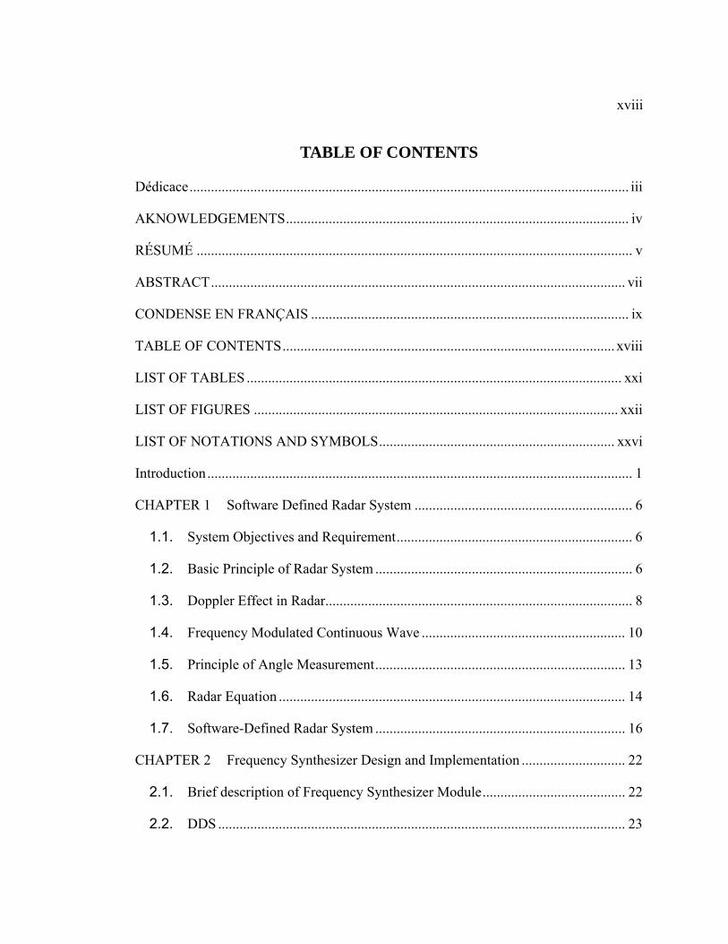
TABLE OF CONTENTS
Dédicace ........................................................................................................................... iii
AKNOWLEDGEMENTS ................................................................................................ iv
RÉSUMÉ .......................................................................................................................... v
ABSTRACT .................................................................................................................... vii
CONDENSE EN FRANÇAIS ......................................................................................... ix
TABLE OF CONTENTS ............................................................................................. xviii
LIST OF TABLES ......................................................................................................... xxi
LIST OF FIGURES ...................................................................................................... xxii
LIST OF NOTATIONS AND SYMBOLS .................................................................. xxvi
Introduction ....................................................................................................................... 1
CHAPTER 1 Software Defined Radar System ............................................................. 6
1.1. System Objectives and Requirement .................................................................. 6
1.2. Basic Principle of Radar System ........................................................................ 6
1.3. Doppler Effect in Radar...................................................................................... 8
1.4. Frequency Modulated Continuous Wave ......................................................... 10
1.5. Principle of Angle Measurement ...................................................................... 13
1.6. Radar Equation ................................................................................................. 14
1.7. Software-Defined Radar System ...................................................................... 16
CHAPTER 2 Frequency Synthesizer Design and Implementation ............................. 22
2.1. Brief description of Frequency Synthesizer Module ........................................ 22
2.2. DDS .................................................................................................................. 23
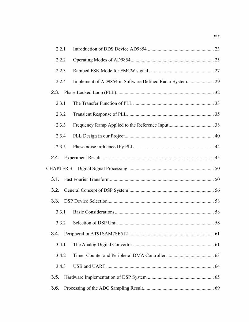
xix
2.2.1 Introduction of DDS Device AD9854 ...................................................... 23
2.2.2 Operating Modes of AD9854 .................................................................... 25
2.2.3 Ramped FSK Mode for FMCW signal ..................................................... 27
2.2.4 Implement of AD9854 in Software Defined Radar System...................... 29
2.3. Phase Locked Loop (PLL)................................................................................ 32
2.3.1 The Transfer Function of PLL .................................................................. 33
2.3.2 Transient Response of PLL ....................................................................... 35
2.3.3 Frequency Ramp Applied to the Reference Input ..................................... 38
2.3.4 PLL Design in our Project......................................................................... 40
2.3.5 Phase noise influenced by PLL ................................................................. 44
2.4. Experiment Result ............................................................................................ 45
CHAPTER 3 Digital Signal Processing ...................................................................... 50
3.1. Fast Fourier Transform ..................................................................................... 50
3.2. General Concept of DSP System ...................................................................... 56
3.3. DSP Device Selection....................................................................................... 58
3.3.1 Basic Considerations ................................................................................. 58
3.3.2 Selection of DSP Unit ............................................................................... 58
3.4. Peripheral in AT91SAM7SE512 ...................................................................... 61
3.4.1 The Analog Digital Convertor .................................................................. 61
3.4.2 Timer Counter and Peripheral DMA Controller ....................................... 63
3.4.3 USB and UART ........................................................................................ 64
3.5. Hardware Implementation of DSP System ...................................................... 65
3.6. Processing of the ADC Sampling Result.......................................................... 69
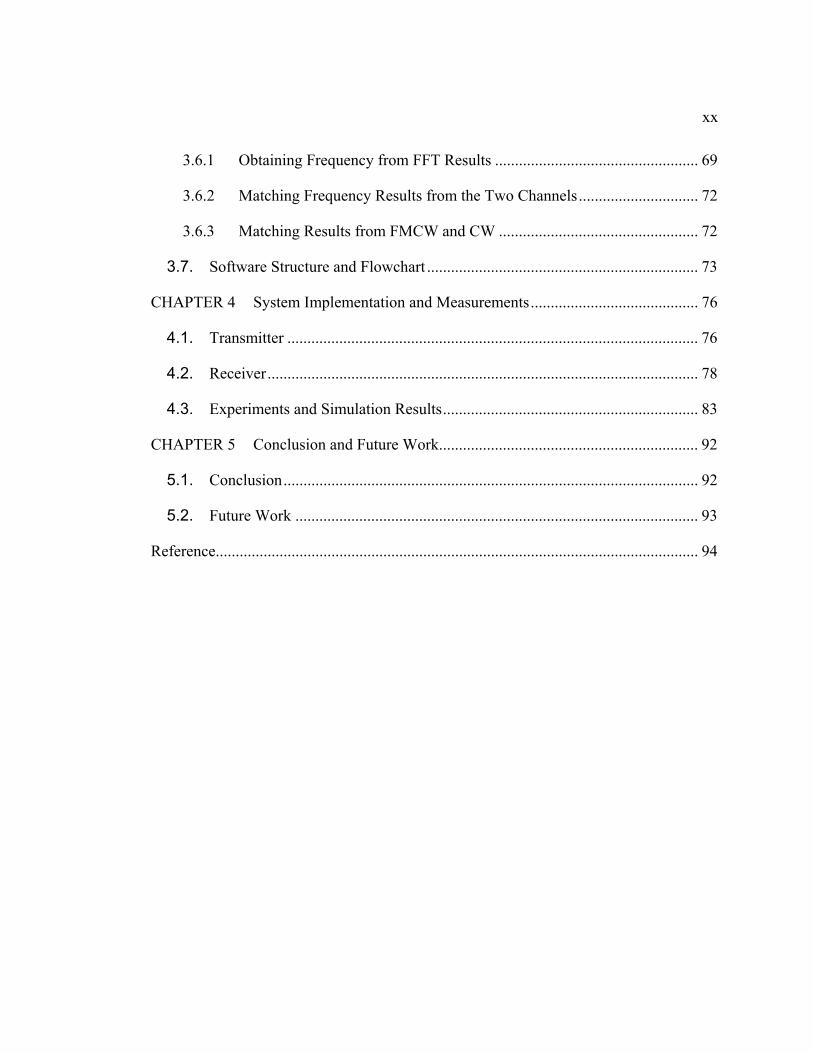
xx
3.6.1 Obtaining Frequency from FFT Results ................................................... 69
3.6.2 Matching Frequency Results from the Two Channels .............................. 72
3.6.3 Matching Results from FMCW and CW .................................................. 72
3.7. Software Structure and Flowchart .................................................................... 73
CHAPTER 4 System Implementation and Measurements .......................................... 76
4.1. Transmitter ....................................................................................................... 76
4.2. Receiver ............................................................................................................ 78
4.3. Experiments and Simulation Results ................................................................ 83
CHAPTER 5 Conclusion and Future Work................................................................. 92
5.1. Conclusion ........................................................................................................ 92
5.2. Future Work ..................................................................................................... 93
Reference......................................................................................................................... 94
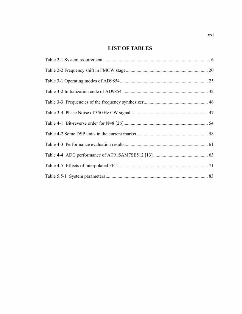
xxi
LIST OF TABLES
Table 2-1 System requirement .......................................................................................... 6
Table 2-2 Frequency shift in FMCW stage ..................................................................... 20
Table 3-1 Operating modes of AD9854 .......................................................................... 25
Table 3-2 Initialization code of AD9854 ........................................................................ 32
Table 3-3 Frequencies of the frequency synthesizer ...................................................... 46
Table 3-4 Phase Noise of 35GHz CW signal ................................................................. 47
Table 4-1 Bit-reverse order for N=8 [26] ....................................................................... 54
Table 4-2 Some DSP units in the current market ............................................................ 58
Table 4-3 Performance evaluation results ...................................................................... 61
Table 4-4 ADC performance of AT91SAM7SE512 [13] .............................................. 63
Table 4-5 Effects of interpolated FFT ............................................................................ 71
Table 5.5-1 System parameters ...................................................................................... 83
xxii
LIST OF FIGURES
Figure 1.1 Structure of an SIW slot array antenna ........................................................... 2
Figure 1.2 Block diagram of the proposed system ........................................................... 4
Figure 2.1 Two steps of radar operation ........................................................................... 7
Figure 2.2 Example of the upcoming vehicle ................................................................... 8
Figure 2.3 Linear FMCW waveform .............................................................................. 11
Figure 2.4 Principle of FMCW radar system ................................................................. 11
Figure 2.5 Angle measurement with phase difference ................................................... 14
Figure 2.6 Radar equation for transmission ................................................................... 15
Figure 2.7 Diagram of the proposed radar system .......................................................... 17
Figure 2.8. Combination of CW and FMCW ................................................................. 20
Figure 3.1 Diagram of Frequency Synthesizer. .............................................................. 22
Figure 3.2 Diagram of DDS operating principle ............................................................ 23
Figure 3.3 Function block diagram of AD9854 [11] ..................................................... 24
Figure 3.4 Single tone mode .......................................................................................... 25
Figure 3.5 Unramped FSK function [11] ....................................................................... 26
Figure 3.6 Example of chirp mode [11] ........................................................................ 27
Figure 3.7 Block diagram of ramped FSK function [11] ............................................... 28
Figure 3.8 An example of ramped FSK function [11] ................................................... 28
Figure 3.9 Ramped FSK mode for FMCW/CW waveform generation. ........................ 29
Figure 3.10 AD9854 circuit. .......................................................................................... 30
Figure 3.11 Filter for DDS output in ADS ...................................................................... 31
Figure 3.12 Simulation results of our DDS low pass filter ............................................. 31
xxiii
Figure 3.13 Block diagram of PLL ................................................................................. 33
Figure 3.14 Active PI filter ............................................................................................. 34
Figure 3.15. Bode diagram of the phase-transfer function ( )H jω of PLL. ................. 36
Figure 3.16. Simulation mode1 of PLL transient response with Simulink ..................... 37
Figure 3.17 Input of the 2nd order system ...................................................................... 37
Figure 3.18 Dynamic responses of the 2nd order system ................................................ 38
Figure 3.19. Function block diagram of AD4108 [12] .................................................. 40
Figure 3.20 PLL design model using AD4108 in ADIsimPLL ..................................... 41
Figure 3.21 Open and closed loop gain given by ADIsimPLL ....................................... 41
Figure 3.22 Simulation model of PLL in Simulink of Matlab ....................................... 42
Figure 3.23 Completely frequency response of PLL by using Simulink ........................ 43
Figure 3.24 Definition of phase noise spectrum [30] ..................................................... 44
Figure 3.25 Diagram of frequency synthesizer module ................................................. 46
Figure 3.26 Measured VCO modulation voltage signal................................................. 47
Figure 3.27 Frequency spectrum of CW signal ............................................................. 48
Figure 3.28 Frequency spectrum of FMCW signal. ........................................................ 49
Figure 4.1 Three stages in the computation of an N = 8-point DFT [26] ...................... 53
Figure 4.2 Basic butterfly computation [26] .................................................................. 53
Figure 4.3 C code for radix-2 FFT ................................................................................. 55
Figure 4.4 Basic function block diagram of a general DSP ........................................... 57
Figure 4.5 Function block diagram of AT91SAM7SExxx ............................................ 60
Figure 4.6 Function block diagram of ADC [13] ........................................................... 62
Figure 4.7 Relationship between ADC, Timer, PDC and memory ................................ 63
xxiv
Figure 4.8 The architecture of the DSP system.............................................................. 65
Figure 4.9 AT91 and SDRAM ........................................................................................ 67
Figure 4.10 IO extension for display ............................................................................. 68
Figure 4.11 IO extension for frequency synthesizer ...................................................... 68
Figure 4.12 Signal containing 3 components of different frequencies. ......................... 69
Figure 4.13 FFT results of the signal containing 3 frequency components ................... 70
Figure 4.14 Using Interpolated FFT............................................................................... 71
Figure 4.15 Software Structure ...................................................................................... 74
Figure 4.16 Whole software flowchart........................................................................... 74
Figure 4.17 Algorithm flowchart ................................................................................... 75
Figure 5.1 Transceiver module ...................................................................................... 77
Figure 5.2 Photo of the antenna ..................................................................................... 77
Figure 5.3 Measured antenna return loss ....................................................................... 78
Figure 5.4 Measured radiation pattern of antenna .......................................................... 78
Figure 5.5 Receiver Module ........................................................................................... 79
Figure 5.6 Filter and amplifier for the IF signal............................................................. 82
Figure 5.7 Simulated results of the filter and amplifier for IF ....................................... 83
Figure 5.8 Received power by radar vs. distance of target ............................................ 84
Figure 5.9 Final realized radar system ........................................................................... 85
Figure 5.10 Noise record ................................................................................................ 86
Figure 5.11 Simulation: angle measurement ambiguity ................................................ 86
Figure 5.12 Simulated noise’s influence on angle measurement ................................... 88
Figure 5.13 Angle measurement pattern ........................................................................ 89

xxv
Figure 5.14 Angle measurement results ......................................................................... 89
Figure 5.15 Distance measurement results..................................................................... 90
Figure 5.16 Experimental tests on highway and the results ........................................... 91
xxvi
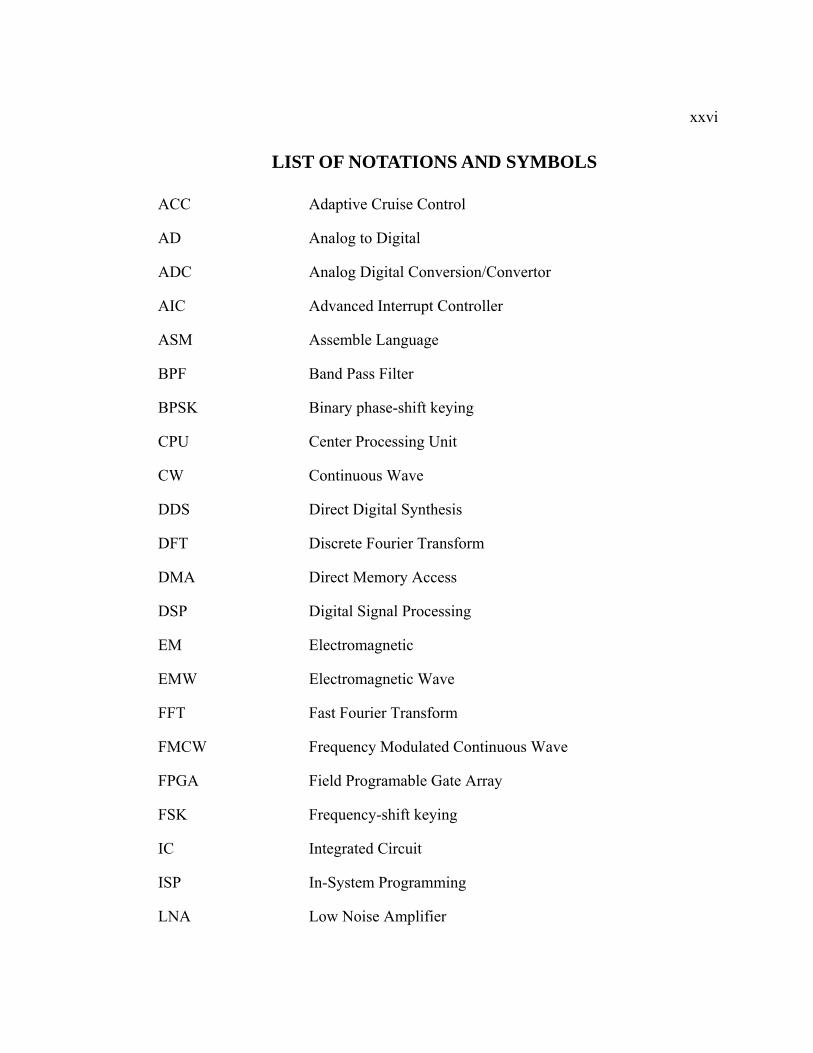
LIST OF NOTATIONS AND SYMBOLS
ACC Adaptive Cruise Control
AD Analog to Digital
ADC Analog Digital Conversion/Convertor
AIC Advanced Interrupt Controller
ASM Assemble Language
BPF Band Pass Filter
BPSK Binary phase-shift keying
CPU Center Processing Unit
CW Continuous Wave
DDS Direct Digital Synthesis
DFT Discrete Fourier Transform
DMA Direct Memory Access
DSP Digital Signal Processing
EM Electromagnetic
EMW Electromagnetic Wave
FFT Fast Fourier Transform
FMCW Frequency Modulated Continuous Wave
FPGA Field Programable Gate Array
FSK Frequency-shift keying
IC Integrated Circuit
ISP In-System Programming
LNA Low Noise Amplifier
xxvii
LPF Low Pass Filter
MCU Micro-Controller Unit
MIPS Million Instructions Per Second
PA Power Amplifier
PC Personal Computer
PDC Peripheral DMA Controller
PLL Phase-Locked Loop
PnP Plug and Play
SDR Software-Defined Radio
SIC Substrated Integrated Circuit
SIW Substrate Integrated Waveguide
UART Universal Asynchronous Receiver/Transmitter
UDP USB Device Port
USB Universal Serial Bus
VCO Voltage Controlled Oscillator
1
INTRODUCTION
With the continuous development of integrated circuits and wireless communication
technologies, radar applications are becoming ubiquitous. Although radar technologies
have intensively been investigated for more than a half century, most practical radar
implementations can only be used for specific applications, such as collision avoidance or
adaptive cruise control (ACC) functions in transportation systems or security applications
in both military and civil sectors. Moreover, radar technologies have progressed
enormously for defense applications but they are still not well prepared and developed for
commercial applications [2].
With the unprecedented advancement of digital radio and software technology, the
software-defined radio (SDR) technique was proposed and developed [4]. More and
more analog radio systems have been replaced by digital radio systems of various kinds.
On the other hand, programmable hardware modules have vastly been used in digital
radio systems at different functional levels. One of the objectives of using the SDR
technology is to take advantages of these programmable hardware modules and build up
flexible platforms based on software-defined radio system [4]. In the framework of a
software-defined technique, conventional radar techniques have also been moved towards
more and more digitized functional modules. Software-defined radar system platform
was developed by one previous thesis work in our group [2] [3]. With this new concept,
certain shortcomings of traditional radar system are resolved in some way. However, the
proposed system was only implemented with discrete devices and the parameter
measurement was only done in the laboratory environment.
It is well known that most of the radar devices and systems are directly conceived from
conventional architectures of the early version of military radars, which have a number of
problems [2]. First of all, an obvious drawback is their bulky size caused by a large
antenna which is also not easy to fabricate. The second problem is that most of them were
developed only for specific applications, and therefore there is a lack of flexibility. The
2
third shortcoming is that most radar systems are associated with a high cost and/or with an
inflexible function.
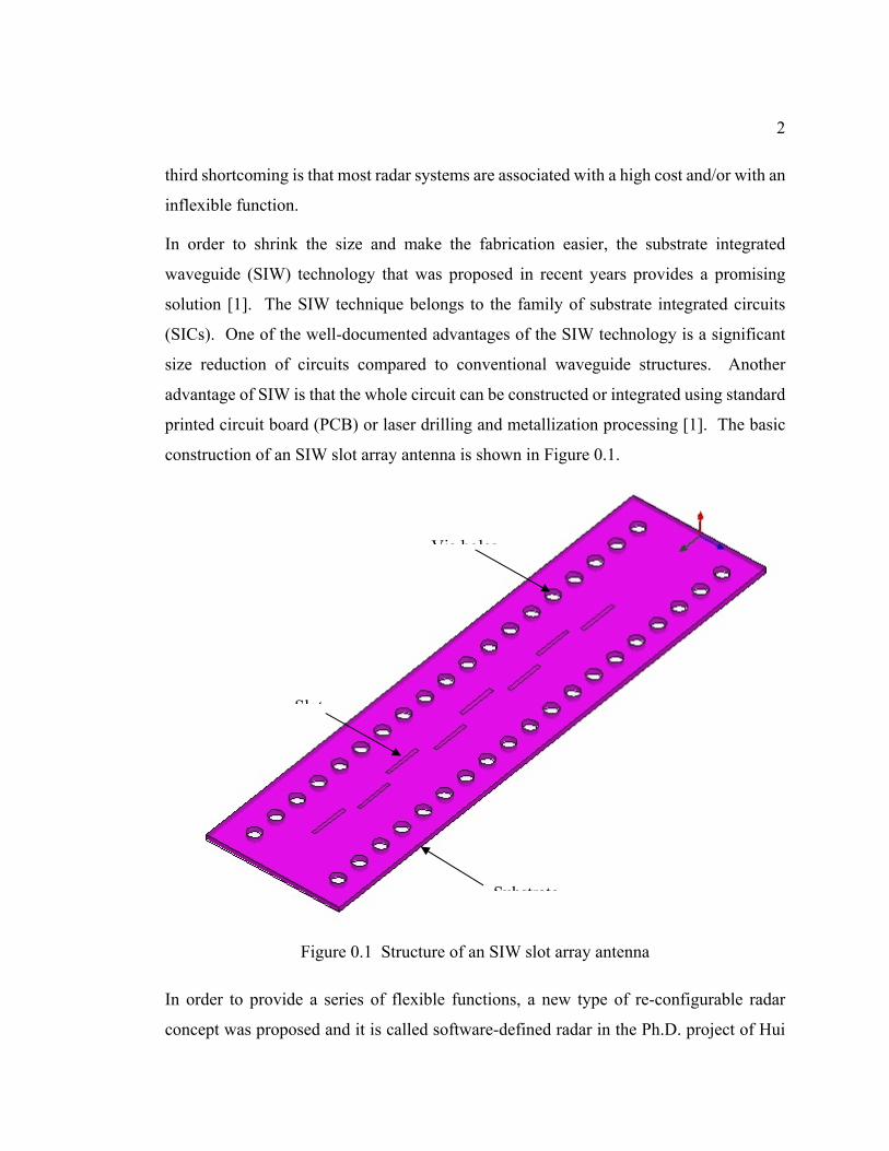
In order to shrink the size and make the fabrication easier, the substrate integrated
waveguide (SIW) technology that was proposed in recent years provides a promising
solution [1]. The SIW technique belongs to the family of substrate integrated circuits
(SICs). One of the well-documented advantages of the SIW technology is a significant
size reduction of circuits compared to conventional waveguide structures. Another
advantage of SIW is that the whole circuit can be constructed or integrated using standard
printed circuit board (PCB) or laser drilling and metallization processing [1]. The basic
construction of an SIW slot array antenna is shown in Figure 0.1.
Figure 0.1 Structure of an SIW slot array antenna
In order to provide a series of flexible functions, a new type of re-configurable radar
concept was proposed and it is called software-defined radar in the Ph.D. project of Hui
Via holes
Substrate
Slot
3
Zhang. The distinct feature of this software-defined radar is its flexibility of software
reconfigurable frequency synthesizer, front-end, system architecture and powerful digital
signal processing system. Generally speaking, the software-defined radar is a kind of
universal radar platform, within which, a flexible signal generation technique is realized
based on the clock or reference oscillator input together with a software configurable
capability.
Finally, the balance between cost and performance is achieved by adopting a number of
technologies. In the presented system, conventional waveguide antennas are replaced by
SIW antennas, and this not only reduces the whole size, but also decreases the fabricating
cost due to a simplified PCB craftwork. Moreover, with the help of the reconfigurable
transceiver and digital signal processing (DSP) system, the performances and
functionalities of the radar prototype are improved. Conventional radars realized at low
cost only have limited functions of parameter measurements such as the sole velocity
measurement, but the range and angle measurements are generally excluded. By
combining a flexible synthesizer with advanced DSP technique, software-defined radars
can provide an opportunity to implement multiple functionalities at low cost.
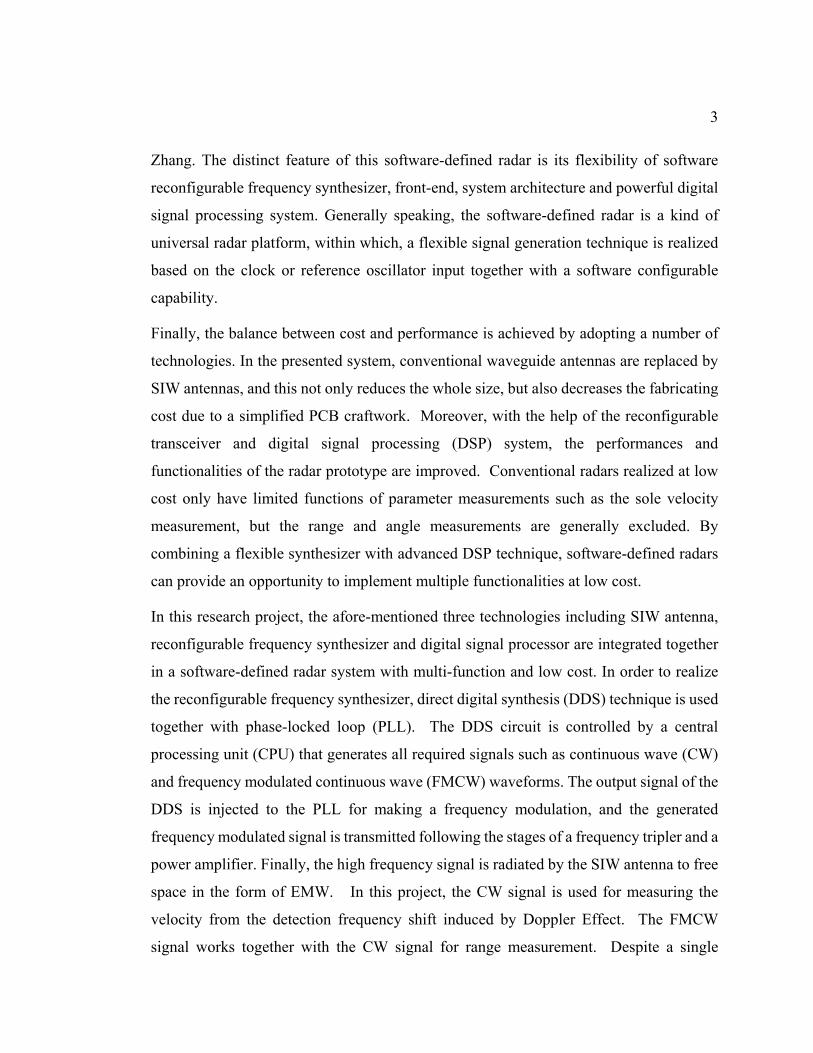
In this research project, the afore-mentioned three technologies including SIW antenna,
reconfigurable frequency synthesizer and digital signal processor are integrated together
in a software-defined radar system with multi-function and low cost. In order to realize
the reconfigurable frequency synthesizer, direct digital synthesis (DDS) technique is used
together with phase-locked loop (PLL). The DDS circuit is controlled by a central
processing unit (CPU) that generates all required signals such as continuous wave (CW)
and frequency modulated continuous wave (FMCW) waveforms. The output signal of the
DDS is injected to the PLL for making a frequency modulation, and the generated
frequency modulated signal is transmitted following the stages of a frequency tripler and a
power amplifier. Finally, the high frequency signal is radiated by the SIW antenna to free
space in the form of EMW. In this project, the CW signal is used for measuring the
velocity from the detection frequency shift induced by Doppler Effect. The FMCW
signal works together with the CW signal for range measurement. Despite a single
4
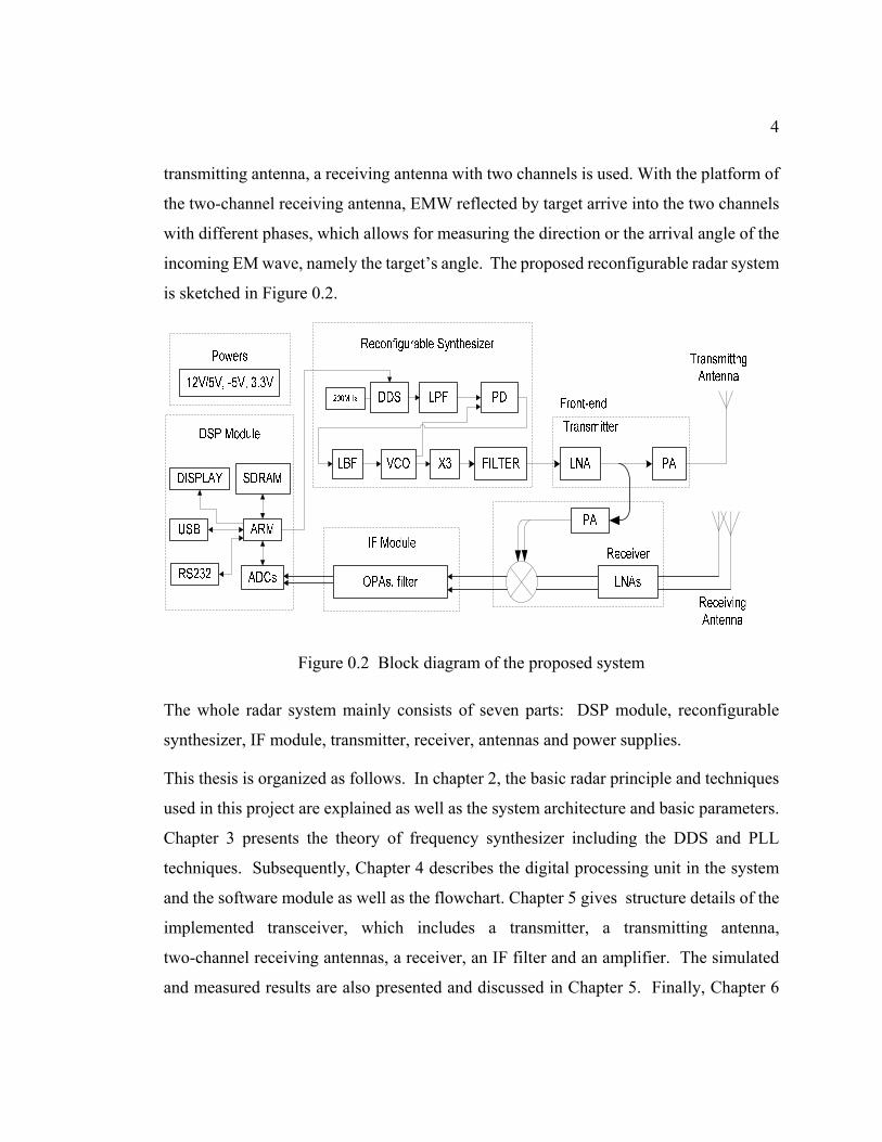
transmitting antenna, a receiving antenna with two channels is used. With the platform of
the two-channel receiving antenna, EMW reflected by target arrive into the two channels
with different phases, which allows for measuring the direction or the arrival angle of the
incoming EM wave, namely the target’s angle. The proposed reconfigurable radar system
is sketched in Figure 0.2.
Figure 0.2 Block diagram of the proposed system
The whole radar system mainly consists of seven parts: DSP module, reconfigurable
synthesizer, IF module, transmitter, receiver, antennas and power supplies.
This thesis is organized as follows. In chapter 2, the basic radar principle and techniques
used in this project are explained as well as the system architecture and basic parameters.
Chapter 3 presents the theory of frequency synthesizer including the DDS and PLL
techniques. Subsequently, Chapter 4 describes the digital processing unit in the system
and the software module as well as the flowchart. Chapter 5 gives structure details of the
implemented transceiver, which includes a transmitter, a transmitting antenna,
two-channel receiving antennas, a receiver, an IF filter and an amplifier. The simulated
and measured results are also presented and discussed in Chapter 5. Finally, Chapter 6

5
concludes this project and provides future research directions in connection with this
project.
6
CHAPTER 1 SOFTWARE DEFINED RADAR SYSTEM
1.1. System Objectives and Requirement
Like any radar system, the software-defined radar system is used to actively position the
targets with measuring the parameters of targets including velocity rang and angle. The
measurement result should meet the basic accuracy requirement shown in Table 1-1.
Table 1-1 System requirement
Items Value
RF frequency: 35GHz
Waveform type CW and FMCW
Measurement speed > 10 times per second
ADC sample frequency > 40kSPS (Sample per second)
Velocity error < 1 km/h
Range error < 1 m
Angle error < 1 degree
1.2. Basic Principle of Radar System
Generally speaking, a complete radar operation consists of two steps, which are shown in
Figure 1.1. Figure 1.1a shows the first step which is the transmitting phase and Figure
1.1b presents the second step which is the receiving phase. In both figures, “TL” means
microwave transmission line.
During the first step (transmitting phase), a transmitter produces a microwave signal
which is fed into an antenna at the end of the front-end transmission. Then, the microwave
signal is radiated by the antenna to the surrounding space in the form of a propagating
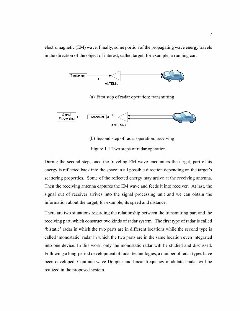
7
electromagnetic (EM) wave. Finally, some portion of the propagating wave energy travels
in the direction of the object of interest, called target, for example, a running car.
(a) First step of radar operation: transmitting
(b) Second step of radar operation: receiving
Figure 1.1 Two steps of radar operation
During the second step, once the traveling EM wave encounters the target, part of its
energy is reflected back into the space in all possible direction depending on the target’s
scattering properties. Some of the reflected energy may arrive at the receiving antenna.
Then the receiving antenna captures the EM wave and feeds it into receiver. At last, the
signal out of receiver arrives into the signal processing unit and we can obtain the
information about the target, for example, its speed and distance.
There are two situations regarding the relationship between the transmitting part and the
receiving part, which construct two kinds of radar system. The first type of radar is called
‘bistatic’ radar in which the two parts are in different locations while the second type is
called ‘monostatic’ radar in which the two parts are in the same location even integrated
into one device. In this work, only the monostatic radar will be studied and discussed.
Following a long-period development of radar technologies, a number of radar types have
been developed. Continue wave Doppler and linear frequency modulated radar will be
realized in the proposed system.
8
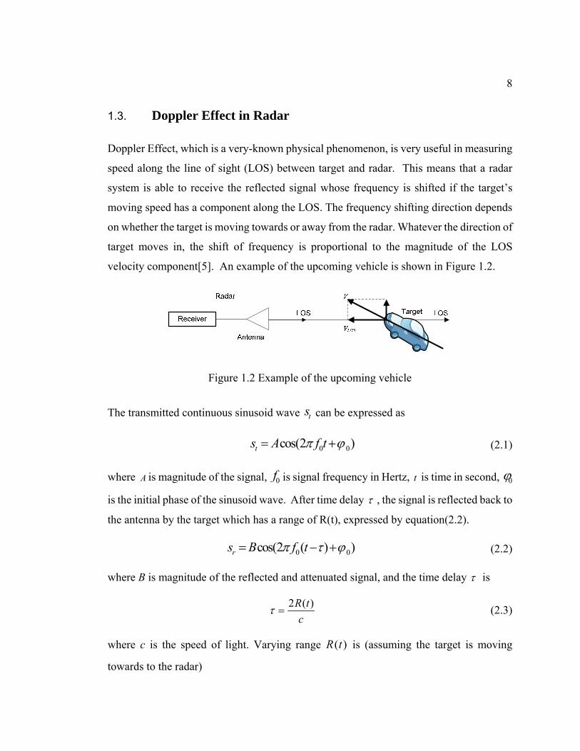
1.3. Doppler Effect in Radar
Doppler Effect, which is a very-known physical phenomenon, is very useful in measuring
speed along the line of sight (LOS) between target and radar. This means that a radar
system is able to receive the reflected signal whose frequency is shifted if the target’s
moving speed has a component along the LOS. The frequency shifting direction depends
on whether the target is moving towards or away from the radar. Whatever the direction of
target moves in, the shift of frequency is proportional to the magnitude of the LOS
velocity component[5]. An example of the upcoming vehicle is shown in Figure 1.2.
Figure 1.2 Example of the upcoming vehicle
The transmitted continuous sinusoid wave ts can be expressed as
0 0cos(2 )ts A f tπ ϕ= + (2.1)
where A is magnitude of the signal, 0f is signal frequency in Hertz, t is time in second, 0ϕ is the initial phase of the sinusoid wave. After time delay τ , the signal is reflected back to
the antenna by the target which has a range of R(t), expressed by equation(2.2).
0 0cos(2 ( ) )rs B f tπ τ ϕ= − + (2.2)
where B is magnitude of the reflected and attenuated signal, and the time delay τ is
2 ( )R tc
τ = (2.3)
where c is the speed of light. Varying range ( )R t is (assuming the target is moving
towards to the radar)
9
0( ) LOSR t R v t= − (2.4)
where 0R is the initial range at time t=0, LOSv is the velocity component of LOS. By
substituting (2.3) and (2.4) into equation (2.2) we can obtain
00 0
2( )cos(2 ( ) )LOSr
R v ts B f tc
π ϕ−= − + (2.5)
This can be simplified to
0cos(2 ( ) )r d rs B f f tπ ϕ= + + (2.6)
where phase rϕ is
0 00
4r
f Rc
πϕ ϕ= − (2.7)
and frequency shift df is
02 LOS
dvf fc
= (2.8)
This df is the Doppler frequency shift which is produced because the target has an LOS
velocity component. Therefore, the speed of the target moving toward the antenna vlos can
be calculated from measuring the Doppler frequency:
02d
LOSf cv
f= (2.9)
Since the velocity calculation depends on the measured Doppler frequency shift, the
accuracy of velocity is determined by the accuracy of frequency measurement. The
velocity resolution can be computed as,
,
02d res
res
f cv
f= (2.10)
10
where resv is velocity resolution, ,d resf is Doppler frequency resolution. At the same time,
,d resf is a reciprocal parameter of measurement period T, namely, we have
02rescvf T
= (2.11)
Once the frequency of the transmitted signal is given, the velocity measurement
resolution is determined by measurement period T.
Due to the fact that velocity vlos has its direction, towards or away from the radar
reference, the Doppler shift frequency gets its own positive or negative direction. By
determining whether the Doppler shift frequency is positive or negative, the radar can
detect the moving direction of the target.
1.4. Frequency Modulated Continuous Wave
Besides the velocity measurement, range measurement is another issue in the
development of radar technology. One way to measure the range is using
pulsed-modulated radar. Pulsed-modulated radar measures the range by measuring the
traveling time of a very short pulse between the radar and the target. Since it is not easy to
realize a very narrow pulse width, it is difficult to yield a high resolution of range. As a
substitute, the frequency modulated continuous wave can be employed in radar system in
order to obtain a higher resolution in range measurement. Frequency modulated
continuous wave also features a low power level, which allows using solid state
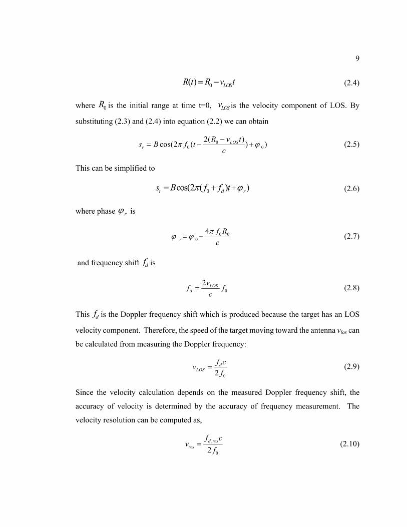
microwave circuits. Figure 1.3 shows an example of linear FMCW waveform.
The linear FMCW waveform shown in Figure 1.3 can be expressed by
0cos[2 ( ) ]t rs f f t tπ= + (2.12)
11
where 0f is the frequency of signal at time 0t = , rf is the frequency slew rate. In this
case rs is a positive constant value. If rs is a negative constant value, the frequency will
decrease over time.
Figure 1.3 Linear FMCW waveform
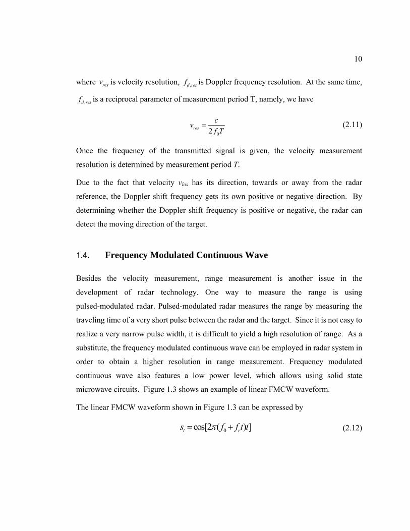
Figure 1.4 Principle of FMCW radar system
Figure 1.4 shows how the FMCW works in range measurement process. In Figure 1.4,
the solid black leaning line represents the transmitted signal’s frequency and the dash
green (maybe black or gray due to the printer) leaning line represents the frequency of
received signal which is reflected back by the target at position of range R to the radar.
Obviously, the received signal’s frequency is retarded by time delay ∆t according to the
time during the signal traveling from the radar to the target and returning from the target
to the radar, a total range is 2R.
12
As we can detect the frequency shift between the transmitted signal’s frequency and
received signal’s frequency, it is easy to obtain the traveling time of signal between the
radar and the target.
Observing Figure 1.4, we have the following relation
2 1
t Tf F F=
− (2.13)
Then the equation for the traveling time is:
2 1
Tt fF F
=−
(2.14)
where ∆t is the travelling time, T is the frequency scanning time from F1 to F2, f is the
frequency difference between the received and transmitted signals.
Finally, we can get the target range by
2t cR ×
=
(2.15)
namely,
2 12( )TcR f
F F=
− (2.16)
where R is the range between the radar and the target, c is the speed of light. The
resolution of measured range depends on the resolution of ∆f. The resolution of ∆f
depends on the scanning time T:
1resolutionf
T=
Then the resolution of range can be formulated by the following equation
13
2 12( )resolutioncR
F F=
− (2.17)
From Equation (2.17) we can see that the range resolution of FMCW system is decided by
the sweep bandwidth of the transmitted signal.
Similar to Doppler radar, FMCW radar is also able to collect multi-range information of
multi-target by distinguishing different frequency from one single signal.
All of the above discussions are made based on one assumption that the target is fixed on
its location without LOS velocity. If LOS velocity is present, the Doppler frequency shift
will be mixed in the receiving frequency, leading to the fact that ∆f includes not only the
range information but also the speed information. It is a challenge to separate them from
each other, especially when there are multiple targets in the detection range of the radar.
In our system, we combine the FMCW and CW platforms together in order to collect the
range information from FMCW signal without ambiguity.
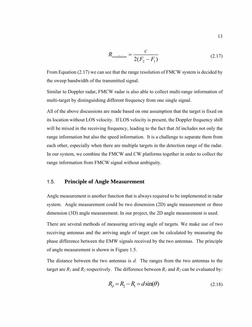
1.5. Principle of Angle Measurement
Angle measurement is another function that is always required to be implemented in radar
system. Angle measurement could be two dimension (2D) angle measurement or three
dimension (3D) angle measurement. In our project, the 2D angle measurement is used.
There are several methods of measuring arriving angle of targets. We make use of two
receiving antennas and the arriving angle of target can be calculated by measuring the
phase difference between the EMW signals received by the two antennas. The principle
of angle measurement is shown in Figure 1.5.
The distance between the two antennas is d. The ranges from the two antennas to the
target are R1 and R2 respectively. The difference between R1 and R2 can be evaluated by:
2 1 sin( )dR R R d θ= − = (2.18)
14
.
Figure 1.5 Angle measurement with phase difference
The measured phase difference between two received signals is related to Rd by
2 dd
Rπϕλ
= (2.19)
where λ is the wavelength of the transmitting signal. From (2.18) and(2.19), we can get
the arriving angle of the target by
0
arcsin arcsin arcsin2 2
d d dR cd d df
λϕ ϕθπ π
⎛ ⎞⎛ ⎞ ⎛ ⎞= = = ⎜ ⎟⎜ ⎟ ⎜ ⎟⎝ ⎠ ⎝ ⎠ ⎝ ⎠
(2.20)
where c is the speed of light in m/s, and 0f is the frequency of transmitting signal.
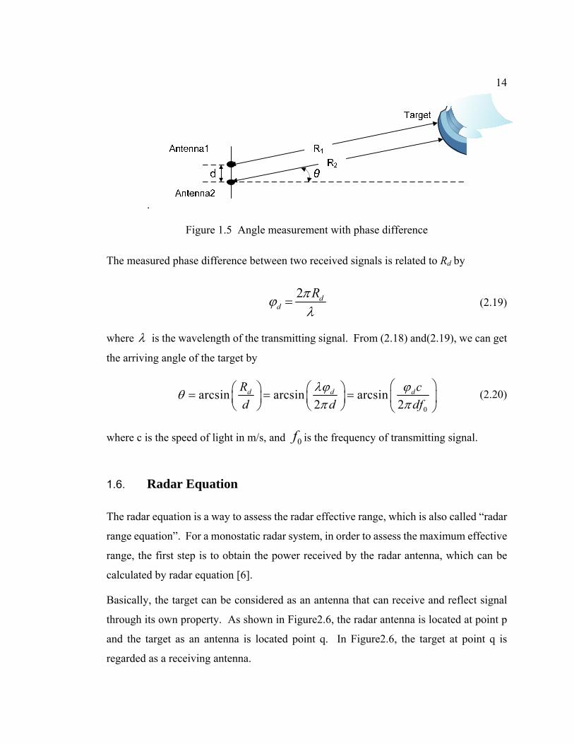
1.6. Radar Equation
The radar equation is a way to assess the radar effective range, which is also called “radar
range equation”. For a monostatic radar system, in order to assess the maximum effective
range, the first step is to obtain the power received by the radar antenna, which can be
calculated by radar equation [6].
Basically, the target can be considered as an antenna that can receive and reflect signal
through its own property. As shown in Figure2.6, the radar antenna is located at point p
and the target as an antenna is located point q. In Figure2.6, the target at point q is
regarded as a receiving antenna.
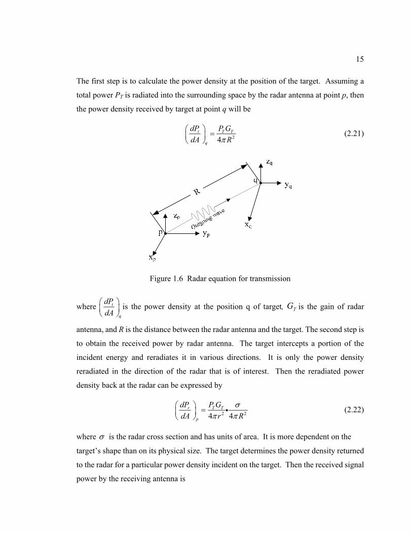
15
The first step is to calculate the power density at the position of the target. Assuming a
total power PT is radiated into the surrounding space by the radar antenna at point p, then
the power density received by target at point q will be
24t T T
q
dP P GdA Rπ
⎛ ⎞ =⎜ ⎟⎝ ⎠
(2.21)
Figure 1.6 Radar equation for transmission
where t
q
dPdA
⎛ ⎞⎜ ⎟⎝ ⎠
is the power density at the position q of target, TG is the gain of radar
antenna, and R is the distance between the radar antenna and the target. The second step is
to obtain the received power by radar antenna. The target intercepts a portion of the
incident energy and reradiates it in various directions. It is only the power density
reradiated in the direction of the radar that is of interest. Then the reradiated power
density back at the radar can be expressed by
2 24 4r T T
p
dP P GdA r R
σπ π
⎛ ⎞ =⎜ ⎟⎝ ⎠
i
(2.22)
where σ is the radar cross section and has units of area. It is more dependent on the
target’s shape than on its physical size. The target determines the power density returned
to the radar for a particular power density incident on the target. Then the received signal
power by the receiving antenna is
16
2 2 2 44 4 (4 )T T er T T
r e ep
P G AdP P GP A AdA R R R
σσπ π π
⎛ ⎞= = =⎜ ⎟⎝ ⎠
i i i ,
(2.23)
where eA is the effective area of the receiving antenna. According to antenna theory, the
relationship between the gain of antenna and the effective area is given by
2
4 eAG πλ
=
(2.24)
where G is the gain of antenna, λ is the wavelength of the signal. Substituting (2.24)
into(2.23), we get the final form of received power as
2
3 4(4 )T T R
rP G GP
Rλ σ
π= .
(2.25)
RG is the gain of receiving antenna. From equation (2.25), the maximum range of a
radar maxR can be calculated as
2
4max 3min(4 ) P
T T RP G GR λ σπ
= .
(2.26)
where the minP is the minimum power of detectable signal of the radar system.
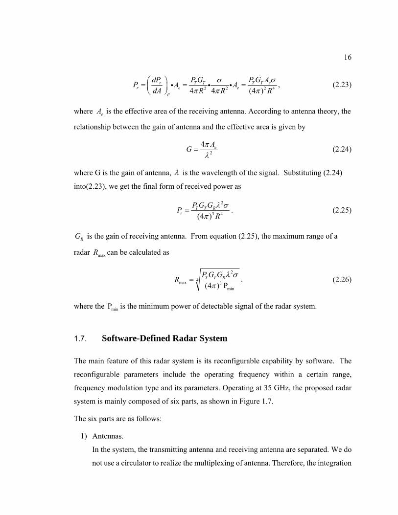
1.7. Software-Defined Radar System
The main feature of this radar system is its reconfigurable capability by software. The
reconfigurable parameters include the operating frequency within a certain range,
frequency modulation type and its parameters. Operating at 35 GHz, the proposed radar
system is mainly composed of six parts, as shown in Figure 1.7.
The six parts are as follows:
1) Antennas.
In the system, the transmitting antenna and receiving antenna are separated. We do
not use a circulator to realize the multiplexing of antenna. Therefore, the integration
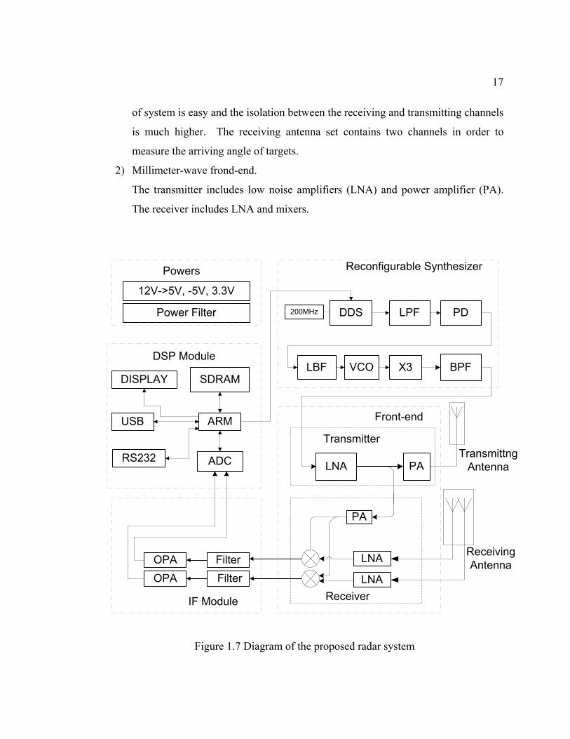
17
of system is easy and the isolation between the receiving and transmitting channels
is much higher. The receiving antenna set contains two channels in order to
measure the arriving angle of targets.
2) Millimeter-wave frond-end.
The transmitter includes low noise amplifiers (LNA) and power amplifier (PA).
The receiver includes LNA and mixers.
Front-end
Receiver
ReceivingAntenna
TransmittngAntennaLNA PA
BPF
DDS LPF PD
X3VCOLBFDSP Module
Reconfigurable Synthesizer
ADC
SDRAM
ARMUSB
RS232
DISPLAY
IF Module
Transmitter
Powers
12V->5V, -5V, 3.3V
PA
Filter
200MHzPower Filter
LNA
LNA
FilterOPAOPA
Figure 1.7 Diagram of the proposed radar system
18
3) Reconfigurable frequency synthesizer.
The frequency synthesizer module consists of DDS, PLL, voltage controlled
oscillator (VCO) and frequency tripler. The frequency synthesizer produces the
required waveform for CW and FMCW functions.
4) Intermediate frequency (IF) modules.
The IF module includes several amplifiers and band pass filters through which the
IF signal is filtered and amplified to a proper range of voltage and then drives the
analog-to-digital converter (ADC) embedded in DSP module.
5) Digital signal processing module with embedded analog to digital convertor;
This module converts the analog IF signal into digital signal and processes the
signal according to a digital signal processing algorithm. Moreover, this module
configures the reconfigurable frequency synthesizer and interacts with the user
interface.
6) Power module.
The power module includes several DC-DC converters, linear power regulators and
ripple suppression filters, which generate +5V, -5V, +3.3V powers for each part of
the radar system.
The main purpose of this project is to realize different radar functions within one single
hardware platform. The switching and combination of different radar functions are
realized by the software that controls the signal synthesizer and digital signal processing
parts. In our study, CW radar and FMCW radar functions are integrated. The CW function
can detect the speed information of targets and the FMCW function can detect the range
information of targets.
In order to realize small sized radar, our system works at 35.1 GHz. Therefore, the
antenna can be very compact. In addition, we implement the SIW into our antenna design,
which features low loss and planar form that can be made compatible with standard
printed circuit board (PCB) technology.
19
The linearity of the FMCW signal decides the accuracy of the range measurement. There
are several techniques for realizing a linear FMCW signal, such as PLL, triangular wave
modulated VCO, etc. We use DDS combined with PLL to realize an ideal linear FMCW
microwave signal. The microwave signal is then multiplied to millimeter-wave signal for
driving the transmitting stage and LO source.
The millimeter-wave front-end is integrated into several boards. The boards are packaged
into a single enclosure. The whole system is in the form of a planar structure. The receiver
is in a homodyne configuration, which is simple and presents phase noise coherent
features. The receiver has two identical channels. The two channels are connected with
two identical closely-spaced receiving antennas. Therefore, the arrival angle of the targets
can be detected for both CW and FMCW modes.
The IF signals are filtered and amplified before the ADC. The digitalized IF signals are
processed in the DSP system according to corresponding algorithms. In this study, fast
fourier transform (FFT) is the main algorithm for digital processing to evaluate the
spectrum information of the received IF signal. The speed, range, and arriving angle of the
targets are calculated in DSP. In addition, some software codes are created for
communication between DSP and computer as well as interface to the users.
The transmitted frequency of signal in CW mode is 35.1GHz. According to equation(2.8)
, the Doppler frequency for a speed range of 10km/h and 200 km/h is between 650Hz and
13 KHz.
With measurement period 50ms, the velocity resolution is
0
0.085 / 0.3 /2res
cv m s Km hf T
= = = (2.27)
The transmitted frequency of signal in FMCW mode is 35.1GHz~35.6GHz. The
bandwidth is 500MHz so the range resolution is
2 1
=0.3m2( )resolution
cRF F
=−
(2.28)
20
According to (2.16), the frequency measured for static target in a range between 1m and
100 m is from 66.6 Hz to 6.66KHz.
In real environment, the target cannot be static. Therefore, the Doppler frequency shift
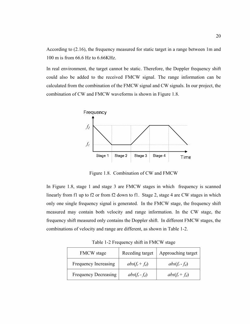
could also be added to the received FMCW signal. The range information can be
calculated from the combination of the FMCW signal and CW signals. In our project, the
combination of CW and FMCW waveforms is shown in Figure 1.8.
Figure 1.8. Combination of CW and FMCW
In Figure 1.8, stage 1 and stage 3 are FMCW stages in which frequency is scanned
linearly from f1 up to f2 or from f2 down to f1. Stage 2, stage 4 are CW stages in which
only one single frequency signal is generated. In the FMCW stage, the frequency shift
measured may contain both velocity and range information. In the CW stage, the
frequency shift measured only contains the Doppler shift. In different FMCW stages, the
combinations of velocity and range are different, as shown in Table 1-2.
Table 1-2 Frequency shift in FMCW stage
FMCW stage Receding target Approaching target
Frequency Increasing abs(fr + fd) abs(fr - fd)
Frequency Decreasing abs(fr - fd) abs(fr + fd)

21
In Table 1-2, fr is the frequency shift due to range, fd is Doppler shift due to velocity and
abs is the absolute value function.
22
CHAPTER 2 FREQUENCY SYNTHESIZER DESIGN AND
IMPLEMENTATION
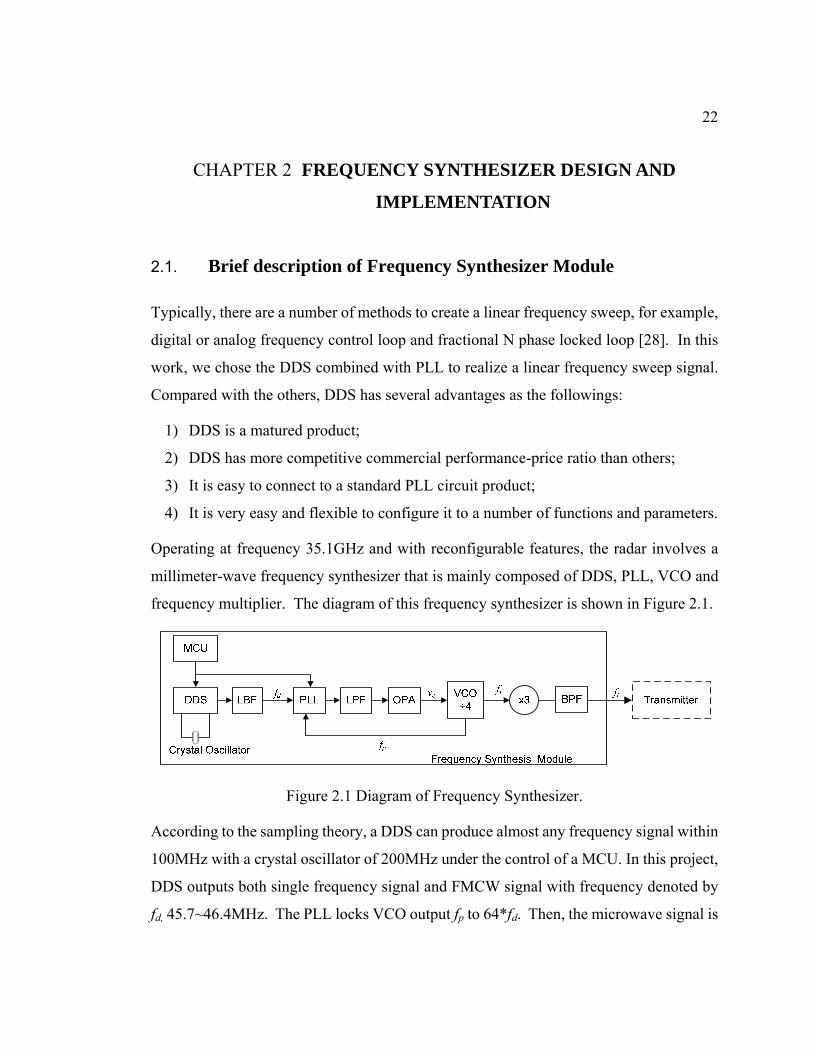
2.1. Brief description of Frequency Synthesizer Module
Typically, there are a number of methods to create a linear frequency sweep, for example,
digital or analog frequency control loop and fractional N phase locked loop [28]. In this
work, we chose the DDS combined with PLL to realize a linear frequency sweep signal.
Compared with the others, DDS has several advantages as the followings:
1) DDS is a matured product;
2) DDS has more competitive commercial performance-price ratio than others;
3) It is easy to connect to a standard PLL circuit product;
4) It is very easy and flexible to configure it to a number of functions and parameters.
Operating at frequency 35.1GHz and with reconfigurable features, the radar involves a
millimeter-wave frequency synthesizer that is mainly composed of DDS, PLL, VCO and
frequency multiplier. The diagram of this frequency synthesizer is shown in Figure 2.1.
Figure 2.1 Diagram of Frequency Synthesizer.
According to the sampling theory, a DDS can produce almost any frequency signal within
100MHz with a crystal oscillator of 200MHz under the control of a MCU. In this project,
DDS outputs both single frequency signal and FMCW signal with frequency denoted by
fd, 45.7~46.4MHz. The PLL locks VCO output fp to 64*fd. Then, the microwave signal is
23
multiplied by x3 frequency multiplier and we generate the transmitting signal with
frequency ft.
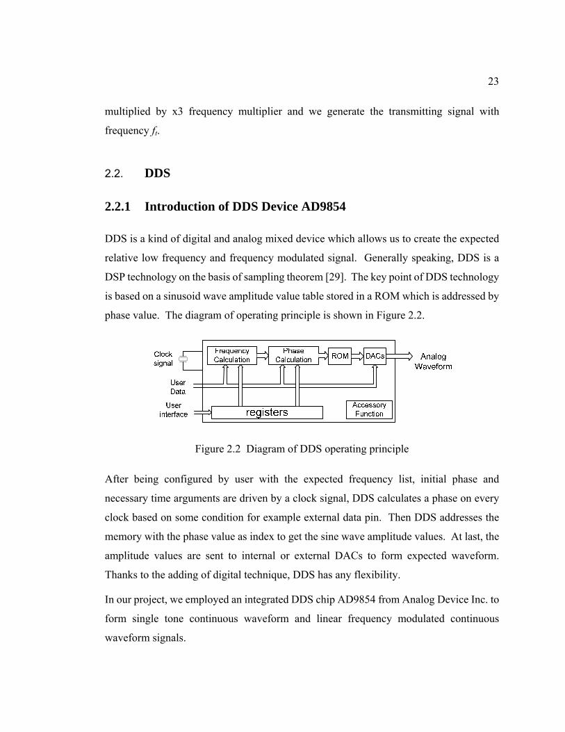
2.2. DDS
2.2.1 Introduction of DDS Device AD9854
DDS is a kind of digital and analog mixed device which allows us to create the expected
relative low frequency and frequency modulated signal. Generally speaking, DDS is a
DSP technology on the basis of sampling theorem [29]. The key point of DDS technology
is based on a sinusoid wave amplitude value table stored in a ROM which is addressed by
phase value. The diagram of operating principle is shown in Figure 2.2.
Figure 2.2 Diagram of DDS operating principle
After being configured by user with the expected frequency list, initial phase and
necessary time arguments are driven by a clock signal, DDS calculates a phase on every
clock based on some condition for example external data pin. Then DDS addresses the
memory with the phase value as index to get the sine wave amplitude values. At last, the
amplitude values are sent to internal or external DACs to form expected waveform.
Thanks to the adding of digital technique, DDS has any flexibility.
In our project, we employed an integrated DDS chip AD9854 from Analog Device Inc. to
form single tone continuous waveform and linear frequency modulated continuous
waveform signals.
24
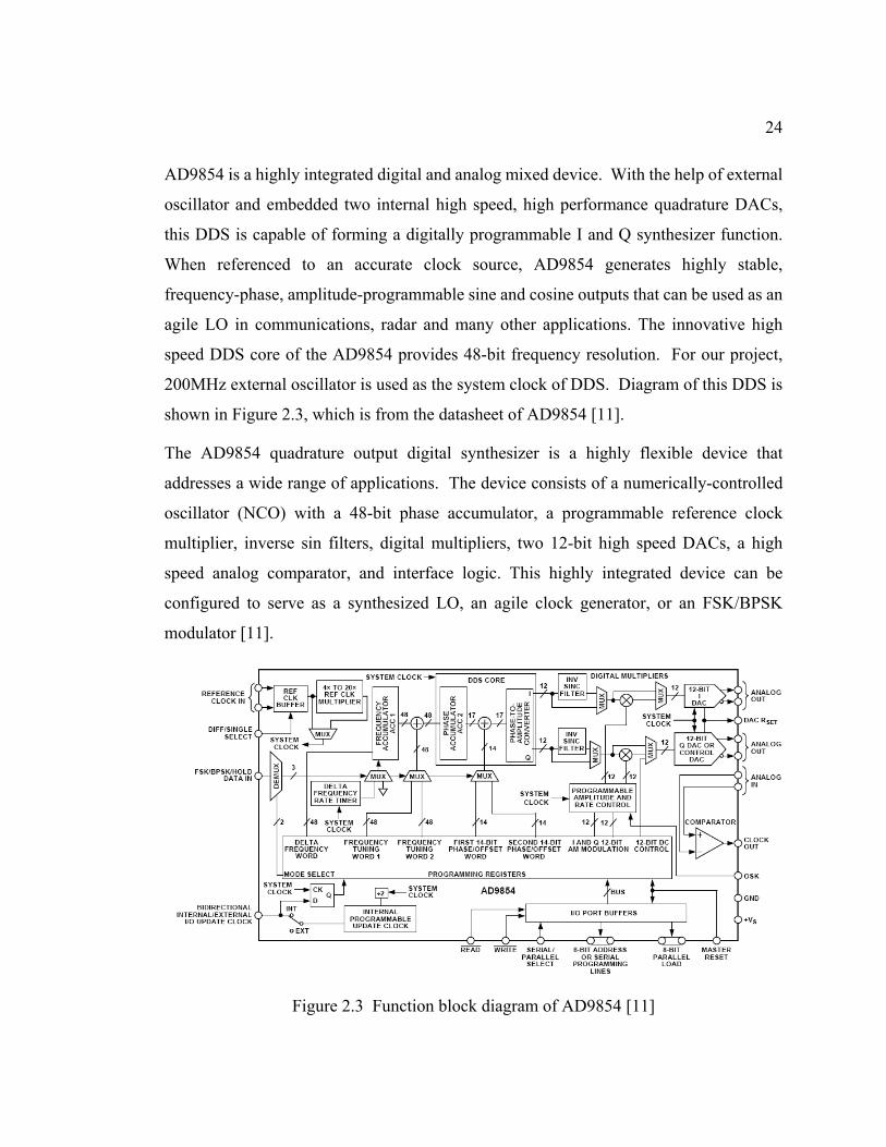
AD9854 is a highly integrated digital and analog mixed device. With the help of external
oscillator and embedded two internal high speed, high performance quadrature DACs,
this DDS is capable of forming a digitally programmable I and Q synthesizer function.
When referenced to an accurate clock source, AD9854 generates highly stable,
frequency-phase, amplitude-programmable sine and cosine outputs that can be used as an
agile LO in communications, radar and many other applications. The innovative high
speed DDS core of the AD9854 provides 48-bit frequency resolution. For our project,
200MHz external oscillator is used as the system clock of DDS. Diagram of this DDS is
shown in Figure 2.3, which is from the datasheet of AD9854 [11].
The AD9854 quadrature output digital synthesizer is a highly flexible device that
addresses a wide range of applications. The device consists of a numerically-controlled
oscillator (NCO) with a 48-bit phase accumulator, a programmable reference clock
multiplier, inverse sin filters, digital multipliers, two 12-bit high speed DACs, a high
speed analog comparator, and interface logic. This highly integrated device can be
configured to serve as a synthesized LO, an agile clock generator, or an FSK/BPSK
modulator [11].
Figure 2.3 Function block diagram of AD9854 [11]
25
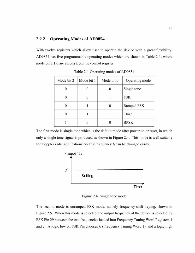
2.2.2 Operating Modes of AD9854
With twelve registers which allow user to operate the device with a great flexibility,
AD9854 has five programmable operating modes which are shown in Table 2-1, where
mode bit 2,1,0 are all bits from the control register.
Table 2-1 Operating modes of AD9854
Mode bit 2 Mode bit 1 Mode bit 0 Operating mode
0 0 0 Single tone
0 0 1 FSK
0 1 0 Ramped FSK
0 1 1 Chirp
1 0 0 BPSK
The first mode is single tone which is the default mode after power on or reset, in which
only a single tone signal is produced as shown in Figure 2.4. This mode is well suitable
for Doppler radar applications because frequency f1 can be changed easily.
Figure 2.4 Single tone mode
The second mode is unramped FSK mode, namely frequency-shift keying, shown in
Figure 2.5. When this mode is selected, the output frequency of the device is selected by
FSK Pin 29 between the two frequencies loaded into Frequency Tuning Word Registers 1
and 2. A logic low on FSK Pin chooses f1 (Frequency Tuning Word 1), and a logic high
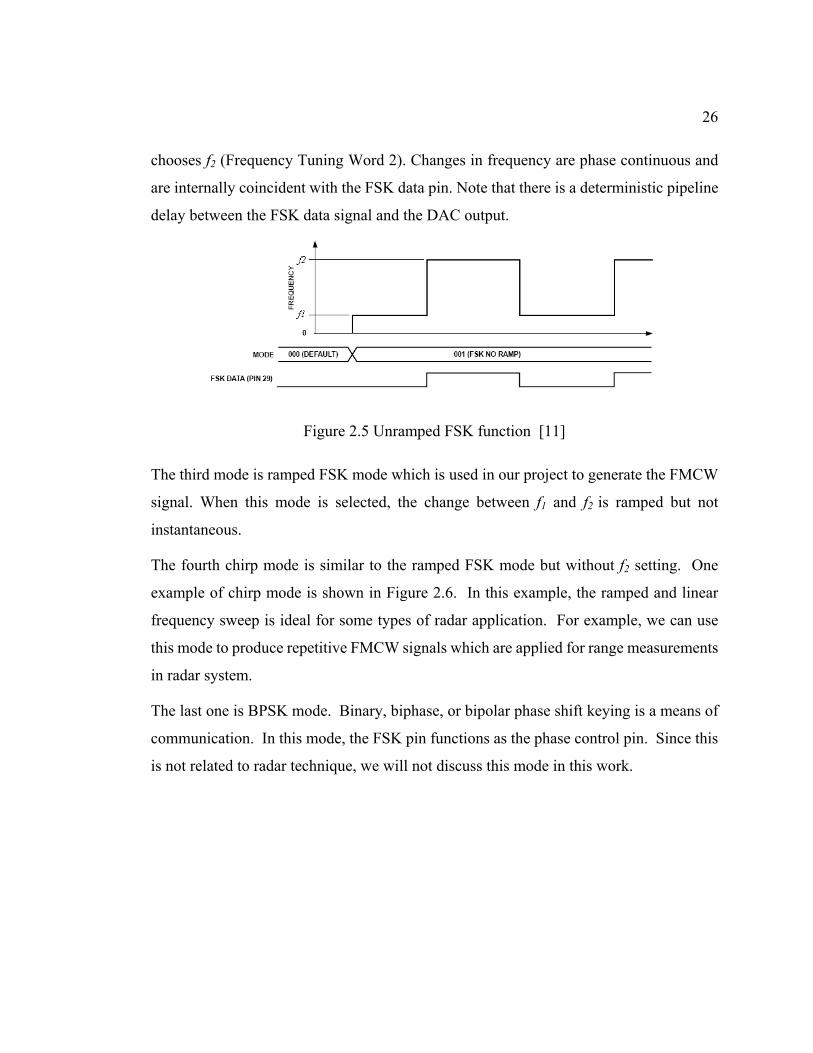
26
chooses f2 (Frequency Tuning Word 2). Changes in frequency are phase continuous and
are internally coincident with the FSK data pin. Note that there is a deterministic pipeline
delay between the FSK data signal and the DAC output.
Figure 2.5 Unramped FSK function [11]
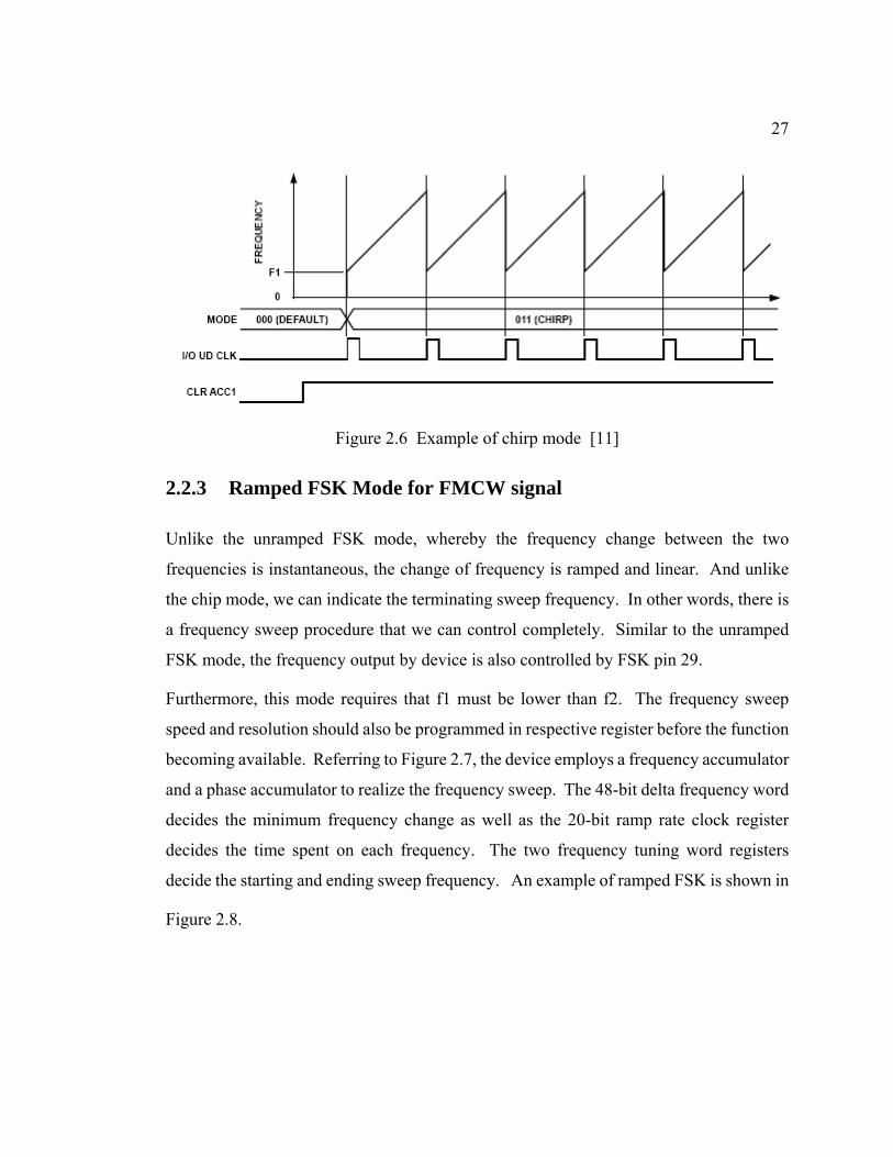
The third mode is ramped FSK mode which is used in our project to generate the FMCW
signal. When this mode is selected, the change between f1 and f2 is ramped but not
instantaneous.
The fourth chirp mode is similar to the ramped FSK mode but without f2 setting. One
example of chirp mode is shown in Figure 2.6. In this example, the ramped and linear
frequency sweep is ideal for some types of radar application. For example, we can use
this mode to produce repetitive FMCW signals which are applied for range measurements
in radar system.
The last one is BPSK mode. Binary, biphase, or bipolar phase shift keying is a means of
communication. In this mode, the FSK pin functions as the phase control pin. Since this
is not related to radar technique, we will not discuss this mode in this work.
27
Figure 2.6 Example of chirp mode [11]
2.2.3 Ramped FSK Mode for FMCW signal
Unlike the unramped FSK mode, whereby the frequency change between the two
frequencies is instantaneous, the change of frequency is ramped and linear. And unlike
the chip mode, we can indicate the terminating sweep frequency. In other words, there is
a frequency sweep procedure that we can control completely. Similar to the unramped
FSK mode, the frequency output by device is also controlled by FSK pin 29.
Furthermore, this mode requires that f1 must be lower than f2. The frequency sweep
speed and resolution should also be programmed in respective register before the function
becoming available. Referring to Figure 2.7, the device employs a frequency accumulator
and a phase accumulator to realize the frequency sweep. The 48-bit delta frequency word
decides the minimum frequency change as well as the 20-bit ramp rate clock register
decides the time spent on each frequency. The two frequency tuning word registers
decide the starting and ending sweep frequency. An example of ramped FSK is shown in
Figure 2.8.
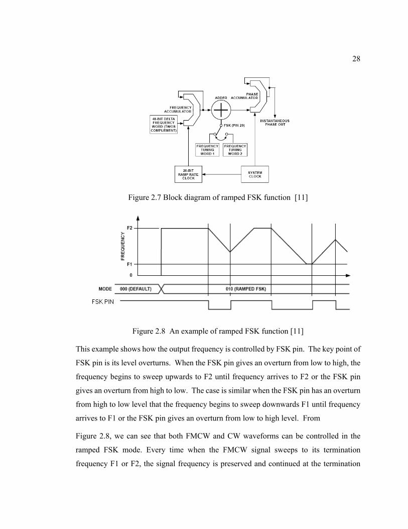
28
Figure 2.7 Block diagram of ramped FSK function [11]
Figure 2.8 An example of ramped FSK function [11]
This example shows how the output frequency is controlled by FSK pin. The key point of
FSK pin is its level overturns. When the FSK pin gives an overturn from low to high, the
frequency begins to sweep upwards to F2 until frequency arrives to F2 or the FSK pin
gives an overturn from high to low. The case is similar when the FSK pin has an overturn
from high to low level that the frequency begins to sweep downwards F1 until frequency
arrives to F1 or the FSK pin gives an overturn from low to high level. From
Figure 2.8, we can see that both FMCW and CW waveforms can be controlled in the
ramped FSK mode. Every time when the FMCW signal sweeps to its termination
frequency F1 or F2, the signal frequency is preserved and continued at the termination
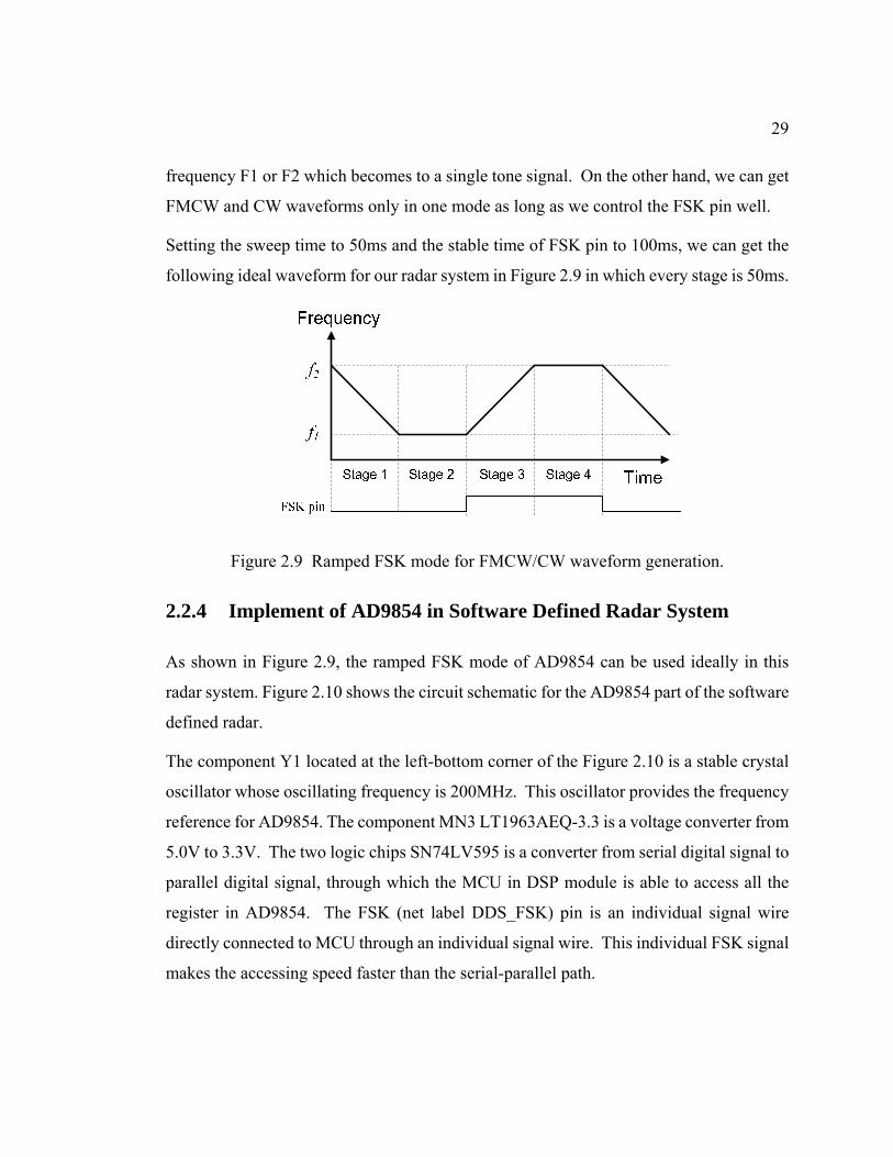
29
frequency F1 or F2 which becomes to a single tone signal. On the other hand, we can get
FMCW and CW waveforms only in one mode as long as we control the FSK pin well.
Setting the sweep time to 50ms and the stable time of FSK pin to 100ms, we can get the
following ideal waveform for our radar system in Figure 2.9 in which every stage is 50ms.
Figure 2.9 Ramped FSK mode for FMCW/CW waveform generation.
2.2.4 Implement of AD9854 in Software Defined Radar System
As shown in Figure 2.9, the ramped FSK mode of AD9854 can be used ideally in this
radar system. Figure 2.10 shows the circuit schematic for the AD9854 part of the software
defined radar.
The component Y1 located at the left-bottom corner of the Figure 2.10 is a stable crystal
oscillator whose oscillating frequency is 200MHz. This oscillator provides the frequency
reference for AD9854. The component MN3 LT1963AEQ-3.3 is a voltage converter from
5.0V to 3.3V. The two logic chips SN74LV595 is a converter from serial digital signal to
parallel digital signal, through which the MCU in DSP module is able to access all the
register in AD9854. The FSK (net label DDS_FSK) pin is an individual signal wire
directly connected to MCU through an individual signal wire. This individual FSK signal
makes the accessing speed faster than the serial-parallel path.
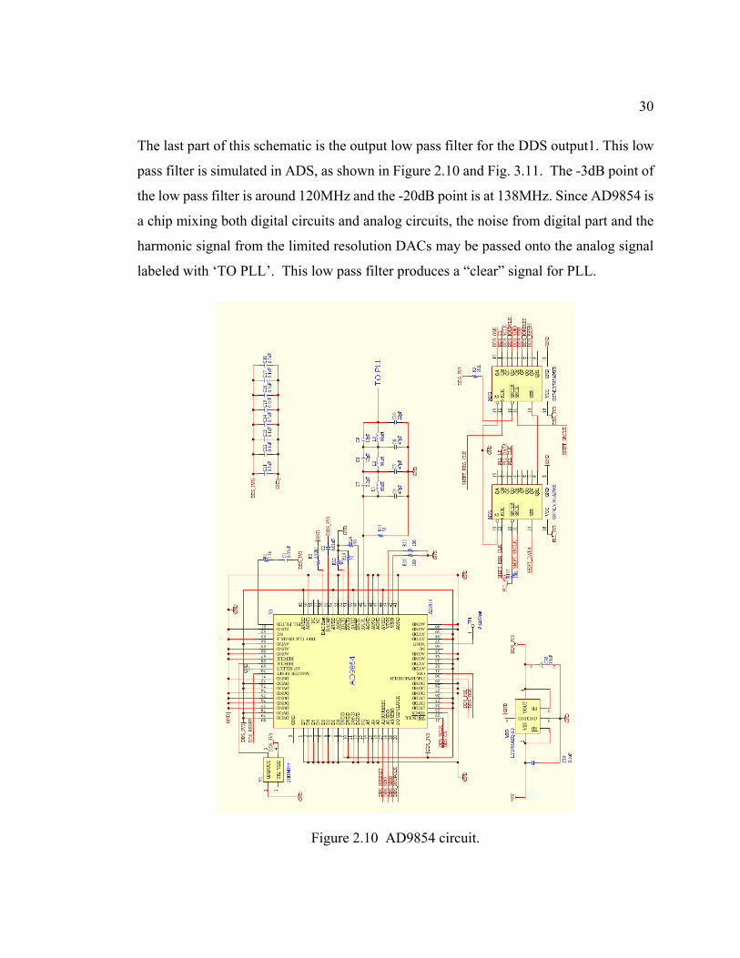
30
The last part of this schematic is the output low pass filter for the DDS output1. This low
pass filter is simulated in ADS, as shown in Figure 2.10 and Fig. 3.11. The -3dB point of
the low pass filter is around 120MHz and the -20dB point is at 138MHz. Since AD9854 is
a chip mixing both digital circuits and analog circuits, the noise from digital part and the
harmonic signal from the limited resolution DACs may be passed onto the analog signal
labeled with ‘TO PLL’. This low pass filter produces a “clear” signal for PLL.
Figure 2.10 AD9854 circuit.
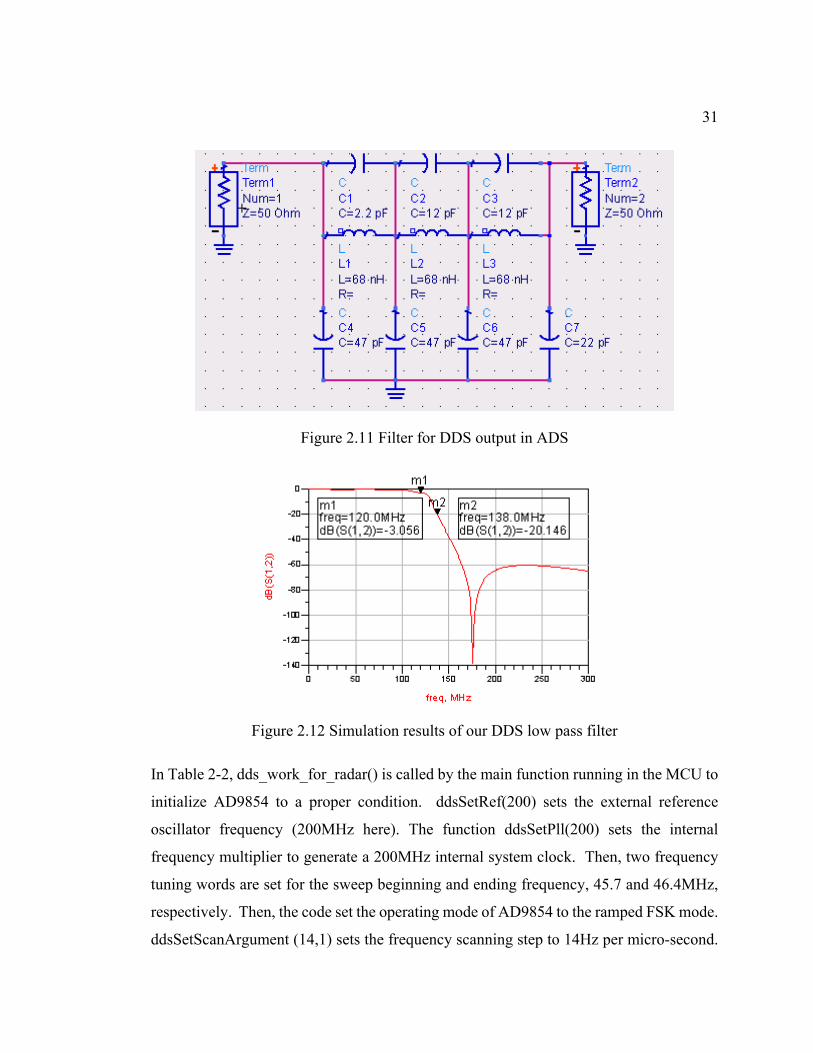
31
Figure 2.11 Filter for DDS output in ADS
Figure 2.12 Simulation results of our DDS low pass filter
In Table 2-2, dds_work_for_radar() is called by the main function running in the MCU to
initialize AD9854 to a proper condition. ddsSetRef(200) sets the external reference
oscillator frequency (200MHz here). The function ddsSetPll(200) sets the internal
frequency multiplier to generate a 200MHz internal system clock. Then, two frequency
tuning words are set for the sweep beginning and ending frequency, 45.7 and 46.4MHz,
respectively. Then, the code set the operating mode of AD9854 to the ramped FSK mode.
ddsSetScanArgument (14,1) sets the frequency scanning step to 14Hz per micro-second.
32
Lines 11 and 12 set the DAC output magnitude to maximum by writing 0xFFF to register
No.8. At last, DDSGo() validates all of the above settings and starts AD9854 in the
corresponding mode.
Table 2-2 Initialization code of AD9854
2.3. Phase Locked Loop (PLL)
The highest frequency of DDS is limited by the speed of digital logical circuits, DAC, and
power efficiency. Following the DDS, a phase-locked loop is implemented to generate the
transmitting microwave signal, as shown in Figure 2.1 Diagram of Frequency
Synthesizer.
A PLL is a circuit synchronizing an output (generated by VCO in most cases) signal’s
frequency and phase to its reference signal’s. In the synchronized (often called locked)
state the phase error between the oscillator’s output signal and the reference signal is zero
or a constant value. There are a number of types of PLL, e.g., linear PLL (LPLL), digital
PLLs (DPLL), all-digital PLLs (ADPLLs), and software PLLs (SPLL) [22]. Among the
1. #define DDS_LOW_FREQ_MHZ 45.7 2. #define DDS_HIGH_FREQ_MHZ 46.4 3. 4. void dds_work_for_radar(void) 5. { 6. ddsSetRefClk(200); //MHz 7. ddsSetPll(200); //MHz 8. ddsSetF1F2(45.7,46.4); //MHz 9. ddsSetOperationMode(DDS_MODE_RAMPED_FSK); 10. ddsSetScanArgument(14,1); 11. OutputShapedKeyingIMultiplier = 0xFFF; 12. OUTREG(8); 13. DDSGo(); 14. }
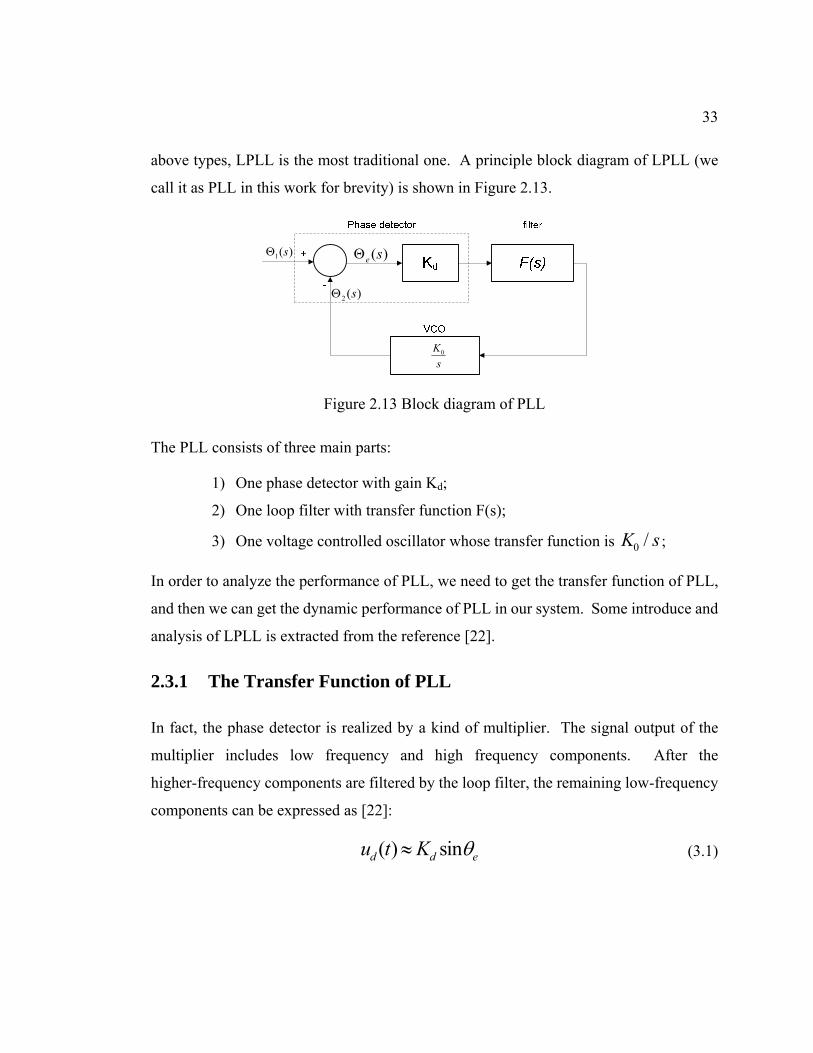
33
above types, LPLL is the most traditional one. A principle block diagram of LPLL (we
call it as PLL in this work for brevity) is shown in Figure 2.13.
2 ( )sΘ
1( )sΘ ( )e sΘ
0Ks
Figure 2.13 Block diagram of PLL
The PLL consists of three main parts:
1) One phase detector with gain Kd;
2) One loop filter with transfer function F(s);
3) One voltage controlled oscillator whose transfer function is 0 /K s ;
In order to analyze the performance of PLL, we need to get the transfer function of PLL,
and then we can get the dynamic performance of PLL in our system. Some introduce and
analysis of LPLL is extracted from the reference [22].
2.3.1 The Transfer Function of PLL
In fact, the phase detector is realized by a kind of multiplier. The signal output of the
multiplier includes low frequency and high frequency components. After the
higher-frequency components are filtered by the loop filter, the remaining low-frequency
components can be expressed as [22]:
( ) sind d eu t K θ≈ (3.1)
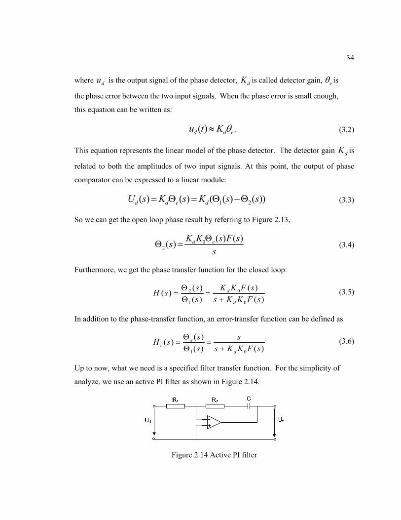
34
where du is the output signal of the phase detector, dK is called detector gain, eθ is
the phase error between the two input signals. When the phase error is small enough,
this equation can be written as:
( )d d eu t K θ≈ . (3.2)
This equation represents the linear model of the phase detector. The detector gain dK is
related to both the amplitudes of two input signals. At this point, the output of phase
comparator can be expressed to a linear module:
1 2( ) ( ) ( ( ) ( ))d d e dU s K s K s s= Θ = Θ −Θ (3.3)
So we can get the open loop phase result by referring to Figure 2.13,
02
( ) ( )( ) d eK K s F sss
ΘΘ = (3.4)
Furthermore, we get the phase transfer function for the closed loop:
2 0
1 0
( ) ( )( )( ) ( )
d
d
s K K F sH ss s K K F s
Θ= =Θ +
(3.5)
In addition to the phase-transfer function, an error-transfer function can be defined as
1 0
( )( )( ) ( )
ee
d
s sH ss s K K F s
Θ= =Θ +
(3.6)
Up to now, what we need is a specified filter transfer function. For the simplicity of
analyze, we use an active PI filter as shown in Figure 2.14.
Figure 2.14 Active PI filter
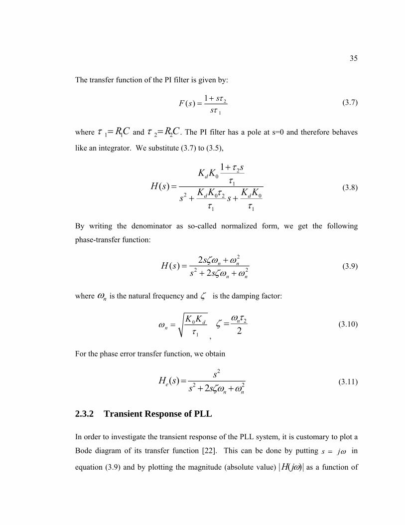
35
The transfer function of the PI filter is given by:
2
1
1( ) sF ssτ
τ+
= (3.7)
where 1 1RCτ = and 2 2R Cτ = . The PI filter has a pole at s=0 and therefore behaves
like an integrator. We substitute (3.7) to (3.5),
20
1
2 0 2 0
1 1
1
( )d
d d
sK KH s K K K Ks s
ττ
ττ τ
+
=+ +
(3.8)
By writing the denominator as so-called normalized form, we get the following
phase-transfer function:
2
2 2
2( )2
n n
n n
sH ss s
ζω ωζω ω+
=+ +
(3.9)
where nω is the natural frequency and ζ is the damping factor:
0
1
dn
K Kωτ
=, 2
2nωτζ = (3.10)
For the phase error transfer function, we obtain
2
2 2( )2e
n n
sH ss sζω ω
=+ +
(3.11)
2.3.2 Transient Response of PLL
In order to investigate the transient response of the PLL system, it is customary to plot a
Bode diagram of its transfer function [22]. This can be done by putting s jω= in
equation (3.9) and by plotting the magnitude (absolute value) | ( )|H jω as a function of
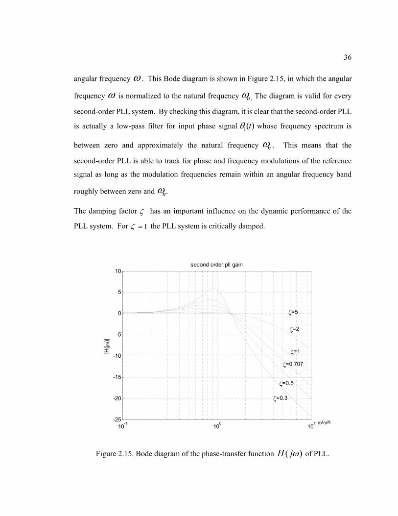
36
angular frequency ω . This Bode diagram is shown in Figure 2.15, in which the angular
frequency ω is normalized to the natural frequency nω . The diagram is valid for every
second-order PLL system. By checking this diagram, it is clear that the second-order PLL
is actually a low-pass filter for input phase signal 1( )tθ whose frequency spectrum is
between zero and approximately the natural frequency nω . This means that the second-order PLL is able to track for phase and frequency modulations of the reference
signal as long as the modulation frequencies remain within an angular frequency band
roughly between zero and nω .
The damping factor ζ has an important influence on the dynamic performance of the
PLL system. For 1ζ = the PLL system is critically damped.
Figure 2.15. Bode diagram of the phase-transfer function ( )H jω of PLL.
10-1 100 101-25
-20
-15
-10
-5
0
5
10
|H(j ω
)|
ω/ωn
second order pll gain
ζ=0.3
ζ=0.5
ζ=0.707
ζ=1
ζ=2
ζ=5
37
Figure 2.16. Simulation mode1 of PLL transient response with Simulink
Figure 2.17 Input of the 2nd order system
We use Simulink of Matlab to simulate the transient response of the 2nd order system and
the simulation model is shown in Figure 2.16. In Figure 2.16, 0.707ζ = and 1n=ω . In
this simulation, the input of system is a square wave. By adjusting the damping factor, we
can observe that the response changes. For the input shown in Figure 2.17, several
dynamic responses with 0.1~ 5ζ = are shown in Figure 2.18. Observing the simulation
results, the transient response becomes oscillatory, e.g. 0 .1ζ = if the damp factor is
made smaller than unity.
0 10 20 30 40 50 60 70 80 90 100-1
-0.5
0
0.5
1
Second
Am
plitu
de
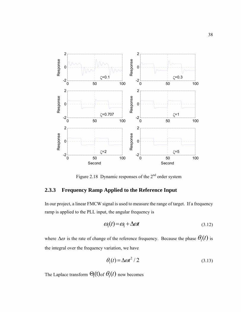
38
Figure 2.18 Dynamic responses of the 2nd order system
2.3.3 Frequency Ramp Applied to the Reference Input
In our project, a linear FMCW signal is used to measure the range of target. If a frequency
ramp is applied to the PLL input, the angular frequency is
1 1( )t tω ω ω= +Δ (3.12)
where ωΔ is the rate of change of the reference frequency. Because the phase 1( )tθ is
the integral over the frequency variation, we have
21( ) / 2t tθ ω=Δ (3.13)
The Laplace transform 1Θ(t)of 1( )tθ now becomes
0 50 100-2
0
2R
espo
nse
ζ=0.1
0 50 100-2
0
2
Res
pons
e
ζ=0.3
0 50 100-2
0
2
Res
pons
e
ζ=0.707
0 50 100-2
0
2
Res
pons
e
ζ=1
0 50 100-2
0
2
Second
Res
pons
e
ζ=2
0 50 100-2
0
2
Second
Res
pons
e
ζ=5
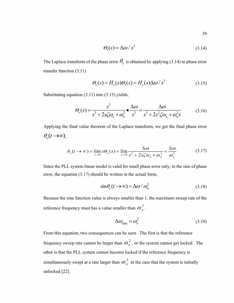
39
31( ) /Θ s sω=Δ (3.14)
The Laplace transform of the phase error eθ is obtained by applying (3.14) to phase error
transfer function (3.11)
31( ) ( ) ( ) ( ) /e e eΘ Θs H s s H s sω= = Δ (3.15)
Substituting equation (3.11) into (3.15) yields,
2
2 2 3 3 2 2( )2 2e
n n n n
Θss
s s s s s sω ω
ζω ω ζω ωΔ Δ
= • =+ + + +
(3.16)
Applying the final value theorem of the Laplace transform, we get the final phase error
( )e tθ →∞ ,
2 2 20 0( ) lim ( ) lim
2e es sn n n
Θt s ss s
θω ωζω ω ω→ →
Δ Δ→ ∞ = = =
+ + (3.17)
Since the PLL system linear model is valid for small phase error only, to the sine of phase
error, the equation (3.17) should be written in the actual form,
2sin ( ) /e ntθ ω ω→∞ =Δ (3.18)
Because the sine function value is always smaller than 1, the maximum sweep rate of the
reference frequency must has a value smaller than 2nω .
2max nω ωΔ = (3.19)
From this equation, two consequences can be seen. The first is that the reference
frequency sweep rate cannot be larger than 2nω , or the system cannot get locked. The
other is that the PLL system cannot become locked if the reference frequency is
simultaneously swept at a rate larger than 2nω in the case that the system is initially
unlocked [22].
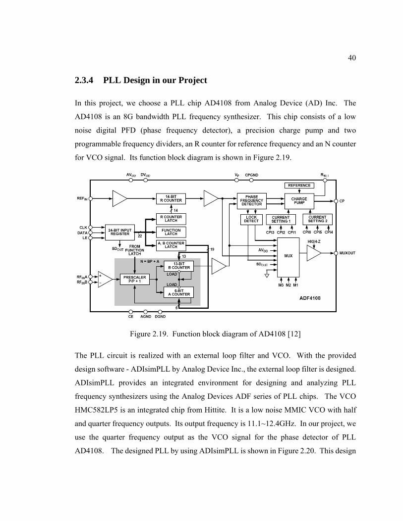
40
2.3.4 PLL Design in our Project
In this project, we choose a PLL chip AD4108 from Analog Device (AD) Inc. The
AD4108 is an 8G bandwidth PLL frequency synthesizer. This chip consists of a low
noise digital PFD (phase frequency detector), a precision charge pump and two
programmable frequency dividers, an R counter for reference frequency and an N counter
for VCO signal. Its function block diagram is shown in Figure 2.19.
Figure 2.19. Function block diagram of AD4108 [12]
The PLL circuit is realized with an external loop filter and VCO. With the provided
design software - ADIsimPLL by Analog Device Inc., the external loop filter is designed.
ADIsimPLL provides an integrated environment for designing and analyzing PLL
frequency synthesizers using the Analog Devices ADF series of PLL chips. The VCO
HMC582LP5 is an integrated chip from Hittite. It is a low noise MMIC VCO with half
and quarter frequency outputs. Its output frequency is 11.1~12.4GHz. In our project, we
use the quarter frequency output as the VCO signal for the phase detector of PLL
AD4108. The designed PLL by using ADIsimPLL is shown in Figure 2.20. This design
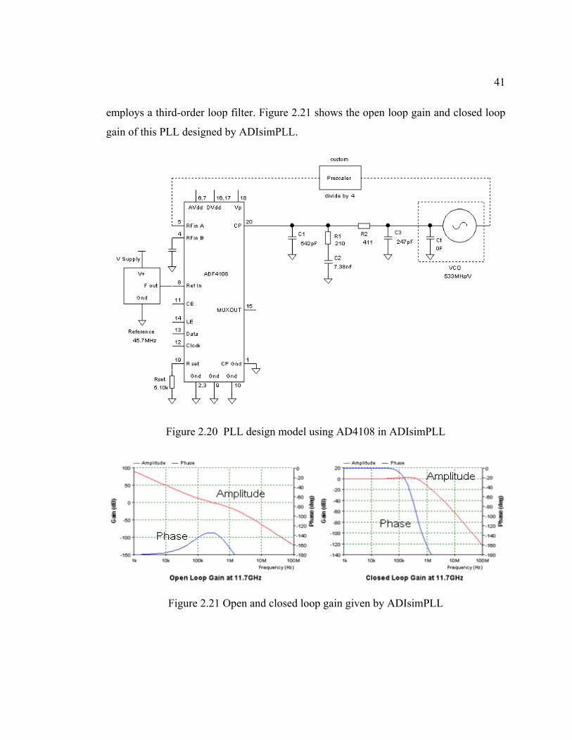
41
employs a third-order loop filter. Figure 2.21 shows the open loop gain and closed loop
gain of this PLL designed by ADIsimPLL.
Figure 2.20 PLL design model using AD4108 in ADIsimPLL
Figure 2.21 Open and closed loop gain given by ADIsimPLL
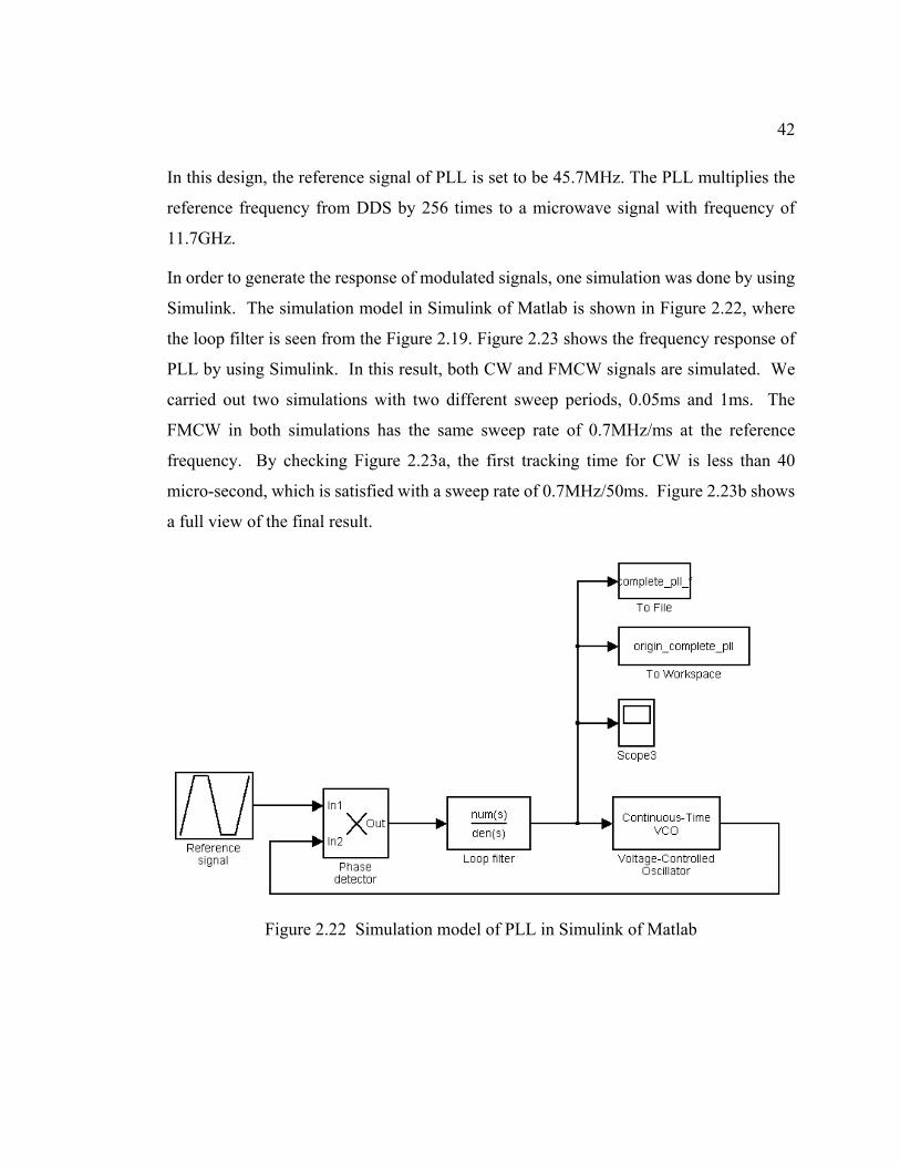
42
In this design, the reference signal of PLL is set to be 45.7MHz. The PLL multiplies the
reference frequency from DDS by 256 times to a microwave signal with frequency of
11.7GHz.
In order to generate the response of modulated signals, one simulation was done by using
Simulink. The simulation model in Simulink of Matlab is shown in Figure 2.22, where
the loop filter is seen from the Figure 2.19. Figure 2.23 shows the frequency response of
PLL by using Simulink. In this result, both CW and FMCW signals are simulated. We
carried out two simulations with two different sweep periods, 0.05ms and 1ms. The
FMCW in both simulations has the same sweep rate of 0.7MHz/ms at the reference
frequency. By checking Figure 2.23a, the first tracking time for CW is less than 40
micro-second, which is satisfied with a sweep rate of 0.7MHz/50ms. Figure 2.23b shows
a full view of the final result.
Figure 2.22 Simulation model of PLL in Simulink of Matlab
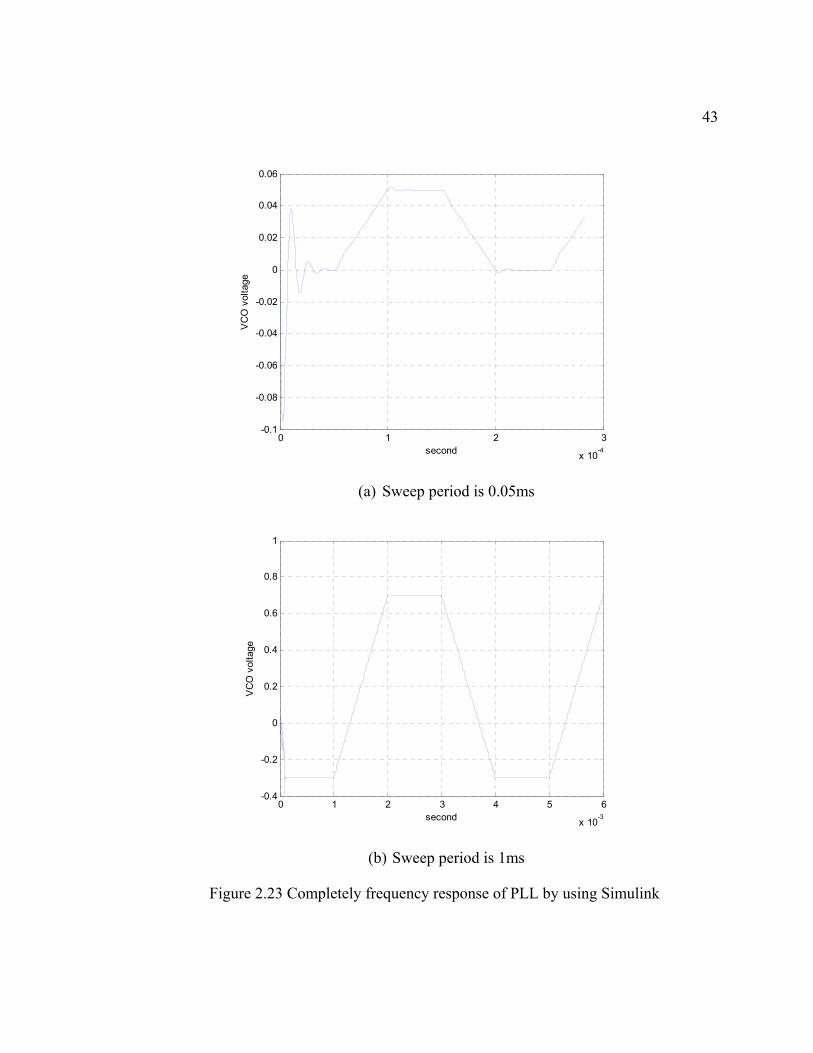
43
(a) Sweep period is 0.05ms
(b) Sweep period is 1ms
Figure 2.23 Completely frequency response of PLL by using Simulink
0 1 2 3
x 10-4
-0.1
-0.08
-0.06
-0.04
-0.02
0
0.02
0.04
0.06
second
VC
O v
olta
ge
0 1 2 3 4 5 6
x 10-3
-0.4
-0.2
0
0.2
0.4
0.6
0.8
1
second
VC
O v
olta
ge
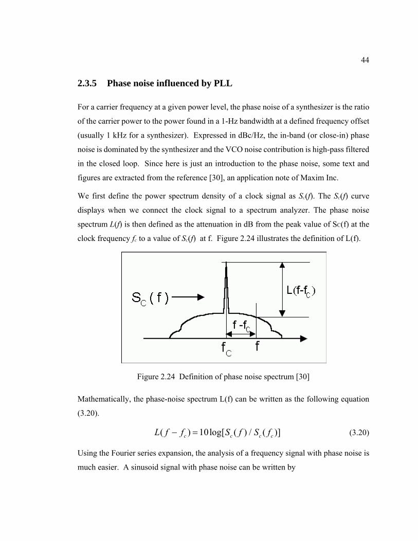
44
2.3.5 Phase noise influenced by PLL
For a carrier frequency at a given power level, the phase noise of a synthesizer is the ratio
of the carrier power to the power found in a 1-Hz bandwidth at a defined frequency offset
(usually 1 kHz for a synthesizer). Expressed in dBc/Hz, the in-band (or close-in) phase
noise is dominated by the synthesizer and the VCO noise contribution is high-pass filtered
in the closed loop. Since here is just an introduction to the phase noise, some text and
figures are extracted from the reference [30], an application note of Maxim Inc.
We first define the power spectrum density of a clock signal as SC(f). The SC(f) curve
displays when we connect the clock signal to a spectrum analyzer. The phase noise
spectrum L(f) is then defined as the attenuation in dB from the peak value of SC(f) at the
clock frequency fC to a value of SC(f) at f. Figure 2.24 illustrates the definition of L(f).
Figure 2.24 Definition of phase noise spectrum [30]
Mathematically, the phase-noise spectrum L(f) can be written as the following equation
(3.20).
( ) 10log[ ( ) / ( )]c c c cL f f S f S f− = (3.20)
Using the Fourier series expansion, the analysis of a frequency signal with phase noise is
much easier. A sinusoid signal with phase noise can be written by
45
( ) sin(2 ( ))cC t A f t tπ θ= + (3.21)
From equation (3.21), we see that the sinusoid signal is phase modulated by phase noise
( )tθ . As the phase noise is always much smaller than π/2, equation (3.21) can be
approximated by
( ) sin( ) ( )cos( )c cC t A t A t tω θ ω= + (3.22)
Using the Fourier series expansion, the spectrum of C(t) is then
2 2
( ) [ ( ) ( )] [ ( ) ( )]4 4C c c c cA AS f f f f f S f f S f fθ θδ δ= − + + + − + + (3.23)
where ( )S fθ is the spectrum of ( )tθ . Using the definition of L(f), we have
( ) 10log[ ( ) / ( )] 10log[ ( )]c c c c cL f f S f S f S f fθ− = = − (3.24)
This illustrates that L(f) is just ( )S fθ presented in dB. This also explains the real
meaning of L(f).
For a PLL frequency synthesis system, the final phase noise with the bandwidth is
20log( )final refL L N= + (3.25)
where refL is phase noise in dB of the reference clock, N is the frequency enlarge time.
In this system, N is 768, so the phase noise is increased by 20log(768)=57.7dB.
2.4. Experiment Result
A frequency tripler is used after the PLL to generate the required transmitting
millimeter-wave signal. For the convenience of our investigation, the complete frequency
synthesizer block diagram is shown again in Figure 2.25 and the frequency table is shown
again in Table 2-3.
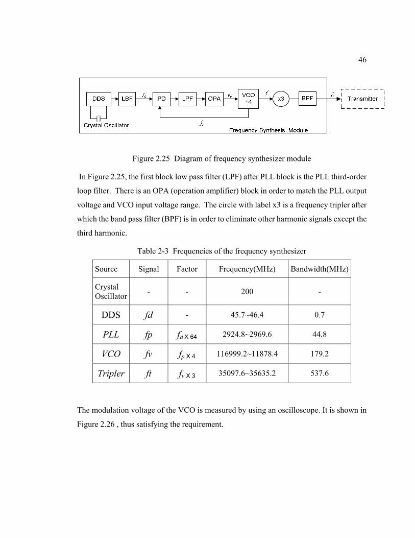
46
Figure 2.25 Diagram of frequency synthesizer module
In Figure 2.25, the first block low pass filter (LPF) after PLL block is the PLL third-order
loop filter. There is an OPA (operation amplifier) block in order to match the PLL output
voltage and VCO input voltage range. The circle with label x3 is a frequency tripler after
which the band pass filter (BPF) is in order to eliminate other harmonic signals except the
third harmonic.
Table 2-3 Frequencies of the frequency synthesizer
Source Signal Factor Frequency(MHz) Bandwidth(MHz)
Crystal Oscillator - - 200 -
DDS fd - 45.7~46.4 0.7
PLL fp fd Х 64 2924.8~2969.6 44.8
VCO fv fp Х 4 116999.2~11878.4 179.2
Tripler ft fv Х 3 35097.6~35635.2 537.6
The modulation voltage of the VCO is measured by using an oscilloscope. It is shown in
Figure 2.26 , thus satisfying the requirement.
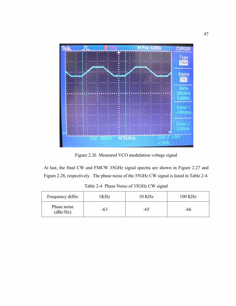
47
Figure 2.26 Measured VCO modulation voltage signal
At last, the final CW and FMCW 35GHz signal spectra are shown in Figure 2.27 and
Figure 2.28, respectively. The phase noise of the 35GHz CW signal is listed in Table 2-4.
Table 2-4 Phase Noise of 35GHz CW signal
Frequency differ 1KHz 10 KHz 100 KHz
Phase noise (dBc/Hz) -63 -65 -66
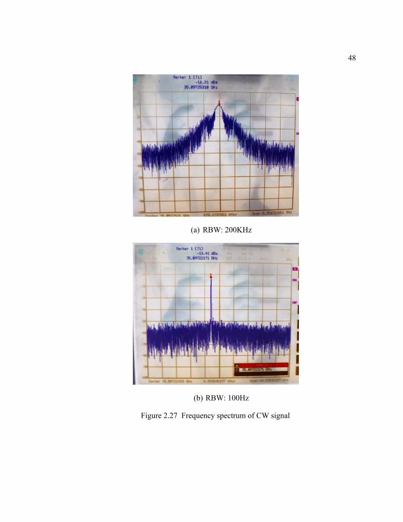
48
(a) RBW: 200KHz
(b) RBW: 100Hz
Figure 2.27 Frequency spectrum of CW signal
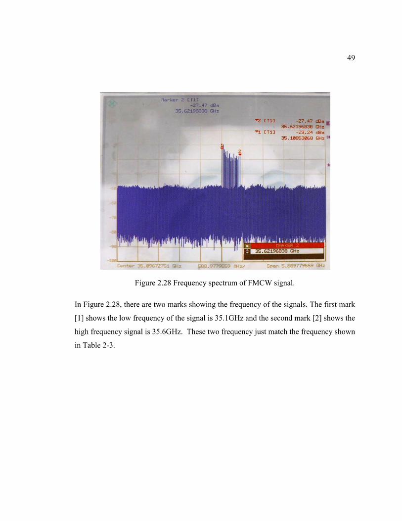
49
Figure 2.28 Frequency spectrum of FMCW signal.
In Figure 2.28, there are two marks showing the frequency of the signals. The first mark
[1] shows the low frequency of the signal is 35.1GHz and the second mark [2] shows the
high frequency signal is 35.6GHz. These two frequency just match the frequency shown
in Table 2-3.
50
CHAPTER 3 DIGITAL SIGNAL PROCESSING
The high frequency signal is radiated to free space by the transmitting antenna and
reflected back by targets in certain application scenarios. The reflected signal is then
acquired by the receiving antennas. Then, the received signal is demodulated by a receiver
and then amplified. The amplified analog signals are converted to digital signals by
ADCs and sent into DSP module. At last, the DSP unit executes the algorithms for
obtaining the target speed, range and angle of the targets.
3.1. Fast Fourier Transform
In the beginning, the hardware architecture is discussed and implemented. All the system
functions have to be processed by a software platform. Based on the discussion in
Chapter 2, the speed and range are contained in the frequency shift, namely the Doppler
frequency shift for the speed and FMCW frequency shift for the range. Moreover, for the
angle measurement, phase information is needed for the original data. The most
fundamental method to estimate frequency spectrum of a finite-length digital sequence is
the FFT. Based on the spectrum, the target data could be calculated and finally the
moving parameters of target can be obtained from the system operational parameters for
both CW and FMCW.
The FFT algorithm is well-known and it is the most commonly used algorithm to get the
frequency spectrum of a finite-length digital sequence signal. In the following, a brief
description of FFT started by the definition of discrete Fourier transform (DFT) will be
shown. Some of this part is extracted from reference [25] and [26].
The DFT of a finite-time sequence is defined as
1
0
( ) [ ]N
nkN
n
X k x n W−
=
=∑ (4.1)
where
51
X[k]: Frequency sampled data;
x[n]: Time sampled data;
N: Total number of samples;
n: Time index, n = 0,1,2,3…N-1;
k: Freq index, k = 0,1,2,3…N-1;
NW : A shorthand for the factor which is
(2 / )j NNW e π−= (4.2)
Obviously, simple iterative calculation based on equation (4.1) requires a very large
amount of computational efforts. The complex operation is on the order of O(N2), where
O(N2) means proportional to N2. The FFT is a very efficient way to compute the full
frequency sequence data for a series of sampled data in the time domain.
In order to decrease the computational time of a DFT, the famous FFT algorithm was
firstly proposed by J. W. Cooley and J. Tukey, and it is the most common FFT algorithm.
The basic concept of FFT is to break a large DFT of N= N1N2 into two smaller DFTs of
sizes N1 and N2. This operation is done recursively until it cannot be further broken down
any more. By doing so, the last DFT could be only 2 points DFT if N is the mth order of 2.
This kind of algorithm is called a radix-2 FFT since the basic calculation is a 2 point DFT.
The complexity of radix-2 FFT can drop down to O (Nlog2N).
After Cooley-Tukey, numerous algorithms and commercially available software
packages have been developed. Most of them are written in radix 2, 4, 8 or mixed radix
8(4x2). Generally speaking, the mixed radix algorithm is much faster but much more
complicated than the radix-2 FFT.
Here is a simplified introduction for the radix-2 FFT. From the definition of DFT
equation(4.1), if N = 2v, we can get
52
1
0( ) [ ]
Nnk
Nn
X k x n W−
=
=∑
even odd
[ ] [ ]nk nkN N
n nx n W x n W= +∑ ∑
/2 1 /2 1
2 (2 1)
0 0[2 ] [2 1]
N Nmk m k
N Nm m
x m W x m W− −
+
= =
= + +∑ ∑ (4.3)
Since WN2 = WN/2, equation(4.3) can be rewritten in the form of
/2 1 /2 1
1 /2 20 0
1 2
( ) [ ] [ ]
( ) ( ), N = 0,1,2.....N-1
N Nmk k mk
N N Nm m
kN
X k f m W W f m W
F k W F k
− −
= =
= +
= +
∑ ∑ (4.4)
where f1[m]=x[2m] and f2[m]=x[2m+1], F1(k) and F2(k) are the N/2-point DFTs of the
sequences f1(m) and f2(m), respectively. By recursively doing this on F1(k) and F2(k), at
last all that we get are 2 points DFTs, which is very simple to calculate. After each
breaking-down, the number of samples drops down to half of the original sample number.
Obviously, the number of computation stages is log2N in order to get all 2 DFTs.
For example N=8, the whole computation procedure can be perform in log28=3 stages,
beginning with the computations of four two-point DFTs, then two four-point DFTs, and
finally, one eight-point DFT. The combination for the smaller DFTs to form the larger
DFT is illustrated in Figure 3.1 for N = 8. The basic computation in this procedure is
shown in Figure 3.2, which shows the so-called butterfly computation.
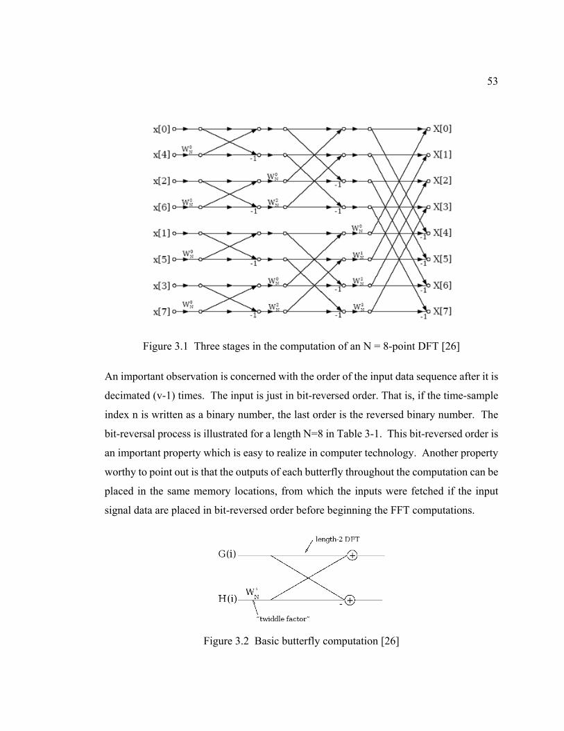
53
Figure 3.1 Three stages in the computation of an N = 8-point DFT [26]
An important observation is concerned with the order of the input data sequence after it is
decimated (v-1) times. The input is just in bit-reversed order. That is, if the time-sample
index n is written as a binary number, the last order is the reversed binary number. The
bit-reversal process is illustrated for a length N=8 in Table 3-1. This bit-reversed order is
an important property which is easy to realize in computer technology. Another property
worthy to point out is that the outputs of each butterfly throughout the computation can be
placed in the same memory locations, from which the inputs were fetched if the input
signal data are placed in bit-reversed order before beginning the FFT computations.
Figure 3.2 Basic butterfly computation [26]
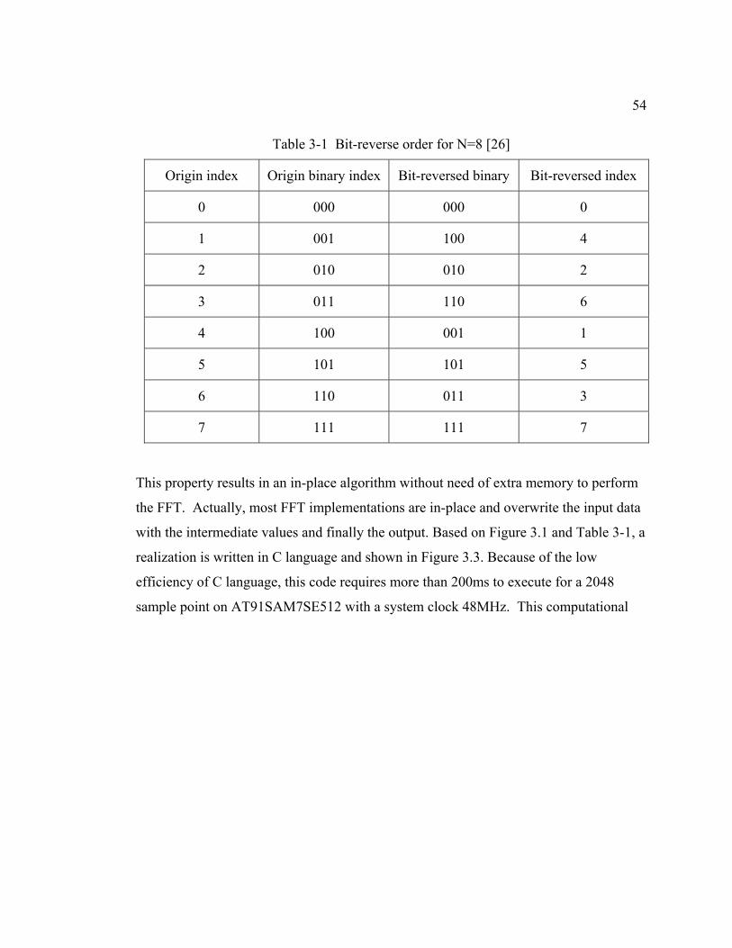
54
Table 3-1 Bit-reverse order for N=8 [26]
Origin index Origin binary index Bit-reversed binary Bit-reversed index
0 000 000 0
1 001 100 4
2 010 010 2
3 011 110 6
4 100 001 1
5 101 101 5
6 110 011 3
7 111 111 7
This property results in an in-place algorithm without need of extra memory to perform
the FFT. Actually, most FFT implementations are in-place and overwrite the input data
with the intermediate values and finally the output. Based on Figure 3.1 and Table 3-1, a
realization is written in C language and shown in Figure 3.3. Because of the low
efficiency of C language, this code requires more than 200ms to execute for a 2048
sample point on AT91SAM7SE512 with a system clock 48MHz. This computational
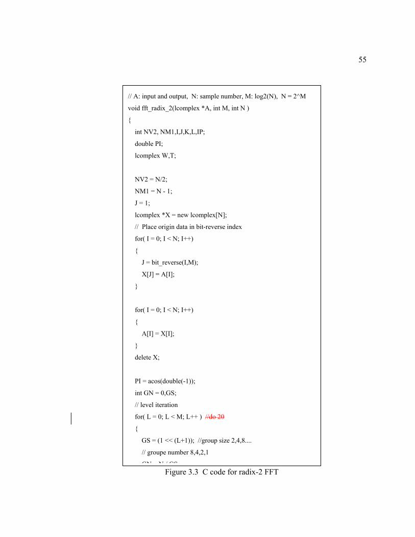
55
Figure 3.3 C code for radix-2 FFT
// A: input and output, N: sample number, M: log2(N), N = 2^M
void fft_radix_2(lcomplex *A, int M, int N )
{
int NV2, NM1,I,J,K,L,IP;
double PI;
lcomplex W,T;
NV2 = N/2;
NM1 = N - 1;
J = 1;
lcomplex *X = new lcomplex[N];
// Place origin data in bit-reverse index
for( I = 0; I < N; I++)
{
J = bit_reverse(I,M);
X[J] = A[I];
}
for( I = 0; I < N; I++)
{
A[I] = X[I];
}
delete X;
PI = acos(double(-1));
int GN = 0,GS;
// level iteration
for( L = 0; L < M; L++ ) //do 20
{
GS = (1 << (L+1)); //group size 2,4,8....
// groupe number 8,4,2,1
GN N / GS;
56
speed cannot be accepted by our real-time radar system. In order to yield a fast speed, this
code is re-written and the following changes are made:
1. Re-write in the assemble language;
2. Maximize the use of the registers in the RAM core;
3. Code and the constant values are copied to the internal SRAM after the startup of
the system;
4. W factor and bit-reverse array computation are firstly prepared at the startup of the
system;
After the optimization, the final execution time decreases to about 19ms for 2048 sample
points that is acceptable for this project.
3.2. General Concept of DSP System
Generally speaking, two basic elements are necessary in a DSP system, namely ADCs and
DSP core. The ADCs are needed to realize the conversion from analog signals to digital
signals. The performance of DSP core has to be good enough to execute the computing
task including all the algorithms and the control tasks at the same time. Despite of the
above two basic elements, there are also other auxiliary factors to be considered, such as
data and program storage, communication between device, computer, etc.
A basic function block diagram for a general DSP module is shown in Figure 3.4. In the
digital signal processing system, all the elements surrounding the DSP CORE are
connected to a system bus and a system clock. The system clock is also controlled by the
DSP CORE.
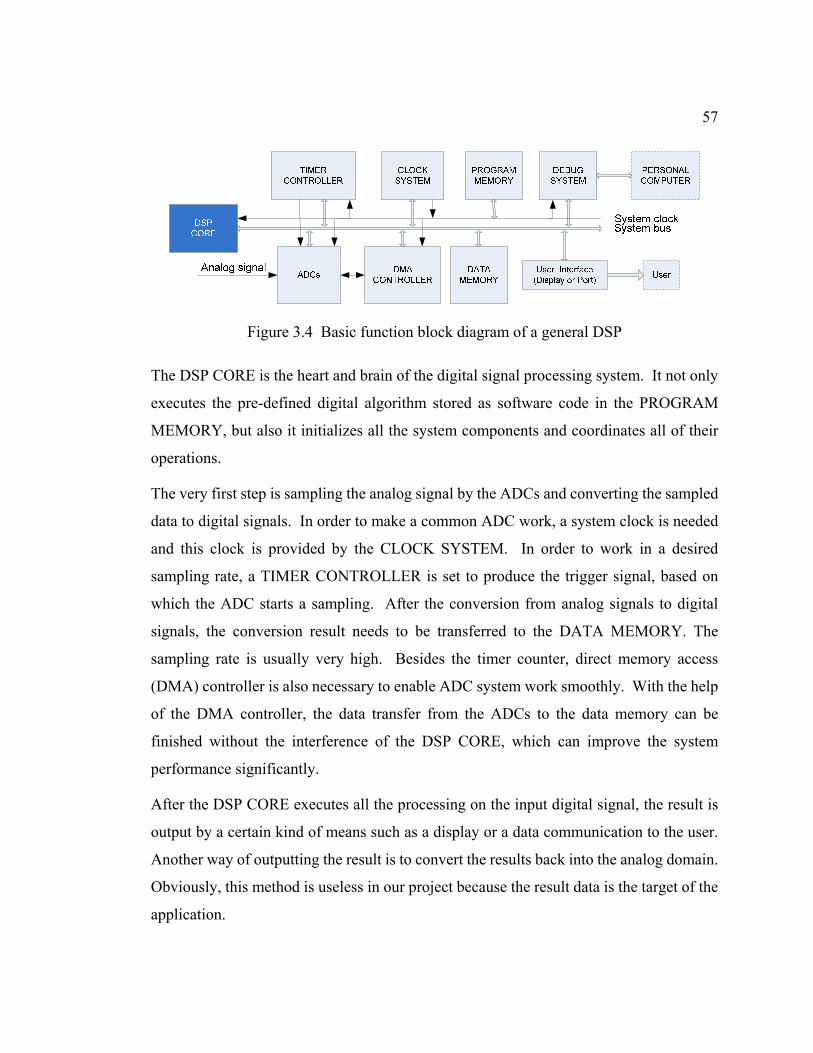
57
Figure 3.4 Basic function block diagram of a general DSP
The DSP CORE is the heart and brain of the digital signal processing system. It not only
executes the pre-defined digital algorithm stored as software code in the PROGRAM
MEMORY, but also it initializes all the system components and coordinates all of their
operations.
The very first step is sampling the analog signal by the ADCs and converting the sampled
data to digital signals. In order to make a common ADC work, a system clock is needed
and this clock is provided by the CLOCK SYSTEM. In order to work in a desired
sampling rate, a TIMER CONTROLLER is set to produce the trigger signal, based on
which the ADC starts a sampling. After the conversion from analog signals to digital
signals, the conversion result needs to be transferred to the DATA MEMORY. The
sampling rate is usually very high. Besides the timer counter, direct memory access
(DMA) controller is also necessary to enable ADC system work smoothly. With the help
of the DMA controller, the data transfer from the ADCs to the data memory can be
finished without the interference of the DSP CORE, which can improve the system
performance significantly.
After the DSP CORE executes all the processing on the input digital signal, the result is
output by a certain kind of means such as a display or a data communication to the user.
Another way of outputting the result is to convert the results back into the analog domain.
Obviously, this method is useless in our project because the result data is the target of the
application.
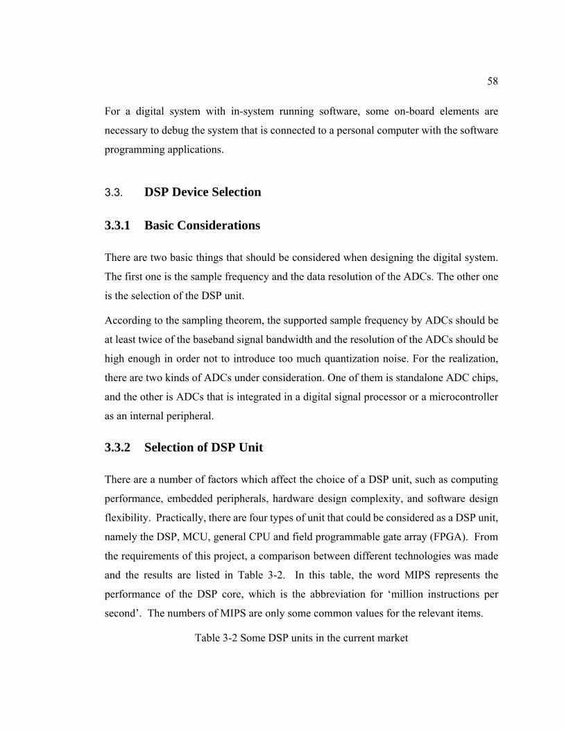
58
For a digital system with in-system running software, some on-board elements are
necessary to debug the system that is connected to a personal computer with the software
programming applications.
3.3. DSP Device Selection
3.3.1 Basic Considerations
There are two basic things that should be considered when designing the digital system.
The first one is the sample frequency and the data resolution of the ADCs. The other one
is the selection of the DSP unit.
According to the sampling theorem, the supported sample frequency by ADCs should be
at least twice of the baseband signal bandwidth and the resolution of the ADCs should be
high enough in order not to introduce too much quantization noise. For the realization,
there are two kinds of ADCs under consideration. One of them is standalone ADC chips,
and the other is ADCs that is integrated in a digital signal processor or a microcontroller
as an internal peripheral.
3.3.2 Selection of DSP Unit
There are a number of factors which affect the choice of a DSP unit, such as computing
performance, embedded peripherals, hardware design complexity, and software design
flexibility. Practically, there are four types of unit that could be considered as a DSP unit,
namely the DSP, MCU, general CPU and field programmable gate array (FPGA). From
the requirements of this project, a comparison between different technologies was made
and the results are listed in Table 3-2. In this table, the word MIPS represents the
performance of the DSP core, which is the abbreviation for ‘million instructions per
second’. The numbers of MIPS are only some common values for the relevant items.
Table 3-2 Some DSP units in the current market
59
Type Dedicated DSP MCU series General
CPU FPGA
Module Example TMS320Cxxx
ADSP-21xx MCS51 ARM7/9 x86
CYCLONE
VIRTEX
Bits width 32 8 32 32,64 Flexible
MIPS 100~2000+ 1~10 50~1000 2000+ PARALLEL
Communication ports Less Less A dozen No Flexible
Integrated ADCs No Some Some No No
Hardware Design
Complexity Difficult Very
easy Easy Very difficult Moderate
Software Design Complexity Difficult Very
easy Easy Moderate Very difficult
Computing performance of the DSP chip is the first factor to decide whether a chip is
suitable. Whether the device has integral ADCs and universal serial bus (USB) interface
is another important factor to be considered. In addition, a careful and complete
investigation is done on two categories; they are TMS320C6713 from TI and
AT91SAM7SE512 from Atmel, respectively.
Finally, it is concluded that the advanced RISC machine (ARM) technology is more
suitable as the DSP unit in our software-defined radar system. The following is a brief
introduction for the ARM technology. ARM is the name of a kind of MCU cores with
high performance and it is also the name of a company, which develops the ARM core
and gives the authorization to many partners for producing their own ARM products. All
the authorized companies are permitted to add any peripheral as many as they want. As
for ARM core itself, there are a number of versions, e.g. ARM7, ARM9, ARM11 and so
on. Among all the mentioned versions, ARM7 is the most popular one. ARM is basically
a kind of reduced instruction set computer (RISC) CPU. The most remarkable
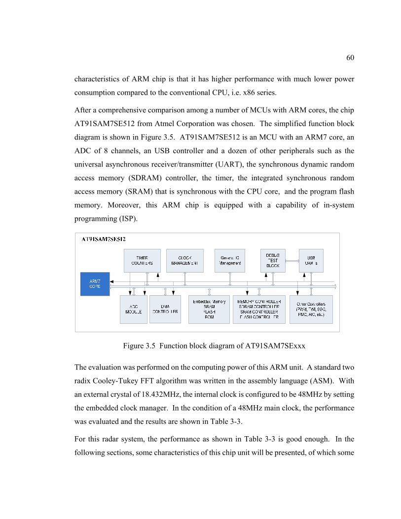
60
characteristics of ARM chip is that it has higher performance with much lower power
consumption compared to the conventional CPU, i.e. x86 series.
After a comprehensive comparison among a number of MCUs with ARM cores, the chip
AT91SAM7SE512 from Atmel Corporation was chosen. The simplified function block
diagram is shown in Figure 3.5. AT91SAM7SE512 is an MCU with an ARM7 core, an
ADC of 8 channels, an USB controller and a dozen of other peripherals such as the
universal asynchronous receiver/transmitter (UART), the synchronous dynamic random
access memory (SDRAM) controller, the timer, the integrated synchronous random
access memory (SRAM) that is synchronous with the CPU core, and the program flash
memory. Moreover, this ARM chip is equipped with a capability of in-system
programming (ISP).
Figure 3.5 Function block diagram of AT91SAM7SExxx
The evaluation was performed on the computing power of this ARM unit. A standard two
radix Cooley-Tukey FFT algorithm was written in the assembly language (ASM). With
an external crystal of 18.432MHz, the internal clock is configured to be 48MHz by setting
the embedded clock manager. In the condition of a 48MHz main clock, the performance
was evaluated and the results are shown in Table 3-3.
For this radar system, the performance as shown in Table 3-3 is good enough. In the
following sections, some characteristics of this chip unit will be presented, of which some
61
information is taken from reference [13], the datasheet of AT91SAM7SE512, Atmel
Corporation.
Table 3-3 Performance evaluation results
Code in Data in FFT point Time
SRAM SRAM 2048 19ms
1024 8ms
3.4. Peripheral in AT91SAM7SE512
3.4.1 The Analog Digital Convertor
There are eight ADC channels in this chip; nevertheless there is only one analog to digital
(AD) converter. Actually, an eight to one multiplexer is integrated in the chip with the
AD converter, which makes it possible to be connected to each of the eight analog
channels. The ADC is realized as a Successive Approximation Register (SAR) 10-bit
Analog-to-Digital Converter. As shown in Figure 3.6, the ADC converter is connected
with a multiplexer, timer counter channels, a peripheral DMA controller (PDC), and
advanced interrupt controller (AIC).
First of all, the following table (Table 3-4) shows the performance of the ADC in this
chip, which is excerpted from the datasheet of AT91SAM7SE512, Atmel Corporation.
As mentioned before, a timer counter and PDC are necessary to guarantee the ADC to
work properly. The timing relationship between ADC, Timer, PDC and memory is
shown in Figure 3.7.
In order to make sure the ADC functions properly with a precise sample frequency, it is
necessary that a timer is connected to the ADC. Any one of the three timer counter
channels inside the chip could be selected and connected to the ADC controller. Once the
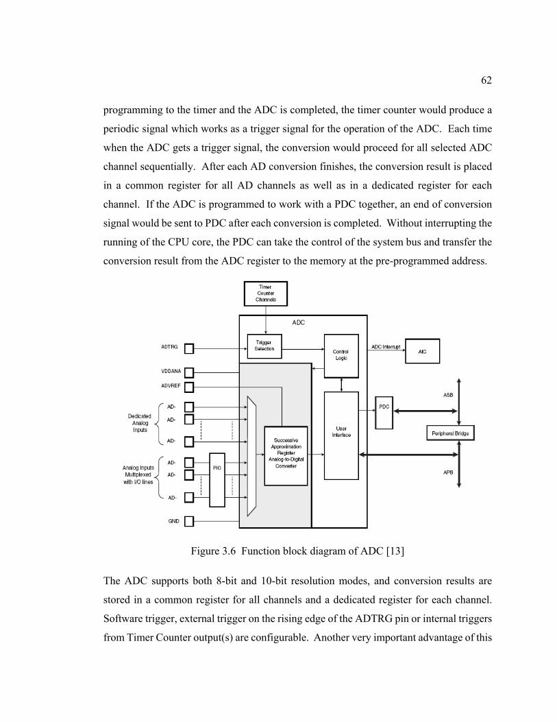
62
programming to the timer and the ADC is completed, the timer counter would produce a
periodic signal which works as a trigger signal for the operation of the ADC. Each time
when the ADC gets a trigger signal, the conversion would proceed for all selected ADC
channel sequentially. After each AD conversion finishes, the conversion result is placed
in a common register for all AD channels as well as in a dedicated register for each
channel. If the ADC is programmed to work with a PDC together, an end of conversion
signal would be sent to PDC after each conversion is completed. Without interrupting the
running of the CPU core, the PDC can take the control of the system bus and transfer the
conversion result from the ADC register to the memory at the pre-programmed address.
Figure 3.6 Function block diagram of ADC [13]
The ADC supports both 8-bit and 10-bit resolution modes, and conversion results are
stored in a common register for all channels and a dedicated register for each channel.
Software trigger, external trigger on the rising edge of the ADTRG pin or internal triggers
from Timer Counter output(s) are configurable. Another very important advantage of this
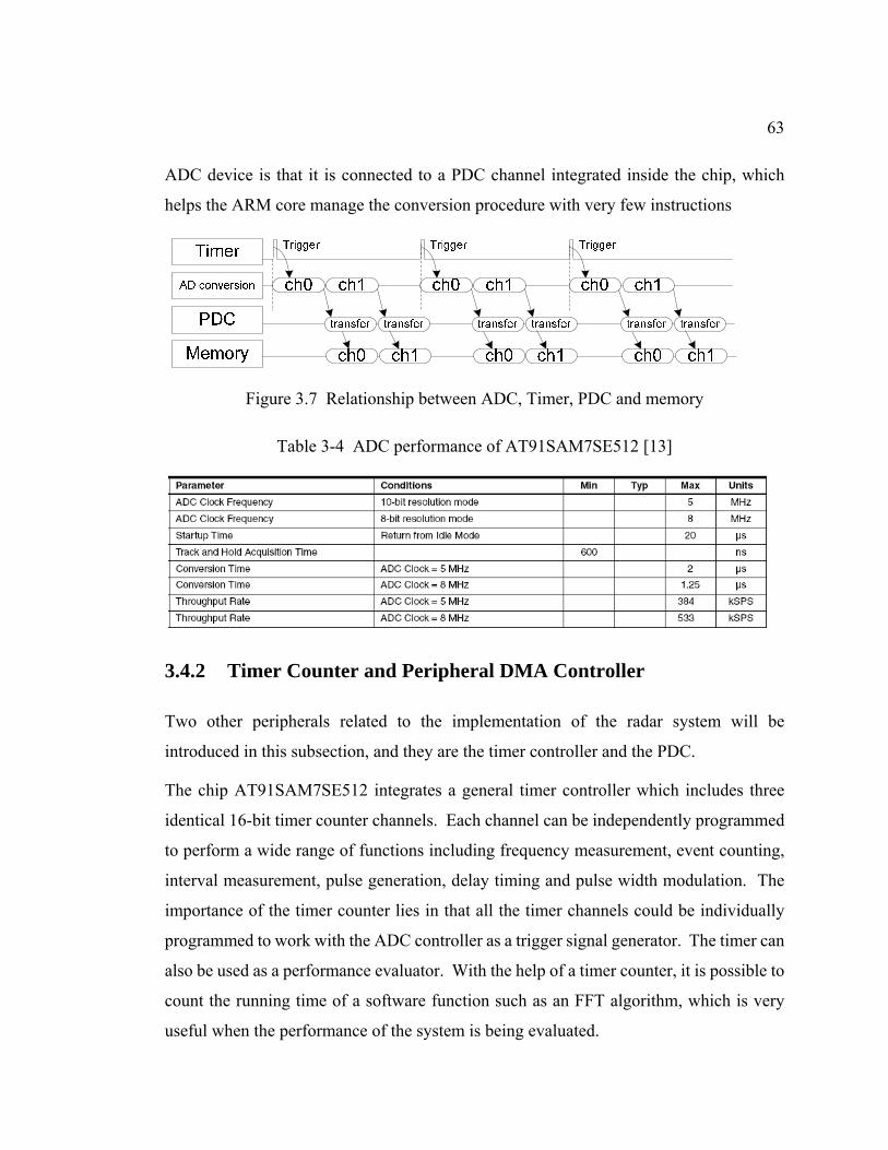
63
ADC device is that it is connected to a PDC channel integrated inside the chip, which
helps the ARM core manage the conversion procedure with very few instructions
Figure 3.7 Relationship between ADC, Timer, PDC and memory
Table 3-4 ADC performance of AT91SAM7SE512 [13]
3.4.2 Timer Counter and Peripheral DMA Controller
Two other peripherals related to the implementation of the radar system will be
introduced in this subsection, and they are the timer controller and the PDC.
The chip AT91SAM7SE512 integrates a general timer controller which includes three
identical 16-bit timer counter channels. Each channel can be independently programmed
to perform a wide range of functions including frequency measurement, event counting,
interval measurement, pulse generation, delay timing and pulse width modulation. The
importance of the timer counter lies in that all the timer channels could be individually
programmed to work with the ADC controller as a trigger signal generator. The timer can
also be used as a performance evaluator. With the help of a timer counter, it is possible to
count the running time of a software function such as an FFT algorithm, which is very
useful when the performance of the system is being evaluated.
64
Peripheral DMA controller is another important component integrated in the chip.
Generally, the integrated DMA controller transfers data between on-chip peripheral such
as the UART, the ADC and the on-chip/off-chip memory. Processor intervention can be
avoided and the processor interrupt-handling overhead can be removed if the peripheral
DMA controller is adopted. This significantly reduces the number of clock cycles
required for a data transfer and as a result, improves the performance of the
microcontroller and makes it more power efficient. For most peripherals, the DMA
channels are implemented in pairs, and each pair is dedicated to a particular peripheral.
One channel in the pair can be dedicated to the receiving channel and the other can be
dedicated to the transmitting channel. However, for the ADC controller, there is only one
channel instead of a pair since ADC doesn’t receive any data but only transmits data to the
ADC user.
3.4.3 USB and UART
The communication units of the AT91SAM7SE512 include a USB controller and three
UARTs. The USB Device Port (UDP) is compliant with the USB V2.0 full-speed device
specification. Since the USB has a feature of plug-and-play (PnP), we can use it as the
communication method between the computer and the radar device with great
convenience and high freedom. With the help of the full-speed at 12Mbit/s, we could
have fluent data communication between the radar and the computer for software
debugging, data analysis in the design stage but run as a regular device in the future. A
shortcoming for the USB should also be considered. The available communication
distance is very short which only is 5 meter [31].
Considering the practical application environment of the radar system, a much longer
distance between the radar device and the management system may be necessary. UART
is a kind of communication method based on which a longer valid communication
distance such as 15 meters or longer is possible when it works with a RS232
(Recommended Standard 232 by IEEE) standard electrical characteristics [23]. If a
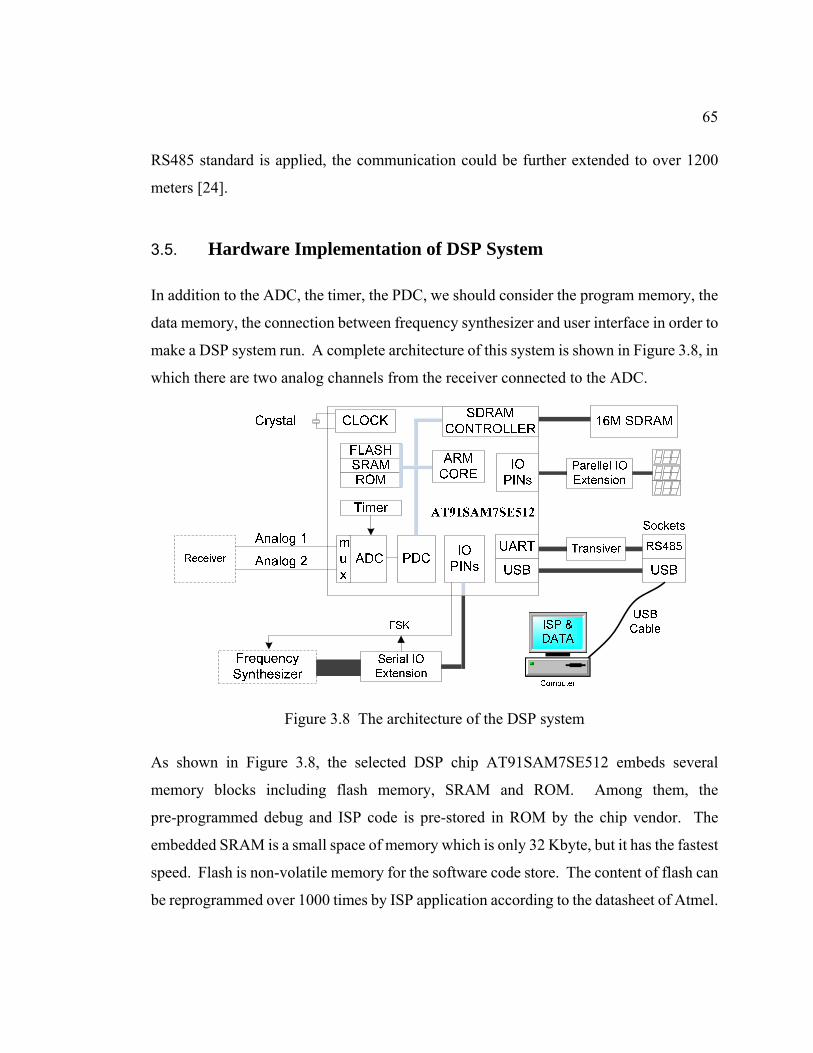
65
RS485 standard is applied, the communication could be further extended to over 1200
meters [24].
3.5. Hardware Implementation of DSP System
In addition to the ADC, the timer, the PDC, we should consider the program memory, the
data memory, the connection between frequency synthesizer and user interface in order to
make a DSP system run. A complete architecture of this system is shown in Figure 3.8, in
which there are two analog channels from the receiver connected to the ADC.
Figure 3.8 The architecture of the DSP system
As shown in Figure 3.8, the selected DSP chip AT91SAM7SE512 embeds several
memory blocks including flash memory, SRAM and ROM. Among them, the
pre-programmed debug and ISP code is pre-stored in ROM by the chip vendor. The
embedded SRAM is a small space of memory which is only 32 Kbyte, but it has the fastest
speed. Flash is non-volatile memory for the software code store. The content of flash can
be reprogrammed over 1000 times by ISP application according to the datasheet of Atmel.
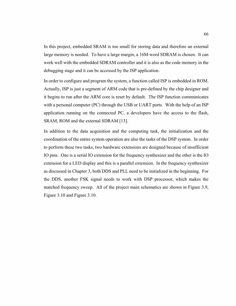
66
In this project, embedded SRAM is too small for storing data and therefore an external
large memory is needed. To have a large margin, a 16M-word SDRAM is chosen. It can
work well with the embedded SDRAM controller and it is also as the code memory in the
debugging stage and it can be accessed by the ISP application.
In order to configure and program the system, a function called ISP is embedded in ROM.
Actually, ISP is just a segment of ARM code that is pre-defined by the chip designer and
it begins to run after the ARM core is reset by default. The ISP function communicates
with a personal computer (PC) through the USB or UART ports. With the help of an ISP
application running on the connected PC, a developers have the access to the flash,
SRAM, ROM and the external SDRAM [13].
In addition to the data acquisition and the computing task, the initialization and the
coordination of the entire system operation are also the tasks of the DSP system. In order
to perform these two tasks, two hardware extensions are designed because of insufficient
IO pins. One is a serial IO extension for the frequency synthesizer and the other is the IO
extension for a LED display and this is a parallel extension. In the frequency synthesizer
as discussed in Chapter 3, both DDS and PLL need to be initialized in the beginning. For
the DDS, another FSK signal needs to work with DSP processor, which makes the
matched frequency sweep. All of the project main schematics are shown in Figure 3.9,
Figure 3.10 and Figure 3.10.
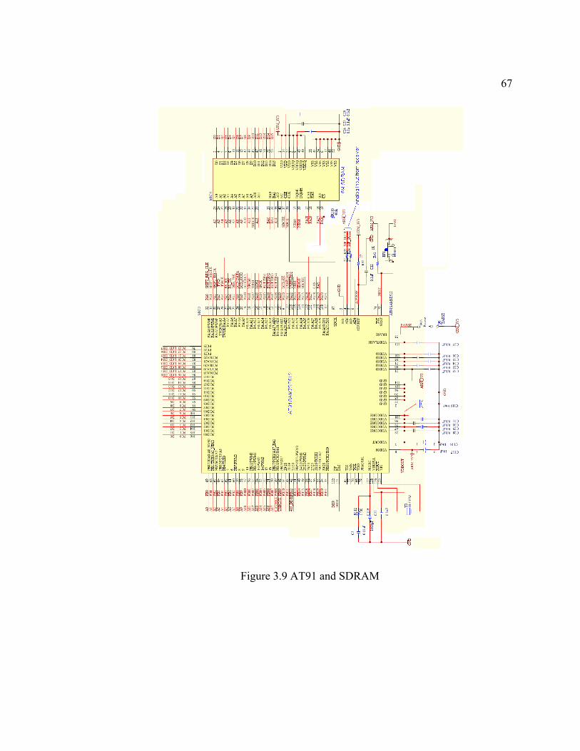
67
Figure 3.9 AT91 and SDRAM
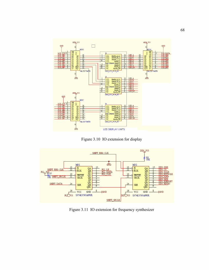
68
Figure 3.10 IO extension for display
Figure 3.11 IO extension for frequency synthesizer
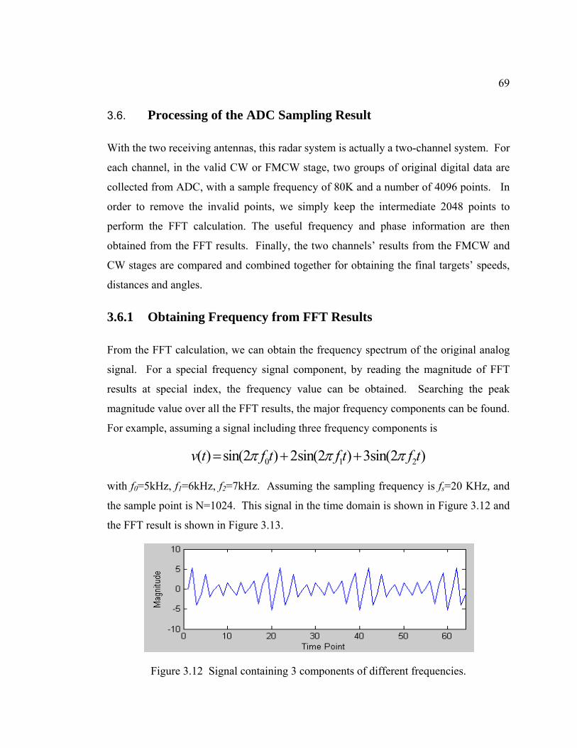
69
3.6. Processing of the ADC Sampling Result
With the two receiving antennas, this radar system is actually a two-channel system. For
each channel, in the valid CW or FMCW stage, two groups of original digital data are
collected from ADC, with a sample frequency of 80K and a number of 4096 points. In
order to remove the invalid points, we simply keep the intermediate 2048 points to
perform the FFT calculation. The useful frequency and phase information are then
obtained from the FFT results. Finally, the two channels’ results from the FMCW and
CW stages are compared and combined together for obtaining the final targets’ speeds,
distances and angles.
3.6.1 Obtaining Frequency from FFT Results
From the FFT calculation, we can obtain the frequency spectrum of the original analog
signal. For a special frequency signal component, by reading the magnitude of FFT
results at special index, the frequency value can be obtained. Searching the peak
magnitude value over all the FFT results, the major frequency components can be found.
For example, assuming a signal including three frequency components is
0 1 2( ) sin(2 ) 2sin(2 ) 3sin(2 )v t f t f t f tπ π π= + +
with f0=5kHz, f1=6kHz, f2=7kHz. Assuming the sampling frequency is fs=20 KHz, and
the sample point is N=1024. This signal in the time domain is shown in Figure 3.12 and
the FFT result is shown in Figure 3.13.
Figure 3.12 Signal containing 3 components of different frequencies.
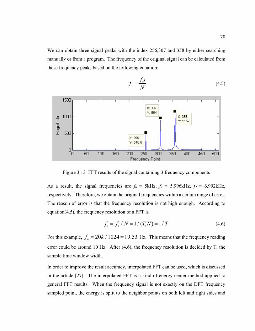
70
We can obtain three signal peaks with the index 256,307 and 358 by either searching
manually or from a program. The frequency of the original signal can be calculated from
these frequency peaks based on the following equation:
sf ifN
= (4.5)
Figure 3.13 FFT results of the signal containing 3 frequency components
As a result, the signal frequencies are f0 = 5kHz, f1 = 5.996kHz, f2 = 6.992kHz,
respectively. Therefore, we obtain the original frequencies within a certain range of error.
The reason of error is that the frequency resolution is not high enough. According to
equation(4.5), the frequency resolution of a FFT is
/ 1 / ( ) 1 /u s sf f N T N T= = = (4.6)
For this example, 20 / 1024 19.53uf k= = Hz. This means that the frequency reading
error could be around 10 Hz. After (4.6), the frequency resolution is decided by T, the
sample time window width.
In order to improve the result accuracy, interpolated FFT can be used, which is discussed
in the article [27]. The interpolated FFT is a kind of energy center method applied to
general FFT results. When the frequency signal is not exactly on the DFT frequency
sampled point, the energy is split to the neighbor points on both left and right sides and
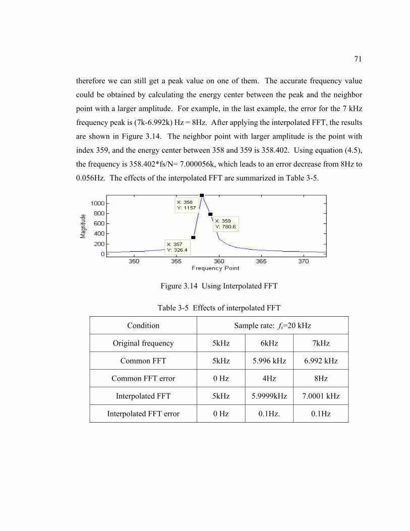
71
therefore we can still get a peak value on one of them. The accurate frequency value
could be obtained by calculating the energy center between the peak and the neighbor
point with a larger amplitude. For example, in the last example, the error for the 7 kHz
frequency peak is (7k-6.992k) Hz = 8Hz. After applying the interpolated FFT, the results
are shown in Figure 3.14. The neighbor point with larger amplitude is the point with
index 359, and the energy center between 358 and 359 is 358.402. Using equation (4.5),
the frequency is 358.402*fs/N= 7.000056k, which leads to an error decrease from 8Hz to
0.056Hz. The effects of the interpolated FFT are summarized in Table 3-5.
Figure 3.14 Using Interpolated FFT
Table 3-5 Effects of interpolated FFT
Condition Sample rate: fs=20 kHz
Original frequency 5kHz 6kHz 7kHz
Common FFT 5kHz 5.996 kHz 6.992 kHz
Common FFT error 0 Hz 4Hz 8Hz
Interpolated FFT 5kHz 5.9999kHz 7.0001 kHz
Interpolated FFT error 0 Hz 0.1Hz. 0.1Hz
72
3.6.2 Matching Frequency Results from the Two Channels
After we obtain the peak frequency points from the two FFT results, the data from two
channels must be combined and matched to each other. During the same stage including
one CW or FMCW sweep, since the reflected signal is from the same target at the same
time, the Doppler frequency or FMCW shift frequency for the two channels should have
the same value. In other words, two channels’ FFT results should have the same peak
frequency value. However, the extra and different peak frequencies occur in two channels
because the noise in each channel is different. The peak frequency from two channels has
to be processed to match with each other, and this job is easy for the C language.
3.6.3 Matching Results from FMCW and CW
If only one frequency is detected in both CW and FMCW stages, we can confirm that both
frequencies of CW and FMCW are from the same target, and the target’s movement
parameters can be calculated in case that the moving direction is known. The result is that
all sweep stages including more than one peak frequency are ignored and only the stages
including one peak frequency are kept. It was proved that this correction is valid and
essential in the on-road test.
In order to obtain the distance of a moving target by FMCW, there must be a known
Doppler frequency from the CW stage, as mentioned in above sections. After removing
the Doppler frequency from the FMCW frequency shift, the distance can be derived.
In the frequency decreasing FMCW stages, for an approaching target, the frequency
fmcwf should be
fmcw r d+ f f f= (4.7)
Then, simply the range frequency is
r fmcw d- f f f= (4.8)
73
For the receding target and in the frequency increasing FMCW stages, we have the same
results as (4.7) and (4.8).
Up to here, we get the range frequency rf and Doppler frequency df . It is easy to yield
the range, speed parameters in case that the direction of movement is known.
The last problem is to get the angle of the target. Since we have two receiving antennas,
we can have two signals with the same frequency but different phase. According to
section 2.4, let us assume that we have obtained the phase difference between two antenna
that is dϕ , then the angle of target is
0
arcsin2
dcdf
ϕθπ
⎛ ⎞= ⎜ ⎟
⎝ ⎠ , (4.9)
where c is the speed of light, d is the distance between the two receiving antennas, 0f is
the frequency of the radiated signal.
3.7. Software Structure and Flowchart
The software architecture is related to the system hardware structure, which includes the
frequency synthesizer, the user communication port, the display part, the debugging part
and so on. Corresponding to the components of hardware, the software is separated into
several file modules, which is shown in Figure 3.15.
In Figure 4.15, each file module is designed for the corresponding hardware operation.
Algorithm module is used to incorporate the algorithm as well as output the results.
OP595 is used to extend the serial to parallel IO for the initialization of both DDS and
PLL. SDRAM is also included as a software module because the SDRAM controller
should be initialized properly to work with the special SDRAM chip. CMD deal module
is designed for transferring original data and calculation results to PC, which receives and
executes the commands from a USB or UART port.
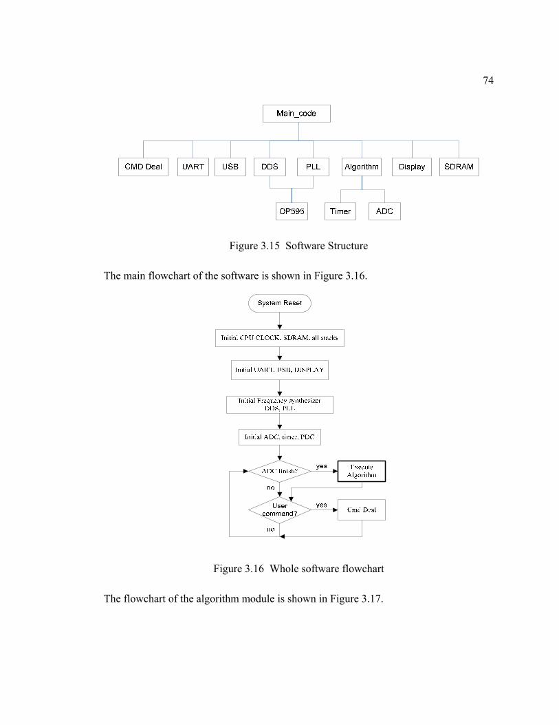
74
Figure 3.15 Software Structure
The main flowchart of the software is shown in Figure 3.16.
Figure 3.16 Whole software flowchart
The flowchart of the algorithm module is shown in Figure 3.17.
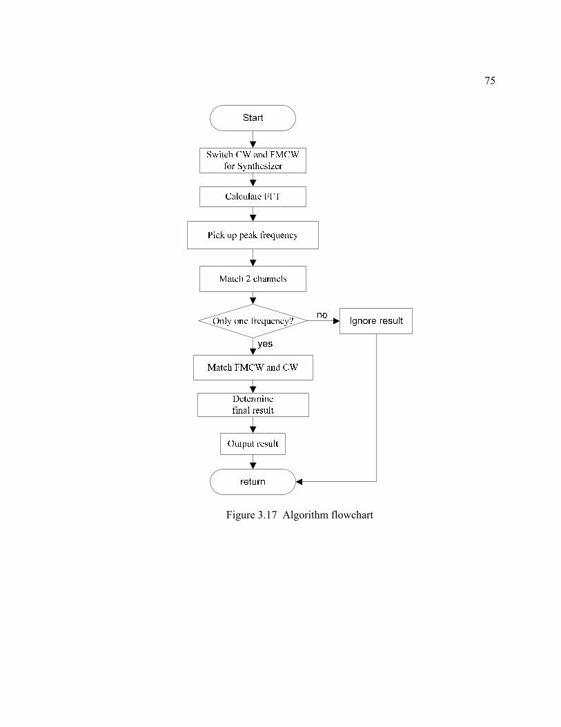
75
Figure 3.17 Algorithm flowchart
76
CHAPTER 4 SYSTEM IMPLEMENTATION AND
MEASUREMENTS
The hardware of the transceiver and antennas were finished by the project group. In
order to keep the completeness of this document, a brief description of transceiver and
antennas is presented in this chapter.
After the millimeter-wave signal is generated by the frequency synthesizer discussed in
Chapter 3, it is injected to the transmitter. Then it is transformed to electromagnetic wave
and radiated to free space by a directional antenna with high gain. In case that a target is
in the working range of the radar system, EMW would be reflected back by the target and
part of the EMW energy would be received by receiving antennas of the radar system.
The information of the target is contained in the carrier of received signal. The received
signal has a very high frequency carrier, 35.1GHz in our case, some kinds of frequency
down conversion or transformation should be realized by a receiver in order to obtain the
baseband signal for the digital signal processing system. In this project, the
transformation includes demodulating, filtering and amplifying.
4.1. Transmitter
The front end of the transceiver is combined in a single circuit board mounted on a metal
base. The whole function block diagram of the transceiver is shown in Figure 4.1.
As shown on the top center of Figure 4.1, the transmitter is following the frequency
synthesis module, which consists of a LNA and a PA whose gain are 22dB and 20dB,
respectively [14] [17]. In order to provide LO signal to the receiver, a power divider is
used to split the power of transmitting signal. The millimeter-wave signal is finally sent
to the transmitting antenna which has a gain of 20dBi. The final radiated power to space
is about 10mW.
In this radar system, the transmitting antenna and receiving antenna are separated into two
individual units to get a good isolation between transmitting and receiving. In order to
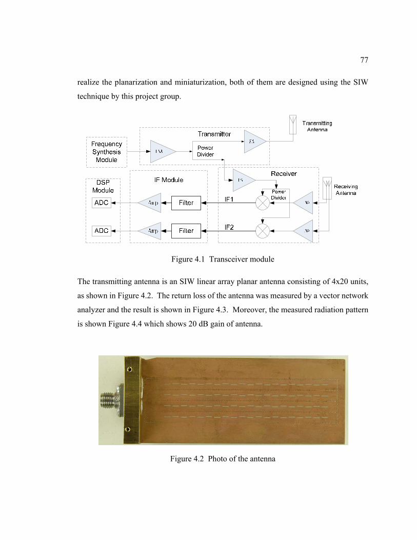
77
realize the planarization and miniaturization, both of them are designed using the SIW
technique by this project group.
Figure 4.1 Transceiver module
The transmitting antenna is an SIW linear array planar antenna consisting of 4x20 units,
as shown in Figure 4.2. The return loss of the antenna was measured by a vector network
analyzer and the result is shown in Figure 4.3. Moreover, the measured radiation pattern
is shown Figure 4.4 which shows 20 dB gain of antenna.
Figure 4.2 Photo of the antenna
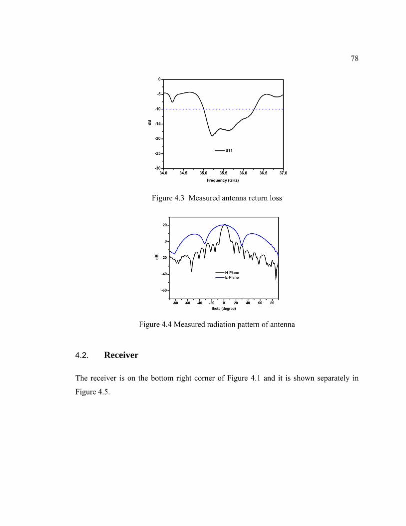
78
Figure 4.3 Measured antenna return loss
Figure 4.4 Measured radiation pattern of antenna
4.2. Receiver
The receiver is on the bottom right corner of Figure 4.1 and it is shown separately in
Figure 4.5.
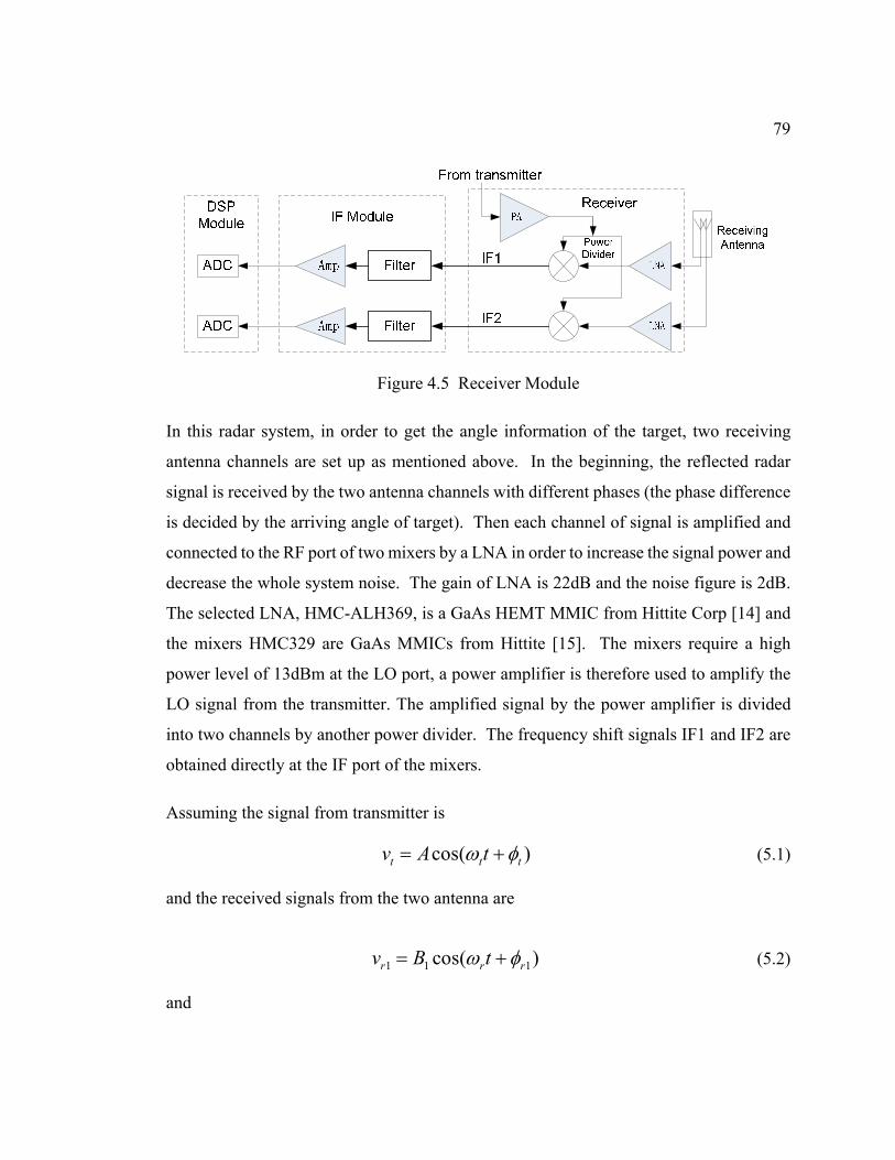
79
Figure 4.5 Receiver Module
In this radar system, in order to get the angle information of the target, two receiving
antenna channels are set up as mentioned above. In the beginning, the reflected radar
signal is received by the two antenna channels with different phases (the phase difference
is decided by the arriving angle of target). Then each channel of signal is amplified and
connected to the RF port of two mixers by a LNA in order to increase the signal power and
decrease the whole system noise. The gain of LNA is 22dB and the noise figure is 2dB.
The selected LNA, HMC-ALH369, is a GaAs HEMT MMIC from Hittite Corp [14] and
the mixers HMC329 are GaAs MMICs from Hittite [15]. The mixers require a high
power level of 13dBm at the LO port, a power amplifier is therefore used to amplify the
LO signal from the transmitter. The amplified signal by the power amplifier is divided
into two channels by another power divider. The frequency shift signals IF1 and IF2 are
obtained directly at the IF port of the mixers.
Assuming the signal from transmitter is
cos( )t t tv A tω φ= + (5.1)
and the received signals from the two antenna are
1 1 1cos( )r r rv B tω φ= + (5.2)
and
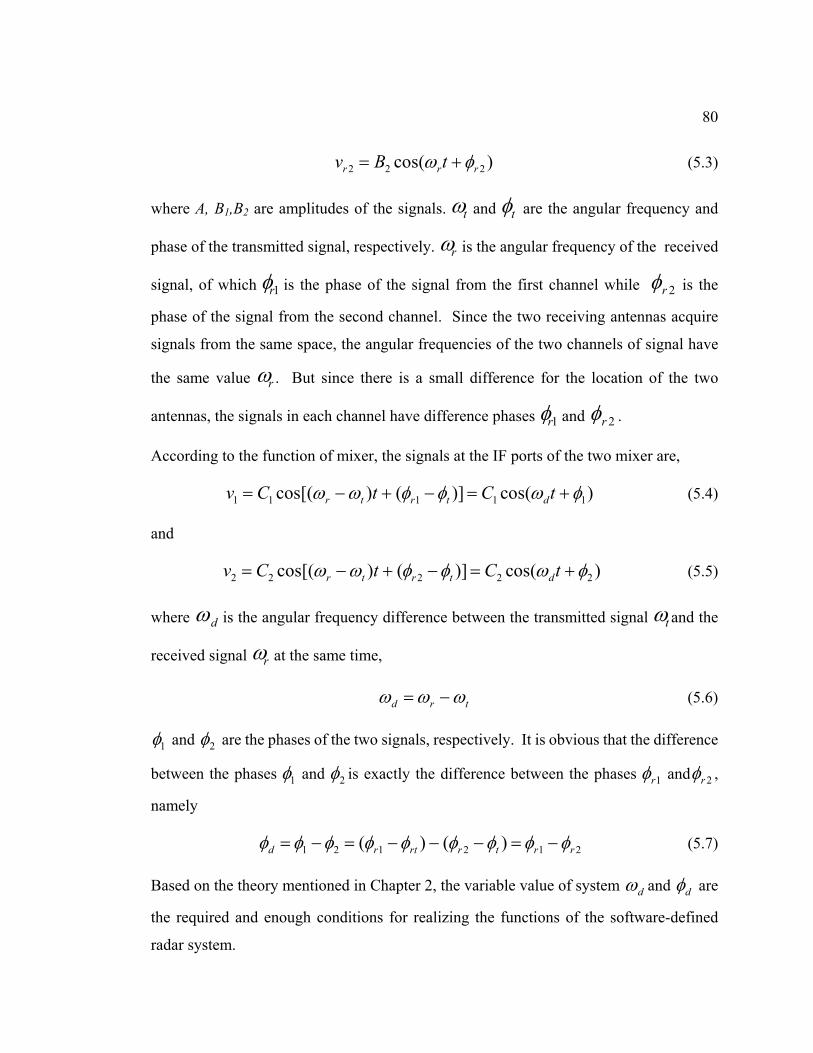
80
2 2 2cos( )r r rv B tω φ= + (5.3)
where A, B1,B2 are amplitudes of the signals. tω and tφ are the angular frequency and
phase of the transmitted signal, respectively. rω is the angular frequency of the received
signal, of which 1rφ is the phase of the signal from the first channel while 2rφ is the
phase of the signal from the second channel. Since the two receiving antennas acquire
signals from the same space, the angular frequencies of the two channels of signal have
the same value rω . But since there is a small difference for the location of the two
antennas, the signals in each channel have difference phases 1rφ and 2rφ .
According to the function of mixer, the signals at the IF ports of the two mixer are,
1 1 1 1 1cos[( ) ( )] cos( )r t r t dv C t C tω ω φ φ ω φ= − + − = + (5.4)
and
2 2 2 2 2cos[( ) ( )] cos( )r t r t dv C t C tω ω φ φ ω φ= − + − = + (5.5)
where dω is the angular frequency difference between the transmitted signal tω and the
received signal rω at the same time,
d r tω ω ω= − (5.6)
1φ and 2φ are the phases of the two signals, respectively. It is obvious that the difference
between the phases 1φ and 2φ is exactly the difference between the phases 1rφ and 2rφ ,
namely
1 2 1 2 1 2( ) ( )d r rt r t r rφ φ φ φ φ φ φ φ φ= − = − − − = − (5.7)
Based on the theory mentioned in Chapter 2, the variable value of system dω and dφ are
the required and enough conditions for realizing the functions of the software-defined
radar system.
81
Since the output signal of the mixers is very weak, the IF signal should be amplified to
match the input voltage range of the ADCs in the DSP module. The IF filter and the IF
amplifier are shown in Figure 4.6.
In this prototype, the operational amplifier (OPA) works with a dual power supply
including a positive 5V and a negative 5V.
The performance of the filter and the amplifier circuits is simulated by ADS2009 of
Agilent and the simulated results are shown in Figure 4.7. The pass band of IF filter is
from 500 Hz to 20 KHz.
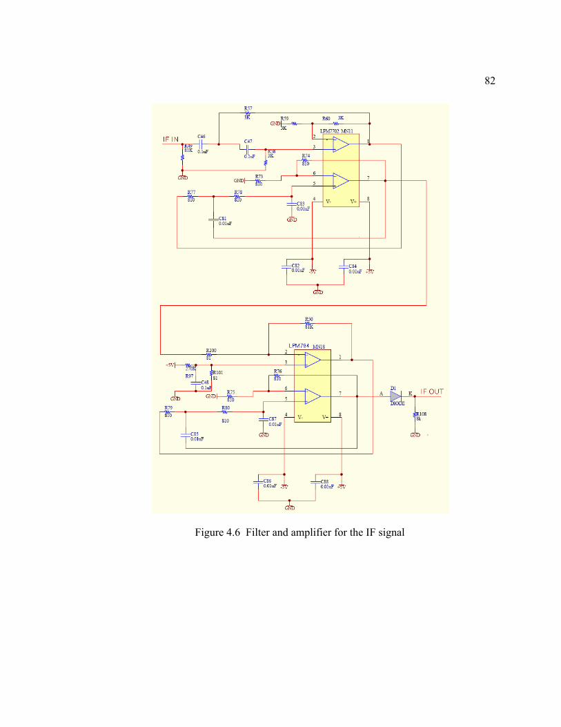
82
Figure 4.6 Filter and amplifier for the IF signal
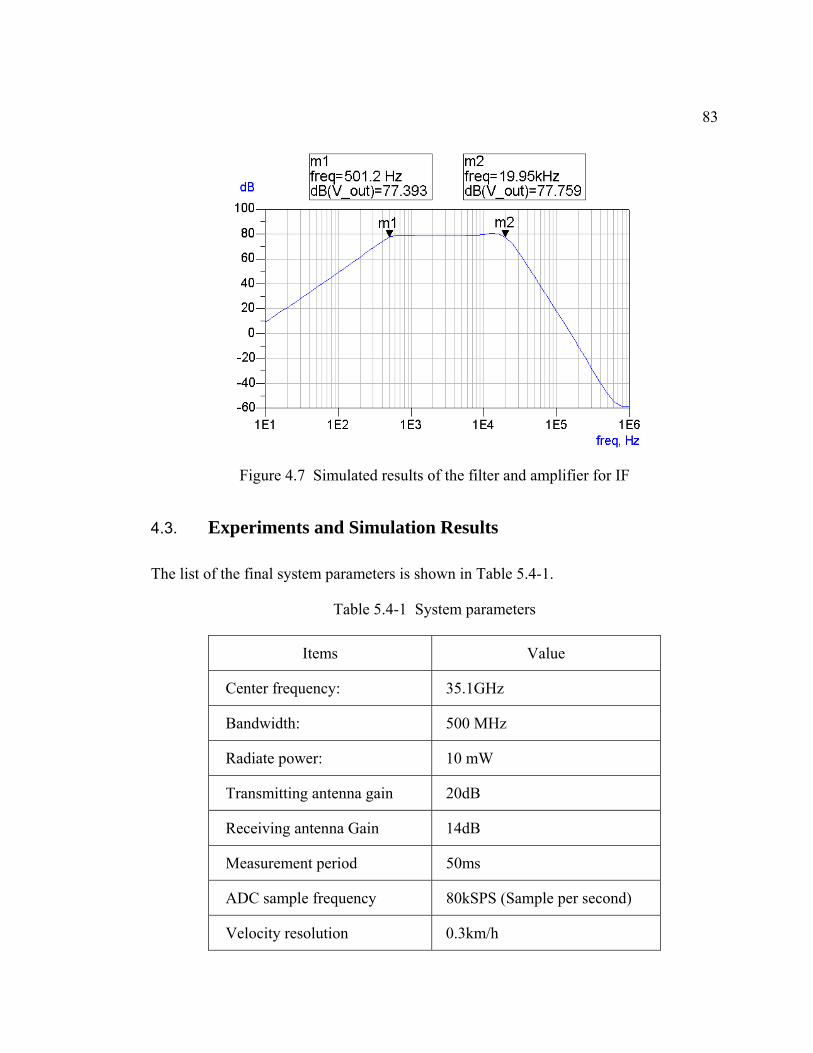
83
Figure 4.7 Simulated results of the filter and amplifier for IF
4.3. Experiments and Simulation Results
The list of the final system parameters is shown in Table 5.4-1.
Table 5.4-1 System parameters
Items Value
Center frequency: 35.1GHz
Bandwidth: 500 MHz
Radiate power: 10 mW
Transmitting antenna gain 20dB
Receiving antenna Gain 14dB
Measurement period 50ms
ADC sample frequency 80kSPS (Sample per second)
Velocity resolution 0.3km/h
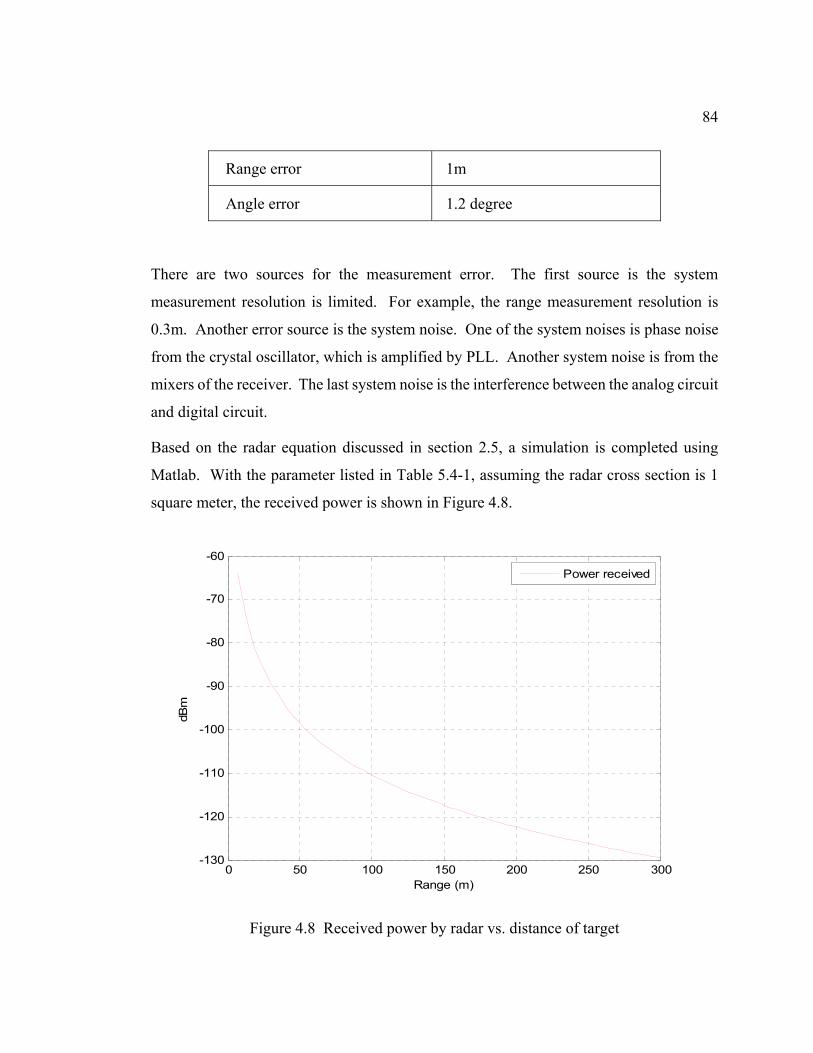
84
Range error 1m
Angle error 1.2 degree
There are two sources for the measurement error. The first source is the system
measurement resolution is limited. For example, the range measurement resolution is
0.3m. Another error source is the system noise. One of the system noises is phase noise
from the crystal oscillator, which is amplified by PLL. Another system noise is from the
mixers of the receiver. The last system noise is the interference between the analog circuit
and digital circuit.
Based on the radar equation discussed in section 2.5, a simulation is completed using
Matlab. With the parameter listed in Table 5.4-1, assuming the radar cross section is 1
square meter, the received power is shown in Figure 4.8.
Figure 4.8 Received power by radar vs. distance of target
0 50 100 150 200 250 300-130
-120
-110
-100
-90
-80
-70
-60
Range (m)
dBm
Power received
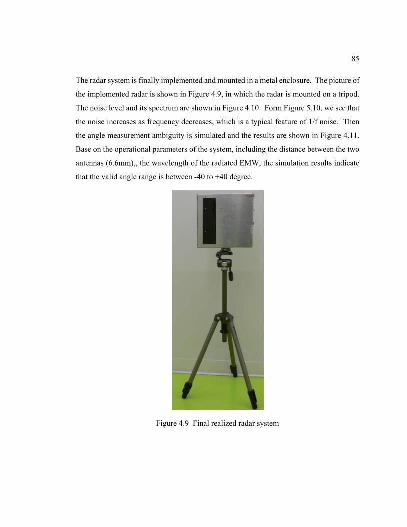
85
The radar system is finally implemented and mounted in a metal enclosure. The picture of
the implemented radar is shown in Figure 4.9, in which the radar is mounted on a tripod.
The noise level and its spectrum are shown in Figure 4.10. Form Figure 5.10, we see that
the noise increases as frequency decreases, which is a typical feature of 1/f noise. Then
the angle measurement ambiguity is simulated and the results are shown in Figure 4.11.
Base on the operational parameters of the system, including the distance between the two
antennas (6.6mm),, the wavelength of the radiated EMW, the simulation results indicate
that the valid angle range is between -40 to +40 degree.
Figure 4.9 Final realized radar system
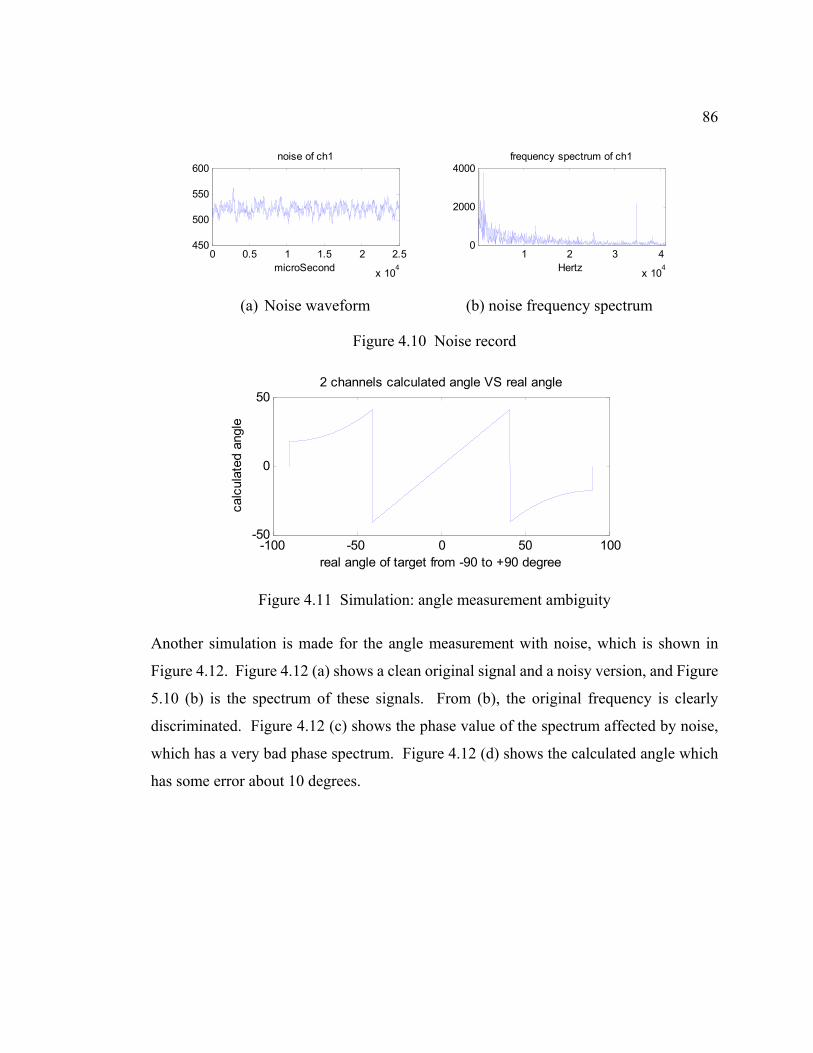
86
(a) Noise waveform (b) noise frequency spectrum
Figure 4.10 Noise record
Figure 4.11 Simulation: angle measurement ambiguity
Another simulation is made for the angle measurement with noise, which is shown in
Figure 4.12. Figure 4.12 (a) shows a clean original signal and a noisy version, and Figure
5.10 (b) is the spectrum of these signals. From (b), the original frequency is clearly
discriminated. Figure 4.12 (c) shows the phase value of the spectrum affected by noise,
which has a very bad phase spectrum. Figure 4.12 (d) shows the calculated angle which
has some error about 10 degrees.
0 0.5 1 1.5 2 2.5
x 104
450
500
550
600
microSecond
noise of ch1
1 2 3 4
x 104
0
2000
4000
Hertz
frequency spectrum of ch1
-100 -50 0 50 100-50
0
502 channels calculated angle VS real angle
real angle of target from -90 to +90 degree
cal
cula
ted
angl
e
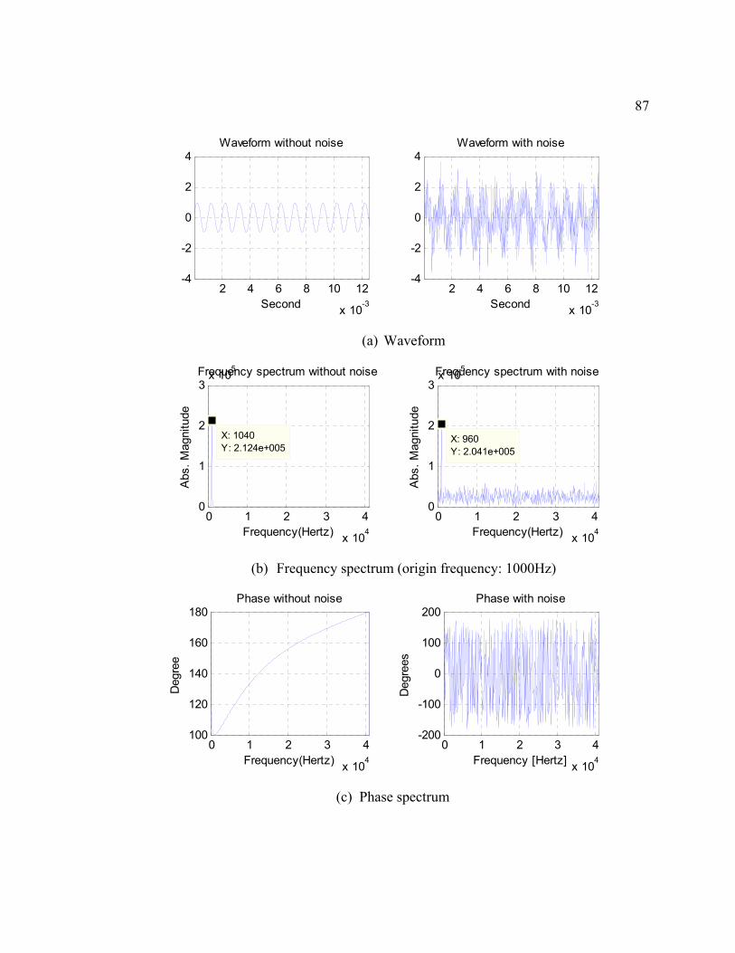
87
(a) Waveform
(b) Frequency spectrum (origin frequency: 1000Hz)
(c) Phase spectrum
2 4 6 8 10 12
x 10-3
-4
-2
0
2
4Waveform without noise
Second2 4 6 8 10 12
x 10-3
-4
-2
0
2
4Waveform with noise
Second
0 1 2 3 4
x 104
0
1
2
3x 10⁵
X: 1040Y: 2.124e+005
Abs
. Mag
nitu
de
Frequency(Hertz)
Frequency spectrum without noise
0 1 2 3 4
x 104
0
1
2
3x 10⁵
Abs
. Mag
nitu
de
Frequency(Hertz)
Frequency spectrum with noise
X: 960Y: 2.041e+005
0 1 2 3 4
x 104
100
120
140
160
180Phase without noise
Frequency(Hertz)
Deg
ree
0 1 2 3 4
x 104
-200
-100
0
100
200
Deg
rees
Frequency [Hertz]
Phase with noise
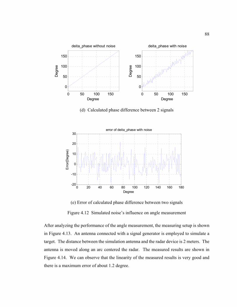
88
(d) Calculated phase difference between 2 signals
(e) Error of calculated phase difference between two signals
Figure 4.12 Simulated noise’s influence on angle measurement
After analyzing the performance of the angle measurement, the measuring setup is shown
in Figure 4.13. An antenna connected with a signal generator is employed to simulate a
target. The distance between the simulation antenna and the radar device is 2 meters. The
antenna is moved along an arc centered the radar. The measured results are shown in
Figure 4.14. We can observe that the linearity of the measured results is very good and
there is a maximum error of about 1.2 degree.
0 50 100 150
0
50
100
150
deita_phase without noise
Degree
Deg
ree
0 50 100 150
0
50
100
150
deita_phase with noise
Degree
Deg
ree
0 20 40 60 80 100 120 140 160 180-20
-10
0
10
20
30error of deita_phase with noise
Degree
Erro
r(Deg
ree)
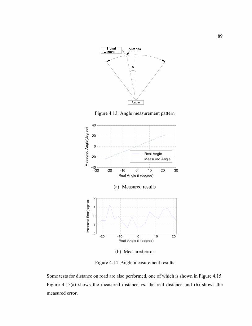
89
Figure 4.13 Angle measurement pattern
(a) Measured results
(b) Measured error
Figure 4.14 Angle measurement results
Some tests for distance on road are also performed, one of which is shown in Figure 4.15.
Figure 4.15(a) shows the measured distance vs. the real distance and (b) shows the
measured error.
-30 -20 -10 0 10 20 30-40
-20
0
20
40
Real Angle θ (degree)
Mea
sure
d A
ngle
(deg
ree)
Real AngleMeasured Angle
-20 -10 0 10 20-2
-1
0
1
2
Real Angle θ (degree)
Mea
sure
d E
rror(d
egre
e)
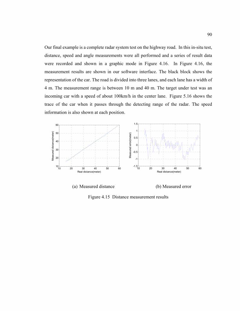
90
Our final example is a complete radar system test on the highway road. In this in-situ test,
distance, speed and angle measurements were all performed and a series of result data
were recorded and shown in a graphic mode in Figure 4.16. In Figure 4.16, the
measurement results are shown in our software interface. The black block shows the
representation of the car. The road is divided into three lanes, and each lane has a width of
4 m. The measurement range is between 10 m and 40 m. The target under test was an
incoming car with a speed of about 100km/h in the center lane. Figure 5.16 shows the
trace of the car when it passes through the detecting range of the radar. The speed
information is also shown at each position.
(a) Measured distance (b) Measured error
Figure 4.15 Distance measurement results
10 20 30 40 50 6010
20
30
40
50
60
Real distance(meter)
Mea
sure
d di
stan
ce(m
eter
)
10 20 30 40 50 60-1.5
-1
-0.5
0
0.5
1
1.5
Real distance(meter)
Mea
sure
d er
ror(m
eter
)
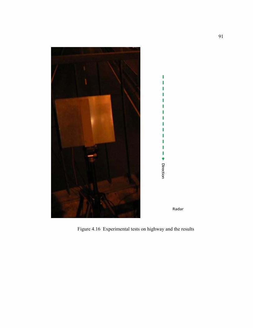
91
Radar
Direction
Figure 4.16 Experimental tests on highway and the results
92
CHAPTER 5 CONCLUSION AND FUTURE WORK
5.1. Conclusion
In this thesis, a software-defined-radar system based on the frequency synthesis and the
digital signal processing techniques has been analyzed, developed and fabricated. A
series of simulations and measurements were made which has verified the performances
and functionalities of the proposed system.
The whole system mainly consists of four parts: the frequency synthesizer, the transceiver
frond-end, the IF filter and amplifier circuits and the digital signal processing system.
These parts are already integrated into a single platform which can work as an integrated
prototype. Measurement results show that the system has the capacity to measure the
speed, distance and relative angle of a target in case that the moving direction is known.
To integrate the CW and FMCW frequency sweeps together, DDS and PLL are employed
in the system. The performance and characteristics of the frequency synthesizer system
are analyzed and simulated. In order to achieve planarization and miniaturization, planar
SIW antennas are used. To realize the angle measurement, dual receiving antennas and
dual receivers are used in this system. The angle measurement ambiguity function of the
dual antenna system is analyzed through simulation results.
Hardware of the DSP system on board was implemented based on the ARM core, in
which the DSP algorithm based on FFT is realized. Certain functions of radar system are
implemented and verified by the software. Finally, this system is able to measure the
range, speed and angle of target such as automobile monitoring.
However, some difficulties bring down the performance and functionalities of the system.
One of them is the multi-target problem and the moving direction ambiguity mentioned in
sections 2.6 and 6.2, respectively. The angle measurement ambiguity and accuracy
present another problem to be resolved.
93
5.2. Future Work
In the real environment, multi-target cases are most often encountered and they are
supposed to be measured. Therefore, the multi-target ambiguity is a main subject to be
resolved. To resolve this difficulty, a range Doppler algorithm should be implemented for
multi-target applications.
In order to realize more advanced algorithm, computational power of the DSP system
should be improved too. Other DSP technologies such dedicated DSP and FPGA are
possible candidates.
The accuracy of the current system is not high enough to work in some specific scenarios
that need measurements with a very high resolution. Further study should be done for
improving the measurement accuracy.
94
REFERENCE
[1] Ke Wu, Dominic Deslandes, and Yves Cassivi, “The Substrate Integrated Circuits -
A New Concept for High-Frequency Electronics and Optoelectronics”,
Mikrotalasna revija, December 2003.
[2] Hui Zhang, “Software Defined Radar System”, École Polytechnique de Montréal,
2007
[3] Hui Zhang, Lin Li, Ke Wu, “Software-Defined Six-Port Radar Technique for
Precision
[4] Wipro Technologies, “Software-Defined Radio White Paper, A Technology
Overview”, Wipro Technologies, 2002
[5] Harold R. Raemer, “Radar system Principles”, CRC Press, Inc., 1997
[6] M.I. Skolnik, “Introduction to radar systems”, Chapter1.2, McGraw Hill, 2001.
[7] R.D. Kuhne, “From vision to reality Mobile communication application for traffic
control and traffic management,’’ ITST 2002, Seoul, Korea.
[8] L. H. Eriksson and S. Brodén, “High performance automotive radar,” Microwave J.,
pp. 24–38, Oct. 1996.
[9] Intelligent Automation Inc., “Software defined radar”, [online],
http://www.i-a-i.com/
[10] M. Jankiraman, “Design of Multi-Frequency CW Radars”, Raleigh, N.C.: Scitech
Publishing, 2007.
[11] Analog Device Inc, “Datasheet of AD9854”, [online]: http://www.analog.com,
Analog Device Inc., 2008.
[12] Analog Device Inc, “Datasheet of ADF4108”, [online]: http://www.analog.com,
Analog Device Inc., 2008.
95
[13] Atmel Corporation, “Datasheet of AT91SAM7xxx ”, [online]:
http://www.atmel.com, Atmel Corporation, 2008.
[14] Hittite Microwave Corporation, “Datasheet of HMC-ALH369” [online],
www.hittite.com, Hittite Microwave Corporation, 2008.
[15] Hittite Microwave Corporation, “Datasheet of HMC329” [online], www.hittite.com,
Hittite Microwave Corporation, 2008.
[16] Hittite Microwave Corporation, “Datasheet of HMC582LP5 / 582LP5E” [online],
www.hittite.com, Hittite Microwave Corporation, 2008.
[17] TriQuint Semiconductor, “Datasheet of TGA4036” [online], www.triquint.com,
Hittite TriQuint Semiconductor, 2008
[18] TriQuint Semiconductor, “Datasheet of TGC1430G-EPU” [online],
www.triquint.com, Hittite TriQuint Semiconductor, 2008
[19] J. Robert Jensen , “Angle Measurement with a Phase Monopulse Radar Altimeter”
IEEE TRANSACTIONS ON ANTENNAS AND PROPAGATION, VOL. 47, NO.
4, APRIL 1999.
[20] Range Measurements”, IEEE SENSORS JOURNAL, VOL. 8, NO. 10, OCTOBER
2008.
[21] J. Webster (ed.), “Wiley Encyclopedia of Electrical and Electronics Engineering”,
Part “Frequency synthesis” , John Wiley & Sons, Inc., 1999.
[22] Roland E. Best, “Phase locked loops design, simulation, &applications”, Chapter1,
Chapter2,
[23] Wikipedia, “RS-232” [online], http://en.wikipedia.org/wiki/Rs232
[24] Wikipedia, “EIA-485” [online], http://en.wikipedia.org/wiki/EIA-485
[25] Eyung W. Kang, “Radar System analysis, design, and simulation”, ARTECH
OUSE, INC. 2008
96
[26] Douglas L. Jones , “Decimation-in-time (DIT) Radix-2 FFT” [online],
http://cnx.org /content/m12016/latest/
[27] Vijayk.Jain, William L.Collins, JR., and David C. Davis, “High-Accuracy Analog
Measurements via Interpolated FFT”, IEEE TRANSACTIONS ON INSTRUMEN-
TATION AND MEASUREMENT, VOL. IM-28, NO. 2, JUNE 1979
[28] Winfried Mayer, Member, IEEE, Martin Meilchen,Wilfried Grabherr, Member,
IEEE, Peter Nüchter, and Rainer Gühl, “Eight-Channel 77-GHz Front-End Module
With High-Performance Synthesized Signal Generator for FM-CW Sensor
Applications”, IEEE TRANSACTIONS ON MICROWAVE THEORY AND
TECHNIQUES, VOL. 52, NO. 3, MARCH 2004
[29] Analog Device, “A Technical Tutorial on Digital Signal Synthesis”, Analog Device
Inc., 1999,
[30] Maxim Inc., “Clock (CLK) Jitter and Phase Noise Conversion”, application note
3359 Maxim Inc,. 2004
[31] Wikipedia: “Universal Serial Bus”, [online], http://en.wikipedia.org /wiki/Usb


![Radio Frequency Identification [JePartage]](https://img.pdfslide.fr/doc/110x75/5a6533127f8b9a5b558b521d/radio-frequency-identification-jepartage.jpg)