Embed Size (px)
Citation preview
Rapport Technique RT/PBS8219.1.1.30.010.300.070
Date création : 10/08/2007
RT Module mesure IV pour émittancemètres LBE/LME Page 1 sur 31
Rédacteur Vérificateur Approbateurs
Rapport Technique Module mesure IV pour Emittancemètres lignes LBE/LME
Nom CH. OLIVETTO Nom M. ROUSSEAU Nom P. AUSSET
Tél. 03 88 10 65 80 Tél. 03 88 10 64 58 Tél. 01 69 15 81 61
Courriel [email protected] Courriel [email protected]
Courriel [email protected]
Fonction Coordinateur Technique Fonction Responsable Scientifique Fonction Responsable Diagnostics
Date 18/07/2008 Date 18/07/2008 Date
Visa Visa Visa Ce document est la copropriété du CEA/CNRS. Il ne peut être reproduit ou diffusé sans l’autorisation de l’équipe direction de projet SPIRAL2.
SP2_MD_8111_I009651V1.0
Reference Spiral2 réduite
RT Module mesure IVT pour émittancemètre LBE/LME
Page 2 sur 31
Ce document est la copropriété du CEA/CNRS. Il ne peut être reproduit ou diffusé sans l’autorisation de l’équipe direction de projet SPIRAL2.
HISTORIQUE DES MODIFICATIONS
Version Date Pages modifiées Motifs Version 1.0 18/07/2008 Version originale LISTE DE DIFFUSION
Interne Externe Documentation Associée
Lien Commentaires https://edms.in2p3.fr/document/I-010070/1
Plan de développement des émittancemètres LBE https://edms.in2p3.fr/document/I-010532/2
Rapport Fonctionnel de l’Interface Homme Machine pour le BTI et les émittancemètres LBE/LME
http://ireswww.in2p3.fr/spiral2/PBS/index.php Site WEB PBS traçabilité des objets
Reference Spiral2 réduite
RT Module mesure IVT pour émittancemètre LBE/LME
Page 3 sur 31
Ce document est la copropriété du CEA/CNRS. Il ne peut être reproduit ou diffusé sans l’autorisation de l’équipe direction de projet SPIRAL2.
Vérificateur :
Date :
Commentaires :
Reference Spiral2 réduite
RT Module mesure IVT pour émittancemètre LBE/LME
Page 4 sur 31
Ce document est la copropriété du CEA/CNRS. Il ne peut être reproduit ou diffusé sans l’autorisation de l’équipe direction de projet SPIRAL2.
Approbateur :
Date :
Commentaires :
Reference Spiral2 réduite
RT Module mesure IVT pour émittancemètre LBE/LME
Page 5 sur 31
Ce document est la copropriété du CEA/CNRS. Il ne peut être reproduit ou diffusé sans l’autorisation de l’équipe direction de projet SPIRAL2.
SOMMAIRE 1. ................................................................................................... 7 Objet du document2. ........................................................................................... 7 Présentation du produit
Le contexte technique....................................................................................................................... 7 Les objectifs scientifiques de l’équipement.................................................................................... 8
2.1.1. ...................................................................................................................... 8 Rappel sur la notion d’émittance2.1.2. ................................................................................................................................... 10 Principe de l’émittance
Les performances principales de l’instrument ............................................................................. 12 La description des principaux sous-ensembles ........................................................................... 13
3. ............ 15 Descriptif du Module de mesureIV pour émittancemètres LBE et LME4. ........................................................... 17 Installation et configuration du module IV5. ........................................................................... 18 Descriptif technique du matériel6. ............................................................................. 19 Entrées/Sorties et connectique7. ..................................... 20 Caractéristiques liées à la sécurité de fonctionnement8. ........................................................................................... 21 Interfaces Mécaniques
Interfaces mécaniques .................................................................................................................... 21 8.1.1. ................................................................................................................ 21 Description du concept mécanique8.1.2. ...................................................................................................................................... 21 Plan de la face avant8.1.3. ...................................................................................................................................... 22 Repérage du produit
9. ........................................................................................... 23 Dossier de FabricationNomenclatures Composants .......................................................................................................... 24 Circuit imprimé principal ................................................................................................................ 25
10. .................................................................................................... 26 Tests et MesuresAnnexes : Datasheet principaux composants ............................................................ 31
Reference Spiral2 réduite
RT Module mesure IVT pour émittancemètre LBE/LME
Page 6 sur 31
Ce document est la copropriété du CEA/CNRS. Il ne peut être reproduit ou diffusé sans l’autorisation de l’équipe direction de projet SPIRAL2.
Liste des Figures Figure 1: Découpage en bloc fonctionnel de la chaine d'acquisition émittancemètre. .............. 8 Figure 2 : Définition des coordonnées des particules ................................................................ 8 Figure 3: Différentes figures théoriques d'émittance ................................................................. 9 Figure 4: Schéma de principe de l'émittancemètre................................................................... 11 Figure 5: Dessin d'un émittancemètre avec la tête de mesure mobile...................................... 12 Figure 6: Blocs fonctionnels par couple d'émittancemètre ...................................................... 13 Figure 7: Localisation des baies électroniques liées aux émittancemètres .............................. 14 Figure 8: Synoptique mesure et acquisition des courants des têtes des émittancemètres ........ 15 Figure 9: Face avant module IV avec entrées/sorties............................................................... 16 Figure 10: Vue de la carte IV coté composants ....................................................................... 17 Figure 11: Vue de la carte IV coté soudure.............................................................................. 18 Figure 12: Configuration matériel choix alimentation des optocoupleurs............................... 18 Figure 13: Synoptique du module de conversion courant/tension ........................................... 19 Figure 14: Schéma fonctionnel des interfaces logiques pour les gains et les courants tests du module I/V................................................................................................................................ 20 Figure 15: Vue éclatée et monté du module blindé Schroff..................................................... 21 Figure 16: Mesures de courant sur module LBE1 N°1 ............................................................ 26 Figure 17: Mesures de courant sur module LBE1 N°2 ............................................................ 27 Figure 18: Mesures de courant sur module LBEC N°1 ........................................................... 27 Figure 19: Mesures courant sur module LBEC N°2 ................................................................ 28 Figure 20: Mesures de courant sur module LME N°1 ............................................................. 28 Figure 21: Mesures de courant sur module LME N°2 ............................................................. 29 Tableaux
Reference Spiral2 réduite
RT Module mesure IVT pour émittancemètre LBE/LME
Page 7 sur 31
Ce document est la copropriété du CEA/CNRS. Il ne peut être reproduit ou diffusé sans l’autorisation de l’équipe direction de projet SPIRAL2.
1. Objet du document Le Rapport Technique du module de mesure IV (conversion courant-tension) reprend l’ensemble des informations techniques liées à cet équipement dans le but de : - Comprendre tous les détails techniques de cet équipement électronique - Pouvoir dépanner le cas échéant cet équipement - Le faire fabriquer auprès d’une société extérieure - Regrouper l’ensemble des données technique des différents composants électroniques intégrés dans cet équipement. - Regrouper les informations de contrôle et commande le cas échéant. - Décrire l’ensemble des tests et mesures ayant permit la réception de ces équipements. Il est figé et formellement approuvé par le responsable produit et l’ingénieur système gérant le niveau supérieur à la fin de la phase itérative de sa rédaction. Il est ensuite géré en configuration.
2. Présentation du produit
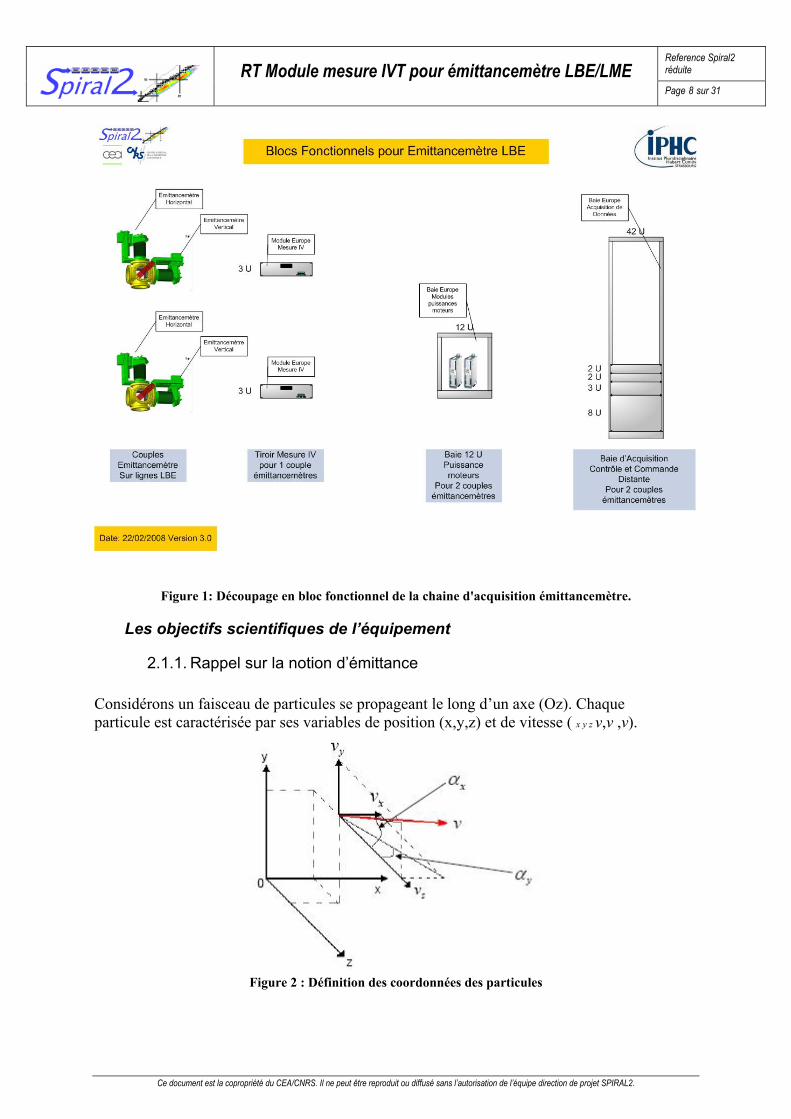
Le contexte technique Le module de mesure IV rentre dans la chaîne globale d’acquisition des diagnostics émittancemètres des lignes LBE du projet Spiral2 et permet la conversion courant-tension issu de la cage da faraday de la tête de mesure interceptant le faisceau à analyser.. Les diagnostics Emittancemètre, basés sur le principe scanner type ALLISSON, seront intégrés sur les lignes d’injection du projet SPIRAL2. Ils seront intégrés en couple un émittancemètre par plan (Horizontal et Vertical), chaque émittancemètre sera composé d’un ensemble mécanique de translation comportant une partie mobile actionnée par un moteur via une vis. Un tiroir intermédiaire intègrera les modules de conversion courant/tension ainsi que les amplificateurs de lecture des thermocouples intégrés sur les écrans thermique des têtes de mesures des émittancemètres. Une baie intermédiaire locale incorporera les modules de puissance pour les moteurs Une baie d’acquisition finale intégrera l’ensemble des modules, cartes et châssis formant le système complet d’acquisition et de traitement de l’information issue des deux émittancemètre. Cette baie sera déportée hors de la zone protégée de l’accélérétateur. La figure ci-dessous reprend ce découpage :
Reference Spiral2 réduite
RT Module mesure IVT pour émittancemètre LBE/LME
Page 8 sur 31
Ce document est la copropriété du CEA/CNRS. Il ne peut être reproduit ou diffusé sans l’autorisation de l’équipe direction de projet SPIRAL2.
Figure 1: Découpage en bloc fonctionnel de la chaine d'acquisition émittancemètre.
Les objectifs scientifiques de l’équipement
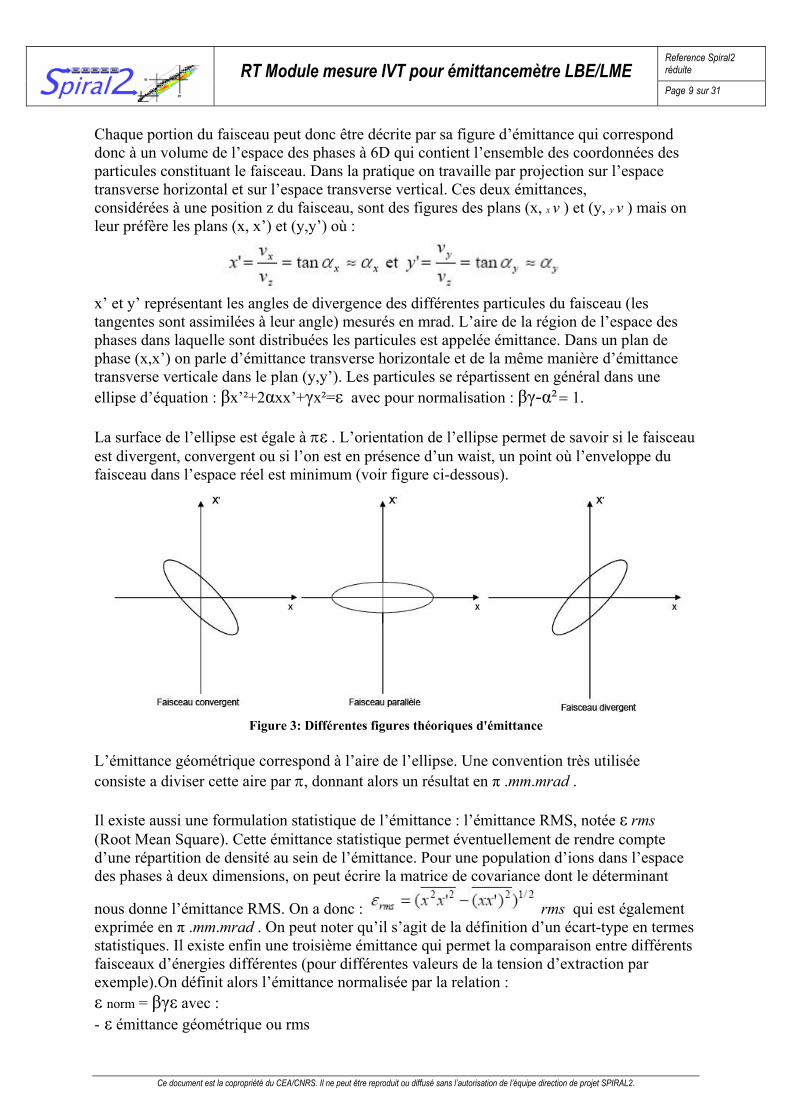
2.1.1. Rappel sur la notion d’émittance Considérons un faisceau de particules se propageant le long d’un axe (Oz). Chaque particule est caractérisée par ses variables de position (x,y,z) et de vitesse ( x y z v,v ,v).
Figure 2 : Définition des coordonnées des particules
Reference Spiral2 réduite
RT Module mesure IVT pour émittancemètre LBE/LME
Page 9 sur 31
Ce document est la copropriété du CEA/CNRS. Il ne peut être reproduit ou diffusé sans l’autorisation de l’équipe direction de projet SPIRAL2.
Chaque portion du faisceau peut donc être décrite par sa figure d’émittance qui correspond donc à un volume de l’espace des phases à 6D qui contient l’ensemble des coordonnées des particules constituant le faisceau. Dans la pratique on travaille par projection sur l’espace transverse horizontal et sur l’espace transverse vertical. Ces deux émittances, considérées à une position z du faisceau, sont des figures des plans (x, x v ) et (y, y v ) mais on leur préfère les plans (x, x’) et (y,y’) où :
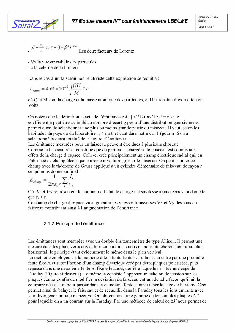
x’ et y’ représentant les angles de divergence des différentes particules du faisceau (les tangentes sont assimilées à leur angle) mesurés en mrad. L’aire de la région de l’espace des phases dans laquelle sont distribuées les particules est appelée émittance. Dans un plan de phase (x,x’) on parle d’émittance transverse horizontale et de la même manière d’émittance transverse verticale dans le plan (y,y’). Les particules se répartissent en général dans une ellipse d’équation : βx’²+2αxx’+γx²=ε avec pour normalisation : βγ-α² = 1. La surface de l’ellipse est égale à πε . L’orientation de l’ellipse permet de savoir si le faisceau est divergent, convergent ou si l’on est en présence d’un waist, un point où l’enveloppe du faisceau dans l’espace réel est minimum (voir figure ci-dessous).
Figure 3: Différentes figures théoriques d'émittance
L’émittance géométrique correspond à l’aire de l’ellipse. Une convention très utilisée consiste a diviser cette aire par π, donnant alors un résultat en π .mm.mrad . Il existe aussi une formulation statistique de l’émittance : l’émittance RMS, notée ε rms (Root Mean Square). Cette émittance statistique permet éventuellement de rendre compte d’une répartition de densité au sein de l’émittance. Pour une population d’ions dans l’espace des phases à deux dimensions, on peut écrire la matrice de covariance dont le déterminant
nous donne l’émittance RMS. On a donc : rms qui est également exprimée en π .mm.mrad . On peut noter qu’il s’agit de la définition d’un écart-type en termes statistiques. Il existe enfin une troisième émittance qui permet la comparaison entre différents faisceaux d’énergies différentes (pour différentes valeurs de la tension d’extraction par exemple).On définit alors l’émittance normalisée par la relation : ε norm = βγε avec : - ε émittance géométrique ou rms
Reference Spiral2 réduite
RT Module mesure IVT pour émittancemètre LBE/LME
Page 10 sur 31
Ce document est la copropriété du CEA/CNRS. Il ne peut être reproduit ou diffusé sans l’autorisation de l’équipe direction de projet SPIRAL2.
- Les deux facteurs de Lorentz - Vz la vitesse radiale des particules - c la célérité de la lumière Dans le cas d’un faisceau non relativiste cette expression se réduit à :
où Q et M sont la charge et la masse atomique des particules, et U la tension d’extraction en Volts. On notera que la définition exacte de l’émittance est : βx’²+2αxx’+γx² = nε ; le coefficient n peut être assimilé au nombre d’écart-types σ d’une distribution gaussienne et permet ainsi de sélectionner une plus ou moins grande partie du faisceau. Il vaut, selon les habitudes du pays ou du laboratoire 1, 4 ou 6 et vaut dans notre cas 1 (pour n=6 on a sélectionné la quasi totalité de la figure d’émittance Les émittance mesurées pour un faisceau peuvent être dues à plusieurs choses : Comme le faisceau n’est constitué que de particules chargées, le faisceau est soumis aux effets de la charge d’espace. Celle-ci crée principalement un champ électrique radial qui, en l’absence de champ électrique correcteur va faire grossir le faisceau. On peut estimer ce champ avec le théorème de Gauss appliqué à un cylindre élémentaire de faisceau de rayon r ce qui nous donne au final :
Où Ii et Vzi représentent le courant de l’état de charge i et savitesse axiale correspondante tel que ri < r. Ce champ de charge d’espace va augmenter les vitesses transverses Vx et Vy des ions du faisceau contribuant ainsi à l’augmentation de l’émittance.
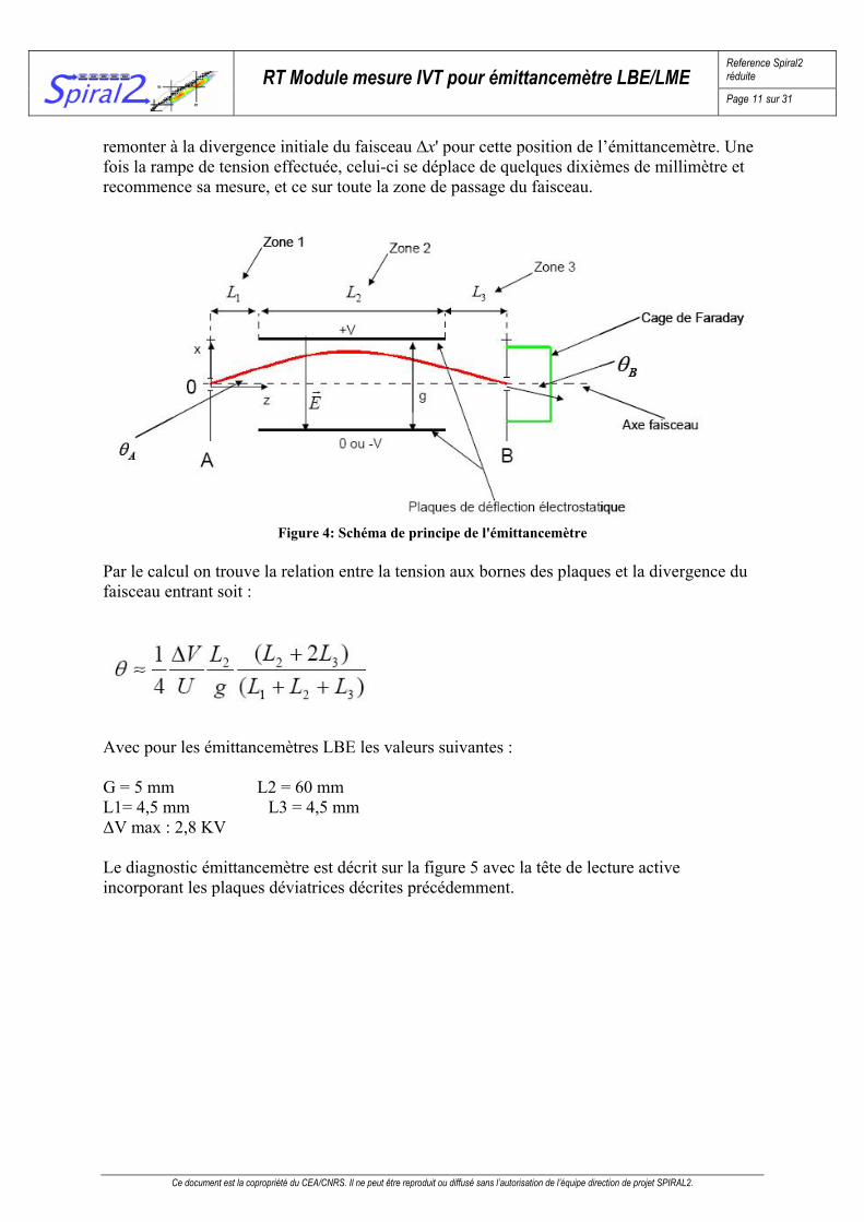
2.1.2. Principe de l’émittance Les émittances sont mesurées avec un double émittancemètre de type Allison. Il permet une mesure dans les plans verticaux et horizontaux mais nous ne nous attacherons ici qu’au plan horizontal, le principe étant évidemment le même dans le plan vertical. La méthode employée est la méthode dite « fente-fente ». Le faisceau entre par une première fente fixe A et subit l’action d’un champ électrique créé par deux plaques polarisées, puis repasse dans une deuxième fente B, fixe elle aussi, derrière laquelle se situe une cage de Faraday (Figure ci-dessous). La méthode consiste à apposer un échelon de tension sur les plaques centrales afin de modifier la déviation du faisceau entrant de telle façon qu’il ait la courbure nécessaire pour passer dans la deuxième fente et ainsi taper la cage de Faraday. Ceci permet ainsi de balayer le faisceau et de recueillir dans la Faraday tous les ions entrants avec leur divergence initiale respective. On obtient ainsi une gamme de tension des plaques ΔV pour laquelle on a un courant sur la Faraday. Par une méthode de calcul ce ΔV nous permet de
Reference Spiral2 réduite
RT Module mesure IVT pour émittancemètre LBE/LME
Page 11 sur 31
Ce document est la copropriété du CEA/CNRS. Il ne peut être reproduit ou diffusé sans l’autorisation de l’équipe direction de projet SPIRAL2.
remonter à la divergence initiale du faisceau Δx' pour cette position de l’émittancemètre. Une fois la rampe de tension effectuée, celui-ci se déplace de quelques dixièmes de millimètre et recommence sa mesure, et ce sur toute la zone de passage du faisceau.
Figure 4: Schéma de principe de l'émittancemètre
Par le calcul on trouve la relation entre la tension aux bornes des plaques et la divergence du faisceau entrant soit :
Avec pour les émittancemètres LBE les valeurs suivantes : G = 5 mm L2 = 60 mm L1= 4,5 mm L3 = 4,5 mm ΔV max : 2,8 KV Le diagnostic émittancemètre est décrit sur la figure 5 avec la tête de lecture active incorporant les plaques déviatrices décrites précédemment.
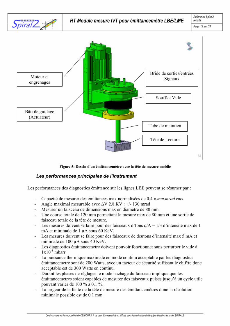
Reference Spiral2 réduite
RT Module mesure IVT pour émittancemètre LBE/LME
Page 12 sur 31
Ce document est la copropriété du CEA/CNRS. Il ne peut être reproduit ou diffusé sans l’autorisation de l’équipe direction de projet SPIRAL2.
Moteur et engrenages
Bride de sorties/entrées Signaux
Bâti de guidage (Actuateur)
Tube de maintien
Soufflet Vide
Tête de Lecture
Figure 5: Dessin d'un émittancemètre avec la tête de mesure mobile
Les performances principales de l’instrument Les performances des diagnostics émittance sur les lignes LBE peuvent se résumer par :
- Capacité de mesurer des émittances max normalisées de 0.4 π.mm.mrad rms. - Angle maximal mesurable avec ΔV 2,8 KV : +/- 130 mrad - Mesurer un faisceau de dimensions max en diamètre de 80 mm - Une course totale de 120 mm permettant la mesure max de 80 mm et une sortie de
faisceau totale de la tête de mesure. - Les mesures doivent se faire pour des faisceaux d’Ions q/A = 1/3 d’intensité max de 1
mA et minimale de 1 µA sous 60 KeV. - Les mesures doivent se faire pour des faisceaux de deutons d’intensité max 5 mA et
minimale de 100 µA sous 40 KeV. - Les diagnostics émittancemètre doivent pouvoir fonctionner sans perturber le vide à
1x10⁻⁸ mbarr. - La puissance thermique maximale en mode continu acceptable par les diagnostics
émittancemètre sont de 200 Watts, avec un facteur de sécurité suffisant le chiffre donc acceptable est de 300 Watts en continu.
- Durant les phases de réglages le mode hachage du faisceau implique que les émittancemètres soient capables de mesurer des faisceaux pulsés jusqu’à un cycle utile pouvant varier de 100 % à 0.1 %.
- La largeur de la fente de la tête de mesure des émittancemètres donc la résolution minimale possible est de 0.1 mm.
Reference Spiral2 réduite
RT Module mesure IVT pour émittancemètre LBE/LME
Page 13 sur 31
Ce document est la copropriété du CEA/CNRS. Il ne peut être reproduit ou diffusé sans l’autorisation de l’équipe direction de projet SPIRAL2.
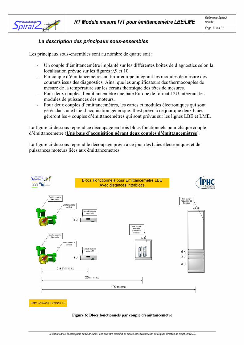
La description des principaux sous-ensembles Les principaux sous-ensembles sont au nombre de quatre soit :
- Un couple d’émittancemètre implanté sur les différentes boites de diagnostics selon la localisation prévue sur les figures 9,9 et 10.
- Par couple d’émittancemètres un tiroir europe intégrant les modules de mesure des courants issus des diagnostics. Ainsi que les amplificateurs des thermocouples de mesure de la température sur les écrans thermique des têtes de mesures.
- Pour deux couples d’émittancemètre une baie Europe de format 12U intégrant les modules de puissances des moteurs.
- Pour deux couples d’émittancemètres, les cartes et modules électroniques qui sont gérés dans une baie d’acquisition générique. Il est prévu à ce jour que deux baies géreront les 4 couples d’émittancemètres qui sont prévus sur les lignes LBE et LME.
La figure ci-dessous reprend ce découpage en trois blocs fonctionnels pour chaque couple d’émittancemètre (Une baie d’acquisition gérant deux couples d’émittancemètres). La figure ci-dessous reprend le découpage prévu à ce jour des baies électroniques et de puissances moteurs liées aux émittancemètres.
Figure 6: Blocs fonctionnels par couple d'émittancemètre
Reference Spiral2 réduite
RT Module mesure IVT pour émittancemètre LBE/LME
Page 14 sur 31
Ce document est la copropriété du CEA/CNRS. Il ne peut être reproduit ou diffusé sans l’autorisation de l’équipe direction de projet SPIRAL2.
Figure 7: Localisation des baies électroniques liées aux émittancemètres
Reference Spiral2 réduite
RT Module mesure IVT pour émittancemètre LBE/LME
Page 15 sur 31
Ce document est la copropriété du CEA/CNRS. Il ne peut être reproduit ou diffusé sans l’autorisation de l’équipe direction de projet SPIRAL2.
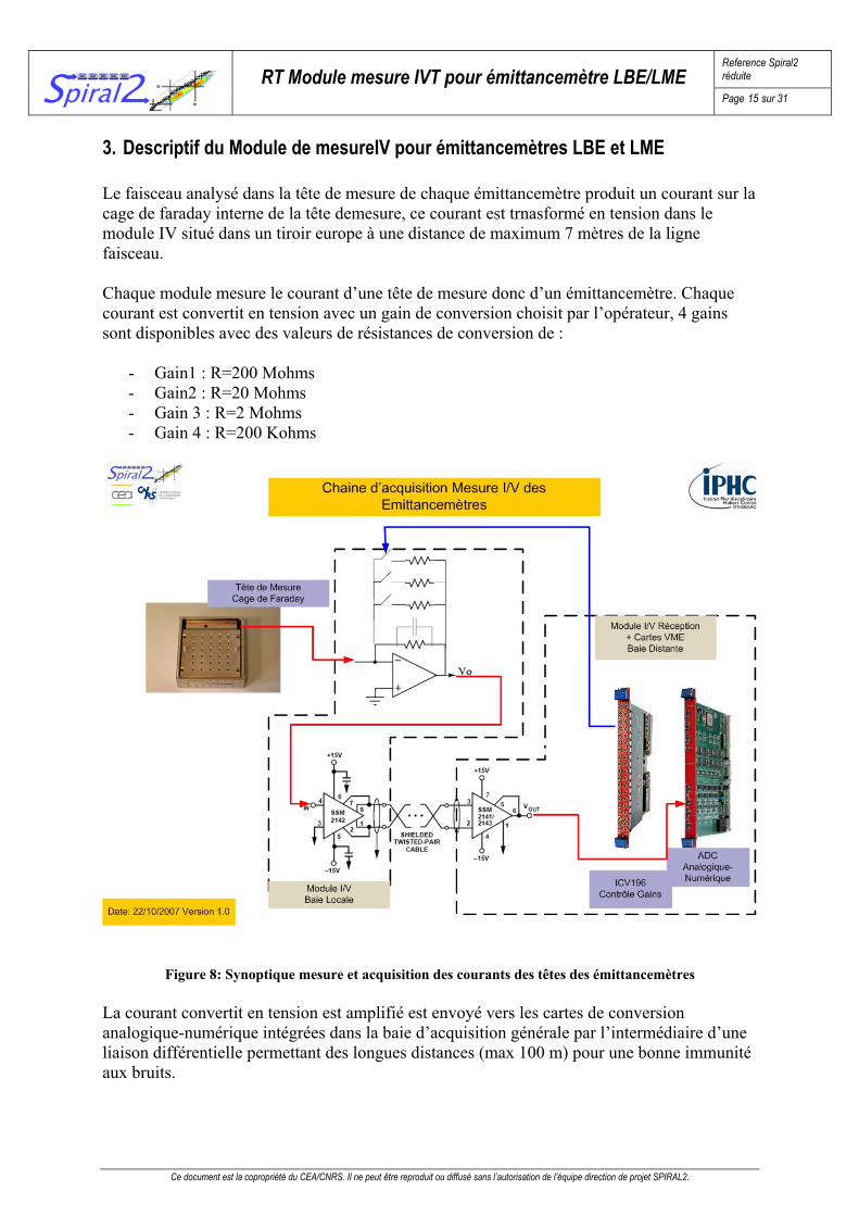
3. Descriptif du Module de mesureIV pour émittancemètres LBE et LME Le faisceau analysé dans la tête de mesure de chaque émittancemètre produit un courant sur la cage de faraday interne de la tête demesure, ce courant est trnasformé en tension dans le module IV situé dans un tiroir europe à une distance de maximum 7 mètres de la ligne faisceau. Chaque module mesure le courant d’une tête de mesure donc d’un émittancemètre. Chaque courant est convertit en tension avec un gain de conversion choisit par l’opérateur, 4 gains sont disponibles avec des valeurs de résistances de conversion de :
- Gain1 : R=200 Mohms - Gain2 : R=20 Mohms - Gain 3 : R=2 Mohms - Gain 4 : R=200 Kohms
Figure 8: Synoptique mesure et acquisition des courants des têtes des émittancemètres La courant convertit en tension est amplifié est envoyé vers les cartes de conversion analogique-numérique intégrées dans la baie d’acquisition générale par l’intermédiaire d’une liaison différentielle permettant des longues distances (max 100 m) pour une bonne immunité aux bruits.
Reference Spiral2 réduite
RT Module mesure IVT pour émittancemètre LBE/LME
Page 16 sur 31
Ce document est la copropriété du CEA/CNRS. Il ne peut être reproduit ou diffusé sans l’autorisation de l’équipe direction de projet SPIRAL2.
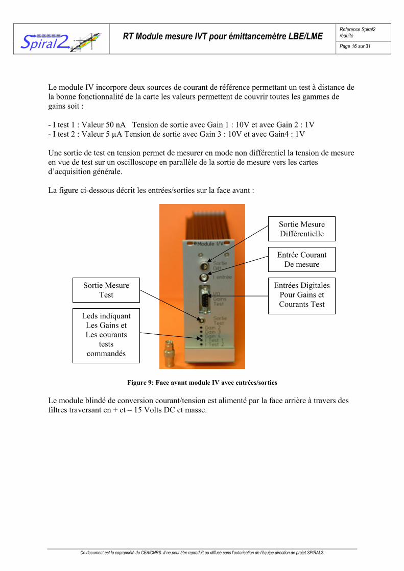
Le module IV incorpore deux sources de courant de référence permettant un test à distance de la bonne fonctionnalité de la carte les valeurs permettent de couvrir toutes les gammes de gains soit : - I test 1 : Valeur 50 nA Tension de sortie avec Gain 1 : 10V et avec Gain 2 : 1V - I test 2 : Valeur 5 µA Tension de sortie avec Gain 3 : 10V et avec Gain4 : 1V Une sortie de test en tension permet de mesurer en mode non différentiel la tension de mesure en vue de test sur un oscilloscope en parallèle de la sortie de mesure vers les cartes d’acquisition générale. La figure ci-dessous décrit les entrées/sorties sur la face avant :
Sortie Mesure Différentielle
Entrée Courant De mesure
Entrées Digitales Pour Gains et Courants Test
Sortie Mesure Test
Leds indiquant Les Gains et Les courants
tests commandés
Figure 9: Face avant module IV avec entrées/sorties
Le module blindé de conversion courant/tension est alimenté par la face arrière à travers des filtres traversant en + et – 15 Volts DC et masse.
Reference Spiral2 réduite
RT Module mesure IVT pour émittancemètre LBE/LME
Page 17 sur 31
Ce document est la copropriété du CEA/CNRS. Il ne peut être reproduit ou diffusé sans l’autorisation de l’équipe direction de projet SPIRAL2.
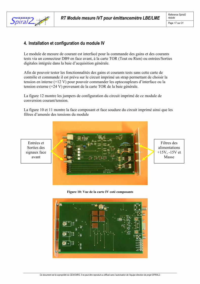
4. Installation et configuration du module IV Le module de mesure de courant est interfacé pour la commande des gains et des courants tests via un connecteur DB9 en face avant, à la carte TOR (Tout ou Rien) ou entrées/Sorties digitales intégrée dans la baie d’acquisition générale. Afin de pouvoir tester les fonctionnalités des gains et courants tests sans cette carte de contrôle et commande il est prévu sur le circuit imprimé un strap permettant de choisir la tension en interne (+12 V) pour pouvoir commander les optocoupleurs d’interface ou la tension externe (+24 V) provenant de la carte TOR de la baie générale. La figure 12 montre les jumpers de configuration du circuit imprimé de ce module de conversion courant/tension. La figure 10 et 11 montre la face composant et face soudure du circuit imprimé ainsi que les filtres d’amenée des tensions du module
Filtres des alimentations +15V, -15V et
Masse
Entrées et Sorties des
signaux face avant
Figure 10: Vue de la carte IV coté composants
Reference Spiral2 réduite
RT Module mesure IVT pour émittancemètre LBE/LME
Page 18 sur 31
Ce document est la copropriété du CEA/CNRS. Il ne peut être reproduit ou diffusé sans l’autorisation de l’équipe direction de projet SPIRAL2.
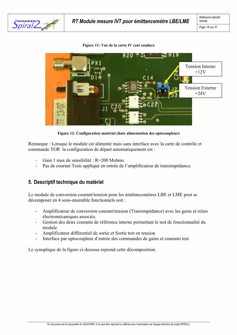
Figure 11: Vue de la carte IV coté soudure
Tension Interne +12V
Tension Externe +24V
Figure 12: Configuration matériel choix alimentation des optocoupleurs
Remarque : Lorsque le module est alimenté mais sans interface avec la carte de contrôle et commande TOR la configuration de départ automatiquement est :
- Gain 1 max de sensibilité : R=200 Mohms - Pas de courant Tests appliqué en entrée de l’amplificateur de transimpédance.
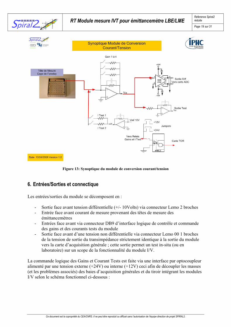
5. Descriptif technique du matériel Le module de conversion courant/tension pour les émittancemètres LBE et LME peut se décomposer en 4 sous-ensemble fonctionnels soit :
- Amplificateur de conversion courant/tension (Transimpédance) avec les gains et relais électromécaniques associés.
- Gestion des deux courants de référence interne permettant le test de fonctionnalité du module
- Amplificateur différentiel de sortie et Sortie test en tension - Interface par optocoupleur d’entrée des commandes de gains et courants test
Le synoptique de la figure ci-dessous reprend cette décomposition.
Reference Spiral2 réduite
RT Module mesure IVT pour émittancemètre LBE/LME
Page 19 sur 31
Ce document est la copropriété du CEA/CNRS. Il ne peut être reproduit ou diffusé sans l’autorisation de l’équipe direction de projet SPIRAL2.
Figure 13: Synoptique du module de conversion courant/tension
6. Entrées/Sorties et connectique Les entrées/sorties du module se décomposent en :
- Sortie face avant tension différentielle (+/- 10Volts) via connecteur Lemo 2 broches - Entrée face avant courant de mesure provenant des têtes de mesure des
émittancemètres - Entrées face avant via connecteur DB9 d’interface logique de contrôle et commande
des gains et des courants tests du module - Sortie face avant d’une tension non différentielle via connecteur Lemo 00 1 broches
de la tension de sortie du transimpédance strictement identique à la sortie du module vers la carte d’acquisition générale ; cette sortie permet un test in-situ (ou en laboratoire) sur un scope de la fonctionnalité du module I/V.
La commande logique des Gains et Courant Tests est faite via une interface par optocoupleur alimenté par une tension externe (+24V) ou interne (+12V) ceci afin de découpler les masses (et les problèmes associés) des baies d’acquisition générales et du tiroir intégrant les modules I/V selon le schéma fonctionnel ci-dessous :
Reference Spiral2 réduite
RT Module mesure IVT pour émittancemètre LBE/LME
Page 20 sur 31
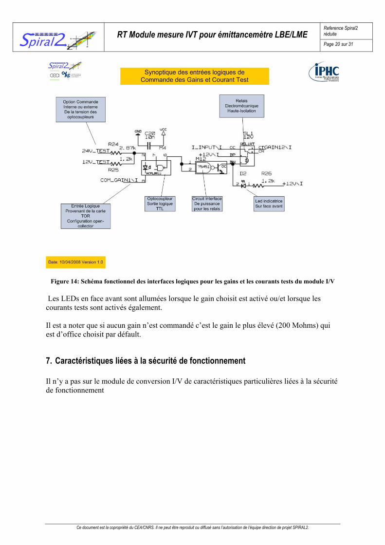
Ce document est la copropriété du CEA/CNRS. Il ne peut être reproduit ou diffusé sans l’autorisation de l’équipe direction de projet SPIRAL2.
Figure 14: Schéma fonctionnel des interfaces logiques pour les gains et les courants tests du module I/V Les LEDs en face avant sont allumées lorsque le gain choisit est activé ou/et lorsque les courants tests sont activés également. Il est a noter que si aucun gain n’est commandé c’est le gain le plus élevé (200 Mohms) qui est d’office choisit par défault.
7. Caractéristiques liées à la sécurité de fonctionnement Il n’y a pas sur le module de conversion I/V de caractéristiques particulières liées à la sécurité de fonctionnement
Reference Spiral2 réduite
RT Module mesure IVT pour émittancemètre LBE/LME
Page 21 sur 31
Ce document est la copropriété du CEA/CNRS. Il ne peut être reproduit ou diffusé sans l’autorisation de l’équipe direction de projet SPIRAL2.
8. Interfaces Mécaniques
Interfaces mécaniques
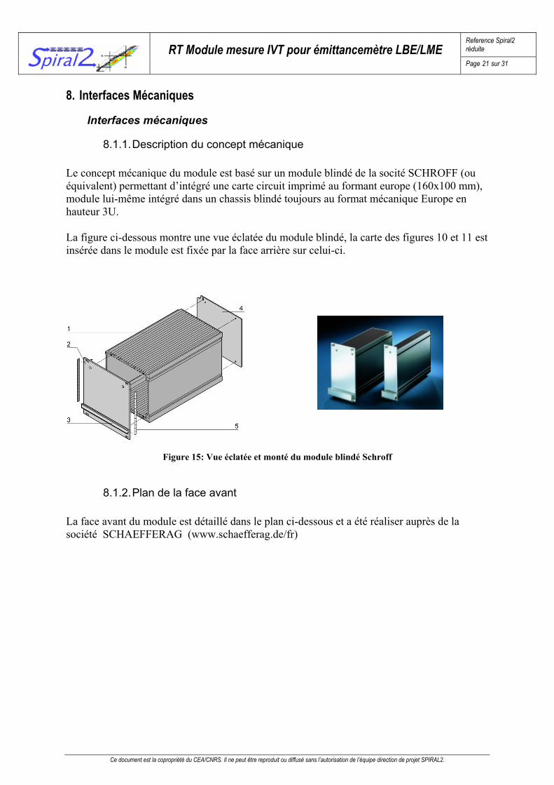
8.1.1. Description du concept mécanique Le concept mécanique du module est basé sur un module blindé de la socité SCHROFF (ou équivalent) permettant d’intégré une carte circuit imprimé au formant europe (160x100 mm), module lui-même intégré dans un chassis blindé toujours au format mécanique Europe en hauteur 3U. La figure ci-dessous montre une vue éclatée du module blindé, la carte des figures 10 et 11 est insérée dans le module est fixée par la face arrière sur celui-ci.
Figure 15: Vue éclatée et monté du module blindé Schroff
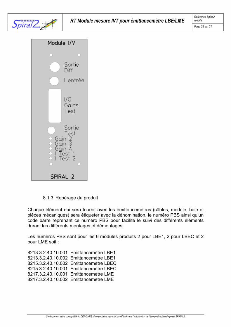
8.1.2. Plan de la face avant La face avant du module est détaillé dans le plan ci-dessous et a été réaliser auprès de la société SCHAEFFERAG (www.schaefferag.de/fr)
Reference Spiral2 réduite
RT Module mesure IVT pour émittancemètre LBE/LME
Page 22 sur 31
Ce document est la copropriété du CEA/CNRS. Il ne peut être reproduit ou diffusé sans l’autorisation de l’équipe direction de projet SPIRAL2.
8.1.3. Repérage du produit Chaque élément qui sera fournit avec les émittancemètres (câbles, module, baie et piêces mécaniques) sera étiqueter avec la dénomination, le numéro PBS ainsi qu’un code barre reprenant ce numéro PBS pour facilité le suivi des différents éléments durant les différents montages et démontages. Les numéros PBS sont pour les 6 modules produits 2 pour LBE1, 2 pour LBEC et 2 pour LME soit : 8213.3.2.40.10.001 Emittancemètre LBE1 8213.3.2.40.10.002 Emittancemètre LBE1 8215.3.2.40.10.002 Emittancemètre LBEC 8215.3.2.40.10.001 Emittancemètre LBEC 8217.3.2.40.10.001 Emittancemètre LME 8217.3.2.40.10.002 Emittancemètre LME

Reference Spiral2 réduite
RT Module mesure IVT pour émittancemètre LBE/LME
Page 23 sur 31
Ce document est la copropriété du CEA/CNRS. Il ne peut être reproduit ou diffusé sans l’autorisation de l’équipe direction de projet SPIRAL2.
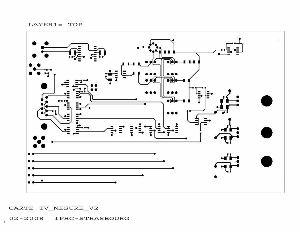
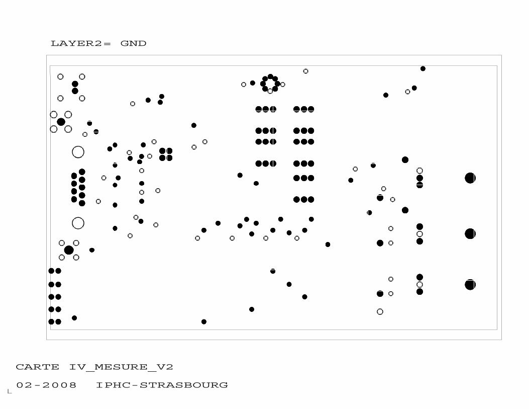
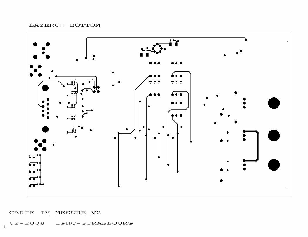
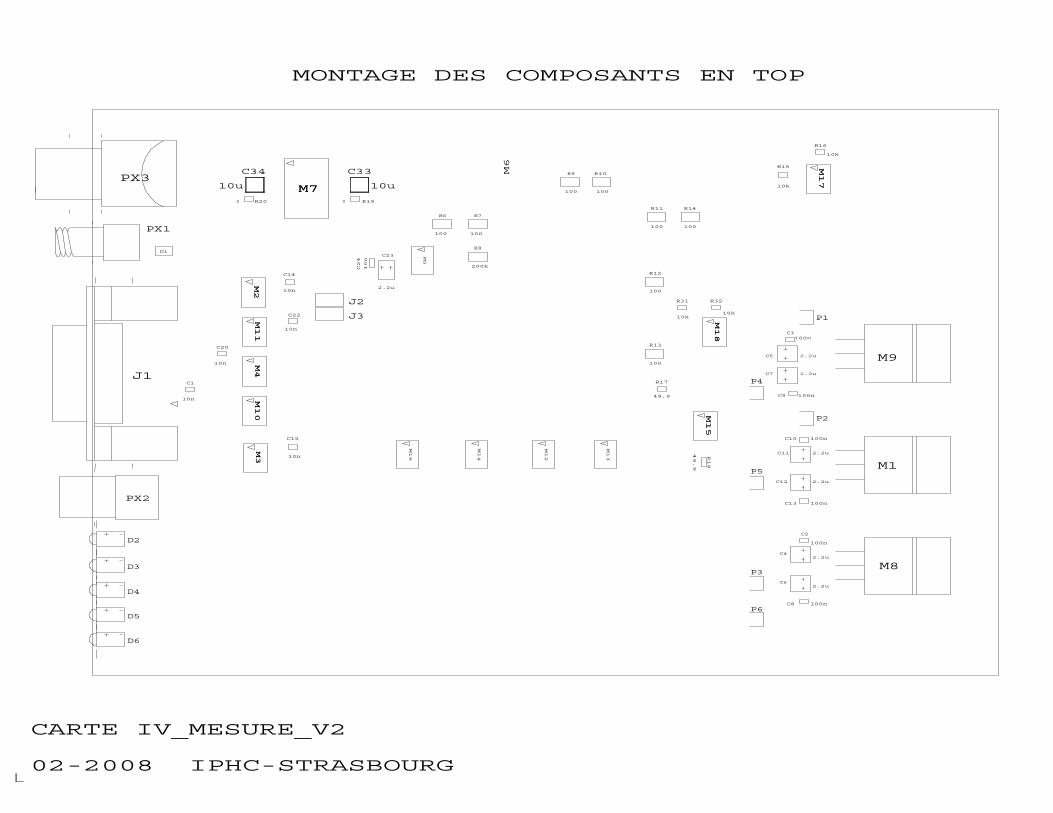
9. Dossier de Fabrication Ce chapitre décrit tous les fichiers utilisés pour la fabrication du module de conversion courant/tension pour les émittancemètres. Il comprend les nomenclatures des composants ; les vues des différentes couches du circuit imprimés principal et des photos du module monté sous différents angles.

Reference Spiral2 réduite
RT Module mesure IVT pour émittancemètre LBE/LME
Page 24 sur 31
Ce document est la copropriété du CEA/CNRS. Il ne peut être reproduit ou diffusé sans l’autorisation de l’équipe direction de projet SPIRAL2.
Nomenclatures Composants Cette nomenclature reprend les références fabricants, les références fournisseurs ainsi que les prix au 17/07/2008.
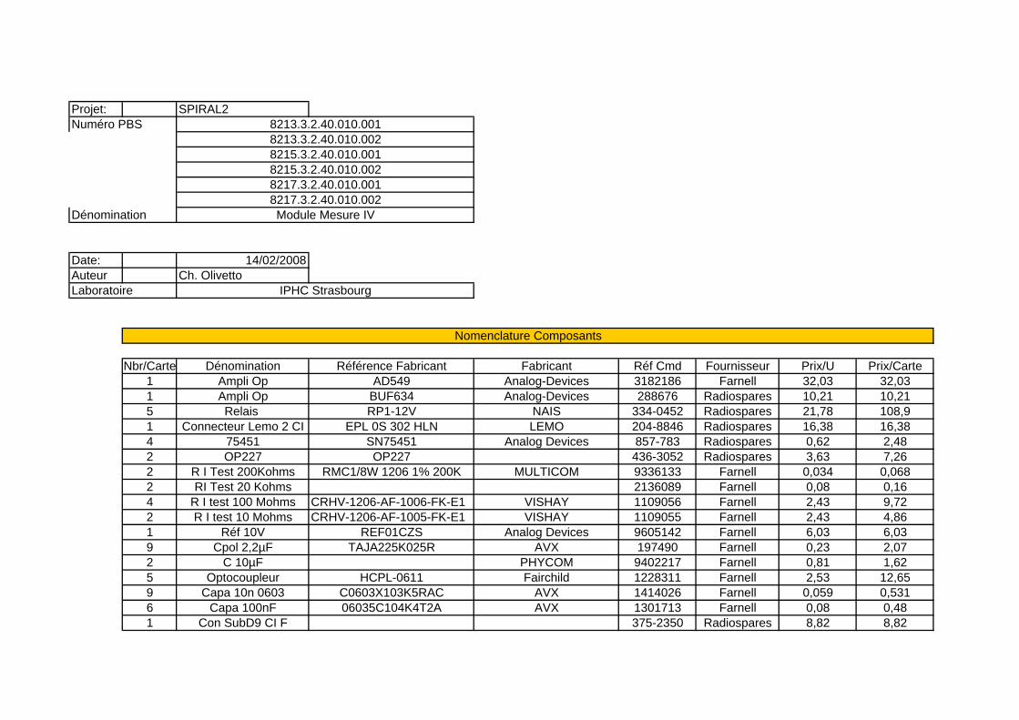
Projet: SPIRAL2Numéro PBS
Dénomination
Date: 14/02/2008Auteur Ch. OlivettoLaboratoire
Nbr/Carte Dénomination Référence Fabricant Fabricant Réf Cmd Fournisseur Prix/U Prix/Carte1 Ampli Op AD549 Analog-Devices 3182186 Farnell 32,03 32,031 Ampli Op BUF634 Analog-Devices 288676 Radiospares 10,21 10,215 Relais RP1-12V NAIS 334-0452 Radiospares 21,78 108,91 Connecteur Lemo 2 CI EPL 0S 302 HLN LEMO 204-8846 Radiospares 16,38 16,384 75451 SN75451 Analog Devices 857-783 Radiospares 0,62 2,482 OP227 OP227 436-3052 Radiospares 3,63 7,262 R I Test 200Kohms RMC1/8W 1206 1% 200K MULTICOM 9336133 Farnell 0,034 0,0682 RI Test 20 Kohms 2136089 Farnell 0,08 0,164 R I test 100 Mohms CRHV-1206-AF-1006-FK-E1 VISHAY 1109056 Farnell 2,43 9,722 R I test 10 Mohms CRHV-1206-AF-1005-FK-E1 VISHAY 1109055 Farnell 2,43 4,861 Réf 10V REF01CZS Analog Devices 9605142 Farnell 6,03 6,039 Cpol 2,2µF TAJA225K025R AVX 197490 Farnell 0,23 2,072 C 10µF PHYCOM 9402217 Farnell 0,81 1,625 Optocoupleur HCPL-0611 Fairchild 1228311 Farnell 2,53 12,659 Capa 10n 0603 C0603X103K5RAC AVX 1414026 Farnell 0,059 0,5316 Capa 100nF 06035C104K4T2A AVX 1301713 Farnell 0,08 0,481 Con SubD9 CI F 375-2350 Radiospares 8,82 8,82
Nomenclature Composants
8217.3.2.40.010.0018217.3.2.40.010.002Module Mesure IV
IPHC Strasbourg
8213.3.2.40.010.0018213.3.2.40.010.0028215.3.2.40.010.0018215.3.2.40.010.002
1 Con Lemo 50 ohms CI EPL.00.250.NTN Lemo 3817866 Farnell 8,99 8,991 Driver Diff SSM2142SZ Analog-Devices 9426329 Farnell 4,68 4,681 Régulateur +5V KA78T05 FAICHILD 1014074 Farnell 2,46 2,461 Régulateur +12V MC7812CTG ON SEMICONDUCTOR 9666109 Farnell 0,73 0,731 Régulateur -12V MC7912CT ON SEMICONDUCTOR 701920 Farnell 0,55 0,553 Radiateurs TO220 FK 224 MI 220-1 FISCHER ELEKTRONIK 4621128 Farnell 0,74 2,221 Module Europe 10F Schroff 442-1445 Radiospares 38,7 38,71 Con SMA coudé 112-4107 Radiospares 8,27 8,273 Filtre Alims FA FLMP5000 OXLEY 239-208 Radiospares 17,08 51,241 Diodes BAV199 BAV-199 Siemens 436-7830 Radiospares 3,6 3,65 Led coudée 228-5001 Radiospares 0,74 3,72 Barette SIL 173-3026 Radiospares 11,72 23,442 R=0 ohms 603 010 R=1,2 K 603 05 R=2,87 K 603 04 R=10 K 603 02 R=49,9 603 01 Circuit Imprimé IV_MESURE SCPI SCPI 147,18 147,181 Face Avant Sérigraphie SCHAEFFER SCHAEFFER 24,1 24,1
Total 247,612 544,129
2 Fiche Lemo 2 FA FFA0S302CLAC37 LEMO 173-2001 Radiospares 14,33 28,661 Cable Paire Torsadée 8451 010U500 BELDEN 1182101 Farnell 155,95 155,95
728,739Total avec cable mesure
Liste du Materiel pour Magasin
Notes Reference Valeur Type Taille Divers1
Condensateurs CMS6 CAPA 10n C603S50V10% CCNNI CMS 0603 Entre-Axes 1.60mm MURATA/GRM39X7R103K3 CAPA 10n SX7R50V Capa cerma X7R 50V en 06032 CAPA 10u 1210-16V CMS Format 12106 CAPA 100n C603S25V5% CMS 0603 Entre-Axes 1.60mm9 CPOL 2.2u T35X28S20V CMS TANTAL 10% Entre-Axes 3.5mm VISHAY/293D225X
Diodes5 LED2MMR_C ROUGE2MMC LED 2mm coudee rouge moulee dans un boitier 2.54mmX5
Diodes CMS1 BAV99 SOT CMS boitier SOT23
Connecteurs2 CON2P BAR-SILWRA pee a 2P Barrette droite (SIL) male secable de 40 pins en ligne A W1 CONSUBD9P_CF SUBD COUD-F Connecteur SUB-D coude femelle 9 pins
Circuits Integres1 7805_H TO220H 7805 +5V TO220 Montage horizontal1 7812_H TO220H 7812 +12V TO220 Montage horizontal1 7912_H TO220H 7912 -12V TO220 Montage horizontal1 AD549_TO99 TO99 AD549J AD549JHZ ibias= 150pA Boitier TO99
Circuits Integres CMS1 BUF634_SOIC SOIC BB/BUF634U Boitier CMS 8 pattes5 HCPL0611_SOIC SOIC AGIL/HCPL-0611 Plastic CMS 8 pins2 OPA227 SOIC OPA227UA Plastic CMS 8 pins1 REF01 SOIC Small Outline Z_leaded 8 pins 6.00mm4 SN75451BD SOIC SN75451BD SOP 8 pins en Z Corps_3.9mm Pas_1.27mm1 SSM2142_SOIC SOIC AD/SSM2142S Boitier CMS large 16 pattes
Pastilles, Points de test et Prises6 PASCON PASTILLE183 Pastille de connection diametre 1.83mm trou 1.1mm
Resistances CMS2 RGEN 0 0603-1% CMS 0603 1%
NBR Cartes
Genere avec vliste v15.51 3 / 6Carte IV_MESURE_V2
olivetto 13-Feb-2008 AT 16:35:43
Liste du Materiel pour Magasin
Notes Reference Valeur Type Taille Divers1
NBR Cartes
10 RGEN 1.2k S63MW5% CMS 0603 63mW 5%5 RGEN 2.87k S63MW1% CMS 0603 63mW 1%4 RGEN 10k S63MW5% SERE CMS 0603 63mW 5%2 RGEN 49.9 S63MW1% CMS 0603 63mW 1%8 RGEN 100 S250MW1% RMAYH CMS 1206 250mW 1%1 RGEN 200k S250MW1% CMS 1206 250mW 1%
Relais5 REL1RT 12V RP NAIS/RP1H12 Relais HF Low Profile 1RT 12V 1028 ohms
Divers1 PCOAX PRISE-SMA_C Embase coudee serie SMA1 PCOAX PRISE-LEMO_C KCCFC Embase coudee LEMO/EPL00250DTN1 PLEMO2SIGN PLEMO2 Embase lemo BIFILAIRE SERIE S LEMO/EPL0S302HLN
Genere avec vliste v15.51 4 / 6Carte IV_MESURE_V2
olivetto 13-Feb-2008 AT 16:35:43
Liste du Materiel pour Montage
Notes Reference Valeur Type Taille Divers
Condensateurs CMSCAPA 10n C603S50V10% CCNNI CMS 0603 Entre-Axes 1.60mm MURATA/GRM39X7R103K C1 C14 C15 C20 C21
C22CAPA 10n SX7R50V Capa cerma X7R 50V en 0603 C24 C27 C31CAPA 10u 1210-16V CMS Format 1210 C33 C34CAPA 100n C603S25V5% CMS 0603 Entre-Axes 1.60mm C2 C3 C8 C9 C10
C13CPOL 2.2u T35X28S20V CMS TANTAL 10% Entre-Axes 3.5mm VISHAY/293D225X C4 C5 C6 C7 C11
C12 C23 C25 C29
DiodesLED2MMR_C ROUGE2MMC LED 2mm coudee rouge moulee dans un boitier 2.54mmX5 D2 D3 D4 D5 D6
Diodes CMSBAV99 SOT CMS boitier SOT23 D1
ConnecteursCON2P BAR-SILWRA pee a 2P Barrette droite (SIL) male secable de 40 pins en ligne A W J2 J3CONSUBD9P_CF SUBD COUD-F Connecteur SUB-D coude femelle 9 pins J1
Circuits Integres7805_H TO220H 7805 +5V TO220 Montage horizontal M17812_H TO220H 7812 +12V TO220 Montage horizontal M87912_H TO220H 7912 -12V TO220 Montage horizontal M9AD549_TO99 TO99 AD549J AD549JHZ ibias= 150pA Boitier TO99 M6
Circuits Integres CMSBUF634_SOIC SOIC BB/BUF634U Boitier CMS 8 pattes M15HCPL0611_SOIC SOIC AGIL/HCPL-0611 Plastic CMS 8 pins M2 M3 M4 M10 M11OPA227 SOIC OPA227UA Plastic CMS 8 pins M17 M18REF01 SOIC Small Outline Z_leaded 8 pins 6.00mm M5SN75451BD SOIC SN75451BD SOP 8 pins en Z Corps_3.9mm Pas_1.27mm M12 M13 M14 M16SSM2142_SOIC SOIC AD/SSM2142S Boitier CMS large 16 pattes M7
Pastilles, Points de test et PrisesPASCON PASTILLE183 Pastille de connection diametre 1.83mm trou 1.1mm P1 P2 P3 P4 P5
P6
Resistances CMSRGEN 0 0603-1% CMS 0603 1% R19 R20RGEN 1.2k S63MW5% CMS 0603 63mW 5% R2 R4 R21 R23 R25
R26 R27 R28 R29 R30RGEN 2.87k S63MW1% CMS 0603 63mW 1% R1 R3 R5 R22 R24
Ref-Des
Genere avec vliste v15.51 5 / 6Carte IV_MESURE_V2
olivetto 13-Feb-2008 AT 16:35:43
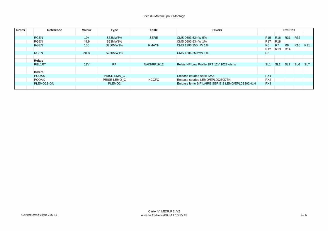
Liste du Materiel pour Montage
Notes Reference Valeur Type Taille Divers Ref-Des
RGEN 10k S63MW5% SERE CMS 0603 63mW 5% R15 R16 R31 R32RGEN 49.9 S63MW1% CMS 0603 63mW 1% R17 R18RGEN 100 S250MW1% RMAYH CMS 1206 250mW 1% R6 R7 R9 R10 R11
R12 R13 R14RGEN 200k S250MW1% CMS 1206 250mW 1% R8
RelaisREL1RT 12V RP NAIS/RP1H12 Relais HF Low Profile 1RT 12V 1028 ohms SL1 SL2 SL3 SL6 SL7
DiversPCOAX PRISE-SMA_C Embase coudee serie SMA PX1PCOAX PRISE-LEMO_C KCCFC Embase coudee LEMO/EPL00250DTN PX2PLEMO2SIGN PLEMO2 Embase lemo BIFILAIRE SERIE S LEMO/EPL0S302HLN PX3
Genere avec vliste v15.51 6 / 6Carte IV_MESURE_V2
olivetto 13-Feb-2008 AT 16:35:43

Reference Spiral2 réduite
RT Module mesure IVT pour émittancemètre LBE/LME
Page 25 sur 31
Ce document est la copropriété du CEA/CNRS. Il ne peut être reproduit ou diffusé sans l’autorisation de l’équipe direction de projet SPIRAL2.
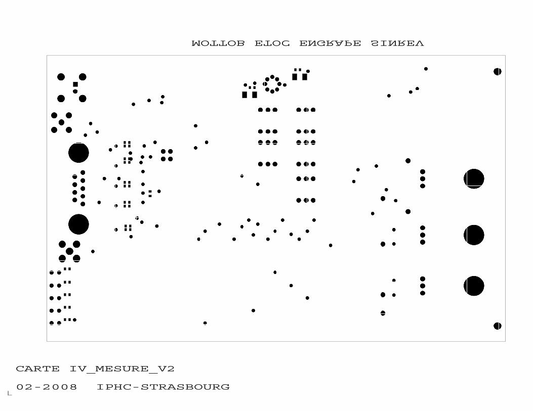
Circuit imprimé principal Nous retrouvons ici l’ensemble des vues des différentes couches du circuit imprimé ainsi que les vues du plan de perçage, de montage des composants et des sérigraphies.
CARTE IV_MESURE_V2
02-2008 IPHC-STRASBOURG
LAYER1= TOP
CARTE IV_MESURE_V2
02-2008 IPHC-STRASBOURG
LAYER2= GND
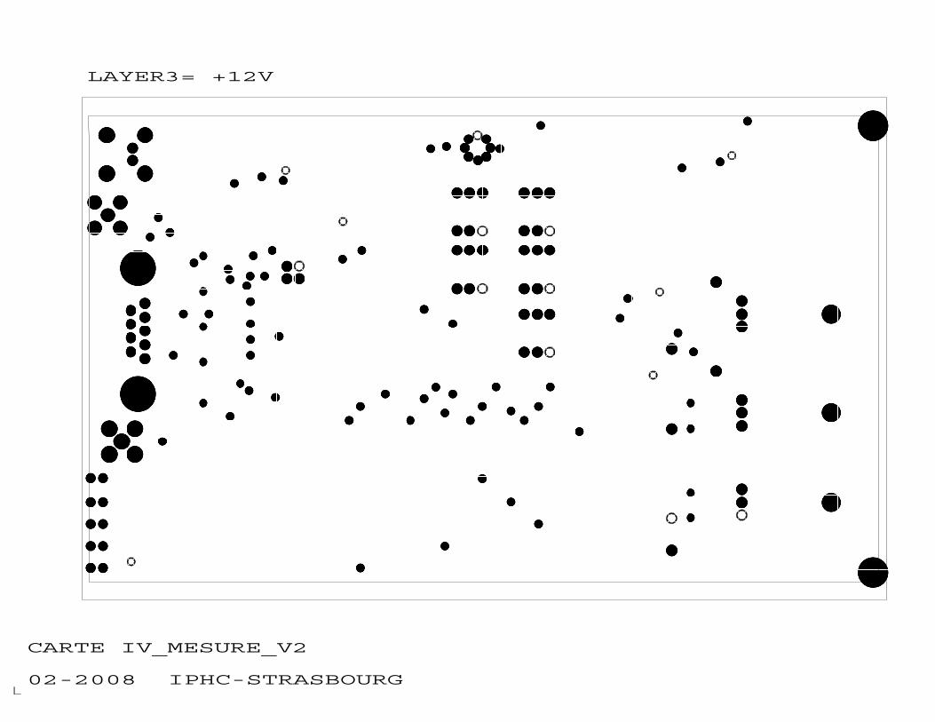
LAYER3= +12V
CARTE IV_MESURE_V2
02-2008 IPHC-STRASBOURG
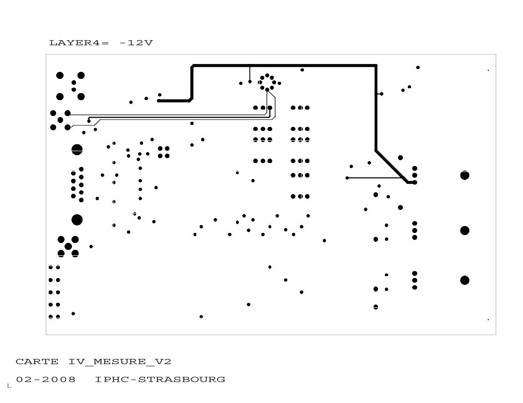
LAYER4= -12V
CARTE IV_MESURE_V2
02-2008 IPHC-STRASBOURG
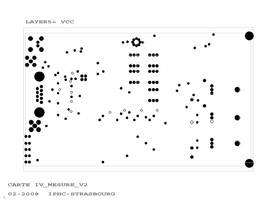
LAYER5= VCC
CARTE IV_MESURE_V2
02-2008 IPHC-STRASBOURG
CARTE IV_MESURE_V2
02-2008 IPHC-STRASBOURG
LAYER6= BOTTOM
R16
M17
C2
R15
C3
C5
C7
C10
C9
C11
C13
C12
C8
C4
C6
R14
R31 R32
M18
M15
R18
R10
R11
R12
R17
R13
M13
R9
M12
R7
R8
M14
R6
M5
C23
M16
M7R19
C24
R20
M2
C22
C14
M11
M4
M10
M3
C15
D1
C20
C1
M9
M1
M8
M17
P1
P2
P4
P5
P3
P6
M18
M15
M6
C33
M7
J2
J3
C34
M2
M11
M4
M10
M3
PX3
PX1
J1
PX2
D2
D3
D4
D5
D6
10k
100n
2.2u
100n
2.2u
100n
100n
2.2u
2.2u
10k
100n
2.2u
2.2u
100n
100
10k10k
49.9
100
100
100
100
49.9
100
100
200k
100
2.2u
0
10n
MONTAGE DES COMPOSANTS EN TOP
0
10n
10n
10n
10n
10n
10u10u
CARTE IV_MESURE_V2
02-2008 IPHC-STRASBOURG
C27
C25
10n
2.2u
10n
C31
2.2u
C29
C21
MONTAGE DES COMPOSANTS EN BOTTOM
R3
2.87k
R5
1.2k
R21
10n
1.2k
R42.87k
R24
1.2k
R25
2.87k
R1
1.2k
R2
2.87k
R22
1.2k
R23
2.87k
1.2k
R26
1.2k
R27
1.2k
R28
R29
1.2k
1.2k
R30
CARTE IV_MESURE_V2
02-2008 IPHC-STRASBOURG
SERIGRAPHIE COTE TOP
CARTE IV_MESURE_V2
02-2008 IPHC-STRASBOURG
M9
M1
M8
R16
M17
SPIRAL2
EMITTANCEMETRE
CARTE IV_MESURE
C5
C7
C10
C9
P2
C12
C6
R15
P1
C3
P4
C11
C2
C13
P5
C4
P3
C8P6
R14
R31 R32
M18
M15
R18
R10R11
R12
R17
R13
M13
VERSION:2.0
R9
M12
DATE:07/02/2008
M6
R7
R8
M14
C33
C23
R6
M5
M16
M7
R19
C24
J2
J3
C34
R20
M2
C14
M11
M4
C22
M10
M3
C15
PX3
J1C20
C1
PX2
PX1
D1
D2
D3
D4
D5
D6
SERIGRAPHIE COTE BOTTOM
CARTE IV_MESURE_V2
02-2008 IPHC-STRASBOURG
M9M1
M8
P1
P4
P2
P5P3
P6
C27
C25SL1
SL2
SL3
SL7
SL6
M6
C31
C29
J2J3
R3
R21
C21
R1R2
R5
J1
R4R24
R25
R23
PX2
R22
PX3
PX1
D2
R26
R27
R28
D3D4
D5
R29
R30
D6
VERNIS EPARGNE COTE TOP
CARTE IV_MESURE_V2
02-2008 IPHC-STRASBOURG
VERNIS EPARGNE COTE BOTTOM
CARTE IV_MESURE_V2
02-2008 IPHC-STRASBOURG
Reference Spiral2 réduite
RT Module mesure IVT pour émittancemètre LBE/LME
Page 26 sur 31
Ce document est la copropriété du CEA/CNRS. Il ne peut être reproduit ou diffusé sans l’autorisation de l’équipe direction de projet SPIRAL2.
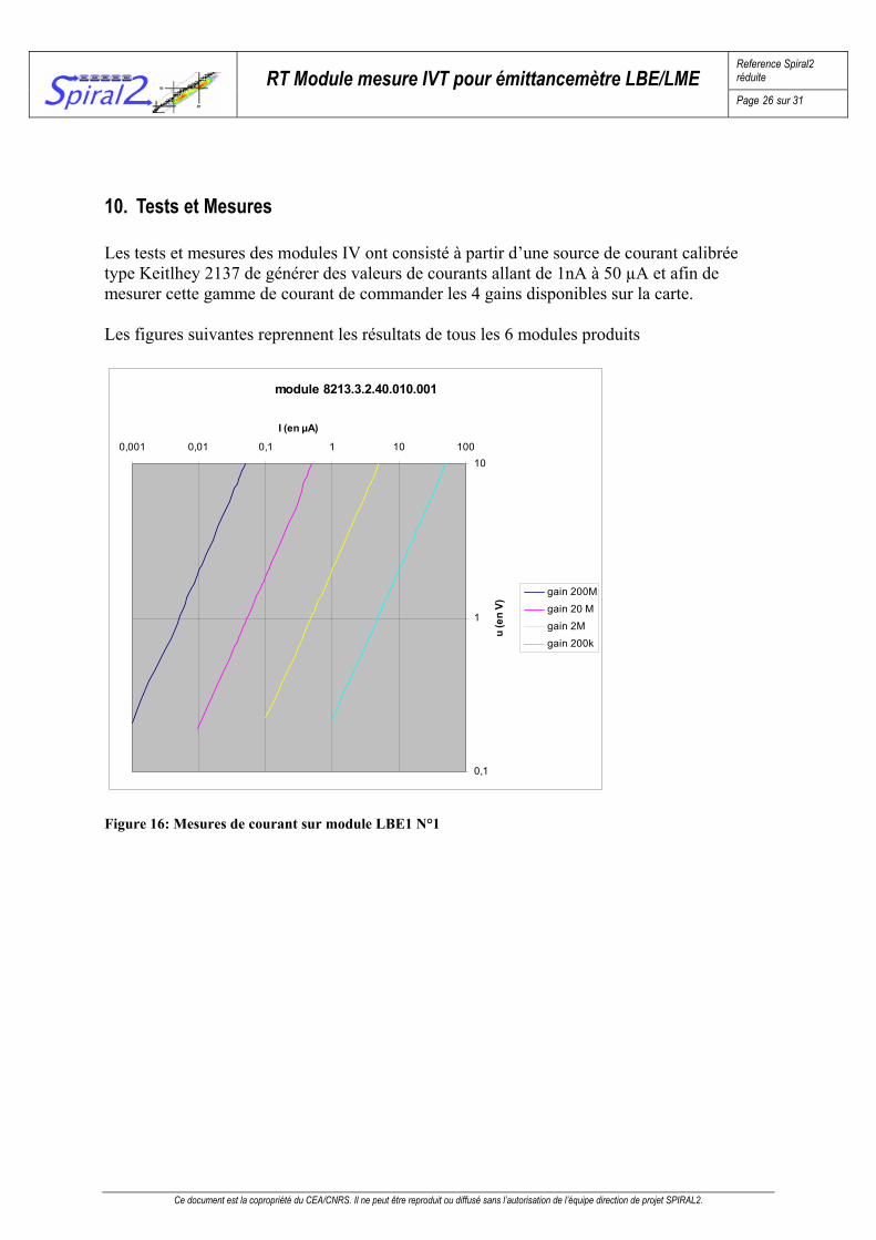
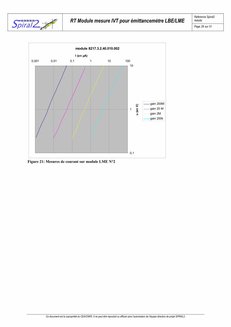
10. Tests et Mesures Les tests et mesures des modules IV ont consisté à partir d’une source de courant calibrée type Keitlhey 2137 de générer des valeurs de courants allant de 1nA à 50 µA et afin de mesurer cette gamme de courant de commander les 4 gains disponibles sur la carte. Les figures suivantes reprennent les résultats de tous les 6 modules produits
module 8213.3.2.40.010.001
0,1
1
100,001 0,01 0,1 1 10 100
I (en µA)
u (e
n V)
gain 200M
gain 20 M
gain 2M
gain 200k
Figure 16: Mesures de courant sur module LBE1 N°1
Reference Spiral2 réduite
RT Module mesure IVT pour émittancemètre LBE/LME
Page 27 sur 31
Ce document est la copropriété du CEA/CNRS. Il ne peut être reproduit ou diffusé sans l’autorisation de l’équipe direction de projet SPIRAL2.
module 8213.3.2.40.010.002
0,1
1
100,0001 0,001 0,01 0,1 1 10 100
I (en µA)
u (e
n V)
gain 200Mgain 20 Mgain 2Mgain 200k
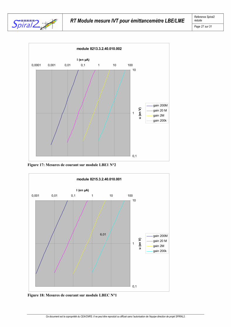
Figure 17: Mesures de courant sur module LBE1 N°2
module 8215.3.2.40.010.001
0,1
1
100,001 0,01 0,1 1 10 100
I (en µA)
u (e
n V)
gain 200Mgain 20 Mgain 2Mgain 200k
6,01
Figure 18: Mesures de courant sur module LBEC N°1
Reference Spiral2 réduite
RT Module mesure IVT pour émittancemètre LBE/LME
Page 28 sur 31
Ce document est la copropriété du CEA/CNRS. Il ne peut être reproduit ou diffusé sans l’autorisation de l’équipe direction de projet SPIRAL2.
module 8215.3.2.40.010.002
0,1
1
100,001 0,01 0,1 1 10 100
I (en µA)
u (e
n V)
gain 200Mgain 20 Mgain 2Mgain 200k
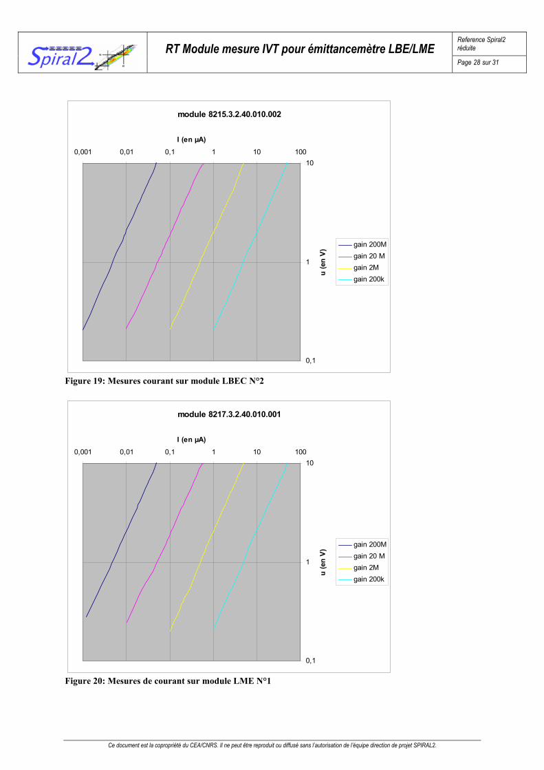
Figure 19: Mesures courant sur module LBEC N°2
module 8217.3.2.40.010.001
0,1
1
100,001 0,01 0,1 1 10 100
I (en µA)
u (e
n V)
gain 200Mgain 20 Mgain 2Mgain 200k
Figure 20: Mesures de courant sur module LME N°1
Reference Spiral2 réduite
RT Module mesure IVT pour émittancemètre LBE/LME
Page 29 sur 31
Ce document est la copropriété du CEA/CNRS. Il ne peut être reproduit ou diffusé sans l’autorisation de l’équipe direction de projet SPIRAL2.
module 8217.3.2.40.010.002
0,1
1
100,001 0,01 0,1 1 10 100
I (en µA)
u (e
n V)
gain 200Mgain 20 Mgain 2Mgain 200k
Figure 21: Mesures de courant sur module LME N°2

Reference Spiral2 réduite
RT Module mesure IVT pour émittancemètre LBE/LME
Page 30 sur 31
Ce document est la copropriété du CEA/CNRS. Il ne peut être reproduit ou diffusé sans l’autorisation de l’équipe direction de projet SPIRAL2.

Reference Spiral2 réduite
RT Module mesure IVT pour émittancemètre LBE/LME
Page 31 sur 31
Ce document est la copropriété du CEA/CNRS. Il ne peut être reproduit ou diffusé sans l’autorisation de l’équipe direction de projet SPIRAL2.
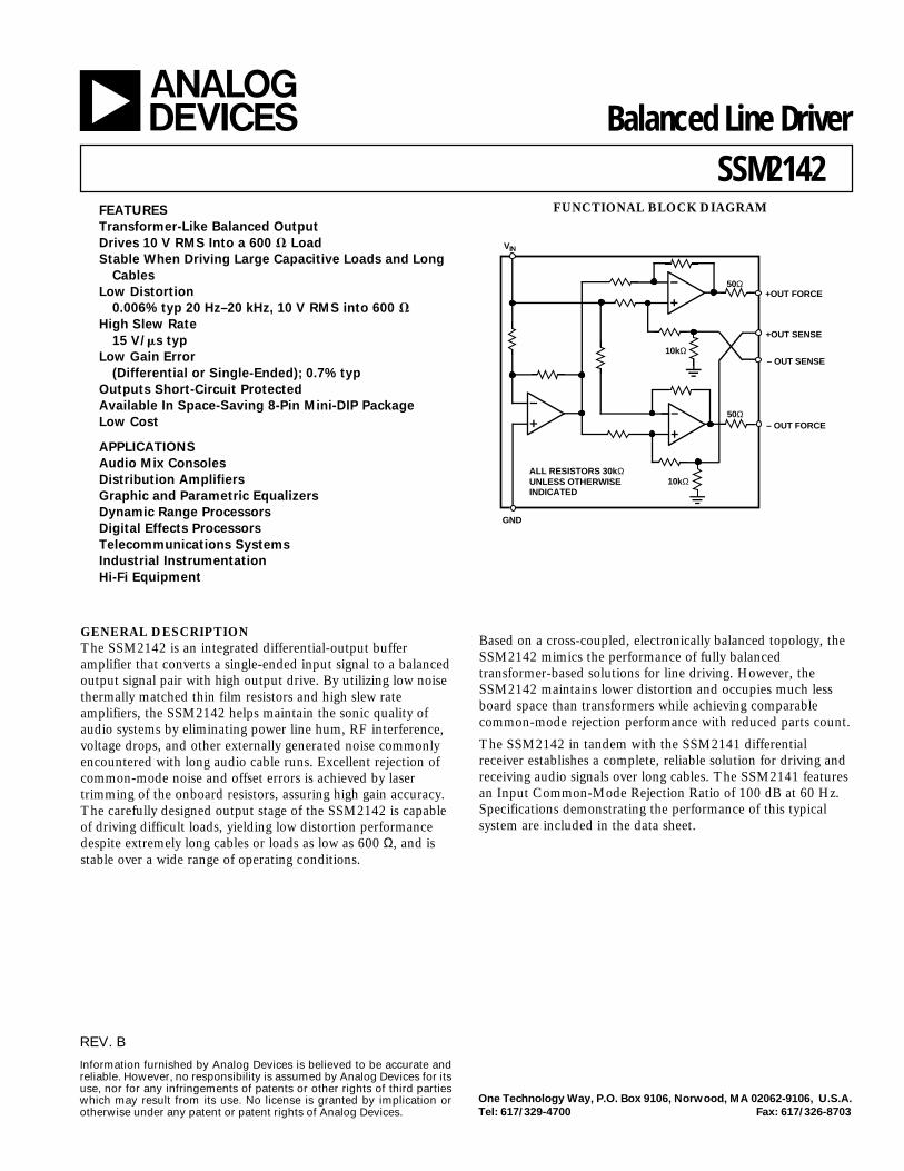
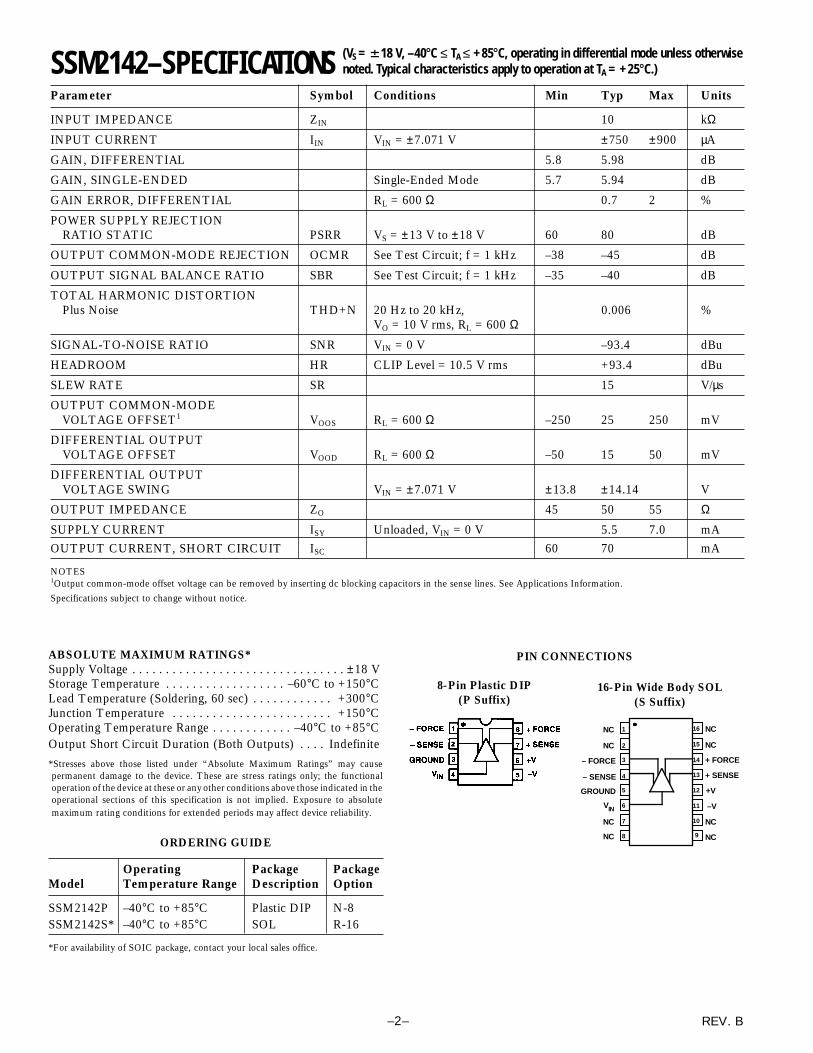
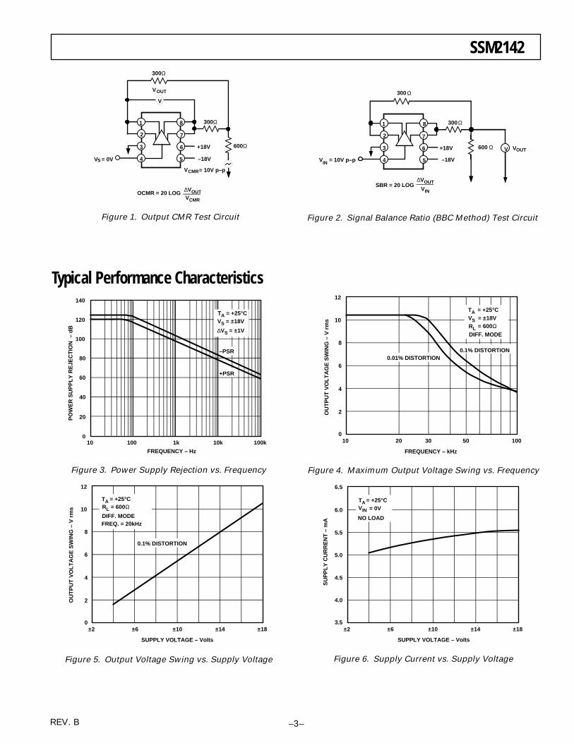
Annexes : Datasheet principaux composants Dans les pages suivantes vous trouverez les datasheets des principaux composants utilisés dans le module de conversion IV pour les émittancemètres des lignes LBE et LME :
FUNCTIONAL BLOCK DIAGRAM
+OUT FORCE
– OUT FORCE
– OUT SENSE
+OUT SENSE
10kΩ
10kΩ
50Ω
50Ω
VIN
GND
ALL RESISTORS 30kΩ UNLESS OTHERWISE INDICATED
REV. B
Information furnished by Analog Devices is believed to be accurate andreliable. However, no responsibility is assumed by Analog Devices for itsuse, nor for any infringements of patents or other rights of third partieswhich may result from its use. No license is granted by implication orotherwise under any patent or patent rights of Analog Devices.
a Balanced Line DriverSSM2142
One Technology Way, P.O. Box 9106, Norwood, MA 02062-9106, U.S.A.
Tel: 617/329-4700 Fax: 617/326-8703
FEATURES
Transformer-Like Balanced Output
Drives 10 V RMS Into a 600 V Load
Stable When Driving Large Capacitive Loads and Long
Cables
Low Distortion
0.006% typ 20 Hz–20 kHz, 10 V RMS into 600 VHigh Slew Rate
15 V/ms typ
Low Gain Error
(Differential or Single-Ended); 0.7% typ
Outputs Short-Circuit Protected
Available In Space-Saving 8-Pin Mini-DIP Package
Low Cost
APPLICATIONS
Audio Mix Consoles
Distribution Amplifiers
Graphic and Parametric Equalizers
Dynamic Range Processors
Digital Effects Processors
Telecommunications Systems
Industrial Instrumentation
Hi-Fi Equipment
GENERAL DESCRIPTIONThe SSM2142 is an integrated differential-output bufferamplifier that converts a single-ended input signal to a balancedoutput signal pair with high output drive. By utilizing low noisethermally matched thin film resistors and high slew rateamplifiers, the SSM2142 helps maintain the sonic quality ofaudio systems by eliminating power line hum, RF interference,voltage drops, and other externally generated noise commonlyencountered with long audio cable runs. Excellent rejection ofcommon-mode noise and offset errors is achieved by lasertrimming of the onboard resistors, assuring high gain accuracy.The carefully designed output stage of the SSM2142 is capableof driving difficult loads, yielding low distortion performancedespite extremely long cables or loads as low as 600 Ω, and isstable over a wide range of operating conditions.
Based on a cross-coupled, electronically balanced topology, theSSM2142 mimics the performance of fully balancedtransformer-based solutions for line driving. However, theSSM2142 maintains lower distortion and occupies much lessboard space than transformers while achieving comparablecommon-mode rejection performance with reduced parts count.
The SSM2142 in tandem with the SSM2141 differentialreceiver establishes a complete, reliable solution for driving andreceiving audio signals over long cables. The SSM2141 featuresan Input Common-Mode Rejection Ratio of 100 dB at 60 Hz.Specifications demonstrating the performance of this typicalsystem are included in the data sheet.
REV. B
SSM2142–SPECIFICATIONSParameter Symbol Conditions Min Typ Max Units
INPUT IMPEDANCE ZIN 10 kΩINPUT CURRENT IIN VIN = ±7.071 V ±750 ±900 µA
GAIN, DIFFERENTIAL 5.8 5.98 dB
GAIN, SINGLE-ENDED Single-Ended Mode 5.7 5.94 dB
GAIN ERROR, DIFFERENTIAL RL = 600 Ω 0.7 2 %
POWER SUPPLY REJECTIONRATIO STATIC PSRR VS = ±13 V to ±18 V 60 80 dB
OUTPUT COMMON-MODE REJECTION OCMR See Test Circuit; f = 1 kHz –38 –45 dB
OUTPUT SIGNAL BALANCE RATIO SBR See Test Circuit; f = 1 kHz –35 –40 dB
TOTAL HARMONIC DISTORTIONPlus Noise THD+N 20 Hz to 20 kHz, 0.006 %
VO = 10 V rms, RL = 600 ΩSIGNAL-TO-NOISE RATIO SNR VIN = 0 V –93.4 dBu
HEADROOM HR CLIP Level = 10.5 V rms +93.4 dBu
SLEW RATE SR 15 V/µs
OUTPUT COMMON-MODEVOLTAGE OFFSET1 VOOS RL = 600 Ω –250 25 250 mV
DIFFERENTIAL OUTPUTVOLTAGE OFFSET VOOD RL = 600 Ω –50 15 50 mV
DIFFERENTIAL OUTPUTVOLTAGE SWING VIN = ±7.071 V ±13.8 ±14.14 V
OUTPUT IMPEDANCE ZO 45 50 55 ΩSUPPLY CURRENT ISY Unloaded, VIN = 0 V 5.5 7.0 mA
OUTPUT CURRENT, SHORT CIRCUIT ISC 60 70 mA
NOTES1Output common-mode offset voltage can be removed by inserting dc blocking capacitors in the sense lines. See Applications Information.
Specifications subject to change without notice.
(VS = 618 V, –408C ≤ TA ≤ +858C, operating in differential mode unless otherwisenoted. Typical characteristics apply to operation at TA = +258C.)
ABSOLUTE MAXIMUM RATINGS*Supply Voltage . . . . . . . . . . . . . . . . . . . . . . . . . . . . . . . . ±18 VStorage Temperature . . . . . . . . . . . . . . . . . . –60°C to +150°CLead Temperature (Soldering, 60 sec) . . . . . . . . . . . . +300°CJunction Temperature . . . . . . . . . . . . . . . . . . . . . . . . +150°COperating Temperature Range . . . . . . . . . . . . –40°C to +85°COutput Short Circuit Duration (Both Outputs) . . . . Indefinite
*Stresses above those listed under “Absolute Maximum Ratings” may causepermanent damage to the device. These are stress ratings only; the functionaloperation of the device at these or any other conditions above those indicated in theoperational sections of this specification is not implied. Exposure to absolutemaximum rating conditions for extended periods may affect device reliability.
ORDERING GUIDE
Operating Package PackageModel Temperature Range Description Option
SSM2142P –40°C to +85°C Plastic DIP N-8SSM2142S* –40°C to +85°C SOL R-16
*For availability of SOIC package, contact your local sales office.
PIN CONNECTIONS
8-Pin Plastic DIP(P Suffix)
–2–
16-Pin Wide Body SOL(S Suffix)
– FORCE
– SENSE
GROUND
VIN
+ FORCE
+ SENSE
+V
–V
NC
NC
NC
NC
NC
NC
NC
NC1
2
3
4
5
6
7
8
16
15
14
13
12
11
10
9
SSM2142
REV. B –3–
Typical Performance Characteristics
10
140
FREQUENCY – Hz
120
100
80
60
40
20
0100 1k 10k 100k
PO
WE
R S
UP
PL
Y R
EJE
CT
ION
– d
B
TA = +25°CVS = ±18V
∆VS = ±1V
–PSR
+PSR
Figure 3. Power Supply Rejection vs. Frequency
±2
SUPPLY VOLTAGE – Volts
12
10
8
6
4
2
0
OU
TP
UT
VO
LT
AG
E S
WIN
G –
V r
ms
0.1% DISTORTION
±6 ±10 ±14 ±18
TA = +25°C RL = 600ΩDIFF. MODEFREQ. = 20kHz
Figure 5. Output Voltage Swing vs. Supply Voltage
10
12
FREQUENCY – kHz
10
8
6
4
2
020 30 50 100
OU
TP
UT
VO
LT
AG
E S
WIN
G –
V r
ms
TA = +25°CVS = ±18VRL = 600ΩDIFF. MODE
0.1% DISTORTION0.01% DISTORTION
Figure 4. Maximum Output Voltage Swing vs. Frequency
±2
SUPPLY VOLTAGE – Volts
6.5
SU
PP
LY
CU
RR
EN
T –
mA
±6 ±10 ±14 ±18
TA = +25°CVIN = 0V
NO LOAD6.0
5.5
5.0
4.5
4.0
3.5
Figure 6. Supply Current vs. Supply Voltage
2
VOUT
V
300Ω
300Ω
600Ω+18V
–18VVS = 0V
VCMR= 10V p–p
∆VOUTVCMR
OCMR = 20 LOG
1
3
4 5
6
7
8
Figure 1. Output CMR Test Circuit
300
300
600+18V
–18VV = 10V p–pIN
∆VOUT
VINSBR = 20 LOG
VOUT
2
1
3
4 5
6
7
8
V
Ω
Ω
Ω
Figure 2. Signal Balance Ratio (BBC Method) Test Circuit
SSM2142
–4– REV. B
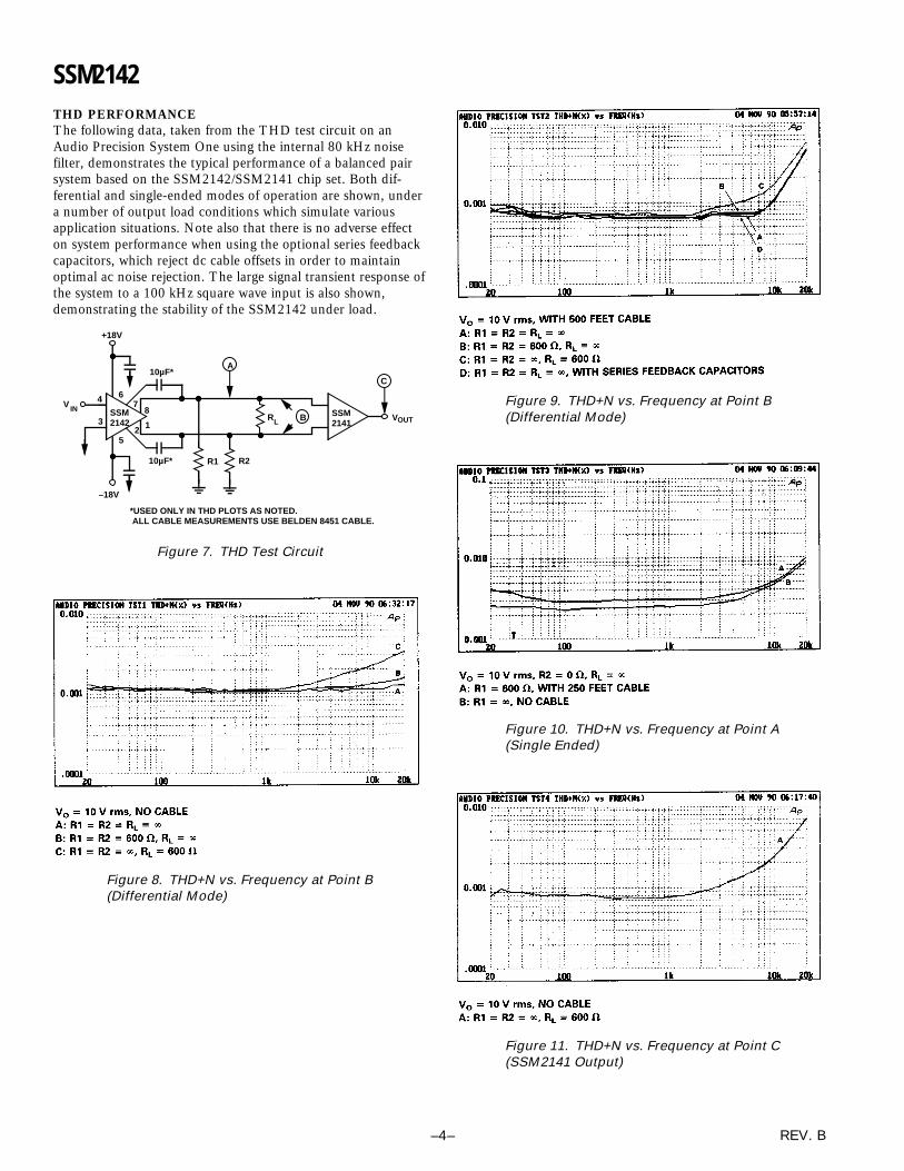
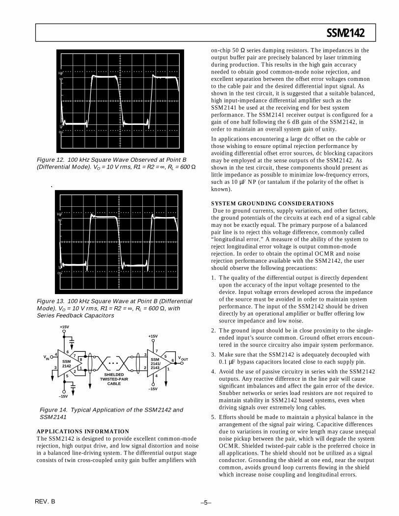
THD PERFORMANCEThe following data, taken from the THD test circuit on anAudio Precision System One using the internal 80 kHz noisefilter, demonstrates the typical performance of a balanced pairsystem based on the SSM2142/SSM2141 chip set. Both dif-ferential and single-ended modes of operation are shown, undera number of output load conditions which simulate variousapplication situations. Note also that there is no adverse effecton system performance when using the optional series feedbackcapacitors, which reject dc cable offsets in order to maintainoptimal ac noise rejection. The large signal transient response ofthe system to a 100 kHz square wave input is also shown,demonstrating the stability of the SSM2142 under load.
V IN SSM2142
4
3
+18V
6
5
78
12
–18V
10µF*
10µF* R1 R2
RL
A
B SSM2141
VOUT
C
*USED ONLY IN THD PLOTS AS NOTED. ALL CABLE MEASUREMENTS USE BELDEN 8451 CABLE.
Figure 7. THD Test Circuit
Figure 8. THD+N vs. Frequency at Point B(Differential Mode)
Figure 9. THD+N vs. Frequency at Point B(Differential Mode)
Figure 10. THD+N vs. Frequency at Point A(Single Ended)
Figure 11. THD+N vs. Frequency at Point C(SSM2141 Output)
SSM2142
REV. B –5–
on-chip 50 Ω series damping resistors. The impedances in theoutput buffer pair are precisely balanced by laser trimmingduring production. This results in the high gain accuracyneeded to obtain good common-mode noise rejection, andexcellent separation between the offset error voltages commonto the cable pair and the desired differential input signal. Asshown in the test circuit, it is suggested that a suitable balanced,high input-impedance differential amplifier such as theSSM2141 be used at the receiving end for best systemperformance. The SSM2141 receiver output is configured for again of one half following the 6 dB gain of the SSM2142, inorder to maintain an overall system gain of unity.
In applications encountering a large dc offset on the cable orthose wishing to ensure optimal rejection performance byavoiding differential offset error sources, dc blocking capacitorsmay be employed at the sense outputs of the SSM2142. Asshown in the test circuit, these components should present aslittle impedance as possible to minimize low-frequency errors,such as 10 µF NP (or tantalum if the polarity of the offset isknown).
SYSTEM GROUNDING CONSIDERATIONS Due to ground currents, supply variations, and other factors,the ground potentials of the circuits at each end of a signal cablemay not be exactly equal. The primary purpose of a balancedpair line is to reject this voltage difference, commonly called“longitudinal error.” A measure of the ability of the system toreject longitudinal error voltage is output common-moderejection. In order to obtain the optimal OCMR and noiserejection performance available with the SSM2142, the usershould observe the following precautions:
1. The quality of the differential output is directly dependentupon the accuracy of the input voltage presented to thedevice. Input voltage errors developed across the impedanceof the source must be avoided in order to maintain systemperformance. The input of the SSM2142 should be drivendirectly by an operational amplifier or buffer offering lowsource impedance and low noise.
2. The ground input should be in close proximity to the single-ended input’s source common. Ground offset errors encoun-tered in the source circuitry also impair system performance.
3. Make sure that the SSM2142 is adequately decoupled with0.1 µF bypass capacitors located close to each supply pin.
4. Avoid the use of passive circuitry in series with the SSM2142outputs. Any reactive difference in the line pair will causesignificant imbalances and affect the gain error of the device.Snubber networks or series load resistors are not required tomaintain stability in SSM2142 based systems, even whendriving signals over extremely long cables.
5. Efforts should be made to maintain a physical balance in thearrangement of the signal pair wiring. Capacitive differencesdue to variations in routing or wire length may cause unequalnoise pickup between the pair, which will degrade the systemOCMR. Shielded twisted-pair cable is the preferred choice inall applications. The shield should not be utilized as a signalconductor. Grounding the shield at one end, near the outputcommon, avoids ground loop currents flowing in the shieldwhich increase noise coupling and longitudinal errors.
100
90
0%
10
Figure 12. 100 kHz Square Wave Observed at Point B(Differential Mode). VO = 10 V rms, R1 = R2 = ∞, RL = 600 Ω
100
90
0%
10
Figure 13. 100 kHz Square Wave at Point B (DifferentialMode). VO = 10 V rms, R1 = R2 = ∞, RL = 600 Ω, withSeries Feedback Capacitors
VIN
SSM2142
4
3
+15V
6
5
78
12
–15V
VOUT3
2
+15V
75
6
1
4
–15V
SHIELDEDTWISTED-PAIR
CABLE
SSM2141/2143
Figure 14. Typical Application of the SSM2142 andSSM2141
APPLICATIONS INFORMATIONThe SSM2142 is designed to provide excellent common-moderejection, high output drive, and low signal distortion and noisein a balanced line-driving system. The differential output stageconsists of twin cross-coupled unity gain buffer amplifiers with
SSM2142
–6– REV. B
C14
96–1
5–1/
91P
RIN
TE
D IN
U.S
.A.
THE CABLE PAIRThe SSM2142 is capable of driving a 10 V rms signal into600 Ω and will remain stable despite cable capacitances of up to0.16 µF in either balanced or single-ended configurations. Lowimpedance shielded audio cable such as the standard Belden8451 or similar is recommended, especially in applicationstraversing considerable distances. The user is cautioned that theso-called “audiophile” cables may incur four times the capac-itance per unit length of the standard industrial-grade product.In situations of extreme load and/or distance, adding a secondparallel cable allows the user to trade off half of the total lineresistance against a doubling in capacitive load.
SINGLE-ENDED OPERATIONThe SSM2142 is designed to be compatible with existingbalanced-pair interface systems. Just as in transformer-basedcircuits, identical but opposite currents are generated by theoutput pair which can be ground-referenced if desired andtransmitted on a single wire. Single-ended operation requiresthat the unused side of the output pair be grounded to a solidreturn path in order to avoid voltage offset errors at the nearbyinput common. The signal quality obtained in these systems isdirectly dependent on the quality of the ground at each end ofthe wire. Also note that in single-ended operation the gainthrough the device is still 6 dB, and that the SSM2142 incursno significant degradation in signal distortion or output drivecapability, although the noise rejection inherent in balanced-pair systems is lost.
POWER SUPPLY SEQUENCINGA problem occasionally encountered in the interface system en-vironment involves irregular application of the supplies. Theuser is cautioned that applying power erratically can inadvert-ently bias parts of the circuit into a latch-up condition. Thesmall geometries of an integrated circuit are easily breached anddamaged by short-risetime spikes on a supply line, which usu-ally demonstrate considerable overshoot. The questionablepractice of exchanging components or boards while underpower can create such an undesirable sequence as well. Possibleoptions which offer improved board-level device protectioninclude: additional bypass capacitors, high-current reverse-biased steering diodes between both supplies and ground, vari-ous transient surge suppression devices, and safety groundingconnectors.
Likewise, power should be applied to the device before theoutput is connected to “live” systems which may carry voltagesof sufficient magnitude to turn on the output devices of theSSM2142 and damage the device. In any case, of course, theuser must always observe the absolute maximum ratings shownin the specifications.
OUTLINE DIMENSIONSDimensions shown in inches and (mm).
8-Lead Plastic DIP
0.160 (4.06)0.115 (2.92)
0.130(3.30)MIN
0.210 (5.33)MAX
0.015 (0.381) TYP
0.430 (10.92)0.348 (8.84)
0.280 (7.11)0.240 (6.10)
4
58
1
0.070 (1.77)0.045 (1.15)
0.022 (0.558)0.014 (0.356)
0.325 (8.25)0.300 (7.62)
0 - 15 0.100 (2.54)BSC
0.015 (0.381)0.008 (0.203)
SEATINGPLANE
8-Lead Cerdip
0.005 (0.13) MIN 0.055 (1.35) MAX
0.405 (10.29) MAX
0.150 (3.81) MIN
0.200 (5.08)
MAX
0.310 (7.87)0.220 (5.59)
0.070 (1.78)0.030 (0.76)
0.200 (5.08)0.125 (3.18)
0.023 (0.58)0.014 (0.36)
0.320 (8.13)0.290 (7.37)
0 - 15
0.015 (0.38)0.008 (0.20)
0.100 (2.54)BSC
SEATING PLANE
0.060 (1.52)0.015 (0.38)
41
58
16-Lead Small Outline (SOIC)
SEATING PLANE
0.2992 (7.60)0.2914 (7.40)
0.4193 (10.65)0.3937 (10.00)
0.1043 (2.65)0.0926 (2.35)
0.0118 (0.30)0.0040 (0.10)
0.4133 (10.50)0.3977 (10.10)
0.0192 (0.49)0.0138 (0.35)
0.0500(1.27)BSC
0.0500 (1.27)0.0157 (0.40)
0 - 8916
1 8
SEE DETAILABOVE
0.0125 (0.32)0.0091 (0.23)
0.0291 (0.74)0.0098 (0.25) x 45
1
ULTRA LOW PROFILEHIGH FREQUENCY RELAY
Arrangement
Contact materialMovable
Stationary
Nominal switch-ing capacity
Isolation
Insertion loss
V.S.W.R.
Mechanical(at 180 cpm)
Electrical(at 20 cpm)
Initial contact resistance, max.(By voltage drop 6 V DC 0.1 A)
Rating
High frequency characteristics(50 Ω system)
Expected life(min. opera-tions)
Contact
Coil (at 25°C, 68°F)
Voltage type
1.5 to 12 V DC
24 V DC
Nominal operating power
140 mW
270 mW
1 Form C
Silver alloy
Gold-clad silver alloy
50 mΩ
0.1 A 30 V DCContact switching power: 1 W(Max. 1.2 GHz); Max. contact switching power: 3 W (Max. 1.2 GHz)
Min. 15 dB (at 1 GHz)Min. 10 dB (at 1.8 GHz)
Max. 0.5 dB (at 1 GHz)Max. 1 dB (at 1.8 GHz)
Max. 1.2 (at 1 GHz)Max. 1.3 (at 1.8 GHz)
5×10⁶
105 (0.01 A 30 V DC)
105 (1 W at 1.2 GHz; V.S.W.R.: max. 1.2)
Max. operating speed (at rated load)
Initial breakdown voltage*2
Initial insulation resistance*1
Operate time*3 (at nominal voltage)
Release time(without diode)*3
(at nominal voltage)
Temperature rise
Shock resistance
Vibration resistance
Unit weightRemarks*1 Measurement at same location as “Initial breakdown voltage” section*2 Detection current: 10mA*3 Excluding contact bounce time*4 Half-wave pulse of sine wave: 11ms, detection time: 10µs*5 Half-wave pulse of sine wave: 6ms*6 Detection time: 10µs*7 Refer to 5. Conditions for operation, transport and storage mentioned in*7 AMBIENT ENVIRONMENT (Page 49)
Approx. 1 g .04 oz
Characteristics
20 cpm
Min. 1,000 MΩ at 500 V DC
750 Vrms for 1 min.
1,500 Vrms for 1 min.
Between open contacts
Between contacts and coilMax. 3 ms
(Approx. 1.5 ms)
Max. 2 ms(Approx. 1 ms)
Max. 50°Cwith nominal coil voltage across coil and at nominal switching capacity
Min. 490 m/s2 50 G
Min. 980 m/s2 100 G
Functional*4
Destructive*5
Functional*6
Destructive
10 to 55 Hzat double amplitude of 3 mm
10 to 55 Hzat double amplitude of 5 mm
Conditions for operation,transport and storage*7
(Not freezing and condensing at low temperature)
Ambient temp.
Humidity
–40°C to 70°C –40°F to 158°F
5 to 85% R.H.
RP-RELAYS
mm inch
SPECIFICATIONS
TYPICAL APPLICATIONS ORDERING INFORMATION• Antenna switching of mobile phone• Switching signal of measuring equipment
RP
• High frequency relay with the low profile of 4 mm .157 inch• Excellent high frequency characteristics
Isolation: 10 dB or more (at 1.8 GHz)Insertion loss: 1 dB or less (at 1.8 GHz)V.S.W.R.: 1.3 or less (at 1.8 GHz)
• High sensitivity in small sizeSize: 10.6 × 9 × 4 mm .417 × .354 × .157 inchNominal operating power: 140 mW
1Ex. RP H
Contact arrangement
1:1 Form C
Note: Standard packing; Carton: 50 pcs. Case 1,000 pcs.
Nil: Standard PC board terminalH: Self-clinching terminal
1.5, 3, 4.5, 5, 6, 9, 12, 24 V
Terminal shape Coil voltage (DC)
3V
9.748
4.157
10.6.417
2
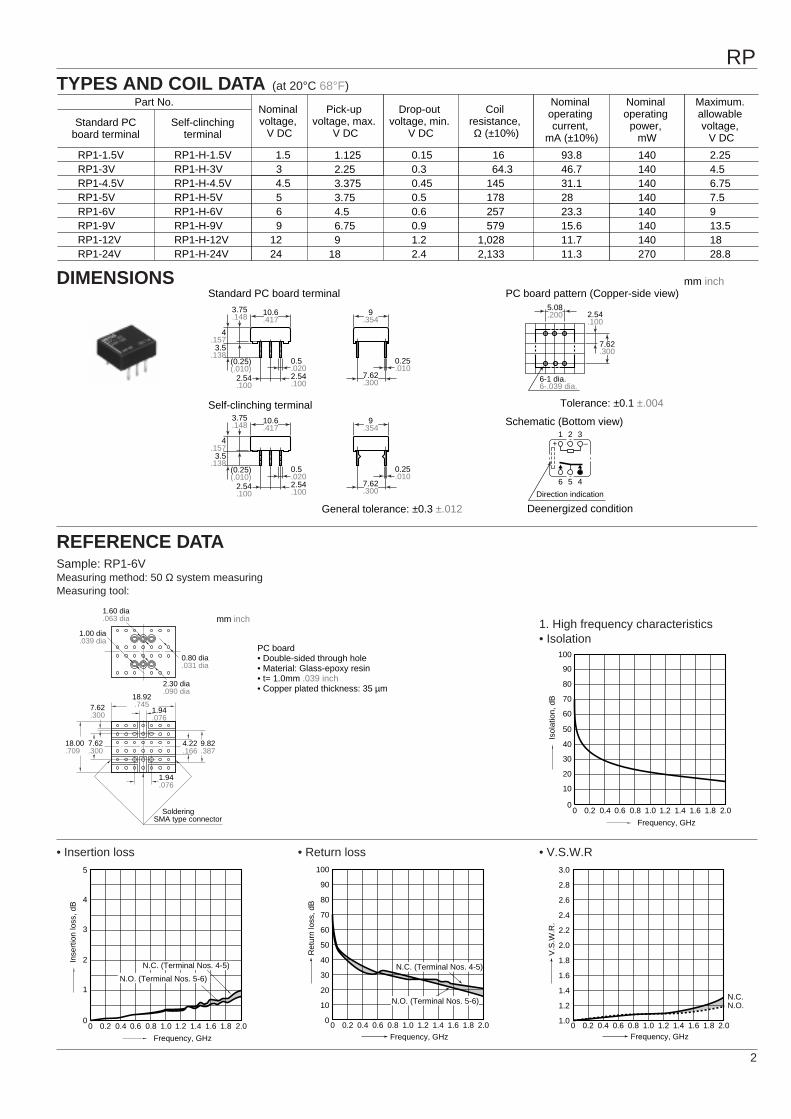
TYPES AND COIL DATA (at 20°C 68°F)
DIMENSIONS
Part No.
RP1-1.5V RP1-H-1.5VRP1-3V RP1-H-3VRP1-4.5V RP1-H-4.5VRP1-5V RP1-H-5VRP1-6V RP1-H-6VRP1-9V RP1-H-9VRP1-12V RP1-H-12VRP1-24V RP1-H-24V
1.534.5569
1224
0.150.30.450.50.60.91.22.4
1664.3
145178257579
1,0282,133
93.846.731.12823.315.611.711.3
2.254.56.757.5913.51828.8
140140140140140140140270
1.1252.253.3753.754.56.759
18
Nominal voltage,
V DCStandard PC
board terminalSelf-clinching
terminal
Pick-up voltage, max.
V DC
Drop-out voltage, min.
V DC
Coil resistance, Ω (±10%)
Nominal operating current,
mA (±10%)
Nominal operating
power, mW
Maximum. allowable voltage,
V DC
RP
5.08.200
7.62.300
6-1 dia.6-.039 dia.
2.54.100
10.6.417
7.62.300
9.354
3.75.148
4.157
2.54.100
0.5.020
0.25.010
2.54.100
3.5.138
(0.25)(.010)
10.6.417
7.62.300
9.354
3.75.148
4.157
2.54.100
0.5.020
0.25.010
2.54.100
3.5.138
(0.25)(.010)
Deenergized conditionGeneral tolerance: ±0.3 ±.012
Self-clinching terminal
Schematic (Bottom view)
Standard PC board terminal PC board pattern (Copper-side view)mm inch
Tolerance: ±0.1 ±.004
Direction indication
1 2 3
6 5 4
–+
REFERENCE DATASample: RP1-6VMeasuring method: 50 Ω system measuringMeasuring tool:
1.60 dia.063 dia
1.00 dia.039 dia
2.30 dia.090 dia
0.80 dia.031 dia
18.92.7457.62
.3001.94.076
4.22.166
1.94.076
7.62.300
18.00.709
9.82.387
SolderingSMA type connector
PC board• Double-sided through hole• Material: Glass-epoxy resin• t= 1.0mm .039 inch• Copper plated thickness: 35 µm
mm inch
1
2
3
4
5
0.80 0.4 1.00
1.81.61.41.20.60.2 2.0
Frequency, GHz
Inse
rtio
n lo
ss, d
B
N.C. (Terminal Nos. 4-5)
N.O. (Terminal Nos. 5-6)
• Return loss
Frequency, GHz
Ret
urn
loss
, dB
0 0.2 0.4 0.6 0.8 1.0 1.2 1.4 1.6 1.8 2.0
N.O. (Terminal Nos. 5-6)
N.C. (Terminal Nos. 4-5)
0
10
20
30
40
50
60
70
80
90
100
• V.S.W.R
Frequency, GHz
V.S
.W.R
.
0 0.2 0.4 0.6 0.8 1.0 1.2 1.4 1.6 1.8 2.0
N.C.N.O.
1.0
1.2
1.4
1.6
1.8
2.0
2.2
2.4
2.6
2.8
3.0
1. High frequency characteristics• Isolation
10
20
40
50
60
80
100
0.80 0.4 1.0
30
70
90
01.81.61.41.20.60.2 2.0
Frequency, GHz
Isol
atio
n, d
B
• Insertion loss
3
RP
10
30
60
70
80
100
80 100 120 1500
20
40
90
50
Coil applied voltage, %V
Tem
pera
ture
ris
e, °
C
3. Operate/release timeSample: RP1-9V; No. of samples: n = 50
• With diode
2
4
6
8
10
12
70 80 100 120 1500
Max.Max.Min.Min.
Coil applied voltage, %V
Tim
e, m
s
Operate time Release time
• Without diode
2
4
6
8
10
12
70 80 100 120 1500
Max.Min.Max.Min.
Coil applied voltage, %V
Tim
e, m
s
Operate time Release time
2. Coil temperature riseSample: RP1-6V; No. of samples: n = 5Carrying current: 0.1 AAmbient temperature: 25 to 70˚C 77 to 158˚F
2
4
6
8
10
12
100 1,00050050
Max.
Max.Min.
Min.
No. of operations, ×104
Pic
k-up
/dro
p-ou
t vol
tage
, V
Pick-up voltage
Drop-out voltage
5. Electrical life (0.1 A 30 V DC)Sample: RP1-6V; No. of samples: n = 6
• Change of pick-up/drop-out voltage
2
4
6
8
10
12
3020100
Max.
Max.Min.
Min.
No. of operations, ×104
Pic
k-up
/dro
p-ou
t vol
tage
, V
Pick-up voltage
Drop-out voltage
• Change of contact resistance
20
40
60
80
100
120
3020100
Max.Min.
No. of operations, ×104C
onta
ct r
esis
tanc
e, m
Ω
4. Mechanical lifeSample: RP1-5V; No. of samples: n = 8
• Change of pick-up, drop-out voltage
–40
40
20
–40 –20 0 20 40 60 80
Rat
e of
cha
nge,
%
Drop-outvoltage
Pick-upvoltage
Ambienttemperature, °C–20
10
20
40
50
2824 30
30
0383634322622 40
Contact resistance, mΩ
Qua
ntity
6. Ambient temperature characteristicsSample: RP1-6V; No. of samples: n = 5
7. Contact resistance distribution (initial)Sample: RP1-6V; No. of samples: n = 50
–5
10.394
5.197
0
0
5
–5
0
5 OFF
OFF
OFF
ON
ON
ON
Inter-relay distance, R (mm, inch)
Rat
e of
cha
nge,
%R
ate
of c
hang
e, %
Pick-up voltage
Drop-out voltage
R
R
R
R
OFF OFF
OFF
ON ON
ON–5
10.394
5.197
0
0
5
–5
0
5
Inter-relay distance, R (mm, inch)
Rat
e of
cha
nge,
%R
ate
of c
hang
e, %
Pick-up voltage
Drop-out voltage
R R
R R
OFF
ON
–5
10.394
5.197
0
0
5
–5
0
5
Inter-relay distance, R (mm, inch)
Rat
e of
cha
nge,
%R
ate
of c
hang
e, %
Pick-up voltage
Drop-out voltage
R R
R R
8.-(1) Influence of adjacent mountingSample: RP1-12V; No. of samples: n = 6
8.-(2) Influence of adjacent mountingSample: RP1-12V; No. of samples: n = 6
8.-(3) Influence of adjacent mountingSample: RP1-12V; No. of samples: n = 6
4
NOTES1. Packing directionRelays are packed in a tube with theorientation stripe (PIN NO. 1) toward thegreen stopper.
2. Automatic mountingTo maintain the internal function of therelay, the chucking pressure should not exceed the values below.
T1 T2
T1
T20.2s 0.2s
1.5s 1.5s
OFF
Trans-mission
Dummy load (50Ω) WD-2351Transmission: RF Tranceiver IC-1201 (ICOH)
ON
RP relay
• Change of pick-up/drop-out voltage
2
4
6
8
10
12
151050
Max.
Max.Min.
Min.
No. of operations, ×104
Pic
k-up
/dro
p-ou
t vol
tage
, V
Pick-up voltage
Drop-out voltage
• Change of contact resistance
20
40
60
80
100
120
151050
Max.Min.
No. of operations, ×104
Con
tact
res
ista
nce,
mΩ
9. High frequency switching test (1.2 GHz, 1 W)Sample: RP1-6V; No. of samples: n = 6Ambient temperature: 20˚C 68˚F
RP
Temperature 100˚C 212˚F or less
Within 1 minuteTimeOrientation (indicates PIN No. 1) stripe
Stopper (green)
A C B• Direction A • Direction B • Direction C
mm inch
5 46
2 3
3.1186.236
11 23
(4)(5)
(6)
*Value of chucking pressure is shown by the value of weightpressed on the portion (4 mm .157 inch dia.).
For Cautions for Use, please download ”Relay Technical Information“ - RTI.pdfYou´ll find ”RTI.pdf” in the download section of our web pages.
Chucking pressure* in the direction A:4.9 N 500 gf or less
Chucking pressure* in the direction B:9.8 N 1 kgf or less
Chucking pressure* in the direction C:9.8 N 1 kgf or less
3. SolderingPreheat according to the followingconditions.
Soldering should be done at 250˚C482˚F within 5 s.
© 1998 Matsushita Automation Controls Group EuropePDF-File generated January 1998, Data published may change due to technical improvements
10 V PrecisionVoltage Reference
REF01
Rev. G Information furnished by Analog Devices is believed to be accurate and reliable. However, no responsibility is assumed by Analog Devices for its use, nor for any infringements of patents or other rights of third parties that may result from its use. Specifications subject to change without notice. No license is granted by implication or otherwise under any patent or patent rights of Analog Devices. Trademarks and registered trademarks are the property of their respective owners.
One Technology Way, P.O. Box 9106, Norwood, MA 02062-9106, U.S.A. Tel: 781.329.4700 www.analog.com Fax: 781.326.8703 © 2005 Analog Devices, Inc. All rights reserved.
FEATURES
10 V output, ±0.3% max Adjustment range, ±3% min Excellent temperature stability, 8.5 ppm/°C max Low noise, 30 µV p-p max Low supply current, 1.4 mA max Wide input voltage range, 12 V to 40 V High load driving capability, 10 mA No external components Short-circuit proof
GENERAL DESCRIPTION The REF01 precision voltage reference provides a stable 10 V output that can be adjusted over a 3% range with minimal effect on temperature stability. Single-supply operation over an input voltage range of 12 V to 40 V, a low current drain of 1 mA, and excellent temperature stability are achieved with an improved band gap design. Low cost, low noise, and low power make the REF01 an excellent choice whenever a stable voltage reference is required. Applications include DACs and ADCs, portable instrumentation, and digital voltmeters. Full military temperature range devices with screening to MIL-STD-883 are available. For new designs, refer to ADR01.
PIN CONFIGURATIONS
0037
3-F-
001
1
2
34
5
6
78
NC
GROUND(CASE)
NC
VIN VOUT
NC
NC TRIM
NC = NO CONNECT. DO NOT CONNECT ANYTHINGON THESE PINS. SOME OF THEM ARE RESERVEDFOR FACTORY TESTING PURPOSES.
Figure 1. TO-99 (J Suffix)
0037
3-F-
002
REF01TOP VIEW
(Not to Scale)
NC 1
VIN 2
NC 3
GND 4
NCNCVOUT
TRIM
8
7
6
5
NC = NO CONNECT. DO NOT CONNECT ANYTHINGON THESE PINS. SOME OF THEM ARE RESERVEDFOR FACTORY TESTING PURPOSES.
Figure 2. 8-Lead PDIP (P-Suffix) 8-Lead CERDIP (Z-Suffix)
8-Lead SOIC (S-Suffix)
0037
3-F-
003
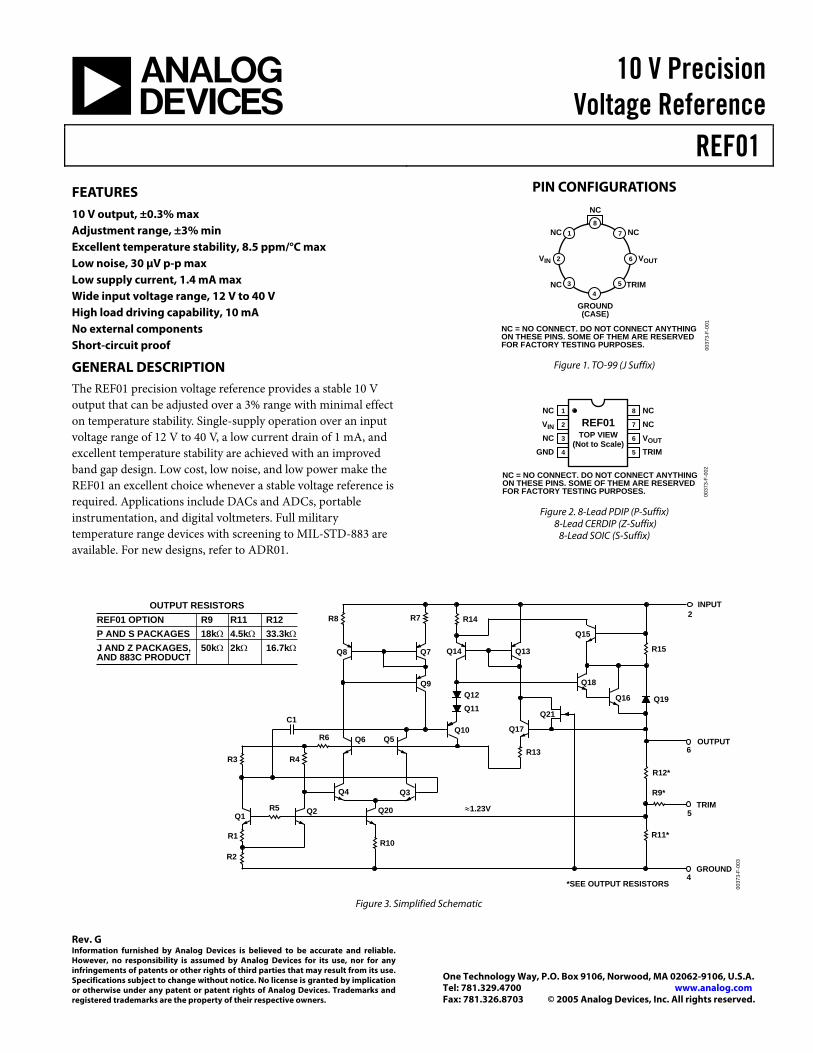
REF01 OPTION R9 R11 R12P AND S PACKAGES 18kΩ 4.5kΩ 33.3kΩJ AND Z PACKAGES, 50kΩ 2kΩ 16.7kΩAND 883C PRODUCT
OUTPUT RESISTORS
C1
R3
R6
R4
R5
R1
Q1
R2R10
OUTPUT
GROUND
R12*
TRIM
Q19
R15
INPUT
Q15
Q18
Q16
Q13
Q21
Q17
R13
Q20
Q4 Q3
Q5Q6
Q9
Q7 Q14
Q12Q11
Q8
R8 R7 R14
Q10
Q2
R11*
R9*
4
5
6
≈1.23V
2
*SEE OUTPUT RESISTORS
Figure 3. Simplified Schematic
REF01
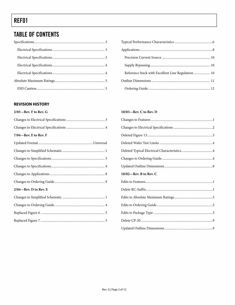
Rev. G | Page 2 of 12
TABLE OF CONTENTS Specifications..................................................................................... 3
Electrical Specifications............................................................... 3
Electrical Specifications............................................................... 3
Electrical Specifications............................................................... 4
Electrical Specifications............................................................... 4
Absolute Maximum Ratings............................................................ 5
ESD Caution.................................................................................. 5
Typical Performance Characteristics ..............................................6
Applications........................................................................................8
Precision Current Source .......................................................... 10
Supply Bypassing ........................................................................ 10
Reference Stack with Excellent Line Regulation .................... 10
Outline Dimensions ....................................................................... 11
Ordering Guide .......................................................................... 12
REVISION HISTORY
2/05—Rev. F to Rev. G
Changes to Electrical Specifications .............................................. 3
Changes to Electrical Specifications .............................................. 4
7/04—Rev. E to Rev. F
Updated Format..................................................................Universal
Changes to Simplified Schematic ................................................... 1
Changes to Specifications ................................................................ 3
Changes to Specifications ................................................................ 4
Changes to Applications .................................................................. 8
Changes to Ordering Guide ............................................................ 9
2/04—Rev. D to Rev. E
Changes to Simplified Schematic .................................................. 1
Changes to Ordering Guide ............................................................ 4
Replaced Figure 6 ............................................................................. 5
Replaced Figure 7 ............................................................................. 5
10/03—Rev. C to Rev. D
Changes to Features ..........................................................................1
Changes to Electrical Specifications ...............................................2
Deleted Figure 13...............................................................................3
Deleted Wafer Test Limits ................................................................4
Deleted Typical Electrical Characteristics......................................4
Changes to Ordering Guide .............................................................4
Updated Outline Dimensions..........................................................8
10/02—Rev. B to Rev. C
Edits to Features.................................................................................1
Delete RC-Suffix................................................................................1
Edits to Absolute Maximum Ratings ..............................................5
Edits to Ordering Guide ...................................................................5
Edits to Package Type .......................................................................5
Delete CP-20 ......................................................................................9
Updated Outline Dimensions..........................................................9
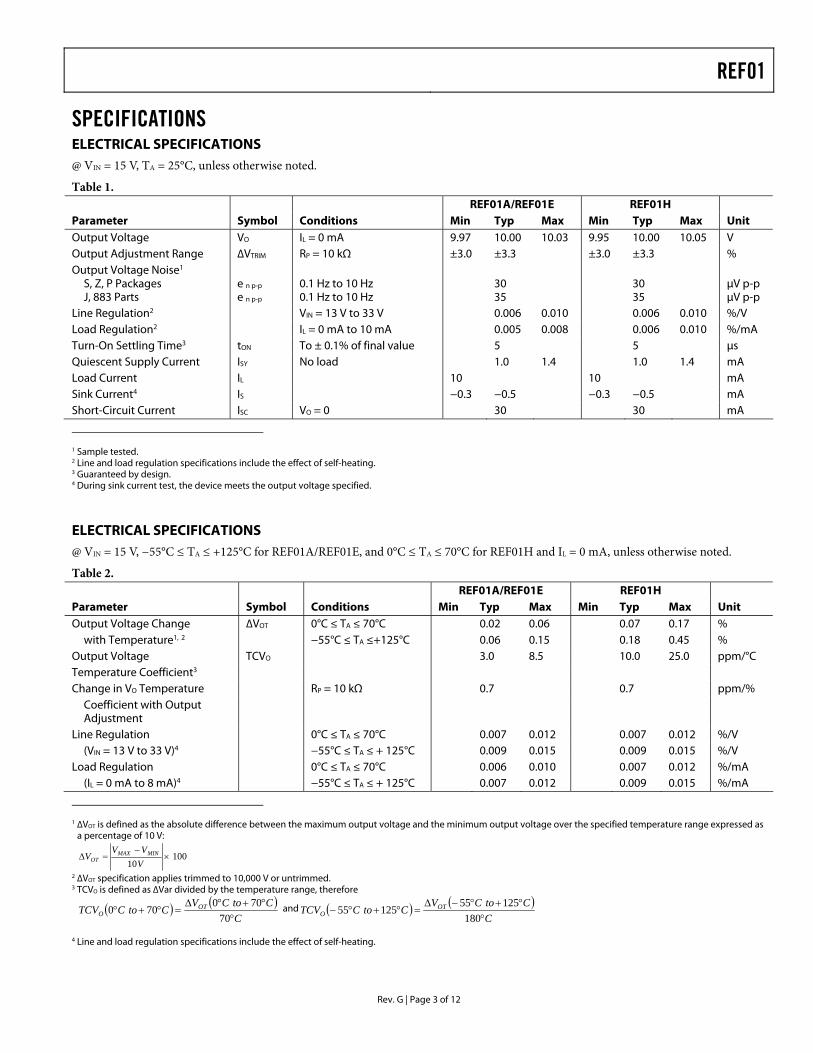
REF01
Rev. G | Page 3 of 12
SPECIFICATIONS ELECTRICAL SPECIFICATIONS @ VIN = 15 V, TA = 25°C, unless otherwise noted.
Table 1. REF01A/REF01E REF01H Parameter Symbol Conditions Min Typ Max Min Typ Max Unit Output Voltage VO IL = 0 mA 9.97 10.00 10.03 9.95 10.00 10.05 V Output Adjustment Range ∆VTRIM RP = 10 kΩ ±3.0 ±3.3 ±3.0 ±3.3 % Output Voltage Noise1
S, Z, P Packages J, 883 Parts
e n p-p
e n p-p
0.1 Hz to 10 Hz 0.1 Hz to 10 Hz
30 35
30 35
µV p-p µV p-p
Line Regulation2 VIN = 13 V to 33 V 0.006 0.010 0.006 0.010 %/V Load Regulation2 IL = 0 mA to 10 mA 0.005 0.008 0.006 0.010 %/mA Turn-On Settling Time3 tON To ± 0.1% of final value 5 5 µs Quiescent Supply Current ISY No load 1.0 1.4 1.0 1.4 mA Load Current IL 10 10 mA Sink Current4 IS −0.3 −0.5 −0.3 −0.5 mA Short-Circuit Current ISC VO = 0 30 30 mA
1 Sample tested. 2 Line and load regulation specifications include the effect of self-heating. 3 Guaranteed by design. 4 During sink current test, the device meets the output voltage specified.
ELECTRICAL SPECIFICATIONS @ VIN = 15 V, −55°C ≤ TA ≤ +125°C for REF01A/REF01E, and 0°C ≤ TA ≤ 70°C for REF01H and IL = 0 mA, unless otherwise noted.
Table 2. REF01A/REF01E REF01H Parameter Symbol Conditions Min Typ Max Min Typ Max Unit Output Voltage Change ∆VOT 0°C ≤ TA ≤ 70°C 0.02 0.06 0.07 0.17 %
with Temperature1, 2 −55°C ≤ TA ≤+125°C 0.06 0.15 0.18 0.45 % Output Voltage TCVO 3.0 8.5 10.0 25.0 ppm/°C Temperature Coefficient3 Change in VO Temperature RP = 10 kΩ 0.7 0.7 ppm/%
Coefficient with Output Adjustment
Line Regulation 0°C ≤ TA ≤ 70°C 0.007 0.012 0.007 0.012 %/V (VIN = 13 V to 33 V)4 −55°C ≤ TA ≤ + 125°C 0.009 0.015 0.009 0.015 %/V
Load Regulation 0°C ≤ TA ≤ 70°C 0.006 0.010 0.007 0.012 %/mA (IL = 0 mA to 8 mA)4 −55°C ≤ TA ≤ + 125°C 0.007 0.012 0.009 0.015 %/mA
1 ∆VOT is defined as the absolute difference between the maximum output voltage and the minimum output voltage over the specified temperature range expressed as
a percentage of 10 V:
10010
×−
=∆VVV
V MINMAXOT
2 ∆VOT specification applies trimmed to 10,000 V or untrimmed. 3 TCVO is defined as ∆Var divided by the temperature range, therefore
( ) ( )C
CtoCVCtoCTCV OT
O °°+°∆
=°+°70
700700 and ( ) ( )
CCtoCV
CtoCTCV OTO °
°+°−∆=°+°−
18012555
12555
4 Line and load regulation specifications include the effect of self-heating.
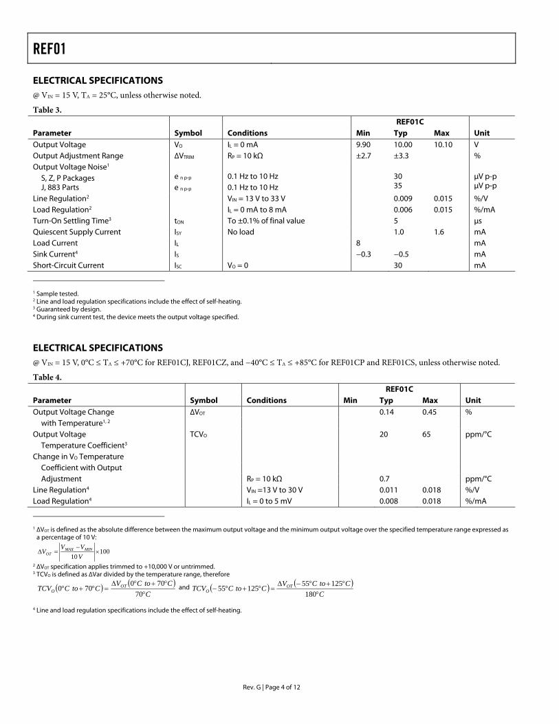
REF01
Rev. G | Page 4 of 12
ELECTRICAL SPECIFICATIONS @ VIN = 15 V, TA = 25°C, unless otherwise noted.
Table 3. REF01C Parameter Symbol Conditions Min Typ Max Unit Output Voltage VO IL = 0 mA 9.90 10.00 10.10 V Output Adjustment Range ∆VTRIM RP = 10 kΩ ±2.7 ±3.3 % Output Voltage Noise1
S, Z, P Packages J, 883 Parts
e n p-p e n p-p
0.1 Hz to 10 Hz 0.1 Hz to 10 Hz
30 35
µV p-p µV p-p
Line Regulation2 VIN = 13 V to 33 V 0.009 0.015 %/V Load Regulation2 IL = 0 mA to 8 mA 0.006 0.015 %/mA Turn-On Settling Time3 tON To ±0.1% of final value 5 µs Quiescent Supply Current ISY No load 1.0 1.6 mA Load Current IL 8 mA Sink Current4 IS −0.3 −0.5 mA Short-Circuit Current ISC VO = 0 30 mA
1 Sample tested. 2 Line and load regulation specifications include the effect of self-heating. 3 Guaranteed by design. 4 During sink current test, the device meets the output voltage specified.
ELECTRICAL SPECIFICATIONS @ VIN = 15 V, 0°C ≤ TA ≤ +70°C for REF01CJ, REF01CZ, and −40°C ≤ TA ≤ +85°C for REF01CP and REF01CS, unless otherwise noted.
Table 4. REF01C Parameter Symbol Conditions Min Typ Max Unit Output Voltage Change ∆VOT 0.14 0.45 %
with Temperature1, 2 Output Voltage TCVO 20 65 ppm/°C
Temperature Coefficient3 Change in VO Temperature
Coefficient with Output Adjustment RP = 10 kΩ 0.7 ppm/°C
Line Regulation4 VIN =13 V to 30 V 0.011 0.018 %/V Load Regulation4 IL = 0 to 5 mV 0.008 0.018 %/mA
1 ∆VOT is defined as the absolute difference between the maximum output voltage and the minimum output voltage over the specified temperature range expressed as
a percentage of 10 V:
10010
×−
=∆VVV
V MINMAXOT
2 ∆VOT specification applies trimmed to +10,000 V or untrimmed. 3 TCVO is defined as ∆Var divided by the temperature range, therefore
( ) ( )C
CtoCVCtoCTCV OT
O °°+°∆
=°+°70
700700 and ( ) ( )
CCtoCV
CtoCTCV OTO °
°+°−∆=°+°−
18012555
12555
4 Line and load regulation specifications include the effect of self-heating.
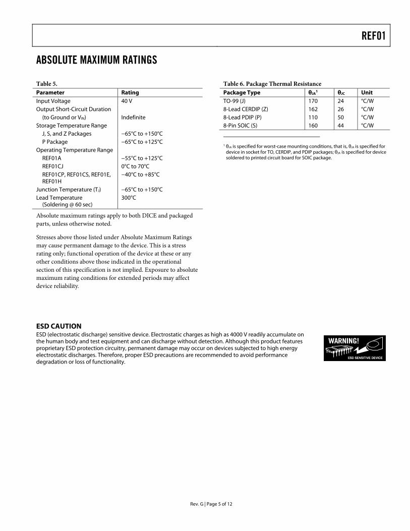
REF01
Rev. G | Page 5 of 12
ABSOLUTE MAXIMUM RATINGS
Table 5. Parameter Rating Input Voltage 40 V Output Short-Circuit Duration
(to Ground or VIN) Indefinite Storage Temperature Range
J, S, and Z Packages −65°C to +150°C P Package −65°C to +125°C
Operating Temperature Range REF01A −55°C to +125°C REF01CJ 0°C to 70°C REF01CP, REF01CS, REF01E, REF01H
−40°C to +85°C
Junction Temperature (TJ) −65°C to +150°C Lead Temperature
(Soldering @ 60 sec) 300°C
Absolute maximum ratings apply to both DICE and packaged parts, unless otherwise noted.
Stresses above those listed under Absolute Maximum Ratings may cause permanent damage to the device. This is a stress rating only; functional operation of the device at these or any other conditions above those indicated in the operational section of this specification is not implied. Exposure to absolute maximum rating conditions for extended periods may affect device reliability.
Table 6. Package Thermal Resistance Package Type θJA
1 θJC Unit TO-99 (J) 170 24 °C/W 8-Lead CERDIP (Z) 162 26 °C/W 8-Lead PDIP (P) 110 50 °C/W 8-Pin SOIC (S) 160 44 °C/W
1 θJA is specified for worst-case mounting conditions, that is, θJA is specified for
device in socket for TO, CERDIP, and PDIP packages; θJA is specified for device soldered to printed circuit board for SOIC package.
ESD CAUTION ESD (electrostatic discharge) sensitive device. Electrostatic charges as high as 4000 V readily accumulate on the human body and test equipment and can discharge without detection. Although this product features proprietary ESD protection circuitry, permanent damage may occur on devices subjected to high energy electrostatic discharges. Therefore, proper ESD precautions are recommended to avoid performance degradation or loss of functionality.
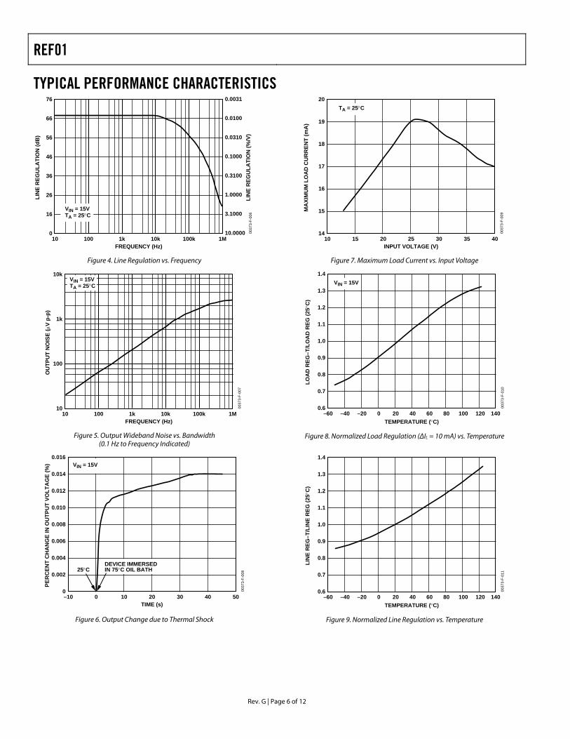
REF01
Rev. G | Page 6 of 12
TYPICAL PERFORMANCE CHARACTERISTICS 76
0
16
26
36
46
56
66
10 100 1k 10k 100k 1M
0037
3-F-
006
FREQUENCY (Hz)
LIN
E R
EGU
LATI
ON
(dB
)
LIN
E R
EGU
LATI
ON
(%/V
)
VIN = 15VTA = 25°C
0.0031
0.0100
0.0310
0.1000
0.3100
1.0000
3.1000
10.0000
Figure 4. Line Regulation vs. Frequency
10k
1k
100
1010 100 1k 10k 100k 1M
0037
3-F-
007
FREQUENCY (Hz)
OU
TPU
T N
OIS
E (µ
V p-
p)
VIN = 15VTA = 25°C
Figure 5. Output Wideband Noise vs. Bandwidth (0.1 Hz to Frequency Indicated)
0.016
0.014
0.012
0.010
0.008
0.006
0.004
0.002
0–10 0 10 20 30 40 50
0037
3-F-
008
TIME (s)
PER
CEN
T C
HA
NG
E IN
OU
TPU
T VO
LTA
GE
(%) VIN = 15V
25°CDEVICE IMMERSEDIN 75°C OIL BATH
Figure 6. Output Change due to Thermal Shock
20
15
16
17
18
19
1410 15 20 25 30 35 40
0037
3-F-
009
INPUT VOLTAGE (V)
MA
XIM
UM
LO
AD
CU
RR
ENT
(mA
)
TA = 25°C
Figure 7. Maximum Load Current vs. Input Voltage
1.4
1.3
1.2
1.1
1.0
0.9
0.8
0.7
0.6–60 –40 –20 0 20 40 60 80 100 120 140
0037
3-F-
010
TEMPERATURE (°C)
LOA
D R
EG–T
/LO
AD
REG
(25°
C)
VIN = 15V
Figure 8. Normalized Load Regulation (∆IL = 10 mA) vs. Temperature
1.4
1.3
1.2
1.1
1.0
0.9
0.8
0.7
0.6–60 –40 –20 0 20 40 60 80 100 120 140
0037
3-F-
011
TEMPERATURE (°C)
LIN
E R
EG–T
/LIN
E R
EG (2
5°C
)
Figure 9. Normalized Line Regulation vs. Temperature
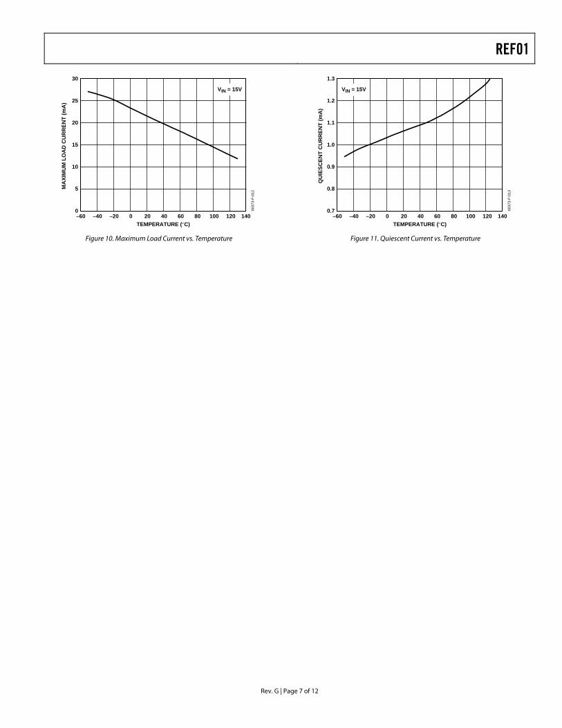
REF01
Rev. G | Page 7 of 12
30
25
20
15
10
5
0–60 –40 –20 0 20 40 60 80 100 120 140
0037
3-F-
012
TEMPERATURE (°C)
MA
XIM
UM
LO
AD
CU
RR
ENT
(mA
)
VIN = 15V
Figure 10. Maximum Load Current vs. Temperature
1.3
1.2
1.1
1.0
0.9
0.8
0.7–60 –40 –20 0 20 40 60 80 100 120 140
0037
3-F-
013
TEMPERATURE (°C)
QU
IESC
ENT
CU
RR
ENT
(mA
)
VIN = 15V
Figure 11. Quiescent Current vs. Temperature
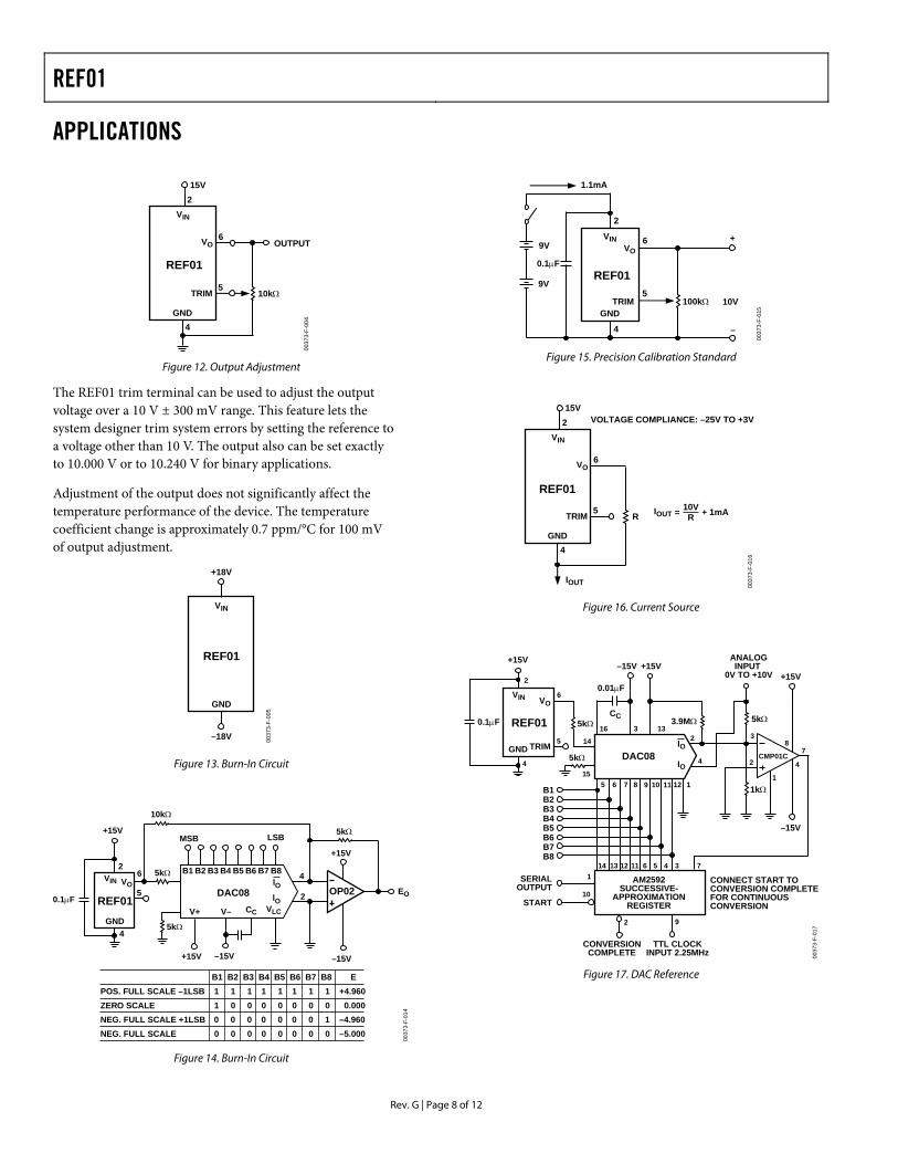
REF01
Rev. G | Page 8 of 12
APPLICATIONS
0037
3-F-
004
VIN
GND
TRIM
VO
REF01
15V2
6
5
4
OUTPUT
10kΩ
Figure 12. Output Adjustment
The REF01 trim terminal can be used to adjust the output voltage over a 10 V ± 300 mV range. This feature lets the system designer trim system errors by setting the reference to a voltage other than 10 V. The output also can be set exactly to 10.000 V or to 10.240 V for binary applications.
Adjustment of the output does not significantly affect the temperature performance of the device. The temperature coefficient change is approximately 0.7 ppm/°C for 100 mV of output adjustment.
0037
3-F-
005
VIN
GND
–18V
+18V
REF01
Figure 13. Burn-In Circuit
0037
3-F-
014
REF01DAC08 OP02
0.1µF
+15V
4
6
5
10kΩ
5kΩ
5kΩ
5kΩ
+15V –15V –15V
+15V
EO
LSBMSB
2 B1 B2 B3 B4 B5 B6 B7 B8
V+ V– CC VLC
lO 2
4lO
B1 B2 B3 B4 B5 B6 B7 B8 EPOS. FULL SCALE –1LSB 1 1 1 1 1 1 1 1 +4.960ZERO SCALE 1 0 0 0 0 0 0 0 0.000NEG. FULL SCALE +1LSB 0 0 0 0 0 0 0 1 –4.960NEG. FULL SCALE 0 0 0 0 0 0 0 0 –5.000
VIN VO
GND
Figure 14. Burn-In Circuit
0037
3-F-
015GND
REF01
VO
VIN
TRIM
+
–
10V100kΩ
1.1mA
2
6
5
4
9V
9V
0.1µF
Figure 15. Precision Calibration Standard
0037
3-F-
016
VIN
GND
TRIM
VO
REF01
15V2
6
5
4
R
IOUT
IOUT = 10VR + 1mA
VOLTAGE COMPLIANCE: –25V TO +3V
Figure 16. Current Source
0037
3-F-
017
2
+15V
4DAC08
+15V
3.9MΩ 5kΩREF01
5kΩ
5kΩ
1kΩ
–15V +15V
–15V
SERIALOUTPUT
START
CONVERSIONCOMPLETE
TTL CLOCKINPUT 2.25MHz
CONNECT START TOCONVERSION COMPLETEFOR CONTINUOUSCONVERSION
0.1µF
0.01µF
B1B2B3B4B5B6B7B8
5
6
14
15765 8 9 10 11 12 1
3456111213141
10
2 9
7
2
4
3
2
1
4
78
16
GND
VIN VOCC
IO
IO
3 13
CMP01CTRIM
ANALOGINPUT
0V TO +10V
AM2592SUCCESSIVE-
APPROXIMATIONREGISTER
Figure 17. DAC Reference
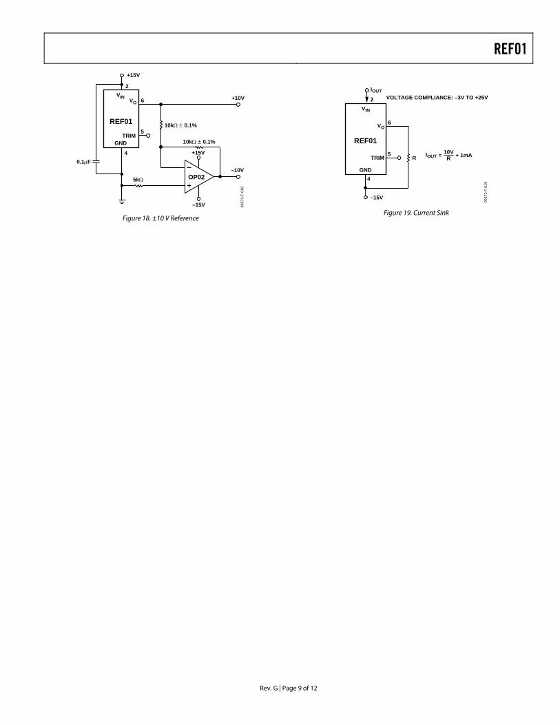
REF01
Rev. G | Page 9 of 12
0037
3-F-
018
VIN
GND
REF01
VO
TRIM
0.1µF
5kΩ OP02
10kΩ ± 0.1%
10kΩ ± 0.1%
+15V
–15V
+15V
+10V
–10V
4
5
6
2
Figure 18. ±10 V Reference
0037
3-F-
019
VIN
GND
TRIM
VO
REF01
–15V
2
6
5
4
R
IOUT
IOUT = 10VR + 1mA
VOLTAGE COMPLIANCE: –3V TO +25V
Figure 19. Current Sink
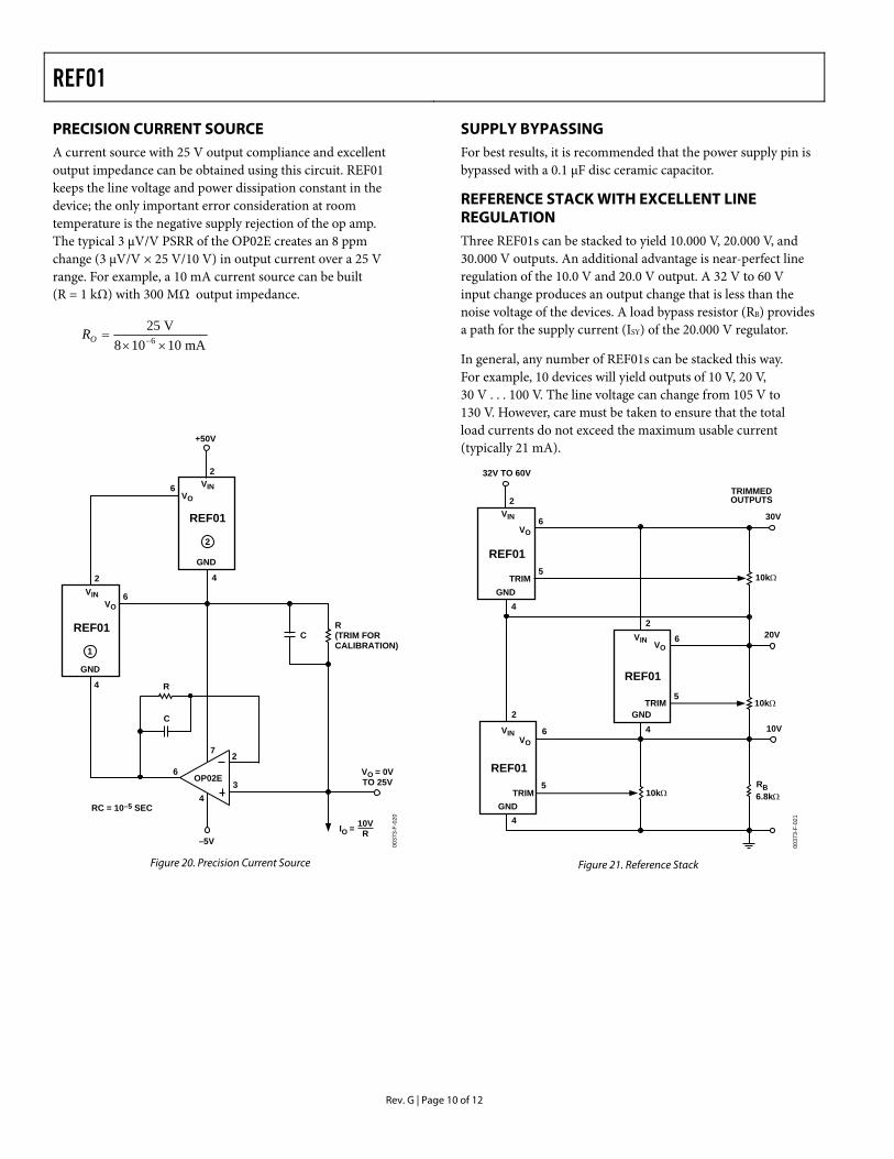
REF01
Rev. G | Page 10 of 12
PRECISION CURRENT SOURCE A current source with 25 V output compliance and excellent output impedance can be obtained using this circuit. REF01 keeps the line voltage and power dissipation constant in the device; the only important error consideration at room temperature is the negative supply rejection of the op amp. The typical 3 µV/V PSRR of the OP02E creates an 8 ppm change (3 µV/V × 25 V/10 V) in output current over a 25 V range. For example, a 10 mA current source can be built (R = 1 kΩ) with 300 MΩ output impedance.
mA10108V25
6 ××= −OR
00
373-
F-02
0
GND
REF01
GND
REF01
OP02E
C
C
R
2
2
2
6
6
7
34
6
4
4
+50V
–5VIO = 10V
R
RC = 10–5 SEC
R(TRIM FORCALIBRATION)
VINVO
VINVO
VO = 0VTO 25V
1
2
Figure 20. Precision Current Source
SUPPLY BYPASSING For best results, it is recommended that the power supply pin is bypassed with a 0.1 µF disc ceramic capacitor.
REFERENCE STACK WITH EXCELLENT LINE REGULATION Three REF01s can be stacked to yield 10.000 V, 20.000 V, and 30.000 V outputs. An additional advantage is near-perfect line regulation of the 10.0 V and 20.0 V output. A 32 V to 60 V input change produces an output change that is less than the noise voltage of the devices. A load bypass resistor (RB) provides a path for the supply current (ISY) of the 20.000 V regulator.
In general, any number of REF01s can be stacked this way. For example, 10 devices will yield outputs of 10 V, 20 V, 30 V . . . 100 V. The line voltage can change from 105 V to 130 V. However, care must be taken to ensure that the total load currents do not exceed the maximum usable current (typically 21 mA).
0037
3-F-
021
GND
REF01
GND
REF01
GND
REF01
TRIM
TRIM
10kΩ
10kΩ
RB6.8kΩ10kΩ
2
6
5
4
2
6
5
4
2
6
5
4
30V
20V
10V
TRIM
32V TO 60V
TRIMMEDOUTPUTS
VIN VO
VIN
VO
VINVO
Figure 21. Reference Stack
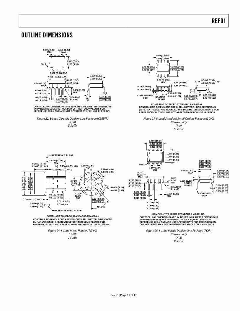
REF01
Rev. G | Page 11 of 12
OUTLINE DIMENSIONS
CONTROLLING DIMENSIONS ARE IN INCHES; MILLIMETER DIMENSIONS(IN PARENTHESES) ARE ROUNDED-OFF INCH EQUIVALENTS FORREFERENCE ONLY AND ARE NOT APPROPRIATE FOR USE IN DESIGN
1 4
8 5
0.310 (7.87)0.220 (5.59)PIN 1
0.005 (0.13)MIN
0.055 (1.40)MAX
0.100 (2.54) BSC
15° 0°
0.320 (8.13)0.290 (7.37)
0.015 (0.38)0.008 (0.20)
SEATINGPLANE
0.200 (5.08)MAX
0.405 (10.29) MAX
0.150 (3.81)MIN
0.200 (5.08)0.125 (3.18)
0.023 (0.58)0.014 (0.36)
0.070 (1.78)0.030 (0.76)
0.060 (1.52)0.015 (0.38)
0.25 (0.0098)0.17 (0.0067)
1.27 (0.0500)0.40 (0.0157)
0.50 (0.0196)0.25 (0.0099) × 45°
8°0°
1.75 (0.0688)1.35 (0.0532)
SEATINGPLANE
0.25 (0.0098)0.10 (0.0040)
41
8 5
5.00 (0.1968)4.80 (0.1890)
4.00 (0.1574)3.80 (0.1497)
1.27 (0.0500)BSC
6.20 (0.2440)5.80 (0.2284)
0.51 (0.0201)0.31 (0.0122)COPLANARITY
0.10
CONTROLLING DIMENSIONS ARE IN MILLIMETERS; INCH DIMENSIONS(IN PARENTHESES) ARE ROUNDED-OFF MILLIMETER EQUIVALENTS FORREFERENCE ONLY AND ARE NOT APPROPRIATE FOR USE IN DESIGN
COMPLIANT TO JEDEC STANDARDS MS-012AA
Figure 22. 8-Lead Ceramic Dual In- Line Package [CERDIP]
(Q-8) Z-Suffix
Figure 23. 8-Lead Standard Small Outline Package [SOIC] Narrow Body
(R-8) S-Suffix
CONTROLLING DIMENSIONS ARE IN INCHES; MILLIMETER DIMENSIONS(IN PARENTHESES) ARE ROUNDED-OFF INCH EQUIVALENTS FORREFERENCE ONLY AND ARE NOT APPROPRIATE FOR USE IN DESIGN.
COMPLIANT TO JEDEC STANDARDS MO-002-AK
0.2500 (6.35) MIN
0.5000 (12.70)MIN0.1850 (4.70)
0.1650 (4.19)
REFERENCE PLANE
0.0500 (1.27) MAX
0.0190 (0.48)0.0160 (0.41)
0.0210 (0.53)0.0160 (0.41)0.0400 (1.02)
0.0100 (0.25)
0.0400 (1.02) MAX 0.0340 (0.86)0.0280 (0.71)
0.0450 (1.14)0.0270 (0.69)
0.1600 (4.06)0.1400 (3.56)
0.1000 (2.54)BSC
6
2 8
7
54
3
1
0.2000(5.08)BSC
0.1000(2.54)BSC
0.37
00 (9
.40)
0.33
50 (8
.51)
0.33
50 (8
.51)
0.30
50 (7
.75)
45° BSCBASE & SEATING PLANE
COMPLIANT TO JEDEC STANDARDS MS-001-BA
0.022 (0.56)0.018 (0.46)0.014 (0.36)
SEATINGPLANE
0.015(0.38)MIN
0.210(5.33)MAX
PIN 1
0.150 (3.81)0.130 (3.30)0.115 (2.92)
0.070 (1.78)0.060 (1.52)0.045 (1.14)
8
1 4
5 0.280 (7.11)0.250 (6.35)0.240 (6.10)
0.100 (2.54)BSC
0.400 (10.16)0.365 (9.27)0.355 (9.02)
0.060 (1.52)MAX
0.430 (10.92)MAX
0.014 (0.36)0.010 (0.25)0.008 (0.20)
0.325 (8.26)0.310 (7.87)0.300 (7.62)
0.195 (4.95)0.130 (3.30)0.115 (2.92)
0.015 (0.38)GAUGEPLANE
0.005 (0.13)MIN
CONTROLLING DIMENSIONS ARE IN INCHES; MILLIMETER DIMENSIONS(IN PARENTHESES) ARE ROUNDED-OFF INCH EQUIVALENTS FORREFERENCE ONLY AND ARE NOT APPROPRIATE FOR USE IN DESIGN.CORNER LEADS MAY BE CONFIGURED AS WHOLE OR HALF LEADS.
Figure 24. 8-Lead Metal Header [TO-99] (H-08)
J-Suffix
Figure 25. 8-Lead Plastic Dual In-Line Package [PDIP] Narrow Body
(N-8) P-Suffix
REF01
Rev. G | Page 12 of 12
ORDERING GUIDE Burn-in is available on commercial and industrial temperature range parts in CERDIP, PDIP, and TO-can packages.
TA = 25° C Model ∆VOS Max (mV) Operating Temperature Range (°C) Package Description Package Option REF01EJ ± 30 −40 to +85 TO-99 J-8 REF01CJ ± 100 0 to 70 TO-99 J-8 REF01EZ ± 30 −40 to +85 CERDIP Z-8 REF01HZ ± 50 −40 to +85 CERDIP Z-8 REF01AZ/883C ± 30 −55 to +125 CERDIP Z-8 REF01CP ± 100 −40 to +85 PDIP P-8 REF01CPZ1 ± 100 −40 to +85 PDIP P-8 REF01HPZ1 ± 50 −40 to +85 PDIP P-8 REF01HP ± 50 −40 to +85 PDIP P-8 REF01HS2 ± 50 −40 to +85 SOIC R-8 REF01HS-REEL ± 50 −40 to +85 SOIC R-8 REF01HSZ1 ± 50 −40 to +85 SOIC R-8 REF01HSZ-REEL1 ± 50 −40 to +85 SOIC R-8 REF01CS2 ± 100 −40 to +85 SOIC R-8 REF01CS-REEL ± 100 −40 to +85 SOIC R-8 REF01CS-REEL7 ± 100 −40 to +85 SOIC R-8 REF01CSZ-REEL1 ± 100 −40 to +85 SOIC R-8 REF01CSZ-REEL71 ± 100 −40 to +85 SOIC R-8 REF01CSZ ± 100 −40 to +85 SOIC R-8 REF01AJ/883C2 ± 30 −55 to +125 TO-99 J-8
1 Z = Pb-free part. 2 For availability and burn-in information on SOIC packages, contact your local sales office.
© 2005 Analog Devices, Inc. All rights reserved. Trademarks and registered trademarks are the property of their respective owners. C00373-0-2/05(G)
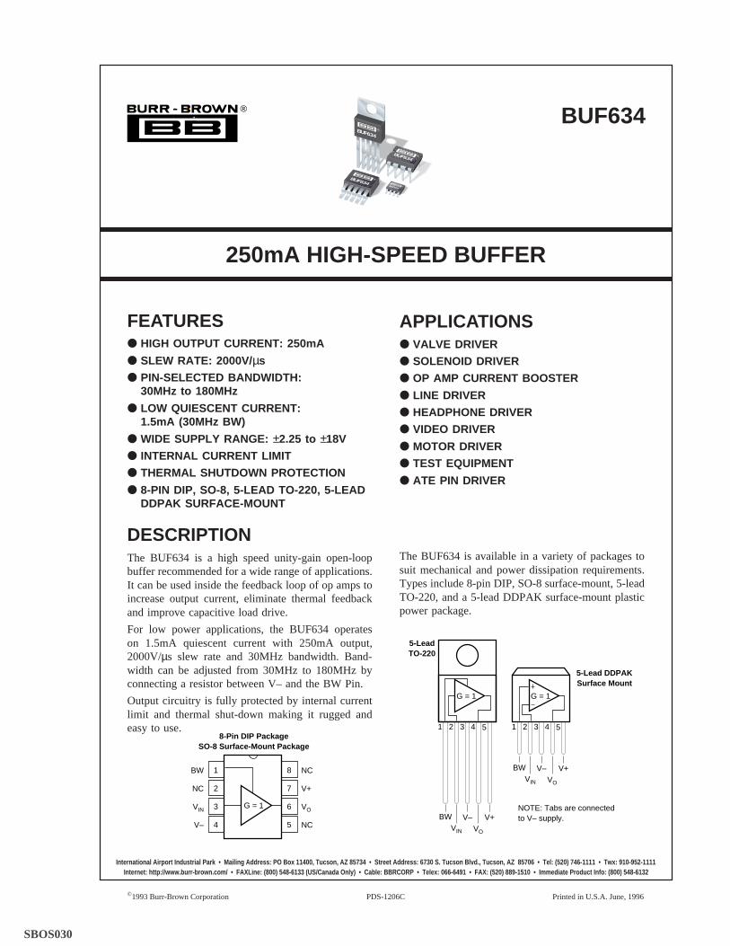
©1993 Burr-Brown Corporation PDS-1206C Printed in U.S.A. June, 1996
BUF634
FEATURES HIGH OUTPUT CURRENT: 250mA
SLEW RATE: 2000V/ µs
PIN-SELECTED BANDWIDTH:30MHz to 180MHz
LOW QUIESCENT CURRENT:1.5mA (30MHz BW)
WIDE SUPPLY RANGE: ±2.25 to ±18V
INTERNAL CURRENT LIMIT
THERMAL SHUTDOWN PROTECTION
8-PIN DIP, SO-8, 5-LEAD TO-220, 5-LEADDDPAK SURFACE-MOUNT
BW
NC
VIN
V–
NC
V+
VO
NC
1
2
3
4
8
7
6
5
8-Pin DIP PackageSO-8 Surface-Mount Package
G = 1
®
APPLICATIONS VALVE DRIVER
SOLENOID DRIVER
OP AMP CURRENT BOOSTER
LINE DRIVER
HEADPHONE DRIVER
VIDEO DRIVER
MOTOR DRIVER
TEST EQUIPMENT
ATE PIN DRIVER
DESCRIPTIONThe BUF634 is a high speed unity-gain open-loopbuffer recommended for a wide range of applications.It can be used inside the feedback loop of op amps toincrease output current, eliminate thermal feedbackand improve capacitive load drive.
For low power applications, the BUF634 operateson 1.5mA quiescent current with 250mA output,2000V/µs slew rate and 30MHz bandwidth. Band-width can be adjusted from 30MHz to 180MHz byconnecting a resistor between V– and the BW Pin.
Output circuitry is fully protected by internal currentlimit and thermal shut-down making it rugged andeasy to use.
The BUF634 is available in a variety of packages tosuit mechanical and power dissipation requirements.Types include 8-pin DIP, SO-8 surface-mount, 5-leadTO-220, and a 5-lead DDPAK surface-mount plasticpower package.
250mA HIGH-SPEED BUFFER
BUF634
BUF634
BUF634
BUF634
G = 1 G = 1
V–VO
V+VIN
BW
1 2 3 4 5
5-LeadTO-220
V–VO
V+VIN
BW
1 2 3 4 5
NOTE: Tabs are connectedto V– supply.
5-Lead DDPAKSurface Mount
International Airport Industrial Park • Mailing Address: PO Box 11400, Tucson, AZ 85734 • Street Address: 6730 S. Tucson Bl vd., Tucson, AZ 85706 • Tel: (520) 746-1111 • Twx: 910-952-1111Internet: http://www.burr-brown.com/ • FAXLine: (800) 548-6133 (US/Canada Only) • Cable: BBRCORP • Telex: 066-6491 • FA X: (520) 889-1510 • Immediate Product Info: (800) 548-6132
SBOS030
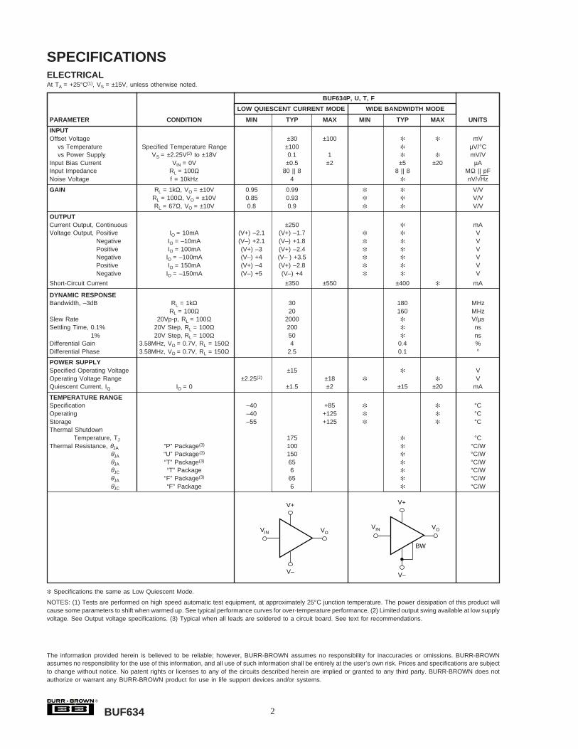
2®
BUF634
SPECIFICATIONSELECTRICAL
The information provided herein is believed to be reliable; however, BURR-BROWN assumes no responsibility for inaccuracies or omissions. BURR-BROWNassumes no responsibility for the use of this information, and all use of such information shall be entirely at the user’s own risk. Prices and specifications are subjectto change without notice. No patent rights or licenses to any of the circuits described herein are implied or granted to any third party. BURR-BROWN does notauthorize or warrant any BURR-BROWN product for use in life support devices and/or systems.
V+
V–
VOVIN
BW
V+
V–
VOVIN
Specifications the same as Low Quiescent Mode.
NOTES: (1) Tests are performed on high speed automatic test equipment, at approximately 25°C junction temperature. The power dissipation of this product willcause some parameters to shift when warmed up. See typical performance curves for over-temperature performance. (2) Limited output swing available at low supplyvoltage. See Output voltage specifications. (3) Typical when all leads are soldered to a circuit board. See text for recommendations.
At TA = +25°C(1), VS = ±15V, unless otherwise noted.
BUF634P, U, T, F
LOW QUIESCENT CURRENT MODE WIDE BANDWIDTH MODE
PARAMETER CONDITION MIN TYP MAX MIN TYP MAX UNITS
INPUTOffset Voltage ±30 ±100 mV
vs Temperature Specified Temperature Range ±100 µV/°Cvs Power Supply VS = ±2.25V(2) to ±18V 0.1 1 mV/V
Input Bias Current VIN = 0V ±0.5 ±2 ±5 ±20 µAInput Impedance RL = 100Ω 80 || 8 8 || 8 MΩ || pFNoise Voltage f = 10kHz 4 nV/√Hz
GAIN RL = 1kΩ, VO = ±10V 0.95 0.99 V/VRL = 100Ω, VO = ±10V 0.85 0.93 V/VRL = 67Ω, VO = ±10V 0.8 0.9 V/V
OUTPUTCurrent Output, Continuous ±250 mAVoltage Output, Positive IO = 10mA (V+) –2.1 (V+) –1.7 V
Negative IO = –10mA (V–) +2.1 (V–) +1.8 VPositive IO = 100mA (V+) –3 (V+) –2.4 VNegative IO = –100mA (V–) +4 (V– ) +3.5 VPositive IO = 150mA (V+) –4 (V+) –2.8 VNegative IO = –150mA (V–) +5 (V–) +4 V
Short-Circuit Current ±350 ±550 ±400 mA
DYNAMIC RESPONSEBandwidth, –3dB RL = 1kΩ 30 180 MHz
RL = 100Ω 20 160 MHzSlew Rate 20Vp-p, RL = 100Ω 2000 V/µsSettling Time, 0.1% 20V Step, RL = 100Ω 200 ns
1% 20V Step, RL = 100Ω 50 nsDifferential Gain 3.58MHz, VO = 0.7V, RL = 150Ω 4 0.4 %Differential Phase 3.58MHz, VO = 0.7V, RL = 150Ω 2.5 0.1 °
POWER SUPPLYSpecified Operating Voltage ±15 VOperating Voltage Range ±2.25(2) ±18 VQuiescent Current, IQ IO = 0 ±1.5 ±2 ±15 ±20 mA
TEMPERATURE RANGESpecification –40 +85 °COperating –40 +125 °CStorage –55 +125 °CThermal Shutdown
Temperature, TJ 175 °CThermal Resistance, θJA “P” Package(3) 100 °C/W
θJA “U” Package(3) 150 °C/WθJA “T” Package(3) 65 °C/WθJC “T” Package 6 °C/WθJA “F” Package(3) 65 °C/WθJC “F” Package 6 °C/W
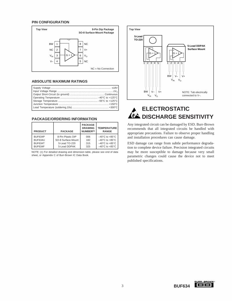
®
BUF6343
PIN CONFIGURATION
Top View 8-Pin Dip PackageSO-8 Surface-Mount Package
Top View
Supply Voltage ..................................................................................... ±18VInput Voltage Range ............................................................................... ±VS
Output Short-Circuit (to ground) .................................................ContinuousOperating Temperature ..................................................... –40°C to +125°CStorage Temperature ........................................................ –55°C to +125°CJunction Temperature ....................................................................... +150°CLead Temperature (soldering,10s) .................................................... +300°C
NC = No Connection
BW
NC
VIN
V–
NC
V+
VO
NC
1
2
3
4
8
7
6
5
G = 1
Any integrated circuit can be damaged by ESD. Burr-Brownrecommends that all integrated circuits be handled withappropriate precautions. Failure to observe proper handlingand installation procedures can cause damage.
ESD damage can range from subtle performance degrada-tion to complete device failure. Precision integrated circuitsmay be more susceptible to damage because very smallparametric changes could cause the device not to meetpublished specifications.
ELECTROSTATICDISCHARGE SENSITIVITY
NOTE: Tab electricallyconnected to V–.
G = 1 G = 1
V–VO
V+VIN
BW
1 2 3 4 5
5-LeadTO-220
V–VO
V+VIN
BW
1 2 3 4 5
5-Lead DDPAKSurface Mount
PACKAGEDRAWING TEMPERATURE
PRODUCT PACKAGE NUMBER (1) RANGE
BUF634P 8-Pin Plastic DIP 006 –40°C to +85°CBUF634U SO-8 Surface-Mount 182 –40°C to +85°CBUF634T 5-Lead TO-220 315 –40°C to +85°CBUF634F 5-Lead DDPAK 325 –40°C to +85°C
NOTE: (1) For detailed drawing and dimension table, please see end of datasheet, or Appendix C of Burr-Brown IC Data Book.
PACKAGE/ORDERING INFORMATION
ABSOLUTE MAXIMUM RATINGS
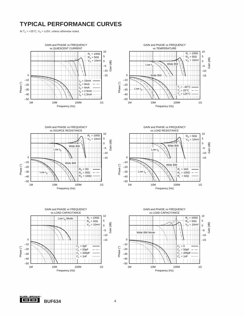
4®
BUF634
GAIN and PHASE vs FREQUENCYvs LOAD CAPACITANCE
Frequency (Hz)1M 10M 100M 1G
Pha
se (
°)
0
–10
–20
–30
–40
–50
CL = 0CL = 50pFCL = 200pFCL = 1nF
10
5
0
–5
–10
–15
Gai
n (d
B)
Wide BW Mode
RL = 100ΩRS = 50ΩVO = 10mV
GAIN and PHASE vs FREQUENCYvs LOAD CAPACITANCE
Frequency (Hz)1M 10M 100M 1G
Pha
se (
°)
0
–10
–20
–30
–40
–50
CL = 0pFCL = 50pFCL = 200pFCL = 1nF
10
5
0
–5
–10
–15
Gai
n (d
B)
Low IQ Mode RL = 100ΩRS = 50ΩVO = 10mV
GAIN and PHASE vs FREQUENCYvs LOAD RESISTANCE
Frequency (Hz)1M 10M 100M 1G
Pha
se (
°)
0
–10
–20
–30
–40
–50
RL = 1kΩRL = 100ΩRL = 50Ω
10
5
0
–5
–10
–15
Gai
n (d
B)
RS = 50ΩVO = 10mV
Wide BW
Low IQ
Low IQ
Wide BW
GAIN and PHASE vs FREQUENCYvs SOURCE RESISTANCE
Frequency (Hz)1M 10M 100M 1G
Pha
se (
°)
0
–10
–20
–30
–40
–50
RS = 0ΩRS = 50ΩRS = 100Ω
10
5
0
–5
–10
–15
Gai
n (d
B)
Wide BWLow IQ
Low IQ
Wide BW
RL = 100ΩVO = 10mV
GAIN and PHASE vs FREQUENCYvs TEMPERATURE
Frequency (Hz)1M 10M 100M 1G
Pha
se (
°)
0
–10
–20
–30
–40
–50
TJ = –40°CTJ = 25°CTJ = 125°C
10
5
0
–5
–10
–15
Gai
n (d
B)
Wide BW
Wide BW
Low IQ
Low IQ
RL = 100ΩRS = 50ΩVO = 10mV
GAIN and PHASE vs FREQUENCYvs QUIESCENT CURRENT
Frequency (Hz)1M 10M 100M 1G
Pha
se (
°)
0
–10
–20
–30
–40
–50
IQ = 15mAIQ = 9mAIQ = 4mAIQ = 2.5mAIQ = 1.5mA
10
5
0
–5
–10
–15
Gai
n (d
B)
RL = 100ΩRS = 50ΩVO = 10mV
TYPICAL PERFORMANCE CURVESAt TA = +25°C, VS = ±15V, unless otherwise noted.
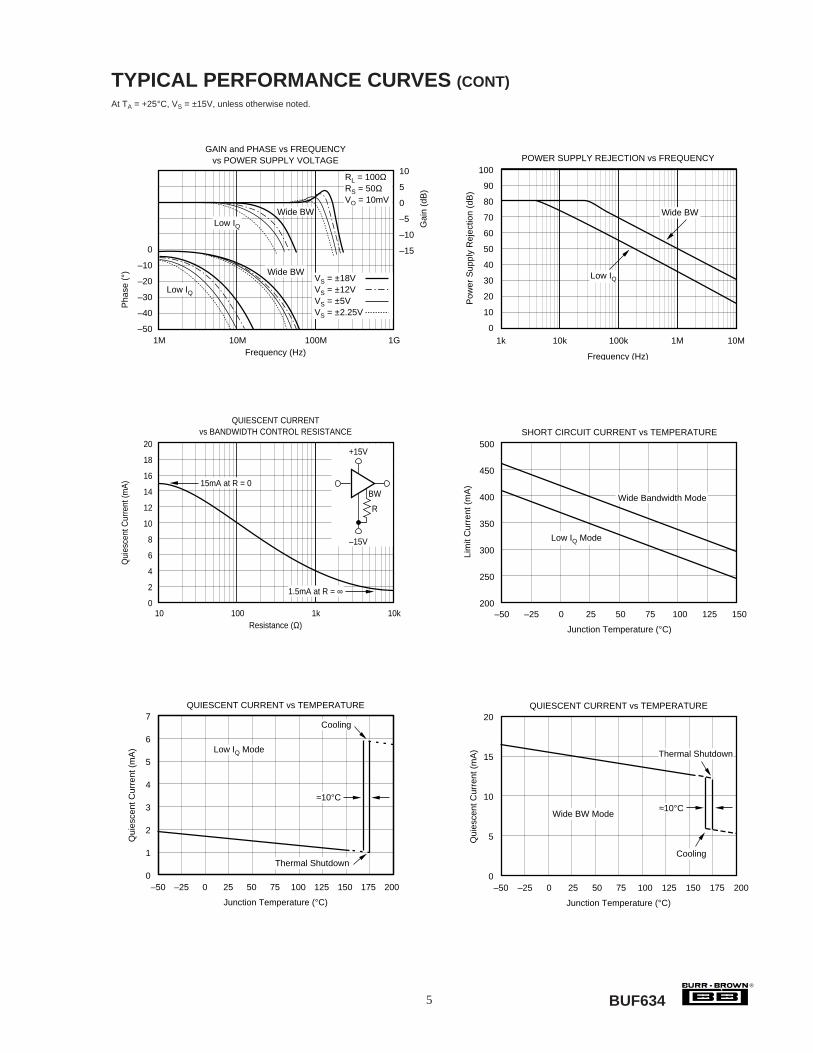
®
BUF6345
QUIESCENT CURRENT vs TEMPERATURE20
15
10
5
0
Junction Temperature (°C)
–50 –25 0 25 50 75 100 125 150 175 200
Thermal Shutdown
≈10°C
Cooling
Wide BW Mode
Qui
esce
nt C
urre
nt (
mA
)
QUIESCENT CURRENT vs TEMPERATURE7
6
5
4
3
2
1
0
Qui
esce
nt C
urre
nt (
mA
)
Junction Temperature (°C)
–50 –25 0 25 50 75 100 125 150 175 200
Cooling
Thermal Shutdown
Low IQ Mode
≈10°C
GAIN and PHASE vs FREQUENCYvs POWER SUPPLY VOLTAGE
Frequency (Hz)1M 10M 100M 1G
Pha
se (
°)
0
–10
–20
–30
–40
–50
VS = ±18VVS = ±12VVS = ±5VVS = ±2.25V
10
5
0
–5
–10
–15
Gai
n (d
B)
Wide BWLow IQ
Low IQ
Wide BW
RL = 100ΩRS = 50ΩVO = 10mV
TYPICAL PERFORMANCE CURVES (CONT)At TA = +25°C, VS = ±15V, unless otherwise noted.
POWER SUPPLY REJECTION vs FREQUENCY100
90
80
70
60
50
40
30
20
10
01k 10k 100k 1M 10M
Frequency (Hz)
Wide BW
Low IQ
Pow
er S
uppl
y R
ejec
tion
(dB
)
SHORT CIRCUIT CURRENT vs TEMPERATURE500
450
400
350
300
250
200–50 –25 0 25 50 75 100 125 150
Junction Temperature (°C)
Wide Bandwidth Mode
Low IQ Mode
Lim
it C
urre
nt (
mA
)
QUIESCENT CURRENTvs BANDWIDTH CONTROL RESISTANCE
Resistance (Ω)10 100 1k 10k
Qui
esce
nt C
urre
nt (m
A)
20
18
16
14
12
10
8
6
4
2
0
15mA at R = 0
1.5mA at R = ∞
R
–15V
+15V
BW
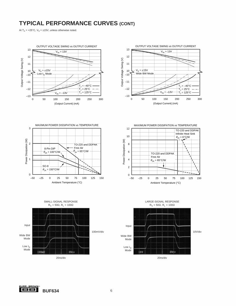
6®
BUF634
OUTPUT VOLTAGE SWING vs OUTPUT CURRENT13
12
11
10
–10
–11
–12
–130 50 100 150 200 250 300
|Output Current| (mA)
TJ = –40°CTJ = 25°CTJ = 125°C
VIN = 13V
VIN = –13V
VS = ±15VLow IQ Mode
Out
put V
olta
ge S
win
g (V
)TYPICAL PERFORMANCE CURVES (CONT)At TA = +25°C, VS = ±15V, unless otherwise noted.
Wide BWMode
Low IQMode
Input
Wide BWMode
Low IQMode
Input
LARGE-SIGNAL RESPONSERS = 50Ω, RL = 100Ω
SMALL-SIGNAL RESPONSERS = 50Ω, RL = 100Ω
20ns/div 20ns/div
100mV/div 10V/div
OUTPUT VOLTAGE SWING vs OUTPUT CURRENT13
12
11
10
–10
–11
–12
–130 50 100 150 200 250 300
|Output Current| (mA)
TJ = –40°CTJ = 25°CTJ = 125°C
VIN = 13V
VIN = –13V
VS = ±15VWide BW Mode
Out
put V
olta
ge S
win
g (V
)MAXIMUM POWER DISSIPATION vs TEMPERATURE
Ambient Temperature (°C)
3
2
1
0–50 –25 0 25 50 75 100 125 150
Pow
er D
issi
patio
n (W
)
TO-220 and DDPAKFree Air
JA = 65°C/Wθ8-Pin DIP
JA = 100°C/Wθ
SO-8
JA = 150°C/Wθ
MAXIMUM POWER DISSIPATION vs TEMPERATURE
Ambient Temperature (°C)
12
10
8
6
4
2
0
Pow
er D
issi
patio
n (W
)
–50 –25 0 25 50 75 100 125 150
TO-220 and DDPAKInfinite Heat Sink
JC = 6°C/Wθ
TO-220 and DDPAKFree Air
JA = 65°C/Wθ
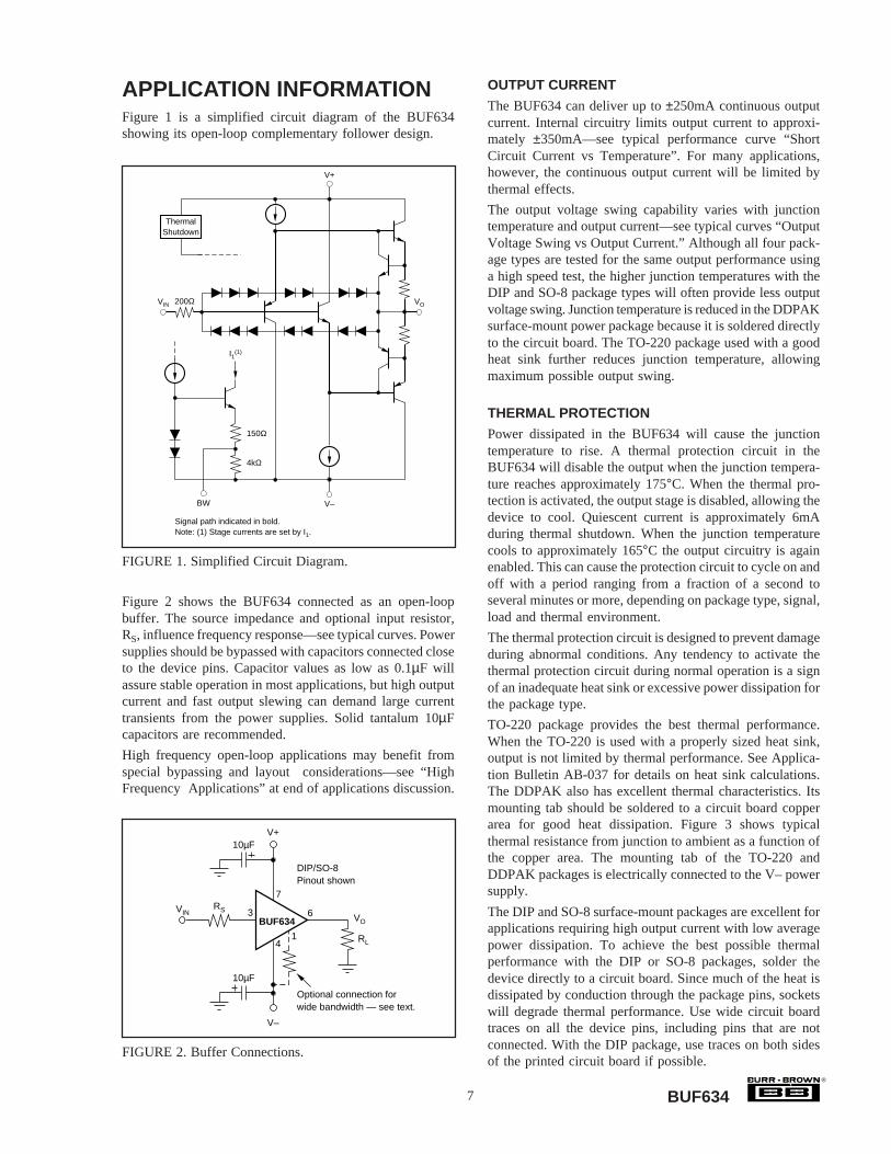
®
BUF6347
APPLICATION INFORMATIONFigure 1 is a simplified circuit diagram of the BUF634showing its open-loop complementary follower design.
FIGURE 2. Buffer Connections.
V–
10µF
10µF
VOBUF634
Optional connection forwide bandwidth — see text.
RS 3
V+
6
RL4
7
1
VIN
DIP/SO-8Pinout shown
OUTPUT CURRENT
The BUF634 can deliver up to ±250mA continuous outputcurrent. Internal circuitry limits output current to approxi-mately ±350mA—see typical performance curve “ShortCircuit Current vs Temperature”. For many applications,however, the continuous output current will be limited bythermal effects.
The output voltage swing capability varies with junctiontemperature and output current—see typical curves “OutputVoltage Swing vs Output Current.” Although all four pack-age types are tested for the same output performance usinga high speed test, the higher junction temperatures with theDIP and SO-8 package types will often provide less outputvoltage swing. Junction temperature is reduced in the DDPAKsurface-mount power package because it is soldered directlyto the circuit board. The TO-220 package used with a goodheat sink further reduces junction temperature, allowingmaximum possible output swing.
THERMAL PROTECTION
Power dissipated in the BUF634 will cause the junctiontemperature to rise. A thermal protection circuit in theBUF634 will disable the output when the junction tempera-ture reaches approximately 175°C. When the thermal pro-tection is activated, the output stage is disabled, allowing thedevice to cool. Quiescent current is approximately 6mAduring thermal shutdown. When the junction temperaturecools to approximately 165°C the output circuitry is againenabled. This can cause the protection circuit to cycle on andoff with a period ranging from a fraction of a second toseveral minutes or more, depending on package type, signal,load and thermal environment.
The thermal protection circuit is designed to prevent damageduring abnormal conditions. Any tendency to activate thethermal protection circuit during normal operation is a signof an inadequate heat sink or excessive power dissipation forthe package type.
TO-220 package provides the best thermal performance.When the TO-220 is used with a properly sized heat sink,output is not limited by thermal performance. See Applica-tion Bulletin AB-037 for details on heat sink calculations.The DDPAK also has excellent thermal characteristics. Itsmounting tab should be soldered to a circuit board copperarea for good heat dissipation. Figure 3 shows typicalthermal resistance from junction to ambient as a function ofthe copper area. The mounting tab of the TO-220 andDDPAK packages is electrically connected to the V– powersupply.
The DIP and SO-8 surface-mount packages are excellent forapplications requiring high output current with low averagepower dissipation. To achieve the best possible thermalperformance with the DIP or SO-8 packages, solder thedevice directly to a circuit board. Since much of the heat isdissipated by conduction through the package pins, socketswill degrade thermal performance. Use wide circuit boardtraces on all the device pins, including pins that are notconnected. With the DIP package, use traces on both sidesof the printed circuit board if possible.
Figure 2 shows the BUF634 connected as an open-loopbuffer. The source impedance and optional input resistor,RS, influence frequency response—see typical curves. Powersupplies should be bypassed with capacitors connected closeto the device pins. Capacitor values as low as 0.1µF willassure stable operation in most applications, but high outputcurrent and fast output slewing can demand large currenttransients from the power supplies. Solid tantalum 10µFcapacitors are recommended.
High frequency open-loop applications may benefit fromspecial bypassing and layout considerations—see “HighFrequency Applications” at end of applications discussion.
FIGURE 1. Simplified Circuit Diagram.
200Ω
I1(1)
V+
VO
BW V–
150Ω
4kΩ
Signal path indicated in bold.Note: (1) Stage currents are set by I1.
ThermalShutdown
VIN
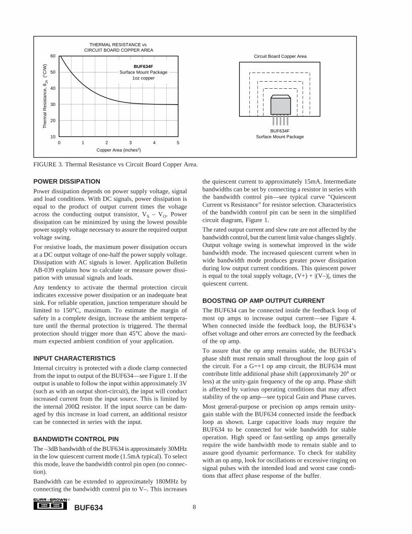
8®
BUF634
the quiescent current to approximately 15mA. Intermediatebandwidths can be set by connecting a resistor in series withthe bandwidth control pin—see typical curve "QuiescentCurrent vs Resistance" for resistor selection. Characteristicsof the bandwidth control pin can be seen in the simplifiedcircuit diagram, Figure 1.
The rated output current and slew rate are not affected by thebandwidth control, but the current limit value changes slightly.Output voltage swing is somewhat improved in the widebandwidth mode. The increased quiescent current when inwide bandwidth mode produces greater power dissipationduring low output current conditions. This quiescent poweris equal to the total supply voltage, (V+) + |(V–)|, times thequiescent current.
BOOSTING OP AMP OUTPUT CURRENT
The BUF634 can be connected inside the feedback loop ofmost op amps to increase output current—see Figure 4.When connected inside the feedback loop, the BUF634’soffset voltage and other errors are corrected by the feedbackof the op amp.
To assure that the op amp remains stable, the BUF634’sphase shift must remain small throughout the loop gain ofthe circuit. For a G=+1 op amp circuit, the BUF634 mustcontribute little additional phase shift (approximately 20° orless) at the unity-gain frequency of the op amp. Phase shiftis affected by various operating conditions that may affectstability of the op amp—see typical Gain and Phase curves.
Most general-purpose or precision op amps remain unity-gain stable with the BUF634 connected inside the feedbackloop as shown. Large capacitive loads may require theBUF634 to be connected for wide bandwidth for stableoperation. High speed or fast-settling op amps generallyrequire the wide bandwidth mode to remain stable and toassure good dynamic performance. To check for stabilitywith an op amp, look for oscillations or excessive ringing onsignal pulses with the intended load and worst case condi-tions that affect phase response of the buffer.
POWER DISSIPATION
Power dissipation depends on power supply voltage, signaland load conditions. With DC signals, power dissipation isequal to the product of output current times the voltageacross the conducting output transistor, VS – VO. Powerdissipation can be minimized by using the lowest possiblepower supply voltage necessary to assure the required outputvoltage swing.
For resistive loads, the maximum power dissipation occursat a DC output voltage of one-half the power supply voltage.Dissipation with AC signals is lower. Application BulletinAB-039 explains how to calculate or measure power dissi-pation with unusual signals and loads.
Any tendency to activate the thermal protection circuitindicates excessive power dissipation or an inadequate heatsink. For reliable operation, junction temperature should belimited to 150°C, maximum. To estimate the margin ofsafety in a complete design, increase the ambient tempera-ture until the thermal protection is triggered. The thermalprotection should trigger more than 45°C above the maxi-mum expected ambient condition of your application.
INPUT CHARACTERISTICS
Internal circuitry is protected with a diode clamp connectedfrom the input to output of the BUF634—see Figure 1. If theoutput is unable to follow the input within approximately 3V(such as with an output short-circuit), the input will conductincreased current from the input source. This is limited bythe internal 200Ω resistor. If the input source can be dam-aged by this increase in load current, an additional resistorcan be connected in series with the input.
BANDWIDTH CONTROL PIN
The –3dB bandwidth of the BUF634 is approximately 30MHzin the low quiescent current mode (1.5mA typical). To selectthis mode, leave the bandwidth control pin open (no connec-tion).
Bandwidth can be extended to approximately 180MHz byconnecting the bandwidth control pin to V–. This increases
FIGURE 3. Thermal Resistance vs Circuit Board Copper Area.
Circuit Board Copper Area
BUF634FSurface Mount Package
THERMAL RESISTANCE vs CIRCUIT BOARD COPPER AREA
60
50
40
30
20
10
The
rmal
Res
ista
nce,
θJA
(°C
/W)
0 1 2 3 4 5
Copper Area (inches2)
BUF634FSurface Mount Package
1oz copper
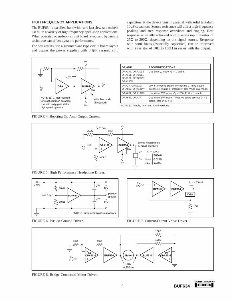
®
BUF6349
HIGH FREQUENCY APPLICATIONS
The BUF634’s excellent bandwidth and fast slew rate make ituseful in a variety of high frequency open-loop applications.When operated open-loop, circuit board layout and bypassingtechnique can affect dynamic performance.
For best results, use a ground plane type circuit board layoutand bypass the power supplies with 0.1µF ceramic chip
capacitors at the device pins in parallel with solid tantalum10µF capacitors. Source resistance will affect high-frequencypeaking and step response overshoot and ringing. Bestresponse is usually achieved with a series input resistor of25Ω to 200Ω, depending on the signal source. Responsewith some loads (especially capacitive) can be improvedwith a resistor of 10Ω to 150Ω in series with the output.
OP AMP RECOMMENDATIONS
OPA177, OPA1013 Use Low IQ mode. G = 1 stable.OPA111, OPA2111OPA121, OPA234(1),OPA130(1)
OPA27, OPA2107 Low IQ mode is stable. Increasing CL may causeOPA602, OPA131(1) excessive ringing or instability. Use Wide BW mode.
OPA627, OPA132(1) Use Wide BW mode, C1 = 200pF. G = 1 stable.
OPA637, OPA37 Use Wide BW mode. These op amps are not G = 1stable. Use in G > 4.
NOTE: (1) Single, dual, and quad versions.
OPA
NOTE: (1) C1 not requiredfor most common op amps.Use with unity-gain stablehigh speed op amps.
VIN
VO
V+
V–
BUF634
C1(1)
Wide BW mode(if required)
BW
FIGURE 5. High Performance Headphone Driver.
FIGURE 8. Bridge-Connected Motor Driver.
1/2OPA2234
9kΩ
BUF634
1kΩ
VIN±1V
Motor 1/2
OPA2234BUF634
10kΩ
10kΩ
±20Vat 250mA
FIGURE 7. Current-Output Valve Driver.
OPA177 BUF634
Valve
VIN±2V
10Ω
IO = ±200mA
FIGURE 4. Boosting Op Amp Output Current.
C(1)
C(1)
pseudoground
+12V
–
BUF634
10kΩ
10µF
+24V10kΩ
+12V
–
NOTE: (1) System bypass capacitors.
+
FIGURE 6. Pseudo-Ground Driver.
OPA132Drives headphonesor small speakers.
5kΩ
BUF634
100kΩ
1µF
RL = 100Ωf
1kHz
20kHz
THD+N
0.015%
0.02%
250ΩG = +21
VIN
V–
BW
V+

IMPORTANT NOTICE
Texas Instruments and its subsidiaries (TI) reserve the right to make changes to their products or to discontinueany product or service without notice, and advise customers to obtain the latest version of relevant informationto verify, before placing orders, that information being relied on is current and complete. All products are soldsubject to the terms and conditions of sale supplied at the time of order acknowledgment, including thosepertaining to warranty, patent infringement, and limitation of liability.
TI warrants performance of its semiconductor products to the specifications applicable at the time of sale inaccordance with TI’s standard warranty. Testing and other quality control techniques are utilized to the extentTI deems necessary to support this warranty. Specific testing of all parameters of each device is not necessarilyperformed, except those mandated by government requirements.
Customers are responsible for their applications using TI components.
In order to minimize risks associated with the customer’s applications, adequate design and operatingsafeguards must be provided by the customer to minimize inherent or procedural hazards.
TI assumes no liability for applications assistance or customer product design. TI does not warrant or representthat any license, either express or implied, is granted under any patent right, copyright, mask work right, or otherintellectual property right of TI covering or relating to any combination, machine, or process in which suchsemiconductor products or services might be or are used. TI’s publication of information regarding any thirdparty’s products or services does not constitute TI’s approval, warranty or endorsement thereof.
Copyright 2000, Texas Instruments Incorporated

This datasheet has been download from:
www.datasheetcatalog.com
Datasheets for electronics components.
Mar-10-20041
BAV199...
Silicon Low Leakage Diode• Low-leakage applications
• Medium speed switching times
• Series pair configuration
BAV199BAV199F
Type Package Configuration MarkingBAV199 BAV199F*
SOT23 TSFP-3
series series
JYs JYs
* Preliminary
Maximum Ratings at TA = 25°C, unless otherwise specifiedParameter Symbol Value UnitDiode reverse voltage VR 80 V
Peak reverse voltage VRM 85
Forward current IF 200 mA
Non-repetitive peak surge forward current t = 1 µs t = 1 s
IFSM 4.50.5
A
Total power dissipation BAV199, TS ≤ 31°C BAV199F, TS ≤ tbd
Ptot 330250
mW
Junction temperature T j 150 °C
Storage temperature Tstg -65 ... 150
Mar-10-20042
BAV199...
Thermal ResistanceParameter Symbol Value UnitJunction - soldering point1) BAV199 BAV199F
RthJS ≤ 360 ≤ tbd
K/W
Electrical Characteristics at TA = 25°C, unless otherwise specifiedParameter Symbol Values Unit
min. typ. max.DC CharacteristicsBreakdown voltage I(BR) = 100 µA
V(BR) 85 - - V
Reverse current VR = 75 V VR = 75 V, TA = 150 °C
IR --
--
5
80
nA
Forward voltage IF = 1 mA IF = 10 mA IF = 50 mA IF = 150 mA
VF ----
----
900
100011001250
mV
AC CharacteristicsDiode capacitance VR = 0 V, f = 1 MHz
CT - 2 - pF
Reverse recovery time IF = 10 mA, IR = 10 mA, measured at IR = 1mA , RL = 100 Ω
trr - 0.6 1.5 µs
Test circuit for reverse recovery time
EHN00019
Ι F
D.U.T.
Oscillograph
Pulse generator: tp = 10µs, D = 0.05, tr = 0.6ns, Ri = 50Ω
Oscillograph: R = 50Ω, tr = 0.35ns, C ≤ 1pF
1For calculation of RthJA please refer to Application Note Thermal Resistance
Mar-10-20043
BAV199...
Reverse current IR = ƒ (TA)VR = 70V
0 50 100 150
BAV 199 EHB00085
nA
TA
˚C
max
typ
10 2
10 1
010
-110
-310
Ι R
-210
Forward Voltage VF = ƒ (TA)IF = Parameter
0
0.5
1.0
1.5
0 50 100 150
BAV 199 EHB00088
V
TA
VF
˚C
150 mA
50 mA
10 mA
1 mA
0.1 mA
Ι F =
Forward current IF = ƒ (VF)TA = 25°C
00
EHB00086BAV 199
Ι
0.5 1.0 V 1.5
50
100
mA
150
F
FV
maxtyp
Forward current IF = ƒ (TS)BAV199
0 15 30 45 60 75 90 105 120 °C 150
TS
0
25
50
75
100
125
150
175
200
mA
250
IF
Mar-10-20044
BAV199...
Permissible Puls Load RthJS = ƒ (tp)
10 -7 10 -6 10 -5 10 -4 10 -3 10 -2 10 0 s
TP
-1 10
0 10
1 10
2 10
3 10
Rth
JS
D = 0,50,20,10,050,020,010,0050
Permissible Pulse LoadIFmax/ IFDC = ƒ (tp)
10 -6 10 -5 10 -4 10 -3 10 -2 10 0 s
TP
0 10
1 10
2 10
-
I Fm
ax/I F
DC
D = 00.0050.010.020.050.10.20.5

This datasheet has been download from:
www.datasheetcatalog.com
Datasheets for electronics components.
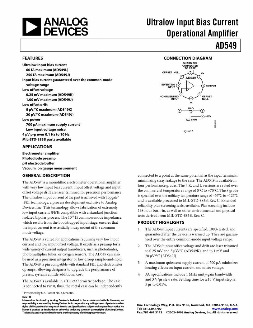
Ultralow Input Bias CurrentOperational Amplifier
AD549
Rev. H Information furnished by Analog Devices is believed to be accurate and reliable. However, no responsibility is assumed by Analog Devices for its use, nor for any infringements of patents or other rights of third parties that may result from its use. Specifications subject to change without notice. No license is granted by implication or otherwise under any patent or patent rights of Analog Devices. Trademarks and registered trademarks are the property of their respective owners.
One Technology Way, P.O. Box 9106, Norwood, MA 02062-9106, U.S.A.Tel: 781.329.4700 www.analog.com Fax: 781.461.3113 ©2002–2008 Analog Devices, Inc. All rights reserved.
FEATURES Ultralow input bias current
60 fA maximum (AD549L) 250 fA maximum (AD549J)
Input bias current guaranteed over the common-mode voltage range
Low offset voltage 0.25 mV maximum (AD549K) 1.00 mV maximum (AD549J)
Low offset drift 5 μV/°C maximum (AD549K) 20 μV/°C maximum (AD549J)
Low power 700 μA maximum supply current Low input voltage noise
4 μV p-p over 0.1 Hz to 10 Hz MIL-STD-883B parts available
APPLICATIONS Electrometer amplifier Photodiode preamp pH electrode buffer Vacuum ion gauge measurement
CONNECTION DIAGRAM
0051
1-00
1
AD549
OFFSET NULL
OUTPUT
V–
OFFSETNULL
NONINVERTINGINPUT
V+
GUARD PIN,CONNECTED
TO CASE
INVERTINGINPUT
VOS TRIM–15V
10kΩ
6
1
5
4
7
3
2
8
1 5
4
Figure 1.
GENERAL DESCRIPTION The AD5491 is a monolithic electrometer operational amplifier with very low input bias current. Input offset voltage and input offset voltage drift are laser trimmed for precision performance. The ultralow input current of the part is achieved with Topgate™ JFET technology, a process development exclusive to Analog Devices, Inc. This technology allows fabrication of extremely low input current JFETs compatible with a standard junction isolated bipolar process. The 1015 Ω common-mode impedance, which results from the bootstrapped input stage, ensures that the input current is essentially independent of the common-mode voltage.
The AD549 is suited for applications requiring very low input current and low input offset voltage. It excels as a preamp for a wide variety of current output transducers, such as photodiodes, photomultiplier tubes, or oxygen sensors. The AD549 can also be used as a precision integrator or low droop sample-and-hold. The AD549 is pin compatible with standard FET and electrometer op amps, allowing designers to upgrade the performance of present systems at little additional cost.
The AD549 is available in a TO-99 hermetic package. The case is connected to Pin 8, thus, the metal case can be independently
connected to a point at the same potential as the input terminals, minimizing stray leakage to the case. The AD549 is available in four performance grades. The J, K, and L versions are rated over the commercial temperature range of 0°C to +70°C. The S grade is specified over the military temperature range of −55°C to +125°C and is available processed to MIL-STD-883B, Rev. C. Extended reliability plus screening is also available. Plus screening includes 168 hour burn-in, as well as other environmental and physical tests derived from MIL-STD-883B, Rev. C.
PRODUCT HIGHLIGHTS 1. The AD549 input currents are specified, 100% tested, and
guaranteed after the device is warmed up. They are guaran-teed over the entire common-mode input voltage range.
2. The AD549 input offset voltage and drift are laser trimmed to 0.25 mV and 5 μV/°C (AD549K), and to 1 mV and 20 μV/°C (AD549J).
3. A maximum quiescent supply current of 700 μA minimizes heating effects on input current and offset voltage.
4. AC specifications include 1 MHz unity-gain bandwidth and 3 V/μs slew rate. Settling time for a 10 V input step is 5 μs to 0.01%.
1 Protected by U.S. Patent No. 4,639,683.
AD549
Rev. H | Page 2 of 20
TABLE OF CONTENTS Features .............................................................................................. 1
Applications ....................................................................................... 1
Connection Diagram ....................................................................... 1
General Description ......................................................................... 1
Product Highlights ........................................................................... 1
Revision History ............................................................................... 2
Specifications ..................................................................................... 3
Absolute Maximum Ratings ............................................................ 5
ESD Caution .................................................................................. 5
Typical Performance Characteristics ............................................. 6
Functional Description .................................................................. 10
Minimizing Input Current ........................................................ 10
Circuit Board Notes ................................................................... 10
Offset Nulling ............................................................................. 11
AC Response with High Value Source and Feedback Resistance .................................................................................... 12
Common-Mode Input Voltage Overload ............................... 12
Differential Input Voltage Overload ........................................ 13
Input Protection ......................................................................... 13
Sample and Difference Circuit to Measure Electrometer Leakage Currents ........................................................................ 13
Photodiode Interface ................................................................. 14
Log Ratio Amplifier ................................................................... 15
Temperature Compensated pH Probe Amplifier ................... 16
Outline Dimensions ....................................................................... 18
Ordering Guide .......................................................................... 18
REVISION HISTORY 3/08—Rev. G to Rev. H Changes to Features .......................................................................... 1 Changes to Figure 1 .......................................................................... 1 Deleted Package Option Parameter ............................................... 4 Inserted ESD Caution ...................................................................... 5 Changes to Figure 2, Figure 3, and Figure 7.................................. 6 Changes to Figure 11 ........................................................................ 7 Changes to Figure 17 ........................................................................ 8 Changes to Figure 41 ...................................................................... 14
7/07—Rev. F to Rev. G Changes to Figure 45 ...................................................................... 16 Changes to Temperature Compensated pH Probe Amplifier Section ............................................................................ 17 Changes to Figure 46 ...................................................................... 17 Changes to Ordering Guide .......................................................... 18
5/06—Rev. E to Rev. F Removed ESD Caution ..................................................................... 5
8/05—Rev. D to Rev. E Change to Figure 22 .......................................................................... 9
5/04—Rev. C to Rev. D Updated Format .................................................................. Universal Changes to Features .......................................................................... 1 Updated Outline Dimensions ....................................................... 18 Added Ordering Guide .................................................................. 18
10/02—Rev. B to Rev. C Deleted Product Highlights #5 ........................................................ 1 Edits to Specifications ....................................................................... 3 Deleted Metallization Photograph .................................................. 3 Updated Outline Dimensions ....................................................... 13
7/02—Rev. A to Rev. B Edits to Specifications ....................................................................... 2
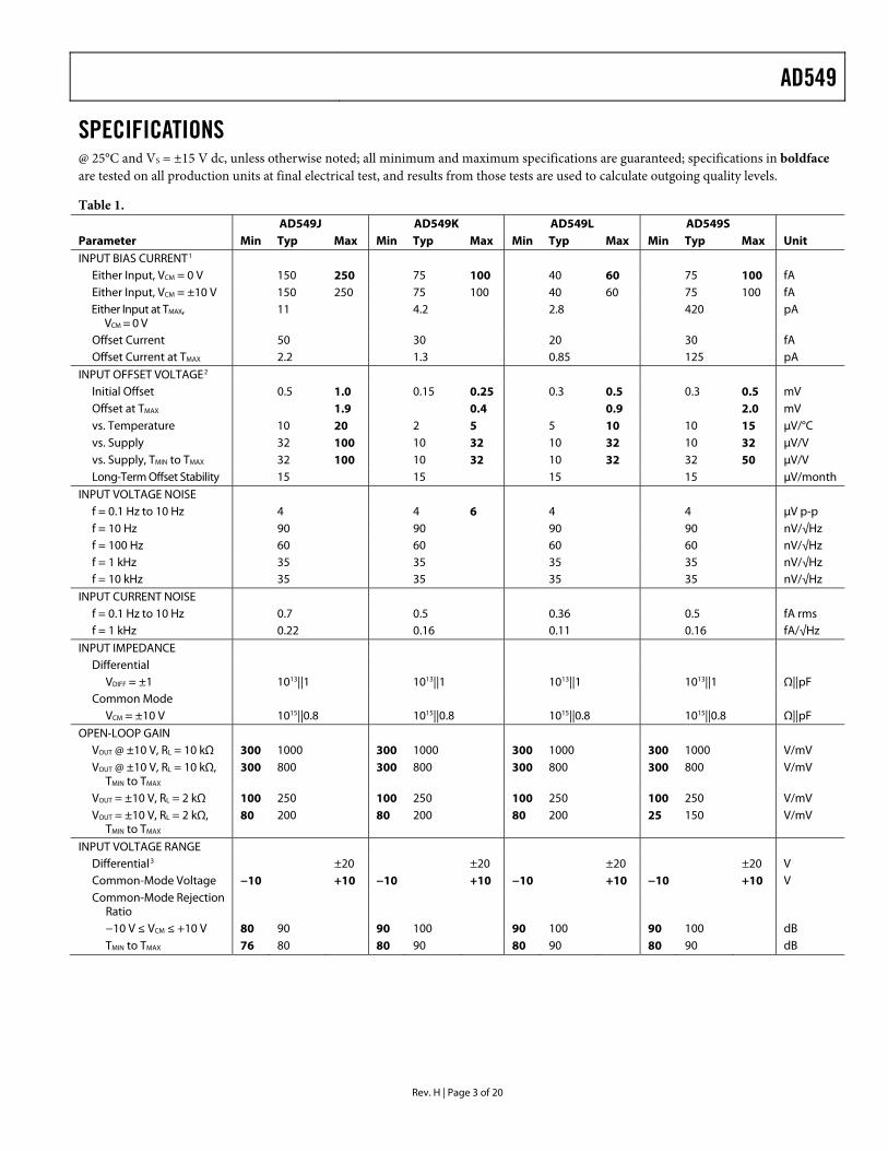
AD549
Rev. H | Page 3 of 20
SPECIFICATIONS @ 25°C and VS = ±15 V dc, unless otherwise noted; all minimum and maximum specifications are guaranteed; specifications in boldface are tested on all production units at final electrical test, and results from those tests are used to calculate outgoing quality levels.
Table 1. AD549J AD549K AD549L AD549S Parameter Min Typ Max Min Typ Max Min Typ Max Min Typ Max Unit INPUT BIAS CURRENT1
Either Input, VCM = 0 V 150 250 75 100 40 60 75 100 fA Either Input, VCM = ±10 V 150 250 75 100 40 60 75 100 fA Either Input at TMAX,
VCM = 0 V 11 4.2 2.8 420 pA
Offset Current 50 30 20 30 fA Offset Current at TMAX 2.2 1.3 0.85 125 pA
INPUT OFFSET VOLTAGE2
Initial Offset 0.5 1.0 0.15 0.25 0.3 0.5 0.3 0.5 mV Offset at TMAX 1.9 0.4 0.9 2.0 mV vs. Temperature 10 20 2 5 5 10 10 15 μV/°C vs. Supply 32 100 10 32 10 32 10 32 μV/V vs. Supply, TMIN to TMAX 32 100 10 32 10 32 32 50 μV/V Long-Term Offset Stability 15 15 15 15 μV/month
INPUT VOLTAGE NOISE f = 0.1 Hz to 10 Hz 4 4 6 4 4 μV p-p f = 10 Hz 90 90 90 90 nV/√Hz f = 100 Hz 60 60 60 60 nV/√Hz f = 1 kHz 35 35 35 35 nV/√Hz f = 10 kHz 35 35 35 35 nV/√Hz
INPUT CURRENT NOISE f = 0.1 Hz to 10 Hz 0.7 0.5 0.36 0.5 fA rms f = 1 kHz 0.22 0.16 0.11 0.16 fA/√Hz
INPUT IMPEDANCE Differential
VDIFF = ±1 1013||1 1013||1 1013||1 1013||1 Ω||pF Common Mode
VCM = ±10 V 1015||0.8 1015||0.8 1015||0.8 1015||0.8 Ω||pF
OPEN-LOOP GAIN VOUT @ ±10 V, RL = 10 kΩ 300 1000 300 1000 300 1000 300 1000 V/mV VOUT @ ±10 V, RL = 10 kΩ,
TMIN to TMAX 300 800 300 800 300 800 300 800 V/mV
VOUT = ±10 V, RL = 2 kΩ 100 250 100 250 100 250 100 250 V/mV VOUT = ±10 V, RL = 2 kΩ,
TMIN to TMAX 80 200 80 200 80 200 25 150 V/mV
INPUT VOLTAGE RANGE Differential3
±20 ±20 ±20 ±20 V Common-Mode Voltage −10 +10 −10 +10 −10 +10 −10 +10 V Common-Mode Rejection
Ratio
−10 V ≤ VCM ≤ +10 V 80 90 90 100 90 100 90 100 dB TMIN to TMAX 76 80 80 90 80 90 80 90 dB
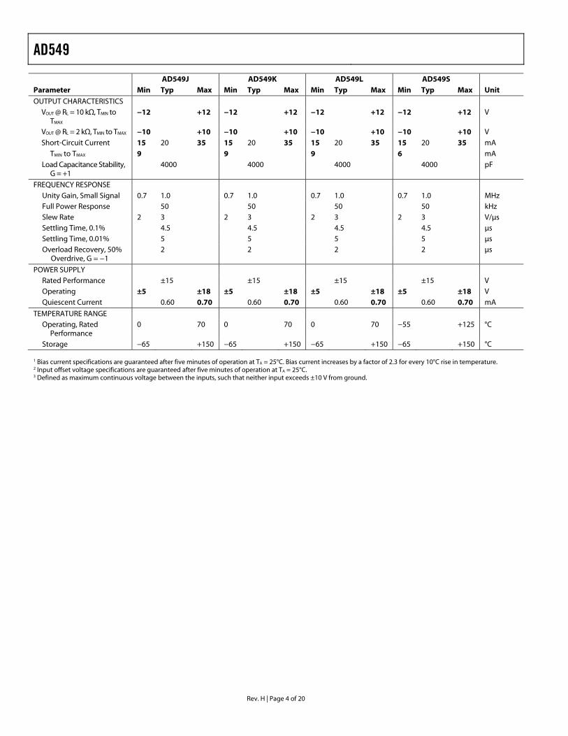
AD549
Rev. H | Page 4 of 20
AD549J AD549K AD549L AD549S Parameter Min Typ Max Min Typ Max Min Typ Max Min Typ Max Unit OUTPUT CHARACTERISTICS
VOUT @ RL = 10 kΩ, TMIN to TMAX
−12 +12 −12 +12 −12 +12 −12 +12 V
VOUT @ RL = 2 kΩ, TMIN to TMAX −10 +10 −10 +10 −10 +10 −10 +10 V Short-Circuit Current 15 20 35 15 20 35 15 20 35 15 20 35 mA
TMIN to TMAX 9 9 9 6 mA Load Capacitance Stability,
G = +1 4000 4000 4000 4000 pF
FREQUENCY RESPONSE Unity Gain, Small Signal 0.7 1.0 0.7 1.0 0.7 1.0 0.7 1.0 MHz Full Power Response 50 50 50 50 kHz Slew Rate 2 3 2 3 2 3 2 3 V/μs Settling Time, 0.1% 4.5 4.5 4.5 4.5 μs Settling Time, 0.01% 5 5 5 5 μs Overload Recovery, 50%
Overdrive, G = −1 2 2 2 2 μs
POWER SUPPLY Rated Performance ±15 ±15 ±15 ±15 V Operating ±5 ±18 ±5 ±18 ±5 ±18 ±5 ±18 V Quiescent Current 0.60 0.70 0.60 0.70 0.60 0.70 0.60 0.70 mA
TEMPERATURE RANGE Operating, Rated
Performance 0 70 0 70 0 70 −55 +125 °C
Storage −65 +150 −65 +150 −65 +150 −65 +150 °C 1 Bias current specifications are guaranteed after five minutes of operation at TA = 25°C. Bias current increases by a factor of 2.3 for every 10°C rise in temperature. 2 Input offset voltage specifications are guaranteed after five minutes of operation at TA = 25°C. 3 Defined as maximum continuous voltage between the inputs, such that neither input exceeds ±10 V from ground.
AD549
Rev. H | Page 5 of 20
ABSOLUTE MAXIMUM RATINGS Table 2. Parameter Rating Supply Voltage ±18 V Internal Power Dissipation 500 mW Input Voltage1
±18 V Output Short-Circuit Duration Indefinite Differential Input Voltage +VS and −VS Storage Temperature Range −65°C to +125°C Operating Temperature Range
AD549J, AD549K, AD549L 0°C to +70°C AD549S −55°C to +125°C
Lead Temperature (Soldering, 60 sec) 300°C 1 For supply voltages less than ±18 V, the absolute maximum input voltage is
equal to the supply voltage.
Stresses above those listed under Absolute Maximum Ratings may cause permanent damage to the device. This is a stress rating only; functional operation of the device at these or any other conditions above those indicated in the operational section of this specification is not implied. Exposure to absolute maximum rating conditions for extended periods may affect device reliability.
ESD CAUTION
AD549
Rev. H | Page 6 of 20
TYPICAL PERFORMANCE CHARACTERISTICS 20
15
10
5
00 5 10 15 20
VIN+
VIN–
0051
1-00
2SUPPLY VOLTAGE (±V)
INPU
T VO
LTA
GE
(V)
Figure 2. Input Voltage Range vs. Supply Voltage
20
15
10
5
00 5 10 15 20
+VOUT
25°CRL = 10kΩ
–VOUT
0051
1-00
3
SUPPLY VOLTAGE (±V)
OU
TPU
T VO
LTA
GE
SWIN
G (V
)
Figure 3. Output Voltage Swing vs. Supply Voltage
30
25
20
15
10
5
010 100 1k 10k 100k
0051
1-00
4
LOAD RESISTANCE (Ω)
OU
TPU
T VO
LTA
GE
SWIN
G (V
p-p
)
VS = ±15V
Figure 4. Output Voltage Swing vs. Load Resistance
800
700
600
500
4000 5 10 15 20
0051
1-00
5
SUPPLY VOLTAGE (±V)
AM
PLIF
IER
QU
IESC
ENT
CU
RR
ENT
(µA
)
Figure 5. Quiescent Current vs. Supply Voltage
120
100
110
90
80
70–20 –10 0 10 20
0051
1-00
6
INPUT COMMON-MODE VOLTAGE (V)
CO
MM
ON
-MO
DE
REJ
ECTI
ON
RA
TIO
(dB
)
Figure 6. CMRR vs. Input Common-Mode Voltage
3000
1000
300
1000 5 10 15 20
0051
1-00
7
SUPPLY VOLTAGE (±V)
OPE
N-L
OO
P G
AIN
(V/m
V)
Figure 7. Open-Loop Gain vs. Supply Voltage
AD549
Rev. H | Page 7 of 20
3000
1000
300
100–55 –25 5 35 65 95 125
0051
1-00
8
TEMPERATURE (°C)
OPE
N-L
OO
P G
AIN
(V/m
V)
Figure 8. Open-Loop Gain vs. Temperature
30
25
20
15
10
5
00 1 2 3 4 5 6 7
0051
1-00
9
WARM-UP TIME (Minutes)
ΔIV
OSI
(µV)
Figure 9. Change in Offset Voltage vs. Warm-Up Time
50
45
40
35
30
25
20–10 –5 0 5 10
0051
1-01
0
COMMON-MODE VOLTAGE (V)
INPU
T C
UR
REN
T (fA
)
Figure 10. Input Bias Current vs. Common-Mode Voltage
50
45
40
35
30
25
200 5 10 15 20
0051
1-01
1
POWER SUPPLY VOLTAGE (±V)
INPU
T C
UR
REN
T (fA
)
Figure 11. Input Bias Current vs. Power Supply Voltage
160
140
120
100
80
60
40
2010 100 1k 10k
0051
1-01
2
FREQUENCY (Hz)
NO
ISE
SPEC
TRA
L D
ENSI
TY (n
V/ H
z)
Figure 12. Input Voltage Noise Spectral Density
100k
10k
1k
100
10
1
0.1100k 1M 10M 100M 1G 10G 100G
0051
1-01
3
SOURCE RESISTANCE (Ω)
INPU
T N
OIS
E VO
LTA
GE
(µV
p-p)
WHENEVER JOHNSON NOISE IS GREATER THANAMPLIFIER NOISE, AMPLIFIER NOISE CAN BECONSIDERED NEGLIGIBLE FOR THE APPLICATION
RESISTORJOHNSON NOISE
10Hz BANDWIDTH
AMPLIFIER GENERATED NOISE
1kHz BANDWIDTH
Figure 13. Noise vs. Source Resistance
AD549
Rev. H | Page 8 of 20
100
80
60
40
20
0
–20
–40
100
–40
–20
0
20
40
60
80
10 100 1k 10k 100k 1M 10M
0051
1-01
4
FREQUENCY (Hz)
OEP
N-L
OO
P G
AIN
(dB
)
PHA
SE M
AR
GIN
(Deg
rees
)Figure 14. Open-Loop Frequency Response
40
35
30
25
20
15
10
5
010 100 1k 10k 100k 1M
0051
1-01
5
FREQUENCY (Hz)
OU
TPU
T VO
LTA
GE
SWIN
G (V
)
Figure 15. Large Signal Frequency Response
100
80
60
40
20
0
–2010 100 1k 10k 100k 10M1M
0051
1-01
6
FREQUENCY (Hz)
CO
MM
ON
-MO
DE
REJ
ECTI
ON
RA
TIO
(dB
)
Figure 16. CMRR vs. Frequency
120
100
80
60
40
20
0
–2010 100 1k 10k 100k 10M1M
0051
1-01
7
FREQUENCY (Hz)
POW
ER S
UPP
LY R
EJEC
TIO
N R
ATI
O (d
B)
+PSSR
–PSSR
Figure 17. PSRR vs. Frequency Response
10
–10
–5
0
5
0 1 32 4
0051
1-01
8
SETTLING TIME (µs)
OU
TPU
T VO
LTA
GE
SWIN
G (V
)
5
10mV
5mV
1mV
10mV
5mV
1mV
Figure 18. Output Voltage Swing and Error vs. Settling Time
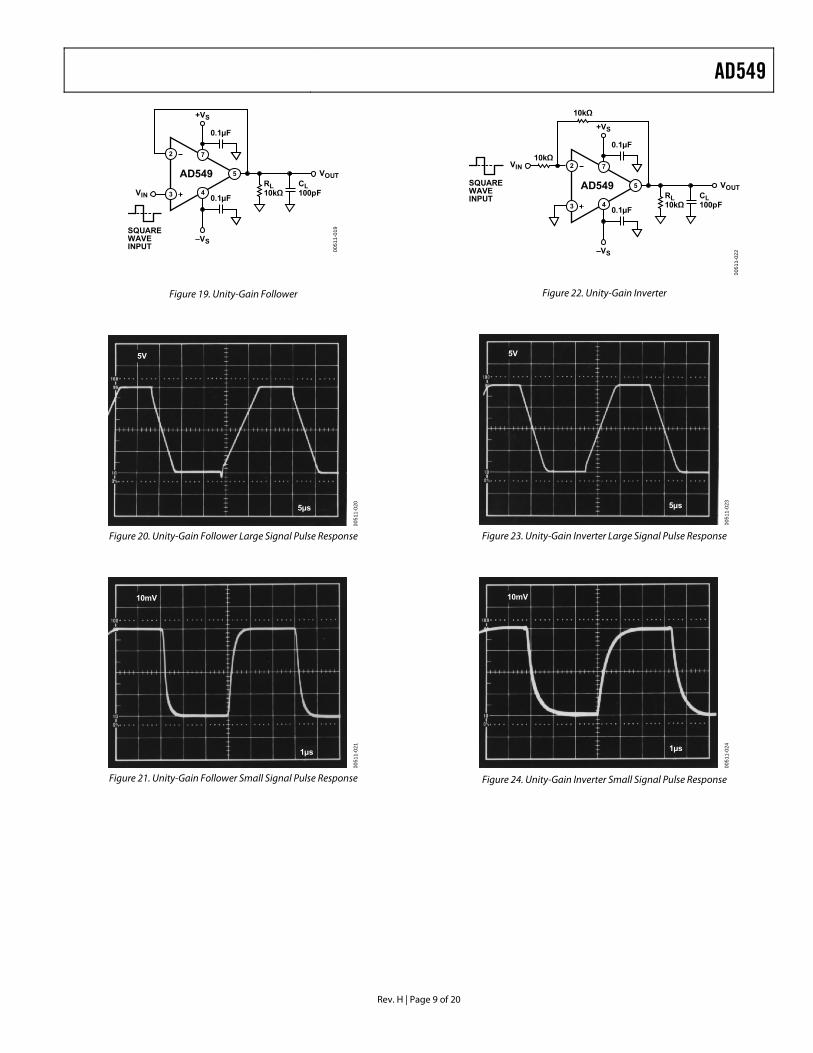
AD549
Rev. H | Page 9 of 20
0051
1-01
9
2
3
5
7
4
AD549RL10kΩ
CL100pF
0.1µF
0.1µFVIN
–VS
+VS
VOUT
SQUAREWAVEINPUT
Figure 19. Unity-Gain Follower
0051
1-02
05V
5µs
Figure 20. Unity-Gain Follower Large Signal Pulse Response
0051
1-02
1
10mV
1µs
Figure 21. Unity-Gain Follower Small Signal Pulse Response
0051
1-02
2
2
3
5
7
4
AD549RL10kΩ
CL100pF
0.1µF
0.1µF
VIN
–VS
+VS
VOUTSQUAREWAVEINPUT
10kΩ
10kΩ
Figure 22. Unity-Gain Inverter
0051
1-02
3
5V
5µs
Figure 23. Unity-Gain Inverter Large Signal Pulse Response
0051
1-02
4
10mV
1µs
Figure 24. Unity-Gain Inverter Small Signal Pulse Response
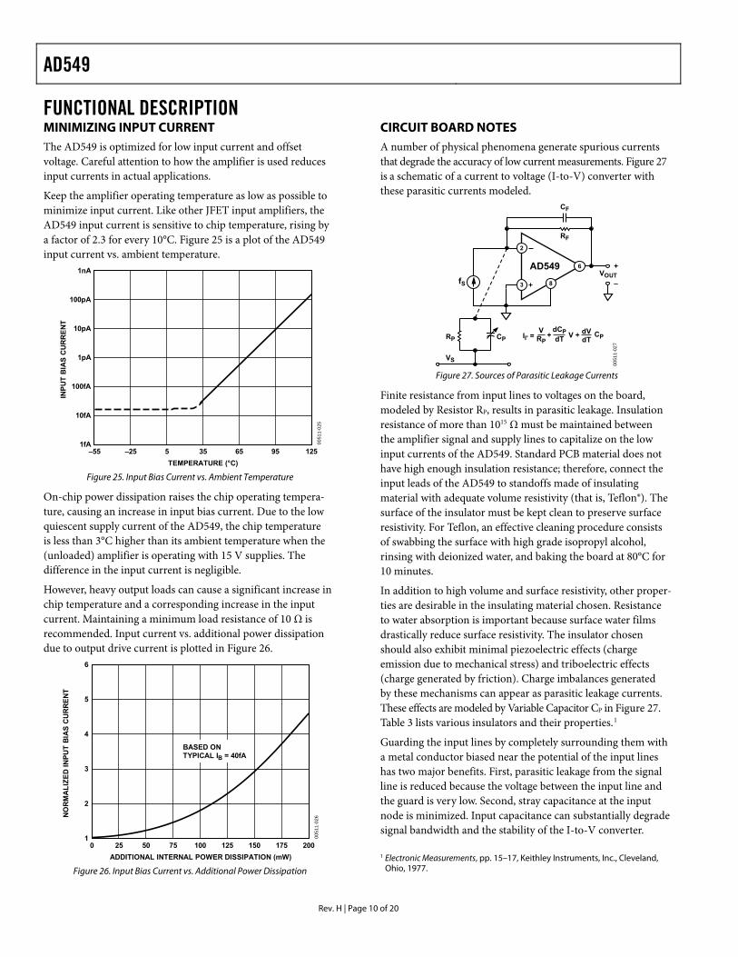
AD549
Rev. H | Page 10 of 20
FUNCTIONAL DESCRIPTION MINIMIZING INPUT CURRENT The AD549 is optimized for low input current and offset voltage. Careful attention to how the amplifier is used reduces input currents in actual applications.
Keep the amplifier operating temperature as low as possible to minimize input current. Like other JFET input amplifiers, the AD549 input current is sensitive to chip temperature, rising by a factor of 2.3 for every 10°C. Figure 25 is a plot of the AD549 input current vs. ambient temperature.
1nA
100pA
10pA
1pA
100fA
10fA
1fA–55 –25 5 35 65 12595
0051
1-02
5
TEMPERATURE (°C)
INPU
T B
IAS
CU
RR
ENT
Figure 25. Input Bias Current vs. Ambient Temperature
On-chip power dissipation raises the chip operating tempera-ture, causing an increase in input bias current. Due to the low quiescent supply current of the AD549, the chip temperature is less than 3°C higher than its ambient temperature when the (unloaded) amplifier is operating with 15 V supplies. The difference in the input current is negligible.
However, heavy output loads can cause a significant increase in chip temperature and a corresponding increase in the input current. Maintaining a minimum load resistance of 10 Ω is recommended. Input current vs. additional power dissipation due to output drive current is plotted in Figure 26.
6
5
4
3
2
10 25 50 75 100 125 150 175 200
0051
1-02
6
ADDITIONAL INTERNAL POWER DISSIPATION (mW)
NO
RM
ALI
ZED
INPU
T B
IAS
CU
RR
ENT
BASED ONTYPICAL IB = 40fA
Figure 26. Input Bias Current vs. Additional Power Dissipation
CIRCUIT BOARD NOTES A number of physical phenomena generate spurious currents that degrade the accuracy of low current measurements. Figure 27 is a schematic of a current to voltage (I-to-V) converter with these parasitic currents modeled.
0051
1-02
7
2
3
6
8
AD549 +VOUT
–fS
CF
RF
VS
RP CP II' = + V + CPV
RP
dCPdT
dVdT
Figure 27. Sources of Parasitic Leakage Currents
Finite resistance from input lines to voltages on the board, modeled by Resistor RP, results in parasitic leakage. Insulation resistance of more than 1015 Ω must be maintained between the amplifier signal and supply lines to capitalize on the low input currents of the AD549. Standard PCB material does not have high enough insulation resistance; therefore, connect the input leads of the AD549 to standoffs made of insulating material with adequate volume resistivity (that is, Teflon®). The surface of the insulator must be kept clean to preserve surface resistivity. For Teflon, an effective cleaning procedure consists of swabbing the surface with high grade isopropyl alcohol, rinsing with deionized water, and baking the board at 80°C for 10 minutes.
In addition to high volume and surface resistivity, other proper-ties are desirable in the insulating material chosen. Resistance to water absorption is important because surface water films drastically reduce surface resistivity. The insulator chosen should also exhibit minimal piezoelectric effects (charge emission due to mechanical stress) and triboelectric effects (charge generated by friction). Charge imbalances generated by these mechanisms can appear as parasitic leakage currents. These effects are modeled by Variable Capacitor CP in Figure 27. Table 3 lists various insulators and their properties.1
Guarding the input lines by completely surrounding them with a metal conductor biased near the potential of the input lines has two major benefits. First, parasitic leakage from the signal line is reduced because the voltage between the input line and the guard is very low. Second, stray capacitance at the input node is minimized. Input capacitance can substantially degrade signal bandwidth and the stability of the I-to-V converter. 1 Electronic Measurements, pp. 15–17, Keithley Instruments, Inc., Cleveland,
Ohio, 1977.
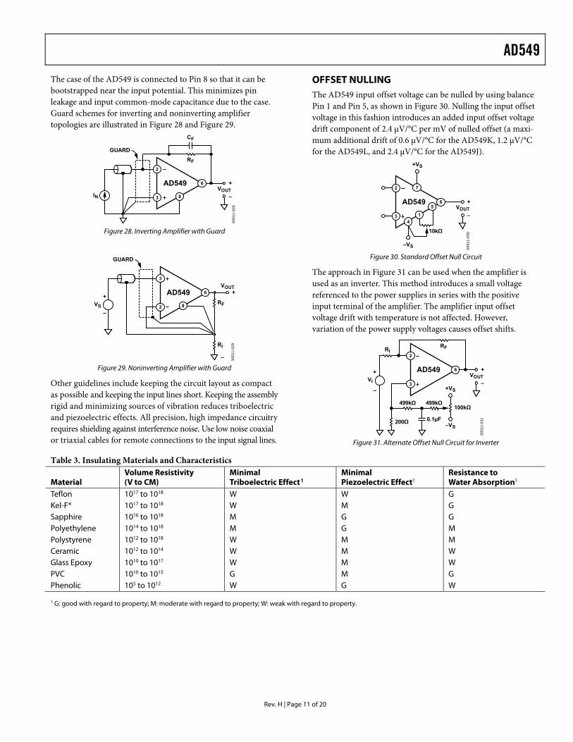
AD549
Rev. H | Page 11 of 20
The case of the AD549 is connected to Pin 8 so that it can be bootstrapped near the input potential. This minimizes pin leakage and input common-mode capacitance due to the case. Guard schemes for inverting and noninverting amplifier topologies are illustrated in Figure 28 and Figure 29.
0051
1-02
8
2
3
6
8
AD549 +VOUT
–IN
CF
RF
GUARD
Figure 28. Inverting Amplifier with Guard
0051
1-02
9
3
2
6
8
AD549 +VOUT
–
VS
+
–
GUARD
RF
RI
Figure 29. Noninverting Amplifier with Guard
Other guidelines include keeping the circuit layout as compact as possible and keeping the input lines short. Keeping the assembly rigid and minimizing sources of vibration reduces triboelectric and piezoelectric effects. All precision, high impedance circuitry requires shielding against interference noise. Use low noise coaxial or triaxial cables for remote connections to the input signal lines.
OFFSET NULLING The AD549 input offset voltage can be nulled by using balance Pin 1 and Pin 5, as shown in Figure 30. Nulling the input offset voltage in this fashion introduces an added input offset voltage drift component of 2.4 μV/°C per mV of nulled offset (a maxi-mum additional drift of 0.6 μV/°C for the AD549K, 1.2 μV/°C for the AD549L, and 2.4 μV/°C for the AD549J).
0051
1-03
0
2
3
65
1
7
4
AD549 +VOUT
–
–VS
+VS
10kΩ
Figure 30. Standard Offset Null Circuit
The approach in Figure 31 can be used when the amplifier is used as an inverter. This method introduces a small voltage referenced to the power supplies in series with the positive input terminal of the amplifier. The amplifier input offset voltage drift with temperature is not affected. However, variation of the power supply voltages causes offset shifts.
0051
1-03
1
2
3
6AD549 +VOUT
–VI
+
–
RFRI
200Ω
100kΩ499kΩ 499kΩ
0.1µF–VS
+VS
Figure 31. Alternate Offset Null Circuit for Inverter
Table 3. Insulating Materials and Characteristics
Material Volume Resistivity (V to CM)
Minimal Triboelectric Effect1
Minimal Piezoelectric Effect1
Resistance to Water Absorption1
Teflon 1017 to 1018 W W G Kel-F® 1017 to 1018 W M G Sapphire 1016 to 1018 M G G Polyethylene 1014 to 1018 M G M Polystyrene 1012 to 1018 W M M Ceramic 1012 to 1014 W M W Glass Epoxy 1010 to 1017 W M W PVC 1010 to 1015 G M G Phenolic 105 to 1012 W G W 1 G: good with regard to property; M: moderate with regard to property; W: weak with regard to property.
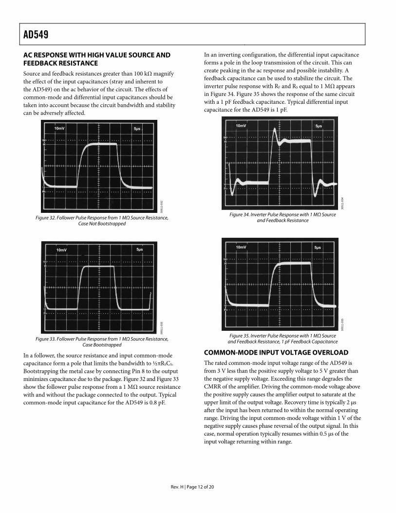
AD549
Rev. H | Page 12 of 20
AC RESPONSE WITH HIGH VALUE SOURCE AND FEEDBACK RESISTANCE Source and feedback resistances greater than 100 kΩ magnify the effect of the input capacitances (stray and inherent to the AD549) on the ac behavior of the circuit. The effects of common-mode and differential input capacitances should be taken into account because the circuit bandwidth and stability can be adversely affected.
0051
1-03
2
10mV 5µs
Figure 32. Follower Pulse Response from 1 MΩ Source Resistance,
Case Not Bootstrapped
0051
1-03
3
10mV 5µs
Figure 33. Follower Pulse Response from 1 MΩ Source Resistance,
Case Bootstrapped
In a follower, the source resistance and input common-mode capacitance form a pole that limits the bandwidth to ½πRSCS. Bootstrapping the metal case by connecting Pin 8 to the output minimizes capacitance due to the package. Figure 32 and Figure 33 show the follower pulse response from a 1 MΩ source resistance with and without the package connected to the output. Typical common-mode input capacitance for the AD549 is 0.8 pF.
In an inverting configuration, the differential input capacitance forms a pole in the loop transmission of the circuit. This can create peaking in the ac response and possible instability. A feedback capacitance can be used to stabilize the circuit. The inverter pulse response with RF and RS equal to 1 MΩ appears in Figure 34. Figure 35 shows the response of the same circuit with a 1 pF feedback capacitance. Typical differential input capacitance for the AD549 is 1 pF.
0051
1-03
4
10mV 5µs
Figure 34. Inverter Pulse Response with 1 MΩ Source
and Feedback Resistance
0051
1-03
5
10mV 5µs
Figure 35. Inverter Pulse Response with 1 MΩ Source
and Feedback Resistance, 1 pF Feedback Capacitance
COMMON-MODE INPUT VOLTAGE OVERLOAD The rated common-mode input voltage range of the AD549 is from 3 V less than the positive supply voltage to 5 V greater than the negative supply voltage. Exceeding this range degrades the CMRR of the amplifier. Driving the common-mode voltage above the positive supply causes the amplifier output to saturate at the upper limit of the output voltage. Recovery time is typically 2 μs after the input has been returned to within the normal operating range. Driving the input common-mode voltage within 1 V of the negative supply causes phase reversal of the output signal. In this case, normal operation typically resumes within 0.5 μs of the input voltage returning within range.
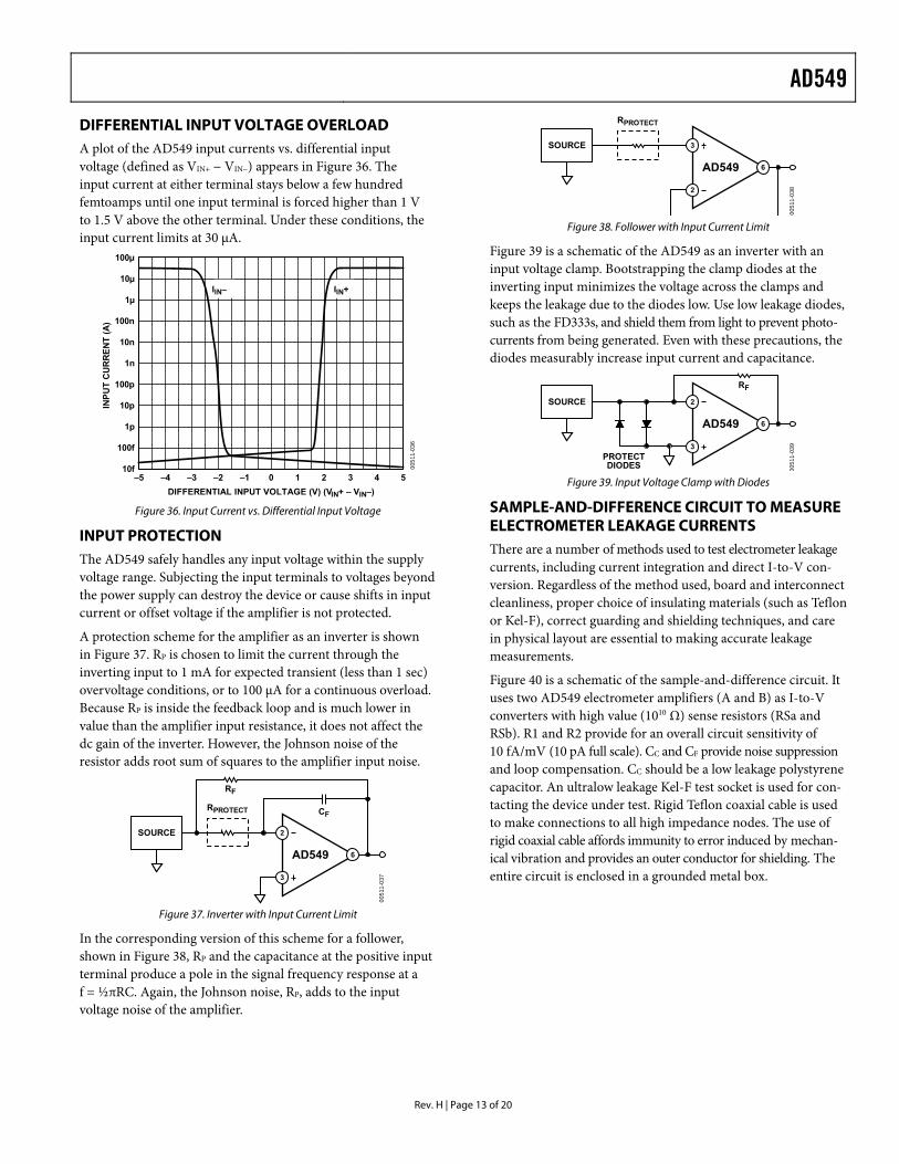
AD549
Rev. H | Page 13 of 20
0051
1-03
8
3
2
6AD549
SOURCE
RPROTECT
DIFFERENTIAL INPUT VOLTAGE OVERLOAD A plot of the AD549 input currents vs. differential input voltage (defined as VIN+ − VIN−) appears in Figure 36. The input current at either terminal stays below a few hundred femtoamps until one input terminal is forced higher than 1 V to 1.5 V above the other terminal. Under these conditions, the input current limits at 30 μA.
Figure 38. Follower with Input Current Limit
Figure 39 is a schematic of the AD549 as an inverter with an input voltage clamp. Bootstrapping the clamp diodes at the inverting input minimizes the voltage across the clamps and keeps the leakage due to the diodes low. Use low leakage diodes, such as the FD333s, and shield them from light to prevent photo-currents from being generated. Even with these precautions, the diodes measurably increase input current and capacitance.
100µ
10µ
1µ
100n
10n
1n
100p
10p
1p
100f
10f–5 –4 –3 –2 –1 0 1 2 3 4 5
0051
1-03
6
DIFFERENTIAL INPUT VOLTAGE (V) (VIN+ – VIN–)
INPU
T C
UR
REN
T (A
)
IIN– IIN+
0051
1-03
9
2
3
6AD549
SOURCE
RF
PROTECTDIODES
Figure 39. Input Voltage Clamp with Diodes
SAMPLE-AND-DIFFERENCE CIRCUIT TO MEASURE ELECTROMETER LEAKAGE CURRENTS
Figure 36. Input Current vs. Differential Input Voltage
INPUT PROTECTION There are a number of methods used to test electrometer leakage currents, including current integration and direct I-to-V con-version. Regardless of the method used, board and interconnect cleanliness, proper choice of insulating materials (such as Teflon or Kel-F), correct guarding and shielding techniques, and care in physical layout are essential to making accurate leakage measurements.
The AD549 safely handles any input voltage within the supply voltage range. Subjecting the input terminals to voltages beyond the power supply can destroy the device or cause shifts in input current or offset voltage if the amplifier is not protected.
A protection scheme for the amplifier as an inverter is shown in Figure 37. RP is chosen to limit the current through the inverting input to 1 mA for expected transient (less than 1 sec) overvoltage conditions, or to 100 μA for a continuous overload. Because RP is inside the feedback loop and is much lower in value than the amplifier input resistance, it does not affect the dc gain of the inverter. However, the Johnson noise of the resistor adds root sum of squares to the amplifier input noise.
Figure 40 is a schematic of the sample-and-difference circuit. It uses two AD549 electrometer amplifiers (A and B) as I-to-V converters with high value (1010 Ω) sense resistors (RSa and RSb). R1 and R2 provide for an overall circuit sensitivity of 10 fA/mV (10 pA full scale). CC and CF provide noise suppression and loop compensation. CC should be a low leakage polystyrene capacitor. An ultralow leakage Kel-F test socket is used for con-tacting the device under test. Rigid Teflon coaxial cable is used to make connections to all high impedance nodes. The use of rigid coaxial cable affords immunity to error induced by mechan-ical vibration and provides an outer conductor for shielding. The entire circuit is enclosed in a grounded metal box.
0051
1-03
7
2
3
6AD549
CF
SOURCE
RPROTECT
RF
Figure 37. Inverter with Input Current Limit
In the corresponding version of this scheme for a follower, shown in Figure 38, RP and the capacitance at the positive input terminal produce a pole in the signal frequency response at a f = ½πRC. Again, the Johnson noise, RP, adds to the input voltage noise of the amplifier.
AD549
Rev. H | Page 14 of 20
The test apparatus is calibrated without a device under test present. After power is turned on, a 5 minute stabilization period is required. First, VERR1 and VERR2 are measured. These voltages are the errors caused by the offset voltages and leakage currents of the I-to-V converters.
VERR1 = 10 (VOSA – IBA × RSa)
VERR2 = 10 (VOSB – IBB × RSb)
0051
1-04
0
VOS+
–
2
3
6
8
AAD549
R29.01kΩ
R11kΩ
RSa1010Ω
+VERR1/VA
VERR2/VB
VOUT
–
CAL/TEST
CC20pF
CF0.1µF
+
–
3
2
6
8
BAD549
R29.01kΩ
R11kΩ
RSb1010Ω
CC20pF
CF0.1µF
CF0.1µF
R11kΩ
R29.01kΩ
DEVICEUNDERTEST
I (+)
I (–)
GUARD
Figure 40. Sample and Difference Circuit for Measuring
Electrometer Leakage Currents
Once measured, these errors are subtracted from the readings taken with a device under test present. Amplifier B closes the feedback loop to the device under testing in addition to pro-viding the I-to-V conversion. The offset error of the device under testing appears as a common-mode signal and does not affect the test measurement. As a result, only the leakage current of the device under testing is measured.
VA – VERR1 = 10[RSa × IB(+)]
VX – VERR2 = 10[RSb × IB(–)]
Although a series of devices can be tested after only one calibra-tion measurement, calibration should be updated periodically to compensate for any thermal drift of the I-to-V converters or changes in the ambient environment. Laboratory results have shown that repeatable measurements within 10 fA can be realized when this apparatus is properly implemented. These results are achieved in part by the design of the circuit, which eliminates relays and other parasitic leakage paths in the high impedance signal lines, and in part by the inherent cancellation of errors through the calibration and measurement procedure.
PHOTODIODE INTERFACE The low input current and low input offset voltage of the AD549 make it an excellent choice for very sensitive photodiode preamps (see Figure 41). The photodiode develops a signal current, IS, equal to
IS = R × P
where P is light power incident on the diode surface, in watts, and R is the photodiode responsivity in amps/watt. RF converts the signal current to an output voltage
VOUT = RF × IS
0051
1-04
1
2
3
65
14
AD549
–VS
CF10pF
IS
RF109Ω
10kΩ
1µF VOUT
+
–
Figure 41. Photodiode Preamp
The dc error sources and an equivalent circuit for a small area (0.2 mm square) photodiode are indicated in Figure 42.
0051
1-04
2
A +VOUT
–VOS+–
IS–IS RS109Ω
CS20pF
RF109Ω
CF10pF
Figure 42. Photodiode Preamp DC Error Sources
AD549
Rev. H | Page 15 of 20
gain that multiplies the op amp input voltage noise contribu-tion. A single-pole filter at the output of the amplifier limits the op amp output voltage noise bandwidth to 26 Hz, comparable to the signal bandwidth. This greatly improves the signal-to-noise ratio of the preamplifier (in this case, by a factor of 3).
Input current, IB, contributes an output voltage error, VE1, proportional to the feedback resistance
VE1 = IB × RF
The input voltage offset of the op amp causes an error current through the photodiode shunt resistance, RS 10µ
1µ
100n
10n1 10 100 1k 10k 100k 1M
0051
1-04
4
FREQUENCY (Hz)
VOLT
AG
E N
OIS
E C
ON
TRIB
UTI
ON
SN
OIS
E SP
ECTR
AL
DEN
SITY
(nV/
Hz)
IF AND CS, NO FILTERS
IF AND CS, WITH FILTERS
ENCONTRIBUTION,WITH FILTER
EN CONTRIBUTION,NO FILTER
AD549OPEN-LOOP GAIN
I = VOS/RS
The error current results in an error voltage (VE2) at the amplifier output equal to
VE2 = (1 + RF/RS)VOS
Given typical values of photodiode shunt resistance (on the order of 109 Ω), RF/RS can easily be greater than 1, especially if a large feedback resistance is used. Also, RF/RS increases with tempera-ture because photodiode shunt resistance typically drops by a factor of 2 for every 10°C rise in temperature. An op amp with low offset voltage and low drift must be used to maintain accuracy. The AD549K offers a guaranteed maximum 0.25 mV offset voltage and 5 mV/°C drift for very sensitive applications.
Figure 44. Spectral Density of the Photodiode Preamp Noise Sources vs. Frequency
Photodiode Preamp Noise
Noise limits the signal resolution obtainable with the preamp. The output voltage noise divided by the feedback resistance is the minimum current signal that can be detected. This mini-mum detectable current divided by the responsivity of the photodiode represents the lowest light power that is detectable by the preamp.
LOG RATIO AMPLIFIER Logarithmic ratio circuits are useful for processing signals with wide dynamic range. The 60 fA maximum input current of the AD549L makes it possible to build a log ratio amplifier with 1% log conformance for input currents ranging from 10 pA to 1 mA, a dynamic range of 160 dB. Noise sources associated with the photodiode, amplifier, and
feedback resistance are shown in Figure 43; Figure 44 is the spectral density vs. frequency plot of the contribution of each of the noise sources to the output voltage noise (circuit parameters in Figure 42 are assumed). The rms contribution of each noise source to the total output voltage noise is obtained by integrating the square of its spectral density function over frequency. The rms value of the output voltage noise is the square root of the sum of all contributions. Minimizing the total area under these curves optimizes the resolution of the preamplifier for a given bandwidth.
The log ratio amplifier in Figure 45 provides an output voltage proportional to the log base 10 of the ratio of Input Current I1 and Input Current I2. Resistor R1 and Resistor R2 are provided for voltage inputs. Because NPN devices are used in the feedback loop of the front-end amplifiers that provide the log transfer function, the output is valid only for positive input voltages and input currents. The input currents set the Collector Current IC1 and Collector Current IC2 of a matched pair of log transistors, Q1 and Q2, to develop Voltage VA and Voltage VB
VA, VB = –(kT/q)ln IC/IES
0051
1-04
3
AIS RS CS
CF
RF
IF
EN
IN
where IES is the saturation current of the transistor.
The difference of VA and VB is taken by the subtractor section to obtain
VC = (kT/q)ln(IC2/IC1)
VC is scaled up by the ratio of (R9 + R10)/R8, which is equal to approximately 16 at room temperature, resulting in the output voltage
Figure 43. Photodiode Preamp Noise Sources VOUT = 1 V × log(IC2/IC1)
The photodiode preamp in Figure 41 can detect a signal current of 26 fA rms at a bandwidth of 16 Hz, which, assuming a photodiode responsivity of 0.5 A/W, translates to a 52 fW rms minimum detectable power. The photodiode used has a high source resistance and low junction capacitance. CF sets the signal bandwidth with RF and also limits the peak in the noise
R8 is a resistor with a positive 3500 ppm/°C temperature coeffi-cient to provide the necessary temperature compensation. The parallel combination of R15 and R7 is provided to keep the gain of the subtractor section for positive and negative inputs matched over temperature.
AD549
Rev. H | Page 16 of 20
Frequency compensation is provided by R11, R12, C1, and C2. The bandwidth of the circuit is 300 kHz at input signals greater than 50 μA; bandwidth decreases smoothly with decreasing signal levels.
To trim the circuit, set the input currents to 10 μA and trim the A3 offset using the trim potentiometer of the amplifier for the output to equal 0. Next, set I1 to 1 μA and adjust the output to equal 1 V by trimming R10. Additional offset trims on Ampli-fier A1 and Amplifier A2 can be used to increase the voltage input accuracy and dynamic range.
The very low input current of the AD549 makes this circuit useful over a very wide range of signal currents. The total input current (which determines the low level accuracy of the circuit) is the sum of the amplifier input current, the leakage across the compensating capacitor (negligible if a polystyrene or Teflon capacitor is used), and the collector-to-collector and collector-to-base leakages of one side of the dual log transistors. The magnitudes of these last two leakages depend on the amplifier input offset voltage and are typically less than 10 fA with 1 mV offsets. The low level accuracy is limited primarily by the amplifier input current, only 60 fA maximum when the AD549L is used.
The effects of the emitter resistance of Q1 and Q2 can degrade circuit accuracy at input currents above 100 μA. The networks
composed of R13, D1, R16, R14, D2, and R17 compensate for these errors, so that this circuit has less than a 1% log confor-mance error at 1 mA input currents. The correct value for R13 and R14 depends on the type of log transistors used. The 49.9 kΩ resistors were chosen for use with LM394 transistors. Smaller resistance values are needed for smaller log transistors.
TEMPERATURE COMPENSATED pH PROBE AMPLIFIER A pH probe can be modeled as an mV-level voltage source with a series source resistance dependent on the electrode composition and configuration. The glass bulb resistance of a typical pH electrode pair falls between 106 Ω and 109 Ω. It is therefore important to select an amplifier with low enough input currents such that the voltage drop produced by the amplifier input bias current and the electrode resistance does not become an appreciable percentage of a pH unit.
The circuit in Figure 46 illustrates the use of the AD549 as a pH probe amplifier. As with other electrometer applications, the use of guarding, shielding, and Teflon standoffs is necessary to capitalize on the AD549 low input current. If an AD549L (60 fA maximum input current) is used, the error contributed by the input current is held below 60 μV for pH electrode source impedances up to 109 Ω. Input offset voltages (which can be trimmed) are below 0.5 mV.
0051
1-04
5
3
2
65
14
A3AD549
R102kΩ10kΩ
OUTPUTOFFSET
SCALEFACTORADJ
VOUT
R914.3kΩR8
1kΩ*
*
R420kΩ
4.99kΩ
R620kΩ
R715kΩ
R151kΩ
R520kΩ
R320kΩ
0.1µF
0.1µF
+VS
FOR EACH AMPLIFIERPIN 7
PIN 4 –VS
2
3
65
14
A2AD549
V2OFFSET
10kΩ
D4I2 IN
V2 INC2
100pF
R210kΩ
Q2B
D2
D1
I1 IN 2
65
14
A1AD549
V1OFFSET
10kΩ
D33
V1 IN
R110kΩ
Q1A
C1100pF
R114.99kΩ
R1449.9kΩ
R1610Ω
R1710Ω
R1349.9kΩ
Q1, Q2 = LM394DUAL LOG TRANSISTORS
D1, D4 1N4148 DIODESR8, R15 1kΩ + 350 ppm/°C TC RESISTOR*TELLAB QB1 OR PRECISION RESISTOR PT146ALL OTHER RESISTORS ARE 1% METAL FILM
VOUT = 1V × LOG10V2V1
VOUT = 1V × LOG10I2I1
Figure 45. Log Ratio Amplifier
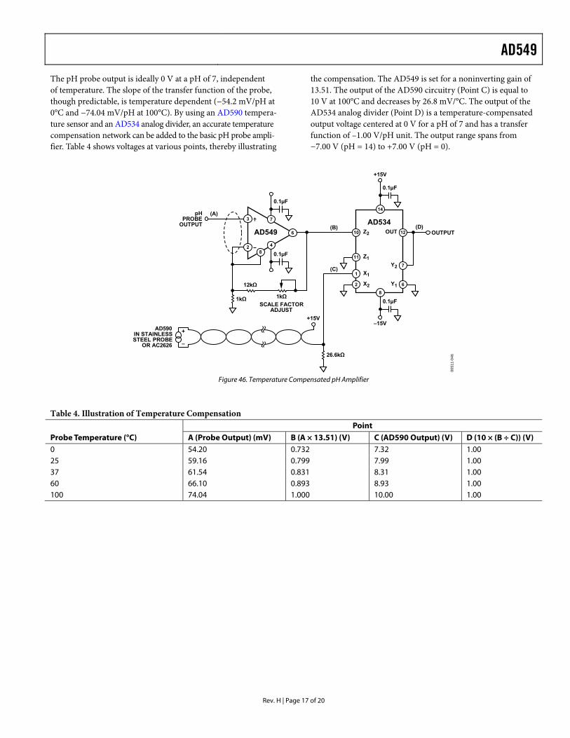
AD549
Rev. H | Page 17 of 20
The pH probe output is ideally 0 V at a pH of 7, independent of temperature. The slope of the transfer function of the probe, though predictable, is temperature dependent (−54.2 mV/pH at 0°C and −74.04 mV/pH at 100°C). By using an AD590 tempera-ture sensor and an AD534 analog divider, an accurate temperature compensation network can be added to the basic pH probe ampli-fier. Table 4 shows voltages at various points, thereby illustrating
the compensation. The AD549 is set for a noninverting gain of 13.51. The output of the AD590 circuitry (Point C) is equal to 10 V at 100°C and decreases by 26.8 mV/°C. The output of the AD534 analog divider (Point D) is a temperature-compensated output voltage centered at 0 V for a pH of 7 and has a transfer function of –1.00 V/pH unit. The output range spans from −7.00 V (pH = 14) to +7.00 V (pH = 0).
0051
1-04
6
8
14
10 Z2 12OUT
7Y2
6Y1
11 Z1
1 X1
2 X2
AD534
0.1µF
+15V
0.1µF
–15V
OUTPUT(D)(B)
(C)
26.6kΩ
+
–
AD590IN STAINLESSSTEEL PROBE
OR AC2626
+15V
3
2
6
48
7
AD549
0.1µF
0.1µF
pHPROBE
OUTPUT
(A)
1kΩ
12kΩ
1kΩSCALE FACTOR
ADJUST
Figure 46. Temperature Compensated pH Amplifier
Table 4. Illustration of Temperature Compensation Point Probe Temperature (°C) A (Probe Output) (mV) B (A × 13.51) (V) C (AD590 Output) (V) D (10 × (B ÷ C)) (V) 0 54.20 0.732 7.32 1.00 25 59.16 0.799 7.99 1.00 37 61.54 0.831 8.31 1.00 60 66.10 0.893 8.93 1.00 100 74.04 1.000 10.00 1.00
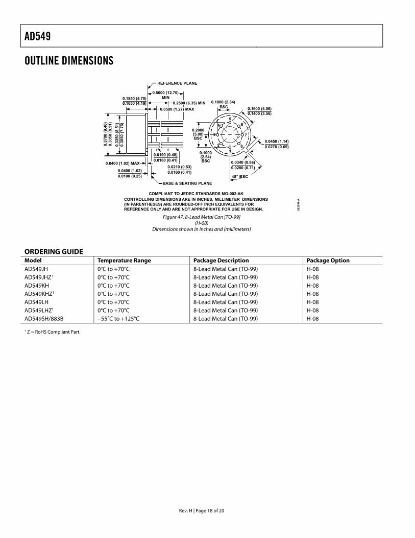
AD549
Rev. H | Page 18 of 20
OUTLINE DIMENSIONS
CONTROLLING DIMENSIONS ARE IN INCHES; MILLIMETER DIMENSIONS(IN PARENTHESES) ARE ROUNDED-OFF INCH EQUIVALENTS FORREFERENCE ONLY AND ARE NOT APPROPRIATE FOR USE IN DESIGN.
COMPLIANT TO JEDEC STANDARDS MO-002-AK
0.2500 (6.35) MIN
0.5000 (12.70)MIN0.1850 (4.70)
0.1650 (4.19)
REFERENCE PLANE
0.0500 (1.27) MAX
0.0190 (0.48)0.0160 (0.41)
0.0210 (0.53)0.0160 (0.41)0.0400 (1.02)
0.0100 (0.25)
0.0400 (1.02) MAX 0.0340 (0.86)0.0280 (0.71)
0.0450 (1.14)0.0270 (0.69)
0.1600 (4.06)0.1400 (3.56)
0.1000 (2.54)BSC
6
2 8
7
54
3
1
0.2000(5.08)BSC
0.1000(2.54)BSC
0.37
00 (9
.40)
0.33
50 (8
.51)
0.33
50 (8
.51)
0.30
50 (7
.75)
45° BSCBASE & SEATING PLANE
0223
06-A
Figure 47. 8-Lead Metal Can [TO-99]
(H-08) Dimensions shown in inches and (millimeters)
ORDERING GUIDE Model Temperature Range Package Description Package Option AD549JH 0°C to +70°C 8-Lead Metal Can (TO-99) H-08 AD549JHZ1
0°C to +70°C 8-Lead Metal Can (TO-99) H-08 AD549KH 0°C to +70°C 8-Lead Metal Can (TO-99) H-08 AD549KHZ1
0°C to +70°C 8-Lead Metal Can (TO-99) H-08 AD549LH 0°C to +70°C 8-Lead Metal Can (TO-99) H-08 AD549LHZ1
0°C to +70°C 8-Lead Metal Can (TO-99) H-08 AD549SH/883B −55°C to +125°C 8-Lead Metal Can (TO-99) H-08 1 Z = RoHS Compliant Part.

AD549
Rev. H | Page 19 of 20
NOTES

AD549
Rev. H | Page 20 of 20
NOTES
©2002–2008 Analog Devices, Inc. All rights reserved. Trademarks and registered trademarks are the property of their respective owners. D00511-0-3/08(H)
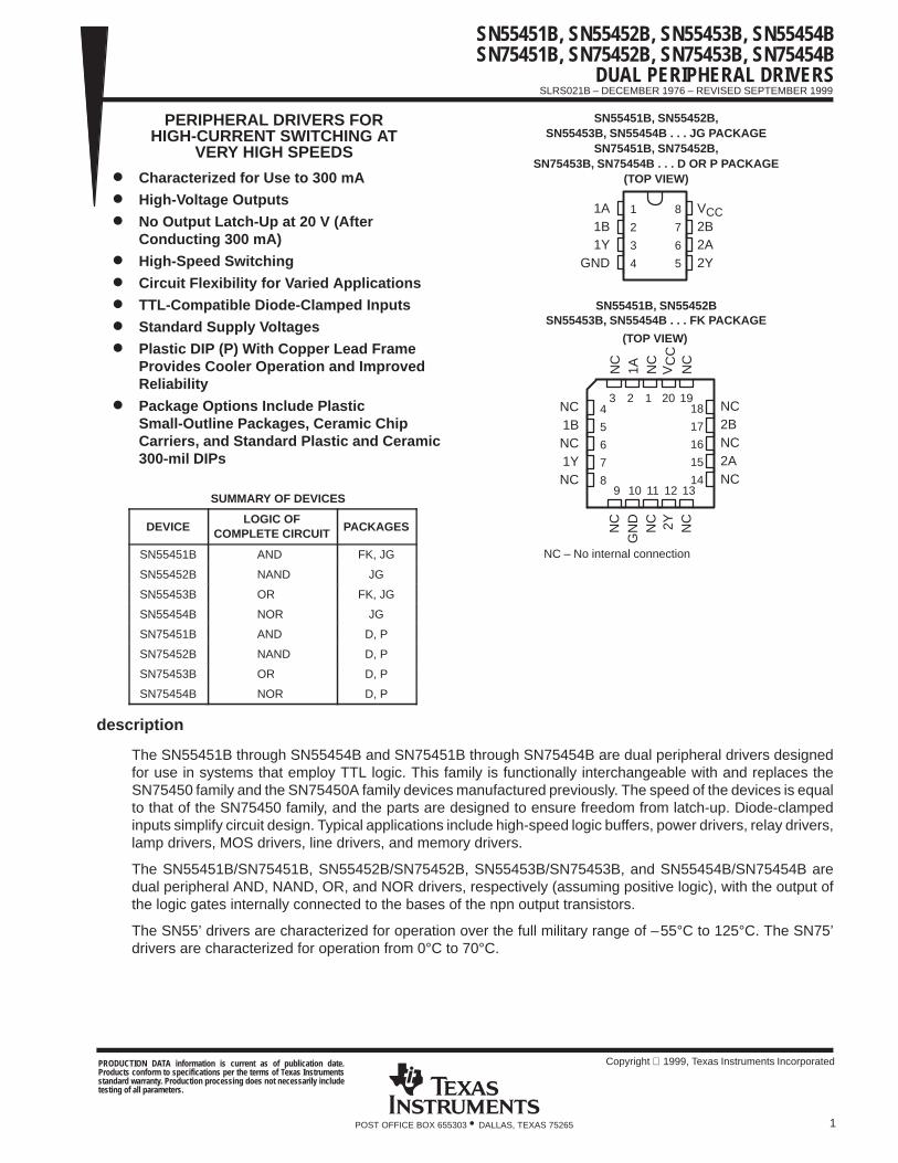
SN55451B, SN55452B, SN55453B, SN55454BSN75451B, SN75452B, SN75453B, SN75454B
DUAL PERIPHERAL DRIVERS
SLRS021B – DECEMBER 1976 – REVISED SEPTEMBER 1999
1POST OFFICE BOX 655303 • DALLAS, TEXAS 75265
PERIPHERAL DRIVERS FORHIGH-CURRENT SWITCHING AT
VERY HIGH SPEEDS
Characterized for Use to 300 mA
High-Voltage Outputs
No Output Latch-Up at 20 V (AfterConducting 300 mA)
High-Speed Switching
Circuit Flexibility for Varied Applications
TTL-Compatible Diode-Clamped Inputs
Standard Supply Voltages
Plastic DIP (P) With Copper Lead FrameProvides Cooler Operation and ImprovedReliability
Package Options Include PlasticSmall-Outline Packages, Ceramic ChipCarriers, and Standard Plastic and Ceramic300-mil DIPs
SUMMARY OF DEVICES
DEVICELOGIC OF
COMPLETE CIRCUIT PACKAGES
SN55451B AND FK, JG
SN55452B NAND JG
SN55453B OR FK, JG
SN55454B NOR JG
SN75451B AND D, P
SN75452B NAND D, P
SN75453B OR D, P
SN75454B NOR D, P
description
The SN55451B through SN55454B and SN75451B through SN75454B are dual peripheral drivers designedfor use in systems that employ TTL logic. This family is functionally interchangeable with and replaces theSN75450 family and the SN75450A family devices manufactured previously. The speed of the devices is equalto that of the SN75450 family, and the parts are designed to ensure freedom from latch-up. Diode-clampedinputs simplify circuit design. Typical applications include high-speed logic buffers, power drivers, relay drivers,lamp drivers, MOS drivers, line drivers, and memory drivers.
The SN55451B/SN75451B, SN55452B/SN75452B, SN55453B/SN75453B, and SN55454B/SN75454B aredual peripheral AND, NAND, OR, and NOR drivers, respectively (assuming positive logic), with the output ofthe logic gates internally connected to the bases of the npn output transistors.
The SN55’ drivers are characterized for operation over the full military range of –55°C to 125°C. The SN75’drivers are characterized for operation from 0°C to 70°C.
Copyright 1999, Texas Instruments IncorporatedPRODUCTION DATA information is current as of publication date.Products conform to specifications per the terms of Texas Instrumentsstandard warranty. Production processing does not necessarily includetesting of all parameters.
1
2
3
4
8
7
6
5
1A1B1Y
GND
VCC2B2A2Y
SN55451B, SN55452B,SN55453B, SN55454B . . . JG PACKAGE
SN75451B, SN75452B,SN75453B, SN75454B . . . D OR P PACKAGE
(TOP VIEW)
3 2 1 20 19
9 10 11 12 13
4
5
6
7
8
18
17
16
15
14
NC2BNC2ANC
NC1BNC1YNC
SN55451B, SN55452BSN55453B, SN55454B . . . FK PACKAGE
(TOP VIEW)
NC
1A NC
NC
NC
NC
GN
DN
C
NC – No internal connection
CC
V2Y
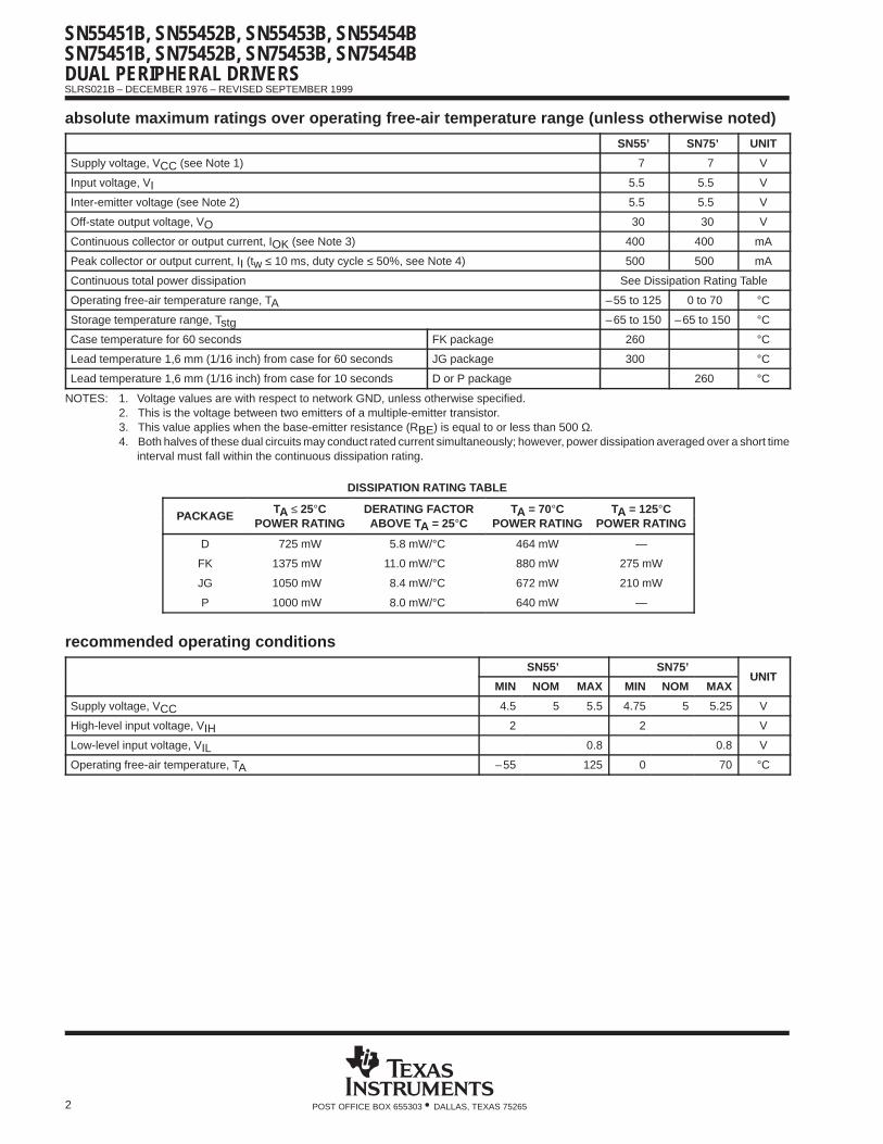
SN55451B, SN55452B, SN55453B, SN55454BSN75451B, SN75452B, SN75453B, SN75454BDUAL PERIPHERAL DRIVERS
SLRS021B – DECEMBER 1976 – REVISED SEPTEMBER 1999
2 POST OFFICE BOX 655303 • DALLAS, TEXAS 75265
absolute maximum ratings over operating free-air temperature range (unless otherwise noted)
SN55’ SN75’ UNIT
Supply voltage, VCC (see Note 1) 7 7 V
Input voltage, VI 5.5 5.5 V
Inter-emitter voltage (see Note 2) 5.5 5.5 V
Off-state output voltage, VO 30 30 V
Continuous collector or output current, IOK (see Note 3) 400 400 mA
Peak collector or output current, II (tw ≤ 10 ms, duty cycle ≤ 50%, see Note 4) 500 500 mA
Continuous total power dissipation See Dissipation Rating Table
Operating free-air temperature range, TA –55 to 125 0 to 70 °C
Storage temperature range, Tstg –65 to 150 –65 to 150 °C
Case temperature for 60 seconds FK package 260 °C
Lead temperature 1,6 mm (1/16 inch) from case for 60 seconds JG package 300 °C
Lead temperature 1,6 mm (1/16 inch) from case for 10 seconds D or P package 260 °C
NOTES: 1. Voltage values are with respect to network GND, unless otherwise specified.2. This is the voltage between two emitters of a multiple-emitter transistor.3. This value applies when the base-emitter resistance (RBE) is equal to or less than 500 Ω.4. Both halves of these dual circuits may conduct rated current simultaneously; however, power dissipation averaged over a short time
interval must fall within the continuous dissipation rating.
DISSIPATION RATING TABLE
PACKAGETA ≤ 25°C DERATING FACTOR TA = 70°C TA = 125°C
PACKAGE APOWER RATING ABOVE TA = 25°C
APOWER RATING
APOWER RATING
D 725 mW 5.8 mW/°C 464 mW —
FK 1375 mW 11.0 mW/°C 880 mW 275 mW
JG 1050 mW 8.4 mW/°C 672 mW 210 mW
P 1000 mW 8.0 mW/°C 640 mW —
recommended operating conditions
SN55’ SN75’UNIT
MIN NOM MAX MIN NOM MAXUNIT
Supply voltage, VCC 4.5 5 5.5 4.75 5 5.25 V
High-level input voltage, VIH 2 2 V
Low-level input voltage, VIL 0.8 0.8 V
Operating free-air temperature, TA –55 125 0 70 °C
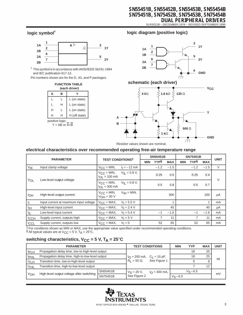
SN55451B, SN55452B, SN55453B, SN55454BSN75451B, SN75452B, SN75453B, SN75454B
DUAL PERIPHERAL DRIVERS
SLRS021B – DECEMBER 1976 – REVISED SEPTEMBER 1999
3POST OFFICE BOX 655303 • DALLAS, TEXAS 75265
logic symbol †
&
5
3
2B
2A
1B
1A
2Y
1Y
7
6
2
1
† This symbol is in accordance with ANSI/IEEE Std 91-1984and IEC publication 617-12.
Pin numbers shown are for the D, JG, and P packages.
logic diagram (positive logic)
2B
2A
1B
1A
4
5
3
GND
2Y
1Y
7
6
2
1
FUNCTION TABLE (each driver)
A B Y
L L L (on state)
L H L (on state)
H L L (on state)
H H H (off state)
positive logic:Y = AB or A+B
electrical characteristics over recommended operating free-air temperature range
PARAMETER TEST CONDITIONS‡SN55451B SN75451B
UNITPARAMETER TEST CONDITIONS‡MIN TYP§ MAX MIN TYP§ MAX
UNIT
VIK Input clamp voltage VCC = MIN, II = –12 mA –1.2 –1.5 –1.2 –1.5 V
VCC = MIN, VIL = 0.8 V,0 25 0 5 0 25 0 4
VOL Low level output voltage
CCIOL = 100 mA
IL 0.25 0.5 0.25 0.4
VVOL Low-level output voltageVCC = MIN, VIL = 0.8 V,
0 5 0 8 0 5 0 7
VCC
IOL = 300 mAIL 0.5 0.8 0.5 0.7
IOH High level output currentVCC = MIN, VIH = MIN,
300 100 µAIOH High-level output current CCVOH = 30 V
IH 300 100 µA
II Input current at maximum input voltage VCC = MAX, VI = 5.5 V 1 1 mA
IIH High-level input current VCC = MAX, VI = 2.4 V 40 40 µA
IIL Low-level input current VCC = MAX, VI = 0.4 V –1 –1.6 –1 –1.6 mA
ICCH Supply current, outputs high VCC = MAX, VI = 5 V 7 11 7 11 mA
ICCL Supply current, outputs low VCC = MAX, VI = 0 52 65 52 65 mA
‡ For conditions shown as MIN or MAX, use the appropriate value specified under recommended operating conditions.§ All typical values are at VCC = 5 V, TA = 25°C.
switching characteristics, V CC = 5 V, TA = 25°CPARAMETER TEST CONDITIONS MIN TYP MAX UNIT
tPLH Propagation delay time, low-to-high-level output 18 25
tPHL Propagation delay time, high-to-low-level output IO ≈ 200 mA, CL = 15 pF, 18 25ns
tTLH Transition time, low-to-high-level outputORL = 50 Ω,
LSee Figure 1 5 8
ns
tTHL Transition time, high-to-low-level output 7 12
VOH High level output voltage after switchingSN55451B VS = 20 V, IO ≈ 300 mA, VS–6.5
mVVOH High-level output voltage after switchingSN75451B
S ,See Figure 2
O ,VS–6.5
mV
VCC
A
GND
Y
500 Ω1 kΩ
B
4 kΩ 1.6 kΩ 130 Ω
Resistor values shown are nominal.
schematic (each driver)
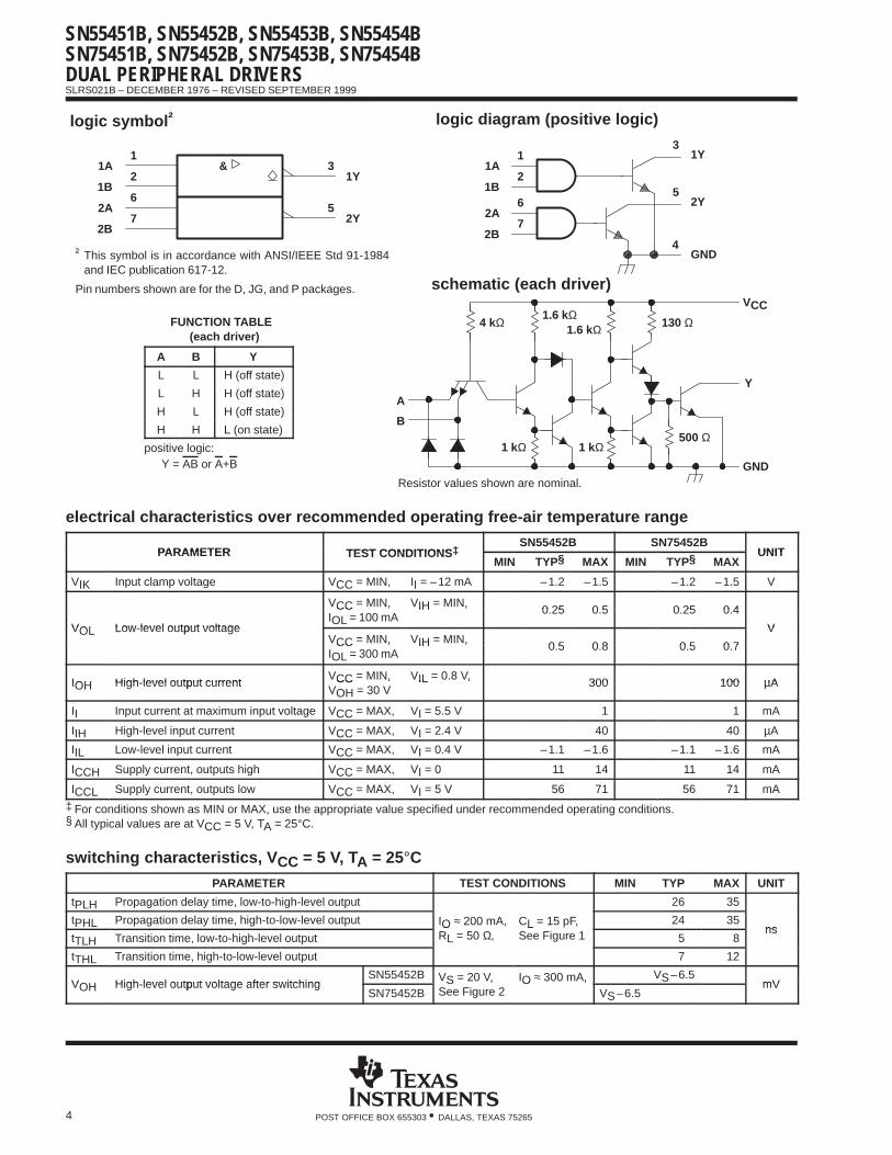
SN55451B, SN55452B, SN55453B, SN55454BSN75451B, SN75452B, SN75453B, SN75454BDUAL PERIPHERAL DRIVERS
SLRS021B – DECEMBER 1976 – REVISED SEPTEMBER 1999
4 POST OFFICE BOX 655303 • DALLAS, TEXAS 75265
logic symbol †
&
5
3
2B
2A
1B
1A
2Y
1Y
7
6
2
1
† This symbol is in accordance with ANSI/IEEE Std 91-1984and IEC publication 617-12.
Pin numbers shown are for the D, JG, and P packages.
logic diagram (positive logic)
2B
2A
1B
1A
4
5
3
GND
2Y
1Y
7
6
2
1
FUNCTION TABLE (each driver)
A B Y
L L H (off state)
L H H (off state)
H L H (off state)
H H L (on state)
positive logic:Y = AB or A+B
electrical characteristics over recommended operating free-air temperature range
PARAMETER TEST CONDITIONS‡SN55452B SN75452B
UNITPARAMETER TEST CONDITIONS‡MIN TYP§ MAX MIN TYP§ MAX
UNIT
VIK Input clamp voltage VCC = MIN, II = –12 mA –1.2 –1.5 –1.2 –1.5 V
VCC = MIN, VIH = MIN,0 25 0 5 0 25 0 4
VOL Low level output voltage
CC ,IOL = 100 mA
IH ,0.25 0.5 0.25 0.4
VVOL Low-level output voltageVCC = MIN, VIH = MIN,
0 5 0 8 0 5 0 7
VCC ,
IOL = 300 mAIH ,
0.5 0.8 0.5 0.7
IOH High level output currentVCC = MIN, VIL = 0.8 V,
300 100 µAIOH High-level output current CC ,VOH = 30 V
IL ,300 100 µA
II Input current at maximum input voltage VCC = MAX, VI = 5.5 V 1 1 mA
IIH High-level input current VCC = MAX, VI = 2.4 V 40 40 µA
IIL Low-level input current VCC = MAX, VI = 0.4 V –1.1 –1.6 –1.1 –1.6 mA
ICCH Supply current, outputs high VCC = MAX, VI = 0 11 14 11 14 mA
ICCL Supply current, outputs low VCC = MAX, VI = 5 V 56 71 56 71 mA
‡ For conditions shown as MIN or MAX, use the appropriate value specified under recommended operating conditions.§ All typical values are at VCC = 5 V, TA = 25°C.
switching characteristics, V CC = 5 V, TA = 25°CPARAMETER TEST CONDITIONS MIN TYP MAX UNIT
tPLH Propagation delay time, low-to-high-level output 26 35
tPHL Propagation delay time, high-to-low-level output IO ≈ 200 mA, CL = 15 pF, 24 35ns
tTLH Transition time, low-to-high-level outputORL = 50 Ω,
LSee Figure 1 5 8
ns
tTHL Transition time, high-to-low-level output 7 12
VOH High level output voltage after switchingSN55452B VS = 20 V, IO ≈ 300 mA, VS–6.5
mVVOH High-level output voltage after switchingSN75452B
S ,See Figure 2
O ,VS–6.5
mV
VCC
A
GND
Y
500 Ω1 kΩ
B
4 kΩ1.6 kΩ
130 Ω
schematic (each driver)
Resistor values shown are nominal.
1 kΩ
1.6 kΩ
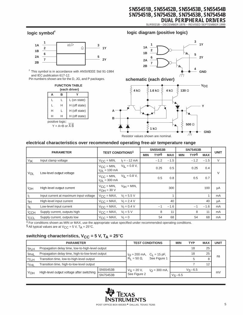
SN55451B, SN55452B, SN55453B, SN55454BSN75451B, SN75452B, SN75453B, SN75454B
DUAL PERIPHERAL DRIVERS
SLRS021B – DECEMBER 1976 – REVISED SEPTEMBER 1999
5POST OFFICE BOX 655303 • DALLAS, TEXAS 75265
logic symbol †
≥1
5
3
2B
2A
1B
1A
2Y
1Y
7
6
2
1
† This symbol is in accordance with ANSI/IEEE Std 91-1984and IEC publication 617-12.
Pin numbers shown are for the D, JG, and P packages.
logic diagram (positive logic)
2B
2A
1B
1A
4
5
3
GND
2Y
1Y
7
6
2
1
FUNCTION TABLE (each driver)
A B Y
L L L (on state)
L H H (off state)
H L H (off state)
H H H (off state)
positive logic:Y = A+B or A B
electrical characteristics over recommended operating free-air temperature range
PARAMETER TEST CONDITIONS‡SN55453B SN75453B
UNITPARAMETER TEST CONDITIONS‡MIN TYP§ MAX MIN TYP§ MAX
UNIT
VIK Input clamp voltage VCC = MIN, II = –12 mA –1.2 –1.5 –1.2 –1.5 V
VCC = MIN, VIL = 0.8 V,0 25 0 5 0 25 0 4
VOL Low level output voltage
CC ,IOL = 100 mA
IL 0.25 0.5 0.25 0.4
VVOL Low-level output voltageVCC = MIN, VIL = 0.8 V,
0 5 0 8 0 5 0 7
VCC ,
IOL = 300 mAIL 0.5 0.8 0.5 0.7
IOH High level output currentVCC = MIN, VIH = MIN,
300 100 µAIOH High-level output current CC ,VOH = 30 V
IH ,300 100 µA
II Input current at maximum input voltage VCC = MAX, VI = 5.5 V 1 1 mA
IIH High-level input current VCC = MAX, VI = 2.4 V 40 40 µA
IIL Low-level input current VCC = MAX, VI = 0.4 V –1 –1.6 –1 –1.6 mA
ICCH Supply current, outputs high VCC = MAX, VI = 5 V 8 11 8 11 mA
ICCL Supply current, outputs low VCC = MAX, VI = 0 54 68 54 68 mA
‡ For conditions shown as MIN or MAX, use the appropriate value specified under recommended operating conditions.§ All typical values are at VCC = 5 V, TA = 25°C.
switching characteristics, V CC = 5 V, TA = 25°CPARAMETER TEST CONDITIONS MIN TYP MAX UNIT
tPLH Propagation delay time, low-to-high-level output 18 25
tPHL Propagation delay time, high-to-low-level output IO ≈ 200 mA, CL = 15 pF, 18 25ns
tTLH Transition time, low-to-high-level outputO ,RL = 50 Ω,
L ,See Figure 1 5 8
ns
tTHL Transition time, high-to-low-level output 7 12
VOH High level output voltage after switchingSN55453B VS = 20 V, IO ≈ 300 mA, VS–6.5
mVVOH High-level output voltage after switchingSN75453B
SSee Figure 2
OVS–6.5
mV
schematic (each driver)
Resistor values shown are nominal.
VCC
A
GND
Y
500 Ω1 kΩ
B
4 kΩ 1.6 kΩ 130 Ω4 kΩ
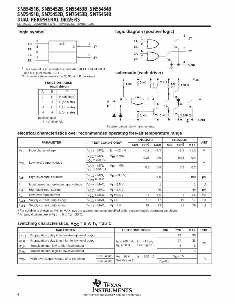
SN55451B, SN55452B, SN55453B, SN55454BSN75451B, SN75452B, SN75453B, SN75454BDUAL PERIPHERAL DRIVERS
SLRS021B – DECEMBER 1976 – REVISED SEPTEMBER 1999
6 POST OFFICE BOX 655303 • DALLAS, TEXAS 75265
logic symbol †
5
3
2B
2A
1B
1A
2Y
1Y
7
6
2
1
† This symbol is in accordance with ANSI/IEEE Std 91-1984and IEC publication 617-12.
Pin numbers shown are for the D, JG, and P packages.
≥1
logic diagram (positive logic)
2B
2A
1B
1A
4
5
3
GND
2Y
1Y
7
6
2
1
FUNCTION TABLE (each driver)
A B Y
L L H (off state)
L H L (on state)
H L L (on state)
H H L (on state)
positive logic:Y = A+B or AB
electrical characteristics over recommended operating free-air temperature range
PARAMETER TEST CONDITIONS‡SN55454B SN75454B
UNITPARAMETER TEST CONDITIONS‡MIN TYP§ MAX MIN TYP§ MAX
UNIT
VIK Input clamp voltage VCC = MIN, II = –12 mA –1.2 –1.5 –1.2 –1.5 V
VCC = MIN, VIH = MIN,0 25 0 5 0 25 0 4
VOL Low level output voltage
CC ,IOL = 100 mA
IH ,0.25 0.5 0.25 0.4
VVOL Low-level output voltageVCC = MIN, VIH = MIN,
0 5 0 8 0 5 0 7
VCC ,
IOL = 300 mAIH ,
0.5 0.8 0.5 0.7
IOH High level output currentVCC = MIN, VIL = 0.8 V,
300 100 µAIOH High-level output current CC ,VOH = 30 V
IL ,300 100 µA
II Input current at maximum input voltage VCC = MAX, VI = 5.5 V 1 1 mA
IIH High-level input current VCC = MAX, VI = 2.4 V 40 40 µA
IIL Low-level input current VCC = MAX, VI = 0.4 V –1 –1.6 –1 –1.6 mA
ICCH Supply current, outputs high VCC = MAX, VI = 0 13 17 13 17 mA
ICCL Supply current, outputs low VCC = MAX, VI = 5 V 61 79 61 79 mA
‡ For conditions shown as MIN or MAX, use the appropriate value specified under recommended operating conditions.§ All typical values are at VCC = 5 V, TA = 25°C.
switching characteristics, V CC = 5 V, TA = 25°CPARAMETER TEST CONDITIONS MIN TYP MAX UNIT
tPLH Propagation delay time, low-to-high-level output 27 35
tPHL Propagation delay time, high-to-low-level output IO ≈ 200 mA, CL = 15 pF, 24 35ns
tTLH Transition time, low-to-high-level outputO ,RL = 50 Ω,
L ,See Figure 1 5 8
ns
tTHL Transition time, high-to-low-level output 7 12
VOH High level output voltage after switchingSN55454B VS = 20 V, IO ≈ 300 mA, VS–6.5
mVVOH High-level output voltage after switchingSN75454B
SSee Figure 2
OVS–6.5
mV
4kΩ
1.6kΩ
2 kΩ
schematic (each driver)
Resistor values shown are nominal.
VCC
A
GND
Y
500 Ω1 kΩ
B
4 kΩ 2 kΩ130 Ω
1 kΩ
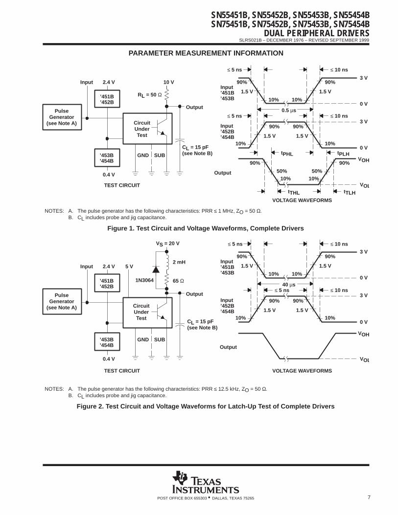
SN55451B, SN55452B, SN55453B, SN55454BSN75451B, SN75452B, SN75453B, SN75454B
DUAL PERIPHERAL DRIVERS
SLRS021B – DECEMBER 1976 – REVISED SEPTEMBER 1999
7POST OFFICE BOX 655303 • DALLAS, TEXAS 75265
PARAMETER MEASUREMENT INFORMATION
GND
PulseGenerator
(see Note A)
2.4 VInput
SUB
CircuitUnderTest
10% 10%
90%90%
1.5 V1.5 V
≤ 5 ns
90% 90%
10%10%
1.5 V1.5 V
0.5 µs
10% 10%
90%90%
50% 50%
tPHL tPLH
tTHL
3 V
0 V
3 V
0 V
VOH
VOL
Output
Input
TEST CIRCUIT
VOLTAGE WAVEFORMS
’451B’452B
’453B’454B
0.4 V
CL = 15 pF(see Note B)
Output
10 V
RL = 50 Ω
≤ 10 ns
≤ 5 ns ≤ 10 ns
tTLH
’451B’453B
Input’452B’454B
NOTES: A. The pulse generator has the following characteristics: PRR ≤ 1 MHz, ZO = 50 Ω.B. CL includes probe and jig capacitance.
Figure 1. Test Circuit and Voltage Waveforms, Complete Drivers
GND
2.4 VInput
SUB
90%90%
1.5 V1.5 V
≤ 5 ns
90% 90%
10%10%
1.5 V1.5 V
40 µs
10% 10%
3 V
0 V
3 V
0 V
VOH
Output
Input
TEST CIRCUIT VOLTAGE WAVEFORMS
’451B’452B
’453B’454B
0.4 V
Output
VS = 20 V ≤ 10 ns
≤ 5 ns ≤ 10 ns
’451B’453B
Input’452B’454B
65 Ω
2 mH
1N3064
5 V
VOL
PulseGenerator
(see Note A) CircuitUnderTest
CL = 15 pF(see Note B)
NOTES: A. The pulse generator has the following characteristics: PRR ≤ 12.5 kHz, ZO = 50 Ω.B. CL includes probe and jig capacitance.
Figure 2. Test Circuit and Voltage Waveforms for Latch-Up Test of Complete Drivers
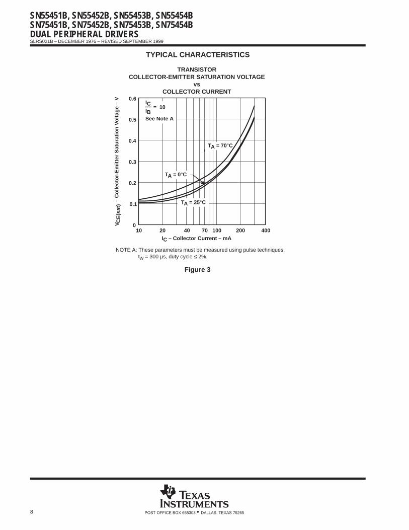
SN55451B, SN55452B, SN55453B, SN55454BSN75451B, SN75452B, SN75453B, SN75454BDUAL PERIPHERAL DRIVERS
SLRS021B – DECEMBER 1976 – REVISED SEPTEMBER 1999
8 POST OFFICE BOX 655303 • DALLAS, TEXAS 75265
TYPICAL CHARACTERISTICS
IC – Collector Current – mA
TRANSISTORCOLLECTOR-EMITTER SATURATION VOLTAGE
vsCOLLECTOR CURRENT
VC
E(s
at)
– C
olle
ctor
-Em
itter
Sat
urat
ion
Vol
tage
– V
10
0.6
4000
0.1
0.2
0.3
0.4
0.5
20 40 70 100 200
ICIB
CE
(sat
)V
= 10
TA = 25°C
TA = 0°C
TA = 70°C
See Note A
Figure 3
NOTE A: These parameters must be measured using pulse techniques, tw = 300 µs, duty cycle ≤ 2%.
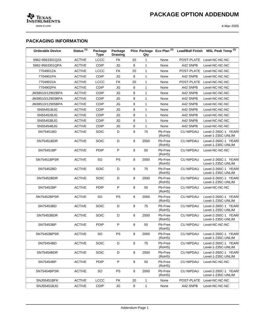
PACKAGING INFORMATION
Orderable Device Status (1) PackageType
PackageDrawing
Pins PackageQty
Eco Plan (2) Lead/Ball Finish MSL Peak Temp (3)
5962-9563301Q2A ACTIVE LCCC FK 20 1 None POST-PLATE Level-NC-NC-NC
5962-9563301QPA ACTIVE CDIP JG 8 1 None A42 SNPB Level-NC-NC-NC
77049012A ACTIVE LCCC FK 20 1 None POST-PLATE Level-NC-NC-NC
7704901PA ACTIVE CDIP JG 8 1 None A42 SNPB Level-NC-NC-NC
77049022A ACTIVE LCCC FK 20 1 None POST-PLATE Level-NC-NC-NC
7704902PA ACTIVE CDIP JG 8 1 None A42 SNPB Level-NC-NC-NC
JM38510/12902BPA ACTIVE CDIP JG 8 1 None A42 SNPB Level-NC-NC-NC
JM38510/12903BPA ACTIVE CDIP JG 8 1 None A42 SNPB Level-NC-NC-NC
JM38510/12905BPA ACTIVE CDIP JG 8 1 None A42 SNPB Level-NC-NC-NC
SN55451BJG ACTIVE CDIP JG 8 1 None A42 SNPB Level-NC-NC-NC
SN55452BJG ACTIVE CDIP JG 8 1 None A42 SNPB Level-NC-NC-NC
SN55453BJG ACTIVE CDIP JG 8 1 None A42 SNPB Level-NC-NC-NC
SN55454BJG ACTIVE CDIP JG 8 1 None A42 SNPB Level-NC-NC-NC
SN75451BD ACTIVE SOIC D 8 75 Pb-Free(RoHS)
CU NIPDAU Level-2-260C-1 YEAR/Level-1-235C-UNLIM
SN75451BDR ACTIVE SOIC D 8 2500 Pb-Free(RoHS)
CU NIPDAU Level-2-260C-1 YEAR/Level-1-235C-UNLIM
SN75451BP ACTIVE PDIP P 8 50 Pb-Free(RoHS)
CU NIPDAU Level-NC-NC-NC
SN75451BPSR ACTIVE SO PS 8 2000 Pb-Free(RoHS)
CU NIPDAU Level-2-260C-1 YEAR/Level-1-235C-UNLIM
SN75452BD ACTIVE SOIC D 8 75 Pb-Free(RoHS)
CU NIPDAU Level-2-260C-1 YEAR/Level-1-235C-UNLIM
SN75452BDR ACTIVE SOIC D 8 2500 Pb-Free(RoHS)
CU NIPDAU Level-2-260C-1 YEAR/Level-1-235C-UNLIM
SN75452BP ACTIVE PDIP P 8 50 Pb-Free(RoHS)
CU NIPDAU Level-NC-NC-NC
SN75452BPSR ACTIVE SO PS 8 2000 Pb-Free(RoHS)
CU NIPDAU Level-2-260C-1 YEAR/Level-1-235C-UNLIM
SN75453BD ACTIVE SOIC D 8 75 Pb-Free(RoHS)
CU NIPDAU Level-2-260C-1 YEAR/Level-1-235C-UNLIM
SN75453BDR ACTIVE SOIC D 8 2500 Pb-Free(RoHS)
CU NIPDAU Level-2-260C-1 YEAR/Level-1-235C-UNLIM
SN75453BP ACTIVE PDIP P 8 50 Pb-Free(RoHS)
CU NIPDAU Level-NC-NC-NC
SN75453BPSR ACTIVE SO PS 8 2000 Pb-Free(RoHS)
CU NIPDAU Level-2-260C-1 YEAR/Level-1-235C-UNLIM
SN75454BD ACTIVE SOIC D 8 75 Pb-Free(RoHS)
CU NIPDAU Level-2-260C-1 YEAR/Level-1-235C-UNLIM
SN75454BDR ACTIVE SOIC D 8 2500 Pb-Free(RoHS)
CU NIPDAU Level-2-260C-1 YEAR/Level-1-235C-UNLIM
SN75454BP ACTIVE PDIP P 8 50 Pb-Free(RoHS)
CU NIPDAU Level-NC-NC-NC
SN75454BPSR ACTIVE SO PS 8 2000 Pb-Free(RoHS)
CU NIPDAU Level-2-260C-1 YEAR/Level-1-235C-UNLIM
SNJ55451BFK ACTIVE LCCC FK 20 1 None POST-PLATE Level-NC-NC-NC
SNJ55451BJG ACTIVE CDIP JG 8 1 None A42 SNPB Level-NC-NC-NC
PACKAGE OPTION ADDENDUM
www.ti.com 4-Mar-2005
Addendum-Page 1
Orderable Device Status (1) PackageType
PackageDrawing
Pins PackageQty
Eco Plan (2) Lead/Ball Finish MSL Peak Temp (3)
SNJ55452BFK ACTIVE LCCC FK 20 1 None POST-PLATE Level-NC-NC-NC
SNJ55452BJG ACTIVE CDIP JG 8 1 None A42 SNPB Level-NC-NC-NC
SNJ55453BFK ACTIVE LCCC FK 20 1 None POST-PLATE Level-NC-NC-NC
SNJ55453BJG ACTIVE CDIP JG 8 1 None A42 SNPB Level-NC-NC-NC
SNJ55454BFK OBSOLETE LCCC FK 20 None POST-PLATE Level-NC-NC-NC
SNJ55454BJG ACTIVE CDIP JG 8 1 None A42 SNPB Level-NC-NC-NC
(1) The marketing status values are defined as follows:ACTIVE: Product device recommended for new designs.LIFEBUY: TI has announced that the device will be discontinued, and a lifetime-buy period is in effect.NRND: Not recommended for new designs. Device is in production to support existing customers, but TI does not recommend using this part ina new design.PREVIEW: Device has been announced but is not in production. Samples may or may not be available.OBSOLETE: TI has discontinued the production of the device.
(2) Eco Plan - May not be currently available - please check http://www.ti.com/productcontent for the latest availability information and additionalproduct content details.None: Not yet available Lead (Pb-Free).Pb-Free (RoHS): TI's terms "Lead-Free" or "Pb-Free" mean semiconductor products that are compatible with the current RoHS requirementsfor all 6 substances, including the requirement that lead not exceed 0.1% by weight in homogeneous materials. Where designed to be solderedat high temperatures, TI Pb-Free products are suitable for use in specified lead-free processes.Green (RoHS & no Sb/Br): TI defines "Green" to mean "Pb-Free" and in addition, uses package materials that do not contain halogens,including bromine (Br) or antimony (Sb) above 0.1% of total product weight.
(3) MSL, Peak Temp. -- The Moisture Sensitivity Level rating according to the JEDECindustry standard classifications, and peak soldertemperature.
Important Information and Disclaimer:The information provided on this page represents TI's knowledge and belief as of the date that it isprovided. TI bases its knowledge and belief on information provided by third parties, and makes no representation or warranty as to theaccuracy of such information. Efforts are underway to better integrate information from third parties. TI has taken and continues to takereasonable steps to provide representative and accurate information but may not have conducted destructive testing or chemical analysis onincoming materials and chemicals. TI and TI suppliers consider certain information to be proprietary, and thus CAS numbers and other limitedinformation may not be available for release.
In no event shall TI's liability arising out of such information exceed the total purchase price of the TI part(s) at issue in this document sold by TIto Customer on an annual basis.
PACKAGE OPTION ADDENDUM
www.ti.com 4-Mar-2005
Addendum-Page 2

IMPORTANT NOTICE
Texas Instruments Incorporated and its subsidiaries (TI) reserve the right to make corrections, modifications,enhancements, improvements, and other changes to its products and services at any time and to discontinueany product or service without notice. Customers should obtain the latest relevant information before placingorders and should verify that such information is current and complete. All products are sold subject to TI’s termsand conditions of sale supplied at the time of order acknowledgment.
TI warrants performance of its hardware products to the specifications applicable at the time of sale inaccordance with TI’s standard warranty. Testing and other quality control techniques are used to the extent TIdeems necessary to support this warranty. Except where mandated by government requirements, testing of allparameters of each product is not necessarily performed.
TI assumes no liability for applications assistance or customer product design. Customers are responsible fortheir products and applications using TI components. To minimize the risks associated with customer productsand applications, customers should provide adequate design and operating safeguards.
TI does not warrant or represent that any license, either express or implied, is granted under any TI patent right,copyright, mask work right, or other TI intellectual property right relating to any combination, machine, or processin which TI products or services are used. Information published by TI regarding third-party products or servicesdoes not constitute a license from TI to use such products or services or a warranty or endorsement thereof.Use of such information may require a license from a third party under the patents or other intellectual propertyof the third party, or a license from TI under the patents or other intellectual property of TI.
Reproduction of information in TI data books or data sheets is permissible only if reproduction is withoutalteration and is accompanied by all associated warranties, conditions, limitations, and notices. Reproductionof this information with alteration is an unfair and deceptive business practice. TI is not responsible or liable forsuch altered documentation.
Resale of TI products or services with statements different from or beyond the parameters stated by TI for thatproduct or service voids all express and any implied warranties for the associated TI product or service andis an unfair and deceptive business practice. TI is not responsible or liable for any such statements.
Following are URLs where you can obtain information on other Texas Instruments products and applicationsolutions:
Products Applications
Amplifiers amplifier.ti.com Audio www.ti.com/audio
Data Converters dataconverter.ti.com Automotive www.ti.com/automotive
DSP dsp.ti.com Broadband www.ti.com/broadband
Interface interface.ti.com Digital Control www.ti.com/digitalcontrol
Logic logic.ti.com Military www.ti.com/military
Power Mgmt power.ti.com Optical Networking www.ti.com/opticalnetwork
Microcontrollers microcontroller.ti.com Security www.ti.com/security
Telephony www.ti.com/telephony
Video & Imaging www.ti.com/video
Wireless www.ti.com/wireless
Mailing Address: Texas Instruments
Post Office Box 655303 Dallas, Texas 75265
Copyright 2005, Texas Instruments Incorporated

This datasheet has been download from:
www.datasheetcatalog.com
Datasheets for electronics components.
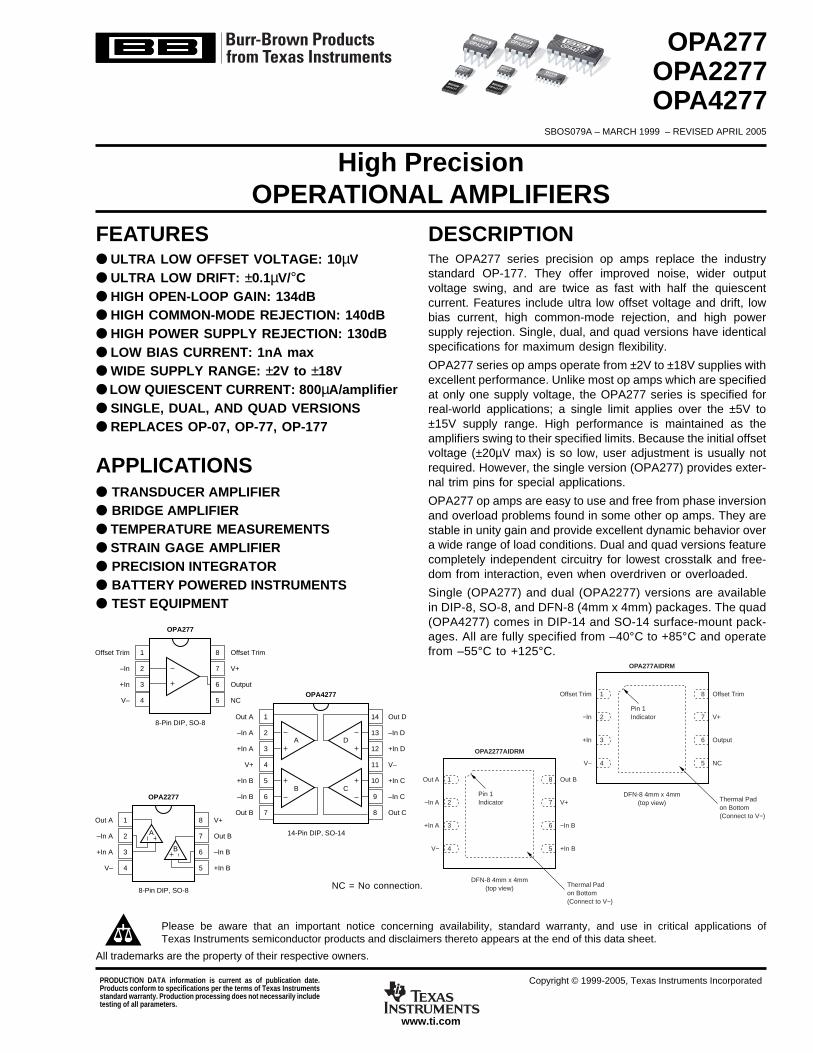
High PrecisionOPERATIONAL AMPLIFIERS
OPA277OPA2277OPA4277
SBOS079A – MARCH 1999 – REVISED APRIL 2005
www.ti.com
PRODUCTION DATA information is current as of publication date.Products conform to specifications per the terms of Texas Instrumentsstandard warranty. Production processing does not necessarily includetesting of all parameters.
Copyright © 1999-2005, Texas Instruments Incorporated
Please be aware that an important notice concerning availability, standard warranty, and use in critical applications ofTexas Instruments semiconductor products and disclaimers thereto appears at the end of this data sheet.
All trademarks are the property of their respective owners.
DESCRIPTIONThe OPA277 series precision op amps replace the industrystandard OP-177. They offer improved noise, wider outputvoltage swing, and are twice as fast with half the quiescentcurrent. Features include ultra low offset voltage and drift, lowbias current, high common-mode rejection, and high powersupply rejection. Single, dual, and quad versions have identicalspecifications for maximum design flexibility.
OPA277 series op amps operate from ±2V to ±18V supplies withexcellent performance. Unlike most op amps which are specifiedat only one supply voltage, the OPA277 series is specified forreal-world applications; a single limit applies over the ±5V to±15V supply range. High performance is maintained as theamplifiers swing to their specified limits. Because the initial offsetvoltage (±20µV max) is so low, user adjustment is usually notrequired. However, the single version (OPA277) provides exter-nal trim pins for special applications.
OPA277 op amps are easy to use and free from phase inversionand overload problems found in some other op amps. They arestable in unity gain and provide excellent dynamic behavior overa wide range of load conditions. Dual and quad versions featurecompletely independent circuitry for lowest crosstalk and free-dom from interaction, even when overdriven or overloaded.
Single (OPA277) and dual (OPA2277) versions are availablein DIP-8, SO-8, and DFN-8 (4mm x 4mm) packages. The quad(OPA4277) comes in DIP-14 and SO-14 surface-mount pack-ages. All are fully specified from –40°C to +85°C and operatefrom –55°C to +125°C.
FEATURES ULTRA LOW OFFSET VOLTAGE: 10µV ULTRA LOW DRIFT: ±0.1µV/°C HIGH OPEN-LOOP GAIN: 134dB HIGH COMMON-MODE REJECTION: 140dB HIGH POWER SUPPLY REJECTION: 130dB LOW BIAS CURRENT: 1nA max WIDE SUPPLY RANGE: ±2V to ±18V LOW QUIESCENT CURRENT: 800µA/amplifier SINGLE, DUAL, AND QUAD VERSIONS REPLACES OP-07, OP-77, OP-177
1
2
3
4
5
6
7
14
13
12
11
10
9
8
Out D
–In D
+In D
V–
+In C
–In C
Out C
Out A
–In A
+In A
V+
+In B
–In B
Out B
OPA4277
14-Pin DIP, SO-14
A D
B C
1
2
3
4
8
7
6
5
V+
Out B
–In B
+In B
Out A
–In A
+In A
V–
OPA2277
8-Pin DIP, SO-8
A
B
APPLICATIONS TRANSDUCER AMPLIFIER BRIDGE AMPLIFIER TEMPERATURE MEASUREMENTS STRAIN GAGE AMPLIFIER PRECISION INTEGRATOR BATTERY POWERED INSTRUMENTS TEST EQUIPMENT
1
2
3
4
8
7
6
5
Offset Trim
V+
Output
NC
Offset Trim
–In
+In
V–
OPA277
8-Pin DIP, SO-8
1
2
3
4
Offset Trim
−In
+In
V−
8
7
6
5
Offset Trim
Pin 1Indicator
OPA277AIDRM
DFN-8 4mm x 4mm(top view)
V+
Output
Thermal Padon Bottom(Connect to V−)
NC
1
2
3
4
Out A
−In A
+In A
V−
8
7
6
5
Out B
Pin 1Indicator
OPA2277AIDRM
DFN-8 4mm x 4mm(top view)
V+
−In B
Thermal Padon Bottom(Connect to V−)
+In B
OPA277OPA2277
OPA277OPA2277
OPA4277
OPA4277
OPA2277OPA277
NC = No connection.
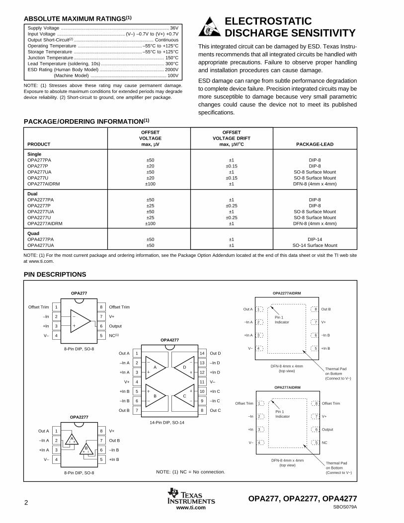
OPA277, OPA2277, OPA42772SBOS079Awww.ti.com
OFFSET OFFSETVOLTAGE VOLTAGE DRIFT
PRODUCT max, µV max, µV/°C PACKAGE-LEAD
SingleOPA277PA ±50 ±1 DIP-8OPA277P ±20 ±0.15 DIP-8OPA277UA ±50 ±1 SO-8 Surface MountOPA277U ±20 ±0.15 SO-8 Surface MountOPA277AIDRM ±100 ±1 DFN-8 (4mm x 4mm)
DualOPA2277PA ±50 ±1 DIP-8OPA2277P ±25 ±0.25 DIP-8OPA2277UA ±50 ±1 SO-8 Surface MountOPA2277U ±25 ±0.25 SO-8 Surface MountOPA2277AIDRM ±100 ±1 DFN-8 (4mm x 4mm)
QuadOPA4277PA ±50 ±1 DIP-14OPA4277UA ±50 ±1 SO-14 Surface Mount
NOTE: (1) For the most current package and ordering information, see the Package Option Addendum located at the end of this data sheet or visit the TI web siteat www.ti.com.
ABSOLUTE MAXIMUM RATINGS(1)
Supply Voltage .................................................................................... 36VInput Voltage ..................................................... (V–) –0.7V to (V+) +0.7VOutput Short-Circuit(2) .............................................................. ContinuousOperating Temperature .................................................. –55°C to +125°CStorage Temperature ..................................................... –55°C to +125°CJunction Temperature ...................................................................... 150°CLead Temperature (soldering, 10s) ................................................. 300°CESD Rating (Human Body Model) .................................................. 2000V
(Machine Model) ........................................................... 100V
NOTE: (1) Stresses above these rating may cause permanent damage.Exposure to absolute maximum conditions for extended periods may degradedevice reliability. (2) Short-circuit to ground, one amplifier per package.
PACKAGE/ORDERING INFORMATION(1)
PIN DESCRIPTIONS
ELECTROSTATICDISCHARGE SENSITIVITY
This integrated circuit can be damaged by ESD. Texas Instru-ments recommends that all integrated circuits be handled withappropriate precautions. Failure to observe proper handlingand installation procedures can cause damage.
ESD damage can range from subtle performance degradationto complete device failure. Precision integrated circuits may bemore susceptible to damage because very small parametricchanges could cause the device not to meet its publishedspecifications.
1
2
3
4
5
6
7
14
13
12
11
10
9
8
Out D
–In D
+In D
V–
+In C
–In C
Out C
Out A
–In A
+In A
V+
+In B
–In B
Out B
OPA4277
14-Pin DIP, SO-14
A D
B C
1
2
3
4
8
7
6
5
V+
Out B
–In B
+In B
Out A
–In A
+In A
V–
OPA2277
8-Pin DIP, SO-8
A
B
1
2
3
4
8
7
6
5
Offset Trim
V+
Output
NC(1)
Offset Trim
–In
+In
V–
OPA277
8-Pin DIP, SO-8
1
2
3
4
Out A
−In A
+In A
V−
8
7
6
5
Out B
Pin 1Indicator
OPA2277AIDRM
DFN-8 4mm x 4mm(top view)
V+
−In B
Thermal Padon Bottom(Connect to V−)
+In B
1
2
3
4
Offset Trim
−In
+In
V−
8
7
6
5
Offset Trim
Pin 1Indicator
OPA277AIDRM
DFN-8 4mm x 4mm(top view)
V+
Output
Thermal Padon Bottom(Connect to V−)
NC
NOTE: (1) NC = No connection.
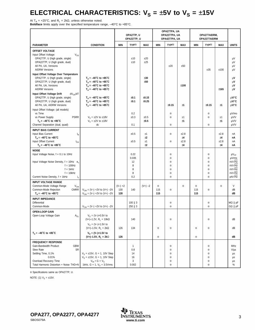
OPA277, OPA2277, OPA4277 3SBOS079A www.ti.com
ELECTRICAL CHARACTERISTICS: VS = ±5V to VS = ±15VAt TA = +25°C, and RL = 2kΩ, unless otherwise noted.Boldface limits apply over the specified temperature range, –40°C to +85°C.
OPA277PA, UAOPA277P, U OPA2277PA, UA OPA277AIDRM,OPA2277P, U OPA4277PA, UA OPA2277AIDRM
PARAMETER CONDITION MIN TYP(1) MAX MIN TYP(1) MAX MIN TYP(1) MAX UNITS
OFFSET VOLTAGEInput Offset Voltage: VOS
OPA277P, U (high grade, single) ±10 ±20 µVOPA2277P, U (high grade, dual) ±10 ±25 µVAll PA, UA, Versions ±20 ±50 µVAIDRM Versions ±35 ±100 µV
Input Offset Voltage Over TemperatureOPA277P, U (high grade, single) TA = –40°C to +85°C ±30 µVOPA2277P, U (high grade, dual) TA = –40°C to +85°C ±50 µVAll PA, UA, Versions TA = –40°C to +85°C ±100 µVAIDRM Versions TA = –40°C to +85°C ±165 µV
Input Offset Voltage Drift dVOS/dTOPA277P, U (high grade, single) TA = –40°C to +85°C ±0.1 ±0.15 µV/°COPA2277P, U (high grade, dual) TA = –40°C to +85°C ±0.1 ±0.25 µV/°CAll PA, UA, AIDRM Versions TA = –40°C to +85°C ±0.15 ±1 ±0.15 ±1 µV/°C
Input Offset Voltage: (all models)vs Time 0.2 µV/movs Power Supply PSRR VS = ±2V to ±18V ±0.3 ±0.5 ±1 ±1 µV/V
TA = –40°C to +85°C VS = ±2V to ±18V ±0.5 ±1 ±1 µV/VChannel Separation (dual, quad) dc 0.1 µV/V
INPUT BIAS CURRENTInput Bias Current IB ±0.5 ±1 ±2.8 ±2.8 nA
TA = –40°C to +85°C ±2 ±4 ±4 nAInput Offset Current IOS ±0.5 ±1 ±2.8 ±2.8 nA
TA = –40°C to +85°C ±2 ±4 ±4 nA
NOISEInput Voltage Noise, f = 0.1 to 10Hz 0.22 µVPP
0.035 µVrmsInput Voltage Noise Density, f = 10Hz en 12 nV/√Hz
f = 100Hz 8 nV/√Hzf = 1kHz 8 nV/√Hzf = 10kHz 8 nV/√Hz
Current Noise Density, f = 1kHz in 0.2 pA/√Hz
INPUT VOLTAGE RANGECommon-Mode Voltage Range VCM (V–) +2 (V+) –2 VCommon-Mode Rejection CMRR VCM = (V–) +2V to (V+) –2V 130 140 115 115 dB
TA = –40°C to +85°C VCM = (V–) +2V to (V+) –2V 128 115 115 dB
INPUT IMPEDANCEDifferential 100 || 3 MΩ || pFCommon-Mode VCM = (V–) +2V to (V+) –2V 250 || 3 GΩ || pF
OPEN-LOOP GAINOpen-Loop Voltage Gain AOL VO = (V–)+0.5V to
(V+)–1.2V, RL = 10kΩ 140 dB
VO = (V–)+1.5V to(V+)–1.5V, RL = 2kΩ 126 134 dB
TA = –40°C to +85°C VO = (V–)+1.5V to(V+)–1.5V, RL = 2kΩ 126 dB
FREQUENCY RESPONSEGain-Bandwidth Product GBW 1 MHzSlew Rate SR 0.8 V/µsSettling Time, 0.1% VS = ±15V, G = 1, 10V Step 14 µs
0.01% VS = ±15V, G = 1, 10V Step 16 µsOverload Recovery Time VIN • G = VS 3 µsTotal Harmonic Distortion + Noise THD+N 1kHz, G = 1, VO = 3.5Vrms 0.002 %
Specifications same as OPA277P, U.
NOTE: (1) VS = ±15V.
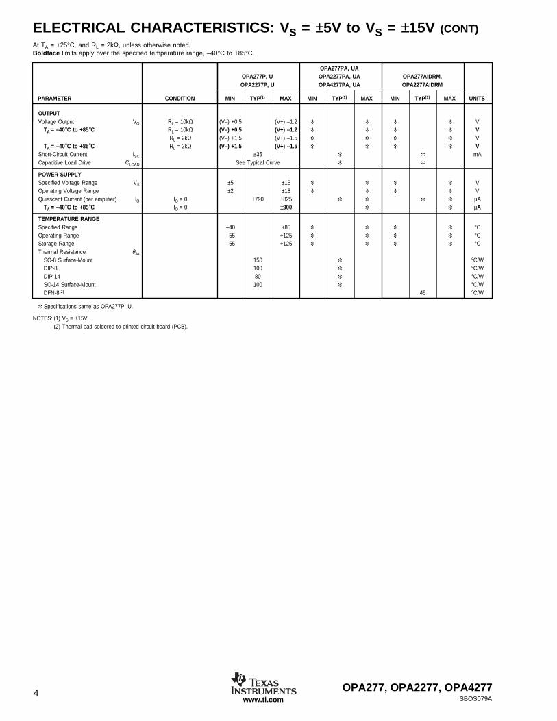
OPA277, OPA2277, OPA42774SBOS079Awww.ti.com
ELECTRICAL CHARACTERISTICS: VS = ±5V to VS = ±15V (CONT)At TA = +25°C, and RL = 2kΩ, unless otherwise noted.Boldface limits apply over the specified temperature range, –40°C to +85°C.
OPA277PA, UAOPA277P, U OPA2277PA, UA OPA277AIDRM,OPA2277P, U OPA4277PA, UA OPA2277AIDRM
PARAMETER CONDITION MIN TYP(1) MAX MIN TYP(1) MAX MIN TYP(1) MAX UNITS
OUTPUTVoltage Output VO RL = 10kΩ (V–) +0.5 (V+) –1.2 V
TA = –40°C to +85°C RL = 10kΩ (V–) +0.5 (V+) –1.2 VRL = 2kΩ (V–) +1.5 (V+) –1.5 V
TA = –40°C to +85°C RL = 2kΩ (V–) +1.5 (V+) –1.5 VShort-Circuit Current ISC ±35 mACapacitive Load Drive CLOAD See Typical Curve
POWER SUPPLYSpecified Voltage Range VS ±5 ±15 VOperating Voltage Range ±2 ±18 VQuiescent Current (per amplifier) IQ IO = 0 ±790 ±825 µA
TA = –40°C to +85°C IO = 0 ±900 µA
TEMPERATURE RANGESpecified Range –40 +85 °COperating Range –55 +125 °CStorage Range –55 +125 °CThermal Resistance θJA
SO-8 Surface-Mount 150 °C/WDIP-8 100 °C/WDIP-14 80 °C/WSO-14 Surface-Mount 100 °C/WDFN-8(2) 45 °C/W
Specifications same as OPA277P, U.
NOTES: (1) VS = ±15V.(2) Thermal pad soldered to printed circuit board (PCB).
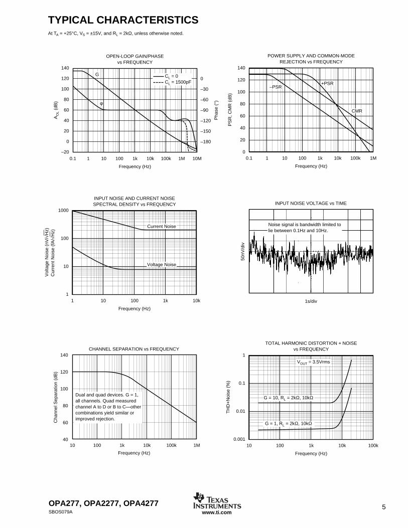
OPA277, OPA2277, OPA4277 5SBOS079A www.ti.com
TYPICAL CHARACTERISTICSAt TA = +25°C, VS = ±15V, and RL = 2kΩ, unless otherwise noted.
10 100 1k 10k 100k
Frequency (Hz)
CHANNEL SEPARATION vs FREQUENCY
1M
140
120
100
80
60
40
Cha
nnel
Sep
arat
ion
(dB
)
Dual and quad devices. G = 1, all channels. Quad measured channel A to D or B to C—other combinations yield similar or improved rejection.
10 100 1k 10k 100k
1
0.1
0.01
0.001
TH
D+
Noi
se (
%)
Frequency (Hz)
TOTAL HARMONIC DISTORTION + NOISEvs FREQUENCY
VOUT = 3.5Vrms
G = 10, RL = 2kΩ, 10kΩ
G = 1, RL = 2kΩ, 10kΩ
1 10 100 1k 10k
1000
100
10
1
Vol
tage
Noi
se (
nV/√
Hz)
Cur
rent
Noi
se (
fA/√
Hz)
Frequency (Hz)
INPUT NOISE AND CURRENT NOISESPECTRAL DENSITY vs FREQUENCY
Current Noise
Voltage Noise
0.1 1 10 100 1k 10k 100k 1M 10M
140
120
100
80
60
40
20
0
–20
AO
L (d
B)
0
–30
–60
–90
–120
–150
–180
Pha
se (
°)
Frequency (Hz)
OPEN-LOOP GAIN/PHASEvs FREQUENCY
G
φ
CL = 0CL = 1500pF
0.1 1 10 100 1k 10k 100k 1M
140
120
100
80
60
40
20
0
PS
R, C
MR
(dB
)
Frequency (Hz)
POWER SUPPLY AND COMMON-MODEREJECTION vs FREQUENCY
+PSR
CMR
–PSR
1s/div
INPUT NOISE VOLTAGE vs TIME
50nV
/div
Noise signal is bandwidth limited to lie between 0.1Hz and 10Hz.
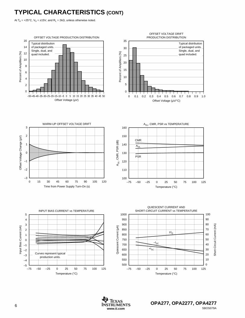
OPA277, OPA2277, OPA42776SBOS079Awww.ti.com
TYPICAL CHARACTERISTICS (CONT)At TA = +25°C, VS = ±15V, and RL = 2kΩ, unless otherwise noted.
OFFSET VOLTAGE PRODUCTION DISTRIBUTION
Per
cent
of A
mpl
ifier
s (%
)
Offset Voltage (µV)–50–45–40–35–30–25–20–15–10 –5 0 5 10 15 20 25 30 35 40 45 50
16
14
12
10
8
6
4
2
0
Typical distributionof packaged units.Single, dual, andquad included.
3
2
1
0
–1
–2
–3
Offs
et V
olta
ge C
hang
e (µ
V)
0 30 60 90 120
Time from Power Supply Turn-On (s)
WARM-UP OFFSET VOLTAGE DRIFT
15 45 75 105
OFFSET VOLTAGE DRIFTPRODUCTION DISTRIBUTION
Per
cent
of A
mpl
ifier
s (%
)
Offset Voltage (µV/°C)
0 0.1 0.2 0.3 0.4 0.5 0.6 0.7 0.8 0.9 1.0
35
30
25
20
15
10
5
0
Typical distributionof packaged units.Single, dual, andquad included.
INPUT BIAS CURRENT vs TEMPERATURE
125
Temperature (°C)
–75 –50 –25 0 25 50 75 100
5
4
3
2
1
0
–1
–2
–3
–4
–5
Inpu
t Bia
s C
urre
nt (
nA)
Curves represent typicalproduction units.
–75 –50 –25 0 25 50 75 100 125
160
150
140
130
120
110
100
AO
L, C
MR
, PS
R (
dB)
Temperature (°C)
AOL, CMR, PSR vs TEMPERATURE
CMR
AOL
PSR
–75 –50 –25 0 25 50 75 100 125
1000
950
900
850
800
750
700
650
600
550
500
Qui
esce
nt C
urre
nt (
µA)
100
90
80
70
60
50
40
30
20
10
0
Sho
rt-C
ircui
t Cur
rent
(m
A)
Temperature (°C)
QUIESCENT CURRENT ANDSHORT-CIRCUIT CURRENT vs TEMPERATURE
+ISC
–ISC
±IQ
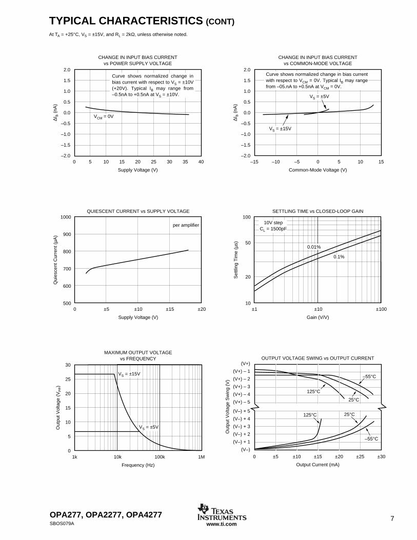
OPA277, OPA2277, OPA4277 7SBOS079A www.ti.com
TYPICAL CHARACTERISTICS (CONT)At TA = +25°C, VS = ±15V, and RL = 2kΩ, unless otherwise noted.
CHANGE IN INPUT BIAS CURRENTvs POWER SUPPLY VOLTAGE
40
Supply Voltage (V)
0 5 10 15 20 25 30 35
2.0
1.5
1.0
0.5
0.0
–0.5
–1.0
–1.5
–2.0
∆IB (
nA)
Curve shows normalized change in bias current with respect to VS = ±10V (+20V). Typical IB may range from –0.5nA to +0.5nA at VS = ±10V.
VCM = 0V
CHANGE IN INPUT BIAS CURRENTvs COMMON-MODE VOLTAGE
15
Common-Mode Voltage (V)
–15 –10 –5 0 5 10
2.0
1.5
1.0
0.5
0.0
–0.5
–1.0
–1.5
–2.0
∆IB (
nA)
VS = ±5V
VS = ±15V
Curve shows normalized change in bias current with respect to VCM = 0V. Typical IB may range from –05.nA to +0.5nA at VCM = 0V.
OUTPUT VOLTAGE SWING vs OUTPUT CURRENT(V+)
(V+) – 1
(V+) – 2
(V+) – 3
(V+) – 4
(V+) – 5
(V–) + 5
(V–) + 4
(V–) + 3
(V–) + 2
(V–) + 1
(V–)
0 ±5 ±10 ±15 ±20 ±25 ±30
Output Current (mA)
Out
put V
olta
ge S
win
g (V
)
–55°C
–55°C
125°C
25°C
125°C 25°C
1000
900
800
700
600
500
Qui
esce
nt C
urre
nt (
µA)
0 ±5 ±10 ±15 ±20
Supply Voltage (V)
QUIESCENT CURRENT vs SUPPLY VOLTAGE
per amplifier
100
10
20
50
Set
tling
Tim
e (µ
s)
±1 ±10 ±100
Gain (V/V)
SETTLING TIME vs CLOSED-LOOP GAIN
0.01%
10V stepCL = 1500pF
0.1%
MAXIMUM OUTPUT VOLTAGEvs FREQUENCY
1M
Frequency (Hz)
1k 10k 100k
30
25
20
15
10
5
0
Out
put V
olta
ge (
VP
P)
VS = ±15V
VS = ±5V
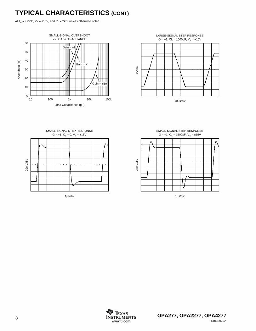
OPA277, OPA2277, OPA42778SBOS079Awww.ti.com
TYPICAL CHARACTERISTICS (CONT)At TA = +25°C, VS = ±15V, and RL = 2kΩ, unless otherwise noted.
SMALL-SIGNAL OVERSHOOTvs LOAD CAPACITANCE
1k10010 10k 100k
Load Capacitance (pF)
60
50
40
30
20
10
0
Ove
rsho
ot (
%)
Gain = –1
Gain = +1
Gain = ±10
10µs/div
LARGE-SIGNAL STEP RESPONSEG = +1, CL = 1500pF, VS = +15V
2V/d
iv
1µs/div
SMALL-SIGNAL STEP RESPONSEG = +1, CL = 0, VS = ±15V
20m
V/d
iv
1µs/div
SMALL-SIGNAL STEP RESPONSEG = +1, CL = 1500pF, VS = ±15V20
mV
/div
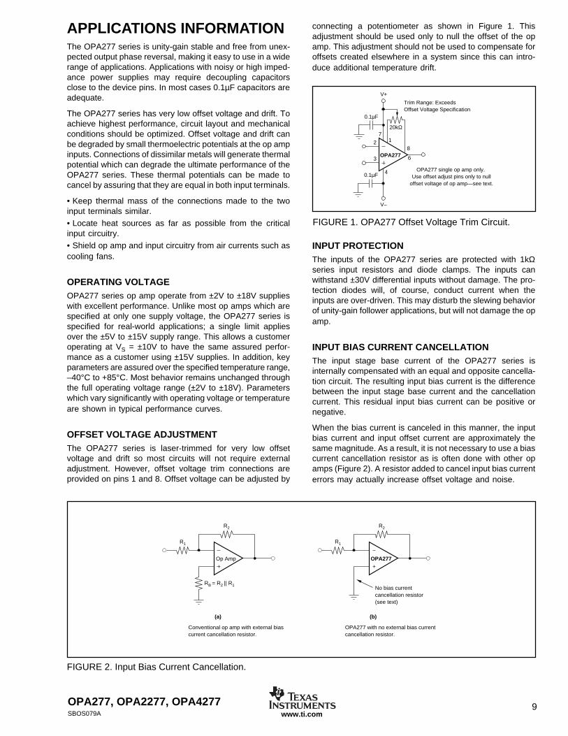
OPA277, OPA2277, OPA4277 9SBOS079A www.ti.com
Op Amp
(a)
OPA277
(b)
No bias currentcancellation resistor(see text)
Conventional op amp with external biascurrent cancellation resistor.
OPA277 with no external bias currentcancellation resistor.
R2
R1
R2
R1
RB = R2 || R1
APPLICATIONS INFORMATIONThe OPA277 series is unity-gain stable and free from unex-pected output phase reversal, making it easy to use in a widerange of applications. Applications with noisy or high imped-ance power supplies may require decoupling capacitorsclose to the device pins. In most cases 0.1µF capacitors areadequate.
The OPA277 series has very low offset voltage and drift. Toachieve highest performance, circuit layout and mechanicalconditions should be optimized. Offset voltage and drift canbe degraded by small thermoelectric potentials at the op ampinputs. Connections of dissimilar metals will generate thermalpotential which can degrade the ultimate performance of theOPA277 series. These thermal potentials can be made tocancel by assuring that they are equal in both input terminals.
• Keep thermal mass of the connections made to the twoinput terminals similar.• Locate heat sources as far as possible from the criticalinput circuitry.• Shield op amp and input circuitry from air currents such ascooling fans.
OPERATING VOLTAGEOPA277 series op amp operate from ±2V to ±18V supplieswith excellent performance. Unlike most op amps which arespecified at only one supply voltage, the OPA277 series isspecified for real-world applications; a single limit appliesover the ±5V to ±15V supply range. This allows a customeroperating at VS = ±10V to have the same assured perfor-mance as a customer using ±15V supplies. In addition, keyparameters are assured over the specified temperature range,–40°C to +85°C. Most behavior remains unchanged throughthe full operating voltage range (±2V to ±18V). Parameterswhich vary significantly with operating voltage or temperatureare shown in typical performance curves.
OFFSET VOLTAGE ADJUSTMENTThe OPA277 series is laser-trimmed for very low offsetvoltage and drift so most circuits will not require externaladjustment. However, offset voltage trim connections areprovided on pins 1 and 8. Offset voltage can be adjusted by
connecting a potentiometer as shown in Figure 1. Thisadjustment should be used only to null the offset of the opamp. This adjustment should not be used to compensate foroffsets created elsewhere in a system since this can intro-duce additional temperature drift.
INPUT PROTECTIONThe inputs of the OPA277 series are protected with 1kΩseries input resistors and diode clamps. The inputs canwithstand ±30V differential inputs without damage. The pro-tection diodes will, of course, conduct current when theinputs are over-driven. This may disturb the slewing behaviorof unity-gain follower applications, but will not damage the opamp.
INPUT BIAS CURRENT CANCELLATIONThe input stage base current of the OPA277 series isinternally compensated with an equal and opposite cancella-tion circuit. The resulting input bias current is the differencebetween the input stage base current and the cancellationcurrent. This residual input bias current can be positive ornegative.
When the bias current is canceled in this manner, the inputbias current and input offset current are approximately thesame magnitude. As a result, it is not necessary to use a biascurrent cancellation resistor as is often done with other opamps (Figure 2). A resistor added to cancel input bias currenterrors may actually increase offset voltage and noise.
FIGURE 2. Input Bias Current Cancellation.
V+
V–
20kΩ
OPA277 single op amp only. Use offset adjust pins only to null
offset voltage of op amp—see text.
Trim Range: ExceedsOffset Voltage Specification
OPA277 6
7
8
4
3
2 1
0.1µF
0.1µF
FIGURE 1. OPA277 Offset Voltage Trim Circuit.
OPA277, OPA2277, OPA427710SBOS079Awww.ti.com
R1
V–
1/2OPA2277
R2
1/2OPA2277 VOUT = (V1 – V2)(1 + )
R2
R1
V+
V+
V–
R2
For integrated solution see: INA126, INA2126 (dual)INA125 (on-board reference)INA122 (single-supply)
R1
LoadCell
R+∆RV2
R–∆R
R–∆RR+∆R
V1
141
12
5V
1113
IREG ∼ 1mA
4
3
2
6
RG1250Ω XTR105
1/2OPA2277
7
RG
RG
VIN–
VIN+
VREG
IR2
V+
IRET
IO
E
B
8
IO = 4mA + (VIN – VIN)+ – 40RG
9
10
RF10kΩ
R412Ω
1/2OPA2277
V+
V–
Type J
25Ω
(G = 1 + = 50)2RF
R
50Ω
1kΩ
RF10kΩ
IR1
VLIN
RCM = 1250Ω
0.01µF
FIGURE 3. Load Cell Amplifier.
FIGURE 4. Thermocouple Low Offset, Low Drift Loop Measurement with Diode Cold Junction Compensation.
OPA277, OPA2277, OPA4277 11SBOS079A www.ti.com
DFN PACKAGEThe OPA277 series uses the 8-lead DFN (also known asSON), which is a QFN package with contacts on only twosides of the package bottom. This leadless, near-chip-scalepackage maximizes board space and enhances thermal andelectrical characteristics through an exposed pad.
DFN packages are physically small, have a smaller routingarea, improved thermal performance, and improved electricalparasitics, with a pinout scheme that is consistent with othercommonly-used packages, such as SO and MSOP. Addition-ally, the absence of external leads eliminates bent-leadissues.
The DFN package can be easily mounted using standardprinted circuit board (PCB) assembly techniques. See Appli-cation Note, QFN/SON PCB Attachment (SLUA271) andApplication Report, Quad Flatpack No-Lead Logic Packages(SCBA017), both available for download at www.ti.com.
The exposed leadframe die pad on the bottom of thepackage should be connected to V–.
LAYOUT GUIDELINESThe leadframe die pad should be soldered to a thermal padon the PCB. Mechanical drawings located at the end of thisdata sheet list the physical dimensions for the package andpad.
Soldering the exposed pad significantly improves board-levelreliability during temperature cycling, key push, packageshear, and similar board-level tests. Even with applicationsthat have low-power dissipation, the exposed pad must besoldered to the PCB to provide structural integrity and long-term reliability.
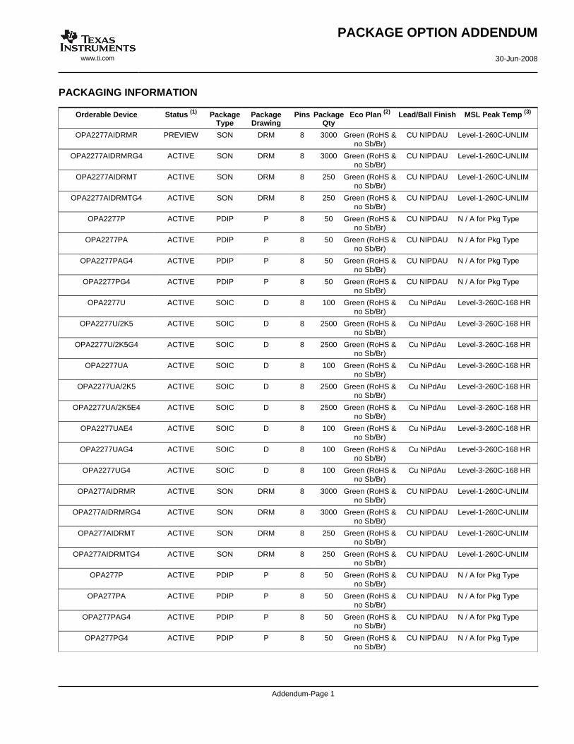
PACKAGING INFORMATION
Orderable Device Status (1) PackageType
PackageDrawing
Pins PackageQty
Eco Plan (2) Lead/Ball Finish MSL Peak Temp (3)
OPA2277AIDRMR PREVIEW SON DRM 8 3000 Green (RoHS &no Sb/Br)
CU NIPDAU Level-1-260C-UNLIM
OPA2277AIDRMRG4 ACTIVE SON DRM 8 3000 Green (RoHS &no Sb/Br)
CU NIPDAU Level-1-260C-UNLIM
OPA2277AIDRMT ACTIVE SON DRM 8 250 Green (RoHS &no Sb/Br)
CU NIPDAU Level-1-260C-UNLIM
OPA2277AIDRMTG4 ACTIVE SON DRM 8 250 Green (RoHS &no Sb/Br)
CU NIPDAU Level-1-260C-UNLIM
OPA2277P ACTIVE PDIP P 8 50 Green (RoHS &no Sb/Br)
CU NIPDAU N / A for Pkg Type
OPA2277PA ACTIVE PDIP P 8 50 Green (RoHS &no Sb/Br)
CU NIPDAU N / A for Pkg Type
OPA2277PAG4 ACTIVE PDIP P 8 50 Green (RoHS &no Sb/Br)
CU NIPDAU N / A for Pkg Type
OPA2277PG4 ACTIVE PDIP P 8 50 Green (RoHS &no Sb/Br)
CU NIPDAU N / A for Pkg Type
OPA2277U ACTIVE SOIC D 8 100 Green (RoHS &no Sb/Br)
Cu NiPdAu Level-3-260C-168 HR
OPA2277U/2K5 ACTIVE SOIC D 8 2500 Green (RoHS &no Sb/Br)
Cu NiPdAu Level-3-260C-168 HR
OPA2277U/2K5G4 ACTIVE SOIC D 8 2500 Green (RoHS &no Sb/Br)
Cu NiPdAu Level-3-260C-168 HR
OPA2277UA ACTIVE SOIC D 8 100 Green (RoHS &no Sb/Br)
Cu NiPdAu Level-3-260C-168 HR
OPA2277UA/2K5 ACTIVE SOIC D 8 2500 Green (RoHS &no Sb/Br)
Cu NiPdAu Level-3-260C-168 HR
OPA2277UA/2K5E4 ACTIVE SOIC D 8 2500 Green (RoHS &no Sb/Br)
Cu NiPdAu Level-3-260C-168 HR
OPA2277UAE4 ACTIVE SOIC D 8 100 Green (RoHS &no Sb/Br)
Cu NiPdAu Level-3-260C-168 HR
OPA2277UAG4 ACTIVE SOIC D 8 100 Green (RoHS &no Sb/Br)
Cu NiPdAu Level-3-260C-168 HR
OPA2277UG4 ACTIVE SOIC D 8 100 Green (RoHS &no Sb/Br)
Cu NiPdAu Level-3-260C-168 HR
OPA277AIDRMR ACTIVE SON DRM 8 3000 Green (RoHS &no Sb/Br)
CU NIPDAU Level-1-260C-UNLIM
OPA277AIDRMRG4 ACTIVE SON DRM 8 3000 Green (RoHS &no Sb/Br)
CU NIPDAU Level-1-260C-UNLIM
OPA277AIDRMT ACTIVE SON DRM 8 250 Green (RoHS &no Sb/Br)
CU NIPDAU Level-1-260C-UNLIM
OPA277AIDRMTG4 ACTIVE SON DRM 8 250 Green (RoHS &no Sb/Br)
CU NIPDAU Level-1-260C-UNLIM
OPA277P ACTIVE PDIP P 8 50 Green (RoHS &no Sb/Br)
CU NIPDAU N / A for Pkg Type
OPA277PA ACTIVE PDIP P 8 50 Green (RoHS &no Sb/Br)
CU NIPDAU N / A for Pkg Type
OPA277PAG4 ACTIVE PDIP P 8 50 Green (RoHS &no Sb/Br)
CU NIPDAU N / A for Pkg Type
OPA277PG4 ACTIVE PDIP P 8 50 Green (RoHS &no Sb/Br)
CU NIPDAU N / A for Pkg Type
PACKAGE OPTION ADDENDUM
www.ti.com 30-Jun-2008
Addendum-Page 1
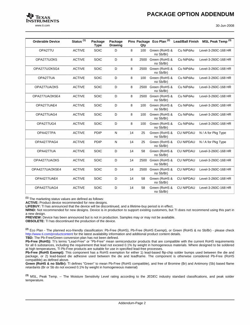
Orderable Device Status (1) PackageType
PackageDrawing
Pins PackageQty
Eco Plan (2) Lead/Ball Finish MSL Peak Temp (3)
OPA277U ACTIVE SOIC D 8 100 Green (RoHS &no Sb/Br)
Cu NiPdAu Level-3-260C-168 HR
OPA277U/2K5 ACTIVE SOIC D 8 2500 Green (RoHS &no Sb/Br)
Cu NiPdAu Level-3-260C-168 HR
OPA277U/2K5G4 ACTIVE SOIC D 8 2500 Green (RoHS &no Sb/Br)
Cu NiPdAu Level-3-260C-168 HR
OPA277UA ACTIVE SOIC D 8 100 Green (RoHS &no Sb/Br)
Cu NiPdAu Level-3-260C-168 HR
OPA277UA/2K5 ACTIVE SOIC D 8 2500 Green (RoHS &no Sb/Br)
Cu NiPdAu Level-3-260C-168 HR
OPA277UA/2K5E4 ACTIVE SOIC D 8 2500 Green (RoHS &no Sb/Br)
Cu NiPdAu Level-3-260C-168 HR
OPA277UAE4 ACTIVE SOIC D 8 100 Green (RoHS &no Sb/Br)
Cu NiPdAu Level-3-260C-168 HR
OPA277UAG4 ACTIVE SOIC D 8 100 Green (RoHS &no Sb/Br)
Cu NiPdAu Level-3-260C-168 HR
OPA277UG4 ACTIVE SOIC D 8 100 Green (RoHS &no Sb/Br)
Cu NiPdAu Level-3-260C-168 HR
OPA4277PA ACTIVE PDIP N 14 25 Green (RoHS &no Sb/Br)
CU NIPDAU N / A for Pkg Type
OPA4277PAG4 ACTIVE PDIP N 14 25 Green (RoHS &no Sb/Br)
CU NIPDAU N / A for Pkg Type
OPA4277UA ACTIVE SOIC D 14 58 Green (RoHS &no Sb/Br)
CU NIPDAU Level-3-260C-168 HR
OPA4277UA/2K5 ACTIVE SOIC D 14 2500 Green (RoHS &no Sb/Br)
CU NIPDAU Level-3-260C-168 HR
OPA4277UA/2K5E4 ACTIVE SOIC D 14 2500 Green (RoHS &no Sb/Br)
CU NIPDAU Level-3-260C-168 HR
OPA4277UAE4 ACTIVE SOIC D 14 58 Green (RoHS &no Sb/Br)
CU NIPDAU Level-3-260C-168 HR
OPA4277UAG4 ACTIVE SOIC D 14 58 Green (RoHS &no Sb/Br)
CU NIPDAU Level-3-260C-168 HR
(1) The marketing status values are defined as follows:ACTIVE: Product device recommended for new designs.LIFEBUY: TI has announced that the device will be discontinued, and a lifetime-buy period is in effect.NRND: Not recommended for new designs. Device is in production to support existing customers, but TI does not recommend using this part ina new design.PREVIEW: Device has been announced but is not in production. Samples may or may not be available.OBSOLETE: TI has discontinued the production of the device.
(2) Eco Plan - The planned eco-friendly classification: Pb-Free (RoHS), Pb-Free (RoHS Exempt), or Green (RoHS & no Sb/Br) - please checkhttp://www.ti.com/productcontent for the latest availability information and additional product content details.TBD: The Pb-Free/Green conversion plan has not been defined.Pb-Free (RoHS): TI's terms "Lead-Free" or "Pb-Free" mean semiconductor products that are compatible with the current RoHS requirementsfor all 6 substances, including the requirement that lead not exceed 0.1% by weight in homogeneous materials. Where designed to be solderedat high temperatures, TI Pb-Free products are suitable for use in specified lead-free processes.Pb-Free (RoHS Exempt): This component has a RoHS exemption for either 1) lead-based flip-chip solder bumps used between the die andpackage, or 2) lead-based die adhesive used between the die and leadframe. The component is otherwise considered Pb-Free (RoHScompatible) as defined above.Green (RoHS & no Sb/Br): TI defines "Green" to mean Pb-Free (RoHS compatible), and free of Bromine (Br) and Antimony (Sb) based flameretardants (Br or Sb do not exceed 0.1% by weight in homogeneous material)
(3) MSL, Peak Temp. -- The Moisture Sensitivity Level rating according to the JEDEC industry standard classifications, and peak soldertemperature.
PACKAGE OPTION ADDENDUM
www.ti.com 30-Jun-2008
Addendum-Page 2

Important Information and Disclaimer:The information provided on this page represents TI's knowledge and belief as of the date that it isprovided. TI bases its knowledge and belief on information provided by third parties, and makes no representation or warranty as to theaccuracy of such information. Efforts are underway to better integrate information from third parties. TI has taken and continues to takereasonable steps to provide representative and accurate information but may not have conducted destructive testing or chemical analysis onincoming materials and chemicals. TI and TI suppliers consider certain information to be proprietary, and thus CAS numbers and other limitedinformation may not be available for release.
In no event shall TI's liability arising out of such information exceed the total purchase price of the TI part(s) at issue in this document sold by TIto Customer on an annual basis.
PACKAGE OPTION ADDENDUM
www.ti.com 30-Jun-2008
Addendum-Page 3
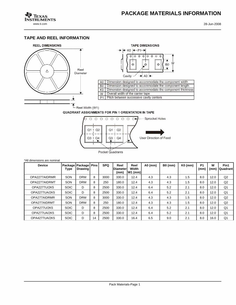
TAPE AND REEL INFORMATION
*All dimensions are nominal
Device PackageType
PackageDrawing
Pins SPQ ReelDiameter
(mm)
ReelWidth
W1 (mm)
A0 (mm) B0 (mm) K0 (mm) P1(mm)
W(mm)
Pin1Quadrant
OPA2277AIDRMR SON DRM 8 3000 330.0 12.4 4.3 4.3 1.5 8.0 12.0 Q2
OPA2277AIDRMT SON DRM 8 250 180.0 12.4 4.3 4.3 1.5 8.0 12.0 Q2
OPA2277U/2K5 SOIC D 8 2500 330.0 12.4 6.4 5.2 2.1 8.0 12.0 Q1
OPA2277UA/2K5 SOIC D 8 2500 330.0 12.4 6.4 5.2 2.1 8.0 12.0 Q1
OPA277AIDRMR SON DRM 8 3000 330.0 12.4 4.3 4.3 1.5 8.0 12.0 Q2
OPA277AIDRMT SON DRM 8 250 180.0 12.4 4.3 4.3 1.5 8.0 12.0 Q2
OPA277U/2K5 SOIC D 8 2500 330.0 12.4 6.4 5.2 2.1 8.0 12.0 Q1
OPA277UA/2K5 SOIC D 8 2500 330.0 12.4 6.4 5.2 2.1 8.0 12.0 Q1
OPA4277UA/2K5 SOIC D 14 2500 330.0 16.4 6.5 9.0 2.1 8.0 16.0 Q1
PACKAGE MATERIALS INFORMATION
www.ti.com 28-Jun-2008
Pack Materials-Page 1
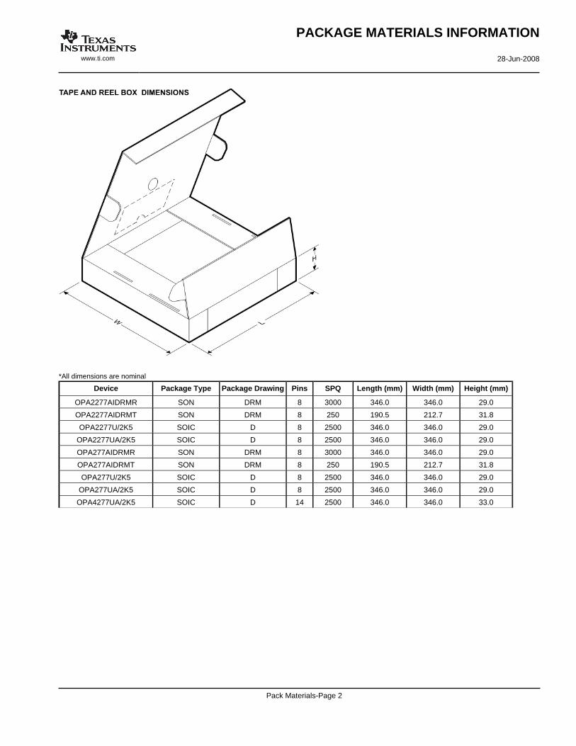
*All dimensions are nominal
Device Package Type Package Drawing Pins SPQ Length (mm) Width (mm) Height (mm)
OPA2277AIDRMR SON DRM 8 3000 346.0 346.0 29.0
OPA2277AIDRMT SON DRM 8 250 190.5 212.7 31.8
OPA2277U/2K5 SOIC D 8 2500 346.0 346.0 29.0
OPA2277UA/2K5 SOIC D 8 2500 346.0 346.0 29.0
OPA277AIDRMR SON DRM 8 3000 346.0 346.0 29.0
OPA277AIDRMT SON DRM 8 250 190.5 212.7 31.8
OPA277U/2K5 SOIC D 8 2500 346.0 346.0 29.0
OPA277UA/2K5 SOIC D 8 2500 346.0 346.0 29.0
OPA4277UA/2K5 SOIC D 14 2500 346.0 346.0 33.0
PACKAGE MATERIALS INFORMATION
www.ti.com 28-Jun-2008
Pack Materials-Page 2
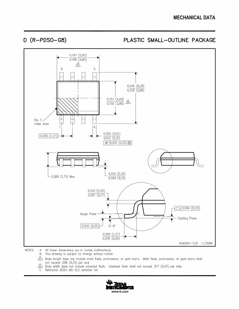
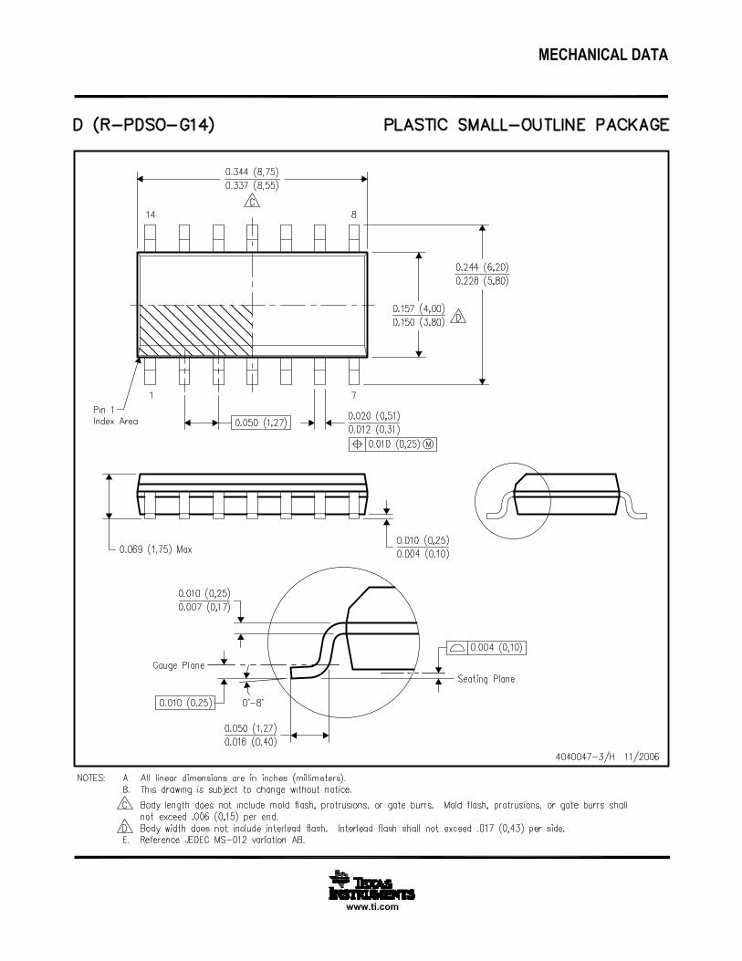
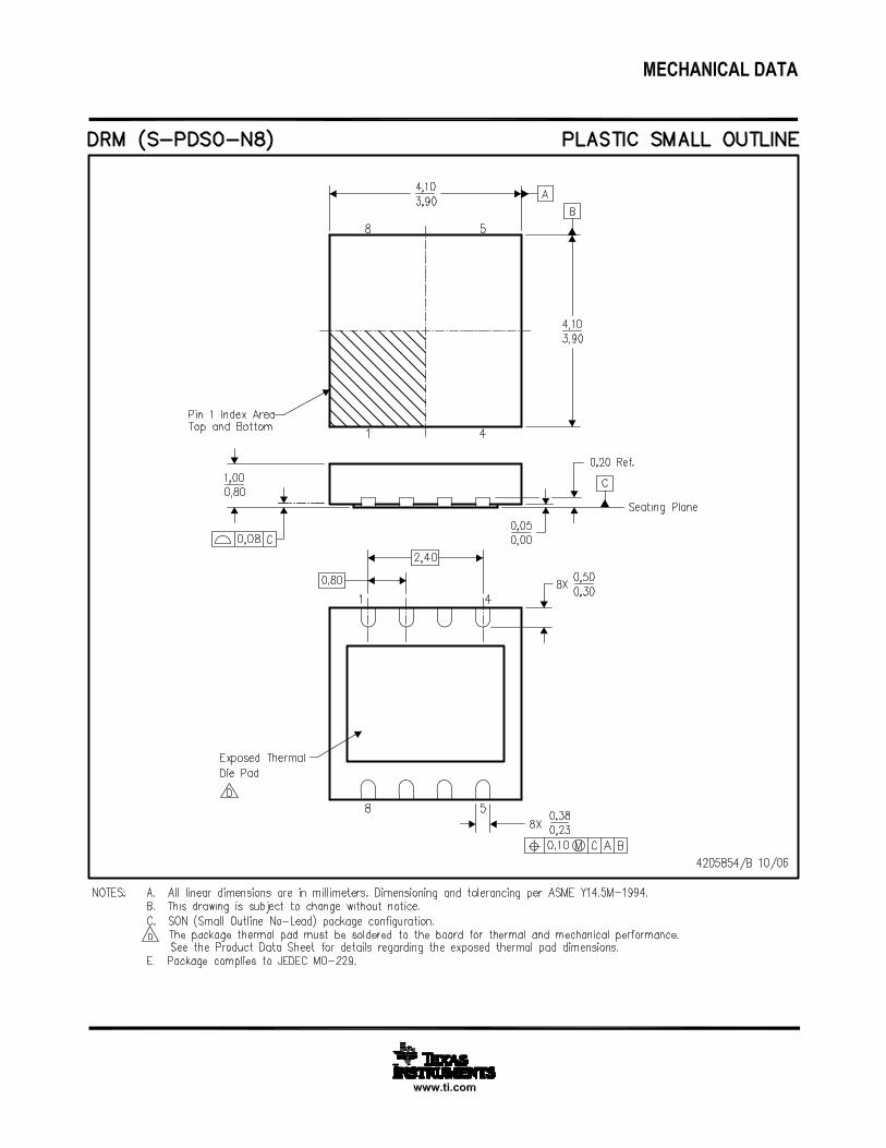
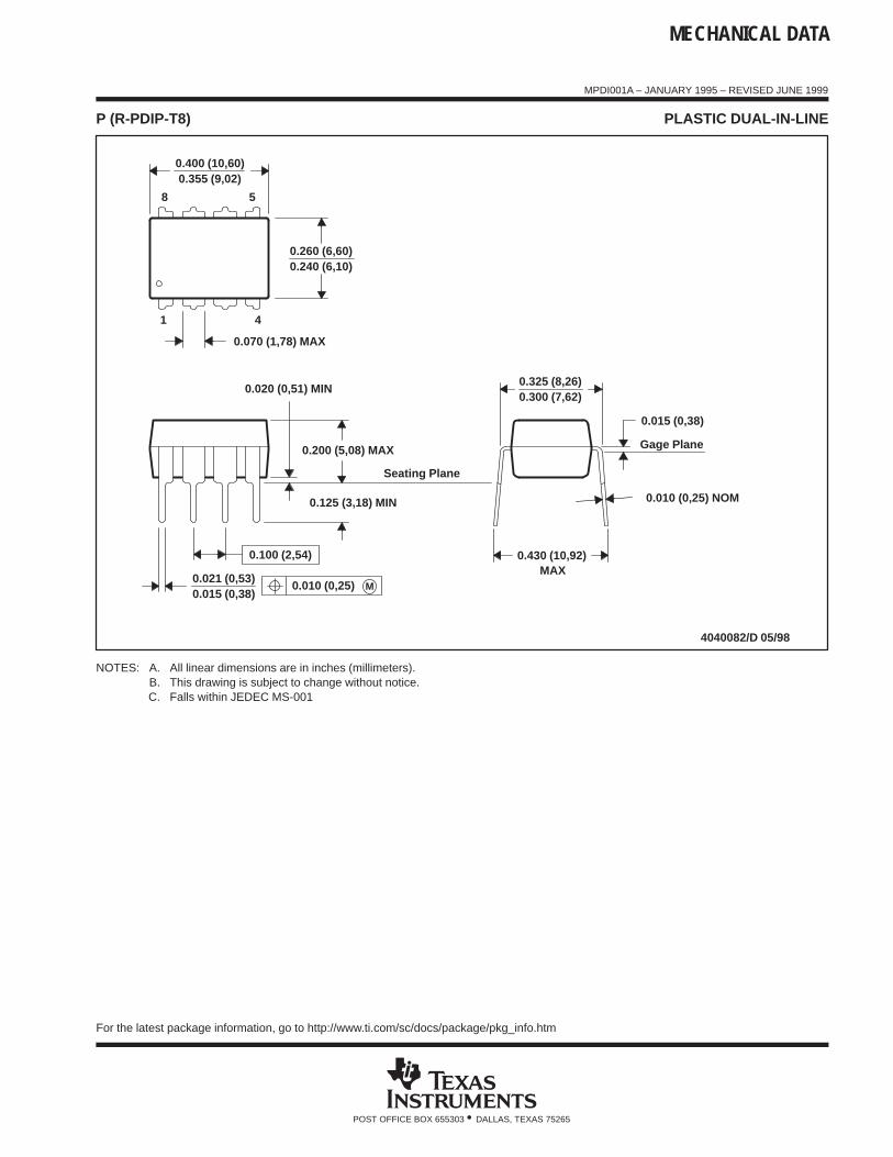
MECHANICAL DATA
MPDI001A – JANUARY 1995 – REVISED JUNE 1999
POST OFFICE BOX 655303 • DALLAS, TEXAS 75265
P (R-PDIP-T8) PLASTIC DUAL-IN-LINE
8
4
0.015 (0,38)
Gage Plane
0.325 (8,26)0.300 (7,62)
0.010 (0,25) NOM
MAX0.430 (10,92)
4040082/D 05/98
0.200 (5,08) MAX
0.125 (3,18) MIN
5
0.355 (9,02)
0.020 (0,51) MIN
0.070 (1,78) MAX
0.240 (6,10)0.260 (6,60)
0.400 (10,60)
1
0.015 (0,38)0.021 (0,53)
Seating Plane
M0.010 (0,25)
0.100 (2,54)
NOTES: A. All linear dimensions are in inches (millimeters).B. This drawing is subject to change without notice.C. Falls within JEDEC MS-001
For the latest package information, go to http://www.ti.com/sc/docs/package/pkg_info.htm
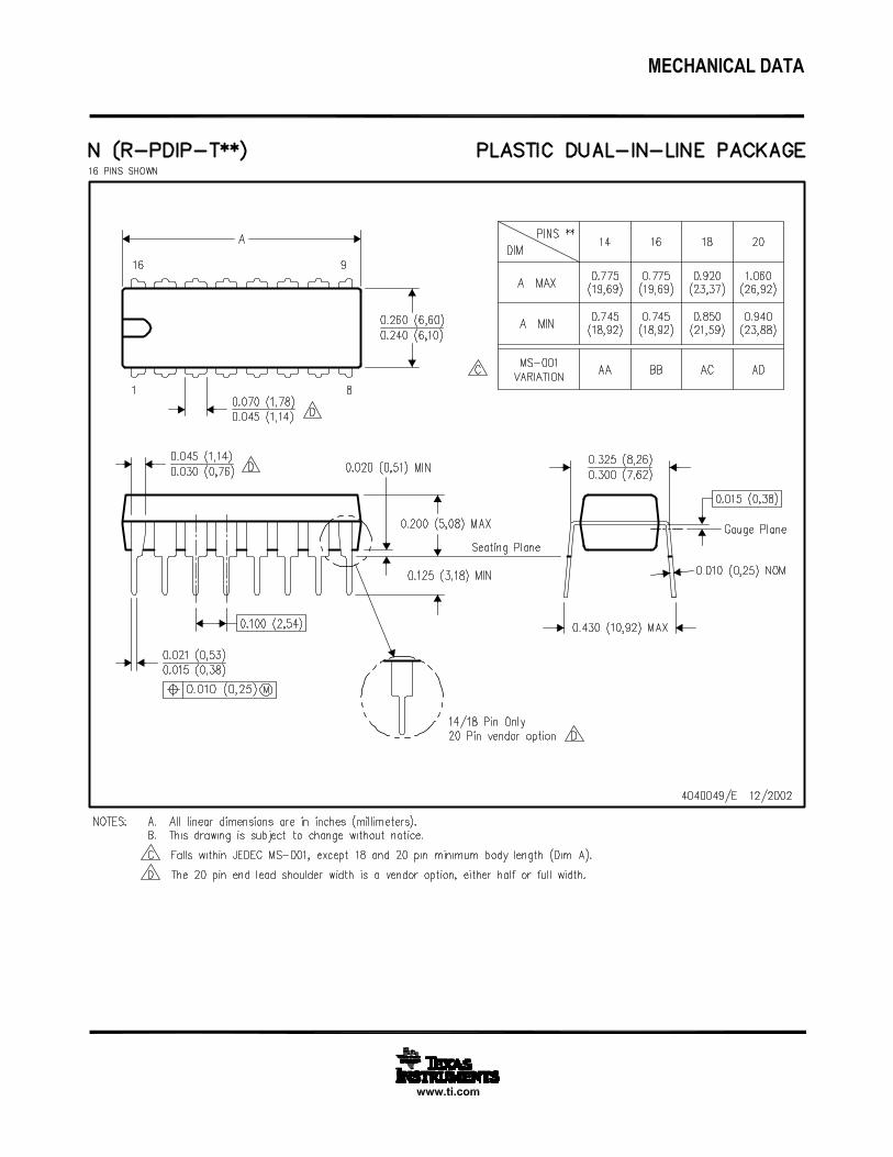

IMPORTANT NOTICETexas Instruments Incorporated and its subsidiaries (TI) reserve the right to make corrections, modifications, enhancements, improvements,and other changes to its products and services at any time and to discontinue any product or service without notice. Customers shouldobtain the latest relevant information before placing orders and should verify that such information is current and complete. All products aresold subject to TI’s terms and conditions of sale supplied at the time of order acknowledgment.TI warrants performance of its hardware products to the specifications applicable at the time of sale in accordance with TI’s standardwarranty. Testing and other quality control techniques are used to the extent TI deems necessary to support this warranty. Except wheremandated by government requirements, testing of all parameters of each product is not necessarily performed.TI assumes no liability for applications assistance or customer product design. Customers are responsible for their products andapplications using TI components. To minimize the risks associated with customer products and applications, customers should provideadequate design and operating safeguards.TI does not warrant or represent that any license, either express or implied, is granted under any TI patent right, copyright, mask work right,or other TI intellectual property right relating to any combination, machine, or process in which TI products or services are used. Informationpublished by TI regarding third-party products or services does not constitute a license from TI to use such products or services or awarranty or endorsement thereof. Use of such information may require a license from a third party under the patents or other intellectualproperty of the third party, or a license from TI under the patents or other intellectual property of TI.Reproduction of TI information in TI data books or data sheets is permissible only if reproduction is without alteration and is accompaniedby all associated warranties, conditions, limitations, and notices. Reproduction of this information with alteration is an unfair and deceptivebusiness practice. TI is not responsible or liable for such altered documentation. Information of third parties may be subject to additionalrestrictions.Resale of TI products or services with statements different from or beyond the parameters stated by TI for that product or service voids allexpress and any implied warranties for the associated TI product or service and is an unfair and deceptive business practice. TI is notresponsible or liable for any such statements.TI products are not authorized for use in safety-critical applications (such as life support) where a failure of the TI product would reasonablybe expected to cause severe personal injury or death, unless officers of the parties have executed an agreement specifically governingsuch use. Buyers represent that they have all necessary expertise in the safety and regulatory ramifications of their applications, andacknowledge and agree that they are solely responsible for all legal, regulatory and safety-related requirements concerning their productsand any use of TI products in such safety-critical applications, notwithstanding any applications-related information or support that may beprovided by TI. Further, Buyers must fully indemnify TI and its representatives against any damages arising out of the use of TI products insuch safety-critical applications.TI products are neither designed nor intended for use in military/aerospace applications or environments unless the TI products arespecifically designated by TI as military-grade or "enhanced plastic." Only products designated by TI as military-grade meet militaryspecifications. Buyers acknowledge and agree that any such use of TI products which TI has not designated as military-grade is solely atthe Buyer's risk, and that they are solely responsible for compliance with all legal and regulatory requirements in connection with such use.TI products are neither designed nor intended for use in automotive applications or environments unless the specific TI products aredesignated by TI as compliant with ISO/TS 16949 requirements. Buyers acknowledge and agree that, if they use any non-designatedproducts in automotive applications, TI will not be responsible for any failure to meet such requirements.Following are URLs where you can obtain information on other Texas Instruments products and application solutions:Products ApplicationsAmplifiers amplifier.ti.com Audio www.ti.com/audioData Converters dataconverter.ti.com Automotive www.ti.com/automotiveDSP dsp.ti.com Broadband www.ti.com/broadbandClocks and Timers www.ti.com/clocks Digital Control www.ti.com/digitalcontrolInterface interface.ti.com Medical www.ti.com/medicalLogic logic.ti.com Military www.ti.com/militaryPower Mgmt power.ti.com Optical Networking www.ti.com/opticalnetworkMicrocontrollers microcontroller.ti.com Security www.ti.com/securityRFID www.ti-rfid.com Telephony www.ti.com/telephonyRF/IF and ZigBee® Solutions www.ti.com/lprf Video & Imaging www.ti.com/video
Wireless www.ti.com/wireless
Mailing Address: Texas Instruments, Post Office Box 655303, Dallas, Texas 75265Copyright © 2008, Texas Instruments Incorporated
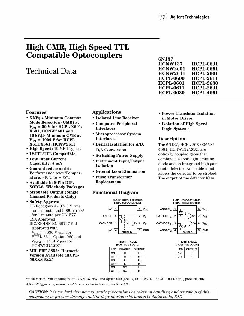
High CMR, High Speed TTLCompatible Optocouplers
Technical Data
6N137HCNW137HCNW2601HCNW2611HCPL-0600HCPL-0601HCPL-0611HCPL-0630
CAUTION: It is advised that normal static precautions be taken in handling and assembly of thiscomponent to prevent damage and/or degradation which may be induced by ESD.
Features• 5 kV/µs Minimum Common
Mode Rejection (CMR) atVCM = 50 V for HCPL-X601/X631, HCNW2601 and10 kV/µs Minimum CMR atVCM = 1000 V for HCPL-X611/X661, HCNW2611
• High Speed: 10 MBd Typical• LSTTL/TTL Compatible• Low Input Current
Capability: 5 mA• Guaranteed ac and dc
Performance over Temper-ature: -40°C to +85°C
• Available in 8-Pin DIP,SOIC-8, Widebody Packages
• Strobable Output (SingleChannel Products Only)
• Safety ApprovalUL Recognized - 3750 V rmsfor 1 minute and 5000 V rms*for 1 minute per UL1577
CSA ApprovedIEC/EN/DIN EN 60747-5-2 Approved with VIORM = 630 V peak forHCPL-2611 Option 060 andVIORM = 1414 V peak forHCNW137/26X1
• MIL-PRF-38534 HermeticVersion Available (HCPL-56XX/66XX)
Functional Diagram
*5000 V rms/1 Minute rating is for HCNW137/26X1 and Option 020 (6N137, HCPL-2601/11/30/31, HCPL-4661) products only.
HCPL-0631HCPL-0661HCPL-2601HCPL-2611HCPL-2630HCPL-2631HCPL-4661
Applications• Isolated Line Receiver• Computer-Peripheral
Interfaces• Microprocessor System
Interfaces• Digital Isolation for A/D,
D/A Conversion• Switching Power Supply• Instrument Input/Output
Isolation• Ground Loop Elimination• Pulse Transformer
Replacement
• Power Transistor Isolationin Motor Drives
• Isolation of High SpeedLogic Systems
DescriptionThe 6N137, HCPL-26XX/06XX/4661, HCNW137/26X1 areoptically coupled gates thatcombine a GaAsP light emittingdiode and an integrated high gainphoto detector. An enable inputallows the detector to be strobed.The output of the detector IC is
A 0.1 µF bypass capacitor must be connected between pins 5 and 8.
1
2
3
4
8
7
6
5
CATHODE
ANODE
GND
V
VCC
O
1
2
3
4
8
7
6
5ANODE 2
CATHODE 2
CATHODE 1
ANODE 1
GND
V
VCC
O2
VE VO1
6N137, HCPL-2601/2611HCPL-0600/0601/0611
HCPL-2630/2631/4661HCPL-0630/0631/0661
NC
NC
LED
ONOFFONOFFONOFF
ENABLE
HHLL
NCNC
OUTPUT
LHHHLH
TRUTH TABLE(POSITIVE LOGIC)
LED
ONOFF
OUTPUT
LH
TRUTH TABLE(POSITIVE LOGIC)
SHIELD SHIELD
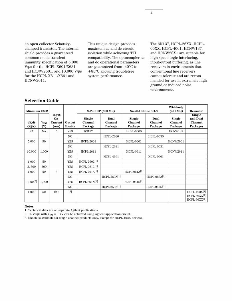
2
an open collector Schottky-clamped transistor. The internalshield provides a guaranteedcommon mode transientimmunity specification of 5,000V/µs for the HCPL-X601/X631and HCNW2601, and 10,000 V/µsfor the HCPL-X611/X661 andHCNW2611.
This unique design providesmaximum ac and dc circuitisolation while achieving TTLcompatibility. The optocoupler acand dc operational parametersare guaranteed from -40°C to+85°C allowing troublefreesystem performance.
The 6N137, HCPL-26XX, HCPL-06XX, HCPL-4661, HCNW137,and HCNW26X1 are suitable forhigh speed logic interfacing,input/output buffering, as linereceivers in environments thatconventional line receiverscannot tolerate and are recom-mended for use in extremely highground or induced noiseenvironments.
Selection GuideWidebody
Minimum CMR 8-Pin DIP (300 Mil) Small-Outline SO-8 (400 Mil) HermeticInput SingleOn- Single Dual Single Dual Single and Dual
dV/dt VCM Current Output Channel Channel Channel Channel Channel Channel(V/µs) (V) (mA) Enable Package Package Package Package Package Packages
NA NA 5 YES 6N137 HCPL-0600 HCNW137
NO HCPL-2630 HCPL-0630
5,000 50 YES HCPL-2601 HCPL-0601 HCNW2601
NO HCPL-2631 HCPL-0631
10,000 1,000 YES HCPL-2611 HCPL-0611 HCNW2611
NO HCPL-4661 HCPL-0661
1,000 50 YES HCPL-2602[1]
3, 500 300 YES HCPL-2612[1]
1,000 50 3 YES HCPL-261A[1] HCPL-061A[1]
NO HCPL-263A[1] HCPL-063A[1]
1,000[2] 1,000 YES HCPL-261N[1] HCPL-061N[1]
NO HCPL-263N[1] HCPL-063N[1]
1,000 50 12.5 [3] HCPL-193X[1]
HCPL-56XX[1]
HCPL-66XX[1]
Notes:1. Technical data are on separate Agilent publications.2. 15 kV/µs with VCM = 1 kV can be achieved using Agilent application circuit.3. Enable is available for single channel products only, except for HCPL-193X devices.
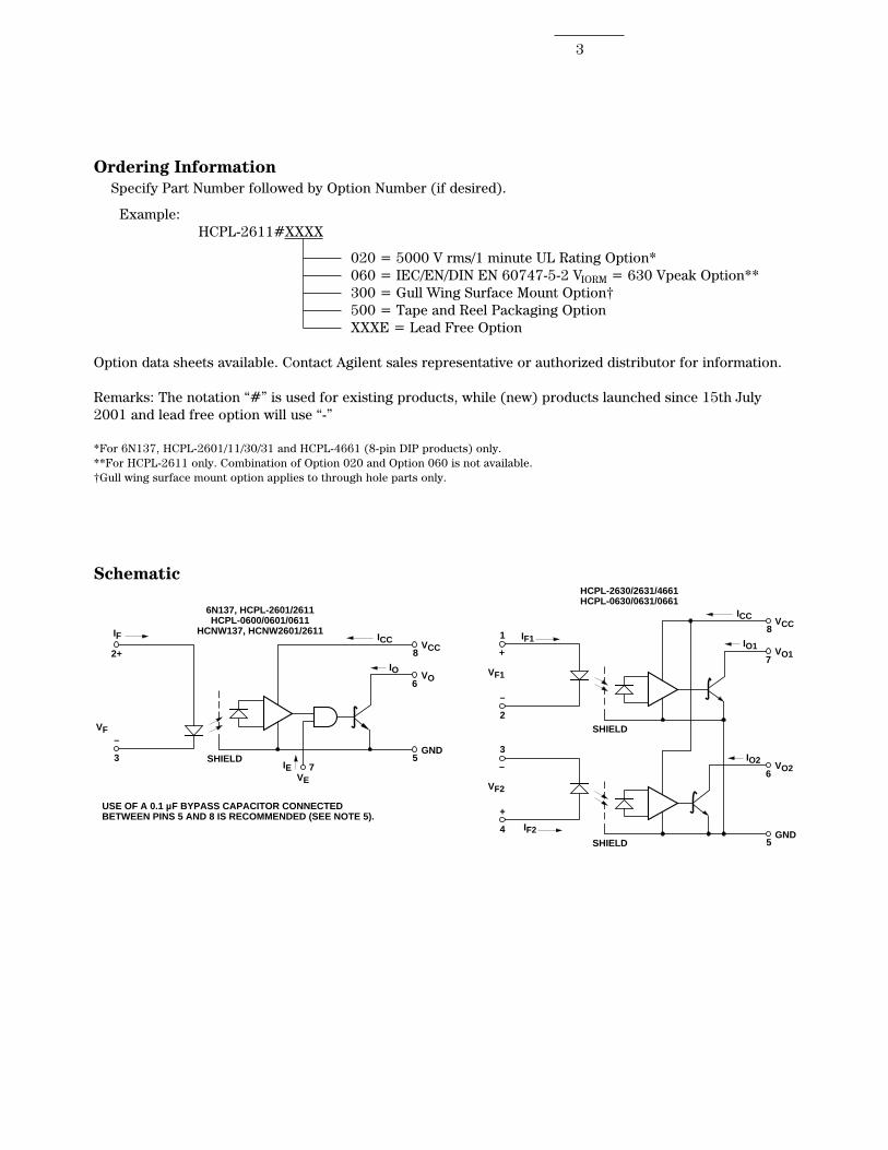
3
Ordering InformationSpecify Part Number followed by Option Number (if desired).
Example:HCPL-2611#XXXX
020 = 5000 V rms/1 minute UL Rating Option*060 = IEC/EN/DIN EN 60747-5-2 VIORM = 630 Vpeak Option**300 = Gull Wing Surface Mount Option†500 = Tape and Reel Packaging OptionXXXE = Lead Free Option
Option data sheets available. Contact Agilent sales representative or authorized distributor for information.
Remarks: The notation “#” is used for existing products, while (new) products launched since 15th July2001 and lead free option will use “-”
*For 6N137, HCPL-2601/11/30/31 and HCPL-4661 (8-pin DIP products) only.**For HCPL-2611 only. Combination of Option 020 and Option 060 is not available.†Gull wing surface mount option applies to through hole parts only.
Schematic
SHIELD
8
6
5
2+
3
VF
USE OF A 0.1 µF BYPASS CAPACITOR CONNECTEDBETWEEN PINS 5 AND 8 IS RECOMMENDED (SEE NOTE 5).
–
IF ICC VCC
VO
GND
IO
VE
IE 7
6N137, HCPL-2601/2611HCPL-0600/0601/0611
HCNW137, HCNW2601/2611
SHIELD
8
7+
2
VF1
–
IF1
ICC VCC
VO1IO1
1
SHIELD
6
5
–
4
VF2
+
IF2
VO2
GND
IO23
HCPL-2630/2631/4661HCPL-0630/0631/0661
4
Package Outline Drawings8-pin DIP Package** (6N137, HCPL-2601/11/30/31, HCPL-4661)
8-pin DIP Package with Gull Wing Surface Mount Option 300(6N137, HCPL-2601/11/30/31, HCPL-4661)
**JEDEC Registered Data (for 6N137 only).
1.080 ± 0.320(0.043 ± 0.013)
2.54 ± 0.25(0.100 ± 0.010)
0.51 (0.020) MIN.
0.65 (0.025) MAX.
4.70 (0.185) MAX.
2.92 (0.115) MIN.
5° TYP. 0.254+ 0.076- 0.051
(0.010+ 0.003)- 0.002)
7.62 ± 0.25(0.300 ± 0.010)
6.35 ± 0.25(0.250 ± 0.010)
9.65 ± 0.25(0.380 ± 0.010)
1.78 (0.070) MAX.1.19 (0.047) MAX.
A XXXXZ
YYWW
DATE CODE
DIMENSIONS IN MILLIMETERS AND (INCHES).
5678
4321
OPTION CODE*
ULRECOGNITION
UR
TYPE NUMBER
*MARKING CODE LETTER FOR OPTION NUMBERS"L" = OPTION 020"V" = OPTION 060OPTION NUMBERS 300 AND 500 NOT MARKED.
NOTE: FLOATING LEAD PROTRUSION IS 0.25 mm (10 mils) MAX.
3.56 ± 0.13(0.140 ± 0.005)
0.635 ± 0.25(0.025 ± 0.010)
12° NOM.
9.65 ± 0.25(0.380 ± 0.010)
0.635 ± 0.130(0.025 ± 0.005)
7.62 ± 0.25(0.300 ± 0.010)
5678
4321
9.65 ± 0.25(0.380 ± 0.010)
6.350 ± 0.25(0.250 ± 0.010)
1.016 (0.040)
1.27 (0.050)
10.9 (0.430)
2.0 (0.080)
LAND PATTERN RECOMMENDATION
1.080 ± 0.320(0.043 ± 0.013)
1.780(0.070)MAX.1.19
(0.047)MAX.
2.54(0.100)BSC
DIMENSIONS IN MILLIMETERS (INCHES).LEAD COPLANARITY = 0.10 mm (0.004 INCHES).
0.254+ 0.076- 0.051
(0.010+ 0.003)- 0.002)
NOTE: FLOATING LEAD PROTRUSION IS 0.25 mm (10 mils) MAX.
3.56 ± 0.13(0.140 ± 0.005)
5
Small-Outline SO-8 Package (HCPL-0600/01/11/30/31/61)
8-Pin Widebody DIP Package (HCNW137, HCNW2601/11)
XXXYWW
8 7 6 5
4321
5.994 ± 0.203(0.236 ± 0.008)
3.937 ± 0.127(0.155 ± 0.005)
0.406 ± 0.076(0.016 ± 0.003) 1.270
(0.050)BSC
5.080 ± 0.127(0.200 ± 0.005)
3.175 ± 0.127(0.125 ± 0.005) 1.524
(0.060)
45° X0.432
(0.017)
0.228 ± 0.025(0.009 ± 0.001)
TYPE NUMBER(LAST 3 DIGITS)
DATE CODE
0.305(0.012)
MIN.TOTAL PACKAGE LENGTH (INCLUSIVE OF MOLD FLASH)5.207 ± 0.254 (0.205 ± 0.010)
DIMENSIONS IN MILLIMETERS (INCHES).LEAD COPLANARITY = 0.10 mm (0.004 INCHES) MAX.
NOTE: FLOATING LEAD PROTRUSION IS 0.15 mm (6 mils) MAX.
0.203 ± 0.102(0.008 ± 0.004)
7°
PIN ONE
0 ~ 7°
*
*
7.49 (0.295)
1.9 (0.075)
0.64 (0.025)
LAND PATTERN RECOMMENDATION
5678
4321
11.15 ± 0.15(0.442 ± 0.006)
1.78 ± 0.15(0.070 ± 0.006)
5.10(0.201)
MAX.
1.55(0.061)MAX.
2.54 (0.100)TYP.
DIMENSIONS IN MILLIMETERS (INCHES).
NOTE: FLOATING LEAD PROTRUSION IS 0.25 mm (10 mils) MAX.
7° TYP.0.254
+ 0.076- 0.0051
(0.010+ 0.003)- 0.002)
11.00(0.433)
9.00 ± 0.15(0.354 ± 0.006)
MAX.
10.16 (0.400)TYP.
A HCNWXXXX
YYWW
DATE CODE
TYPE NUMBER
0.51 (0.021) MIN.
0.40 (0.016)0.56 (0.022)
3.10 (0.122)3.90 (0.154)
6
8-Pin Widebody DIP Package with Gull Wing Surface Mount Option 300(HCNW137, HCNW2601/11)
Solder Reflow Temperature Profile
0
TIME (SECONDS)
TE
MP
ER
AT
UR
E (
°C)
200
100
50 150100 200 250
300
0
30SEC.
50 SEC.
30SEC.
160°C
140°C150°C
PEAKTEMP.245°C
PEAKTEMP.240°C
PEAKTEMP.230°C
SOLDERINGTIME200°C
PREHEATING TIME150°C, 90 + 30 SEC.
2.5°C ± 0.5°C/SEC.
3°C + 1°C/–0.5°C
TIGHTTYPICALLOOSE
ROOMTEMPERATURE
PREHEATING RATE 3°C + 1°C/–0.5°C/SEC.REFLOW HEATING RATE 2.5°C ± 0.5°C/SEC.
1.00 ± 0.15(0.039 ± 0.006)
7° NOM.
12.30 ± 0.30(0.484 ± 0.012)
0.75 ± 0.25(0.030 ± 0.010)
11.00(0.433)
5678
4321
11.15 ± 0.15(0.442 ± 0.006)
9.00 ± 0.15(0.354 ± 0.006)
1.3(0.051)
13.56(0.534)
2.29(0.09)
LAND PATTERN RECOMMENDATION
1.78 ± 0.15(0.070 ± 0.006)
4.00(0.158)
MAX.
1.55(0.061)MAX.
2.54(0.100)BSC
DIMENSIONS IN MILLIMETERS (INCHES).
LEAD COPLANARITY = 0.10 mm (0.004 INCHES).
NOTE: FLOATING LEAD PROTRUSION IS 0.25 mm (10 mils) MAX.
0.254+ 0.076- 0.0051
(0.010+ 0.003)- 0.002)
MAX.
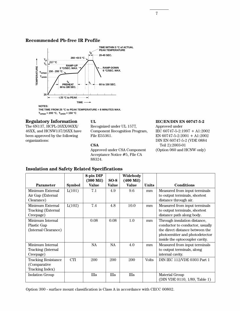
7
Regulatory InformationThe 6N137, HCPL-26XX/06XX/46XX, and HCNW137/26XX havebeen approved by the followingorganizations:
ULRecognized under UL 1577,Component Recognition Program,File E55361.
CSAApproved under CSA ComponentAcceptance Notice #5, File CA88324.
Insulation and Safety Related Specifications8-pin DIP Widebody (300 Mil) SO-8 (400 Mil)
Parameter Symbol Value Value Value Units ConditionsMinimum External L(101) 7.1 4.9 9.6 mm Measured from input terminalsAir Gap (External to output terminals, shortestClearance) distance through air.Minimum External L(102) 7.4 4.8 10.0 mm Measured from input terminalsTracking (External to output terminals, shortestCreepage) distance path along body.Minimum Internal 0.08 0.08 1.0 mm Through insulation distance,Plastic Gap conductor to conductor, usually(Internal Clearance) the direct distance between the
photoemitter and photodetectorinside the optocoupler cavity.
Minimum Internal NA NA 4.0 mm Measured from input terminalsTracking (Internal to output terminals, alongCreepage) internal cavity.Tracking Resistance CTI 200 200 200 Volts DIN IEC 112/VDE 0303 Part 1(ComparativeTracking Index)Isolation Group IIIa IIIa IIIa Material Group
(DIN VDE 0110, 1/89, Table 1)
Option 300 - surface mount classification is Class A in accordance with CECC 00802.
Recommended Pb-free IR Profile
IEC/EN/DIN EN 60747-5-2Approved underIEC 60747-5-2:1997 + A1:2002EN 60747-5-2:2001 + A1:2002DIN EN 60747-5-2 (VDE 0884 Teil 2):2003-01(Option 060 and HCNW only)
217 °C
RAMP-DOWN6 °C/SEC. MAX.
RAMP-UP3 °C/SEC. MAX.
150 - 200 °C
260 +0/-5 °C
t 25 °C to PEAK
60 to 150 SEC.
20-40 SEC.
TIME WITHIN 5 °C of ACTUALPEAK TEMPERATURE
tp
tsPREHEAT
60 to 180 SEC.
tL
TL
TsmaxTsmin
25
Tp
TIME
TE
MP
ER
AT
UR
E
NOTES:THE TIME FROM 25 °C to PEAK TEMPERATURE = 8 MINUTES MAX.Tsmax = 200 °C, Tsmin = 150 °C
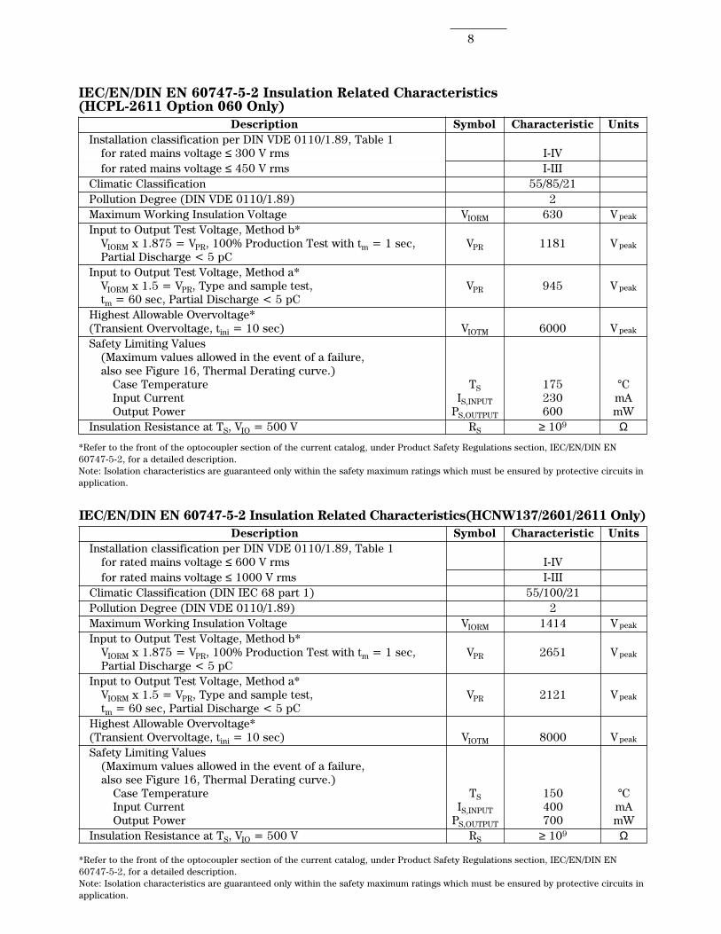
8
IEC/EN/DIN EN 60747-5-2 Insulation Related Characteristics(HCPL-2611 Option 060 Only)
Description Symbol Characteristic UnitsInstallation classification per DIN VDE 0110/1.89, Table 1
for rated mains voltage ≤ 300 V rms I-IVfor rated mains voltage ≤ 450 V rms I-III
Climatic Classification 55/85/21Pollution Degree (DIN VDE 0110/1.89) 2Maximum Working Insulation Voltage VIORM 630 V peak
Input to Output Test Voltage, Method b*VIORM x 1.875 = VPR, 100% Production Test with tm = 1 sec, VPR 1181 V peak
Partial Discharge < 5 pCInput to Output Test Voltage, Method a*
VIORM x 1.5 = VPR, Type and sample test, VPR 945 V peak
tm = 60 sec, Partial Discharge < 5 pCHighest Allowable Overvoltage*(Transient Overvoltage, tini = 10 sec) VIOTM 6000 V peak
Safety Limiting Values(Maximum values allowed in the event of a failure,also see Figure 16, Thermal Derating curve.)
Case Temperature TS 175 °CInput Current IS,INPUT 230 mAOutput Power PS,OUTPUT 600 mW
Insulation Resistance at TS, VIO = 500 V RS ≥ 109 Ω
*Refer to the front of the optocoupler section of the current catalog, under Product Safety Regulations section, IEC/EN/DIN EN60747-5-2, for a detailed description.Note: Isolation characteristics are guaranteed only within the safety maximum ratings which must be ensured by protective circuits inapplication.
IEC/EN/DIN EN 60747-5-2 Insulation Related Characteristics(HCNW137/2601/2611 Only)Description Symbol Characteristic Units
Installation classification per DIN VDE 0110/1.89, Table 1for rated mains voltage ≤ 600 V rms I-IVfor rated mains voltage ≤ 1000 V rms I-III
Climatic Classification (DIN IEC 68 part 1) 55/100/21Pollution Degree (DIN VDE 0110/1.89) 2Maximum Working Insulation Voltage VIORM 1414 V peak
Input to Output Test Voltage, Method b*VIORM x 1.875 = VPR, 100% Production Test with tm = 1 sec, VPR 2651 V peak
Partial Discharge < 5 pCInput to Output Test Voltage, Method a*
VIORM x 1.5 = VPR, Type and sample test, VPR 2121 V peak
tm = 60 sec, Partial Discharge < 5 pCHighest Allowable Overvoltage*(Transient Overvoltage, tini = 10 sec) VIOTM 8000 V peak
Safety Limiting Values(Maximum values allowed in the event of a failure,also see Figure 16, Thermal Derating curve.)
Case Temperature TS 150 °CInput Current IS,INPUT 400 mAOutput Power PS,OUTPUT 700 mW
Insulation Resistance at TS, VIO = 500 V RS ≥ 109 Ω
*Refer to the front of the optocoupler section of the current catalog, under Product Safety Regulations section, IEC/EN/DIN EN60747-5-2, for a detailed description.Note: Isolation characteristics are guaranteed only within the safety maximum ratings which must be ensured by protective circuits inapplication.

9
Absolute Maximum Ratings* (No Derating Required up to 85°C)Parameter Symbol Package** Min. Max. Units Note
Storage Temperature TS -55 125 °COperating Temperature† TA -40 85 °CAverage Forward Input Current IF Single 8-Pin DIP 20 mA 2
Single SO-8Widebody
Dual 8-Pin DIP 15 1, 3Dual SO-8
Reverse Input Voltage VR 8-Pin DIP, SO-8 5 V 1Widebody 3
Input Power Dissipation PI Widebody 40 mWSupply Voltage VCC 7 V(1 Minute Maximum)Enable Input Voltage (Not to VE Single 8-Pin DIP VCC + 0.5 VExceed VCC by more than Single SO-8500 mV) WidebodyEnable Input Current IE 5 mAOutput Collector Current IO 50 mA 1Output Collector Voltage VO 7 V 1Output Collector Power PO Single 8-Pin DIP 85 mWDissipation Single SO-8
WidebodyDual 8-Pin DIP 60 1, 4
Dual SO-8Lead Solder Temperature TLS 8-Pin DIP 260°C for 10 sec.,(Through Hole Parts Only) 1.6 mm below seating plane
Widebody 260°C for 10 sec.,up to seating plane
Solder Reflow Temperature SO-8 and See Package OutlineProfile (Surface Mount Parts Only) Option 300 Drawings section
*JEDEC Registered Data (for 6N137 only).**Ratings apply to all devices except otherwise noted in the Package column.†0°C to 70°C on JEDEC Registration.
Recommended Operating ConditionsParameter Symbol Min. Max. Units
Input Current, Low Level IFL* 0 250 µAInput Current, High Level[1] IFH** 5 15 mAPower Supply Voltage VCC 4.5 5.5 VLow Level Enable Voltage† VEL 0 0.8 VHigh Level Enable Voltage† VEH 2.0 VCC VOperating Temperature TA -40 85 °CFan Out (at RL = 1 kΩ)[1] N 5 TTL LoadsOutput Pull-up Resistor RL 330 4 k Ω
*The off condition can also be guaranteed by ensuring that VFL ≤ 0.8 volts.**The initial switching threshold is 5 mA or less. It is recommended that 6.3 mA to 10 mA be used for best performance and to permitat least a 20% LED degradation guardband.†For single channel products only.
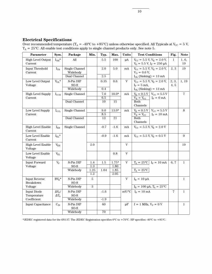
10
Electrical SpecificationsOver recommended temperature (TA = -40°C to +85°C) unless otherwise specified. All Typicals at VCC = 5 V,TA = 25°C. All enable test conditions apply to single channel products only. See note 5.
Parameter Sym. Package Min. Typ. Max. Units Test Conditions Fig. Note
High Level Output IOH* All 5.5 100 µA VCC = 5.5 V, VE = 2.0 V, 1 1, 6,Current VO = 5.5 V, IF = 250 µA 19
Input Threshold ITH Single Channel 2.0 5.0 mA VCC = 5.5 V, VE = 2.0 V, 2, 3 19Current Widebody VO = 0.6 V,
Dual Channel 2.5 IOL (Sinking) = 13 mA
Low Level Output VOL* 8-Pin DIP 0.35 0.6 V VCC = 5.5 V, VE = 2.0 V, 2, 3, 1, 19Voltage SO-8 IF = 5 mA, 4, 5
Widebody 0.4 IOL (Sinking) = 13 mA
High Level Supply ICCH Single Channel 7.0 10.0* mA VE = 0.5 V VCC = 5.5 V 7Current 6.5 VE = VCC IF = 0 mA
Dual Channel 10 15 BothChannels
Low Level Supply ICCL Single Channel 9.0 13.0* mA VE = 0.5 V VCC = 5.5 V 8Current 8.5 VE = VCC IF = 10 mA
Dual Channel 13 21 BothChannels
High Level Enable IEH Single Channel -0.7 -1.6 mA VCC = 5.5 V, VE = 2.0 VCurrent
Low Level Enable IEL* -0.9 -1.6 mA VCC = 5.5 V, VE = 0.5 V 9Current
High Level Enable VEH 2.0 V 19Voltage
Low Level Enable VEL 0.8 VVoltage
Input Forward VF 8-Pin DIP 1.4 1.5 1.75* V TA = 25°C IF = 10 mA 6, 7 1Voltage SO-8 1.3 1.80
Widebody 1.25 1.64 1.85 TA = 25°C1.2 2.05
Input Reverse BVR* 8-Pin DIP 5 V IR = 10 µA 1Breakdown SO-8Voltage Widebody 3 IR = 100 µA, TA = 25°CInput Diode ∆VF/ 8-Pin DIP -1.6 mV/°C IF = 10 mA 7 1Temperature ∆TA SO-8Coefficient Widebody -1.9
Input Capacitance CIN 8-Pin DIP 60 pF f = 1 MHz, VF = 0 V 1SO-8
Widebody 70
*JEDEC registered data for the 6N137. The JEDEC Registration specifies 0°C to +70°C. HP specifies -40°C to +85°C.
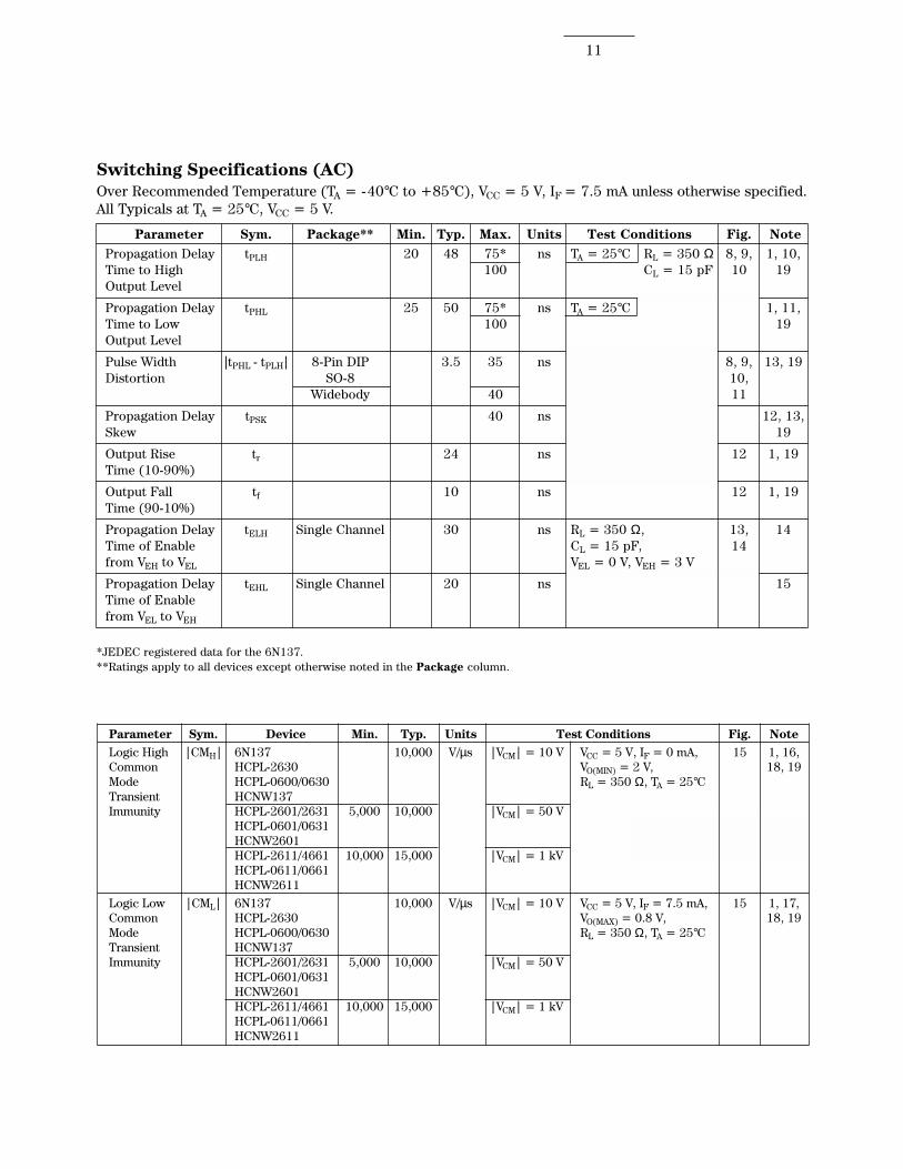
11
Switching Specifications (AC)Over Recommended Temperature (TA = -40°C to +85°C), VCC = 5 V, IF
= 7.5 mA unless otherwise specified.All Typicals at TA = 25°C, VCC = 5 V.
Parameter Sym. Package** Min. Typ. Max. Units Test Conditions Fig. NotePropagation Delay tPLH 20 48 75* ns TA = 25°C RL = 350 Ω 8, 9, 1, 10,Time to High 100 CL = 15 pF 10 19Output Level
Propagation Delay tPHL 25 50 75* ns TA = 25°C 1, 11,Time to Low 100 19Output Level
Pulse Width |tPHL - tPLH| 8-Pin DIP 3.5 35 ns 8, 9, 13, 19Distortion SO-8 10,
Widebody 40 11
Propagation Delay tPSK 40 ns 12, 13,Skew 19
Output Rise tr 24 ns 12 1, 19Time (10-90%)
Output Fall tf 10 ns 12 1, 19Time (90-10%)
Propagation Delay tELH Single Channel 30 ns RL = 350 Ω, 13, 14Time of Enable CL = 15 pF, 14from VEH to VEL VEL = 0 V, VEH = 3 V
Propagation Delay tEHL Single Channel 20 ns 15Time of Enablefrom VEL to VEH
*JEDEC registered data for the 6N137.**Ratings apply to all devices except otherwise noted in the Package column.
Parameter Sym. Device Min. Typ. Units Test Conditions Fig. NoteLogic High |CMH| 6N137 10,000 V/µs |VCM| = 10 V VCC = 5 V, IF = 0 mA, 15 1, 16,Common HCPL-2630 VO(MIN) = 2 V, 18, 19Mode HCPL-0600/0630 RL = 350 Ω, TA = 25°CTransient HCNW137Immunity HCPL-2601/2631 5,000 10,000 |VCM| = 50 V
HCPL-0601/0631HCNW2601HCPL-2611/4661 10,000 15,000 |VCM| = 1 kVHCPL-0611/0661HCNW2611
Logic Low |CML| 6N137 10,000 V/µs |VCM| = 10 V VCC = 5 V, IF = 7.5 mA, 15 1, 17,Common HCPL-2630 VO(MAX) = 0.8 V, 18, 19Mode HCPL-0600/0630 RL = 350 Ω, TA = 25°CTransient HCNW137Immunity HCPL-2601/2631 5,000 10,000 |VCM| = 50 V
HCPL-0601/0631HCNW2601HCPL-2611/4661 10,000 15,000 |VCM| = 1 kVHCPL-0611/0661HCNW2611
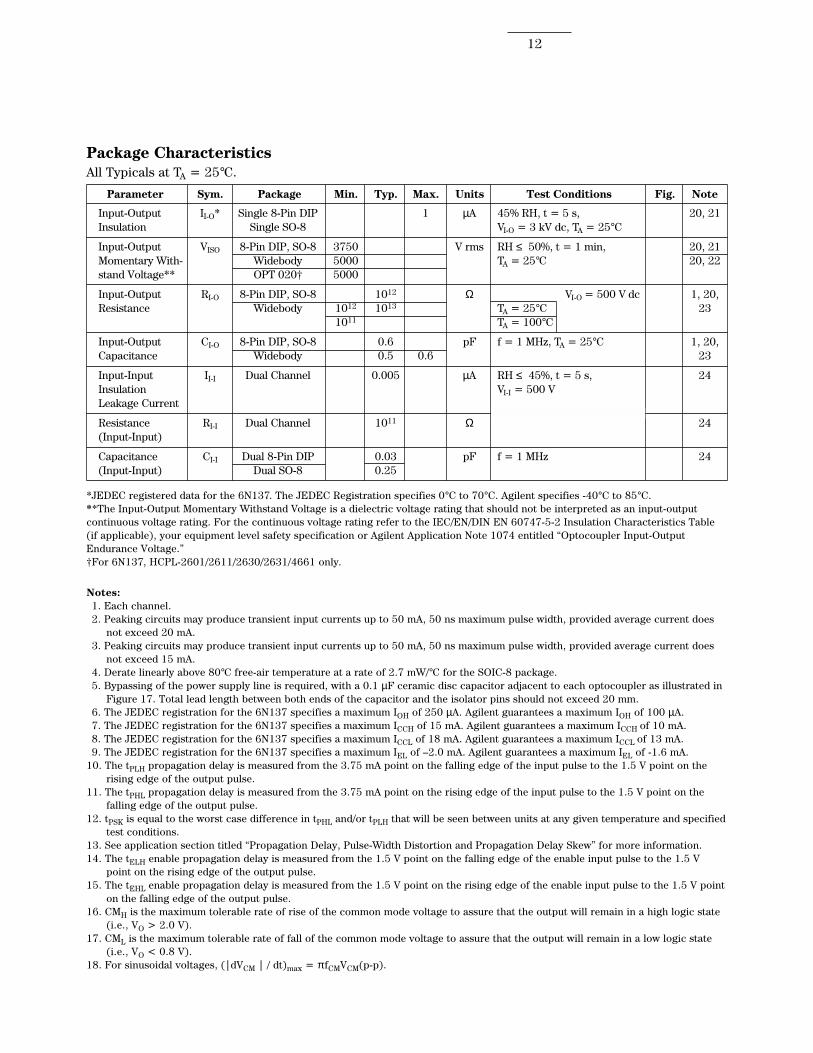
12
Package CharacteristicsAll Typicals at TA = 25°C.
Parameter Sym. Package Min. Typ. Max. Units Test Conditions Fig. Note
Input-Output II-O* Single 8-Pin DIP 1 µA 45% RH, t = 5 s, 20, 21Insulation Single SO-8 VI-O = 3 kV dc, TA = 25°C
Input-Output VISO 8-Pin DIP, SO-8 3750 V rms RH ≤ 50%, t = 1 min, 20, 21Momentary With- Widebody 5000 TA = 25°C 20, 22stand Voltage** OPT 020† 5000
Input-Output RI-O 8-Pin DIP, SO-8 1012 Ω VI-O = 500 V dc 1, 20,Resistance Widebody 1012 1013 TA = 25°C 23
1011 TA = 100°C
Input-Output CI-O 8-Pin DIP, SO-8 0.6 pF f = 1 MHz, TA = 25°C 1, 20,Capacitance Widebody 0.5 0.6 23
Input-Input II-I Dual Channel 0.005 µA RH ≤ 45%, t = 5 s, 24Insulation VI-I = 500 VLeakage Current
Resistance RI-I Dual Channel 1011 Ω 24(Input-Input)
Capacitance CI-I Dual 8-Pin DIP 0.03 pF f = 1 MHz 24(Input-Input) Dual SO-8 0.25
*JEDEC registered data for the 6N137. The JEDEC Registration specifies 0°C to 70°C. Agilent specifies -40°C to 85°C.**The Input-Output Momentary Withstand Voltage is a dielectric voltage rating that should not be interpreted as an input-outputcontinuous voltage rating. For the continuous voltage rating refer to the IEC/EN/DIN EN 60747-5-2 Insulation Characteristics Table(if applicable), your equipment level safety specification or Agilent Application Note 1074 entitled “Optocoupler Input-OutputEndurance Voltage.”†For 6N137, HCPL-2601/2611/2630/2631/4661 only.
Notes:1. Each channel.2. Peaking circuits may produce transient input currents up to 50 mA, 50 ns maximum pulse width, provided average current does
not exceed 20 mA.3. Peaking circuits may produce transient input currents up to 50 mA, 50 ns maximum pulse width, provided average current does
not exceed 15 mA.4. Derate linearly above 80°C free-air temperature at a rate of 2.7 mW/°C for the SOIC-8 package.5. Bypassing of the power supply line is required, with a 0.1 µF ceramic disc capacitor adjacent to each optocoupler as illustrated in
Figure 17. Total lead length between both ends of the capacitor and the isolator pins should not exceed 20 mm.6. The JEDEC registration for the 6N137 specifies a maximum IOH of 250 µA. Agilent guarantees a maximum IOH of 100 µA.7. The JEDEC registration for the 6N137 specifies a maximum ICCH of 15 mA. Agilent guarantees a maximum ICCH of 10 mA.8. The JEDEC registration for the 6N137 specifies a maximum ICCL of 18 mA. Agilent guarantees a maximum ICCL of 13 mA.9. The JEDEC registration for the 6N137 specifies a maximum IEL of –2.0 mA. Agilent guarantees a maximum IEL of -1.6 mA.
10. The tPLH propagation delay is measured from the 3.75 mA point on the falling edge of the input pulse to the 1.5 V point on therising edge of the output pulse.
11. The tPHL propagation delay is measured from the 3.75 mA point on the rising edge of the input pulse to the 1.5 V point on thefalling edge of the output pulse.
12. tPSK is equal to the worst case difference in tPHL and/or tPLH that will be seen between units at any given temperature and specifiedtest conditions.
13. See application section titled “Propagation Delay, Pulse-Width Distortion and Propagation Delay Skew” for more information.14. The tELH enable propagation delay is measured from the 1.5 V point on the falling edge of the enable input pulse to the 1.5 V
point on the rising edge of the output pulse.15. The tEHL enable propagation delay is measured from the 1.5 V point on the rising edge of the enable input pulse to the 1.5 V point
on the falling edge of the output pulse.16. CMH is the maximum tolerable rate of rise of the common mode voltage to assure that the output will remain in a high logic state
(i.e., VO > 2.0 V).17. CML is the maximum tolerable rate of fall of the common mode voltage to assure that the output will remain in a low logic state
(i.e., VO < 0.8 V).18. For sinusoidal voltages, (|dVCM | / dt)max = πfCMVCM(p-p).
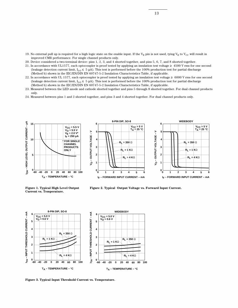
13
I OH
– H
IGH
LE
VE
L O
UT
PU
T C
UR
RE
NT
– µ
A
-600
TA – TEMPERATURE – °C
100
10
15
-20
5
20
VCC = 5.5 VVO = 5.5 VVE = 2.0 V*IF = 250 µA
60-40 0 40 80
* FOR SINGLE CHANNEL PRODUCTS ONLY
19. No external pull up is required for a high logic state on the enable input. If the VE pin is not used, tying VE to VCC will result inimproved CMR performance. For single channel products only.
20. Device considered a two-terminal device: pins 1, 2, 3, and 4 shorted together, and pins 5, 6, 7, and 8 shorted together.21. In accordance with UL1577, each optocoupler is proof tested by applying an insulation test voltage ≥ 4500 V rms for one second
(leakage detection current limit, II-O ≤ 5 µA). This test is performed before the 100% production test for partial discharge(Method b) shown in the IEC/EN/DIN EN 60747-5-2 Insulation Characteristics Table, if applicable.
22. In accordance with UL 1577, each optocoupler is proof tested by applying an insulation test voltage ≥ 6000 V rms for one second(leakage detection current limit, II-O ≤ 5 µA). This test is performed before the 100% production test for partial discharge(Method b) shown in the IEC/EN/DIN EN 60747-5-2 Insulation Characteristics Table, if applicable.
23. Measured between the LED anode and cathode shorted together and pins 5 through 8 shorted together. For dual channel productsonly.
24. Measured between pins 1 and 2 shorted together, and pins 3 and 4 shorted together. For dual channel products only.
Figure 2. Typical Output Voltage vs. Forward Input Current.
Figure 3. Typical Input Threshold Current vs. Temperature.
Figure 1. Typical High Level OutputCurrent vs. Temperature.
1
6
2
3
4
5
1 2 3 4 5 6
IF – FORWARD INPUT CURRENT – mA
RL = 350 Ω
RL = 1 KΩ
RL = 4 KΩ
00
VCC = 5 VTA = 25 °C
VO
– O
UT
PU
T V
OL
TA
GE
– V
8-PIN DIP, SO-8
1
6
2
3
4
5
1 2 3 4 5 6
IF – FORWARD INPUT CURRENT – mA
RL = 350 Ω
RL = 1 KΩ
RL = 4 KΩ
00
VCC = 5 VTA = 25 °C
VO
– O
UT
PU
T V
OL
TA
GE
– V
WIDEBODY
VCC = 5.0 VVO = 0.6 V
6
3
-60 -20 20 60 100
TA – TEMPERATURE – °C
2
80400-400
I TH
– IN
PU
T T
HR
ES
HO
LD
CU
RR
EN
T –
mA
RL = 350 Ω
1
4
5
RL = 1 KΩ
RL = 4 KΩ
WIDEBODY
VCC = 5.0 VVO = 0.6 V
6
3
-60 -20 20 60 100
TA – TEMPERATURE – °C
2
80400-400
I TH
– IN
PU
T T
HR
ES
HO
LD
CU
RR
EN
T –
mA
RL = 350 Ω
1
4
5
RL = 1 KΩ
RL = 4 KΩ
8-PIN DIP, SO-8
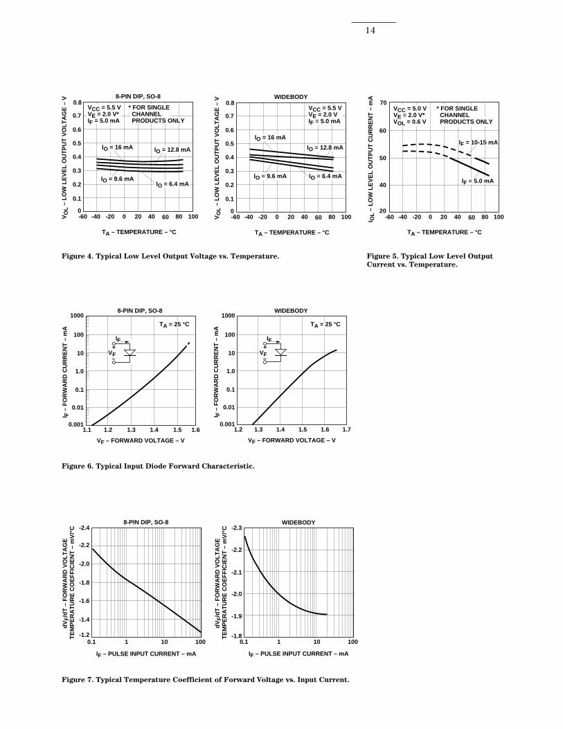
14
I F –
FO
RW
AR
D C
UR
RE
NT
– m
A
1.20.001
VF – FORWARD VOLTAGE – V
1.0
1000
1.4
0.01
1.61.3 1.5
0.1
10
100
WIDEBODY
IF+
–VF
1.7
TA = 25 °C
VCC = 5.0 VVE = 2.0 V*VOL = 0.6 V
70
60
-60 -20 20 60 100
TA – TEMPERATURE – °C
50
80400-4020
I OL
– L
OW
LE
VE
L O
UT
PU
T C
UR
RE
NT
– m
A
40
IF = 10-15 mA
IF = 5.0 mA
* FOR SINGLE CHANNEL PRODUCTS ONLY
0.8
0.4
-60 -20 20 60 100
TA – TEMPERATURE – °C
0.2
80400-400
VO
L –
LO
W L
EV
EL
OU
TP
UT
VO
LT
AG
E –
V
IO = 16 mA
0.1
0.5
0.7
IO = 6.4 mA
WIDEBODY
VCC = 5.5 VVE = 2.0 VIF = 5.0 mA
0.3
0.6
IO = 12.8 mA
IO = 9.6 mA
Figure 7. Typical Temperature Coefficient of Forward Voltage vs. Input Current.
Figure 4. Typical Low Level Output Voltage vs. Temperature. Figure 5. Typical Low Level OutputCurrent vs. Temperature.
Figure 6. Typical Input Diode Forward Characteristic.
0.8
0.4
-60 -20 20 60 100
TA – TEMPERATURE – °C
0.2
80400-400
VO
L –
LO
W L
EV
EL
OU
TP
UT
VO
LT
AG
E –
V
IO = 16 mA
0.1
0.5
0.7
IO = 6.4 mA
8-PIN DIP, SO-8
VCC = 5.5 VVE = 2.0 V*IF = 5.0 mA
0.3
0.6
IO = 12.8 mA
IO = 9.6 mA
* FOR SINGLE CHANNEL PRODUCTS ONLY
I F –
FO
RW
AR
D C
UR
RE
NT
– m
A
1.10.001
VF – FORWARD VOLTAGE – V
1.0
1000
1.3
0.01
1.51.2 1.4
0.1
TA = 25 °C
10
100
8-PIN DIP, SO-8
IF+
–VF
1.6
dV
F/d
T –
FO
RW
AR
D V
OL
TA
GE
T
EM
PE
RA
TU
RE
CO
EF
FIC
IEN
T –
mV
/°C
0.1 1 10 100
IF – PULSE INPUT CURRENT – mA
-1.4
-2.2
-2.0
-1.8
-1.6
-1.2
-2.48-PIN DIP, SO-8
dV
F/d
T –
FO
RW
AR
D V
OL
TA
GE
T
EM
PE
RA
TU
RE
CO
EF
FIC
IEN
T –
mV
/°C
0.1 1 10 100
IF – PULSE INPUT CURRENT – mA
-1.9
-2.2
-2.1
-2.0
-1.8
-2.3WIDEBODY
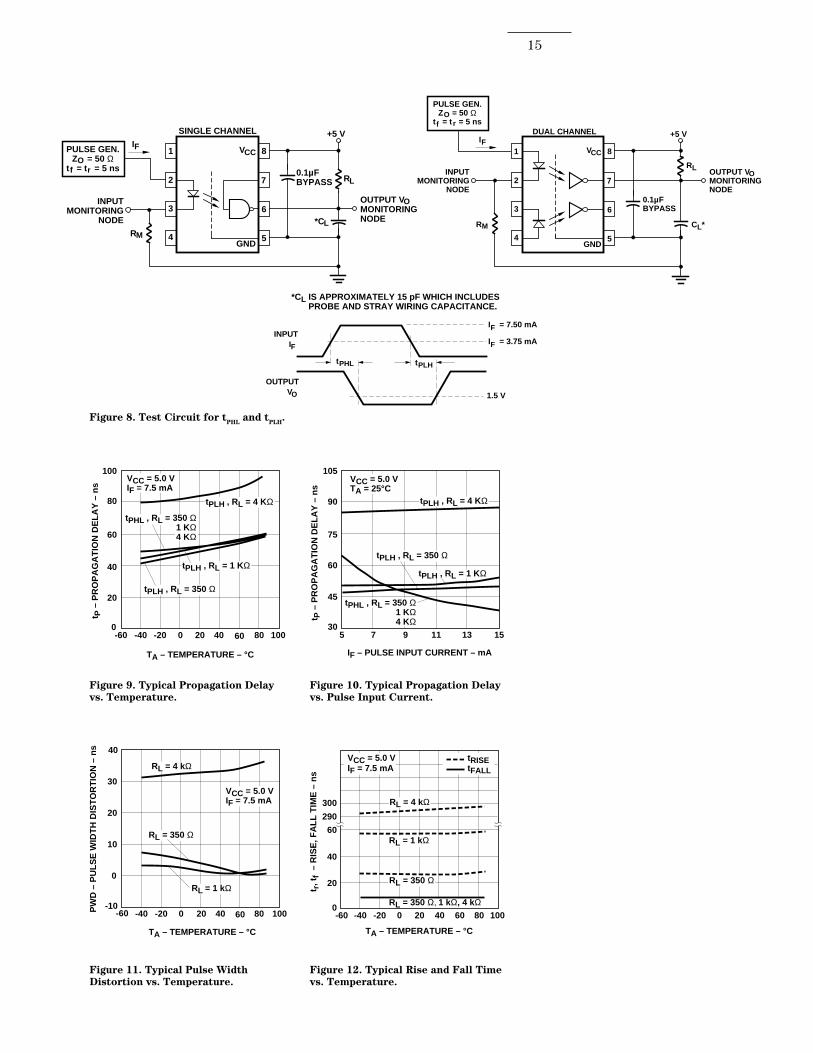
15
VCC = 5.0 VIF = 7.5 mA
40
30
-20 20 60 100
TA – TEMPERATURE – °C
20
80400-40PW
D –
PU
LS
E W
IDT
H D
IST
OR
TIO
N –
ns
10RL = 350 Ω
RL = 1 kΩ
RL = 4 kΩ
0
-60-10
Figure 8. Test Circuit for tPHL and tPLH.
Figure 9. Typical Propagation Delayvs. Temperature.
Figure 10. Typical Propagation Delayvs. Pulse Input Current.
Figure 11. Typical Pulse WidthDistortion vs. Temperature.
Figure 12. Typical Rise and Fall Timevs. Temperature.
VCC = 5.0 VTA = 25°C
105
90
5 9 13
IF – PULSE INPUT CURRENT – mA
75
1511730
t P –
PR
OP
AG
AT
ION
DE
LA
Y –
ns
60
45
tPLH , RL = 4 KΩ
tPLH , RL = 1 KΩ
tPLH , RL = 350 Ω
tPHL , RL = 350 Ω1 KΩ4 KΩ
OUTPUT V MONITORING NODE
O
+5 V
7
5
6
8
2
3
4
1PULSE GEN.Z = 50 Ω
t = t = 5 nsO
f
IF
LR
RM
CCV
0.1µFBYPASS
*CL
GND
INPUTMONITORING
NODE
r
SINGLE CHANNEL
OUTPUT V MONITORING NODE
O
+5 V
7
5
6
8
2
3
4
1
PULSE GEN.Z = 50 Ω
t = t = 5 nsO
f
IF
LR
RM
CCV
0.1µFBYPASS
CL*
GND
INPUTMONITORING
NODE
rDUAL CHANNEL
1.5 V
tPHL tPLH
IF
INPUT
OVOUTPUT
I = 7.50 mA F
I = 3.75 mAF
*CL IS APPROXIMATELY 15 pF WHICH INCLUDES PROBE AND STRAY WIRING CAPACITANCE.
VCC = 5.0 VIF = 7.5 mA
100
80
-60 -20 20 60 100
TA – TEMPERATURE – °C
60
80400-400
t P –
PR
OP
AG
AT
ION
DE
LA
Y –
ns
40
20
tPLH , RL = 4 KΩ
tPLH , RL = 1 KΩ
tPLH , RL = 350 Ω
tPHL , RL = 350 Ω1 KΩ4 KΩ
t r, t
f –
RIS
E, F
AL
L T
IME
– n
s
-600
TA – TEMPERATURE – °C
100
300
-20
40
20 60-40 0 40 80
60
290
20
VCC = 5.0 VIF = 7.5 mA
RL = 4 kΩ
RL = 1 kΩ
RL = 350 Ω, 1 kΩ, 4 kΩ
tRISEtFALL
RL = 350 Ω
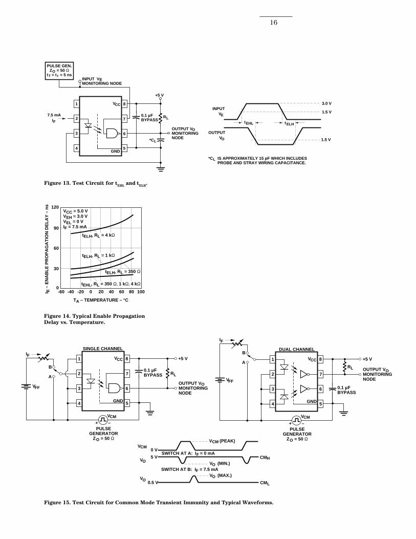
16
OUTPUT V MONITORING NODE
O
1.5 V
tEHL tELH
VE
INPUT
OVOUTPUT
3.0 V
1.5 V
+5 V
7
5
6
8
2
3
4
1
PULSE GEN.Z = 50 Ω
t = t = 5 nsO
f
IFLR
CCV
0.1 µFBYPASS
*CL
*C IS APPROXIMATELY 15 pF WHICH INCLUDES PROBE AND STRAY WIRING CAPACITANCE.
L
GND
r
7.5 mA
INPUT VEMONITORING NODE
Figure 13. Test Circuit for tEHL and tELH.
Figure 14. Typical Enable PropagationDelay vs. Temperature.
Figure 15. Test Circuit for Common Mode Transient Immunity and Typical Waveforms.
VO 0.5 V
OV (MIN.)5 V
0 VSWITCH AT A: I = 0 mAF
SWITCH AT B: I = 7.5 mAF
CMV
HCM
CML
OV (MAX.)
CMV (PEAK)
VO
t E –
EN
AB
LE
PR
OP
AG
AT
ION
DE
LA
Y –
ns
-600
TA – TEMPERATURE – °C
100
90
120
-20
30
20 60-40 0 40 80
60
VCC = 5.0 VVEH = 3.0 VVEL = 0 VIF = 7.5 mA
tELH, RL = 4 kΩ
tELH, RL = 1 kΩ
tEHL, RL = 350 Ω, 1 kΩ, 4 kΩ
tELH, RL = 350 Ω
+5 V
7
5
6
8
2
3
4
1 CCV
0.1 µFBYPASS
GND
OUTPUT V MONITORING NODE
O
PULSEGENERATOR
Z = 50 ΩO
+
IF
B
A
VFF
CMV
–
RL
SINGLE CHANNEL
+5 V
7
5
6
8
2
3
4
1 CCV
0.1 µFBYPASS
GND
OUTPUT V MONITORING NODE
O
PULSEGENERATOR
Z = 50 ΩO
+
IF
B
A
VFF
CMV
–
RL
DUAL CHANNEL
17
Figure 16. Thermal Derating Curve, Dependence of Safety Limiting Value withCase Temperature per IEC/EN/DIN EN 60747-5-2.
Figure 17. Recommended Printed Circuit Board Layout.
OU
TP
UT
PO
WE
R –
PS
, IN
PU
T C
UR
RE
NT
– I S
00
TS – CASE TEMPERATURE – °C
17550
400
12525 75 100 150
600
800
200
100
300
500
700
PS (mW)
IS (mA)
HCNWXXXX
GND BUS (BACK)
VCC BUS (FRONT)
ENABLE
0.1µF
10 mm MAX.(SEE NOTE 5)
OUTPUT
NC
NC
SINGLE CHANNELDEVICE ILLUSTRATED.
OU
TP
UT
PO
WE
R –
PS
, IN
PU
T C
UR
RE
NT
– I S
00
TS – CASE TEMPERATURE – °C
20050
400
12525 75 100 150
600
800
200
100
300
500
700PS (mW)
IS (mA)
HCPL-2611 OPTION 060
175
18
VCC15 V
GND 1
D1*
SHIELD
DUAL CHANNEL DEVICECHANNEL 1 SHOWN
8
7
5
390 Ω
0.1 µFBYPASS
1
2
+
–
5 V
GND 2
VCC2
2
470 Ω
1
IF
VF
*DIODE D1 (1N916 OR EQUIVALENT) IS NOT REQUIRED FOR UNITS WITH OPEN COLLECTOR OUTPUT.
VCC15 V
GND 1
D1*
IF
VF
SHIELD
SINGLE CHANNEL DEVICE
8
6
5
390 Ω
0.1 µFBYPASS
2
3
+
–
5 V
GND 2
VCC2
2
470 Ω
17VE
Figure 18. Recommended TTL/LSTTL to TTL/LSTTL Interface Circuit.

19
Propagation Delay, Pulse-Width Distortion andPropagation Delay SkewPropagation delay is a figure ofmerit which describes howquickly a logic signal propagatesthrough a system. The propaga-tion delay from low to high (tPLH)is the amount of time required foran input signal to propagate tothe output, causing the output tochange from low to high.Similarly, the propagation delayfrom high to low (tPHL) is theamount of time required for theinput signal to propagate to theoutput causing the output tochange from high to low (seeFigure 8).
Pulse-width distortion (PWD)results when tPLH and tPHL differ invalue. PWD is defined as thedifference between tPLH and tPHLand often determines themaximum data rate capability of atransmission system. PWD can beexpressed in percent by dividingthe PWD (in ns) by the minimumpulse width (in ns) beingtransmitted. Typically, PWD onthe order of 20-30% of theminimum pulse width is tolerable;the exact figure depends on theparticular application (RS232,RS422, T-l, etc.).
Propagation delay skew, tPSK, isan important parameter toconsider in parallel data applica-
tions where synchronization ofsignals on parallel data lines is aconcern. If the parallel data isbeing sent through a group ofoptocouplers, differences inpropagation delays will cause thedata to arrive at the outputs of theoptocouplers at different times. Ifthis difference in propagationdelays is large enough, it willdetermine the maximum rate atwhich parallel data can be sentthrough the optocouplers.
Propagation delay skew is definedas the difference between theminimum and maximumpropagation delays, either tPLH ortPHL, for any given group ofoptocouplers which are operatingunder the same conditions (i.e.,the same drive current, supplyvoltage, output load, andoperating temperature). Asillustrated in Figure 19, if theinputs of a group of optocouplersare switched either ON or OFF atthe same time, tPSK is thedifference between the shortestpropagation delay, either tPLH ortPHL, and the longest propagationdelay, either tPLH or tPHL.
As mentioned earlier, tPSK candetermine the maximum paralleldata transmission rate. Figure 20is the timing diagram of a typicalparallel data application with boththe clock and the data lines beingsent through optocouplers. Thefigure shows data and clock
signals at the inputs and outputsof the optocouplers. To obtain themaximum data transmission rate,both edges of the clock signal arebeing used to clock the data; ifonly one edge were used, theclock signal would need to betwice as fast.
Propagation delay skew repre-sents the uncertainty of where anedge might be after being sentthrough an optocoupler. Figure20 shows that there will beuncertainty in both the data andthe clock lines. It is importantthat these two areas of uncertaintynot overlap, otherwise the clocksignal might arrive before all ofthe data outputs have settled, orsome of the data outputs maystart to change before the clocksignal has arrived. From theseconsiderations, the absoluteminimum pulse width that can besent through optocouplers in aparallel application is twice tPSK. Acautious design should use aslightly longer pulse width toensure that any additionaluncertainty in the rest of thecircuit does not cause a problem.
The tPSK specified optocouplersoffer the advantages ofguaranteed specifications forpropagation delays, pulsewidthdistortion and propagation delayskew over the recommendedtemperature, input current, andpower supply ranges.
Figure 19. Illustration of PropagationDelay Skew - tPSK.
Figure 20. Parallel Data TransmissionExample.
50%
1.5 V
I F
VO
50%I F
VO
tPSK
1.5 V
DATA
t PSK
INPUTS
CLOCK
DATA
OUTPUTS
CLOCK
t PSK
www.agilent.com/semiconductorsFor product information and a complete list ofdistributors, please go to our web site.
For technical assistance call:
Americas/Canada: +1 (800) 235-0312 or(916) 788-6763
Europe: +49 (0) 6441 92460
China: 10800 650 0017
Hong Kong: (+65) 6756 2394
India, Australia, New Zealand: (+65) 6755 1939
Japan: (+81 3) 3335-8152 (Domestic/Interna-tional), or 0120-61-1280 (Domestic Only)
Korea: (+65) 6755 1989
Singapore, Malaysia, Vietnam, Thailand,Philippines, Indonesia: (+65) 6755 2044
Taiwan: (+65) 6755 1843
Data subject to change.Copyright © 2004 Agilent Technologies, Inc.Obsoletes 5989-0302ENDecember 29, 20045989-2126EN
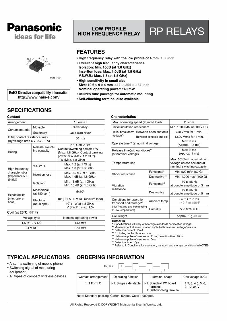
RP
SPECIFICATIONS
LOW PROFILE HIGH FREQUENCY RELAY RP RELAYS
mm inch
9.748
4.157
10.6.417
RoHS Directive compatibility informationhttp://www.nais-e.com/
FEATURES• High frequency relay with the low profile of 4 mm .157 inch• Excellent high frequency characteristics
Isolation: Min. 10dB (at 1.8 GHz)Insertion loss: Max. 1.0dB (at 1.8 GHz)V.S.W.R.: Max. 1.3 (at 1.8 GHz)
• High sensitivity in small sizeSize: 10.6 × 9 × 4 mm .417 × .354 × .157 inchNominal operating power: 140 mW
• Utilizes tube package for automatic mounting.• Self-clinching terminal also available
Arrangement
Contact materialMovable
Stationary
Nominal switch-ing capacity
V.S.W.R.
Insertion loss
Isolation
Mechanical(at 180 cpm)
Electrical(at 20 cpm)
Initial contact resistance, max.(By voltage drop 6 V DC 0.1 A)
Rating
High frequency characteristics(Impedance 50Ω)(Initial)
Expected life(min. opera-tions)
Contact
Coil (at 25°C, 68°F)
Voltage type
1.5 to 12 V DC
24 V DC
Nominal operating power
140 mW
270 mW
1 Form C
Silver alloy
Gold-clad silver
50 mΩ
0.1 A 30 V DCContact switching power: 1 W(Max. 1.8 GHz); Contact carryingpower: 3 W (Max. 1.2 GHz)1 W (Max. 1.8 GHz)
Max. 1.2 (at 1 GHz)Max. 1.3 (at 1.8 GHz)
Max. 0.5 dB (at 1 GHz)Max. 1 dB (at 1.8 GHz)
Min. 15 dB (at 1 GHz)Min. 10 dB (at 1.8 GHz)
5×10⁶
105 (0.1 A 30 V DC resistive load)
105 (1 W at 1.8 GHz; V.S.W.R.: max. 1.3)
Max. operating speed (at rated load)
Initial breakdown voltage*2
Initial insulation resistance*1
Operate time*3 (at nominal voltage)
Release time(without diode)*3
(at nominal voltage)
Temperature rise
Shock resistance
Vibration resistance
Unit weight
Remarks* Specifications will vary with foreign standards certification ratings.*1 Measurement at same location as “Initial breakdown voltage” section*2 Detection current: 10mA*3 Excluding contact bounce time*4 Half-wave pulse of sine wave: 11ms, detection time: 10µs*5 Half-wave pulse of sine wave: 6ms*6 Detection time: 10µs*7 Refer to 7. Conditions for operation, transport and storage conditions in NOTES
Approx. 1 g .04 oz
Characteristics
20 cpm
Min. 1,000 MΩ at 500 V DC
750 Vrms for 1 min.
1,500 Vrms for 1 min.
Between open contacts
Between contacts and coilMax. 3 ms
(Approx. 1.5 ms)
Max. 2 ms(Approx. 1 ms)
Max. 50°Cwith nominal coil voltage across coil and at nominal switching capacity
Min. 500 m/s2 50 G
Min. 1,000 m/s2 100 G
Functional*4
Destructive*5
Functional*6
Destructive
10 to 55 Hzat double amplitude of 3 mm
10 to 55 Hzat double amplitude of 5 mm
Conditions for operation,transport and storage*7
(Not freezing and condensing at low temperature)
Ambient temp.
Humidity
–40°C to 70°C –40°F to 158°F
5 to 85% R.H.
TYPICAL APPLICATIONS• Antenna switching of mobile phone• Switching signal of measuring
equipment• All types of compact wireless devices
ORDERING INFORMATION
1Ex. RP
Contact arrangement
1: 1 Form C
Note: Standard packing; Carton: 50 pcs. Case 1,000 pcs.
Nil: Single side stable 1.5, 3, 4.5, 5, 6, 9, 12, 24 V
Operating function
Nil:
H:
Standard PC board terminalSelf-clinching terminal
Terminal shape Coil voltage (DC)
All Rights Reserved © COPYRIGHT Matsushita Electric Works, Ltd.
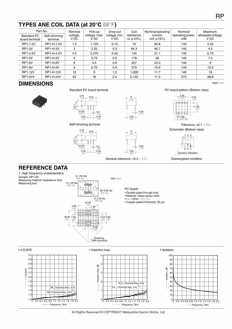
RPTYPES ANE COIL DATA (at 20°C 68°F)
DIMENSIONS mm inch
REFERENCE DATA
Part No. Nominal voltage, V DC
Pick-up voltage, max.
V DC
Drop-out voltage, min.
V DC
Coil resistance, Ω (±10%)
Nominal operating current,
mA (±10%)
Nominal operating power,
mW
Maximum. allowable voltage,
V DCStandard PC
board terminalSelf-clinching
terminal
RP1-1.5V RP1-H-1.5V 1.5 1.125 0.15 16 93.8 140 2.25
RP1-3V RP1-H-3V 3 2.25 0.3 64.3 46.7 140 4.5
RP1-4.5V RP1-H-4.5V 4.5 3.375 0.45 145 31.1 140 6.75
RP1-5V RP1-H-5V 5 3.75 0.5 178 28 140 7.5
RP1-6V RP1-H-6V 6 4.5 0.6 257 23.3 140 9
RP1-9V RP1-H-9V 9 6.75 0.9 579 15.6 140 13.5
RP1-12V RP1-H-12V 12 9 1.2 1,028 11.7 140 18
RP1-24V RP1-H-24V 24 18 2.4 2,133 11.3 270 28.8
Standard PC board terminal
Self-clinching terminal
General tolerance: ±0.3 ±.012
10.6.417
7.62.300
9.354
3.75.148
4.157
2.54.100
0.5.020
0.25.010
2.54.100
3.5.138
(0.25)(.010)
10.6.417
7.62.300
9.354
3.75.148
4.157
2.54.100
0.5.020
0.25.010
2.54.100
3.5.138
(0.25)(.010)
PC board pattern (Bottom view)
Tolerance: ±0.1 ±.004
Schematic (Bottom view)
Deenergized condition
5.08.200
7.62.300
6-1 dia.6-.039 dia.
2.54.100
6 5 4
1 2 3+ −
Direction indication
1. High frequency characteristicsSample: RP1-6VMeasuring method: Impedance 50ΩMeasuring tool:
6–1.60 dia.063 dia
6–1.00 dia.039 dia
6–2.30 dia.090 dia
26–0.80 dia.031 dia
18.92.7450.60
.0241.94.076
4.22.166
5.08.200
7.62.300
18.00.709
9.82.387
SolderingSMA connector
mm inch
PC board• Double-sided through hole• Material: Glass-epoxy resin• t = 1.0mm .039 inch• Copper plated thickness: 35 µm
• V.S.W.R • Insertion loss • Isolation
Frequency, GHz
0.80 0.4 1.0 1.81.61.41.20.60.2 2.0
1.2
1.4
1.8
2.0
2.2
2.6
3.0
1.6
2.4
2.8
1.0
NO (Terminal Nos. 5-6)
V.S
.W.R
.
NC (Terminal Nos. 4-5)1
2
3
4
5
0.80 0.4 1.00
1.81.61.41.20.60.2 2.0
Frequency, GHz
Inse
rtio
n lo
ss, d
B
N.O. (Terminal Nos. 5-6)
N.C. (Terminal Nos. 4-5)
10
20
40
50
60
80
100
0.80 0.4 1.0
30
70
90
01.81.61.41.20.60.2 2.0
Frequency, GHz
Isol
atio
n, d
B
All Rights Reserved © COPYRIGHT Matsushita Electric Works, Ltd.
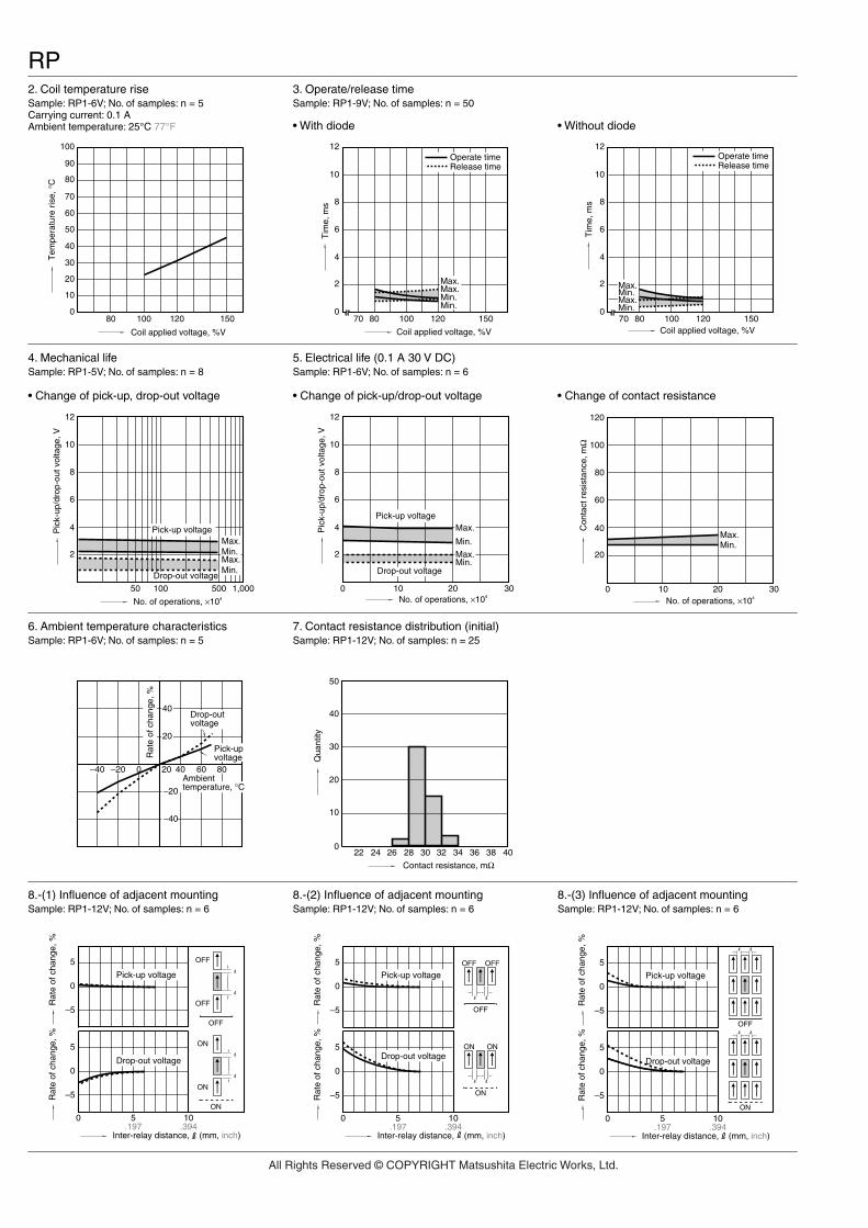
RP2. Coil temperature riseSample: RP1-6V; No. of samples: n = 5Carrying current: 0.1 AAmbient temperature: 25°C 77°F
3. Operate/release timeSample: RP1-9V; No. of samples: n = 50
• With diode • Without diode
10
30
60
70
80
100
80 100 120 1500
20
40
90
50
Coil applied voltage, %V
Tem
pera
ture
ris
e, °
C
2
4
6
8
10
12
70 80 100 120 1500
Max.Max.Min.Min.
Coil applied voltage, %VT
ime,
ms
Operate time Release time
2
4
6
8
10
12
70 80 100 120 1500
Max.Min.Max.Min.
Coil applied voltage, %V
Tim
e, m
s
Operate time Release time
4. Mechanical lifeSample: RP1-5V; No. of samples: n = 8
• Change of pick-up, drop-out voltage
5. Electrical life (0.1 A 30 V DC)Sample: RP1-6V; No. of samples: n = 6
• Change of pick-up/drop-out voltage • Change of contact resistance
2
4
6
8
10
12
100 1,00050050
Max.
Max.Min.
Min.
No. of operations, ×104
Pic
k-up
/dro
p-ou
t vol
tage
, V
Pick-up voltage
Drop-out voltage
2
4
6
8
10
12
3020100
Max.
Max.Min.
Min.
No. of operations, ×104
Pic
k-up
/dro
p-ou
t vol
tage
, V
Pick-up voltage
Drop-out voltage
20
40
60
80
100
120
3020100
Max.Min.
No. of operations, ×104
Con
tact
res
ista
nce,
mΩ
6. Ambient temperature characteristicsSample: RP1-6V; No. of samples: n = 5
7. Contact resistance distribution (initial)Sample: RP1-12V; No. of samples: n = 25
–40
40
20
–40 –20 0 20 40 60 80
Rat
e of
cha
nge,
%
Drop-outvoltage
Pick-upvoltage
Ambienttemperature, °C–20
10
20
40
50
2824 30
30
0383634322622 40
Contact resistance, mΩ
Qua
ntity
8.-(1) Influence of adjacent mountingSample: RP1-12V; No. of samples: n = 6
8.-(2) Influence of adjacent mountingSample: RP1-12V; No. of samples: n = 6
8.-(3) Influence of adjacent mountingSample: RP1-12V; No. of samples: n = 6
–5
10.394
5.197
0
0
5
–5
0
5 OFF
OFF
OFF
ON
ON
ON
Inter-relay distance, (mm, inch)
Rat
e of
cha
nge,
%R
ate
of c
hang
e, %
Pick-up voltage
Drop-out voltage
OFF OFF
OFF
ON ON
ON–5
10.394
5.197
0
0
5
–5
0
5
Inter-relay distance, (mm, inch)
Rat
e of
cha
nge,
%R
ate
of c
hang
e, %
Pick-up voltage
Drop-out voltage
OFF
ON
–5
10.394
5.197
0
0
5
–5
0
5
Inter-relay distance, (mm, inch)
Rat
e of
cha
nge,
%R
ate
of c
hang
e, %
Pick-up voltage
Drop-out voltage
All Rights Reserved © COPYRIGHT Matsushita Electric Works, Ltd.
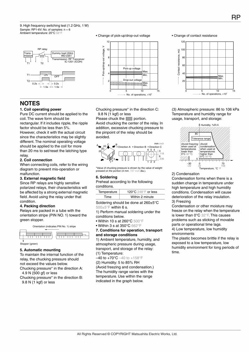
RP
NOTES
9. High frequency switching test (1.2 GHz, 1 W)Sample: RP1-6V; No. of samples: n = 6Ambient temperature: 20°C 68°F
• Change of pick-up/drop-out voltage • Change of contact resistance
T1 T2
T1
T20.2s 0.2s
1.5s 1.5s
OFF
Trans-mission
Dummy load (50Ω) WD-2351Transmission: RF Tranceiver IC-1201 (ICOH)
ON
RP relay
2
4
6
8
10
12
151050
Max.
Max.Min.
Min.
No. of operations, ×104
Pic
k-up
/dro
p-ou
t vol
tage
, V
Pick-up voltage
Drop-out voltage 20
40
60
80
100
120
151050
Max.Min.
No. of operations, ×104
Con
tact
res
ista
nce,
mΩ
1. Coil operating powerPure DC current should be applied to the coil. The wave form should be rectangular. If it includes ripple, the ripple factor should be less than 5%.However, check it with the actual circuit since the characteristics may be slightly different. The nominal operating voltage should be applied to the coil for more than 20 ms to set/reset the latching type relay.2. Coil connectionWhen connecting coils, refer to the wiring diagram to prevent mis-operation or malfunction.3. External magnetic fieldSince RP relays are highly sensitive polarized relays, their characteristics will be affected by a strong external magnetic field. Avoid using the relay under that condition.4. Packing directionRelays are packed in a tube with the orientation stripe (PIN NO. 1) toward the green stopper.
5. Automatic mountingTo maintain the internal function of the relay, the chucking pressure should not exceed the values below.Chucking pressure* in the direction A: 4.9 N 500 gf or lessChucking pressure* in the direction B: 9.8 N 1 kgf or less
Chucking pressure* in the direction C: 9.8 N 1 kgf or lessPlease chuck the portion.Avoid chucking the center of the relay. In addition, excessive chucking pressure to the pinpoint of the relay should be avoided.
*Value of chucking pressure is shown by the value of weight pressed on the portion (4 mm .157 inch dia.).
6. SolderingPreheat according to the following conditions.
Soldering should be done at 260±5°C 500±5°F within 6 s.1) Perform manual soldering under the conditions below.• Within 10 s at 260°C 500°F• Within 3 s at 350°C 662°F7. Conditions for operation, transport and storage conditions1) Ambient temperature, humidity, and atmospheric pressure during usage, transport, and storage of the relay:(1) Temperature:–40 to +70°C –40 to +158°F(2) Humidity: 5 to 85% RH(Avoid freezing and condensation.)The humidity range varies with the temperature. Use within the range indicated in the graph below.
(3) Atmospheric pressure: 86 to 106 kPa Temperature and humidity range for usage, transport, and storage:
2) CondensationCondensation forms when there is a sudden change in temperature under high temperature and high humidity conditions. Condensation will cause deterioration of the relay insulation.3) FreezingCondensation or other moisture may freeze on the relay when the temperature is lower than 0°C 32°F. This causes problems such as sticking of movable parts or operational time lags.4) Low temperature, low humidity environmentsThe plastic becomes brittle if the relay is exposed to a low temperature, low humidity environment for long periods of time.
Orientation (indicates PIN No. 1) stripe
Stopper (green)
Temperature 120°C 248°F or less
Time Within 2 minute
A C B• Direction A • Direction B • Direction C
mm inch
5 46
2 3
3.1186.236
11 23
(4)(5)
(6)
Temperature, °C °F
85
5
032
70158
–30–22
(Avoidcondensationwhen used attemperatureshigher than0°C 32°F)
Humidity, %R.H.
Tolerance range
(Avoid freezingwhen used attemperatureslower than0°C 32°F)
All Rights Reserved © COPYRIGHT Matsushita Electric Works, Ltd.