Embed Size (px)
Citation preview
N°: 2009 ENAM XXXX
Télécom ParisTech Grande école de l’Institut Télécom – membre fondateur de ParisTech
46, rue Barrault – 75634 Paris Cedex 13 – Tél. + 33 (0)1 45 81 77 77 – www.telecom-paristech.fr
T
H
E
S
2012-ENST-027
Présenté et soutenue publiquement par
Islam SEOUDI
5 juin 2012
Multi-electrode System Design and Optimization for Cardiac Implants
Doctorat ParisTech
T H È S E
Pour obtenir le grade de docteur délivré par
Télécom ParisTech
Spécialité “Electronique et Communications”
Directeur de thèse : Amara AMARA
T
H
È
S
E
Jury
M. Marc Belleville, Chief Scientist, CEA-Leti RAPPORTEUR
M. Jean-Michel PORTAL, Professeur, Ecole Polytechnique Universitaire de Marseille RAPPORTEUR
M. Christian PIGUET, Professeur, CSEM EXAMINATEUR
Mme Lirida NAVINER, Professeur, Telecom ParisTech EXAMINATEUR
M. Alain RIPART, Vice-President, Sorin CRM EXAMINATEUR
M. Daniel KROISS, Vice-President & Chief Scientific Officer, Sorin CRM INVITE
M. Amara AMARA, Directeur de Recherche, ISEP DIRECTEUR DE THESE
Mme Karima AMARA, Ingénieur Project, Sorin CRM CO-DIRECTEUR DE THESE
Title: Multi-Electrode System Design and Optimization for Cardiac Implants
Abstract: Cardiac implants like ICD (Implantable Cardioverter Defibrillator) are life saving devices
in cases of sudden cardiac arrhythmias. In other conditions like the one of heart failure, cardiac implants like CRT (Cardiac Rhythm Therapy) are prescribed to restore the coordinated contraction of the heart. Such treatment consists of the delivery of localized electrical stimuli to the cardiac tissue via electrodes in the stimulation lead. Conventionally the stimulation lead come either in unipolar or bipolar configuration (1 or 2 electrode) which have been found to be sufficient for pacing the right atrium and right ventricle, studies have shown the benefits of a multi-electrode system for pacing left ventricle essential for cardiac resynchronization. This thesis discusses the design and optimization of a multi-electrode system capable of alleviating the limitations and constraints related to left ventricular stimulation. We first present a chip implementation of such multi-electrode system. It was taped out in 0.18 µm technology and occupies 2.25x5.35 mm² area . The chip also features a specially designed communication protocol and is compliant with the existing standards. It enables low power operation and allows quick configuration. Thereafter we present the design and implementation of a default connection unit (DCU) to ensure the compatibility of our multi-electrode lead with pacemakers not designed specifically to control such a lead. Like the multi-electrode chip the DCU unit was taped out in 0.18 µm technology, occupies 2.2 x 1.75 mm² area and harvests the stimulation energy to power itself. Finally we present a proof of concept study for the adaptation and integration of non-volatile memory technologies within the multi-electrode system. New technologies were explored which drastically improve the performance of the multi-electrode system. The employment of such technologies enhanced our multi-electrode system by eliminating the need of repetitive configuration of electrodes, thereby saving power and reducing latency. The benefits also included smaller area and compatibility with any pacemaker in the market. Through simulations we proved the feasibility of these technologies for our implant applications.
Keywords : Cardiac pacemakers, multi-electrode, stimulation, medical implants, switching, MOS,
non-volatile, memories
Titre : Conception et Optimisation de Système Multi-électrodes Pour Les Implants Cardiaques
Résumé: Les implants cardiaques tels que les défibrillateurs implantables sont des appareils
permettant de sauver la vie dans le cas de troubles de l’arythmie cardiaque soudaine. Tandis que dans le cas des attaques cardiaques, les implants CRT sont utilisés pour rétablir la cadence de la contraction cardiaque. De tels traitements consistent en l’application de stimulations locales au tissue cardiaque via des électrodes se trouvant dans les sondes de stimulation. Ces dernières se présentent soit dans une configuration unipolaire ou bipolaire ; qui ont prouvé leur efficacité pour stimuler le ventricule droit et l’oreillette droite ; des études ont montré l’efficacité de la sonde multi-électrode dans la stimulation du ventricule gauche indispensable pour la resynchronisation cardiaque. Cette thèse traite de la conception et l’optimisation d’un système multi-électrodes capable d’éviter les limitations et les contraintes liées à la stimulation du ventricule gauche. Tout d’abord, une réalisation de ce système cette est présentée et fabriqué dans une technologie 0.18 µm. Le circuit a également un protocole de communication spécifique. Il permet une opération basse consommation et une configuration rapide. Ensuite, la conception et la réalisation d’une unité de configuration par default est présentée. Cette unité assure la compatibilité de notre sonde avec les stimulateurs cardiaques du marché. Finalement, une étude pour l’adaptation et l’intégration des technologies mémoire non-volatile dans la sonde est présentée. De telles technologies améliorent considérablement le système en évitant le besoin de reconfiguration des sondes et en conséquence réduire la latence et la consommation.
Mots clés: implants cardiaques, pacemaker, multi-électrodes, sondes, switching, MOS,
mémoires non volatile

4

5
Acknowledgment I would like to thank Mr. Renzo Dal Molin for this exceptional opportunity to work with him at the
Advanced Research Department of Sorin Group from where this thesis work started. I would like to
thank Professor Amara for accepting me as his student for which I’m grateful. I was lucky enough to
have Professor Amara as my PhD director. He gave the example how an advisor can be as a father
for his student, offers him unlimited support without counting, and lighting the dark paths full of
doubts and unclear ideas.
I am grateful to Karima Amara for revealing all the secrets of digital electronics design for me. She
also taught me how to insist and dig after the promising ideas and to be equipped with patience in
order to convert them into meaningful inventions. I am also grateful to Jean-Francois Debroux and
Marc Laflutte for revealing all the secrets of analog electronics design for me and for their
unquestionable support and sincere advice.
I will strongly remember Alaa Makdissi with his rich scientific discussions and his enormous
capacity to retrieve solutions for persistent problems. I want to thank him for his sincere advice and
support.
All my thanks and gratitude I would present them to my friend Ashutosh who gave a perfect
example for how a friend can support sincerely and generously his friend. When talking about
generosity, I cannot forget Balwant Godara for being so kind, helpful and generous in giving me
advice.
I would like to thank all my colleagues with whom I enjoyed to work:
Sir Julien Ardelean, Sebastien Jackard and all the “advanced research”, Fabrice Gayral, Bruno Eon,
Jean-Claude Bierg, Didier Gourgousse, Jean-Pierre Noel, Jean-Yves and all the R&D, Bruno, Adel,
Etienne, Wen, Nabil and all V&V, Emmanuel Bigen and all System design at Sorin.
I am also grateful to Francis Chan Wai Po, Costin Anghel, Andrei Vladimirescu and wish all the best
for Hraziia, Rutwick, Adam and Khaja in their Phd.
In such special moments, special persons are always remembered because without them I wouldn’t
have reached this achievement today. To my father Zakaria and my mother Elham I owe them this
achievement and nothing can be presented to them in return other than an eternal thanks and
gratitude.
To my wife Salma I present my gratitude for her support in many difficult periods of this thesis and
for always pushing me forward to reach my goals.
To my brothers Yahia, Ahmed and Nour: thanks for your continuous support and for urging me
constantly towards higher achievements and bigger success.
To all my Seoudi and Hammouda families I dedicate this work.

6

7
Contents
8
Acknowledgment 5
Contents 7
List of Figures 12
List of Tables 15
Résumé de la thèse en Français 17
Chapitre 1: Introduction 18
Chapitre 2: Les Implants de Stimulation Cardiaque 21
Système de stimulation cardiaque implantable 22
Thérapie de resynchronisation cardiaque (CRT) 23
Chapitre 3: Système Multi-Electrodes Pour La Stimulation Ventriculaire Gauche: Conception et
Mise en Œuvre 25
Système Multi-Electrode : Principe & Contraintes 25
Conception et implémentation du système 26
Résultat de Mesure 31
Chapitre 4: Unité de Connexion Par Défaut 32
Les choix et défies de conception 33
Le Principe de l’opération du DCU 34
Résultats 35
Chapitre 5 : L'Amélioration de la Sonde Multi-Electrode en Utilisant La Technologie des
Mémoires Non-Volatiles 35
1 Chapter 1 40
2 Chapter 2 44
2.1 Introduction 46
2.2 Human Heart and Cardiac Implant Evolution 46
2.2.1 Heart failure condition 48
2.2.2 Arrhythmias 48
2.2.3 First Implantable pacemaker 48
2.2.4 Demand Pacemaker 49
9
2.2.5 Rate-Responsive Pacemaker 49
2.3 Implantable Cardiac Stimulation System 49
2.3.1 Pulse Generator (Implant - CAN) 51
2.3.1.1 Power source 51
2.3.1.2 Output circuit 52
2.3.1.3 Sensing Unit 56
2.3.1.4 Control unit 58
2.3.2 Leads 59
2.3.2.1 Unipolar 60
2.3.2.2 Bipolar 60
2.4 Cardiac Resynchronization Therapy (CRT) 61
2.4.1 Phrenic nerve stimulation 62
2.4.2 Limited choice of stimulation site 62
2.4.3 Lead displacement 62
2.5 Conclusion 63
References 64
3 Chapter 3 66
3.1 Introduction 68
3.2 Multi-electrode System: Principle & Constraints 69
3.1.1 Compliance with standards 70
3.1.2 Communication protocol: Power and Configuration 71
3.3 State of the Art 71
3.3.1 Implementation Strategies for LEC 72
3.3.1.1 Centralized Structure 72
3.3.1.2 Distributed Structure 73
3.3.1.3 Direct Structure 74
3.4 System Design & Implementation 74
3.4.1 Adopted Strategy 74
3.4.2 Implant and lead electrode controller (IEC & LEC) 75
3.4.2.1 Power Storage Unit 77
10
3.4.2.2 Control Unit 78
3.4.2.3 Oscillators 78
3.4.2.4 OTP Memory 79
3.4.2.5 Main Switching Unit 79
3.4.2.6 Auxiliary Switching Unit 79
3.4.2.7 Charge Pump 80
3.4.3 Communication Protocol 80
3.4.3.1 Power pulses 83
3.4.3.2 Event Synchronization bits 83
3.4.3.3 Configuration bits 83
3.4.3.4 Double Stimulation 87
3.4.4 Comparison 88
3.5 Distributed Structure 88
3.6 Measurement Results 89
3.7 Conclusion 92
Publications 93
References 93
4 Chapter 4 95
4.1 Introduction 97
4.2 Design Challenges and Choices 98
4.3 DCU Operation Principle 100
4.4 System Implementation 100
4.4.1 Architecture 100
4.4.2 MOS Sizing 105
4.4.3 Gate capacitance sizing 106
4.4.4 Noise 107
4.5 Results 107
4.6 Conclusion 110
Publications 111
References 111
11
5 Chapter 5 113
5.1 Introduction 115
5.2 Enhancements to the Multi-Electrode 115
5.3 Advanced Non-Volatile Memory Technologies 117
5.3.1 Nanotube RAM (NRAM) 117
5.3.1.1 NRAM Application for Multi-Electrode Switching Unit 120
5.3.2 Resistive RAM family 122
5.3.1.1 Magnetic Tunnel Junction (MTJ) 122
5.3.1.2 Memristance 128
5.3.1.3 Memristance Behabioral Model 130
5.3.1.4 Adapting Memristance Cell for Cardiac Stimulation applications 132
5.2 Conventional Non-Volatile Memory Technology: Flash Memory 137
5.2.1 Theoretical background 137
5.2.2 Flash cell model 139
5.2.2.1 Program Sequence using Channel Hot Electron Method 139
5.2.2.2 ERASE Sequence using Fowler Nordheim Injection method 141
5.2.2.3 Observed Characteristics of the Flash Cell 142
5.2.2.4 Operation Window expansion to adapt with our application 142
5.2.2.5 Evolution of VT with QFG0 (simulation) 143
5.2.3 Non-Volatile Switching Unit Using Flash Memory Cell 144
4.3.1 Case 1: MOS Switch connects Cathode to Electrode 146
Case 2: MOS Switch connects Anode to Electrode 148
5.2.4 Summary 151
5.3 Conclusion 153
Publications 153
References 154
6 Chapter 6 157
List of Publications 161
12
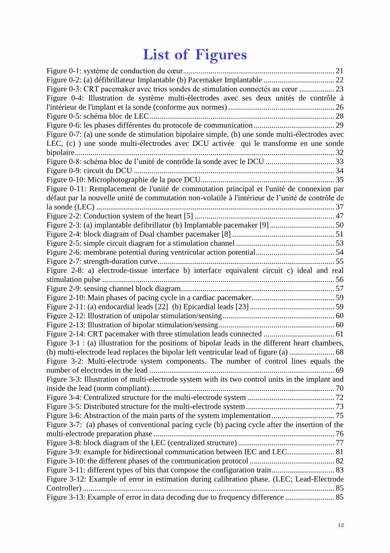
List of Figures Figure 0-1: système de conduction du cœur ............................................................................. 21 Figure 0-2: (a) défibrillateur Implantable (b) Pacemaker Implantable .................................... 22 Figure 0-3: CRT pacemaker avec trios sondes de stimulation connectés au cœur .................. 23 Figure 0-4: Illustration de système multi-électrodes avec ses deux unités de contrôle à
l'intérieur de l'implant et la sonde (conforme aux normes) ...................................................... 26
Figure 0-5: schéma bloc de LEC .............................................................................................. 28 Figure 0-6: les phases différentes du protocole de communication ......................................... 29 Figure 0-7: (a) une sonde de stimulation bipolaire simple, (b) une sonde multi-électrodes avec
LEC, (c) ) une sonde multi-électrodes avec DCU activée qui le transforme en une sonde
bipolaire .................................................................................................................................... 32
Figure 0-8: schéma bloc de l’unité de contrôde la sonde avec le DCU ................................... 33
Figure 0-9: circuit du DCU ...................................................................................................... 34
Figure 0-10: Microphotographie de la puce DCU.................................................................... 35 Figure 0-11: Remplacement de l'unité de commutation principal et l'unité de connexion par
défaut par la nouvelle unité de commutation non-volatile à l'intérieur de l’unité de contrôle de
la sonde (LEC) ......................................................................................................................... 37
Figure 2-2: Conduction system of the heart [5] ....................................................................... 47 Figure 2-3: (a) implantable defibrillator (b) Implantable pacemaker [9] ................................. 50 Figure 2-4: block diagram of Dual chamber pacemaker [8] .................................................... 51
Figure 2-5: simple circuit diagram for a stimulation channel .................................................. 53 Figure 2-6: membrane potential during ventricular action potential ........................................ 54
Figure 2-7: strength-duration curve .......................................................................................... 55 Figure 2-8: a) electrode-tissue interface b) interface equivalent circuit c) ideal and real
stimulation pulse ...................................................................................................................... 56
Figure 2-9: sensing channel block diagram .............................................................................. 57
Figure 2-10: Main phases of pacing cycle in a cardiac pacemaker .......................................... 59 Figure 2-11: (a) endocardial leads [22] (b) Epicardial leads [23] ........................................... 59 Figure 2-12: Illustration of unipolar stimulation/sensing ......................................................... 60
Figure 2-13: Illustration of bipolar stimulation/sensing ........................................................... 60 Figure 2-14: CRT pacemaker with three stimulation leads connected .................................... 61
Figure 3-1 : (a) illustration for the positions of bipolar leads in the different heart chambers,
(b) multi-electrode lead replaces the bipolar left ventricular lead of figure (a) ....................... 68 Figure 3-2: Multi-electrode system components. The number of control lines equals the
number of electrodes in the lead .............................................................................................. 69 Figure 3-3: Illustration of multi-electrode system with its two control units in the implant and
inside the lead (norm compliant) .............................................................................................. 70
Figure 3-4: Centralized structure for the multi-electrode system ............................................ 72
Figure 3-5: Distributed structure for the multi-electrode system ............................................. 73 Figure 3-6: Abstraction of the main parts of the system implementation ................................ 75 Figure 3-7: (a) phases of conventional pacing cycle (b) pacing cycle after the insertion of the
multi-electrode preparation phase ............................................................................................ 76 Figure 3-8: block diagram of the LEC (centralized structure) ................................................. 77
Figure 3-9: example for bidirectional communication between IEC and LEC ........................ 81 Figure 3-10: the different phases of the communication protocol ........................................... 82 Figure 3-11: different types of bits that compose the configuration train ................................ 83 Figure 3-12: Example of error in estimation during calibration phase. (LEC; Lead-Electrode
Controller) ................................................................................................................................ 85 Figure 3-13: Example of error in data decoding due to frequency difference ......................... 85
13
Figure 3-14:Biphasic stimulation pulses as an example of double stimulation mode ............. 87
Figure 3-15: Block diagram of multi-electrode system (distributed structure) ........................ 89 Figure 3-16: LEC chip microphotograph ................................................................................. 90 Figure 3-17: Errors in decoding before and after the application of our communication
protocol ..................................................................................................................................... 91 Figure 3-18: signal on P&C line as observed during chip validation ...................................... 91 Figure 4-1: (a) Simple bipolar stimulation lead, (b) Multi-electrode stimulation lead with an
electrode-controller LEC, (c) Multi-electrode stimulation lead with the DCU activated
resulting in a bipolar lead ......................................................................................................... 97
Figure 4-2: Lead Electrode Controller blockdiagram including the DCU ............................... 99 Figure 4-3: DCU circuit ......................................................................................................... 101 Figure 4-4: MAX-MIN generator circuit ............................................................................... 102 Figure 4-5: circuit and symbol of S1 switch .......................................................................... 103
Figure 4-6: Circuit and symbol of S2 switch ......................................................................... 103 Figure 4-7: Simulation results of DCU in its active state ...................................................... 108 Figure 4-8: Simulation results of DCU in its inactive state ................................................... 108
Figure 4-9: DCU chip microphotograph ................................................................................ 109 Figure 5-1: Replacement of main switching unit and default connection unit by the new non-
volatile switching unit inside the lead electrode-controller unit ............................................ 116 Figure 5-2: single walled carbon nanotube [18] ..................................................................... 117
Figure 5-3: NRAM cell in erased state (left) Programmed state (right) [24] ........................ 118 Figure 5-4: measured values for ON/OFF resistances (left), measured voltages and currents
(right) [16] .............................................................................................................................. 119
Figure 5-5: An example for the non-volatile switching unit in the multi-electrode system .. 120 Figure 5-6: MTJ states [2] ...................................................................................................... 122
Figure 5-7: FIMS cell (a) read phase (b) write phase [13] ..................................................... 123
Figure 5-8: toggle cell anatomy - SAF layers [17, 18] ........................................................... 124
Figure 5-9: toggle sequence ................................................................................................... 125 Figure 5-10: STT structure [2] ............................................................................................... 126
Figure 5-11: Memristance model ........................................................................................... 128 Figure 5-12: Memristance Voltage and current curves .......................................................... 129 Figure 5-13: (a) memristance symbol (b) behavioral model circuit in LT Spice ................. 130
Figure 5-14: (upper pane) input voltage sine wave of amplitude 1V and 0.5 Hz frequency
against the measured current across the cell. (lower pane) the variation of state variable w
with the input voltage ............................................................................................................. 131 Figure 5-15: plot of voltage against current presented in the upper pane of fig. 5-14. The result
is the double hysteresis curve ................................................................................................. 131
Figure 5-16: effect of increasing the full length D of the model on the double hysteresis curve
(behavior) ............................................................................................................................... 132 Figure 5-17: recheck of model correct behavior at all the voltage range after increasing D to
28nm ....................................................................................................................................... 133
Figure 5-18: model’s resistance evolution with an applied positive ramp voltage signal. .... 133 Figure 5-19: model’s resistance evolution with an applied negative ramp voltage signal. ... 134 Figure 5-20: Memristance model switching delay for different positive voltage applied across
the cell .................................................................................................................................... 135 Figure 5-21: (upper pane) applied positive voltage pulse sequence and the memristance cell
resistance is plotted. (lower pane) the measured current across the cell in the two directions.
The missing part of the current waveform signifies a stable current value ............................ 136 Figure 5-22: Flash memory cell showing the structure of its floating gate transistor [20] .... 137 Figure 5-23: Programming window of flash cell [20] ............................................................ 137

14
Figure 5-24: symbol for the generated flash cell - Program sequence ................................... 139
Figure 5-25: Program sequence waveforms for reference VerilogA Flash cell ..................... 140 Figure 5-26: Program sequence waveforms for the generated symbol of Flash cell ............. 140 Figure 5-27: Symbol for the generated flash cell - Erase sequence ....................................... 141
Figure 5-28: Erase sequence waveforms of reference VerilogA Flash cell ........................... 141 Figure 5-29: Erase sequence waveforms for the generated symbol of Flash cell .................. 142 Figure 5-30: (a) default operation window of the flash cell model, (b) application adapted
operation window of the model .............................................................................................. 143 Figure 5-31: Threshold voltage change with varying QFG0 @Vtuv = 1V............................ 144
Figure 5-32: concept schematic .............................................................................................. 145 Figure 5-33: Flash cell erased (ON) to block the connection between Cathode and Electrode1
................................................................................................................................................ 146 Figure 5-34:Flash cell programmed (off)to eneble the connection between Cathode and
Electrode1 ............................................................................................................................... 147 Figure 5-35: Flash cell is erased (ON) to enable the connection between Anode and
Electrode1 ............................................................................................................................... 148
Figure 5-36: Flash cell is programmed to block the connection between Anode and Electrode1
................................................................................................................................................ 150 Figure 5-37: A. Electrode = Cathode, B. Electrode = Anode, C. Electrode = not connected
151
Figure 5-38: example of complete system ............................................................................. 152
15
List of Tables
Table 0-1: Charecterictiques de la puce ................................................................................... 31 Table 2-1: normalized values for stimulation energy [11] ....................................................... 52 Table 2-2: parameters of stimulation channel .......................................................................... 53 Table 3-1: Bipolar lead vs. Multi-electrode lead ...................................................................... 69 Table 3-2: comparison of our solution with other multi-electrode systems found in patents .. 88
Table 3-3: Chip Summary ........................................................................................................ 90 Table 4-1: Operation modes ..................................................................................................... 99 Table 4-2: example for MOS sizing ....................................................................................... 105 Table 4-3: example of capacitance sizing .............................................................................. 106 Table 4-4: Chip Summary ...................................................................................................... 107
Table 5-1: switching unit specification for cardiac stimulation ............................................. 117 Table 5-2: NRAM features summary [19, 22] ....................................................................... 119 Table 5-3: STT features .......................................................................................................... 127
Table 5-4: Memristance model parameters [19] .................................................................... 132 Table 5-5: typical bias voltages for flash cell [23] ................................................................. 138 Table 5-6: Characteristics summary ....................................................................................... 142
Table 5-7: QFG0 = 0 and VT = 1V ....................................................................................... 147
Table 5-8: QFG0 = -8.5e-16 and VT = 9.07V ...................................................................... 148
Table 5-9: QFG0 = 0 and VT = 1V ...................................................................................... 149
Table 5-10: QFG0 = -8.5e-16 and VT = 9.07V .................................................................... 150

Résumé de la thèse en Français
16

Résumé de la thèse en Français
17
Résumé de la thèse en Français
Résumé de la thèse en Français
18
Chapitre 1: Introduction
Au cours des dernières années, la qualité des soins s’est beaucoup améliorée. Grace à la recherche
dans le domaine de la santé, aux nouvelles découvertes technologiques, les êtres humains vivent non
seulement plus longtemps, mais les thérapies suivies sont également de meilleure qualité ; elles
réduisent les chances de progression des maladies et permettent leur diagnostique de manière plus
précoce. Toutefois, il est important de noter que, malgré ces progrès, il est nécessaire de continuer
les efforts de recherche afin de faire face à des pathologies telles que celles liées à des complications
cardio-vasculaires qui affectent une grande partie de la population.
Dans plusieurs études, on estime que les maladies cardiovasculaires sont la cause principale de décès,
en particulier dans les sociétés industrielles avancées. Aux États-Unis les maladies cardio-vasculaires
sont la première cause de décès. Dans le monde entier, on estime à environ 40% le taux de décès
résultant de complications cardiaques.
Dans cette thèse, nous nous pencherons sur les implants cardiaques utilisés dans le traitement
cardio-vasculaire, en particulier les stimulateurs cardiaques et les défibrillateurs. Nous nous
pencherons sur la description de base de ces appareils d’un point de vue électronique et nous allons
également présenter leurs évolutions. En outre, nous présenterons nos résultats de recherche qui
contribuent tant à l'amélioration de la fonctionnalité qu’à l’augmentation de l’efficacité de ces
dispositifs en terme de volume, de performances et de consommation en puissance. Le plan de cette
thèse est le suivant:
Au chapitre 2, nous présentons le fonctionnement de base du cœur, les maladies cardio-vasculaires
importantes et les dispositifs utilisés pour gérer ces maladies. Nous détaillons l'évolution des
implants cardiaques et de leurs composants de base. Par la suite, nous analysons en détail
l’insuffisance cardiaque, une des maladies cardio-vasculaires les plus répandues. Par ailleurs, nous
discutons de la stimulation bi-ventriculaire qui est le mécanisme utilisé pour gérer l'insuffisance
cardiaque.
Au chapitre 3, nous présentons un système multi-électrodes pour résoudre le problème de la
stimulation bi-ventriculaire. Nous présentons les défis de conception, la méthodologie de conception
et les contraintes d'un tel système. Nous détaillons également les solutions existantes et leurs limites.
Enfin, nous présentons les performances et les résultats du système qui a été conçu.
Résumé de la thèse en Français
19
Au chapitre 4, nous détaillons la conception d'un bloc supplémentaire du système multi-électrodes
que nous avons présenté dans le chapitre 3. L'ajout de ce bloc à notre sonde multi-électrodes permet
de résoudre le problème de la compatibilité de notre système avec les stimulateurs cardiaques
existants. Nous présentons en détail la méthodologie de conception, les contraintes et les
performances de ce système.
Au chapitre 5, nous examinons les nouvelles technologies au-delà du CMOS standard, visant à
rendre notre sonde multi-électrodes plus intelligente, plus petite et plus performante. Nous
présentons plusieurs technologies candidates qui peuvent être utilisées dans notre système. Nous
discutons de leurs points forts, leurs points faiblesses. Finalement, au travers de simulations nous
démontrons la faisabilité de l’utilisation de certaines de ces technologies dans le cadre de l’application
visée.
Les principales contributions de cette thèse sont les suivants:
Conception et mise en œuvre d'un système multi-électrodes: Nous avons conçu et mis en œuvre
un système multi-électrodes qui est capable de stimuler plusieurs sites dans la chambre cardiaque.
Notre solution est entièrement configurable et répond aux contraintes de taille et de consommation
en puissance imposée par la nature de notre application. Notre puce a été fabriquée en technologie
0,18 µm et occupe 2.25x5.35 mm ². La puce, conforme aux normes en vigueur dans le domaine
médical, dispose également d'un protocole de communication dédié. Il permet un fonctionnement à
faible puissance et permet une configuration rapide. A notre connaissance, notre étude est la première
publiée dans son genre.
Conception et mise en œuvre de l'unité de connexion par défaut: Nous avons implémenté une
unité de connexion par défaut pour la puce multi-électrodes qui a permis l'exploitation de notre sonde
multi-électrodes par des stimulateurs cardiaques qui ne sont pas conçus spécifiquement pour le
contrôle de cette dernière. La solution élargit donc la compatibilité de notre sonde à tous les
stimulateurs cardiaques du marché. Dans ce chapitre, nous discutons et nous apportons des solutions
aux principaux défis liés à un environnement très contraignant comme celui du cœur humain. Cette
unité a été fabriquée en technologie 0,18 µm, elle occupe 2,2 x 1,75 mm ² de surface. Cette unité est
capable de récupérer l’énergie nécessaire de son fonctionnement depuis l’énergie de stimulation
envoyée au cœur.
Preuve de faisabilité de l’intégration des technologies de mémoire non volatile dans le
système multi-électrodes: De nouvelles technologies ont été explorées qui améliorent
Résumé de la thèse en Français
20
considérablement les performances du système multi-électrodes. L'emploi de ces technologies a
amélioré notre système en éliminant le besoin de configuration répétitive des électrodes, économisant
ainsi la consommation en puissance et réduisant la latence. Des avantages supplémentaires ont été
obtenus au niveau de la taille de la puce et sa compatibilité avec tout autre stimulateur sur le marché.
Nous avons exploré plusieurs technologies non volatiles, comme les NRAM, MRAM, Memristance
et Flash. Grâce aux simulations, nous avons prouvé la faisabilité de ces technologies pour nos
applications. Nous croyons que ces technologies seront utilisées pour concevoir la prochaine
génération des sondes à faible puissance et haute performance.
Résumé de la thèse en Français
21
Chapitre 2: Les Implants de Stimulation Cardiaque
Dans ce chapitre, on parle d’abord du fonctionnement de base du cœur et les disfonctionnements
possibles du système cardiovasculaire. Puis on parlera de l’évolution des implants cardiaques utilisés
dans le traitement de ces disfonctionnement ou maladies.
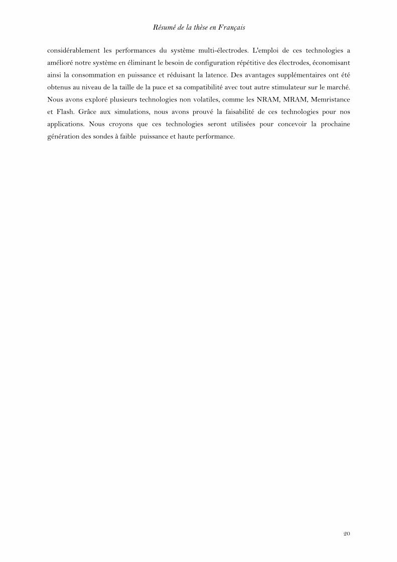
Figure 0-1: système de conduction du cœur
Le cœur humain et l’évolution de l’implant cardiaque
Le cœur est composé de quatre cavités, deux cavités reçoivent le sang désoxygéné de différentes
parties du corps, et deux cavités pompent le sang oxygéné de nouveau pour les parties du corps. Si
jamais la quantité de sang pompé par le cœur est diminuée pour une raison quelconque, cela pourrait
provoquer une perte de connaissance ou même la mort (l’insuffisance cardiaque).
Le fonctionnement du cœur est maintenu par un système de conduction électrique très complexe.
Toute activité électrique dans un cœur normal est initiée par le nœud sino-auriculaire connu comme
le pacemaker naturel du cœur. L’impulsion électrique se propage dans le système de conduction du
cœur comme illustré dans la figure 0-1. Toute perturbation dans ce système de conduction conduit à
une condition pathologique critique connue sous le nom d’arythmie.
Les implants cardiaques de nos jours offrent le traitement requis pour beaucoup de maladies comme
l’insuffisance cardiaque et la protection contre les situations potentiellement mortelles comme les
arythmies.
Le premier pacemaker implantable stimulait le cœur avec des impulsions électriques d’une largeur et
d’amplitude fixes à une fréquence fixée à 60 battements par minute. Ensuite, un nouveau concept a
été introduit par l’arrivée de ce qu’on appelle « On Demand Pacemaker » où l’activité du cœur est
Résumé de la thèse en Français
22
détectée grâce à un simple capteur dans le pacemaker et en fonction de cela, la stimulation adéquate
est générée. Cette nouveauté a contourné les inconvénients de la stimulation à fréquence fixe.
Avec la recherche permanente dans l'optimisation de la stimulation cardiaque en fonction des besoins
du patient, une étape supplémentaire a été franchie au-delà de la simple détection de l'activité
électrique du cœur du patient. Dans les années 1980, des capteurs plus intelligents ont été incorporés
dans le stimulateur cardiaque pour mesurer certains paramètres relatifs à l'activité physique du
patient tels que le mouvement du corps, la respiration et la pression artérielle
Système de stimulation cardiaque implantable
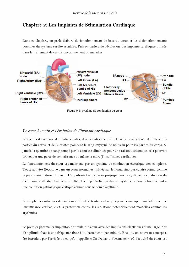
Les implants cardiaques sous ses deux déclinaisons – pacemaker ou défibrillateur - se composent
d’un générateur d’impulsion électrique implanté sous la peau de la poitrine. Ce générateur est
branché au cœur au moyen d’une sonde électriquement isolée de l’extérieur et insérée puis fixée à
l’intérieur de cœur (figure 0-2). Les sondes de stimulation sont équipées à leur extrémité par des
électrodes pour faire l’interface électrique avec les tissues cardiaques.
Figure 0-2: (a) défibrillateur Implantable (b) Pacemaker Implantable
Le nombre de sondes à insérer dans le cœur varie en fonction du nombre des cavités du cœur à
stimuler selon l’état du patient et la décision de son médecin. Soit une cavité (l’oreillette droite RA)
,soit deux cavités (l’oreillette droite RA et le ventricule droit RV) ou au maximum trois cavités en
ajoutant le ventricule gauche LV comme dans le cas de la thérapie de resynchronisation cardiaque
(CRT).
Résumé de la thèse en Français
23
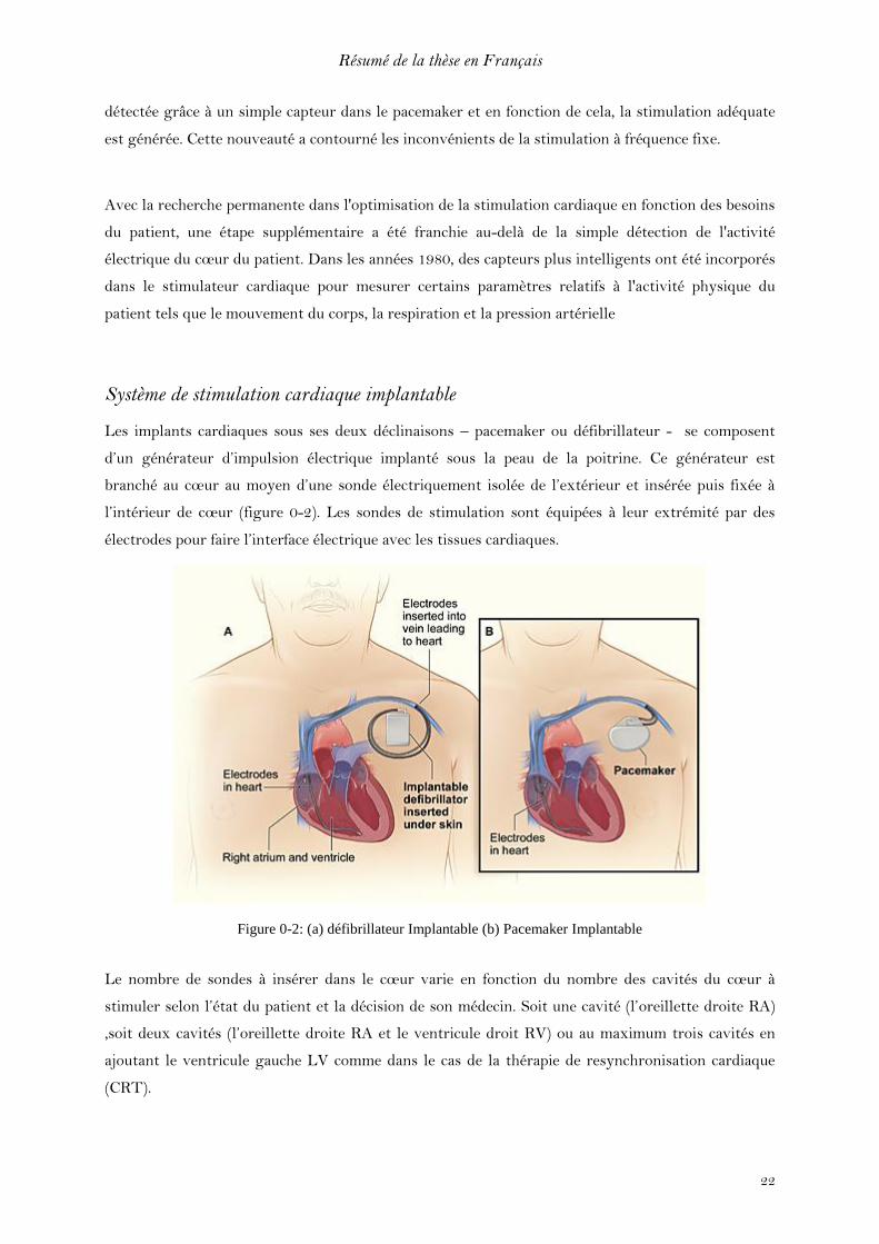
Thérapie de resynchronisation cardiaque (CRT)
La contraction ventriculaire non synchronisée est l'un des principaux symptômes de l'insuffisance
cardiaque. Les dispositifs de CRT traitent ce problème par la stimulation de deux ventricules RV et
LV simultanément afin de resynchroniser leurs contractions.
Comme illustré dans la figure 0.3, les sondes de l’oreillette droite RA et le ventricule droit RV sont
insérées et fixées à l’intérieur de ces cavités. Contrairement au cas du ventricule gauche, où la sonde
doit être fixée à l’extérieur de la cavité. La sonde est insérée à travers une des veines ventriculaires au
voisinage de la paroi externe du ventricule gauche (paroi libre). Une fois la paroi libre du ventricule
gauche atteinte, une position stable de la sonde doit être obtenue avec la meilleure réponse cardiaque
à la stimulation.
Figure 0-3: CRT pacemaker avec trios sondes de stimulation connectés au cœur
En plus de cette procédure compliquée, une stimulation ventriculaire gauche connaît un certain
nombre de difficultés telles que:
La stimulation du nerf phrénique souvent provoquée par la stimulation du ventricule gauche
qui génère des effets indésirables chez le patient comme le hoquet et les crampes
abdominales. Un moyen d'éviter cela est de placer la sonde dans une autre veine. Si cela n'est
pas possible, certaines études ont montré que cela peut être évité en changeant la distance
inter-électrode dans la sonde
Le choix limité du site de stimulation pour le médecin face à la diminution de diamètre de la
veine qui l'oblige à fixer le conducteur à un certain point et choisir le meilleur site de
Résumé de la thèse en Français
24
stimulation disponible. L'emploi d'un nombre limité d'électrodes à l'intérieur de la sonde
bipolaire limite encore davantage ce choix dans les veines du ventricule gauche
le déplacement de la sonde qui peut causer une inhibition de la réponse cardiaque à la
stimulation. Dans ce cas, une autre intervention chirurgicale semblable à la première est
nécessaire afin de repositionner la sonde ventriculaire gauche.
Ce type de complications est inévitable à cause des sondes bipolaires ordinaires qui ne proposent pas
une solution non-invasive. Pour cela nous présenterons dans le prochain chapitre le processus de
conception d'un système multi-électrodes de stimulation qui pallie les limites de la stimulation
ventriculaire gauche.
Résumé de la thèse en Français
25
Chapitre 3: Système Multi-Electrodes Pour La Stimulation
Ventriculaire Gauche: Conception et Mise en Œuvre
Ce chapitre présente un système multi-électrodes pour faire face aux limitations de la stimulation du
ventricule gauche. Dans ce chapitre, nous allons montrer comment le système multi-électrodes offre
aux médecins une plus grande souplesse dans le choix du meilleur site de stimulation pour leurs
patients, ce qui permet une meilleure gestion de la stimulation du nerf phrénique. En outre, nous
verrons aussi que le système de multi-électrodes réduit considérablement la probabilité des
interventions chirurgicales qui est nécessaire pour repositionner la sonde en cas de déplacement de
cette dernière. Ainsi, la sonde multi-électrodes permet un meilleur traitement et une meilleure
gestion des maladies cardiaques.
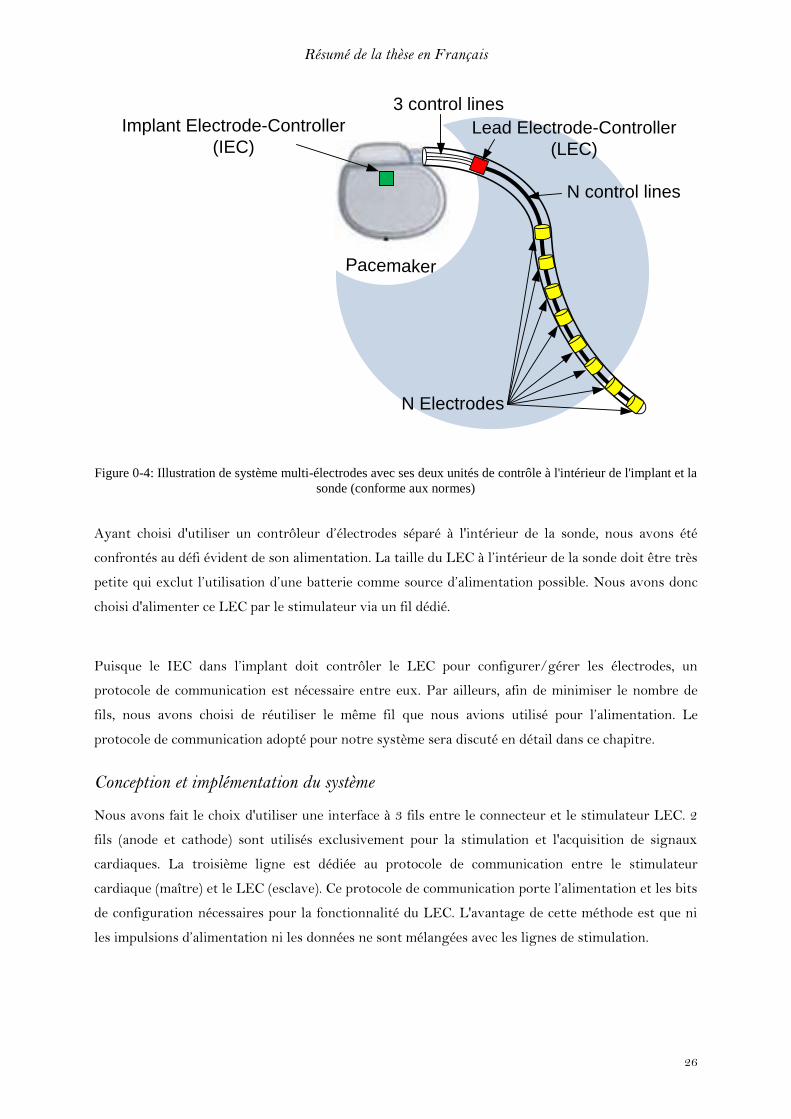
Système Multi-Electrode : Principe & Contraintes
La figure 0-4 montre le système multi-électrodes et ses composants. Similaire aux systèmes
classiques de stimulation cardiaque, le système multi-électrodes est composé d'un implant
(pacemaker), une sonde multi-électrodes et des électrodes. En raison de la multiplicité des électrodes
destinées à être activés sélectivement, un contrôleur d’électrode est nécessaire pour définir l'activité
et la polarité de chaque électrode individuellement dans la sonde.
Comme tout système, notre système multi-électrodes avait ses contraintes qui nous ont poussé de
trouver des solutions de contournement en phase de conception. La première contrainte était
comment contrôler l’ensemble des électrodes (plus que 3 électrodes) dans la sonde tout en respectant
les normes qui limitent le nombre de fils qui traversent le connecteur de l’implant à 2 ou 3 fils. Nous
avons fait un choix de conception de distribuer le contrôleur des électrodes sur deux parties. La
première réside dans l’implant même (Implant Electrode Controller - IEC), et la deuxième est
transférée de l’implant à la sonde (Lead Electrode Controller - LEC) comme c’est illustré dans la
figure 0-4. De cette façon le nombre de fils qui traversent le connecteur est de 2 ou 3 (conforme à la
norme) et chaque électrode a son fil de contrôle. IEC et LEC communiquent mutuellement via 2 à 3
fils de contrôle.
Résumé de la thèse en Français
26
PacemakerPacemaker
Lead Electrode-Controller
(LEC)
N Electrodes
3 control lines
Implant Electrode-Controller
(IEC)
N control lines
Figure 0-4: Illustration de système multi-électrodes avec ses deux unités de contrôle à l'intérieur de l'implant et la
sonde (conforme aux normes)
Ayant choisi d'utiliser un contrôleur d’électrodes séparé à l'intérieur de la sonde, nous avons été
confrontés au défi évident de son alimentation. La taille du LEC à l’intérieur de la sonde doit être très
petite qui exclut l’utilisation d’une batterie comme source d’alimentation possible. Nous avons donc
choisi d'alimenter ce LEC par le stimulateur via un fil dédié.
Puisque le IEC dans l’implant doit contrôler le LEC pour configurer/gérer les électrodes, un
protocole de communication est nécessaire entre eux. Par ailleurs, afin de minimiser le nombre de
fils, nous avons choisi de réutiliser le même fil que nous avions utilisé pour l’alimentation. Le
protocole de communication adopté pour notre système sera discuté en détail dans ce chapitre.
Conception et implémentation du système
Nous avons fait le choix d'utiliser une interface à 3 fils entre le connecteur et le stimulateur LEC. 2
fils (anode et cathode) sont utilisés exclusivement pour la stimulation et l'acquisition de signaux
cardiaques. La troisième ligne est dédiée au protocole de communication entre le stimulateur
cardiaque (maître) et le LEC (esclave). Ce protocole de communication porte l’alimentation et les bits
de configuration nécessaires pour la fonctionnalité du LEC. L'avantage de cette méthode est que ni
les impulsions d’alimentation ni les données ne sont mélangées avec les lignes de stimulation.
Résumé de la thèse en Français
27
Par ailleurs, nous nous sommes engagés à assurer la compatibilité de notre sonde multi-électrodes
avec tous les stimulateurs du marché. Nous l’avons pris en compte en mettant en place une unité de
commutation auxiliaire dans le LEC dont le rôle est de garder un lien actif entre le stimulateur
cardiaque et le cœur du patient par au moins deux électrodes sans aucune consommation d'énergie.
Cette unité auxiliaire permet également d’obtenir une faible consommation d'énergie pour l'ensemble
du système.
Nous avons également inclue une fonction supplémentaire appelée stimulation double. Elle permet
d’appliquer deux impulsions de stimulation consécutives. La première et la deuxième stimulation
peuvent être soient appliquées sur la même configuration d’électrodes ou sur deux configurations
différentes. Cette fonction ouvre une voie de recherche clinique qui peut démontrer son utilité dans
l'amélioration de la stimulation cardiaque.
Une unité de contrôle à l'intérieur d'un implant classique (pacemaker) gère la séquence d'actions et
d’événements au sein du cycle de stimulation. Ce cycle de stimulation se compose de trois phases: la
détection, la stimulation et la décharge
Lors de la phase de détection, la chaine de détection d’un pacemaker filtre et analyse les
signaux cardiaques acquis pour détecter des troubles de l'activité cardiaque du patient.
En cas de trouble cardiaque détecté, une demande de stimulation est générée qui déclenche le
circuit de sortie pour démarrer la phase de stimulation et de fournir une impulsion électrique
au cœur sur les électrodes configurées.
Ensuite la phase de décharge élimine les charges résiduelles provenant de l'interface
électrode-tissu et le chemin de la stimulation/détection.
Dans notre système multi-électrodes, une phase supplémentaire a été insérée entre la demande de
stimulation et sa livraison. Cette phase de préparation a pour mission de fournir à la LEC dans la
sonde l’alimentation nécessaire et les bits de configuration des électrodes.
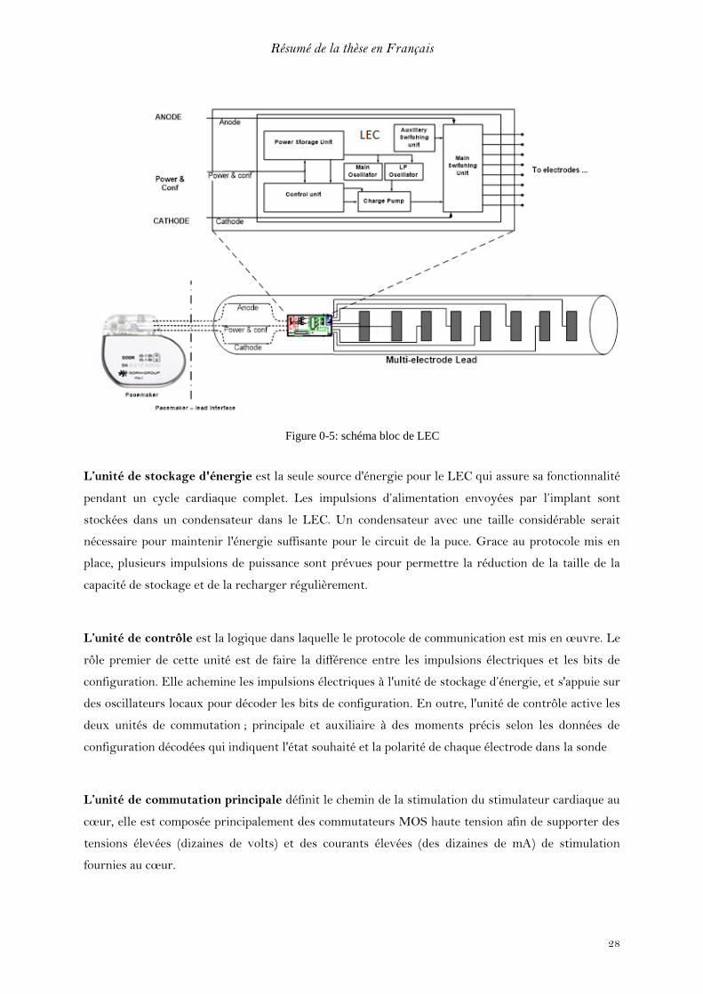
Nous avons conçu la LEC, sous la forme d'un ASIC (Application-Specific Integrated Circuit) pour
être inséré à l'intérieur de la sonde, comme illustré dans la figure 0-5 où nous présentons les blocs
principaux de la puce LEC.
Résumé de la thèse en Français
28
Figure 0-5: schéma bloc de LEC
L’unité de stockage d'énergie est la seule source d'énergie pour le LEC qui assure sa fonctionnalité
pendant un cycle cardiaque complet. Les impulsions d’alimentation envoyées par l’implant sont
stockées dans un condensateur dans le LEC. Un condensateur avec une taille considérable serait
nécessaire pour maintenir l'énergie suffisante pour le circuit de la puce. Grace au protocole mis en
place, plusieurs impulsions de puissance sont prévues pour permettre la réduction de la taille de la
capacité de stockage et de la recharger régulièrement.
L’unité de contrôle est la logique dans laquelle le protocole de communication est mis en œuvre. Le
rôle premier de cette unité est de faire la différence entre les impulsions électriques et les bits de
configuration. Elle achemine les impulsions électriques à l'unité de stockage d’énergie, et s'appuie sur
des oscillateurs locaux pour décoder les bits de configuration. En outre, l'unité de contrôle active les
deux unités de commutation ; principale et auxiliaire à des moments précis selon les données de
configuration décodées qui indiquent l'état souhaité et la polarité de chaque électrode dans la sonde
L’unité de commutation principale définit le chemin de la stimulation du stimulateur cardiaque au
cœur, elle est composée principalement des commutateurs MOS haute tension afin de supporter des
tensions élevées (dizaines de volts) et des courants élevées (des dizaines de mA) de stimulation
fournies au cœur.
Résumé de la thèse en Français
29
Le chemin entre le stimulateur et les électrodes configurées doit être maintenu en gardant les
commutateurs MOS configurés actif. L'unité de contrôle maintient cette stimulation pendant les
phases de décharge. Pendant la phase de détection, l'unité de commutation auxiliaire prend en charge
ce rôle pour transmettre les signaux cardiaques au stimulateur.
L’unité de commutation auxiliaire est activée dans le LEC lorsque le niveau d’alimentation
diminue. Cette unité est capable de maintenir la connexion entre les électrodes et le stimulateur
cardiaque, sans aucune alimentation électrique. Dans une première mise en œuvre, nous avons utilisé
des interrupteurs JFET. Ils sont normalement actifs, tandis que pour les déconnecter une
alimentation est nécessaire pour forcer l'état inactif. C'est le cas pendant la phase de détection. Il est
difficile d'estimer une durée fixe pour cette phase, afin de dimensionner le condensateur de stockage.
Un autre avantage de l'utilisation d'une telle unité de commutation auxiliaire est d'assurer une
compatibilité avec n'importe quel stimulateur du marché. Le fait que cette unité est connectée sans
source d'énergie, elle assure une connexion minimale dans la sonde multi-électrodes afin d'agir
comme une sonde bipolaire simple. Cette connexion est indépendante de tout protocole de
communication spécifique qui peut exister dans n'importe quel système multi-électrodes. C'est un
atout supplémentaire pour notre système par rapport aux autres solutions multi-électrodes.
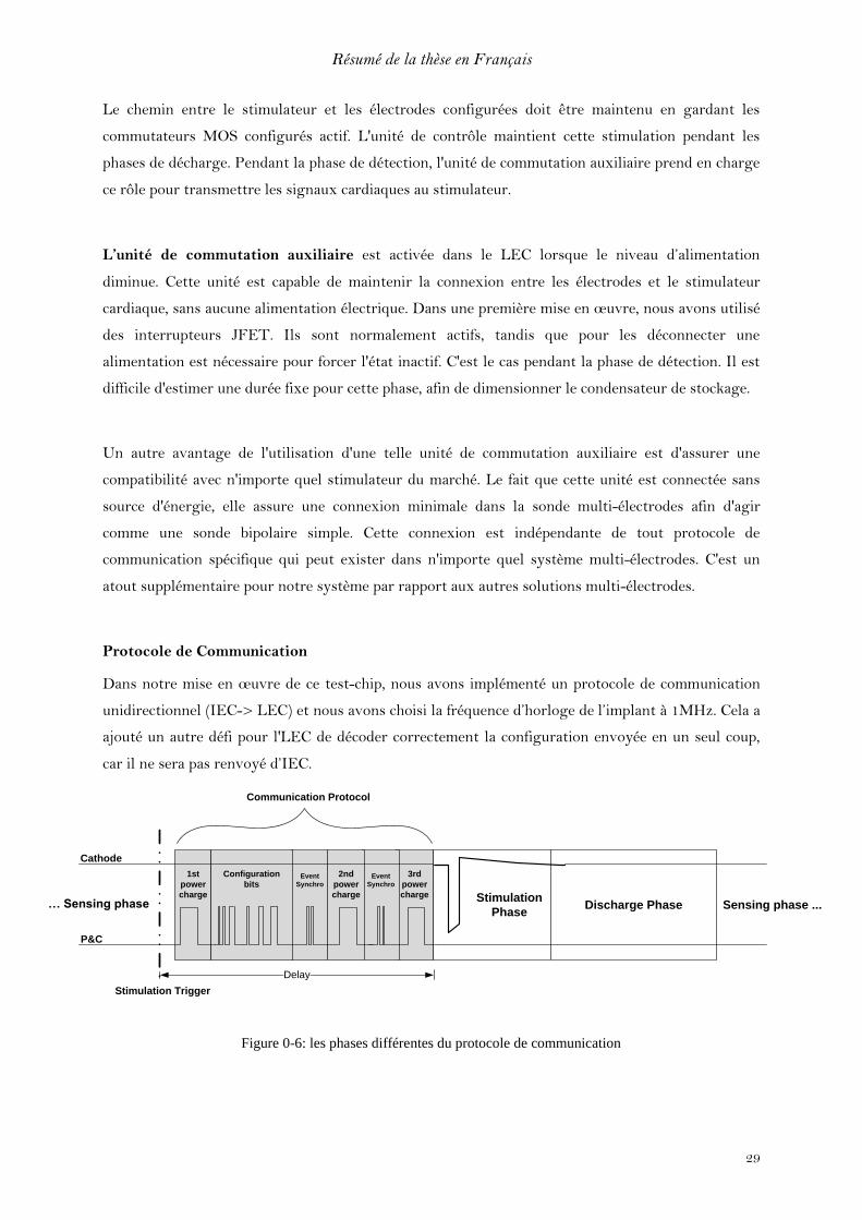
Protocole de Communication
Dans notre mise en œuvre de ce test-chip, nous avons implémenté un protocole de communication
unidirectionnel (IEC-> LEC) et nous avons choisi la fréquence d’horloge de l’implant à 1MHz. Cela a
ajouté un autre défi pour l'LEC de décoder correctement la configuration envoyée en un seul coup,
car il ne sera pas renvoyé d’IEC.
3rd
power
charge
Event
Synchro
Event
Synchro
1st
power
charge
Configuration
bits
2nd
power
charge
Discharge Phase
P&C
Cathode
… Sensing phase
Stimulation Trigger
Sensing phase ...
Communication Protocol
Delay
Stimulation
Phase
Figure 0-6: les phases différentes du protocole de communication
Résumé de la thèse en Français
30
Impulsions d’Alimentation:
Les phases de recharge ont été placées avant chaque activité consommant de l'énergie prévue pour
les circuits de LEC. En plus du réveil (Wake-Up) du LEC, cette première phase assure qu'il y a
suffisamment d’énergie pour la phase de configuration. La dernière phase d'alimentation est placée
juste avant la phase de stimulation pour faire en sorte que l'unité de commutation a une énergie
suffisante pour maintenir l'état des électrodes configurées lors de la phase de stimulation et la phase
de décharge qui intervient juste après.
Bits de synchronisation d'événements
Ils sont insérés avant les actions à effectuées par le LEC à un moment précis. En outre, ces bits de
synchronisation d'événement aident l'unité de contrôle du LEC à différencier entre les bits de
communication et les impulsions d’alimentation
Bits de configuration
Ils transportent les informations de l'activité et de la polarité de chaque électrode dans la sonde
multi-électrodes. Cette information est nommée ici "bits de données". D'autres types de bits tels que
"calibration" et "sync" complètent la structure des bits de configuration.
Le décodage de données est basé sur le comptage des cycles d'horloge par bit pour l'acquisition de sa
valeur à son milieu. En raison du déphasage entre l’oscillateur du LEC et celui du stimulateur
cardiaque qui pourrait à tort estimer le nombre de bits côté LEC, nous mettons en place trois
mécanismes:
o Calibration: ce mécanisme évalue le nombre de cycles d'horloge qui composent un bit
en fonction de l’oscillateur du LEC.
o Synchronisation des données: dans une trame, un bit de synchronisation est ajouté
après chaque 4 bits de données. Cela nous aide à éviter la propagation des erreurs
dans la trame. Cette approche est similaire à la communication de données
asynchrones « start-stop » utilisées dans la synchronisation de caractère en ASCII.
o Synchronisation de trame : chaque trame est décalée dans le temps de façon à être
synchronisé avec l'horloge LEC. Cela garantit que le décodeur compte correctement
la longueur de chaque bit uniquement sur la base de cycles d'horloge complets. (En
nombre de cycles d'horloge).
Résumé de la thèse en Français
31
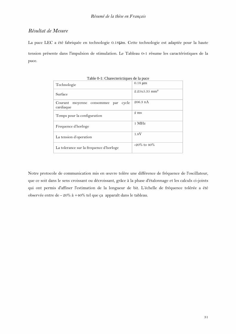
Résultat de Mesure
La puce LEC a été fabriquée en technologie 0.18μm. Cette technologie est adaptée pour la haute
tension présente dans l'impulsion de stimulation. Le Tableau 0-1 résume les caractéristiques de la
puce.
Table 0-1: Charecterictiques de la puce
Technologie 0.18 µm
Surface 2.25x5.35 mm²
Courant moyenne consommee par cycle cardiaque
206.3 nA
Temps pour la configuration 2 ms
Frequence d’horloge 1 MHz
La tension d’operation 1.8V
La tolerance sur la frequence d’horloge -20% to 40%
Notre protocole de communication mis en œuvre tolère une différence de fréquence de l'oscillateur,
que ce soit dans le sens croissant ou décroissant, grâce à la phase d'étalonnage et les calculs ci-joints
qui ont permis d'affiner l'estimation de la longueur de bit. L’échelle de fréquence tolérée a été
observée entre de - 20% à +40% tel que ça apparaît dans le tableau.
Résumé de la thèse en Français
32
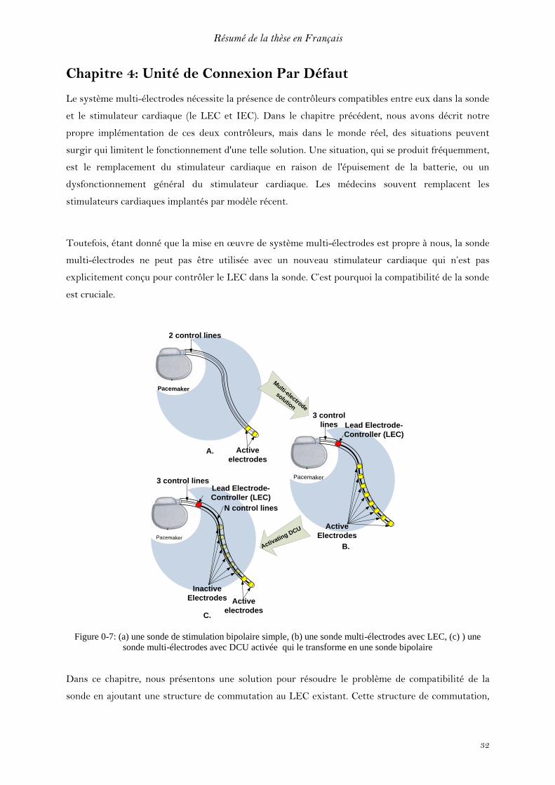
Chapitre 4: Unité de Connexion Par Défaut
Le système multi-électrodes nécessite la présence de contrôleurs compatibles entre eux dans la sonde
et le stimulateur cardiaque (le LEC et IEC). Dans le chapitre précédent, nous avons décrit notre
propre implémentation de ces deux contrôleurs, mais dans le monde réel, des situations peuvent
surgir qui limitent le fonctionnement d'une telle solution. Une situation, qui se produit fréquemment,
est le remplacement du stimulateur cardiaque en raison de l'épuisement de la batterie, ou un
dysfonctionnement général du stimulateur cardiaque. Les médecins souvent remplacent les
stimulateurs cardiaques implantés par modèle récent.
Toutefois, étant donné que la mise en œuvre de système multi-électrodes est propre à nous, la sonde
multi-électrodes ne peut pas être utilisée avec un nouveau stimulateur cardiaque qui n’est pas
explicitement conçu pour contrôler le LEC dans la sonde. C’est pourquoi la compatibilité de la sonde
est cruciale.
Pacemaker
PacemakerPacemaker
Pacemaker
Lead Electrode-
Controller (LEC)
N control lines
Active
Electrodes
Lead Electrode-
Controller (LEC)
3 control
lines
3 control lines
Active
electrodes
Inactive
Electrodes
2 control lines
Active
electrodes
Multi-electrode
solution
Activatin
g DCU
A.
B.
C.
Figure 0-7: (a) une sonde de stimulation bipolaire simple, (b) une sonde multi-électrodes avec LEC, (c) ) une
sonde multi-électrodes avec DCU activée qui le transforme en une sonde bipolaire
Dans ce chapitre, nous présentons une solution pour résoudre le problème de compatibilité de la
sonde en ajoutant une structure de commutation au LEC existant. Cette structure de commutation,
Résumé de la thèse en Français
33
appelée DCU (Unité de connexion par défaut), permet à la sonde multi-électrodes de fonctionner
comme une sonde bipolaire standard (fig. 0-7c) sans avoir besoin de configuration supplémentaire ou
d'alimentation. Le DCU est conçu pour être autonome et indépendant de tout protocole de
communication entre un stimulateur cardiaque et son contrôleur dans la sonde.
Notre structure DCU peut être adaptée à n'importe quel procédé technologique, car elle est basée sur
des transistors MOS ordinaires et présente donc une solution versatile. Les solutions existantes
étaient basées sur des composants discrets et donc n'étaient pas viables en raison de contraintes de
taille de la puce LEC.
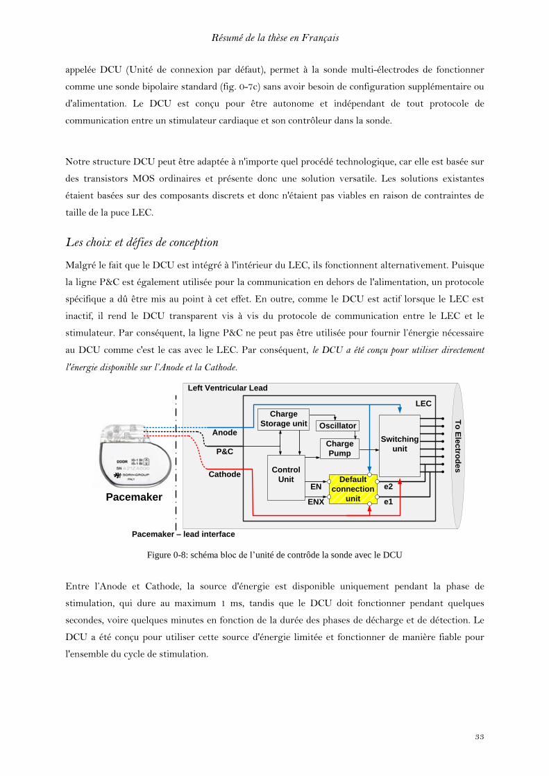
Les choix et défies de conception
Malgré le fait que le DCU est intégré à l'intérieur du LEC, ils fonctionnent alternativement. Puisque
la ligne P&C est également utilisée pour la communication en dehors de l'alimentation, un protocole
spécifique a dû être mis au point à cet effet. En outre, comme le DCU est actif lorsque le LEC est
inactif, il rend le DCU transparent vis à vis du protocole de communication entre le LEC et le
stimulateur. Par conséquent, la ligne P&C ne peut pas être utilisée pour fournir l’énergie nécessaire
au DCU comme c'est le cas avec le LEC. Par conséquent, le DCU a été conçu pour utiliser directement
l'énergie disponible sur l’Anode et la Cathode.
Pacemaker
Pacemaker – lead interface
Left Ventricular Lead
To
Ele
ctro
de
s
EN
ENX
Switching
unit
Default
connection
unit
Anode
P&C
Cathode
Charge
Storage unit
Control
Unit
Oscillator
Charge
Pump
LEC
e1
e2
Figure 0-8: schéma bloc de l’unité de contrôde la sonde avec le DCU
Entre l’Anode et Cathode, la source d'énergie est disponible uniquement pendant la phase de
stimulation, qui dure au maximum 1 ms, tandis que le DCU doit fonctionner pendant quelques
secondes, voire quelques minutes en fonction de la durée des phases de décharge et de détection. Le
DCU a été conçu pour utiliser cette source d'énergie limitée et fonctionner de manière fiable pour
l'ensemble du cycle de stimulation.
Résumé de la thèse en Français
34
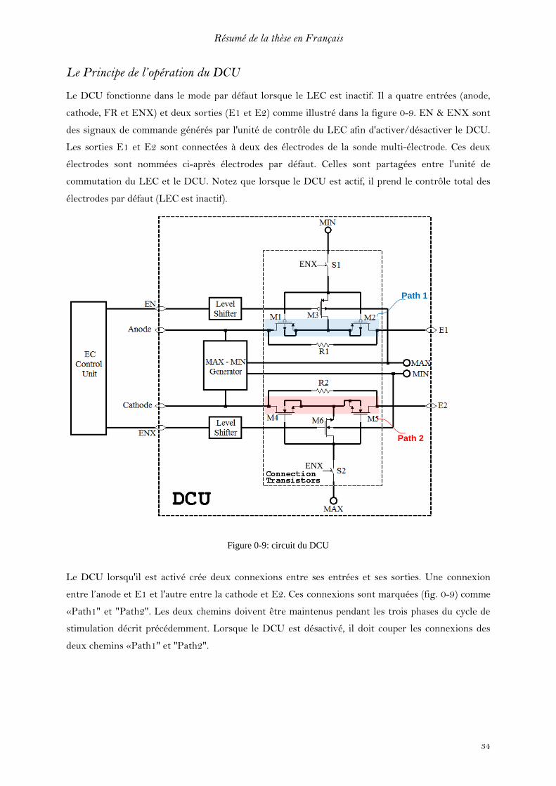
Le Principe de l’opération du DCU
Le DCU fonctionne dans le mode par défaut lorsque le LEC est inactif. Il a quatre entrées (anode,
cathode, FR et ENX) et deux sorties (E1 et E2) comme illustré dans la figure 0-9. EN & ENX sont
des signaux de commande générés par l'unité de contrôle du LEC afin d'activer/désactiver le DCU.
Les sorties E1 et E2 sont connectées à deux des électrodes de la sonde multi-électrode. Ces deux
électrodes sont nommées ci-après électrodes par défaut. Celles sont partagées entre l'unité de
commutation du LEC et le DCU. Notez que lorsque le DCU est actif, il prend le contrôle total des
électrodes par défaut (LEC est inactif).
Path 1
Path 2
ENX
ENX
Figure 0-9: circuit du DCU
Le DCU lorsqu'il est activé crée deux connexions entre ses entrées et ses sorties. Une connexion
entre l’anode et E1 et l'autre entre la cathode et E2. Ces connexions sont marquées (fig. 0-9) comme
«Path1" et "Path2". Les deux chemins doivent être maintenus pendant les trois phases du cycle de
stimulation décrit précédemment. Lorsque le DCU est désactivé, il doit couper les connexions des
deux chemins «Path1" et "Path2".
Résumé de la thèse en Français
35
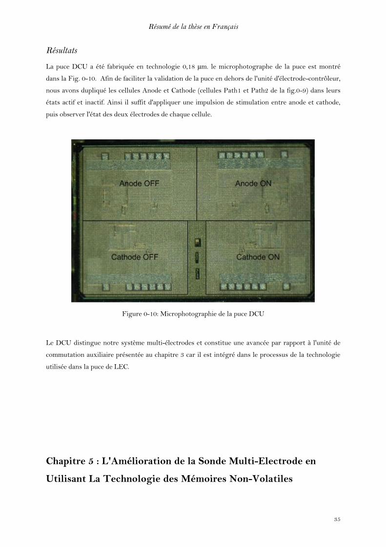
Résultats
La puce DCU a été fabriquée en technologie 0,18 µm. le microphotographe de la puce est montré
dans la Fig. 0-10. Afin de faciliter la validation de la puce en dehors de l'unité d'électrode-contrôleur,
nous avons dupliqué les cellules Anode et Cathode (cellules Path1 et Path2 de la fig.0-9) dans leurs
états actif et inactif. Ainsi il suffit d'appliquer une impulsion de stimulation entre anode et cathode,
puis observer l'état des deux électrodes de chaque cellule.
Figure 0-10: Microphotographie de la puce DCU
Le DCU distingue notre système multi-électrodes et constitue une avancée par rapport à l'unité de
commutation auxiliaire présentée au chapitre 3 car il est intégré dans le processus de la technologie
utilisée dans la puce de LEC.
Chapitre 5 : L'Amélioration de la Sonde Multi-Electrode en
Utilisant La Technologie des Mémoires Non-Volatiles
Résumé de la thèse en Français
36
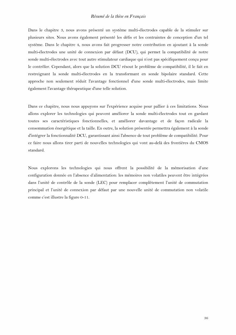
Dans le chapitre 3, nous avons présenté un système multi-électrodes capable de la stimuler sur
plusieurs sites. Nous avons également présenté les défis et les contraintes de conception d'un tel
système. Dans le chapitre 4, nous avons fait progresser notre contribution en ajoutant à la sonde
multi-électrodes une unité de connexion par défaut (DCU), qui permet la compatibilité de notre
sonde multi-électrodes avec tout autre stimulateur cardiaque qui n’est pas spécifiquement conçu pour
le contrôler. Cependant, alors que la solution DCU résout le problème de compatibilité, il le fait en
restreignant la sonde multi-électrodes en la transformant en sonde bipolaire standard. Cette
approche non seulement réduit l'avantage fonctionnel d'une sonde multi-électrodes, mais limite
également l'avantage thérapeutique d'une telle solution.
Dans ce chapitre, nous nous appuyons sur l'expérience acquise pour pallier à ces limitations. Nous
allons explorer les technologies qui peuvent améliorer la sonde multi-électrodes tout en gardant
toutes ses caractéristiques fonctionnelles, et améliorer davantage et de façon radicale la
consommation énergétique et la taille. En outre, la solution présentée permettra également à la sonde
d'intégrer la fonctionnalité DCU, garantissant ainsi l'absence de tout problème de compatibilité. Pour
ce faire nous allons tirer parti de nouvelles technologies qui vont au-delà des frontières du CMOS
standard.
Nous explorons les technologies qui nous offrent la possibilité de la mémorisation d’une
configuration donnée en l’absence d’alimentation: les mémoires non volatiles peuvent être intégrées
dans l’unité de contrôle de la sonde (LEC) pour remplacer complètement l’unité de commutation
principal et l’unité de connexion par défaut par une nouvelle unité de commutation non volatile
comme c’est illustre la figure 0-11.
Résumé de la thèse en Français
37
Pacemaker
Pacemaker – lead interface
Left Ventricular Lead
To
Ele
ctro
de
s
EN
ENX
Main
Switching
unit
Default
connection
unit
Anode
P&C
Cathode
Charge
Storage unit
Control
Unit
Oscillator
Charge
Pump
EC
e1
e2
Pacemaker
Pacemaker – lead interface
Left Ventricular Lead
To
Ele
ctro
de
s
Non-Volatile
Switching
unit
Anode
P&C
Cathode
Charge
Storage unit
Control
Unit
Oscillator
Charge
Pump
EC
Figure 0-11: Remplacement de l'unité de commutation principal et l'unité de connexion par défaut par la
nouvelle unité de commutation non-volatile à l'intérieur de l’unité de contrôle de la sonde (LEC)
Notez que conserver le dernier état configuré du système multi-électrodes nous permettra d'éviter la
répétition de la reprogrammation du système. Cela permettrait non seulement une réduction de la
consommation en énergie (un objectif clé de la conception), mais aussi d’éliminer la latence (due à la
programmation) et en plus le remplacement du stimulateur ne conduirait pas à des problèmes
d'incompatibilité. Ainsi, la mémorisation d'état nous conduirait à une solution gagnant-gagnant, où
nous adressons tous nos défis de conception et de compatibilité.
Dans les sections 5.3 et 5.4 nous avons détaillé l’état de l’art des technologies non volatiles et nous
avons présenté des résultats de simulation ainsi que l’étude de faisabilité en vue de son intégration au
sein de notre système. Voici le résumé de toutes ces directions:
Nous avons vu à quel point une technologie électromécanique à base de nanotubes de
carbone comme les NRAM peut être prometteuse pour notre application. Ses états stables de
commutation, la très grande variation des résistances à l’état passant et bloqué; sa vitesse et
sa petite taille en font d’elle la candidate idéale pour notre application.
STT MTJ et Memristance ont été regroupées sous la famille RAM résistive pour leurs
caractéristiques communes du point de vue applicatif. Après nos investigations, nous sommes
parvenus à la conclusion que leur intégration dans notre système n'est pas faisable en raison
de leur instabilité face à des tensions et des courants importants de stimulation.
Résumé de la thèse en Français
38
Finalement, nous avons étudié les cellules de mémoire flash et nous avons proposé une
nouvelle structure où les cellules flash sont associées à des transistors MOS pour faire des
commutateurs non volatils. Dans cette structure la tension et le courant de stimulation
passent à travers les transistors MOS, tandis que les cellules flash sont utilisées pour définir
et conserver l'état du transistor MOS.
Nous avons breveté le concept de l’intégration des technologies de mémoire non volatile dans les
implants cardiaques.
Résumé de la thèse en Français
39
Fin du Résumé

General Introduction
40
1 Chapter 1
General Introduction

General Introduction
41
General Introduction
[1] Kadish A, Mehra M. Heart failure devices: implantable cardioverter-defibrillators and biventricular pacing therapy. Circulation 2005 http://circ.ahajournals.org/content/111/24/3327.full [2] Zipes DP, Wellens HJ. Sudden cardiac death. Circulation. 1998; 98: 2334–2351. [3] Myerburg RJ, Interian AJ, Mitrani RM, Kessler KM, Castellanos A. Frequency of sudden cardiac death and profiles of risk. Am J Cardiol. 1997; 80: 10F–19F. [4] S. A.P. Haddad, R.P.M. Houben and W. A. Serdijn “The Evolution of Pacemakers” IEEE EMB Magazine, Vol. 25, No. 3, May/June 2006, pp38 – 48.
42
In the recent years the standards of health care delivery have improved by leaps and bounds.
Thanks to path-breaking research, new discoveries, new materials and advancements in technology,
human beings not only live longer lives, but are administered better therapy which reduces the
chances of disease progression and enables early detection of maladies. However it is important to
note, that despite these advancements there is scope and need for much improvement especially in
dreaded medical conditions such as cardiovascular complication which affect a large section of our
population.
In various studies it is estimated that cardiovascular diseases are the principal cause of death
especially in advanced industrial societies [1] [2]. In United States alone cardiovascular diseases are
reported to be the number one cause of death [3]. Worldwide it is estimated that around 40% of all
human deaths are due to cardiac complications [4].
In this thesis we will look at cardiac implants used to manage cardiovascular therapy, particularly
pacemakers and defibrillators. We will look at the basic construction of these devices from an
electronics perspective and we will also discuss their evolution. Furthermore, we will present our
research results which we believe will enhance these devices by improving their functionality and
making them more efficient. The chapter wise plan of this thesis is as follows:
In chapter2 we present basic functioning of heart, the prominent cardiovascular diseases and the
devices used to manage these diseases i.e. cardiac implants. We discuss in detail, evolution of cardiac
implants and their basic components. Thereafter we discuss in detail one of the most prevalent
cardiac malady i.e. heart failure. Furthermore, we discuss bi-ventricular stimulation which is the
mechanism used to manage heart failure.
In chapter3 we present the multi-electrode system to address the problem of biventricular
stimulation. We present the design challenges the design philosophy and the constraints of such a
multi-electrode system. We also discuss in detail the existing solutions and their limitations. Finally,
we present the performance and results of the system which was designed by us.

Cardiac Stimulation Implants
43
In chapter4 we present the design of an additional block of the multi-electrode system we
presented in chapter 3. The addition of this block to our multi-electrode lead solves the problem of
compatibility of our multi-electrode system with existing pacemakers. As in chapter 3 we present in
detail the design philosophy, constraints and the performance/results of our system
In chapter5 we look at new technologies beyond the standard CMOS, which can make our multi-
electrode lead smarter, smaller and more performant. We present several candidate technologies
which can be applied in our multi-electrode. We discuss their strengths, weakness and their merits
and demerits. Finally through simulations we prove the feasibility of some of these technologies for
our application.
The main contributions of the thesis are as follows:
Design and implementation of a multi electrode system: We designed and implemented a
multi-electrode system which is capable of multi-site and multiple stimulation. Our solution is
completely configurable and meets the drastic constraints of area and power imposed by nature of
our application. Our chip was taped out in .18 µm technology and occupies 2.25x5.35 mm² area. The
chip also features a specially designed communication protocol and is compliant with the existing
standards. It enables low power operation and allows quick configuration. To the best of our
knowledge our study is the first published study of its kind.
Design and implementation of default connection unit: We implemented a default connection
unit block for the multi-electrode chip which enabled the operation of a multi electrode lead with
pacemakers not designed specifically to control such a lead. The solution therefore enlarges our lead
compatibility to cover all pacemakers in the market. In the chapter we also discuss and provide
solutions to the key challenges of such design in a constrained cardiac environment. Like the multi-
electrode block the DCU block was taped out in 0.18 µm technology, occupies 2.2 x 1.75 mm² area
and harvests the stimulation energy to power itself.
Proof of concept of the non-volatile memory technologies in the multi-electrode system:
New technologies were explored which drastically improve the performance of the multi-electrode
system. The employment of such technologies enhanced our multi-electrode system by eliminating
the need of repetitive configuration of electrodes, thereby saving power and reducing latency. The
benefits also included smaller area and compatibility with any pacemaker in the market. We explored
several nonvolatile technologies, like NRAM, MRAM, Memristance and Flash. Through simulations
we proved the feasibility of these technologies for our implant applications. We believe such
technologies will be leveraged to design the next generation ultra-low power and ultra-high
performance leads.
Cardiac Stimulation Implants
44
2 Chapter 2
Cardiac Stimulation Implants

Cardiac Stimulation Implants
45
Cardiac Stimulation Implants
46
2.1 Introduction
Cardiac stimulation implants are life saving devices of about the size of a child’s palm, implanted in
the patient’s chest to manage different disorders that may affect the heart. We will start this chapter
by presenting the basic functioning of heart, the main cardiovascular disorders and how cardiac
implants address those disorders. We will then discuss the evolution of cardiac implants and their
basic components. Thereafter we discuss in detail one of the most prevalent cardiac malady i.e. heart
failure. Furthermore, we discuss bi-ventricular stimulation which is the mechanism used to manage
heart failure.
2.2 Human Heart and Cardiac Implant Evolution
The heart is one of the most important organs in our body. It is a muscular organ which pumps
blood through the network of arteries and veins known as the cardiovascular system. As shown in
figure 2-1, the heart is composed of four chambers: two receiving chambers; Right Atrium (RA) &
Left Atrium (LA) and two pumping chambers; Right Ventricle (RV) & Left Ventricle (LV) as shown
in figure 2-1.
Figure 2-1: Heart Chambers [6]
Each minute the heart beats approximately 72 times. During this short period, RA pumps about 5
liters [5] of deoxygenated blood to the lungs while LV pumps about 5 liters of oxygenated blood to
the rest of the organs. The amount of blood pumped each minute by the left ventricle is termed
“cardiac output”. A significant decrease in this amount decreases the oxygen level in the organs
which may lead to loss of conscious or even death if the affected organ was the brain.

Cardiac Stimulation Implants
47
The heart is composed of two types of muscle cells; contractile and autorhythmic cells. Contractile
cells represent the majority (99%) and are responsible for the heart contraction which leads to the
mechanical pumping. Autorhythmic cells are less in number but play the vital role in initiation and
conduction of action potentials. Action potential is defined as the rapid change of membrane
electrical potential during excitation and then leads to transmission of electrical impulses travelling
across the membrane. This action potential initiation and conduction done by autorhythmic cells is
responsible for the rhythmic and coordinated contraction of the heart chambers.
Figure 2-2 shows the electrical conduction system of the heart which governs its rhythm of
contraction. Each heart beat is initiated by an electrical signal generated at the Sinoatrilal node (SA
node) located at the top of the right atrium. This electrical signal creates a depolarization wave that
spreads rapidly in the right and left atria (RA & LA) causing them to contract. Due to electrical
insulation between atria and ventricles, the depolarization wave does not reach the ventricles.
Instead, the electrical activity reaches the ventricles via a second node called Atrioventricular node
(AV node). This node is connected to a bundle of specialized cells called “Bundle of His” which
divides into right and left bundle branches inside right and left ventricles respectively. These
branches divides further into tiny fibers called “Purkinje fibers” to disperse rapidly the electrical
signal inside the ventricles [6].
Figure 2-2: Conduction system of the heart [5]
In this electrical conduction system, the SA node acts as the natural pacemaker which sets the
rate at which the heart beats. Any disturbance in this conduction system causes cardiac disorders
such as arrhythmias or heart failure.
Cardiac Stimulation Implants
48
2.2.1 Heart failure condition
Heart failure is a progressive condition affecting patients whose heart cannot pump enough blood
to meet the needs of their body. This condition is associated with uncoordinated ventricular
contractions and causes symptoms like breathing difficulty and lack of energy. The first method of
treatment is medication. Thereafter Cardiac Resynchronization Therapy (CRT) pacemakers are
prescribed for patients with moderate to severe heart failure. Cardiac Resynchronization Therapy
pacemakers do not have the ability to treat abnormal fast rhythm (VT and VF) with rapid pacing or
a defibrillation shock.
2.2.2 Arrhythmias
Arrhythmia is defined as an abnormal heart rhythm which can be too fast or too slow, or
irregular. Arrhythmias can be a life-threatening condition which may lead to a cardiac arrest. Cardiac
arrest rarely gives any warnings, and once it occurs it requires an immediate intervention from a
doctor or emergency medical personnel to provide a shock (defibrillation) in order to restore normal
heart rhythm. Well, these kinds of resources are not always available in proximity of the patient. For
patients whom medication was not sufficient to address the cause of such arrhythmias, Implantable
cardioverter defibrillator (ICD) can offer a protection against such life-threatening condition.
Nowadays an implantable cardioverter defibrillator ICD with a cardiac rhythm therapy CRT is
available and offers the required treatment for heart failure condition and protection against life-
threatening situations.
The cardiac implant is generally implanted just under the chest skin and it delivers the electrical
stimulation via specialized wires (called leads) to the chambers of heart. To deliver the electrical
stimulation to the tissue the lead is equipped at its end with electrodes. Generally in the simplest
embodiment, the number of electrodes is either two (bipolar) or one (unipolar).
2.2.3 First Implantable pacemaker
In 1959, the engineer Wilson Greatbatch developed the first fully implantable pacemaker [7]. It
delivered electrical pulses of fixed width and amplitude at fixed rate of 60 beats per minute (bpm). It
was powered by ten mercury-zinc cells battery that gave it an estimated lifetime of five years.
The limitation of this asynchronous (fixed rate) pacemaker was the delivery of stimulation pulses
at fixed rate regardless of the cardiac activity. This activity competes with the natural activity of the
heart leading sometimes to cardiac disorders.
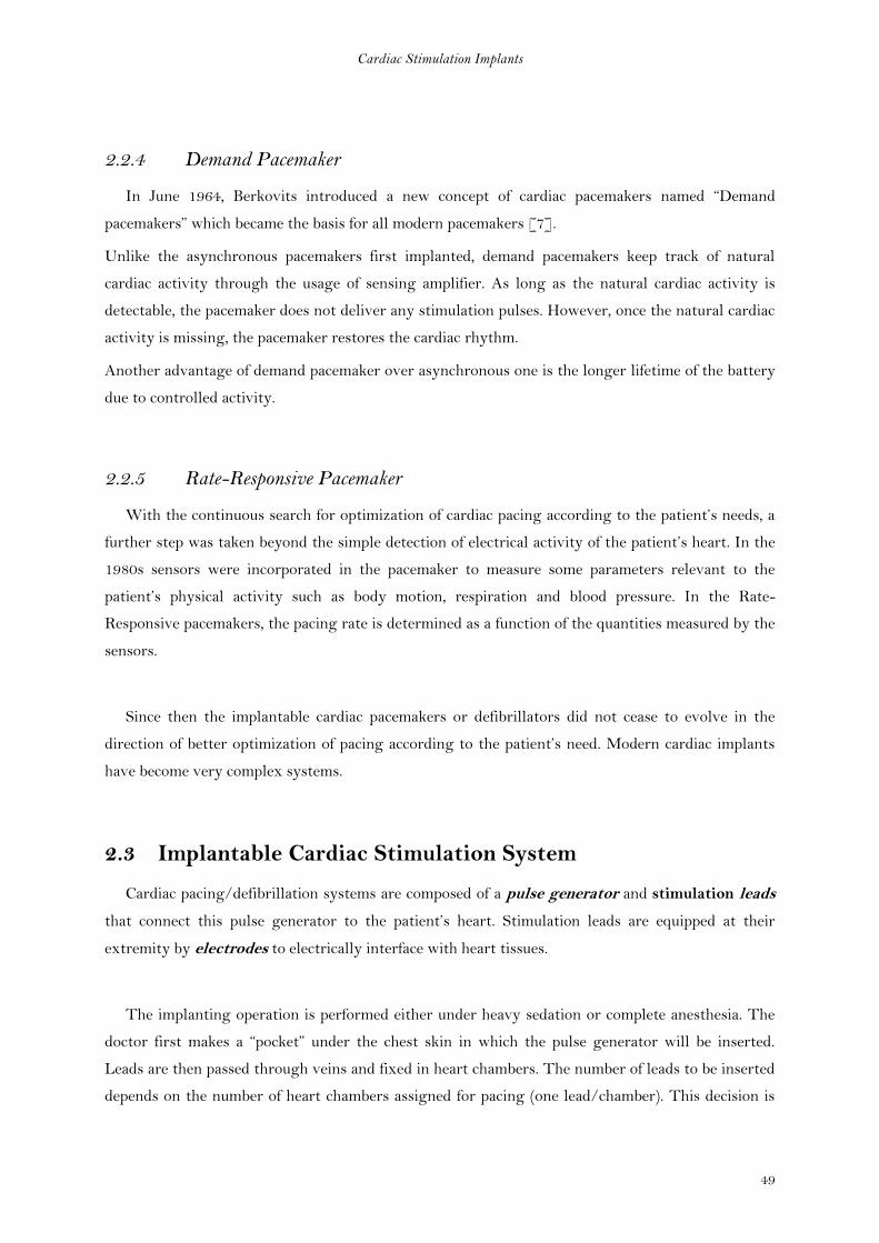
Cardiac Stimulation Implants
49
2.2.4 Demand Pacemaker
In June 1964, Berkovits introduced a new concept of cardiac pacemakers named “Demand
pacemakers” which became the basis for all modern pacemakers [7].
Unlike the asynchronous pacemakers first implanted, demand pacemakers keep track of natural
cardiac activity through the usage of sensing amplifier. As long as the natural cardiac activity is
detectable, the pacemaker does not deliver any stimulation pulses. However, once the natural cardiac
activity is missing, the pacemaker restores the cardiac rhythm.
Another advantage of demand pacemaker over asynchronous one is the longer lifetime of the battery
due to controlled activity.
2.2.5 Rate-Responsive Pacemaker
With the continuous search for optimization of cardiac pacing according to the patient’s needs, a
further step was taken beyond the simple detection of electrical activity of the patient’s heart. In the
1980s sensors were incorporated in the pacemaker to measure some parameters relevant to the
patient’s physical activity such as body motion, respiration and blood pressure. In the Rate-
Responsive pacemakers, the pacing rate is determined as a function of the quantities measured by the
sensors.
Since then the implantable cardiac pacemakers or defibrillators did not cease to evolve in the
direction of better optimization of pacing according to the patient’s need. Modern cardiac implants
have become very complex systems.
2.3 Implantable Cardiac Stimulation System
Cardiac pacing/defibrillation systems are composed of a pulse generator and stimulation leads
that connect this pulse generator to the patient’s heart. Stimulation leads are equipped at their
extremity by electrodes to electrically interface with heart tissues.
The implanting operation is performed either under heavy sedation or complete anesthesia. The
doctor first makes a “pocket” under the chest skin in which the pulse generator will be inserted.
Leads are then passed through veins and fixed in heart chambers. The number of leads to be inserted
depends on the number of heart chambers assigned for pacing (one lead/chamber). This decision is

Cardiac Stimulation Implants
50
made by the doctor depending on the patient’s needs, either one chamber pacing (RA) or double
chamber pacing (RA and RV) or maximally triple chamber pacing (RA, RV and LV).
Figure 2-3: (a) implantable defibrillator (b) Implantable pacemaker [9]
Figure 2-3 shows as example for the position of the cardiac implant whether a defibrillator (fig. 2-
3a) or pacemaker (fig. 2-3b) and the leads fixed in two heart chambers RA and RV (dual chamber
pacing mode).
After leads insertion and before their final fixation, the doctor has to test the cardiac response to
stimulation in order to determine the best site for stimulation.
Pulse generator is powered by batteries of limited lifetime estimated to last 7 or 10 years
depending on the pacing activity. Several months before the battery is expected to run out, the pulse
generator is replaced in an operation similar to the original implant. The pocket in the chest is re-
opened and the new pulse generator is connected to existing leads only if they are tested to be in
good state. Leads are occasionally replaced and their replacement can be more complex than the
replacement of pulse generator.
In the following subsections we will discuss the basic components of a pulse generator and the
leads features.
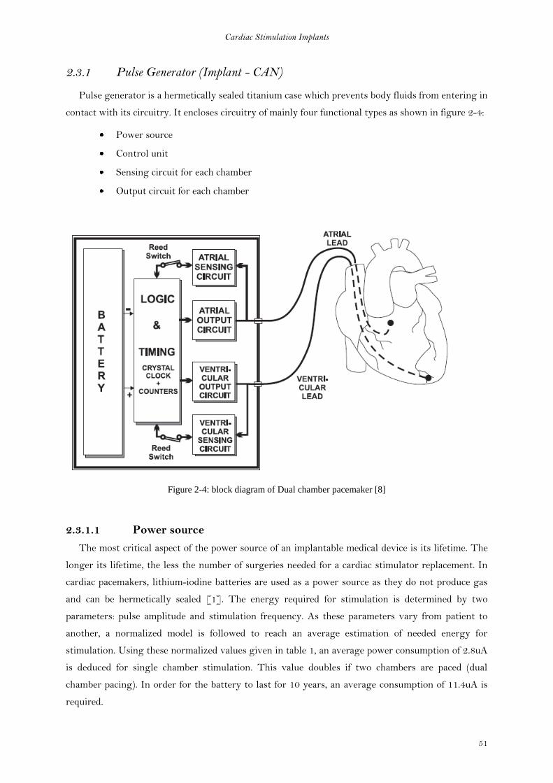
Cardiac Stimulation Implants
51
2.3.1 Pulse Generator (Implant - CAN)
Pulse generator is a hermetically sealed titanium case which prevents body fluids from entering in
contact with its circuitry. It encloses circuitry of mainly four functional types as shown in figure 2-4:
Power source
Control unit
Sensing circuit for each chamber
Output circuit for each chamber
Figure 2-4: block diagram of Dual chamber pacemaker [8]
2.3.1.1 Power source
The most critical aspect of the power source of an implantable medical device is its lifetime. The
longer its lifetime, the less the number of surgeries needed for a cardiac stimulator replacement. In
cardiac pacemakers, lithium-iodine batteries are used as a power source as they do not produce gas
and can be hermetically sealed [1]. The energy required for stimulation is determined by two
parameters: pulse amplitude and stimulation frequency. As these parameters vary from patient to
another, a normalized model is followed to reach an average estimation of needed energy for
stimulation. Using these normalized values given in table 1, an average power consumption of 2.8uA
is deduced for single chamber stimulation. This value doubles if two chambers are paced (dual
chamber pacing). In order for the battery to last for 10 years, an average consumption of 11.4uA is
required.
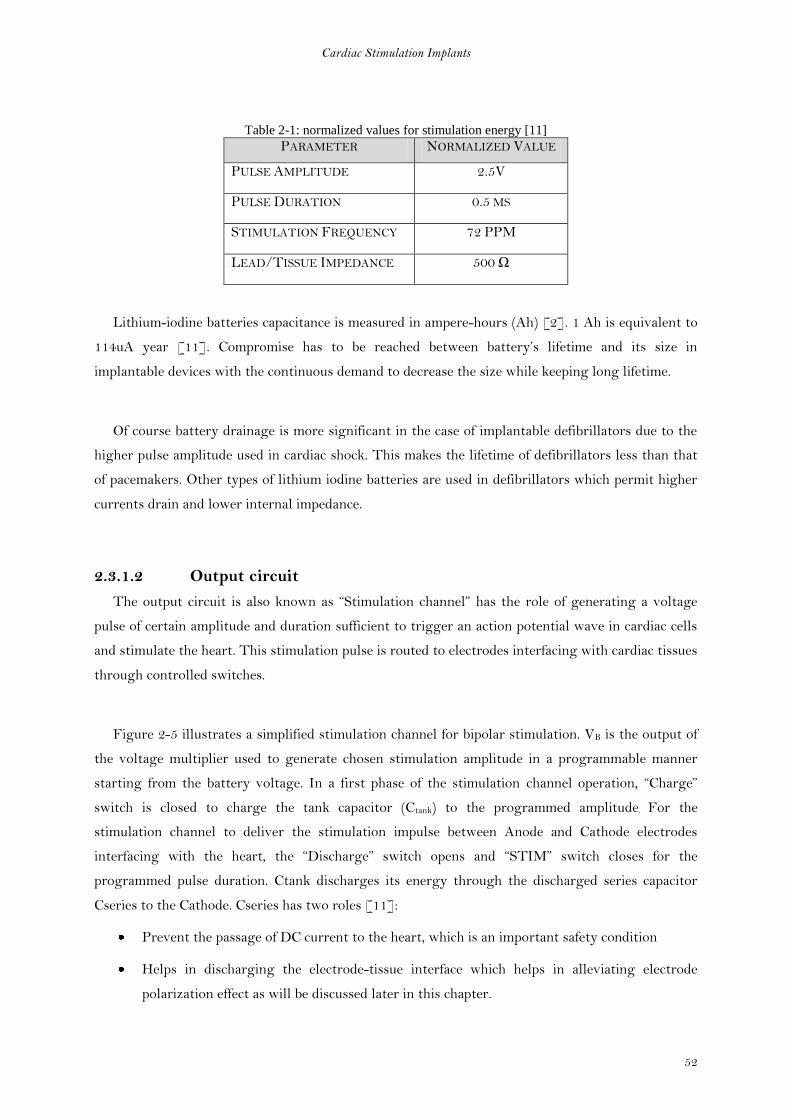
Cardiac Stimulation Implants
52
Table 2-1: normalized values for stimulation energy [11]
PARAMETER NORMALIZED VALUE
PULSE AMPLITUDE 2.5V
PULSE DURATION 0.5 MS
STIMULATION FREQUENCY 72 PPM
LEAD/TISSUE IMPEDANCE 500 Ω
Lithium-iodine batteries capacitance is measured in ampere-hours (Ah) [2]. 1 Ah is equivalent to
114uA year [11]. Compromise has to be reached between battery’s lifetime and its size in
implantable devices with the continuous demand to decrease the size while keeping long lifetime.
Of course battery drainage is more significant in the case of implantable defibrillators due to the
higher pulse amplitude used in cardiac shock. This makes the lifetime of defibrillators less than that
of pacemakers. Other types of lithium iodine batteries are used in defibrillators which permit higher
currents drain and lower internal impedance.
2.3.1.2 Output circuit
The output circuit is also known as “Stimulation channel” has the role of generating a voltage
pulse of certain amplitude and duration sufficient to trigger an action potential wave in cardiac cells
and stimulate the heart. This stimulation pulse is routed to electrodes interfacing with cardiac tissues
through controlled switches.
Figure 2-5 illustrates a simplified stimulation channel for bipolar stimulation. VB is the output of
the voltage multiplier used to generate chosen stimulation amplitude in a programmable manner
starting from the battery voltage. In a first phase of the stimulation channel operation, “Charge”
switch is closed to charge the tank capacitor (Ctank) to the programmed amplitude. For the
stimulation channel to deliver the stimulation impulse between Anode and Cathode electrodes
interfacing with the heart, the “Discharge” switch opens and “STIM” switch closes for the
programmed pulse duration. Ctank discharges its energy through the discharged series capacitor
Cseries to the Cathode. Cseries has two roles [11]:
Prevent the passage of DC current to the heart, which is an important safety condition
Helps in discharging the electrode-tissue interface which helps in alleviating electrode
polarization effect as will be discussed later in this chapter.
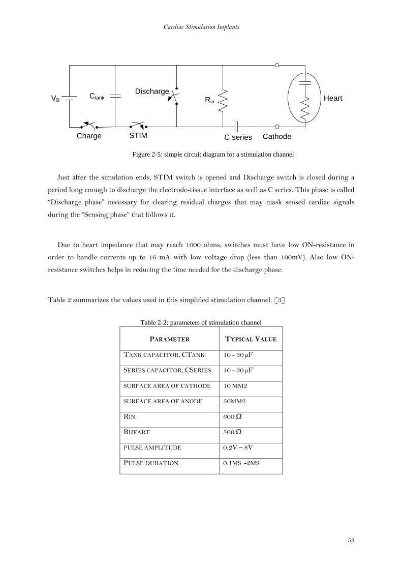
Cardiac Stimulation Implants
53
STIM
Ctank
C series
DischargeRin
CathodeCharge
HeartVB
Figure 2-5: simple circuit diagram for a stimulation channel
Just after the simulation ends, STIM switch is opened and Discharge switch is closed during a
period long enough to discharge the electrode-tissue interface as well as C series. This phase is called
“Discharge phase” necessary for clearing residual charges that may mask sensed cardiac signals
during the “Sensing phase” that follows it.
Due to heart impedance that may reach 1000 ohms, switches must have low ON-resistance in
order to handle currents up to 16 mA with low voltage drop (less than 100mV). Also low ON-
resistance switches helps in reducing the time needed for the discharge phase.
Table 2 summarizes the values used in this simplified stimulation channel. [3]
Table 2-2: parameters of stimulation channel
PARAMETER TYPICAL VALUE
TANK CAPACITOR, CTANK 10 - 30 µF
SERIES CAPACITOR, CSERIES 10 - 30 µF
SURFACE AREA OF CATHODE 10 MM2
SURFACE AREA OF ANODE 50MM2
RIN 600 Ω
RHEART 500 Ω
PULSE AMPLITUDE 0.2V – 8V
PULSE DURATION 0.1MS -2MS
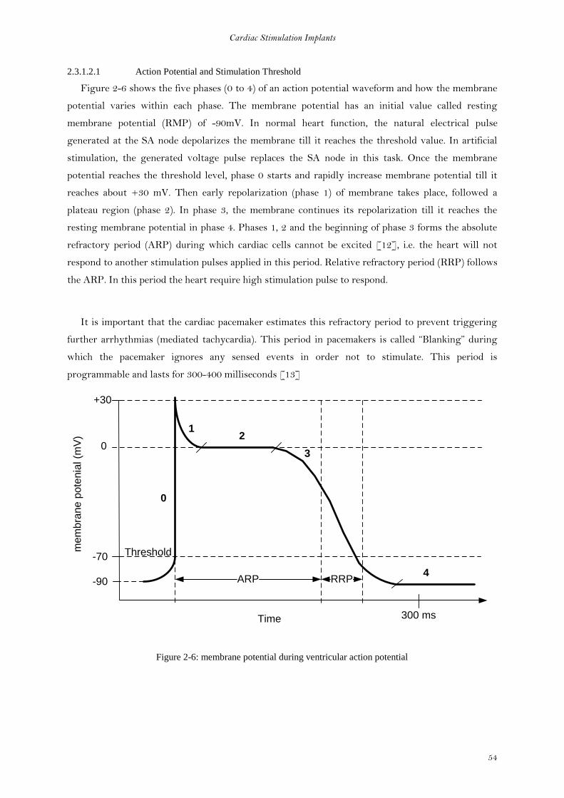
Cardiac Stimulation Implants
54
2.3.1.2.1 Action Potential and Stimulation Threshold
Figure 2-6 shows the five phases (0 to 4) of an action potential waveform and how the membrane
potential varies within each phase. The membrane potential has an initial value called resting
membrane potential (RMP) of -90mV. In normal heart function, the natural electrical pulse
generated at the SA node depolarizes the membrane till it reaches the threshold value. In artificial
stimulation, the generated voltage pulse replaces the SA node in this task. Once the membrane
potential reaches the threshold level, phase 0 starts and rapidly increase membrane potential till it
reaches about +30 mV. Then early repolarization (phase 1) of membrane takes place, followed a
plateau region (phase 2). In phase 3, the membrane continues its repolarization till it reaches the
resting membrane potential in phase 4. Phases 1, 2 and the beginning of phase 3 forms the absolute
refractory period (ARP) during which cardiac cells cannot be excited [12], i.e. the heart will not
respond to another stimulation pulses applied in this period. Relative refractory period (RRP) follows
the ARP. In this period the heart require high stimulation pulse to respond.
It is important that the cardiac pacemaker estimates this refractory period to prevent triggering
further arrhythmias (mediated tachycardia). This period in pacemakers is called “Blanking” during
which the pacemaker ignores any sensed events in order not to stimulate. This period is
programmable and lasts for 300-400 milliseconds [13]
ARP RRP
12
3
4
300 ms
0
-90
-70
0
+30
me
mb
ran
e p
ote
nia
l (m
V)
Time
Threshold
Figure 2-6: membrane potential during ventricular action potential
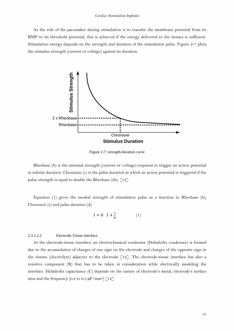
Cardiac Stimulation Implants
55
As the role of the pacemaker during stimulation is to transfer the membrane potential from its
RMP to its threshold potential, this is achieved if the energy delivered to the tissues is sufficient.
Stimulation energy depends on the strength and duration of the stimulation pulse. Figure 2-7 plots
the stimulus strength (current or voltage) against its duration.
Rheobase
2 x Rheobase
Chronaxie
Stimulus Duration
Sti
mu
lus
Str
en
gth
Figure 2-7: strength-duration curve
Rheobase (b) is the minimal strength (current or voltage) required to trigger an action potential
at infinite duration. Chronaxie (c) is the pulse duration at which an action potential is triggered if the
pulse strength is equal to double the Rheobase (2b). [12]
Equation (1) gives the needed strength of stimulation pulse as a function in Rheobase (b),
Chronaxie (c) and pulse duration (d).
(1)
2.3.1.2.2 Electrode-Tissue interface
At the electrode-tissue interface, an electrochemical condenser (Helmholtz condenser) is formed
due to the accumulation of charges of one sign on the electrode and charges of the opposite sign in
the tissues (electrolyte) adjacent to the electrode [12]. The electrode-tissue interface has also a
resistive component (R) that has to be taken in consideration while electrically modeling the
interface. Helmholtz capacitance (C) depends on the nature of electrode’s metal, electrode’s surface
area and the frequency (0.2 to 0.5 µF/mm2) [14]
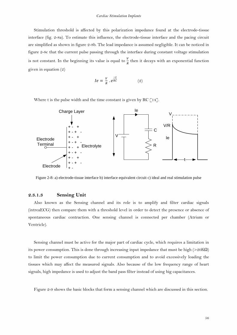
Cardiac Stimulation Implants
56
Stimulation threshold is affected by this polarization impedance found at the electrode-tissue
interface (fig. 2-8a). To estimate this influence, the electrode-tissue interface and the pacing circuit
are simplified as shown in figure 2-8b. The lead impedance is assumed negligible. It can be noticed in
figure 2-8c that the current pulse passing through the interface during constant voltage stimulation
is not constant. In the beginning its value is equal to then it decays with an exponential function
given in equation (2)
(2)
Where t is the pulse width and the time constant is given by RC [14].
t
V/R
Ie
Ie
V
R
C
V
+ - +
+ - + -
+ - +
+ - + -
+ - +
+ - + -
+ - +
+ - + -
+ -
Electrolyte
Charge Layer
Electrode
Terminal
Electrode
Figure 2-8: a) electrode-tissue interface b) interface equivalent circuit c) ideal and real stimulation pulse
2.3.1.3 Sensing Unit
Also known as the Sensing channel and its role is to amplify and filter cardiac signals
(intreaECG) then compare them with a threshold level in order to detect the presence or absence of
spontaneous cardiac contraction. One sensing channel is connected per chamber (Atrium or
Ventricle).
Sensing channel must be active for the major part of cardiac cycle, which requires a limitation in
its power consumption. This is done through increasing input impedance that must be high (>20KΩ)
to limit the power consumption due to current consumption and to avoid excessively loading the
tissues which may affect the measured signals. Also because of the low frequency range of heart
signals, high impedance is used to adjust the band pass filter instead of using big capacitances.
Figure 2-9 shows the basic blocks that form a sensing channel which are discussed in this section.
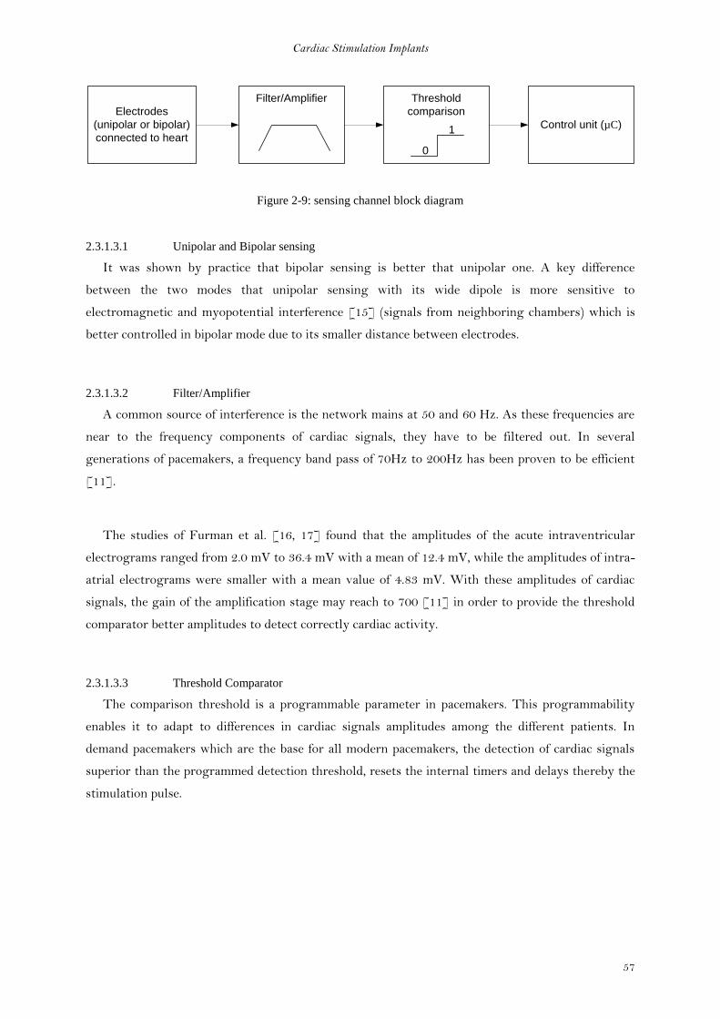
Cardiac Stimulation Implants
57
Electrodes
(unipolar or bipolar)
connected to heart
Filter/Amplifier Threshold
comparison
Control unit (µC)
0
1
Figure 2-9: sensing channel block diagram
2.3.1.3.1 Unipolar and Bipolar sensing
It was shown by practice that bipolar sensing is better that unipolar one. A key difference
between the two modes that unipolar sensing with its wide dipole is more sensitive to
electromagnetic and myopotential interference [15] (signals from neighboring chambers) which is
better controlled in bipolar mode due to its smaller distance between electrodes.
2.3.1.3.2 Filter/Amplifier
A common source of interference is the network mains at 50 and 60 Hz. As these frequencies are
near to the frequency components of cardiac signals, they have to be filtered out. In several
generations of pacemakers, a frequency band pass of 70Hz to 200Hz has been proven to be efficient
[11].
The studies of Furman et al. [16, 17] found that the amplitudes of the acute intraventricular
electrograms ranged from 2.0 mV to 36.4 mV with a mean of 12.4 mV, while the amplitudes of intra-
atrial electrograms were smaller with a mean value of 4.83 mV. With these amplitudes of cardiac
signals, the gain of the amplification stage may reach to 700 [11] in order to provide the threshold
comparator better amplitudes to detect correctly cardiac activity.
2.3.1.3.3 Threshold Comparator
The comparison threshold is a programmable parameter in pacemakers. This programmability
enables it to adapt to differences in cardiac signals amplitudes among the different patients. In
demand pacemakers which are the base for all modern pacemakers, the detection of cardiac signals
superior than the programmed detection threshold, resets the internal timers and delays thereby the
stimulation pulse.
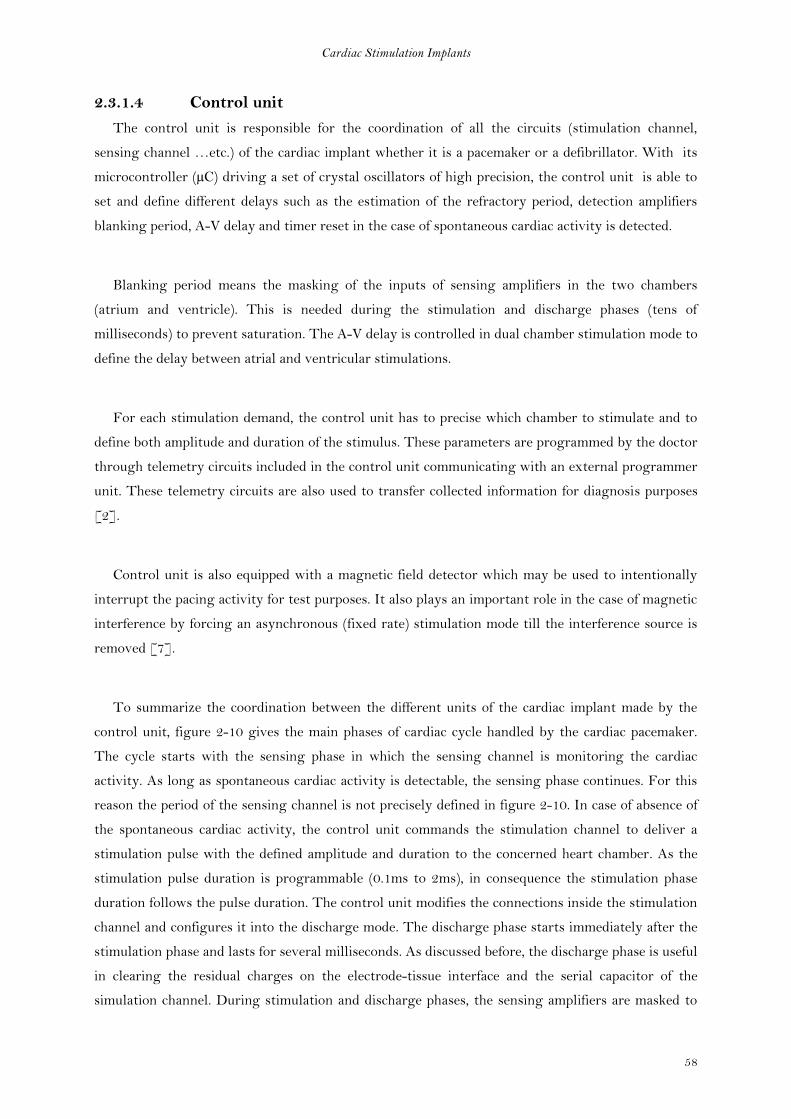
Cardiac Stimulation Implants
58
2.3.1.4 Control unit
The control unit is responsible for the coordination of all the circuits (stimulation channel,
sensing channel …etc.) of the cardiac implant whether it is a pacemaker or a defibrillator. With its
microcontroller (µC) driving a set of crystal oscillators of high precision, the control unit is able to
set and define different delays such as the estimation of the refractory period, detection amplifiers
blanking period, A-V delay and timer reset in the case of spontaneous cardiac activity is detected.
Blanking period means the masking of the inputs of sensing amplifiers in the two chambers
(atrium and ventricle). This is needed during the stimulation and discharge phases (tens of
milliseconds) to prevent saturation. The A-V delay is controlled in dual chamber stimulation mode to
define the delay between atrial and ventricular stimulations.
For each stimulation demand, the control unit has to precise which chamber to stimulate and to
define both amplitude and duration of the stimulus. These parameters are programmed by the doctor
through telemetry circuits included in the control unit communicating with an external programmer
unit. These telemetry circuits are also used to transfer collected information for diagnosis purposes
[2].
Control unit is also equipped with a magnetic field detector which may be used to intentionally
interrupt the pacing activity for test purposes. It also plays an important role in the case of magnetic
interference by forcing an asynchronous (fixed rate) stimulation mode till the interference source is
removed [7].
To summarize the coordination between the different units of the cardiac implant made by the
control unit, figure 2-10 gives the main phases of cardiac cycle handled by the cardiac pacemaker.
The cycle starts with the sensing phase in which the sensing channel is monitoring the cardiac
activity. As long as spontaneous cardiac activity is detectable, the sensing phase continues. For this
reason the period of the sensing channel is not precisely defined in figure 2-10. In case of absence of
the spontaneous cardiac activity, the control unit commands the stimulation channel to deliver a
stimulation pulse with the defined amplitude and duration to the concerned heart chamber. As the
stimulation pulse duration is programmable (0.1ms to 2ms), in consequence the stimulation phase
duration follows the pulse duration. The control unit modifies the connections inside the stimulation
channel and configures it into the discharge mode. The discharge phase starts immediately after the
stimulation phase and lasts for several milliseconds. As discussed before, the discharge phase is useful
in clearing the residual charges on the electrode-tissue interface and the serial capacitor of the
simulation channel. During stimulation and discharge phases, the sensing amplifiers are masked to
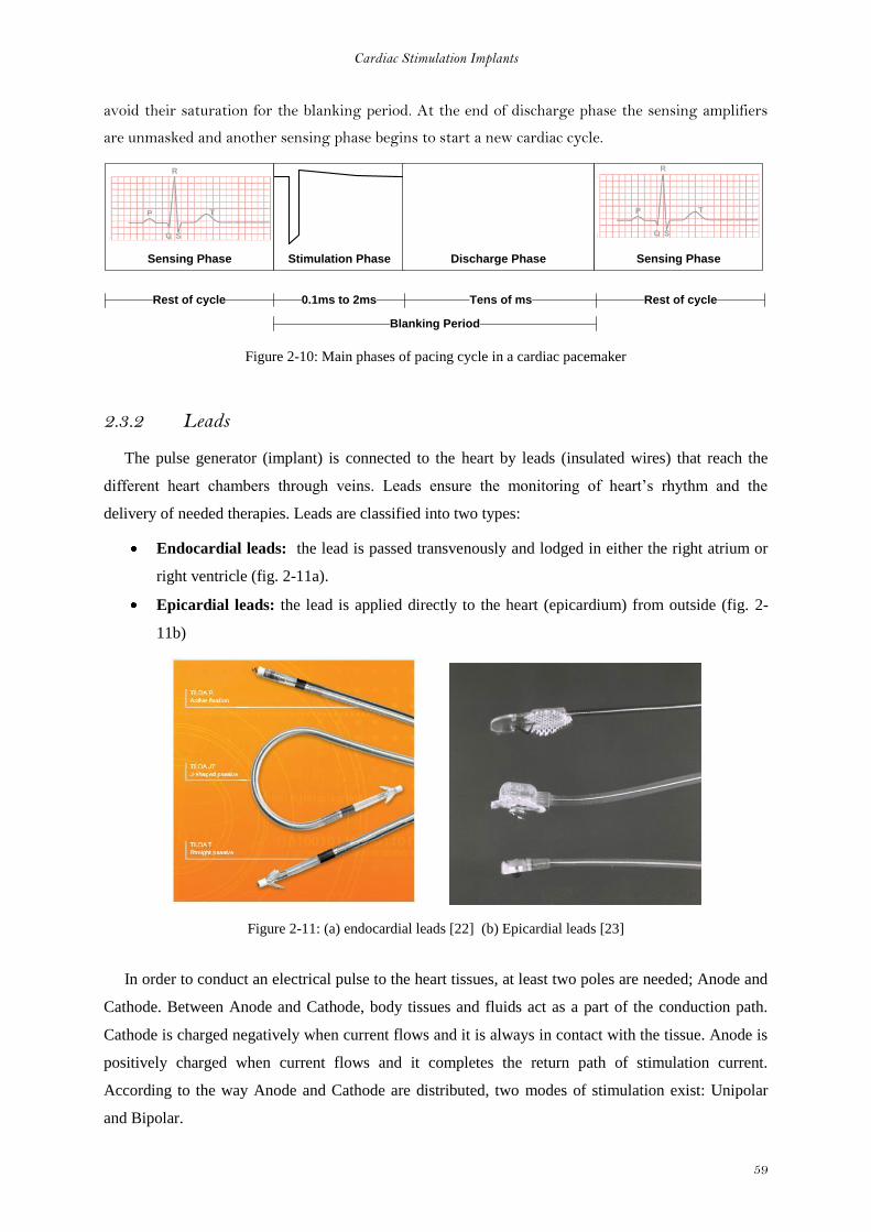
Cardiac Stimulation Implants
59
avoid their saturation for the blanking period. At the end of discharge phase the sensing amplifiers
are unmasked and another sensing phase begins to start a new cardiac cycle.
Sensing Phase Stimulation Phase Discharge Phase
Sensing Phase
Rest of cycle 0.1ms to 2ms Tens of ms
Blanking Period
Rest of cycle
Figure 2-10: Main phases of pacing cycle in a cardiac pacemaker
2.3.2 Leads
The pulse generator (implant) is connected to the heart by leads (insulated wires) that reach the
different heart chambers through veins. Leads ensure the monitoring of heart’s rhythm and the
delivery of needed therapies. Leads are classified into two types:
Endocardial leads: the lead is passed transvenously and lodged in either the right atrium or
right ventricle (fig. 2-11a).
Epicardial leads: the lead is applied directly to the heart (epicardium) from outside (fig. 2-
11b)
Figure 2-11: (a) endocardial leads [22] (b) Epicardial leads [23]
In order to conduct an electrical pulse to the heart tissues, at least two poles are needed; Anode and
Cathode. Between Anode and Cathode, body tissues and fluids act as a part of the conduction path.
Cathode is charged negatively when current flows and it is always in contact with the tissue. Anode is
positively charged when current flows and it completes the return path of stimulation current.
According to the way Anode and Cathode are distributed, two modes of stimulation exist: Unipolar
and Bipolar.
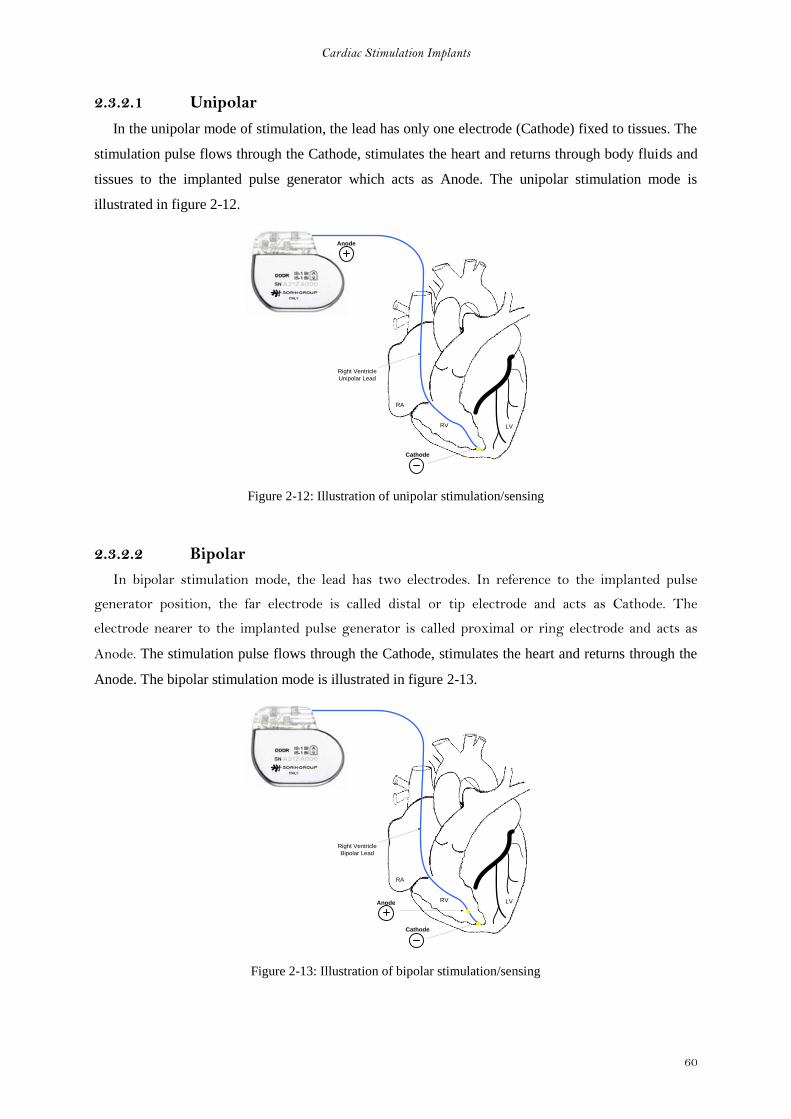
Cardiac Stimulation Implants
60
2.3.2.1 Unipolar
In the unipolar mode of stimulation, the lead has only one electrode (Cathode) fixed to tissues. The
stimulation pulse flows through the Cathode, stimulates the heart and returns through body fluids and
tissues to the implanted pulse generator which acts as Anode. The unipolar stimulation mode is
illustrated in figure 2-12.
RA
RV LV
Right Ventricle
Unipolar Lead
Cathode
Anode
Figure 2-12: Illustration of unipolar stimulation/sensing
2.3.2.2 Bipolar
In bipolar stimulation mode, the lead has two electrodes. In reference to the implanted pulse
generator position, the far electrode is called distal or tip electrode and acts as Cathode. The
electrode nearer to the implanted pulse generator is called proximal or ring electrode and acts as
Anode. The stimulation pulse flows through the Cathode, stimulates the heart and returns through the
Anode. The bipolar stimulation mode is illustrated in figure 2-13.
RA
RV LV
Right Ventricle
Bipolar Lead
Cathode
Anode
Figure 2-13: Illustration of bipolar stimulation/sensing
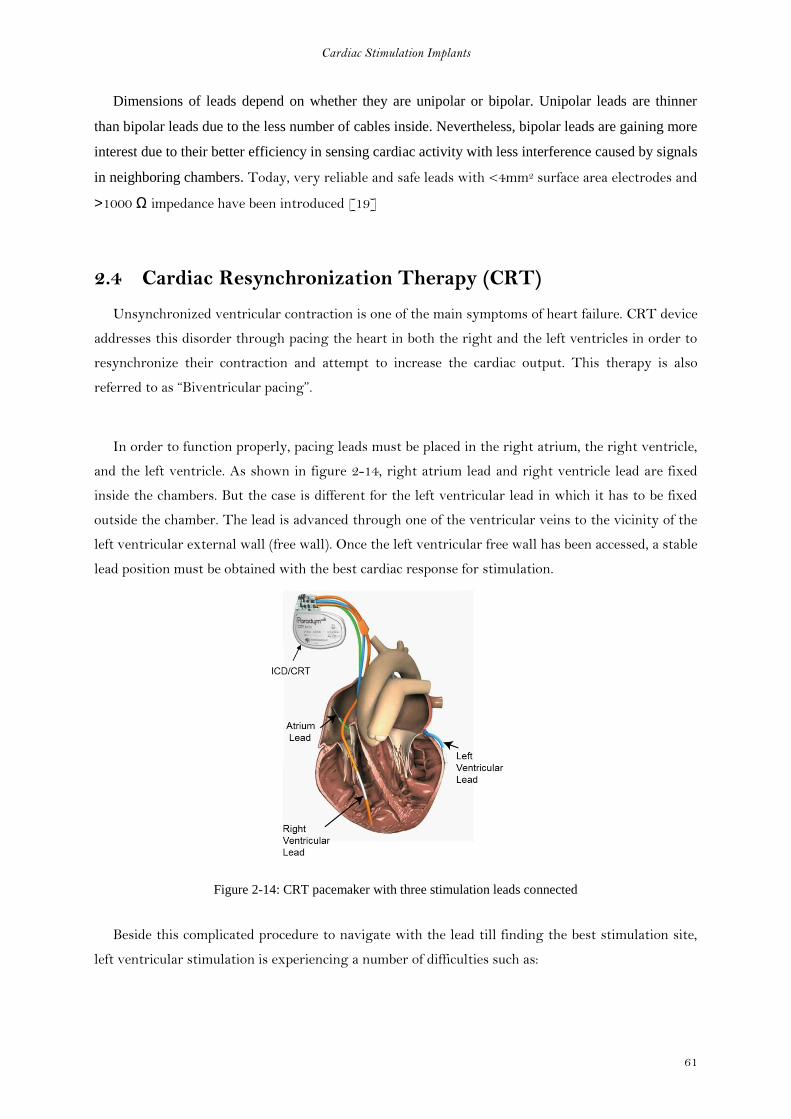
Cardiac Stimulation Implants
61
Dimensions of leads depend on whether they are unipolar or bipolar. Unipolar leads are thinner
than bipolar leads due to the less number of cables inside. Nevertheless, bipolar leads are gaining more
interest due to their better efficiency in sensing cardiac activity with less interference caused by signals
in neighboring chambers. Today, very reliable and safe leads with <4mm2 surface area electrodes and
>1000 Ω impedance have been introduced [19]
2.4 Cardiac Resynchronization Therapy (CRT)
Unsynchronized ventricular contraction is one of the main symptoms of heart failure. CRT device
addresses this disorder through pacing the heart in both the right and the left ventricles in order to
resynchronize their contraction and attempt to increase the cardiac output. This therapy is also
referred to as “Biventricular pacing”.
In order to function properly, pacing leads must be placed in the right atrium, the right ventricle,
and the left ventricle. As shown in figure 2-14, right atrium lead and right ventricle lead are fixed
inside the chambers. But the case is different for the left ventricular lead in which it has to be fixed
outside the chamber. The lead is advanced through one of the ventricular veins to the vicinity of the
left ventricular external wall (free wall). Once the left ventricular free wall has been accessed, a stable
lead position must be obtained with the best cardiac response for stimulation.
Figure 2-14: CRT pacemaker with three stimulation leads connected
Beside this complicated procedure to navigate with the lead till finding the best stimulation site,
left ventricular stimulation is experiencing a number of difficulties such as:
Cardiac Stimulation Implants
62
2.4.1 Phrenic nerve stimulation
One of the most difficult problems to troubleshoot is when after careful manipulation of a left
ventricular lead into what seems to be an ideal lateral wall location with excellent pacing thresholds,
high output stimulation results in phrenic or diaphragmatic stimulation. This erroneous stimulation
may cause hiccups and abdominal cramps [21] for the patient.
The best way to avoid phrenic nerve stimulation is to place the lead in another vein. If this is not
possible, some studies have found that this can be avoided by changing the inter-electrode distance in
the lead [20]. However with bipolar electrode leads, changing the inter-electrode distance is not
possible, the only solution is to insert a new lead which evidently increases the complexity manifold.
2.4.2 Limited choice of stimulation site
The task is already difficult for the physician facing the decreasing diameter of the vein which
obliges him to fix the lead at a certain point and choose the best stimulation site available. The
employment of limited number of electrodes inside the bipolar lead further limits the physician
choice inside the left ventricular veins.
2.4.3 Lead displacement
In some patients after a successful implantation for the left ventricular leads, an inhibition of
cardiac response to stimulation may be noticed. This may be caused due to lead displacement inside
the veins. In this case, another surgical intervention similar to the first one is needed to reposition
the left ventricular lead. This kind of complication is inevitable using the ordinary bipolar leads
which does not offer a non-invasive solution to the problem.
Cardiac Stimulation Implants
63
2.5 Conclusion
In this chapter we presented the structure of human heart as well as disorders and diseases that
may affect it. We saw how cardiac implants continued their evolution to better treat patients
suffering from cardiovascular diseases. We explored the building blocks of cardiac implants and how
they interact with cardiac tissues to analyze the patient’s state and deliver the adequate treatment.
We terminated the chapter with a presentation of the importance of biventricular pacing (CRT)
and the enumerated some limitations of bipolar leads used in left ventricular stimulation.
In the next chapter we will present the design process of a multi-electrode pacing system that
alleviates the limitations of left ventricular stimulation.
Cardiac Stimulation Implants
64
References
[1] Mond, H. G. 1983. The cardiac pacemaker, function and malfunction: 1st Ed. New York:
Grune and Stratton.
[2] John G. Webster, Design of Pacemakers, IEEE Press 1995, chapter 5
[3] John G. Webster, Design of Pacemakers, IEEE Press 1995, chapter 6
[4] WebMD.com
[5] L. Sherwood “Fundamentals of Human Physiology” Cengage Learning, 2011
[6] David Prutchi, Michael Norris “Design and development of medical electronic
instrumentation” John Wiley and Sons, 2005 - 461 pages
[7] S. A.P. Haddad, R.P.M. Houben and W. A. Serdijn “The Evolution of Pacemakers” IEEE
EMB Magazine, Vol. 25, No. 3, May/June 2006, pp38 – 48.
[8] S. S. Barold, R. X. Stroobandt, A. F. Sinnaeve “Cardiac Pacemakers step by step” Blackwell
publishing 2004.
[9] National Heart Lung Blood Institute. http://www.nhlbi.nih.gov
[10] CRT/ICD patient booklet of Sorin Group
[11] Fernando Silveira, Denis Flandre « Low power analog CMOS for cardiac pacemakers"
Springer 2004.
[12] W. A. Tacker and L. A. Geddes “The laws of electrical stimulation of cardiac tissues”
Proceedings of the IEEE, vol. 84, No. 3, March 1996
[13] G. Alec Rooke “Pacemaker Review” Professor of Anesthesiology, University of Washington,
Seattle, WA
[14] A. Ripart and J. Mugica “Electrode-Heart Interface: Definition of the Ideal Electrode” Pacing
and Clinical Electrophysiology, Wiley Volume 6, Issue 2, pages 410–421, March 1983
[15] A. P. Nielsen, W. R. Cashion, W. H. Spencer, H. J. Norton, G. W. Divine , T. D.
Schuenemeyer, J. C. Griffin “Long-Term Assessment of Unipolar and Bipolar Stimulation and
Sensing Thresholds Using a Lead Configuration Programmable Pacemaker” JACC 1985
[16] Furman, S., Hurzeler, P., and DeCaprio, V. 1977a. The ventricular endocardial electrogram
and pacemaker sensing. J. Cardiovascular and Thoracic Surg. 73: 258–266.
[17] Furman, S., Hurzeler, P., and DeCaprio, V. 1977b. Cardiac pacing and pacemakers III.
Sensing the cardiac electrogram. Am. Heart J. 93:794–801.
[18] L. A. Geddes and L. E. Baker, Principles of Applied Biomedical Instrumentation, 1st and 3rd
edition New York: Wiley, 1968, 1989.
Cardiac Stimulation Implants
65
[19] Harry G. Mond, “Recent Advances in Pacemaker Lead Technology”, Cardiac
Electrophysiology Review 1999
[20] Samuel J Asirvatham “Implanting a Left Ventricular Pacemaker Lead” Indian Heart J 2007;
59: 197–204
[21] A. K. Tadakamalla et al. “Phrenic Nerve Stimulation: An Unexpected Complication of
Implantable Cardioverter Defibrillator (ICD)” E-Journal of cardiology 2011 vol 1, N 1
[22] Sorin Group Data
[23] Medtronic, Inc. stimulation lead photo
Cardiac Stimulation Implants
66
3 Chapter 3
Multi-electrode System for Left
Ventricular Stimulation: Design and
Implementation
3. Multi-electrode System for Left Ventricular Stimulation: Design and Implementation
67
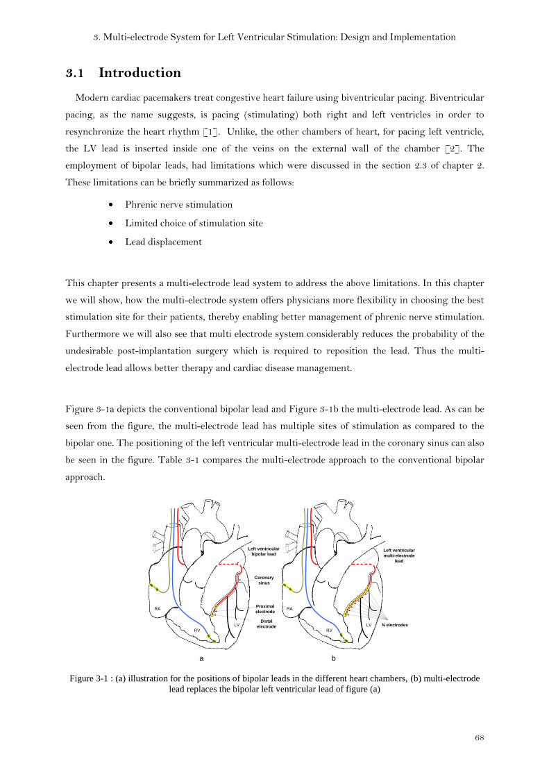
3. Multi-electrode System for Left Ventricular Stimulation: Design and Implementation
68
3.1 Introduction
Modern cardiac pacemakers treat congestive heart failure using biventricular pacing. Biventricular
pacing, as the name suggests, is pacing (stimulating) both right and left ventricles in order to
resynchronize the heart rhythm [1]. Unlike, the other chambers of heart, for pacing left ventricle,
the LV lead is inserted inside one of the veins on the external wall of the chamber [2]. The
employment of bipolar leads, had limitations which were discussed in the section 2.3 of chapter 2.
These limitations can be briefly summarized as follows:
Phrenic nerve stimulation
Limited choice of stimulation site
Lead displacement
This chapter presents a multi-electrode lead system to address the above limitations. In this chapter
we will show, how the multi-electrode system offers physicians more flexibility in choosing the best
stimulation site for their patients, thereby enabling better management of phrenic nerve stimulation.
Furthermore we will also see that multi electrode system considerably reduces the probability of the
undesirable post-implantation surgery which is required to reposition the lead. Thus the multi-
electrode lead allows better therapy and cardiac disease management.
Figure 3-1a depicts the conventional bipolar lead and Figure 3-1b the multi-electrode lead. As can be
seen from the figure, the multi-electrode lead has multiple sites of stimulation as compared to the
bipolar one. The positioning of the left ventricular multi-electrode lead in the coronary sinus can also
be seen in the figure. Table 3-1 compares the multi-electrode approach to the conventional bipolar
approach.
Coronary
sinus
Left ventricular
bipolar lead
Proximal
electrode
Distal
electrode
Left ventricular
multi-electrode
lead
N electrodes
RA
RV
LV
RA
RV
LV
a b
Figure 3-1 : (a) illustration for the positions of bipolar leads in the different heart chambers, (b) multi-electrode
lead replaces the bipolar left ventricular lead of figure (a)
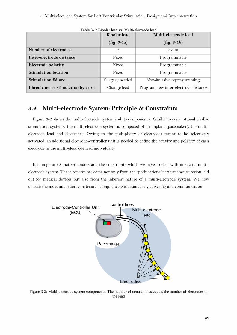
3. Multi-electrode System for Left Ventricular Stimulation: Design and Implementation
69
Table 3-1: Bipolar lead vs. Multi-electrode lead Bipolar lead
(fig. 3-1a)
Multi-electrode lead
(fig. 3-1b)
Number of electrodes 2 several
Inter-electrode distance Fixed Programmable
Electrode polarity Fixed Programmable
Stimulation location Fixed Programmable
Stimulation failure Surgery needed Non-invasive reprogramming
Phrenic nerve stimulation by error Change lead Program new inter-electrode distance
3.2 Multi-electrode System: Principle & Constraints
Figure 3-2 shows the multi-electrode system and its components. Similar to conventional cardiac
stimulation systems, the multi-electrode system is composed of an implant (pacemaker), the multi-
electrode lead and electrodes. Owing to the multiplicity of electrodes meant to be selectively
activated, an additional electrode-controller unit is needed to define the activity and polarity of each
electrode in the multi-electrode lead individually
It is imperative that we understand the constraints which we have to deal with in such a multi-
electrode system. These constraints come not only from the specifications/performance criterion laid
out for medical devices but also from the inherent nature of a multi-electrode system. We now
discuss the most important constraints: compliance with standards, powering and communication.
PacemakerPacemaker
Electrodes
control linesElectrode-Controller Unit
(ECU)Multi-electrode
lead
Figure 3-2: Multi-electrode system components. The number of control lines equals the number of electrodes in
the lead
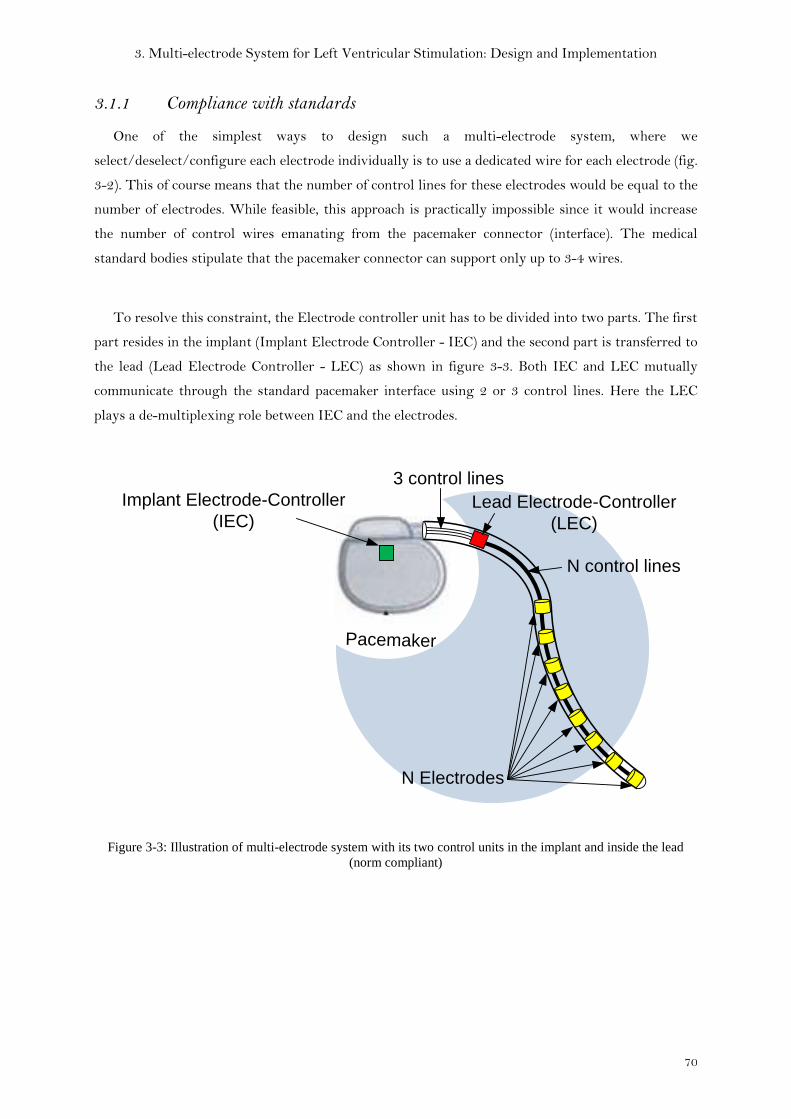
3. Multi-electrode System for Left Ventricular Stimulation: Design and Implementation
70
3.1.1 Compliance with standards
One of the simplest ways to design such a multi-electrode system, where we
select/deselect/configure each electrode individually is to use a dedicated wire for each electrode (fig.
3-2). This of course means that the number of control lines for these electrodes would be equal to the
number of electrodes. While feasible, this approach is practically impossible since it would increase
the number of control wires emanating from the pacemaker connector (interface). The medical
standard bodies stipulate that the pacemaker connector can support only up to 3-4 wires.
To resolve this constraint, the Electrode controller unit has to be divided into two parts. The first
part resides in the implant (Implant Electrode Controller - IEC) and the second part is transferred to
the lead (Lead Electrode Controller - LEC) as shown in figure 3-3. Both IEC and LEC mutually
communicate through the standard pacemaker interface using 2 or 3 control lines. Here the LEC
plays a de-multiplexing role between IEC and the electrodes.
PacemakerPacemaker
Lead Electrode-Controller
(LEC)
N Electrodes
3 control lines
Implant Electrode-Controller
(IEC)
N control lines
Figure 3-3: Illustration of multi-electrode system with its two control units in the implant and inside the lead
(norm compliant)
3. Multi-electrode System for Left Ventricular Stimulation: Design and Implementation
71
3.1.2 Communication protocol: Power and Configuration
Having chosen to employ a separate electrode-controller inside the lead to manage the multiple-
electrodes, we now face the obvious challenge of powering this electrode controller (LEC). Since this
LEC has to be placed inside a lead, the dimensions of this LEC have to be very small. Size constraints
therefore make it impossible to have on-board battery. We therefore chose to supply power to this
LEC by the pacemaker via a dedicated power line.
Since the IEC in the implant should control the LEC in order to configure/manage the electrodes, a
communication protocol is needed between the LEC and IEC.
Furthermore in order to minimize the number of wires, we chose to re-use the same wire (line) which
we had used for powering. The communication protocol adopted for our system will be discussed in
detail in section 3.4.3 of this chapter, but first we present the state of the art of such multi-electrode
systems.
3.3 State of the Art
The multi-electrode lead solution is under active research, with several pacemaker manufacturers
investigating different possibilities. Unfortunately most of the research exists as propriety
intellectual property.
By exploring the patents in the field of multi-electrode systems for cardiac pacemakers, we were
able to distinguish three different strategies followed for the implementation of IEC and LEC in
order to circumvent the aforementioned constraints. In this section we will summarize these three
strategies named: centralized structure, distributed structure and direct structure.
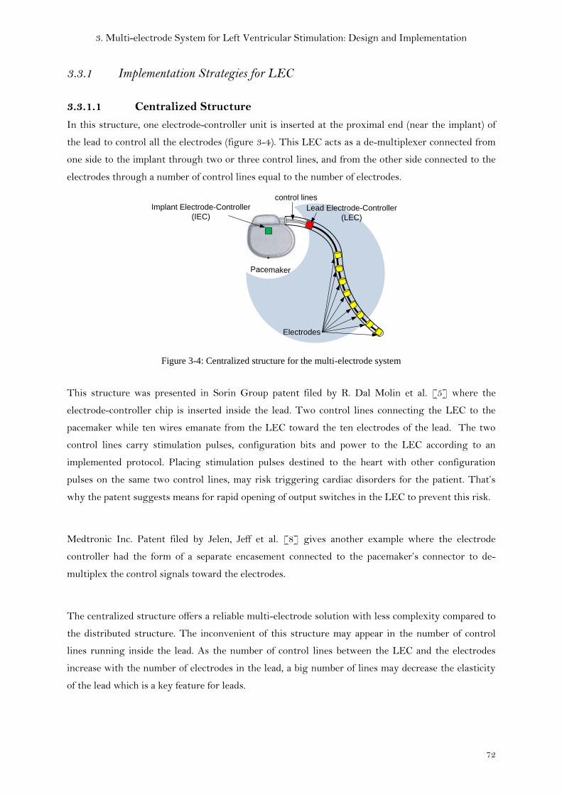
3. Multi-electrode System for Left Ventricular Stimulation: Design and Implementation
72
3.3.1 Implementation Strategies for LEC
3.3.1.1 Centralized Structure
In this structure, one electrode-controller unit is inserted at the proximal end (near the implant) of
the lead to control all the electrodes (figure 3-4). This LEC acts as a de-multiplexer connected from
one side to the implant through two or three control lines, and from the other side connected to the
electrodes through a number of control lines equal to the number of electrodes.
PacemakerPacemaker
Lead Electrode-Controller
(LEC)
Electrodes
control lines
Implant Electrode-Controller
(IEC)
Figure 3-4: Centralized structure for the multi-electrode system
This structure was presented in Sorin Group patent filed by R. Dal Molin et al. [5] where the
electrode-controller chip is inserted inside the lead. Two control lines connecting the LEC to the
pacemaker while ten wires emanate from the LEC toward the ten electrodes of the lead. The two
control lines carry stimulation pulses, configuration bits and power to the LEC according to an
implemented protocol. Placing stimulation pulses destined to the heart with other configuration
pulses on the same two control lines, may risk triggering cardiac disorders for the patient. That’s
why the patent suggests means for rapid opening of output switches in the LEC to prevent this risk.
Medtronic Inc. Patent filed by Jelen, Jeff et al. [8] gives another example where the electrode
controller had the form of a separate encasement connected to the pacemaker’s connector to de-
multiplex the control signals toward the electrodes.
The centralized structure offers a reliable multi-electrode solution with less complexity compared to
the distributed structure. The inconvenient of this structure may appear in the number of control
lines running inside the lead. As the number of control lines between the LEC and the electrodes
increase with the number of electrodes in the lead, a big number of lines may decrease the elasticity
of the lead which is a key feature for leads.
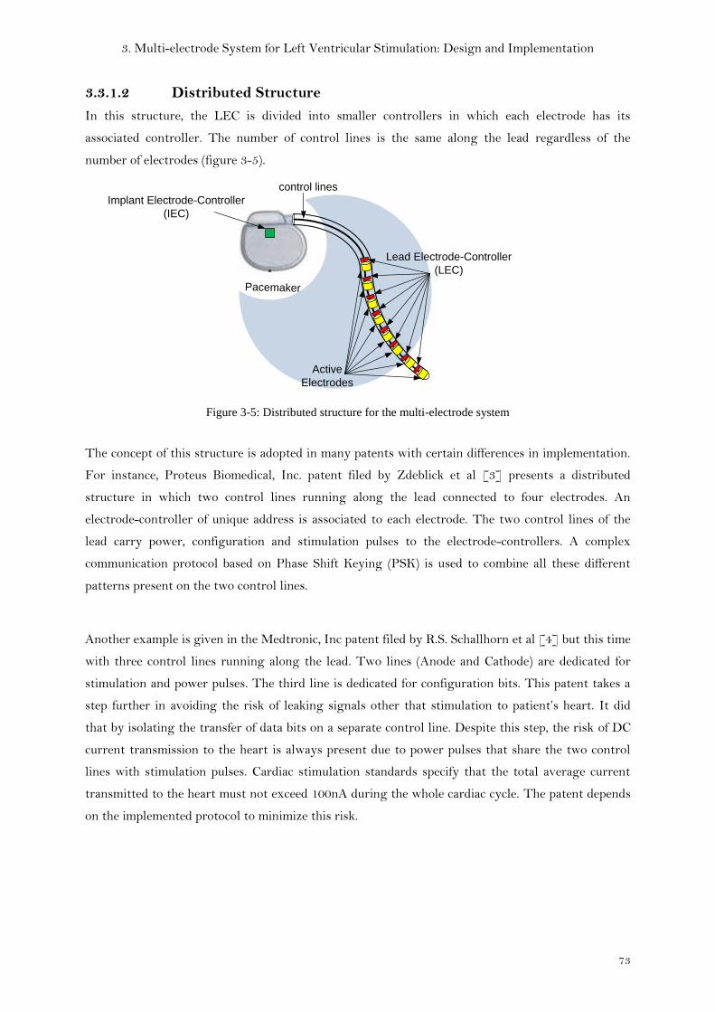
3. Multi-electrode System for Left Ventricular Stimulation: Design and Implementation
73
3.3.1.2 Distributed Structure
In this structure, the LEC is divided into smaller controllers in which each electrode has its
associated controller. The number of control lines is the same along the lead regardless of the
number of electrodes (figure 3-5).
PacemakerPacemaker
Lead Electrode-Controller
(LEC)
Active
Electrodes
control lines
Implant Electrode-Controller
(IEC)
Figure 3-5: Distributed structure for the multi-electrode system
The concept of this structure is adopted in many patents with certain differences in implementation.
For instance, Proteus Biomedical, Inc. patent filed by Zdeblick et al [3] presents a distributed
structure in which two control lines running along the lead connected to four electrodes. An
electrode-controller of unique address is associated to each electrode. The two control lines of the
lead carry power, configuration and stimulation pulses to the electrode-controllers. A complex
communication protocol based on Phase Shift Keying (PSK) is used to combine all these different
patterns present on the two control lines.
Another example is given in the Medtronic, Inc patent filed by R.S. Schallhorn et al [4] but this time
with three control lines running along the lead. Two lines (Anode and Cathode) are dedicated for
stimulation and power pulses. The third line is dedicated for configuration bits. This patent takes a
step further in avoiding the risk of leaking signals other that stimulation to patient’s heart. It did
that by isolating the transfer of data bits on a separate control line. Despite this step, the risk of DC
current transmission to the heart is always present due to power pulses that share the two control
lines with stimulation pulses. Cardiac stimulation standards specify that the total average current
transmitted to the heart must not exceed 100nA during the whole cardiac cycle. The patent depends
on the implemented protocol to minimize this risk.
3. Multi-electrode System for Left Ventricular Stimulation: Design and Implementation
74
3.3.1.3 Direct Structure
An exception was made by Saint Jude Medical in their quadripolar (4 electrodes) lead [9] where
they used a special 4-wire connector and directly controlled the lead electrodes by an IEC inside the
implant. In their solution the number of electrodes in the lead is constrained by the number of wires
that can be passed through the pacemaker connector.
3.4 System Design & Implementation
3.4.1 Adopted Strategy
Under our research project we wanted to test two strategies (Centralized and Distributed) in order
to adopt the best among them in terms of reliability and treatment efficiency. So we implemented the
LEC in the centralized structure with eight outputs to control eight electrodes in the lead.
Nevertheless, it can be used in a distributed structure by employing several LEC chips and activating
the unique address in the logic of each LEC chip. LEC logic is designed to switch between the
centralized and distributed modes through programming.
The support for dual mode functionality impacts the total size of the chip. Of course if the chip is to
be used in the distributed structure, there will be no need for eight outputs for the electrodes. But
only one output is sufficient to control one electrode in this case.
In order to avoid completely the risk of leaking electrical pulses to the heart other than the
stimulation pulses, we made the choice of using a 3-wire interface between the pacemaker connector
and the LEC. 2 wires (Anode and Cathode) are used exclusively for stimulation delivery and the
acquisition of cardiac signals. The third line is dedicated for the communication protocol between the
pacemaker (master) and the LEC (slave). This communication protocol carries power and
configuration bits needed for the LEC functionality. The advantage of this method that neither
power nor data are shared with the stimulation lines like the case of some patents cited before.
Moreover, we have committed ourselves to ensure the compatibility of our multi-electrode lead with
any pacemaker of the market, whether it supports the control of multi-electrode leads or not. We
took this further step by implementing an auxiliary switching unit in our LEC which has the role of
guarding an active connection between pacemaker and the patient’s heart through at least two
electrodes without any power consumption. This auxiliary unit permits also low power consumption
for the whole system as will be shown in section 3.4.2.6 of this chapter.
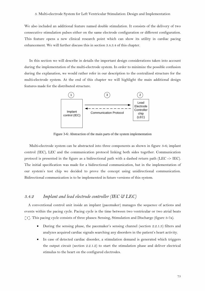
3. Multi-electrode System for Left Ventricular Stimulation: Design and Implementation
75
We also included an additional feature named double stimulation. It consists of the delivery of two
consecutive stimulation pulses either on the same electrode configuration or different configuration.
This feature opens a new clinical research point which can show its utility in cardiac pacing
enhancement. We will further discuss this in section 3.4.3.4 of this chapter.
In this section we will describe in details the important design considerations taken into account
during the implementation of the multi-electrode system. In order to minimize the possible confusion
during the explanation, we would rather refer in our description to the centralized structure for the
multi-electrode system. At the end of this chapter we will highlight the main additional design
features made for the distributed structure.
Implant
control (IEC)
Lead
Electrode
Controller
chip
(LEC)
1 3 2
Communication Protocol
Figure 3-6: Abstraction of the main parts of the system implementation
Multi-electrode system can be abstracted into three components as shown in figure 3-6; implant
control (IEC), LEC and the communication protocol linking both sides together. Communication
protocol is presented in the figure as a bidirectional path with a dashed return path (LEC -> IEC).
The initial specification was made for a bidirectional communication, but in the implementation of
our system’s test chip we decided to prove the concept using unidirectional communication.
Bidirectional communication is to be implemented in future versions of this system.
3.4.2 Implant and lead electrode controller (IEC & LEC)
A conventional control unit inside an implant (pacemaker) manages the sequence of actions and
events within the pacing cycle. Pacing cycle is the time between two ventricular or two atrial beats
[1]. This pacing cycle consists of three phases: Sensing, Stimulation and Discharge (figure 3-7a).
During the sensing phase, the pacemaker’s sensing channel (section 2.2.1.3) filters and
analyzes acquired cardiac signals searching any disorders in the patient’s heart activity.
In case of detected cardiac disorder, a stimulation demand is generated which triggers
the output circuit (section 2.2.1.2) to start the stimulation phase and deliver electrical
stimulus to the heart on the configured electrodes.
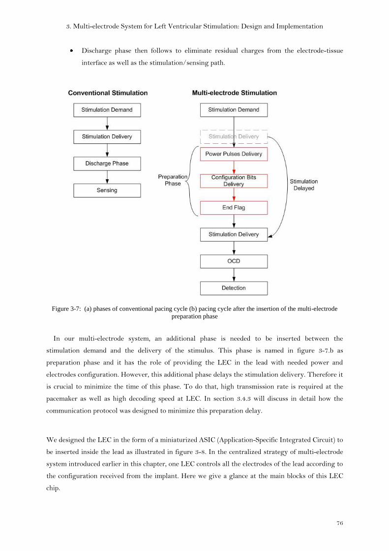
3. Multi-electrode System for Left Ventricular Stimulation: Design and Implementation
76
Discharge phase then follows to eliminate residual charges from the electrode-tissue
interface as well as the stimulation/sensing path.
Figure 3-7: (a) phases of conventional pacing cycle (b) pacing cycle after the insertion of the multi-electrode
preparation phase
In our multi-electrode system, an additional phase is needed to be inserted between the
stimulation demand and the delivery of the stimulus. This phase is named in figure 3-7.b as
preparation phase and it has the role of providing the LEC in the lead with needed power and
electrodes configuration. However, this additional phase delays the stimulation delivery. Therefore it
is crucial to minimize the time of this phase. To do that, high transmission rate is required at the
pacemaker as well as high decoding speed at LEC. In section 3.4.3 will discuss in detail how the
communication protocol was designed to minimize this preparation delay.
We designed the LEC in the form of a miniaturized ASIC (Application-Specific Integrated Circuit) to
be inserted inside the lead as illustrated in figure 3-8. In the centralized strategy of multi-electrode
system introduced earlier in this chapter, one LEC controls all the electrodes of the lead according to
the configuration received from the implant. Here we give a glance at the main blocks of this LEC
chip.
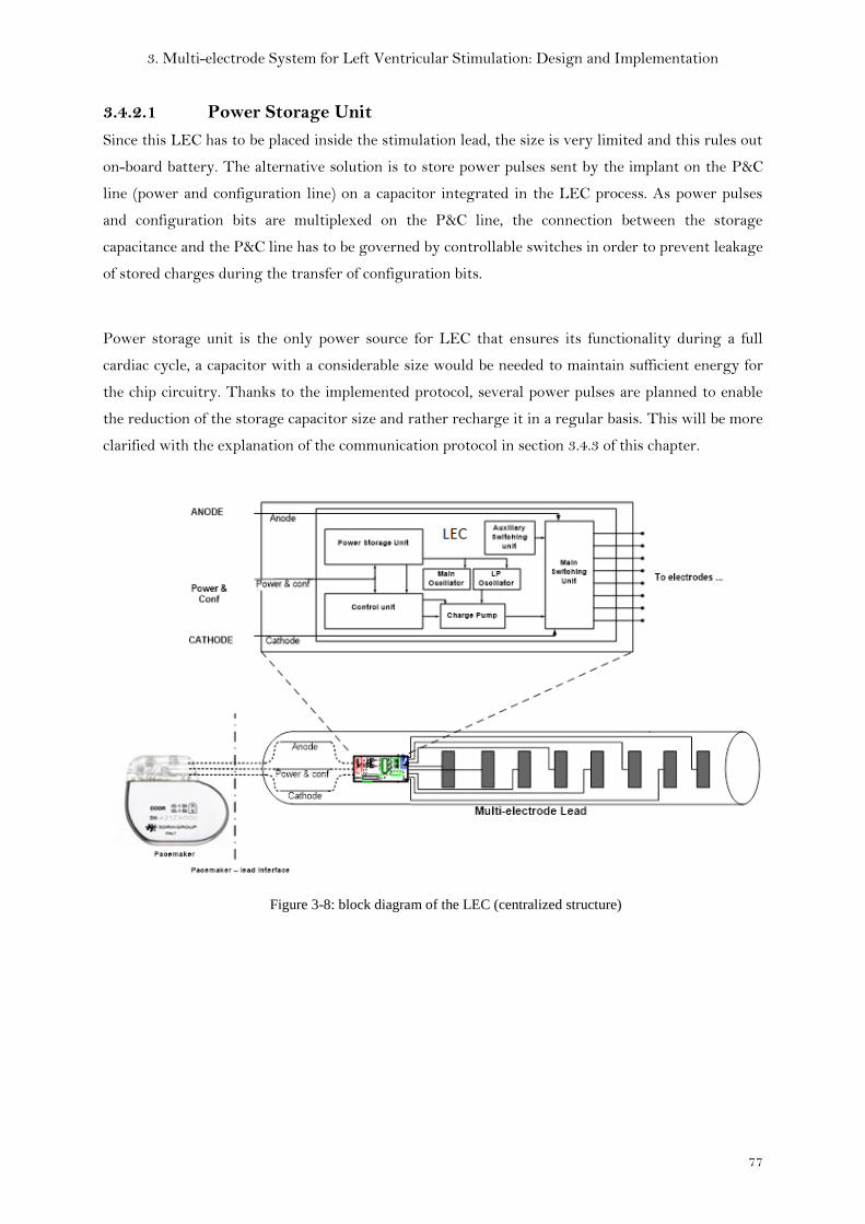
3. Multi-electrode System for Left Ventricular Stimulation: Design and Implementation
77
3.4.2.1 Power Storage Unit
Since this LEC has to be placed inside the stimulation lead, the size is very limited and this rules out
on-board battery. The alternative solution is to store power pulses sent by the implant on the P&C
line (power and configuration line) on a capacitor integrated in the LEC process. As power pulses
and configuration bits are multiplexed on the P&C line, the connection between the storage
capacitance and the P&C line has to be governed by controllable switches in order to prevent leakage
of stored charges during the transfer of configuration bits.
Power storage unit is the only power source for LEC that ensures its functionality during a full
cardiac cycle, a capacitor with a considerable size would be needed to maintain sufficient energy for
the chip circuitry. Thanks to the implemented protocol, several power pulses are planned to enable
the reduction of the storage capacitor size and rather recharge it in a regular basis. This will be more
clarified with the explanation of the communication protocol in section 3.4.3 of this chapter.
Figure 3-8: block diagram of the LEC (centralized structure)
3. Multi-electrode System for Left Ventricular Stimulation: Design and Implementation
78
3.4.2.2 Control Unit
LEC control unit is a custom-designed digital logic in which the communication protocol is
implemented. The first and essential role of this unit is to differentiate between power pulses and
configuration bits found on the P&C line. The control unit then routes power pulses to the power
storage unit, and internally decodes the configuration data bits. Control unit relies on local
oscillators to decode the timed digital configuration bits as well as the calculation of different delays
used within the communication protocol.
Moreover, the control unit activates both main and auxiliary switching units at precise moments
according to the decoded configuration data that indicate the desired state and polarity of each
electrode in the lead.
3.4.2.3 Oscillators
As we chose to implement a unidirectional communication protocol between the pacemaker (IEC)
and the LEC, the IEC does not receive any acknowledgements or resend demands from the LEC in
case of transmission errors. Therefore, timings have to be highly respected in order to ensure correct
functionality of the system. Oscillators are used to estimate the needed delays. But as the LEC has a
limited power source, the tradeoff between frequency precision and power consumption had to be
compromised. We chose local oscillators of +/- 5% tolerance. This tolerance increases the challenge
facing the communication protocol to take in account differences in frequency between master and
slave. Two local oscillators of different frequencies one of high and another of low frequency are used
in the LEC chip as follows:
Main Oscillator: runs at 1MHz frequency and used for rapid decoding of configuration bits.
The faster the decoding, the shorter the preparation phase inside the LEC that results in shorter
delay between stimulation demand and stimulation delivery as discussed earlier. It is also used in the
estimation of short delays in the communication protocol.
This high frequency oscillator is of considerable power consumption. Therefore it is disabled by the
end of the decoding phase. The low power oscillator continues to work till the end of the functional
cycle.
Low Power oscillator: runs at 32 KHz which has lower power consumption when compared to
the main oscillator. This oscillator is used at the end of the cardiac cycle to estimate the long delay
needed for the Discharge phase (13ms). This permits the LEC to function in a lower power mode till
the end of the cardiac cycle. Another block plays an important role in lowering the power
consumption of the LEC. This block is named auxiliary switching circuit and will be explained later
in this section.

3. Multi-electrode System for Left Ventricular Stimulation: Design and Implementation
79
3.4.2.4 OTP Memory
OTP or One Time Programmable memory is used to store trimming codes that correspond to the
most precise value for the oscillators’ frequency. These trimming codes are validated during the test
phase of the chip. Once validated, the codes are burned inside the OTP to ensure the stability of the
oscillators’ frequency.
3.4.2.5 Main Switching Unit
The “Main switching unit” defines the path of stimulation from the pacemaker to the heart, and it is
composed mainly of high voltage MOS switches in order to support the voltages (tens of volts) and
currents (tens of mA) of stimulation pulses delivered to the heart. The choice of a high-voltage
manufacturing technology was compulsory to support stimulation voltages and currents.
The path between the pacemaker and the configured electrodes has to be maintained by keeping the
configured MOS switches active. The control unit maintains this during stimulation and discharge
phases. During the sensing phase, the auxiliary switching unit takes over this role to transmit
cardiac signals to the pacemaker.
3.4.2.6 Auxiliary Switching Unit
By the end of the multi-electrode preparation phase, the LEC has performed its job in preparing
the stimulation path according to configuration chosen by the pacemaker. This is achieved after
correctly decoding configuration bits and activating correspondingly concerned electrodes through
the switching unit (HV MOS switches). LEC’s role extends beyond the preparation phase in order to
ensure the stability of configuration on its electrodes through maintaining the power on its
switching unit till the end of the pacing cycle.
An auxiliary switching unit is activated in the LEC when power level drops. This unit is able to
maintain the connection between electrodes and pacemaker without any power supply. In a first
implementation we used JFET switches. JFET switches are normally active while to disconnect
them a power is needed to force the inactive state. This auxiliary switching unit keeps the connection
between pacemaker and electrodes even when the LEC power vanishes. This is the case during the
sensing phase. It is difficult to estimate a fixed duration for this phase in order to size the storage
capacitance according to it.
Another advantage of using such an auxiliary switching unit is to ensure a compatibility with
any pacemaker implant found in the market. The fact that this auxiliary switching unit is
connected without power source, it ensures a minimal connection in the multi-electrode lead in order
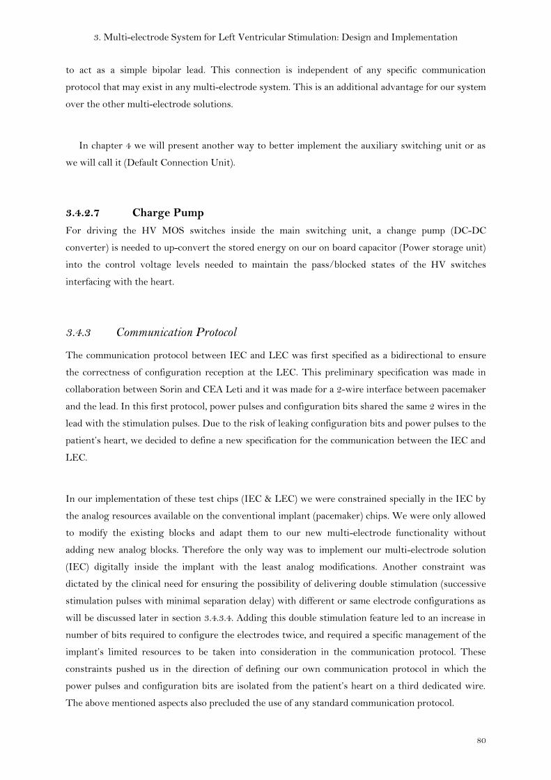
3. Multi-electrode System for Left Ventricular Stimulation: Design and Implementation
80
to act as a simple bipolar lead. This connection is independent of any specific communication
protocol that may exist in any multi-electrode system. This is an additional advantage for our system
over the other multi-electrode solutions.
In chapter 4 we will present another way to better implement the auxiliary switching unit or as
we will call it (Default Connection Unit).
3.4.2.7 Charge Pump
For driving the HV MOS switches inside the main switching unit, a change pump (DC-DC
converter) is needed to up-convert the stored energy on our on board capacitor (Power storage unit)
into the control voltage levels needed to maintain the pass/blocked states of the HV switches
interfacing with the heart.
3.4.3 Communication Protocol
The communication protocol between IEC and LEC was first specified as a bidirectional to ensure
the correctness of configuration reception at the LEC. This preliminary specification was made in
collaboration between Sorin and CEA Leti and it was made for a 2-wire interface between pacemaker
and the lead. In this first protocol, power pulses and configuration bits shared the same 2 wires in the
lead with the stimulation pulses. Due to the risk of leaking configuration bits and power pulses to the
patient’s heart, we decided to define a new specification for the communication between the IEC and
LEC.
In our implementation of these test chips (IEC & LEC) we were constrained specially in the IEC by
the analog resources available on the conventional implant (pacemaker) chips. We were only allowed
to modify the existing blocks and adapt them to our new multi-electrode functionality without
adding new analog blocks. Therefore the only way was to implement our multi-electrode solution
(IEC) digitally inside the implant with the least analog modifications. Another constraint was
dictated by the clinical need for ensuring the possibility of delivering double stimulation (successive
stimulation pulses with minimal separation delay) with different or same electrode configurations as
will be discussed later in section 3.4.3.4. Adding this double stimulation feature led to an increase in
number of bits required to configure the electrodes twice, and required a specific management of the
implant’s limited resources to be taken into consideration in the communication protocol. These
constraints pushed us in the direction of defining our own communication protocol in which the
power pulses and configuration bits are isolated from the patient’s heart on a third dedicated wire.
The above mentioned aspects also precluded the use of any standard communication protocol.
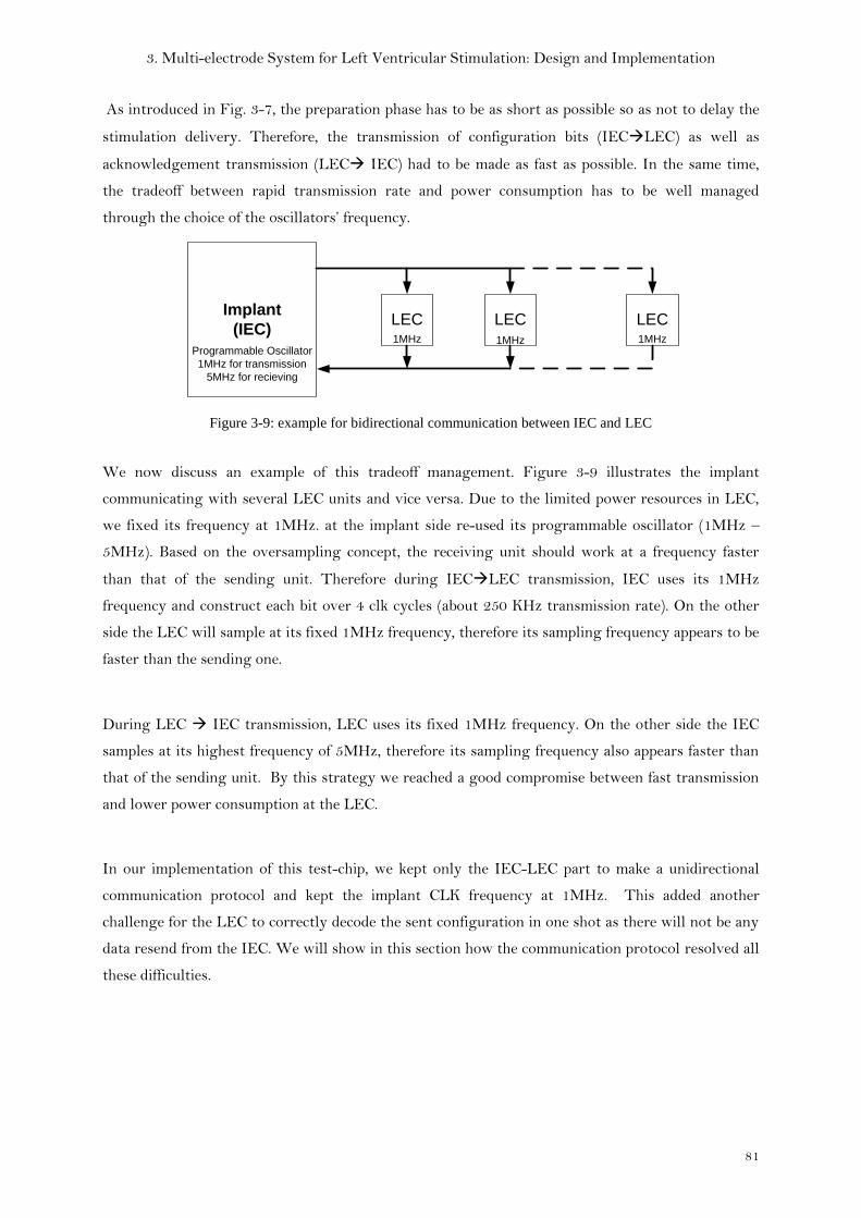
3. Multi-electrode System for Left Ventricular Stimulation: Design and Implementation
81
As introduced in Fig. 3-7, the preparation phase has to be as short as possible so as not to delay the
stimulation delivery. Therefore, the transmission of configuration bits (IECLEC) as well as
acknowledgement transmission (LEC IEC) had to be made as fast as possible. In the same time,
the tradeoff between rapid transmission rate and power consumption has to be well managed
through the choice of the oscillators’ frequency.
Implant
(IEC)LEC LEC LEC
Programmable Oscillator
1MHz for transmission
5MHz for recieving
1MHz 1MHz 1MHz
Figure 3-9: example for bidirectional communication between IEC and LEC
We now discuss an example of this tradeoff management. Figure 3-9 illustrates the implant
communicating with several LEC units and vice versa. Due to the limited power resources in LEC,
we fixed its frequency at 1MHz. at the implant side re-used its programmable oscillator (1MHz –
5MHz). Based on the oversampling concept, the receiving unit should work at a frequency faster
than that of the sending unit. Therefore during IECLEC transmission, IEC uses its 1MHz
frequency and construct each bit over 4 clk cycles (about 250 KHz transmission rate). On the other
side the LEC will sample at its fixed 1MHz frequency, therefore its sampling frequency appears to be
faster than the sending one.
During LEC IEC transmission, LEC uses its fixed 1MHz frequency. On the other side the IEC
samples at its highest frequency of 5MHz, therefore its sampling frequency also appears faster than
that of the sending unit. By this strategy we reached a good compromise between fast transmission
and lower power consumption at the LEC.
In our implementation of this test-chip, we kept only the IEC-LEC part to make a unidirectional
communication protocol and kept the implant CLK frequency at 1MHz. This added another
challenge for the LEC to correctly decode the sent configuration in one shot as there will not be any
data resend from the IEC. We will show in this section how the communication protocol resolved all
these difficulties.
3. Multi-electrode System for Left Ventricular Stimulation: Design and Implementation
82
We custom-designed our communication protocol at both ends: pacemaker and LEC. Pacemaker
plays the role of master in this protocol as it initiates the communication and provides power and
data. In return the LEC plays the role of slave and is required to manage power and to process
received data.
3rd
power
charge
Event
Synchro
Event
Synchro
1st
power
charge
Configuration
bits
2nd
power
charge
Discharge Phase
P&C
Cathode
… Sensing phase
Stimulation Trigger
Sensing phase ...
Communication Protocol
Delay
Stimulation
Phase
Figure 3-10: the different phases of the communication protocol
Firstly the pacemaker sends a first powering phase (fig. 3-10) to wake-up the LEC and activates its
circuitry. Once the LEC is activated, the pacemaker sends the configuration bits which informs the
LEC about the set of electrodes to be activated and their polarities. LEC decodes configuration bits
to extract this information then waits for pacemaker’s order (Event Synchronization) to activate
selected electrodes according to this configuration.
These “Event Synchronization” phases are planned with specific timing to synchronize the LEC
actions with events taking place in the pacemaker. Once the electrodes have been activated, the
stimulation is delivered to the cardiac tissues. We note here that these activated electrodes have to
maintain their configuration till the end of pacing cycle. Therefore additional power phases are also
planned to ensure sufficient power level in the LEC to maintain its configured state till the end of the
pacing cycle.
High transmission rate is required at pacemaker as well as high decoding speed at LEC. Two
independent local oscillators (LO) running at 1MHz are implemented, one at pacemaker and the
other at LEC. At such high frequency, the consumption in a power limited chip such as LEC is
considerable. We save power by deactivating the LEC’s 1MHz LO after the transmission of
configuration bits ends. Another low power oscillator in the LEC takes over till the end of pacing
cycle.
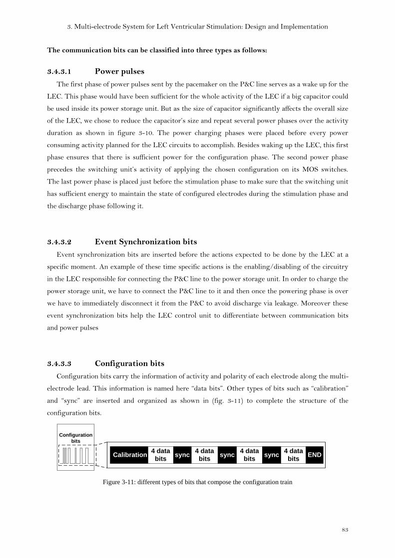
3. Multi-electrode System for Left Ventricular Stimulation: Design and Implementation
83
The communication bits can be classified into three types as follows:
3.4.3.1 Power pulses
The first phase of power pulses sent by the pacemaker on the P&C line serves as a wake up for the
LEC. This phase would have been sufficient for the whole activity of the LEC if a big capacitor could
be used inside its power storage unit. But as the size of capacitor significantly affects the overall size
of the LEC, we chose to reduce the capacitor’s size and repeat several power phases over the activity
duration as shown in figure 3-10. The power charging phases were placed before every power
consuming activity planned for the LEC circuits to accomplish. Besides waking up the LEC, this first
phase ensures that there is sufficient power for the configuration phase. The second power phase
precedes the switching unit’s activity of applying the chosen configuration on its MOS switches.
The last power phase is placed just before the stimulation phase to make sure that the switching unit
has sufficient energy to maintain the state of configured electrodes during the stimulation phase and
the discharge phase following it.
3.4.3.2 Event Synchronization bits
Event synchronization bits are inserted before the actions expected to be done by the LEC at a
specific moment. An example of these time specific actions is the enabling/disabling of the circuitry
in the LEC responsible for connecting the P&C line to the power storage unit. In order to charge the
power storage unit, we have to connect the P&C line to it and then once the powering phase is over
we have to immediately disconnect it from the P&C to avoid discharge via leakage. Moreover these
event synchronization bits help the LEC control unit to differentiate between communication bits
and power pulses
3.4.3.3 Configuration bits
Configuration bits carry the information of activity and polarity of each electrode along the multi-
electrode lead. This information is named here “data bits”. Other types of bits such as “calibration”
and “sync” are inserted and organized as shown in (fig. 3-11) to complete the structure of the
configuration bits.
Configuration
bits
Calibration4 data
bitssync
4 data
bitssync
4 data
bitssync
4 data
bitsEND
Figure 3-11: different types of bits that compose the configuration train
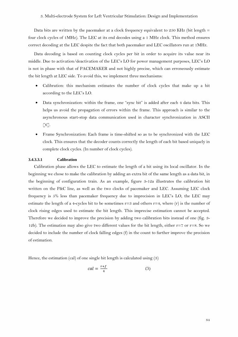
3. Multi-electrode System for Left Ventricular Stimulation: Design and Implementation
84
Data bits are written by the pacemaker at a clock frequency equivalent to 250 KHz (bit length =
four clock cycles of 1MHz). The LEC at its end decodes using a 1 MHz clock. This method ensures
correct decoding at the LEC despite the fact that both pacemaker and LEC oscillators run at 1MHz.
Data decoding is based on counting clock cycles per bit in order to acquire its value near its
middle. Due to activation/deactivation of the LEC’s LO for power management purposes, LEC’s LO
is not in phase with that of PACEMAKER and not highly precise, which can erroneously estimate
the bit length at LEC side. To avoid this, we implement three mechanisms:
Calibration: this mechanism estimates the number of clock cycles that make up a bit
according to the LEC’s LO.
Data synchronization: within the frame, one “sync bit” is added after each 4 data bits. This
helps us avoid the propagation of errors within the frame. This approach is similar to the
asynchronous start-stop data communication used in character synchronization in ASCII
[6].
Frame Synchronization: Each frame is time-shifted so as to be synchronized with the LEC
clock. This ensures that the decoder counts correctly the length of each bit based uniquely in
complete clock cycles. (In number of clock cycles).
3.4.3.3.1 Calibration
Calibration phase allows the LEC to estimate the length of a bit using its local oscillator. In the
beginning we chose to make the calibration by adding an extra bit of the same length as a data bit, in
the beginning of configuration train. As an example, figure 3-12a illustrates the calibration bit
written on the P&C line, as well as the two clocks of pacemaker and LEC. Assuming LEC clock
frequency is 5% less than pacemaker frequency due to imprecision in LEC’s LO, the LEC may
estimate the length of a 4-cycles bit to be sometimes r=3 and others r=4, where (r) is the number of
clock rising edges used to estimate the bit length. This imprecise estimation cannot be accepted.
Therefore we decided to improve the precision by adding two calibration bits instead of one (fig. 3-
12b). The estimation may also give two different values for the bit length, either r=7 or r=8. So we
decided to include the number of clock falling edges (f) in the count to further improve the precision
of estimation.
Hence, the estimation (cal) of one single bit length is calculated using (3)
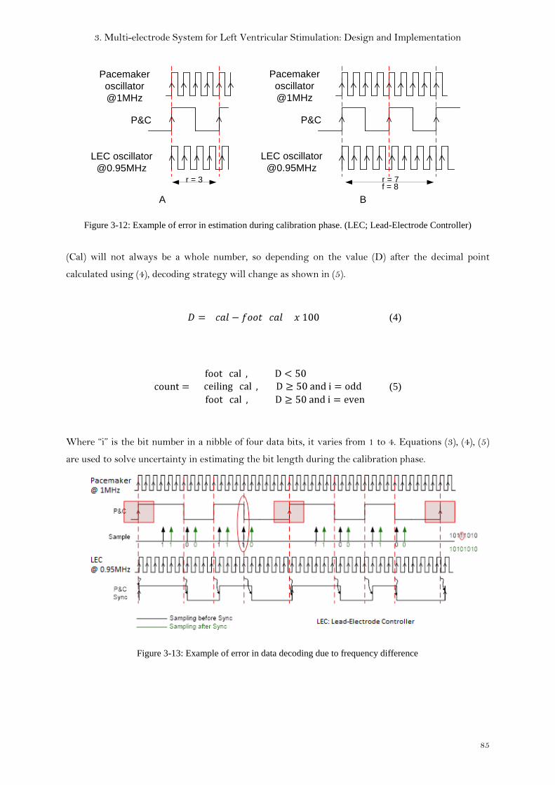
3. Multi-electrode System for Left Ventricular Stimulation: Design and Implementation
85
LEC oscillator
@0.95MHz
Pacemaker
oscillator
@1MHz
P&C
r = 7
LEC oscillator
@0.95MHz
Pacemaker
oscillator
@1MHz
P&C
r = 3
A B
f = 8
Figure 3-12: Example of error in estimation during calibration phase. (LEC; Lead-Electrode Controller)
(Cal) will not always be a whole number, so depending on the value (D) after the decimal point
calculated using (4), decoding strategy will change as shown in (5).
(4)
(5)
Where “i” is the bit number in a nibble of four data bits, it varies from 1 to 4. Equations (3), (4), (5)
are used to solve uncertainty in estimating the bit length during the calibration phase.
Figure 3-13: Example of error in data decoding due to frequency difference
3. Multi-electrode System for Left Ventricular Stimulation: Design and Implementation
86
3.4.3.3.2 Data Synchronization (Sync bits)
A Sync bit is a kind of delimiter inserted periodically every 4 data bits. Its form is always a low-to-
high transition (rising edge). Its role is to limit the propagation of any decoding error to the rest of
data. When the LEC’s control unit finishes decoding the first four data bits, it uses this sync bit to
reset the bit counter and starts counting to acquire the next 4 data bits.
To guarantee the maximum reliability of the decoding, a sync bit should be inserted after each data
bit. But it is unpractical if the number of bits is big as it doubles the time required for transmission.
The choice of the insertion frequency of sync bits in the configuration train was made in function of
the number of data bits in the train, data bit length and the time available for transmission.
3.4.3.3.3 Frame synchronization
After showing the importance of Calibration phase and Data Synchronization in ensuring correct
decoding, a third method has to be added (Frame synchronization). To understand its role we would
give an example in reference to (fig.3-13)
The upper signal (PACEMAKER@1MHz) represents the pacemaker’s clock running at 1MHz.
([email protected]) signal represents the LEC’s clock running at 0.95MHz to represent a frequency
difference of (-5%) in comparison with pacemaker’s clock frequency
(P&C) signal here shows a part of the configuration bits on the P&C line with three Sync bits
marked with red rectangles, and 4 data bits between each pair of Sync bits. According to calculations
made in (3) and (4), Calibration showed that bit length estimation is (cal = 3.75), therefore D = 75.
According to (5) the decoding strategy will be as follows: Starting from the rising edge of the 1st
sync bit, the decoder counts 4 clock cycles to acquire the value of the 1st data bit, then count 3 clock
cycles to acquire the value of the 2nd data bit, then count 4 clock cycles to acquire the value of the 3rd
data bit and finally counts 3 clock cycles to acquire the value of the 4th data bit. (i.e. counted 4 for odd
“i” and 3 for even “i”). The same sequence is repeated for the next four data bits after the 2nd sync bit
and so on till the end of data. Black arrows mark the positions where the values of data bits are
captured using the explained strategy. The error is caused by the dephasing between LEC’s clock
and pacemaker’s clock which resulted in counting an incomplete clock cycle as one. Added to this the
difference in frequencies, the error was propagated and appeared in the last bit in the first nibble
(circled in red).
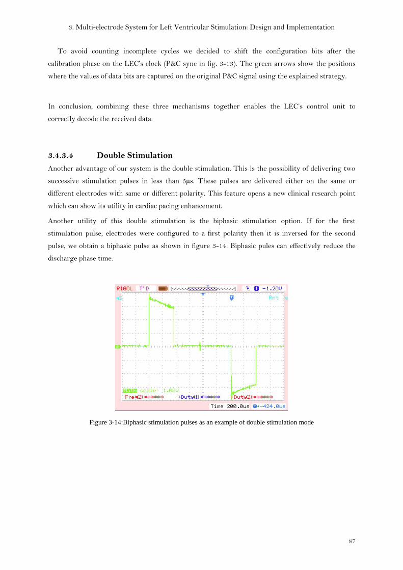
3. Multi-electrode System for Left Ventricular Stimulation: Design and Implementation
87
To avoid counting incomplete cycles we decided to shift the configuration bits after the
calibration phase on the LEC’s clock (P&C sync in fig. 3-13). The green arrows show the positions
where the values of data bits are captured on the original P&C signal using the explained strategy.
In conclusion, combining these three mechanisms together enables the LEC’s control unit to
correctly decode the received data.
3.4.3.4 Double Stimulation
Another advantage of our system is the double stimulation. This is the possibility of delivering two
successive stimulation pulses in less than 5µs. These pulses are delivered either on the same or
different electrodes with same or different polarity. This feature opens a new clinical research point
which can show its utility in cardiac pacing enhancement.
Another utility of this double stimulation is the biphasic stimulation option. If for the first
stimulation pulse, electrodes were configured to a first polarity then it is inversed for the second
pulse, we obtain a biphasic pulse as shown in figure 3-14. Biphasic pules can effectively reduce the
discharge phase time.
Figure 3-14:Biphasic stimulation pulses as an example of double stimulation mode
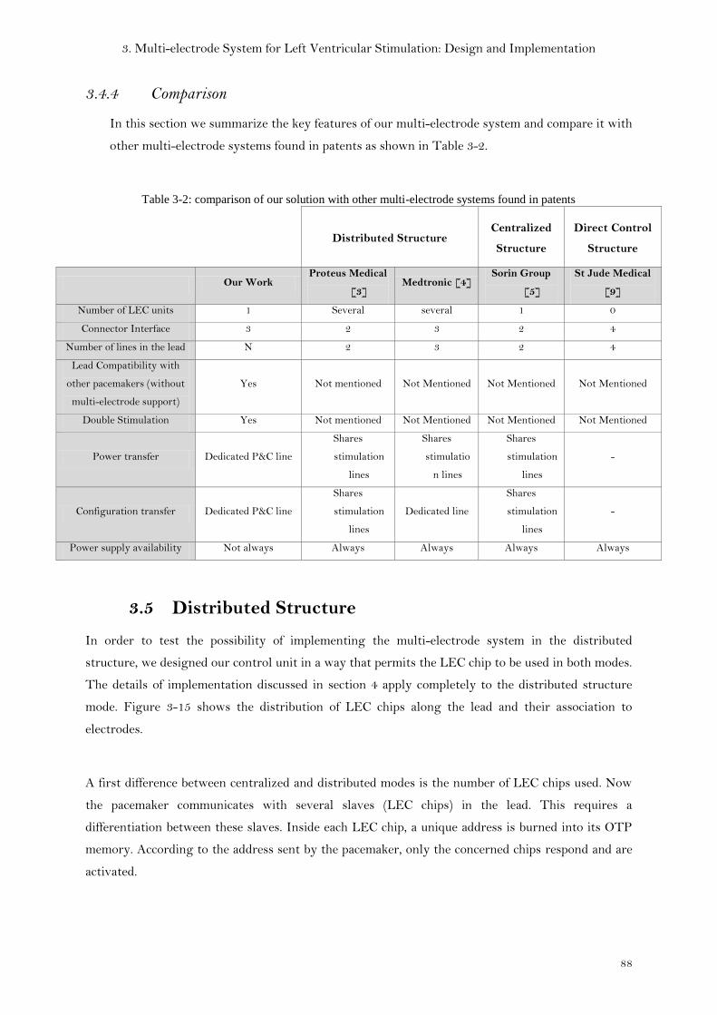
3. Multi-electrode System for Left Ventricular Stimulation: Design and Implementation
88
3.4.4 Comparison
4 In this section we summarize the key features of our multi-electrode system and compare it with
other multi-electrode systems found in patents as shown in Table 3-2.
Table 3-2: comparison of our solution with other multi-electrode systems found in patents
Distributed Structure Centralized
Structure
Direct Control
Structure
Our Work Proteus Medical
[3] Medtronic [4]
Sorin Group
[5]
St Jude Medical
[9]
Number of LEC units 1 Several several 1 0
Connector Interface 3 2 3 2 4
Number of lines in the lead N 2 3 2 4
Lead Compatibility with
other pacemakers (without
multi-electrode support)
Yes Not mentioned Not Mentioned Not Mentioned Not Mentioned
Double Stimulation Yes Not mentioned Not Mentioned Not Mentioned Not Mentioned
Power transfer Dedicated P&C line
Shares
stimulation
lines
Shares
stimulatio
n lines
Shares
stimulation
lines
-
Configuration transfer Dedicated P&C line
Shares
stimulation
lines
Dedicated line
Shares
stimulation
lines
-
Power supply availability Not always Always Always Always Always
3.5 Distributed Structure
In order to test the possibility of implementing the multi-electrode system in the distributed
structure, we designed our control unit in a way that permits the LEC chip to be used in both modes.
The details of implementation discussed in section 4 apply completely to the distributed structure
mode. Figure 3-15 shows the distribution of LEC chips along the lead and their association to
electrodes.
A first difference between centralized and distributed modes is the number of LEC chips used. Now
the pacemaker communicates with several slaves (LEC chips) in the lead. This requires a
differentiation between these slaves. Inside each LEC chip, a unique address is burned into its OTP
memory. According to the address sent by the pacemaker, only the concerned chips respond and are
activated.
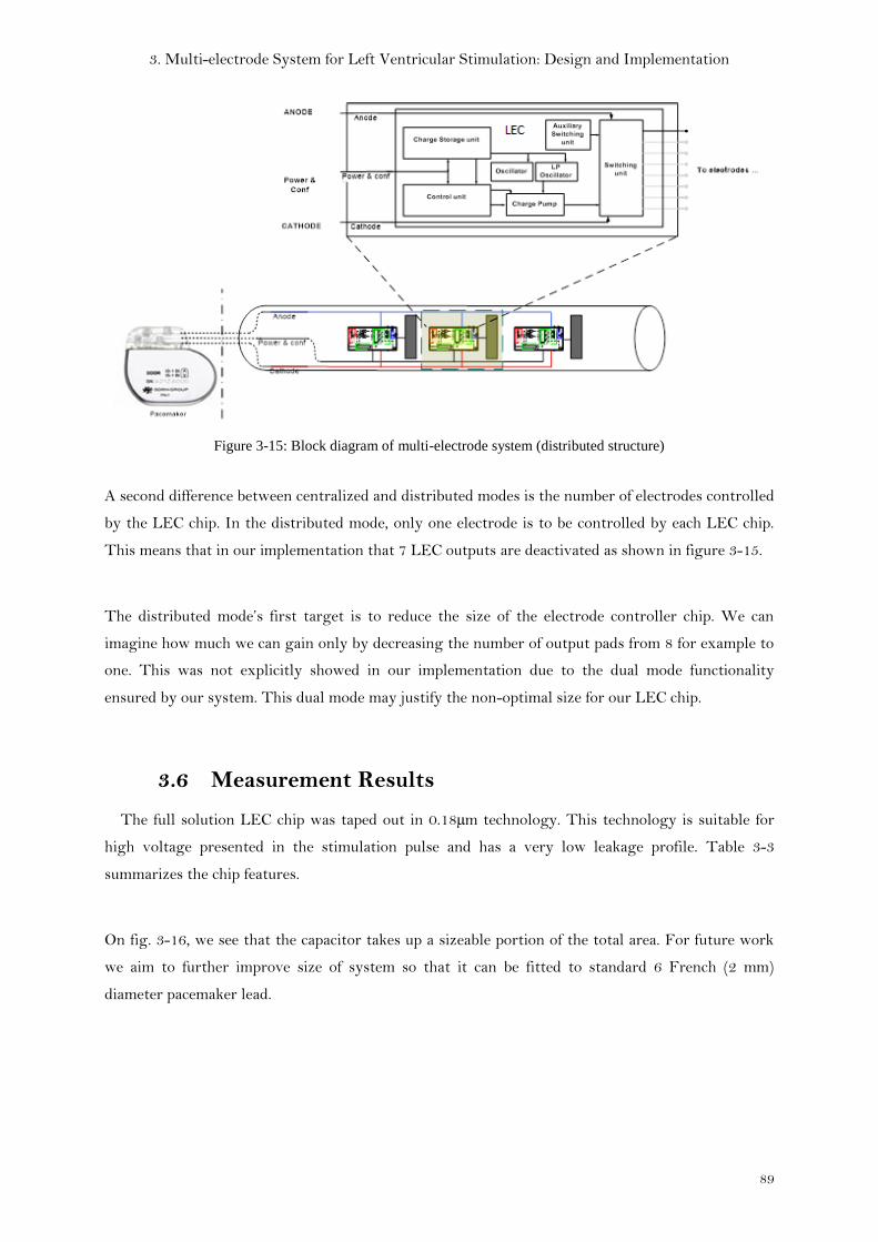
3. Multi-electrode System for Left Ventricular Stimulation: Design and Implementation
89
Figure 3-15: Block diagram of multi-electrode system (distributed structure)
A second difference between centralized and distributed modes is the number of electrodes controlled
by the LEC chip. In the distributed mode, only one electrode is to be controlled by each LEC chip.
This means that in our implementation that 7 LEC outputs are deactivated as shown in figure 3-15.
The distributed mode’s first target is to reduce the size of the electrode controller chip. We can
imagine how much we can gain only by decreasing the number of output pads from 8 for example to
one. This was not explicitly showed in our implementation due to the dual mode functionality
ensured by our system. This dual mode may justify the non-optimal size for our LEC chip.
3.6 Measurement Results
The full solution LEC chip was taped out in 0.18µm technology. This technology is suitable for
high voltage presented in the stimulation pulse and has a very low leakage profile. Table 3-3
summarizes the chip features.
On fig. 3-16, we see that the capacitor takes up a sizeable portion of the total area. For future work
we aim to further improve size of system so that it can be fitted to standard 6 French (2 mm)
diameter pacemaker lead.
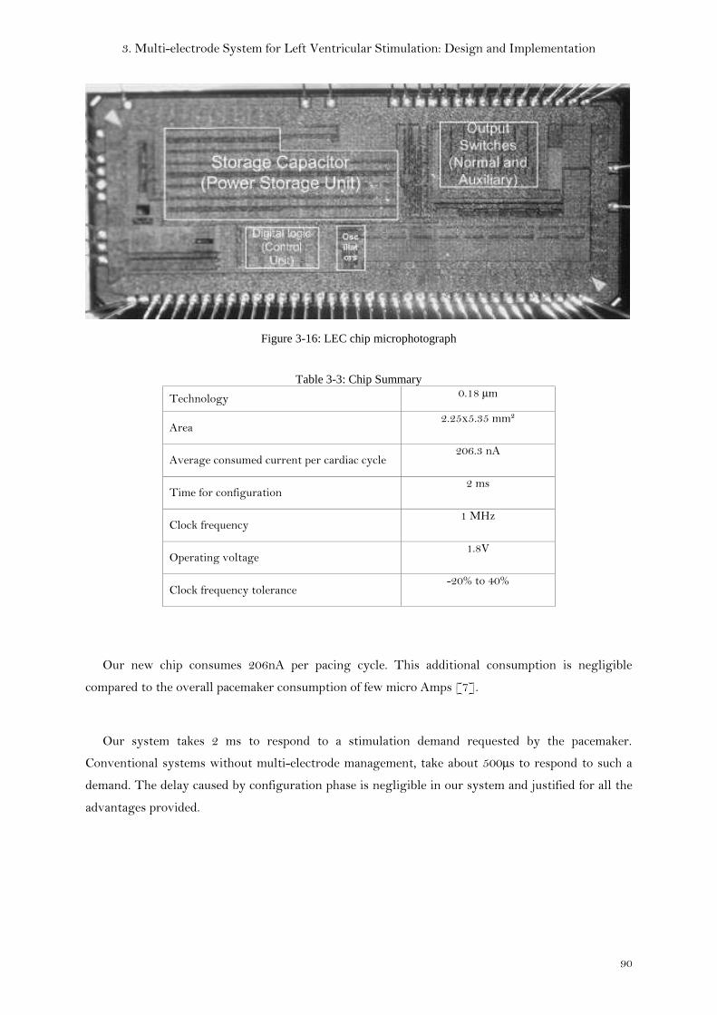
3. Multi-electrode System for Left Ventricular Stimulation: Design and Implementation
90
Figure 3-16: LEC chip microphotograph
Table 3-3: Chip Summary
Technology 0.18 µm
Area 2.25x5.35 mm²
Average consumed current per cardiac cycle 206.3 nA
Time for configuration 2 ms
Clock frequency 1 MHz
Operating voltage 1.8V
Clock frequency tolerance -20% to 40%
Our new chip consumes 206nA per pacing cycle. This additional consumption is negligible
compared to the overall pacemaker consumption of few micro Amps [7].
Our system takes 2 ms to respond to a stimulation demand requested by the pacemaker.
Conventional systems without multi-electrode management, take about 500µs to respond to such a
demand. The delay caused by configuration phase is negligible in our system and justified for all the
advantages provided.
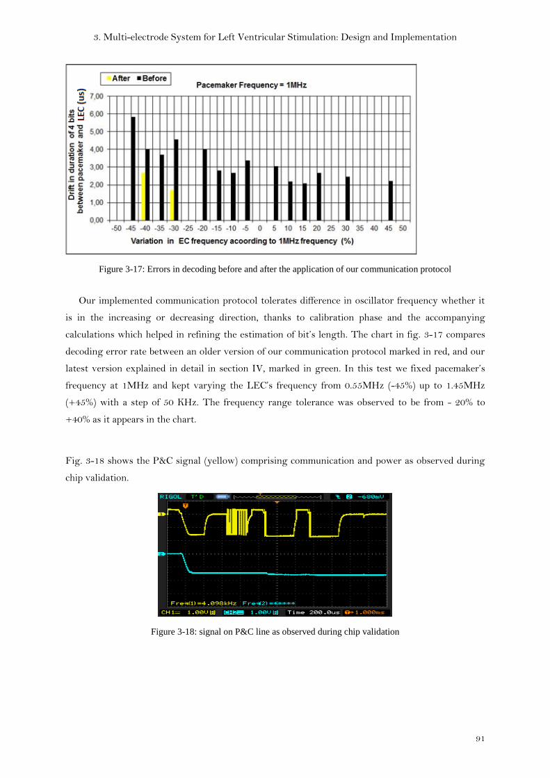
3. Multi-electrode System for Left Ventricular Stimulation: Design and Implementation
91
Figure 3-17: Errors in decoding before and after the application of our communication protocol
Our implemented communication protocol tolerates difference in oscillator frequency whether it
is in the increasing or decreasing direction, thanks to calibration phase and the accompanying
calculations which helped in refining the estimation of bit’s length. The chart in fig. 3-17 compares
decoding error rate between an older version of our communication protocol marked in red, and our
latest version explained in detail in section IV, marked in green. In this test we fixed pacemaker’s
frequency at 1MHz and kept varying the LEC’s frequency from 0.55MHz (-45%) up to 1.45MHz
(+45%) with a step of 50 KHz. The frequency range tolerance was observed to be from - 20% to
+40% as it appears in the chart.
Fig. 3-18 shows the P&C signal (yellow) comprising communication and power as observed during
chip validation.
Figure 3-18: signal on P&C line as observed during chip validation

3. Multi-electrode System for Left Ventricular Stimulation: Design and Implementation
92
3.7 Conclusion
In this chapter we presented the different design aspects for our multi-electrode system in its two
structures (centralized and distributed). We showed how we modified the implant’s control in order
to drive our custom-designed electrode-controller inserted inside the lead. The system helps in
overriding the limitations of left ventricular stimulation by adding more flexibility for the choice of
stimulation sites through its selective control of up to 8 electrodes with the possibility of
interchangeable polarity for each. The re-configurability of lead electrodes suppresses the need for
post-implant surgery in case of inhibition of patient response to stimulation caused by lead
displacement.
We implemented a one-wire communication protocol that tolerates difference in oscillator
frequencies between the implant and the electrode-controller. According to this protocol, power
pulses and configuration bits shared the same line, leaving Anode and Cathode lines for stimulation
and sensing purposes. This enabled the isolation of patient’s heart from data and power pulses.
Moreover it resulted in a norm-compliant 3-wire connector interface.
Our system is distinguished by ensuring compatibility of our multi-electrode lead with any
pacemaker in the market thanks its auxiliary switching unit. The concept was proved using discrete
JFET switches. In chapter 4 we will present a better solution named “Default Connection Unit” to be
integrated within the electrode-controller chip process.
Another notable feature in our system is its capability of delivering two consecutive stimulation
pulses of same or different polarities as configured. This feature enables biphasic stimulation which
may reduce the discharge period that follows the stimulation phase.
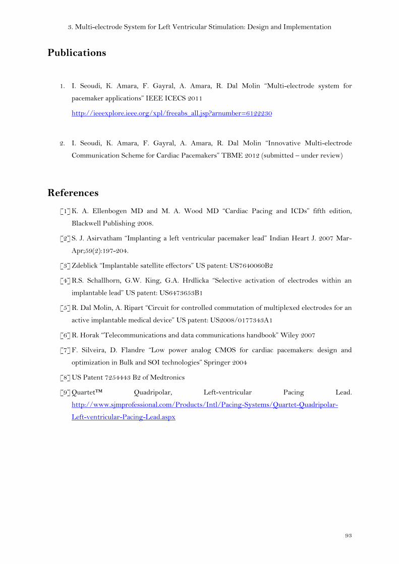
3. Multi-electrode System for Left Ventricular Stimulation: Design and Implementation
93
Publications
1. I. Seoudi, K. Amara, F. Gayral, A. Amara, R. Dal Molin “Multi-electrode system for
pacemaker applications” IEEE ICECS 2011
http://ieeexplore.ieee.org/xpl/freeabs_all.jsp?arnumber=6122230
2. I. Seoudi, K. Amara, F. Gayral, A. Amara, R. Dal Molin “Innovative Multi-electrode
Communication Scheme for Cardiac Pacemakers” TBME 2012 (submitted – under review)
References
[1] K. A. Ellenbogen MD and M. A. Wood MD “Cardiac Pacing and ICDs” fifth edition,
Blackwell Publishing 2008.
[2] S. J. Asirvatham “Implanting a left ventricular pacemaker lead” Indian Heart J. 2007 Mar-
Apr;59(2):197-204.
[3] Zdeblick “Implantable satellite effectors” US patent: US7640060B2
[4] R.S. Schallhorn, G.W. King, G.A. Hrdlicka “Selective activation of electrodes within an
implantable lead” US patent: US6473653B1
[5] R. Dal Molin, A. Ripart “Circuit for controlled commutation of multiplexed electrodes for an
active implantable medical device” US patent: US2008/0177343A1
[6] R. Horak “Telecommunications and data communications handbook” Wiley 2007
[7] F. Silveira, D. Flandre “Low power analog CMOS for cardiac pacemakers: design and
optimization in Bulk and SOI technologies” Springer 2004
[8] US Patent 7254443 B2 of Medtronics
[9] Quartet™ Quadripolar, Left-ventricular Pacing Lead.
http://www.sjmprofessional.com/Products/Intl/Pacing-Systems/Quartet-Quadripolar-
Left-ventricular-Pacing-Lead.aspx

4. Default Connection Unit
94
4. Default Connection Unit
95
4 Chapter 4
Default Connection Unit

4. Default Connection Unit
96
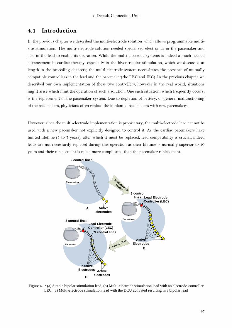
4. Default Connection Unit
97
4.1 Introduction
In the previous chapter we described the multi-electrode solution which allows programmable multi-
site stimulation. The multi-electrode solution needed specialized electronics in the pacemaker and
also in the lead to enable its operation. While the multi-electrode systems is indeed a much needed
advancement in cardiac therapy, especially in the biventricular stimulation, which we discussed at
length in the preceding chapters; the multi-electrode system necessitates the presence of mutually
compatible controllers in the lead and the pacemaker(the LEC and IEC). In the previous chapter we
described our own implementation of these two controllers, however in the real world, situations
might arise which limit the operation of such a solution. One such situation, which frequently occurs,
is the replacement of the pacemaker system. Due to depletion of battery, or general malfunctioning
of the pacemakers, physicians often replace the implanted pacemakers with new pacemakers.
However, since the multi-electrode implementation is proprietary, the multi-electrode lead cannot be
used with a new pacemaker not explicitly designed to control it. As the cardiac pacemakers have
limited lifetime (5 to 7 years), after which it must be replaced, lead compatibility is crucial, indeed
leads are not necessarily replaced during this operation as their lifetime is normally superior to 10
years and their replacement is much more complicated than the pacemaker replacement.
Pacemaker
PacemakerPacemaker
Pacemaker
Lead Electrode-
Controller (LEC)
N control lines
Active
Electrodes
Lead Electrode-
Controller (LEC)
3 control
lines
3 control lines
Active
electrodes
Inactive
Electrodes
2 control lines
Active
electrodes
Multi-electrode
solution
Activatin
g DCU
A.
B.
C.
Figure 4-1: (a) Simple bipolar stimulation lead, (b) Multi-electrode stimulation lead with an electrode-controller
LEC, (c) Multi-electrode stimulation lead with the DCU activated resulting in a bipolar lead
4. Default Connection Unit
98
In the multi-electrode solution presented in chapter 3, several electrodes were inserted along the
stimulation lead connected to an electrode-controller (LEC) at one end of the lead. The LEC
configures the multi-electrode lead, by selectively enabling the appropriate electrodes and choosing
their polarity (cathode or anode). Since LEC inside the lead obtains this configuration information
from the pacemaker, the LEC effectively acts as an interface between the Pacemaker and the
electrodes (Fig. 4-1b). A specific power and communication protocol was implemented partially in
the LEC and partially in the pacemaker.
In this chapter we present a solution to solve the lead compatibility problem by adding a switching
structure to the existing LEC. This switching structure, called DCU (Default Connection Unit),
allows the multi-electrode lead to function as a standard bipolar lead (fig. 4-1c) without the need for
additional configuration or power supply. DCU is designed to be autonomous and independent of any
communication protocols between pacemaker and LEC.
The key features of the DCU can be resumed in three points:
a) “Normally-ON” switch,
b) Low Ron resistance,
c) Can be disabled (turned off) when needed.
We first addressed the lead compatibility problem by using the auxiliary switching unit as
presented in chapter 3. JFET switches were used as discrete components in the auxiliary switching
unit to prove the concept. Even though some of the features brought by the DCU can be fulfilled by
alternate technologies such as JFET, depleted MOS, etc., these technologies are generally not
available in process technologies used by medical device industry (pacemakers etc.)
Our DCU structure can be adapted to any process as it is based on ordinary MOS transistors and
therefore presents a versatile solution. Other solutions on the other hand were only available as
discrete components and hence were unviable owing to size constraints of the LEC chip.
4.2 Design Challenges and Choices
Figure 4-2 shows the block diagram of the LEC which houses the DCU and its interfaces with
pacemaker and electrodes. In the dedicated stimulation lead, since the needed energy for LEC chip
could not be recovered from the anode and cathode only, power is supplied to the LEC chip by using
an additional cable (P&C line in fig. 4-2 to transfer power pulses and configuration bits [1]. This
transfer is done using a specific protocol between LEC and pacemaker which is then decoded by the

4. Default Connection Unit
99
LEC’s control unit [1]. The anode and cathode lines carry the stimulation energy from pacemaker to
the electrodes.
Pacemaker
Pacemaker – lead interface
Left Ventricular Lead
To
Ele
ctro
de
s
EN
ENX
Switching
unit
Default
connection
unit
Anode
P&C
Cathode
Charge
Storage unit
Control
Unit
Oscillator
Charge
Pump
LEC
e1
e2
Figure 4-2: Lead Electrode Controller blockdiagram including the DCU
Despite the fact that the DCU is integrated inside the LEC, they function alternatively as
described in table 4-1. Since the P&C line is also used for communication besides powering, a specific
protocol had to be devised to that effect. Furthermore since DCU is active when LEC is inactive, it
renders the DCU transparent to any such protocol mechanism between LEC and pacemaker.
Therefore, P&C line cannot be used to provide the DCU with needed power as it is the case with
LEC. Hence, the DCU was designed to use available energy on Anode and Cathode to power itself.
Table 4-1: Operation modes
LEC DCU
Multi-electrode mode (Fig. 4-1b) Active Inactive
Default mode (Fig. 4-1c) Inactive Active
The amount of energy available on the Anode and Cathode varies in each phase of the
pacemaker’s pacing cycle. Pacing cycle consists of three phases named “Stimulation”, “Discharge” and
“Sensing” [1]. During the “Stimulation” phase Anode & Cathode carry the stimulation pulse from
the pacemaker to the selected electrodes. This stimulation pulse has amplitude that varies from -2V
to -8V for a maximum duration of 1ms. During the “Discharge” phase, residual charges on the
electrode-tissue interface is drained through Anode & Cathode. This discharge voltage reaches
approximately +1V for a duration of tens of milliseconds. During the “Sensing” phase, Anode &
Cathode carry the sensed cardiac signals from selected electrodes back to the pacemaker in order to
enable the monitoring of the patient’s state. Cardiac signals have amplitude of tens of millivolts
which is very weak compared to the stimulation amplitude. The “Sensing” phase duration can vary
from several seconds to several minutes, depending on the patient’s need for stimulation.
4. Default Connection Unit
100
The energy source is available exclusively during the “Stimulation” phase, which lasts for a
maximum of 1ms, while the DCU must function for seconds or even minutes depending on the
duration of “Discharge” and “Sensing” phases. As we will show in section 3, the DCU was designed
to use this limited power source and function reliably for the entire pacing cycle.
4.3 DCU Operation Principle
As described in table 4-1, DCU operates in the default mode when LEC is inactive. Figure 4-2
illustrates the position of DCU inside the LEC chip. DCU has four inputs (Anode, Cathode, EN and
ENX) and two outputs (e1 and e2). EN & ENX are control signals generated by the LEC’s control
unit in order to activate/deactivate the DCU. The outputs e1 and e2 are connected to two of the
electrodes in the multi-electrode lead. These two electrodes are named hereafter (default electrodes).
These default electrodes are shared between the LEC’s switching unit and the DCU. Note that when
DCU is active, it takes full control of the default electrodes (LEC is inactive). Despite the fact that
the LEC is inactive along with its control unit responsible for EN & ENX generation, these signals
are set to values that enable DCU through a power-on-reset circuit which detects the presence of
power on Anode and Cathode during stimulation phase.
4.4 System Implementation
The DCU when activated creates two connections between its inputs and its outputs. One
between Anode & E1 and the other between Cathode & E2. These connections are marked in (fig. 4-
3) as “Path1” and “Path2”. Both paths have to be maintained during the three phases of the pacing
cycle described before. When the DCU is deactivated, it has to cut the connections of both path1 and
path2. We now describe the DCU circuitry implemented to achieve this function
4.4.1 Architecture
We will start by describing the DCU behavior in its active state during the different phases of
pacing cycle. “Path 1” is formed by two PMOS transistors M1 and M2, connected back-to-back.
Similarly, “Path 2” is formed by two NMOS transistors M4 and M5, connected back-to-back.
Transistors of both paths are sized for low RON, to meet the specification of switches conventionally
used for similar purposes in pacemakers. As we remarked that Cathode & Anode inputs may change
their polarities or fluctuate during the different phases of the pacing cycle, therefore, “relative
voltage difference” between them is needed to drive the transistors

4. Default Connection Unit
101
Path 1
Path 2
ENX
ENX
Figure 4-3: DCU circuit
This is achieved through the MIN–MAX generator (fig. 4-3). The MIN–MAX generator as the
name suggests, does a relative comparison of cathode & anode inputs and produces the maximum
(MAX) and minimum (MIN) of these as outputs. The circuit of MAX-MIN generator is given in
figure 4-4. M7 and M8 PMOS are connected as such to generate the maximum voltage found
between Anode and Cathode. Similarly M9 and M10 NMOS generate the minimum voltage found
between Anode and Cathode.
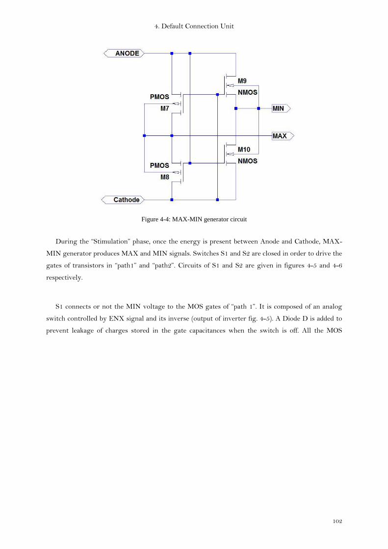
4. Default Connection Unit
102
Figure 4-4: MAX-MIN generator circuit
During the “Stimulation” phase, once the energy is present between Anode and Cathode, MAX-
MIN generator produces MAX and MIN signals. Switches S1 and S2 are closed in order to drive the
gates of transistors in “path1” and “path2”. Circuits of S1 and S2 are given in figures 4-5 and 4-6
respectively.
S1 connects or not the MIN voltage to the MOS gates of “path 1”. It is composed of an analog
switch controlled by ENX signal and its inverse (output of inverter fig. 4-5). A Diode D is added to
prevent leakage of charges stored in the gate capacitances when the switch is off. All the MOS
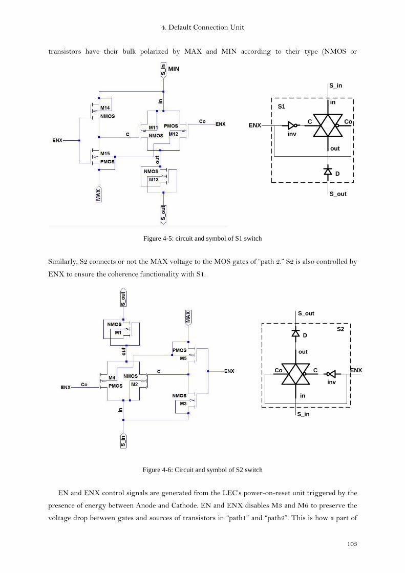
4. Default Connection Unit
103
transistors have their bulk polarized by MAX and MIN according to their type (NMOS or
in
out
CoC
D
inv
ENX
MIN
S_out
S_in
S1
Figure 4-5: circuit and symbol of S1 switch
Similarly, S2 connects or not the MAX voltage to the MOS gates of “path 2.” S2 is also controlled by
ENX to ensure the coherence functionality with S1.
out
in
CCo
D
inv
ENX
S_out
S_in
S2
Figure 4-6: Circuit and symbol of S2 switch
EN and ENX control signals are generated from the LEC’s power-on-reset unit triggered by the
presence of energy between Anode and Cathode. EN and ENX disables M3 and M6 to preserve the
voltage drop between gates and sources of transistors in “path1” and “path2”. This is how a part of
4. Default Connection Unit
104
the stimulation energy was used to turn ON “Path1” and “Path2”, thereby eliminating the need for
an external power source.
During “Discharge” phase, the DCU must retain its connected state in order to allow the
discharge of residual charges through a high conductance path; otherwise the discharging takes
considerable duration. However since during the “Discharge” phase, there is no voltage difference
between the anode and cathode lines, unlike during the “Stimulation” phase, we need to find a way to
keep the transistors in the ON state. We did so by using the gate capacitances present in M1-M2 and
M4-M5 to store energy during the stimulation and maintain it during the limited duration of the
“Discharge” phase. We discuss the sizing issues connected to gate capacitances in the following
subsection. In order to avoid the leakage of charge stored in the gate capacitances, S1 and S2 are
automatically opened immediately after the “Stimulation” phase.
During the “Sensing” phase, DCU must retain a connected path to transfer cardiac signals from
electrodes to the pacemaker. As discussed in section II, the duration of the “Sensing” phase is
unpredictable and depends on the patient’s need. Since capacitances cannot be sized for unpredictable
retention durations it is not feasible to use the technique employed in the “Discharge” phase. In this
case we chose to ensure this connection by using resistors (R1, R2) of the order of kΩ (fig. 4-4). The
resistance values were judiciously chosen to prevent the passage of electrical signals during
“Stimulation” and “Discharge” phases while ensuring the passage of cardiac signals. R1 and R2 have
to be large compared to cardiac muscle resistance between electrodes (300 ohms typically) and small
compared to sensing channel input resistance (100 kilo-ohm typically).
Finally, DCU can be deactivated when the LEC is active. This is done by activating M3 and M6
(fig. 4-4) through the control of EN and ENX signals. These two transistors when activated, short
circuit the gates and sources of M1-M2 and M4-M5, and block the connection between “default
electrodes” and pacemaker. The back-to-back connection between each couple of transistors M1-M2
and M4-M5 enhances the DCU OFF state. This justifies the choice of using two transistors per path
and not just one.
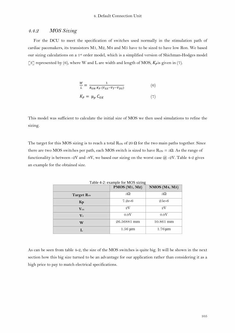
4. Default Connection Unit
105
4.4.2 MOS Sizing
For the DCU to meet the specification of switches used normally in the stimulation path of
cardiac pacemakers, its transistors M1, M2, M4 and M5 have to be sized to have low Ron. We based
our sizing calculations on a 1st order model, which is a simplified version of Shichman-Hodges model
[3] represented by (6), where W and L are width and length of MOS, is given in (7).
(6)
(7)
This model was sufficient to calculate the initial size of MOS we then used simulations to refine the
sizing.
The target for this MOS sizing is to reach a total RON of 20 Ω for the two main paths together. Since
there are two MOS switches per path, each MOS switch is sized to have RON = 5Ω. As the range of
functionality is between -2V and -8V, we based our sizing on the worst case @ -2V. Table 4-2 gives
an example for the obtained size.
Table 4-2: example for MOS sizing
PMOS (M1, M2) NMOS (M4, M5)
Target RON 5Ω 5Ω
Kp 7.2e-6 25e-6
VGS 2V 2V
VT 0.9V 0.9V
W 26.56881 mm 10.861 mm
L 1.56 µm 1.76 µm
As can be seen from table 4-2, the size of the MOS switches is quite big. It will be shown in the next
section how this big size turned to be an advantage for our application rather than considering it as a
high price to pay to match electrical specifications.
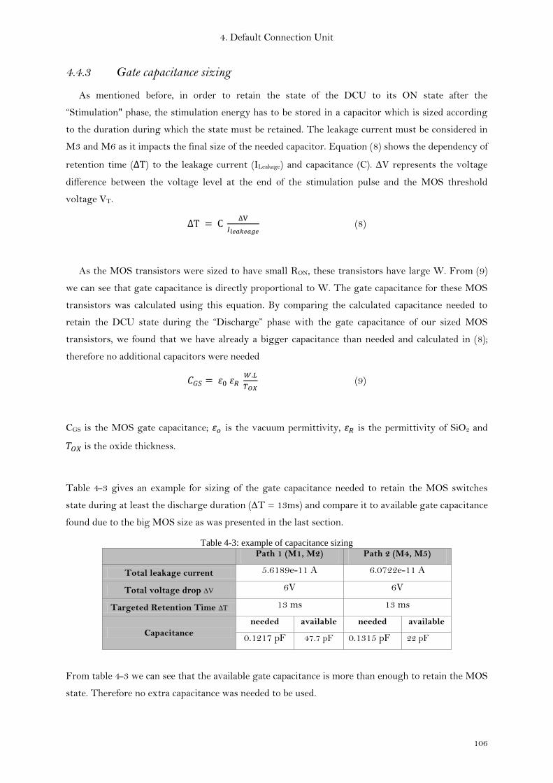
4. Default Connection Unit
106
4.4.3 Gate capacitance sizing
As mentioned before, in order to retain the state of the DCU to its ON state after the
“Stimulation" phase, the stimulation energy has to be stored in a capacitor which is sized according
to the duration during which the state must be retained. The leakage current must be considered in
M3 and M6 as it impacts the final size of the needed capacitor. Equation (8) shows the dependency of
retention time ( ) to the leakage current (ILeakage) and capacitance (C). ∆V represents the voltage
difference between the voltage level at the end of the stimulation pulse and the MOS threshold
voltage VT.
(8)
As the MOS transistors were sized to have small RON, these transistors have large W. From (9)
we can see that gate capacitance is directly proportional to W. The gate capacitance for these MOS
transistors was calculated using this equation. By comparing the calculated capacitance needed to
retain the DCU state during the “Discharge” phase with the gate capacitance of our sized MOS
transistors, we found that we have already a bigger capacitance than needed and calculated in (8);
therefore no additional capacitors were needed
(9)
CGS is the MOS gate capacitance; is the vacuum permittivity, is the permittivity of SiO2 and
is the oxide thickness.
Table 4-3 gives an example for sizing of the gate capacitance needed to retain the MOS switches
state during at least the discharge duration (∆T = 13ms) and compare it to available gate capacitance
found due to the big MOS size as was presented in the last section.
Table 4-3: example of capacitance sizing
Path 1 (M1, M2) Path 2 (M4, M5)
Total leakage current 5.6189e-11 A 6.0722e-11 A
Total voltage drop ∆V 6V 6V
Targeted Retention Time ∆T 13 ms 13 ms
Capacitance
needed available needed available
0.1217 pF 47.7 pF 0.1315 pF 22 pF
From table 4-3 we can see that the available gate capacitance is more than enough to retain the MOS
state. Therefore no extra capacitance was needed to be used.
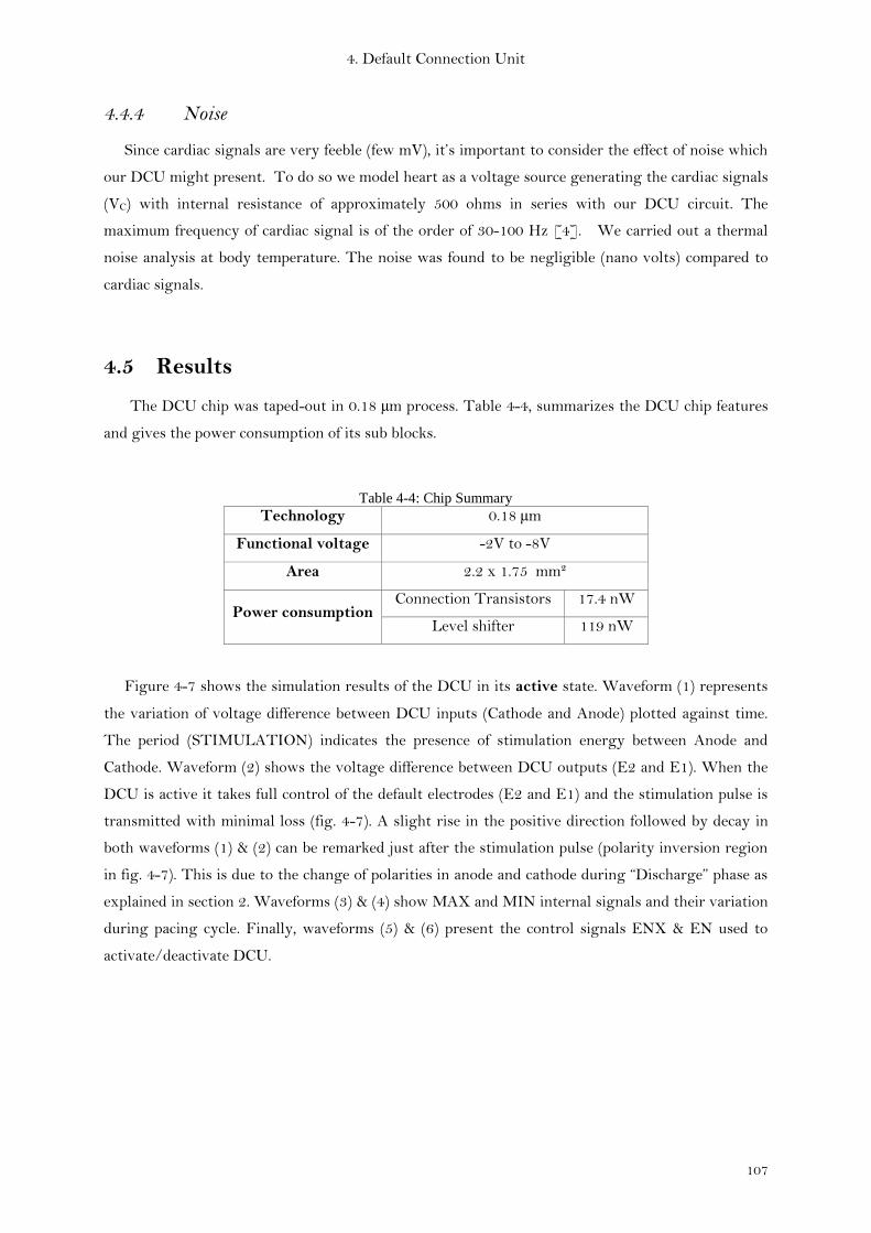
4. Default Connection Unit
107
4.4.4 Noise
Since cardiac signals are very feeble (few mV), it’s important to consider the effect of noise which
our DCU might present. To do so we model heart as a voltage source generating the cardiac signals
(VC) with internal resistance of approximately 500 ohms in series with our DCU circuit. The
maximum frequency of cardiac signal is of the order of 30-100 Hz [4]. We carried out a thermal
noise analysis at body temperature. The noise was found to be negligible (nano volts) compared to
cardiac signals.
4.5 Results
The DCU chip was taped-out in 0.18 µm process. Table 4-4, summarizes the DCU chip features
and gives the power consumption of its sub blocks.
Table 4-4: Chip Summary
Technology 0.18 µm
Functional voltage -2V to -8V
Area 2.2 x 1.75 mm²
Power consumption Connection Transistors 17.4 nW
Level shifter 119 nW
Figure 4-7 shows the simulation results of the DCU in its active state. Waveform (1) represents
the variation of voltage difference between DCU inputs (Cathode and Anode) plotted against time.
The period (STIMULATION) indicates the presence of stimulation energy between Anode and
Cathode. Waveform (2) shows the voltage difference between DCU outputs (E2 and E1). When the
DCU is active it takes full control of the default electrodes (E2 and E1) and the stimulation pulse is
transmitted with minimal loss (fig. 4-7). A slight rise in the positive direction followed by decay in
both waveforms (1) & (2) can be remarked just after the stimulation pulse (polarity inversion region
in fig. 4-7). This is due to the change of polarities in anode and cathode during “Discharge” phase as
explained in section 2. Waveforms (3) & (4) show MAX and MIN internal signals and their variation
during pacing cycle. Finally, waveforms (5) & (6) present the control signals ENX & EN used to
activate/deactivate DCU.
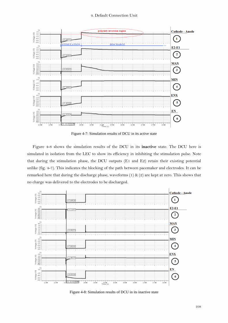
4. Default Connection Unit
108
Figure 4-7: Simulation results of DCU in its active state
Figure 4-8 shows the simulation results of the DCU in its inactive state. The DCU here is
simulated in isolation from the LEC to show its efficiency in inhibiting the stimulation pulse. Note
that during the stimulation phase, the DCU outputs (E1 and E2) retain their existing potential
unlike (fig. 4-7). This indicates the blocking of the path between pacemaker and electrodes. It can be
remarked here that during the discharge phase, waveforms (1) & (2) are kept at zero. This shows that
no charge was delivered to the electrodes to be discharged.
Figure 4-8: Simulation results of DCU in its inactive state
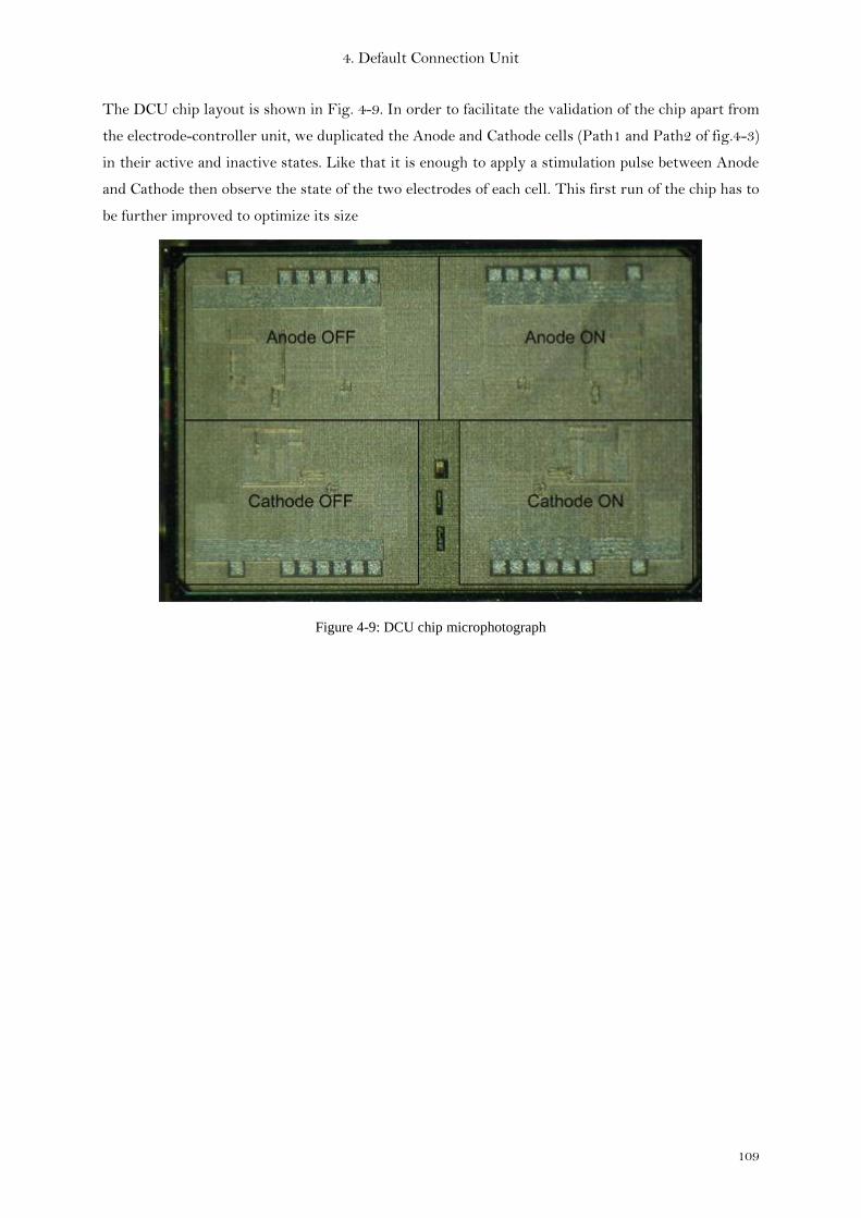
4. Default Connection Unit
109
The DCU chip layout is shown in Fig. 4-9. In order to facilitate the validation of the chip apart from
the electrode-controller unit, we duplicated the Anode and Cathode cells (Path1 and Path2 of fig.4-3)
in their active and inactive states. Like that it is enough to apply a stimulation pulse between Anode
and Cathode then observe the state of the two electrodes of each cell. This first run of the chip has to
be further improved to optimize its size
Figure 4-9: DCU chip microphotograph
4. Default Connection Unit
110
4.6 Conclusion
In this chapter we addressed the problem of multi-electrode lead compatibility with any pacemaker
device in the market. The presented DCU (Default Connection Unit) alleviates this challenge by
transforming the multi-electrode lead into a standard bipolar lead through the activation of two
electrodes that it shares their control with the main switching unit found in the electrode-controller
chip.
We showed how the DCU was designed to use the available stimulation energy to activate its paths
between Anode, Cathode and default electrodes without the need for a power source (battery). It also
stores a part of this energy in order to retain its state for a period that at least covers the discharge
phase duration. DCU paths are equipped with resistances that enable it to continue ensuring the
connection between electrodes and the pacemaker during the duration of the sensing phase which
depends on each patient.
DCU distinguishes our multi-electrode system and takes a step forward compared to the auxiliary
switching unit presented in section 3.4.3.6 of chapter 3 as it is integrated in the technology process
used in the electrode-controller chip.
As the DCU is assigned to only two electrodes in the multi-electrode lead, this may show some
limitations to the site of stimulation for the new pacemaker connected to the lead. In chapter 5 we
will introduce a new solution to address this issue. We will show how nonvolatile memories and its
underlying implementation technologies offer us ways to maintain the last configured stimulation
site and thereby allowing us to circumvent the fixed site limitation imposed by the DCU.
4. Default Connection Unit
111
Publications
I. Seoudi, J-F. Debroux, M. Laflutte, A. Makdissi, K. Amara, A. Amara, R. Dal Molin “Default
connection in multi-electrode leads for cardiac pacemakers” accepted in NEWCAS 17-20 June 2012
References
[1] Islam Seoudi et al. “Multi-electrode system for pacemaker applications”, ICECS 2011
[2] Samuel J Asirvatham “Implanting a left ventricular pacemaker lead” Indian Heart J. 2007
Mar-Apr; 59(2):197-204.
[3] A. F. Schwarz, “Computer aided design of microelectronic circuits and systems”, Academic
Press, 1987.
[4] Mark W. Kroll, Micheal H. Lehmann “Implantable cardioverter defibrillator therapy”
Springer 1996

4. Default Connection Unit
112
Enhanced Multi-Electrode Lead Using Non-Volatile Memory Technologies
113
5 Chapter 5
Enhanced Multi-Electrode Lead Using
Non-Volatile Memory Technologies

Enhanced Multi-Electrode Lead Using Non-Volatile Memory Technologies
114
Enhanced Multi-Electrode Lead Using Non-Volatile Memory Technologies
115
5.1 Introduction
In chapter 3 we presented a multi-electrode system capable of multisite stimulation. We also
presented the design challenges and constraints of such a system. In chapter 4 we furthered our
contribution by adding to the multi-electrode lead a default connection unit (DCU) which enables
compatibility of a multi-electrode lead with any other pacemaker not specifically designed to control
it. However while the DCU solution does solve the compatibility problem, as we discussed at length
in chapter 4, it does so by somewhat restricting the lead i.e. by transforming the multi-electrode lead
to standard bipolar lead. This approach, in effect not only reduces the inherent functional advantage
of a multi-electrode lead (by transforming it to a two electrode lead), but it also limits the therapeutic
advantage of such a solution. In a multi-electrode system the physician would have chosen the ideal
site/polarity of the electrodes for pacing thereby enhancing the effectiveness of the therapy, but in
the “DCU active” version of such a lead, such therapeutic advantages cannot be availed.
In this chapter, we build on the experience gained to address these limitations. We will explore the
technologies which can improve the multi-electrode lead such that the lead not only retains all the
functional features of lead as discussed in chapter 3 but enhances it by drastically bringing down the
power consumption and size. Additionally, the solution presented will also allow the lead to
incorporate within itself the DCU functionality, thus ensuring the absence of any compatibility issues
should the need of any pacemaker replacement arises. To do so we will leverage new technologies
which go beyond frontiers of standard CMOS and CMOS processes. We now discuss the key ideas
underlying the improvements to the multi-electrode lead.
5.2 Enhancements to the Multi-Electrode
In section 3.2 and 3.3 when we discussed the requirements of multi-electrode solution, we remarked
that size and power consumption are the key issues governing the design choices. The importance of
power consumption is two-fold, firstly the solution has to consume extremely low power(because
pacemakers run on batteries for several years), secondly since the LEC has to reside inside the lead,
the space restrictions rule out any onboard battery, therefore the LEC has to effectively operate on
power supplied by the pacemaker. The solution presented in Chapter 3 was based on this approach,
where before each stimulation, the pacemaker would send the power pulses to the LEC and also
configure the LEC for multi-site stimulation. This solution therefore needed configuration each
pacing cycle (therefore also power). Furthermore the time spent in configuration added to the delay
between the stimulation demand and stimulation delivery. Note that the need for configuration
stems from the fact that after the stimulation and discharge, the electrode configuration is lost and
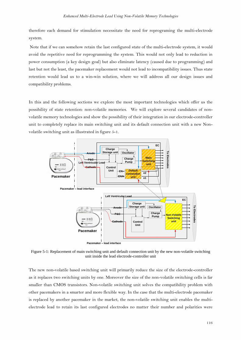
Enhanced Multi-Electrode Lead Using Non-Volatile Memory Technologies
116
therefore each demand for stimulation necessitate the need for reprograming the multi-electrode
system.
Note that if we can somehow retain the last configured state of the multi-electrode system, it would
avoid the repetitive need for reprogramming the system. This would not only lead to reduction in
power consumption (a key design goal) but also eliminate latency (caused due to programming) and
last but not the least, the pacemaker replacement would not lead to incompatibility issues. Thus state
retention would lead us to a win-win solution, where we will address all our design issues and
compatibility problems.
In this and the following sections we explore the most important technologies which offer us the
possibility of state retention: non-volatile memories. We will explore several candidates of non-
volatile memory technologies and show the possibility of their integration in our electrode-controller
unit to completely replace its main switching unit and its default connection unit with a new Non-
volatile switching unit as illustrated in figure 5-1.
Pacemaker
Pacemaker – lead interface
Left Ventricular Lead
To
Ele
ctro
de
s
EN
ENX
Main
Switching
unit
Default
connection
unit
Anode
P&C
Cathode
Charge
Storage unit
Control
Unit
Oscillator
Charge
Pump
EC
e1
e2
Pacemaker
Pacemaker – lead interface
Left Ventricular Lead
To
Ele
ctro
de
s
Non-Volatile
Switching
unit
Anode
P&C
Cathode
Charge
Storage unit
Control
Unit
Oscillator
Charge
Pump
EC
Figure 5-1: Replacement of main switching unit and default connection unit by the new non-volatile switching
unit inside the lead electrode-controller unit
The new non-volatile based switching unit will primarily reduce the size of the electrode-controller
as it replaces two switching units by one. Moreover the size of the non-volatile switching cells is far
smaller than CMOS transistors. Non-volatile switching unit solves the compatibility problem with
other pacemakers in a smarter and more flexible way. In the case that the multi-electrode pacemaker
is replaced by another pacemaker in the market, the non-volatile switching unit enables the multi-
electrode lead to retain its last configured electrodes no matter their number and polarities were
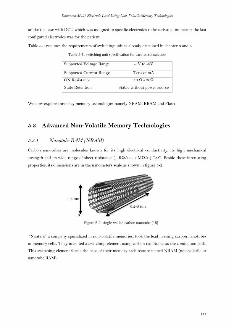
Enhanced Multi-Electrode Lead Using Non-Volatile Memory Technologies
117
unlike the case with DCU which was assigned to specific electrodes to be activated no matter the last
configured electrodes was for the patient.
Table 5-1 resumes the requirements of switching unit as already discussed in chapter 3 and 4.
Table 5-1: switching unit specification for cardiac stimulation
Supported Voltage Range -1V to -8V
Supported Current Range Tens of mA
ON Resistance 10 Ω - 20Ω
State Retention Stable without power source
We now explore three key memory technologies namely NRAM, RRAM and Flash
5.3 Advanced Non-Volatile Memory Technologies
5.3.1 Nanotube RAM (NRAM)
Carbon nanotubes are molecules known for its high electrical conductivity, its high mechanical
strength and its wide range of sheet resistance (1 KΩ/ - 1 MΩ/) [22]. Beside these interesting
properties, its dimensions are in the nanometers scale as shown in figure 5-2.
6
Figure 5-2: single walled carbon nanotube [18]
“Nantero” a company specialized in non-volatile memories, took the lead in using carbon nanotubes
in memory cells. They invented a switching element using carbon nanotubes as the conduction path.
This switching element forms the base of their memory architecture named NRAM (non-volatile or
nanotube RAM).
1-2 nm
0.2-5 µm
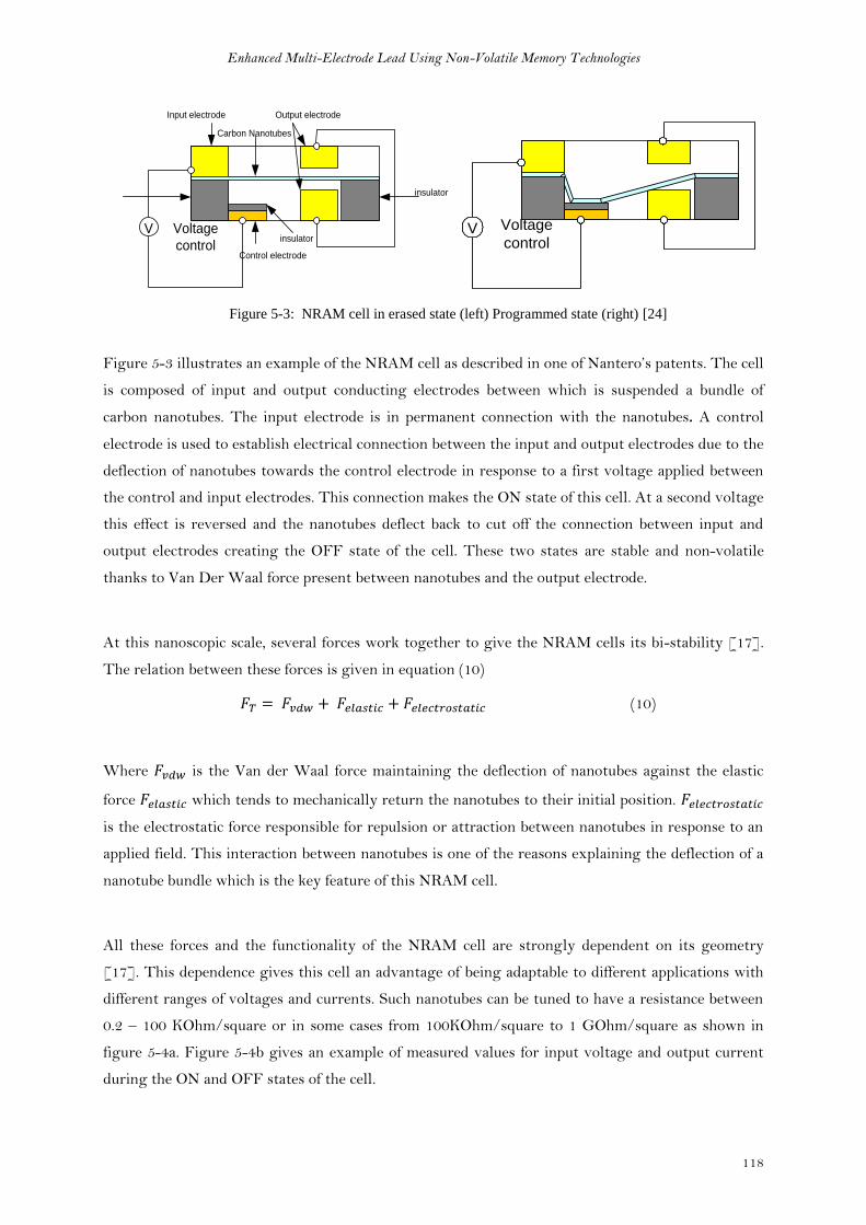
Enhanced Multi-Electrode Lead Using Non-Volatile Memory Technologies
118
Voltage
control
Input electrode Output electrode
insulator
insulator
Control electrode
V
Carbon Nanotubes
Voltage
controlV
Figure 5-3: NRAM cell in erased state (left) Programmed state (right) [24]
Figure 5-3 illustrates an example of the NRAM cell as described in one of Nantero’s patents. The cell
is composed of input and output conducting electrodes between which is suspended a bundle of
carbon nanotubes. The input electrode is in permanent connection with the nanotubes. A control
electrode is used to establish electrical connection between the input and output electrodes due to the
deflection of nanotubes towards the control electrode in response to a first voltage applied between
the control and input electrodes. This connection makes the ON state of this cell. At a second voltage
this effect is reversed and the nanotubes deflect back to cut off the connection between input and
output electrodes creating the OFF state of the cell. These two states are stable and non-volatile
thanks to Van Der Waal force present between nanotubes and the output electrode.
At this nanoscopic scale, several forces work together to give the NRAM cells its bi-stability [17].
The relation between these forces is given in equation (10)
(10)
Where is the Van der Waal force maintaining the deflection of nanotubes against the elastic
force which tends to mechanically return the nanotubes to their initial position.
is the electrostatic force responsible for repulsion or attraction between nanotubes in response to an
applied field. This interaction between nanotubes is one of the reasons explaining the deflection of a
nanotube bundle which is the key feature of this NRAM cell.
All these forces and the functionality of the NRAM cell are strongly dependent on its geometry
[17]. This dependence gives this cell an advantage of being adaptable to different applications with
different ranges of voltages and currents. Such nanotubes can be tuned to have a resistance between
0.2 – 100 KOhm/square or in some cases from 100KOhm/square to 1 GOhm/square as shown in
figure 5-4a. Figure 5-4b gives an example of measured values for input voltage and output current
during the ON and OFF states of the cell.
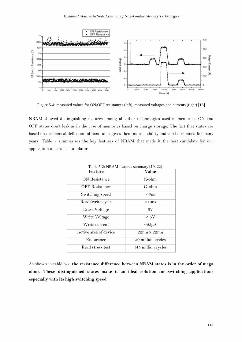
Enhanced Multi-Electrode Lead Using Non-Volatile Memory Technologies
119
Figure 5-4: measured values for ON/OFF resistances (left), measured voltages and currents (right) [16]
NRAM showed distinguishing features among all other technologies used in memories. ON and
OFF states don’t leak as in the case of memories based on charge storage. The fact that states are
based on mechanical deflection of nanotubes gives them more stability and can be retained for many
years. Table 8 summarises the key features of NRAM that made it the best candidate for our
application in cardiac stimulators.
Table 5-2: NRAM features summary [19, 22]
Feature Value
ON Resistance K-ohm
OFF Resistance G-ohm
Switching speed <3ns
Read/write cycle <10ns
Erase Voltage 6V
Write Voltage < 5V
Write current ~25µA
Active area of device 22nm x 22nm
Endurance 50 million cycles
Read stress test 145 million cycles
As shown in table 5-2, the resistance difference between NRAM states is in the order of mega
ohms. These distinguished states make it an ideal solution for switching applications
especially with its high switching speed.
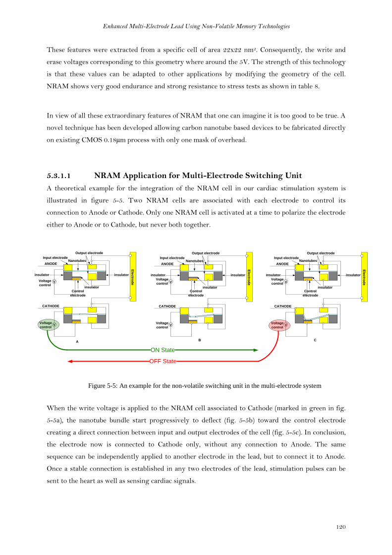
Enhanced Multi-Electrode Lead Using Non-Volatile Memory Technologies
120
These features were extracted from a specific cell of area 22x22 nm2. Consequently, the write and
erase voltages corresponding to this geometry where around the 5V. The strength of this technology
is that these values can be adapted to other applications by modifying the geometry of the cell.
NRAM shows very good endurance and strong resistance to stress tests as shown in table 8.
In view of all these extraordinary features of NRAM that one can imagine it is too good to be true. A
novel technique has been developed allowing carbon nanotube based devices to be fabricated directly
on existing CMOS 0.18µm process with only one mask of overhead.
5.3.1.1 NRAM Application for Multi-Electrode Switching Unit
A theoretical example for the integration of the NRAM cell in our cardiac stimulation system is
illustrated in figure 5-5. Two NRAM cells are associated with each electrode to control its
connection to Anode or Cathode. Only one NRAM cell is activated at a time to polarize the electrode
either to Anode or to Cathode, but never both together.
OFF State
ANODE
CATHODE
Input electrodeNanotubes
Output electrode
insulatorinsulator
insulatorControl
electrode
V
VVoltage
control
Voltage
control
Ele
ctro
de
ANODE
CATHODE
Input electrodeNanotubes
Output electrode
insulatorinsulator
insulatorControl
electrode
V
VVoltage
control
Voltage
control
Ele
ctro
de
ANODE
CATHODE
Input electrodeNanotubes
Output electrode
insulatorinsulator
insulatorControl
electrode
V
VVoltage
control
Voltage
control
Ele
ctro
de
ON State
A B C
Figure 5-5: An example for the non-volatile switching unit in the multi-electrode system
When the write voltage is applied to the NRAM cell associated to Cathode (marked in green in fig.
5-5a), the nanotube bundle start progressively to deflect (fig. 5-5b) toward the control electrode
creating a direct connection between input and output electrodes of the cell (fig. 5-5c). In conclusion,
the electrode now is connected to Cathode only, without any connection to Anode. The same
sequence can be independently applied to another electrode in the lead, but to connect it to Anode.
Once a stable connection is established in any two electrodes of the lead, stimulation pulses can be
sent to the heart as well as sensing cardiac signals.

Enhanced Multi-Electrode Lead Using Non-Volatile Memory Technologies
121
By applying the erase voltage to the NRAM cell as marked in red in figure 5-5c, the nanotube bundle
deflect back to its initial position cutting off the connection between input and output electrodes.
The stability of NRAM states and its immunity against bit failure caused by charge leakage,
magnetic field or even alpha particles makes it very reliable technology specially in medical
applications. Adding to that its miniaturized size and its speed switching makes it the best
technology to be adopted for our application.
But the existing NRAM cells with their actual targeted applications in the non-volatile memory
applications, are not adapted to our specifications which requires the support of important amount of
currents (tens milliamps) and voltages (tens of Volts) during the stimulation phase. We investigated
with the technology inventor (Nantero) the feasibility of enhancing the cell features in order to
match our system’s specification. They confirmed the feasibility but it would require further research
and studies to be invested in this direction in future.
One intermediate solution for the existing NRAM cells (without geometrical modification) to
support stimulation currents in our system could be achieved by employing several NRAM cells
mounted parallel to each other. By that the stimulation current is divided into the parallel cells
preserving each of them from being damaged.
At this point, our goal was to prove the concept which is more or less theoretically reached. We
decided to take a further step and to try another technology in the non-volatile memory field. In the
next section we will explore two technologies (MRAM and Memristance) that we believe they can be
grouped under the same family of resistive RAM as will be revealed later in this chapter.
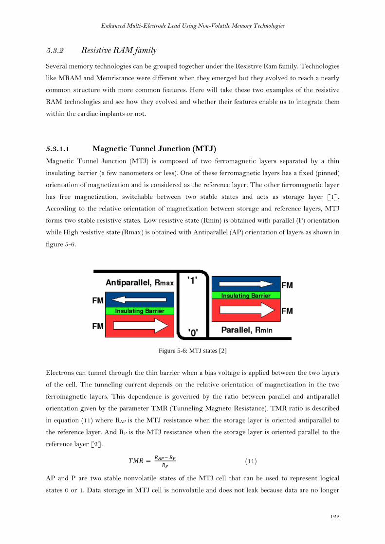
Enhanced Multi-Electrode Lead Using Non-Volatile Memory Technologies
122
5.3.2 Resistive RAM family
Several memory technologies can be grouped together under the Resistive Ram family. Technologies
like MRAM and Memristance were different when they emerged but they evolved to reach a nearly
common structure with more common features. Here will take these two examples of the resistive
RAM technologies and see how they evolved and whether their features enable us to integrate them
within the cardiac implants or not.
5.3.1.1 Magnetic Tunnel Junction (MTJ)
Magnetic Tunnel Junction (MTJ) is composed of two ferromagnetic layers separated by a thin
insulating barrier (a few nanometers or less). One of these ferromagnetic layers has a fixed (pinned)
orientation of magnetization and is considered as the reference layer. The other ferromagnetic layer
has free magnetization, switchable between two stable states and acts as storage layer [1].
According to the relative orientation of magnetization between storage and reference layers, MTJ
forms two stable resistive states. Low resistive state (Rmin) is obtained with parallel (P) orientation
while High resistive state (Rmax) is obtained with Antiparallel (AP) orientation of layers as shown in
figure 5-6.
Figure 5-6: MTJ states [2]
Electrons can tunnel through the thin barrier when a bias voltage is applied between the two layers
of the cell. The tunneling current depends on the relative orientation of magnetization in the two
ferromagnetic layers. This dependence is governed by the ratio between parallel and antiparallel
orientation given by the parameter TMR (Tunneling Magneto Resistance). TMR ratio is described
in equation (11) where RAP is the MTJ resistance when the storage layer is oriented antiparallel to
the reference layer. And RP is the MTJ resistance when the storage layer is oriented parallel to the
reference layer [2].
(11)
AP and P are two stable nonvolatile states of the MTJ cell that can be used to represent logical
states 0 or 1. Data storage in MTJ cell is nonvolatile and does not leak because data are no longer
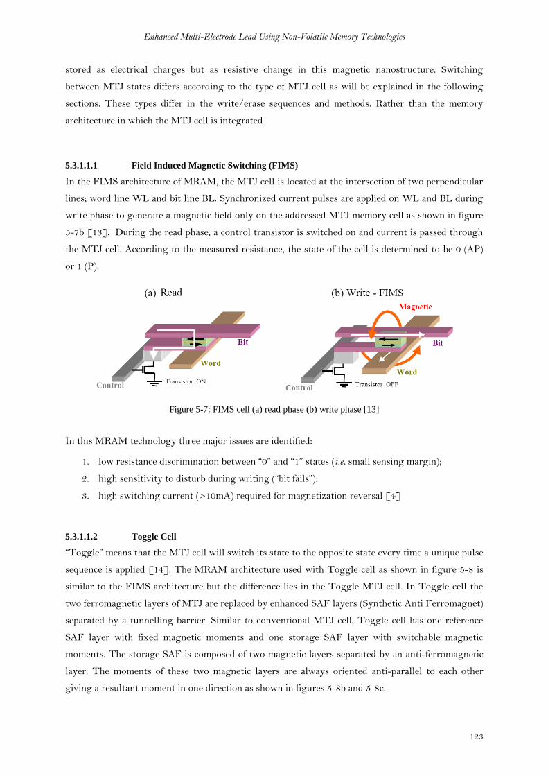
Enhanced Multi-Electrode Lead Using Non-Volatile Memory Technologies
123
stored as electrical charges but as resistive change in this magnetic nanostructure. Switching
between MTJ states differs according to the type of MTJ cell as will be explained in the following
sections. These types differ in the write/erase sequences and methods. Rather than the memory
architecture in which the MTJ cell is integrated
5.3.1.1.1 Field Induced Magnetic Switching (FIMS)
In the FIMS architecture of MRAM, the MTJ cell is located at the intersection of two perpendicular
lines; word line WL and bit line BL. Synchronized current pulses are applied on WL and BL during
write phase to generate a magnetic field only on the addressed MTJ memory cell as shown in figure
5-7b [13]. During the read phase, a control transistor is switched on and current is passed through
the MTJ cell. According to the measured resistance, the state of the cell is determined to be 0 (AP)
or 1 (P).
Figure 5-7: FIMS cell (a) read phase (b) write phase [13]
In this MRAM technology three major issues are identified:
1. low resistance discrimination between “0” and “1” states (i.e. small sensing margin);
2. high sensitivity to disturb during writing (“bit fails”);
3. high switching current (>10mA) required for magnetization reversal [4]
5.3.1.1.2 Toggle Cell
“Toggle” means that the MTJ cell will switch its state to the opposite state every time a unique pulse
sequence is applied [14]. The MRAM architecture used with Toggle cell as shown in figure 5-8 is
similar to the FIMS architecture but the difference lies in the Toggle MTJ cell. In Toggle cell the
two ferromagnetic layers of MTJ are replaced by enhanced SAF layers (Synthetic Anti Ferromagnet)
separated by a tunnelling barrier. Similar to conventional MTJ cell, Toggle cell has one reference
SAF layer with fixed magnetic moments and one storage SAF layer with switchable magnetic
moments. The storage SAF is composed of two magnetic layers separated by an anti-ferromagnetic
layer. The moments of these two magnetic layers are always oriented anti-parallel to each other
giving a resultant moment in one direction as shown in figures 5-8b and 5-8c.
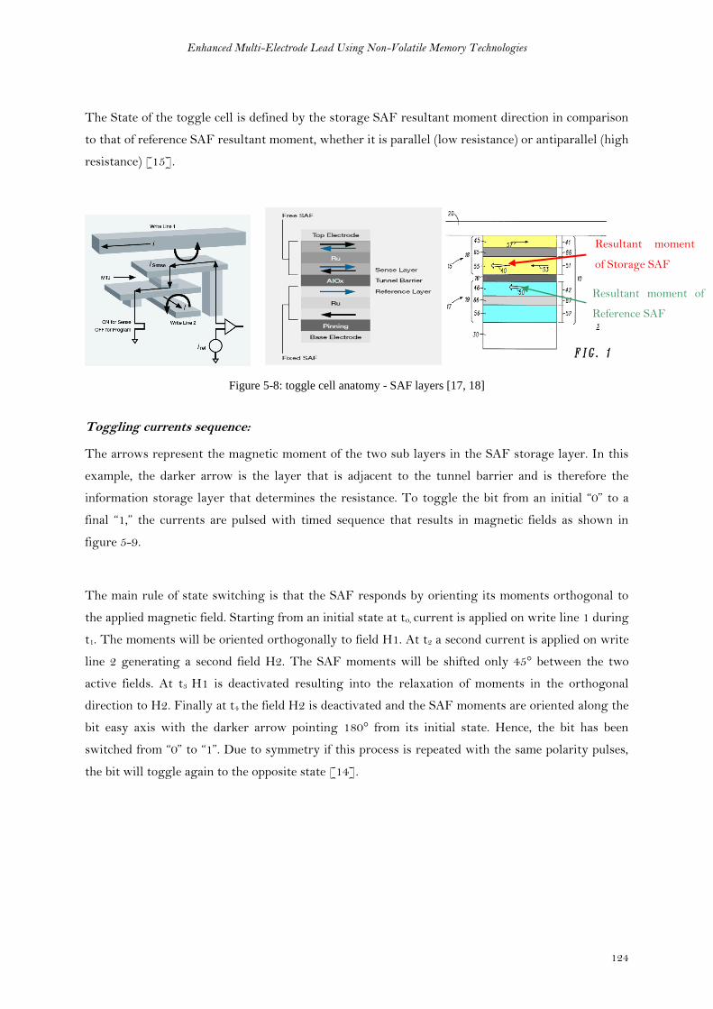
Enhanced Multi-Electrode Lead Using Non-Volatile Memory Technologies
124
The State of the toggle cell is defined by the storage SAF resultant moment direction in comparison
to that of reference SAF resultant moment, whether it is parallel (low resistance) or antiparallel (high
resistance) [15].
Figure 5-8: toggle cell anatomy - SAF layers [17, 18]
Toggling currents sequence:
The arrows represent the magnetic moment of the two sub layers in the SAF storage layer. In this
example, the darker arrow is the layer that is adjacent to the tunnel barrier and is therefore the
information storage layer that determines the resistance. To toggle the bit from an initial “0” to a
final “1,” the currents are pulsed with timed sequence that results in magnetic fields as shown in
figure 5-9.
The main rule of state switching is that the SAF responds by orienting its moments orthogonal to
the applied magnetic field. Starting from an initial state at to, current is applied on write line 1 during
t1. The moments will be oriented orthogonally to field H1. At t2 a second current is applied on write
line 2 generating a second field H2. The SAF moments will be shifted only 45° between the two
active fields. At t3 H1 is deactivated resulting into the relaxation of moments in the orthogonal
direction to H2. Finally at t4 the field H2 is deactivated and the SAF moments are oriented along the
bit easy axis with the darker arrow pointing 180° from its initial state. Hence, the bit has been
switched from “0” to “1”. Due to symmetry if this process is repeated with the same polarity pulses,
the bit will toggle again to the opposite state [14].
Resultant moment
of Storage SAF
Resultant moment of
Reference SAF
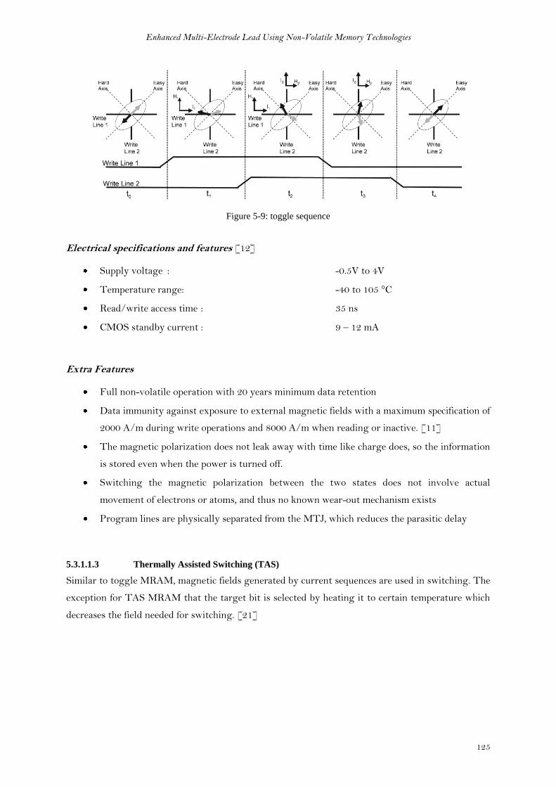
Enhanced Multi-Electrode Lead Using Non-Volatile Memory Technologies
125
Figure 5-9: toggle sequence
Electrical specifications and features [12]
Supply voltage : -0.5V to 4V
Temperature range: -40 to 105 °C
Read/write access time : 35 ns
CMOS standby current : 9 – 12 mA
Extra Features
Full non-volatile operation with 20 years minimum data retention
Data immunity against exposure to external magnetic fields with a maximum specification of
2000 A/m during write operations and 8000 A/m when reading or inactive. [11]
The magnetic polarization does not leak away with time like charge does, so the information
is stored even when the power is turned off.
Switching the magnetic polarization between the two states does not involve actual
movement of electrons or atoms, and thus no known wear-out mechanism exists
Program lines are physically separated from the MTJ, which reduces the parasitic delay
5.3.1.1.3 Thermally Assisted Switching (TAS)
Similar to toggle MRAM, magnetic fields generated by current sequences are used in switching. The
exception for TAS MRAM that the target bit is selected by heating it to certain temperature which
decreases the field needed for switching. [21]
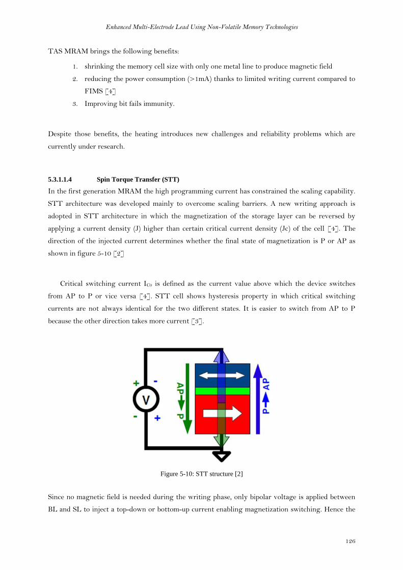
Enhanced Multi-Electrode Lead Using Non-Volatile Memory Technologies
126
TAS MRAM brings the following benefits:
1. shrinking the memory cell size with only one metal line to produce magnetic field
2. reducing the power consumption (>1mA) thanks to limited writing current compared to
FIMS [4]
3. Improving bit fails immunity.
Despite those benefits, the heating introduces new challenges and reliability problems which are
currently under research.
5.3.1.1.4 Spin Torque Transfer (STT)
In the first generation MRAM the high programming current has constrained the scaling capability.
STT architecture was developed mainly to overcome scaling barriers. A new writing approach is
adopted in STT architecture in which the magnetization of the storage layer can be reversed by
applying a current density (J) higher than certain critical current density (Jc) of the cell [4]. The
direction of the injected current determines whether the final state of magnetization is P or AP as
shown in figure 5-10 [2]
Critical switching current IC0 is defined as the current value above which the device switches
from AP to P or vice versa [4]. STT cell shows hysteresis property in which critical switching
currents are not always identical for the two different states. It is easier to switch from AP to P
because the other direction takes more current [3].
Figure 5-10: STT structure [2]
Since no magnetic field is needed during the writing phase, only bipolar voltage is applied between
BL and SL to inject a top-down or bottom-up current enabling magnetization switching. Hence the
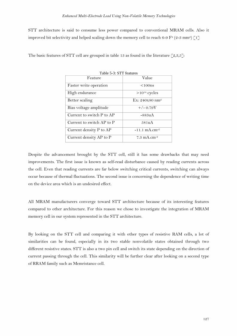
Enhanced Multi-Electrode Lead Using Non-Volatile Memory Technologies
127
STT architecture is said to consume less power compared to conventional MRAM cells. Also it
improved bit selectivity and helped scaling down the memory cell to reach 6-9 F2 (2-3 mm2) [1]
The basic features of STT cell are grouped in table 13 as found in the literature [2,3,5]:
Table 5-3: STT features
Feature Value
Faster write operation <100ns
High endurance >1014 cycles
Better scaling Ex: 240x80 nm2
Bias voltage amplitude +/- 0.79V
Current to switch P to AP -883uA
Current to switch AP to P 581uA
Current density P to AP -11.1 mA.cm-2
Current density AP to P 7.3 mA.cm-2
Despite the advancement brought by the STT cell, still it has some drawbacks that may need
improvements. The first issue is known as self-read disturbance caused by reading currents across
the cell. Even that reading currents are far below switching critical currents, switching can always
occur because of thermal fluctuations. The second issue is concerning the dependence of writing time
on the device area which is an undesired effect.
All MRAM manufacturers converge toward STT architecture because of its interesting features
compared to other architecture. For this reason we chose to investigate the integration of MRAM
memory cell in our system represented in the STT architecture.
By looking on the STT cell and comparing it with other types of resistive RAM cells, a lot of
similarities can be found, especially in its two stable nonvolatile states obtained through two
different resistive states. STT is also a two pin cell and switch its state depending on the direction of
current passing through the cell. This similarity will be further clear after looking on a second type
of RRAM family such as Memristance cell.

Enhanced Multi-Electrode Lead Using Non-Volatile Memory Technologies
128
5.3.1.2 Memristance
Memristance is a shorter name of memory resistor given by Leon Chua in 1971 to be the 4th
fundamental circuit element that defines a relation between flux and charge. Chua proved
theoretically this relationship through symmetry of relationships describing each of the three
fundamental circuit elements [5].
Therefore the Memristance completes the symmetry and define the missing relationship between
flux and charge
In 2008 researchers from HP lab built a nanoscale Memristor switch – 50nmx50nm – by
sandwiching a semiconductor material (Titanium oxide) of thickness D between two nanowires as
shown in figure 5-11. As charge q is the time integral of current, and flux is the time integral of
voltage according to faraday’s law, therefore the memristance (M(q))can be modelled in terms of
nonlinear resistance. The total resistance of the device is determined by two variable resistors
connected in series. The doped region of the semiconductor represents a low resistance RON while
the undoped region of the semiconductor represents a high resistance ROFF. The barrier between
these two regions moves in the same direction as electric current generated by the applied bias
voltage across the device [6]. The barrier position is presented by the state variable w that varies
between 0 (undoped ROFF state) and full length D (doped RON state).
Figure 5-11: Memristance model
The characteristic equation of the memristance model is given by equation (12)
(12)
And the state variable is given by
(13)
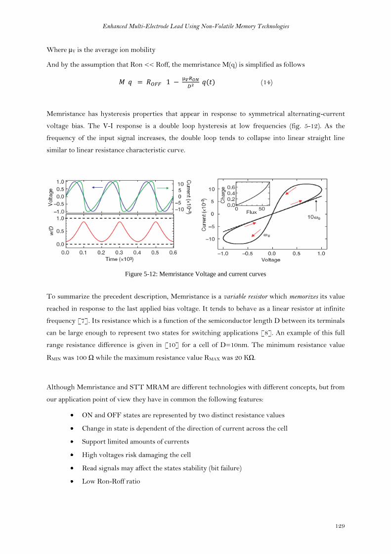
Enhanced Multi-Electrode Lead Using Non-Volatile Memory Technologies
129
Where µV is the average ion mobility
And by the assumption that Ron << Roff, the memristance M(q) is simplified as follows
(14)
Memristance has hysteresis properties that appear in response to symmetrical alternating-current
voltage bias. The V-I response is a double loop hysteresis at low frequencies (fig. 5-12). As the
frequency of the input signal increases, the double loop tends to collapse into linear straight line
similar to linear resistance characteristic curve.
Figure 5-12: Memristance Voltage and current curves
To summarize the precedent description, Memristance is a variable resistor which memorizes its value
reached in response to the last applied bias voltage. It tends to behave as a linear resistor at infinite
frequency [7]. Its resistance which is a function of the semiconductor length D between its terminals
can be large enough to represent two states for switching applications [8]. An example of this full
range resistance difference is given in [10] for a cell of D=10nm. The minimum resistance value
RMIN was 100 Ω while the maximum resistance value RMAX was 20 KΩ.
Although Memristance and STT MRAM are different technologies with different concepts, but from
our application point of view they have in common the following features:
ON and OFF states are represented by two distinct resistance values
Change in state is dependent of the direction of current across the cell
Support limited amounts of currents
High voltages risk damaging the cell
Read signals may affect the states stability (bit failure)
Low Ron-Roff ratio
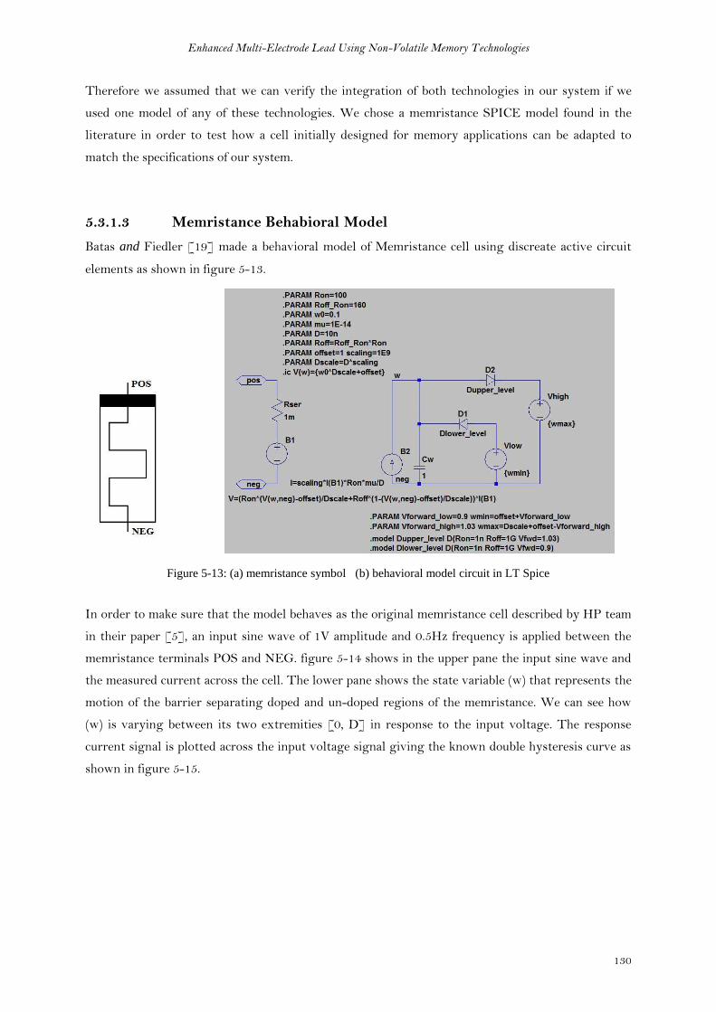
Enhanced Multi-Electrode Lead Using Non-Volatile Memory Technologies
130
Therefore we assumed that we can verify the integration of both technologies in our system if we
used one model of any of these technologies. We chose a memristance SPICE model found in the
literature in order to test how a cell initially designed for memory applications can be adapted to
match the specifications of our system.
5.3.1.3 Memristance Behabioral Model
Batas and Fiedler [19] made a behavioral model of Memristance cell using discreate active circuit
elements as shown in figure 5-13.
Figure 5-13: (a) memristance symbol (b) behavioral model circuit in LT Spice
In order to make sure that the model behaves as the original memristance cell described by HP team
in their paper [5], an input sine wave of 1V amplitude and 0.5Hz frequency is applied between the
memristance terminals POS and NEG. figure 5-14 shows in the upper pane the input sine wave and
the measured current across the cell. The lower pane shows the state variable (w) that represents the
motion of the barrier separating doped and un-doped regions of the memristance. We can see how
(w) is varying between its two extremities [0, D] in response to the input voltage. The response
current signal is plotted across the input voltage signal giving the known double hysteresis curve as
shown in figure 5-15.
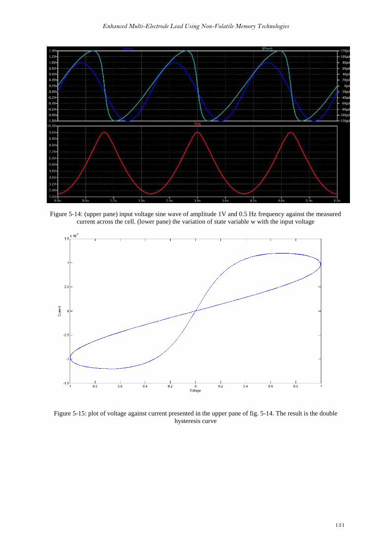
Enhanced Multi-Electrode Lead Using Non-Volatile Memory Technologies
131
Figure 5-14: (upper pane) input voltage sine wave of amplitude 1V and 0.5 Hz frequency against the measured
current across the cell. (lower pane) the variation of state variable w with the input voltage
Figure 5-15: plot of voltage against current presented in the upper pane of fig. 5-14. The result is the double
hysteresis curve
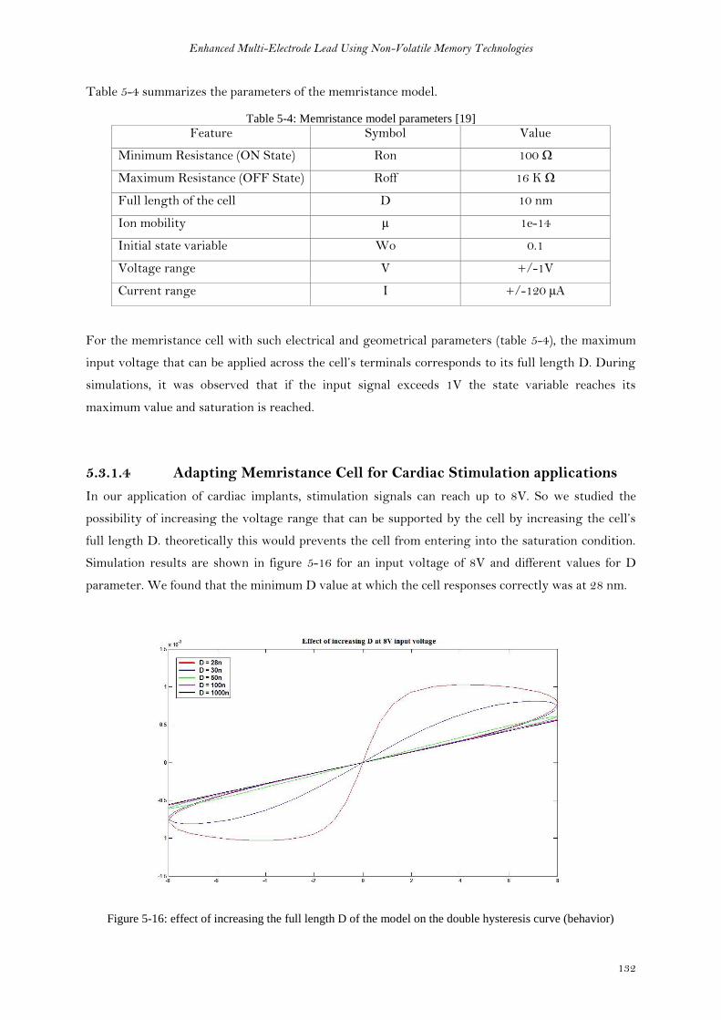
Enhanced Multi-Electrode Lead Using Non-Volatile Memory Technologies
132
Table 5-4 summarizes the parameters of the memristance model.
Table 5-4: Memristance model parameters [19]
Feature Symbol Value
Minimum Resistance (ON State) Ron 100 Ω
Maximum Resistance (OFF State) Roff 16 K Ω
Full length of the cell D 10 nm
Ion mobility µ 1e-14
Initial state variable Wo 0.1
Voltage range V +/-1V
Current range I +/-120 µA
For the memristance cell with such electrical and geometrical parameters (table 5-4), the maximum
input voltage that can be applied across the cell’s terminals corresponds to its full length D. During
simulations, it was observed that if the input signal exceeds 1V the state variable reaches its
maximum value and saturation is reached.
5.3.1.4 Adapting Memristance Cell for Cardiac Stimulation applications
In our application of cardiac implants, stimulation signals can reach up to 8V. So we studied the
possibility of increasing the voltage range that can be supported by the cell by increasing the cell’s
full length D. theoretically this would prevents the cell from entering into the saturation condition.
Simulation results are shown in figure 5-16 for an input voltage of 8V and different values for D
parameter. We found that the minimum D value at which the cell responses correctly was at 28 nm.
Figure 5-16: effect of increasing the full length D of the model on the double hysteresis curve (behavior)
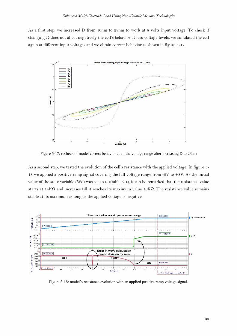
Enhanced Multi-Electrode Lead Using Non-Volatile Memory Technologies
133
As a first step, we increased D from 10nm to 28nm to work at 8 volts input voltage. To check if
changing D does not affect negatively the cell’s behavior at less voltage levels, we simulated the cell
again at different input voltages and we obtain correct behavior as shown in figure 5-17.
Figure 5-17: recheck of model correct behavior at all the voltage range after increasing D to 28nm
As a second step, we tested the evolution of the cell’s resistance with the applied voltage. In figure 5-
18 we applied a positive ramp signal covering the full voltage range from -8V to +8V. As the initial
value of the state variable (Wo) was set to 0.1(table 5-4), it can be remarked that the resistance value
starts at 14KΩ and increases till it reaches its maximum value 16KΩ. The resistance value remains
stable at its maximum as long as the applied voltage is negative.
Error in wave calculation
due to division by zero
(V/I)OFF
ON
Figure 5-18: model’s resistance evolution with an applied positive ramp voltage signal.
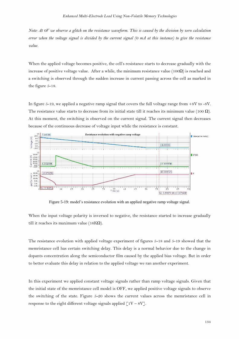
Enhanced Multi-Electrode Lead Using Non-Volatile Memory Technologies
134
Note: At 0V we observe a glitch on the resistance waveform. This is caused by the division by zero calculation
error when the voltage signal is divided by the current signal (0 mA at this instance) to give the resistance
value.
When the applied voltage becomes positive, the cell’s resistance starts to decrease gradually with the
increase of positive voltage value. After a while, the minimum resistance value (100Ω) is reached and
a switching is observed through the sudden increase in current passing across the cell as marked in
the figure 5-18.
In figure 5-19, we applied a negative ramp signal that covers the full voltage range from +8V to -8V.
The resistance value starts to decrease from its initial state till it reaches its minimum value (100 Ω).
At this moment, the switching is observed on the current signal. The current signal then decreases
because of the continuous decrease of voltage input while the resistance is constant.
Figure 5-19: model’s resistance evolution with an applied negative ramp voltage signal.
When the input voltage polarity is inversed to negative, the resistance started to increase gradually
till it reaches its maximum value (16KΩ).
The resistance evolution with applied voltage experiment of figures 5-18 and 5-19 showed that the
memristance cell has certain switching delay. This delay is a normal behavior due to the change in
dopants concentration along the semiconductor film caused by the applied bias voltage. But in order
to better evaluate this delay in relation to the applied voltage we ran another experiment.
In this experiment we applied constant voltage signals rather than ramp voltage signals. Given that
the initial state of the memristance cell model is OFF, we applied positive voltage signals to observe
the switching of the state. Figure 5-20 shows the current values across the memristance cell in
response to the eight different voltage signals applied [1V – 8V].

Enhanced Multi-Electrode Lead Using Non-Volatile Memory Technologies
135
Figure 5-20: Memristance model switching delay for different positive voltage applied across the cell
It is clear from figure 5-20 that as the voltage increases, the switching delay decreases. But the
surprise here was the very long switching delay observed. At 8V where we expected the shortest
switching delay, it was observed at 0.6 sec. while at 1V the switching delay was tremendously long
of 5 seconds.
Even that this model does not reflect precisely the physical properties of the memristance cell, the
observed switching delays during this experiment predicts certain trend for the impact of the
increase in the cell’s full length D. This amount of switching delays cannot be tolerated in
systems like cardiac stimulators and is considered as a blocking point for the integration of
this technology within the system.
Another blocking point for this technology was observed during an experiment to test the stability
of the memristance states facing conditions near to that of our application. First, the resistance value
for ON and OFF states were set to 1K and 160K respectively. As in the cardiac stimulation systems,
the stimulation signal is in the form of pulses that repeats every cardiac cycle (ex: 1 second), we
applied a series of positive pulses at 8V to pass through the memristance cell (upper pane of fig.5-21).
The cell is initially set to OFF state. Therefore we expected that the applied voltage signal would be
blocked.
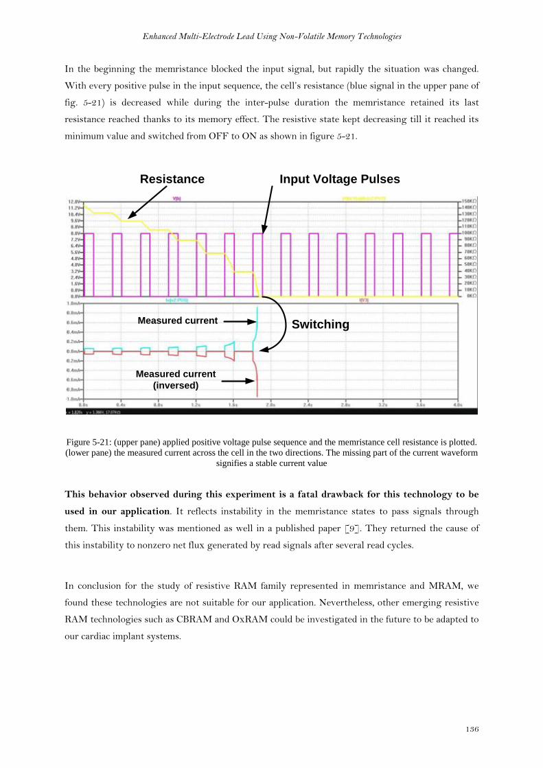
Enhanced Multi-Electrode Lead Using Non-Volatile Memory Technologies
136
In the beginning the memristance blocked the input signal, but rapidly the situation was changed.
With every positive pulse in the input sequence, the cell’s resistance (blue signal in the upper pane of
fig. 5-21) is decreased while during the inter-pulse duration the memristance retained its last
resistance reached thanks to its memory effect. The resistive state kept decreasing till it reached its
minimum value and switched from OFF to ON as shown in figure 5-21.
Resistance Input Voltage Pulses
SwitchingMeasured current
Measured current
(inversed)
Figure 5-21: (upper pane) applied positive voltage pulse sequence and the memristance cell resistance is plotted.
(lower pane) the measured current across the cell in the two directions. The missing part of the current waveform
signifies a stable current value
This behavior observed during this experiment is a fatal drawback for this technology to be
used in our application. It reflects instability in the memristance states to pass signals through
them. This instability was mentioned as well in a published paper [9]. They returned the cause of
this instability to nonzero net flux generated by read signals after several read cycles.
In conclusion for the study of resistive RAM family represented in memristance and MRAM, we
found these technologies are not suitable for our application. Nevertheless, other emerging resistive
RAM technologies such as CBRAM and OxRAM could be investigated in the future to be adapted to
our cardiac implant systems.
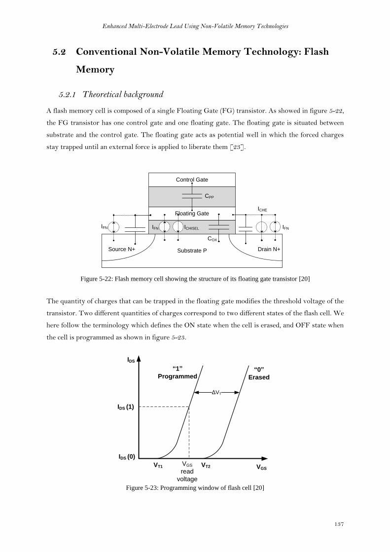
Enhanced Multi-Electrode Lead Using Non-Volatile Memory Technologies
137
5.2 Conventional Non-Volatile Memory Technology: Flash
Memory
5.2.1 Theoretical background
A flash memory cell is composed of a single Floating Gate (FG) transistor. As showed in figure 5-22,
the FG transistor has one control gate and one floating gate. The floating gate is situated between
substrate and the control gate. The floating gate acts as potential well in which the forced charges
stay trapped until an external force is applied to liberate them [23].
Control Gate
Floating Gate
Substrate P Drain N+Source N+
CPP
COX
IFN IFN
ICHE
ICHISELIFN
Figure 5-22: Flash memory cell showing the structure of its floating gate transistor [20]
The quantity of charges that can be trapped in the floating gate modifies the threshold voltage of the
transistor. Two different quantities of charges correspond to two different states of the flash cell. We
here follow the terminology which defines the ON state when the cell is erased, and OFF state when
the cell is programmed as shown in figure 5-23.
VGS
IDS
VT1 VT2
“1”
Programmed“0”
Erased
IDS (1)
IDS (0)VGS
read
voltage
ΔVT
Figure 5-23: Programming window of flash cell [20]

Enhanced Multi-Electrode Lead Using Non-Volatile Memory Technologies
138
Flash cell is programmed and erased electrically by two possible methods named Fowler Norheim
Injection and Channel Hot Electron. They are represented in figure 5-22 as current sources IFN and
ICHE respectively.
CPP is the capacitance between floating gate and control gate, COX is the Capacitance between
floating gate and substrate, CGS is the Gate-Source capacitance and CGD is the Gate–Drain
capacitance.
The behavior of the floating gate transistors are defined in the triode and saturation regions by
equations (15) and (16) respectively [23].
(15)
(16)
Where
, , and is a conductivity factor
From the previous equations, it can be deduced that the FG transistor can conduct current even
when |VGS| < |VT|. This effect is called “drain turn-on” and it occurs because the channel can be
turned on by the drain voltage due to the presence of the term in equation (16).
In order to read the state of a Flash cell, a bias voltage has to be applied between the control gate
and source. The value of this bias voltage has to be in the middle way between the two threshold
voltages of the flash cell (figure 5-23). Drain voltage has to be maintained at around 1V.
Table 5-5 shows an example of bias voltages applied on Source, Control Gate and Drain of a typical
flash cell during the different operations. The substrate is generally grounded, but by applying
negative voltage of -2V can reduce the consumption
Table 5-5: typical bias voltages for flash cell [23]
Source Control Gate Drain
Read GND 5V 1V
Program GND 12V 5-7 V
Erase 12V GND Floating

Enhanced Multi-Electrode Lead Using Non-Volatile Memory Technologies
139
5.2.2 Flash cell model
In terms of research collaboration between ISEP and IM2NP lab of Marseille we used their compact
model of flash cell [20] in order to validate the concept of its integration in the cardiac stimulation
system. The model is built on PSP MOS model of N-type and gate dimensions: W= 90nm, L=180nm
and tox=9.8nm. Program and erase mechanisms are performed by Fownler Nordheim (FN) and Hot
Channel Electron (CHE).
The model of Flash memory cell is presented in figure 5-22 with its three principal components:
MOS transistor to describe the channel behavior
Capacitances to isolate the floating gate node
Current sources to model injection currents
Starting from the VerilogA files of the flash model, we generated a symbol using Mentor Graphics
environment in order to facilitate the simulation of the model with our system in Eldo.
In order to verify that our generated cell behavior corresponds to the model behavior, we simulated
the Program/Erase sequences on the Flash symbol generated in Mentor Graphics environment.
5.2.2.1 Program Sequence using Channel Hot Electron Method
The flash cell has four functional I/O terminals representing Bulk (B), Source (S), G (Control Gate)
and Drain (D). It has another three outputs used to observe the change in threshold voltage (VT),
Floating gate voltage (FG) and the injection currents (IG).
Figure 5-24: symbol for the generated flash cell - Program sequence
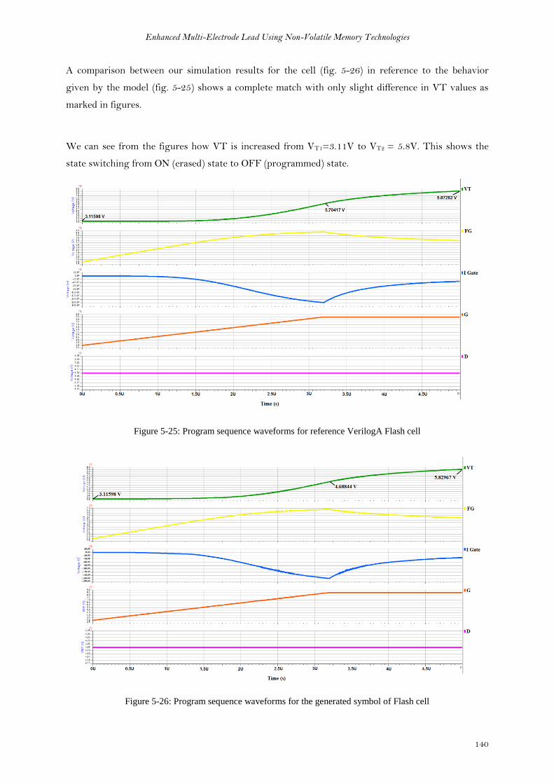
Enhanced Multi-Electrode Lead Using Non-Volatile Memory Technologies
140
A comparison between our simulation results for the cell (fig. 5-26) in reference to the behavior
given by the model (fig. 5-25) shows a complete match with only slight difference in VT values as
marked in figures.
We can see from the figures how VT is increased from VT1=3.11V to VT2 = 5.8V. This shows the
state switching from ON (erased) state to OFF (programmed) state.
Figure 5-25: Program sequence waveforms for reference VerilogA Flash cell
Figure 5-26: Program sequence waveforms for the generated symbol of Flash cell
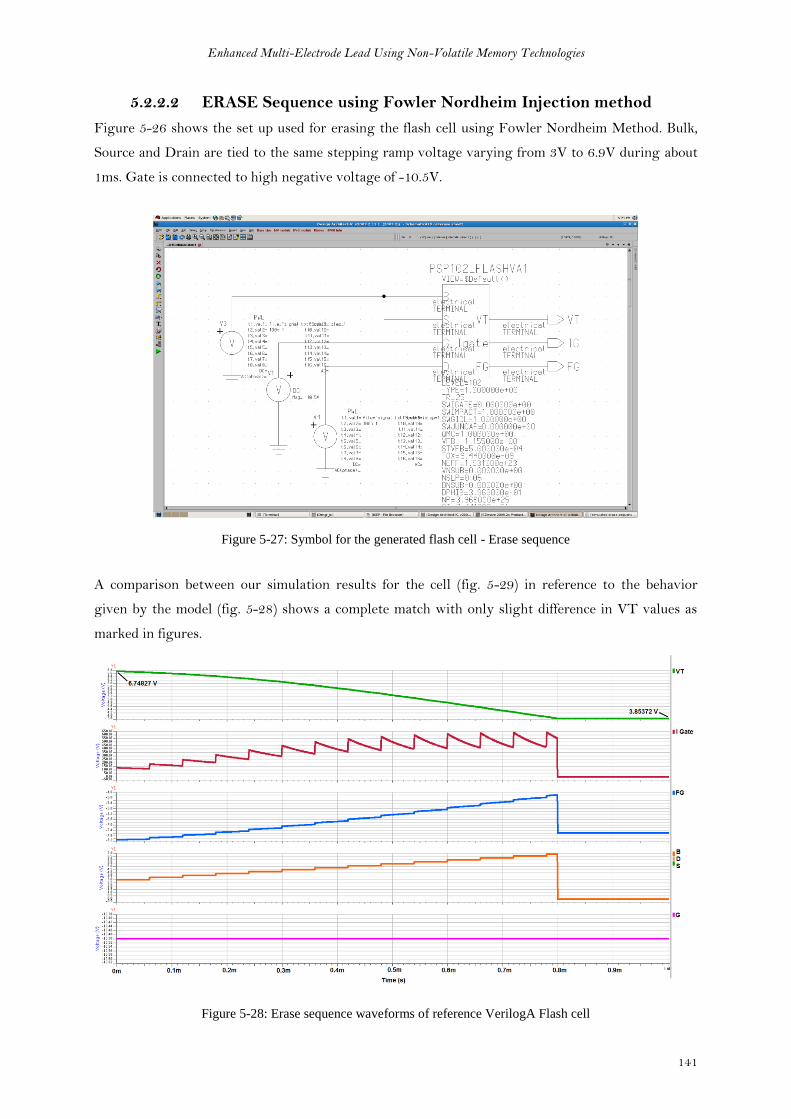
Enhanced Multi-Electrode Lead Using Non-Volatile Memory Technologies
141
5.2.2.2 ERASE Sequence using Fowler Nordheim Injection method
Figure 5-26 shows the set up used for erasing the flash cell using Fowler Nordheim Method. Bulk,
Source and Drain are tied to the same stepping ramp voltage varying from 3V to 6.9V during about
1ms. Gate is connected to high negative voltage of -10.5V.
Figure 5-27: Symbol for the generated flash cell - Erase sequence
A comparison between our simulation results for the cell (fig. 5-29) in reference to the behavior
given by the model (fig. 5-28) shows a complete match with only slight difference in VT values as
marked in figures.
Figure 5-28: Erase sequence waveforms of reference VerilogA Flash cell
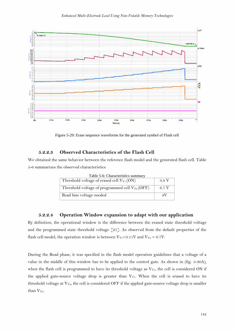
Enhanced Multi-Electrode Lead Using Non-Volatile Memory Technologies
142
Figure 5-29: Erase sequence waveforms for the generated symbol of Flash cell
5.2.2.3 Observed Characteristics of the Flash Cell
We obtained the same behavior between the reference flash model and the generated flash cell. Table
5-6 summarizes the observed characteristics
Table 5-6: Characteristics summary
Threshold voltage of erased cell VT1 (ON) 3.8 V
Threshold voltage of programmed cell VT2 (OFF) 6.7 V
Read bias voltage needed 4V
5.2.2.4 Operation Window expansion to adapt with our application
By definition, the operational window is the difference between the erased state threshold voltage
and the programmed state threshold voltage [21]. As observed from the default properties of the
flash cell model, the operation window is between VT1=3.11V and VT2 = 6.7V.
During the Read phase, it was specified in the flash model operation guidelines that a voltage of a
value in the middle of this window has to be applied to the control gate. As shown in (fig. 5-30A),
when the flash cell is programmed to have its threshold voltage as VT1, the cell is considered ON if
the applied gate-source voltage drop is greater than VT1. When the cell is erased to have its
threshold voltage at VT2, the cell is considered OFF if the applied gate-source voltage drop is smaller
than VT2.
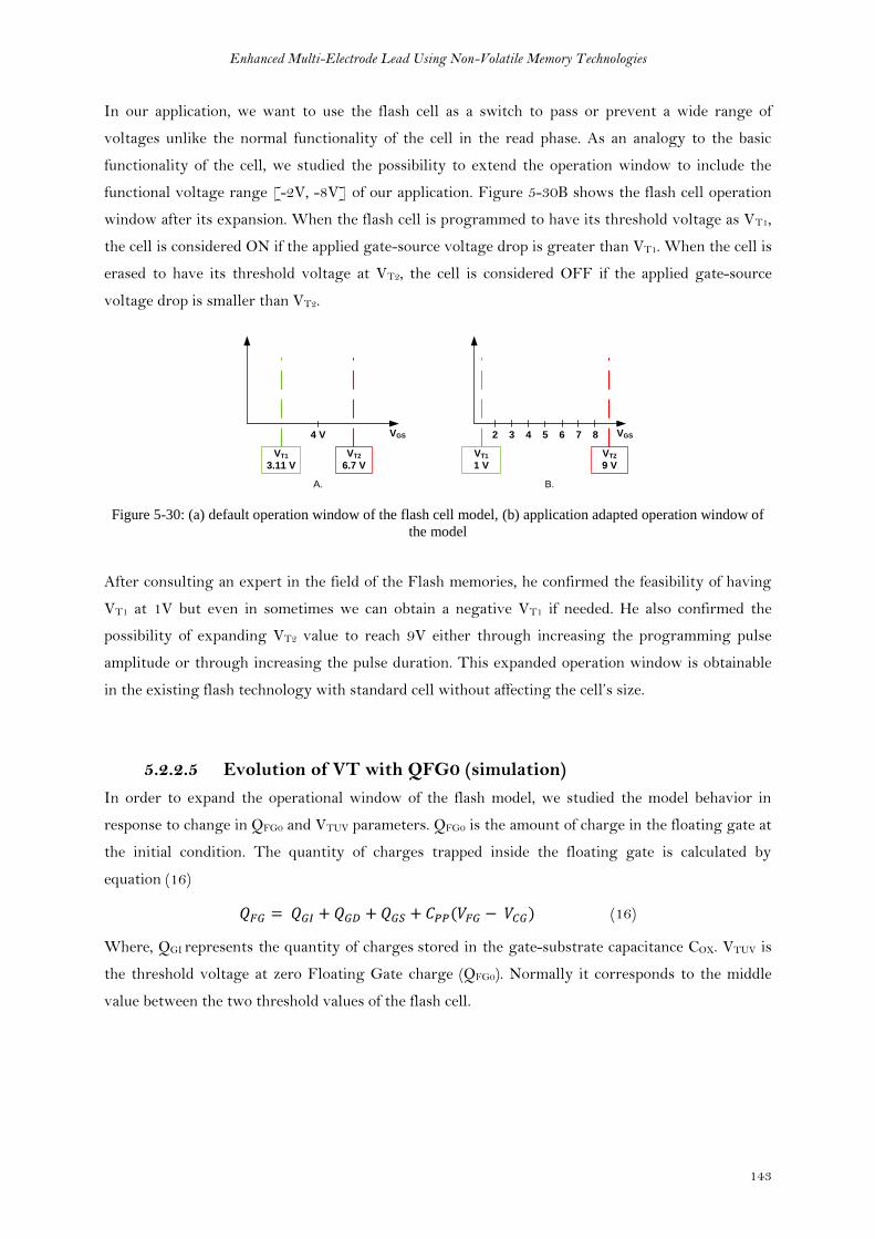
Enhanced Multi-Electrode Lead Using Non-Volatile Memory Technologies
143
In our application, we want to use the flash cell as a switch to pass or prevent a wide range of
voltages unlike the normal functionality of the cell in the read phase. As an analogy to the basic
functionality of the cell, we studied the possibility to extend the operation window to include the
functional voltage range [-2V, -8V] of our application. Figure 5-30B shows the flash cell operation
window after its expansion. When the flash cell is programmed to have its threshold voltage as VT1,
the cell is considered ON if the applied gate-source voltage drop is greater than VT1. When the cell is
erased to have its threshold voltage at VT2, the cell is considered OFF if the applied gate-source
voltage drop is smaller than VT2.
VT1
3.11 V
VT2
6.7 V
4 V VGS
VT1
1 V
VT2
9 V
2 3 4 5 6 7 8 VGS
A. B.
Figure 5-30: (a) default operation window of the flash cell model, (b) application adapted operation window of
the model
After consulting an expert in the field of the Flash memories, he confirmed the feasibility of having
VT1 at 1V but even in sometimes we can obtain a negative VT1 if needed. He also confirmed the
possibility of expanding VT2 value to reach 9V either through increasing the programming pulse
amplitude or through increasing the pulse duration. This expanded operation window is obtainable
in the existing flash technology with standard cell without affecting the cell’s size.
5.2.2.5 Evolution of VT with QFG0 (simulation)
In order to expand the operational window of the flash model, we studied the model behavior in
response to change in QFG0 and VTUV parameters. QFG0 is the amount of charge in the floating gate at
the initial condition. The quantity of charges trapped inside the floating gate is calculated by
equation (16)
(16)
Where, QGI represents the quantity of charges stored in the gate-substrate capacitance COX. VTUV is
the threshold voltage at zero Floating Gate charge (QFG0). Normally it corresponds to the middle
value between the two threshold values of the flash cell.

Enhanced Multi-Electrode Lead Using Non-Volatile Memory Technologies
144
The following graph (fig. 5-31) shows the evolution of threshold voltage VT with different values for
QFG0 parameter in the flash cell model.
Figure 5-31: Threshold voltage change with varying QFG0 @Vtuv = 1V
5.2.3 Non-Volatile Switching Unit Using Flash Memory Cell
We aim to use the flash cells as programmable switches to connect or disconnect each stimulation
electrode in the stimulation lead to Anode or Cathode lines. These programmable switches must be
able to support stimulation currents (16mA) and voltages (up to 8V). Moreover, these switches have
to have low ON resistance to minimize the energy loss in the path between the pacemaker and the
patient’s heart.
At this important amount of currents, the flash cell risks to be damaged. We found that the flash
cells could not be used alone to replace stimulation switches as was the case with NRAM cell of
section 5.2 of this chapter.
We thought of architecture for a nonvolatile switching unit in which flash cells are to be associated
to ordinary MOS transistors. According to the state of the flash cell ON or OFF, it will drive the
MOS transistor to block or pass the stimulation signal between the pacemaker and the configured
electrode.
0
2
4
6
8
10
-1 -0,8 -0,6 -0,4 -0,2 0
QFG0 (x 10-15)
VT
VT
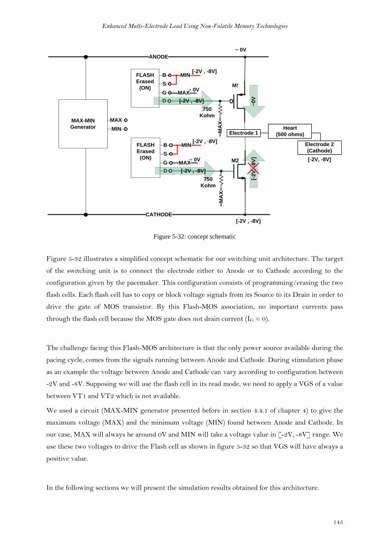
Enhanced Multi-Electrode Lead Using Non-Volatile Memory Technologies
145
CATHODE
ANODE
~0
V
FLASH
Erased
(ON)
B
S
G
D
Electrode 1Heart
(500 ohms)
~ 0V
MIN[-2V , -8V]
MAX
[-2V , -8V]
Electrode 2
(Cathode)
[-2V , -8V]
[-2V, -8V]
750
Kohm
[-2
V, -8
V]
FLASH
Erased
(ON)
B
S
G
D
~ 0V
MIN[-2V , -8V]
MAX
[-2V , -8V]
750
Kohm
MA
XM
AX
~ 0V
M!
M2
MAX-MIN
Generator
MAX
MIN
Figure 5-32: concept schematic
Figure 5-32 illustrates a simplified concept schematic for our switching unit architecture. The target
of the switching unit is to connect the electrode either to Anode or to Cathode according to the
configuration given by the pacemaker. This configuration consists of programming/erasing the two
flash cells. Each flash cell has to copy or block voltage signals from its Source to its Drain in order to
drive the gate of MOS transistor. By this Flash-MOS association, no important currents pass
through the flash cell because the MOS gate does not drain current (IG ≈ 0).
The challenge facing this Flash-MOS architecture is that the only power source available during the
pacing cycle, comes from the signals running between Anode and Cathode. During stimulation phase
as an example the voltage between Anode and Cathode can vary according to configuration between
-2V and -8V. Supposing we will use the flash cell in its read mode, we need to apply a VGS of a value
between VT1 and VT2 which is not available.
We used a circuit (MAX-MIN generator presented before in section 4.4.1 of chapter 4) to give the
maximum voltage (MAX) and the minimum voltage (MIN) found between Anode and Cathode. In
our case, MAX will always be around 0V and MIN will take a voltage value in [-2V, -8V] range. We
use these two voltages to drive the Flash cell as shown in figure 5-32 so that VGS will have always a
positive value.
In the following sections we will present the simulation results obtained for this architecture.
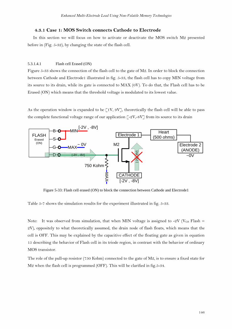
Enhanced Multi-Electrode Lead Using Non-Volatile Memory Technologies
146
4.3.1 Case 1: MOS Switch connects Cathode to Electrode
In this section we will focus on how to activate or deactivate the MOS switch M2 presented
before in (Fig. 5-32), by changing the state of the flash cell.
5.3.1.4.1 Flash cell Erased (ON)
Figure 5-33 shows the connection of the flash cell to the gate of M2. In order to block the connection
between Cathode and Electrode1 illustrated in fig. 5-33, the flash cell has to copy MIN voltage from
its source to its drain, while its gate is connected to MAX (0V). To do that, the Flash cell has to be
Erased (ON) which means that the threshold voltage is modulated to its lowest value.
As the operation window is expanded to be [1V, 9V], theoretically the flash cell will be able to pass
the complete functional voltage range of our application [-2V,-8V] from its source to its drain
FLASHErased
(ON)
B
S
G
D
Electrode 1
CATHODE
Heart
(500 ohms)
~ 0V
MIN[-2V , -8V]
MAX
[-2V , -8V]
Electrode 2
(ANODE)
[-2V , -8V]
~0V
750 Kohm
[-2
V, -8
V]
M2
MA
X
Figure 5-33: Flash cell erased (ON) to block the connection between Cathode and Electrode1
Table 5-7 shows the simulation results for the experiment illustrated in fig. 5-33.
Note: It was observed from simulation, that when MIN voltage is assigned to -2V (VGS Flash =
2V), oppositely to what theoretically assumed, the drain node of flash floats, which means that the
cell is OFF. This may be explained by the capacitive effect of the floating gate as given in equation
15 describing the behavior of Flash cell in its triode region, in contrast with the behavior of ordinary
MOS transistor.
The role of the pull-up resistor (750 Kohm) connected to the gate of M2, is to ensure a fixed state for
M2 when the flash cell is programmed (OFF). This will be clarified in fig.5-34.
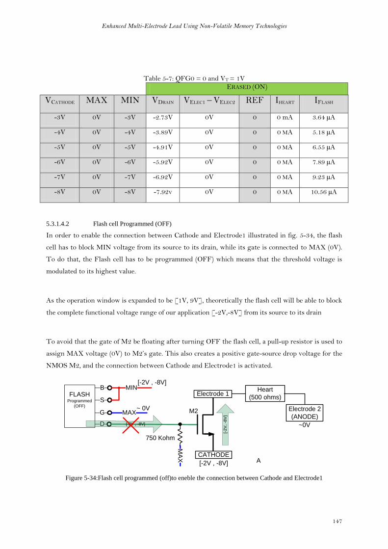
Enhanced Multi-Electrode Lead Using Non-Volatile Memory Technologies
147
Table 5-7: QFG0 = 0 and VT = 1V ERASED (ON)
VCATHODE MAX MIN VDRAIN VELEC1 – VELEC2 REF IHEART IFLASH
-3V 0V -3V -2.73V 0V 0 0 mA 3.64 µA
-4V 0V -4V -3.89V 0V 0 0 MA 5.18 µA
-5V 0V -5V -4.91V 0V 0 0 MA 6.55 µA
-6V 0V -6V -5.92V 0V 0 0 MA 7.89 µA
-7V 0V -7V -6.92V 0V 0 0 MA 9.23 µA
-8V 0V -8V -7.92v 0V 0 0 MA 10.56 µA
5.3.1.4.2 Flash cell Programmed (OFF)
In order to enable the connection between Cathode and Electrode1 illustrated in fig. 5-34, the flash
cell has to block MIN voltage from its source to its drain, while its gate is connected to MAX (0V).
To do that, the Flash cell has to be programmed (OFF) which means that the threshold voltage is
modulated to its highest value.
As the operation window is expanded to be [1V, 9V], theoretically the flash cell will be able to block
the complete functional voltage range of our application [-2V,-8V] from its source to its drain
To avoid that the gate of M2 be floating after turning OFF the flash cell, a pull-up resistor is used to
assign MAX voltage (0V) to M2’s gate. This also creates a positive gate-source drop voltage for the
NMOS M2, and the connection between Cathode and Electrode1 is activated.
FLASHProgrammed
(OFF)
B
S
G
D
Electrode 1
CATHODE
Heart
(500 ohms)
~ 0V
MIN[-2V , -8V]
MAXElectrode 2
(ANODE)
[-2V , -8V]
~0V
[-2
V, -8
V]
750 Kohm
[-2V , -8V]
M2
A
MA
X
Figure 5-34:Flash cell programmed (off)to eneble the connection between Cathode and Electrode1
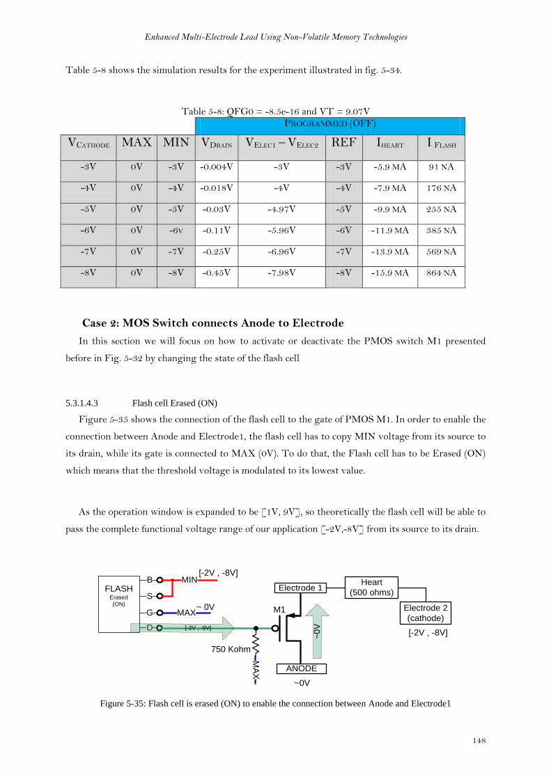
Enhanced Multi-Electrode Lead Using Non-Volatile Memory Technologies
148
Table 5-8 shows the simulation results for the experiment illustrated in fig. 5-34.
Table 5-8: QFG0 = -8.5e-16 and VT = 9.07V PROGRAMMED (OFF)
VCATHODE MAX MIN VDRAIN VELEC1 – VELEC2 REF IHEART I FLASH
-3V 0V -3V -0.004V -3V -3V -5.9 MA 91 NA
-4V 0V -4V -0.018V -4V -4V -7.9 MA 176 NA
-5V 0V -5V -0.03V -4.97V -5V -9.9 MA 255 NA
-6V 0V -6v -0.11V -5.96V -6V -11.9 MA 385 NA
-7V 0V -7V -0.25V -6.96V -7V -13.9 MA 569 NA
-8V 0V -8V -0.45V -7.98V -8V -15.9 MA 864 NA
Case 2: MOS Switch connects Anode to Electrode
In this section we will focus on how to activate or deactivate the PMOS switch M1 presented
before in Fig. 5-32 by changing the state of the flash cell
5.3.1.4.3 Flash cell Erased (ON)
Figure 5-35 shows the connection of the flash cell to the gate of PMOS M1. In order to enable the
connection between Anode and Electrode1, the flash cell has to copy MIN voltage from its source to
its drain, while its gate is connected to MAX (0V). To do that, the Flash cell has to be Erased (ON)
which means that the threshold voltage is modulated to its lowest value.
As the operation window is expanded to be [1V, 9V], so theoretically the flash cell will be able to
pass the complete functional voltage range of our application [-2V,-8V] from its source to its drain.
FLASHErased
(ON)
B
S
G
D
Electrode 1
ANODE
Heart
(500 ohms)
~ 0V
MIN[-2V , -8V]
MAX
[-2V , -8V]
Electrode 2
(cathode)
[-2V , -8V]
~0V
750 Kohm
~0
V
MA
X
M1
Figure 5-35: Flash cell is erased (ON) to enable the connection between Anode and Electrode1
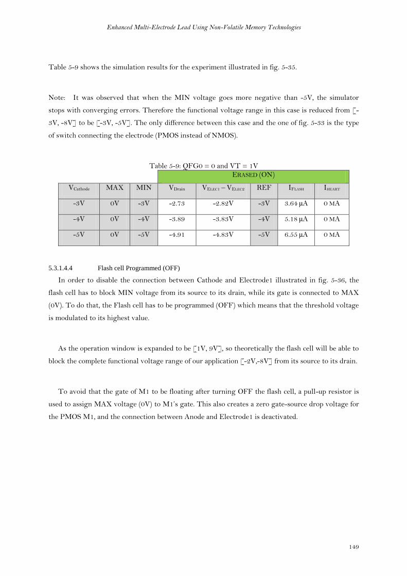
Enhanced Multi-Electrode Lead Using Non-Volatile Memory Technologies
149
Table 5-9 shows the simulation results for the experiment illustrated in fig. 5-35.
Note: It was observed that when the MIN voltage goes more negative than -5V, the simulator
stops with converging errors. Therefore the functional voltage range in this case is reduced from [-
3V, -8V] to be [-3V, -5V]. The only difference between this case and the one of fig. 5-33 is the type
of switch connecting the electrode (PMOS instead of NMOS).
Table 5-9: QFG0 = 0 and VT = 1V ERASED (ON)
VCathode MAX MIN VDrain VELEC1 – VELEC2 REF IFLASH IHEART
-3V 0V -3V -2.73 -2.82V -3V 3.64 µA 0 MA
-4V 0V -4V -3.89 -3.83V -4V 5.18 µA 0 MA
-5V 0V -5V -4.91 -4.83V -5V 6.55 µA 0 MA
5.3.1.4.4 Flash cell Programmed (OFF)
In order to disable the connection between Cathode and Electrode1 illustrated in fig. 5-36, the
flash cell has to block MIN voltage from its source to its drain, while its gate is connected to MAX
(0V). To do that, the Flash cell has to be programmed (OFF) which means that the threshold voltage
is modulated to its highest value.
As the operation window is expanded to be [1V, 9V], so theoretically the flash cell will be able to
block the complete functional voltage range of our application [-2V,-8V] from its source to its drain.
To avoid that the gate of M1 to be floating after turning OFF the flash cell, a pull-up resistor is
used to assign MAX voltage (0V) to M1’s gate. This also creates a zero gate-source drop voltage for
the PMOS M1, and the connection between Anode and Electrode1 is deactivated.
Enhanced Multi-Electrode Lead Using Non-Volatile Memory Technologies
150
FLASHProgrammed
(OFF)
B
S
G
D
Electrode 1
ANODE
Heart
(500 ohms)
~ 0V
MIN[-2V , -8V]
MAXElectrode 2
(Cathode)
[-2V , -8V]
~0V
~0
V
750 Kohm
[-2V , -8V]
MA
X
A
M1
Figure 5-36: Flash cell is programmed to block the connection between Anode and Electrode1
Table 5-10 shows the simulation results for the experiment illustrated in fig. 5-36.
Table 5-10: QFG0 = -8.5e-16 and VT = 9.07V PROGRAMMED (OFF)
VCathode MAX MIN V Drain VELEC1 – VELEC2 REF I HEART I FLASH
-3V 0V -3V 0V 0V 0V 0 MA 2.91 NA
-4V 0V -4V -0.01V 0V 0V 0 MA 13.7 NA
-5V 0V -5V -0.03V 0V 0V 0 MA 52.11 NA
-6V 0V -6V -0.11V 0V 0V 0 MA 151 NA
-7V 0V -7V -0.25V 0V 0V 0 MA 336 NA
-8V 0V -8V -0.45V 0V 0V 0 MA 604 NA
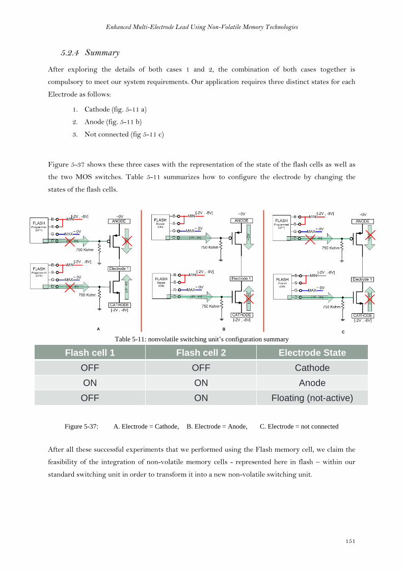
Enhanced Multi-Electrode Lead Using Non-Volatile Memory Technologies
151
5.2.4 Summary
After exploring the details of both cases 1 and 2, the combination of both cases together is
compulsory to meet our system requirements. Our application requires three distinct states for each
Electrode as follows:
1. Cathode (fig. 5-11 a)
2. Anode (fig. 5-11 b)
3. Not connected (fig 5-11 c)
Figure 5-37 shows these three cases with the representation of the state of the flash cells as well as
the two MOS switches. Table 5-11 summarizes how to configure the electrode by changing the
states of the flash cells.
Flash cell 1 Flash cell 2 Electrode State
OFF OFF Cathode
ON ON Anode
OFF ON Floating (not-active)
Figure 5-37: A. Electrode = Cathode, B. Electrode = Anode, C. Electrode = not connected
After all these successful experiments that we performed using the Flash memory cell, we claim the
feasibility of the integration of non-volatile memory cells - represented here in flash – within our
standard switching unit in order to transform it into a new non-volatile switching unit.
Table 5-11: nonvolatile switching unit’s configuration summary
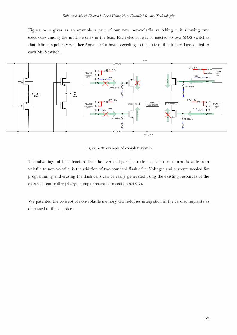
Enhanced Multi-Electrode Lead Using Non-Volatile Memory Technologies
152
Figure 5-38 gives as an example a part of our new non-volatile switching unit showing two
electrodes among the multiple ones in the lead. Each electrode is connected to two MOS switches
that define its polarity whether Anode or Cathode according to the state of the flash cell associated to
each MOS switch.
~0
V ~0V
FLASHProgrammed
(OFF)
B
S
G
D
Electrode 1Heart
(500 ohms)
~ 0V
MIN[-2V , -8V]
MAX
FLASHErased
(ON)
B
S
G
D
Electrode 2
~ 0V
MIN[-2V , -8V]
MAX
[-2V , -8V]
[-2
V, -8
V]
750 Kohm 750 Kohm
[-2
V,
-8V
]
[-2V , -8V]
FLASHProgrammed
(OFF)
B
S
G
D
~ 0V
MIN[-2V , -8V]
MAX
750 Kohm
[-2V , -8V]
FLASHErased
(ON)
B
S
G
D
~ 0V
MIN[-2V , -8V]
MAX
[-2V , -8V]
750 Kohm
MA
XM
AX
MA
XM
AX
MAX
CATHODE
ANODE
MIN
[-2V , -8V]
~ 0V
Figure 5-38: example of complete system
The advantage of this structure that the overhead per electrode needed to transform its state from
volatile to non-volatile; is the addition of two standard flash cells. Voltages and currents needed for
programming and erasing the flash cells can be easily generated using the existing resources of the
electrode-controller (charge pumps presented in section 3.4.2.7).
We patented the concept of non-volatile memory technologies integration in the cardiac implants as
discussed in this chapter.
Enhanced Multi-Electrode Lead Using Non-Volatile Memory Technologies
153
5.3 Conclusion
In this chapter we opened a new direction for research through the integration of rising nonvolatile
memory technologies within cardiac stimulation system. The employment of such technologies in
building a new non-volatile switching unit enhanced our multi-electrode system in several aspects. It
suppressed the need of repetitive configuration of electrodes as long as change is not required which
is built on its capability of state retention for unlimited durations. It also reduced the latency
between stimulation demand and its delivery to the electrodes. Moreover, it alleviates the need of big
power storage unit which reduces the overall size of electrode controller. It was also noticed that
nonvolatile memory cells are smaller in size than low Ron MOS switches used in conventional
switching units.
We saw how promising a technology like NRAM can be for our application. It’s no leakage states,
very big resistance distinction between its states; speed and small size make it the ideal candidate for
our application.
STT MTJ and Memristance were grouped under resistive RAM family for their common features
from the application point of view. After our investigations, we reached a conclusion that their
integration in our system is not feasible due to their states instability facing stimulation voltages and
currents.
Finally we investigated flash memory cells and came up with a new structure where flash cells are
associated with MOS transistors. In this structure stimulation voltages and currents passes through
the MOS transistors while the flash cells define and retain the state of the MOS transistor.
We patented the concept of non-volatile memory technologies integration in the cardiac implants as
discussed in this chapter.
Publications
Patent N° FR1159288, « Module de commutation contrôlée de sonde multiélectrode pour un
dispositif médical implantable actif », filed one 13 October 2011
Enhanced Multi-Electrode Lead Using Non-Volatile Memory Technologies
154
References
[1] Ch. Muller et al. “Design challenges for prototypical and emerging memory concepts relying on
resistance switching” 978-1-4577-0223-5
[2] W guo, G Prenat, V Javerliac, M El Baraji, N de Mestier, C baraduc and B Dieny “SPICE
modeling of magnetic tunnel junctions written by spin-transfer torque”. J. Phys. D: Appl. Phys. 43
(2010) 215001
[3] Jonathan F. Harms et al. “Spice macromodel of spin-torque-transfer-operated magnetic tunnel
junctions” IEEE transactions on electron devices, vol. 57, no. 6, june 2010
[4] Dynamic compact model of Spin-Transfer Torque based magnetic tunnel junction (MTJ) (ref.
Louis-barthelemy Faber et al “Dynamic compact model of Spin-Transfer Torque based magnetic
tunnel junction (MTJ)” 2009 IEEE)
[5] Dmitri B. Strukov, Gregory S. Snider, Duncan R. Stewart and R. Stanley Williams: “The
missing memristor found”
[6] Dalibor Biolek, Zdenek Biolek, Viera Biolkova: “SPICE Modeling of Memristive,
Memcapacitative and Meminductive Systems”
[7] Massimiliano Di Ventra, Yuriy V. Pershin, and Leon O. Chua: “Circuit Elements with Memory:
Memristors, Memcapacitors, and Meminductors”
[8] Tezaswi Raja and Samiha Mourad: “Digital Logic Implementation in Memrstor-based
Crossbars”
[9] Yenpo Ho, Garng M. Huang and Peng Li: “Nonvolatile Memristor Memory: Device
Characteristics and design implicatons”
[10] Sangho Shin, Kyungmin Kim and Sung-Mo Kang “Memristor-Based Fine Resolution
Programmable Resistance and Its Applications”
[11] EVER SPIN TECHNOLOGIE S, IN C. MRAM Technical guide
[12] MR2A16A Datasheet
[13] J. P. Nozières « Magnetic Random Access Memories (M-RAM): A truly universal memory? »
[14] B. N. Engel, J. Åkerman, B. Butcher, R. W. Dave, M. DeHerrera, M. Durlam, G. Grynkewich,
J. Janesky, S. V. Pietambaram, N. D. Rizzo, J. M. Slaughter, K. Smith, J. J. Sun, and S. Tehrani “A 4-
Mb Toggle MRAM Based on a Novel Bit and Switching Method”
[15] US Patent 6545906
[16] R.F. Smith, T. Ruekes, S. Konsek, J.W. Ward, D.K. Brock, and B.M. Segal “Carbon Nanotube
Based Memory Development and Testing”
Enhanced Multi-Electrode Lead Using Non-Volatile Memory Technologies
155
[17] Thomas Rueckes, Kyoungha Kim, Ernesto Joselevich, Greg Y. Tseng, Chin-Li Cheung, and
Charles M. Lieber “Carbon Nanotube-Based Nonvolatile Random Access Memory for Molecular
Computing”
[18] Journal of Nuclear Medicine JNM figure
[19] Daniel Batas and Horst Fiedler “A Memristor SPICE Implementation and a New Approach for
Magnetic Flux-Controlled Memristor Modeling” IEEE transactions on Nanotechnology, Vol. 10,
no. 2, March 2011
[20] A. Maure, P. Canet, F. Lalande, B. Delsuc, J. Devin « Flash Memory cell compact modelling
using PSP model » Proceedings of the IEEE BMAS, 2008
[29] S. S. Chung, S. T. Liaw, C. M. Yih, Z. H. Ho, C. J. Lin, D. S. Kuo, and M. S. Liang “N-channel
versus p-channel Flash EEPROM – which one has better reliabilities” Reliability Physics
Symposium, 2001.
[22] Nantero, Inc. “Mass Insight PowerPoint” 2005
[23] P. Pavan, R. Bez, P. Olivo, E. Zanoni “Flash Memory Cells – An Overview” Proceedings of the
IEEE, vol. 85, no. 8, august 1997
[24] US Patent 7652337 “Nanotube-based switching element”, Nantero Inc. 2006

Enhanced Multi-Electrode Lead Using Non-Volatile Memory Technologies
156

Conclusion
157
6 Chapter 6
Conclusion
Conclusion
158
This thesis started by presenting the structure of human heart and the different disorders affecting it
that may raise the need for cardiac implants. We saw how cardiac implants evolution led to better
treatment for patients suffering from cardiovascular diseases. We then explored the building blocks
of cardiac implants and how they interact with cardiac tissues to analyze the patient’s state and
deliver the adequate treatment. By the end of chapter 2, the importance of biventricular pacing
(CRT) was cleared as well as the limitations of using bipolar leads in left ventricular stimulation.
In chapter 3, we addressed those limitations by our multi-electrode system for left ventricular
stimulation. We presented this system in its two structures (centralized and distributed). We showed
how we modified the implant’s control in order to drive our custom-designed electrode-controller
inserted inside the lead.
Our system added more flexibility for the choice of stimulation sites through its selective control of
up to 8 electrodes with the possibility of interchangeable polarity for each. The re-configurability of
lead electrodes suppresses the need for post-implant surgery in case of inhibition of patient response
to stimulation caused by lead displacement.
The communication between the two parts of our multi-electrode system (implant and the electrode-
controller) was implemented by our one-wire protocol doted by a tolerance to difference in oscillator
frequencies between both sides. According to this protocol, power pulses and configuration bits
shared the same line, leaving Anode and Cathode lines for stimulation and sensing purposes. This
enabled the isolation of patient’s heart from data and power pulses. Moreover it resulted in a norm-
compliant 3-wire connector interface.
Another notable feature in our system is its capability of delivering two consecutive stimulation
pulses of same or different polarities as configured. This feature enables biphasic stimulation which
may reduce the discharge period that follows the stimulation phase.
Our system is distinguished by ensuring compatibility of our multi-electrode lead with any
pacemaker in the market thanks to its auxiliary switching unit. The concept was proved using
discrete JFET switches.

Conclusion
159
In chapter 4 we presented an ameliorated solution for the problem of mult-electrode lead
compatibility with any pacemaker device in the market; named Default Connection Unit (DCU). This
unit which was integrated within the electrode-controller chip process alleviates this challenge by
transforming the multi-electrode lead into a standard bipolar lead through the activation of two
electrodes that it shares their control with the main switching unit found in the electrode-controller
chip.
We showed how the DCU was designed to use the available stimulation energy to activate its paths
between Anode, Cathode and default electrodes without the need for a power source (battery). It also
stores a part of this energy in order to retain its state for a period that at least covers the discharge
phase duration. DCU paths are equipped with resistances that enable it to continue ensuring the
connection between electrodes and the pacemaker during the duration of the sensing phase which
depends on each patient.
DCU distinguishes our multi-electrode system and takes a step forward compared to the auxiliary
switching unit using JFET presented in chapter 3 as it is integrated in the technology process used
in the electrode-controller chip.
As the DCU is assigned to only two electrodes in the multi-electrode lead, this may show some
limitations to the site of stimulation for the new pacemaker connected to the lead. In chapter 5 we
introduced a new solution to address this issue. We showed how nonvolatile memories and its
underlying implementation technologies offer us ways to maintain the last configured stimulation
site and thereby allowing us to circumvent the fixed site limitation imposed by the DCU.
This opened a new direction for research through the integration of rising nonvolatile memory
technologies within cardiac stimulation system. The employment of such technologies in building a
new non-volatile switching unit enhanced our multi-electrode system in several aspects. It
suppressed the need of repetitive configuration of electrodes as long as change is not required which
is built on its capability of state retention for unlimited durations. It also reduced the latency
between stimulation demand and its delivery to the electrodes. Moreover, it alleviates the need of big
power storage unit which reduces the overall size of electrode controller. It was also noticed that
nonvolatile memory cells are smaller in size than low Ron MOS switches used in conventional
switching units.

Conclusion
160
We saw how promising a technology like NRAM can be for our application. It’s no leakage states,
very big resistance distinction between its states; speed and small size make it the ideal candidate for
our application.
STT MTJ and Memristance were grouped under resistive RAM family for their common features
from the application point of view. After our investigations, we reached a conclusion that their
integration in our system is not feasible due to their states instability facing stimulation voltages and
currents.
Finally we investigated flash memory cells and came up with a new structure where flash cells are
associated with MOS transistors. In this structure stimulation voltages and currents passes through
the MOS transistors while the flash cells define and retain the state of the MOS transistor.
We patented the concept of non-volatile memory technologies integration in the cardiac implants.
We believe much work can be done at all levels in the multi-electrode system. While there are new
technologies which need to be explored in more detail through silicon proven chips and
characterization, even the traditional approach can be improved by re-looking at the design aspects.
For example we can rethink the communication protocol in the multi-electrode lead; we can also
reexamine the circuit implementations of the analog/digital blocks of our system. In the non-volatile
memories, we can investigate the design of circuitry used for programming and erasing memory
cells. This make the system more integrated hence electronically more performant.
As technology matures and new technologies come to the fore and new solutions to manage
cardiovascular ailments will come into being. Like any technology design, there would be elements
of tradeoff; some approaches will offer better power consumption figures versus others which are
more performant. Moreover, as we saw in the previous chapters, technologies are in different states
of maturity and one of the key elements of industrial design is to judiciously select the technologies
and make design decisions which are backward compatible and take less implementation time. The
experience gained during the thesis has helped us to understand these subtle choices and look at new
approaches with a pragmatic angle.
Conclusion
161
List of Publications
1. I. Seoudi, K. Amara, F. Gayral, A. Amara, R. Dal Molin “Multi-electrode system for
pacemaker applications” IEEE ICECS 2011
http://ieeexplore.ieee.org/xpl/freeabs_all.jsp?arnumber=6122230
2. I. Seoudi, K. Amara, F. Gayral, A. Amara, R. Dal Molin “Innovative Multi-electrode
Communication Scheme for Cardiac Pacemakers” TBME 2012 (submitted – under
review)
3. I. Seoudi, J-F. Debroux, M. Laflutte, A. Makdissi, K. Amara, A. Amara, R. Dal
Molin “Default connection in multi-electrode leads for cardiac pacemakers” accepted in
NEWCAS 17-20 June 2012
4. Patent N° FR1159288, « Module de commutation contrôlée de sonde multiélectrode
pour un dispositif médical implantable actif », filed one 13 October 2011