Embed Size (px)
Citation preview
AVERTISSEMENT
Ce document est le fruit d'un long travail approuvé par le jury de soutenance et mis à disposition de l'ensemble de la communauté universitaire élargie. Il est soumis à la propriété intellectuelle de l'auteur. Ceci implique une obligation de citation et de référencement lors de l’utilisation de ce document. D'autre part, toute contrefaçon, plagiat, reproduction illicite encourt une poursuite pénale. Contact : [email protected]
LIENS Code de la Propriété Intellectuelle. articles L 122. 4 Code de la Propriété Intellectuelle. articles L 335.2- L 335.10 http://www.cfcopies.com/V2/leg/leg_droi.php http://www.culture.gouv.fr/culture/infos-pratiques/droits/protection.htm
UNIVERSITE DE LORRAINE
Ecole Doctorale : Énergie Mécanique Matériaux
Institut Jean Lamour Département Chimie et Physique des Solides et des Surfaces
THESE résumé étendu
présentée le 18/07/2014
pour obtenir le grade de Docteur de l’Université de Lorraine
Spécialité Science des matériaux
par
Arindam JANA
Collage et adhérence de particules dans le domaine de la sous-monocouche
Jury
Président : Mohammed BELMAHI Professeur, Université de Lorraine Rapporteurs: Laurent HOUSSIAU Professeur, Université de Namur, Belgique. Pascal BRAULT Directeur de recherches CNRS, GREMI, Université d’Orléans. Examinateur: Kai NORDLUND Professeur, Université de Helsinki, Finlande. Encadrants : Gérard HENRION Directeur de recherches CNRS, IJL, Université de Lorraine Patrick PHILIPP Chargé de projets, CRP Gabriel Lippmann, Belvaux, Luxembourg.

1
Sommaire
Préambule ........................................................................................................................ 3
1 Introduction - Contexte ................................................................................................. 3
2 Aspects expérimentaux et numériques .......................................................................... 5
3 Simulation par dynamique moléculaire du dépôt de carbone ........................................ 7
Atome de carbone unique .............................................................................................. 7 3.1
Flux d’atomes de carbone ............................................................................................ 10 3.2
4 Dépôt de titane sur silicium ......................................................................................... 15
5 Dépôt de tungstène sur silicium ................................................................................... 19
6 Conclusion et perspectives .......................................................................................... 23
Conclusion ................................................................................................................... 23 6.1
Perspectives ................................................................................................................. 25 6.2

2
3
Préambule
Le manuscrit original étant écrit en langue anglaise, nous présentons ici un résumé étendu du travail
de thèse. Le manuscrit original figure en seconde partie de ce document.
Nous tenons à remercier ici le Président de l’Université de Lorraine et la Vice-Présidente du Conseil
Scientifique de l’Université de Lorraine de nous avoir permis de déroger à la règle de rédaction en
langue française.
1 Introduction - Contexte
Dans le domaine des traitements de surface, le collage et le réarrangement d’atomes dans le
domaine de la sous-monocouche revêtent une importance essentielle, la première monocouche
définissant les propriétés de l’interface entre la couche déposée et le substrat.
La maitrise de cette interface est primordiale, en particulier pour la réalisation reproductible de
dépôts possédant une bonne adhérence. Ceci représente en effet un enjeu industriel dans de nombreux
secteurs d’activité tels que la micro-électronique, le photovoltaïque, la protection contre l’usure ou la
corrosion, les barrières thermiques, la décoration, etc.
Ces aspects sont au cœur du projet “Sub-ML” qui constitue la cadre de cette thèse et dont les
objectifs principaux visent à une meilleure compréhension des mécanismes de dépôt, et plus
particulièrement du comportement de particules arrivant sur une surface de silicium. Dans ce cadre,
l’objectif de cette thèse - partie intégrante de Sub-ML - est d’étudier le collage et le réarrangement
d’atomes et l’effet de certains paramètres sur le processus de dépôt et les propriétés d’interface.
Pour atteindre ces objectifs, nous avons utilisé une approche multidisciplinaire combinant
simulations numériques (dynamique moléculaire, calculs DFT), études expérimentales (dépôts PVD)
et caractérisation des matériaux (SIMS).
Les études de collage et de réorganisation de surface ont concernées trois espèces particulières,
carbone, titane et tungstène, présentant un intérêt particulier pour la croissance de couches minces de
type carbure. Le dépôt de carbone a été étudié uniquement de manière numérique ; titane et tungstène
ont fait l’objet d’une étude numérique et expérimentale.
4
Le mémoire complet comporte 150 pages et 158 références bibliographiques. Il est structuré en
cinq chapitres. Le premier dresse un état de l’art des différentes techniques utilisées avec une attention
particulière aux travaux publiés concernant l’interaction d’un atome-projectile avec une surface cible.
Les détails des techniques expérimentales et numériques mises en œuvre au cours de cette thèse
font l’objet du second chapitre. Les trois chapitres suivants traitent du collage d’atomes sur une
surface de silicium : carbone (chap. 3), titane (chap. 4) et tungstène (chap. 5).
Une conclusion générale et des perspectives à ce travail complètent le mémoire.
5
2 Aspects expérimentaux et numériques
Les études expérimentales ont été réalisées grâce à l’instrument storing matter qui permet de
réaliser des dépôts par pulvérisation cathodique sur un collecteur en silicium. Ce collecteur est ensuite
analyser par SIMS. L’analyse se fait ainsi en connaissant parfaitement le support du dépôt et donc en
s’affranchissant des effets de matrice. Toutefois, les particules pulvérisées de la cible arrivent sur le
collecteur avec une distribution d’angles d’incidence (en fait dans un certain angle solide) et une
distribution en énergie inconnue. De ce fait, les comparaisons avec les résultats de simulation
numériques peuvent parfois être délicates.
Concernant les études de simulations numériques, celles-ci ont été réalisées par dynamique
moléculaire, cette méthode étant un outil des plus prometteurs pour aboutir à une description
prédictive du système étudié sur un court intervalle de temps. Elle fournit également des informations
détaillées des mécanismes à l’échelle atomique durant le processus de dépôt. Nous avons utilisé le
code de dynamique moléculaire FLX développé par J. Kieffer et al.1 pour modéliser le comportement
des matériaux ayant un caractère mixte covalent-ionique. FLX offre un choix de modèles
d’interaction incluant Lennard-Jones, Coulomb, Born-Mayer-Huggins, trois corps ainsi que le model
de Kieffer de transfert de charge. FLX utilise un algorithme correcteur-prédicteur de vitesse du
cinquième ordre pour l'intégration des équations de mouvement.
Le champ de potentiel de Kieffer prend la forme suivante :
∑ ∑
∑ ∑
où le premier terme du membre de droite représente l’interaction coulombienne, le second est le
potentiel répulsif de Born-Huggins-Mayer et le troisième terme représente le potentiel d’interaction
(attractif) à trois corps.
Les simulations ont été réalisées pour les conditions des particules incidentes suivantes :
Substrat : Si (100) et Si amorphe.
Espèces incidentes : C (unique et continu) ; Ti ; W.
Energie incidente : < 100 eV.
Angle d’incidence par rapport à la normale à la surface : 0 – 60°.
Paramètres calculés : rétrodiffusion, implantation, déplacement latéral, coordination, collage.
1 L. P. Huang, J. Kieffer, J. Chem. Phys. 2003, 118 (3), 1487-1498.

6
7
3 Simulation par dynamique moléculaire du dépôt de carbone
L’étude du dépôt et du collage d’atomes de carbone sur une surface de silicium a été menée en
deux parties. Dans un premier temps, nous nous sommes intéressés au comportement d’un atome de
carbone unique bombardant la surface du substrat. Dans une seconde partie, l’étude a été réalisée pour
un flux d’atomes de carbone (100 atomes dans les simulations).
Atome de carbone unique 3.1
Dans le cas de l’impact d’un atome de carbone unique, les résultats numériques obtenus à l’aide
du champ de forces défini par Kieffer ont été comparés à ceux obtenus avec ceux issus d’un calcul
utilisant les potentiels interatomique bien établis de Erhart-Albe afin de valider la méthode. Notons
que les calculs utilisant les potentiels Erhart-Albe ont été réalisés par le groupe de Kai Nordlund à
l’université d’Helsinki2
Un atome est considéré comme implanté dès lors que sa position finale dans le matériau (Si) est
est au-delà de 0,η Å de l’extrême surface (position à 0 Å). Si la position est comprise entre 0 Å et
0,5 Å, l’atome est considéré comme déposé. Si la position finale est inférieure à 0 Å, il s’agit alors des
atomes rétrodiffusés.
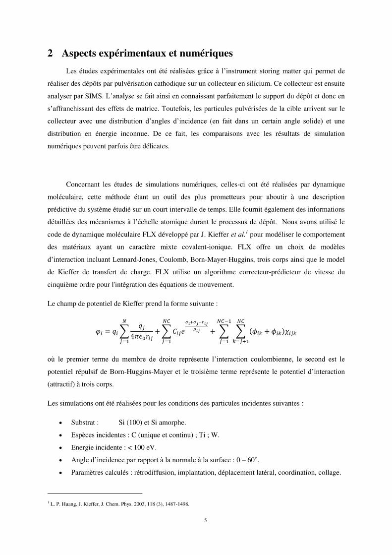
La profondeur moyenne de pénétration de l’atome de carbone est peu sensible à l’incidence de
celui-ci par rapport à la normal à la surface tant que l’énergie d’impact reste inférieure à 20 eV
(fig. 1). Pour des énergies incidentes plus élevées, la profondeur de pénétration des atomes de carbone
montre une dépendance en angle d’incidence ; pour les angles d’incidence de 30° et 4η°, les atomes
pénètrent plus profondément dans le réseau cristallin de silicium alors qu’en incidence quasi-normale
(0° et 15°) les atomes pénètrent moins dans le matériau.
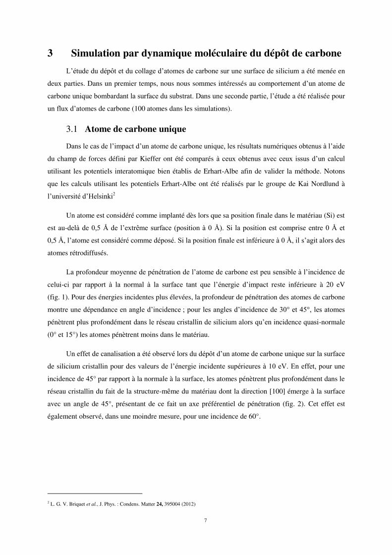
Un effet de canalisation a été observé lors du dépôt d’un atome de carbone unique sur la surface
de silicium cristallin pour des valeurs de l’énergie incidente supérieures à 10 eV. En effet, pour une
incidence de 45° par rapport à la normale à la surface, les atomes pénètrent plus profondément dans le
réseau cristallin du fait de la structure-même du matériau dont la direction [100] émerge à la surface
avec un angle de 45°, présentant de ce fait un axe préférentiel de pénétration (fig. 2). Cet effet est
également observé, dans une moindre mesure, pour une incidence de 60°.
2 L. G. V. Briquet et al., J. Phys. : Condens. Matter 24, 395004 (2012)
8
Figure 1 : Variation de la profondeur de pénétration moyenne d’un atome de carbone dans le réseau cristallin de silicium
en fonction de son énergie et pour plusieurs angles d’incidence ; simulations effectuées avec les potentiels de Kieffer et ceux de Erhart-Albe.
Figure 2: Illustration de l’effet de canalisation pour une surface de silicium dans la direction [100].
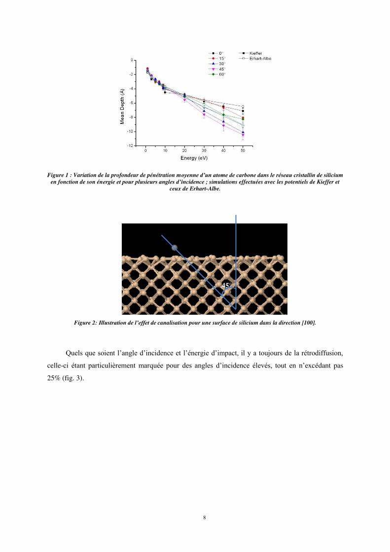
Quels que soient l’angle d’incidence et l’énergie d’impact, il y a toujours de la rétrodiffusion,
celle-ci étant particulièrement marquée pour des angles d’incidence élevés, tout en n’excédant pas
25% (fig. 3).
45°
9
Figure 3 : Probabilité de dépôt (noir), d’implantation (rouge) ou de rétrodiffusion (bleu) d’un atome de carbone sur une surface de silicium (100).
10
Flux d’atomes de carbone 3.2
Dans une seconde étape, nous nous sommes intéressés au dépôt de carbone en continu, c’est-à-
dire en simulant l’impact de plusieurs atomes successivement sur la surface de silicium cristallin. Les
simulations ont été réalisées pour les énergies d’impact de 1 à 30 eV et des angles d’incidence de 0°,
30°, 45° et 60° par rapport à la normale à la surface. Le nombre total d’atomes bombardant la surface
a été fixé à 100. Les résultats de simulation, comparé pour différentes énergies et incidences,
concernent la distribution en profondeur d’implantation, le coefficient de collage des atomes de
carbone sur silicium, la distribution de C en position radiale et angulaire par rapport au point
d’impact, ainsi que le nombre de coordination c’est-à-dire le nombre de plus proches voisins estimé
par le nombre d’atomes auxquels le carbone incident est lié à la fin de son trajet dans le matériau. De
même, les simulations permettent d’obtenir des informations précieuses sur les modifications et la
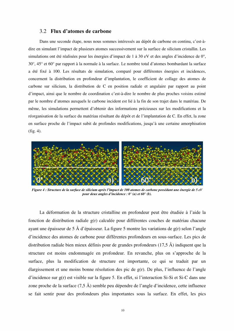
réorganisation de la surface du matériau résultant du dépôt et de l’implantation de C. En effet, la zone
en surface proche de l’impact subit de profondes modifications, jusqu’à une certaine amorphisation
(fig. 4).
Figure 4 : Structure de la surface de silicium après l’impact de 100 atomes de carbone possédant une énergie de 5 eV
pour deux angles d’incidence : 0° (a) et 60° (b).
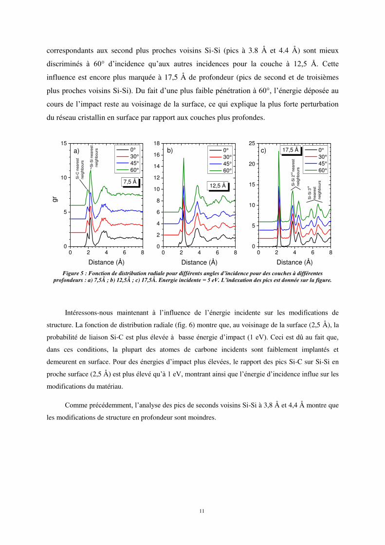
La déformation de la structure cristalline en profondeur peut être étudiée à l’aide la
fonction de distribution radiale g(r) calculée pour différentes couches de matériau chacune
ayant une épaisseur de 5 Å d’épaisseur. La figure 5 montre les variations de g(r) selon l’angle
d’incidence des atomes de carbone pour différentes profondeurs en sous-surface. Les pics de
distribution radiale bien mieux définis pour de grandes profondeurs (17,5 Å) indiquent que la
structure est moins endommagée en profondeur. En revanche, plus on s’approche de la
surface, plus la modification de structure est importante, ce qui se traduit par un
élargissement et une moins bonne résolution des pic de g(r). De plus, l’influence de l’angle
d’incidence sur g(r) est visible sur la figure η. En effet, si l’interaction Si-Si et Si-C dans une
zone proche de la surface (7,5 Å) semble peu dépendre de l’angle d’incidence, cette influence
se fait sentir pour des profondeurs plus importantes sous la surface. En effet, les pics
11
correspondants aux second plus proches voisins Si-Si (pics à 3.8 Å et 4.4 Å) sont mieux
discriminés à 60° d’incidence qu’aux autres incidences pour la couche à 12,η Å. Cette
influence est encore plus marquée à 17,5 Å de profondeur (pics de second et de troisièmes
plus proches voisins Si-Si). Du fait d’une plus faible pénétration à 60°, l’énergie déposée au
cours de l’impact reste au voisinage de la surface, ce qui explique la plus forte perturbation
du réseau cristallin en surface par rapport aux couches plus profondes.
Figure 5 : Fonction de distribution radiale pour différents angles d’incidence pour des couches à différentes
profondeurs : a) 7,5Å ; b) 12,5Å ; c) 17,5Å. Energie incidente = 5 eV. L’indexation des pics est donnée sur la figure.
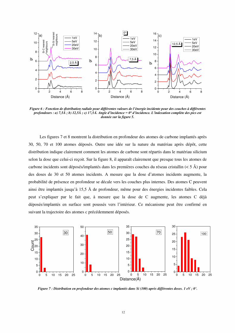
Intéressons-nous maintenant à l’influence de l’énergie incidente sur les modifications de
structure. La fonction de distribution radiale (fig. 6) montre que, au voisinage de la surface (2,5 Å), la
probabilité de liaison Si-C est plus élevée à basse énergie d’impact (1 eV). Ceci est dû au fait que,
dans ces conditions, la plupart des atomes de carbone incidents sont faiblement implantés et
demeurent en surface. Pour des énergies d’impact plus élevées, le rapport des pics Si-C sur Si-Si en
proche surface (2,5 Å) est plus élevé qu’à 1 eV, montrant ainsi que l’énergie d’incidence influe sur les
modifications du matériau.
Comme précédemment, l’analyse des pics de seconds voisins Si-Si à 3,8 Å et 4,4 Å montre que
les modifications de structure en profondeur sont moindres.
0 2 4 6 80
5
10
15
Si-S
i nea
rest
neig
hbou
rs
gr
Distance (Å)
0° 30° 45° 60°
7,5 Å
a)
Si-C
nea
rest
neig
hbou
rs
0 2 4 6 80
2
4
6
8
10
12
14
16
18
12,5 Å
Distance (Å)
0° 30° 45° 60°
b)
0 2 4 6 80
5
10
15
20
25
Si-S
i 3rd
near
est
neig
hbou
rs
Distance (Å)
0° 30° 45° 60°
17,5 Åc)
Si-S
i 2nd
near
est
neig
hbou
rs
12
Figure 6 : Fonction de distribution radiale pour différentes valeurs de l’énergie incidente pour des couches à différentes profondeurs : a) 7,5Å ; b) 12,5Å ; c) 17,5Å. Angle d’incidence = 0° d’incidence. L’indexation complète des pics est
donnée sur la figure 5.
Les figures 7 et 8 montrent la distribution en profondeur des atomes de carbone implantés après
30, 50, 70 et 100 atomes déposés. Outre une idée sur la nature du matériau après dépôt, cette
distribution indique clairement comment les atomes de carbone sont répartis dans le matériau silicium
selon la dose que celui-ci reçoit. Sur la figure 8, il apparaît clairement que presque tous les atomes de
carbone incidents sont déposés/implantés dans les premières couches du réseau cristallin (< 5 Å) pour
des doses de 30 et η0 atomes incidents. A mesure que la dose d’atomes incidents augmente, la
probabilité de présence en profondeur se décale vers les couches plus internes. Des atomes C peuvent
ainsi être implantés jusqu’à 1η,η Å de profondeur, même pour des énergies incidentes faibles. Cela
peut s’expliquer par le fait que, à mesure que la dose de C augmente, les atomes C déjà
déposés/implantés en surface sont poussés vers l’intérieur. Ce mécanisme peut être confirmé en
suivant la trajectoire des atomes c précédemment déposés.
Figure 7 : Distribution en profondeur des atomes c implantés dans Si (100) après différentes doses. 1 eV ; 0°.
0 2 4 6 80
2
4
6
8
10
12
14
16
12,5 Å
c)
gr
Distance (Å)
1eV 5eV 20eV 30eV
0 2 4 6 80
2
4
6
8
10
12
14 0°b)
7,5 Å
gr
Distance (Å)
1eV 5eV 20eV 30eV
0 2 4 6 80
2
4
6
8
10
12a)
2,5 Å
Si-S
i nea
rest
neig
hbou
rs
Si-C
nea
rest
neig
hbou
rs
gr
Distance (Å)
1eV 5eV 20eV 30eV
0 5 10 15 20 250
5
10
15
20
25
30
100
0 5 10 15 20 250
5
10
15
20
25
30
35
Distance(Å)
70
0 5 10 15 20 250
10
20
30
40
50
50
0 5 10 15 20 250
5
10
15
20
25
30
35
Cou
nt
30
13
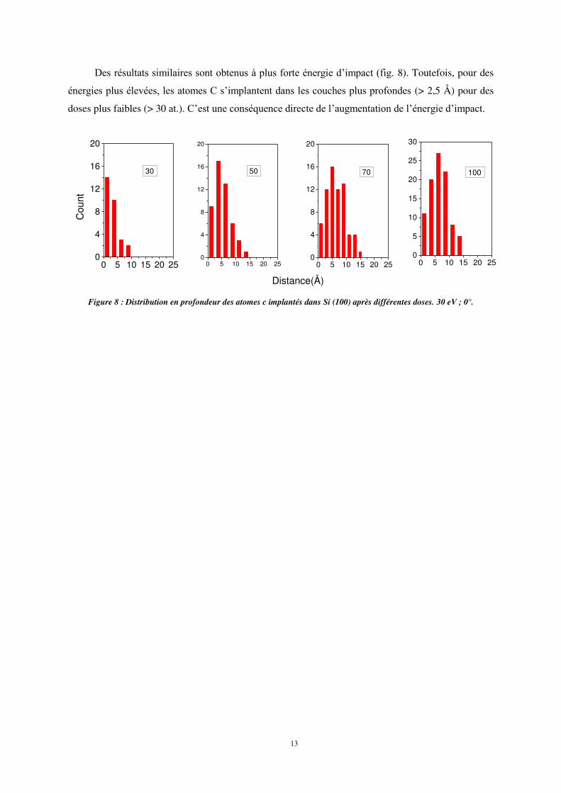
Des résultats similaires sont obtenus à plus forte énergie d’impact (fig. 8). Toutefois, pour des
énergies plus élevées, les atomes C s’implantent dans les couches plus profondes (> 2,5 Å) pour des
doses plus faibles (> 30 at.). C’est une conséquence directe de l’augmentation de l’énergie d’impact.
Figure 8 : Distribution en profondeur des atomes c implantés dans Si (100) après différentes doses. 30 eV ; 0°.
0 5 10 15 20 250
5
10
15
20
25
30
100
0 5 10 15 20 250
4
8
12
16
20
Distance(Å)
70
0 5 10 15 20 250
4
8
12
16
20
50
0 5 10 15 20 250
4
8
12
16
20
Cou
nt
30

14
15
4 Dépôt de titane sur silicium
L’un des objectifs de la partie expérimentale de ce travail est la détermination des coefficients
de collage d’atomes sur une surface de silicium cristallin. Pour cette détermination, du titane a été
déposé sur du silicium dans l’instrument Storing Matter en utilisant un faisceau d’ions argon de
10 keV. Après transfert sous ultravide, les échantillons ont été analysés par SIMS afin de déterminer
la forme des dépôts et le coefficient de collage. Un balayage de l’analyse sur la surface de
l’échantillon permet, dans un premier temps, de détermine la localisation du dépôt. Dans un second
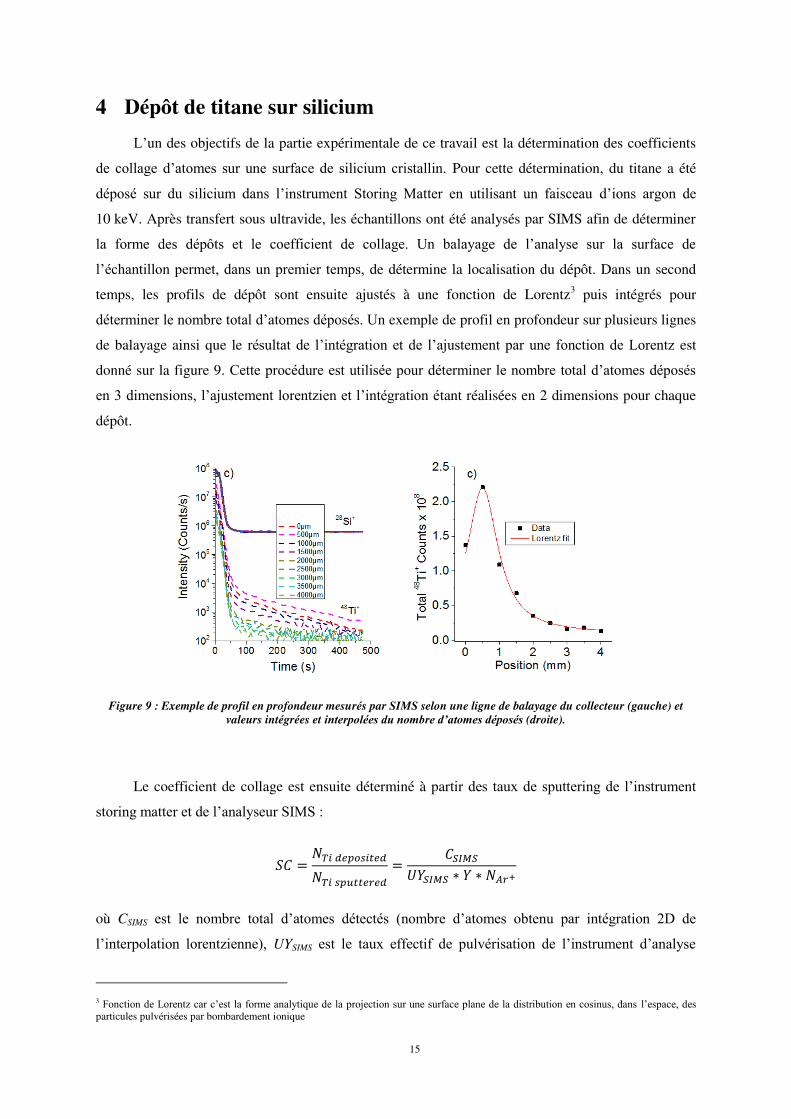
temps, les profils de dépôt sont ensuite ajustés à une fonction de Lorentz3 puis intégrés pour
déterminer le nombre total d’atomes déposés. Un exemple de profil en profondeur sur plusieurs lignes
de balayage ainsi que le résultat de l’intégration et de l’ajustement par une fonction de Lorentz est
donné sur la figure 9. Cette procédure est utilisée pour déterminer le nombre total d’atomes déposés
en 3 dimensions, l’ajustement lorentzien et l’intégration étant réalisées en 2 dimensions pour chaque
dépôt.
Figure 9 : Exemple de profil en profondeur mesurés par SIMS selon une ligne de balayage du collecteur (gauche) et valeurs intégrées et interpolées du nombre d’atomes déposés (droite).
Le coefficient de collage est ensuite déterminé à partir des taux de sputtering de l’instrument
storing matter et de l’analyseur SIMS :
où CSIMS est le nombre total d’atomes détectés (nombre d’atomes obtenu par intégration 2D de
l’interpolation lorentzienne), UYSIMS est le taux effectif de pulvérisation de l’instrument d’analyse
3 Fonction de Lorentz car c’est la forme analytique de la projection sur une surface plane de la distribution en cosinus, dans l’espace, des particules pulvérisées par bombardement ionique
16
SIMS, Y est le taux de pulvérisation de l’instrument storing mater et NAr+ le nombre d’ions Ar+ utilisés
pour réaliser le dépôt dans la chambre storing mater. NTi sputtered et NTi deposited représentent
respectivement le nombre d’atomes de titane pulvérisés de la cible et le nombre d’atomes de titane
effectivement déposés dans la chambre storing matter.
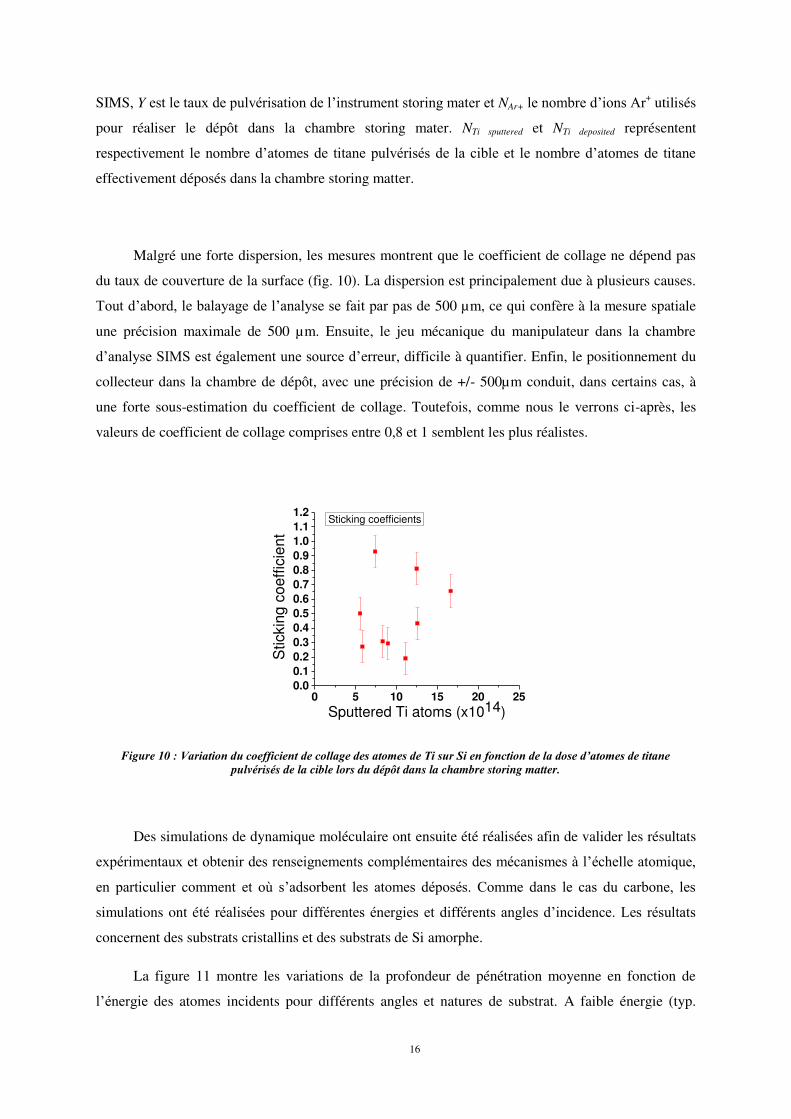
Malgré une forte dispersion, les mesures montrent que le coefficient de collage ne dépend pas
du taux de couverture de la surface (fig. 10). La dispersion est principalement due à plusieurs causes.
Tout d’abord, le balayage de l’analyse se fait par pas de 500 µm, ce qui confère à la mesure spatiale
une précision maximale de 500 µm. Ensuite, le jeu mécanique du manipulateur dans la chambre
d’analyse SIMS est également une source d’erreur, difficile à quantifier. Enfin, le positionnement du
collecteur dans la chambre de dépôt, avec une précision de +/- 500µm conduit, dans certains cas, à
une forte sous-estimation du coefficient de collage. Toutefois, comme nous le verrons ci-après, les
valeurs de coefficient de collage comprises entre 0,8 et 1 semblent les plus réalistes.
Figure 10 : Variation du coefficient de collage des atomes de Ti sur Si en fonction de la dose d’atomes de titane pulvérisés de la cible lors du dépôt dans la chambre storing matter.
Des simulations de dynamique moléculaire ont ensuite été réalisées afin de valider les résultats
expérimentaux et obtenir des renseignements complémentaires des mécanismes à l’échelle atomique,
en particulier comment et où s’adsorbent les atomes déposés. Comme dans le cas du carbone, les
simulations ont été réalisées pour différentes énergies et différents angles d’incidence. Les résultats
concernent des substrats cristallins et des substrats de Si amorphe.
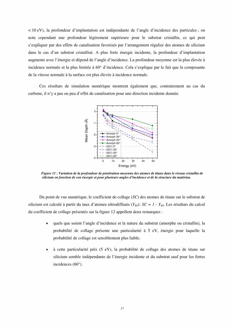
La figure 11 montre les variations de la profondeur de pénétration moyenne en fonction de
l’énergie des atomes incidents pour différents angles et natures de substrat. A faible énergie (typ.
0 5 10 15 20 250.0
0.1
0.2
0.3
0.4
0.5
0.6
0.7
0.8
0.9
1.0
1.1
1.2Sticking coefficients
Stic
king
coe
ffici
ent
Sputtered Ti atoms (x1014)
17
< 10 eV), la profondeur d’implantation est indépendante de l’angle d’incidence des particules ; on
note cependant une profondeur légèrement supérieure pour le substrat cristallin, ce qui peut
s’expliquer par des effets de canalisation favorisés par l’arrangement régulier des atomes de silicium
dans le cas d’un substrat cristallisé. A plus forte énergie incidente, la profondeur d’implantation
augmente avec l’énergie et dépend de l’angle d’incidence. La profondeur moyenne est la plus élevée à
incidence normale et la plus limitée à 60° d’incidence. Cela s’explique par le fait que la composante
de la vitesse normale à la surface est plus élevée à incidence normale.
Ces résultats de simulation numérique montrent également que, contrairement au cas du
carbone, il n’y a pas ou peu d’effet de canalisation pour une direction incidente donnée.
Figure 11 : Variation de la profondeur de pénétration moyenne des atomes de titane dans le réseau cristallin de silicium en fonction de son énergie et pour plusieurs angles d’incidence et de la structure du matériau.
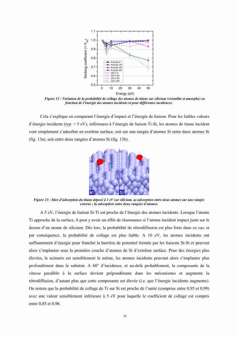
Du point de vue numérique, le coefficient de collage (SC) des atomes de titane sur le substrat de
silicium est calculé à partir du taux d’atomes rétrodiffusés (YBS): SC = 1 - YBS. Les résultats du calcul
du coefficient de collage présentés sur la figure 12 appellent deux remarques :
quels que soient l’angle d’incidence et la nature du substrat (amorphe ou cristallin), la
probabilité de collage présente une particularité à 5 eV, énergie pour laquelle la
probabilité de collage est sensiblement plus faible.
à cette particularité près (5 eV), la probabilité de collage des atomes de titane sur
silicium semble indépendante de l’énergie incidente et du substrat sauf pour les fortes
incidences (60°).
0 10 20 30 40 50-4
-3
-2
-1
0
Mea
n D
epth
(Å
)
Energy (eV)
Amorph 0° Amorph 30° Amorph 45° Amorph 60° (001) 0° (001) 30° (001) 45° (001) 60°
18
Figure 12 : Variation de la probabilité de collage des atomes de titane sur silicium (cristallin et amorphe) en
fonction de l’énergie des atomes incidents et pour différentes incidences.
Cela s’explique en comparant l’énergie d’impact et l’énergie de liaison. Pour les faibles valeurs
d’énergie incidente (typ. < η eV), inférieures à l’énergie de liaison Ti-Si, les atomes de titane incident
vont simplement s’adsorber en extrême surface, soit sur une rangée d’atomes Si entre deux atomes Si
(fig. 13a), soit entre deux rangées d’atomes Si (fig. 13b).
Figure 13 : Sites d’adsorption du titane déposé à 1 eV sur silicium. a) adsorption entre deux atomes sur une rangée
externe ; b) adsorption entre deux rangées d’atomes.
A η eV, l’énergie de liaison Si-Ti est proche de l’énergie des atomes incidents. Lorsque l’atome
Ti approche de la surface, il peut y avoir un effet de résonnance si l’atome incident impact juste sur le
dessus d’un atome de silicium. Dès lors, la probabilité de rétrodiffusion est plus forte dans ce cas, et
par conséquence, la probabilité de collage est plus faible. A 10 eV, les atomes incidents ont
suffisamment d’énergie pour franchir la barrière de potentiel formée par les liaisons Si-Si et peuvent
alors s’implanter sous la première couche d’atomes de Si d’extrême surface. Pour des énergies plus
élevées, le scénario est sensiblement le même, les atomes incidents pouvant alors s’implanter plus
profondément dans le substrat. A 60° d’incidence, et au-delà probablement, la composante de la
vitesse parallèle à la surface devient prépondérante dans les mécanismes et augmente la
rétrodiffusion, d’autant plus que cette composante est élevée (i.e. que l’énergie incidente augmente).
On notera que la probabilité de collage de Ti sur Si est proche de l’unité (comprise entre 0,9η et 0,99)
avec une valeur sensiblement inférieure à 5 eV pour laquelle le coefficient de collage est compris
entre 0,85 et 0,96.
0 10 20 30 40 500.5
0.6
0.7
0.8
0.9
1.0
1.1
Amorph 0° Amorph 30° Amorph 45° Amorph 60° (001) 0° (001) 30° (001) 45° (001) 60°
Stic
king
coe
ffici
ent (
1-Y
BS)
Energy (eV)
19
5 Dépôt de tungstène sur silicium
Comme dans le cas du dépôt de titane, des dépôts de tungstène ont été réalisés par pulvérisation
cathodique dans l’instrument storing matter avec des ions Ar+ de 10 keV. Les conditions de dépôt et
les procédures d’analyse sont similaires à celles utilisées dans le cas du titane. Toutefois, dans ce cas,
les mesures sont beaucoup plus sensibles aux effets de matrice qui conduisent à sous-estimer les
valeurs du coefficient de collage.
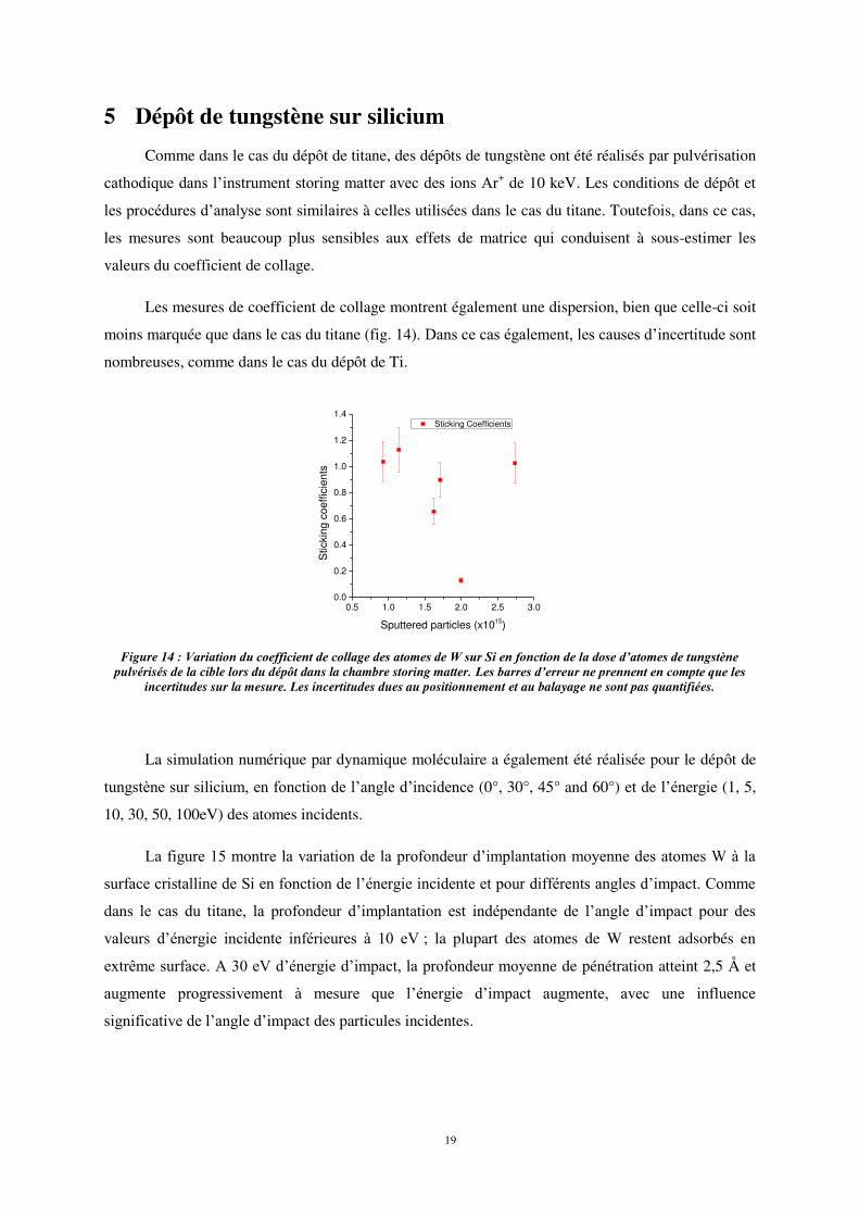
Les mesures de coefficient de collage montrent également une dispersion, bien que celle-ci soit
moins marquée que dans le cas du titane (fig. 14). Dans ce cas également, les causes d’incertitude sont
nombreuses, comme dans le cas du dépôt de Ti.
Figure 14 : Variation du coefficient de collage des atomes de W sur Si en fonction de la dose d’atomes de tungstène
pulvérisés de la cible lors du dépôt dans la chambre storing matter. Les barres d’erreur ne prennent en compte que les incertitudes sur la mesure. Les incertitudes dues au positionnement et au balayage ne sont pas quantifiées.
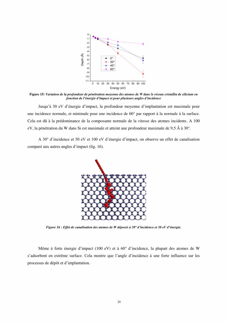
La simulation numérique par dynamique moléculaire a également été réalisée pour le dépôt de
tungstène sur silicium, en fonction de l’angle d’incidence (0°, 30°, 45° and 60°) et de l’énergie (1, 5,
10, 30, 50, 100eV) des atomes incidents.
La figure 1η montre la variation de la profondeur d’implantation moyenne des atomes W à la
surface cristalline de Si en fonction de l’énergie incidente et pour différents angles d’impact. Comme
dans le cas du titane, la profondeur d’implantation est indépendante de l’angle d’impact pour des
valeurs d’énergie incidente inférieures à 10 eV ; la plupart des atomes de W restent adsorbés en
extrême surface. A 30 eV d’énergie d’impact, la profondeur moyenne de pénétration atteint 2,5 Å et
augmente progressivement à mesure que l’énergie d’impact augmente, avec une influence
significative de l’angle d’impact des particules incidentes.
0.5 1.0 1.5 2.0 2.5 3.00.0
0.2
0.4
0.6
0.8
1.0
1.2
1.4 Sticking Coefficients
Stic
king
coe
ffici
ents
Sputtered particles (x1015)
20
Figure 15: Variation de la profondeur de pénétration moyenne des atomes de W dans le réseau cristallin de silicium en
fonction de l’énergie d’impact et pour plusieurs angles d’incidence
Jusqu’à 30 eV d’énergie d’impact, la profondeur moyenne d’implantation est maximale pour
une incidence normale, et minimale pour une incidence de 60° par rapport à la normale à la surface.
Cela est dû à la prédominance de la composante normale de la vitesse des atomes incidents. A 100
eV, la pénétration du W dans Si est maximale et atteint une profondeur maximale de 9,5 Å à 30°.
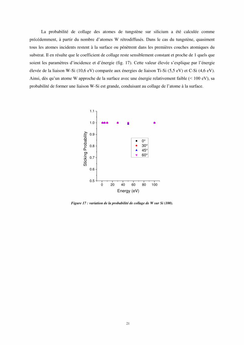
A 30° d’incidence et η0 eV et 100 eV d’énergie d’impact, on observe un effet de canalisation
comparé aux autres angles d’impact (fig. 16).
Figure 16 : Effet de canalisation des atomes de W déposés à 30° d’incidence et 30 eV d’énergie.
Même à forte énergie d’impact (100 eV) et à 60° d’incidence, la plupart des atomes de W
s’adsorbent en extrême surface. Cela montre que l’angle d’incidence à une forte influence sur les
processus de dépôt et d’implantation.
0 10 20 30 40 50 60 70 80 90 100-11
-10
-9
-8
-7
-6
-5
-4
-3
-2
-1
0
Dep
th (
Å)
Energy (eV)
0° 30° 45° 60°
21
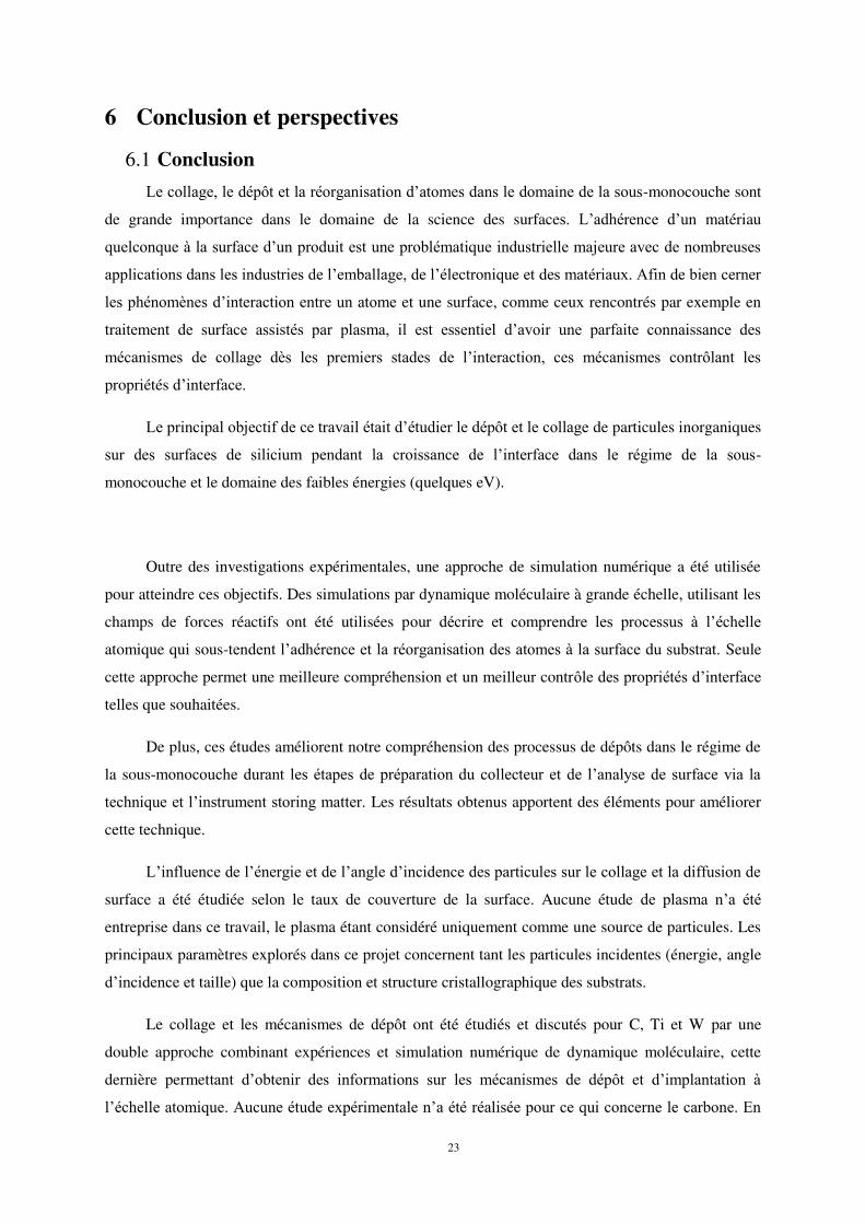
La probabilité de collage des atomes de tungstène sur silicium a été calculée comme
précédemment, à partir du nombre d’atomes W rétrodiffusés. Dans le cas du tungstène, quasiment
tous les atomes incidents restent à la surface ou pénètrent dans les premières couches atomiques du
substrat. Il en résulte que le coefficient de collage reste sensiblement constant et proche de 1 quels que
soient les paramètres d’incidence et d’énergie (fig. 17). Cette valeur élevée s’explique par l’énergie
élevée de la liaison W-Si (10,6 eV) comparée aux énergies de liaison Ti-Si (5,5 eV) et C-Si (4,6 eV).
Ainsi, dès qu’un atome W approche de la surface avec une énergie relativement faible (< 100 eV), sa
probabilité de former une liaison W-Si est grande, conduisant au collage de l’atome à la surface.
Figure 17 : variation de la probabilité de collage de W sur Si (100).
0 20 40 60 80 1000.5
0.6
0.7
0.8
0.9
1.0
1.1
0° 30° 45° 60°
Stic
king
Pro
babi
lity
Energy (eV)

22
23
6 Conclusion et perspectives
Conclusion 6.1
Le collage, le dépôt et la réorganisation d’atomes dans le domaine de la sous-monocouche sont
de grande importance dans le domaine de la science des surfaces. L’adhérence d’un matériau
quelconque à la surface d’un produit est une problématique industrielle majeure avec de nombreuses
applications dans les industries de l’emballage, de l’électronique et des matériaux. Afin de bien cerner
les phénomènes d’interaction entre un atome et une surface, comme ceux rencontrés par exemple en
traitement de surface assistés par plasma, il est essentiel d’avoir une parfaite connaissance des
mécanismes de collage dès les premiers stades de l’interaction, ces mécanismes contrôlant les
propriétés d’interface.
Le principal objectif de ce travail était d’étudier le dépôt et le collage de particules inorganiques
sur des surfaces de silicium pendant la croissance de l’interface dans le régime de la sous-
monocouche et le domaine des faibles énergies (quelques eV).
Outre des investigations expérimentales, une approche de simulation numérique a été utilisée
pour atteindre ces objectifs. Des simulations par dynamique moléculaire à grande échelle, utilisant les
champs de forces réactifs ont été utilisées pour décrire et comprendre les processus à l’échelle
atomique qui sous-tendent l’adhérence et la réorganisation des atomes à la surface du substrat. Seule
cette approche permet une meilleure compréhension et un meilleur contrôle des propriétés d’interface
telles que souhaitées.
De plus, ces études améliorent notre compréhension des processus de dépôts dans le régime de
la sous-monocouche durant les étapes de préparation du collecteur et de l’analyse de surface via la
technique et l’instrument storing matter. Les résultats obtenus apportent des éléments pour améliorer
cette technique.
L’influence de l’énergie et de l’angle d’incidence des particules sur le collage et la diffusion de
surface a été étudiée selon le taux de couverture de la surface. Aucune étude de plasma n’a été
entreprise dans ce travail, le plasma étant considéré uniquement comme une source de particules. Les
principaux paramètres explorés dans ce projet concernent tant les particules incidentes (énergie, angle
d’incidence et taille) que la composition et structure cristallographique des substrats.
Le collage et les mécanismes de dépôt ont été étudiés et discutés pour C, Ti et W par une
double approche combinant expériences et simulation numérique de dynamique moléculaire, cette
dernière permettant d’obtenir des informations sur les mécanismes de dépôt et d’implantation à
l’échelle atomique. Aucune étude expérimentale n’a été réalisée pour ce qui concerne le carbone. En
24
effet, notre système expérimental est tel que la contamination par le carbone ne peut pas être réduite à
un niveau où elle n’interférerait pas significativement avec les dépôts en régime de sous-monocouche.
En conséquence, des travaux de simulation supplémentaires ont été faits dans le cas du carbone, à
savoir l’étude de l’interaction d’un flux continu de carbone avec la surface.
Dans le cas du carbone, la simulation de dynamique moléculaire fournit des renseignements sur
l’interaction carbone silicium à faible énergie d’impact. Qu’il s’agisse d’un atome de carbone unique
ou d’un flux d’atomes, les simulations décrivent plusieurs aspects des mécanismes d’adhérence et
d’implantation. Le champ de force développé par John Kieffer a été choisi pour les simulations car il
permet de prendre en considération la formation et la rupture des liaisons atomiques via les transferts
de charge en fonction de l’environnement des atomes.
Les résultats pour l’interaction d’un atome C unique concernent les variations dela profondeur
moyenne de pénétration, la distribution en profondeur d’implantation, le ratio dépôt/implantation et la
probabilité de rétrodiffusion. Les résultats correspondants ont été validés par comparaison avec une
autre simulation faites en utilisant les potentiels bien établis de Erhart-Albe. Malgré quelques légères
divergences - pour des incidences rasantes et les énergies les plus élevées - entre les résultats issus des
deux modèles, l’accord entre les deux est plus que satisfaisant.
Ces études de dynamique moléculaire ont été étendues au cas de l’interaction d’atomes de
carbone en continu afin d’appréhender et de mieux cerner non seulement le dépôt et l’implantation de
carbone dans le silicium, mais également la formation de défauts et la réorganisation des atomes en
surface du substrat au cours de l’interaction d’atomes de faible énergie avec une surface de silicium
(100).
Les fonctions de distribution radiale et angulaire des atomes révèlent les modifications de la
structure Si-C selon l’énergie et l’angle d’incidence des particules, la dose d’atomes reçue et la
profondeur de pénétration dans le matériau. Il apparaît que la structure est fortement perturbée en
extrême surface alors qu’elle reste bien ordonnée à des profondeurs au-delà de 10 Å. Des conclusions
similaires peuvent être tirées des résultats portant sur les concentrations, la distribution en profondeur
ou encore les calculs de coordination. Il a été montré que l’énergie incidente des particules a plus
d’effet que l’angle d’incidence sur la réorganisation de surface du matériau.
L’analyse de résultats à différent étapes en faisant varier la dose d’atomes reçus fournit
également plusieurs aspects concernant les processus de dépôt et d’implantation. A 1 eV, des atomes
25
de carbone peuvent atteindre jusqu’à 1η Å de profondeur ce qui est principalement dû à des
mécanismes de diffusion.
Plusieurs aspects concernant le collage et l’adhérence du titane sur silicium ont fait l’objet d’un
chapitre dédié. Des résultats expérimentaux couplés à des simulations numériques ont permis
d’appréhender les mécanismes d’interaction d’atomes de titane avec une surface de silicium. Les
mécanismes aux interfaces durant le dépôt ont été discutés. Néanmoins, les investigations
expérimentales du coefficient de collage Ti sur Si n’ont pas montré de tendance particulière avec les
paramètres d’incidence. En revanche, les calculs de dynamique moléculaire ont conduit à des valeurs
de probabilité de collage comprises entre 0,8 et 0,99, et un effet de résonance a été mis en évidence
autour de η eV, qui conduit à une augmentation sensible du taux d’atomes rétrodiffusés, et diminution
en conséquence du coefficient de collage.
Une approche similaire a été réalisée dans le cas du dépôt d’atomes de tungstène sur silicium.
Les études expérimentales ont montré que les valeurs du coefficient de collage sont élevées, malgré
une certaine dispersion des résultats, cependant moindre que dans le cas du titane. Ces valeurs
expérimentales ont pu être corrélées aux résultats numériques avec un accord satisfaisant. Les valeurs
élevées de la probabilité de collage (proches de 1) sont probablement due à l’énergie élevée de la
liaison W-Si (10,6 eV), favorisant le collage d’atomes ayant une énergie d’impact modérée (< 100
eV). Plusieurs autres investigations ont pu être menées par dynamique moléculaire, concernant par
exemple le déplacement latéral des atomes ou encore l’implantation. En particulier, il a été montré
que lorsque le déplacement latéral est important, la profondeur de pénétration est faible et vice versa.
D’une manière générale, on peut conclure que ce travail apporte une contribution significative à
la description et la compréhension des mécanismes de collage et de dépôt de particules inorganiques
(C, Ti, W) dans le régime de la sous-monocouche.
Perspectives 6.2
Les coefficients de collage ont été déterminés par la technique couplée storing matter / SIMS.
Toutefois, il est nécessaire d’améliorer la précision des mesures, en particulier pour ce qui concerne le
positionnement du collecteur dans l’instrument stroring matter et son repérage dans l’analyseur SIMS.
De même, les problèmes de contamination rencontrés avec les outils expérimentaux utilisés
limitent les mesures expérimentales à quelques éléments. L’utilisation d’une chambre sous ultra vide
unique pour le dépôt et pour l’analyse permettrait de s’affranchir des contaminations (a minima de les
limiter).
26
Un autre aspect qui se doit d’être considéré concerne la couche d’oxyde natif inévitable qui se
forme à la surface du silicium, malgré les conditions d’ultravide utilisées pour nos dépôts
expérimentaux. En effet, cette couche d’oxyde n’est pas prise en compte dans les simulations
numériques qui considèrent une surface parfaitement propre et exempte de toute contamination ou
oxydation.
De même, les simulations sont réalisées avec des angles d’incidence parfaitement déterminés
alors que ceux-ci sont inconnus dans l’expérience, les atomes pulvérisés étant émis dans un certain
angle solide. Il en est de même pour ce qui concerne l’énergie des particules incidentes, bien fixée
dans les simulations numériques, mais distribuées sur une gamme d’énergie plus ou moins large dans
l’instrument storing matter.
Le dépôt de carbone a été étudié pour un atome unique et pour un flux d’atomes. Cette étude
pour plusieurs atomes doit également être réalisée pour ce qui concerne le titane et le tungstène. Cela
permettra d’avoir des points de comparaisons plus réalistes par rapport aux techniques de dépôt par
pulvérisation à faible énergie.
Ce travail est une première étape vers une description des mécanismes de dépôts de SiC, TiC et
WC, matériaux dont les applications sont nombreuses. Ainsi une prochaine étape pourrai être
d’étudier les mécanismes afférents à ces carbures.
Enfin, après avoir étudié l’interaction d’un atome (même en flux continu), il serait intéressant
de s’intéresser au comportement des particules et de la surface sous l’impact d’agrégats d’atomes au
lieu d’atomes isolés.
Plusieurs autres aspects enfin pourraient être étudiés tels que la formation d’îlots, la diffusion
lors de l’analyse, etc. ; cela apporterait des renseignements quant aux processus fondamentaux
impliqués dans les processus d’émission d’ions secondaires

27
Collage et adhérence de particules dans le domaine de la sous-monocouche Résumé
Au cours d’un traitement de surface de type dépôt assisté par plasma, les caractéristiques et propriétés de l’interface entre le dépôt et le substrat sont déterminées par la première couche atomique du dépôt, voire les premiers atomes qui commencent à recouvrir la surface du substrat. Aussi, la parfaite connaissance du comportement des particules incidentes et du réarrangement des atomes suite à l’impact d’une particule du plasma est-elle un élément essentiel à la description du comportement de la surface en cours de traitement et donc de ses propriétés ultérieures. Au cours de cette thèse, nous avons entrepris d’étudier, par une approche combinant expériences et simulation numérique par dynamique moléculaire, l’interaction d’espèces (C, Ti, W) avec une surface de silicium en fonction de paramètres tels que l’énergie, la fluence ou encore l’incidence des particules arrivant sur la surface. Une part importante de ce travail a consisté à adapter les codes de dynamique moléculaire (utilisation des champs de force réactifs) aux systèmes étudiés. La partie expérimentale a nécessité la mise en place de procédures spécifiques pour l’utilisation de l’équipement Storing Matter. Les résultats montrent que, quelle que soit l’espèce incidente, parmi celles étudiées, le coefficient de collage (SC) est dans la gamme [0.7 – 1] ; dans le cas de W, quasiment tous les atomes incidents restent sur la
surface (SC1). Outre la détermination du coefficient de collage, pour différentes conditions initiales des espèces incidentes (énergie, incidence, fluence) les modifications apportées à la surface ont également été déterminées en termes d’implantation et de trajectoire dans le matériau des espèces incidentes, et de pulvérisation de la surface du substrat.
Mots-Clés : Dynamique moléculaire, coefficient de collage, SIMS, Storing Matter, sous-monocouche.
Sticking and deposition of atoms in the sub-monolayer range Abstract
During plasma assisted deposition, properties of the coating substrate interface depend on the first atomic layer of the deposit, or the atoms that first start to cover the surface. Therefore the good knowledge of the sticking coefficient and the reorganization of the surface following particle impact is an essential issue to achieve the description of the behavior of the processed surface and, therefore, its expected properties. Consequently, we investigated the interaction between incoming particles (C, Ti, W) and a silicon surface by using an approach combining molecular dynamic simulations and experiments. Various initial conditions were studied, energy, fluence and incidence angle of the incoming particles. An important part of this work has consisted in adapting the molecular dynamic codes (using reactive force fields) to the investigated systems. Meanwhile, experimental procedure specifically devoted to the use of the Storing Matter facility was also developed. Results show that the sticking coefficient (SC) value is in the range [0.7 – 1] irrespectively of the incoming species; in the
case of W, almost all atoms stick on the surface (SC1). Besides the determination of sticking coefficient, the surface modification resulting from the particles impingement were determined for various initial conditions (energy, fluence, angle) in terms of implantation and displacement of the incoming species, and surface sputtering as well.
Keywords: Molecular dynamic simulations, sticking coefficient, SIMS, Storing matter, Sub monolayer.
UNIVERSITE DE LORRAINE
Ecole Doctorale : Énergie Mécanique Matériaux
Institut Jean Lamour Département Chimie et Physique des Solides et des Surfaces
THESIS
defended on 18/07/2014
to obtain the degree of Doctor of the University of Lorraine
in material science and engineering
by
Arindam JANA
Sticking and deposition of atoms in the sub-monolayer range.
Jury
President: Mohammed BELMAHI Professor, University of Lorraine Reviewers: Laurent HOUSSIAU Professor, University of Namur, Belgium. Pascal BRAULT Senior researcher (DR) CNRS, GREMI, University of Orléans. Examiners: Kai NORDLUND Professor, University of Helsinki, Finland. Supervisors : Gérard HENRION Senior researcher (DR) CNRS, IJL, University of Lorraine Patrick PHILIPP Project leader, CRP Gabriel Lippmann, Belvaux, Luxembourg.

2

3
*Dedicated to my parents and my family*

4

5
Acknowledgements
After working for more than three and half years in a PhD research, I would compare this experience
to a maze in where colleagues and other professionals as well as friends and family, are posted in
many intersections to guide you through many corridors and towards the exit. With this thesis, I
finally managed to get out of this maze and I would like, now, to thank all the people who made me
follow the path I used.
First, I wish to express my hearty gratitude to Dr. Tow Wirtz and Dr. Patrick Philipp who believed in
me by accepting me within their team at UIS group. I am really grateful to Dr. Patrick Philipp for his
constant guidance and his constructive attitude, which was always driving me to go further. I would
like to express my hearty gratitude and many thanks to Dr. Gérard Henrion for his constant support
and valuable guidance. Without his comments and modifications, the thesis would never have been
the same. I am grateful as well to Prof. Laurent Houssiau and Dr. Pascal Brault who accepted to be
my reviewer, and for their strong commitment in reading my thesis. I also wish to express my
gratitude to Prof. Kai Nordlund and Prof. Mohammed Belmahi to make time and be part of my
defense committee.
This work was financially supported by Fonds National de la Recherche, Luxembourg (FNR) by
means of an AFR grant (grant number: PHD-MARP-05) and without their money, this thesis would
not exist, so: thank you.
I really appreciate the help of Dr. Ludovic Briquet who constantly guided me through the puzzle of
computation since my first day at UIS group. Also I would like to express many thanks to Dr. Jean
Nicolas Audinot and Brahime Eladib for their constant help while I was working in dynamic SIMS. I
am also really grateful to Samir Menaouli, Arnaud Moschetta, and Alain Robert for their efficient
engineering support and valuable technical assistance whenever it was required.
I am also very grateful to Ben, Canan, David, Hung, Ioana, Lukasz, Olivier de Castro, Olivier Bouton
Mathieu, Marina, Nimer, Rachid, Roch, Santhana and Yves for their precious suggestions, refreshing
discussions, and pleasant humours. I would like to thank other actual or former colleagues of UIS
group, with whom I shared so many outings, leisure times as well as many discussions regarding how
to solve biggest problems of the world. I really had a good time while sharing those discussions with
so many cultures and different opinions within the whole SAM.
I also would like to express my gratitude and thanks to all those whose names are not mentioned here
but who provided support of personal, scientific, technical, or in administrative nature.

6
7
Table of contents
CHAPITRE 0. GENERAL SCOPE AND CONTENT OF THE THESIS ...................................................................... 9
CHAPITRE 1. STATE OF THE ART ............................................................................................................... 13
1) INTRODUCTION ................................................................................................................................................. 13
2) MOLECULAR DYNAMICS SIMULATIONS: A LITERATURE REVIEW.................................................................................... 13
i) Introduction .............................................................................................................................................. 13
ii) The choice of the appropriate force field ................................................................................................. 15
iii) MD studies on epitaxial growth, reaction mechanisms and adhesion .................................................... 17
iv) MD studies on angle dependence ........................................................................................................... 20
v) MD studies on film microstructure ........................................................................................................... 21
3) PLASMA TREATMENT .......................................................................................................................................... 22
i) Introduction .............................................................................................................................................. 22
4) SECONDARY ION MASS SPECTROSCOPY AND SPUTTERING PROCESSES .......................................................................... 25
i) SIMS analysis for inorganic materials ....................................................................................................... 25
ii) Sputtering by ion/particle bombardment ................................................................................................ 25
iii) Angular distributions of the emitted particles: ....................................................................................... 27
5) THE STORING MATTER TECHNIQUE ....................................................................................................................... 29
CHAPITRE 2. TECHNIQUES AND CONDITIONS ............................................................................................ 35
1) INTRODUCTION ................................................................................................................................................. 35
2) SIMULATION TECHNIQUES ................................................................................................................................... 35
i) Simulation conditions for single C, Ti and W depositions on Si(100) ........................................................ 40
ii) Simulation conditions for multiple impacts of C on Si (100) ..................................................................... 44
3) EXPERIMENTAL TECHNIQUES ................................................................................................................................ 44
i) Storing matter technique: principle and instrumental description ........................................................... 44
ii) Secondary Ion Mass Spectroscopy: Instrumental description .................................................................. 48
CHAPITRE 3. CARBON (C) DEPOSITION ON SI (100) BY MOLECULAR DYNAMICS SIMULATIONS ................. 57
1) INTRODUCTION : ............................................................................................................................................... 57
2) SECTION 1: RESULTS FOR SINGLE CARBON DEPOSITION .............................................................................................. 58
i) Deposition, Implantation and Backscattering of carbon atoms. .............................................................. 58
ii) Implantation of the carbon atoms. .......................................................................................................... 60
iii) Comparison with DFT. ............................................................................................................................. 64
iv) Sticking coefficient .................................................................................................................................. 65
8
v) Conclusion and outlook ............................................................................................................................ 66
3) SECTION 2: RESULTS FOR CONTINUOUS CARBON DEPOSITION.................................................................................... 67
i) Introduction .............................................................................................................................................. 67
ii) Results and discussion .............................................................................................................................. 67
iii) Results for multiple carbons at constant energy ..................................................................................... 68
iv) Results for continuous C deposition at constant angle for different energies......................................... 72
v) Evolution of the system with deposition dose .......................................................................................... 79
4) CONCLUSION .................................................................................................................................................... 87
CHAPITRE 4. TITANIUM (TI) DEPOSITION ON SILICON (SI) ......................................................................... 91
1) INTRODUCTION: ................................................................................................................................................ 91
2) EXPERIMENTAL SETUP AND CONDITIONS................................................................................................................. 91
i) Collector (Si) and Target (Ti) preparation process .................................................................................... 91
ii) Storing matter set up and conditions ....................................................................................................... 92
iii) Analysis conditions in SIMS ..................................................................................................................... 92
3) RESULTS AND DISCUSSION: EXPERIMENTAL ............................................................................................................. 94
i) Depth profile of a Ti deposit: ..................................................................................................................... 94
ii) Characterisation of the sub-monolayer deposits ..................................................................................... 95
4) SIMULATION RESULTS: ...................................................................................................................................... 104
5) CONCLUSIONS: ............................................................................................................................................... 108
CHAPITRE 5. TUNGSTEN (W) DEPOSITION ON SILICON (SI) ...................................................................... 113
1) INTRODUCTION: .............................................................................................................................................. 113
2) EXPERIMENTAL SETUP ...................................................................................................................................... 113
i) Storing matter conditions for W deposits ............................................................................................... 113
ii) Analysis conditions in SIMS .................................................................................................................... 114
3) RESULTS AND DISCUSSION ................................................................................................................................. 114
i) Depth Profile of a W deposit: .................................................................................................................. 114
ii) Characterisation of the sub-monolayer deposits ................................................................................... 115
4) SIMULATION RESULTS: ...................................................................................................................................... 120
5) CONCLUSIONS: ............................................................................................................................................... 127
CHAPITRE 6. CONCLUSION AND OUTLOOK .............................................................................................. 131
1) CONCLUSION .................................................................................................................................................. 131
2) OUTLOOK ...................................................................................................................................................... 133
REFERENCES ................................................................................................................................................. 137
9
Chapitre 0.
General scope and content of the thesis
The investigation of sticking, deposition and reorganization of atoms or molecules in the sub-
monolayer range has a great importance in the surface treatment field, where the first monolayer
describes the interface characteristics and structure between substrate and deposited layer as well as
the adhesion properties of this deposited layer on the substrate surface. The properties of the interface
are of great significance as interface is often the site where fracture of multi-layered systems
originates.
In order to well understand the interactions between atoms and surfaces, as could be the case in
plasma surface treatments, it is essential to get a perfect knowledge on the sticking mechanisms
during the early stage of growth since these mechanisms control the interface properties. Therefore
deposition mechanisms are fundamental in understanding how the atomic interactions influence the
interface properties. At the same time understanding of atomic scale behavior during sub-monolayer
or monolayer growth is also fundamental for basic and applied problems of surface science.
In this work, plasmas are not investigated by themselves but this work brings more fundamental
understanding on the interaction of few-eV energy atoms, i.e. energies similar to those found in
plasmas.At the same time, sputter deposition process is a very attractive well established technique for
the formation of metal thin films and it has lots of applications in various fields of interest like
electronic, optical, medical, and automobile industries. A reproducible realization of a good adhesion
and sticking of any material to a product surface is an important industrial problem with many
applications like decoration of plates, integrated circuits, photoconductive materials, protection from
corrosion, abrasion or thermal resistance. Sticking and adhesion then, is important as soon as one
wants to combine homogeneous or heterogeneous materials together without help of any mechanical
fixation.
The main objective of this PhD work is to better investigate and understand the deposition, sticking
and reorganization behaviour of inorganic particles on silicon surfaces during the growth of interface
in sub monolayer range at low energies, i.e. energies found in magnetron sputtering and similar
plasma deposition techniques and how some parameters (angle, energy, dose) influence the
deposition, implantation and interface properties. To attain these objectives, a multidisciplinary
approach involving, experimental investigations and numerical simulations have been incorporated to
10
investigate the sticking and deposition mechanism of atoms during the sub-monolayer growth in order
to obtain detailed description of the atomistic-scale mechanisms controlling the deposition of the very
first monolayers in particle-surface treatments. Large-scale MD simulations based on first-principle
reactive force fields are utilized to describe and understand the atomistic behaviour underlying the
reorganization and adhesion of atoms on the substrates. In this way, a better comprehension and
control of tailor-designed surface characteristics can be achieved. In addition, these studies will
contribute towards a better understanding of the deposition process in the sub-monolayer range during
the deposit preparation for the promising and new surface analysis technique “Storing Matter”. The
results achieved during this PhD work contribute to further enhance of this technique in terms of
sensitivity and quantification. The sticking properties and surface diffusion have been investigated for
different surfaces with respect to surface coverage varying the incidence angle and incident energy of
the atoms. In addition to MD simulations, sputter deposition technique (storing matter instrument) is
utilized to deposit matter in the sub-monolayer range. At the same time, secondary ion mass
spectroscopy has been used to characterize the deposits and to estimate the total amount of matter
deposited. Although plasma by itself is not studied in this project but it is consideredas a source of
atoms. The crucial parameters studied in this project comprise the particle properties (such as energy
and angular distributions) along with substrate composition and roughness.
In the first chapter, a general introduction to MD simulations, plasma treatments, SIMS and the
storing matter technique as well as literature studies regarding projects of interest are provided.
The second chapter deals with the details of simulation and experimental conditions along with MD
force field and instrumental descriptions.
The third chapter presents several sticking and deposition aspects of carbon on silicon (100). The first
section of this chapter deals with single carbon deposition followed by continuous carbon deposition
on silicon in the second part.
The fourth chapter describes the sticking behaviour of Ti on a silicon surface by sputter deposition
technique and also validated by MD simulation results.
The fifth and final chapter consists of sticking and deposition of tungsten on silicon surface done by
both MD simulation and storing matter combined with SIMS techniques.
11
State of Art
“Sticking and deposition during the initial stages of growth of
any material to a product surface is an important industrial
problem with many applications. A molecular dynamics
simulation along with plasma deposition technique has been
integral part of this work. A literature review related to this work
has been presented in this chapter.”

12
13
Chapitre 1.
State of the art
1) Introduction In this chapter existing literature studies related to fundamentals of the SubML project will be
presented. There will be four sections for the literature studies, which will complete the main
overview of the thesis. These four sections will consist of literature studies of molecular dynamics
simulations, plasma treatment, secondary ion mass spectroscopy and storing matter deposition
technique. In the molecular dynamics (MD) simulation section, we described past literature studies on
growth mechanism, microstructure, epitaxial growth, angle and energy dependence, etc. During the
deposition, examples of compound materials which may form include SiC, TiSi, WSi etc. So, in this
section we describe an overview of the different properties, characteristics and applications of these
materials and a comparison with past literature review. Special attention will be given to the different
parameters affecting the deposition mechanism at atomic scale.
2) Molecular Dynamics simulations: a literature review
i) Introduction
SubML project is executed in a multidisciplinary approach and MD simulation is one of the major
approaches used to reach the objectives of the project. Before describing literature studies on MD
simulations, we will have a look into several other simulation techniques, their use and why MD
simulations are most suitable for the SubML project. Several simulation techniques exist to
investigate plasma deposition processes. They include kinetic models, fluid models, Monte Carlo,
particle-in-cell Monte Carlo collision simulations and MD simulations. Depending on the phenomena
and the parameters to be investigated, the one or other technique is better suited. Fluid models are
used to study the discharge and to understand the complex and coupled interactions and how they are
affected by the design of the experimental setup and the operation conditions 1,2. Kinetic models are
used in a diversity of physico-chemical areas in which kinetic measurement provide significant
physical insight 3. Particle-in-cell simulations are widely used for the application to partially ionized
gases. They have the advantage of providing kinetic information such as velocities of the species in
the plasma 4,5. Plasma–surface interactions are best described by Monte Carlo (MC) and MD
simulations 6. Examples for the MC method include among other studies on the discharge 7,8. MD
studies report on the sticking on surfaces 9, the growth of diamond carbon films 10 and others.
14
Computer simulations in surface science have grown rapidly during the past decades. Modelling with
molecular dynamics simulation is considered as a beneficial complementary technique to several
experimental approaches as it explores detailed understanding of chemical and physical processes at
atomic and molecular level where the system properties can be controlled precisely and according to
wish. The analytical results and the understanding from MD simulation are as valuable as
experimental technique and can give a detailed insight into the phenomena when only limited
information can be obtained from experimental conditions. In the molecular dynamics simulation of
film deposition, an interatomic potential model is used and from the beginning of the simulations the
system is then followed by Newtonian physics as the time progresses. Incoming atoms impinging the
surface can be added to the system and the trajectories of atoms of the system can be followed till the
system relaxes. In general, the processes occurring during the MD simulations vastly depend on the
accuracy of the interatomic potentials which means that the latter need careful adjustment. The direct
effect of energy of incident atoms on film structures can be achieved by MD simulation analysis. The
results after the collisions give insights into atomic scale mechanism of low-energy many-body
collisions during the thin film growth 11,12. While dealing with low impact energies, MD simulations
are the best suitable method as they produce a fully deterministic description of the studied system
over short periods of time. The interactions between all the deposited atoms and the neighbouring
atoms are thoroughly considered, which is very important because the projectiles with such low
velocities experience the neighbouring chemical environment. During molecular dynamics
simulations, atom trajectories can be traced, which is a great interest for particle surface interactions.
As numerical simulation is one of the major parts of the project, we will focus now on papers
involving Monte Carlo (MC), Kinetic Monte Carlo (KMC), Density Functional Theory (DFT) and
also MD simulations. Gleason et al. did a study on the growth of hydrogenated Si from SiH3 and SiH2
radicals (derived from silane) while choosing the location of impacts of the precursor on the surface
arbitrarily 13. They observed that the state of the final film is mainly determined by the surface
diffusion of silicon containing species. McCaughey et al. did other investigations on the bulk and
surface characteristics of amorphous hydrogenated Si deposition from silane plasmas 14. They
concluded that the physical characteristics of the film mainly are determined by the relative fraction of
the radicals in the incident flux as well as the rate at which the radicals arrive on the surface. They
also observed that the roughness of the films mainly rely on the sticking coefficients of the incident
radicals as well as on the deposition rate to a lesser extent 14. Several current studies involve DFT
calculations, MD simulations, or KMC simulations or a combination of them. Ohira et al. performed
MD simulations studies with a many-body semi-classical potential to observe the basic processes
regarding microcrystalline silicon deposition with SiH4 diluted by H2 in a plasma enhanced chemical
vapour deposition (PECVD) 15. They observed the processes of crystallization of SiH3 radicals, the
processes of hydrogen desorption and Si structure stability at 500K substrate temperature. Bakos et
15
al. performed DFT calculations to understand pathways of reaction for the SiH3 radical with Si as a
function of the temperature and proved that SiH3 inserted into strained Si-Si bonds is free of barrier 16. They justified those results by MD simulation studies. In another paper, the aforesaid authors did
studies on the formation of disilane and its responses with the sample surface by using the similar
techniques 17. Pandey et al. performed KMC simulations as well as DFT calculations and studied
several surface kinetic events ( radical-surface diffusion, surface hydride dissociation reactions,
radical surface and adsorbed radical-radical interactions) to investigate the growth processes of
amorphous silicon as a function of the substrate temperature 18. Valipa et al. performed MD
simulations along with DFT calculations to understand the surface smoothening processes in
hydrogenated amorphous Si thin film deposition 19. Gordiets et al. described a kinetic model to
explain the process of thin film growth for films consisting of two components, like for example H
terminated Si films 20. Molecular dynamics studies regarding other materials involve surface
migration and adsorption processes on -Al2O3 by DFT calculations 21, sputtering and deposition on a
polystyrene surface by CF3+ and C3F5
+ ions 22, the 3D distributions of sputtered and scattered products
from Cu+ and Ar+ ion bombardment on Cu 23 or the energetic fluorine etching of SiC 24. Other
materials, which have been investigated by simulations involved diamond growth 25-27 or film growth
of hydrocarbon on SiC 28.
For any molecular dynamics calculation, molecular mechanics force field is the most important form.
It defines the forces between the particles in the system and the potential energy can be derived from
the forces. If the force field is known for a system, successively momentum, acceleration, velocity and
finally position of the particles can be deduced and determined.
ii) The choice of the appropriate force field
Force fields used during MD simulation studies are mostly classical force fields, where interactions
depend only on the interacting elements and on interatomic distance. At the same time, interactions
during such MD simulations are independent of chemical environment. The description of the plasma-
surface interactions needs information on the deposition and reorganization of particles at a sample
surface and also information of the particle energy and angle, as well as backscattering and etching.
Therefore, it is necessary to consider the formation and breaking of bonds while doing MD
simulations. Reactive force fields that include coulomb interactions with adjustable transfer of partial
charges and environment-dependent covalent bonding are better suited than classical force fields
(coulomb interactions with fix charges, or 2-body and 3-body interactions which do not depend on the
chemical environment) to observe systems going under structural change. There are several such force
fields which have been developed for different materials.
In recent years there has been a significant increment of interest for carbon film growth by low energy
carbon plasma and ion beam deposition. Several experimental studies of carbon film growth provide
16
important data of surface structure, bonding state and properties of the film deposited by different
techniques. MD simulation is one of the methods to understand atomic scale mechanism to get details
of the structural descriptions. Pailthorpe et al. developed a Stillinger-Weber (SW) 29 class of
interatomic potential for the modelling of both sp2 and sp3 interactions in diamond like carbon 30.
They actually derived the potential from Hartree-Fock calculations for small carbon clusters in
tetrahedral and trigonal configurations. The model has been applied for bulk diamond, carbon clusters
and thin film forms of high density amorphous carbon. The SW potential is an empirical inter-atomic
potential which was originally developed for silicon and is a sum over physically intuitive two body
bond stretching and three body bond bending interactions 29. This potential has been applied
successfully to the study of bulk and surface properties of silicon, to the sputtering of silicon surfaces,
to small silicon clusters and to bulk germanium 31-34.
Another interatomic potential developed by Tersoff 35,36,36, which includes the effects of coordination
number to improve the description of silicon clusters and surfaces, has been successfully used to
simulate the growth of amorphous carbon, and has been extended by Brenner to study carbon film
growth from hydrocarbon species 27. The REBO potential second-generation reactive empirical bond
order potential energy, originally evolves from the Brenner potential and has been extended for
hydrocarbon molecules and solid carbon 37. It enables covalent bond breaking and formation with
related changes in atomic hybridization based on a classical potential. This is related to the Abell-
Tersoff bond order potential 38 which has already been utilized in preceding version of this potential 27. Afterwards, this potential has been modified to incorporate oxygen, i.e. H-O, C-O and O-O bonds
to the already presented C-C, C-H and H-H bonds 39. This potential has been employed to the
investigation of the chemical stability and structure of various polymer chains and molecules and to
the modelling of chemical interactions within a series of molecules inside the limits of classical MD
simulations 39-45.
Another reactive force field associating hydrocarbons has been derived by van Duin et al. 46. The
ReaxFF force field utilizes a general association between bond order and bond distance on one hand
and between bond energy and bond order on the other hand which guides to proper dissociation of
bonds to discrete atoms. In addition to the Brenner potential 27, it involves Coulomb and van der
Waals interactions with a formerly developed approach to estimate charge distributions in molecules 47. The charges within the system are permitted to evolve dynamically with the modification of atomic
environment. The reaction and dissociation curves are obtained from quantum chemistry
computations 46. The force field developed has been continued to various systems, including silicon
oxide and silicon 48,49, hydride of magnesium50, materials with ferroelectric properties 51, platinum 52,
nickel 53, gold 54 and to catalytic reactions 55-57. This potential has been developed to include full
chemistry of the breaking and formation of bonds, in addition to a proper description of the fully
bound equilibrium geometry of complex molecules. However, its charge-equilibrium method, which
17
needs significantly larger computational efforts than classical force fields, limits the use of this force
field to relatively small systems. Yu et al. 58,59 described a charge optimized many-body (COMB)
potential for the Si/SiO2 system, which is based on the modified Tersoff potential described by
Yasukawa 60 to reduce the drawbacks of the ReaxFF potential (vast computational resources), and yet
produce correct results for the Si/SiO2 system. The effect of charge transfer is accounted by the many-
body interactions and electronegativity equalization principle.
There is another reactive force field which is developed by Kieffer et al. at the University of Michigan 61,62. This potential involves Coulomb interactions, directional covalent bonds, a torsion term and van
der Waals interactions. Important traits regarding this force field during simulating of systems which
undergo substantial structural changes are (i) the capability to consider for the redistribution of
density of electrons upon formation, ionization, or breaking of bonds, within a charge transfer term,
and (ii) the characteristics that the change in the coordination number of an atom arises because of
dynamical angular constraints.
In fact, the potential by Kieffer et al. was originated and successfully applied for inorganic materials 61,63-68,68,69. Within the Kieffer potential, a large number of silica polymorphs, including - and -
quartz , - and -cristobalite, stishovite, X-I silica, high-stishovite, and amorphous silica can be
computed with a single parameterization demonstrates to the transferability of the potential 62. Later
on, the force field was adjusted for the computation of polyamorphic transitions in vitreous B2O3
under pressure 65 and polyhedral oligomeric silsesquioxane POSS nano-assemblies 70 multiscale
simulations have been studied.
iii) MD studies on epitaxial growth, reaction mechanisms and adhesion
Several studies are done to observe how the energy affects the atomic scale mechanism during the
film deposition. For example during the deposition of silver atoms on a Ag(111) substrate, it was
found that increasing the energy of the depositing Ag atoms from 0.1 to 10 eV altered the film growth
mechanism from an island-growth mode toward a layer-by-layer mode71. The primary mechanism for
the redistribution of deposited atoms was found to be the collapse of unstable clusters for the 0.1 eV
deposition and displacements of surface atoms by ballistic collisions at 10 eV71. For energies of l0, 20
and 40 eV, further simulations showed that an interface mixing phenomenon occurred via an atom
exchange mechanism at the surface. The mechanism of this surface exchange was activated by
ballistic collisions, but was also assisted by thermal vibrations of the substrate lattice 72. Epitaxial
growth can be achieved by using the energetic atoms for depositions 73. Some studies by molecular
dynamics simulations have been done also at different temperatures to observe the temperature
influence on growth mechanisms. J. Tarus and K. Nordlund did a molecular dynamics simulation
study on Si20 cluster deposition on Si(001) at two different temperatures (300K and 1000K) 74. They
found a significant change in epitaxial growth at 1000K but they did not find any kind of epitaxial
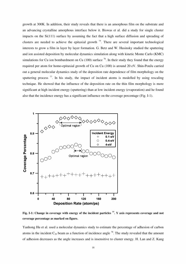
18
growth at 300K. In addition, their study reveals that there is an amorphous film on the substrate and
an advancing crystalline amorphous interface below it. Biswas et al. did a study for single cluster
impacts on the Si(111) surface by assuming the fact that a high surface diffusion and spreading of
clusters are needed to achieve the epitaxial growth 75. There are several important technological
interests to grow a film in layer by layer formation. G. Betz and W. Husinsky studied the sputtering
and ion assisted deposition by molecular dynamics simulation along with kinetic Monte Carlo (KMC)
simulations for Cu ion bombardment on Cu (100) surface 76. In their study they found that the energy
required per atom for homo-epitaxial growth of Cu on Cu (100) is around 20 eV. Shin-PonJu carried
out a general molecular dynamics study of the deposition rate dependence of film morphology on the
sputtering process 77. In his study, the impact of incident atoms is modelled by using rescaling
technique. He showed that the influence of the deposition rate on the thin film morphology is more
significant at high incident energy (sputtering) than at low incident energy (evaporation) and he found
also that the incidence energy has a significant influence on the coverage percentage (Fig. I-1).
Fig. I-1: Change in coverage with energy of the incident particles 77. Y axis represents coverage and not
coverage percentage as marked on figure.
Yanhong Hu et al. used a molecular dynamics study to estimate the percentage of adhesion of carbon
atoms in the incident C20 beam as a function of incidence angle 78. The study revealed that the amount
of adhesion decreases as the angle increases and is insensitive to cluster energy. H. Lan and Z. Kang
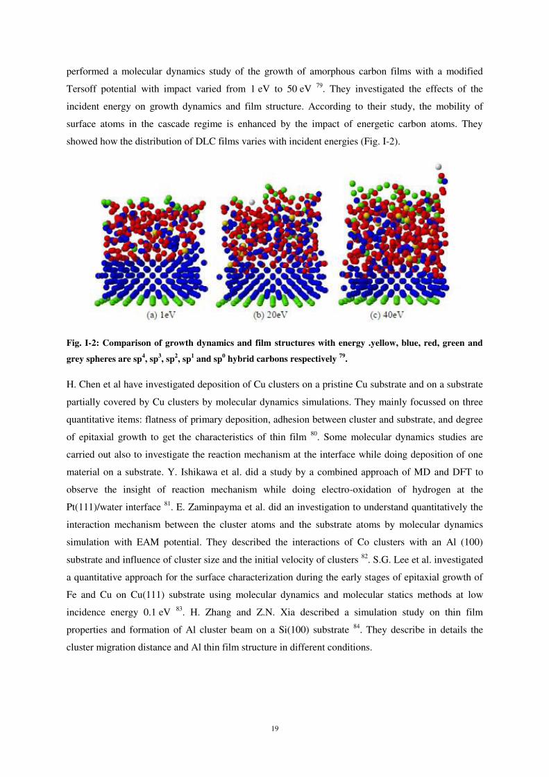
19
performed a molecular dynamics study of the growth of amorphous carbon films with a modified
Tersoff potential with impact varied from 1 eV to 50 eV 79. They investigated the effects of the
incident energy on growth dynamics and film structure. According to their study, the mobility of
surface atoms in the cascade regime is enhanced by the impact of energetic carbon atoms. They
showed how the distribution of DLC films varies with incident energies (Fig. I-2).
Fig. I-2: Comparison of growth dynamics and film structures with energy .yellow, blue, red, green and
grey spheres are sp4, sp3, sp2, sp1 and sp0 hybrid carbons respectively 79.
H. Chen et al have investigated deposition of Cu clusters on a pristine Cu substrate and on a substrate
partially covered by Cu clusters by molecular dynamics simulations. They mainly focussed on three
quantitative items: flatness of primary deposition, adhesion between cluster and substrate, and degree
of epitaxial growth to get the characteristics of thin film 80. Some molecular dynamics studies are
carried out also to investigate the reaction mechanism at the interface while doing deposition of one
material on a substrate. Y. Ishikawa et al. did a study by a combined approach of MD and DFT to
observe the insight of reaction mechanism while doing electro-oxidation of hydrogen at the
Pt(111)/water interface 81. E. Zaminpayma et al. did an investigation to understand quantitatively the
interaction mechanism between the cluster atoms and the substrate atoms by molecular dynamics
simulation with EAM potential. They described the interactions of Co clusters with an Al (100)
substrate and influence of cluster size and the initial velocity of clusters 82. S.G. Lee et al. investigated
a quantitative approach for the surface characterization during the early stages of epitaxial growth of
Fe and Cu on Cu(111) substrate using molecular dynamics and molecular statics methods at low
incidence energy 0.1 eV 83. H. Zhang and Z.N. Xia described a simulation study on thin film
properties and formation of Al cluster beam on a Si(100) substrate 84. They describe in details the
cluster migration distance and Al thin film structure in different conditions.
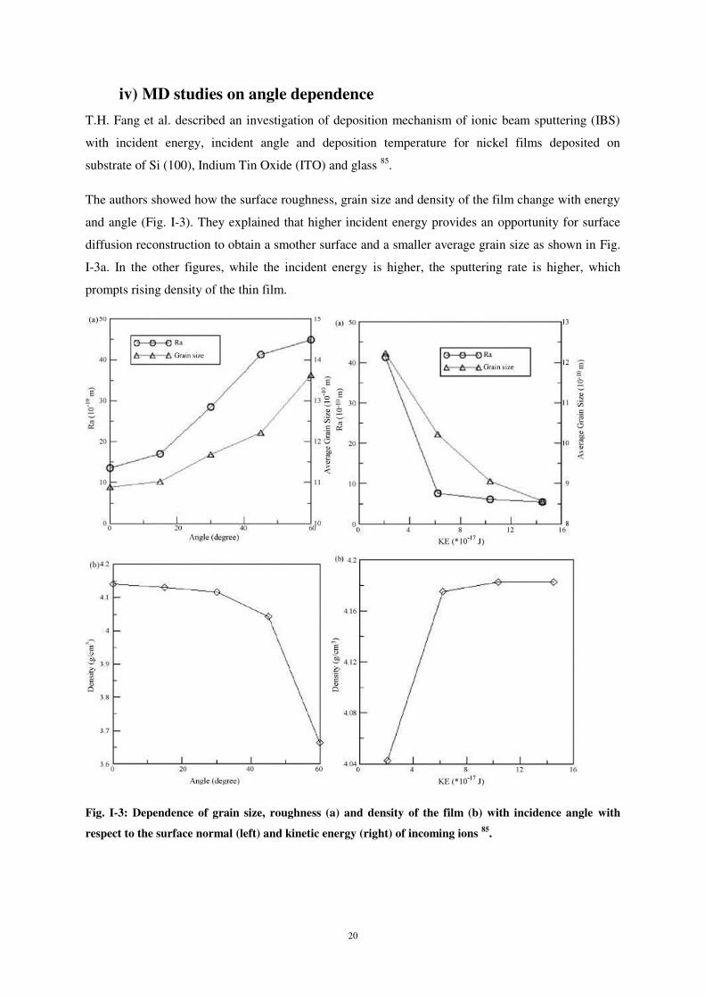
20
iv) MD studies on angle dependence
T.H. Fang et al. described an investigation of deposition mechanism of ionic beam sputtering (IBS)
with incident energy, incident angle and deposition temperature for nickel films deposited on
substrate of Si (100), Indium Tin Oxide (ITO) and glass 85.
The authors showed how the surface roughness, grain size and density of the film change with energy
and angle (Fig. I-3). They explained that higher incident energy provides an opportunity for surface
diffusion reconstruction to obtain a smother surface and a smaller average grain size as shown in Fig.
I-3a. In the other figures, while the incident energy is higher, the sputtering rate is higher, which
prompts rising density of the thin film.
Fig. I-3: Dependence of grain size, roughness (a) and density of the film (b) with incidence angle with
respect to the surface normal (left) and kinetic energy (right) of incoming ions 85.
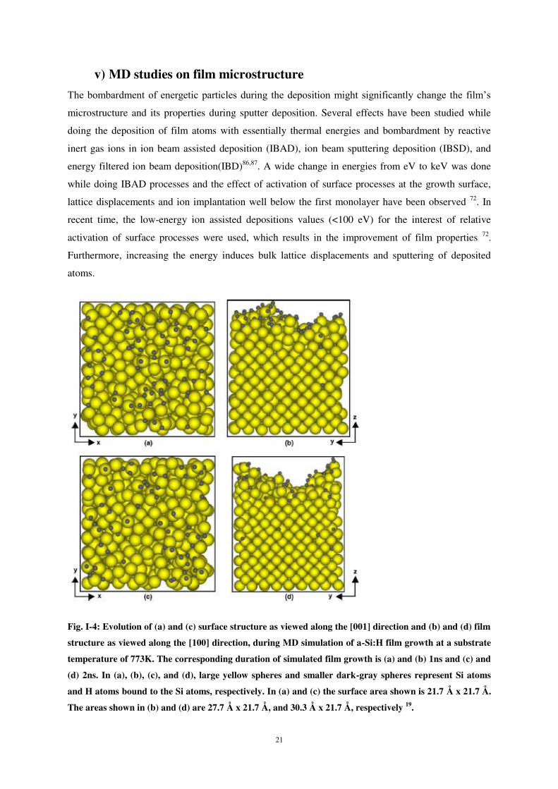
21
v) MD studies on film microstructure
The bombardment of energetic particles during the deposition might significantly change the film’s
microstructure and its properties during sputter deposition. Several effects have been studied while
doing the deposition of film atoms with essentially thermal energies and bombardment by reactive
inert gas ions in ion beam assisted deposition (IBAD), ion beam sputtering deposition (IBSD), and
energy filtered ion beam deposition(IBD)86,87. A wide change in energies from eV to keV was done
while doing IBAD processes and the effect of activation of surface processes at the growth surface,
lattice displacements and ion implantation well below the first monolayer have been observed 72. In
recent time, the low-energy ion assisted depositions values (<100 eV) for the interest of relative
activation of surface processes were used, which results in the improvement of film properties 72.
Furthermore, increasing the energy induces bulk lattice displacements and sputtering of deposited
atoms.
Fig. I-4: Evolution of (a) and (c) surface structure as viewed along the [001] direction and (b) and (d) film
structure as viewed along the [100] direction, during MD simulation of a-Si:H film growth at a substrate
temperature of 773K. The corresponding duration of simulated film growth is (a) and (b) 1ns and (c) and
(d) 2ns. In (a), (b), (c), and (d), large yellow spheres and smaller dark-gray spheres represent Si atoms
and H atoms bound to the Si atoms, respectively. In (a) and (c) the surface area shown is 21.7 Å x 21.7 Å.
The areas shown in (b) and (d) are 27.7 Å x 21.7 Å, and 30.3 Å x 21.7 Å, respectively 19.
22
M. S. Valipa et al. did a study on atomic scale analysis of fundamental processes that determine the
surface structure and smoothness during plasma deposition of hydrogenated amorphous silicon thin
films 19. They investigated the surface smoothness over different period of simulated growth time and
compare the results. Fig. I-4 gives the surface structures viewed along different directions and for
different growth times.
Several other cluster depositions are done by molecular dynamics simulations. J. C. Jimenez-Saez did
a molecular dynamics simulation study for Ni cluster deposition on a Cu (001) surface 88. The study
was mainly focusing on the understanding of the relation between the number of grown monolayers
and changes in the atomic positions near the interface. A low energy ion radiation study by molecular
dynamics simulation of Cu deposition on Mo (100) substrate has investigated by B.S. Bunnik et al. 89.
Due to the energetic impact of incident atoms, wetting phenomenon and different film structure were
observed
3) Plasma treatment
i) Introduction
Plasma can be defined as an ionized gas phase with a mixture of ions, electrons, photons, radicals and
neutral atoms. In this work, they are not investigated by themselves, or used during experiments.
However, the PhD work is a fundamental study on the interaction of few-eV energy atoms, i.e.
energies similar to those found in plasmas, with surfaces in order to understand the sticking and
deposition mechanisms with perspective to obtain results which could be used in later steps to
improve plasma processes.
In most of the cases in laboratory, plasmas are formed by applying an electric field which produces
accelerated electrons. Through collisions with atomic and molecular species, these electrons
dissociate, ionize and excite the gas phase species and form plasmas. Plasma occupies more than 99%
of the Universe, and we are living (on Earth) in the 1% where plasma does not predominate 90,91.
Various kinds of plasma exist. They can be classified according to their electron density and electron
energy (or temperature).
Due to the presence of various products issued from the plasma kinetics (dissociation, ionization,
recombination, excitation, etc.), plasmas are much more reactive than the natural gas mixture in which
they are sustained. So, such reactive plasmas are of great interest in plasma surface interaction and
therefore in surface processing.
Plasma based processes are efficient, environmental functional, non-polluting and economical tools
for surface treatment. The use of plasma-assisted surface treatments has been explored over many
decades in various application fields like textile industry, solar cell industry, semiconducting industry,
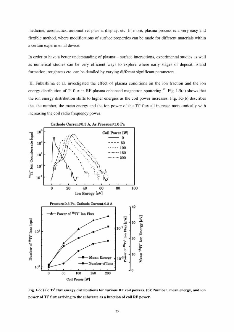
23
medicine, aeronautics, automotive, plasma display, etc. In more, plasma process is a very easy and
flexible method, where modifications of surface properties can be made for different materials within
a certain experimental device.
In order to have a better understanding of plasma – surface interactions, experimental studies as well
as numerical studies can be very efficient ways to explore where early stages of deposit, island
formation, roughness etc. can be detailed by varying different significant parameters.
K. Fukushima et al. investigated the effect of plasma conditions on the ion fraction and the ion
energy distribution of Ti flux in RF-plasma enhanced magnetron sputtering 92. Fig. I-5(a) shows that
the ion energy distribution shifts to higher energies as the coil power increases. Fig. I-5(b) describes
that the number, the mean energy and the ion power of the Ti+ flux all increase monotonically with
increasing the coil radio frequency power.
Fig. I-5: (a): Ti+ flux energy distributions for various RF coil powers. (b): Number, mean energy, and ion
power of Ti+ flux arriving to the substrate as a function of coil RF power.
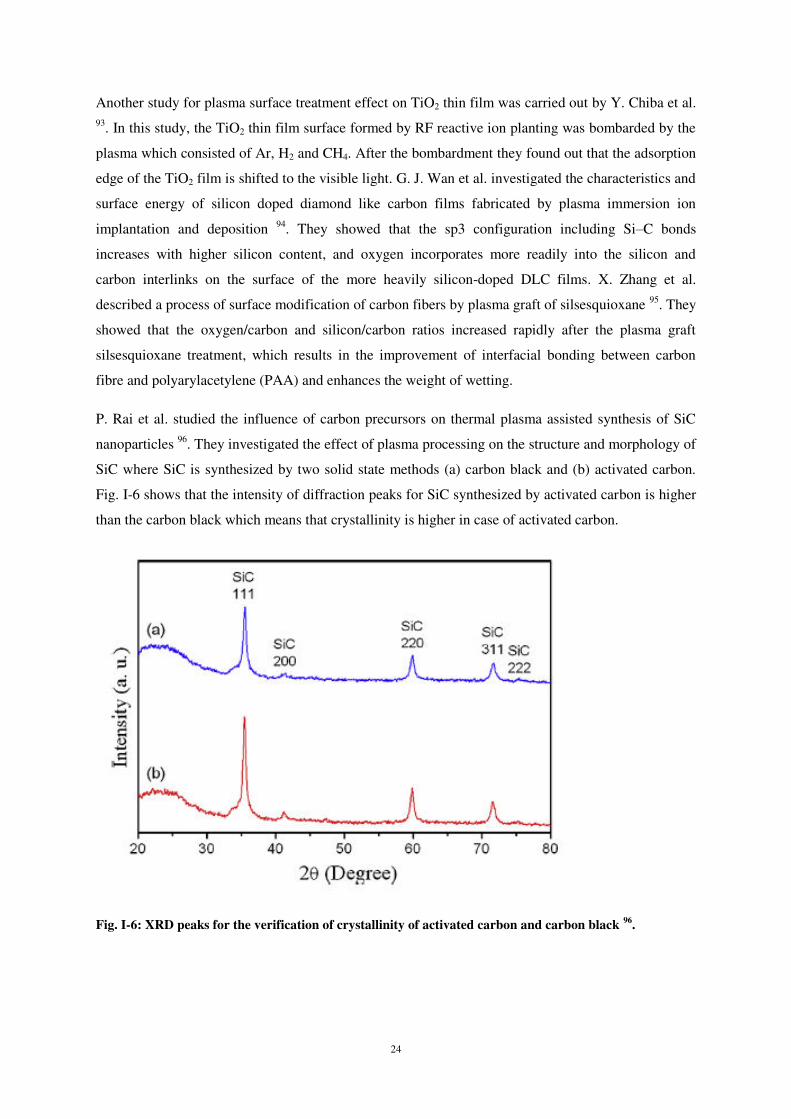
24
Another study for plasma surface treatment effect on TiO2 thin film was carried out by Y. Chiba et al. 93. In this study, the TiO2 thin film surface formed by RF reactive ion planting was bombarded by the
plasma which consisted of Ar, H2 and CH4. After the bombardment they found out that the adsorption
edge of the TiO2 film is shifted to the visible light. G. J. Wan et al. investigated the characteristics and
surface energy of silicon doped diamond like carbon films fabricated by plasma immersion ion
implantation and deposition 94. They showed that the sp3 configuration including Si–C bonds
increases with higher silicon content, and oxygen incorporates more readily into the silicon and
carbon interlinks on the surface of the more heavily silicon-doped DLC films. X. Zhang et al.
described a process of surface modification of carbon fibers by plasma graft of silsesquioxane 95. They
showed that the oxygen/carbon and silicon/carbon ratios increased rapidly after the plasma graft
silsesquioxane treatment, which results in the improvement of interfacial bonding between carbon
fibre and polyarylacetylene (PAA) and enhances the weight of wetting.
P. Rai et al. studied the influence of carbon precursors on thermal plasma assisted synthesis of SiC
nanoparticles 96. They investigated the effect of plasma processing on the structure and morphology of
SiC where SiC is synthesized by two solid state methods (a) carbon black and (b) activated carbon.
Fig. I-6 shows that the intensity of diffraction peaks for SiC synthesized by activated carbon is higher
than the carbon black which means that crystallinity is higher in case of activated carbon.
Fig. I-6: XRD peaks for the verification of crystallinity of activated carbon and carbon black 96.
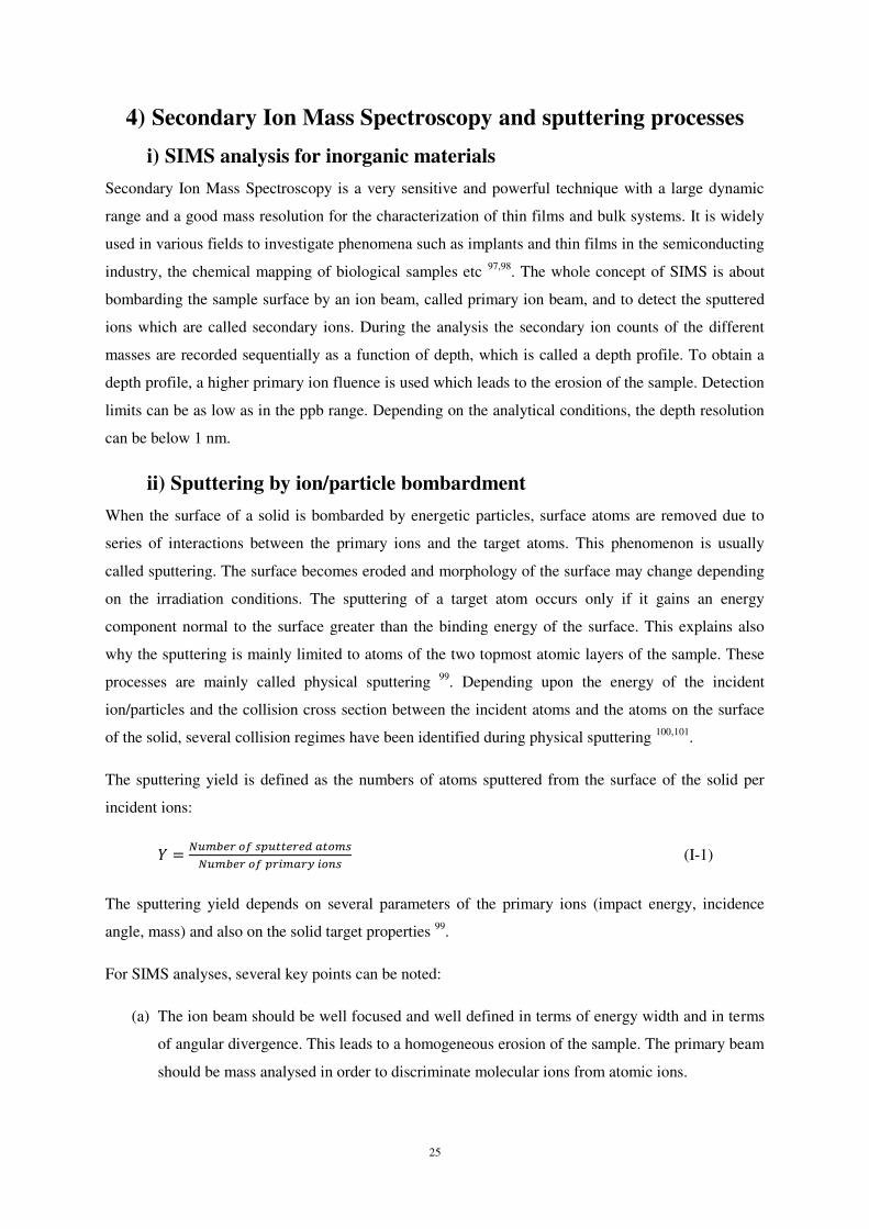
25
4) Secondary Ion Mass Spectroscopy and sputtering processes
i) SIMS analysis for inorganic materials
Secondary Ion Mass Spectroscopy is a very sensitive and powerful technique with a large dynamic
range and a good mass resolution for the characterization of thin films and bulk systems. It is widely
used in various fields to investigate phenomena such as implants and thin films in the semiconducting
industry, the chemical mapping of biological samples etc 97,98. The whole concept of SIMS is about
bombarding the sample surface by an ion beam, called primary ion beam, and to detect the sputtered
ions which are called secondary ions. During the analysis the secondary ion counts of the different
masses are recorded sequentially as a function of depth, which is called a depth profile. To obtain a
depth profile, a higher primary ion fluence is used which leads to the erosion of the sample. Detection
limits can be as low as in the ppb range. Depending on the analytical conditions, the depth resolution
can be below 1 nm.
ii) Sputtering by ion/particle bombardment
When the surface of a solid is bombarded by energetic particles, surface atoms are removed due to
series of interactions between the primary ions and the target atoms. This phenomenon is usually
called sputtering. The surface becomes eroded and morphology of the surface may change depending
on the irradiation conditions. The sputtering of a target atom occurs only if it gains an energy
component normal to the surface greater than the binding energy of the surface. This explains also
why the sputtering is mainly limited to atoms of the two topmost atomic layers of the sample. These
processes are mainly called physical sputtering 99. Depending upon the energy of the incident
ion/particles and the collision cross section between the incident atoms and the atoms on the surface
of the solid, several collision regimes have been identified during physical sputtering 100,101.
The sputtering yield is defined as the numbers of atoms sputtered from the surface of the solid per
incident ions:
(I-1)
The sputtering yield depends on several parameters of the primary ions (impact energy, incidence
angle, mass) and also on the solid target properties 99.
For SIMS analyses, several key points can be noted:
(a) The ion beam should be well focused and well defined in terms of energy width and in terms
of angular divergence. This leads to a homogeneous erosion of the sample. The primary beam
should be mass analysed in order to discriminate molecular ions from atomic ions.
26
(b) During the initial stage of bombardment, the amount of primary ions being implanted into the
target material is higher than the one being sputtered, which will modify the secondary ion
yield depending on the reactivity of the primary ion species. Indeed, ionisation processes in
SIMS depend on the local sample composition. Therefore, any change in the surface atom
environment may result in a change in the secondary ion yields and also the sputtering yield.
Similarly, in the case of thin film analysis, if the investigated layer is too thin, the underlying
substrate may influence the secondary ion yield and sputtering yield 102.
Besides experimental observations, several computer simulations by binary collision approximations
have been done to measure the sputtering yield. B. Guzmán de la Mata et al. investigated sputter yield
variations of diamond films under bombardment with low energy ions. Fig. I-7 describes the sputter
yield variations as a function of angle for cesium beam at 500 eV 103. The behaviour has almost same
trend for three different materials. The sputter yield increases for lower range of angles (<50°) and
becomes maximum between 40° and 70°. This behaviour is true for any analytical conditions in
dynamic SIMS, i.e. monatomic primary ions and energy in the keV range. They explained that the
decrease is due to enhanced scattering of the caesium at glancing angles and may also be due to onset
of roughness. In their work, they observed also the variation of the sputter yield by using 500 eV O2
beam. In this case they found only increasing nature of sputter yield with angle even at 70°. Data for
larger angles is not available, but the sputter yield is expected to decrease at some point 103.
Fig. I-7 : Sputter yield dependence on angle for several materials bombarded with a 500eV caesium beam
taken from reference 103.
Fig. I-8 describes the dependence of sputter yield on impact energy. The experiment was done at 50°
incidence angle with respect to the surface normal for a caesium beam by B.G. Mata et al. In the
energy range for SIMS, the sputter yield increases with energy for all the materials 103.
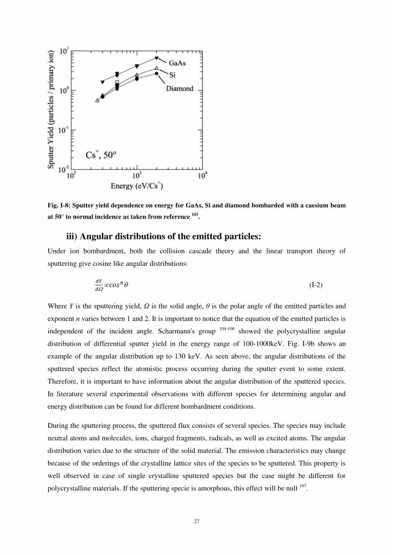
27
Fig. I-8: Sputter yield dependence on energy for GaAs, Si and diamond bombarded with a caesium beam
at 50° to normal incidence as taken from reference 103.
iii) Angular distributions of the emitted particles:
Under ion bombardment, both the collision cascade theory and the linear transport theory of
sputtering give cosine like angular distributions:
(I-2)
Where Y is the sputtering yield, Ω is the solid angle, θ is the polar angle of the emitted particles and
exponent n varies between 1 and 2. It is important to notice that the equation of the emitted particles is
independent of the incident angle. Scharmann's group 104-106 showed the polycrystalline angular
distribution of differential sputter yield in the energy range of 100-1000keV. Fig. I-9b shows an
example of the angular distribution up to 130 keV. As seen above, the angular distributions of the
sputtered species reflect the atomistic process occurring during the sputter event to some extent.
Therefore, it is important to have information about the angular distribution of the sputtered species.
In literature several experimental observations with different species for determining angular and
energy distribution can be found for different bombardment conditions.
During the sputtering process, the sputtered flux consists of several species. The species may include
neutral atoms and molecules, ions, charged fragments, radicals, as well as excited atoms. The angular
distribution varies due to the structure of the solid material. The emission characteristics may change
because of the orderings of the crystalline lattice sites of the species to be sputtered. This property is
well observed in case of single crystalline sputtered species but the case might be different for
polycrystalline materials. If the sputtering specie is amorphous, this effect will be null 107.
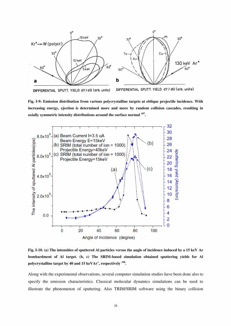
28
Fig. I-9: Emission distribution from various polycrystalline targets at oblique projectile incidence. With
increasing energy, ejection is determined more and more by random collision cascades, resulting in
axially symmetric intensity distributions around the surface normal 107.
Fig. I-10. (a) The intensities of sputtered Al particles versus the angle of incidence induced by a 15 keV Ar
bombardment of Al target. (b, c) The SRIM-based simulation obtained sputtering yields for Al
polycrystalline target by 40 and 15 keVAr+, respectively 108.
Along with the experimental observations, several computer simulation studies have been done also to
specify the emission characteristics. Classical molecular dynamics simulations can be used to
illustrate the phenomenon of sputtering. Also TRIM/SRIM software using the binary collision
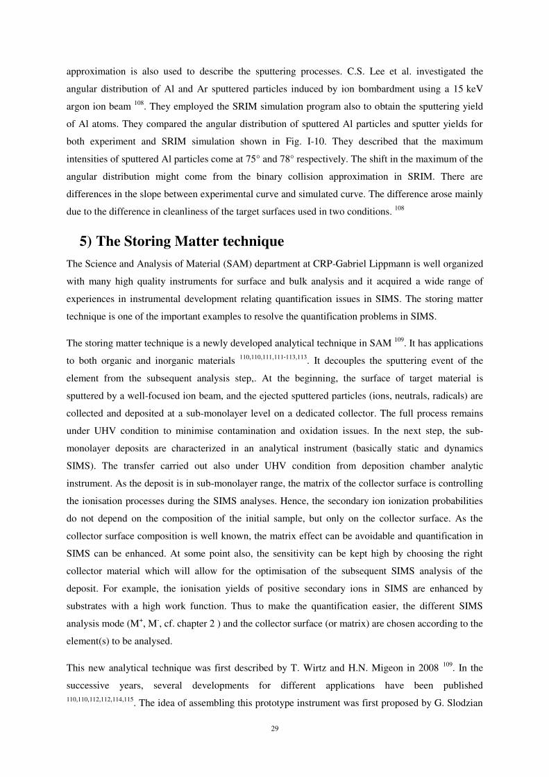
29
approximation is also used to describe the sputtering processes. C.S. Lee et al. investigated the
angular distribution of Al and Ar sputtered particles induced by ion bombardment using a 15 keV
argon ion beam 108. They employed the SRIM simulation program also to obtain the sputtering yield
of Al atoms. They compared the angular distribution of sputtered Al particles and sputter yields for
both experiment and SRIM simulation shown in Fig. I-10. They described that the maximum
intensities of sputtered Al particles come at 75° and 78° respectively. The shift in the maximum of the
angular distribution might come from the binary collision approximation in SRIM. There are
differences in the slope between experimental curve and simulated curve. The difference arose mainly
due to the difference in cleanliness of the target surfaces used in two conditions. 108
5) The Storing Matter technique The Science and Analysis of Material (SAM) department at CRP-Gabriel Lippmann is well organized
with many high quality instruments for surface and bulk analysis and it acquired a wide range of
experiences in instrumental development relating quantification issues in SIMS. The storing matter
technique is one of the important examples to resolve the quantification problems in SIMS.
The storing matter technique is a newly developed analytical technique in SAM 109. It has applications
to both organic and inorganic materials 110,110,111,111-113,113. It decouples the sputtering event of the
element from the subsequent analysis step,. At the beginning, the surface of target material is
sputtered by a well-focused ion beam, and the ejected sputtered particles (ions, neutrals, radicals) are
collected and deposited at a sub-monolayer level on a dedicated collector. The full process remains
under UHV condition to minimise contamination and oxidation issues. In the next step, the sub-
monolayer deposits are characterized in an analytical instrument (basically static and dynamics
SIMS). The transfer carried out also under UHV condition from deposition chamber analytic
instrument. As the deposit is in sub-monolayer range, the matrix of the collector surface is controlling
the ionisation processes during the SIMS analyses. Hence, the secondary ion ionization probabilities
do not depend on the composition of the initial sample, but only on the collector surface. As the
collector surface composition is well known, the matrix effect can be avoidable and quantification in
SIMS can be enhanced. At some point also, the sensitivity can be kept high by choosing the right
collector material which will allow for the optimisation of the subsequent SIMS analysis of the
deposit. For example, the ionisation yields of positive secondary ions in SIMS are enhanced by
substrates with a high work function. Thus to make the quantification easier, the different SIMS
analysis mode (M+, M-, cf. chapter 2 ) and the collector surface (or matrix) are chosen according to the
element(s) to be analysed.
This new analytical technique was first described by T. Wirtz and H.N. Migeon in 2008 109. In the
successive years, several developments for different applications have been published 110,110,112,112,114,115. The idea of assembling this prototype instrument was first proposed by G. Slodzian
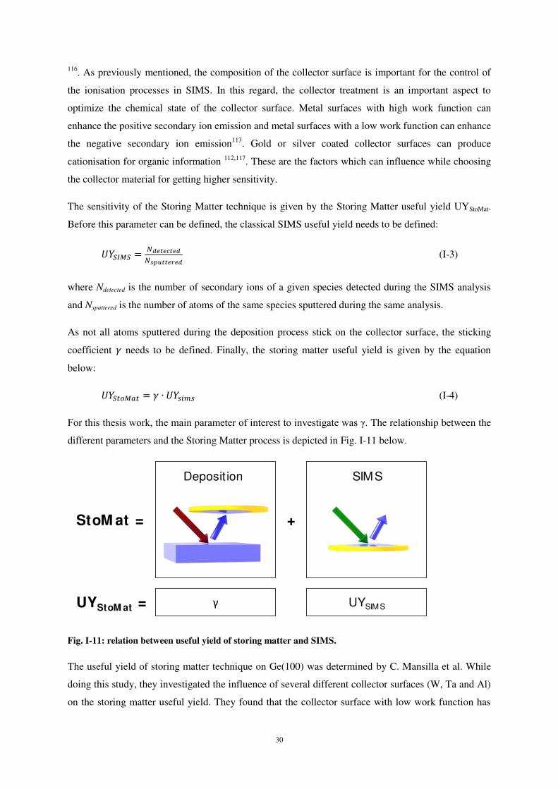
30
116. As previously mentioned, the composition of the collector surface is important for the control of
the ionisation processes in SIMS. In this regard, the collector treatment is an important aspect to
optimize the chemical state of the collector surface. Metal surfaces with high work function can
enhance the positive secondary ion emission and metal surfaces with a low work function can enhance
the negative secondary ion emission113. Gold or silver coated collector surfaces can produce
cationisation for organic information 112,117. These are the factors which can influence while choosing
the collector material for getting higher sensitivity.
The sensitivity of the Storing Matter technique is given by the Storing Matter useful yield UYStoMat.
Before this parameter can be defined, the classical SIMS useful yield needs to be defined:
(I-3)
where Ndetected is the number of secondary ions of a given species detected during the SIMS analysis
and Nsputtered is the number of atoms of the same species sputtered during the same analysis.
As not all atoms sputtered during the deposition process stick on the collector surface, the sticking
coefficient needs to be defined. Finally, the storing matter useful yield is given by the equation
below: (I-4)
For this thesis work, the main parameter of interest to investigate was γ. The relationship between the
different parameters and the Storing Matter process is depicted in Fig. I-11 below.
Fig. I-11: relation between useful yield of storing matter and SIMS.
The useful yield of storing matter technique on Ge(100) was determined by C. Mansilla et al. While
doing this study, they investigated the influence of several different collector surfaces (W, Ta and Al)
on the storing matter useful yield. They found that the collector surface with low work function has
StoM at = +
Deposit ion SIMS
γ • UYSIMSUYStoM at =
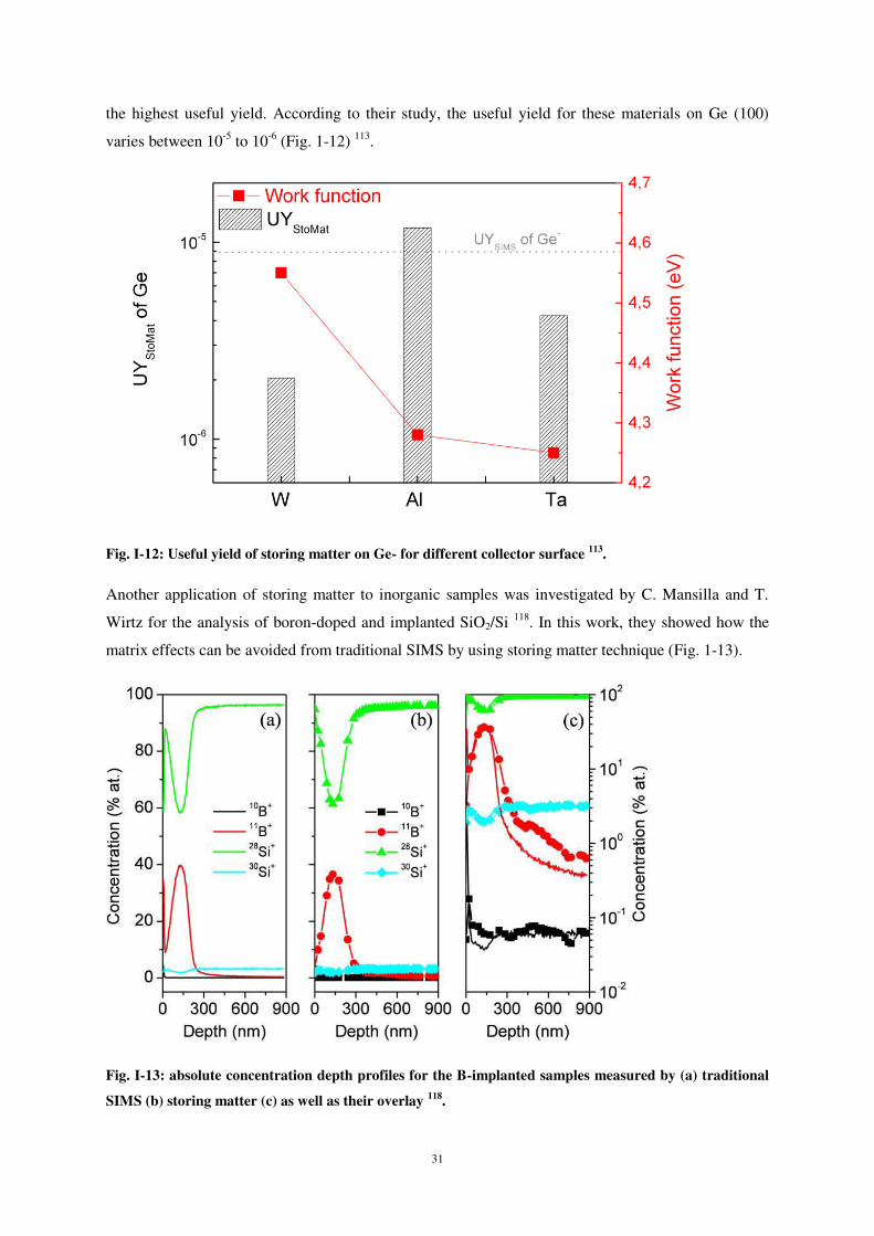
31
the highest useful yield. According to their study, the useful yield for these materials on Ge (100)
varies between 10-5 to 10-6 (Fig. 1-12) 113.
Fig. I-12: Useful yield of storing matter on Ge- for different collector surface 113.
Another application of storing matter to inorganic samples was investigated by C. Mansilla and T.
Wirtz for the analysis of boron-doped and implanted SiO2/Si 118. In this work, they showed how the
matrix effects can be avoided from traditional SIMS by using storing matter technique (Fig. 1-13).
Fig. I-13: absolute concentration depth profiles for the B-implanted samples measured by (a) traditional
SIMS (b) storing matter (c) as well as their overlay 118.

32
However, several other inorganic materials have been tested by other users for storing matter but
experiments for the calculation of sticking coefficient for titanium and tungsten have not been done
before. Calculation of useful yield of tungsten (W) as a collector surface on Ge (100) was performed
by Mansilla et al. 113, and Philipp et al. 110 studied the useful yield of titanium (Ti) in storing matter
instrument but sticking efficiency of Ti and W on Si (100) was never investigated before in storing
matter instrument. Another material of interest to be tested was carbon on silicon on storing matter
instrument but we did only simulation calculations for carbon as it is very prone to contaminations. In
the following chapter, we will discuss details of the techniques and results related to sticking and
deposition of carbon, titanium and tungsten on silicon surfaces.
33
Techniques and Conditions
“This PhD work involves both experimental and
simulation analysis. The details of techniques and
conditions implemented for different inorganic
particle interactions are discussed in this chapter.”

34
35
Chapitre 2.
Techniques and conditions
1) Introduction As the SubML project deals with a multidisciplinary approach, several techniques have been
employed to accomplish the project targets. The main three techniques used in the SubML project are
molecular dynamics simulations, sputter deposition in the storing matter instrument and SIMS
analysis technique. We will describe first molecular dynamics simulation details followed by storing
matter and SIMS description along with the conditions used during the project.
2) Simulation techniques For the numerical simulation work of this project, we choose MD method as it is the most promising
simulation tool to provide a totally predictable description of the system of interest over short span of
time and it provides detailed explanations of the atomistic characteristics during the deposition
process. For the simulations we used the MD code (FLX) developed by J. Kieffer et al.61,61 which was
developed for the modeling of materials with mixed ionic-covalent bonding character. As such, FLX
offers a choice of interaction models, including Lennard-Jones, Coulomb, Born-Mayer-Huggins,
three-body, and Kieffer’s model of charge-transfer. FLX uses a fifth-order Gear predictor-correct
scheme for the integration of the equations of motion.
FLX gathers input from one or maximally two files, the control file and a configuration file. The
control file contains information about the chemical constitution of the system to be simulated and
run-time options pertaining to the collection of statistical information. The configuration file contains
the initial coordinates, velocities, instantaneous forces, 3rd and 4th derivatives of all dynamical
variables. This file is only necessary if a system’s evolution is observed over subsequent runs, i.e., the
initial configuration of one run is typically the ending configuration of a preceding run. For new runs,
the positions within a unit cell are defined within the control file. The configuration file also contains
information about the run history of a configuration, allowing one to trace the evolution of a structure
and the various conditions that it has been subjected to.
We will describe now the pressure and temperature algorithms used in FLX. Constant pressure
general Parinello-Rahman (PR) (9 degrees of freedom) algorithm has been used in the calculations.
The general PR algorithm includes 9 parameters to define the simulation box. They are 3 length and 3
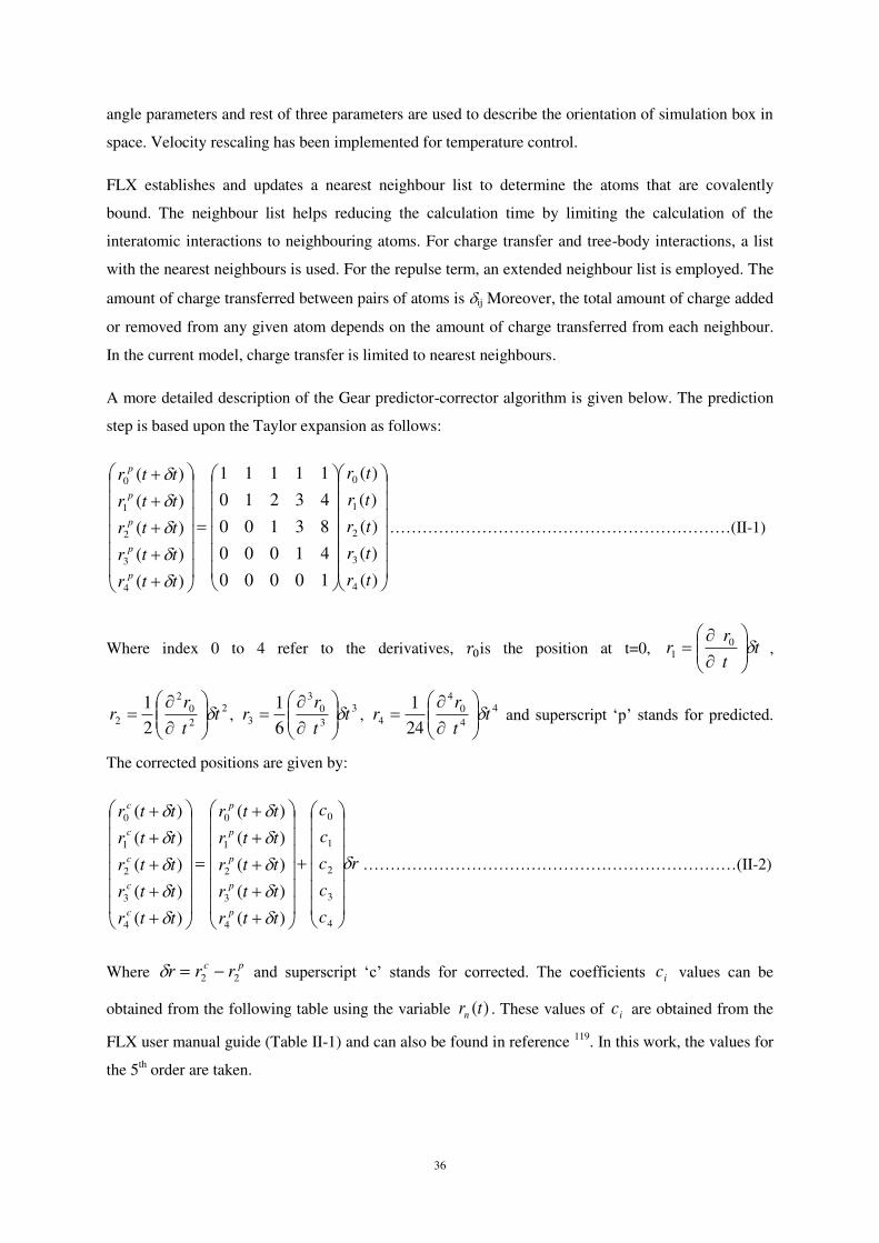
36
angle parameters and rest of three parameters are used to describe the orientation of simulation box in
space. Velocity rescaling has been implemented for temperature control.
FLX establishes and updates a nearest neighbour list to determine the atoms that are covalently
bound. The neighbour list helps reducing the calculation time by limiting the calculation of the
interatomic interactions to neighbouring atoms. For charge transfer and tree-body interactions, a list
with the nearest neighbours is used. For the repulse term, an extended neighbour list is employed. The
amount of charge transferred between pairs of atoms is ij Moreover, the total amount of charge added
or removed from any given atom depends on the amount of charge transferred from each neighbour.
In the current model, charge transfer is limited to nearest neighbours.
A more detailed description of the Gear predictor-corrector algorithm is given below. The prediction
step is based upon the Taylor expansion as follows:
)(
)(
)(
)(
)(
10000
41000
83100
43210
11111
)(
)(
)(
)(
)(
4
3
2
1
0
4
3
2
1
0
tr
tr
tr
tr
tr
ttr
ttr
ttr
ttr
ttr
p
p
p
p
p
………………………………………………………(II-1)
Where index 0 to 4 refer to the derivatives, is the position at t=0, tt
rr
01 ,
220
2
2 21
tt
rr
, 330
3
3 61
tt
rr
, 440
4
4 241
tt
rr
and superscript ‘p’ stands for predicted.
The corrected positions are given by:
r
c
c
c
c
c
ttr
ttr
ttr
ttr
ttr
ttr
ttr
ttr
ttr
ttr
p
p
p
p
p
c
c
c
c
c
4
3
2
1
0
4
3
2
1
0
4
3
2
1
0
)(
)(
)(
)(
)(
)(
)(
)(
)(
)(
……………………………………………………………(II-2)
Where pcrrr 22 and superscript ‘c’ stands for corrected. The coefficients ic values can be
obtained from the following table using the variable )(trn . These values of ic are obtained from the
FLX user manual guide (Table II-1) and can also be found in reference 119. In this work, the values for
the 5th order are taken.
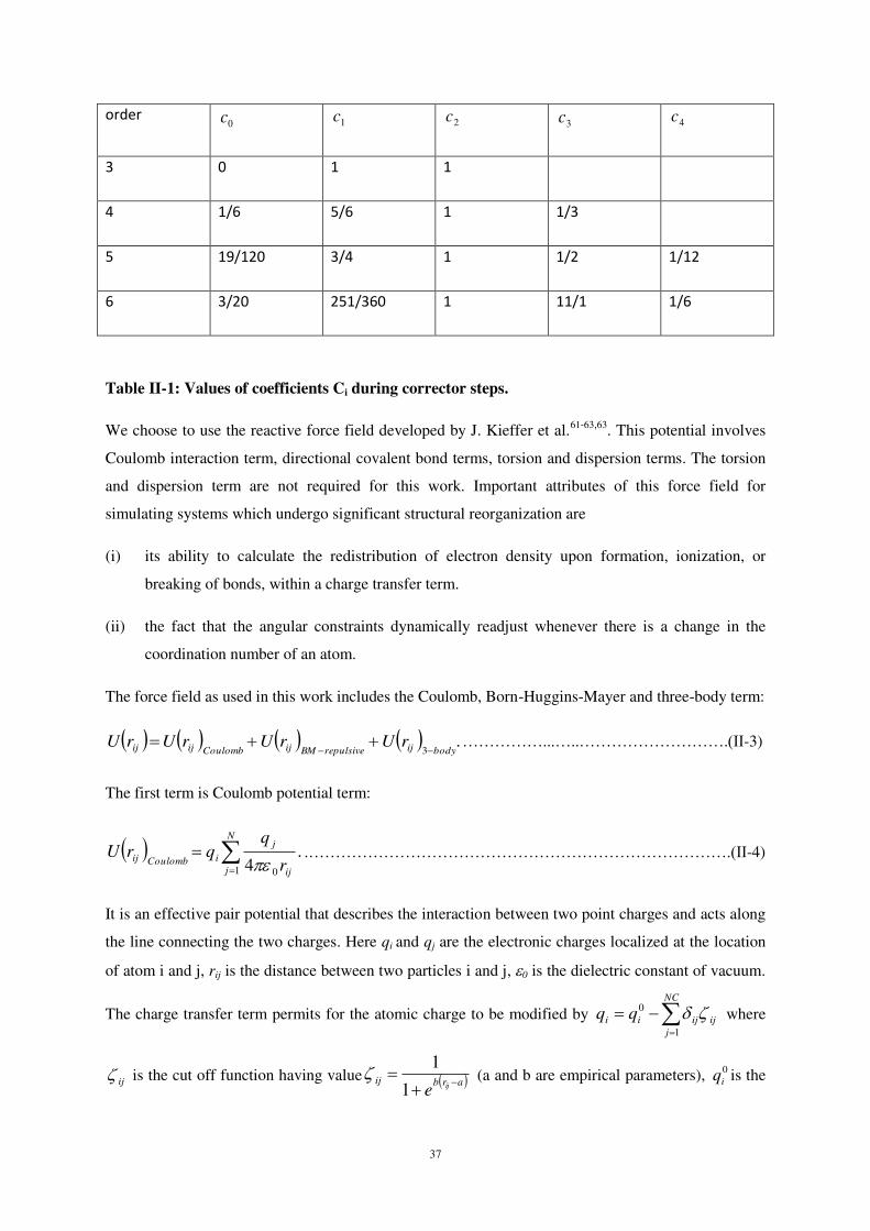
37
order 0c 1c 2c 3c 4c
3 0 1 1
4 1/6 5/6 1 1/3
5 19/120 3/4 1 1/2 1/12
6 3/20 251/360 1 11/1 1/6
Table II-1: Values of coefficients Ci during corrector steps.
We choose to use the reactive force field developed by J. Kieffer et al.61-63,63. This potential involves
Coulomb interaction term, directional covalent bond terms, torsion and dispersion terms. The torsion
and dispersion term are not required for this work. Important attributes of this force field for
simulating systems which undergo significant structural reorganization are
(i) its ability to calculate the redistribution of electron density upon formation, ionization, or
breaking of bonds, within a charge transfer term.
(ii) the fact that the angular constraints dynamically readjust whenever there is a change in the
coordination number of an atom.
The force field as used in this work includes the Coulomb, Born-Huggins-Mayer and three-body term:
.3 bodyijrepulsiveBMijCoulombijij rUrUrUrU
……………...…..……………………….(II-3)
The first term is Coulomb potential term:
N
j ij
j
iCoulombijr
qqrU
1 0
.4
.…………………………………………………………………….(II-4)
It is an effective pair potential that describes the interaction between two point charges and acts along
the line connecting the two charges. Here qi and qj are the electronic charges localized at the location
of atom i and j, rij is the distance between two particles i and j, 0 is the dielectric constant of vacuum.
The charge transfer term permits for the atomic charge to be modified by
NC
j
ijijii qq1
0 where
ij is the cut off function having value arbijije
1
1 (a and b are empirical parameters), 0iq is the
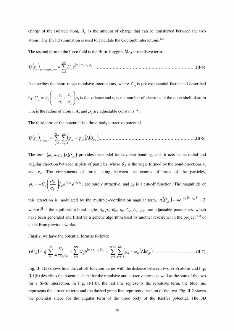
38
charge of the isolated atom, ij is the amount of charge that can be transferred between the two
atoms. The Ewald summation is used to calculate the Coulomb interactions.120
The second term in the force field is the Born-Huggins-Mayer repulsive term.
NC
i
r
ijrepulsiveBMij
ijijjieCrU1
…………………………………………………………….(II-5)
It describes the short range repulsive interactions, where ijC is pre-exponential factor and described
by
j
j
i
iijij
n
z
n
zAC 1 ,zi is the valence and ni is the number of electrons in the outer shell of atom
i, σi is the radius of atom i, Aij and ij are adjustable constants 121.
The third term of the potential is a three-body attractive potential.
1
1 13
NC
j
NC
jk
ijkikijbodyijrU ………………………………………………………….(II-6)
The term ijkikij provides the model for covalent bonding, and it acts in the radial and
angular direction between triplets of particles, where ijk is the angle formed by the bond directions rij
and rik. The components of force acting between the centres of mass of the particles,
ijijijij r
ij
ij
ij
ijij eeC
, are purely attractive, and ij is a cut-off function. The magnitude of
this attraction is modulated by the multiple-coordination angular term, 344
ijkijkeijk
where ̅ is the equilibrium bond angle. Aij, ij, ijk, ij, CZ, AZ, ijk, are adjustable parameters, which
have been generated and fitted by a genetic algorithm used by another researcher in the project 121 or
taken from previous works.
Finally, we have the potential form as follows:
1
1 111 04
NC
j
NC
jk
ijkikij
NC
i
r
ij
N
j ij
j
iijijijjieC
r
qqrU
……………………..…..(II-7)
Fig. II- 1(a) shows how the cut-off function varies with the distance between two Si-Si atoms and Fig.
II-1(b) describes the potential shape for the repulsive and attractive term, as well as the sum of the two
for a Si-Si interaction. In Fig. II-1(b), the red line represents the repulsive term, the blue line
represents the attractive term and the dashed green line represents the sum of the two. Fig. II-2 shows
the potential shape for the angular term of the three body of the Kieffer potential. The 3D
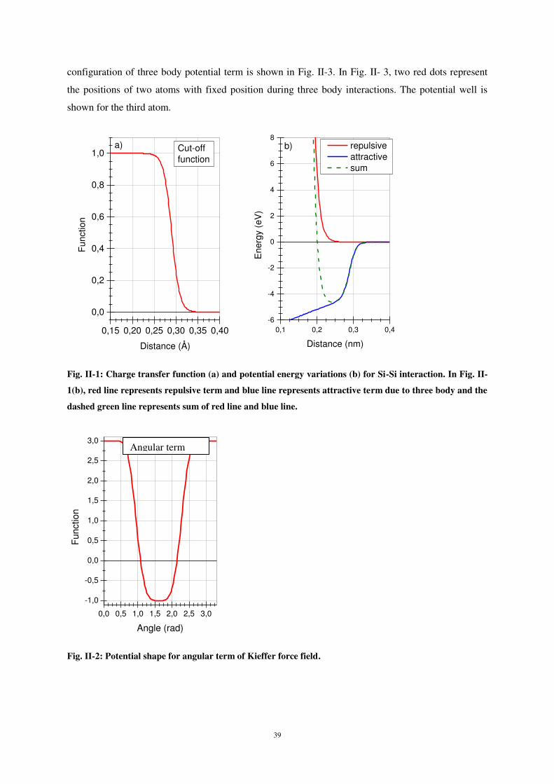
39
configuration of three body potential term is shown in Fig. II-3. In Fig. II- 3, two red dots represent
the positions of two atoms with fixed position during three body interactions. The potential well is
shown for the third atom.
Fig. II-1: Charge transfer function (a) and potential energy variations (b) for Si-Si interaction. In Fig. II-
1(b), red line represents repulsive term and blue line represents attractive term due to three body and the
dashed green line represents sum of red line and blue line.
Fig. II-2: Potential shape for angular term of Kieffer force field.
0,15 0,20 0,25 0,30 0,35 0,40
0,0
0,2
0,4
0,6
0,8
1,0
Fun
ctio
n
Distance (Å)
a) Cut-offfunction
0,1 0,2 0,3 0,4-6
-4
-2
0
2
4
6
8
Ene
rgy
(eV
)
Distance (nm)
repulsive attractive sum
b)
0,0 0,5 1,0 1,5 2,0 2,5 3,0
-1,0
-0,5
0,0
0,5
1,0
1,5
2,0
2,5
3,0
Fun
ctio
n
Angle (rad)
Angular term
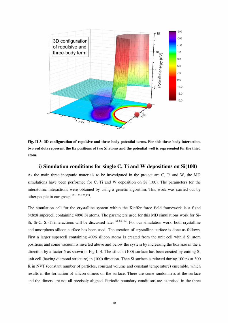
40
Fig. II-3: 3D configuration of repulsive and three body potential terms. For this three body interaction,
two red dots represent the fix positions of two Si atoms and the potential well is represented for the third
atom.
i) Simulation conditions for single C, Ti and W depositions on Si(100)
As the main three inorganic materials to be investigated in the project are C, Ti and W, the MD
simulations have been performed for C, Ti and W deposition on Si (100). The parameters for the
interatomic interactions were obtained by using a genetic algorithm. This work was carried out by
other people in our group 121-123,123,124.
The simulation cell for the crystalline system within the Kieffer force field framework is a fixed
8x8x8 supercell containing 4096 Si atoms. The parameters used for this MD simulations work for Si-
Si, Si-C, Si-Ti interactions will be discussed later 61-63,122. For our simulation work, both crystalline
and amorphous silicon surface has been used. The creation of crystalline surface is done as follows.
First a larger supercell containing 4096 silicon atoms is created from the unit cell with 8 Si atom
positions and some vacuum is inserted above and below the system by increasing the box size in the z
direction by a factor 5 as shown in Fig II-4. The silicon (100) surface has been created by cutting Si
unit cell (having diamond structure) in (100) direction. Then Si surface is relaxed during 100 ps at 300
K in NVT (constant number of particles, constant volume and constant temperature) ensemble, which
results in the formation of silicon dimers on the surface. There are some randomness at the surface
and the dimers are not all precisely aligned. Periodic boundary conditions are exercised in the three
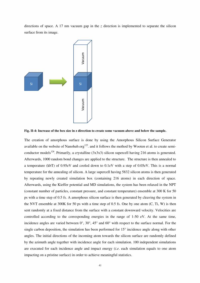
41
directions of space. A 17 nm vacuum gap in the z direction is implemented to separate the silicon
surface from its image.
Fig. II-4: Increase of the box size in z direction to create some vacuum above and below the sample.
The creation of amorphous surface is done by using the Amorphous Silicon Surface Generator
available on the website of Nanohub.org125. and it follows the method by Wooten et al. to create semi-
conductor models126. Primarily, a crystalline (3x3x3) silicon supercell having 216 atoms is generated.
Afterwards, 1000 random bond changes are applied to the structure. The structure is then annealed to
a temperature (kbT) of 0.95eV and cooled down to 0.1eV with a step of 0.05eV. This is a normal
temperature for the annealing of silicon. A large supercell having 5832 silicon atoms is then generated
by repeating newly created simulation box (containing 216 atoms) in each direction of space.
Afterwards, using the Kieffer potential and MD simulations, the system has been relaxed in the NPT
(constant number of particles, constant pressure, and constant temperature) ensemble at 300 K for 50
ps with a time step of 0.5 fs. A amorphous silicon surface is then generated by cleaving the system in
the NVT ensemble at 300K for 50 ps with a time step of 0.5 fs. One by one atom (C, Ti, W) is then
sent randomly at a fixed distance from the surface with a constant downward velocity. Velocities are
controlled according to the corresponding energies in the range of 1-50 eV. At the same time,
incidence angles are varied between 0°, 30°, 45° and 60° with respect to the surface normal. For the
single carbon deposition, the simulation has been performed for 15° incidence angle along with other
angles. The initial directions of the incoming atom towards the silicon surface are randomly defined
by the azimuth angle together with incidence angle for each simulation. 100 independent simulations
are executed for each incidence angle and impact energy (i.e. each simulation equals to one atom
impacting on a pristine surface) in order to achieve meaningful statistics.
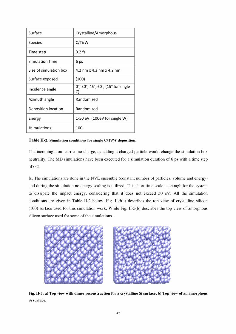
42
Surface Crystalline/Amorphous
Species C/Ti/W
Time step 0.2 fs
Simulation Time 6 ps
Size of simulation box 4.2 nm x 4.2 nm x 4.2 nm
Surface exposed (100)
Incidence angle 0°, 30°, 45°, 60°, (15° for single
C)
Azimuth angle Randomized
Deposition location Randomized
Energy 1-50 eV, (100eV for single W)
#simulations 100
Table II-2: Simulation conditions for single C/Ti/W deposition.
The incoming atom carries no charge, as adding a charged particle would change the simulation box
neutrality. The MD simulations have been executed for a simulation duration of 6 ps with a time step
of 0.2
fs. The simulations are done in the NVE ensemble (constant number of particles, volume and energy)
and during the simulation no energy scaling is utilized. This short time scale is enough for the system
to dissipate the impact energy, considering that it does not exceed 50 eV. All the simulation
conditions are given in Table II-2 below. Fig. II-5(a) describes the top view of crystalline silicon
(100) surface used for this simulation work, While Fig. II-5(b) describes the top view of amorphous
silicon surface used for some of the simulations.
Fig. II-5: a) Top view with dimer reconstruction for a crystalline Si surface, b) Top view of an amorphous
Si surface.
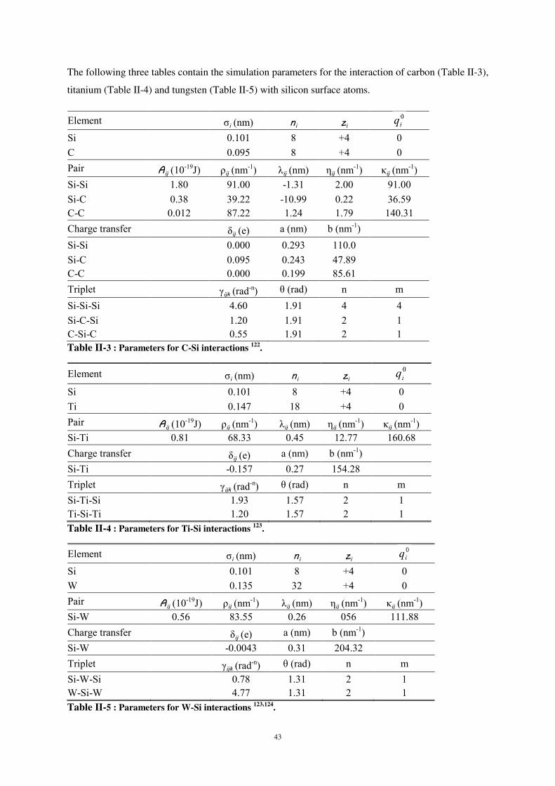
43
The following three tables contain the simulation parameters for the interaction of carbon (Table II-3),
titanium (Table II-4) and tungsten (Table II-5) with silicon surface atoms.
Element σi (nm) ni zi Si 0.101 8 +4 0
C 0.095 8 +4 0
Pair Aij (10-19
J) ρij (nm-1
) ij (nm) ij (nm-1
) ij (nm-1
)
Si-Si 1.80 91.00 -1.31 2.00 91.00
Si-C 0.38 39.22 -10.99 0.22 36.59
C-C 0.012 87.22 1.24 1.79 140.31
Charge transfer δij (e) a (nm) b (nm-1
)
Si-Si 0.000 0.293 110.0
Si-C 0.095 0.243 47.89
C-C 0.000 0.199 85.61
Triplet γijk (rad-n
) (rad) n m
Si-Si-Si 4.60 1.91 4 4
Si-C-Si 1.20 1.91 2 1
C-Si-C 0.55 1.91 2 1
Table II-3 : Parameters for C-Si interactions 122.
Element σi (nm) ni zi Si 0.101 8 +4 0
Ti 0.147 18 +4 0
Pair Aij (10-19
J) ρij (nm-1
) ij (nm) ij (nm-1
) ij (nm-1
)
Si-Ti 0.81 68.33 0.45 12.77 160.68
Charge transfer δij (e) a (nm) b (nm-1
)
Si-Ti -0.157 0.27 154.28
Triplet γijk (rad-n
) (rad) n m
Si-Ti-Si 1.93 1.57 2 1
Ti-Si-Ti 1.20 1.57 2 1
Table II-4 : Parameters for Ti-Si interactions 123.
Element σi (nm) ni zi Si 0.101 8 +4 0
W 0.135 32 +4 0
Pair Aij (10-19
J) ρij (nm-1
) ij (nm) ij (nm-1
) ij (nm-1
)
Si-W 0.56 83.55 0.26 056 111.88
Charge transfer δij (e) a (nm) b (nm-1
)
Si-W -0.0043 0.31 204.32
Triplet γijk (rad-n
) (rad) n m
Si-W-Si 0.78 1.31 2 1
W-Si-W 4.77 1.31 2 1
Table II-5 : Parameters for W-Si interactions 123,124.
44
ii) Simulation conditions for multiple impacts of C on Si (100)
Along with this, there was another simulation frame designed to execute continuous atom deposition
in order to have better comparison with experimental observations. Here MD simulations are also
performed using the reactive force field described by J. Kieffer and his co-workers 61-63. The
parameters for Si-Si and Si-C interactions are presented in 122 and in table II-3. For the continuous
carbon deposition on the Si(100) surface, similar conditions have been used than for single carbon
deposition 122 for the deposition of multiple carbon atoms on a Si(100) surface. The deposition of each
carbon in a continuous fashion has to be divided into two steps: a deposition step and a cooling step.
The cooling step, consisting of a ramping of the temperature back to 300 K during 4 ps, is used after
the deposition of each atom. The azimuth angle for these simulations has been fixed at 0° and 45°.
For the results’ analyses, the implantation depth is defined as the average vertical distance between
the carbon atom at the end of each MD simulation and the surface plane. For the Si(100) surface, the
surface plane is simply defined by the z coordinate of the topmost silicon atom. For all conditions, the
reflected atoms are ignored in the calculations of depth and angular distributions. In order to get some
information on the structure formed, the system has been divided in the z direction into different
slabs. Each slab has a thickness of 5.0 Å. In the graphs they are identified by the centre position of the
slab, i.e. 2.5 Å for the first slab, 7.5 Å for the second, etc. We choose 5 Å thick slab arbitrarily and it
is quite close to the lattice dimensions for the Si diamond structure, which is 5.43 Å.
The simulation conditions are same as single carbon deposition except azimuth angle which are set at
0° and 45°.
3) Experimental techniques In order to investigate the sticking, deposition and reorganization of the inorganic materials Ti and W
on silicon Si(100) surfaces experimentally, we employed storing matter deposition technique along
with dynamic SIMS analysis technique. We will first discuss the sputter deposition process in storing
matter technique and used conditions for the deposits followed by the description of the SIMS
instrument employed and the conditions used.
i) Storing matter technique: principle and instrumental description
Here we will focus on the description of several parts of the storing matter instrument.
As our main point of interest is to investigate deposition and sticking behaviour of inorganic materials
on silicon substrate in the sub-monolayer range, the storing matter instrument is particularly suitable
since it is specifically designed to achieve sub-monolayer deposits. Controlling primary current and
the time of the deposit, several sub-monolayer deposits are achieved. Fig. II-6 shows the schematic
diagram of prototype storing matter instrument.
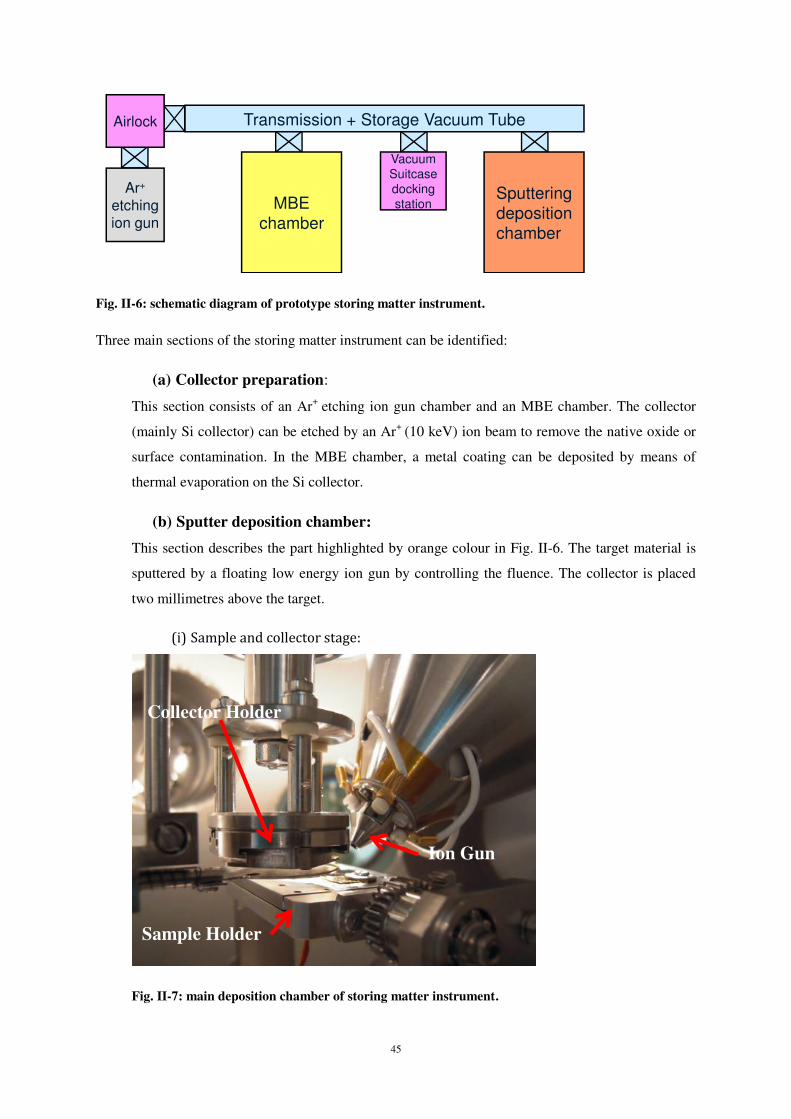
45
Fig. II-6: schematic diagram of prototype storing matter instrument.
Three main sections of the storing matter instrument can be identified:
(a) Collector preparation:
This section consists of an Ar+ etching ion gun chamber and an MBE chamber. The collector
(mainly Si collector) can be etched by an Ar+ (10 keV) ion beam to remove the native oxide or
surface contamination. In the MBE chamber, a metal coating can be deposited by means of
thermal evaporation on the Si collector.
(b) Sputter deposition chamber:
This section describes the part highlighted by orange colour in Fig. II-6. The target material is
sputtered by a floating low energy ion gun by controlling the fluence. The collector is placed
two millimetres above the target.
(i) Sample and collector stage:
Fig. II-7: main deposition chamber of storing matter instrument.
Ar+
etching ion gun
Airlock
Vacuum Suitcase docking stationMBE
chamber
Sputtering deposition chamber
Transmission + Storage Vacuum Tube
Ion Gun
Collector Holder
Sample Holder
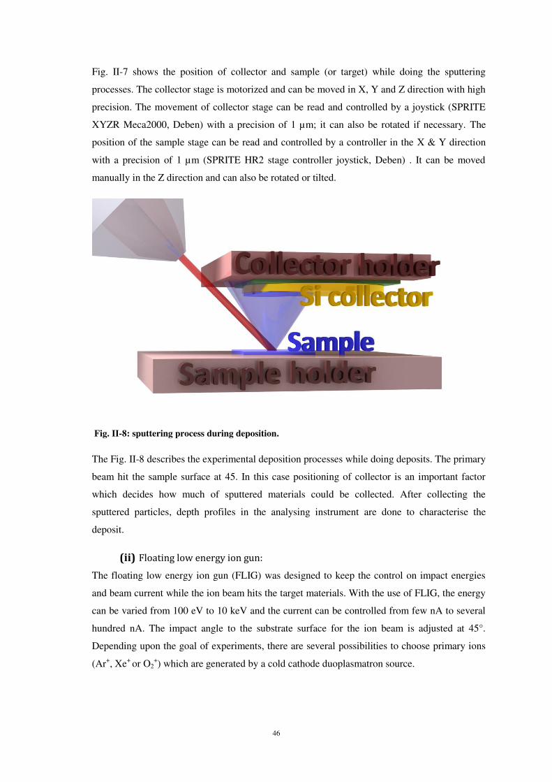
46
Fig. II-7 shows the position of collector and sample (or target) while doing the sputtering
processes. The collector stage is motorized and can be moved in X, Y and Z direction with high
precision. The movement of collector stage can be read and controlled by a joystick (SPRITE
XYZR Meca2000, Deben) with a precision of 1 µm; it can also be rotated if necessary. The
position of the sample stage can be read and controlled by a controller in the X & Y direction
with a precision of 1 µm (SPRITE HR2 stage controller joystick, Deben) . It can be moved
manually in the Z direction and can also be rotated or tilted.
Fig. II-8: sputtering process during deposition.
The Fig. II-8 describes the experimental deposition processes while doing deposits. The primary
beam hit the sample surface at 45. In this case positioning of collector is an important factor
which decides how much of sputtered materials could be collected. After collecting the
sputtered particles, depth profiles in the analysing instrument are done to characterise the
deposit.
(ii) Floating low energy ion gun:
The floating low energy ion gun (FLIG) was designed to keep the control on impact energies
and beam current while the ion beam hits the target materials. With the use of FLIG, the energy
can be varied from 100 eV to 10 keV and the current can be controlled from few nA to several
hundred nA. The impact angle to the substrate surface for the ion beam is adjusted at 45°.
Depending upon the goal of experiments, there are several possibilities to choose primary ions
(Ar+, Xe+ or O2+) which are generated by a cold cathode duoplasmatron source.
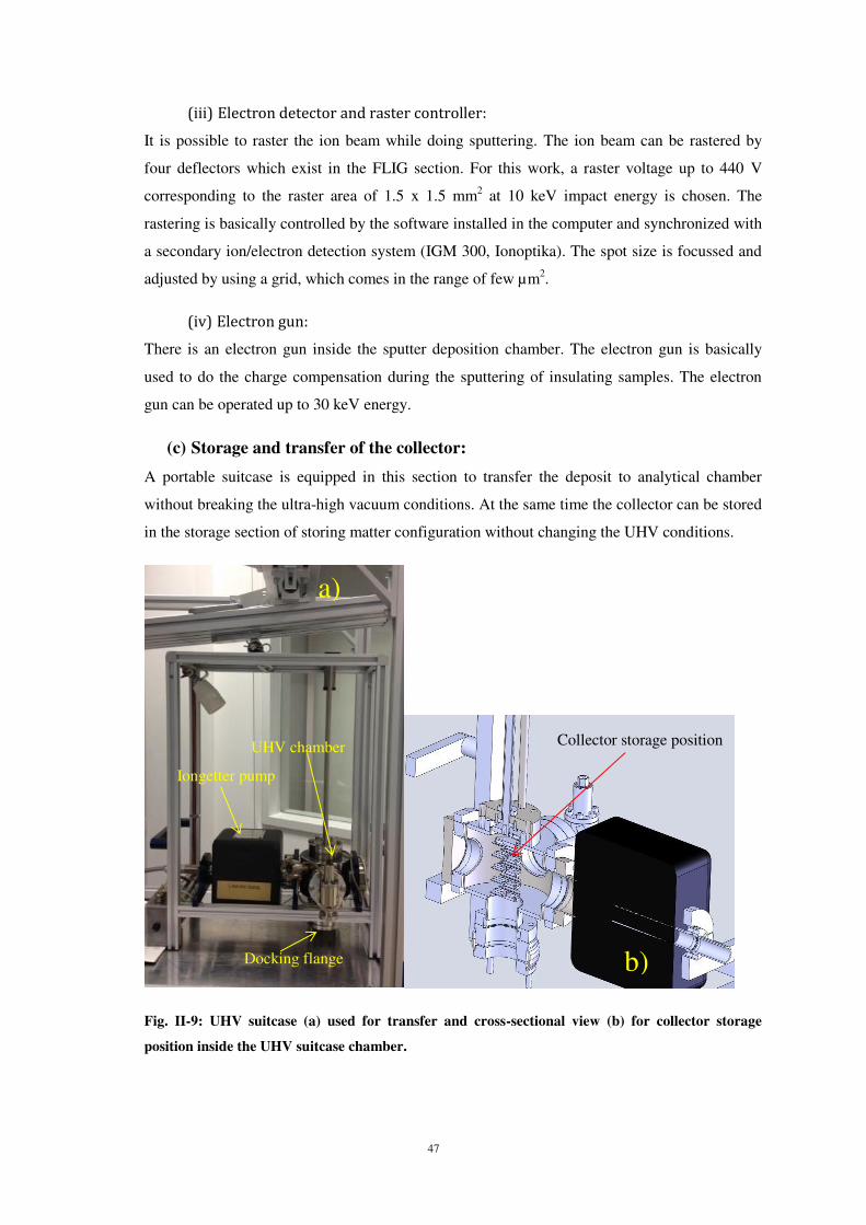
47
(iii) Electron detector and raster controller:
It is possible to raster the ion beam while doing sputtering. The ion beam can be rastered by
four deflectors which exist in the FLIG section. For this work, a raster voltage up to 440 V
corresponding to the raster area of 1.5 x 1.5 mm2 at 10 keV impact energy is chosen. The
rastering is basically controlled by the software installed in the computer and synchronized with
a secondary ion/electron detection system (IGM 300, Ionoptika). The spot size is focussed and
adjusted by using a grid, which comes in the range of few µm2.
(iv) Electron gun:
There is an electron gun inside the sputter deposition chamber. The electron gun is basically
used to do the charge compensation during the sputtering of insulating samples. The electron
gun can be operated up to 30 keV energy.
(c) Storage and transfer of the collector:
A portable suitcase is equipped in this section to transfer the deposit to analytical chamber
without breaking the ultra-high vacuum conditions. At the same time the collector can be stored
in the storage section of storing matter configuration without changing the UHV conditions.
Fig. II-9: UHV suitcase (a) used for transfer and cross-sectional view (b) for collector storage
position inside the UHV suitcase chamber.
a)
b)
UHV chamber Iongetter pump
Docking flange
Collector storage position
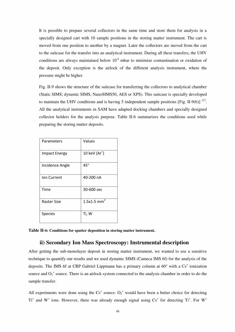
48
It is possible to prepare several collectors in the same time and store them for analysis in a
specially designed cart with 10 sample positions in the storing matter instrument. The cart is
moved from one position to another by a magnet. Later the collectors are moved from the cart
to the suitcase for the transfer into an analytical instrument. During all these transfers, the UHV
conditions are always maintained below 10-8 mbar to minimize contamination or oxidation of
the deposit. Only exception is the airlock of the different analysis instrument, where the
pressure might be higher.
Fig. II-9 shows the structure of the suitcase for transferring the collectors to analytical chamber
(Static SIMS; dynamic SIMS, NanoSIMS50, AES or XPS). This suitcase is specially developed
to maintain the UHV conditions and is having 5 independent sample positions [Fig. II-9(b)] 127.
All the analytical instruments in SAM have adapted docking chambers and specially designed
collector holders for the analysis purpose. Table II-6 summarizes the conditions used while
preparing the storing matter deposits.
Parameters Values
Impact Energy 10 keV (Ar+)
Incidence Angle 45°
Ion Current 40-200 nA
Time 30-600 sec
Raster Size 1.5x1.5 mm2
Species Ti, W
Table II-6: Conditions for sputter deposition in storing matter instrument.
ii) Secondary Ion Mass Spectroscopy: Instrumental description
After getting the sub-monolayer deposit in storing matter instrument, we wanted to use a sensitive
technique to quantify our results and we used dynamic SIMS (Cameca IMS 6f) for the analysis of the
deposits. The IMS 6f at CRP Gabriel Lippmann has a primary column at 60° with a Cs+ ionization
source and O2+ source. There is an airlock system connected to the analysis chamber in order to do the
sample transfer.
All experiments were done using the Cs+ source. O2+ would have been a better choice for detecting
Ti+ and W+ ions. However, there was already enough signal using Cs+ for detecting Ti+. For W+
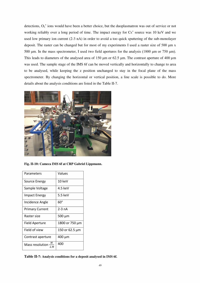
49
detections, O2+ ions would have been a better choice, but the duoplasmatron was out of service or not
working reliably over a long period of time. The impact energy for Cs+ source was 10 keV and we
used low primary ion current (2-3 nA) in order to avoid a too quick sputtering of the sub-monolayer
deposit. The raster can be changed but for most of my experiments I used a raster size of η00 m x
500 m. In the mass spectrometer, I used two field apertures for the analysis (1κ00 m or 7η0 m).
This leads to diameters of the analysed area of 1η0 m or 62.5 m. The contrast aperture of 400 µm
was used. The sample stage of the IMS 6f can be moved vertically and horizontally to change to area
to be analysed, while keeping the z position unchanged to stay in the focal plane of the mass
spectrometer. By changing the horizontal or vertical position, a line scale is possible to do. More
details about the analysis conditions are listed in the Table II-7.
Fig. II-10: Cameca IMS 6f at CRP Gabriel Lippmann.
Parameters Values
Source Energy 10 keV
Sample Voltage 4.5 keV
Impact Energy 5.5 keV
Incidence Angle 60°
Primary Current 2-3 nA
Raster size 500 µm
Field Aperture 1800 or 750 µm
Field of view 150 or 62.5 µm
Contrast aperture 400 µm
Mass resolution 400
Table II-7: Analysis conditions for a deposit analysed in IMS 6f.
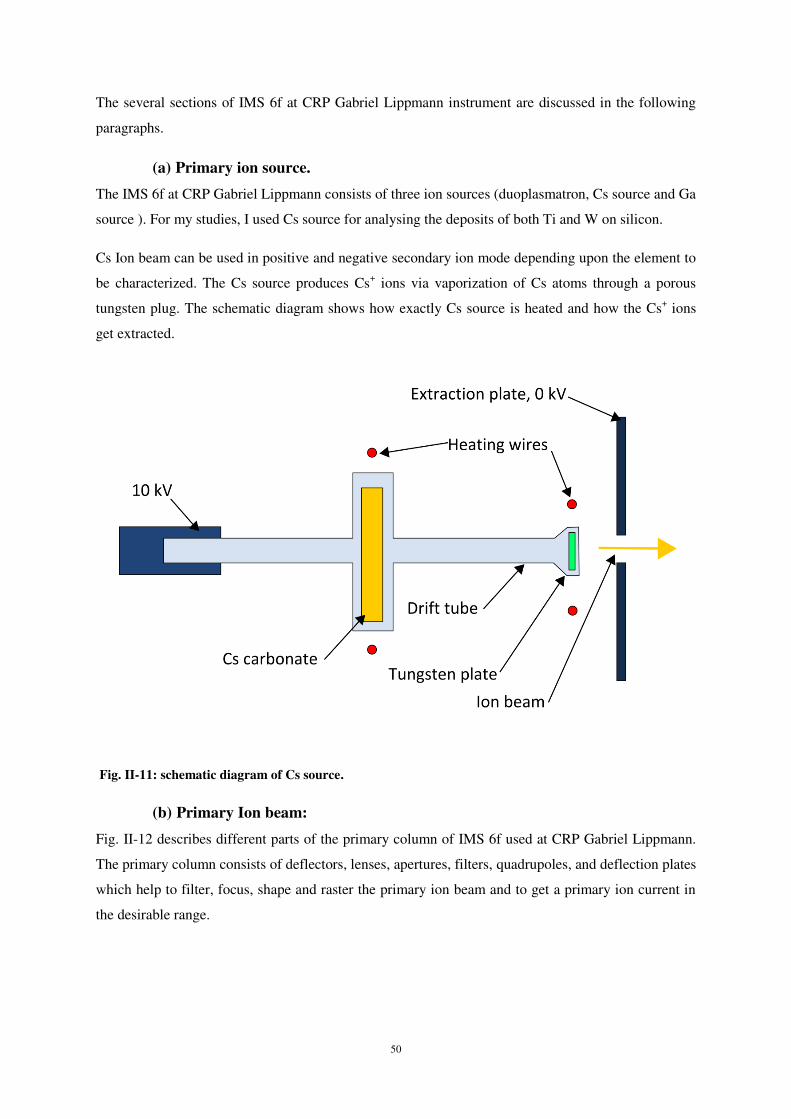
50
The several sections of IMS 6f at CRP Gabriel Lippmann instrument are discussed in the following
paragraphs.
(a) Primary ion source.
The IMS 6f at CRP Gabriel Lippmann consists of three ion sources (duoplasmatron, Cs source and Ga
source ). For my studies, I used Cs source for analysing the deposits of both Ti and W on silicon.
Cs Ion beam can be used in positive and negative secondary ion mode depending upon the element to
be characterized. The Cs source produces Cs+ ions via vaporization of Cs atoms through a porous
tungsten plug. The schematic diagram shows how exactly Cs source is heated and how the Cs+ ions
get extracted.
Fig. II-11: schematic diagram of Cs source.
(b) Primary Ion beam:
Fig. II-12 describes different parts of the primary column of IMS 6f used at CRP Gabriel Lippmann.
The primary column consists of deflectors, lenses, apertures, filters, quadrupoles, and deflection plates
which help to filter, focus, shape and raster the primary ion beam and to get a primary ion current in
the desirable range.
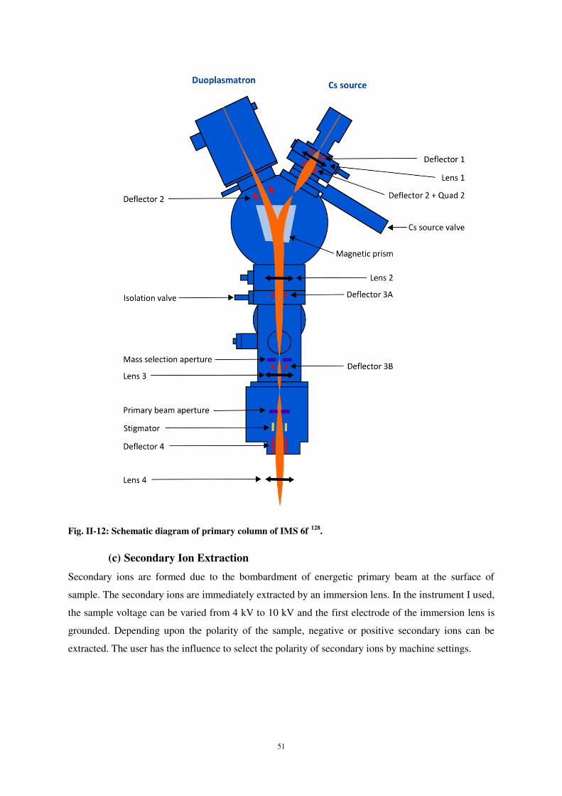
51
Fig. II-12: Schematic diagram of primary column of IMS 6f 128.
(c) Secondary Ion Extraction
Secondary ions are formed due to the bombardment of energetic primary beam at the surface of
sample. The secondary ions are immediately extracted by an immersion lens. In the instrument I used,
the sample voltage can be varied from 4 kV to 10 kV and the first electrode of the immersion lens is
grounded. Depending upon the polarity of the sample, negative or positive secondary ions can be
extracted. The user has the influence to select the polarity of secondary ions by machine settings.
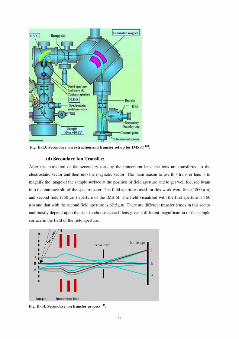
52
Fig. II-13: Secondary ion extraction and transfer set up for IMS 6f 128.
(d) Secondary Ion Transfer:
After the extraction of the secondary ions by the immersion lens, the ions are transferred to the
electrostatic sector and then into the magnetic sector. The main reason to use this transfer lens is to
magnify the image of the sample surface at the position of field aperture and to get well focused beam
into the entrance slit of the spectrometer. The field apertures used for this work were first (1800 µm)
and second field (750 µm) aperture of the IMS 6f. The field visualised with the first aperture is 150
µm and that with the second field aperture is 62.5 µm. There are different transfer lenses in this sector
and mostly depend upon the user to choose as each lens gives a different magnification of the sample
surface in the field of the field aperture.
Fig. II-14: Secondary ion transfer process 128.
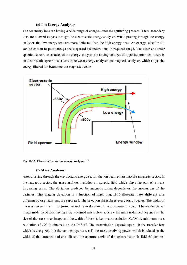
53
(e) Ion Energy Analyser
The secondary ions are having a wide range of energies after the sputtering process. These secondary
ions are allowed to pass through the electrostatic energy analyser. While passing through the energy
analyser, the low energy ions are more deflected than the high energy ones. An energy selection slit
can be chosen to pass through the dispersed secondary ions in required range. The outer and inner
spherical electrode surfaces of the energy analyser are having voltages of opposite polarities. There is
an electrostatic spectrometer lens in between energy analyser and magnetic analyser, which aligns the
energy filtered ion beam into the magnetic sector.
Fig. II-15: Diagram for an ion energy analyser 129.
(f) Mass Analyser:
After crossing through the electrostatic energy sector, the ion beam enters into the magnetic sector. In
the magnetic sector, the mass analyser includes a magnetic field which plays the part of a mass
dispersing prism. The deviation produced by magnetic prism depends on the momentum of the
particles. This angular deviation is a function of mass. Fig. II-16 illustrates how different ions
differing by one mass unit are separated. The selection slit isolates every ionic species. The width of
the mass selection slit is adjusted according to the size of the cross-over image and hence the virtual
image made up of ions having a well-defined mass. How accurate the mass is defined depends on the
size of the cross-over image and the width of the slit, i.e., mass resolution M/M. A minimum mass
resolution of 300 is obtained on the IMS 6f. The transmission depends upon: (i) the transfer lens
which is energized, (ii) the contrast aperture, (iii) the mass resolving power which is related to the
width of the entrance and exit slit and the aperture angle of the spectrometer. In IMS 6f, contrast
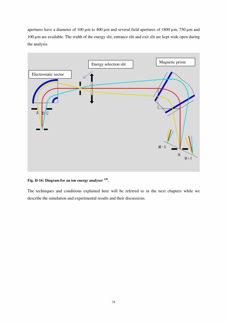
54
apertures have a diameter of 100 µm to 400 µm and several field apertures of 1800 µm, 750 µm and
100 µm are available. The width of the energy slit, entrance slit and exit slit are kept wide open during
the analysis.
Fig. II-16: Diagram for an ion energy analyser 128.
The techniques and conditions explained here will be referred to in the next chapters while we
describe the simulation and experimental results and their discussions.
Magnetic prism Energy selection slit
Electrostatic sector
55
C deposition on Si
“Influence of angle and energy on sticking, deposition and
implantation of carbon atoms on silicon surface has been
investigated for single carbon depositions. Similarly, multiple
carbon depositions have been investigated to observe several
issues regarding deposition and implantation processes, as well
as diffusion mechanism and damage formation.”

56
57
Chapitre 3.
Carbon (C) deposition on Si (100) by
Molecular Dynamics Simulations
1) Introduction: The properties of the materials to be deposited on the surface and the properties of the surface are
very important because it determines the properties of the interface to be formed. In this chapter, the
deposition and sticking of carbon on silicon (100) will be investigated by molecular dynamics
simulations. The main objective to deposit carbon on silicon was to understand the very first steps of
the formation mechanisms of SiC and the sticking of carbon in the sub-monolayer range in the storing
matter instrument 109 using silicon wafers as collector. How and where carbon gets deposited or
implanted, as well as the evolution of the sample composition and structure with increasing carbon
fluence is studied.
In order to understand in detail the atomic scale mechanisms, the carbon-silicon interaction plays an
important role and we use MD simulations with the reactive force field developed by John Kieffer and
co-workers61,62,67 to gain a better understanding how the angle and energy influence the deposition
mechanisms and the formation of SiC compound. This force field allows for the possibility to account
for the breaking and formation of bonds as well as for a dynamic charge transfer between pair of
atoms, which is important for the Si-C system. During the interactions between Si and C, the possible
interactions may occur are Si-Si, Si-C and C-C interactions. The different parameters and their ability
to model silicon carbide, including formation energy of several point defects in these structures, were
already tested previously.
The results for carbon deposition will be discussed in two parts. We start the investigation by
depositing single carbon atoms by MD simulations. The results we get with the Kieffer force field for
single impacts have been compared with the well-tested Erhart-Albe interatomic potential in order to
validate our results. The part with the Erhart-Albe potential has been carried out at the University of
Helsinki. The results have been published in the Journal of Physics;: condensed matter122.
Next, the deposition of multiple carbon atoms will allow for the simulation of the sub-monolayer
deposition process and to understand how and where the carbon atoms deposit.
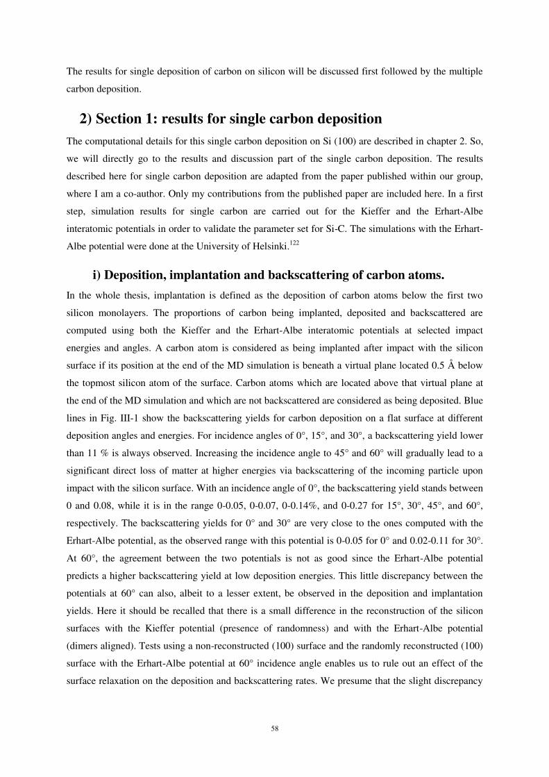
58
The results for single deposition of carbon on silicon will be discussed first followed by the multiple
carbon deposition.
2) Section 1: results for single carbon deposition The computational details for this single carbon deposition on Si (100) are described in chapter 2. So,
we will directly go to the results and discussion part of the single carbon deposition. The results
described here for single carbon deposition are adapted from the paper published within our group,
where I am a co-author. Only my contributions from the published paper are included here. In a first
step, simulation results for single carbon are carried out for the Kieffer and the Erhart-Albe
interatomic potentials in order to validate the parameter set for Si-C. The simulations with the Erhart-
Albe potential were done at the University of Helsinki.122
i) Deposition, implantation and backscattering of carbon atoms.
In the whole thesis, implantation is defined as the deposition of carbon atoms below the first two
silicon monolayers. The proportions of carbon being implanted, deposited and backscattered are
computed using both the Kieffer and the Erhart-Albe interatomic potentials at selected impact
energies and angles. A carbon atom is considered as being implanted after impact with the silicon
surface if its position at the end of the MD simulation is beneath a virtual plane located 0.5 Å below
the topmost silicon atom of the surface. Carbon atoms which are located above that virtual plane at
the end of the MD simulation and which are not backscattered are considered as being deposited. Blue
lines in Fig. III-1 show the backscattering yields for carbon deposition on a flat surface at different
deposition angles and energies. For incidence angles of 0°, 15°, and 30°, a backscattering yield lower
than 11 % is always observed. Increasing the incidence angle to 45° and 60° will gradually lead to a
significant direct loss of matter at higher energies via backscattering of the incoming particle upon
impact with the silicon surface. With an incidence angle of 0°, the backscattering yield stands between
0 and 0.08, while it is in the range 0-0.05, 0-0.07, 0-0.14%, and 0-0.27 for 15°, 30°, 45°, and 60°,
respectively. The backscattering yields for 0° and 30° are very close to the ones computed with the
Erhart-Albe potential, as the observed range with this potential is 0-0.05 for 0° and 0.02-0.11 for 30°.
At 60°, the agreement between the two potentials is not as good since the Erhart-Albe potential
predicts a higher backscattering yield at low deposition energies. This little discrepancy between the
potentials at 60° can also, albeit to a lesser extent, be observed in the deposition and implantation
yields. Here it should be recalled that there is a small difference in the reconstruction of the silicon
surfaces with the Kieffer potential (presence of randomness) and with the Erhart-Albe potential
(dimers aligned). Tests using a non-reconstructed (100) surface and the randomly reconstructed (100)
surface with the Erhart-Albe potential at 60° incidence angle enables us to rule out an effect of the
surface relaxation on the deposition and backscattering rates. We presume that the slight discrepancy
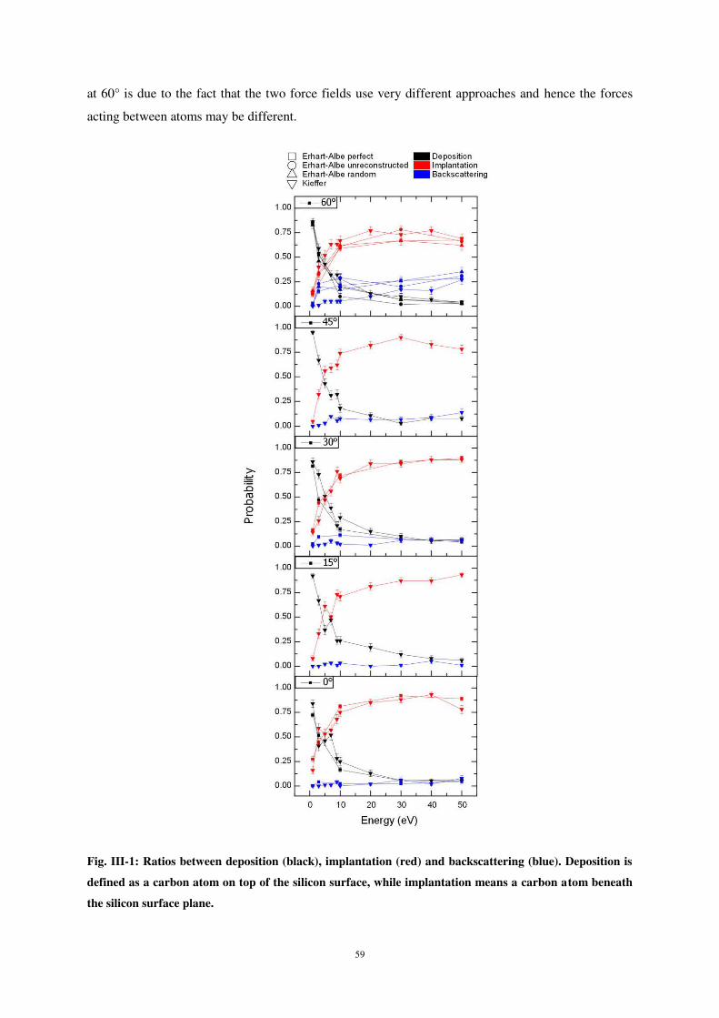
59
at 60° is due to the fact that the two force fields use very different approaches and hence the forces
acting between atoms may be different.
Fig. III-1: Ratios between deposition (black), implantation (red) and backscattering (blue). Deposition is
defined as a carbon atom on top of the silicon surface, while implantation means a carbon atom beneath
the silicon surface plane.
D Erhart-Aibe perfect - Deposit ion 0 Erhart-Aibe unreconstructed - Implantat ion L'-, Erhart-Aibe random - Backscattering \! Kieffer
0.75
0.50
0.25
0.00
1.00
0.75
0.50
0.25
---! --y 0.00
1.00
>- 0.75 ~ .0 ro 0.50 .0
e 0... 0.25
0.00 t 1
1.00
0.75
0.50
0.25
0.00
1.00
0.75
0.50
0.25
0.00
0 10 20 30 40 50
Energy (eV)
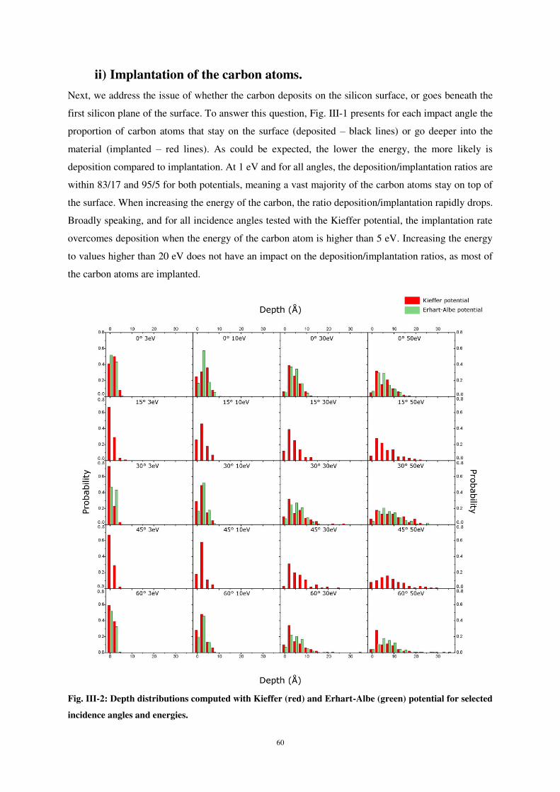
60
ii) Implantation of the carbon atoms.
Next, we address the issue of whether the carbon deposits on the silicon surface, or goes beneath the
first silicon plane of the surface. To answer this question, Fig. III-1 presents for each impact angle the
proportion of carbon atoms that stay on the surface (deposited – black lines) or go deeper into the
material (implanted – red lines). As could be expected, the lower the energy, the more likely is
deposition compared to implantation. At 1 eV and for all angles, the deposition/implantation ratios are
within 83/17 and 95/5 for both potentials, meaning a vast majority of the carbon atoms stay on top of
the surface. When increasing the energy of the carbon, the ratio deposition/implantation rapidly drops.
Broadly speaking, and for all incidence angles tested with the Kieffer potential, the implantation rate
overcomes deposition when the energy of the carbon atom is higher than 5 eV. Increasing the energy
to values higher than 20 eV does not have an impact on the deposition/implantation ratios, as most of
the carbon atoms are implanted.
Fig. III-2: Depth distributions computed with Kieffer (red) and Erhart-Albe (green) potential for selected
incidence angles and energies.
61
In Fig. III-2 the dispersion of deposition depths for selected energies and incidence angles are
presented. Fig. III-3 shows the average depth reached by the carbon projectile for each impact and
incidence angle. The depth is computed by taking the difference in z coordinates of the impact point
on the substrate and of the final configuration of the carbon atom. Backscattered atoms are ignored
whenever averages are computed. The data for both potentials is presented in Fig. III-2 and Fig. III-3
and no major systematic differences can be observed. The higher backscattering yields that have been
observed in Fig. III-1 for deposition at low energies coupled with a 60° incidence angle have no
impact on the depth reached by the carbon. Instead, the largest differences in the implantation depths
between the two potentials are observed for the higher deposition energies at 30° and 60° incidence
angles. These divergences stay within the error bars and are not systematic, since at 50 eV – 60° the
Erhart-Albe potential provides a slightly deeper implantation and at 50eV – 30°, it is the Kieffer
potential that provides the deepest implantation. From Fig. III-2, it can be seen that the shallower
implantation for the Kieffer potential at 50eV – 60° is due to a higher stopping power of the material
at shallow depths. Similarly, the deeper implantation at 50eV – 30° for the Kieffer potential is due to a
tail in the depth distribution extending deeper than for the Erhart-Albe potential.
Fig. III-3: Evolution of the average depth versus the deposition energy as computed using Kieffer and
Erhart-Albe potentials. The depths are computed as the differences in the z coordinates of the impact
location and the final location of the carbon atom.
Looking at Fig. III-3, one can observe that the incidence angle has no influence on the average depth
of the deposited carbon at energies up to 20 eV. The trend in dispersion of depths for the lower half of
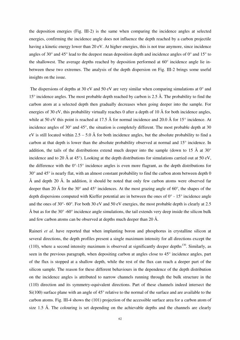
62
the deposition energies (Fig. III-2) is the same when comparing the incidence angles at selected
energies, confirming the incidence angle does not influence the depth reached by a carbon projectile
having a kinetic energy lower than 20 eV. At higher energies, this is not true anymore, since incidence
angles of 30° and 45° lead to the deepest mean deposition depth and incidence angles of 0° and 15° to
the shallowest. The average depths reached by deposition performed at 60° incidence angle lie in-
between these two extremes. The analysis of the depth dispersion on Fig. III-2 brings some useful
insights on the issue.
The dispersions of depths at 30 eV and 50 eV are very similar when comparing simulations at 0° and
15° incidence angles. The most probable depth reached by carbon is 2.5 Å. The probability to find the
carbon atom at a selected depth then gradually decreases when going deeper into the sample. For
energies of 30 eV, this probability virtually reaches 0 after a depth of 10 Å for both incidence angles,
while at 50 eV this point is reached at 17.5 Å for normal incidence and 20.0 Å for 15° incidence. At
incidence angles of 30° and 45°, the situation is completely different. The most probable depth at 30
eV is still located within 2.5 – 5.0 Å for both incidence angles, but the absolute probability to find a
carbon at that depth is lower than the absolute probability observed at normal and 15° incidence. In
addition, the tails of the distributions extend much deeper into the sample (down to 15 Å at 30°
incidence and to 20 Å at 45°). Looking at the depth distributions for simulations carried out at 50 eV,
the difference with the 0°-15° incidence angles is even more flagrant, as the depth distributions for
30° and 45° is nearly flat, with an almost constant probability to find the carbon atom between depth 0
Å and depth 20 Å. In addition, it should be noted that only few carbon atoms were observed far
deeper than 20 Å for the 30° and 45° incidences. At the most grazing angle of 60°, the shapes of the
depth dispersions computed with Kieffer potential are in between the ones of 0° - 15° incidence angle
and the ones of 30°- 60°. For both 30 eV and 50 eV energies, the most probable depth is clearly at 2.5
Å but as for the 30° -60° incidence angle simulations, the tail extends very deep inside the silicon bulk
and few carbon atoms can be observed at depths much deeper than 20 Å.
Raineri et al. have reported that when implanting boron and phosphorus in crystalline silicon at
several directions, the depth profiles present a single maximum intensity for all directions except the
(110), where a second intensity maximum is observed at significantly deeper depths130. Similarly, as
seen in the previous paragraph, when depositing carbon at angles close to 45° incidence angles, part
of the flux is stopped at a shallow depth, while the rest of the flux can reach a deeper part of the
silicon sample. The reason for these different behaviours in the dependence of the depth distribution
on the incidence angles is attributed to narrow channels running through the bulk structure in the
(110) direction and its symmetry-equivalent directions. Part of these channels indeed intersect the
Si(100) surface plane with an angle of 45° relative to the normal of the surface and are available to the
carbon atoms. Fig. III-4 shows the (101) projection of the accessible surface area for a carbon atom of
size 1.5 Å. The colouring is set depending on the achievable depths and the channels are clearly
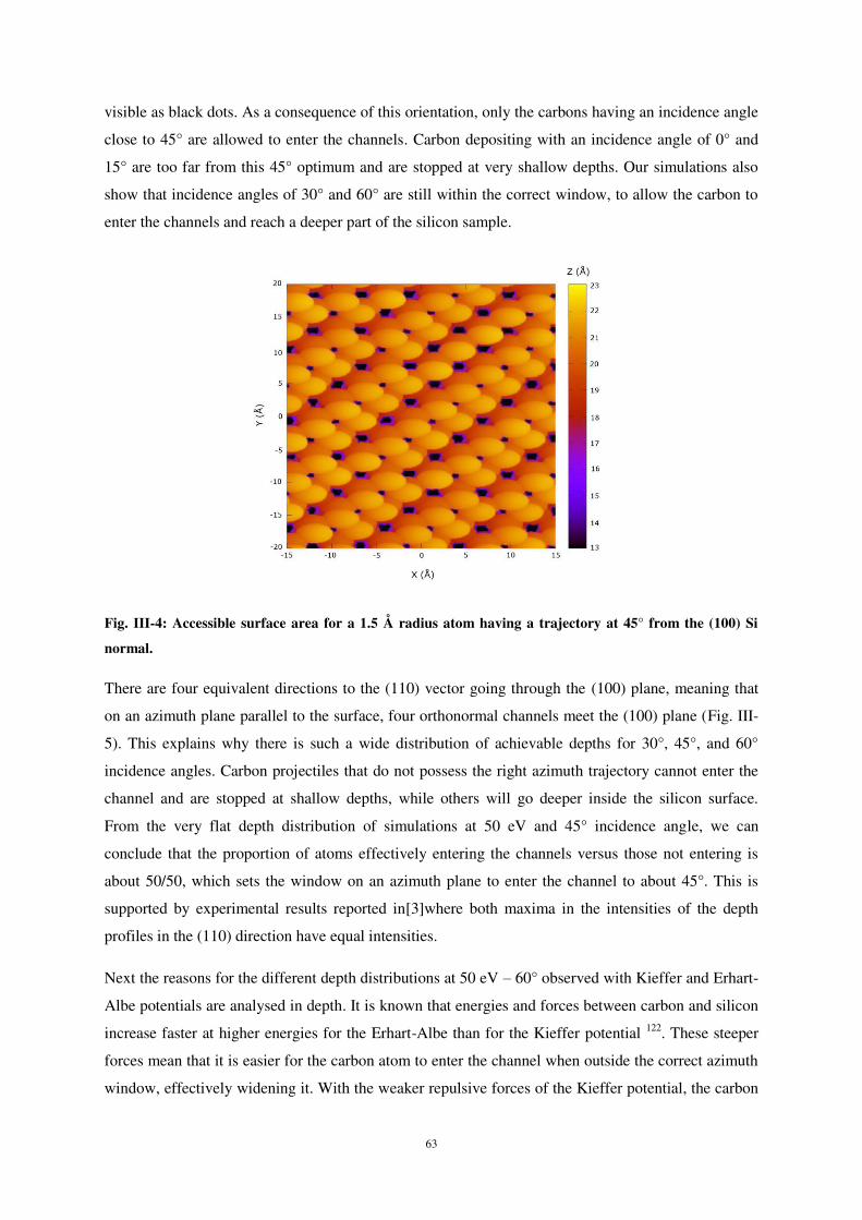
63
visible as black dots. As a consequence of this orientation, only the carbons having an incidence angle
close to 45° are allowed to enter the channels. Carbon depositing with an incidence angle of 0° and
15° are too far from this 45° optimum and are stopped at very shallow depths. Our simulations also
show that incidence angles of 30° and 60° are still within the correct window, to allow the carbon to
enter the channels and reach a deeper part of the silicon sample.
Fig. III-4: Accessible surface area for a 1.5 Å radius atom having a trajectory at 45° from the (100) Si
normal.
There are four equivalent directions to the (110) vector going through the (100) plane, meaning that
on an azimuth plane parallel to the surface, four orthonormal channels meet the (100) plane (Fig. III-
5). This explains why there is such a wide distribution of achievable depths for 30°, 45°, and 60°
incidence angles. Carbon projectiles that do not possess the right azimuth trajectory cannot enter the
channel and are stopped at shallow depths, while others will go deeper inside the silicon surface.
From the very flat depth distribution of simulations at 50 eV and 45° incidence angle, we can
conclude that the proportion of atoms effectively entering the channels versus those not entering is
about 50/50, which sets the window on an azimuth plane to enter the channel to about 45°. This is
supported by experimental results reported in[3]where both maxima in the intensities of the depth
profiles in the (110) direction have equal intensities.
Next the reasons for the different depth distributions at 50 eV – 60° observed with Kieffer and Erhart-
Albe potentials are analysed in depth. It is known that energies and forces between carbon and silicon
increase faster at higher energies for the Erhart-Albe than for the Kieffer potential 122. These steeper
forces mean that it is easier for the carbon atom to enter the channel when outside the correct azimuth
window, effectively widening it. With the weaker repulsive forces of the Kieffer potential, the carbon
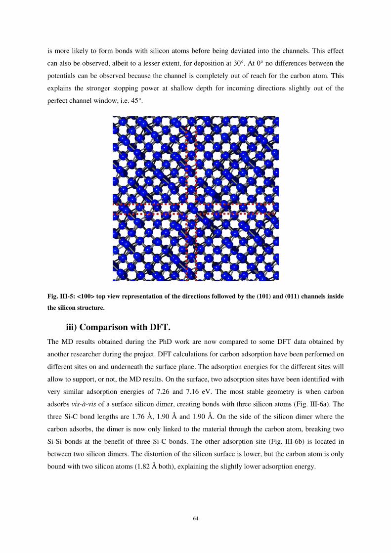
64
is more likely to form bonds with silicon atoms before being deviated into the channels. This effect
can also be observed, albeit to a lesser extent, for deposition at 30°. At 0° no differences between the
potentials can be observed because the channel is completely out of reach for the carbon atom. This
explains the stronger stopping power at shallow depth for incoming directions slightly out of the
perfect channel window, i.e. 45°.
Fig. III-5: <100> top view representation of the directions followed by the (101) and (011) channels inside
the silicon structure.
iii) Comparison with DFT.
The MD results obtained during the PhD work are now compared to some DFT data obtained by
another researcher during the project. DFT calculations for carbon adsorption have been performed on
different sites on and underneath the surface plane. The adsorption energies for the different sites will
allow to support, or not, the MD results. On the surface, two adsorption sites have been identified with
very similar adsorption energies of 7.26 and 7.16 eV. The most stable geometry is when carbon
adsorbs vis-à-vis of a surface silicon dimer, creating bonds with three silicon atoms (Fig. III-6a). The
three Si-C bond lengths are 1.76 Å, 1.90 Å and 1.90 Å. On the side of the silicon dimer where the
carbon adsorbs, the dimer is now only linked to the material through the carbon atom, breaking two
Si-Si bonds at the benefit of three Si-C bonds. The other adsorption site (Fig. III-6b) is located in
between two silicon dimers. The distortion of the silicon surface is lower, but the carbon atom is only
bound with two silicon atoms (1.82 Å both), explaining the slightly lower adsorption energy.
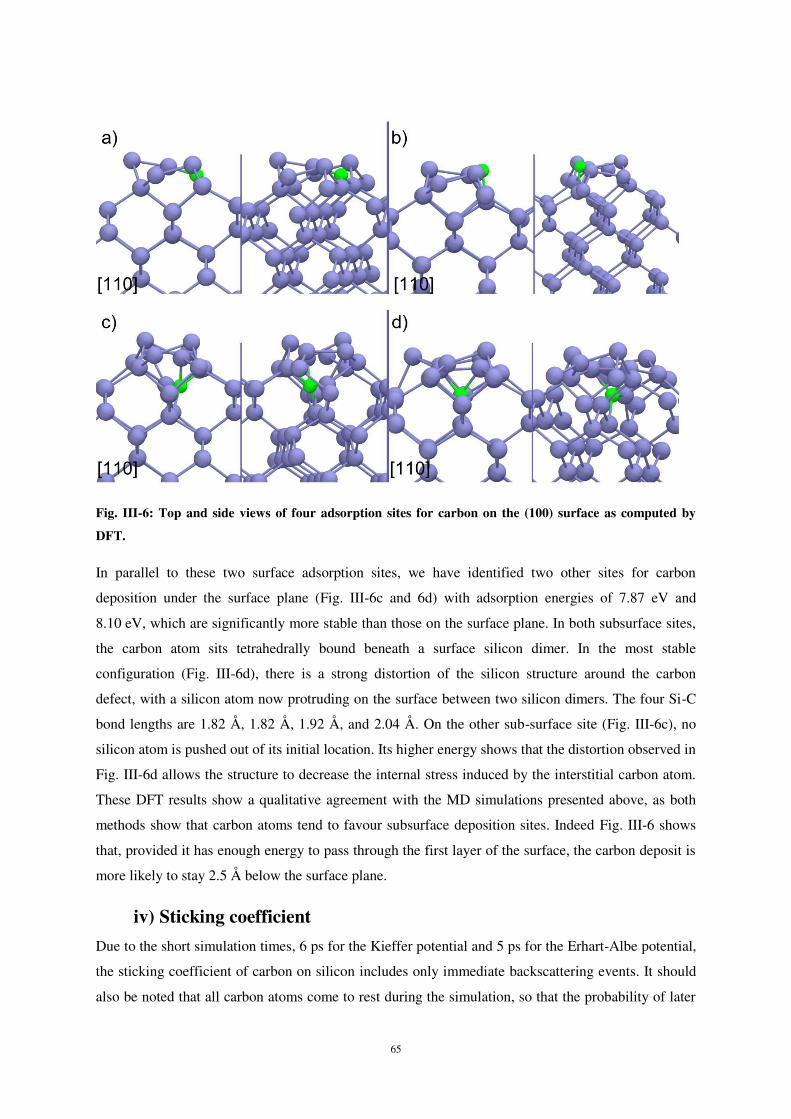
65
Fig. III-6: Top and side views of four adsorption sites for carbon on the (100) surface as computed by
DFT.
In parallel to these two surface adsorption sites, we have identified two other sites for carbon
deposition under the surface plane (Fig. III-6c and 6d) with adsorption energies of 7.87 eV and
8.10 eV, which are significantly more stable than those on the surface plane. In both subsurface sites,
the carbon atom sits tetrahedrally bound beneath a surface silicon dimer. In the most stable
configuration (Fig. III-6d), there is a strong distortion of the silicon structure around the carbon
defect, with a silicon atom now protruding on the surface between two silicon dimers. The four Si-C
bond lengths are 1.82 Å, 1.82 Å, 1.92 Å, and 2.04 Å. On the other sub-surface site (Fig. III-6c), no
silicon atom is pushed out of its initial location. Its higher energy shows that the distortion observed in
Fig. III-6d allows the structure to decrease the internal stress induced by the interstitial carbon atom.
These DFT results show a qualitative agreement with the MD simulations presented above, as both
methods show that carbon atoms tend to favour subsurface deposition sites. Indeed Fig. III-6 shows
that, provided it has enough energy to pass through the first layer of the surface, the carbon deposit is
more likely to stay 2.5 Å below the surface plane.
iv) Sticking coefficient
Due to the short simulation times, 6 ps for the Kieffer potential and 5 ps for the Erhart-Albe potential,
the sticking coefficient of carbon on silicon includes only immediate backscattering events. It should
also be noted that all carbon atoms come to rest during the simulation, so that the probability of later
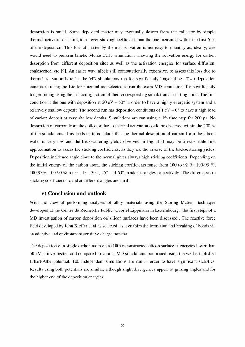
66
desorption is small. Some deposited matter may eventually desorb from the collector by simple
thermal activation, leading to a lower sticking coefficient than the one measured within the first 6 ps
of the deposition. This loss of matter by thermal activation is not easy to quantify as, ideally, one
would need to perform kinetic Monte-Carlo simulations knowing the activation energy for carbon
desorption from different deposition sites as well as the activation energies for surface diffusion,
coalescence, etc [9]. An easier way, albeit still computationally expensive, to assess this loss due to
thermal activation is to let the MD simulations run for significantly longer times. Two deposition
conditions using the Kieffer potential are selected to run the extra MD simulations for significantly
longer timing using the last configuration of their corresponding simulation as starting point. The first
condition is the one with deposition at 50 eV – 60° in order to have a highly energetic system and a
relatively shallow deposit. The second run has deposition conditions of 1 eV – 0° to have a high load
of carbon deposit at very shallow depths. Simulations are run using a 1fs time step for 200 ps. No
desorption of carbon from the collector due to thermal activation could be observed within the 200 ps
of the simulations. This leads us to conclude that the thermal desorption of carbon from the silicon
wafer is very low and the backscattering yields observed in Fig. III-1 may be a reasonable first
approximation to assess the sticking coefficients, as they are the inverse of the backscattering yields.
Deposition incidence angle close to the normal gives always high sticking coefficients. Depending on
the initial energy of the carbon atom, the sticking coefficients range from 100 to 92 %, 100-95 %,
100-93%, 100-90 % for 0°, 15°, 30° , 45° and 60° incidence angles respectively. The differences in
sticking coefficients found at different angles are small.
v) Conclusion and outlook
With the view of performing analyses of alloy materials using the Storing Matter technique
developed at the Centre de Recherche Public- Gabriel Lippmann in Luxembourg, the first steps of a
MD investigation of carbon deposition on silicon surfaces have been discussed . The reactive force
field developed by John Kieffer et al. is selected, as it enables the formation and breaking of bonds via
an adaptive and environment sensitive charge transfer.
The deposition of a single carbon atom on a (100) reconstructed silicon surface at energies lower than
50 eV is investigated and compared to similar MD simulations performed using the well-established
Erhart-Albe potential. 100 independent simulations are run in order to have significant statistics.
Results using both potentials are similar, although slight divergences appear at grazing angles and for
the higher end of the deposition energies.
67
3) Section 2: Results for Continuous Carbon Deposition
i) Introduction
Silicon Carbide (SiC) is a semiconductor material with a wide band gap which has interesting
properties for many applications, including among other high-power and high-frequency electronic
devices 131, nuclear technology, deep-space missions and in the semiconducting industry 132,133. At the
same time, the performances of such devices significantly depend on the defects formed during crystal
growth or ion implantation processes. In order to investigate the influence of the defects on the SiC
film properties, several theoretical and experimental studies have been carried out. Both, the electrical
and physical properties of SiC films, or devices made of SiC, change with the SiC crystalline structure 134. As per example, the fabrication of light emitting diodes depends on the intrinsic defects in Silicon
carbide 135. In order to understand how the material properties depend on growth conditions, a detailed
insight into the sputtering/deposition of carbon materials on silicon substrates is of key importance for
thin film growth via plasma deposition techniques and sputter deposition.
In this section of carbon deposition on silicon, we describe the deposition of multiple carbon atoms on
a crystalline silicon (Si) surface modelled at 1, 5, 10, 20, 30 eV energies with initial directions of 0°,
30°, 45° and 60° to the normal of the silicon surface by using molecular dynamics simulations
combined with the afore-described force field that includes bond breaking and formation. In this
section we use the MD simulations to investigate how continuous or multiple carbon deposition on the
silicon surface may influence substrate amorphization and carbon implantation mechanism as
compared to what was observed on crystalline and amorphous silicon surfaces. These simulations
allow for atomic scale insights into the deposition mechanisms and an easier comparison with
experimental observations. The results, including distributions of implantation depth, carbon
concentrations, sticking coefficients, radial distribution function, angular distribution function and
coordination are compared for different incidence angles, energies and fluences. Due to the deposition
of carbon inside the silicon structure, silicon - carbon compound starts to form. The crystalline
structures have been investigated for different conditions to get a better understanding of the
damaging and growth mechanisms. It is found that a lot of damage is accumulated in the area of
deposition near to the surface but underneath the surface the silicon has still a more crystalline
structure. The variation of the silicon structure slightly depends on the angle of incidence. For the
conditions used for these simulations, the sticking probability is always high and varies between 95%
and 100%, which can be attributed to the high affinity of carbon for silicon.
ii) Results and discussion
The results for continuous carbon deposition have been analysed in three approaches to observe the
influence of energy, angle and fluence of the incoming carbon atoms on the deposition mechanisms.
First, the angular influence on deposition and implantation mechanism at a constant energy of 5 eV is
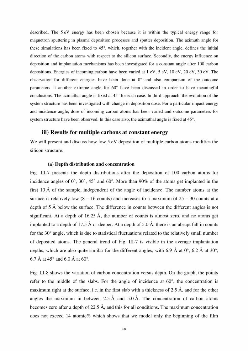
68
described. The 5 eV energy has been chosen because it is within the typical energy range for
magnetron sputtering in plasma deposition processes and sputter deposition. The azimuth angle for
these simulations has been fixed to 45°, which, together with the incident angle, defines the initial
direction of the carbon atoms with respect to the silicon surface. Secondly, the energy influence on
deposition and implantation mechanisms has been investigated for a constant angle after 100 carbon
depositions. Energies of incoming carbon have been varied at 1 eV, 5 eV, 10 eV, 20 eV, 30 eV. The
observation for different energies have been done at 0° and also comparison of the outcome
parameters at another extreme angle for 60° have been discussed in order to have meaningful
conclusions. The azimuthal angle is fixed at 45° for each case. In third approach, the evolution of the
system structure has been investigated with change in deposition dose. For a particular impact energy
and incidence angle, dose of incoming carbon atoms has been varied and outcome parameters for
system structure have been observed. In this case also, the azimuthal angle is fixed at 45°.
iii) Results for multiple carbons at constant energy
We will present and discuss how low 5 eV deposition of multiple carbon atoms modifies the
silicon structure.
(a) Depth distribution and concentration
Fig. III-7 presents the depth distributions after the deposition of 100 carbon atoms for
incidence angles of 0°, 30°, 45° and 60°. More than 90% of the atoms get implanted in the
first 10 Å of the sample, independent of the angle of incidence. The number atoms at the
surface is relatively low (8 – 16 counts) and increases to a maximum of 25 – 30 counts at a
depth of 5 Å below the surface. The difference in counts between the different angles is not
significant. At a depth of 16.25 Å, the number of counts is almost zero, and no atoms get
implanted to a depth of 17.5 Å or deeper. At a depth of 5.0 Å, there is an abrupt fall in counts
for the 30° angle, which is due to statistical fluctuations related to the relatively small number
of deposited atoms. The general trend of Fig. III-7 is visible in the average implantation
depths, which are also quite similar for the different angles, with 6.9 Å at 0°, 6.2 Å at 30°,
6.7 Å at 45° and 6.0 Å at 60°.
Fig. III-8 shows the variation of carbon concentration versus depth. On the graph, the points
refer to the middle of the slabs. For the angle of incidence at 60°, the concentration is
maximum right at the surface, i.e. in the first slab with a thickness of 2.5 Å, and for the other
angles the maximum in between 2.5 Å and 5.0 Å. The concentration of carbon atoms
becomes zero after a depth of 22.5 Å, and this for all conditions. The maximum concentration
does not exceed 14 atomic% which shows that we model only the beginning of the film
69
growth and that the concentrations are far from a stoichiometric carbide. Apparent
contradictions between Fig. III-7 and Fig. III-8, like higher C surface concentration for an
incidence angle of 60° versus highest counts for carbon atoms at 30° for the depth
distribution is due to changing number of atoms in the topmost slabs. This is due to slight
roughening of the surface as well as density variations in the topmost slab due to damage
formation. This effect is not visible in Fig. III-7. In general, Fig. III-8 shows that more
grazing incidence leads to higher surface concentrations. The apparent slightly shallower
implantation depth at 60° might be not relevant because of the small difference to the other
incidence angles.
Fig. III-7: Depth distribution of implanted atoms for the incidence angles of 0°, 30°, 45° and 60°.
Fig. III-8: Variation of the concentration of the carbon atoms with depth for the deposition of 100 C on a
Si(100) surface. The data is shown for the 4 incidence angles.
0 5 10 15 20 25 30 35 40
0
2
4
6
8
10
12
14
Con
cent
ratio
n (%
)
Depth (Å)
C, 0° C, 30° C, 45° C, 60°
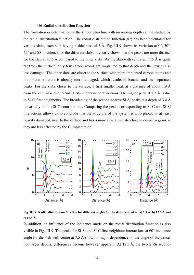
70
(b) Radial distribution function
The formation or deformation of the silicon structure with increasing depth can be studied by
the radial distribution function. The radial distribution function g(r) has been calculated for
various slabs, each slab having a thickness of 5 Å. Fig. III-9 shows its variation at 0°, 30°,
45° and 60° incidence for the different slabs. It clearly shows that the peaks are more distinct
for the slab at 17.5 Å compared to the other slabs. As the slab with centre at 17.5 Å is quite
far from the surface, only few carbon atoms get implanted to that depth and the structure is
less damaged. The other slabs are closer to the surface with more implanted carbon atoms and
the silicon structure is already more damaged, which results in broader and less separated
peaks. For the slabs closer to the surface, a first smaller peak at a distance of about 1.9 Å
from the central is due to Si-C first-neighbour contributions. The higher peak at 2.3 Å is due
to Si-Si first neighbours. The broadening of the second-nearest Si-Si peaks at a depth of 3.4 Å
is partially due to Si-C contributions. Comparing the peaks corresponding to Si-C and Si-Si
interactions allows us to conclude that the structure of the system is amorphous, or at least
heavily damaged, near to the surface and has a more crystalline structure in deeper regions as
they are less affected by the C implantation.
Fig. III-9: Radial distribution function for different angles for the slabs centred on a) 7.5 Å, b) 12.5 Å and
c) 17.5 Å.
In addition, an influence of the incidence angle on the radial distribution function is also
visible in Fig. III-9. The peaks for Si-Si and Si-C first-neighbour interactions at 60° incidence
angle for the slab with centre at 7.5 Å show no major dependence on the angle of incidence.
For larger depths, differences become however apparent. At 12.5 Å, the two Si-Si second-
0 2 4 6 80
5
10
15
Si-S
i nea
rest
neig
hbou
rs
gr
Distance (Å)
0° 30° 45° 60°
7,5 Å
a)
Si-C
nea
rest
neig
hbou
rs
0 2 4 6 80
2
4
6
8
10
12
14
16
18
12,5 Å
Distance (Å)
0° 30° 45° 60°
b)
0 2 4 6 80
5
10
15
20
25
Si-S
i 3rd
near
est
neig
hbou
rs
Distance (Å)
0° 30° 45° 60°
17,5 Åc)S
i-Si 2
nd ne
ares
tne
ighb
ours
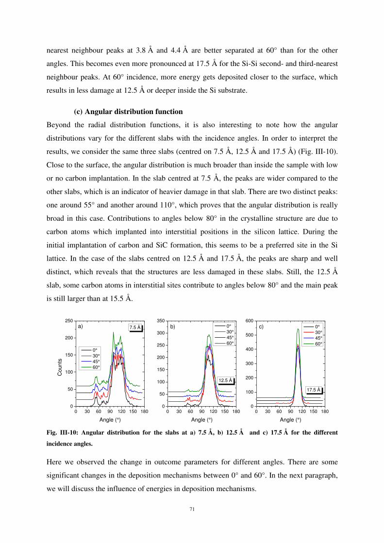
71
nearest neighbour peaks at 3.8 Å and 4.4 Å are better separated at 60° than for the other
angles. This becomes even more pronounced at 17.5 Å for the Si-Si second- and third-nearest
neighbour peaks. At 60° incidence, more energy gets deposited closer to the surface, which
results in less damage at 12.5 Å or deeper inside the Si substrate.
(c) Angular distribution function
Beyond the radial distribution functions, it is also interesting to note how the angular
distributions vary for the different slabs with the incidence angles. In order to interpret the
results, we consider the same three slabs (centred on 7.5 Å, 12.5 Å and 17.5 Å) (Fig. III-10).
Close to the surface, the angular distribution is much broader than inside the sample with low
or no carbon implantation. In the slab centred at 7.5 Å, the peaks are wider compared to the
other slabs, which is an indicator of heavier damage in that slab. There are two distinct peaks:
one around 55° and another around 110°, which proves that the angular distribution is really
broad in this case. Contributions to angles below 80° in the crystalline structure are due to
carbon atoms which implanted into interstitial positions in the silicon lattice. During the
initial implantation of carbon and SiC formation, this seems to be a preferred site in the Si
lattice. In the case of the slabs centred on 12.5 Å and 17.5 Å, the peaks are sharp and well
distinct, which reveals that the structures are less damaged in these slabs. Still, the 12.5 Å
slab, some carbon atoms in interstitial sites contribute to angles below 80° and the main peak
is still larger than at 15.5 Å.
Fig. III-10: Angular distribution for the slabs at a) 7.5 Å, b) 12.5 Å and c) 17.5 Å for the different
incidence angles.
Here we observed the change in outcome parameters for different angles. There are some
significant changes in the deposition mechanisms between 0° and 60°. In the next paragraph,
we will discuss the influence of energies in deposition mechanisms.
0 30 60 90 120 150 1800
50
100
150
200
2507.5 Å
Cou
nts
Angle (°)
0° 30° 45° 60°
a)
0 30 60 90 120 150 1800
100
200
300
400
500
600
Angle (°)
0° 30° 45° 60°
c)
17.5 Å
0 30 60 90 120 150 1800
50
100
150
200
250
300
350
Angle (°)
0° 30° 45° 60°
b)
12.5 Å
72
iv) Results for continuous C deposition at constant angle for different
energies
Previously, we observed how the change in angles influences different mechanisms for
continuous carbon deposition at a constant energy. In this section, we investigate how it
influences several parameters (radial distribution function, depth distribution, angular
distribution function, coordination, concentration) for continuous carbon deposition while the
impact energies of incoming carbon have been changed for a constant angle. Like for the
previous section, the results have been analysed after 100 carbon depositions. The results
have been analysed first at a constant angle of 0° for several energies (1 eV, 5 eV, 20 eV, 30
eV) and also at 60° for the same energy variations. Two constant angles are chosen to verify
if there are significant contributions of angles while the energies are varied to study the
outcome parameters. For both cases, the azimuthal angle is fixed at 45°. In the following
paragraphs we will discuss the outcome of continuous carbon depositions by calculating the
parameters such as radial distribution function, depth distribution, coordination, angular
distribution function, and concentration successively for a constant angle at different
energies.
(a) Radial Distribution Function
The outcome of different structures formed during continuous carbon depositions and
implantations with increasing depth and energy can be studied and explained by the radial
distribution functions. The radial distribution function g(r) has been calculated for various
slabs, each slab having a thickness of 5 Å. Fig. III-11 shows its variation at 1 eV, 5 eV, 20 eV
and 30 eV for different slabs at 0° incidence angle while the azimuthal angle is fixed at 45°.
The peaks are more distinct for the slab at 12.5 Å compared to the other slabs. As the slab
with centre at 12.5 Å is quite far from the surface, only few carbon atoms get implanted to
that depth and the silicon structure is less damaged. The other slabs which are closer to the
surface are already damaged due to the excess number of presence of carbon atoms than the
available lattice sites. For the slabs closer to the surface, it can be observed that there is a first
smaller peak at a distance of about 1.9 Å from the central. This is due to Si-C first-neighbour
contributions. The higher peak at 2.3 Å from the central is due to Si-Si first neighbours. The
peaks corresponding to Si-C and Si-Si interactions give ideas about the structure of the
system. Now we will investigate how energy can influence the system structure by observing
variations in radial distribution function as depicted in Fig. III-11. For the slab with centre at
2.5 Å, the peaks for Si-C first-neighbour at a distance about 1.9 Å for 1 eV have higher
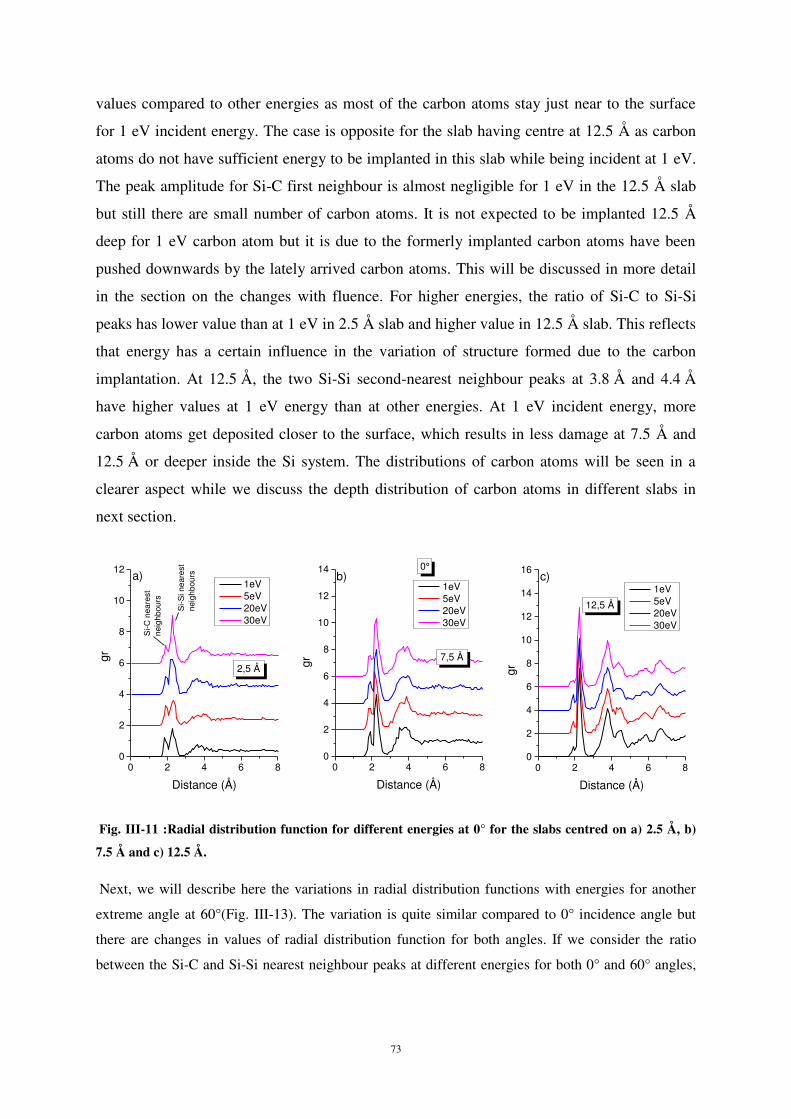
73
values compared to other energies as most of the carbon atoms stay just near to the surface
for 1 eV incident energy. The case is opposite for the slab having centre at 12.5 Å as carbon
atoms do not have sufficient energy to be implanted in this slab while being incident at 1 eV.
The peak amplitude for Si-C first neighbour is almost negligible for 1 eV in the 12.5 Å slab
but still there are small number of carbon atoms. It is not expected to be implanted 12.5 Å
deep for 1 eV carbon atom but it is due to the formerly implanted carbon atoms have been
pushed downwards by the lately arrived carbon atoms. This will be discussed in more detail
in the section on the changes with fluence. For higher energies, the ratio of Si-C to Si-Si
peaks has lower value than at 1 eV in 2.5 Å slab and higher value in 12.5 Å slab. This reflects
that energy has a certain influence in the variation of structure formed due to the carbon
implantation. At 12.5 Å, the two Si-Si second-nearest neighbour peaks at 3.8 Å and 4.4 Å
have higher values at 1 eV energy than at other energies. At 1 eV incident energy, more
carbon atoms get deposited closer to the surface, which results in less damage at 7.5 Å and
12.5 Å or deeper inside the Si system. The distributions of carbon atoms will be seen in a
clearer aspect while we discuss the depth distribution of carbon atoms in different slabs in
next section.
Fig. III-11 :Radial distribution function for different energies at 0° for the slabs centred on a) 2.5 Å, b)
7.5 Å and c) 12.5 Å.
Next, we will describe here the variations in radial distribution functions with energies for another
extreme angle at 60°(Fig. III-13). The variation is quite similar compared to 0° incidence angle but
there are changes in values of radial distribution function for both angles. If we consider the ratio
between the Si-C and Si-Si nearest neighbour peaks at different energies for both 0° and 60° angles,
0 2 4 6 80
2
4
6
8
10
12
14
16
12,5 Å
c)
gr
Distance (Å)
1eV 5eV 20eV 30eV
0 2 4 6 80
2
4
6
8
10
12
14 0°b)
7,5 Å
gr
Distance (Å)
1eV 5eV 20eV 30eV
0 2 4 6 80
2
4
6
8
10
12a)
2,5 Å
Si-S
i nea
rest
neig
hbou
rs
Si-C
nea
rest
neig
hbou
rs
gr
Distance (Å)
1eV 5eV 20eV 30eV
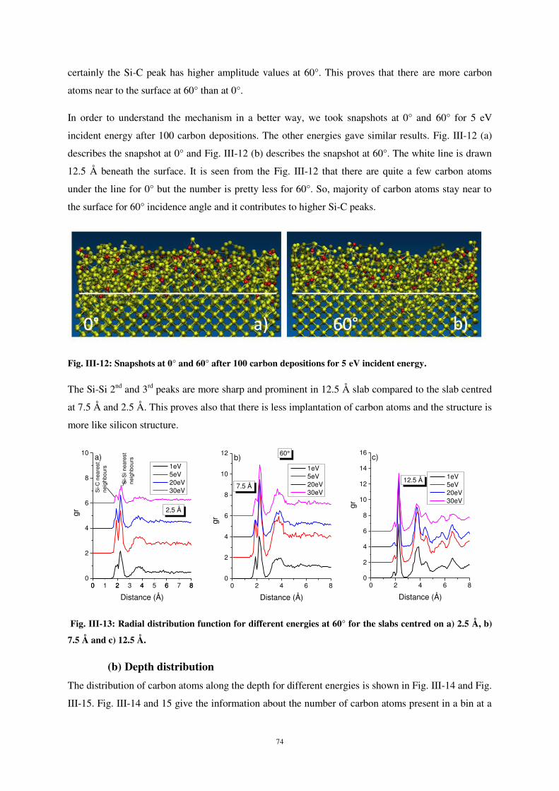
74
certainly the Si-C peak has higher amplitude values at 60°. This proves that there are more carbon
atoms near to the surface at 60° than at 0°.
In order to understand the mechanism in a better way, we took snapshots at 0° and 60° for 5 eV
incident energy after 100 carbon depositions. The other energies gave similar results. Fig. III-12 (a)
describes the snapshot at 0° and Fig. III-12 (b) describes the snapshot at 60°. The white line is drawn
12.5 Å beneath the surface. It is seen from the Fig. III-12 that there are quite a few carbon atoms
under the line for 0° but the number is pretty less for 60°. So, majority of carbon atoms stay near to
the surface for 60° incidence angle and it contributes to higher Si-C peaks.
Fig. III-12: Snapshots at 0° and 60° after 100 carbon depositions for 5 eV incident energy.
The Si-Si 2nd and 3rd peaks are more sharp and prominent in 12.5 Å slab compared to the slab centred
at 7.5 Å and 2.5 Å. This proves also that there is less implantation of carbon atoms and the structure is
more like silicon structure.
Fig. III-13: Radial distribution function for different energies at 60° for the slabs centred on a) 2.5 Å, b)
7.5 Å and c) 12.5 Å.
(b) Depth distribution
The distribution of carbon atoms along the depth for different energies is shown in Fig. III-14 and Fig.
III-15. Fig. III-14 and 15 give the information about the number of carbon atoms present in a bin at a
0 2 4 6 80
2
4
6
8
10
12
14
16
12.5 Å
c)
gr
Distance (Å)
1eV 5eV 20eV 30eV
0 2 4 6 80
2
4
6
8
10
12 60°
7.5 Å
b)
gr
Distance (Å)
1eV 5eV 20eV 30eV
00 1 22 3 44 5 66 7 880
2
4
6
8
10a)
Si-S
i nea
rest
neig
hbou
rs
Si-C
nea
rest
neig
hbou
rs
2,5 Ågr
Distance (Å)
1eV 5eV 20eV 30eV
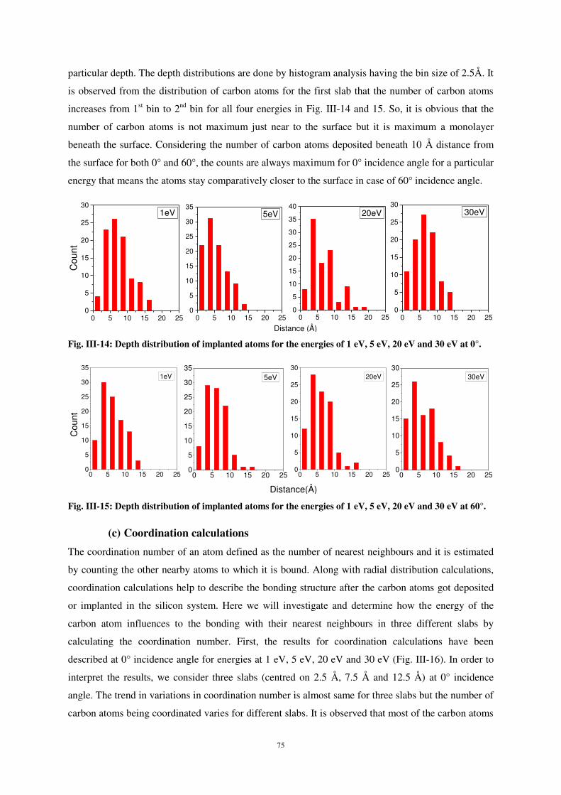
75
particular depth. The depth distributions are done by histogram analysis having the bin size of 2.5Å. It
is observed from the distribution of carbon atoms for the first slab that the number of carbon atoms
increases from 1st bin to 2nd bin for all four energies in Fig. III-14 and 15. So, it is obvious that the
number of carbon atoms is not maximum just near to the surface but it is maximum a monolayer
beneath the surface. Considering the number of carbon atoms deposited beneath 10 Å distance from
the surface for both 0° and 60°, the counts are always maximum for 0° incidence angle for a particular
energy that means the atoms stay comparatively closer to the surface in case of 60° incidence angle.
Fig. III-14: Depth distribution of implanted atoms for the energies of 1 eV, 5 eV, 20 eV and 30 eV at 0°.
Fig. III-15: Depth distribution of implanted atoms for the energies of 1 eV, 5 eV, 20 eV and 30 eV at 60°.
(c) Coordination calculations
The coordination number of an atom defined as the number of nearest neighbours and it is estimated
by counting the other nearby atoms to which it is bound. Along with radial distribution calculations,
coordination calculations help to describe the bonding structure after the carbon atoms got deposited
or implanted in the silicon system. Here we will investigate and determine how the energy of the
carbon atom influences to the bonding with their nearest neighbours in three different slabs by
calculating the coordination number. First, the results for coordination calculations have been
described at 0° incidence angle for energies at 1 eV, 5 eV, 20 eV and 30 eV (Fig. III-16). In order to
interpret the results, we consider three slabs (centred on 2.5 Å, 7.5 Å and 12.5 Å) at 0° incidence
angle. The trend in variations in coordination number is almost same for three slabs but the number of
carbon atoms being coordinated varies for different slabs. It is observed that most of the carbon atoms
0 5 10 15 20 250
5
10
15
20
25
30
Cou
nt
1eV
0 5 10 15 20 250
5
10
15
20
25
30
30eV
0 5 10 15 20 250
5
10
15
20
25
30
35
40
Distance (Å)
20eV
0 5 10 15 20 250
5
10
15
20
25
30
35
5eV
0 5 10 15 20 250
5
10
15
20
25
30
30eV
0 5 10 15 20 250
5
10
15
20
25
30
Distance(Å)
20eV
0 5 10 15 20 250
5
10
15
20
25
30
35
5eV
0 5 10 15 20 250
5
10
15
20
25
30
35
Cou
nt
1eV
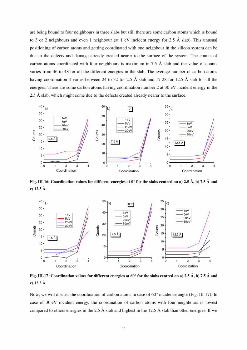
76
are being bound to four neighbours in three slabs but still there are some carbon atoms which is bound
to 3 or 2 neighbours and even 1 neighbour (at 1 eV incident energy for 2.5 Å slab). This unusual
positioning of carbon atoms and getting coordinated with one neighbour in the silicon system can be
due to the defects and damage already created nearer to the surface of the system. The counts of
carbon atoms coordinated with four neighbours is maximum in 7.5 Å slab and the value of counts
varies from 46 to 48 for all the different energies in the slab. The average number of carbon atoms
having coordination 4 varies between 24 to 32 for 2.5 Å slab and 17-28 for 12.5 Å slab for all the
energies. There are some carbon atoms having coordination number 2 at 30 eV incident energy in the
2.5 Å slab, which might come due to the defects created already nearer to the surface.
Fig. III-16: Coordination values for different energies at 0° for the slabs centred on a) 2.5 Å, b) 7.5 Å and
c) 12.5 Å.
Fig. III-17 :Coordination values for different energies at 60° for the slabs centred on a) 2.5 Å, b) 7.5 Å and
c) 12.5 Å.
Now, we will discuss the coordination of carbon atoms in case of 60° incidence angle (Fig. III-17). In
case of 30 eV incident energy, the coordination of carbon atoms with four neighbours is lowest
compared to others energies in the 2.5 Å slab and highest in the 12.5 Å slab than other energies. If we
0 1 2 3 40
5
10
15
20
25
30
35c)
12,5 Å
Cou
nts
Coordination
1eV 5eV 20eV 30eV
0 1 2 3 40
10
20
30
40
50
600°b)
7,5 ÅCou
nts
Coordination
1eV 5eV 20eV 30eV
0 1 2 3 40
5
10
15
20
25
30
35
40a)
2,5 ÅCou
nts
Coordination
1eV 5eV 20eV 30eV
0 1 2 3 40
5
10
15
20
25
30
35c)
12,5 ÅCou
nts
Coordination
1eV 5eV 20eV 30eV
0 1 2 3 40
10
20
30
40
5060°b)
7,5 ÅCou
nts
Coordination
1eV 5eV 20eV 30eV
0 1 2 3 40
5
10
15
20
25
30
35
40 a)
2,5 Å
Cou
nts
Coordination
1eV 5eV 20eV 30eV
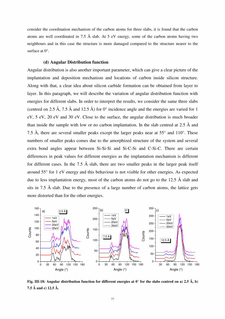
77
consider the coordination mechanism of the carbon atoms for three slabs, it is found that the carbon
atoms are well coordinated in 7.5 Å slab. At 5 eV energy, some of the carbon atoms having two
neighbours and in this case the structure is more damaged compared to the structure nearer to the
surface at 0°.
(d) Angular Distribution function
Angular distribution is also another important parameter, which can give a clear picture of the
implantation and deposition mechanism and locations of carbon inside silicon structure.
Along with that, a clear idea about silicon carbide formation can be obtained from layer to
layer. In this paragraph, we will describe the variation of angular distribution function with
energies for different slabs. In order to interpret the results, we consider the same three slabs
(centred on 2.5 Å, 7.5 Å and 12.5 Å) for 0° incidence angle and the energies are varied for 1
eV, 5 eV, 20 eV and 30 eV. Close to the surface, the angular distribution is much broader
than inside the sample with low or no carbon implantation. In the slab centred at 2.5 Å and
7.5 Å, there are several smaller peaks except the larger peaks near at 55° and 110°. These
numbers of smaller peaks comes due to the amorphized structure of the system and several
extra bond angles appear between Si-Si-Si and Si-C-Si and C-Si-C. There are certain
differences in peak values for different energies as the implantation mechanism is different
for different cases. In the 7.5 Å slab, there are two smaller peaks in the larger peak itself
around 55° for 1 eV energy and this behaviour is not visible for other energies. As expected
due to less implantation energy, most of the carbon atoms do not go to the 12.5 Å slab and
sits in 7.5 Å slab. Due to the presence of a large number of carbon atoms, the lattice gets
more distorted than for the other energies.
Fig. III-18: Angular distribution function for different energies at 0° for the slabs centred on a) 2.5 Å, b)
7.5 Å and c) 12.5 Å.
30 60 90 120 150 1800
50
100
150
200
250
300
350c)
12.5 ÅCou
nts
Angle (°)
1eV 5eV 20eV 30eV
0 30 60 90 120 150 1800
50
100
150
200
2500°b)
7.5 ÅCou
nts
Angle (°)
1eV 5eV 20eV 30eV
0 30 60 90 120 150 1800
20
40
60
80
100
120
140
160a)
a)
2.5 Å
Cou
nts
Angle (°)
1eV 5eV 20eV 30eV
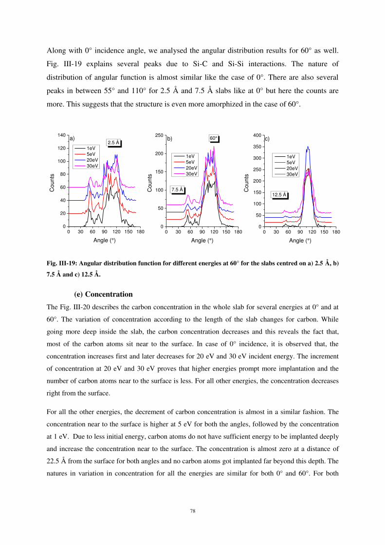
78
Along with 0° incidence angle, we analysed the angular distribution results for 60° as well.
Fig. III-19 explains several peaks due to Si-C and Si-Si interactions. The nature of
distribution of angular function is almost similar like the case of 0°. There are also several
peaks in between 55° and 110° for 2.5 Å and 7.5 Å slabs like at 0° but here the counts are
more. This suggests that the structure is even more amorphized in the case of 60°.
Fig. III-19: Angular distribution function for different energies at 60° for the slabs centred on a) 2.5 Å, b)
7.5 Å and c) 12.5 Å.
(e) Concentration
The Fig. III-20 describes the carbon concentration in the whole slab for several energies at 0° and at
60°. The variation of concentration according to the length of the slab changes for carbon. While
going more deep inside the slab, the carbon concentration decreases and this reveals the fact that,
most of the carbon atoms sit near to the surface. In case of 0° incidence, it is observed that, the
concentration increases first and later decreases for 20 eV and 30 eV incident energy. The increment
of concentration at 20 eV and 30 eV proves that higher energies prompt more implantation and the
number of carbon atoms near to the surface is less. For all other energies, the concentration decreases
right from the surface.
For all the other energies, the decrement of carbon concentration is almost in a similar fashion. The
concentration near to the surface is higher at 5 eV for both the angles, followed by the concentration
at 1 eV. Due to less initial energy, carbon atoms do not have sufficient energy to be implanted deeply
and increase the concentration near to the surface. The concentration is almost zero at a distance of
22.5 Å from the surface for both angles and no carbon atoms got implanted far beyond this depth. The
natures in variation in concentration for all the energies are similar for both 0° and 60°. For both
0 30 60 90 120 150 1800
50
100
150
200
250
300
350
400
12.5 Å
c)
Cou
nts
Angle (°)
1eV 5eV 20eV 30eV
0 30 60 90 120 150 1800
50
100
150
200
25060°
7.5 Å
b)
Cou
nts
Angle (°)
1eV 5eV 20eV 30eV
0 30 60 90 120 150 1800
20
40
60
80
100
120
140
2.5 Åa)
Cou
nts
Angle (°)
1eV 5eV 20eV 30eV
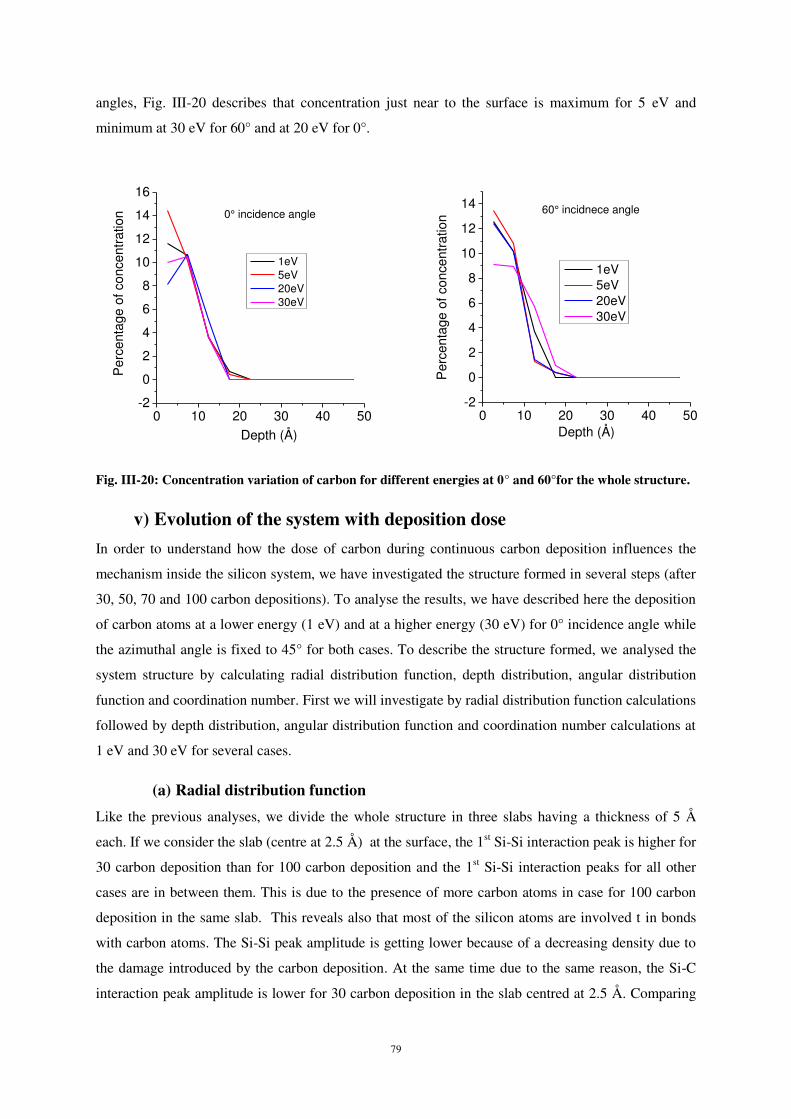
79
angles, Fig. III-20 describes that concentration just near to the surface is maximum for 5 eV and
minimum at 30 eV for 60° and at 20 eV for 0°.
Fig. III-20: Concentration variation of carbon for different energies at 0° and 60°for the whole structure.
v) Evolution of the system with deposition dose
In order to understand how the dose of carbon during continuous carbon deposition influences the
mechanism inside the silicon system, we have investigated the structure formed in several steps (after
30, 50, 70 and 100 carbon depositions). To analyse the results, we have described here the deposition
of carbon atoms at a lower energy (1 eV) and at a higher energy (30 eV) for 0° incidence angle while
the azimuthal angle is fixed to 45° for both cases. To describe the structure formed, we analysed the
system structure by calculating radial distribution function, depth distribution, angular distribution
function and coordination number. First we will investigate by radial distribution function calculations
followed by depth distribution, angular distribution function and coordination number calculations at
1 eV and 30 eV for several cases.
(a) Radial distribution function
Like the previous analyses, we divide the whole structure in three slabs having a thickness of 5 Å
each. If we consider the slab (centre at 2.5 Å) at the surface, the 1st Si-Si interaction peak is higher for
30 carbon deposition than for 100 carbon deposition and the 1st Si-Si interaction peaks for all other
cases are in between them. This is due to the presence of more carbon atoms in case for 100 carbon
deposition in the same slab. This reveals also that most of the silicon atoms are involved t in bonds
with carbon atoms. The Si-Si peak amplitude is getting lower because of a decreasing density due to
the damage introduced by the carbon deposition. At the same time due to the same reason, the Si-C
interaction peak amplitude is lower for 30 carbon deposition in the slab centred at 2.5 Å. Comparing
0 10 20 30 40 50-2
0
2
4
6
8
10
12
14 60° incidnece angle
Per
cent
age
of c
once
ntra
tion
Depth (Å)
1eV 5eV 20eV 30eV
0 10 20 30 40 50-2
0
2
4
6
8
10
12
14
16
0° incidence angle
Per
cent
age
of c
once
ntra
tion
Depth (Å)
1eV 5eV 20eV 30eV
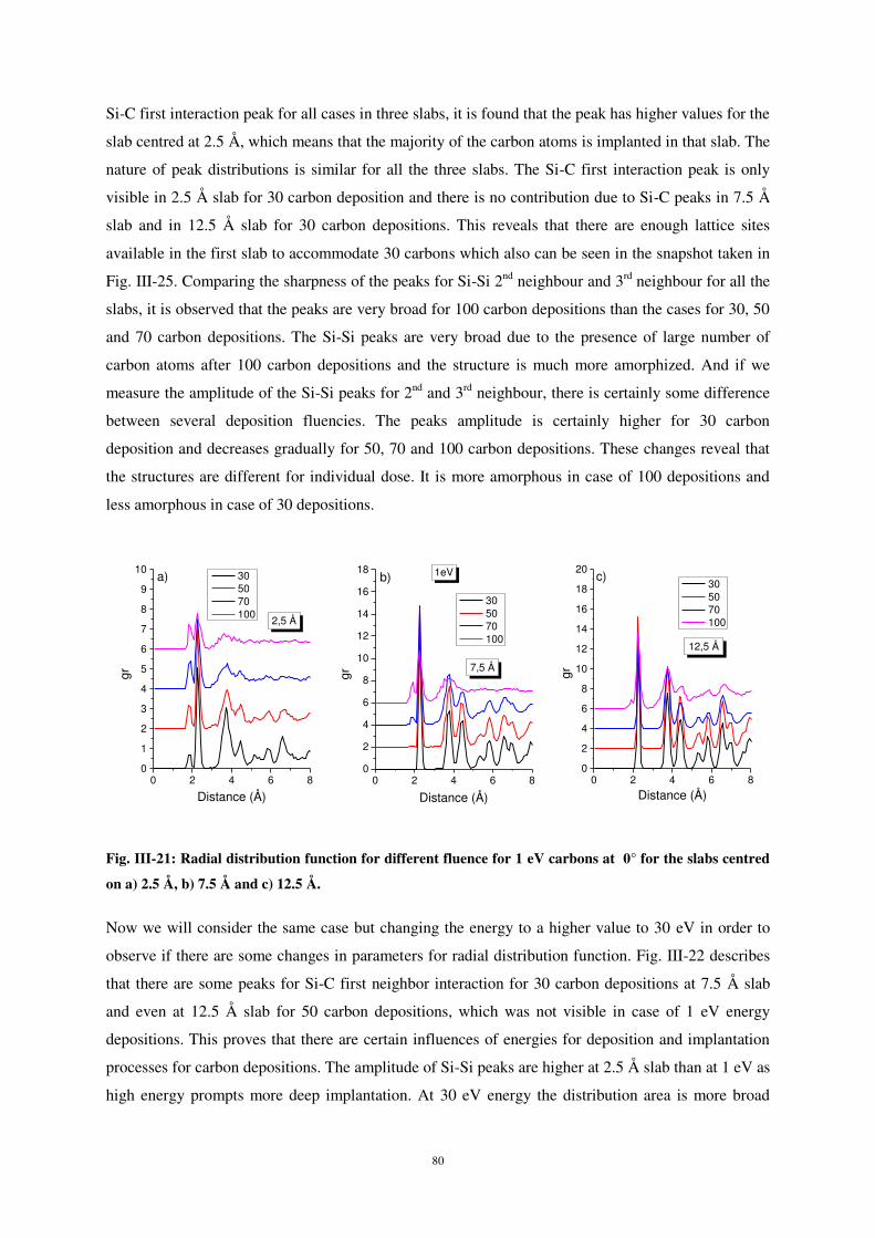
80
Si-C first interaction peak for all cases in three slabs, it is found that the peak has higher values for the
slab centred at 2.5 Å, which means that the majority of the carbon atoms is implanted in that slab. The
nature of peak distributions is similar for all the three slabs. The Si-C first interaction peak is only
visible in 2.5 Å slab for 30 carbon deposition and there is no contribution due to Si-C peaks in 7.5 Å
slab and in 12.5 Å slab for 30 carbon depositions. This reveals that there are enough lattice sites
available in the first slab to accommodate 30 carbons which also can be seen in the snapshot taken in
Fig. III-25. Comparing the sharpness of the peaks for Si-Si 2nd neighbour and 3rd neighbour for all the
slabs, it is observed that the peaks are very broad for 100 carbon depositions than the cases for 30, 50
and 70 carbon depositions. The Si-Si peaks are very broad due to the presence of large number of
carbon atoms after 100 carbon depositions and the structure is much more amorphized. And if we
measure the amplitude of the Si-Si peaks for 2nd and 3rd neighbour, there is certainly some difference
between several deposition fluencies. The peaks amplitude is certainly higher for 30 carbon
deposition and decreases gradually for 50, 70 and 100 carbon depositions. These changes reveal that
the structures are different for individual dose. It is more amorphous in case of 100 depositions and
less amorphous in case of 30 depositions.
Fig. III-21: Radial distribution function for different fluence for 1 eV carbons at 0° for the slabs centred
on a) 2.5 Å, b) 7.5 Å and c) 12.5 Å.
Now we will consider the same case but changing the energy to a higher value to 30 eV in order to
observe if there are some changes in parameters for radial distribution function. Fig. III-22 describes
that there are some peaks for Si-C first neighbor interaction for 30 carbon depositions at 7.5 Å slab
and even at 12.5 Å slab for 50 carbon depositions, which was not visible in case of 1 eV energy
depositions. This proves that there are certain influences of energies for deposition and implantation
processes for carbon depositions. The amplitude of Si-Si peaks are higher at 2.5 Å slab than at 1 eV as
high energy prompts more deep implantation. At 30 eV energy the distribution area is more broad
0 2 4 6 80
2
4
6
8
10
12
14
16
18
20
12,5 Å
c)gr
Distance (Å)
30 50 70 100
0 2 4 6 80
2
4
6
8
10
12
14
16
18 1eV
7,5 Å
b)
gr
Distance (Å)
30 50 70 100
0 2 4 6 80
1
2
3
4
5
6
7
8
9
10
2,5 Å
a)
gr
Distance (Å)
30 50 70 100
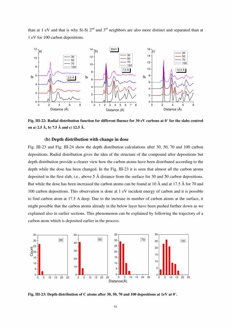
81
than at 1 eV and that is why Si-Si 2nd and 3rd neighbors are also more distinct and separated than at
1 eV for 100 carbon depositions.
Fig. III-22: Radial distribution function for different fluence for 30 eV carbons at 0° for the slabs centred
on a) 2.5 Å, b) 7.5 Å and c) 12.5 Å.
(b) Depth distribution with change in dose
Fig. III-23 and Fig. III-24 show the depth distribution calculations after 30, 50, 70 and 100 carbon
depositions. Radial distribution gives the idea of the structure of the compound after depositions but
depth distribution provide a clearer view how the carbon atoms have been distributed according to the
depth while the dose has been changed. In the Fig. III-23 it is seen that almost all the carbon atoms
deposited in the first slab, i.e., above 5 Å distance from the surface for 30 and 50 carbon depositions.
But while the dose has been increased the carbon atoms can be found at 10 Å and at 17.5 Å for 70 and
100 carbon depositions. This observation is done at 1 eV incident energy of carbon and it is possible
to find carbon atom at 17.5 A deep. Due to the increase in number of carbon atoms at the surface, it
might possible that the carbon atoms already in the below layer have been pushed further down as we
explained also in earlier sections. This phenomenon can be explained by following the trajectory of a
carbon atom which is deposited earlier in the process.
Fig. III-23: Depth distribution of C atoms after 30, 50, 70 and 100 depositions at 1eV at 0°.
0 2 4 6 80
2
4
6
8
10
12
14
16c)
12,5 Å
gr
Distance (Å)
30 50 70 100
0 1 2 3 4 5 6 7 80
2
4
6
8
10
12
14 30eVb)
7,5 Å
gr
Distance (Å)
30 50 70 100
0 2 4 6 80
2
4
6
8
10
12a)
2,5 Ågr
Distance (Å)
30 50 70 100
0 5 10 15 20 250
5
10
15
20
25
30
100
0 5 10 15 20 250
5
10
15
20
25
30
35
Distance(Å)
70
0 5 10 15 20 250
10
20
30
40
50
50
0 5 10 15 20 250
5
10
15
20
25
30
35
Cou
nt
30
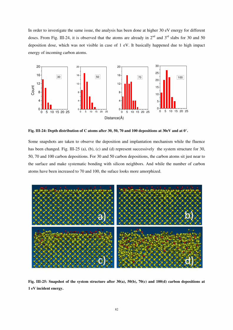
82
In order to investigate the same issue, the analysis has been done at higher 30 eV energy for different
doses. From Fig. III-24, it is observed that the atoms are already in 2nd and 3rd slabs for 30 and 50
deposition dose, which was not visible in case of 1 eV. It basically happened due to high impact
energy of incoming carbon atoms.
Fig. III-24: Depth distribution of C atoms after 30, 50, 70 and 100 depositions at 30eV and at 0°.
Some snapshots are taken to observe the deposition and implantation mechanism while the fluence
has been changed. Fig. III-25 (a), (b), (c) and (d) represent successively the system structure for 30,
50, 70 and 100 carbon depositions. For 30 and 50 carbon depositions, the carbon atoms sit just near to
the surface and make systematic bonding with silicon neighbors. And while the number of carbon
atoms have been increased to 70 and 100, the suface looks more amorphized.
Fig. III-25: Snapshot of the system structure after 30(a), 50(b), 70(c) and 100(d) carbon depositions at
1 eV incident energy.
0 5 10 15 20 250
5
10
15
20
25
30
100
0 5 10 15 20 250
4
8
12
16
20
Distance(Å)
70
0 5 10 15 20 250
4
8
12
16
20
50
0 5 10 15 20 250
4
8
12
16
20
Cou
nt
30
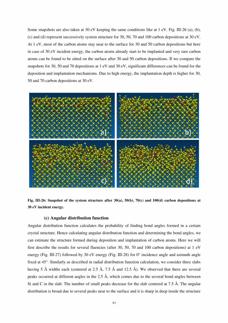
83
Some snapshots are also taken at 30 eV keeping the same conditions like at 1 eV. Fig. III-26 (a), (b),
(c) and (d) represent successively system structure for 30, 50, 70 and 100 carbon depositions at 30 eV.
At 1 eV, most of the carbon atoms stay near to the surface for 30 and 50 carbon depositions but here
in case of 30 eV incident energy, the carbon atoms already start to be implanted and very rare carbon
atoms can be found to be sitted on the surface after 30 and 50 carbon depositions. If we compare the
snapshots for 30, 50 and 70 depositions at 1 eV and 30 eV, significant differences can be found for the
deposition and implantation mechanisms. Due to high energy, the implantation depth is higher for 30,
50 and 70 carbon depositions at 30 eV.
Fig. III-26: Snapshot of the system structure after 30(a), 50(b), 70(c) and 100(d) carbon depositions at
30 eV incident energy.
(c) Angular distribution function
Angular distribution function calculates the probability of finding bond angles formed in a certain
crystal structure. Hence calculating angular distribution function and determining the bond angles, we
can estimate the structure formed during deposition and implantation of carbon atoms. Here we will
first describe the results for several fluencies (after 30, 50, 70 and 100 carbon depositions) at 1 eV
energy (Fig. III-27) followed by 30 eV energy (Fig. III-28) for 0° incidence angle and azimuth angle
fixed at 45°. Similarly as described in radial distribution function calculation, we consider three slabs
having 5 Å widths each (centered at 2.5 Å, 7.5 Å and 12.5 Å). We observed that there are several
peaks occurred at different angles in the 2.5 Å, which comes due to the several bond angles between
Si and C in the slab. The number of small peaks decrease for the slab centered at 7.5 Å. The angular
distribution is broad due to several peaks near to the surface and it is sharp in deep inside the structure
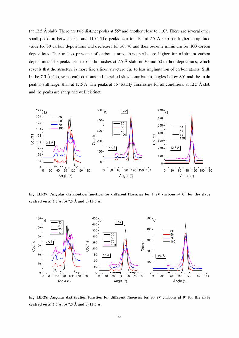
84
(at 12.5 Å slab). There are two distinct peaks at 55° and another close to 110°. There are several other
small peaks in between 55° and 110°. The peaks near to 110° at 2.5 Å slab has higher amplitude
value for 30 carbon depositions and decreases for 50, 70 and then become minimum for 100 carbon
depositions. Due to less presence of carbon atoms, these peaks are higher for minimum carbon
depositions. The peaks near to 55° diminishes at 7.5 Å slab for 30 and 50 carbon depositions, which
reveals that the structure is more like silicon structure due to less implantation of carbon atoms. Still,
in the 7.5 Å slab, some carbon atoms in interstitial sites contribute to angles below 80° and the main
peak is still larger than at 12.5 Å. The peaks at 55° totally diminishes for all conditions at 12.5 Å slab
and the peaks are sharp and well distinct.
Fig. III-27: Angular distribution function for different fluencies for 1 eV carbons at 0° for the slabs
centred on a) 2.5 Å, b) 7.5 Å and c) 12.5 Å.
Fig. III-28: Angular distribution function for different fluencies for 30 eV carbons at 0° for the slabs
centred on a) 2.5 Å, b) 7.5 Å and c) 12.5 Å.
0 30 60 90 120 150 180
0
100
200
300
400
500
600
700c)
12.5 Å
Cou
nts
Angle (°)
30 50 70 100
0 30 60 90 120 150 180
0
100
200
300
400
500 1eVb)
7.5 Å
Cou
nts
Angle (°)
30 50 70 100
0 30 60 90 120 150 1800
25
50
75
100
125
150
175
200
225a)
2.5 ÅCou
nts
Angle (°)
30 50 70 100
0 30 60 90 120 150 1800
100
200
300
400
500c)
12.5 Å
Cou
nts
Angle (°)
30 50 70 100
0 30 60 90 120 150 1800
50
100
150
200
250
300
350
400
45030eVb)
7.5 Å
Cou
nts
Angle (°)
30 50 70 100
0 30 60 90 120 150 1800
30
60
90
120
150
180a)
2.5 Å
Cou
nts
Angle (°)
30 50 70 100
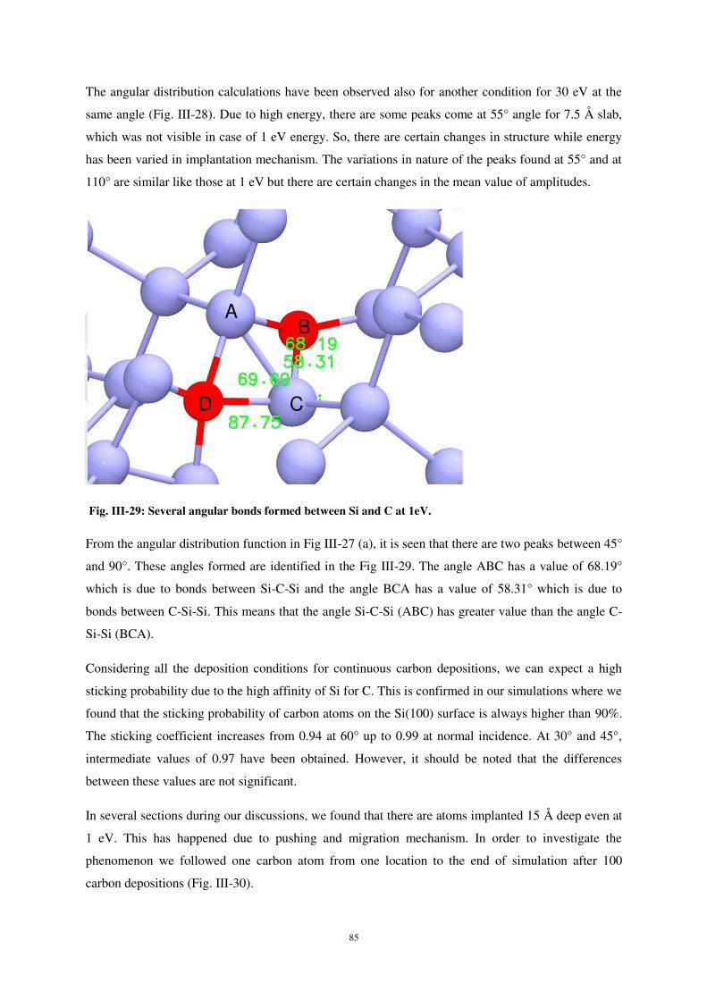
85
The angular distribution calculations have been observed also for another condition for 30 eV at the
same angle (Fig. III-28). Due to high energy, there are some peaks come at 55° angle for 7.5 Å slab,
which was not visible in case of 1 eV energy. So, there are certain changes in structure while energy
has been varied in implantation mechanism. The variations in nature of the peaks found at 55° and at
110° are similar like those at 1 eV but there are certain changes in the mean value of amplitudes.
Fig. III-29: Several angular bonds formed between Si and C at 1eV.
From the angular distribution function in Fig III-27 (a), it is seen that there are two peaks between 45°
and 90°. These angles formed are identified in the Fig III-29. The angle ABC has a value of 68.19°
which is due to bonds between Si-C-Si and the angle BCA has a value of 58.31° which is due to
bonds between C-Si-Si. This means that the angle Si-C-Si (ABC) has greater value than the angle C-
Si-Si (BCA).
Considering all the deposition conditions for continuous carbon depositions, we can expect a high
sticking probability due to the high affinity of Si for C. This is confirmed in our simulations where we
found that the sticking probability of carbon atoms on the Si(100) surface is always higher than 90%.
The sticking coefficient increases from 0.94 at 60° up to 0.99 at normal incidence. At 30° and 45°,
intermediate values of 0.97 have been obtained. However, it should be noted that the differences
between these values are not significant.
In several sections during our discussions, we found that there are atoms implanted 15 Å deep even at
1 eV. This has happened due to pushing and migration mechanism. In order to investigate the
phenomenon we followed one carbon atom from one location to the end of simulation after 100
carbon depositions (Fig. III-30).
AB
CD
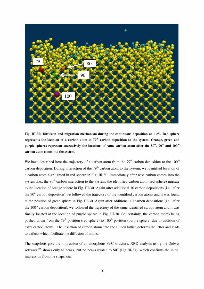
86
Fig. III-30: Diffusion and migration mechanism during the continuous deposition at 1 eV. Red sphere
represents the location of a carbon atom at 79th carbon deposition to the system. Orange, green and
purple spheres represent successively the locations of same carbon atom after the 80th, 90th and 100th
carbon atom come into the system.
We have described here the trajectory of a carbon atom from the 79th carbon deposition to the 100th
carbon deposition. During interaction of the 79th carbon atom to the system, we identified location of
a carbon atom highlighted in red sphere in Fig. III-30. Immediately after next carbon comes into the
system ,i.e., the 80th carbon interaction to the system, the identified carbon atom (red sphere) migrate
to the location of orange sphere in Fig. III-30. Again after additional 10 carbon depositions (i.e., after
the 90th carbon deposition) we followed the trajectory of the identified carbon atoms and it was found
at the position of green sphere in Fig. III-30. Again after additional 10 carbon depositions (i.e., after
the 100th carbon deposition), we followed the trajectory of the same identified carbon atom and it was
finally located at the location of purple sphere in Fig. III-30. So, certainly, the carbon atoms being
pushed down from the 79th position (red sphere) to 100th position (purple sphere) due to addition of
extra carbon atoms. The insertion of carbon atoms into the silicon lattice deforms the latter and leads
to defects which facilitate the diffusion of atoms.
The snapshots give the impression of an amorphous Si-C structure. XRD analysis using the Debyer
software136 shows only Si peaks, but no peaks related to SiC (Fig III-31), which confirms the initial
impression from the snapshots.
79 80
90
100
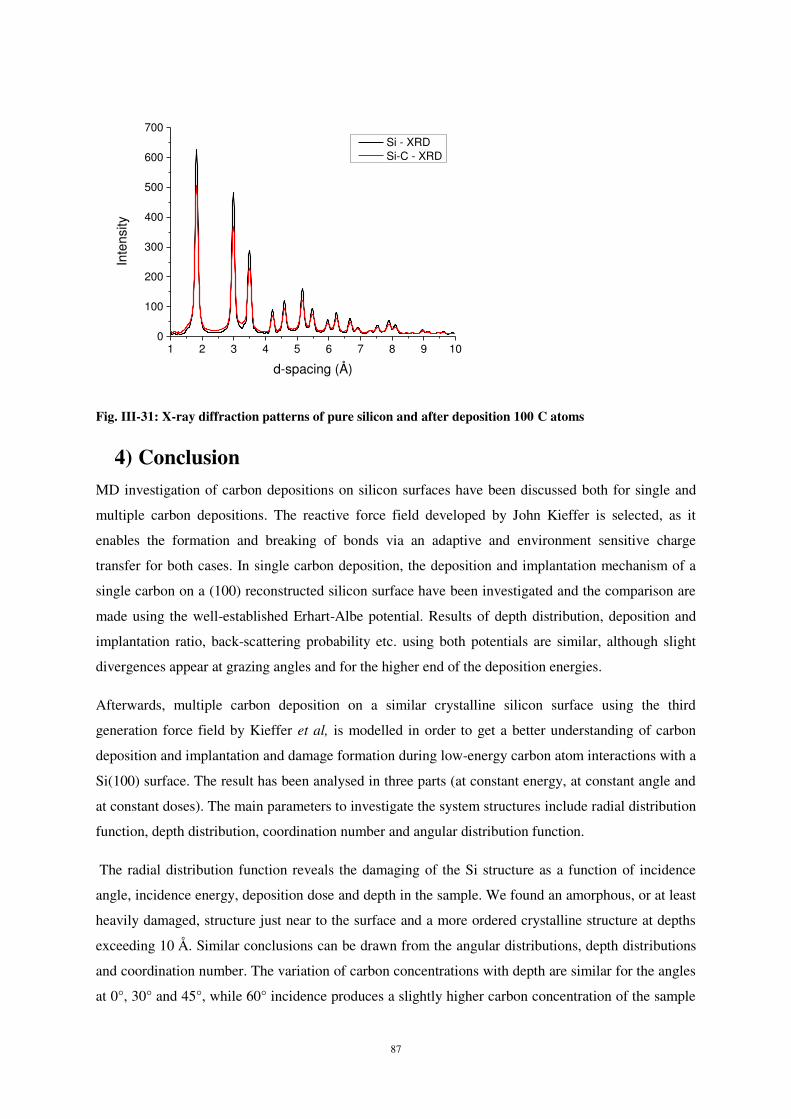
87
Fig. III-31: X-ray diffraction patterns of pure silicon and after deposition 100 C atoms
4) Conclusion MD investigation of carbon depositions on silicon surfaces have been discussed both for single and
multiple carbon depositions. The reactive force field developed by John Kieffer is selected, as it
enables the formation and breaking of bonds via an adaptive and environment sensitive charge
transfer for both cases. In single carbon deposition, the deposition and implantation mechanism of a
single carbon on a (100) reconstructed silicon surface have been investigated and the comparison are
made using the well-established Erhart-Albe potential. Results of depth distribution, deposition and
implantation ratio, back-scattering probability etc. using both potentials are similar, although slight
divergences appear at grazing angles and for the higher end of the deposition energies.
Afterwards, multiple carbon deposition on a similar crystalline silicon surface using the third
generation force field by Kieffer et al, is modelled in order to get a better understanding of carbon
deposition and implantation and damage formation during low-energy carbon atom interactions with a
Si(100) surface. The result has been analysed in three parts (at constant energy, at constant angle and
at constant doses). The main parameters to investigate the system structures include radial distribution
function, depth distribution, coordination number and angular distribution function.
The radial distribution function reveals the damaging of the Si structure as a function of incidence
angle, incidence energy, deposition dose and depth in the sample. We found an amorphous, or at least
heavily damaged, structure just near to the surface and a more ordered crystalline structure at depths
exceeding 10 Å. Similar conclusions can be drawn from the angular distributions, depth distributions
and coordination number. The variation of carbon concentrations with depth are similar for the angles
at 0°, 30° and 45°, while 60° incidence produces a slightly higher carbon concentration of the sample
1 2 3 4 5 6 7 8 9 100
100
200
300
400
500
600
700In
tens
ity
d-spacing (Å)
Si - XRD Si-C - XRD

88
surface at constant incident energy 5eV. The results at different doses show how the deposition
mechanism changes while the fluencies have been varied. Some snapshots also confirm the
mechanisms. Finally, the results of radial distribution functions, depth distributions, coordination
number and angular distributions give several aspects of deposition and implantation mechanism for
continuous carbon depositions. The results might give some important insight in SiC formation and
interface formation as the properties of SiC devices and films largely depend on defects.
Importantly, even in the sub monolayer range the carbon deposition strongly modifies the top layer of
silicon surface, which gives important insights into the deposition process and which should be
accounted for in future studies.
89
Ti deposition on Si
“Sticking coefficient of titanium on silicon
surfaces has been investigated by storing matter
and SIMS technique as well as by numerical
simulations.”

90
91
Chapitre 4.
Titanium (Ti) deposition on Silicon (Si)
1) Introduction: This chapter deals with fundamental aspects of depositing titanium (Ti) on silicon (Si) in the sub-
monolayer range in order to understand where and under which conditions the atoms stick on the
substrate. Hence, the sub-monolayer film deposition of Ti on Si(100) is discussed for various fluences
by changing the primary current and the deposition time.
The choice of key parameters for the deposition conditions in storing matter chamber have been
chosen for sub-monolayer films. The parameters for the analyses by dynamic SIMS also were chosen
for very dilute deposits in order to obtain sufficiently low sputter rates. The sputtered particles
consisting of charged and neutral atoms or particles are sputtered by Ar+ ions from the sample and
collected on the substrate surface with a certain angular distribution depending upon the positioning
of collector, target and ion beam. The ejected particles are thus non-uniformly spread over a certain
area of the collector (Si) to form the deposit. In order to investigate the distribution of the atoms in the
collector surface, several dynamic SIMS analyses were done across the deposit along vertical and
horizontal directions to find the centre of the deposit and record its shapes. A maximum intensity is
found near to the edge of the collector. In order to collect a maximum of the sputtered particles, the
substrate Si collector should be placed closer to the FLIG (Floating Low Energy Ion Gun). In that
case, special care should be taken that some part of the substrate should not cut the incident ion beam.
The shape of all the deposits is same, which reveals that the angular distribution is similar for all
deposits.
In this chapter along with experimental results, we will describe some molecular dynamics and DFT
results for titanium, which were previously obtained by a postdoc researcher in our group 123. Later
some comparisons will be made between the simulation and experimental results. The parameter by
which both methods can be compared is the sticking coefficient.
2) Experimental setup and conditions
i) Collector (Si) and Target (Ti) preparation process
Silicon wafers of 1 inch diameter have been chosen as collector material. In order to remove surface
contaminations, the Si wafer is cleaned successively with deionised water, acetone and ethanol in an
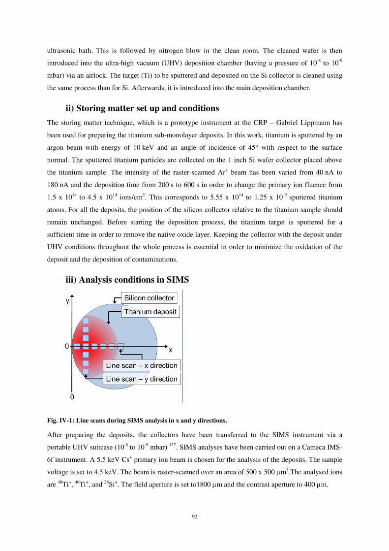
92
ultrasonic bath. This is followed by nitrogen blow in the clean room. The cleaned wafer is then
introduced into the ultra-high vacuum (UHV) deposition chamber (having a pressure of 10-8 to 10-9
mbar) via an airlock. The target (Ti) to be sputtered and deposited on the Si collector is cleaned using
the same process than for Si. Afterwards, it is introduced into the main deposition chamber.
ii) Storing matter set up and conditions
The storing matter technique, which is a prototype instrument at the CRP – Gabriel Lippmann has
been used for preparing the titanium sub-monolayer deposits. In this work, titanium is sputtered by an
argon beam with energy of 10 keV and an angle of incidence of 45° with respect to the surface
normal. The sputtered titanium particles are collected on the 1 inch Si wafer collector placed above
the titanium sample. The intensity of the raster-scanned Ar+ beam has been varied from 40 nA to
180 nA and the deposition time from 200 s to 600 s in order to change the primary ion fluence from
1.5 x 10¹⁴ to 4.5 x 10¹⁴ ions/cm2. This corresponds to 5.55 x 10¹⁴ to 1.25 x 10¹⁵ sputtered titanium
atoms. For all the deposits, the position of the silicon collector relative to the titanium sample should
remain unchanged. Before starting the deposition process, the titanium target is sputtered for a
sufficient time in order to remove the native oxide layer. Keeping the collector with the deposit under
UHV conditions throughout the whole process is essential in order to minimize the oxidation of the
deposit and the deposition of contaminations.
iii) Analysis conditions in SIMS
Fig. IV-1: Line scans during SIMS analysis in x and y directions.
After preparing the deposits, the collectors have been transferred to the SIMS instrument via a
portable UHV suitcase (10-8 to 10-9 mbar) 137. SIMS analyses have been carried out on a Cameca IMS-
6f instrument. A 5.5 keV Cs+ primary ion beam is chosen for the analysis of the deposits. The sample
voltage is set to 4.5 keV. The beam is raster-scanned over an area of 500 x 500 µm2.The analysed ions
are 48Ti+, 46Ti+, and 28Si+. The field aperture is set to1800 µm and the contrast aperture to 400 µm.
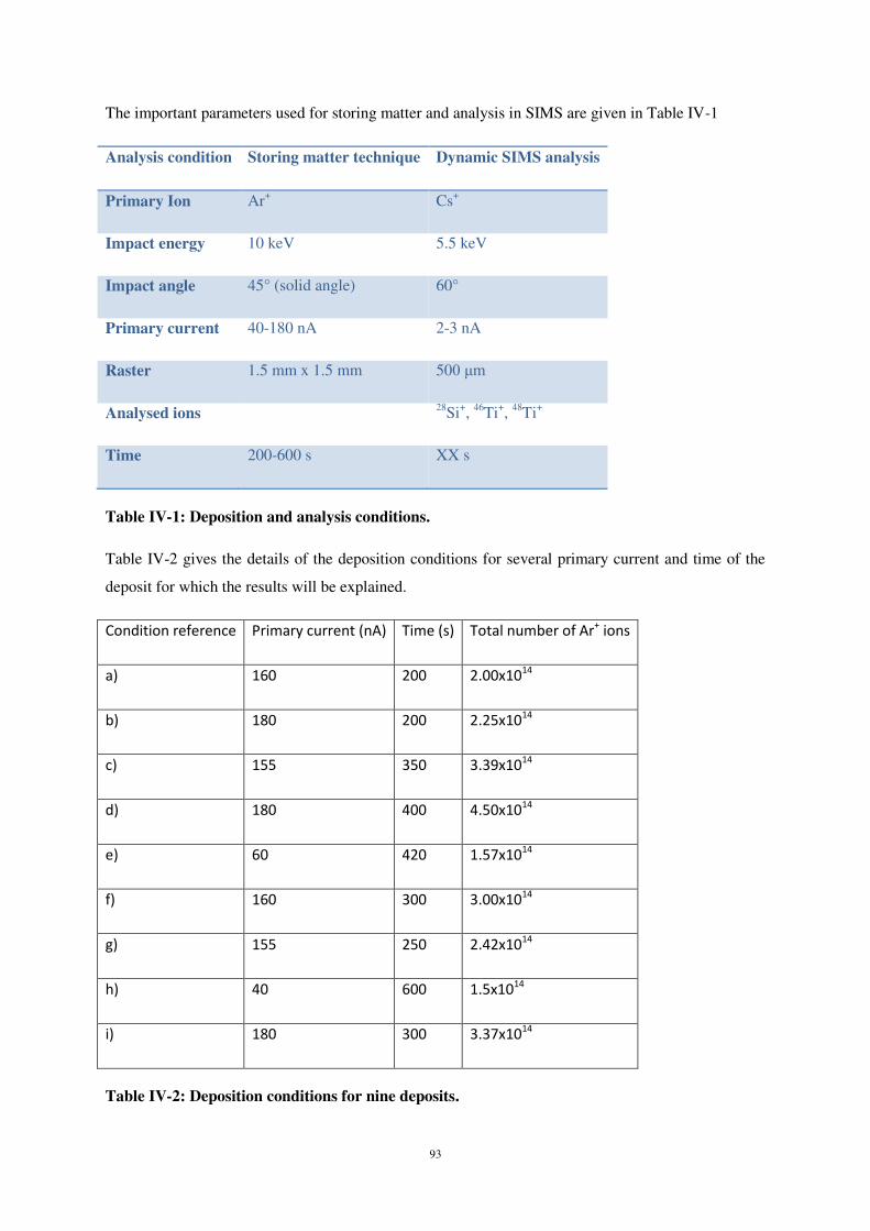
93
The important parameters used for storing matter and analysis in SIMS are given in Table IV-1
Analysis condition Storing matter technique Dynamic SIMS analysis
Primary Ion Ar+ Cs+
Impact energy 10 keV 5.5 keV
Impact angle 45° (solid angle) 60°
Primary current 40-180 nA 2-3 nA
Raster 1.5 mm x 1.5 mm 500 m
Analysed ions 28Si+, 46Ti+, 48Ti+
Time 200-600 s XX s
Table IV-1: Deposition and analysis conditions.
Table IV-2 gives the details of the deposition conditions for several primary current and time of the
deposit for which the results will be explained.
Condition reference Primary current (nA) Time (s) Total number of Ar+ ions
a) 160 200 2.00x10¹⁴
b) 180 200 2.25x10¹⁴
c) 155 350 3.39x10¹⁴
d) 180 400 4.50x10¹⁴
e) 60 420 1.57x10¹⁴
f) 160 300 3.00x10¹⁴
g) 155 250 2.42x10¹⁴
h) 40 600 1.5x10¹⁴
i) 180 300 3.37x10¹⁴
Table IV-2: Deposition conditions for nine deposits.
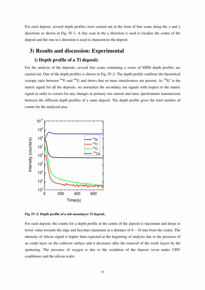
94
For each deposit, several depth profiles were carried out in the form of line scans along the x and y
directions as shown in Fig. IV-1. A line scan in the y direction is used to localize the centre of the
deposit and the one in x direction is used to characterize the deposit.
3) Results and discussion: Experimental
i) Depth profile of a Ti deposit:
For the analysis of the deposits, several line scans containing a series of SIMS depth profiles are
carried out. One of the depth profiles is shown in Fig. IV-2. The depth profile confirms the theoretical
isotopic ratio between 46Ti and 48Ti and shows that no mass interferences are present. As 28Si+ is the
matrix signal for all the deposits, we normalize the secondary ion signals with respect to the matrix
signal in order to correct for any changes in primary ion current and mass spectrometer transmission
between the different depth profiles of a same deposit. The depth profile gives the total number of
counts for the analysed area.
Fig. IV-2: Depth profile of a sub-monolayer Ti deposit.
For each deposit, the counts for a depth profile at the centre of the deposit is maximum and drops to
lower value towards the edge and becomes minimum at a distance of 8 – 10 mm from the centre. The
intensity of silicon signal is higher than expected at the beginning of analysis due to the presence of
an oxide layer on the collector surface and it decreases after the removal of the oxide layers by the
sputtering. The presence of oxygen is due to the oxidation of the deposit (even under UHV
conditions) and the silicon wafer.
0 200 400 600102
103
104
105
106
107
108
109
1010
Inte
nsity
(co
unts
/s)
Time(s)
28Si 46Ti 48Ti 133Cs
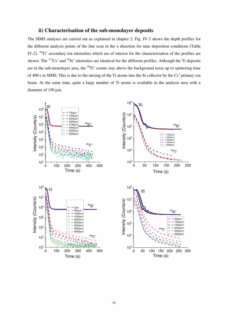
95
ii) Characterisation of the sub-monolayer deposits
The SIMS analyses are carried out as explained in chapter 2. Fig. IV-3 shows the depth profiles for
the different analysis points of the line scan in the x direction for nine deposition conditions (Table
IV-2). 48Ti+ secondary ion intensities which are of interest for the characterisation of the profiles are
shown. The 133Cs+ and 28Si+ intensities are identical for the different profiles. Although the Ti deposits
are in the sub-monolayer area, the 48Ti+ counts stay above the background noise up to sputtering time
of 400 s in SIMS. This is due to the mixing of the Ti atoms into the Si collector by the Cs+ primary ion
beam. At the same time, quite a large number of Ti atoms is available in the analysis area with a
diameter of 150 µm.
0 50 100 150 200 250 300103
104
105
106
107
108
28Si+
48Ti+
d)
Inte
nsity
(C
ount
s/s)
Time (s)
500µm 1000µm 1500µm 2000µm 2500µm 3000µm
0 100 200 300 400 500102
103
104
105
106
107
108
28Si+
48Ti+
c)
Inte
nsity
(C
ount
s/s)
Time (s)
0µm 500µm 1000µm 1500µm 2000µm 2500µm 3000µm 3500µm 4000µm
0 50 100 150 200 250103
104
105
106
107
108
28Si+
48Ti+
Inte
nsity
(C
ount
s/s)
b)
Time (s)
1000µm 2000µm 3000µm 4000µm 5000µm
0 100 200 300 400 500101
102
103
104
105
106
107
108
28Si+
48Ti+
a)
Inte
nsity
(C
ount
s/s)
Time (s)
750µm 1500µm 2250µm 3000µm 3750µm 4500µm 5250µm 6000µm
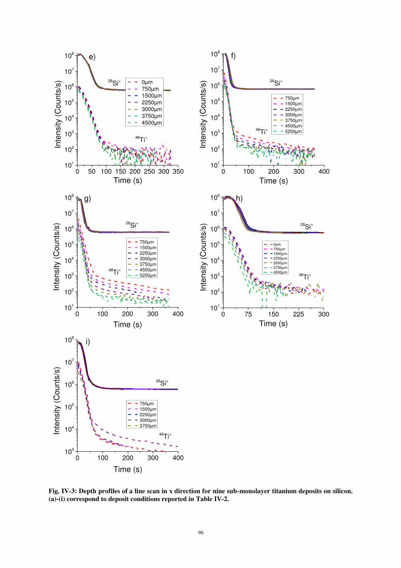
96
Fig. IV-3: Depth profiles of a line scan in x direction for nine sub-monolayer titanium deposits on silicon. (a)-(i) correspond to deposit conditions reported in Table IV-2.
0 50 100 150 200 250 300 350101
102
103
104
105
106
107
108
28Si+
e)
48Ti+
Inte
nsity
(C
ount
s/s)
Time (s)
0µm 750µm 1500µm 2250µm 3000µm 3750µm 4500µm
0 100 200 300 400103
104
105
106
107
108
28Si+
48Ti+
i)
Inte
nsity
(C
ount
s/s)
Time (s)
750µm 1500µm 2250µm 3000µm 3750µm
0 75 150 225 300101
102
103
104
105
106
107
108
28Si+
48Ti+
h) In
tens
ity (
Cou
nts/
s)
Time (s)
0µm 750µm 1500µm 2250µm 3000µm 3750µm 4500µm
0 100 200 300 400101
102
103
104
105
106
107
108
28Si+
48Ti+
g)
Inte
nsity
(C
ount
s/s)
Time (s)
750µm 1500µm 2250µm 3000µm 3750µm 4500µm 5250µm
0 100 200 300 400101
102
103
104
105
106
107
108
28Si+
48Ti+
f)
Inte
nsity
(C
ount
s/s)
Time (s)
750µm 1500µm 2250µm 3000µm 3750µm 4500µm 5250µm
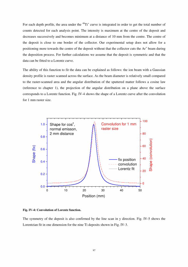
97
For each depth profile, the area under the 48Ti+ curve is integrated in order to get the total number of
counts detected for each analysis point. The intensity is maximum at the centre of the deposit and
decreases successively and becomes minimum at a distance of 10 mm from the centre. The centre of
the deposit is close to one border of the collector. Our experimental setup does not allow for a
positioning more towards the centre of the deposit without that the collector cuts the Ar+ beam during
the deposition process. For further calculations we assume that the deposit is symmetric and that the
data can be fitted to a Lorentz curve.
The ability of this function to fit the data can be explained as follows: the ion beam with a Gaussian
density profile is raster scanned across the surface. As the beam diameter is relatively small compared
to the raster-scanned area and the angular distribution of the sputtered matter follows a cosine law
(reference to chapter 1), the projection of the angular distribution on a plane above the surface
corresponds to a Lorentz function. Fig. IV-4 shows the shape of a Lorentz curve after the convolution
for 1 mm raster size.
0 10 20 30 40 500.0
0.2
0.4
0.6
0.8
1.0
fix position
Sha
pe (
fix)
Position (mm)
Convolution for 1 mmraster size
0
20
40
60
80
100
convolution Lorentz fit S
hape
(co
nvol
utio
n)
Shape for cos2,normal emisson,2 mm distance
Fig. IV-4: Convolution of Lorentz function.
The symmetry of the deposit is also confirmed by the line scan in y direction. Fig. IV-5 shows the
Lorentzian fit in one dimension for the nine Ti deposits shown in Fig. IV-3.
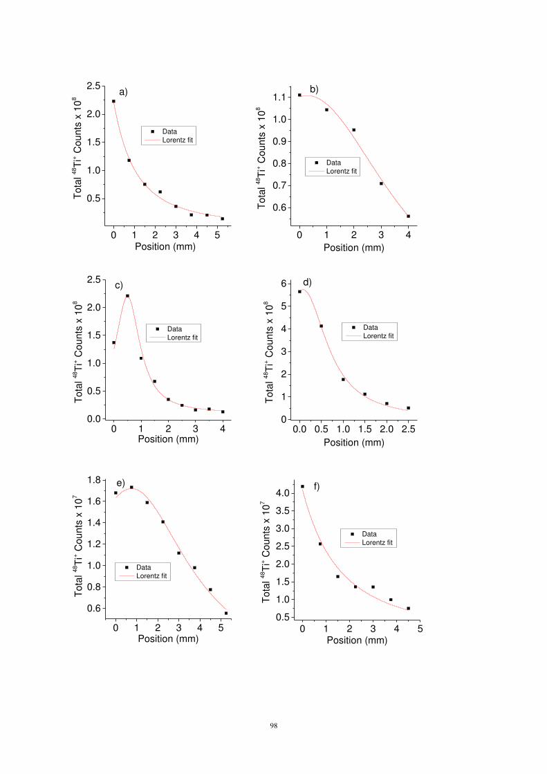
98
0 1 2 3 4
0.6
0.7
0.8
0.9
1.0
1.1b)
Tot
al 48
Ti+ C
ount
s x
108
Position (mm)
Data Lorentz fit
0.0 0.5 1.0 1.5 2.0 2.50
1
2
3
4
5
6 d)T
otal
48T
i+ Cou
nts
x 10
8
Position (mm)
Data Lorentz fit
0 1 2 3 40.0
0.5
1.0
1.5
2.0
2.5 c)
Tot
al 48
Ti+ C
ount
s x
108
Position (mm)
Data Lorentz fit
0 1 2 3 4 5
0.5
1.0
1.5
2.0
2.5a)
Tot
al 48
Ti+ C
ount
s x
108
Position (mm)
Data Lorentz fit
0 1 2 3 4 50.5
1.0
1.5
2.0
2.5
3.0
3.5
4.0f)
Tot
al 48
Ti+ C
ount
s x
107
Position (mm)
Data Lorentz fit
0 1 2 3 4 5
0.6
0.8
1.0
1.2
1.4
1.6
1.8 e)
Tot
al 48
Ti+ C
ount
s x
107
Position (mm)
Data Lorentz fit
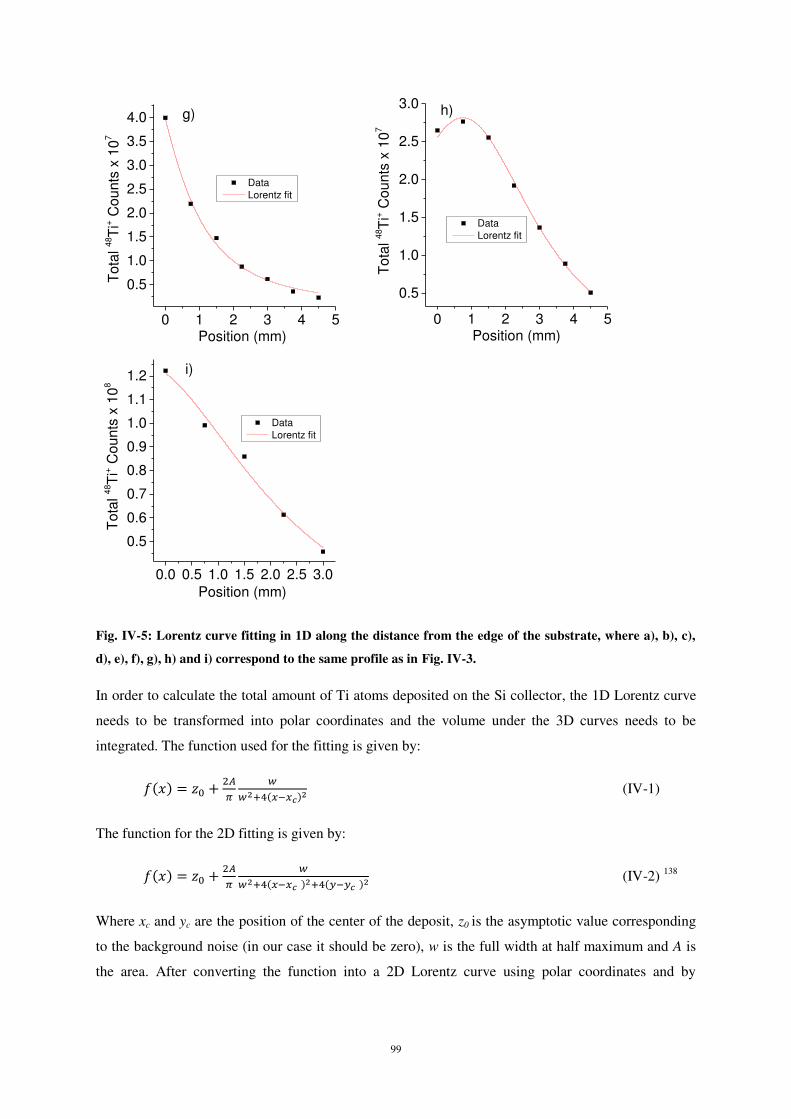
99
Fig. IV-5: Lorentz curve fitting in 1D along the distance from the edge of the substrate, where a), b), c),
d), e), f), g), h) and i) correspond to the same profile as in Fig. IV-3.
In order to calculate the total amount of Ti atoms deposited on the Si collector, the 1D Lorentz curve
needs to be transformed into polar coordinates and the volume under the 3D curves needs to be
integrated. The function used for the fitting is given by:
(IV-1)
The function for the 2D fitting is given by:
(IV-2) 138
Where xc and yc are the position of the center of the deposit, z0 is the asymptotic value corresponding
to the background noise (in our case it should be zero), w is the full width at half maximum and A is
the area. After converting the function into a 2D Lorentz curve using polar coordinates and by
0.0 0.5 1.0 1.5 2.0 2.5 3.0
0.5
0.6
0.7
0.8
0.9
1.0
1.1
1.2 i)
Tot
al 48
Ti+ C
ount
s x
108
Position (mm)
Data Lorentz fit
0 1 2 3 4 5
0.5
1.0
1.5
2.0
2.5
3.0 h)
Tot
al 48
Ti+ C
ount
s x
107
Position (mm)
Data Lorentz fit
0 1 2 3 4 5
0.5
1.0
1.5
2.0
2.5
3.0
3.5
4.0 g)T
otal
48T
i+ Cou
nts
x 10
7
Position (mm)
Data Lorentz fit
100
assuming that the deposit is symmetric, the volume below the curve, i.e. the total number of atoms
detected, is given by:
∫ ∫ (IV-3)
which after integration leads to:
(IV-4)
The values of A and w are obtained from the one dimensional Lorentz fit, while the R value was taken
equal to 10000 m because beyond this value no titanium was detected. The values of A and w of the
fit of all deposits of Fig. IV-5 are given in Table IV-3.
Condition reference Total number of Ar+ ions Area (A) Width (w)
a) 2.00x10¹⁴
7.30x10¹¹
1441.51
b) 2.25x10¹⁴
3.19x10¹¹
7971.45
c) 3.39x10¹⁴
5.50x10¹¹
1666.84
d) 4.50x10¹⁴
1.20x10¹²
1327.60
e) 1.57x10¹⁴
1.76x10¹¹
6524.01
f) 3.00x10¹⁴
1.96x10¹¹
3332.70
g) 2.42x10¹⁴
2.45x10¹¹
2623.08
h) 1.50x10¹⁴
2.82x10¹¹
5241.33
i) 3.37x10¹⁴
1.09x10¹²
6110.18
Table IV-3: Values of A and w for nine deposits.
From the values of A and w, the number of counts can be estimated. However, this number does not
take an ionisation probability less than one and the transmission of the mass spectrometer into
account, i.e. the volume of the deposit is underestimated for the moment.
Knowing the total counts after integrating the Lorentz fit, the total number of actual deposited Ti
particles NTi on the substrate is calculated using the useful yield of Ti in Si:
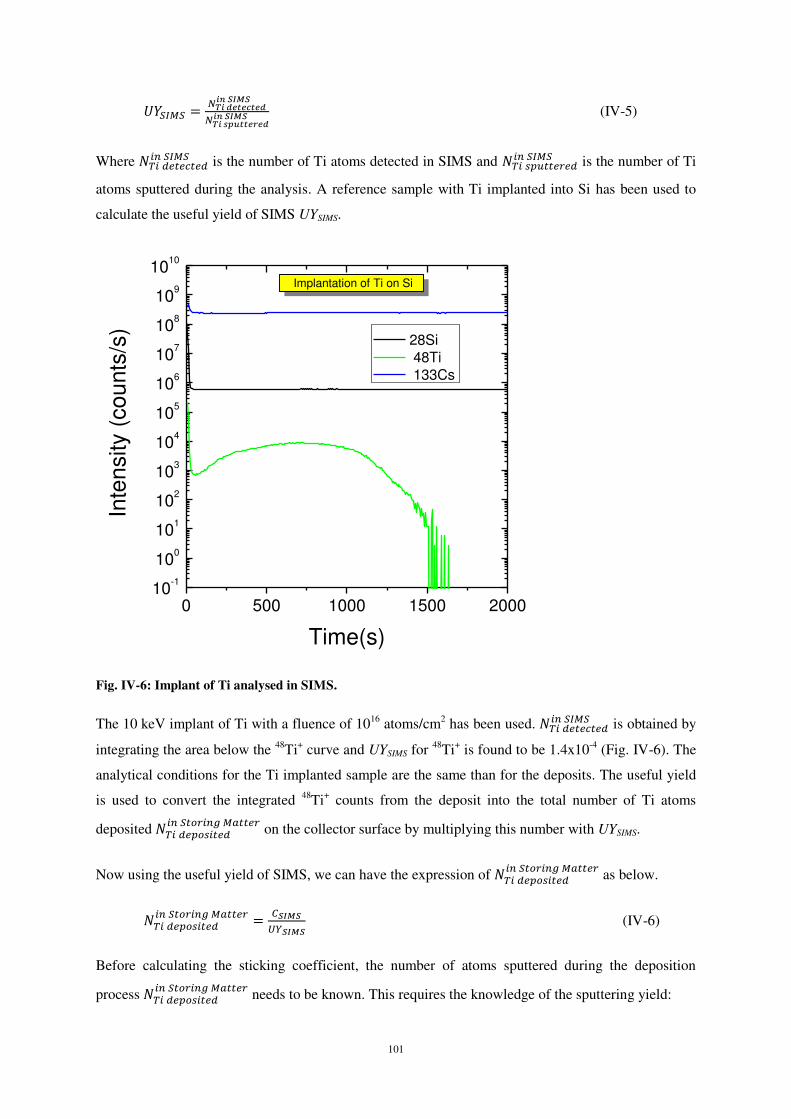
101
(IV-5)
Where is the number of Ti atoms detected in SIMS and is the number of Ti
atoms sputtered during the analysis. A reference sample with Ti implanted into Si has been used to
calculate the useful yield of SIMS UYSIMS.
Fig. IV-6: Implant of Ti analysed in SIMS.
The 10 keV implant of Ti with a fluence of 1016 atoms/cm2 has been used. is obtained by
integrating the area below the 48Ti+ curve and UYSIMS for 48Ti+ is found to be 1.4x10⁻⁴ (Fig. IV-6). The
analytical conditions for the Ti implanted sample are the same than for the deposits. The useful yield
is used to convert the integrated 48Ti+ counts from the deposit into the total number of Ti atoms
deposited on the collector surface by multiplying this number with UYSIMS.
Now using the useful yield of SIMS, we can have the expression of as below.
(IV-6)
Before calculating the sticking coefficient, the number of atoms sputtered during the deposition
process needs to be known. This requires the knowledge of the sputtering yield:
0 500 1000 1500 200010-1
100
101
102
103
104
105
106
107
108
109
1010
Implantation of Ti on Si
Inte
nsity
(co
unts
/s)
Time(s)
28Si 48Ti 133Cs
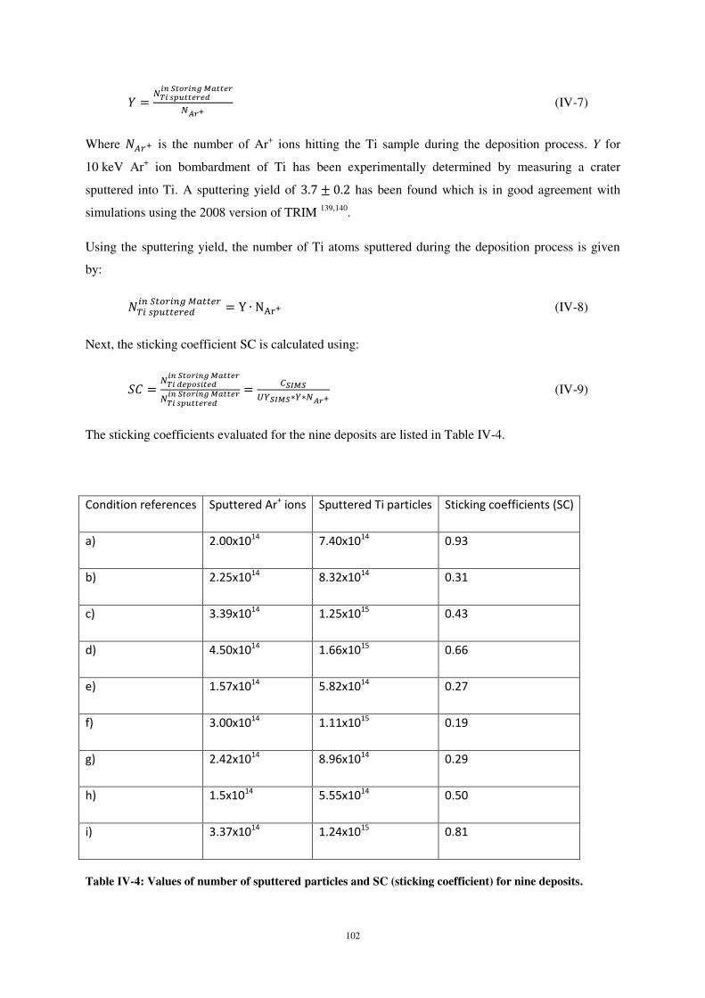
102
(IV-7)
Where is the number of Ar+ ions hitting the Ti sample during the deposition process. Y for
10 keV Ar+ ion bombardment of Ti has been experimentally determined by measuring a crater
sputtered into Ti. A sputtering yield of has been found which is in good agreement with
simulations using the 2008 version of TRIM 139,140.
Using the sputtering yield, the number of Ti atoms sputtered during the deposition process is given
by:
(IV-8)
Next, the sticking coefficient SC is calculated using:
(IV-9)
The sticking coefficients evaluated for the nine deposits are listed in Table IV-4.
Condition references Sputtered Ar+ ions Sputtered Ti particles Sticking coefficients (SC)
a) 2.00x10¹⁴
7.40x10¹⁴
0.93
b) 2.25x10¹⁴
8.32x10¹⁴
0.31
c) 3.39x10¹⁴
1.25x10¹⁵
0.43
d) 4.50x10¹⁴
1.66x10¹⁵
0.66
e) 1.57x10¹⁴
5.82x10¹⁴
0.27
f) 3.00x10¹⁴
1.11x10¹⁵
0.19
g) 2.42x10¹⁴
8.96x10¹⁴
0.29
h) 1.5x10¹⁴
5.55x10¹⁴
0.50
i) 3.37x10¹⁴
1.24x10¹⁵
0.81
Table IV-4: Values of number of sputtered particles and SC (sticking coefficient) for nine deposits.
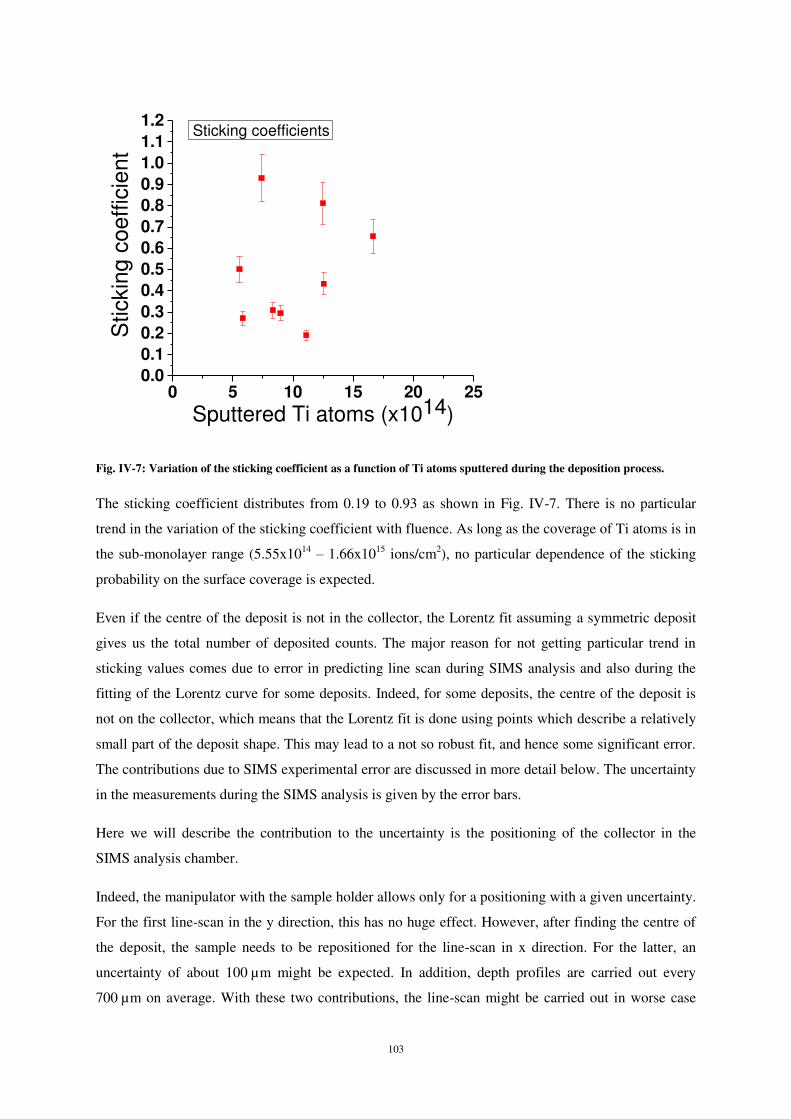
103
Fig. IV-7: Variation of the sticking coefficient as a function of Ti atoms sputtered during the deposition process.
The sticking coefficient distributes from 0.19 to 0.93 as shown in Fig. IV-7. There is no particular
trend in the variation of the sticking coefficient with fluence. As long as the coverage of Ti atoms is in
the sub-monolayer range (5.55x10¹⁴ – 1.66x10¹⁵ ions/cm2), no particular dependence of the sticking
probability on the surface coverage is expected.
Even if the centre of the deposit is not in the collector, the Lorentz fit assuming a symmetric deposit
gives us the total number of deposited counts. The major reason for not getting particular trend in
sticking values comes due to error in predicting line scan during SIMS analysis and also during the
fitting of the Lorentz curve for some deposits. Indeed, for some deposits, the centre of the deposit is
not on the collector, which means that the Lorentz fit is done using points which describe a relatively
small part of the deposit shape. This may lead to a not so robust fit, and hence some significant error.
The contributions due to SIMS experimental error are discussed in more detail below. The uncertainty
in the measurements during the SIMS analysis is given by the error bars.
Here we will describe the contribution to the uncertainty is the positioning of the collector in the
SIMS analysis chamber.
Indeed, the manipulator with the sample holder allows only for a positioning with a given uncertainty.
For the first line-scan in the y direction, this has no huge effect. However, after finding the centre of
the deposit, the sample needs to be repositioned for the line-scan in x direction. For the latter, an
uncertainty of about 100 µm might be expected. In addition, depth profiles are carried out every
700 µm on average. With these two contributions, the line-scan might be carried out in worse case
0 5 10 15 20 250.0
0.1
0.2
0.3
0.4
0.5
0.6
0.7
0.8
0.9
1.0
1.1
1.2Sticking coefficients
Stic
king
coe
ffici
ent
Sputtered Ti atoms (x1014)
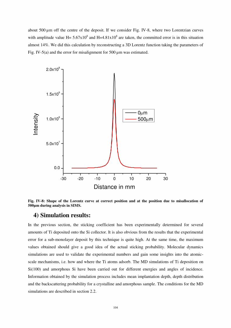
104
about 500 µm off the centre of the deposit. If we consider Fig. IV-8, where two Lorentzian curves
with amplitude value H= 5.67x10⁸ and H=4.81x10⁸ are taken, the committed error is in this situation
almost 14%. We did this calculation by reconstructing a 3D Lorentz function taking the parameters of
Fig. IV-5(a) and the error for misalignment for 500 µm was estimated.
-30 -20 -10 0 10 20 30
0.0
5.0x10⁷
1.0x10⁸
1.5x10⁸
2.0x10⁸
Inte
nsity
Distance in mm
0m 500m
Fig. IV-8: Shape of the Lorentz curve at correct position and at the position due to misallocation of 500µm during analysis in SIMS.
4) Simulation results: In the previous section, the sticking coefficient has been experimentally determined for several
amounts of Ti deposited onto the Si collector. It is also obvious from the results that the experimental
error for a sub-monolayer deposit by this technique is quite high. At the same time, the maximum
values obtained should give a good idea of the actual sticking probability. Molecular dynamics
simulations are used to validate the experimental numbers and gain some insights into the atomic-
scale mechanisms, i.e. how and where the Ti atoms adsorb. The MD simulations of Ti deposition on
Si(100) and amorphous Si have been carried out for different energies and angles of incidence.
Information obtained by the simulation process includes mean implantation depth, depth distribution
and the backscattering probability for a crystalline and amorphous sample. The conditions for the MD
simulations are described in section 2.2.
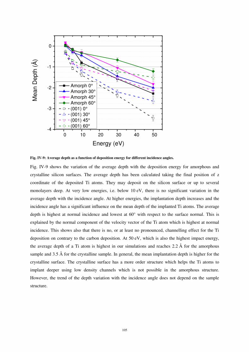
105
Fig. IV-9: Average depth as a function of deposition energy for different incidence angles.
Fig. IV-9 shows the variation of the average depth with the deposition energy for amorphous and
crystalline silicon surfaces. The average depth has been calculated taking the final position of z
coordinate of the deposited Ti atoms. They may deposit on the silicon surface or up to several
monolayers deep. At very low energies, i.e. below 10 eV, there is no significant variation in the
average depth with the incidence angle. At higher energies, the implantation depth increases and the
incidence angle has a significant influence on the mean depth of the implanted Ti atoms. The average
depth is highest at normal incidence and lowest at 60° with respect to the surface normal. This is
explained by the normal component of the velocity vector of the Ti atom which is highest at normal
incidence. This shows also that there is no, or at least no pronounced, channelling effect for the Ti
deposition on contrary to the carbon deposition. At 50 eV, which is also the highest impact energy,
the average depth of a Ti atom is highest in our simulations and reaches 2.2 Å for the amorphous
sample and 3.5 Å for the crystalline sample. In general, the mean implantation depth is higher for the
crystalline surface. The crystalline surface has a more order structure which helps the Ti atoms to
implant deeper using low density channels which is not possible in the amorphous structure.
However, the trend of the depth variation with the incidence angle does not depend on the sample
structure.
0 10 20 30 40 50-4
-3
-2
-1
0
M
ean
Dep
th (
Å)
Energy (eV)
Amorph 0° Amorph 30° Amorph 45° Amorph 60° (001) 0° (001) 30° (001) 45° (001) 60°
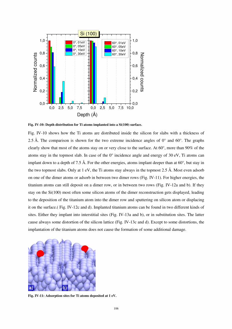
106
Fig. IV-10: Depth distribution for Ti atoms implanted into a Si(100) surface.
Fig. IV-10 shows how the Ti atoms are distributed inside the silicon for slabs with a thickness of
2.5 Å. The comparison is shown for the two extreme incidence angles of 0° and 60°. The graphs
clearly show that most of the atoms stay on or very close to the surface. At 60°, more than 90% of the
atoms stay in the topmost slab. In case of the 0° incidence angle and energy of 30 eV, Ti atoms can
implant down to a depth of 7.5 Å. For the other energies, atoms implant deeper than at 60°, but stay in
the two topmost slabs. Only at 1 eV, the Ti atoms stay always in the topmost 2.5 Å. Most even adsorb
on one of the dimer atoms or adsorb in between two dimer rows (Fig. IV-11). For higher energies, the
titanium atoms can still deposit on a dimer row, or in between two rows (Fig. IV-12a and b). If they
stay on the Si(100) most often some silicon atoms of the dimer reconstruction gets displayed, leading
to the deposition of the titanium atom into the dimer row and sputtering on silicon atom or displacing
it on the surface.( Fig. IV-12c and d). Implanted titanium atoms can be found in two different kinds of
sites. Either they implant into interstitial sites (Fig. IV-13a and b), or in substitution sites. The latter
cause always some distortion of the silicon lattice (Fig. IV-13c and d). Except to some distortions, the
implantation of the titanium atoms does not cause the formation of some additional damage.
Fig. IV-11: Adsorption sites for Ti atoms deposited at 1 eV.
0,0 2,5 5,0 7,50,0
0,2
0,4
0,6
0,8
1,0
Nor
mal
ized
cou
nts
Depth (Å)
0°, 01eV 0°, 05eV 0°, 10eV 0°, 30eV
0,0 2,5 5,0 7,5 10,00,0
0,2
0,4
0,6
0,8
1,0 60°, 01eV 60°, 05eV 60°, 10eV 60°, 30eV
Norm
alized counts
Si (100)
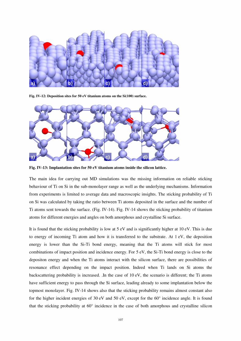
107
Fig. IV-12: Deposition sites for 50 eV titanium atoms on the Si(100) surface.
Fig. IV-13: Implantation sites for 50 eV titanium atoms inside the silicon lattice.
The main idea for carrying out MD simulations was the missing information on reliable sticking
behaviour of Ti on Si in the sub-monolayer range as well as the underlying mechanisms. Information
from experiments is limited to average data and macroscopic insights. The sticking probability of Ti
on Si was calculated by taking the ratio between Ti atoms deposited in the surface and the number of
Ti atoms sent towards the surface. (Fig. IV-14). Fig. IV-14 shows the sticking probability of titanium
atoms for different energies and angles on both amorphous and crystalline Si surface.
It is found that the sticking probability is low at 5 eV and is significantly higher at 10 eV. This is due
to energy of incoming Ti atom and how it is transferred to the substrate. At 1 eV, the deposition
energy is lower than the Si-Ti bond energy, meaning that the Ti atoms will stick for most
combinations of impact position and incidence energy. For 5 eV, the Si-Ti bond energy is close to the
depositon energy and when the Ti atoms interact with the silicon surface, there are possibilities of
resonance effect depending on the impact position. Indeed when Ti lands on Si atoms the
backscattering probability is increased. .In the case of 10 eV, the scenario is different; the Ti atoms
have sufficient energy to pass through the Si surface, leading already to some implantation below the
topmost monolayer. Fig. IV-14 shows also that the sticking probability remains almost constant also
for the higher incident energies of 30 eV and 50 eV, except for the 60° incidence angle. It is found
that the sticking probability at 60° incidence in the case of both amorphous and crystalline silicon
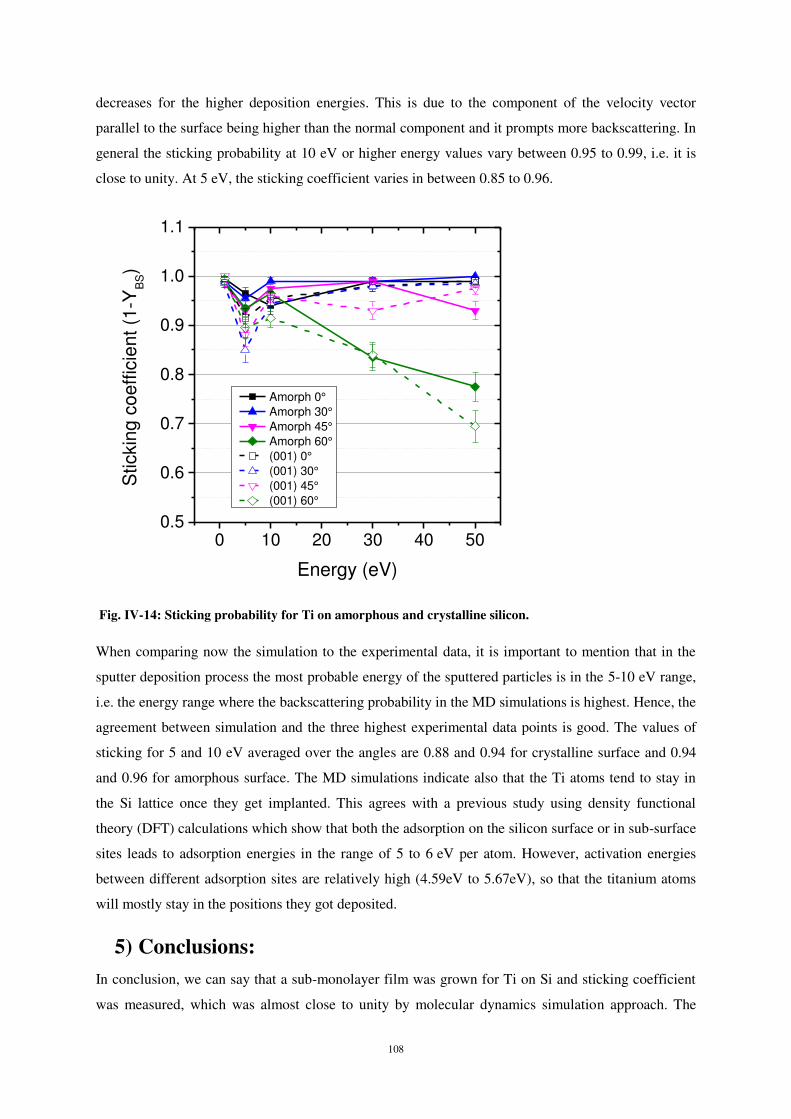
108
decreases for the higher deposition energies. This is due to the component of the velocity vector
parallel to the surface being higher than the normal component and it prompts more backscattering. In
general the sticking probability at 10 eV or higher energy values vary between 0.95 to 0.99, i.e. it is
close to unity. At 5 eV, the sticking coefficient varies in between 0.85 to 0.96.
Fig. IV-14: Sticking probability for Ti on amorphous and crystalline silicon.
When comparing now the simulation to the experimental data, it is important to mention that in the
sputter deposition process the most probable energy of the sputtered particles is in the 5-10 eV range,
i.e. the energy range where the backscattering probability in the MD simulations is highest. Hence, the
agreement between simulation and the three highest experimental data points is good. The values of
sticking for 5 and 10 eV averaged over the angles are 0.88 and 0.94 for crystalline surface and 0.94
and 0.96 for amorphous surface. The MD simulations indicate also that the Ti atoms tend to stay in
the Si lattice once they get implanted. This agrees with a previous study using density functional
theory (DFT) calculations which show that both the adsorption on the silicon surface or in sub-surface
sites leads to adsorption energies in the range of 5 to 6 eV per atom. However, activation energies
between different adsorption sites are relatively high (4.59eV to 5.67eV), so that the titanium atoms
will mostly stay in the positions they got deposited.
5) Conclusions: In conclusion, we can say that a sub-monolayer film was grown for Ti on Si and sticking coefficient
was measured, which was almost close to unity by molecular dynamics simulation approach. The
0 10 20 30 40 500.5
0.6
0.7
0.8
0.9
1.0
1.1
Amorph 0° Amorph 30° Amorph 45° Amorph 60° (001) 0° (001) 30° (001) 45° (001) 60°
Stic
king
coe
ffici
ent (
1-Y
BS)
Energy (eV)
109
experimental sticking coefficient has on average a fluctuation. As we discussed, there were possible
amount of uncertainty during the measurement of sticking coefficient in experimental approach,
otherwise we expect sticking coefficient to be more or less constant in the sub-monolayer range and to
change for a larger coverage. The method we employed here for the measurement of sticking
coefficient is quite large in steps and involves mathematical and statistical estimations. Somehow we
are able to estimate the sticking coefficient but improving the system set up and reducing the error,
more reliable sticking values can be achieved.
The conditions in experiments and simulations were also not exactly the same. Modelling the
deposition of titanium up to the coverage reached in the experimental work would have been a tedious
job and there was no time left for the optimisation of Ti-Ti interaction parameters to make such
multiple Ti depositions. But at least single Ti depositions give us an insight into the behaviour of
sticking of Ti while the angles and energies are changed keeping the flux in a constant rate.

110
111
W deposition on Si
“Sticking and deposition mechanism of tungsten
on silicon surfaces has been investigated by
storing matter technique as well as by numerical
simulations.”

112
113
Chapitre 5.
Tungsten (W) deposition on Silicon (Si)
1) Introduction: Here in this chapter we will discuss about the deposition process of sub-monolayer tungsten (W) film
at room temperature by the storing matter technique by changing the fluence of argon ions during the
deposition process. Later the deposited tungsten sub-monolayer film has been analysed in secondary
ion mass spectrometry instrument to estimate the deposition and sticking behaviour of tungsten on
silicon surface. The key parameters for making deposit in storing matter technique are chosen to
achieve sub-monolayer deposits. The parameters in SIMS analysis are chosen also cautiously to get
low sputter rates as the deposits are dilute. The ejected sputtered particles are spread over a certain
area of the collector to form the deposit. Like titanium deposits, in order to investigate the distribution
of the atoms in the collector surface, several dynamic SIMS analyses were done across the deposit
along vertical and horizontal directions to find the centre of the deposit and record its shapes. A
maximum intensity is always found almost at the edge of the collector for tungsten deposits. The
silicon (Si) collector used for making tungsten deposit is same as for the titanium deposit described in
previous chapter and also the cleaning procedures of silicon collectors is similar as before. One 10
mm x 15 mm foil of tungsten was used as a target.
Along with the experimental deposition process, molecular dynamics investigation for deposition and
implantation mechanism of tungsten atoms in silicon structure have been done by post-doc researcher
using the Kieffer force field. The sticking and deposition behaviour of the tungsten atoms in silicon
have been investigated by depth distribution, mean depth variations, lateral displacement, sticking
probability calculations using MD simulations. The details of the MD results will be given in later
section of this chapter after experimental results.
2) Experimental setup
i) Storing matter conditions for W deposits
The storing matter conditions to achieve W deposits are the same as those used in the case of titanium
(cf Table II-6 in chapter 2), except the fluency of incoming atoms. During the tungsten deposition
preparation, the intensity of the raster-scanned Ar+ beam has been varied from 100 nA to 160 nA and
the deposition time from 200 s to 480 s in order to change the primary ion fluence from1.62 x 1014 to
4.80 x 10¹⁴ ions/cm2. This corresponds to 9.26 x 10¹⁴ to 2.73 x 10¹⁵sputtered tungsten atoms. For all
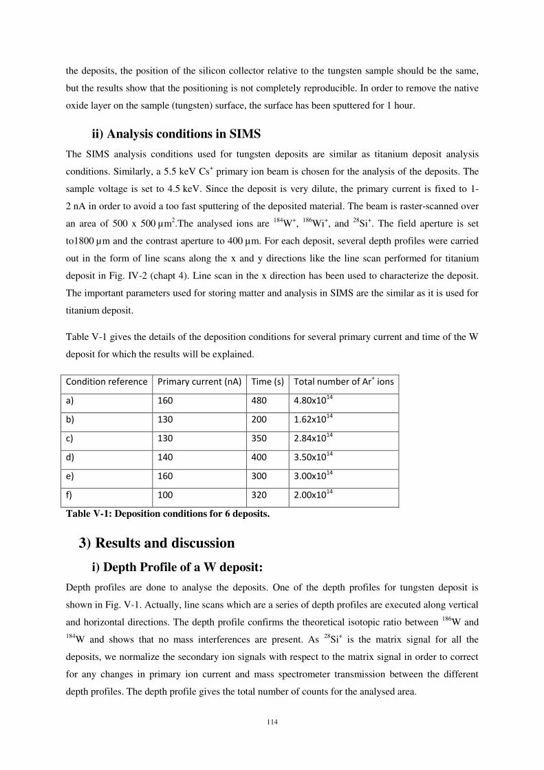
114
the deposits, the position of the silicon collector relative to the tungsten sample should be the same,
but the results show that the positioning is not completely reproducible. In order to remove the native
oxide layer on the sample (tungsten) surface, the surface has been sputtered for 1 hour.
ii) Analysis conditions in SIMS
The SIMS analysis conditions used for tungsten deposits are similar as titanium deposit analysis
conditions. Similarly, a 5.5 keV Cs+ primary ion beam is chosen for the analysis of the deposits. The
sample voltage is set to 4.5 keV. Since the deposit is very dilute, the primary current is fixed to 1-
2 nA in order to avoid a too fast sputtering of the deposited material. The beam is raster-scanned over
an area of 500 x 500 µm2.The analysed ions are 184W+, 186Wi+, and 28Si+. The field aperture is set
to1800 µm and the contrast aperture to 400 µm. For each deposit, several depth profiles were carried
out in the form of line scans along the x and y directions like the line scan performed for titanium
deposit in Fig. IV-2 (chapt 4). Line scan in the x direction has been used to characterize the deposit.
The important parameters used for storing matter and analysis in SIMS are the similar as it is used for
titanium deposit.
Table V-1 gives the details of the deposition conditions for several primary current and time of the W
deposit for which the results will be explained.
Condition reference Primary current (nA) Time (s) Total number of Ar+ ions
a) 160 480 4.80x10¹⁴
b) 130 200 1.62x10¹⁴
c) 130 350 2.84x10¹⁴
d) 140 400 3.50x10¹⁴
e) 160 300 3.00x10¹⁴
f) 100 320 2.00x10¹⁴
Table V-1: Deposition conditions for 6 deposits.
3) Results and discussion
i) Depth Profile of a W deposit:
Depth profiles are done to analyse the deposits. One of the depth profiles for tungsten deposit is
shown in Fig. V-1. Actually, line scans which are a series of depth profiles are executed along vertical
and horizontal directions. The depth profile confirms the theoretical isotopic ratio between 186W and 184W and shows that no mass interferences are present. As 28Si+ is the matrix signal for all the
deposits, we normalize the secondary ion signals with respect to the matrix signal in order to correct
for any changes in primary ion current and mass spectrometer transmission between the different
depth profiles. The depth profile gives the total number of counts for the analysed area.
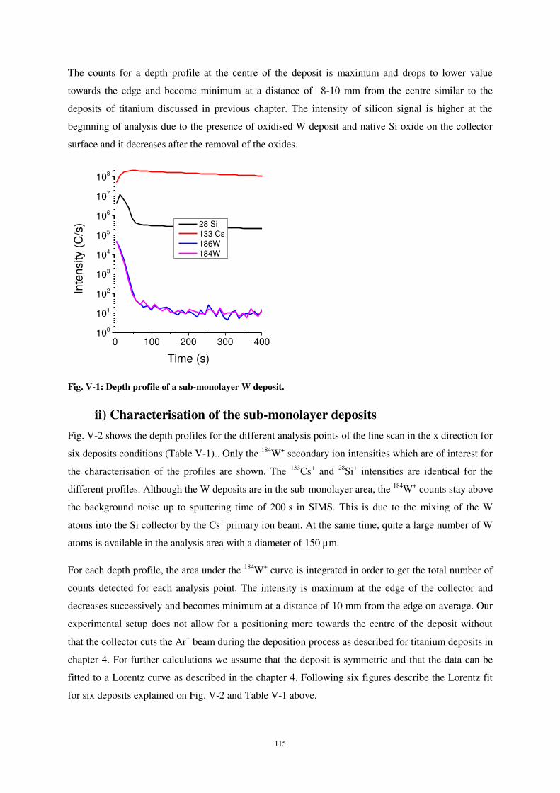
115
The counts for a depth profile at the centre of the deposit is maximum and drops to lower value
towards the edge and become minimum at a distance of 8-10 mm from the centre similar to the
deposits of titanium discussed in previous chapter. The intensity of silicon signal is higher at the
beginning of analysis due to the presence of oxidised W deposit and native Si oxide on the collector
surface and it decreases after the removal of the oxides.
Fig. V-1: Depth profile of a sub-monolayer W deposit.
ii) Characterisation of the sub-monolayer deposits
Fig. V-2 shows the depth profiles for the different analysis points of the line scan in the x direction for
six deposits conditions (Table V-1).. Only the 184W+ secondary ion intensities which are of interest for
the characterisation of the profiles are shown. The 133Cs+ and 28Si+ intensities are identical for the
different profiles. Although the W deposits are in the sub-monolayer area, the 184W+ counts stay above
the background noise up to sputtering time of 200 s in SIMS. This is due to the mixing of the W
atoms into the Si collector by the Cs+ primary ion beam. At the same time, quite a large number of W
atoms is available in the analysis area with a diameter of 150 µm.
For each depth profile, the area under the 184W+ curve is integrated in order to get the total number of
counts detected for each analysis point. The intensity is maximum at the edge of the collector and
decreases successively and becomes minimum at a distance of 10 mm from the edge on average. Our
experimental setup does not allow for a positioning more towards the centre of the deposit without
that the collector cuts the Ar+ beam during the deposition process as described for titanium deposits in
chapter 4. For further calculations we assume that the deposit is symmetric and that the data can be
fitted to a Lorentz curve as described in the chapter 4. Following six figures describe the Lorentz fit
for six deposits explained on Fig. V-2 and Table V-1 above.
0 100 200 300 400100
101
102
103
104
105
106
107
108
Inte
nsity
(C
/s)
Time (s)
28 Si 133 Cs 186W 184W
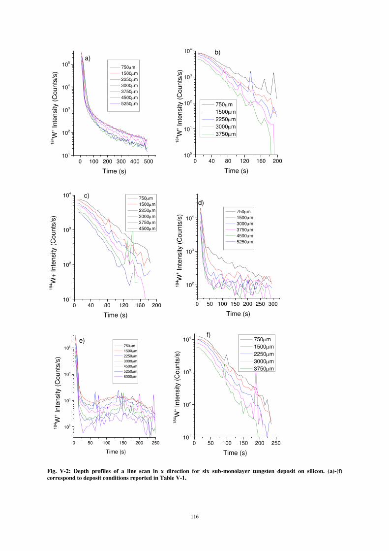
116
Fig. V-2: Depth profiles of a line scan in x direction for six sub-monolayer tungsten deposit on silicon. (a)-(f) correspond to deposit conditions reported in Table V-1.
0 100 200 300 400 500101
102
103
104
105a)
184 W
+ Inte
nsity
(C
ount
s/s)
Time (s)
750m 1500m 2250m 3000m 3750m 4500m 5250m
0 50 100 150 200 250 300
102
103
104
d)
184 W
+ Inte
nsity
(C
ount
s/s)
Time (s)
750m 1500m 3000m 3750m 4500m 5250m
0 40 80 120 160 200101
102
103
104 c)
184 W
+ In
tens
ity (
Cou
nts/
s)
Time (s)
750m 1500m 2250m 3000m 3750m 4500m
0 40 80 120 160 200100
101
102
103
104b)
184 W
+ Inte
nsity
(C
ount
s/s)
Time (s)
750m 1500m 2250m 3000m 3750m
0 50 100 150 200 250101
102
103
104f)
184 W
+ Inte
nsity
(C
ount
s/s)
Time (s)
750m 1500m 2250m 3000m 3750m
0 50 100 150 200 250
102
103
104
105
e)
184 W
+ Inte
nsity
(C
ount
s/s)
Time (s)
750m 1500m 2250m 3000m 4500m 5250m 6000m
117
Fig. V-3: Lorentz curve fitting in 1D along the distance from the edge of the substrate, where a), b), c), d),
e), and f) correspond to the same profile as in Fig. V-2.
0 1 2 3 4
0.8
1.2
1.6
2.0
2.4 a)
Tot
al 18
4 W+ C
ount
s (x
106 )
Position (mm)
Data Lorentz fit
0 1 2 3 4 5
0.05
0.10
0.15
0.20
0.25
d)
Tot
al 18
4 W+ C
ount
s (x
106 )
Position (mm)
Data Lorentz fit
0 1 2 3 4
0.2
0.3
0.4
0.5
0.6c)
Tot
al 18
4 W+ C
ount
s (x
106 )
Position (mm)
Data Lorentz fit
0.0 0.5 1.0 1.5 2.0 2.5 3.0
0.3
0.4
0.5
0.6
0.7 b)
Tot
al 18
4 W+ C
ount
s (x
106 )
Position (mm)
Data Lorentz fit
0.0 0.5 1.0 1.5 2.0 2.5 3.0
0.4
0.5
0.6
0.7
0.8
0.9
1.0 f)
Tot
al 18
4 W+ C
ount
s (x
106 )
Position (mm)
Data Lorentz fit
0 1 2 3 4
0.2
0.4
0.6
0.8
1.0
1.2
1.4 e)
Tot
al 18
4 W+ C
ount
s (x
106 )
Position (mm)
Data Lorentz fit
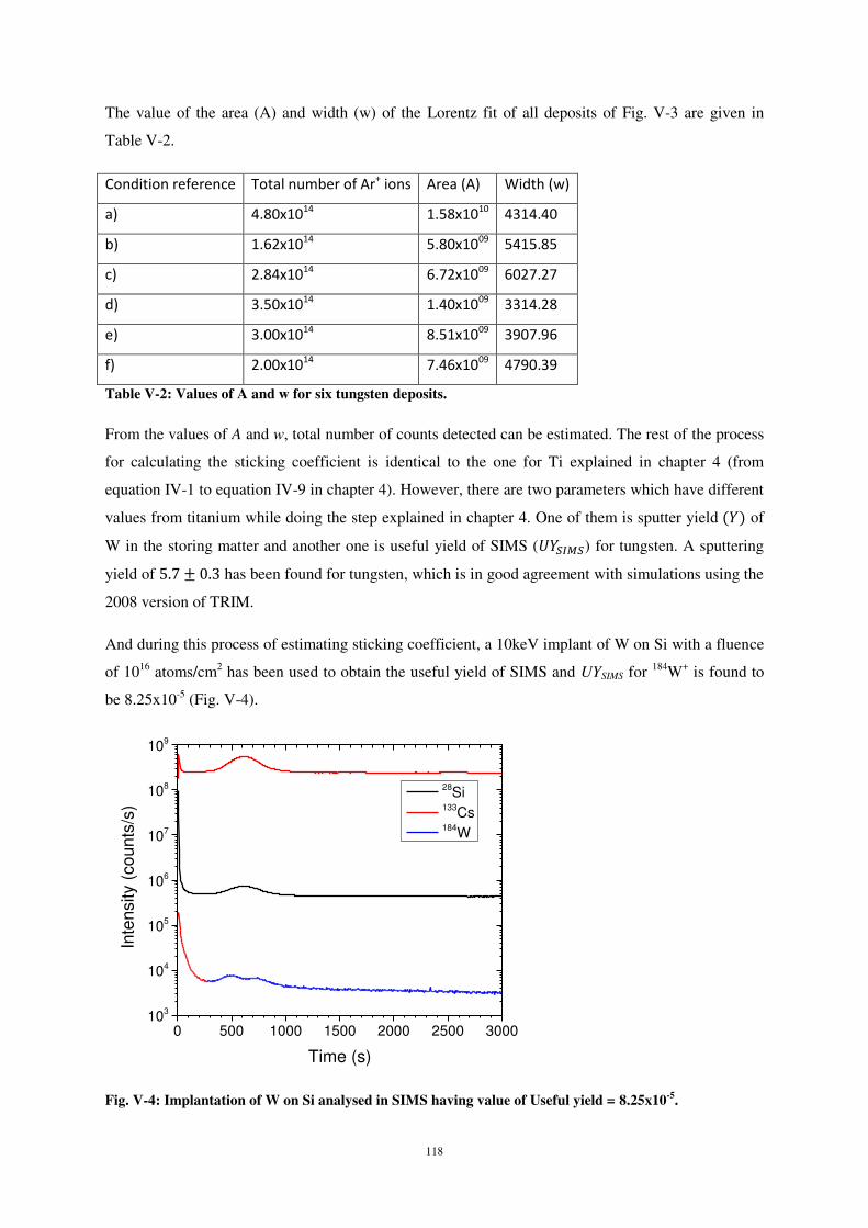
118
The value of the area (A) and width (w) of the Lorentz fit of all deposits of Fig. V-3 are given in
Table V-2.
Condition reference Total number of Ar+ ions Area (A) Width (w)
a) 4.80x10¹⁴
1.58x10¹⁰
4314.40
b) 1.62x10¹⁴
5.80x1009
5415.85
c) 2.84x10¹⁴
6.72x1009
6027.27
d) 3.50x10¹⁴
1.40x1009
3314.28
e) 3.00x10¹⁴
8.51x1009
3907.96
f) 2.00x10¹⁴
7.46x1009
4790.39
Table V-2: Values of A and w for six tungsten deposits.
From the values of A and w, total number of counts detected can be estimated. The rest of the process
for calculating the sticking coefficient is identical to the one for Ti explained in chapter 4 (from
equation IV-1 to equation IV-9 in chapter 4). However, there are two parameters which have different
values from titanium while doing the step explained in chapter 4. One of them is sputter yield of
W in the storing matter and another one is useful yield of SIMS ( ) for tungsten. A sputtering
yield of has been found for tungsten, which is in good agreement with simulations using the
2008 version of TRIM.
And during this process of estimating sticking coefficient, a 10keV implant of W on Si with a fluence
of 1016 atoms/cm2 has been used to obtain the useful yield of SIMS and UYSIMS for 184W+ is found to
be 8.25x10⁻⁵ (Fig. V-4).
Fig. V-4: Implantation of W on Si analysed in SIMS having value of Useful yield = 8.25x10⁻⁵.
0 500 1000 1500 2000 2500 3000103
104
105
106
107
108
109
Inte
nsity
(co
unts
/s)
Time (s)
28Si 133Cs 184W
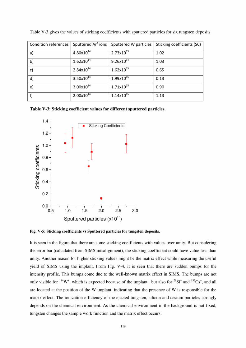
119
Table V-3 gives the values of sticking coefficients with sputtered particles for six tungsten deposits.
Condition references Sputtered Ar+ ions Sputtered W particles Sticking coefficients (SC)
a) 4.80x10¹⁴
2.73x10¹⁵
1.02
b) 1.62x10¹⁴
9.26x10¹⁴
1.03
c) 2.84x10¹⁴
1.62x10¹⁵
0.65
d) 3.50x10¹⁴
1.99x10¹⁵
0.13
e) 3.00x10¹⁴
1.71x10¹⁵
0.90
f) 2.00x10¹⁴
1.14x10¹⁵
1.13
Table V-3: Sticking coefficient values for different sputtered particles.
Fig. V-5: Sticking coefficients vs Sputtered particles for tungsten deposits.
It is seen in the figure that there are some sticking coefficients with values over unity. But considering
the error bar (calculated from SIMS misalignment), the sticking coefficient could have value less than
unity. Another reason for higher sticking values might be the matrix effect while measuring the useful
yield of SIMS using the implant. From Fig. V-4, it is seen that there are sudden bumps for the
intensity profile. This bumps come due to the well-known matrix effect in SIMS. The bumps are not
only visible for 184W+, which is expected because of the implant, but also for 28Si+ and 133Cs+, and all
are located at the position of the W implant, indicating that the presence of W is responsible for the
matrix effect. The ionization efficiency of the ejected tungsten, silicon and cesium particles strongly
depends on the chemical environment. As the chemical environment in the background is not fixed,
tungsten changes the sample work function and the matrix effect occurs.
0.5 1.0 1.5 2.0 2.5 3.00.0
0.2
0.4
0.6
0.8
1.0
1.2
1.4 Sticking Coefficients
Stic
king
coe
ffici
ents
Sputtered particles (x1015)
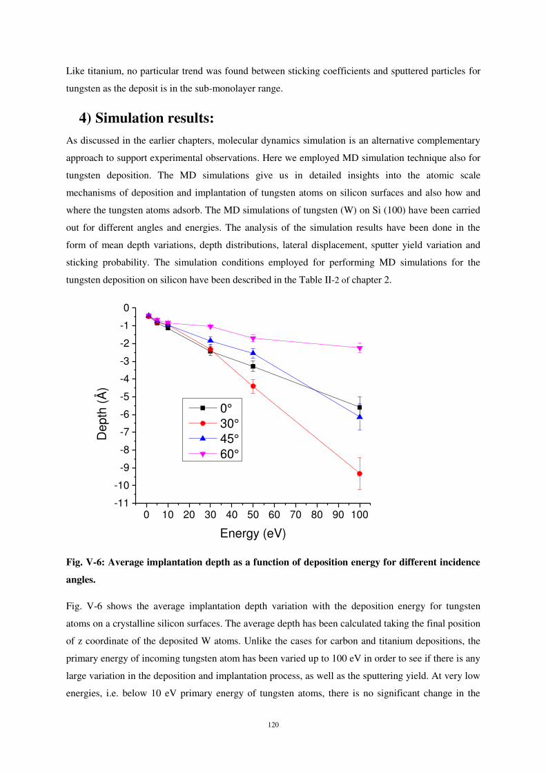
120
Like titanium, no particular trend was found between sticking coefficients and sputtered particles for
tungsten as the deposit is in the sub-monolayer range.
4) Simulation results: As discussed in the earlier chapters, molecular dynamics simulation is an alternative complementary
approach to support experimental observations. Here we employed MD simulation technique also for
tungsten deposition. The MD simulations give us in detailed insights into the atomic scale
mechanisms of deposition and implantation of tungsten atoms on silicon surfaces and also how and
where the tungsten atoms adsorb. The MD simulations of tungsten (W) on Si (100) have been carried
out for different angles and energies. The analysis of the simulation results have been done in the
form of mean depth variations, depth distributions, lateral displacement, sputter yield variation and
sticking probability. The simulation conditions employed for performing MD simulations for the
tungsten deposition on silicon have been described in the Table II-2 of chapter 2.
Fig. V-6: Average implantation depth as a function of deposition energy for different incidence
angles.
Fig. V-6 shows the average implantation depth variation with the deposition energy for tungsten
atoms on a crystalline silicon surfaces. The average depth has been calculated taking the final position
of z coordinate of the deposited W atoms. Unlike the cases for carbon and titanium depositions, the
primary energy of incoming tungsten atom has been varied up to 100 eV in order to see if there is any
large variation in the deposition and implantation process, as well as the sputtering yield. At very low
energies, i.e. below 10 eV primary energy of tungsten atoms, there is no significant change in the
0 10 20 30 40 50 60 70 80 90 100-11
-10
-9
-8
-7
-6
-5
-4
-3
-2
-1
0
Dep
th (
Å)
Energy (eV)
0° 30° 45° 60°
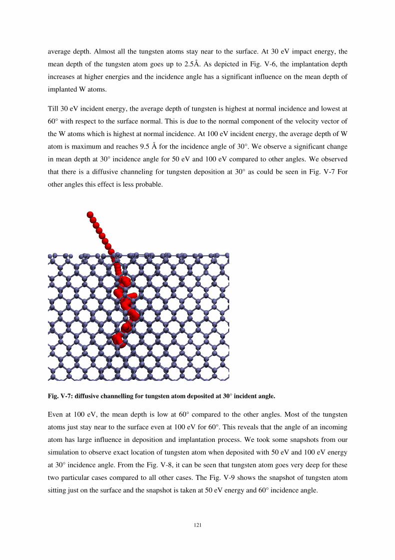
121
average depth. Almost all the tungsten atoms stay near to the surface. At 30 eV impact energy, the
mean depth of the tungsten atom goes up to 2.5Å. As depicted in Fig. V-6, the implantation depth
increases at higher energies and the incidence angle has a significant influence on the mean depth of
implanted W atoms.
Till 30 eV incident energy, the average depth of tungsten is highest at normal incidence and lowest at
60° with respect to the surface normal. This is due to the normal component of the velocity vector of
the W atoms which is highest at normal incidence. At 100 eV incident energy, the average depth of W
atom is maximum and reaches 9.5 Å for the incidence angle of 30°. We observe a significant change
in mean depth at 30° incidence angle for 50 eV and 100 eV compared to other angles. We observed
that there is a diffusive channeling for tungsten deposition at 30° as could be seen in Fig. V-7 For
other angles this effect is less probable.
Fig. V-7: diffusive channelling for tungsten atom deposited at 30° incident angle.
Even at 100 eV, the mean depth is low at 60° compared to the other angles. Most of the tungsten
atoms just stay near to the surface even at 100 eV for 60°. This reveals that the angle of an incoming
atom has large influence in deposition and implantation process. We took some snapshots from our
simulation to observe exact location of tungsten atom when deposited with 50 eV and 100 eV energy
at 30° incidence angle. From the Fig. V-8, it can be seen that tungsten atom goes very deep for these
two particular cases compared to all other cases. The Fig. V-9 shows the snapshot of tungsten atom
sitting just on the surface and the snapshot is taken at 50 eV energy and 60° incidence angle.
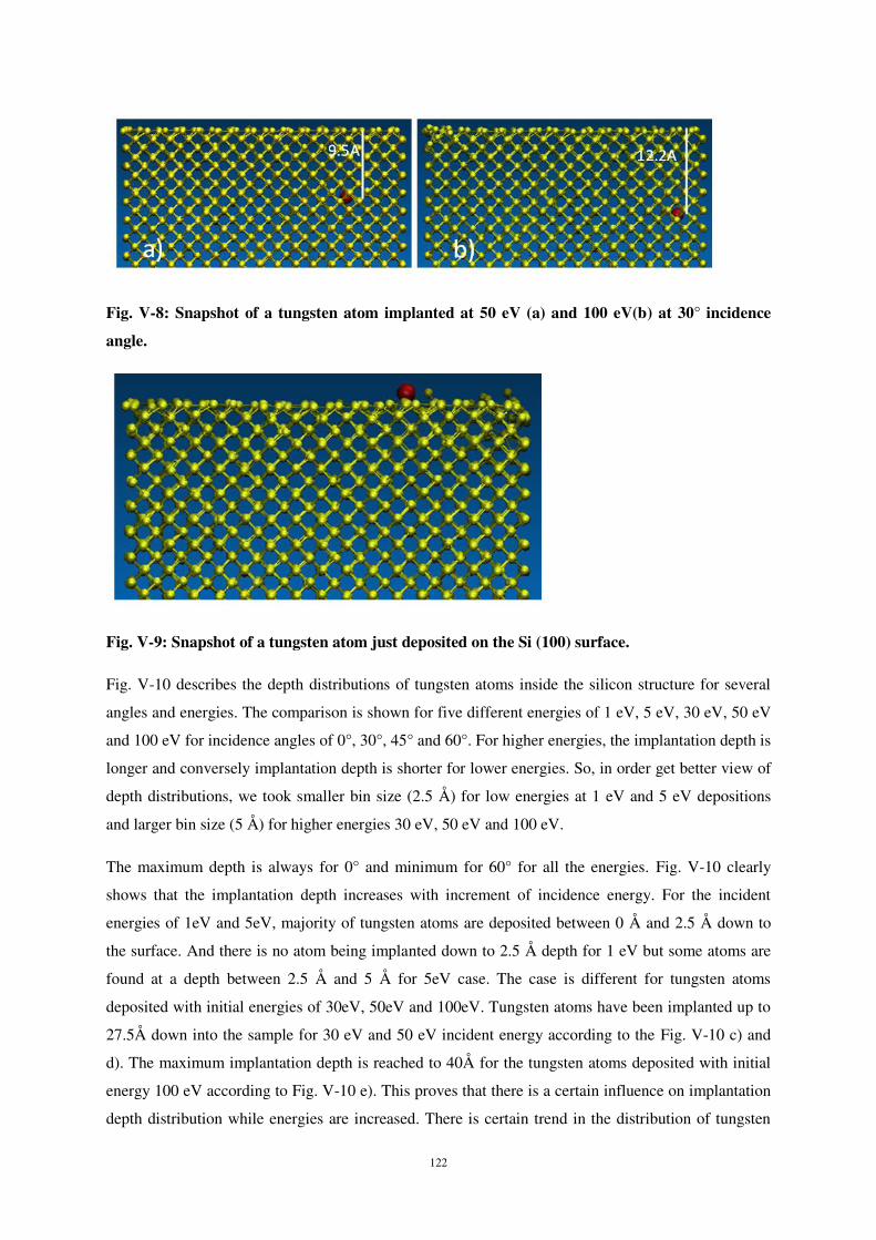
122
Fig. V-8: Snapshot of a tungsten atom implanted at 50 eV (a) and 100 eV(b) at 30° incidence
angle.
Fig. V-9: Snapshot of a tungsten atom just deposited on the Si (100) surface.
Fig. V-10 describes the depth distributions of tungsten atoms inside the silicon structure for several
angles and energies. The comparison is shown for five different energies of 1 eV, 5 eV, 30 eV, 50 eV
and 100 eV for incidence angles of 0°, 30°, 45° and 60°. For higher energies, the implantation depth is
longer and conversely implantation depth is shorter for lower energies. So, in order get better view of
depth distributions, we took smaller bin size (2.5 Å) for low energies at 1 eV and 5 eV depositions
and larger bin size (5 Å) for higher energies 30 eV, 50 eV and 100 eV.
The maximum depth is always for 0° and minimum for 60° for all the energies. Fig. V-10 clearly
shows that the implantation depth increases with increment of incidence energy. For the incident
energies of 1eV and 5eV, majority of tungsten atoms are deposited between 0 Å and 2.5 Å down to
the surface. And there is no atom being implanted down to 2.5 Å depth for 1 eV but some atoms are
found at a depth between 2.5 Å and 5 Å for 5eV case. The case is different for tungsten atoms
deposited with initial energies of 30eV, 50eV and 100eV. Tungsten atoms have been implanted up to
27.5Å down into the sample for 30 eV and 50 eV incident energy according to the Fig. V-10 c) and
d). The maximum implantation depth is reached to 40Å for the tungsten atoms deposited with initial
energy 100 eV according to Fig. V-10 e). This proves that there is a certain influence on implantation
depth distribution while energies are increased. There is certain trend in the distribution of tungsten
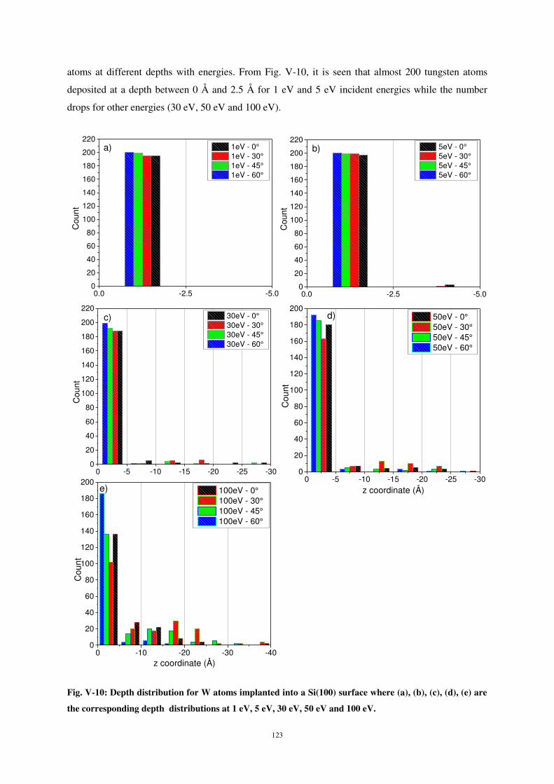
123
atoms at different depths with energies. From Fig. V-10, it is seen that almost 200 tungsten atoms
deposited at a depth between 0 Å and 2.5 Å for 1 eV and 5 eV incident energies while the number
drops for other energies (30 eV, 50 eV and 100 eV).
Fig. V-10: Depth distribution for W atoms implanted into a Si(100) surface where (a), (b), (c), (d), (e) are
the corresponding depth distributions at 1 eV, 5 eV, 30 eV, 50 eV and 100 eV.
0 -5 -10 -15 -20 -25 -300
20
40
60
80
100
120
140
160
180
200d)
Cou
nt
z coordinate (Å)
50eV - 0° 50eV - 30° 50eV - 45° 50eV - 60°
0.0 -2.5 -5.00
20
40
60
80
100
120
140
160
180
200
220b)
Cou
nt
5eV - 0° 5eV - 30° 5eV - 45° 5eV - 60°
0 -10 -20 -30 -400
20
40
60
80
100
120
140
160
180
200e)
Cou
nt
z coordinate (Å)
100eV - 0° 100eV - 30° 100eV - 45° 100eV - 60°
0 -5 -10 -15 -20 -25 -300
20
40
60
80
100
120
140
160
180
200
220
Cou
nt
30eV - 0° 30eV - 30° 30eV - 45° 30eV - 60°
c)
0.0 -2.5 -5.00
20
40
60
80
100
120
140
160
180
200
220a)
Cou
nt
1eV - 0° 1eV - 30° 1eV - 45° 1eV - 60°
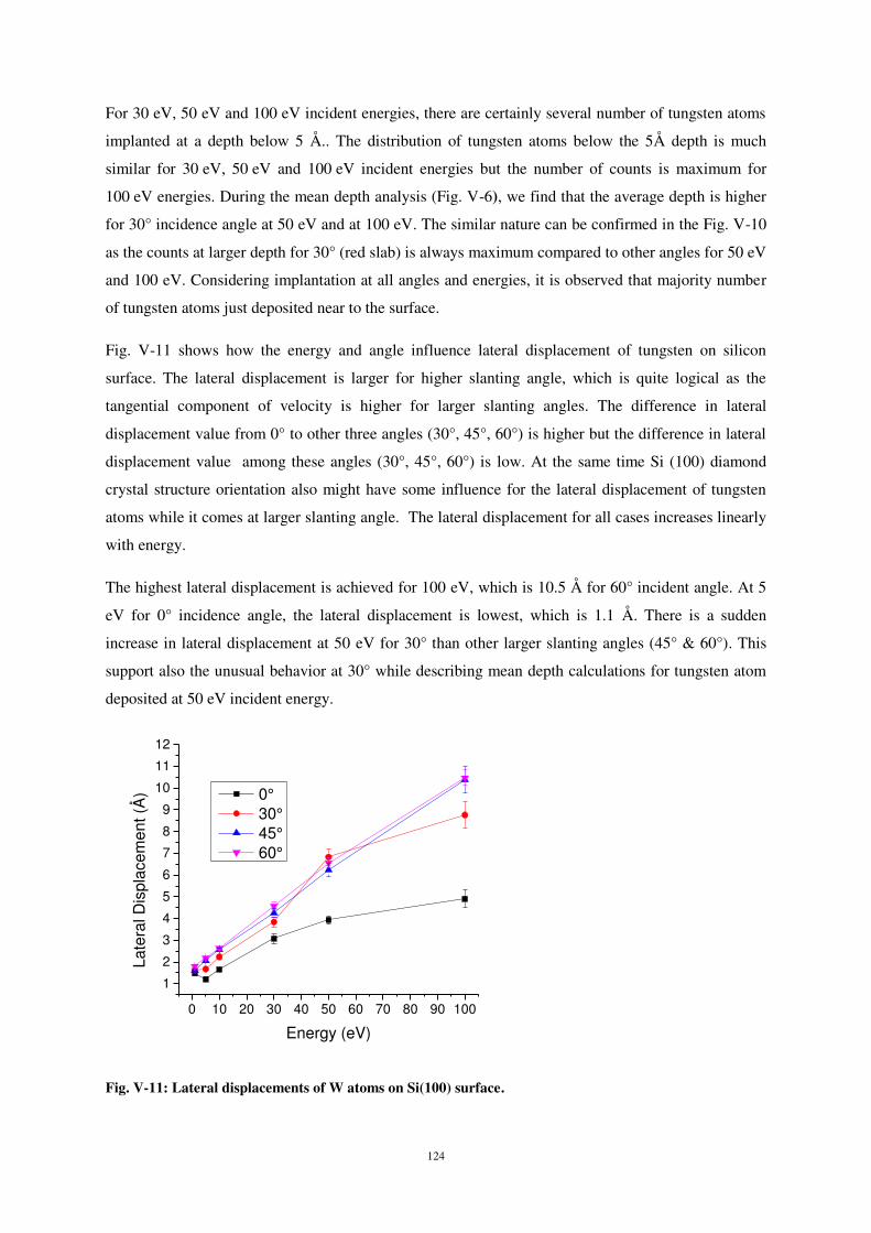
124
For 30 eV, 50 eV and 100 eV incident energies, there are certainly several number of tungsten atoms
implanted at a depth below 5 Å.. The distribution of tungsten atoms below the 5Å depth is much
similar for 30 eV, 50 eV and 100 eV incident energies but the number of counts is maximum for
100 eV energies. During the mean depth analysis (Fig. V-6), we find that the average depth is higher
for 30° incidence angle at 50 eV and at 100 eV. The similar nature can be confirmed in the Fig. V-10
as the counts at larger depth for 30° (red slab) is always maximum compared to other angles for 50 eV
and 100 eV. Considering implantation at all angles and energies, it is observed that majority number
of tungsten atoms just deposited near to the surface.
Fig. V-11 shows how the energy and angle influence lateral displacement of tungsten on silicon
surface. The lateral displacement is larger for higher slanting angle, which is quite logical as the
tangential component of velocity is higher for larger slanting angles. The difference in lateral
displacement value from 0° to other three angles (30°, 45°, 60°) is higher but the difference in lateral
displacement value among these angles (30°, 45°, 60°) is low. At the same time Si (100) diamond
crystal structure orientation also might have some influence for the lateral displacement of tungsten
atoms while it comes at larger slanting angle. The lateral displacement for all cases increases linearly
with energy.
The highest lateral displacement is achieved for 100 eV, which is 10.5 Å for 60° incident angle. At 5
eV for 0° incidence angle, the lateral displacement is lowest, which is 1.1 Å. There is a sudden
increase in lateral displacement at 50 eV for 30° than other larger slanting angles (45° & 60°). This
support also the unusual behavior at 30° while describing mean depth calculations for tungsten atom
deposited at 50 eV incident energy.
Fig. V-11: Lateral displacements of W atoms on Si(100) surface.
0 10 20 30 40 50 60 70 80 90 100
1
2
3
4
5
6
7
8
9
10
11
12
Late
ral D
ispl
acem
ent (
Å)
Energy (eV)
0° 30° 45° 60°
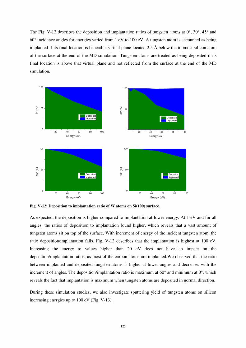
125
The Fig. V-12 describes the deposition and implantation ratios of tungsten atoms at 0°, 30°, 45° and
60° incidence angles for energies varied from 1 eV to 100 eV. A tungsten atom is accounted as being
implanted if its final location is beneath a virtual plane located 2.5 Å below the topmost silicon atom
of the surface at the end of the MD simulation. Tungsten atoms are treated as being deposited if its
final location is above that virtual plane and not reflected from the surface at the end of the MD
simulation.
20 40 60 80 1000
50
100
0° (
%)
Energy (eV)
Deposited Implanted
20 40 60 80 1000
50
100
30°
(%)
Energy (eV)
Deposited Implanted
20 40 60 80 1000
50
100
45°
(%)
Energy (eV)
Deposited Implanted
20 40 60 80 1000
50
100
60°
(%)
Energy (eV)
Deposited Implanted
Fig. V-12: Deposition to implantation ratio of W atoms on Si(100) surface.
As expected, the deposition is higher compared to implantation at lower energy. At 1 eV and for all
angles, the ratios of deposition to implantation found higher, which reveals that a vast amount of
tungsten atoms sit on top of the surface. With increment of energy of the incident tungsten atom, the
ratio deposition/implantation falls. Fig. V-12 describes that the implantation is highest at 100 eV.
Increasing the energy to values higher than 20 eV does not have an impact on the
deposition/implantation ratios, as most of the carbon atoms are implanted.We observed that the ratio
between implanted and deposited tungsten atoms is higher at lower angles and decreases with the
increment of angles. The deposition/implantation ratio is maximum at 60° and minimum at 0°, which
reveals the fact that implantation is maximum when tungsten atoms are deposited in normal direction.
During these simulation studies, we also investigate sputtering yield of tungsten atoms on silicon
increasing energies up to 100 eV (Fig. V-13).
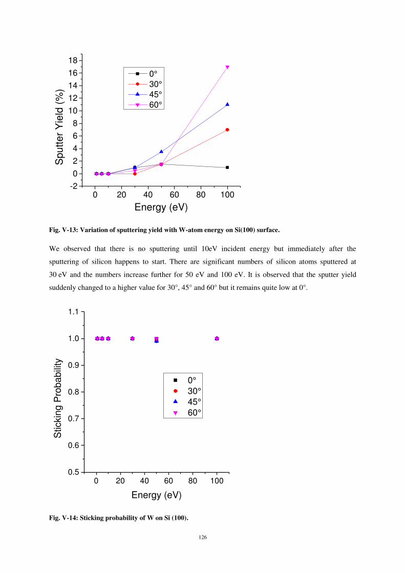
126
Fig. V-13: Variation of sputtering yield with W-atom energy on Si(100) surface.
We observed that there is no sputtering until 10eV incident energy but immediately after the
sputtering of silicon happens to start. There are significant numbers of silicon atoms sputtered at
30 eV and the numbers increase further for 50 eV and 100 eV. It is observed that the sputter yield
suddenly changed to a higher value for 30°, 45° and 60° but it remains quite low at 0°.
Fig. V-14: Sticking probability of W on Si (100).
0 20 40 60 80 100-2
0
2
4
6
8
10
12
14
16
18S
putte
r Y
ield
(%
)
Energy (eV)
0° 30° 45° 60°
0 20 40 60 80 1000.5
0.6
0.7
0.8
0.9
1.0
1.1
0° 30° 45° 60°
Stic
king
Pro
babi
lity
Energy (eV)
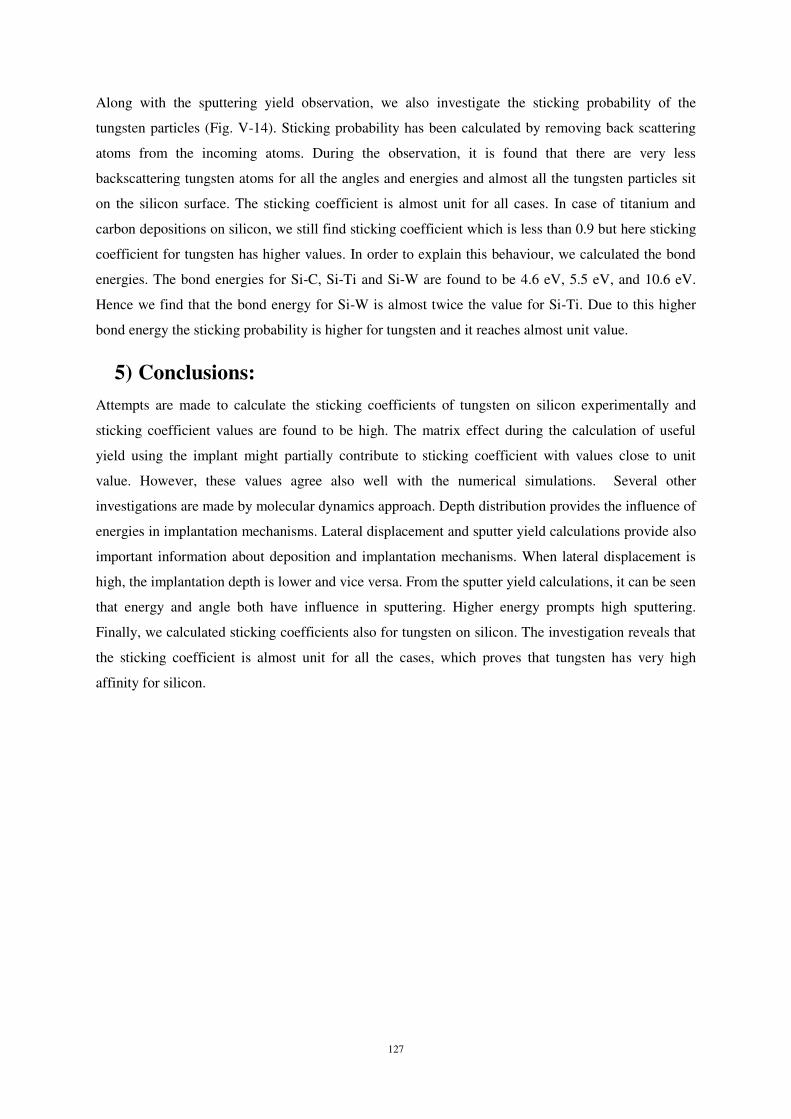
127
Along with the sputtering yield observation, we also investigate the sticking probability of the
tungsten particles (Fig. V-14). Sticking probability has been calculated by removing back scattering
atoms from the incoming atoms. During the observation, it is found that there are very less
backscattering tungsten atoms for all the angles and energies and almost all the tungsten particles sit
on the silicon surface. The sticking coefficient is almost unit for all cases. In case of titanium and
carbon depositions on silicon, we still find sticking coefficient which is less than 0.9 but here sticking
coefficient for tungsten has higher values. In order to explain this behaviour, we calculated the bond
energies. The bond energies for Si-C, Si-Ti and Si-W are found to be 4.6 eV, 5.5 eV, and 10.6 eV.
Hence we find that the bond energy for Si-W is almost twice the value for Si-Ti. Due to this higher
bond energy the sticking probability is higher for tungsten and it reaches almost unit value.
5) Conclusions: Attempts are made to calculate the sticking coefficients of tungsten on silicon experimentally and
sticking coefficient values are found to be high. The matrix effect during the calculation of useful
yield using the implant might partially contribute to sticking coefficient with values close to unit
value. However, these values agree also well with the numerical simulations. Several other
investigations are made by molecular dynamics approach. Depth distribution provides the influence of
energies in implantation mechanisms. Lateral displacement and sputter yield calculations provide also
important information about deposition and implantation mechanisms. When lateral displacement is
high, the implantation depth is lower and vice versa. From the sputter yield calculations, it can be seen
that energy and angle both have influence in sputtering. Higher energy prompts high sputtering.
Finally, we calculated sticking coefficients also for tungsten on silicon. The investigation reveals that
the sticking coefficient is almost unit for all the cases, which proves that tungsten has very high
affinity for silicon.

128
129
Conclusion and Outlook
“This chapter summarises the objectives of the
work and results achieved as well as the
difficulties encountered and future perspectives.”

130
131
Chapitre 6. Conclusion and Outlook
1) Conclusion The sticking, deposition and reorganization of atoms in the sub-monolayer range is of great
importance for the field of surface science. Sticking of any material to a product surface is an
important industrial problem with many applications in the field of packaging, electronic and material
industries In order to well understand the interaction phenomenon between atom and surface, as could
be the case in plasma surface treatments, it is essential to get a perfect knowledge on the sticking
mechanisms during the early stage of interactions since these mechanisms control the interface
properties.
The main goal of this work was to investigate sticking and deposition behaviour of inorganic particles
on silicon surfaces during growth of interface in sub-monolayer regime at few eV energy. Along with
experimental investigations, numerical simulation approach has been used to achieve these objectives.
Large-scale MD simulations making use of first-principles based reactive force fields are used to
understand the atomistic processes underlying the adhesion and reorganization of atoms on the
substrates for numerical approach. Only in this way, a better understanding and control of tailor-
designed surface properties can be obtained.
Furthermore, these studies enhance the comprehension of the deposition process in the sub-monolayer
regime during the collector preparation for the surface analysis technique “Storing Matter”. The
results of Sub-ML give contributions and suggestions to further improve this technique. The
influences of atom and cluster energies and incidence angles on sticking and surface diffusion have
been investigated for different surfaces with respect to surface coverage. The plasma by itself is not
investigated in this project but it is treated as a source of atoms. The major parameters explored in this
project include the particle properties (size, energy and angular distributions) as well as the substrate
composition and roughness.
Sticking and deposition mechanism of C, Ti and W have been studied and discussed by both
experimental and numerical approaches. Along with experimental work, numerical analysis brings
atomic scale insight to deposition and implantation mechanisms. No experimental study has been
carried out for carbon deposition on Si. Experimental observations were not possible for carbon as
with our setup, carbon contaminations could not be reduced to the degree where they did not interfere
significantly with the sub-monolayer deposits. Therefore, additional simulation work has been carried
out for carbon, i.e. the continuous deposition of carbon on silicon.
132
Molecular dynamics investigation of carbon on silicon brings detailed atomic scale insight for carbon
while interacting with silicon at low energies. Continuous carbon deposition along with single impact
of carbon on silicon surfaces describes several aspects of deposition and implantation mechanism for
carbon. The reactive force field developed by John Kieffer is selected, as it permits the formation and
breaking of bonds via an adaptive and environment sensitive charge transfer for both cases. The
results for single carbon deposition mainly consist of mean depth variations, depth distributions,
deposition to implantation ratio, back scattering probability. The comparisons and validations are
made with well-established Erhart-Albe potential for these results. The results using both potentials
are similar, although slight divergences appear at grazing angles and for the higher end of the
deposition energies. The studies of single carbon depositions were extended to multiple carbon
deposition to get a better understanding of carbon deposition and implantation and damage formation
during low-energy carbon atom interactions with a Si(100) surface and also to explain the results in
more experimental prospects as we were not able to execute experimental work for carbon due to
contamination problems. We explained the results in different approaches but the main idea was to
observe and interpret multiple carbon deposition and implantation mechanism at different conditions.
The main parameters to investigate the system structures after continuous deposition include radial
distribution function, depth distribution, coordination calculation, concentration and angular
distribution function.
Radial distribution function along with angular distribution function reveals the damaging information
of Si-C structure as a function of incidence angle, incidence energy, deposition dose and depth in the
sample. It is observed that the structure is heavily distorted just near to the surface and a more ordered
structure at depths exceeding 10 Å. Similar conclusions can be drawn from the concentrations, depth
distributions and coordination number calculations. The influence of angle and energy on the structure
formed has been explained in different sections. It is found that energy has larger influence than angle
for the damage formed. Analysis of the results at different steps varying the incoming dose of carbon
atoms brings also several aspects of deposition and implantation process for carbon. There were some
carbon atoms found even at 15 Å depth at 1 eV, which was mainly due to some deposition induced
diffusion mechanism. Some snapshots were taken to support this phenomenon. Finally, the results of
radial distribution functions, depth distributions, coordination number and angular distributions give
several aspects of deposition and implantation mechanism for continuous carbon depositions. The
results might give some important insight in Si-C bond formation but do not bring complete
information on silicon carbide.
In chapter 4, several aspects regarding sticking and deposition mechanisms for titanium on silicon
have been described and discussed. Experimental observation along with numerical investigation
provides detailed understanding of atomic scale mechanism of titanium on silicon surfaces. Interface
mechanisms during the sub-monolayer film growth have been discussed. Sticking behaviour of
133
titanium during the sub-monolayer film growth has been understood. Experimental investigation of
sticking behaviour does not provide any particular trend with sputtered particles. As could be
expected, it is tricky also to find any particular sticking trend for such a thin deposit. In order to
support these experimental observations, MD simulation studies were carried out. The sticking
coefficient for titanium is found to be higher having values between 0.8 to 0.99. It would have been
more significant to correlate experimental and simulation results if we would have found out sticking
and deposition behaviour of titanium in multiple deposition condition as we studied for carbon
deposition. But optimisation of the Ti-Ti force field parameters would have been a tedious job and
beyond the possibilities of this project. But at least single Ti depositions give us an insight into the
behaviour of sticking of Ti while the angles and energies are changed keeping the flux in a constant
rate.
Similar approaches were considered for the investigation of tungsten deposition behaviour on silicon
substrate. The experimental investigation shows that the values of sticking coefficients are high,
which correlates well with the molecular dynamics studies. One of the reasons for higher sticking
values could be the higher bond energy between W-Si. Several other investigations are made by
molecular dynamics approach. Depth distribution provides the influence of energies in implantation
mechanisms. Lateral displacement and sputter yield calculations provide also important information
about deposition and implantation mechanisms. When lateral displacement is high, the implantation
depth is lower and vice versa. From the sputter yield calculations, it can be seen that energy and angle
both have influence in sputtering. Higher energy prompts high sputtering. Finally, we calculated
sticking coefficients also for tungsten on silicon. The investigation reveals that the sticking coefficient
is almost unit for all the cases, which proves that tungsten has very high affinity for silicon.
Globally, it can be concluded that sticking and deposition behaviour of inorganic particles (C/Ti/W)
on silicon surfaces during the growth of interface in sub monolayer range at low energies have been
understood and explored both by experimental and simulation approach. While there are experimental
limits, analyses are explored in simulation approach. Perfect parallelization of conditions for both
simulation and experimental approach was not possible, at least basic ideas regarding deposition and
sticking have been achieved. Among all three materials, tungsten seems to have higher sticking
probability compared to other two (Ti and C) due to its higher bond energy with silicon.
2) Outlook Sticking coefficient values using storing matter and SIMS techniques are determined but more
accuracy can be achieved by reducing the length of the process. In the scale of accuracy, this
experimental techniques used here cannot be competitive to other traditional sticking coefficient
measurement instrument like Rutherford Backscattering method. The main application of the Storing
Matter technique for inorganic samples is quantitative depth profiling. But during doing depth profiles
134
in SIMS, there were always uncertainty to choose the right spot in the deposit. Including a scale in the
collector holder could reduce the error till some extent.
Control of contaminations with the current set-up is too limited for some elements, and only sputter
deposition and analysis in one chamber can reduce the errors. In this way, we can avoid using suitcase
to transfer the samples. Eventually, it will result less contaminations.
While comparing the results by both simulation and experimental approach, there are several
conditions which could be considered carefully. Although we maintain to keep our deposit from
deposition till the analysis process under UHV conditions, still there are always native oxide layers on
silicon surfaces. But while determining simulation conditions, there is no possibility for silicon
surface to be oxidized. While doing simulations, the angles are perfectly defined but there is no
defined angle within the storing matter set up. In fact, all the sputtered particles distribute through a
solid angle. Similarly, the energy of the incoming atom is fixed and defined in simulation process but
the sputtered particles in storing matter have a distribution of energies. For single atom deposition,
only Si-Ti or Si-W interactions are considered and other interactions are neglected, which is not the
same for experimental interaction among particles in storing matter deposit. A perfect alignment
between simulation and experimental conditions could provide more meaningful comparisons of
phenomenon. For carbon deposition, along with single carbon deposition, we have performed
continuous carbon deposition and different conclusions have been made. It would be better also to
execute continuous titanium and tungsten investigation on silicon surface. Although we could expect
the nature of distribution of titanium /tungsten along the silicon slab might be similar like carbon but
several other findings on the film growth could be investigated. For future aspect, these multiple
titanium and tungsten deposition should be carried out in order to have more realistic comparisons
with sputter deposition techniques at low energies.
Using of implant to calculate the useful yield of SIMS was not the best choice to have competitive
results. But there was no other possibility to measure useful yield except the use of implant.
Sometimes matrix effect during the analysis of implant could bring error in measurement of useful
yield of SIMS. MC simulations, MD simulations, Rutherford backscattering processes could be the
alternatives to avoid the use of implant.
This PhD work is an important first step before investigating deposition mechanism of SiC, TiC and
WC on substrate surface, which has several industrial applications. So, as a continuation of this PhD
work, deposition mechanisms of SiC, TiC and WC on Si substrate could be studied next.
For the current work, only single atom deposition in the few eV range has been carried out but future
work on deposition of small clusters of various sizes using molecular dynamics simulations could be
interesting and could be comparable with plasma deposition process.

135
Several other aspects also could be interesting to investigate, such as island formation, diffusion
during physical characterization of the inorganic Storing Matter deposits. This would provide a deeper
insight into the fundamental processes involved in the deposition processes.

136
137
References
1. Graves, D. B.; Jensen, K. F. Continuum model of dc and rf discharges. IEEE Trans. Plasma
Sci. 1986, PS-14 (2), 78-91.
2. Boeuf, J. P. Numerical model of rf glow discharges. Phys. Rev. A 1987, 36 (6), 2782-2792.
3. Hancock, G.; Compton, R. G. Applications of Kinetic Modelling; 1 ed.; Elsevier: 1999.pp. 1-713.
4. Surendra, M.; Graves, D. B. Particle simulations of radio-frequency glow discharges. Plasma
Science, IEEE Transactions on 1991, 19 (2), 144-157.
5. Birdsall, C. K. Particle-in-cell charged-particle simulations, plus Monte Carlo collisions with neutral atoms, PIC-MCC. Plasma Science, IEEE Transactions on 1991, 19 (2), 65-85.
6. Graves, D. B.; Brault, P. Molecular dynamics for low temperature plasma-surface interaction studies. Journal of Physics D-Applied Physics 2009, 42 (19), 194011.
7. Bogaerts, A.; van Straaten, M.; Gijbels, R. Monte Carlo simulation of an analytical glow discharge: motion of electrons, ions and fast neutrals in the cathode dark space. Spectrochimica Acta Part B: Atomic Spectroscopy 1995, 50 (2), 179-196.
8. Bogaerts, A.; Gijbels, R.; Goedheer, W. J. Hybrid Monte-Carlo Fluid Model of A Direct-Current Glow-Discharge. J. Appl. Phys. 1995, 78 (4), 2233-2241.
9. Brault, P.; Range, H.; Toennies, J. P. Molecular beam studies of sticking of oxygen on the Rh(111) surface. J. Chem. Phys. 1997, 106 (21), 8876-8889.
10. Neyts, E.; Bogaerts, A.; Gijbels, R.; Benedikt, J.; van de Sanden, M. C. M. Molecular dynamics simulations for the growth of diamond-like carbon films from low kinetic energy species. Diamond and Related Materials 2004, 13 (10), 1873-1881.
11. Konoplev, V.; Caturla, M. J.; Abril, I.; Gras-Marti, A. Bulk atomic relocation in low-energy collision cascades in silicon: Molecular Dynamics versus Monte Carlo simulations. Nuclear
Instruments and Methods in Physics Research Section B: Beam Interactions with Materials
and Atoms 1994, 90 (1-4), 363-368.
12. Guvenc, Z. B.; Hippler, R.; Jackson, B. Bombardment of Ni(100) surface with low-energy argons: molecular dynamics simulations. Thin Solid Films 2005, 474 (1-2), 346-357.
13. Gleason, K. K.; Wang, K. S.; Chen, M. K.; Reimer, J. A. Monte Carlo simulations of amorphous hydrogenated silicon thin-film growth. Journal of Applied Physics 1987, 61 (8), 2866-2873.
14. McCaughey, M. J.; Kushner, M. J. Simulation of the bulk and surface-properties of amorphous hydrogenated silicon deposited from silane plasmas. J. Appl. Phys. 1989, 65 (1), 186-195.
138
15. Ohira, T.; Ukai, O.; Noda, M. Fundamental processes of microcrystalline silicon film growth: a molecular dynamics study. Surf. Sci. 2000, 458 (1-3), 216-228.
16. Bakos, T.; Valipa, M.; Aydil, E. S.; Maroudas, D. Temperature dependence of precursor-surface interactions in plasma deposition of silicon thin films 8. Chem. Phys. Lett. 2005, 414 (1-3), 61-65.
17. Bakos, T.; Valipa, M. S.; Maroudas, D. Interactions between radical growth precursors on plasma-deposited silicon thin-film surfaces. J. Chem. Phys. 2007, 126 (11), 114704.
18. Pandey, S. C.; Singh, T.; Maroudas, D. On the growth mechanism of plasma deposited amorphous silicon thin films. Appl. Phys. Lett. 2008, 93 (15), 151913.
19. Valipa, M. S.; Sriraman, S.; Aydil, E. S.; Maroudas, D. Atomic-scale analysis of fundamental mechanisms of surface valley filling during plasma deposition of amorphous silicon thin films. Surface Science 2005, 574 (2-3), 123-143.
20. Gordiets, B. F.; Andujar, J. L.; Corbella, C.; Bertran, E. Kinetic model of thin film growth by vapor deposition. Eur. Phys. J. D 2005, 35 (3), 505-511.
21. Rosen, J.; Schneider, J. A.; Larsson, K. Ab initio studies of adsorption and migration surface processes on an alpha-Al2O3 surface. Solid State Commun. 2005, 135 (1-2), 90-94.
22. Wijesundara, M. B. J.; Hanley, L.; Ni, B. R.; Sinnott, S. B. Effects of unique ion chemistry on thin-film growth by plasma-surface interactions. Proceedings of the National Academy of
Sciences of the United States of America 2000, 97 (1), 23-27.
23. Abrams, C. F.; Graves, D. B. Three-dimensional spatiokinetic distributions of sputtered and scattered products of Ar+ and Cu+ impacts onto the Cu surface: Molecular dynamics simulations. IEEE Trans. Plasma Sci. 1999, 27 (5), 1426-1432.
24. Gou, F.; Chen, L. Z. T.; Meng, C.; Qian, Q. Molecular dynamics simulations of reactive etching of SiC by energetic fluorine. Appl. Phys. A-Mater. Sci. Process. 2007, 88 (2), 385-390.
25. Battaile, C. C.; Srolovitz, D. J.; Butler, J. E. A kinetic Monte Carlo method for the atomic-scale simulation of chemical vapor deposition: Application to diamond. J. Appl. Phys. 1997, 82 (12), 6293-6300.
26. Dawnkaski, E. J.; Srivastava, D.; Garrison, B. J. Growth of diamond films on a diamond {001}(2x1):H surface by time dependent Monte Carlo simulations. J. Chem. Phys. 1996, 104 (15), 5997-6008.
27. Brenner, D. W. Empirical potential for hydrocarbons for use in simulating the chemical vapor-deposition of diamond films. Phys. Rev. B 1990, 42 (15), 9458-9471.
28. Gou, F.; Meng, C. L.; Zhouling, Z. T.; Qian, Q. Hydrocarbon film growth by energetic CH3 molecule impact on SiC (001) surface. Appl. Surf. Sci. 2007, 253 (20), 8517-8523.
29. Stillinger, F. H.; Weber, T. A. Computer-simulation of local order in condensed phases of silicon. Phys. Rev. B 1985, 31 (8), 5262-5271.
30. Pailthorpe, B. A.; Mitchell, D.; Bordes, N. S. Thermal diffusion in molecular dynamics simulations of thin film diamond deposition. Thin Solid Films 1998, 332 (1-2), 109-112.
139
31. Samela, J.; Nordlund, K.; Keinonen, J.; Popok, V. N. Comparison of silicon potentials for cluster bombardment simulations. Nucl. Instrum. Methods Phys. Res. B 2007, 255, 253-258.
32. B.A.Helmer; D.B.Graves Molecular dynamics simulations of fluorosilyl species impacting fluorinated silicon surfaces with energies from 0.1 to 100 eV. Journal of Vacuum Science and
Technology A 1997, 15, 2252.
33. Posselt, M.; Gabriel, A. Atomistic simulation of amorphous germanium and its solid phase epitaxial recrystallization. Phys. Rev. B 2009, 80 (4), 045202.
34. Gärtner, K.; Stock, D.; Weber, B.; Betz, G.; Hautala, M.; Hobler, G.; Hou, M.; Arite, S.; Eckstein, W.; Jiménez-Rodríguez, J. J.; Pérez-Martín, A. M. C.; Andribet, E. P.; Konoplev, V.; Gras-Marti, A.; Posselt, M.; Shapiro, M. H.; Tombrello, T. A.; Urbassek, H. M.; Hensel, H.; Yamamura, Y.; Takeuchi, W. Round robin computer simulation of ion transmission through crystalline layers. Nucl. Instrum. Methods Phys. Res. B 1995, 102 (1-4), 183-197.
35. Tersoff, J. New empirical-model for the structural-properties of silicon. Phys. Rev. Lett. 1986, 56 (6), 632-635.
36. Tersoff, J. Empirical interatomic potential for carbon, with applications to amorphous-carbon. Phys. Rev. Lett. 1988, 61 (25), 2879-2882.
37. Brenner, D. W. Empirical potential for hydrocarbons for use in simulating the chemical vapor deposition of diamond films. Physical Review B 1990, 42 (15), 9458.
38. Abell, G. C. Empirical chemical pseudopotential theory of molecular and metallic bonding. Phys. Rev. B 1985, 31 (10), 6184-6196.
39. Ni, B.; Lee, K. H.; Sinnott, S. B. A reactive empirical bond order (REBO) potential for hydrocarbon-oxygen interactions. J. Phys. : Condens. Matter 2004, 16 (41), 7261-7275.
40. Heo, S.; Sinnott, S. B. Computational investigation of the mechanical properties of nanomaterials. Taipei, Taiwan, 2008; pp 438-442.
41. Betz, G.; Husinsky, W. Molecular-Dynamics Studies of Cluster Emission in Sputtering. Nucl.
Instrum. Methods Phys. Res. B 1995, 102 (1-4), 281-292.
42. Hsu, W. D.; Jang, I.; Sinnott, S. B. Computational investigation of the chemical modification of polystyrene through fluorocarbon and hydrocarbon ion beam deposition. Chemistry of
Materials 2006, 18 (4), 914-921.
43. Hu, Y.; Irving, D. L.; Sinnott, S. B. Ion deposition induced modification of carbon nanopeapods: A computational study. Chemical physics letters 2006, 422 (1), 137-141.
44. Jang, I. K.; Sinnott, S. B. Molecular dynamics simulations of the chemical modification of polystyrene through CxFy+ beam deposition. J. Phys. Chem. B 2004, 108 (49), 18993-19001.
45. Jeong, B. W.; Lim, J. K.; Sinnott, S. B. Tensile mechanical behavior of hollow and filled carbon nanotubes under tension or combined tension-torsion. Applied Physics Letters 2007, 90 (2), 023102.
46. van Duin, A. C. T.; Dasgupta, S.; Lorant, F.; Goddard, W. A. ReaxFF: A reactive force field for hydrocarbons. J. Phys. Chem. A 2001, 105 (41), 9396-9409.
140
47. Rappe, A. K.; Goddard, W. A. Charge equilibration for molecular-dynamics simulations. J.
Phys. Chem. 1991, 95 (8), 3358-3363.
48. Chenoweth, K.; Cheung, S.; van Duin, A. C. T.; Goddard, W. A.; Kober, E. M. Simulations on the thermal decomposition of a poly(dimethylsiloxane) polymer using the ReaxFF reactive force field. J. Am. Chem. Soc. 2005, 127 (19), 7192-7202.
49. van Duin, A. C. T.; Strachan, A.; Stewman, S.; Zhang, Q. S.; Xu, X.; Goddard, W. A. ReaxFF(SiO) reactive force field for silicon and silicon oxide systems. J. Phys. Chem. A 2003, 107 (19), 3803-3811.
50. Cheung, S.; Deng, W. Q.; van Duin, A. C. T.; Goddard, W. A. ReaxFF(MgH) reactive force field for magnesium hydride systems. J. Phys. Chem. A 2005, 109 (5), 851-859.
51. Goddard, W. A.; Zhang, Q.; Uludogan, M.; Strachan, A.; Cagin, T. The ReaxFF polarizable
reactive force fields for molecular dynamics simulation of ferroelectrics. IOP Institute of physics publishing LTD: 2002; pp 45-55.
52. Ludwig, J.; Vlachos, D. G.; van Duin, A. C. T.; Goddard, W. A. Dynamics of the dissociation of hydrogen on stepped platinum surfaces using the ReaxFF reactive force field. J. Phys.
Chem. B 2006, 110 (9), 4274-4282.
53. Liu, B.; Lusk, M. T.; Ely, J. F.; van Duin, A. C. T.; Goddard, W. A. Reactive molecular dynamics force field for the dissociation of light hydrocarbons on Ni(111). Molecular
Simulation 2008, 34 (10-15), 967-972.
54. Jarvi, T. T.; Kuronen, A.; Hakala, M.; Nordlund, K.; van Duin, A. C. T.; Goddard III, W. A.; Jacob, T. Development of a ReaxFF description for gold. The European Physical Journal B 2008, 66 (1), 75-79.
55. Chenoweth, K.; van Duin, A. C. T.; Goddard, W. A. ReaxFF reactive force field for molecular dynamics simulations of hydrocarbon oxidation. J. Phys. Chem. A 2008, 112 (5), 1040-1053.
56. Chenoweth, K.; van Duin, A. C. T.; Persson, P.; Cheng, M. J.; Oxgaard, J.; Goddard, W. A. Development and application of a ReaxFF reactive force field for oxidative dehydrogenation on vanadium oxide catalysts. J. Phys. Chem. C 2008, 112 (37), 14645-14654.
57. Nielson, K. D.; van Duin, A. C. T.; Oxgaard, J.; Deng, W. Q.; Goddard, W. A. Development of the ReaxFF reactive force field for describing transition metal catalyzed reactions, with application to the initial stages of the catalytic formation of carbon nanotubes. J. Phys. Chem.
A 2005, 109 (3), 493-499.
58. Yu, J. G.; Phillpot, S. R.; Sinnott, S. B. Interatomic potential for the structure and energetics of tetrahedrally coordinated silica polymorphs. Phys. Rev. B 2007, 75 (23), 233203.
59. Yu, J. G.; Sinnott, S. B.; Phillpot, S. R. Charge optimized many-body potential for the Si/SiO2 system. Phys. Rev. B 2007, 75 (8), 085311.
60. Yasukawa, A. Using an extended Tersoff interatomic potential to analyze the static-fatigue strength of SiO2 under atmospheric influence. Jsme International Journal Series A-
Mechanics and Material Engineering 1996, 39 (3), 313-320.
141
61. Huang, L. P.; Kieffer, J. Molecular dynamics study of cristobalite silica using a charge transfer three-body potential: Phase transformation and structural disorder. J. Chem. Phys. 2003, 118 (3), 1487-1498.
62. Huang, L. P.; Durandurdu, M.; Kieffer, J. Transformation pathways of silica under high pressure. Nature Materials 2006, 5 (12), 977-981.
63. Huang, L. P.; Kieffer, J. Thermomechanical anomalies and polyamorphism in B2O3 glass: A molecular dynamics simulation study. Phys. Rev. B 2006, 74 (22), 224107.
64. Huang, L. P.; Durandurdu, M.; Kieffer, J. New B2O3 crystals predicted from concurrent molecular dynamics simulations and first-principles calculations. J. Phys. Chem. C 2007, 111 (37), 13712-13720.
65. Huang, L.; Nicholas, J.; Kieffer, J.; Bass, J. Polyamorphic transitions in vitreous B2O3 under pressure. J. Phys. : Condens. Matter 2008, 20 (7), 075107.
66. Bhattacharya, S.; Kieffer, J. Fractal dimensions of silica gels generated using reactive molecular dynamics simulations. J. Chem. Phys. 2005, 122 (9), 094715.
67. Bhattacharya, S.; Kieffer, J. Fractal dimensions of silica gels generated using reactive molecular dynamics simulations. The Journal of chemical physics 2005, 122 (9), 094715.
68. Huang, L. P.; Kieffer, J. Amorphous-amorphous transitions in silica glass. II. Irreversible transitions and densification limit. Phys. Rev. B 2004, 69 (22), 224204.
69. Huang, L. P.; Kieffer, J. Amorphous-amorphous transitions in silica glass. I. Reversible transitions and thermomechanical anomalies. Phys. Rev. B 2004, 69 (22), 224203.
70. Zhou, J.; Kieffer, J. Molecular dynamics simulations of monofunctionalized polyhedral oligomeric silsesquioxane C6H13(H7Si8O 12). Journal of Physical Chemistry C 2008, 112 (10), 3473-3481.
71. Gilmore, C. M.; Sprague, J. A. Molecular-dynamics simulation of the energetic deposition of Ag thin films. Phys. Rev. B 1991, 44 (16), 8950-8957.
72. Sprague, J. A.; Gilmore, C. M. Molecular dynamics simulations of film-substrate interface mixing in the energetic deposition of fcc metals. Thin Solid Films 1996, 272 (2), 244-254.
73. Schwebel, C.; Pellet, C.; Gautherin, G. Angular distributions of heavy particles emitted from a Si target during an ion beam sputter process. Nuclear Instruments and Methods in Physics
Research Section B: Beam Interactions with Materials and Atoms 1986, 18 (1), 525-528.
74. Tarus, J.; Nordlund, K. Molecular dynamics study on Si20 cluster deposition on Si(001). Nuclear Instruments and Methods in Physics Research Section B: Beam Interactions with
Materials and Atoms 2003, 212 (0), 281-285.
75. Biswas, R.; Grest, G. S.; Soukoulis, C. M. Molecular-dynamics simulation of cluster and atom deposition on silicon (111). Phys. Rev. B 1988, 38 (12), 8154-8162.
76. Betz, G.; Husinsky, W. A combined molecular dynamics and kinetic Monte Carlo calculation to study sputter erosion and beam assisted deposition. Nuclear Instruments and Methods in
Physics Research Section B: Beam Interactions with Materials and Atoms 2002, 193 (1-4), 352-358.
142
77. Ju, S. P.; Weng, C. I.; Chang, J. G.; Hwang, C. C. A molecular dynamics study of deposition rate dependence of film morphology in the sputtering process. Surface and Coatings
Technology 2002, 149 (2-3), 135-142.
78. Hu, Y.; Sinnott, S. B. A molecular dynamics study of thin-film formation via molecular cluster beam deposition: effect of incident species. Surface Science 2003, 526 (3), 230-242.
79. Hui Qing Lan; Zheng Ling Kang Molecular Dynamics Simulations of Structures of Amorphous Carbon Films via Deposition. Advanced Materials Research 2011, 194-196, 2220-2224.
80. Chen, H.; Hagiwara, I.; Kiet Tieu, A.; Kishimoto, K.; Liu, Q. Theoretical investigation about secondary deposition of thin-film formation by molecular dynamics simulation. Journal of
Crystal Growth 2007, 303 (2), 530-536.
81. Ishikawa, Y.; Mateo, J. J.; Tryk, D. A.; Cabrera, C. R. Direct molecular dynamics and density-functional theoretical study of the electrochemical hydrogen oxidation reaction and underpotential deposition of H on Pt (111). Journal of Electroanalytical Chemistry 2007, 607 (1), 37-46.
82. Zaminpayma, E.; Nayebi, P.; Mirabbaszadeh, K. A Study About Nanocluster Deposition of Thin-film Formation by Molecular Dynamics Simulation. J Clust Sci 2008, 19 (4), 623-629.
83. Lee, S. G.; Choi, H.; Chung, Y. C. Molecular dynamics simulation of film growth characterization of Fe and Cu on Cu(111) surface in the early stages of the deposition process. Current Applied Physics 2011, 11 (4, Supplement), S65-S68.
84. Zhang, H.; Xia, Z. N. Molecular dynamics simulation of cluster beam Al deposition on Si (100) substrate. Nuclear Instruments and Methods in Physics Research Section B: Beam
Interactions with Materials and Atoms 2000, 160 (3), 372-376.
85. Fang, T. H.; Chang, W. J.; Lin, C. M.; Lien, W. C. Molecular dynamics and experimental studies on deposition mechanisms of ion beam sputtering. Applied Surface Science 2008, 254 (11), 3436-3441.
86. Tomasch, G. A.; Kim, Y. W.; Markert, L. C.; Lee, N. E.; Greene, J. E. Growth of homoepitaxial Ge(001)2 x 1 by ultrahigh vacuum ion beam sputter deposition. Thin Solid
Films 1993, 223 (2), 212-217.
87. K.Miyake; K.Ohashi Superior Corrosion Resistance of Ion Beam Deposited Iron Film. Japanese Journal of Applied Physics 1993, 32, L120.
88. Jimenez-Saez, J. C.; Perez-Martin, A. M. C.; Said-Ettaoussi, M.; Jiménez-Rodríguez, J. J. Molecular dynamics simulation of Ni cluster deposition on Cu(0 0 1) surfaces. Nuclear
Instruments and Methods in Physics Research Section B: Beam Interactions with Materials
and Atoms 2005, 228 (1-4), 64-68.
89. Bunnik, B. S.; de Hoog, C.; Haddeman, E. F. C.; Thijsse, B. J. Molecular dynamics study of Cu deposition on Mo and the effects of low-energy ion irradiation. Nuclear Instruments and
Methods in Physics Research Section B: Beam Interactions with Materials and Atoms 2002, 187 (1), 57-65.
90. Raizer, Y. P.; Kisin, V. I.; Allen, J. E. Gas discharge physics; 1 ed.; Springer-Verlag Berlin: 1991.pp. 1-449.
143
91. Baumjohann, W.; Treumann, R. A. Basic space plasma physics; World Scientific: 1997.pp. 1-340.
92. Fukushima, K.; Kusano, E.; Kikuchi, N.; Saito, T.; Saiki, S.; Nanto, H.; Kinbara, A. Ion fraction and energy distribution of Ti flux incident to substrate surface in RF-plasma enhanced magnetron sputtering. Vacuum 2000, 59 (2-3), 586-593.
93. Chiba, Y.; Kashiwagi, K.; Kokai, H. Plasma surface treatment effect of TiO2 thin film. Vacuum 2004, 74 (3-4), 643-646.
94. Wan, G. J.; Yang, P.; Fu, R. K. Y.; Mei, Y. F.; Qiu, T.; Kwok, S. C. H.; Ho, J. P. Y.; Huang, N.; Wu, X. L.; Chu, P. K. Characteristics and surface energy of silicon-doped diamond-like carbon films fabricated by plasma immersion ion implantation and deposition. Diamond and
Related Materials 2006, 15 (9), 1276-1281.
95. Zhang, X.; Huang, Y.; Wang, T. Surface analysis of plasma grafted carbon fiber. Applied
Surface Science 2006, 253 (5), 2885-2892.
96. Rai, P.; Park, J. S.; Park, G. G.; Lee, W. M.; Yu, Y. T.; Kang, S. K.; Moon, S. Y.; Hong, B. G. Influence of carbon precursors on thermal plasma assisted synthesis of SiC nanoparticles. Advanced Powder Technology 2014, 25 (2), 640-646.
97. Zalm, P. C. Ultra shallow doping profiling with SIMS. Rep. Prog. Phys. 1995, 58, 1321.
98. Zalm, P. C. Secondary ion mass spectrometry. Vacuum 1996, 45(6/7), 753.
99. Behrisch, R.; Eckstein, W. Introduction and Overview. In Sputtering by Particle
Bombardment, Rainer Behrisch, Wolfgang Eckstein, Eds.; Springer: 2006; pp 1-20.
100. P.Sigmund Sputtering by ion bombardment theoretical concepts. In Sputtering by Particle
Bombardment I, Top. Appl. Phys. 47, Rainer Behrisch, Ed.; Springer: Berlin, Heidelberg, 1981.
101. P.Sigmund Fundamental Processes in Sputtering of Atoms and molecules (SPUT92). K. Dan.
Vidensk. Selsk. Mat. Fys. Medd. 1993, 43.
102. Wilson, R. G.; Stevie, F. A.; Magee, C. W. Secondary Ion Mass Spectrometry: A Practical
Handbook for Depth Profiling and Bulk Impurity Analysis; John Wiley & Sons, Inc: 1989.
103. Guzman de la Mata, B.; Dowsett, M. G.; Twitchen, D. Sputter yields in diamond bombarded by ultra low energy ions. Applied Surface Science 2006, 252 (19), 6444-6447.
104. K.Rodelsperger; A.Scharmann Angular distribution measurements of sputtered atoms with characteristic X-ray emission. Nuclear Instruments and Methods in Physics Research Section
B 1976, 132, 355-362.
105. G.Brauer; D.Hasselkamp; W.Kruger; A.Scharmann The angular distribution of particles sputtered from Cu, Zr, and Au surfaces by ion bombardment at grazing incidence. Nuclear
Instruments and Methods in Physics Research Section B 1985, 12, 458-463.
106. W.Kruger; A.Scharmann; H.Afridi; G.Brauer Application of pixe to the measurement of sputter deposits. Nuclear Instruments and Methods Physics Research Section B 1980, 168, 411-414.
144
107. Wolfgang O.Hofer Angular, Energy, and Mass Distribution of Sputtered particles. In Topics
in Applied Physics, R.Behrisch, K.Wittmaack, Eds.; Springer-Verlag: 1991; Vol. 64.
108. Lee, C. S.; Liu, Y. C.; Chen, Y. H.; Lee, S. Angular distribution of sputtered particles induced by ion bombardment. Nuclear Instruments and Methods in Physics Research Section B: Beam
Interactions with Materials and Atoms 2004, 219-220 (0), 221-225.
109. Wirtz, T.; Migeon, H. N. Storing Matter: A new quantitative and sensitive analytical technique. Applied Surface Science 2008, 255 (4), 1498-1500.
110. Philipp, P.; Douhard, B.; Lacour, F.; Wirtz, T.; Houssiau, L.; Pireaux, J. J.; Migeon, H. N. The Storing Matter technique: Preliminary results on PS and PVC. Appl. Surf. Sci. 2008, 255 (4), 866-869.
111. Becker, N.; Mansilla, C.; Wirtz, T.; Migeon, H. N. The Storing Matter technique applied to PVC: Effect of the primary ion fluence on the sputter-deposition. Nucl. Instrum. Methods
Phys. Res. B 2011, 269 (9), 1029-1031.
112. Becker, N.; Wirtz, T.; Migeon, H. N. The Storing Matter technique: Application to PVC using Au and Ag collectors. Surf. Interface Anal. 2011, 43 (1-2), 502-505.
113. Mansilla, C.; Wirtz, T.; Verdeil, C. Study of the useful yield of the Storing Matter technique using Ge(100) as a sputter target. Nuclear Instruments and Methods in Physics Research
Section B: Beam Interactions with Materials and Atoms 2009, 267 (16), 2589-2591.
114. Mansilla, C.; Wirtz, T. Application of the Storing Matter technique to the analysis of semiconductor materials. J. Vac. Sci. Technol. B 2010, 28 (1), C1C71-C1C76.
115. Mansilla, C.; Wirtz, T. Storing Matter: a new analytical technique developed to improve the sensitivity and the quantification during SIMS analyses. Surf. Interface Anal. 2010, 42 (6-7), 1135-1139.
116. G.Slodzian Enveloppe Soleau No. 13852 deposited by Cameca. on behalf of G.Slodzian, Ed.; 1998.
117. Becker, N.; Wirtz, T.; Migeon, H. N. The Storing Matter technique: Application to polymer samples using Ag collectors. Surf. Interface Anal. 2011, 43 (1-2), 413-416.
118. Mansilla, C.; Wirtz, T. Application of the storing matter technique to the analysis of boron doped and implanted SiO2/Si. Applied Surface Science 2012, 258 (10), 4813-4818.
119. D.C.Rapaport The art of molecular dynamics simulation; Cambridge University Press: 2004.
120. Ewald, P. P. Die Berechnung optischer und elektrostatischer Gitterpotentiale. Ann. Phys. 1921, 369 (3), 253-287.
121. L.Angibaud; L.Briquet; P.Philipp; T.Wirtz; J.Kieffer Parameter optimization in molecular dynamics simulations using a genetic algorithm. Nuclear Instruments and Methods in Physics
Research B 2011, 269, 1559-1563.
122. Briquet, L. G. V.; Jana, A.; Mether, L.; Nordlund, K.; Henrion, G.; Philipp, P.; Wirtz, T. Reactive force field potential for carbon deposition on silicon surfaces. J. Phys. : Condens.
Matter 2012, 24 (39), 395004.
145
123. L.G.V.Briquet; T.Wirtz; P.Philipp First principles investigation of Ti adsorption and migration on Si (100) surfaces. Journal of Applied Physics 2013, 114, 243505.
124. Briquet, L. G. V.; Philipp, P. First principles investigation of the electronic, elastic and vibrational properties of tungsten disilicide. Journal of Alloys and Compounds 2013, 553 (0), 93-98.
125. Johlin, E. C.; Wagner, L.; Grossman, J. C.; Riley, J. Amorphous Silicon Generator. http://nanohub. org/resources/asilicon. (DOI: 10. 4231/D30K26B35). 2013.
126. Wooten, F.; Winer, K.; Weaire, D. Computer generation of structural models of amorphous Si and Ge. Physical Review Letters 1985, 54 (13), 1392-1395.
127. Bendler, B.; Barrahma, R.; Philipp, P.; Wirtz, T. New neutral cesium evaporation chamber and UHV suitcase. Surf. Interface Anal. 2011, 43 (1-2), 514-517.
128. Cameca IMS6f user manual. Ref Type: Generic
129. Secondary ion mass spectrometry (SIMS). School of Geosciences,University of Edinburgh,
http://www. geos. ed. ac. uk/facilities/ionprobe/SIMS4. pdf 2014.
130. Raineri, V.; Privitera, V.; Galvagno, G.; Priolo, F.; Rimini, E. Channeling implants in silicon crystals. Materials Chemistry and Physics 1994, 38 (2), 105-130.
131. Negoro, Y.; Kimoto, T.; Kataoka, M.; Takeuchi, Y.; Malhan, R. K.; Matsunami, H. Embedded epitaxial growth of 4H-SiC on trenched substrates and pn junction characteristics. Microelectronic Engineering 2006, 83 (1 SPEC. ISS.), 27-29.
132. Gao, F.; Du, J.; Bylaska, E. J.; Posselt, M.; Weber, W. J. Ab Initio atomic simulations of antisite pair recovery in cubic silicon carbide. Applied Physics Letters 2007, 90 (22), 221915.
133. Casady, J. B.; Johnson, R. W. Status of silicon carbide (SiC) as a wide-bandgap semiconductor for high-temperature applications: A review. Solid-State Electronics 1996, 39 (10), 1409-1422.
134. Agueev, O. A.; Svetlichny, A. M.; Izotovs, D. A.; Melnikov, A. V.; Voronko, A. B. Temperature dependence simulation of electrophysical properties of silicon carbide. ASDAM
Int. Conf., 2000; proc. pp 295-298.
135. Fuchs, F.; Soltamov, V. A.; Väth, S.; Baranov, P. G.; Mokhov, E. N.; Astakhov, G. V.; Dyakonov, V. Silicon carbide light-emitting diode as a prospective room temperature source for single photons. Sci. Rep. 2013, 3 (1637).
136. http://code.google.com/p/debyer/
137. Bendler, B.; Philipp, P.; Wirtz, T. Neutral cesium deposition prior to SIMS depth profiling - preliminary results on organic samples. Surf. Interface Anal. 2013, 45 (1), 57-60.
138. Filipovic, L.; Selberherr, S. A Two-Dimensional Lorentzian Distribution for an Atomic Force Microscopy Simulator. In Monte Carlo Methods and Applications, Sabelfeld, K. K., Dimov, I., Eds.; De Gruyter: 2012; pp 97-104.
139. Biersack, J. P.; Haggmark, L. G. A Monte Carlo program for the transport of energetic ions in amorphous targets. Nucl. Instrum. Methods 1980, 174, 257.

146
140. Biersack, J. P.; Eckstein, W. Sputtering studies with the Monte Carlo program TRIM.SP. Appl. Phys. A-Matter 1984, 34, 73.

147
148
Collage et adhérence de particules dans le domaine de la sous-monocouche
Résumé
Au cours d’un traitement de surface de type dépôt assisté par plasma, les caractéristiques et propriétés de l’interface entre le dépôt et le substrat sont déterminées par la première couche atomique du dépôt, voire les premiers atomes qui commencent à recouvrir la surface du substrat. Aussi, la parfaite connaissance du comportement des particules incidentes et du réarrangement des atomes suite à l’impact d’une particule du plasma est-elle un élément essentiel à la description du comportement de la surface en cours de traitement et donc de ses propriétés ultérieures. Au cours de cette thèse, nous avons entrepris d’étudier, par une approche combinant expériences et simulation numérique par dynamique moléculaire, l’interaction d’espèces (C, Ti, W) avec une surface de silicium en fonction de paramètres tels que l’énergie, la fluence ou encore l’incidence des particules arrivant sur la surface. Une part importante de ce travail a consisté à adapter les codes de dynamique moléculaire (utilisation des champs de force réactifs) aux systèmes étudiés. La partie expérimentale a nécessité la mise en place de procédures spécifiques pour l’utilisation de l’équipement Storing Matter. Les résultats montrent que, quelles que soient l’espèce incidente, parmi celles étudiées, le coefficient de collage (SC) est dans la gamme [0.7 – 1] ; dans le cas de W, quasiment tous les atomes incidents restent sur la
surface (SC1). Outre la détermination du coefficient de collage, pour différentes conditions initiales des espèces incidentes (énergie, incidence, fluence) les modifications apportées à la surface ont également été déterminées en termes d’implantation et de trajectoire dans le matériau des espèces incidentes, et de pulvérisation de la surface du substrat.
Mots-Clés : Dynamique moléculaire, coefficient de collage, SIMS, Storing Matter, sous-monocouche.
Sticking and deposition of atoms in the sub-monolayer range
Abstract
During plasma assisted deposition, properties of the coating substrate interface depend on the first atomic layer of the deposit, or the atoms that first start to cover the surface. Therefore the good knowledge of the sticking coefficient and the reorganization of the surface following particle impact is an essential issue to achieve the description of the behavior of the processed surface and, therefore, its expected properties. Consequently, we investigated the interaction between incoming particles (C, Ti, W) and a silicon surface by using an approach combining molecular dynamic simulations and experiments. Various initial conditions were studied, energy, fluence and incidence angle of the incoming particles. An important part of this work has consisted in adapting the molecular dynamic codes (using reactive force fields) to the investigated systems. Meanwhile, experimental procedure specifically devoted to the use of the Storing Matter facility was also developed. Results show that the sticking coefficient (SC) value is in the range [0.7 – 1] irrespectively of the incoming species; in the
case of W, almost all atoms stick on the surface (SC1). Besides the determination of sticking coefficient, the surface modification resulting from the particles impingement were determined for various initial conditions (energy, fluence, angle) in terms of implantation and displacement of the incoming species, and surface sputtering as well.
Keywords: Molecular dynamic simulations, sticking coefficient, SIMS, Storing matter, Sub monolayer.